analytical modeling and development of gan-based point of
TRANSCRIPT
Analytical Modeling and Development of GaN-Based Point of Load Buck Converter with
Optimized Reverse Conduction Loss
by
Gauri Koli
A Thesis Presented in Partial Fulfillment
of the Requirements for the Degree Master of Science
Approved July 2020 by the Graduate Supervisory Committee:
Jennifer Kitchen, Chair
Bertan Bakkaloglu Sule Ozev
ARIZONA STATE UNIVERSITY
August 2020

i
ABSTRACT
This work analyzes and develops a point-of-load (PoL) synchronous buck
converter using enhancement-mode Gallium Nitride (e-GaN), with emphasis on
optimizing reverse conduction loss by using a well-known technique of placing an
anti-parallel Schottky diode across the synchronous power device. This work
develops an improved analytical switching model for the GaN-based converter with
the Schottky diode using piecewise linear approximations.
To avoid a shoot-through between the power switches of the buck converter,
a small dead-time is inserted between gate drive switching transitions. Despite
optimum dead-time management for a power converter, optimum dead-times vary
for different load conditions. These variations become considerably large for PoL
applications, which demand high output current with low output voltages. At high
switching frequencies, these variations translate into losses that contribute
significantly to the total loss of the converter. To understand and quantify power
loss in a hard-switching buck converter that uses a GaN power device in parallel with
a Schottky diode, piecewise transitions are used to develop an analytical switching
model that quantifies the contribution of reverse conduction loss of GaN during dead-
time.
The effects of parasitic elements on the dynamics of the switching converter
are investigated during one switching cycle of the converter. A designed prototype of
a buck converter is correlated to the predicted model to determine the accuracy of
the model. This comparison is presented using simulations and measurements at 400
kHz and 2 MHz converter switching speeds for load (1A) condition and fixed dead-
time values. Furthermore, performance of the buck converter with and without the
Schottky diode is also measured and compared to demonstrate and quantify the

ii
enhanced performance when using an anti-parallel diode. The developed power
converter achieves peak efficiencies of 91.7% and 93.86% for 2 MHz and 400 KHz
switching frequencies, respectively, and drives load currents up to 6A for a voltage
conversion from 12V input to 3.3V output.
In addition, various industry Schottky diodes have been categorized based
on their packaging and electrical characteristics and the developed analytical model
provides analytical expressions relating the diode characteristics to power stage
performance parameters. The performance of these diodes has been characterized
for different buck converter voltage step-down ratios that are typically used in
industry applications and different switching frequencies ranging from 400 KHz to 2
MHz.

iii
DEDICATION
Dedicated to my parents, my brother and my friends for their constant support and
understanding!

iv
ACKNOWLEDGEMENTS
This research thesis came to fruition with the kind support and help of many
individuals. I’d like to extend my sincere gratitude towards all of them. I would like
to convey my gratitude to my advisor, Dr. Jennifer Kitchen for providing me with a
chance to conduct stimulating research on various projects with her. She gave me
the freedom to explore an ocean of topics and constantly encouraged me. Her
dynamism, vision, and motivation deeply inspired me throughout the research.
I would also like to express my gratitude to distinguished members of the
defense committee Dr. Bertan Bakkaloglu and Dr. Sule Ozev for approval of my work.
I would like to thank my colleagues during my summer internship at
Qualcomm for sharing with me their expertise on this subject. My acknowledgements
and appreciation go to Ashwath Hegde, Dr. Shrikant Singh, Ashutosh Jain, Bhushan
Talele, Dr. Kevin Grout, Dr. Soroush Moallemi, Sumit Bhardwaj, Dr. Navankur
Beohar, Kishan Joshi, Shashank Alevoor and Rakshit Nayak for their pearls of
wisdom, expertise and knowledge in this study. I would also like to thank Pragya
Malakar and Anand Heblikar for indulging in technical discussions.
In addition, a thank you to Shrikant and Sangjukta for all the assistance in
the final stages of preparation/research.
Lastly, I’m extremely grateful to my parents and brother for their love, care,
prayers, support, and sacrifices for educating and preparing me for my future.

v
TABLE OF CONTENTS
Page
LIST OF TABLES………………………………………………………………………………………………………… vii
LIST OF FIGURES………………………………………………………………………………………………………viii
CHAPTER
1. INTRODUCTION ....................................................................................... 1
1.1 Motivation ............................................................................................. 1
1.2 Thesis Objectives ................................................................................... 5
1.3 Thesis Organization ................................................................................ 6
2. BACKGROUND AND PRIOR WORK .............................................................. 7
2.1 Buck Converter Operation ....................................................................... 7
2.2 Prior Work in GaN PoL Converters ............................................................ 8
2.3 Reverse Conduction Loss in GaN Power Switches ..................................... 11
2.4 Prior Work in Modeling of GaN-Based Power Converters ............................ 14
3. ANALYTICAL MODEL OVERVIEW ............................................................... 19
3.1 Analytical Model’s Equivalent Circuit ....................................................... 19
3.2 Switching Analysis for High Side Turn On ................................................ 23
3.3 Switching Analysis for Low side Turn On ................................................. 35
3.4 Process Flow Diagram .......................................................................... 45
4. MODEL VERIFICATION AND DIODE CHARACTERIZATION ............................ 46
4.1 Measurement Setup ............................................................................. 47

vi
4.2 Model Verification ................................................................................ 49
4.3 Diode Characterization ......................................................................... 55
4.4 Conclusions from Measurements ............................................................ 56
5. MODEL COMPARISON TABLE AND CONCLUSION ........................................ 57
5.1 Analytical Model Summary .................................................................... 57
5.2 Future Work/Improvements .................................................................. 58
REFERENCES ............................................................................................... 59

vii
LIST OF TABLES
Table Page
1. Gan Device Parameters ............................................................................. 20
2. Schottky Diode Parameters ........................................................................ 22
3. Design Specifications ................................................................................ 46
4. Comparison With Prior Work ...................................................................... 58

viii
LIST OF FIGURES
Figure Page
1. Power Converter Applications In Space Electronics And Particle Accelerator At
CERN ............................................................................................................ 1
2. Gan Market Evolution And Trends ................................................................ 2
3. Application Of Gan In Various Semiconductor Sectors ..................................... 3
4. Ideal Circuit Of A Buck Converter ................................................................. 7
5. Schematic Diagram Of A Two-Phase Gan Based Buck Converter ....................... 9
6. Block Diagram Of The Integrated Driver With Gan FET In LMG3411 ................ 10
7. Buck Converter: Reverse Conduction Loss Explained ..................................... 11
8. Addition Of Anti-Parallel Schottky Diode ...................................................... 13
9. (A) Synchronous Buck Converter (B) Simplified Equivalent Circuit With High Side
Performance Evaluation Only ......................................................................... 15
10. Turn Off Transition Of HS FET In 3 Phases ................................................. 16
11. Equivalent Circuit Diagram For HS FET Turn-Off Phase ................................ 16
12. Equivalent Circuit Diagram ....................................................................... 17
13. Transition Diagram For Turn-Off Of HS FET ................................................ 17
14. Equivalent Circuit Diagram Of The Proposed Model ..................................... 19
15 . Schottky Diode (A) Symbol (B) Equivalent Circuit In Forward Bias (C) Equival-
ent Circuit In Reverse Bias ............................................................................ 21
16. Transition Diagrams For Switching Analysis For High Side Turn On................ 23
17. Tr1: LS Driver Turn-Off Initiated ............................................................... 24
18. Tr2: LS Turn Off Delay, VDS2: 0 To -Vd ..................................................... 26
19. Td1: Dead-time After LS Turn Off ............................................................. 28
20. Td2: HS Turn On Delay, VGS1: 0 To Vth ....................................................... 29

ix
Figure Page
21.Tr3: HS Turn On State, VGS1: Vth To Vpl ....................................................... 30
22. Tr4: Plateau Period Of HS Gate................................................................. 32
23. Tr5: Remaining Transition After Plateau Ends ............................................. 33
24. Transition Diagrams For Switching Analysis For Low Side Turn On ................ 35
25. Tr6: Hs Driver Is Pulled Down To Initiate HS Turn Off ................................. 36
26. Tr7: HS Turn Off Period ........................................................................... 37
27. Tr8: Turning On Delay For Schottky Diode ................................................. 39
28. Td3: Dead-Time Period After HS Turn Off .................................................. 40
29. Td4: Dead-time After LS Turn On ............................................................. 41
30. Tr9: Turning Off Delay For Schottky Diode And LS Turn On .......................... 42
31. Tr10: Remaining Rise Period Of LS ............................................................ 43
32. Process Flow Diagram For The Analytical Modeling ...................................... 45
33. System Overview Of The Designed Buck Converter Power Stage................... 46
34. Buck Converter Design ............................................................................ 48
35. Hardware Measurement Set-Up ................................................................ 49
36. LS Off And HS On Transition Simulation ..................................................... 50
37. HS Off And LS On Transition Simulation ..................................................... 50
38. Transition Time Correlation @400khz For 12V To 3.3V Conversion ................ 51
39. Transition Time Correlation @2mhz For 12V To 3.3V Conversion .................. 51
40. Switch Node Voltage And Diode Current At 400khz ..................................... 52
41. Load Current Vs Efficiency At Optimized Dead-Times ................................... 53
42. Effective Dead-Time Calculated And Measured............................................ 54
43. Percentage Error Between Calculated And Measured Effective Dead-Times ..... 54
44. Effective Dead-Time With Increasing Load Current ...................................... 55

1
1. INTRODUCTION
1.1 Motivation
Power converters find many applications in consumer electronics, low-power
mobile devices, as well as systems requiring point of load power conversion in space,
nuclear, automobile, and aero-space electronics. The fundamental requirements of
any power system are its efficiency and reliability. For space and automobile
applications, efforts are underway to minimize the size of power converters while
maintaining their efficiency and reliability.
Figure 1. Power Converter Applications In Space Electronics And Particle Accelerator
At CERN
The use of power converters in Point of Load (PoL) applications demands high
load current capability (up to 5A peak) for high conversion ratios and smaller
component size. Reduction in the component size can be achieved by integrating the
power electronics system within a chip. This small form factor can be achieved by
operating the converter at high switching frequencies. To avoid compromising
efficiency and reliability, the power devices and the off-chip components must be
rated higher than the maximum power required by the load. The most important
component selection during the design of a power converter is the power switch. For

2
decades, IGBT (insulated gate bipolar transistor), MCT (MOS controlled thyristor),
MOSFET, and GTO (gate-turn off thyristor) devices have been the most popular
selections for power switches in space electronic converters [1]. Silicon based power
MOSFETs have been a popular choice for PoL converters in automotive, space, and
other applications. The higher gate capacitance of silicon-based power FETs limits
the operation of high efficiency medium power switching converters up to frequencies
in the lower 100 KHz range , thus motivating the need for power devices that achieve
the same performance parameters with higher switching frequencies.
Figure 2. GaN Market Evolution And Trends
Being a wide-bandgap material, gallium nitride (GaN) has gained recent
traction in power electronics, as it promises high power density with efficient thermal
management, low gate charge leading to switching speeds higher than the silicon
counterparts, higher allowable operating temperatures than silicon, and a much lower
on state resistance [2]. GaN operates on a different principle than silicon. In GaN,
the conduction layer beneath the gate is formed due to the two-dimensional electron
gas (2DEG), unlike the inversion layer for a MOSFET. It has a higher electron mobility

3
than the conducting channel in MOSFET, which translates to lower on-state-
resistance. This gives the GaN-based PoL converters an advantage of achieving
similar ranges of load current with higher efficiency compared to MOSFET-based PoL
converters, while also being physically smaller.
Figure 3. Application Of GaN In Various Semiconductor Sectors
GaN has seen a myriad of applications over the past decade ranging from
robust light-emitting diodes to power conversion in analog and RF. According to a
Bloomberg press-release report published in August 2019, the global market for GaN
devices is anticipated to reach $54,881.2 million by 2025 [3]. The PoL buck converter
developed in this work uses enhancement-mode GaN devices from EPC (Efficient
Power Corporation) to implement a high efficiency power stage.
A major challenge in designing a switching converter with GaN is
understanding and quantifying design trade-offs. The form factor and power density
requirements of a power converter drive the switching speed requirements, through
which the designer can set the system parameters such as the converter topology,

4
filter design, and control architecture. For high frequency (MHz) operation with GaN,
switching losses dominate the converter’s loss. A key contributor to switching losses
is reverse conduction loss, which occurs in the converter’s dead-time. Most industrial
controllers offer a dead-time higher than 10ns and up to 40ns for PoL applications.
In such cases, a well-known technique is used that introduces an anti-parallel
Schottky diode across the synchronous FET for shared commutation and reduced
dead-time losses.
This work presents and evaluates the performance of a PoL buck converter
with and without a Schottky diode in parallel with the synchronous GaN FET. The
converter operates in continuous conduction mode for load currents up to 6A.
Furthermore, to evaluate the overall efficiency of the power converter before
fabrication, the sources of power loss in the power converter are realized. To estimate
the contribution of these sources of power loss, an analytical switching loss model is
presented. In addition to the equivalent models of the major components like power
FETs and filters, loss contributors such as parasitic passive elements and aiding active
elements are also added to the proposed model. A buck converter is implemented to
drive GaN at high switching frequencies (up to 2MHz) using components-off-the-shelf
(COTS). The measured performance of this developed converter is used to verify the
proposed model.

5
1.2 Thesis Objectives
The presented buck converter evaluates enhancement-mode GaN power
devices for PoL applications, at switching frequencies of 400KHz and 2MHz. As the
switching frequency rises, the parasitic impedances of the traces connecting GaN to
other components on the printed circuit board (PCB) become comparable to the input
and output capacitance of GaN, interfering with the switching transitions. A detailed
analysis of the converter that includes the parasitic elements from PCB traces and
equivalent models of the active elements is required to understand the switching
performance of a buck converter using GaN power devices. The objectives of this
work are as follows:
1. Detailed study of the switching operation of a DC-DC buck converter to
understand the effect of the antiparallel Schottky diode on the power
converter’s performance.
2. Develop an analytical switching model that quantifies dead-time power loss
to further predict performance during the converter’s design phase. For this
study, parasitic elements in the power stage of the designed board have been
characterized and quantified for estimation of total power loss.
3. Characterization of industry diodes for performance evaluation of dead-time
loss with high load currents (up to 6A). For this study, different Schottky
diodes have been categorized by datasheet parameters and the converter
performance is analyzed under a set of dead-time values for various output
voltage ranges of the power converter.

6
1.3 Thesis Organization
Chapter 1 of this thesis motivates the need for the presented analytical model
and analysis of GaN-based buck converters. Chapter 2 describes the background of
a hard-switched buck converter with GaN and the prior work in GaN-based buck
converters and GaN power device modeling. An analytical model is proposed in
Chapter 3, along with the details of the equivalent circuit used to study piecewise
operation of a buck converter. The various phases of converter operation, including
switching transitions for the high side transistor and the low side transistor, are
discussed with timing analysis in Chapter 3. In Chapter 4, the simulated and
measured power loss of the converter are correlated with the calculated values for
model verification. The details of the designed, fabricated, and measured COTS buck
converter are given in Chapter 4. Additionally, categorization of high current Schottky
diodes for shared commutation in a buck converter is presented for discrete converter
applications. Finally, a performance summary is presented in Chapter 5, along with
ideas for future improvements.

7
2. BACKGROUND AND PRIOR WORK
2.1 Buck Converter Operation
A DC-DC buck converter is a switching converter capable of reducing the DC
voltage magnitude using non-dissipative switches, inductors and capacitors. The
switch network comprises of the SPDT switch which changes its position periodically
with a duty cycle, D, where 0≤D≤1. The SPDT switch will be later realized by active
semiconductor devices. Due to the harmonics derived from the switching, there is a
need for an output low pass filter with corner frequency (fc) that is relatively smaller
than the switching frequency (fsw). The value of fc can be calculated from equation
(2.1).
𝑓𝑐 = 1
2𝜋√𝐿𝐶 (2.1)
Figure 4. Ideal Circuit Of A Buck Converter [4]
As the switching and filter elements are not ideal, there will always be some power
loss, which will degrade the efficiency (ղ) that is defined by equation (2.2). Total
Power loss is defined by equation (2.3) and generalized by equation (2.4) where the

8
first and second term denote conduction loss in FET channel and filter elements,
respectively. The third and fourth term denote switching losses and dead-time losses
respectively.
ղ = 𝐼𝑛𝑝𝑢𝑡 𝑃𝑜𝑤𝑒𝑟 − 𝑇𝑜𝑡𝑎𝑙 𝑃𝑜𝑤𝑒𝑟 𝑙𝑜𝑠𝑠
𝐼𝑛𝑝𝑢𝑡 𝑃𝑜𝑤𝑒𝑟
(2.2)
𝑇𝑜𝑡𝑎𝑙 𝑃𝑜𝑤𝑒𝑟 𝐿𝑜𝑠𝑠= 𝐶𝑜𝑛𝑑𝑢𝑐𝑡𝑖𝑜𝑛 𝑙𝑜𝑠𝑠 + 𝑆𝑤𝑖𝑡𝑐ℎ𝑖𝑛𝑔 𝐿𝑜𝑠𝑠 + 𝐷𝑒𝑎𝑑𝑡𝑖𝑚𝑒 𝐿𝑜𝑠𝑠
(2.3)
𝑇𝑜𝑡𝑎𝑙 𝑃𝑜𝑤𝑒𝑟 𝐿𝑜𝑠𝑠
= { 𝑅𝐷𝑆(𝑜𝑛). 𝐼𝐿2} + {(𝑅𝐷𝑆(𝑜𝑛) + 𝑅𝐸𝑆𝑅𝐿 + 𝑅𝐸𝑆𝑅𝐶 ).
∆𝐼2
2}
+ {(𝑡𝑅𝐼𝑆𝐸 + 𝑡𝐹𝐴𝐿𝐿).𝑉𝐼𝑁 . 𝐼𝐿
2. 𝑓𝑠𝑤}
+ {2. 𝑉𝑑𝑒𝑎𝑑𝑡𝑖𝑚𝑒 . 𝐼𝐿 . 𝑇𝑑𝑒𝑎𝑑𝑡𝑖𝑚𝑒 . 𝑓𝑠𝑤}
(2.4)
2.2 Prior Work in GaN PoL Converters
In recent years, point of load (PoL) converters have been popular in computer
processors, data centers, mobile phones and automobile power distribution. All
applications employing PoL converters demand very high load current with accurate
low-voltage requirements. These converters must achieve stringent voltage/current
requirements without increasing the footprint of the additional filters. One such
example is the FPGA I/O and Digital Signal Processor (DSP) core that operates at
3.3V with up to 1A load current, deriving power from a 48V bus. A popular approach
of reducing power loss while distributing power to different circuits in a
multiprocessor system is to improve efficiency by cascading multiple step-down
stages with low voltage conversion ratios. This means stepping down from 48V range

9
to 12V range and finally down to regulated 1V to 5V voltage range. Voltage
conversion from 48V to 1V has been achieved using GaN switches in cascaded power
conversion stages, from 48V to 12V and 12V to 1V with a fast loop response and to
attain a small converter size [5].
Efforts have been taken to design fast switching PoL converters for devices that
demand high load current without compromising on efficiency by using GaN in multi-
phase control architectures [6, 7]. With this architecture, higher current
requirements are fulfilled with more than one buck converter using interleaved
phases to reduce the load current ripple. This architecture is represented in Figure 5
for a converter employing two phases that had specific requirements for high particle
instrumentation.
Figure 5. Schematic Diagram Of A Two-Phase GaN Based Buck Converter [6]

10
Another approach has been used to improve efficiency by integrating GaN power
devices with the driver [8] and minimizing losses due to packaging parasitics in the
gate loop. The block diagram for this integrated circuit is shown in Figure 6.
Figure 6. Block Diagram Of The Integrated Driver With GaN FET In LMG3411 [8]
Recent work in power conversion is progressing towards a voltage conversion
from 12V to less than 1V using GaN devices for PoL converters. In such cases, it
becomes mandatory to optimize performance and enhance power handling capability.
Regardless of the converter control architecture used, a detailed analysis of the power
converter is required, which can help to understand the operation of the converter to
trade-off design parameters and optimize the converter’s performance.

11
2.3 Reverse Conduction Loss in GaN Power Switches
Unlike MOSFETs, GaN HEMTs do not suffer from reverse recovery loss. A
phenomenon termed “reverse conduction loss” occurs during the dead-time period,
when the Low side FET conducts current through its conducting channel, but in the
reverse direction. This happens mainly due to the symmetrical structure of GaN FETs.
Unlike MOSFETs, GaN HEMTs do not have a body diode. In MOSFETs, the body diode
will create a voltage drop of around 700mV across the low side FET. For GaN, this
voltage drop can be as high as 1.8V-2.5V. This reverse conduction loss contributes
to the GaN devices’ switching losses.
VOUT
CO
LO
RO
HS Driver
LS Driver
CLK_HS
CLK_LS
Q1
CGD
CGS
CDS
Q2
VIN
VSW
Vsd
Vgs = 0
Vgd = Vsd
Figure 7. Buck Converter: Reverse Conduction Loss Explained
A buck converter is shown in Figure 7 that illustrates the reverse conduction
process with GaN. To avoid shoot through current between the two power switches,
a small blanking period is applied between the conducting phases of each power
device. This period is called dead-time. During the dead-time, after the high side
(HS) GaN is turned off, the gate and source terminals of the low side (LS) GaN are

12
practically shorted to ground and drain to source voltage can be given by equation
((2.5). The inductor current freewheels through the LS FET, charging the parasitic
source-to-drain and gate-to-drain capacitances, CSD and CGD. With Vgs practically
shorted, GaN can conduct current in the reverse direction, if the gate-to-drain voltage
is high enough to turn the device on in the reverse direction, as described in equation
((2.6) .When Vgd approaches the threshold voltage for conducting reverse current
(Vgdth), this charging of parasitic capacitors can cause a false turn on of the LS FET
and a voltage drop of about Vgdth is observed across the source and drain terminals,
as described by equation ((2.7).
𝑉𝑠𝑑 = 𝑉𝑠𝑔 + 𝑉𝑔𝑠 (2.5)
When the low side FET is off, 𝑉𝑠𝑑 = 𝑉𝑔𝑠 (2.6)
𝑉𝑠𝑑 = 𝑉𝑔𝑑𝑡ℎ (~1.8V) (2.7)
Since, this operation does not involve minority charge carrier transport, there
is no reverse recovery loss associated with this phenomenon. This phenomenon can
be related to the body diode of a MOSFET without reverse recovery loss, and with a
forward voltage drop over three times larger than MOSFET.
Different gate drive techniques have been proposed in the past to minimize
loss due to reverse conduction, including dead-time optimization and power stage
architectures using an anti-parallel diode configuration. A new driving technique was
proposed in [9] to optimize dead-time while limiting the frequency range by
introducing an intermediate drive level within the gate drive transition period.
Furthermore, techniques like adaptive dead-time control for buck converters and
zero-voltage switching (ZVS) have been used to optimize dead-time [10], but these

13
techniques cannot be applied to high frequency discrete PoL power converters due to
limitations from package and PCB trace parasitic elements.
VOUT
CO
LO
RO
HS Driver
LS Driver
CLK_HS
CLK_LS
Q1
CGD
CGS
CDS
Q2
VIN
VSW
Vd
Figure 8. Addition Of Anti-Parallel Schottky Diode
A well-known and reliable method to reduce reverse conduction losses without
adding complicated drive techniques is to add an anti-parallel Schottky diode with
the synchronous FET [11]. As shown in Figure 8, the inductor current is commutated
through the diode during dead-time. This sets the source to drain voltage of the LS
FET to approximately the forward drop of the Schottky diode, as given in equation
((2.8), which ranges from 100mV to 600mV based on the instantaneous forward
current through the diode. This forward drop is much smaller than the reverse
conduction voltage of the GaN device, which can range anywhere from 1.7V to 2.5V
[12].
𝑉𝑠𝑑 = 𝑉𝑑 < 𝑉𝑔𝑑𝑡ℎ (2.8)

14
Most discrete power converters with GaN use industry controllers that provide
dead-time from 10ns up to 40ns based on the controller’s switching frequency range.
In such cases of non-optimized dead-times, it becomes important to study the effect
on functionality of the converter with the Schottky diode, in addition to analyzing
sources of power loss during the dead-time and their contribution to the total power
loss of the converter. This performance can be evaluated using the developed and
presented analytical power loss models.
2.4 Prior Work in Modeling of GaN-Based Power Converters
Analytical models are very crucial in determining the performance and loss of
any power converter circuit. As power converter operation moves towards higher
switching frequencies, the parasitic elements of the traces connecting the devices
together start interfering in the regular operation. Different switching models have
been presented in the past to analyze losses in a buck converter. These papers use
piecewise linear models to predict switching losses. Different techniques have been
applied to predict switching power losses. One technique is to obtain equations with
loop parameters (like voltages and currents in each loop) as variables in one clock
cycle and calculate using iterative methods such as FEMs, to replicate the waveform
for easy calculation of conduction and switching losses. Another technique used to
calculate power loss is to estimate the time taken for switching transitions using
piecewise linear approximations and evaluating power loss based on time taken
during different current and voltage transitions during one switching cycle.
A practical switching loss model is presented for buck converters using power
MOSFETs [13] by means of detailed analytical analysis. These models cannot be used
to analyze the switching losses in GaN because GaN devices have a different third
quadrant current voltage operation than MOSFETs, in which GaN FETs conduct similar

15
to a MOSFET’s body diode, but with a much higher forward drop in the range of 1.7V
to 2.5V compared to MOSFETs that have 700-800mV forward drop. More importantly,
unlike MOSFETs, GaN devices do not have reverse recovery loss because of the
absence of minority carriers. Therefore, there is a need for a device model that
addresses GaN performance for GaN based buck converters.
A simple analytical model for low voltage eGaN HEMTs was first developed in
[14], as shown in Figure 9. The analysis includes switching transitions of the HS FET
only.
Figure 9. (a) Synchronous Buck Converter (b) Simplified Equivalent Circuit With
High Side Performance Evaluation Only [14]
Later, a modified analytical switching model was developed [15], which
cannot be used for this study because it excludes dead-time analysis. The equivalent
circuit for this model is shown in Figure 11, and the switching waveforms for the turn
off transition of HS FET are shown in Figure 10. The dead-time is not clearly defined
in this model. This analysis is done by estimating the transition time when switching
the power FETs on/off.

16
Figure 10. Turn Off Transition Of HS FET In 3 Phases [15]
Figure 11. Equivalent Circuit Diagram For HS FET Turn-Off Phase [15]
A complete switching model for low voltage eGaN is developed in [16], which
quantifies the switching performance of the synchronous GaN FET along with a very
simplified power loss analysis for the reverse conduction loss. The equivalent circuit
for this model is shown in Figure 12, and the switching waveforms for the turn off
transition of HS FET are shown in Figure 13. In this model, loss analysis is done using

17
iterative methods. But this model does not detail dead-time loss and does not include
an expression to calculate the effective dead-time. The effective dead-time seen at
the switch node is set by the power loop parasitics and load current, which is
explained in later sections.
Figure 12. Equivalent Circuit Diagram [16]
Figure 13. Transition Diagram For Turn-Off Of HS FET [16]

18
For higher switching frequencies and varying load currents, it is important to
analyze the parasitic elements in the traces and packaging of components because
they are comparable to the parasitic elements introduced by the board layout and
packaging and the diode of the power converter. Their presence modifies the
dynamics of the power converter operation and the power loss. The presented model
expands upon the previously derived analytical models, but with the addition of an
anti-parallel Schottky diode for the synchronous GaN FET added to achieve lower
reverse conduction loss. Additionally, the presented model includes parasitic
elements and accounts for loss during dead-time.

19
3. ANALYTICAL MODEL OVERVIEW
In this work, we build upon the previous piecewise linear analytical models
[14-16] to understand the effect of the antiparallel Schottky diode on the whole
power converter. In the proposed model, we calculate the transition time by using a
piecewise approach for every transition in the gate and power loop. These calculated
transition periods are later compared to simulations and measured results.
3.1 Analytical Model’s Equivalent Circuit
The equivalent circuit modelled to derive power loss equations includes the
equivalent parasitic model of e-GaN FET and the anti-parallel Schottky diode (marked
in red) in Figure 14.
CGD1
CGS1
CDS1
LG1RG1
LD1
RD1
RS1
LS1
CGD2
CGS2
CDS2
LG2RG2
LD2
RD2
RS2
LS2
HS Driver
CLK_HS
HS Driver
CLK_HS
VIN
VOUT
CO
LO
ROLdiode
Rdiode
CjfRj CP
Figure 14. Equivalent Circuit Diagram Of The Proposed Model

20
E-GaN model for medium voltage devices
The equivalent model in Figure 14 includes all parasitic components associated
with an enhancement mode GaN FET EPC2014C.
Parasitic Parameter Abbreviation Datasheet Value
Input Capacitance @ VDS=20V Ciss 300pF
Output Capacitance @ VDS=20V Coss 210pF
Reverse Transfer Capacitance @ VDS=20V Crss 9.5pF
Gate Resistance Rgate 400mΩ
Gate threshold voltage VGS(th) 1.4V (typ)
Source-drain voltage @500mA and VGS=0 Vgdth 1.8V
Table 1. GaN Device Parameters
The resistance in the gate loop, RG, which includes PCB trace and driver output
resistance, is included in the model because this contributes to the time taken to
charge/discharge the gate capacitance. Series resistances in the source and drain
path of GaN are defined as RS and RD, respectively. For a power stage designed using
optimum layout techniques [17], RS and RD are much smaller than RG. The gate-to-
source capacitance, drain-to-source capacitance and gate-to-drain capacitance of the
GaN FET are given by CGS, CDS and CGD, respectively. In addition to determining
charging/discharging time, they significantly contribute to switching losses. Stray
inductance in the gate loop, drain path and source path are given by LG, LD, and LS,
respectively. Inductance in gate loop due to LG and LS limits the slew rate of the gate
drive current, and LD contributes to the ringing at switch node during switching
transitions. Input capacitance is given by Ciss, which is the sum of CGS and CGD, and
Output capacitance is given by Coss, which is the sum of CDS and CGD [12]. Current

21
through channel is shown modeled by a voltage controlled current source and is
denoted by ich. Parameters with subscripts 1 and 2 represent the HS and LS FET,
respectively.
Schottky diode model
Figure 15 . Schottky Diode (a) Symbol (b) Equivalent Circuit In Forward Bias
(c) Equivalent Circuit In Reverse Bias
The equivalent circuit for the Schottky diode is shown in Figure 15. For a
forward biased diode, this model can be represented by a junction capacitance, Cjf,
in parallel with junction resistance, Rj, and both in series with package and PCB trace
inductance, Ldiode. Any resistance in trace path from diode to GaN is denoted by Rdiode.
Rj can be calculated from the datasheet based on the instantaneous forward voltage
and load current. Most manufacturers use n-type Si for Schottky diodes where the

22
Cjf is dependent on the voltage applied across the diode [18]. This capacitance is
negligible for a Schottky diode in forward bias in comparison with Coss of GaN. In
addition, reverse recovery time for Schottky diodes is very close to zero due to the
absence of minority carriers. Furthermore, the oxide passivation creates a
capacitance defined as (Co) overlay capacitance and the package capacitance
(Cpackage). These values are set by the material and packaging used by the
manufacturer and can be found in datasheets. For simplicity of the analysis, this
model refers to total capacitance from the datasheet [19] and includes it in Cp.
For a reverse biased diode, Rj is very high and is not included in the model.
The junction capacitance during reverse bias is denoted by Cjr. The sum of Cjr and Cp
is defined in datasheets as Cdiode, Ctotal, or Cjunction, and can be derived from the total
capacitance versus reverse voltage characteristic curve in the datasheet.
Parasitic Parameter Abbreviation Datasheet Value
Forward Voltage VF 0.42V typical @ 1A
Forward current IA 1A
Reverse blocking voltage VR 30V
Reverse Capacitance CP 1000pF at 0V
Table 2. Schottky Diode Parameters [19]
The buck converter’s switching analysis is separated into 7 phases by time for the
HS turn on and LS turn on that will be elaborated in this section.

23
3.2 Switching Analysis for High Side Turn On
Seven phases of transition are investigated from LS GaN turn off to a complete
HS GaN turn-on. We observe the behavior of VDS (drain to source voltage), IDS (drain
to source current), VGS (gate to source voltage) and ich (channel current) of both HS
and LS FET along with the diode commutation current shown as idiode. The piecewise
approximated waveforms for this transition are given in Figure 16. Any assumptions
made are specified in the respective transitions.
VTHVPL
HS_FET
VD
IDS_HS
VDS_HS
VGS_HS
IDS_LS
VDS_LS
VGS_LSLS_FET
tr1
td2
tr3
tr2
td1
tr4
tr5
VIN + VD
VGDTH
VIN
VDRV
VIN
ILmin
VDRV
Voltage
Time
ILmin
Current
i_ch
i_diode
Figure 16. Transition Diagrams For Switching Analysis For High Side Turn On

24
A. Stage 1(tr1: LS driver turn-off initiated)
Rj
CGD1
CGS1
CDS1
LG1RG1
LD1
RD1
RS1
LS1
CGD2
CGS2
CDS2
LG2RG2
LD2
RD2
RS2
LS2
VIN
Ldiode
Rdiode
Cjr CP
IL
VDRV
VDRV
ig2
Vgs2
Vds1
ILmin
Figure 17. tr1: LS Driver Turn-Off Initiated
The equivalent circuit during this phase is shown in Figure 17. At the beginning
of this period, the LS driver pulls down the gate of the LS FET and input capacitor of
LS FET starts discharging with VDS2 being very close to zero. For simplicity of the

25
calculations, we assume that this period does not contribute to switching loss. The
period tr1 is dominated by the input capacitance Ciss and discharge current of the
driver, ig2, which can be extracted from datasheet. If discharge current is not
mentioned, this can be approximated from the fall transition characteristics of LS
driver in the datasheet.
The gate drive current can be approximated for initial and final conditions
during this period by Ig1 and Ig2 respectively, as given in equation (3.1) and
equation (3.2).
𝐼𝑔1 = 𝑉𝐷𝑅𝑉
𝑅𝐺2 + 𝑅𝑆2
(3.1)
𝐼𝑔2 = 𝑉𝑔𝑑𝑡ℎ
𝑅𝐺2 + 𝑅𝑆2
(3.2)
Thus, the average gate current, Ig(avg)1 during this period is calculated from
equation(3.1) and equation(3.2), and given by equation(3.3), where VDRV is the
driver supply voltage and Vgdth is the drain-source threshold voltage as given in
Table 1.
𝐼𝑔(𝑎𝑣𝑔)1 = 𝑉𝐷𝑅𝑉 + 𝑉𝑔𝑑𝑡ℎ
2(𝑅𝐺2 + 𝑅𝑆2) (3.3)
A first order approximation can be made for the input capacitor charging as
given in equation (3.4).
𝑡𝑟1(𝑎𝑝𝑝𝑟𝑥) = (𝐶𝐺𝑆2+𝐶𝐺𝐷2). (𝑉𝐷𝑅𝑉 − 𝑉𝑔𝑑𝑡ℎ)
𝐼𝑔(𝑎𝑣𝑔)1
=2(𝑅𝐺2 + 𝑅𝑆2). (𝐶𝐺𝑆2+𝐶𝐺𝐷2). (𝑉𝐷𝑅𝑉 − 𝑉𝑔𝑑𝑡ℎ)
(𝑉𝐷𝑅𝑉 + 𝑉𝑔𝑑𝑡ℎ)
(3.4)

26
A correction factor is made in equation (3.5) by adding the effect of the
inductor on the gate current. The final value of this period is calculated in equation
(3.6).
∆𝑡𝑟1 = (𝐶𝐺𝑆2+𝐶𝐺𝐷2)
𝐼𝑔(𝑎𝑣𝑔)1
.(𝐿𝐺2 + 𝐿𝑆2). (𝑉𝐷𝑅𝑉 − 𝑉𝑔𝑑𝑡ℎ)
(𝑅𝐺2 + 𝑅𝑆2). 𝑡𝑟1(𝑎𝑝𝑝𝑟𝑜𝑥)
(3.5)
𝑡𝑟1 = 𝑡𝑟1(𝑎𝑝𝑝𝑟𝑜𝑥) + ∆𝑡𝑟1 (3.6)
This period ends when VGS2 reaches Vgdth.
B. Stage 2(tr2: LS turn off delay, VDS2: 0 to -VD)
Rj
CGD1
CGS1
CDS1
LG1RG1
LD1
RD1
RS1
LS1
CGD2
CGS2
CDS2
LG2RG2
LD2
RD2
RS2
LS2
VIN
Ldiode
Rdiode
Cjf CP
IL
Vds2ig2
Vds1
Vgs2
ILmin
Figure 18. tr2: LS Turn Off Delay, VDS2: 0 To -Vd

27
The equivalent circuit during this phase is shown in Figure 18. Holding the
assumption made in the previous stage that VDS2=0, we begin analysis of the
transition of VDS2 from 0 to -VD, where VD is the forward drop voltage of the Schottky
diode as given in Table 2. At the beginning of this transition, VGS starts dropping
below Vgdth and a part of the inductor current starts charging the output capacitor of
LS, i.e. CSD2, CP and Cjf. This period ends when VDS2 reaches -VD and current starts
commuting through the diode. This period can be approximated from [15] and is
given by equation (3.7).
𝑡𝑟2 = 2. 𝜋. √(𝐿𝐷2 + 𝐿𝑆2 + 𝐿𝑑𝑖𝑜𝑑𝑒). (𝐶𝐷𝑆2 + 𝐶𝑃 + 𝐶𝑗𝑓) (3.7)
Ideally, a saturation current rating matching the maximum value of inductor
current is chosen for a Schottky diode. The trace between Schottky diode and LS FET
impacts the performance during this transition.
C. Stage 3(td1: dead-time after LS turn off)
The equivalent circuit during this phase is shown in Figure 19. In the absence of
a Schottky diode, when LS turns off, all the load current would commutate through
reverse conduction of the LS switch and the voltage drop across LS would reach about
the threshold voltage from gate to drain, which is found in the datasheets and usually
ranging from 1.7V to 2.5V. This could increase the dead-time loss with improper
management of the dead-time period. In the presence of a Schottky diode, the
inductor current is commutated entirely through the diode. The value of td1 set in this
case can be calculated by equation (3.8) as a byproduct of phases tr1 and tr2 and
dead-time (tdead-time) externally set by the controller.
𝑡𝑑1 = 𝑡𝑑𝑒𝑎𝑑−𝑡𝑖𝑚𝑒 − ( 𝑡𝑟1 + 𝑡𝑟2)
(3.8)

28
Rj
CGD1
CGS1
CDS1
LG1RG1
LD1
RD1
RS1
LS1
CGD2
CGS2
CDS2
LG2RG2
LD2
RD2
RS2
LS2
VIN
Ldiode
Rdiode
Cjf CP
IL
VD
Vds1
ILmin
Figure 19. td1: Dead-time After LS Turn Off
D. Stage 4(td2: HS turn on delay, VGS1: 0 to Vth)
At the beginning of this period, HS gate is pulled up and input capacitor of HS FET
starts charging. VGS1 is at zero initially and reaches Vth at the end of this period. The
inductor current is still commuting through the Schottky diode.

29
Rj
CGD1
CGS1
CDS1
LG1RG1
LD1
RD1
RS1
LS1
CGD2
CGS2
CDS2
LG2RG2
LD2
RD2
RS2
LS2
VIN
Ldiode
Rdiode
Cjf CP
IL
VDRV
ig1
Vgs1
Vds1
Vgd1
ILmin
VD
Figure 20. td2: HS Turn On Delay, VGS1: 0 To Vth
The time taken td2 can be calculated from equation (3.9), where igdr1 is the
sink current of the gate driver which can be modeled by equation (3.10). The
equivalent circuit during this phase is shown in Figure 20 .

30
𝑡𝑑2 =(𝐶𝐺𝑆1 + 𝐶𝐺𝑆2). 𝑉𝑡ℎ
𝑖𝑔𝑑𝑟1
(3.9)
𝑖𝑔𝑑𝑟1 =𝑅𝑎𝑡𝑒𝑑 𝑔𝑎𝑡𝑒 𝑐𝑎𝑝𝑎𝑐𝑖𝑡𝑎𝑛𝑐𝑒 . ∆𝑉𝐺𝑆
∆𝑡(𝑐𝑜𝑛𝑑𝑖𝑡𝑖𝑜𝑛) (3.10)
E. Stage 5(tr3: HS turn on state, VGS1: Vth to Vpl)
Rj
CGD1
CGS1
CDS1
LG1RG1
LD1
RD1
RS1
LS1
CGD2
CGS2
CDS2
LG2RG2
LD2
RD2
RS2
LS2
VIN
Ldiode
Rdiode
Cjf CP
IL
VDRV
ig1
Vgs1
Vds1
Vgd1
Vds2
Figure 21.tr3: HS Turn On State, VGS1: Vth To Vpl

31
The equivalent circuit during this phase is shown in Figure 21. During this period,
the HS channel current begins to rise and input capacitor of HS charges from Vth to
Vpl. For the simplicity of calculation, all transitions are assumed linear. This transition
period can be calculated from equation (3.11),
𝑡𝑟3 =(𝐶𝐺𝑆1 + 𝐶𝐺𝐷1). (𝑉𝑃𝐿 − 𝑉𝑡ℎ)
𝑖𝑔𝑑𝑟1
(3.11)
where the plateau voltage VPL is derived and expressed in equation (3.12). The
forward trans-conductance of the GaN FET is given by gfs and the inductor current
during this transition is ILmin, which is calculated from the inductor ripple.
𝑉𝑃𝐿 = 𝑉𝑡ℎ +𝐼𝐿𝑚𝑖𝑛
𝑔𝑓𝑠
(3.12)
F. Stage 6(tr4: Plateau period of HS gate)
As ig1 increases, VGS1 remains constant due to drop across the common source
inductance. This is the ‘Plateau period’. It ends with VDS1=0. The equivalent circuit
during this phase is shown in Figure 22.
Unlike MOSFETs, eGaN FETs do not have a p-n junction body diode and the HS FET
is not effected by lagging reverse recovery current from the LS FET during high side
turn-on. This effect is rooted from the minority carrier movement into the depletion
region of the p-n junction body diode of the LS FET. The period can be approximated
from [15] and given by equation (3.13).
𝑡𝑟4 =1
2𝑓𝑙𝑜𝑜𝑝
= 𝜋. √(𝐿𝐷1 + 𝐿𝑆1 + 𝐿𝐷2 + 𝐿𝑆2). (𝐶𝐷𝑆2 + 𝐶𝑃) (3.13)

32
Rj
CGD1
CGS1
CDS1
LG1RG1
LD1
RD1
RS1
LS1
CGD2
CGS2
CDS2
LG2RG2
LD2
RD2
RS2
LS2
VIN
Ldiode
Rdiode
Cjr CP
IL
VDRV
Vds1
Vds2
Figure 22. tr4: Plateau Period Of HS Gate
In a Schottky diode, the presence of an ohmic contact eliminates the flow of
minority carriers by tunneling majority carriers and there is no stored charge, unlike
pn junction diodes. It is important to understand the loss due to the Schottky diode
and plateau effect and be able to estimate their contribution to the main model. There

33
is additional reverse recovery loss due to the Schottky diode. Coss2 and CP are the
main contributors to peaking of the current. From this power lost in the channel, Ipeak
can be estimated, where Zo is the characteristic impedance.
𝐼𝑝𝑒𝑎𝑘 =∆𝑉𝐷𝑆1
𝑍𝑜
=
𝑡𝑟4. (𝑉𝑖𝑛 + 𝑉𝑑)(𝑡𝑟3 + 𝑡𝑟4)
√𝐿𝐷1 + 𝐿𝑆1 + 𝐿𝐷2 + 𝐿𝑆2
𝐶𝐷𝑆2 + 𝐶𝑃
(3.14)
G. Stage 7(tr5: remaining transition after plateau ends)
Rj
CGD1
CGS1
CDS1
LG1RG1
LD1
RD1
RS1
LS1
CGD2
CGS2
CDS2
LG2RG2
LD2
RD2
RS2
LS2
VIN
Ldiode
Rdiode
Cjr CP
IL
VDRV
ig1
Vgs1
Vgd1
Vds2
ILmin
Figure 23. tr5: Remaining Transition After Plateau Ends

34
This period signifies the time taken for a complete turn on of the HS FET. The
equivalent circuit during this phase is shown in Figure 23. We do not calculate this
period for the loss analysis because it does not contribute to the switching losses.

35
3.3 Switching Analysis for Low side Turn On
Seven phases of transitions are analyzed, starting from when HS switch is turned
off to the end of the LS switch turn-on. All waveform transitions are labelled in Figure
24. The behavior of VDS, IDS, VGS, idiode and ich of both LS and HS FETs is observed.
Any assumptions made are specified in the respective transitions.
VTHVPL
HS_FET
-VD
IDS_HS
VDS_HS
VGS_HS
IDS_LS
VDS_LS
VGS_LSLS_FET
tr6
td3
td4
tr7
tr8
tr9
tr10
VIN + VD
VGDTH
VIN
VDRV
VIN
ILmax
VDRV
Time
ILmax
i_ch
i_diode
Figure 24. Transition Diagrams For Switching Analysis For Low Side Turn On
A. Stage 1(tr6: Hs driver is pulled down to initiate HS turn off)
During this stage, the HS driver is pulled down to initiate HS turn off. The input
capacitor of the HS FET starts discharging from VDRV to VPL. The equivalent circuit is
shown in Figure 25. The analysis of this stage can be done by using the gate sink
current igdr1.
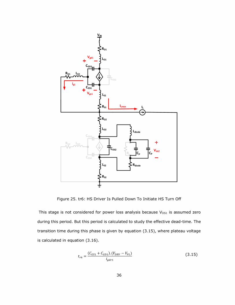
36
Rj
CGD1
CGS1
CDS1
LG1RG1
LD1
RD1
RS1
LS1
CGD2
CGS2
CDS2
LG2RG2
LD2
RD2
RS2
LS2
VIN
Ldiode
Rdiode
Cjr CP
ILILmax
ig1
Vgs1
Vgd1
Vds2
Figure 25. tr6: HS Driver Is Pulled Down To Initiate HS Turn Off
This stage is not considered for power loss analysis because VDS1 is assumed zero
during this period. But this period is calculated to study the effective dead-time. The
transition time during this phase is given by equation (3.15), where plateau voltage
is calculated in equation (3.16).
𝑡𝑟6 =(𝐶𝐺𝑆1 + 𝐶𝐺𝐷1). (𝑉𝐷𝑅𝑉 − 𝑉𝑃𝐿)
𝑖𝑔𝑑𝑟1
(3.15)

37
𝑉𝑃𝐿 = 𝑉𝑡ℎ +𝐼𝐿𝑚𝑎𝑥
𝑔𝑓𝑠
(3.16)
B. Stage 2(tr7: HS turn off period)
Rj
CGD1
CGS1
CDS1
LG1RG1
LD1
RD1
RS1
LS1
CGD2
CGS2
CDS2
LG2RG2
LD2
RD2
RS2
LS2
VIN
Ldiode
Rdiode
Cjr CP
ILILmax
ig1
Vgs1
Vgd1
Vds1
Figure 26. tr7: HS Turn Off Period

38
During this period, as VGS2 drops below VPL, the channel current of HS starts
to decrease. The equivalent circuit during this phase is shown in Figure 26. The rate
of change of drain current of HS and LF FET is limited by the parasitic inductances in
the loop. A faster gate loop will cause ich1 to drop to zero before the Schottky diode
is at maximum forward bias potential. The equivalent output capacitor of HS CDS1
starts charging and IDS1 drops from ILmax to zero. The presence of a higher reverse
capacitance from the Schottky diode decreases the rate at which the switch node
voltage drops. This period ends when VDS2 = 0. This period can be calculated from
[15], and is given by equation (3.17).
𝑡𝑟7 =(𝐶𝐺𝑆1 + 𝐶𝐺𝐷1). 𝐼𝐿𝑚𝑎𝑥 . 𝑅𝐺1(𝑜𝑓𝑓) − 𝐼𝐿𝑚𝑎𝑥 . 𝐿𝑆 . 𝑔𝑓𝑠
𝐼𝐿𝑚𝑎𝑥
2 −𝐶𝐺𝐷1. 𝐼𝐿𝑚𝑎𝑥 . 𝑅𝐺1(𝑜𝑓𝑓) . 𝑔𝑓𝑠
2. 𝐶𝐷𝑆1
(3.17)
C. Stage 3(tr8: turning on delay for Schottky diode)
This period signifies the time taken to completely turn on the Schottky diode. The
equivalent circuit during this phase is shown in Figure 27. The transition time is
derived and given in equation (3.18).
𝑡𝑟8 =2. 𝐶𝑃 . (𝑉𝑑)
𝐼𝐿𝑚𝑎𝑥
(3.18)

39
Rj
CGD1
CGS1
CDS1
LG1RG1
LD1
RD1
RS1
LS1
CGD2
CGS2
CDS2
LG2RG2
LD2
RD2
RS2
LS2
VIN
Ldiode
Rdiode
Cjf CP
IL
Vds1
ILmax
Vds2
Figure 27. tr8: Turning On Delay For Schottky Diode
D. Stage 4(td3: dead-time after HS turn off)
As discussed before, if the dead-time is not optimized for a regular buck converter
without an anti-parallel Schottky diode, the conduction losses in the dead-time will
be very high. The Schottky diode limits this to around -0.3V without having the need
to design a complex circuit to optimize dead-time. The conduction time is set by the
controller is tdead-time2. The equivalent circuit during this phase is shown in Figure 28.

40
This stage ends when the LS FET gate is pulled high. This transition period is given
by equation (3.19), which is a byproduct of tr6, tr7, tr8 and tdead-time2.
𝑡𝑑3 = 𝑡𝑑𝑒𝑎𝑑−𝑡𝑖𝑚𝑒2 − (𝑡𝑟6 + 𝑡𝑟7 + 𝑡𝑟8) (3.19)
Rj
CGD1
CGS1
CDS1
LG1RG1
LD1
RD1
RS1
LS1
CGD2
CGS2
CDS2
LG2RG2
LD2
RD2
RS2
LS2
VIN
Ldiode
Rdiode
Cjf CP
IL
ILmax
VD
Vds1
Figure 28. td3: Dead-Time Period After HS Turn Off
E. Stage 5(td4: dead-time after LS turn on)

41
Rj
CGD1
CGS1
CDS1
LG1RG1
LD1
RD1
RS1
LS1
CGD2
CGS2
CDS2
LG2RG2
LD2
RD2
RS2
LS2
VIN
Ldiode
Rdiode
Cjf CP
IL
VDRV
VD
ILmax
ig2
Vgs2
Vgd2
Vds1
Figure 29. td4: Dead-time After LS Turn On
The equivalent circuit for this phase is shown in Figure 29. At the beginning
of this transition, the LS gate driver is pulled high and the LS gate capacitor starts
charging. The conduction through the Schottky diode continues until VGS2 = Vgdth. The
time period for this stage is given in equation (3.20). This stage ends when VGD2
reaches Vgdth.

42
𝑡𝑑4 =(𝐶𝐺𝑆2 + 𝐶𝐺𝐷2). (𝑉𝑔𝑑𝑡ℎ − 𝑉𝑑)
𝐼𝑔𝑑𝑟1
(3.20)
F. Stage 6(tr9: turning off delay for the Schottky diode and LS turn on)
Rj
CGD1
CGS1
CDS1
LG1RG1
LD1
RD1
RS1
LS1
CGD2
CGS2
CDS2
LG2RG2
LD2
RD2
RS2
LS2
VIN
Ldiode
Rdiode
Cjr CP
IL
VDRV
Vds1
ILmax
Vds2
ig2
Vgs2
Vgd2
Figure 30. tr9: Turning Off Delay For Schottky Diode And LS Turn On
The equivalent circuit for this stage is given in Figure 30. This time can be
calculated the same as tr9 from Stage 3, given by equation (3.21).

43
𝑡𝑟9 =2. 𝐶𝑃. (𝑉𝑑)
𝐼𝐿𝑚𝑎𝑥
(3.21)
G. Stage 7(tr10: remaining rise period of LS)
Rj
CGD1
CGS1
CDS1
LG1RG1
LD1
RD1
RS1
LS1
CGD2
CGS2
CDS2
LG2RG2
LD2
RD2
RS2
LS2
VIN
Ldiode
Rdiode
Cjr CP
IL
VDRV
ILmax
ig2
Vgs2
Vgd2
Vds1
Figure 31. tr10: Remaining Rise Period Of LS

44
The input capacitor charges above Vgdth and the LS FET conducts dissipating
current in the channel. The equivalent circuit for this stage is given in Figure 31. This
transition period is not calculated here because this phase does not contribute to the
switching loss.

45
3.4 Process Flow Diagram
The transition times for every phase are calculated in section 3.2 and section 3.3
using piecewise analysis. These timing values are used to derive the switching power
losses during one clock cycle of the converter and the effective dead-time expression,
which will be detailed in chapter 4. The transition times calculated will be verified to
the simulated and the measured values from the transition waveforms in Chapter 4.
The process flow diagram for the modeling sequence is shown in Figure 32.
Figure 32. Process Flow Diagram For The Analytical Modeling

46
4. MODEL VERIFICATION AND DIODE CHARACTERIZATION
An industrial controller and driver have been used to design a buck converter
in Figure 33 using GaN FETs for switching frequencies, 400 KHz and 2 MHz. The
key parameter ranges for converter design are specified in Table 3.
VIN
VOUT
CO
LODead Time Control
(Non Overlapping Clock)
RO
CLK_PWM
Ton = D.T
T HS Driver
td
BOOTSTRAP
VSW
VDRV
VBSTR
VDRV
VBSTR
LS Driver
CLK_HS
CLK_LS
VSW
CLK_HS
CLK_LS
Figure 33. System Overview Of The Designed Buck Converter Power Stage
Parameter Design Range Unit
Input Voltages 8 - 20 V
Output Voltages 1.5 - 5 V
Switching Frequency 0.4 and 2 MHz
Load Current 0.5 - 6 A
Dead-time 10 - 110 ns
Table 3. Design Specifications

47
For calculation of effective dead-time from the analytical model, different
transition phases were analyzed. The dead-time period for LS off to HS on transition
(effective dead-time 1) that is set by the dead-time generating block can be
calculated from the difference in the moments when the LS driver is pulled low to
when the HS driver is pulled high. But, the effective dead-time is the one seen at the
switch node, which varies according to the inductor current. The dead-time period
for HS off to LS on transition (effective dead-time 2) follows the same principle.
Effective dead-times are derived in equations ((4.1) and ((4.2).
𝑒𝑓𝑓𝑒𝑐𝑡𝑖𝑣𝑒 𝑑𝑒𝑎𝑑𝑡𝑖𝑚𝑒 1 = 𝑡𝑟2 + 𝑡𝑑1 + 𝑡𝑑2 + 𝑡𝑟3 (4.1)
𝑒𝑓𝑓𝑒𝑐𝑡𝑖𝑣𝑒 𝑑𝑒𝑎𝑑𝑡𝑖𝑚𝑒 2 = 𝑡𝑟8 + 𝑡𝑑3 + 𝑡𝑑4 + 𝑡𝑟9 (4.2)
The total power loss can be estimated from the analytical models as a sum of
conduction loss, switching loss, reverse conduction loss, and gate drive loss, which
are given in expressions ((4.3) to ((4.6).
𝑆𝑤𝑖𝑡𝑐ℎ𝑖𝑛𝑔 𝐿𝑜𝑠𝑠 = 𝑓𝑠𝑤 . [ ∫ 𝑖𝐷𝑆2. 𝑣𝐷𝑆2.
𝑡𝑟2
0
𝑑𝑡 + ∫ 𝑖𝐷𝑆2. 𝑣𝐷𝑆2.
𝑡𝑟3
0
𝑑𝑡 + ∫ 𝑖𝐷𝑆1. 𝑣𝐷𝑆1.
𝑡𝑟3
0
𝑑𝑡
+ ∫ 𝑖𝐷𝑆1. 𝑣𝐷𝑆1.
𝑡𝑟4
0
𝑑𝑡 + ∫ 𝑖𝐷𝑆2. 𝑣𝐷𝑆2.
𝑡𝑟7
0
𝑑𝑡 + ∫ 𝑖𝐷𝑆2. 𝑣𝐷𝑆2.
𝑡𝑟8
0
𝑑𝑡
+ ∫ 𝑖𝐷𝑆1. 𝑣𝐷𝑆1.
𝑡𝑟7
0
𝑑𝑡 + ∫ 𝑖𝐷𝑆1. 𝑣𝐷𝑆1.
𝑡𝑟8
0
𝑑𝑡 + ∫ 𝑖𝐷𝑆2. 𝑣𝐷𝑆2.
𝑡𝑟9
0
𝑑𝑡]
(4.3)
𝐷𝑒𝑎𝑑𝑡𝑖𝑚𝑒 𝐿𝑜𝑠𝑠 = 𝑓𝑠𝑤 . [ ∫ 𝑖𝐷𝑆2. 𝑣𝐷𝑆2.
𝑡𝑑1+𝑡𝑑2
0
𝑑𝑡 + ∫ 𝑖𝐷𝑆1. 𝑣𝐷𝑆1.
𝑡𝑑3+𝑡𝑑4
0
𝑑𝑡] (4.4)
𝐺𝑎𝑡𝑒 𝐷𝑟𝑖𝑣𝑒 𝐿𝑜𝑠𝑠 = 2. 𝑓𝑠𝑤 . [𝐶𝐺𝑆1 + 𝐶𝐺𝐷1 + 𝐶𝐺𝑆2 + 𝐶𝐺𝐷2 ]. 𝑉𝐷𝑅𝑉2 (4.5)
𝐶𝑜𝑛𝑑𝑢𝑐𝑡𝑖𝑜𝑛 𝐿𝑜𝑠𝑠 = 2. 𝑓𝑠𝑤 . [ 𝑅𝐷𝑆(𝑜𝑛) + 𝑅𝐸𝑆𝐿]. 𝐼𝐿2 (4.6)
4.1 Measurement Setup
A single phase hard switching buck converter (shown in Figure 34) was measured
for different cases to verify switching operation under different dead-time values. A

48
TI driver, LM5113, was used to drive low voltage enhancement mode GaN part
number: 2014C from EPC. Dead-time was adjusted within a range of 10ns to 90ns.
An external waveform generator was used to set the switching frequency in the range
from 400 KHz to 2 MHz. The measurement setup is shown in Figure 35.
VIN
VOUT
CO
LO
RO
HS Driver
VSW
VDRV
VBSTR
LS Driver
CLK_LS
EPC8010
2 µF
100 nF 200 nF27 k VDRV
+
-
CLK_PWM
CLK_HS
CLK_LS
Figure 34. Buck Converter Design

49
Figure 35. Hardware Measurement Set-Up
4.2 Model Verification
The total loss can be derived from conduction loss and switching loss. The main
sources of conduction loss are channel resistances from the HS and LS FETs and the
effective series resistance loss of the output inductor. The main sources of switching
loss are the loop resistances set by the PCB tracks, voltage controlled current sources
of the HS and LS FETs, and the conduction loss from the Schottky diode. High
frequency turn-on and turn-off ringing loss is also added to the analysis.
For a broader understanding of the buck converter with GaN power FETs, a buck
converter with synchronous rectifier was designed and simulated using EPC2014C for

50
the high side and low side FETs. The simulation model was provided by EPC in LTSpice
software.
Figure 36. LS Off And HS On Transition Simulation
Figure 37. HS Off And LS On Transition Simulation

51
Figure 36 shows simulations for time period calculation for each phase in switching
transitions from LS turn-off to HS turn-on and
Figure 37 shows simulations for time period calculation for each phase switching
transitions from HS turn-off to LS turn-on at 2MHz and 1A load current. The values
obtained from model are compared to simulated and measured results.
Figure 38. Transition Time Correlation at 400 KHz For 12V To 3.3V Conversion
Figure 39. Transition Time Correlation at 2 MHz For 12V To 3.3V Conversion

52
Figure 38 and Figure 39 show correlation of the calculated values of transition
time phases to simulated and measured results. To observe the contribution of
reverse conduction loss to total power loss of the buck converter, simulations were
done at varying dead-time and load currents for two cases: with and without a
Schottky diode in parallel with the synchronous LS FET. The switching frequencies at
which all calculations were done range from 400 KHz and 2 MHz with an input voltage
range of 8-20V to an output voltage range of 1.5-5V. A time domain snapshot of the
switch node voltage and diode current is shown in Figure 40 to show relation of diode
current with switch node voltage.
Figure 40. Switch Node Voltage And Diode Current At 400khz

53
Figure 41. Load Current Vs Efficiency At Optimized Dead-Times
Figure 41 shows an added advantage of the Schottky diode on the efficiency
of the converter for 400 KHz and 2 MHz at varying load currents from 500mA to 3A.
The converter’s efficiency improves by 2 to 3% when including an anti-parallel diode.
Figure 42 shows error between calculated and measured effective dead-times for 12V
to 3.3V at 1A load current. Figure 43 shows percentage error between calculated and
measured effective dead-times for 400 KHz switching frequency at different dead-
time values. A 25% error at lower dead-time values is observed due to the non-
optimized dead-time values set by the controller for a converter operating at 400
KHz. As per the measurements, around 90ns of optimum dead-time was observed
for this condition where the error is around 7%. Finally, Figure 44 shows the trend
for less variation in dead-times at higher load currents.

54
Figure 42. Effective Dead-Time Calculated And Measured
Figure 43. Percentage Error Between Calculated And Measured Effective Dead-
Times

55
Figure 44. Effective Dead-Time With Increasing Load Current
4.3 Diode Characterization
Different industry diodes are characterized based on the packaging and electrical
characteristics to categorize them by application and performance. For selection of a
Schottky diode, a selection criteria can be set by introducing a new parameter, Dlimit
that can be calculated from datasheet parameters, which is defined in equation
((4.7).
𝐷𝑙𝑖𝑚𝑖𝑡 =𝐼𝐹(𝑎𝑣𝑔)
𝐼𝐹(𝑟𝑚𝑠)
(4.7)
IF(avg) is the rated average forward current of the Schottky diode and IF(rms) is
the repetitive forward current (peak forward current) of the Schottky diode.
If 𝑡𝑑𝑒𝑎𝑑𝑡𝑖𝑚𝑒(𝑒𝑓𝑓𝑒𝑐𝑡𝑖𝑣𝑒) ×𝑓𝑠𝑤
𝐼𝐿𝑚𝑎𝑥< 𝐷𝑙𝑖𝑚𝑖𝑡, then the choice of the Schottky diode is limited by IF(rms).

56
If 𝑡𝑑𝑒𝑎𝑑𝑡𝑖𝑚𝑒(𝑒𝑓𝑓𝑒𝑐𝑡𝑖𝑣𝑒) ×𝑓𝑠𝑤
𝐼𝐿𝑚𝑎𝑥 ≥ 𝐷𝑙𝑖𝑚𝑖𝑡, then the choice of the Schottky diode is limited by
IF(avg).
4.4 Conclusions from Measurements
The effective dead-time observed from the switching analysis through
calculations, simulations, and measurements is different than the values set by the
controller, which happens due to the interaction between parasitic elements of the
power converter. Additional losses due to parasitic components of the Schottky diode
add to total power loss. The diode must be rated for the maximum inductor current
with lowest parasitic inductances otherwise high amplitude ringing is observed during
both the dead-times which increases power loss by 1-2%. Analytical model transition
time values are correlated to simulations and measured results, and the developed
model shows good correlation with simulations and measured results at 400 KHz and
2 MHz with 1A load current. It has been concluded that the developed model
effectively predicts power stage performance for a low side FET using anti-parallel
diode in GaN-based PoL buck converters.

57
5. MODEL COMPARISON TABLE AND CONCLUSION
5.1 Analytical Model Summary
Parameter TPE 2016 JESTPE 2019 TIE 2020 This work
Synchronous FET analysis
Not present Present Present Present
Dead-time Analysis
Not present Not present Present* Present (analysis)
Switching frequency
2MHz 400KHz, 700KHz and 1MHz
2MHz 400KHz, 1MHz, 4MHz
Converter
ratio
12V - 3.6V 12V – 1.2V 12V – 3.3V 20V - 5V, 12V
-3.3V,and 8V – 1.5V
Max. Output Power
26W 18W 26W 30W
Max. Load Current
7.9A 15A 8A 6A
GaN device EPC 2015 EPC 2015C EPC 2015 EPC 2014C
Driver LM5113 LM5113 LM5113 LM5113
Max. Efficiency
89.5% 93% 89.9% 93%
Model Novelty
First analytical switching model for eGaN main FET only
Comparison of analysis with and without Synchronous FET
Addition of parasitic elements for high switching frequency
Analysis with anti-parallel Schottky diode with SR FET
Analysis technique
Average power calculation using circuit parameter
values obtained from FEA method
On/Off Transition time
analysis
Average power calculation using circuit parameters
from FEA method (excludes dead-time loss)
On/Off transition time and dead-time loss analysis

58
Parameter TPE 2016 JESTPE 2019 TIE 2020 This work
Additional Information
Novel current measuring method based on magnetic coupling
Categorization of Schottky diodes to improve performance of converter
Table 4. Comparison With Prior Work
5.2 Future Work/Improvements
This model can be further developed for extremely low load currents that
modify the operation of the buck converter. The proposed model can be updated and
expanded to analyze the power loss in other power converter topologies. This model
can also be used to analyze losses before the development of adaptive dead-time
control strategies.
With an integrated GaN and Schottky as a system-in-chip, the switching
performance of a buck converter using GaN can be significantly improved for PoL
applications. Control architectures for optimized dead-time using adaptive dead-time
techniques can be implemented to improve converter efficiency.

59
REFERENCES
[1] M. David Kanakam and Malik E. Elbuluk, "A Survey of Power Electronics Applications in Aerospace Technologies," in 36th Intersociety Energy Conversion Engineering Conference, Georgia, Aug 2001.
[2] B. Baliga, Fundamentals of Power Semiconductor Devices, New York, NY, United States: Springer, 2008.
[3] "https://www.bloomberg.com/press-releases/2019-08-26/," [Online]
[4] D. Maksimovic and R. W. Erickson, Fundamntals of Power Electronics, Second Edition, Springer, 2001.
[5] O. Kirshenboim and M. M. Peretz, "High Efficiency Nonisolated Converter With Very High Step-Down Conversion Ratio," IEEE Trans. on Power Electron., vol. 32, no. 5, pp. 3683 - 3690, May 2017.
[6] A. Hegde, Y. Long and J. Kitchen, "A comparison of GaN-based power stages for high-switching speed medium-power converters," 2017 IEEE 5th Workshop on Wide Bandgap Power Devices and Applications (WiPDA), Albuquerque, NM, 2017, pp. 213-219.
[7] B. K. Rhea et al., "A 12 to 1 V five phase interleaving GaN POL converter for high current low voltage applications," 2014 IEEE Workshop on Wide Bandgap Power Devices and Applications, Knoxville, TN, 2014, pp. 155-158.
[8] TexasInstruments, "LMG3411R150 datasheet," March 2019. [Online]. Available: https://www.ti.com/product/LMG3411R150
[9] X. Ren, D. Reusch, S. Ji, Z. Zhang, M. Mu and F. C. Lee, "Three-level driving method for GaN power transistor in synchronous buck converter," 2012 IEEE Energy Conversion Congress and Exposition (ECCE), Raleigh, NC, 2012, pp. 2949-2953.
[10] Y. Zhang, C. Chen, T. Liu, K. Xu, Y. Kang and H. Peng, "A High Efficiency Model-Based Adaptive Dead-Time Control Method for GaN HEMTs Considering Nonlinear Junction Capacitors in Triangular Current Mode Operation," in IEEE Journal of Emerging and Selected Topics in Power Electronics, vol. 8, no. 1, pp. 124-140, March 2020.
[11] D. Reusch, D. Gilham, Y. Su and F. C. Lee, "Gallium Nitride based 3D integrated non-isolated point of load module," 2012 Twenty-Seventh Annual IEEE Applied Power Electronics Conference and Exposition (APEC), Orlando, FL, 2012, pp. 38-45.
[12] “EPC2014C datasheet”, EPC. [Online]

60
[13] W.Eberle, Z.Zhang, Y.Liu and P.C.Sen, "A Practical Switching Loss Model for Buck Voltage Regulators," IEEE Trans. Power Electron., vol. 24, no. 3, pp. 700-713, Mar. 2009.
[14] K. Wang, X. Yang, H. Li, H. Ma, X. Zeng and W. Chen, "An Analytical Switching Process Model of Low-Voltage eGaN HEMTs for Loss Calculation," in IEEE Transactions on Power Electronics, vol. 31, no. 1, pp. 635-647, Jan. 2016.
[15] Y. Xin et al., "Analytical Switching Loss Model for GaN-Based Control Switch and Synchronous Rectifier in Low-Voltage Buck Converters," in IEEE Journal of Emerging and Selected Topics in Power Electronics, vol. 7, no. 3, pp. 1485-1495, Sept. 2019.
[16] J. Chen, Q. Luo, J. Huang, Q. He and X. Du, "A Complete Switching Analytical Model of Low-Voltage eGaN HEMTs and Its Application in Loss Analysis," in IEEE Transactions on Industrial Electronics, vol. 67, no. 2, pp. 1615-1625, Feb. 2020.
[17] D. Reusch,” Optimizing PCB Layout”, EPC. [Online]
[18] A. Y. Tang, V. Drakinskiy, K. Yhland, J. Stenarson, T. Bryllert and J. Stake,
"Analytical Extraction of a Schottky Diode Model From Broadband S-Parameters," in IEEE Transactions on Microwave Theory and Techniques, vol. 61, no. 5, pp. 1870-1878, May 2013.
[19] "SBR130S3 datasheet," Diodes Incorporated, April 2015. [Online]. Available: https://www.mouser.com/datasheet/2/115/SBR130S3-464820.pdf