analysis, design and development of patch...
TRANSCRIPT

I J C T A, 9(9), 2016, pp. 3697-3703© International Science Press
Analysis, Design and Development ofPatch Antenna for S-Band ApplicationsB.G. Gopal1, P.G. Kuppusamy2, R. Kalpana3 and G. Vishnu Vardhan Rao4
ABSTRACT
Patch Antenna is a low profile antenna very much suitable for low frequency microwave application. This paperdeals the Analysis, Design and Development of Patch Antenna for Wireless medical applications in the range of2–4 GHz. The design parameters together with their relevant equations allow analytical calculations beforesimulation is performed. Finally a practical design is worked out to highlight the design steps required and CADsimulations are also described. The antenna is designed and analyzed using CST Microwave Studio. Here PTFE(Poly Tetra Fluoro Ethylene) material is used as substrate material, above which the rectangular patch is placed.The ground plane is incorporated with defective ground structure (DGS) to improve antenna performance. Thisantenna can be utilized for 4G frequency spectrum bandsand also for Industrial, Scientific and Medical (ISM)band applications. The antenna is fed with coaxial feed as waveguide port. The results presented that the antennahas gain of 7.4 dB. The simulation result provides that antenna can provide better gain and directivity. DGSwhich is realized by is a form of periodic structure has ability to reject certain frequency bands and passescertain frequency bands with less attenuation. Thus it improves gain and directivity. The Return loss, VSWR,radiation pattern and gain are observed.
Keywords: Patch Antenna, Return loss, VSWR, Radiation Pattern, Gain
1. INTRODUCTION
The evolution of wireless technologies is flavored into different generations depending on the maturitylevel of underlying technology. The patch antenna was proposed in 1953 by Deschamps. The classificationsinto these generations are not based on any parameters. Efforts have been made for the development of 4G(LTE) wireless technology [2]. The 3G (ITU) is limited to maximum bit rate factor of 10 and user planetraffic (UMTS>30msec). The resource assignment procedure is too big to handle traffic with high bit rate.It provides better spectrum efficiency, high data rates and lower latencies, flatter IP core architecture whenit is compared with 3G technology [1]. The patch antenna presented here is a type of microstrip antenna. Itconsists of dielectric substrate sandwiched between the ground plane and the patch. It is virtually a parallelplate capacitor. When the patch size is proportional to signal frequency, it resonates at some frequencies.The application of Microstrip patch antenna due to its low profile, compactness, low cost, manufacturingrepeatability extends widely. The practical drawbacks of micro strip antenna are it offers narrow bandwidthand low gain because of conductor, dielectric and surface wave losses. The losses depend on substratethickness, permittivity and tanä of the material. To improve gain further, patch antenna is designed withDGS on ground plane which provides compactness and high gain. The DGS is a technique used to etchdefected pattern on the back side of the ground plane [3].
1 Associate Professor, Department of Electronics and Communication Engineering, Vel TechMultitech, Chennai, India,Email: [email protected]
2 Professor, Department of Electronics and Communication Engineering, Vel TechMultitech, Chennai, India,Email: [email protected]
3, 4 Assistant Professor, Department of Electronics and Communication Engineering, Vel TechMultitech, Chennai, India,Email: [email protected]

3698 B.G. Gopal, P.G. Kuppusamy, R. Kalpana and G. Vishnu Vardhan Rao
2. ANTENNA DESIGN PROCEDURE
The following sections deal the design of patch antenna. Patch antennas performance depends on certainparameters which are calculated and utilized in this project. The operating frequency (f
0 = 3GHz), substrate
permittivity (�r= 2), substrate height (h = 1.9 mm) and loss tangent (tan � = 0.0013) are first selected for the
targeted gain. From the known parameters, the unknown parameters such as length Lpand width W
p of the
patch, length Lg and width W
g of the ground are calculated using the empirical formulae below.
The width of the patch is
0
2
2 1pr
cW
f (1)
The effective permittivity (�eff)
of the substrate is
121 1 12
12 2
r reff
p
h
w(2)
Effective length is
22
eff p
o eff
cL L L
f (3)
where �L is fringing field length extension written as
0.3 0.264
0.412
0.258 0.8
peff
peff
w
hL h
w
h
(4)
The length of patch is given by
0
22
p
eff
cL L
f (5)
The length (Ls) and width (W
s) of the substrate are
6
6
s p g
s p g
L L h L
W W h W (6)
which are also the dimensions of the ground plane
3. ANTENNA CONFIGURATION
The constraints of the antenna design are the size of the device, substratematerial and location of the feedpoint. The antenna structure is printed on PTFE (Poly Tetra Fluoro Ethylene) substrate. The geometry ofthe antenna is shown in Figure 1 and Figure 3. The physical dimensions are given in the Table 1. Theground plane should be greater than the patch dimension. The ground plane has 18mm×16mm×5mm andthe patch has 12mm × 10mm × 3mm. The substrate material is Poly Tetra Fluoro Ethylene (PTFE) withpermittivity of 2 with thickness 1.9mm. The patch shape plays a crucial role in approaching compactness

Analysis, Design and Development of Patch Antenna for S-Band Applications 3699
and improved gain. A 50� coaxial probe feed is used to feed the patch since it a low cost feeding techniqueand can be easily affixed. The feed point position is located in such a way to provide good impedancematching.
3.1. Coaxial probe Feeding Method
The patch antenna can be excited by different methods like in fed line method, microstrip line feed andcoaxial probe feed methods. In our case, it is fed with coaxial probe which has characteristic impedance of50 ohm. The inner conductor of the probe is attached to the patch at a particular feed position from the backof the ground plane without touching the ground plane. The outer conductor is connected to the groundplane. Hence the coupling offers pure inductive reactance in nature. The coaxial cable has central conductorradius of 0.63 mm, outer conductor radius as 2.5 mm and the radius of the inner dielectric is 2.25 mm madeof Teflon of �
r = 2.1
The equivalent circuit of coaxial feed patch is shown in Figure 2, which denotes the inductive part dueto inner conductor.
We are using PTFE as the dielectric material of dielectric constant 2. The position of the probe plays animportant role in effectively radiating the energy into space. The probe must be connected at a point wherethe impedance is nearly equal to 50 ohm. This can be calculated theoretically since we know the impedanceat the corner of the patch. The values of the impedance for the coaxial probe feed follows direct proportionality
Table 1Design Parameters of the Rectangular Patch Antenna
Parameter Dimension
Lp
34.37 mm
Wp
33.33 mm
Ls
45.77 mm
Ws
44.7 mm
Substrate height h 1.9 mm
Er
2
Figure 1: Geometry of Patch Antenna

3700 B.G. Gopal, P.G. Kuppusamy, R. Kalpana and G. Vishnu Vardhan Rao
with 2 0yCos
L where y
0 is the distance of the point of impedance observation from the patch edge. The
impedance at y = y0 from patch edge is
0
2 00yy y
yZ Z Cos
L (7)
The impedance of the coaxial line is
60ln
r
bZ
a (8)
where ‘b’ is the radius of the outer conductor and ‘a’ is the radius of the inner conductor. But practicalpurpose the empherical formula to determine the feed point location is
pf
eff
LX and
2p
f
wY (9)
4. SIMULATION AND RESULTS
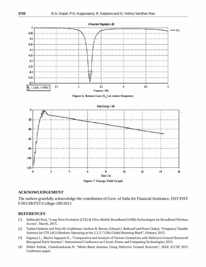
With the above parameter values, the patch antenna is designed and simulated. The following figuresclearly depict the results offered by the antenna. The gain, radiation pattern, returns loss and energy fieldpattern are shown in the following Figure 4 to Figure 7.
5. CONCLUSION
Design, Analysis and Performance improvement of Patch Antenna are presented for applications in thefrequency range of 2 – 4 GHz. The Gain and radiation pattern of the antenna can be improved with addedperiodic structures in the ground plane. The proposed ground structure in the patch antenna could achievehigher gain than the normal patch antenna. The S parameter and total efficiency were measured to validatethe simulation results.
Figure 2: Equivalent circuit of Patch Antenna

Analysis, Design and Development of Patch Antenna for S-Band Applications 3701
Figure 3: Top view of the half patch antenna with bottom coaxial feed
Figure 4: Gain of Antenna
Figure 5: Radiation Pattern and Directivity of Antenna
3702 B.G. Gopal, P.G. Kuppusamy, R. Kalpana and G. Vishnu Vardhan Rao
Figure 7: Energy Field Graph
Figure 6: Return Loss (S11
) at center frequency
ACKNOWLEDGEMENT
The authors gratefully acknowledge the contribution of Govt. of India for Financial Assistance, DST-FISTF.NO:SR/FST/College-189/2013
REFERENCES[1] Subharthi Paul, “Long Term Evolution (LTE) & Ultra-Mobile Broadband (UMB) Technologies for Broadband Wireless
Access”, March, 2015.
[2] Tayfun Ozdemir and Yuriy M. Goykhman, Andrew R. Brown, Edward J. Rothwell and Prem Chahal, “Frequency TunableAntenna for LTE (4G) Handsets Operating in the 2.3-2.7 GHz Global Roaming Band”, Febuary, 2015.
[3] Suganya L., Martin Sagayam K., “Comparative and Analysis of Various Geometries with Defective Ground StructuredHexagonal Patch Antenna”, International Conference on Circuit, Power and Computing Technologies, 2015.
[4] Nikhil Pathak, Chandrasekaran.N, “Multi–Band Antenna Using Defective Ground Structure”, IEEE ICCSP 2015Conference paper.

Analysis, Design and Development of Patch Antenna for S-Band Applications 3703
[5] Amit Singh Bhadouria, Mithilesh Kumar, “Microstrip Patch Antenna for Radiolocation using DGS with Improved Gainand Bandwidth”, IEEE International Conference on Advances in Engineering & Technology Research, August, 2014.
[6] Janne Ilvonen, RistoValkonen, Jari Holopainen and Vile Viikari, “Design Strategy for 4G Handset Antennas and a MultibandHybrid Antenna”, IEEE Transaction on Antenna and Propogation, Vol. 62, No. 4, April 2014.
[7] Sanjeeva R. Rama and D.Vakula, “Compact Multiband Patch Antenna with Fractal Defective Ground Structure for WirelessApplications”, IEEE International Microwave and RF Conference, 2014.