analog front end (afe) for sensing temperature in smart ... · 138 kv or 230 kv transmission lines...
TRANSCRIPT

24 bit û� ADCADS1248
SPI, I2CInterface
Connector
SPI
2 LEDs: RTD channel
beingsampled
AIN0
AIN1
AIN2
AIN3
AIN4
AIN5
AIN6
AIN7
Analog SwitchTS3A5017D
I2C I/O Expander
TCA6408AVrtd_Ch1
IEXC1_Ch1
IEXC2_Ch1
Ch2
Ch3
Ch4
IEXC1_Ch2
IEXC2_Ch2
IEXC1_Ch3
IEXC2_Ch3
IEXC1_Ch4
IEXC2_Ch4
Vrtd_Ch2
Vrtd_Ch3
Vrtd_Ch4
Control Lines
Power SupplyConnector
VDC
GND
I2C
LDO TPS7A1633DGNR
VDC +3.3V
Ch1
Vrtd_Ch4
Vrtd_Ch1
Vrtd_Ch2
Vrtd_Ch3
Control Lines
IEXC1
IEXC2
RTD
TI DesignsAnalog Front End (AFE) for Sensing Temperature in SmartGrid Applications Using RTD
TI Designs Design FeaturesTI Designs provide the foundation that you need • Based on the ADS1248 24-Bit Delta-Sigma (ΔΣ)including methodology, testing and design files to ADC With Internal PGA and Selectable Gainquickly evaluate and customize the system. TI Designs up to 128help you accelerate your time to market. • Can Measure 2-, 3-, or 4-Wire RTD Inputs
• Meets Requirements for Smart Grid ApplicationsDesign Resources• Uses Ratiometric Measurement for Higher
Design PageTIDA-00110 AccuracyADS1248 Product Folder • Matched Current DACs for RTD ExcitationTPS7A1633 Product Folder • Multiplexer (Analog Switch) to Switch ExcitationTCA6408A Product Folder Currents for Four RTD InputsTS3A5017D Product Folder • Accuracy < ±2°C Without Calibration for Pt100CSD17571Q2 Product Folder
• I2C I/O Expander for ADC Interface Control andADS1148 Product FolderExcitation Current Switching Provided (No ExternalI/Os Required)
ASK Our E2E Experts Featured ApplicationsWEBENCH® Calculator Tools
• Protection Relays• RTD Extension Modules for Protection Relay• Remote Terminal Units
An IMPORTANT NOTICE at the end of this TI reference design addresses authorized use, intellectual property matters and otherimportant disclaimers and information.
All trademarks are the property of their respective owners.
1TIDU575–December 2014 Analog Front End (AFE) for Sensing Temperature in Smart Grid ApplicationsUsing RTDSubmit Documentation Feedback
Copyright © 2014, Texas Instruments Incorporated

System Description www.ti.com
1 System Description
1.1 Resistance Temperature DetectorTemperature is one of the oldest known physical quantities. Temperature is the most essential factor thatneeds continuous measurement and monitoring in smart grid. Today, the industry demands accurate,repeatable, and reliable measurement of temperature, because temperature can have a significant impacton product cost, quality, efficiency, and safety.
Temperature sensors types include:• Resistance temperature detector (RTD)• Thermistor• Thermocouple
Figure 1. Comparison of Different Temperature Sensors Used for Smart Grid Applications
The focus of this design is to measure temperature using RTD, a sensing element whose resistancechanges with the temperature. The relationship between the resistance and temperature of an RTD ishighly predictable, which allows accurate and repeatable temperature measurement over a wide range.
2 Analog Front End (AFE) for Sensing Temperature in Smart Grid Applications TIDU575–December 2014Using RTD Submit Documentation Feedback
Copyright © 2014, Texas Instruments Incorporated

PGAΔΣ
ADC
RREF
RRTD
REFP REFN
I1
VIN-
VIN+
VDIFF
VR
I=
www.ti.com System Description
1.1.1 RTD MeasurementThe basic principle of RTD measurement is based on the Ohm’s law equation:
where• R = Resistance of the RTD element• I = Known excitation current• V = Voltage across RTD element (1)
RTDs require constant current source for its excitation to produce a voltage output proportional to theresistance of the RTD. The resulting voltage output is measured by the analog-to-digital converter (ADC).The RTD voltage is amplified based on the requirement. Based on the measured voltage, the RTDresistance or temperature is calculated. Depending on the RTD type, different excitation currents can beused. The RTDs are available in different lead wire configurations: 2-, 3-, and 4-wire.
1.1.2 Ratiometric MeasurementA ratiometric approach guarantees more effective number of bits (ENOBs) as the noise in the IDACreflects in the reference and as well as in the input and hence tends to cancel off. The effect of the IDACcurrent temperature drift also gets canceled off in this ratiometric topology.
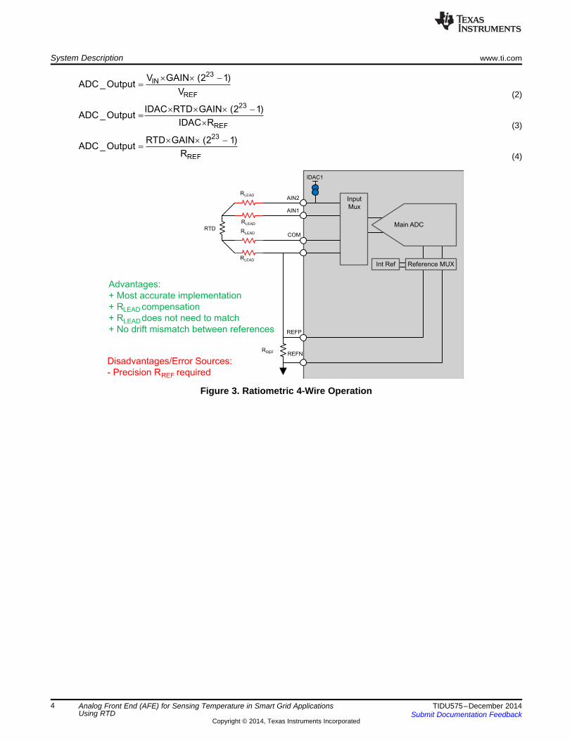
ADC requires a reference voltage to convert the input voltage into a digital output. In most applications,this reference is fixed and generated either internal or external to the ADC. The voltage reference hasdirect influence on the accuracy of output. If the measurement can be configured such that the ADC resultis a ratio of the input and a precision element such as a resistor, then much higher precision results canbe obtained. In ratiometric configuration, the excitation current that flows through the RTD returns toground through a low-side reference resistor, RREF. The voltage developed across RREF is fed into thepositive and negative reference pins (REFP and REFN) of the ADC and ADS1248 is configured to use thisexternal reference voltage VREF for the analog-to-digital conversions. Select RREF as a low-tolerance, low-drift resistor for accurate results.
The voltage drop across the RTD and RREF resistors is produced by the same excitation source and theADC output code is a relationship between the input voltage and the reference voltage. Therefore, errorsas a result of the absolute accuracy of the excitation current and the errors because of excitation drift arevirtually eliminated. In addition, the noise of the excitation source at the inputs is also reflected on thereference path of the ADC and, in this manner, cancels the noise. Therefore, the system becomesimmune to variations in the excitation.
Figure 2. Simplified Circuit for RTD Ratiometric Measurement
3TIDU575–December 2014 Analog Front End (AFE) for Sensing Temperature in Smart Grid ApplicationsUsing RTDSubmit Documentation Feedback
Copyright © 2014, Texas Instruments Incorporated
Reference MUXInt Ref
Main ADC
Input
Mux
RLEAD
RLEAD
RLEAD
RLEAD
RTD
AIN2
AIN1
COM
REFP
REFN
IDAC1
RREF
Advantages:
+ Most accurate implementation
+ R compensation
+ R does not need to match
+ No drift mismatch between references
Disadvantages/Error Sources:
- Precision R required
LEAD
LEAD
REF
23
REF
RTD GAIN (2 1)ADC _ Output
R
´ ´ -
=
23
REF
IDAC RTD GAIN (2 1)ADC _ Output
IDAC R
´ ´ ´ -
=
´
23IN
REF
V GAIN (2 1)ADC _ Output
V
´ ´ -
=
System Description www.ti.com
(2)
(3)
(4)
Figure 3. Ratiometric 4-Wire Operation
4 Analog Front End (AFE) for Sensing Temperature in Smart Grid Applications TIDU575–December 2014Using RTD Submit Documentation Feedback
Copyright © 2014, Texas Instruments Incorporated

Two-wire RTD Three-wire RTD Four-wire RTD
RTD RTD RTD
www.ti.com System Description
1.1.3 Connecting 2-, 3-, and 4-Wire RTD InputsThis module is compatible with 2-, 3-, and 4-wire RTD inputs. The connection diagrams for connectingthem to the module are shown in Figure 4. The user just needs to connect jumper wires externally asindicated by the red-colored wires. This arrangement does not call for any change in the hardware on themodule and is quite useful when user can access only the interface connectors.
Figure 4. Different RTD Input Connections
Table 1. RTDs Used in Smart Grid
RTD TYPE TEMPERATURE COEFFICIENT OF RESISTANCE (TCR) / °C100-Ω platinum 0.00385250-Ω platinum 0.00385
100-Ω nickel 0.00618120-Ω nickel 0.0061810-Ω copper 0.00427
Table 2 shows the resistance versus temperature for different types of RTDs.
Table 2. RTD Resistance versus Temperature
RTD TYPETEMPERATURE (°C)
Pt100 Ni100 Ni120 Cu10300 212.02 — 439.44 —200 175.84 223.20 303.46 16.78100 138.50 161.80 200.64 12.9090 134.70 154.90 191.64 12.5180 130.89 148.30 182.84 12.1270 127.07 141.70 174.25 11.7460 123.24 135.30 165.90 11.3550 119.40 129.10 157.74 10.9740 115.54 123.00 149.79 10.5830 11.67 117.10 142.06 10.1920 107.79 11.20 134.52 9.8110 103.90 105.60 127.17 9.420 100.00 100.00 120.00 9.04
–10 96.09 94.60 113.00 8.65–20 92.16 89.30 106.15 8.26–30 88.22 84.10 99.41 7.88–40 84.27 79.10 92.76 7.49–50 80.31 — 86.17 7.10
5TIDU575–December 2014 Analog Front End (AFE) for Sensing Temperature in Smart Grid ApplicationsUsing RTDSubmit Documentation Feedback
Copyright © 2014, Texas Instruments Incorporated
Generation
Generating StationGenerator Step Up
TransformerTransmission Customer
138 kV or 230 kV
Transmission Lines500, 345, 230, and 138 kV
Substation Step-Down Transformer
Subtransmission Customer26 kV and 69 kV
Primary Customer 13 kV and 4 kV
Subtransmission Customer 120 V and 240 V
Transmission Distribution
System Description www.ti.com
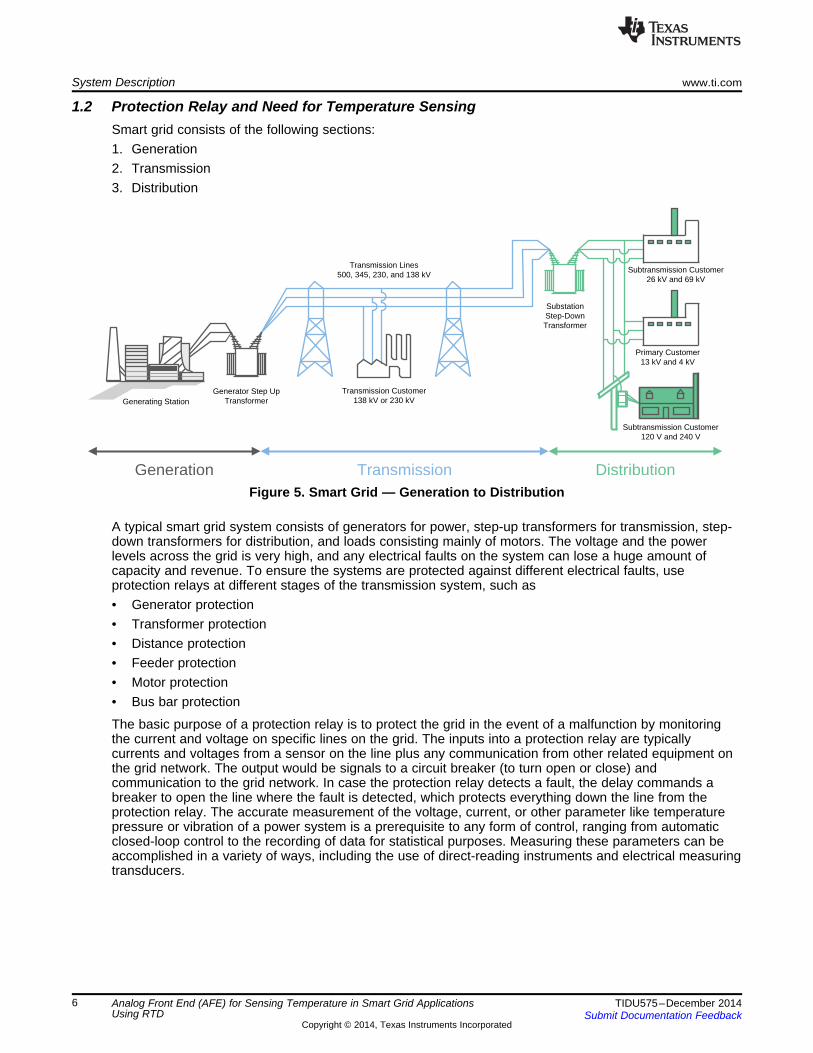
1.2 Protection Relay and Need for Temperature SensingSmart grid consists of the following sections:1. Generation2. Transmission3. Distribution
Figure 5. Smart Grid — Generation to Distribution
A typical smart grid system consists of generators for power, step-up transformers for transmission, step-down transformers for distribution, and loads consisting mainly of motors. The voltage and the powerlevels across the grid is very high, and any electrical faults on the system can lose a huge amount ofcapacity and revenue. To ensure the systems are protected against different electrical faults, useprotection relays at different stages of the transmission system, such as• Generator protection• Transformer protection• Distance protection• Feeder protection• Motor protection• Bus bar protection
The basic purpose of a protection relay is to protect the grid in the event of a malfunction by monitoringthe current and voltage on specific lines on the grid. The inputs into a protection relay are typicallycurrents and voltages from a sensor on the line plus any communication from other related equipment onthe grid network. The output would be signals to a circuit breaker (to turn open or close) andcommunication to the grid network. In case the protection relay detects a fault, the delay commands abreaker to open the line where the fault is detected, which protects everything down the line from theprotection relay. The accurate measurement of the voltage, current, or other parameter like temperaturepressure or vibration of a power system is a prerequisite to any form of control, ranging from automaticclosed-loop control to the recording of data for statistical purposes. Measuring these parameters can beaccomplished in a variety of ways, including the use of direct-reading instruments and electrical measuringtransducers.
6 Analog Front End (AFE) for Sensing Temperature in Smart Grid Applications TIDU575–December 2014Using RTD Submit Documentation Feedback
Copyright © 2014, Texas Instruments Incorporated
www.ti.com System Description
Protections relays measure the following parameters and based on the set threshold they protect:1. Currents2. Voltages3. Temperature4. Power direction
Most protection relays monitor temperature of the systems they protect.
Generator or Motor ProtectionGenerators are designed to run at a high load factor for a large number of years and permit certainincidences of abnormal working conditions. The machine and its auxiliaries are supervised by monitoringdevices to keep the incidences of abnormal working conditions down to a minimum. Despite themonitoring, electrical and mechanical faults can occur, and the generators must be provided withprotective relays, which, in case of a fault, quickly disconnect the machine from the system and, ifnecessary, completely shut down the machine. Thermal overload protection is one such protection. Formotor protection, the relay monitors temperature of the following: motor winding, motor bearing, loadbearing, and auxiliary winding.
Transformer ProtectionTransformers are a critical and expensive component of the power system. Due to the long lead time forrepair of and replacement of transformers, a major goal of transformer protection is to limit the damage toa faulted transformer. Temperature-based protection can aid this goal by identifying operating conditionsthat may cause transformer failure. Transformer protection relay monitors temperature of primary orsecondary winding hot-spots, the oil at the bottom and top of the transformer, and the ambient air. AnRTD input can also be used as a direct resistance measuring input for position tracking of an on-load tapchanger.
The number of sensors depends on the size of the motor, generator, and transformer. Protection relaysprovide a certain number of RTDs. Many applications may need to monitor more RTDs and multiplemotors, generators, or transformers using one protection relay. An RTD expansion module is used alongwith the protection relay to sense the temperature inputs, compute the temperatures and communicate thetemperature values to the relay for protection. Different types of RTD can be used based on theapplications. The accuracy of measurement for different sensors is expected to be the same and high. Anaccurate ADC is required to measure the temperature. An ADC with internal PGA ensures multiple typesof RTD connection. A current source is required to excite the RTDs for measured. If the current source isintegrated with the ADC, the complexity of design reduces and ensured better accuracy.
Some of the protections required in each segment are:• For power generation: Generator protection, breaker protection, and transformer protections• For transmission: Transformer protection, line voltage differential protection, and line distance
protections• For distribution: Transformer protection, motor protection, air circuit breakers, and molded case circuit
breakers
Since a number of RTDs are connected to one expansion module or protection relay the conversion timeof the ADC is important. The temperature is a slow varying signal, so the number of samples to bemeasured per second will be less. It is preferred that all the RTD inputs are samples at least once asecond in a module that has 12 RTDs. Higher resolution ADCs with PGA, matched current source andradiometric measurement techniques, are used to improve accuracy.
TI has a large portfolio of ΔΣ ADCs that suits the requirements for RTD measurements. Additional to theresolution, TI ΔΣ ADCs have a high level of integration including current source, PGA, and reference. TheADCs consume a low amount of power.
7TIDU575–December 2014 Analog Front End (AFE) for Sensing Temperature in Smart Grid ApplicationsUsing RTDSubmit Documentation Feedback
Copyright © 2014, Texas Instruments Incorporated

System Description www.ti.com
Other advantages of ΔΣ ADCs include:• Better noise performance for DC applications• High resolution• No active anti-aliasing filter required• Good for "slow" signals• Lower cost• Lower power• Small size• Integration with:
– PGA– Current sources– Sensor burn out detection– Temperature sensor
This design focuses on the following:• Using TI ΔΣ ADCs for measuring temperature using RTD• Measuring four RTD inputs• Multiplexing current source to measure four RTD inputs• Using internal PGA to achieve higher accuracy• Using SPI to configure and read data from the ADC• Using I2C I/O expander for /CS, START, /DRDY, excitation current selection, and LED indications
NOTE: This design can be used inside a protection relay or in expansion modules. For safety, theuser may need to isolate the RTD measurement sub system from the main processingsystem.
When there is a need for isolation, this TI design can be interfaced with the TI DesignTIDA-00300. The TIDA-00300 provides isolation for SPI, I2C, and power inputs. Theinterface connectors are screw-type connectors enabling the boards to connect easily.
All the relevant design files such as schematics, BOM, layer plots, Altium files, firmware, and Gerber havealso been provided to the user in Section 8.
8 Analog Front End (AFE) for Sensing Temperature in Smart Grid Applications TIDU575–December 2014Using RTD Submit Documentation Feedback
Copyright © 2014, Texas Instruments Incorporated

www.ti.com Design Specifications
2 Design SpecificationsTypical requirements for TIDA-00110 are:
Table 3. System Specifications for TIDA-00110
PARAMETERS SPECIFICATIONS AND FEATURESTemperature sensing range –50°C to 250°C
Measurement accuracy < ±2°CADC resolution and type 24-bit, ΔΣ ADC with differential input
ADC interface for digital data SPI compatibleRTD sensor type 2-, 3-, and 4-wire inputs
Number of RTD inputs Four (4)Dual-matched current source with a current range programmable inCurrent sources and excitation current range defined steps in the range of 50 µA to 1.5 mA
Excitation current selection Using dual single-pole quadruple-throw (4:1) analog switchMultiplexer (analog switch) selection control Using an I2C I/O expander
Display of measured values GUIResistance measurement method Ratiometric
DC input voltage 4 to 6 VADC power supply 3.3 V
Indication LED indications for RTD input being sampled4-pin screw-type terminal block for each RTD input
Interface connectors 4-pin screw-type terminal block for input power supply8-pin screw-type terminal block for SPI and I2C interface
NOTE: For cost sensitive applications and applications that do not require wide temperaturemeasurement, the ADS1148 16-bit ΔΣ ADC can be used. The ADS1148 is pin and footprintcompatible with the ADS1248. Modify the firmware accordingly to use the ADS1148.
9TIDU575–December 2014 Analog Front End (AFE) for Sensing Temperature in Smart Grid ApplicationsUsing RTDSubmit Documentation Feedback
Copyright © 2014, Texas Instruments Incorporated

24 bit û� ADCADS1248
SPI, I2CInterface
Connector
SPI
2 LEDs: RTD channel
beingsampled
AIN0
AIN1
AIN2
AIN3
AIN4
AIN5
AIN6
AIN7
Analog SwitchTS3A5017D
I2C I/O Expander
TCA6408AVrtd_Ch1
IEXC1_Ch1
IEXC2_Ch1
Ch2
Ch3
Ch4
IEXC1_Ch2
IEXC2_Ch2
IEXC1_Ch3
IEXC2_Ch3
IEXC1_Ch4
IEXC2_Ch4
Vrtd_Ch2
Vrtd_Ch3
Vrtd_Ch4
Control Lines
Power SupplyConnector
VDC
GND
I2C
LDO TPS7A1633DGNR
VDC +3.3V
Ch1
Vrtd_Ch4
Vrtd_Ch1
Vrtd_Ch2
Vrtd_Ch3
Control Lines
IEXC1
IEXC2
RTD
Block Diagram www.ti.com
3 Block Diagram
Figure 6. System Block Diagram
3.1 ADCThis design demonstrates measurement of four RTDs using a single ADS1248 ADC. ADS1248 is a highly-integrated, precision, 24-bit ADC.
ADS1248 has following features:• Four differential inputs• Matched current source for RTD excitation• PGA with selectable gain up to 128• Internal reference with provision to configure for external reference• SPI for configuration and ADC samples reading• /CS and START (conversion start) for control of sampling• GPIOs for user usage
To communicate with the ADS1248, an SPI is provided on 8-pin screw-type terminal blocks. Four-pinscrew-type terminal blocks are available for connecting the RTD inputs.
3.2 Dual 4:1 Analog SwitchThis design uses dual-matched current source. This current is switched between four RTDs. TS3A5017Dis used to switch excitation current between RTDs. The TS3A5017 is a dual single-pole quadruple-throw(4:1) analog switch that operates from 2.3 to 3.6 V and can handle analog signals.
10 Analog Front End (AFE) for Sensing Temperature in Smart Grid Applications TIDU575–December 2014Using RTD Submit Documentation Feedback
Copyright © 2014, Texas Instruments Incorporated

www.ti.com Block Diagram
3.3 I2C I/O ExpanderI2C I/O expander is used for following:• Switching of excitation current for RTD inputs• For ADC control lines like /DRDY, START, /CS, /RESET• To control LEDs (for visual indication)
This design uses TCA6408A, a low-voltage, 8-bit I2C I/O expander.
To communicate with the TCA6408A, the required I2C signals are extended to the 8-pin screw-typeterminal block.
3.4 Power SupplyThis design requires a 3.3-V supply. TPS7A1633 is used to generate 3.3 V. The TPS7A1633 is an ultra-low power, low-dropout (LDO) voltage regulator that offers the benefits of ultra-low quiescent current, highinput voltage, and a miniaturized, high thermal-performance packaging. A 4-pin screw-type terminal blockis provided to connect the external DC input.
3.5 LED IndicatorsTwo LEDs are provided to indicate the RTD input channel currently being scanned.
11TIDU575–December 2014 Analog Front End (AFE) for Sensing Temperature in Smart Grid ApplicationsUsing RTDSubmit Documentation Feedback
Copyright © 2014, Texas Instruments Incorporated

DVDD1
DGND2
CLK3
RESET4
REFP0/GPIO05
REFN0/GPIO16
REFP17
REFN18
VREFOUT9
VREFCOM10
AIN0/IEXC11
AIN1/IEXC12
AIN4/IEXC/GPIO413
AIN5/IEXC/GPIO514
AIN6/IEXC/GPIO615
AIN7/IEXC/GPIO716
AIN2/IEXC/GPIO217
AIN3/IEXC/GPIO318
IOUT219
IOUT120
AVSS21
AVDD22
START23
CS24
DRDY25
DOUT/DRDY26
DIN27
SCLK28
U4
ADS1248IPW
RTD_AINN4
RTD_AINP4
RTD_AINN3
RTD_AINP3
IEXC2
IEXC1
RTD_AINP1
RTD_AINN1
RTD_AINP2
RTD_AINN2
RTD_REFP0
RTD_REFN0
SGND
SGND
+3.3V
+3.3V100
R44
100
R43
100
R47
100
R42
SCLK
SDO
SDI
SGND
+3.3V
0.1µFC52
+3.3V
0.1µF
C29
SGND
0.1µFC50
100R40
100R39
TP7
TP6
ADC_Rdy/
ADC_CS/
ADC_Start
ADC_Reset/
RESET1
/INT1
TP2 TP5
SGND
SGND
10µF
C26
10µF
C31
10µF
C48
0.1µFC25 10kR46
10kR50
10kR18 10kR41
DVDD
DGND
CLK
RESET
REFP0/GPIO0
REFN0/GPIO1
REFP1
REFN1
VREFOUT
VREFCOM
AIN0/IEXC
AIN1/IEXC
AIN4/IEXC/GPIO4
AIN5/IEXC/GPIO5
SCLK
DIN
DOUT/DRDY
DRDY
CS
START
AVDD
AVSS
IEXC1
IEXC2
AIN3/IEXC/GPIO3
AIN2/IEXC/GPIO2
AIN7/IEXC/GPIO7
AIN6/IEXC/GPIO6
1
2
3
4
5
6
7
8
9
10
11
12
13
14
28
27
26
25
24
23
22
21
20
19
18
17
16
15
ADS1248
Circuit Design www.ti.com
4 Circuit Design
4.1 ADCFigure 7 and Figure 8 display the ADS1248 features:
Figure 7. Pin Configuration of ADS1248
Figure 8. ADS1248 Pin Configuration
The four RTD inputs are connected to four differential inputs of the ADS1248.
The ADS1248 is a highly-integrated, precision, 24-bit ADC. The ADS1248 features an onboard, low-noise,programmable gain amplifier (PGA), a precision ΔΣ ADC with a single-cycle settling digital filter, and aninternal oscillator. The ADS1248 also provides a built-in, very low-drift voltage reference with a 10-mAoutput capacity, and two matched programmable current digital-to-analog converters (DACs). TheADS1248 provides a complete front-end solution for temperature sensor applications including thermalcouples, thermistors, and RTDs.
12 Analog Front End (AFE) for Sensing Temperature in Smart Grid Applications TIDU575–December 2014Using RTD Submit Documentation Feedback
Copyright © 2014, Texas Instruments Incorporated

www.ti.com Circuit Design
An input multiplexer supports four differential inputs for the ADS1248. In addition, the multiplexer has asensor burnout detect, system monitoring, and general-purpose digital I/Os. The onboard, low-noise PGAprovides selectable gains of 1 to 128. The ΔΣ modulator and adjustable digital filter settle in only onecycle, for fast channel cycling when using the input multiplexer, and support data rates up to 2 kSPS.
Internal reference with provision to configure for external reference is available in ADS1248.
The voltage reference for the ADS1248 is the differential voltage between REFP and REFN:VREF = VREFP – VREFN
For the ADS1248, there is a multiplexer that selects the reference inputs. The reference input uses abuffer to increase the input impedance as with the analog inputs, REFP0 and REFN0 can be configuredas digital I/Os on the ADS1248. This design uses external reference.
The ADS1248 is rated over the extended specified temperature range of –40°C to 105°C.
Some of the highlighted features of ADS1248 are:• 24 bits, no missing codes• Data output rates up to 2 kSPS• Single-cycle settling for all data rates• Four differential or seven single-ended inputs• Low-noise PGA: 48 nV at PGA = 128• Matched current source DACs• Very low drift internal voltage reference: 10 ppm/°C (max)• Sensor burnout detection• Eight general-purpose I/Os• Internal temperature sensor• Power supply and VREF monitoring• Self and system calibration• SPI compatible• Analog supply: unipolar (2.7 to 5.25 V)• Digital supply: 2.7 to 5.25 V
13TIDU575–December 2014 Analog Front End (AFE) for Sensing Temperature in Smart Grid ApplicationsUsing RTDSubmit Documentation Feedback
Copyright © 2014, Texas Instruments Incorporated
Line 1 PGA24-BitDS ADC
Digital
Filter
Serial
Interface
and
Control
1:128
CLKIDAC
Current
IDAC
CurrentMUX
RTD
Line Resistance
RBIAS
AVSSVREF1P VREF1N
AIN0
AIN1
SCLKDINDOUT
DRDYCSSTART
RESET
ADS1247/48
Line 3
Line 2
Circuit Design www.ti.com
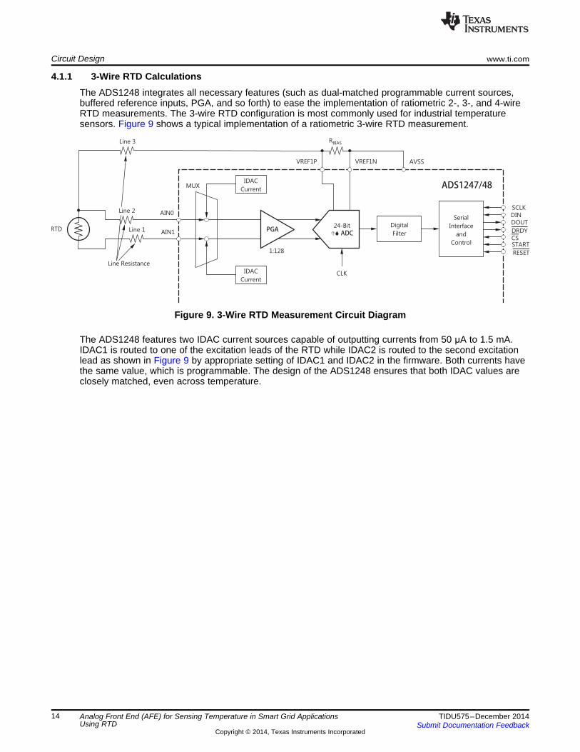
4.1.1 3-Wire RTD CalculationsThe ADS1248 integrates all necessary features (such as dual-matched programmable current sources,buffered reference inputs, PGA, and so forth) to ease the implementation of ratiometric 2-, 3-, and 4-wireRTD measurements. The 3-wire RTD configuration is most commonly used for industrial temperaturesensors. Figure 9 shows a typical implementation of a ratiometric 3-wire RTD measurement.
Figure 9. 3-Wire RTD Measurement Circuit Diagram
The ADS1248 features two IDAC current sources capable of outputting currents from 50 μA to 1.5 mA.IDAC1 is routed to one of the excitation leads of the RTD while IDAC2 is routed to the second excitationlead as shown in Figure 9 by appropriate setting of IDAC1 and IDAC2 in the firmware. Both currents havethe same value, which is programmable. The design of the ADS1248 ensures that both IDAC values areclosely matched, even across temperature.
14 Analog Front End (AFE) for Sensing Temperature in Smart Grid Applications TIDU575–December 2014Using RTD Submit Documentation Feedback
Copyright © 2014, Texas Instruments Incorporated

REFPGA
MAX
V 2VGAIN 20.6
VIN 97.04mV= = =
REFREF
V 2 VR 2 K
2 IDAC1 2 500 µA= = = W
´ ´
REF REFV 2 IDAC1 R= ´ ´
( )REF REFV IDAC1 IDAC2 R= + ´
www.ti.com Circuit Design
4.1.1.1 RREF and PGA GainThe resistance of the Pt100 changes from 80.31 Ω at –50°C to 194.07 Ω at 250°C. The line resistanceRLEAD depends on the distance of the sensor from the measurement setup. Assuming RLEAD equals 5 Ω,the positive resistance swing is from 100 to 194.07 Ω, which is about 90.07 Ω. The negative resistanceswing is from 100 to 80.31 Ω, which is about 19.69 Ω. The IDAC current must be 1 mA or less to minimizethe self-heating error. The IDAC current chosen here is 500 μA. Then, maximum and minimum inputvoltages to the PGA are 194.07 Ω × 500 μA = 97.04 mV and 80.31 Ω × 500 μA = 40.15 mV, respectively.The external reference resistor RREF serves two purposes firstly it decides the external reference voltagefor ADC and secondly, it also determines the input common mode voltage of the PGA. Set the commonmode voltage around mid-supply (AVDD – AVSS) / 2 = (3 V – 0 V) / 2 = 1.65 V. Therefore, the referencevoltage chosen here is 2 V, which also depends on easily available resistance value and excitationcurrent. The sum of both currents flows through a precision low-drift reference resistor, RREF. The voltage,VREF, generated across the reference resistor is given in Equation 5:
(5)
Because IDAC1 = IDAC2 = 500 μA:(6)
Solving for RREF:
(7)
For the required gain:
(8)
The nearest gain that can be programmed is 16.
15TIDU575–December 2014 Analog Front End (AFE) for Sensing Temperature in Smart Grid ApplicationsUsing RTDSubmit Documentation Feedback
Copyright © 2014, Texas Instruments Incorporated

( ) ( )RTDCMI LEAD LEAD REF
IDAC RV IDAC R 2 I DAC R R
2
´= ´ + + ´ ´ +
Circuit Design www.ti.com
4.1.1.2 Common-Mode Voltage Compliance CheckThe signal of an RTD is of a pseudo-differential nature, where the negative input must be biased at avoltage other than 0 V and the positive input can then swing up to 97.04 mV above the negative input.
The allowed common-mode input voltage range is as highlighted in Figure 10 (taken from the ADS1248datasheet [8]):
Figure 10. Common-Mode Input Range Equation
Assume that IDAC1 = IDAC2 and RL (RLEAD) = 5 Ω (depending on length of lead wires).
Calculating VCMI from the equations highlighted in Figure 10:Placing AVSS = 0 V, VIN = 97.04 mV, Gain = 16, and AVDD = 3.3 V in the equations shown in Figure 10:
VCMI_MIN = 0.876 V and VCMI_MAX = 2.423 V
Now, the common-mode input voltage actually set by the design can be given as:
(9)
Placing IDAC = 500 µA, RLEAD = 5 Ω, RRTD = 194.07 Ω, and RREF = 2 kΩ in Equation 9:VCMI_MIN_APPLIED = 2.027 V
Placing IDAC = 500 μA, RLEAD = 5 Ω, RRTD = 194.07 Ω, and RREF = 2 kΩ in Equation 9:VCMI_MAX_APPLIED = 2.056 V
Here, VCMI_MIN_APPLIED > VCMI_MIN and VCMI_MAX_APPLIED < VCMI_MAX
This value is well within the maximum allowed common-mode input voltage range.
16 Analog Front End (AFE) for Sensing Temperature in Smart Grid Applications TIDU575–December 2014Using RTD Submit Documentation Feedback
Copyright © 2014, Texas Instruments Incorporated

( )3dB _I_DIFFI_DIFF I1 RTD I2
3dB _I_DIFF
1F
2 C R R R
F 402.1Hz
-
-
=´ p ´ ´ + +
»
GAINΔΣ
ADC
RREF
RZERO
RRTD
I1
I2
REFP REFN
RR1 RR2
RI1
RI2
CI_CM1
CI_DIFF
CI_CM2
CR_CM1 CR_CM2CR_DIFF
www.ti.com Circuit Design
4.1.2 Noise Considerations and Input FilterRTD voltage output signals are typically in millivolt range which makes them susceptible to noise. A first-order differential and common-mode RC filter (RF1, RF2, CDIF1, CCM1, and CCM2) is placed on the ADC inputs,as well as on the reference inputs (RF3, RF4, CDIF2, CCM3, CCM4) to eliminate high-frequency noise in RTDmeasurements. For best performance, it is recommended to match the corner frequencies of the input andreference filters. More detailed information on matching the input and reference filters can be found inapplication report RTD Ratiometric Measurements and Filtering Using the ADS1148 and ADS1248.[2]
The differential filters chosen for this application were designed to have a –3-dB corner frequency at least10 times larger than the bandwidth of ADC. The selected ADS1248 sampling rate of 20 SPS results in a–3-dB bandwidth of 13.1 Hz. The cut off frequency chosen for this design is higher to account for fastersampling rate. For proper operation, the differential cutoff frequencies of the reference and input low-passfilters must be well matched. Matching the frequencies and filters can be difficult because as theresistance of the RTD changes over the span of the measurement, the filter cutoff frequency changes aswell. To mitigate this effect, the two resistors used in the input filter (RI1 and RI2) were chosen to be morethan an order of magnitude larger than the RTD. Limiting the resistors to at most 20 kΩ to keep DC offseterrors low due to input bias current.
Figure 11. Common Mode and Differential Mode Filters on RTD Input and Reference
RI1 = RI2 = 4.12 kΩ and CI_DIFF = 0.047 μF
The –3-dB cutoff frequency of differential input filter at a 186-Ω RTD resistance (at mid-scale temperature)can be calculated as given in Equation 10.
(10)
17TIDU575–December 2014 Analog Front End (AFE) for Sensing Temperature in Smart Grid ApplicationsUsing RTDSubmit Documentation Feedback
Copyright © 2014, Texas Instruments Incorporated

RTD_AINN4
RTD_AINP4
SGND1
SGND1
SGND
SGND SGND
SGND1
SGND
SGND SGND
RTD_REFP0
RTD_REFN0
RTD4_IEXC1RTD4_IEXC2
SGND
SGND
SGND
11
22
D27
P4SMA13CA
SGND1
+3.3V
+3.3V
RTD_AINP4
RTD_AINN4
RTD_REFP0
RTD_REFN0
RTD4_IEXC2 RTD4_IEXC1
3300pFC10
3300pFC9
0.033µFC12
4.12k
R54
4.12k
R55
0.047µFC34
4700pFC37
4700pFC38
11
22
D30
P4SMA13CA
11
22
D28
P4SMA13CA
11
22
D4
P4SMA13CA
1000pFC58
1000pFC56
1000pFC57
1000pFC43
2kR3
4.70k
R10
4.70k
R4
249
R52
249
R53
249
R15
249
R17
0
R9
SGND
RATIO
RATIO
0.1µF
C11
0.1µF
C13
0.1µF
C35
0.1µF
C36
D35DFLS1200-7
D36DFLS1200-7
A1
C3
K2
D9DESD1P0RFW-7
A1
C3
K2
D11DESD1P0RFW-7
A1
C3
K2
D25DESD1P0RFW-7
A1
C3
K2
D26DESD1P0RFW-7
1
2
3
4
J6
282834-4
( )3dB _R _DIFFR _DIFF R1 REF R2
3dB _R _DIFF
1F
2 C R R R
F 405.83 Hz
-
-
=´ p ´ ´ + +
»
Circuit Design www.ti.com
To ensure that mismatch of the common-mode filtering capacitors is not translated to a differential voltage,the common-mode capacitors (CI_CM1 and CI_CM2) were chosen to be 10 times smaller than the differentialcapacitor. This results in a common-mode cutoff frequency that is roughly 10 times larger than thedifferential filter, making the matching of the common-mode cutoff frequencies less critical.
CI_CM1 = CI_CM2 = 4700 pF
Although it is not always possible to exactly match the corner frequencies of all the filters, a goodcompromise is to attempt to balance the corner frequencies of the input path differential filter and thereference path differential filter because these filters have a dominant effect in the performance.
RR1 = RR2 = 4.7 kΩ and CR_DIFF = 0.033 μF
The –3-dB cutoff frequency of differential reference filter can be calculated as given in Equation 11:
(11)
To ensure that mismatch of the common-mode filtering capacitors is not translated to a differential voltage,the common-mode capacitors (CR_CM1 and CR_CM2) were chosen to be 10 times smaller than the differentialcapacitor. This results in a common-mode cutoff frequency that is roughly 10 times larger than thedifferential filter, making the matching of the common-mode cutoff frequencies less critical.
CR_CM1 = CR_CM2 = 3300 pF
Figure 12. Common-Mode and Differential-Mode Filters Implemented in Design for RTD
18 Analog Front End (AFE) for Sensing Temperature in Smart Grid Applications TIDU575–December 2014Using RTD Submit Documentation Feedback
Copyright © 2014, Texas Instruments Incorporated

5
4
1
2
3
6
7
8
1725711
J3
SGND
+3.3V
SDA
SCL 2.0kR57
2.0kR56
SDA
SCL
SDI
SDO
SCLK
TP8
RATIO
1
2
3
4
J1
282834-4
www.ti.com Circuit Design
Furthermore, before taking sensor measurement, the user must ensure that the external RC filters settledown to ½ LSB after activating the excitation current sources. It may be ensured by implementingsoftware delay for several RC time constants. For 24-bit resolution measurement, after exciting thesensor, the user must wait up to 17-RC filter time constants for consistent measurements.
Table 4. 4-Pin Terminal Block TH Connector for External RTD Input
RTD CONNECTOR ON THE BOARDRTD1 J1RTD2 J2RTD3 J4RTD4 J6
Figure 13 shows the RTD connectors on the board.
Figure 13. J1 Connector of RTD1
The ADS1248 has a simple SPI-compatible serial interface to communicate with the host. In this design,the SPI is communicating at 2Mbps.
Figure 14 shows the 8-pin terminal block for the SPI and I2C interface.
Figure 14. J3 Connector for SPI and I2C Interface With External Devices
19TIDU575–December 2014 Analog Front End (AFE) for Sensing Temperature in Smart Grid ApplicationsUsing RTDSubmit Documentation Feedback
Copyright © 2014, Texas Instruments Incorporated
1EN1
IN22
1S43
1S34
1S25
1S16
1D7
GND8
2D9
2S110
2S211
2S312
2S413
IN114
2EN15
V+16
U3
TS3A5017D
RTD1_IEXC2
IEXC2
RTD2_IEXC2
RTD3_IEXC2
RTD4_IEXC2
RTD1_IEXC1
IEXC1
RTD2_IEXC1
RTD3_IEXC1
RTD4_IEXC1
SGND
SGND
SGND
+3.3V
0.1µFC19100R37
RTD_Sel0
100R23RTD_Sel1
SGND
0R22
0R21
0R20
0R19
0R24
0R36
0R35
0R34
0R33
0R29
10µF
C20
10k
R25
10k
R38
1Logic
ControlLogic
Control
2 15
3 14
4 13
5 12
6 11
7 10
1EN
IN2
1S
1S
1S
1S
1D
4
3
2
1
GND
V
2EN
+
IN1
2S4
2S
2S
2S
2D
3
2
1
8 9
Circuit Design www.ti.com
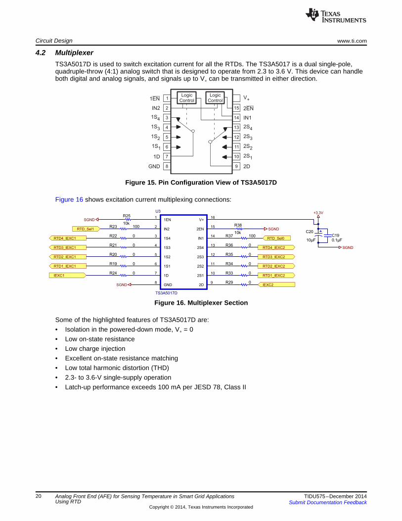
4.2 MultiplexerTS3A5017D is used to switch excitation current for all the RTDs. The TS3A5017 is a dual single-pole,quadruple-throw (4:1) analog switch that is designed to operate from 2.3 to 3.6 V. This device can handleboth digital and analog signals, and signals up to V+ can be transmitted in either direction.
Figure 15. Pin Configuration View of TS3A5017D
Figure 16 shows excitation current multiplexing connections:
Figure 16. Multiplexer Section
Some of the highlighted features of TS3A5017D are:• Isolation in the powered-down mode, V+ = 0• Low on-state resistance• Low charge injection• Excellent on-state resistance matching• Low total harmonic distortion (THD)• 2.3- to 3.6-V single-supply operation• Latch-up performance exceeds 100 mA per JESD 78, Class II
20 Analog Front End (AFE) for Sensing Temperature in Smart Grid Applications TIDU575–December 2014Using RTD Submit Documentation Feedback
Copyright © 2014, Texas Instruments Incorporated
1
2
3
4
5
6
7
8
16
15
14
13
12
11
10
9
V
ADDR
CCI
RESET
P0
P1
P2
P3
GND
V
SDA
CCP
SCL
INT
P7
P6
P5
P4
www.ti.com Circuit Design
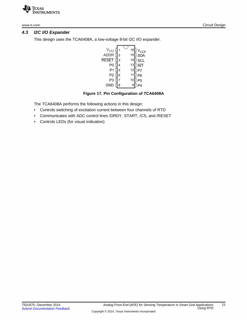
4.3 I2C I/O ExpanderThis design uses the TCA6408A, a low-voltage 8-bit I2C I/O expander.
Figure 17. Pin Configuration of TCA6408A
The TCA6408A performs the following actions in this design:• Controls switching of excitation current between four channels of RTD• Communicates with ADC control lines /DRDY, START, /CS, and /RESET• Controls LEDs (for visual indication)
21TIDU575–December 2014 Analog Front End (AFE) for Sensing Temperature in Smart Grid ApplicationsUsing RTDSubmit Documentation Feedback
Copyright © 2014, Texas Instruments Incorporated

VCCI1
ADDR2
RESET3
P04
P15
P26
P37
GND8
P49
P510
P611
P712
INT13
SCL14
SDA15
VCCP16
U2
TCA6408APWR
+3.3V
SGND
SDASCL
/INT1
RESET1
+3.3V
SGND
SDA
SCL
RE
SE
T1
RTD_Sel1
RTD_Sel0
TP3
0.1µFC17
SGND
ADC_Rdy/
ADC_Reset/10kR16
10kR11
LED1LED2
ADC_CS/ADC_Start
ADC_CS/
ADC_Start
/IN
T1
10kR27
Circuit Design www.ti.com
Figure 18. I2C I/O Expander
This 8-bit I/O expander for the I2C provides general-purpose remote I/O expansion through the I2Cinterface [serial clock (SCL) and serial data (SDA)].
Some of the highlighted features of the TCA6408A are:• Operating power-supply voltage range of 1.65 to 5.5 V• I2C to parallel port expander• Low standby current consumption of 1 μA• Schmitt-trigger action allows slow input transition and better switching noise immunity at the SCL and
SDA inputs VHYS = 0.33 V typical at 3.3 V• 5-V tolerant I/O ports• Active-low reset (RESET) input• Open-drain active-low interrupt (INT) output• 400-kHz fast I2C bus• I/O configuration register• Polarity inversion register• Internal power-on reset• Power up with all channels configured as inputs• No glitch on power up• Noise filter on SCL/SDA inputs• Latch-up performance exceeds 100 mA per JESD 78, Class II• ESD protection exceeds JESD 22
– 2000-V human-body model (A114-A)– 1000-V charged-device model (C101)
22 Analog Front End (AFE) for Sensing Temperature in Smart Grid Applications TIDU575–December 2014Using RTD Submit Documentation Feedback
Copyright © 2014, Texas Instruments Incorporated

OUT1
DNC2
PG3
4
EN5
NC6
DELAY7
IN8
9
EP GND
U1TPS7A1633DGNR
0.1µFC154.7µF
C16
L1
1000 OHM
TP4+3.3V
SGNDSGNDSGND
3.8V
D14PTZTE253.6B
SGND
SGND
SGND
1000pF
C50.1µFC8
SGND
+6V TP1
10µF
C4 1.2kR26
0R14
10µF
C14
GreenD13
IN
DELAY
NC
EN
OUT
FB/DNC
PG
GND
1
2
3
4
8
7
6
5
www.ti.com Circuit Design
4.4 Power SupplyThe TPS7A1633 is an ultra-low power, LDO voltage regulator that offers the benefits of ultra-lowquiescent current, high input voltage and miniaturized, high thermal-performance packaging.
The TPS7A1633 is designed for continuous or sporadic (power backup) battery-powered applicationswhere ultra-low quiescent current is critical to extending system battery life.
The TPS7A1633 offers an enable pin (EN) compatible with standard CMOS logic and an integrated opendrain active-high power good output (PG) with a user-programmable delay. These pins are intended foruse in microcontroller-based, battery-powered applications where power-rail sequencing is required.
Not only can this device supply a well-regulated voltage rail, but it can also withstand and maintainregulation during voltage transients. These features translate to simpler and more cost-effective, electricalsurge-protection circuitry
Table 5. Critical Parameters of TPS7A1633
PARAMETER VALUEIout (Max) (A) 0.1Output options Fixed outputVin (Min) (V) 3Vin (Max) (V) 60
Fixed output options (V) 3.3Vout (Min) (V) 3.3Vout (Max) (V) 3.3Iq (Typ) (mA) 0.005
Vdo (Typ) (mV) 60Accuracy (%) 2
PSRR at 100 KHz (dB) 26
Figure 19. Pin Configuration of TPS7A1633
Figure 20 shows the implementation of a 3.3-V power supply using the TPS7A1633 LDO.
Figure 20. TPS7A1633 Section of the TIDA-00110 Schematic
23TIDU575–December 2014 Analog Front End (AFE) for Sensing Temperature in Smart Grid ApplicationsUsing RTDSubmit Documentation Feedback
Copyright © 2014, Texas Instruments Incorporated
SGND
TP10TP9+6V
1
2
3
4
J5
282834-4
Circuit Design www.ti.com
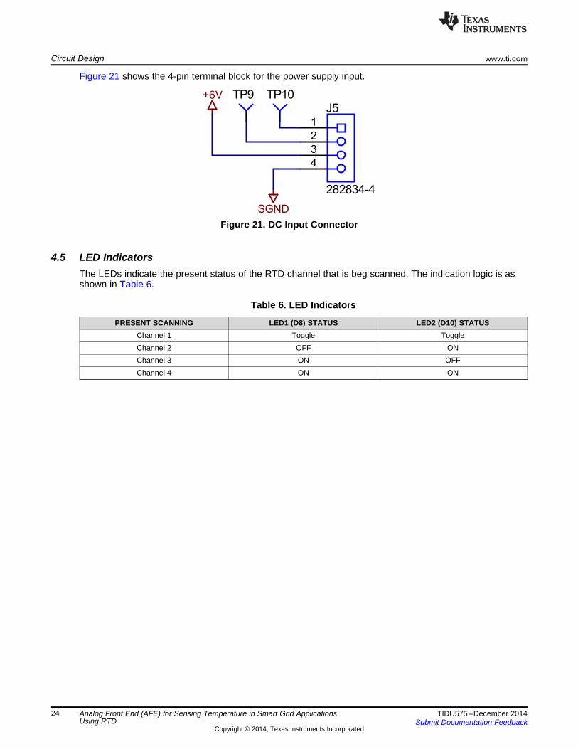
Figure 21 shows the 4-pin terminal block for the power supply input.
Figure 21. DC Input Connector
4.5 LED IndicatorsThe LEDs indicate the present status of the RTD channel that is beg scanned. The indication logic is asshown in Table 6.
Table 6. LED Indicators
PRESENT SCANNING LED1 (D8) STATUS LED2 (D10) STATUSChannel 1 Toggle ToggleChannel 2 OFF ONChannel 3 ON OFFChannel 4 ON ON
24 Analog Front End (AFE) for Sensing Temperature in Smart Grid Applications TIDU575–December 2014Using RTD Submit Documentation Feedback
Copyright © 2014, Texas Instruments Incorporated
Power SelectSwitch Green Power LED
USB Connector(Power/ICDI)
Reset Switch
RGB User LED
User Switch 2User Switch 1
USB Micro-A/-BConnector(Device)
Tiva C SeriesLaunchPadBoosterPack XLInterface (J1, J2, J3,and J4 Connectors)
Tiva C SeriesLaunchPadBoosterPack XLInterface (J1, J2, J3,and J4 Connectors)
MSP430LaunchPad-CompatibleBoosterPack Interface
MSP430LaunchPad-CompatibleBoosterPack Interface
TivaTM4C123GH6PMIMicrocontroller
TivaTM4C123GH6PMIMicrocontroller
www.ti.com Circuit Design
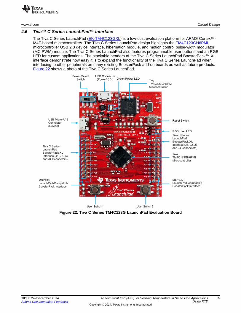
4.6 Tiva™ C Series LaunchPad™ InterfaceThe Tiva C Series LaunchPad (EK-TM4C123GXL) is a low-cost evaluation platform for ARM® Cortex™-M4F-based microcontrollers. The Tiva C Series LaunchPad design highlights the TM4C123GH6PMImicrocontroller USB 2.0 device interface, hibernation module, and motion control pulse-width modulator(MC PWM) module. The Tiva C Series LaunchPad also features programmable user buttons and an RGBLED for custom applications. The stackable headers of the Tiva C Series LaunchPad BoosterPack™ XLinterface demonstrate how easy it is to expand the functionality of the Tiva C Series LaunchPad wheninterfacing to other peripherals on many existing BoosterPack add-on boards as well as future products.Figure 22 shows a photo of the Tiva C Series LaunchPad.
Figure 22. Tiva C Series TM4C123G LaunchPad Evaluation Board
25TIDU575–December 2014 Analog Front End (AFE) for Sensing Temperature in Smart Grid ApplicationsUsing RTDSubmit Documentation Feedback
Copyright © 2014, Texas Instruments Incorporated

Circuit Design www.ti.com
4.7 PCB Design Guidelines• An SMD ceramic bypass capacitor of approximately 0.1 μF in value is recommended for all the digital
ICs. Should it be required to use leaded components, keep leads as short as possible to minimize leadinductance.
• A continuous ground plane is ideal for providing a low-impedance signal return path as well asgenerating the lowest EMI signature by reducing phenomena such as unintended current loops.
• Should a continuous ground plane not be possible, it is important to minimize the length of the traceconnecting VCC and ground.
• PCB material: Standard Flame Retardant 4 (FR-4) epoxy-glass as printed-circuit board (PCB) materialis preferred for industrial applications with a speed < 100 Mhz. FR-4 meets the requirements ofUnderwriters Laboratories UL94-V0 and is preferred over cheaper alternatives due to its lowerdielectric losses at high frequencies, less moisture absorption, greater strength and stiffness, and itsself-extinguishing, flammability characteristics.
• Trace routing: Use 45° bends (chamfered corners), instead of right-angle (90°) bends. Right-anglebends increase the effective trace width, and thus the trace impedance. This creates additionalimpedance mismatch, which may lead to higher reflections.
26 Analog Front End (AFE) for Sensing Temperature in Smart Grid Applications TIDU575–December 2014Using RTD Submit Documentation Feedback
Copyright © 2014, Texas Instruments Incorporated

RTD2 RTD3
RT
D4
6 V
GN
D
SPI and I2C
RT
D1
www.ti.com Software Description
5 Software DescriptionFor software description and code examples for TIDA-00110, please see TIDU575: Software CodeExamples for TIDA-00110.
6 Test SetupTools and equipment used to test ADC measurement accuracy:• Yokogawa Model GS610 Source Measure Unit with accuracy: ±0.02% (DC voltage generation)• Agilent 34401A 6½-Digit Multimeter for measuring resistance in four-wire method and measuring mV• 0.01% tolerance high precision resistor to simulate RTD resistance
Figure 23. Test Setup for TIDA-00110
For Pt100 RTD, Table 7 shows resistance and respective voltage (mV) for different temperatures.
Table 7. Temperature versus Voltage Across RTD
TEMPERATURE (°C) RESISTANCE (Ω) EXPECTED VOLTAGE DROP WITH 500-µA EXCITATION CURRENT (mV)–50 80.3068 40.15
0 100.0000 50.0050 119.3951 59.70100 138.5000 69.25150 157.3149 78.66200 175.8396 87.92250 194.0743 97.04
27TIDU575–December 2014 Analog Front End (AFE) for Sensing Temperature in Smart Grid ApplicationsUsing RTDSubmit Documentation Feedback
Copyright © 2014, Texas Instruments Incorporated
( )( )
( )REF DEC
IN DEC 23
2 V ADC _ CODEV 1 LSB ADC _ CODE
GAIN 2 1
´ ´= ´ =
´ -
Test Results www.ti.com
7 Test Results
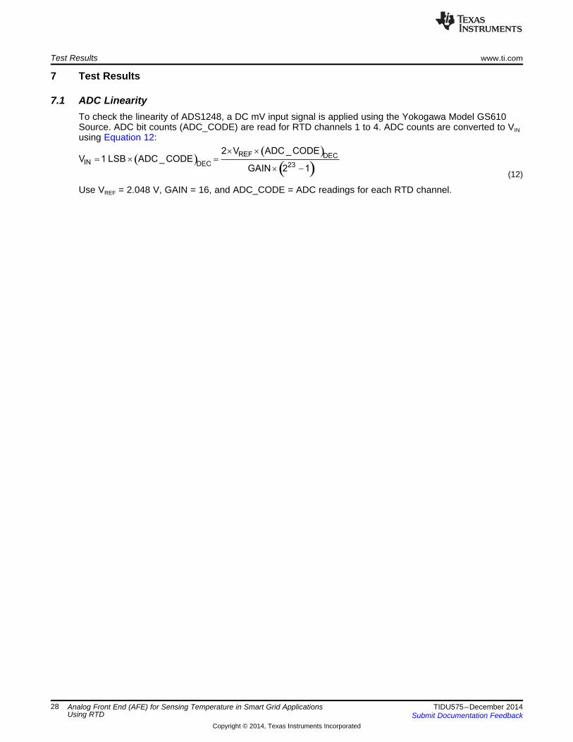
7.1 ADC LinearityTo check the linearity of ADS1248, a DC mV input signal is applied using the Yokogawa Model GS610Source. ADC bit counts (ADC_CODE) are read for RTD channels 1 to 4. ADC counts are converted to VINusing Equation 12:
(12)
Use VREF = 2.048 V, GAIN = 16, and ADC_CODE = ADC readings for each RTD channel.
28 Analog Front End (AFE) for Sensing Temperature in Smart Grid Applications TIDU575–December 2014Using RTD Submit Documentation Feedback
Copyright © 2014, Texas Instruments Incorporated

www.ti.com Test Results
Table 8. Channel 1: Linearity Performance
VCHANNEL1 (mV) CHANNEL1ERRORVAPPLIED (mV) (WITHOUT GAIN MULTIPLICATION) (AFTER GAIN MULTIPLICATION)24.972 24.95766 0.07%29.972 29.94252 0.03%34.969 34.9265 0.01%36.969 36.92699 0.01%38.970 38.9221 0.01%40.969 40.92225 0.01%42.969 42.9146 0.00%44.969 44.90884 –0.01%46.968 46.91064 0.01%48.967 48.90668 0.01%50.970 50.90246 0.00%52.970 52.89703 –0.01%54.967 54.89291 –0.01%56.968 56.88804 –0.01%58.967 58.885 –0.01%60.968 60.88195 –0.01%62.967 62.87782 –0.01%64.966 64.87613 –0.01%69.965 69.86636 –0.01%74.965 74.85669 –0.02%79.964 79.85213 –0.01%84.963 84.84324 –0.01%89.963 89.83919 –0.01%94.963 94.835 –0.01%96.960 96.83171 0.00%99.960 99.82369 –0.01%102.962 102.8255 0.00%105.962 105.8196 –0.01%107.960 107.8193 0.00%109.960 109.8188 0.00%111.959 111.8131 0.00%114.958 114.8095 0.00%119.957 119.8032 0.00%124.957 124.7988 0.00%126.958 126.7952 0.00%129.956 128.0000 –1.38%
NOTE: Applied gain multiplication factor is 1.00128.
29TIDU575–December 2014 Analog Front End (AFE) for Sensing Temperature in Smart Grid ApplicationsUsing RTDSubmit Documentation Feedback
Copyright © 2014, Texas Instruments Incorporated

Test Results www.ti.com
Table 9. Channel 2: Linearity Performance
VCHANNEL2 (mV) CHANNEL2ERRORVAPPLIED (mV) (WITHOUT GAIN MULTIPLICATION) (AFTER GAIN MULTIPLICATION)24.972 24.95338 0.06%29.972 29.93974 0.02%34.969 34.92714 0.01%36.969 36.92403 0.01%38.970 38.91727 0.00%40.969 40.91727 0.00%42.969 42.91207 0.00%44.969 44.90584 –0.01%46.968 46.91152 0.01%48.967 48.90452 0.00%50.970 50.89978 –0.01%52.970 52.89782 –0.01%54.967 54.8893 –0.01%56.968 56.88943 –0.01%58.967 58.88457 –0.01%60.968 60.88365 –0.01%62.967 62.87493 –0.02%64.966 64.87406 –0.01%69.965 69.86466 –0.01%74.965 74.85849 –0.01%79.964 79.85144 –0.01%84.963 84.8479 0.00%89.963 89.83695 –0.01%94.963 94.83193 –0.01%96.960 96.82842 0.00%99.960 99.82069 –0.01%102.962 102.822 –0.01%105.962 105.8159 –0.01%107.960 107.8166 0.00%109.960 109.8165 0.00%111.959 111.8078 0.00%114.958 114.8069 0.00%119.957 119.8038 0.00%124.957 124.7929 0.00%126.958 126.7918 0.00%129.956 128.0000 –1.38%
NOTE: Applied gain factor is 1.001310.
30 Analog Front End (AFE) for Sensing Temperature in Smart Grid Applications TIDU575–December 2014Using RTD Submit Documentation Feedback
Copyright © 2014, Texas Instruments Incorporated

www.ti.com Test Results
Table 10. Channel 3: Linearity Performance
VCHANNEL3 (mV) CHANNEL3ERRORVAPPLIED (mV) (WITHOUT GAIN MULTIPLICATION) (AFTER GAIN MULTIPLICATION)24.972 24.95697 0.07%29.972 29.94044 0.02%34.969 34.92873 0.01%36.969 36.92693 0.01%38.970 38.92284 0.01%40.969 40.91598 0.00%42.969 42.91109 –0.01%44.969 44.90875 –0.01%46.968 46.90954 0.00%48.967 48.9026 0.00%50.970 50.9006 –0.01%52.970 52.89588 –0.01%54.967 54.89344 –0.01%56.968 56.88652 –0.01%58.967 58.88598 –0.01%60.968 60.88221 –0.01%62.967 62.87755 –0.01%64.966 64.8734 –0.01%69.965 69.86158 –0.02%74.965 74.85734 –0.02%79.964 79.8507 –0.01%84.963 84.84557 –0.01%89.963 89.8371 –0.01%94.963 94.83109 –0.01%96.960 96.83072 –0.01%99.960 99.82227 –0.01%102.962 102.8224 –0.01%105.962 105.8192 –0.01%107.960 107.8165 0.00%109.960 109.8157 0.00%111.959 111.8106 0.00%114.958 114.8075 0.00%119.957 119.8013 0.00%124.957 124.7962 0.00%126.958 126.7951 0.00%129.956 128.0000 –1.38%
NOTE: Applied gain factor is 1.001284.
31TIDU575–December 2014 Analog Front End (AFE) for Sensing Temperature in Smart Grid ApplicationsUsing RTDSubmit Documentation Feedback
Copyright © 2014, Texas Instruments Incorporated

Test Results www.ti.com
Table 11. Channel 4: Linearity Performance
VCHANNEL4 (mV) CHANNEL4ERRORVAPPLIED (mV) (WITHOUT GAIN MULTIPLICATION) (AFTER GAIN MULTIPLICATION)24.972 24.95606 0.07%29.972 29.94122 0.03%34.969 34.92886 0.01%36.969 36.92489 0.01%38.970 38.92012 0.00%40.969 40.91657 0.00%42.969 42.91369 0.00%44.969 44.90719 –0.01%46.968 46.9107 0.01%48.967 48.90607 0.00%50.970 50.90158 –0.01%52.970 52.89598 –0.01%54.967 54.89154 –0.01%56.968 56.88658 –0.01%58.967 58.88463 –0.01%60.968 60.88013 –0.02%62.967 62.87574 –0.02%64.966 64.87512 –0.01%69.965 69.86325 –0.02%74.965 74.85668 –0.02%79.964 79.85253 –0.01%84.963 84.8452 –0.01%89.963 89.8364 –0.01%94.963 94.83339 –0.01%96.960 96.83004 0.00%99.960 99.82408 –0.01%102.962 102.8224 –0.01%105.962 105.8189 –0.01%107.960 107.8186 0.00%109.960 109.814 0.00%111.959 111.8099 0.00%114.958 114.8075 0.00%119.957 119.7999 0.00%124.957 124.796 0.00%126.958 126.7941 0.00%129.956 128.0000 –1.38%
NOTE: Applied gain factor is 1.001292.
32 Analog Front End (AFE) for Sensing Temperature in Smart Grid Applications TIDU575–December 2014Using RTD Submit Documentation Feedback
Copyright © 2014, Texas Instruments Incorporated

VAPPLIED (mV)
Err
or
20 40 60 80 100 120 140-1.5%
-1.2%
-0.9%
-0.6%
-0.3%
0
0.3%
D001
Channel1ERROR (%)Channel2ERROR (%)Channel3ERROR (%)Channel4ERROR (%)
www.ti.com Test Results
When an 130-mV input is applied, for a gain of 16 the output is 2080 mV. The ADC range up to which thelinearity performance is guaranteed is 2048 mV. The ADC measurement saturates above 2048 mV.
Figure 24. ADC Linearity Performance After Applying Gain Factor
33TIDU575–December 2014 Analog Front End (AFE) for Sensing Temperature in Smart Grid ApplicationsUsing RTDSubmit Documentation Feedback
Copyright © 2014, Texas Instruments Incorporated

Test Results www.ti.com
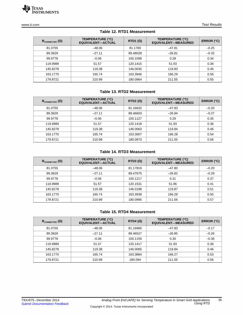
7.2 ADS1248 Characterization in Temperature Measurement ConfigurationTo test the accuracy of the acquisition circuit alone, a series of high-precision discrete resistors were usedas the input to the system. The offset error can be attributed largely due to the offset of the internal PGAand ADC, while the gain error can be attributed to the accuracy of the RREF resistor and gain error of theinternal PGA and ADC. The ADC error characterization includes corrections for any mismatch in excitationcurrents, offset, and gain errors.
Figure 25. 4-Wire Resistance Measurement Using 6½-Digit Multimeter
The design team followed this procedure for ADD characterization:1. Chose different resistor values representing the RTD temperature inputs2. Selected the resistance range equivalent to the temperature range of interest3. Combined multiple resistors in series and parallel to get the required resistance values4. Measured the resistance values with a multi-meter using the 4-wire resistance measurement technique5. Connected the resistors to the RTD input terminals with care to ensure there was no additional
resistance being introduced from the contact by tightening the screws6. Used a GUI to display the measured values
34 Analog Front End (AFE) for Sensing Temperature in Smart Grid Applications TIDU575–December 2014Using RTD Submit Documentation Feedback
Copyright © 2014, Texas Instruments Incorporated
www.ti.com Test Results
Table 12. RTD1 Measurement
TEMPERATURE (°C) TEMPERATURE (°C)RCONNECTED (Ω) RTD1 (Ω) ERROR (°C)EQUIVALENT—ACTUAL EQUIVALENT—MEASURED81.0755 –48.06 81.1769 –47.81 –0.2589.3629 –27.11 89.48028 –26.81 –0.3299.9778 –0.06 100.1098 0.28 0.34119.9989 51.57 120.1415 51.93 0.36145.8278 119.38 146.0030 119.83 0.45163.1770 165.74 163.3946 166.29 0.56179.8721 210.99 180.0964 211.55 0.55
Table 13. RTD2 Measurement
TEMPERATURE (°C) TEMPERATURE (°C)RCONNECTED (Ω) RTD2 (Ω) ERROR (°C)EQUIVALENT—ACTUAL EQUIVALENT—MEASURED81.0755 –48.06 81.16632 –47.83 –0.2089.3629 –27.11 89.46603 –26.84 –0.2799.9778 –0.06 100.1127 0.29 0.35119.9989 51.57 120.1418 51.93 0.36145.8278 119.38 146.0063 119.84 0.46163.1770 165.74 163.3907 166.28 0.54179.8721 210.99 180.0973 211.55 0.56
Table 14. RTD3 Measurement
TEMPERATURE (°C) TEMPERATURE (°C)RCONNECTED (Ω) RTD3 (Ω) ERROR (°C)EQUIVALENT—ACTUAL EQUIVALENT—MEASURED81.0755 –48.06 81.17819 –47.80 –0.2089.3629 –27.11 89.47675 –26.82 –0.2999.9778 –0.06 100.1217 0.31 0.37119.9989 51.57 120.1531 51.96 0.41145.8278 119.38 146.0188 119.87 0.51163.1770 165.74 163.3938 166.29 0.55179.8721 210.99 180.0995 211.56 0.57
Table 15. RTD4 Measurement
TEMPERATURE (°C) TEMPERATURE (°C)RCONNECTED (Ω) RTD4 (Ω) ERROR (°C)EQUIVALENT—ACTUAL EQUIVALENT—MEASURED81.0755 –48.06 81.16966 –47.83 –0.1789.3629 –27.11 89.46527 –26.85 –0.2699.9778 –0.06 100.1159 0.30 –0.36119.9989 51.57 120.1417 51.93 0.36145.8278 119.38 146.0065 119.84 0.46163.1770 165.74 163.3884 166.27 0.53179.8721 210.99 180.094 211.55 0.56
35TIDU575–December 2014 Analog Front End (AFE) for Sensing Temperature in Smart Grid ApplicationsUsing RTDSubmit Documentation Feedback
Copyright © 2014, Texas Instruments Incorporated

Temperature (°C) Equivalent of the Connected Resistor
Err
or (
°C)
-60 -30 0 30 60 90 120 150 180 210 240-0.4
-0.3
-0.2
-0.1
0
0.1
0.2
0.3
0.4
0.5
0.6
D002
RTD1ERROR (°C)RTD2ERROR (°C)RTD3ERROR (°C)RTD4ERROR (°C)
Test Results www.ti.com
Figure 26 shows error for the four RTS after multiplying the measured mV with gain factor.
Figure 26. RTD Measurement Accuracy
7.3 Interfacing With Isolated Synchronous Serial Communication Module (TIDA-00300)This design is a sub-system for sensing multiple RTD channels inside a protection relay or an RTDexpansion module. For safety in some of the applications, the RTD inputs are isolated from the measuringsystem. This design, when interfaced with the Isolated Synchronous Serial Communication Module(TIDA-00300) is configured as an isolated RTD measurement module. TIDA-00300 provides isolation forSPI, I2C, and DC voltage inputs. The interface connectors are simple screw-type connectors enablingeasy connection between the two boards.
Isolated RTD functionality is verified with the TIDA-00300 board.
Table 16. Summary
SERIAL NUMBER TITLE OBSERVATION1 Sensing of RTD inputs ADC measured the inputs as expected2 ADC, PGA configuration Measurement follows the programmed gain3 I2C I/O expander All I/Os functions were as expected
36 Analog Front End (AFE) for Sensing Temperature in Smart Grid Applications TIDU575–December 2014Using RTD Submit Documentation Feedback
Copyright © 2014, Texas Instruments Incorporated
RTD_AINN1
RTD_AINP1
SGND1
SGND1
SGND
SGND SGND
RTD1_IEXC1
D5DFLS1200-7
RTD1_IEXC2
0.1µF
C6
SGND
11
22
D3
P4SMA13CA
SGND1
+3.3V
RTD_AINP1
RTD_AINN1
RTD1_IEXC2 RTD1_IEXC1
4.12k
R2
4.12k
R1
0.047µFC1
4700pFC3
4700pFC2
A1
C3
K2
D6DESD1P0RFW-7
11
22
D1
P4SMA13CA
11
22
D2
P4SMA13CA1000pF
C411000pF
C40
1000pFC42
RTD_AINN2
RTD_AINP2
SGND1
SGND1
SGND
SGND SGND
RTD2_IEXC1RTD2_IEXC2
SGND
11
22
D12
P4SMA13CA
SGND1
+3.3V
RTD_AINP2
RTD_AINN2
RTD2_IEXC2 RTD2_IEXC1
4.12k
R28
4.12k
R30
0.047µFC23
4700pFC21
4700pFC22
11
22
D19
P4SMA13CA
11
22
D15
P4SMA13CA1000pF
C471000pF
C49
1000pFC46
RTD_AINN3
RTD_AINP3
SGND1
SGND1
SGND
SGND SGND
RTD3_IEXC1RTD3_IEXC2
SGND
11
22
D20
P4SMA13CA
SGND1
+3.3V
RTD_AINP3
RTD_AINN3
RTD3_IEXC2 RTD3_IEXC1
4.12k
R45
4.12k
R51
0.047µFC30
4700pFC28
4700pFC32
11
22
D23
P4SMA13CA
11
22
D21
P4SMA13CA1000pF
C531000pF
C54
1000pFC51
249
R5
249
R6
249
R31
249
R32
249
R48
249
R49
RATIO
RATIO
RATIO
1
2
3
4
J1
282834-4
RATIO
0.1µF
C7
0.1µF
C18
0.1µF
C24
0.1µF
C27
0.1µF
C33
D18DFLS1200-7
D31DFLS1200-7
D32DFLS1200-7
D33DFLS1200-7
D34DFLS1200-7
A1
C3
K2
D7DESD1P0RFW-7
A1
C3
K2
D16DESD1P0RFW-7
A1
C3
K2
D17DESD1P0RFW-7
A1
C3
K2
D22DESD1P0RFW-7
A1
C3
K2
D24DESD1P0RFW-7
1
2
3
4
J2
282834-4
1
2
3
4
J4
282834-4
www.ti.com Design Files
8 Design Files
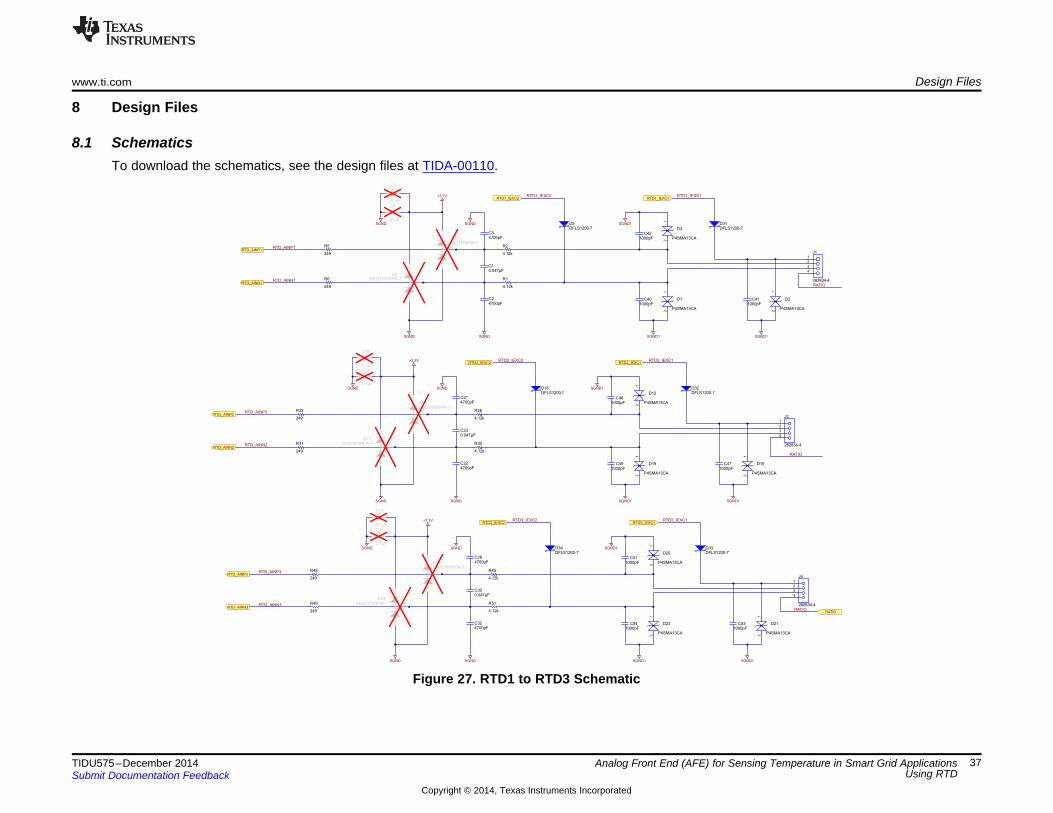
8.1 SchematicsTo download the schematics, see the design files at TIDA-00110.
Figure 27. RTD1 to RTD3 Schematic
37TIDU575–December 2014 Analog Front End (AFE) for Sensing Temperature in Smart Grid ApplicationsUsing RTDSubmit Documentation Feedback
Copyright © 2014, Texas Instruments Incorporated

RTD_AINN4
RTD_AINP4
SGND1
SGND1
SGND
SGND SGND
SGND1
SGND
SGND SGND
RTD_REFP0
RTD_REFN0
RTD4_IEXC1RTD4_IEXC2
SGND
SGND
SGND
11
22
D27
P4SMA13CA
SGND1
+3.3V
+3.3V
RTD_AINP4
RTD_AINN4
RTD_REFP0
RTD_REFN0
RTD4_IEXC2 RTD4_IEXC1
3300pFC10
3300pFC9
0.033µFC12
4.12k
R54
4.12k
R55
0.047µFC34
4700pFC37
4700pFC38
11
22
D30
P4SMA13CA
11
22
D28
P4SMA13CA
11
22
D4
P4SMA13CA
1000pFC58
1000pFC56
1000pFC57
1000pFC43
2kR3
4.70k
R10
4.70k
R4
249
R52
249
R53
249
R15
249
R17
0
R9
SGND
SMBJ18CA
D29
SGND1
Chessis ground
1000pF
C55
1000pF
C39
1
2
J7
282834-2
RATIO
RATIO
0.1µF
C11
0.1µF
C13
0.1µF
C35
0.1µF
C36
D35DFLS1200-7
D36DFLS1200-7
A1
C3
K2
D9DESD1P0RFW-7
A1
C3
K2
D11DESD1P0RFW-7
A1
C3
K2
D25DESD1P0RFW-7
A1
C3
K2
D26DESD1P0RFW-7
1
2
3
4
J6
282834-4
Design Files www.ti.com
Figure 28. RTD4 and Ratiometric Measurement
38 Analog Front End (AFE) for Sensing Temperature in Smart Grid Applications TIDU575–December 2014Using RTD Submit Documentation Feedback
Copyright © 2014, Texas Instruments Incorporated

DVDD1
DGND2
CLK3
RESET4
REFP0/GPIO05
REFN0/GPIO16
REFP17
REFN18
VREFOUT9
VREFCOM10
AIN0/IEXC11
AIN1/IEXC12
AIN4/IEXC/GPIO413
AIN5/IEXC/GPIO514
AIN6/IEXC/GPIO615
AIN7/IEXC/GPIO716
AIN2/IEXC/GPIO217
AIN3/IEXC/GPIO318
IOUT219
IOUT120
AVSS21
AVDD22
START23
CS24
DRDY25
DOUT/DRDY26
DIN27
SCLK28
U4
ADS1248IPW
1EN1
IN22
1S43
1S34
1S25
1S16
1D7
GND8
2D9
2S110
2S211
2S312
2S413
IN114
2EN15
V+16
U3
TS3A5017D
RTD_AINN4
RTD_AINP4
RTD_AINN3
RTD_AINP3
IEXC2
IEXC1
RTD_AINP1
RTD_AINN1
RTD_AINP2
RTD_AINN2
RTD1_IEXC2
IEXC2
RTD2_IEXC2
RTD3_IEXC2
RTD4_IEXC2
RTD1_IEXC1
IEXC1
RTD2_IEXC1
RTD3_IEXC1
RTD4_IEXC1
RTD_REFP0
RTD_REFN0
SGND
SGND
+3.3V
+3.3V100
R44
100
R43
100
R47
100
R42
SCLK
SDO
SDI
SGND
+3.3V
0.1µFC52
+3.3V
0.1µF
C29
SGND
0.1µFC50
100R40
100R39
TP7
TP6
SGND
SGND
SGND
+3.3V
0.1µFC19100R37
RTD_Sel0
100R23RTD_Sel1
5
4
1
2
3
6
7
8
1725711
J3
SGND
+3.3V
SDASCL
ADC_Rdy/
SGND
0R22
0R21
0R20
0R19
0R24
0R36
0R35
0R34
0R33
0R29
ADC_CS/
ADC_Start
ADC_Reset/
RESET12.0kR57
2.0kR56
SDA
SCL/INT1
TP2 TP5
SGND
SGND
SDISDOSCLK
TP8
10µF
C20
10µF
C26
10µF
C31
10µF
C48
0.1µFC25 10kR46
10kR50
10kR18
10k
R25
10k
R38
10kR41
www.ti.com Design Files
Figure 29. ADS1248 and Analog Switch Circuit
39TIDU575–December 2014 Analog Front End (AFE) for Sensing Temperature in Smart Grid ApplicationsUsing RTDSubmit Documentation Feedback
Copyright © 2014, Texas Instruments Incorporated

VCCI1
ADDR2
RESET3
P04
P15
P26
P37
GND8
P49
P510
P611
P712
INT13
SCL14
SDA15
VCCP16
U2
TCA6408APWR
+3.3V
SGND
SDASCL
/INT1
RESET1
+3.3V
SGND
SDA
SCL
RE
SE
T1
RTD_Sel1
RTD_Sel0
TP3
0.1µFC17
SGND
ADC_Rdy/
ADC_Reset/
OUT1
DNC2
PG3
4
EN5
NC6
DELAY7
IN8
9
EP GND
U1TPS7A1633DGNR
0.1µFC154.7µF
C16
L1
1000 OHM
TP4+3.3V
SGNDSGNDSGND
3.8V
D14PTZTE253.6B
SGND
SGND
SGND
1000pF
C50.1µFC8
SGND
+6V
10kR16
10kR11
300
R13
0.1µFC45
SGND
30V
3
264
1 587
Q2
CSD17571Q2300
R7
0.1µFC44
SGND
30V
3
264
1 587
Q1
CSD17571Q2LED1 LED2
GreenD8
+3.3V+3.3V
300R8
300R12
LED1LED2
SGND
ADC_CS/ADC_Start
ADC_CS/
ADC_Start
/IN
T1
TP10TP9
TP1
10µF
C4 1.2kR26
0R14
+6V
10µF
C14
GreenD10
GreenD13
1
2
3
4
J5
282834-410kR27
Design Files www.ti.com
Figure 30. I2C I/O Expander, Power Supply, and LEDs
40 Analog Front End (AFE) for Sensing Temperature in Smart Grid Applications TIDU575–December 2014Using RTD Submit Documentation Feedback
Copyright © 2014, Texas Instruments Incorporated
www.ti.com Design Files
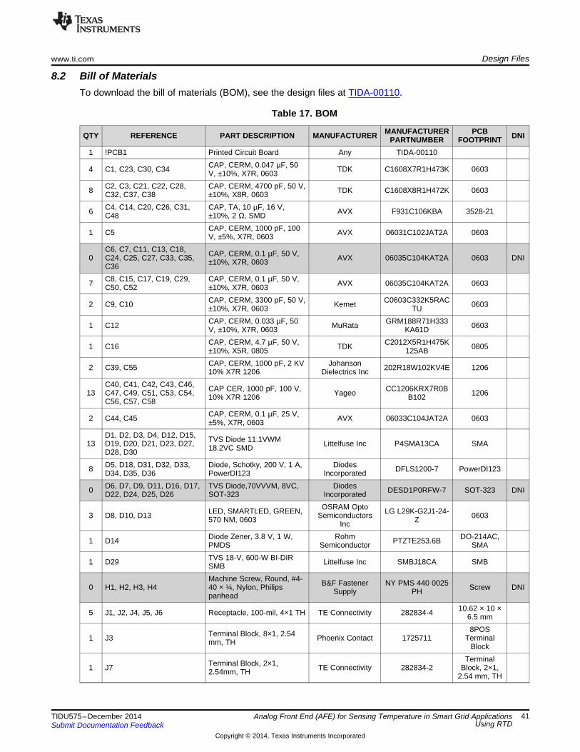
8.2 Bill of MaterialsTo download the bill of materials (BOM), see the design files at TIDA-00110.
Table 17. BOM
MANUFACTURER PCBQTY REFERENCE PART DESCRIPTION MANUFACTURER DNIPARTNUMBER FOOTPRINT1 !PCB1 Printed Circuit Board Any TIDA-00110
CAP, CERM, 0.047 µF, 504 C1, C23, C30, C34 TDK C1608X7R1H473K 0603V, ±10%, X7R, 0603C2, C3, C21, C22, C28, CAP, CERM, 4700 pF, 50 V,8 TDK C1608X8R1H472K 0603C32, C37, C38 ±10%, X8R, 0603C4, C14, C20, C26, C31, CAP, TA, 10 µF, 16 V,6 AVX F931C106KBA 3528-21C48 ±10%, 2 Ω, SMD
CAP, CERM, 1000 pF, 1001 C5 AVX 06031C102JAT2A 0603V, ±5%, X7R, 0603C6, C7, C11, C13, C18, CAP, CERM, 0.1 µF, 50 V,0 C24, C25, C27, C33, C35, AVX 06035C104KAT2A 0603 DNI±10%, X7R, 0603C36C8, C15, C17, C19, C29, CAP, CERM, 0.1 µF, 50 V,7 AVX 06035C104KAT2A 0603C50, C52 ±10%, X7R, 0603
CAP, CERM, 3300 pF, 50 V, C0603C332K5RAC2 C9, C10 Kemet 0603±10%, X7R, 0603 TUCAP, CERM, 0.033 µF, 50 GRM188R71H3331 C12 MuRata 0603V, ±10%, X7R, 0603 KA61DCAP, CERM, 4.7 µF, 50 V, C2012X5R1H475K1 C16 TDK 0805±10%, X5R, 0805 125ABCAP, CERM, 1000 pF, 2 KV Johanson2 C39, C55 202R18W102KV4E 120610% X7R 1206 Dielectrics Inc
C40, C41, C42, C43, C46, CAP CER, 1000 pF, 100 V, CC1206KRX7R0B13 C47, C49, C51, C53, C54, Yageo 120610% X7R 1206 B102C56, C57, C58CAP, CERM, 0.1 µF, 25 V,2 C44, C45 AVX 06033C104JAT2A 0603±5%, X7R, 0603
D1, D2, D3, D4, D12, D15, TVS Diode 11.1VWM13 D19, D20, D21, D23, D27, Littelfuse Inc P4SMA13CA SMA18.2VC SMDD28, D30D5, D18, D31, D32, D33, Diode, Schotky, 200 V, 1 A, Diodes8 DFLS1200-7 PowerDI123D34, D35, D36 PowerDI123 IncorporatedD6, D7, D9, D11, D16, D17, TVS Diode,70VVVM, 8VC, Diodes0 DESD1P0RFW-7 SOT-323 DNID22, D24, D25, D26 SOT-323 Incorporated
OSRAM OptoLED, SMARTLED, GREEN, LG L29K-G2J1-24-3 D8, D10, D13 Semiconductors 0603570 NM, 0603 ZIncDiode Zener, 3.8 V, 1 W, Rohm DO-214AC,1 D14 PTZTE253.6BPMDS Semiconductor SMATVS 18-V, 600-W BI-DIR1 D29 Littelfuse Inc SMBJ18CA SMBSMBMachine Screw, Round, #4- B&F Fastener NY PMS 440 00250 H1, H2, H3, H4 40 × ¼, Nylon, Philips Screw DNISupply PHpanhead
10.62 × 10 ×5 J1, J2, J4, J5, J6 Receptacle, 100-mil, 4×1 TH TE Connectivity 282834-4 6.5 mm8POSTerminal Block, 8×1, 2.541 J3 Phoenix Contact 1725711 Terminalmm, TH Block
TerminalTerminal Block, 2×1,1 J7 TE Connectivity 282834-2 Block, 2×1,2.54mm, TH 2.54 mm, TH
41TIDU575–December 2014 Analog Front End (AFE) for Sensing Temperature in Smart Grid ApplicationsUsing RTDSubmit Documentation Feedback
Copyright © 2014, Texas Instruments Incorporated

Design Files www.ti.com
Table 17. BOM (continued)MANUFACTURER PCBQTY REFERENCE PART DESCRIPTION MANUFACTURER DNIPARTNUMBER FOOTPRINT
Ferrite Chip 1000 Ω, 3001 L1 TDK Corporation MMZ1608B102C 0603MA, 0603Thermal Transfer Printable PCB Label
0 LBL1 Labels, 0.650" W × 0.200" H Brady THT-14-423-10 0.650"H × DNI- 10,000 per roll 0.200"WMOSFET, N-CH, 30 V, 22 A,2 Q1, Q2 Texas Instruments CSD17571Q2 DQKSON 2X2 MM
R1, R2, R28, R30, R45, RES, 4.12 kΩ, 0.1%, 0.1 W, RG1608P-4121-B-8 Susumu Co Ltd 0603R51, R54, R55 0603 T5TNPW12062K00B1 R3 RES 2 KΩ, ¼ W, 0.1% 1206 Vishay-Dale 1206EEA
RES, 4.70 kΩ, 0.1%, 0.1 W, RG1608P-472-B-2 R4, R10 Susumu Co Ltd 06030603 T5R5, R6, R15, R17, R31, CRCW0603249RF10 RES, 249, 1%, 0.1 W, 0603 Vishay-Dale 0603R32, R48, R49, R52, R53 KEA
RES, 300 Ω, 5%, 0.1 W, CRCW0603300RJ4 R7, R8, R12, R13 Vishay-Dale 06030603 NEARES, 0 Ω, 5%, 0.125 W,1 R9 Yageo America RC0805JR-070RL 08050805
CRCW060310K0J0 R11, R46, R50 RES, 10 k, 5%, 0.1 W, 0603 Vishay-Dale 0603 DNINEACRCW06030000Z00 R14 RES, 0, 5%, 0.1 W, 0603 Vishay-Dale 0603 DNIEA
R16, R18, R25, R27, R38, CRCW060310K0J6 RES, 10 k, 5%, 0.1 W, 0603 Vishay-Dale 0603R41 NEAR19, R20, R21, R22, R24, CRCW06030000Z010 RES, 0, 5%, 0.1 W, 0603 Vishay-Dale 0603R29, R33, R34, R35, R36 EAR23, R37, R39, R40, R42, CRCW0603100RF8 RES, 100, 1%, 0.1 W, 0603 Vishay-Dale 0603R43, R44, R47 KEA
CRCW06031K20J1 R26 RES, 1.2 k, 5%, 0.1 W, 0603 Vishay-Dale 0603NEAHP2 R56, R57 RES, 2.0 k, 5%, 0.1 W, 0603 Yageo America RC0603JR-072KL 0603
TP1, TP2, TP3, TP4, TP5, Test Point 40-mil pad, 20-mil10 STD STDTP6, TP7, TP8, TP9, TP10 drillSingle Output LDO, 100 mA,Fixed 3.3-V Output, 3- to 60-V Input, with Enable and1 U1 Texas Instruments TPS7A1633DGNR DGN0008CPower Good, 8-pin MSOP(DGN), –40°C to 125°C,Green (RoHS and no Sb/Br)Low-Voltage 8-Bit I2C andSMBus I/O Expander, 1.65
1 U2 to 5.5 V, –40°C to 85°C, 16- Texas Instruments TCA6408APWR PW0016Apin TSSOP (PW), Green(RoHS and no Sb/Br)IC, Dual, 14 Ω, SP4T Analog1 U3 Texas Instruments TS3A5017D SO16SwitchIC, 24-Bit A-D Converters for1 U4 Texas Instruments ADS1248IPW TSSOP-28Temperature Sensors
42 Analog Front End (AFE) for Sensing Temperature in Smart Grid Applications TIDU575–December 2014Using RTD Submit Documentation Feedback
Copyright © 2014, Texas Instruments Incorporated

www.ti.com Design Files
8.3 Layer PlotsTo download the layer plots, see the design files at TIDA-00110.
Figure 31. Top Overlay Figure 32. Top Solder
Figure 33. Top Layer Figure 34. GND Plane
Figure 35. PWR Plane Figure 36. Bottom Layer
43TIDU575–December 2014 Analog Front End (AFE) for Sensing Temperature in Smart Grid ApplicationsUsing RTDSubmit Documentation Feedback
Copyright © 2014, Texas Instruments Incorporated
Design Files www.ti.com
Figure 37. Bottom Solder Figure 38. Bottom Overlay
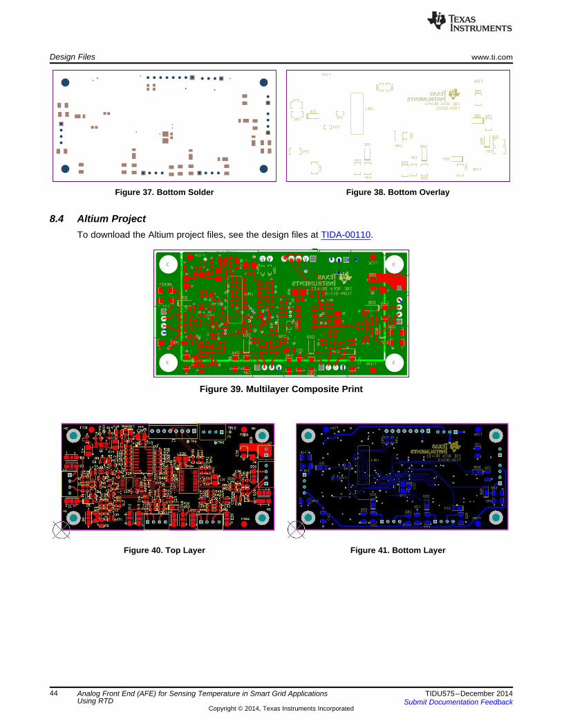
8.4 Altium ProjectTo download the Altium project files, see the design files at TIDA-00110.
Figure 39. Multilayer Composite Print
Figure 40. Top Layer Figure 41. Bottom Layer
44 Analog Front End (AFE) for Sensing Temperature in Smart Grid Applications TIDU575–December 2014Using RTD Submit Documentation Feedback
Copyright © 2014, Texas Instruments Incorporated

www.ti.com Design Files
8.5 Gerber FilesTo download the Gerber files, see the design files at TIDA-00110.
Figure 42. Fabrication Drawing
45TIDU575–December 2014 Analog Front End (AFE) for Sensing Temperature in Smart Grid ApplicationsUsing RTDSubmit Documentation Feedback
Copyright © 2014, Texas Instruments Incorporated

Design Files www.ti.com
8.6 Assembly Drawings
Figure 43. Top Assembly Drawing Figure 44. Bottom Assembly Drawing
8.7 Software FilesTo download the software files, see the design files at TIDA-00110.
9 References
1. Texas Instruments, RTD Temperature Transmitter for 2-Wire, 4 to 20-mA Current Loop Systems,TIDA-00095 Design Guide (TIDU182)
2. Texas Instruments, RTD Ratiometric Measurements and Filtering Using the ADS1148 and ADS1248Family of Devices Application Report (SBAA201)
3. TI Precision, Hardware-Compensated Ratiometric 3-Wire RTD System, 0°C – 100°C, 0.005°C ErrorDesign Guide (TIDU045)
4. TI Precision, 3-Wire RTD Measurement System Reference Design, –200°C to 850°C (SLAU520)5. Robert Burnham and Nagaraj Ananthapadamanabhan, Example Temperature Measurement
Applications Using the ADS1247 and ADS1248, Application Report (SBAA180)6. Collin Wells, Signal Conditioning and Linearization of RTD Sensors, 2011 Texas Instruments
Technology Day Presentation (TIDU433)7. Texas Instruments, Advanced Debugging Using the Enhanced Emulation Module (EEM) With Code
Composer Studio Version 6, Application Report (SLAA393)8. Texas Instruments, 24-Bit Analog-to-Digital Converters for Temperature Sensors, ADS1248 Datasheet
(SBAS426G)
10 About the AuthorPRAHLAD SUPEDA is a systems engineer at Texas Instruments India where he is responsible fordeveloping reference design solutions for Smart Grid within Industrial Systems. Prahlad brings to this rolehis extensive experience in power electronics, EMC, analog, and mixed signal designs. Prahlad earnedhis bachelor of instrumentation and control engineering from Nirma University, India. He can be reachedat [email protected].
VIVEK GOPALAKRISHNAN is a firmware architect at Texas Instruments India where he is responsiblefor developing reference design solutions for Smart Grid within Industrial Systems. Vivek brings to his rolehis experience in firmware architecture design and development. Vivek earned his master’s degree insensor systems technology from VIT University, India. He can be reached at [email protected].
46 Analog Front End (AFE) for Sensing Temperature in Smart Grid Applications TIDU575–December 2014Using RTD Submit Documentation Feedback
Copyright © 2014, Texas Instruments Incorporated

IMPORTANT NOTICE FOR TI REFERENCE DESIGNS
Texas Instruments Incorporated ("TI") reference designs are solely intended to assist designers (“Buyers”) who are developing systems thatincorporate TI semiconductor products (also referred to herein as “components”). Buyer understands and agrees that Buyer remainsresponsible for using its independent analysis, evaluation and judgment in designing Buyer’s systems and products.TI reference designs have been created using standard laboratory conditions and engineering practices. TI has not conducted anytesting other than that specifically described in the published documentation for a particular reference design. TI may makecorrections, enhancements, improvements and other changes to its reference designs.Buyers are authorized to use TI reference designs with the TI component(s) identified in each particular reference design and to modify thereference design in the development of their end products. HOWEVER, NO OTHER LICENSE, EXPRESS OR IMPLIED, BY ESTOPPELOR OTHERWISE TO ANY OTHER TI INTELLECTUAL PROPERTY RIGHT, AND NO LICENSE TO ANY THIRD PARTY TECHNOLOGYOR INTELLECTUAL PROPERTY RIGHT, IS GRANTED HEREIN, including but not limited to any patent right, copyright, mask work right,or other intellectual property right relating to any combination, machine, or process in which TI components or services are used.Information published by TI regarding third-party products or services does not constitute a license to use such products or services, or awarranty or endorsement thereof. Use of such information may require a license from a third party under the patents or other intellectualproperty of the third party, or a license from TI under the patents or other intellectual property of TI.TI REFERENCE DESIGNS ARE PROVIDED "AS IS". TI MAKES NO WARRANTIES OR REPRESENTATIONS WITH REGARD TO THEREFERENCE DESIGNS OR USE OF THE REFERENCE DESIGNS, EXPRESS, IMPLIED OR STATUTORY, INCLUDING ACCURACY ORCOMPLETENESS. TI DISCLAIMS ANY WARRANTY OF TITLE AND ANY IMPLIED WARRANTIES OF MERCHANTABILITY, FITNESSFOR A PARTICULAR PURPOSE, QUIET ENJOYMENT, QUIET POSSESSION, AND NON-INFRINGEMENT OF ANY THIRD PARTYINTELLECTUAL PROPERTY RIGHTS WITH REGARD TO TI REFERENCE DESIGNS OR USE THEREOF. TI SHALL NOT BE LIABLEFOR AND SHALL NOT DEFEND OR INDEMNIFY BUYERS AGAINST ANY THIRD PARTY INFRINGEMENT CLAIM THAT RELATES TOOR IS BASED ON A COMBINATION OF COMPONENTS PROVIDED IN A TI REFERENCE DESIGN. IN NO EVENT SHALL TI BELIABLE FOR ANY ACTUAL, SPECIAL, INCIDENTAL, CONSEQUENTIAL OR INDIRECT DAMAGES, HOWEVER CAUSED, ON ANYTHEORY OF LIABILITY AND WHETHER OR NOT TI HAS BEEN ADVISED OF THE POSSIBILITY OF SUCH DAMAGES, ARISING INANY WAY OUT OF TI REFERENCE DESIGNS OR BUYER’S USE OF TI REFERENCE DESIGNS.TI reserves the right to make corrections, enhancements, improvements and other changes to its semiconductor products and services perJESD46, latest issue, and to discontinue any product or service per JESD48, latest issue. Buyers should obtain the latest relevantinformation before placing orders and should verify that such information is current and complete. All semiconductor products are soldsubject to TI’s terms and conditions of sale supplied at the time of order acknowledgment.TI warrants performance of its components to the specifications applicable at the time of sale, in accordance with the warranty in TI’s termsand conditions of sale of semiconductor products. Testing and other quality control techniques for TI components are used to the extent TIdeems necessary to support this warranty. Except where mandated by applicable law, testing of all parameters of each component is notnecessarily performed.TI assumes no liability for applications assistance or the design of Buyers’ products. Buyers are responsible for their products andapplications using TI components. To minimize the risks associated with Buyers’ products and applications, Buyers should provideadequate design and operating safeguards.Reproduction of significant portions of TI information in TI data books, data sheets or reference designs is permissible only if reproduction iswithout alteration and is accompanied by all associated warranties, conditions, limitations, and notices. TI is not responsible or liable forsuch altered documentation. Information of third parties may be subject to additional restrictions.Buyer acknowledges and agrees that it is solely responsible for compliance with all legal, regulatory and safety-related requirementsconcerning its products, and any use of TI components in its applications, notwithstanding any applications-related information or supportthat may be provided by TI. Buyer represents and agrees that it has all the necessary expertise to create and implement safeguards thatanticipate dangerous failures, monitor failures and their consequences, lessen the likelihood of dangerous failures and take appropriateremedial actions. Buyer will fully indemnify TI and its representatives against any damages arising out of the use of any TI components inBuyer’s safety-critical applications.In some cases, TI components may be promoted specifically to facilitate safety-related applications. With such components, TI’s goal is tohelp enable customers to design and create their own end-product solutions that meet applicable functional safety standards andrequirements. Nonetheless, such components are subject to these terms.No TI components are authorized for use in FDA Class III (or similar life-critical medical equipment) unless authorized officers of the partieshave executed an agreement specifically governing such use.Only those TI components that TI has specifically designated as military grade or “enhanced plastic” are designed and intended for use inmilitary/aerospace applications or environments. Buyer acknowledges and agrees that any military or aerospace use of TI components thathave not been so designated is solely at Buyer's risk, and Buyer is solely responsible for compliance with all legal and regulatoryrequirements in connection with such use.TI has specifically designated certain components as meeting ISO/TS16949 requirements, mainly for automotive use. In any case of use ofnon-designated products, TI will not be responsible for any failure to meet ISO/TS16949.IMPORTANT NOTICE
Mailing Address: Texas Instruments, Post Office Box 655303, Dallas, Texas 75265Copyright © 2014, Texas Instruments Incorporated