an4570 application note - home - … application note considers a 16-bit asynchronous nor flash...
TRANSCRIPT
January 2015 DocID026804 Rev 1 1/461
AN4570Application note
Using the high-density STM32F30xxD/E FMC peripheral to drive external memories
IntroductionThis application note describes how to use the high-density STM32F30xxD/E FMC (flexible memory controller) peripheral to drive a set of external memories. For that aim, it gives an overview of the STM32F30xxD/E FMC. The document also presents memory interfacing examples that include the typical FMC configuration, the timing computation method and the hardware connection.
This application note considers a 16-bit asynchronous NOR Flash memory, an 8-bit NAND Flash memory and a 16-bit asynchronous SRAM.
The STM32F30xxD/E firmware library and the different memory drivers corresponding to the memory types presented in this application note are available for download on STMicroelectronics website at www.st.com.
Table 1 provides the list of products to which this application note applies.
Table 1. Applicable productsReference Part number
STM32F30xxD/E
STM32F302RD, STM32F302VD, STM32F302ZD,STM32F302RE, STM32F302VE, STM32F302ZE,STM32F303RD, STM32F303VD, STM32F303ZD,STM32F303RE, STM32F303VE, STM32F303ZE.
www.st.com

Contents AN4570
2/46 DocID026804 Rev 1
Contents
1 Overview of the STM32F30xxD/E flexible static memory controller . . 51.1 Interfacing asynchronous static memories (NOR Flash, SRAM) . . . . . . . . 7
2 Interfacing with a non-multiplexed, asynchronous 16-bit NOR Flash memory . . . . . . . . . . . . . . . . . . . . . . . . . . . . . . . . . . . . 92.1 FMC configuration . . . . . . . . . . . . . . . . . . . . . . . . . . . . . . . . . . . . . . . . . . . 9
2.1.1 Typical use of the FMC to interface with a NOR Flash memory . . . . . . 10
2.2 Timing computation . . . . . . . . . . . . . . . . . . . . . . . . . . . . . . . . . . . . . . . . . 11
2.3 Hardware connection . . . . . . . . . . . . . . . . . . . . . . . . . . . . . . . . . . . . . . . . 13
3 Interfacing with a non-multiplexed, asynchronous 16-bit SRAM . . . . 223.1 FMC configuration . . . . . . . . . . . . . . . . . . . . . . . . . . . . . . . . . . . . . . . . . . 22
3.1.1 Typical use of the FMC to interface with an SRAM . . . . . . . . . . . . . . . . 23
3.2 Timing computation . . . . . . . . . . . . . . . . . . . . . . . . . . . . . . . . . . . . . . . . . 23
3.3 Hardware connection . . . . . . . . . . . . . . . . . . . . . . . . . . . . . . . . . . . . . . . . 24
4 Interfacing with an 8-bit NAND Flash memory . . . . . . . . . . . . . . . . . . . 304.1 FMC configuration . . . . . . . . . . . . . . . . . . . . . . . . . . . . . . . . . . . . . . . . . . 31
4.1.1 Typical use of the FMC to interface with a NAND memory . . . . . . . . . . 32
4.2 Timing computation . . . . . . . . . . . . . . . . . . . . . . . . . . . . . . . . . . . . . . . . . 33
4.3 Hardware connection . . . . . . . . . . . . . . . . . . . . . . . . . . . . . . . . . . . . . . . . 35
4.4 Error correction code computation . . . . . . . . . . . . . . . . . . . . . . . . . . . . . . 414.4.1 Error correction code (ECC) computation overview . . . . . . . . . . . . . . . 41
4.4.2 Error detection . . . . . . . . . . . . . . . . . . . . . . . . . . . . . . . . . . . . . . . . . . . . 41
5 STM32F30xxD/E FMC configuration in 100-pin packages . . . . . . . . . . 435.1 Interfacing the FMC with a NAND Flash memory . . . . . . . . . . . . . . . . . . 43
5.2 Interfacing the FMC with a NOR Flash memory . . . . . . . . . . . . . . . . . . . . 44
6 Revision history . . . . . . . . . . . . . . . . . . . . . . . . . . . . . . . . . . . . . . . . . . . 45
DocID026804 Rev 1 3/46
AN4570 List of tables
3
List of tables
Table 1. Applicable products. . . . . . . . . . . . . . . . . . . . . . . . . . . . . . . . . . . . . . . . . . . . . . . . . . . . . . . . 1Table 2. FMC operating modes . . . . . . . . . . . . . . . . . . . . . . . . . . . . . . . . . . . . . . . . . . . . . . . . . . . . . 7Table 3. STM32F30xxD/E FMC asynchronous timings . . . . . . . . . . . . . . . . . . . . . . . . . . . . . . . . . . . 8Table 4. NOR Flash memory timings . . . . . . . . . . . . . . . . . . . . . . . . . . . . . . . . . . . . . . . . . . . . . . . . 12Table 5. M29W128FL signal to FMC pin correspondence . . . . . . . . . . . . . . . . . . . . . . . . . . . . . . . . 13Table 6. IS61WV51216BL SRAM timings. . . . . . . . . . . . . . . . . . . . . . . . . . . . . . . . . . . . . . . . . . . . . 24Table 7. IS61WV51216BLL signal to FMC pin correspondence. . . . . . . . . . . . . . . . . . . . . . . . . . . . 24Table 8. NAND512W3A2C Flash memory timings . . . . . . . . . . . . . . . . . . . . . . . . . . . . . . . . . . . . . . 34Table 9. NAND512W3A signal to FMC pin correspondence . . . . . . . . . . . . . . . . . . . . . . . . . . . . . . 35Table 10. NAND Flash memory connection to the FMC. . . . . . . . . . . . . . . . . . . . . . . . . . . . . . . . . . . 43Table 11. NOR Flash memory connection to the FMC. . . . . . . . . . . . . . . . . . . . . . . . . . . . . . . . . . . . 44Table 12. Document revision history. . . . . . . . . . . . . . . . . . . . . . . . . . . . . . . . . . . . . . . . . . . . . . . . . . 45

List of figures AN4570
4/46 DocID026804 Rev 1
List of figures
Figure 1. FMC block diagram. . . . . . . . . . . . . . . . . . . . . . . . . . . . . . . . . . . . . . . . . . . . . . . . . . . . . . . . 6Figure 2. FMC memory banks . . . . . . . . . . . . . . . . . . . . . . . . . . . . . . . . . . . . . . . . . . . . . . . . . . . . . . . 7Figure 3. Asynchronous NOR Flash read access timing . . . . . . . . . . . . . . . . . . . . . . . . . . . . . . . . . . 10Figure 4. Asynchronous NOR Flash write access timing. . . . . . . . . . . . . . . . . . . . . . . . . . . . . . . . . . 10Figure 5. 16-bit NOR Flash: M29W128FL/GL connection to STM32F30xxD/E. . . . . . . . . . . . . . . . . 14Figure 6. SRAM asynchronous read access timing . . . . . . . . . . . . . . . . . . . . . . . . . . . . . . . . . . . . . . 22Figure 7. SRAM asynchronous write access timing. . . . . . . . . . . . . . . . . . . . . . . . . . . . . . . . . . . . . . 23Figure 8. 16-bit SRAM: IS61WV51216BLL connection to STM32F30xxD/E . . . . . . . . . . . . . . . . . . . 25Figure 9. FMC NAND bank sections . . . . . . . . . . . . . . . . . . . . . . . . . . . . . . . . . . . . . . . . . . . . . . . . . 30Figure 10. NAND memory access timing. . . . . . . . . . . . . . . . . . . . . . . . . . . . . . . . . . . . . . . . . . . . . . . 32Figure 11. 8-bit NAND Flash: NAND512W3A2C/NAND512W3A2B connection to STM32F30xxD/E . 36Figure 12. Error detection flowchart . . . . . . . . . . . . . . . . . . . . . . . . . . . . . . . . . . . . . . . . . . . . . . . . . . . 41
DocID026804 Rev 1 5/46
AN4570 Overview of the STM32F30xxD/E flexible static memory controller
45
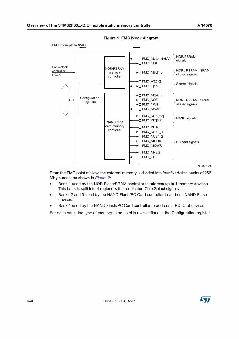
1 Overview of the STM32F30xxD/E flexible static memory controller
The FMC has the following main features:• Interface with static-memory mapped devices including:
– Static random access memory (SRAM),– NOR Flash memory/OneNAND Flash memory,– PSRAM (4 memory banks),– 16-bit PC Card compatible devices,– Two banks of NAND Flash memory with ECC hardware to check up to 8 Kbyte of
data• Supports burst mode access to synchronous devices (NOR Flash and PSRAM)• 8- or 16-bit wide data bus• Independent chip select control for each memory bank• Independent configuration for each memory bank• Programmable timings to support a wide range of devices, in particular:
– Programmable wait states (up to 15)– Programmable bus turnaround cycles (up to 15)– Programmable output enable and write enable delays (up to 15)– Independent read and write timings and protocol, so as to support the widest
variety of memories and timings• Write enable and byte lane select outputs for use with PSRAM and SRAM devices• Translation of 32-bit wide AHB transactions into consecutive 16-bit or 8-bit accesses to
external 16-bit or 8-bit devices• The FMC embeds two Write FIFOs:
– Write Data FIFO with 16x33-bit depth,– Write Address FIFO with 16x30-bit depth).
• External asynchronous wait control
The FMC registers that define the external device type and associated characteristics are usually set at boot time and do not change until the next reset or power-up. However, it is possible to change the settings at any time.
Figure 1 illustrates the FMC block diagram.
Overview of the STM32F30xxD/E flexible static memory controller AN4570
6/46 DocID026804 Rev 1
Figure 1. FMC block diagram
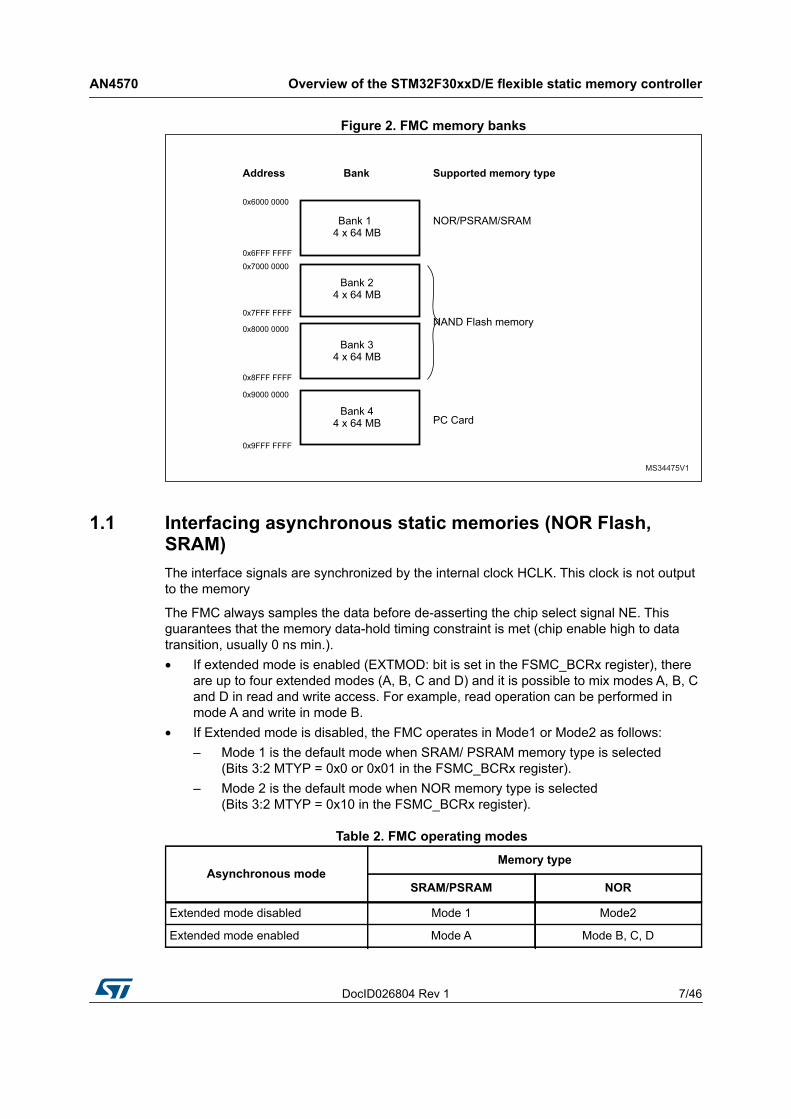
From the FMC point of view, the external memory is divided into four fixed-size banks of 256 Mbyte each, as shown in Figure 2:• Bank 1 used by the NOR Flash/SRAM controller to address up to 4 memory devices.
This bank is split into 4 regions with 4 dedicated Chip Select signals.• Banks 2 and 3 used by the NAND Flash/PC Card controller to address NAND Flash
devices.• Bank 4 used by the NAND Flash/PC Card controller to address a PC Card device.
For each bank, the type of memory to be used is user-defined in the Configuration register.
DocID026804 Rev 1 7/46
AN4570 Overview of the STM32F30xxD/E flexible static memory controller
45
Figure 2. FMC memory banks
1.1 Interfacing asynchronous static memories (NOR Flash, SRAM)The interface signals are synchronized by the internal clock HCLK. This clock is not output to the memory
The FMC always samples the data before de-asserting the chip select signal NE. This guarantees that the memory data-hold timing constraint is met (chip enable high to data transition, usually 0 ns min.).• If extended mode is enabled (EXTMOD: bit is set in the FSMC_BCRx register), there
are up to four extended modes (A, B, C and D) and it is possible to mix modes A, B, C and D in read and write access. For example, read operation can be performed in mode A and write in mode B.
• If Extended mode is disabled, the FMC operates in Mode1 or Mode2 as follows: – Mode 1 is the default mode when SRAM/ PSRAM memory type is selected
(Bits 3:2 MTYP = 0x0 or 0x01 in the FSMC_BCRx register).– Mode 2 is the default mode when NOR memory type is selected
(Bits 3:2 MTYP = 0x10 in the FSMC_BCRx register).
Table 2. FMC operating modes
Asynchronous modeMemory type
SRAM/PSRAM NOR
Extended mode disabled Mode 1 Mode2
Extended mode enabled Mode A Mode B, C, D

Overview of the STM32F30xxD/E flexible static memory controller AN4570
8/46 DocID026804 Rev 1
Note: These timings extracted from STM32F30xxD/E datasheet are needed to compute the NOR and SRAM asynchronous mode timings.
Table 3. STM32F30xxD/E FMC asynchronous timings Symbols Parameter Value Unit
HCLK Internal AHB clock frequency 72 MHz
tHCLK Internal AHB clock cycle 13.88 ns
tsu(Data_NE) + tv(A_NE)Data to FSMC_NEx high setup time + FSMC_NEx low to FSMC_A valid 1tHCLK + 9 ns

DocID026804 Rev 1 9/46
AN4570 Interfacing with a non-multiplexed, asynchronous 16-bit NOR Flash memory
45
2 Interfacing with a non-multiplexed, asynchronous 16-bit NOR Flash memory
2.1 FMC configurationTo control a NOR Flash memory, the FMC provides the following possible features:• Select the bank to be used to map the NOR Flash memory: there are 4 independent
banks which can be used to interface with NOR Flash/SRAM/PSRAM memories, each bank has a separate Chip Select pin.
• Enable or disable the address/data multiplexing feature• Select the memory type to be used: NOR Flash/SRAM/PSRAM• Define the external memory data bus width: 8/16 bits• Enable or disable the burst access mode for synchronous NOR Flash memories• Configure the use of the wait signal: enable/disable, polarity setting and timing
configuration.• Enable or disable the extended mode: this mode is used to access the memory with a
different timing configuration for read and write operations.
As the NOR Flash/PSRAM controller can support asynchronous and synchronous memories, the user should select only the used parameters depending on the memory characteristics.
The FMC also provides the possibility of programming several parameters to correctly interface with the external memory. Depending on the memory type, some parameters are not used.
In the case where an external asynchronous non-multiplexed memory is used, the user has to compute and set the following parameters depending on the information in the memory datasheet:• ADDSET: address setup time• DATAST: data setup time• ACCMOD: access mode
This parameter gives the FMC the flexibility to access a wide variety of asynchronous static memories. There are four extended access modes (A, B, C and D) that allow write access while reading the memory with different timings, if the memory supports this kind of feature.When the extended mode is enabled, the FMC_BTRx register is used for read operations and the FMC_BWTRx register is used for write operations.
In the case where a synchronous memory is used, the user has to compute and set the following parameters:• CLKDIV: clock divide ratio• DATLAT: data latency
Note that NOR Flash memory read operations can be synchronous if the memory supports this mode, while write operations usually remain asynchronous.
When programming a synchronous NOR Flash memory, the memory automatically switches between the synchronous and the asynchronous mode, so in this case, all parameters have to be set correctly.
Interfacing with a non-multiplexed, asynchronous 16-bit NOR Flash memory AN4570
10/46 DocID026804 Rev 1
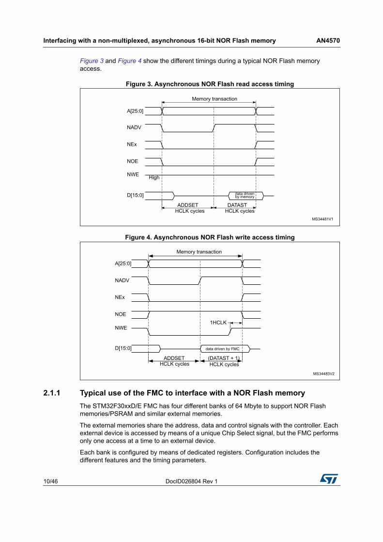
Figure 3 and Figure 4 show the different timings during a typical NOR Flash memory access.
Figure 3. Asynchronous NOR Flash read access timing
Figure 4. Asynchronous NOR Flash write access timing
2.1.1 Typical use of the FMC to interface with a NOR Flash memoryThe STM32F30xxD/E FMC has four different banks of 64 Mbyte to support NOR Flash memories/PSRAM and similar external memories.
The external memories share the address, data and control signals with the controller. Each external device is accessed by means of a unique Chip Select signal, but the FMC performs only one access at a time to an external device.
Each bank is configured by means of dedicated registers. Configuration includes the different features and the timing parameters.
DocID026804 Rev 1 11/46
AN4570 Interfacing with a non-multiplexed, asynchronous 16-bit NOR Flash memory
45
In this application note, the M29W128FL memory is used as a reference. The M29W128FL memory is a 16-bit, asynchronous, non-multiplexed NOR Flash memory. Based on these data, the FMC is configured as follows:
Bank 2 is selected to support the NOR Flash memory device:• Bank 2 is enabled: BCR2_MBKEN bit set to ‘1’• Memory type is NOR: BCR2_MTYP is set to ‘10’ to select the NOR memory type• Data bus width is 16-bit: BCR2_MWID is set to ‘01’ to select the 16-bit width• It is a non-multiplexed memory: BCR2_MUXEN is reset.
All remaining parameters must be kept cleared.
2.2 Timing computationAs described above, for asynchronous NOR Flash-like memories, there are different possible access protocols. The first step is therefore to define the kind of protocol that should be used with the specific memory. The choice depends on the different control signals and the behavior of the memory during read and write transactions.
In the case of an asynchronous NOR Flash memory, the Mode2 protocol will be used. If the used memory can provide an NADV signal, the Extended Mode B protocol should be used.
With the M29W128FL, we will use the Mode2 protocol. We will therefore not use any extended mode and the timings will be the same for read and write operations. In this case, the NOR memory controller needs two timing parameters: ADDSET and DATAST.
These parameters are computed according to the NOR Flash memory characteristics and according to the HCLK clock of the STM32F30xxD/E.
Based on the NOR Flash memory access timings illustrated in Figure 3 and Figure 4, the following equations are found:• The write or read access time is the time between the falling edge and the rising edge
of the memory Chip Select signal. This time is computed as a function of the FMC timing parameter:((ADDSET + 1) + (DATAST + 1)) × tHCLK ≥ Write access time
• In write operations, the DATAST parameter is measured between the falling edge and the rising edge of the write signal as follows:tWP = DATAST × tHCLK ≥ Write Enable signal low to high
To have a correct configuration of the FMC timings, the timings have to take into account:• the maximum read/write access time• the different internal FMC delays• the different internal memory delays
Hence, we have:((ADDSET + 1) + (DATAST + 1)) × tHCLK = max (tWC)DATAST × HCLK = tWP
For read access, DATAST must verify:DATAST ≥ (tAVQV + tsu(Data_NE) + tv(A_NE))/tHCLK – ADDSET – 4
Table 4 gives the meanings and values of the NOR Flash memory parameters.
Interfacing with a non-multiplexed, asynchronous 16-bit NOR Flash memory AN4570
12/46 DocID026804 Rev 1
Using the memory timings in Table 4 and the FMC asynchronous timings in Table 3, we can compute the following values:• For the M29W128 NOR Flash memory, the timings are:
– Address setup time: 0x0– Data setup time: 0x3
• For the S29GL128P NOR Flash memory, the timings are:– Address setup time: 0x2– Data setup time: 0x3
Note: The S29GL128P NOR Flash memory timings are also valid for the M29W128 NOR Flash memory.
Table 4. NOR Flash memory timings
Symbols ParameterValue
UnitM29W128xx70 S29GL128P90
tWCAddress valid to next address valid for write operation 70 90 ns
tRCAddress valid to next address valid for read access 70 90 ns
tWP Write Enable low to Write Enable high 45 35 ns
tAVQV Address valid to output valid 70 90 ns

DocID026804 Rev 1 13/46
AN4570 Interfacing with a non-multiplexed, asynchronous 16-bit NOR Flash memory
45
2.3 Hardware connectionTable 5 gives the correspondence between the NOR Flash memory pins and the FMC pins and shows the GPIO configuration for each FMC pin.
In case of an 8-bit NOR Flash memory, the data/address bus is 8-bit wide and D8-D15 should not be connected to the FMC. The unused FMC pins can be used for general purpose I/O.
In case of a synchronous memory, the FSMC_CLK pin should be connected to the memory clock pin.
Figure 5 shows a typical connection between an STM32F30xxD/E microcontroller and the M29W128FL NOR Flash memory.
Table 5. M29W128FL signal to FMC pin correspondence Memory signals
FMC signals Pin / Port assignment Pin / Port
configuration Signal description
A0-A22 A0-A22 Port F/Port G/Port E/Port D/PortH AF push-pull Address A0-A22
DQ0-DQ7 D0-D7 Port D/Port E AF push-pull Data D0-D7
DQ8-DQ14 D8-D14 Port D/Port E AF push-pull Data D8-D14
DQ15A-1 D15 PD10 AF push-pull Data D15
E NE2 PG9 AF push-pull Chip Enable
G NOE PD4 AF push-pull Output Enable
W NWE PD5 AF push-pull Write Enable

Interfacing with a non-multiplexed, asynchronous 16-bit NOR Flash memory AN4570
14/46 DocID026804 Rev 1
Figure 5. 16-bit NOR Flash: M29W128FL/GL connection to STM32F30xxD/E
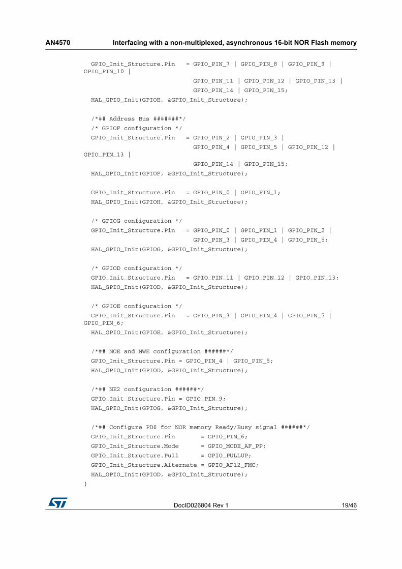
Note: The GPIO PD6 pin is used to provide a Ready/Busy output signal for NOR Flash memories (in this case the application needs to poll on the state of this pin to guarantee correct operation). In the example shown below, this pin is not used with the M29W128FL and M29W128GL NOR Flash memories. It is however required for the S29GL128P NOR Flash memory.
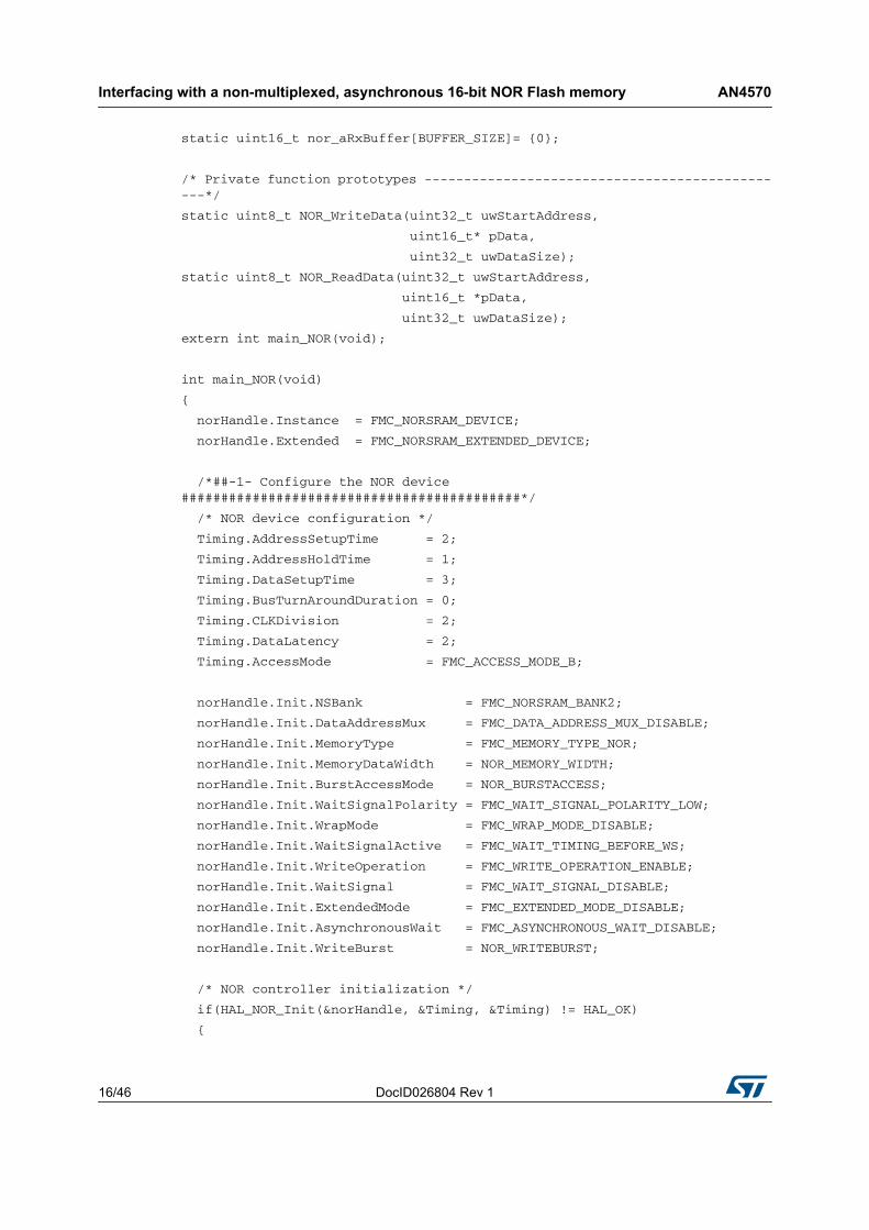
A firmware example is available hereafter.
The main goal of this example is to provide the basics of how to use the FMC firmware library and the associated NOR Flash memory driver to perform erase/read/write operations on the M29W128FL, M29W128GL or S29GL128P NOR Flash memories.
For the FMC timings, the FMC NOR Flash firmware driver uses the highest timing values, that is those of the S29GL128P NOR Flash memory.
DocID026804 Rev 1 15/46
AN4570 Interfacing with a non-multiplexed, asynchronous 16-bit NOR Flash memory
45
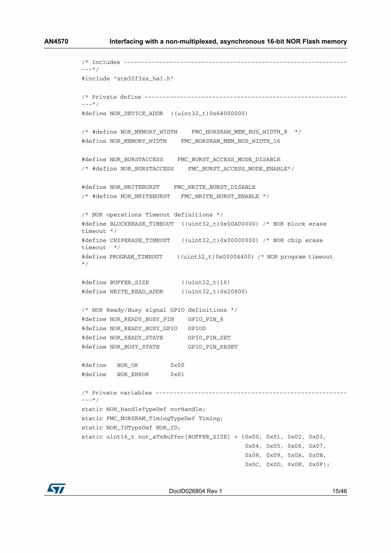
/* Includes ------------------------------------------------------------------*/
#include "stm32f3xx_hal.h"
/* Private define ------------------------------------------------------------*/
#define NOR_DEVICE_ADDR ((uint32_t)0x64000000)
/* #define NOR_MEMORY_WIDTH FMC_NORSRAM_MEM_BUS_WIDTH_8 */
#define NOR_MEMORY_WIDTH FMC_NORSRAM_MEM_BUS_WIDTH_16
#define NOR_BURSTACCESS FMC_BURST_ACCESS_MODE_DISABLE
/* #define NOR_BURSTACCESS FMC_BURST_ACCESS_MODE_ENABLE*/
#define NOR_WRITEBURST FMC_WRITE_BURST_DISABLE
/* #define NOR_WRITEBURST FMC_WRITE_BURST_ENABLE */
/* NOR operations Timeout definitions */
#define BLOCKERASE_TIMEOUT ((uint32_t)0x00A00000) /* NOR block erasetimeout */
#define CHIPERASE_TIMEOUT ((uint32_t)0x30000000) /* NOR chip erasetimeout */
#define PROGRAM_TIMEOUT ((uint32_t)0x00004400) /* NOR program timeout*/
#define BUFFER_SIZE ((uint32_t)16)
#define WRITE_READ_ADDR ((uint32_t)0x20800)
/* NOR Ready/Busy signal GPIO definitions */
#define NOR_READY_BUSY_PIN GPIO_PIN_6
#define NOR_READY_BUSY_GPIO GPIOD
#define NOR_READY_STATE GPIO_PIN_SET
#define NOR_BUSY_STATE GPIO_PIN_RESET
#define NOR_OK 0x00
#define NOR_ERROR 0x01
/* Private variables ---------------------------------------------------------*/
static NOR_HandleTypeDef norHandle;
static FMC_NORSRAM_TimingTypeDef Timing;
static NOR_IDTypeDef NOR_ID;
static uint16_t nor_aTxBuffer[BUFFER_SIZE] = {0x00, 0x01, 0x02, 0x03,
0x04, 0x05, 0x06, 0x07,
0x08, 0x09, 0x0A, 0x0B,
0x0C, 0x0D, 0x0E, 0x0F};
Interfacing with a non-multiplexed, asynchronous 16-bit NOR Flash memory AN4570
16/46 DocID026804 Rev 1
static uint16_t nor_aRxBuffer[BUFFER_SIZE]= {0};
/* Private function prototypes -----------------------------------------------*/
static uint8_t NOR_WriteData(uint32_t uwStartAddress,
uint16_t* pData,
uint32_t uwDataSize);
static uint8_t NOR_ReadData(uint32_t uwStartAddress,
uint16_t *pData,
uint32_t uwDataSize);
extern int main_NOR(void);
int main_NOR(void)
{
norHandle.Instance = FMC_NORSRAM_DEVICE;
norHandle.Extended = FMC_NORSRAM_EXTENDED_DEVICE;
/*##-1- Configure the NOR device###########################################*/
/* NOR device configuration */
Timing.AddressSetupTime = 2;
Timing.AddressHoldTime = 1;
Timing.DataSetupTime = 3;
Timing.BusTurnAroundDuration = 0;
Timing.CLKDivision = 2;
Timing.DataLatency = 2;
Timing.AccessMode = FMC_ACCESS_MODE_B;
norHandle.Init.NSBank = FMC_NORSRAM_BANK2;
norHandle.Init.DataAddressMux = FMC_DATA_ADDRESS_MUX_DISABLE;
norHandle.Init.MemoryType = FMC_MEMORY_TYPE_NOR;
norHandle.Init.MemoryDataWidth = NOR_MEMORY_WIDTH;
norHandle.Init.BurstAccessMode = NOR_BURSTACCESS;
norHandle.Init.WaitSignalPolarity = FMC_WAIT_SIGNAL_POLARITY_LOW;
norHandle.Init.WrapMode = FMC_WRAP_MODE_DISABLE;
norHandle.Init.WaitSignalActive = FMC_WAIT_TIMING_BEFORE_WS;
norHandle.Init.WriteOperation = FMC_WRITE_OPERATION_ENABLE;
norHandle.Init.WaitSignal = FMC_WAIT_SIGNAL_DISABLE;
norHandle.Init.ExtendedMode = FMC_EXTENDED_MODE_DISABLE;
norHandle.Init.AsynchronousWait = FMC_ASYNCHRONOUS_WAIT_DISABLE;
norHandle.Init.WriteBurst = NOR_WRITEBURST;
/* NOR controller initialization */
if(HAL_NOR_Init(&norHandle, &Timing, &Timing) != HAL_OK)
{
DocID026804 Rev 1 17/46
AN4570 Interfacing with a non-multiplexed, asynchronous 16-bit NOR Flash memory
45
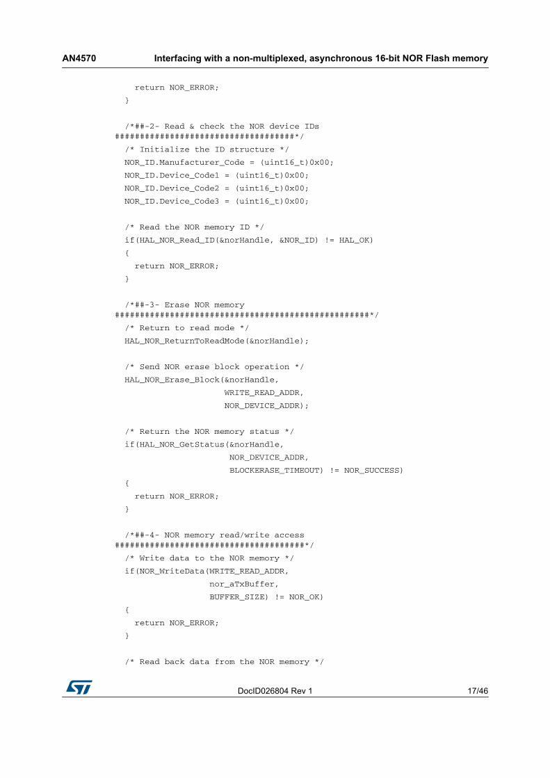
return NOR_ERROR;
}
/*##-2- Read & check the NOR device IDs####################################*/
/* Initialize the ID structure */
NOR_ID.Manufacturer_Code = (uint16_t)0x00;
NOR_ID.Device_Code1 = (uint16_t)0x00;
NOR_ID.Device_Code2 = (uint16_t)0x00;
NOR_ID.Device_Code3 = (uint16_t)0x00;
/* Read the NOR memory ID */
if(HAL_NOR_Read_ID(&norHandle, &NOR_ID) != HAL_OK)
{
return NOR_ERROR;
}
/*##-3- Erase NOR memory###################################################*/
/* Return to read mode */
HAL_NOR_ReturnToReadMode(&norHandle);
/* Send NOR erase block operation */
HAL_NOR_Erase_Block(&norHandle,
WRITE_READ_ADDR,
NOR_DEVICE_ADDR);
/* Return the NOR memory status */
if(HAL_NOR_GetStatus(&norHandle,
NOR_DEVICE_ADDR,
BLOCKERASE_TIMEOUT) != NOR_SUCCESS)
{
return NOR_ERROR;
}
/*##-4- NOR memory read/write access######################################*/
/* Write data to the NOR memory */
if(NOR_WriteData(WRITE_READ_ADDR,
nor_aTxBuffer,
BUFFER_SIZE) != NOR_OK)
{
return NOR_ERROR;
}
/* Read back data from the NOR memory */

Interfacing with a non-multiplexed, asynchronous 16-bit NOR Flash memory AN4570
18/46 DocID026804 Rev 1
if(NOR_ReadData(WRITE_READ_ADDR,
nor_aRxBuffer,
BUFFER_SIZE) != NOR_OK)
{
return NOR_ERROR;
}
return NOR_OK;
}
/**
* @brief Initializes the NOR MSP.
* @param None
* @retval None
*/
void HAL_NOR_MspInit(NOR_HandleTypeDef *hnor)
{
GPIO_InitTypeDef GPIO_Init_Structure;
/* Enable FMC clock */
__FMC_CLK_ENABLE();
/* Enable GPIOs clock */
__GPIOD_CLK_ENABLE();
__GPIOE_CLK_ENABLE();
__GPIOF_CLK_ENABLE();
__GPIOG_CLK_ENABLE();
__GPIOH_CLK_ENABLE();
/* Common GPIO configuration */
GPIO_Init_Structure.Mode = GPIO_MODE_AF_PP;
GPIO_Init_Structure.Pull = GPIO_PULLUP;
GPIO_Init_Structure.Speed = GPIO_SPEED_HIGH;
GPIO_Init_Structure.Alternate = GPIO_AF12_FMC;
/*## Data Bus #######*/
/* GPIOD configuration */
GPIO_Init_Structure.Pin = GPIO_PIN_0 | GPIO_PIN_1 | GPIO_PIN_8 |GPIO_PIN_9 |
GPIO_PIN_10 | GPIO_PIN_14 | GPIO_PIN_15;
HAL_GPIO_Init(GPIOD, &GPIO_Init_Structure);
/* GPIOE configuration */
DocID026804 Rev 1 19/46
AN4570 Interfacing with a non-multiplexed, asynchronous 16-bit NOR Flash memory
45
GPIO_Init_Structure.Pin = GPIO_PIN_7 | GPIO_PIN_8 | GPIO_PIN_9 |GPIO_PIN_10 |
GPIO_PIN_11 | GPIO_PIN_12 | GPIO_PIN_13 |
GPIO_PIN_14 | GPIO_PIN_15;
HAL_GPIO_Init(GPIOE, &GPIO_Init_Structure);
/*## Address Bus #######*/
/* GPIOF configuration */
GPIO_Init_Structure.Pin = GPIO_PIN_2 | GPIO_PIN_3 |
GPIO_PIN_4 | GPIO_PIN_5 | GPIO_PIN_12 |GPIO_PIN_13 |
GPIO_PIN_14 | GPIO_PIN_15;
HAL_GPIO_Init(GPIOF, &GPIO_Init_Structure);
GPIO_Init_Structure.Pin = GPIO_PIN_0 | GPIO_PIN_1;
HAL_GPIO_Init(GPIOH, &GPIO_Init_Structure);
/* GPIOG configuration */
GPIO_Init_Structure.Pin = GPIO_PIN_0 | GPIO_PIN_1 | GPIO_PIN_2 |
GPIO_PIN_3 | GPIO_PIN_4 | GPIO_PIN_5;
HAL_GPIO_Init(GPIOG, &GPIO_Init_Structure);
/* GPIOD configuration */
GPIO_Init_Structure.Pin = GPIO_PIN_11 | GPIO_PIN_12 | GPIO_PIN_13;
HAL_GPIO_Init(GPIOD, &GPIO_Init_Structure);
/* GPIOE configuration */
GPIO_Init_Structure.Pin = GPIO_PIN_3 | GPIO_PIN_4 | GPIO_PIN_5 |GPIO_PIN_6;
HAL_GPIO_Init(GPIOE, &GPIO_Init_Structure);
/*## NOE and NWE configuration ######*/
GPIO_Init_Structure.Pin = GPIO_PIN_4 | GPIO_PIN_5;
HAL_GPIO_Init(GPIOD, &GPIO_Init_Structure);
/*## NE2 configuration ######*/
GPIO_Init_Structure.Pin = GPIO_PIN_9;
HAL_GPIO_Init(GPIOG, &GPIO_Init_Structure);
/*## Configure PD6 for NOR memory Ready/Busy signal ######*/
GPIO_Init_Structure.Pin = GPIO_PIN_6;
GPIO_Init_Structure.Mode = GPIO_MODE_AF_PP;
GPIO_Init_Structure.Pull = GPIO_PULLUP;
GPIO_Init_Structure.Alternate = GPIO_AF12_FMC;
HAL_GPIO_Init(GPIOD, &GPIO_Init_Structure);
}
Interfacing with a non-multiplexed, asynchronous 16-bit NOR Flash memory AN4570
20/46 DocID026804 Rev 1
/**
* @brief NOR BSP Wait for Ready/Busy signal.
* @param hnor: Pointer to NOR handle
* @param Timeout: Timeout duration
* @retval None
*/
void HAL_NOR_MspWait(NOR_HandleTypeDef *hnor,
uint32_t Timeout)
{
uint32_t timeout = Timeout;
/* Polling on Ready/Busy signal */
while((HAL_GPIO_ReadPin(NOR_READY_BUSY_GPIO,
NOR_READY_BUSY_PIN) != NOR_BUSY_STATE) && (timeout> 0))
{
timeout--;
}
timeout = Timeout;
/* Polling on Ready/Busy signal */
while((HAL_GPIO_ReadPin(NOR_READY_BUSY_GPIO,
NOR_READY_BUSY_PIN) != NOR_READY_STATE) && (timeout> 0))
{
timeout--;
}
}
/**
* @brief Writes an amount of data to the NOR device.
* @param uwStartAddress: Write start address
* @param pData: Pointer to data to be written
* @param uwDataSize: Size of data to write
* @retval NOR memory status
*/
uint8_t NOR_WriteData(uint32_t uwStartAddress,
uint16_t* pData,
uint32_t uwDataSize)
{
uint32_t index = uwDataSize;
while(index > 0)
DocID026804 Rev 1 21/46
AN4570 Interfacing with a non-multiplexed, asynchronous 16-bit NOR Flash memory
45
{
/* Write data to NOR */
HAL_NOR_Program(&norHandle,
(uint32_t *)(NOR_DEVICE_ADDR + uwStartAddress),
pData);
/* Read NOR device status */
if(HAL_NOR_GetStatus(&norHandle,
NOR_DEVICE_ADDR,
PROGRAM_TIMEOUT) != NOR_SUCCESS)
{
return NOR_ERROR;
}
/* Update the counters */
index--;
uwStartAddress += 2;
pData++;
}
return NOR_OK;
}
/**
* @brief Reads an amount of data from the NOR device.
* @param uwStartAddress: Read start address
* @param pData: Pointer to data to be read
* @param uwDataSize: Size of data to read
* @retval NOR memory status
*/
uint8_t NOR_ReadData(uint32_t uwStartAddress,
uint16_t* pData,
uint32_t uwDataSize)
{
if(HAL_NOR_ReadBuffer(&norHandle,
NOR_DEVICE_ADDR + uwStartAddress,
pData, uwDataSize) != HAL_OK)
{
return NOR_ERROR;
}
else
{
return NOR_OK;
}
}
Interfacing with a non-multiplexed, asynchronous 16-bit SRAM AN4570
22/46 DocID026804 Rev 1
3 Interfacing with a non-multiplexed, asynchronous 16-bit SRAM
3.1 FMC configurationSRAM and NOR Flash memories share the same FMC banks. The protocol to be used depends on the selected memory type.
To control an SRAM, the FMC provides the following possible features:• Enable or disable the address/data multiplexing feature• Select the memory type to be used: NOR/SRAM/PSRAM• Define the external memory data bus width: 8/16 bits• Enable or disable the extended mode: this mode is used to access the memory with a
different timing configuration for read and write operations.
Like for NOR Flash memories, the user has to compute and set the following parameters as a function of the information in the SRAM datasheet:
ADDSET: address setup timeDATAST: data setup time
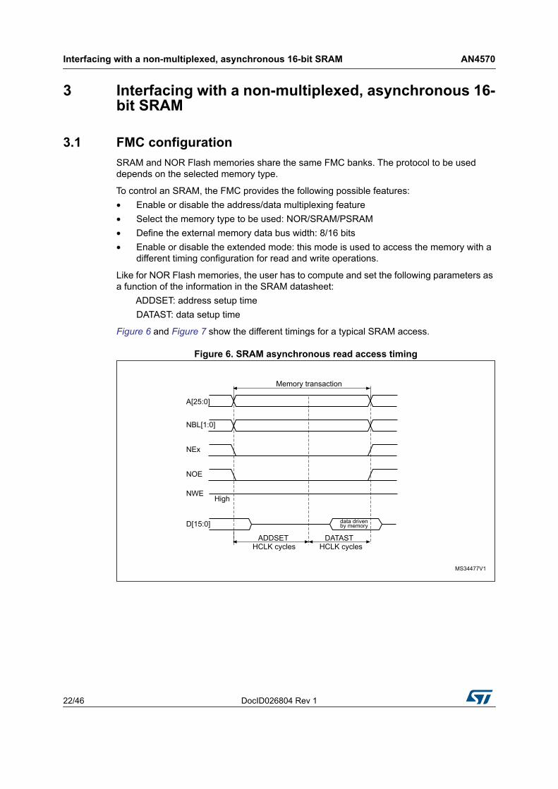
Figure 6 and Figure 7 show the different timings for a typical SRAM access.
Figure 6. SRAM asynchronous read access timing
DocID026804 Rev 1 23/46
AN4570 Interfacing with a non-multiplexed, asynchronous 16-bit SRAM
45
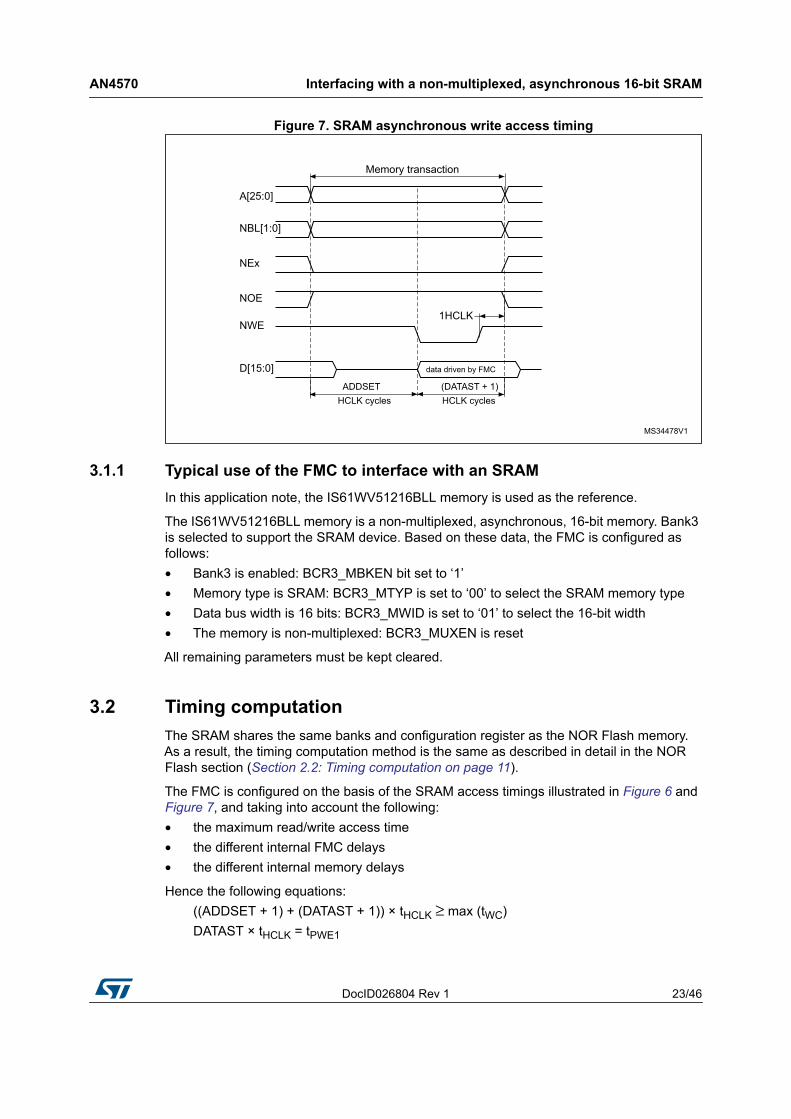
Figure 7. SRAM asynchronous write access timing
3.1.1 Typical use of the FMC to interface with an SRAMIn this application note, the IS61WV51216BLL memory is used as the reference.
The IS61WV51216BLL memory is a non-multiplexed, asynchronous, 16-bit memory. Bank3 is selected to support the SRAM device. Based on these data, the FMC is configured as follows:• Bank3 is enabled: BCR3_MBKEN bit set to ‘1’• Memory type is SRAM: BCR3_MTYP is set to ‘00’ to select the SRAM memory type• Data bus width is 16 bits: BCR3_MWID is set to ‘01’ to select the 16-bit width• The memory is non-multiplexed: BCR3_MUXEN is reset
All remaining parameters must be kept cleared.
3.2 Timing computationThe SRAM shares the same banks and configuration register as the NOR Flash memory. As a result, the timing computation method is the same as described in detail in the NOR Flash section (Section 2.2: Timing computation on page 11).
The FMC is configured on the basis of the SRAM access timings illustrated in Figure 6 and Figure 7, and taking into account the following:• the maximum read/write access time• the different internal FMC delays• the different internal memory delays
Hence the following equations:((ADDSET + 1) + (DATAST + 1)) × tHCLK ≥ max (tWC)DATAST × tHCLK = tPWE1

Interfacing with a non-multiplexed, asynchronous 16-bit SRAM AN4570
24/46 DocID026804 Rev 1
For read access, DATAST must verify:DATAST ≥ (tAA + tsu(Data_NE) + tv(A_NE))/tHCLK – ADDSET – 4
Table 6 gives the meanings and values of the SRAM parameters.
Using the above described formulas, the memory timings in Table 6 and the asynchronous timings in Table 3, we have:• Address setup time: 0x0• Data setup time: 0x1
3.3 Hardware connectionTable 7 gives the correspondence between SRAM pins and FMC pins and shows the GPIO configuration for each FMC pin.
In case of an 8-bit SRAM, the data/address bus is 8 bits wide and D8-D15 should not be connected to the FMC. The unused FMC pins can be used as general purpose I/O pins
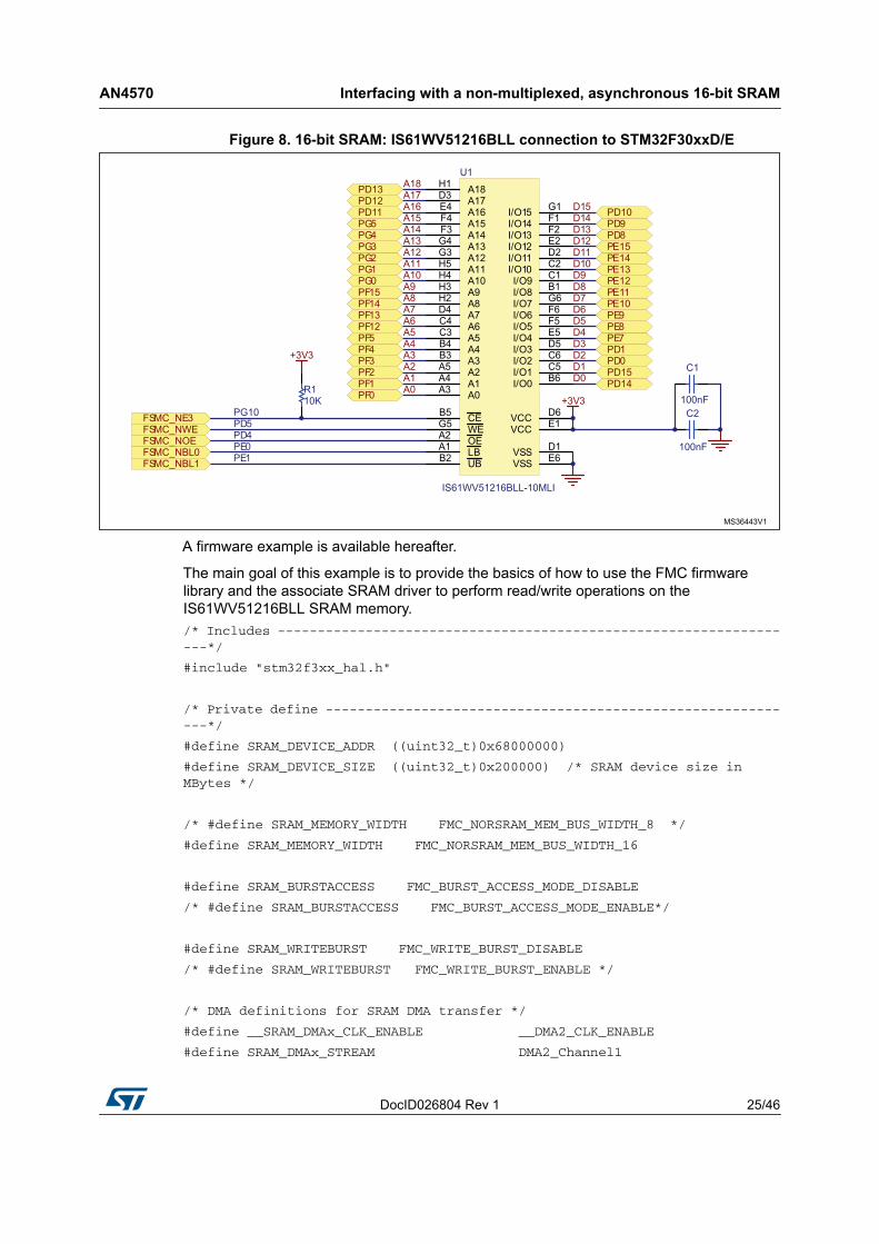
Figure 8 shows a typical connection between an STM32F30xxD/E microcontroller and an IS61WV51216BLL SRAM.
Table 6. IS61WV51216BL SRAM timings Symbols Parameter Value Unit
tWC Write cycle time 12 ns
tRC Read cycle time 12 ns
tPWE1 Write Enable low pulse width 8 ns
tAA Address access time 12 ns
Table 7. IS61WV51216BLL signal to FMC pin correspondence Memory signals FMC signals Pin / Port assignment Pin / Port
configuration Signal description
A0-A18 A0-A18 Port F/Port G/Port E/ Port D/Port H AF push-pull Address A0-A18
I/O0-I/O15 D0-D15 Port D/Port E AF push-pull Data D0-D15
CE NE3 PG10 AF push-pull Chip Enable
OE NOE PD4 AF push-pull Output Enable
WE NWE PD5 AF push-pull Write Enable
LB NBL0 PE0 AF push-pull Lower byte control
UB NBL1 PE1 AF push-pull Upper byte control
DocID026804 Rev 1 25/46
AN4570 Interfacing with a non-multiplexed, asynchronous 16-bit SRAM
45
Figure 8. 16-bit SRAM: IS61WV51216BLL connection to STM32F30xxD/E
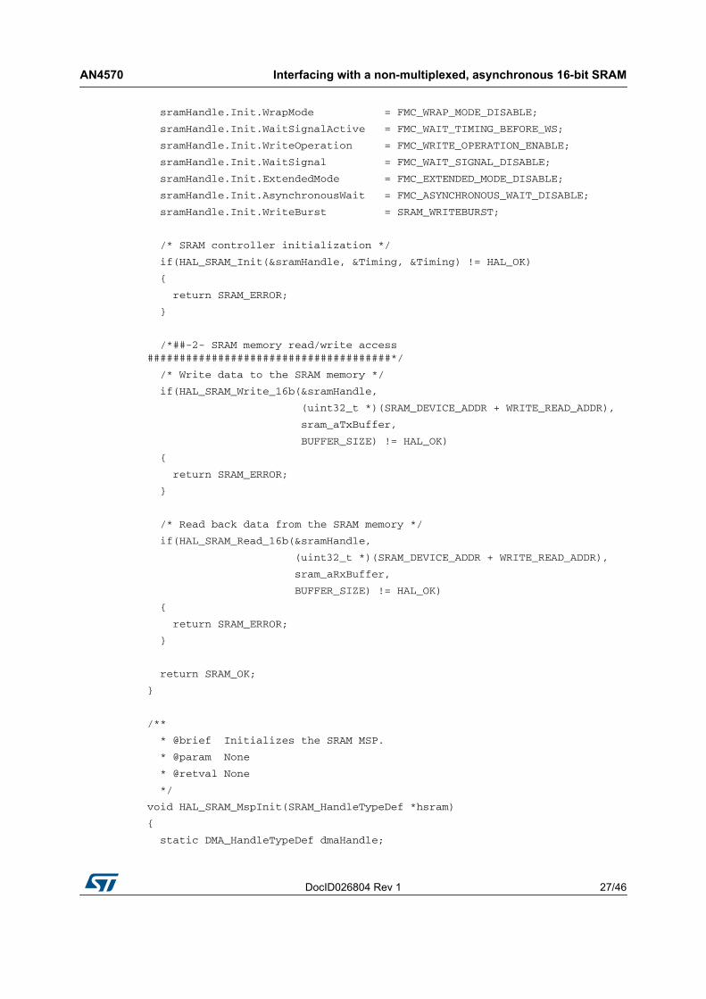
A firmware example is available hereafter.
The main goal of this example is to provide the basics of how to use the FMC firmware library and the associate SRAM driver to perform read/write operations on the IS61WV51216BLL SRAM memory./* Includes ------------------------------------------------------------------*/
#include "stm32f3xx_hal.h"
/* Private define ------------------------------------------------------------*/
#define SRAM_DEVICE_ADDR ((uint32_t)0x68000000)
#define SRAM_DEVICE_SIZE ((uint32_t)0x200000) /* SRAM device size inMBytes */
/* #define SRAM_MEMORY_WIDTH FMC_NORSRAM_MEM_BUS_WIDTH_8 */
#define SRAM_MEMORY_WIDTH FMC_NORSRAM_MEM_BUS_WIDTH_16
#define SRAM_BURSTACCESS FMC_BURST_ACCESS_MODE_DISABLE
/* #define SRAM_BURSTACCESS FMC_BURST_ACCESS_MODE_ENABLE*/
#define SRAM_WRITEBURST FMC_WRITE_BURST_DISABLE
/* #define SRAM_WRITEBURST FMC_WRITE_BURST_ENABLE */
/* DMA definitions for SRAM DMA transfer */
#define __SRAM_DMAx_CLK_ENABLE __DMA2_CLK_ENABLE
#define SRAM_DMAx_STREAM DMA2_Channel1

Interfacing with a non-multiplexed, asynchronous 16-bit SRAM AN4570
26/46 DocID026804 Rev 1
#define SRAM_DMAx_IRQn DMA2_Channel1_IRQn
#define SRAM_DMAx_IRQHandler DMA2_Channel1_IRQHandler
#define BUFFER_SIZE ((uint32_t)16)
#define WRITE_READ_ADDR ((uint32_t)0x0800)
#define SRAM_OK 0x00
#define SRAM_ERROR 0x01
/* Private variables ---------------------------------------------------------*/
SRAM_HandleTypeDef sramHandle;
static FMC_NORSRAM_TimingTypeDef Timing;
static uint16_t sram_aTxBuffer[BUFFER_SIZE] = {0x00, 0x01, 0x02, 0x03,
0x04, 0x05, 0x06, 0x07,
0x08, 0x09, 0x0A, 0x0B,
0x0C, 0x0D, 0x0E, 0x0F};
static uint16_t sram_aRxBuffer[BUFFER_SIZE]= {0};
/* Private function prototypes -----------------------------------------------*/
extern int main_SRAM(void);
int main_SRAM(void)
{
sramHandle.Instance = FMC_NORSRAM_DEVICE;
sramHandle.Extended = FMC_NORSRAM_EXTENDED_DEVICE;
/*##-1- Configure the SRAM device##########################################*/
/* SRAM device configuration */
Timing.AddressSetupTime = 0;
Timing.AddressHoldTime = 1;
Timing.DataSetupTime = 2;
Timing.BusTurnAroundDuration = 1;
Timing.CLKDivision = 2;
Timing.DataLatency = 2;
Timing.AccessMode = FMC_ACCESS_MODE_A;
sramHandle.Init.NSBank = FMC_NORSRAM_BANK3;
sramHandle.Init.DataAddressMux = FMC_DATA_ADDRESS_MUX_DISABLE;
sramHandle.Init.MemoryType = FMC_MEMORY_TYPE_SRAM;
sramHandle.Init.MemoryDataWidth = SRAM_MEMORY_WIDTH;
sramHandle.Init.BurstAccessMode = SRAM_BURSTACCESS;
sramHandle.Init.WaitSignalPolarity = FMC_WAIT_SIGNAL_POLARITY_LOW;
DocID026804 Rev 1 27/46
AN4570 Interfacing with a non-multiplexed, asynchronous 16-bit SRAM
45
sramHandle.Init.WrapMode = FMC_WRAP_MODE_DISABLE;
sramHandle.Init.WaitSignalActive = FMC_WAIT_TIMING_BEFORE_WS;
sramHandle.Init.WriteOperation = FMC_WRITE_OPERATION_ENABLE;
sramHandle.Init.WaitSignal = FMC_WAIT_SIGNAL_DISABLE;
sramHandle.Init.ExtendedMode = FMC_EXTENDED_MODE_DISABLE;
sramHandle.Init.AsynchronousWait = FMC_ASYNCHRONOUS_WAIT_DISABLE;
sramHandle.Init.WriteBurst = SRAM_WRITEBURST;
/* SRAM controller initialization */
if(HAL_SRAM_Init(&sramHandle, &Timing, &Timing) != HAL_OK)
{
return SRAM_ERROR;
}
/*##-2- SRAM memory read/write access######################################*/
/* Write data to the SRAM memory */
if(HAL_SRAM_Write_16b(&sramHandle,
(uint32_t *)(SRAM_DEVICE_ADDR + WRITE_READ_ADDR),
sram_aTxBuffer,
BUFFER_SIZE) != HAL_OK)
{
return SRAM_ERROR;
}
/* Read back data from the SRAM memory */
if(HAL_SRAM_Read_16b(&sramHandle,
(uint32_t *)(SRAM_DEVICE_ADDR + WRITE_READ_ADDR),
sram_aRxBuffer,
BUFFER_SIZE) != HAL_OK)
{
return SRAM_ERROR;
}
return SRAM_OK;
}
/**
* @brief Initializes the SRAM MSP.
* @param None
* @retval None
*/
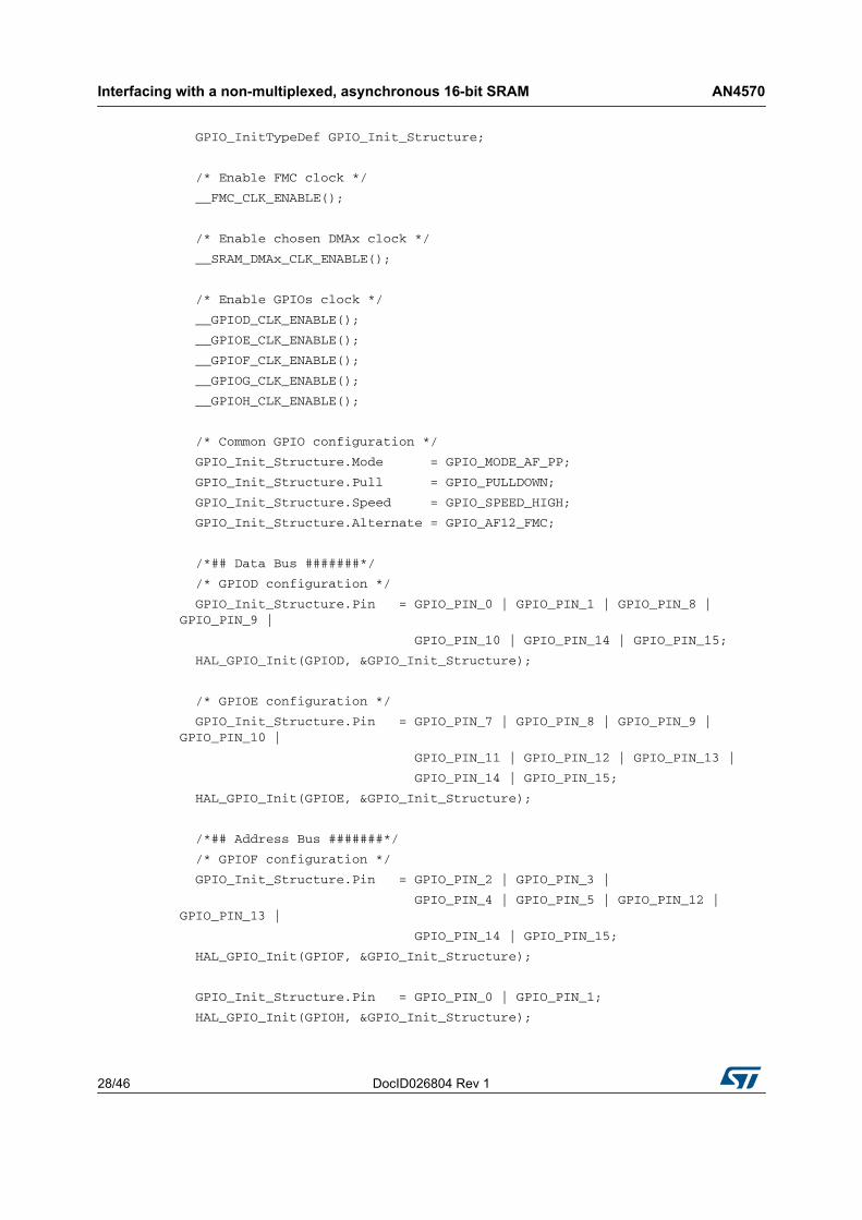
void HAL_SRAM_MspInit(SRAM_HandleTypeDef *hsram)
{
static DMA_HandleTypeDef dmaHandle;
Interfacing with a non-multiplexed, asynchronous 16-bit SRAM AN4570
28/46 DocID026804 Rev 1
GPIO_InitTypeDef GPIO_Init_Structure;
/* Enable FMC clock */
__FMC_CLK_ENABLE();
/* Enable chosen DMAx clock */
__SRAM_DMAx_CLK_ENABLE();
/* Enable GPIOs clock */
__GPIOD_CLK_ENABLE();
__GPIOE_CLK_ENABLE();
__GPIOF_CLK_ENABLE();
__GPIOG_CLK_ENABLE();
__GPIOH_CLK_ENABLE();
/* Common GPIO configuration */
GPIO_Init_Structure.Mode = GPIO_MODE_AF_PP;
GPIO_Init_Structure.Pull = GPIO_PULLDOWN;
GPIO_Init_Structure.Speed = GPIO_SPEED_HIGH;
GPIO_Init_Structure.Alternate = GPIO_AF12_FMC;
/*## Data Bus #######*/
/* GPIOD configuration */
GPIO_Init_Structure.Pin = GPIO_PIN_0 | GPIO_PIN_1 | GPIO_PIN_8 |GPIO_PIN_9 |
GPIO_PIN_10 | GPIO_PIN_14 | GPIO_PIN_15;
HAL_GPIO_Init(GPIOD, &GPIO_Init_Structure);
/* GPIOE configuration */
GPIO_Init_Structure.Pin = GPIO_PIN_7 | GPIO_PIN_8 | GPIO_PIN_9 |GPIO_PIN_10 |
GPIO_PIN_11 | GPIO_PIN_12 | GPIO_PIN_13 |
GPIO_PIN_14 | GPIO_PIN_15;
HAL_GPIO_Init(GPIOE, &GPIO_Init_Structure);
/*## Address Bus #######*/
/* GPIOF configuration */
GPIO_Init_Structure.Pin = GPIO_PIN_2 | GPIO_PIN_3 |
GPIO_PIN_4 | GPIO_PIN_5 | GPIO_PIN_12 |GPIO_PIN_13 |
GPIO_PIN_14 | GPIO_PIN_15;
HAL_GPIO_Init(GPIOF, &GPIO_Init_Structure);
GPIO_Init_Structure.Pin = GPIO_PIN_0 | GPIO_PIN_1;
HAL_GPIO_Init(GPIOH, &GPIO_Init_Structure);
DocID026804 Rev 1 29/46
AN4570 Interfacing with a non-multiplexed, asynchronous 16-bit SRAM
45
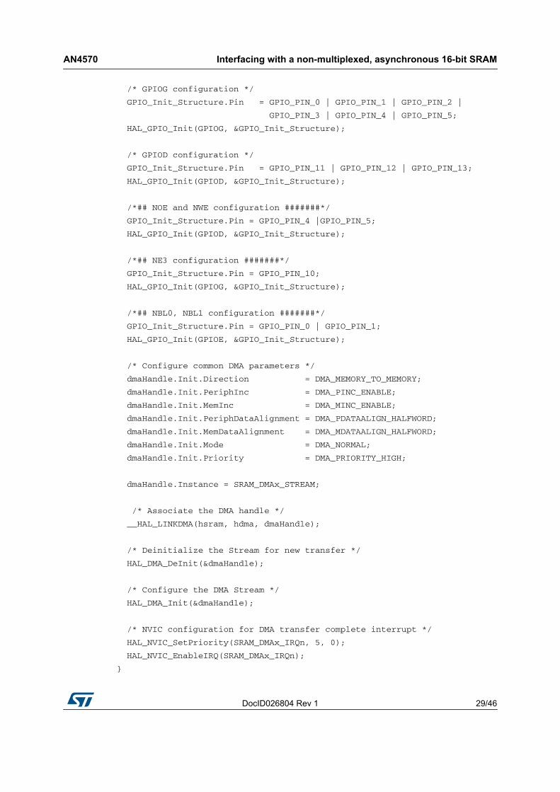
/* GPIOG configuration */
GPIO_Init_Structure.Pin = GPIO_PIN_0 | GPIO_PIN_1 | GPIO_PIN_2 |
GPIO_PIN_3 | GPIO_PIN_4 | GPIO_PIN_5;
HAL_GPIO_Init(GPIOG, &GPIO_Init_Structure);
/* GPIOD configuration */
GPIO_Init_Structure.Pin = GPIO_PIN_11 | GPIO_PIN_12 | GPIO_PIN_13;
HAL_GPIO_Init(GPIOD, &GPIO_Init_Structure);
/*## NOE and NWE configuration #######*/
GPIO_Init_Structure.Pin = GPIO_PIN_4 |GPIO_PIN_5;
HAL_GPIO_Init(GPIOD, &GPIO_Init_Structure);
/*## NE3 configuration #######*/
GPIO_Init_Structure.Pin = GPIO_PIN_10;
HAL_GPIO_Init(GPIOG, &GPIO_Init_Structure);
/*## NBL0, NBL1 configuration #######*/
GPIO_Init_Structure.Pin = GPIO_PIN_0 | GPIO_PIN_1;
HAL_GPIO_Init(GPIOE, &GPIO_Init_Structure);
/* Configure common DMA parameters */
dmaHandle.Init.Direction = DMA_MEMORY_TO_MEMORY;
dmaHandle.Init.PeriphInc = DMA_PINC_ENABLE;
dmaHandle.Init.MemInc = DMA_MINC_ENABLE;
dmaHandle.Init.PeriphDataAlignment = DMA_PDATAALIGN_HALFWORD;
dmaHandle.Init.MemDataAlignment = DMA_MDATAALIGN_HALFWORD;
dmaHandle.Init.Mode = DMA_NORMAL;
dmaHandle.Init.Priority = DMA_PRIORITY_HIGH;
dmaHandle.Instance = SRAM_DMAx_STREAM;
/* Associate the DMA handle */
__HAL_LINKDMA(hsram, hdma, dmaHandle);
/* Deinitialize the Stream for new transfer */
HAL_DMA_DeInit(&dmaHandle);
/* Configure the DMA Stream */
HAL_DMA_Init(&dmaHandle);
/* NVIC configuration for DMA transfer complete interrupt */
HAL_NVIC_SetPriority(SRAM_DMAx_IRQn, 5, 0);
HAL_NVIC_EnableIRQ(SRAM_DMAx_IRQn);
}
Interfacing with an 8-bit NAND Flash memory AN4570
30/46 DocID026804 Rev 1
4 Interfacing with an 8-bit NAND Flash memory
NAND Flash memories are accessed in accordance with a specific protocol. To write to or read from the NAND Flash memory, it is necessary to:1. Send a command to the NAND Flash memory2. Send the address to write to or read from3. Read or write the data
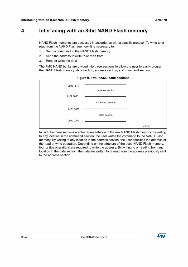
The FMC NAND banks are divided into three sections to allow the user to easily program the NAND Flash memory: data section, address section, and command section.
Figure 9. FMC NAND bank sections
In fact, the three sections are the representation of the real NAND Flash memory. By writing to any location in the command section, the user writes the command to the NAND Flash memory. By writing to any location in the address section, the user specifies the address of the read or write operation. Depending on the structure of the used NAND Flash memory, four or five operations are required to write the address. By writing to or reading from any location in the data section, the data are written to or read from the address previously sent to the address section.
Command section
Address section
Data section
0x02 0000
0x03 FFFF
0x01 0000
0x00 0000
ai15182
DocID026804 Rev 1 31/46
AN4570 Interfacing with an 8-bit NAND Flash memory
45
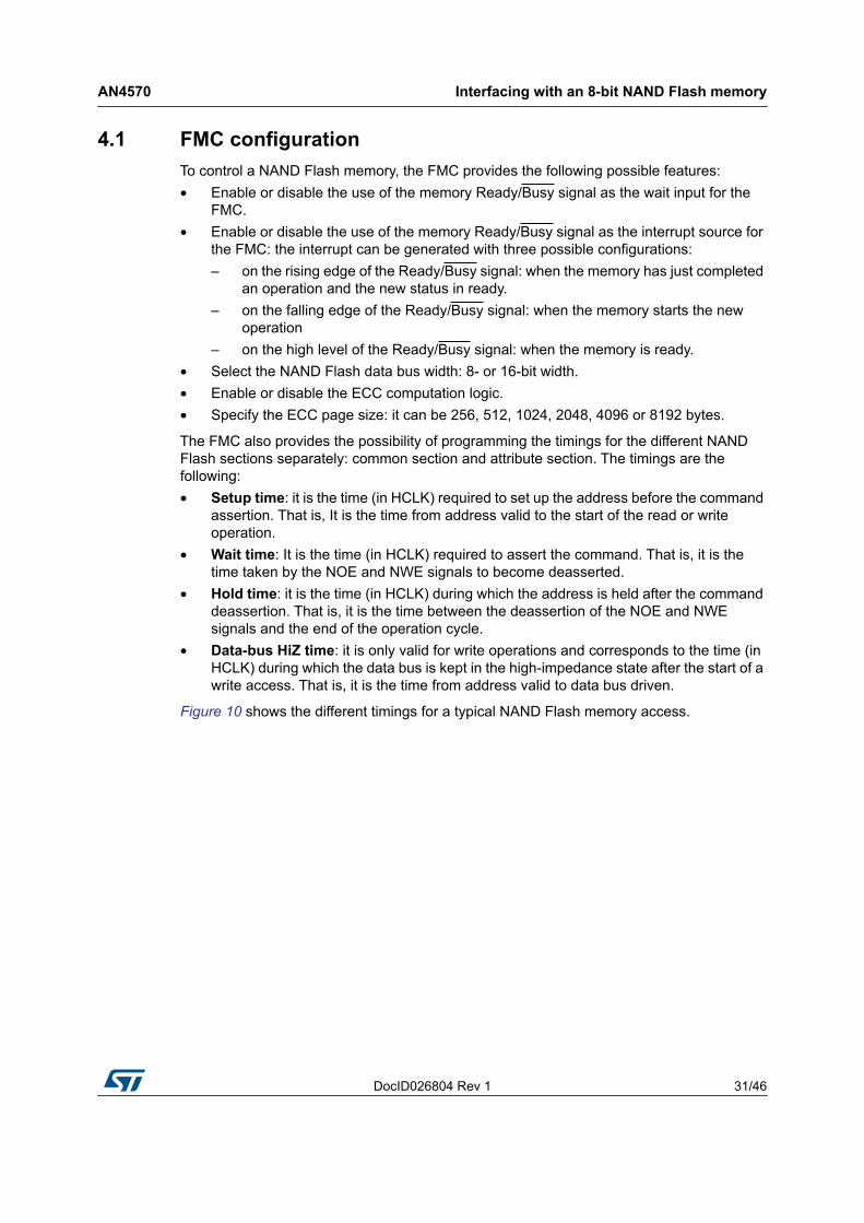
4.1 FMC configurationTo control a NAND Flash memory, the FMC provides the following possible features:• Enable or disable the use of the memory Ready/Busy signal as the wait input for the
FMC.• Enable or disable the use of the memory Ready/Busy signal as the interrupt source for
the FMC: the interrupt can be generated with three possible configurations:– on the rising edge of the Ready/Busy signal: when the memory has just completed
an operation and the new status in ready.– on the falling edge of the Ready/Busy signal: when the memory starts the new
operation– on the high level of the Ready/Busy signal: when the memory is ready.
• Select the NAND Flash data bus width: 8- or 16-bit width.• Enable or disable the ECC computation logic.• Specify the ECC page size: it can be 256, 512, 1024, 2048, 4096 or 8192 bytes.
The FMC also provides the possibility of programming the timings for the different NAND Flash sections separately: common section and attribute section. The timings are the following:• Setup time: it is the time (in HCLK) required to set up the address before the command
assertion. That is, It is the time from address valid to the start of the read or write operation.
• Wait time: It is the time (in HCLK) required to assert the command. That is, it is the time taken by the NOE and NWE signals to become deasserted.
• Hold time: it is the time (in HCLK) during which the address is held after the command deassertion. That is, it is the time between the deassertion of the NOE and NWE signals and the end of the operation cycle.
• Data-bus HiZ time: it is only valid for write operations and corresponds to the time (in HCLK) during which the data bus is kept in the high-impedance state after the start of a write access. That is, it is the time from address valid to data bus driven.
Figure 10 shows the different timings for a typical NAND Flash memory access.
Interfacing with an 8-bit NAND Flash memory AN4570
32/46 DocID026804 Rev 1
Figure 10. NAND memory access timing
1. NOE remains high (inactive) during write accesses. NWE remains high (inactive) during read accesses.
4.1.1 Typical use of the FMC to interface with a NAND memoryThe STM32F30xxD/E FMC NAND Flash controller can configure Bank2 or Bank3 to support NAND Flash memories.
The banks are selected using the Chip Select signals, as each bank is associated with a specific Chip Select.
To enable communication with the NAND Flash devices, the FMC NAND Flash controller has to be initialized to meet the characteristics of the NAND Flash devices: features, timings, data width, etc.
In this application note, the Numonyx NAND512W3A is used as the reference. This memory has the same access protocol as many other NAND Flash memories on today’s market.
NAND512W3A characteristics:• NAND interface: x8 bus width, multiplexed address/ data• Page size: x8 device: (512 + 16 spare) bytes• Page Read/Program timings:
– Random access: 12 μs (3 V)/15 μs (1.8 V) (max)– Sequential access: 30 ns (3 V)/50 ns (1.8 V) (min)– Page Program time: 200 μs (typ.)
DocID026804 Rev 1 33/46
AN4570 Interfacing with an 8-bit NAND Flash memory
45
Bank2 is selected to support the NAND Flash device. Based on these data, the FMC is configured as follows:• Bank2 is enabled: PCR2_PBKEN bit set to ‘1’• Memory type is NAND Flash: PCR2_PTYP is set to ‘1’ to select the NAND Flash
memory type.• Data bus width is 8 bit: PCR2_PWID is set to ‘00’ to select 8-bit width.• ECC page size is 512 bytes: PCR2_ECCPS is set to ‘001’ to set the ECC computation
page size to 512 bytes.• ECC hardware calculation on/off as needed: PCR2_ECCEN is set or reset accordingly.• Wait feature may or not be enabled depending on the user’s application:
PCR2_PWAITEN is set or reset as needed.
The Ready/Busy memory signal can be connected to the FSMC_NWAIT pin, and in this case the Wait feature must be used to manage the NAND Flash operations.
When using the NAND Flash memory with the wait feature enabled, the controller waits for the NAND Flash to be ready to become active before starting a new access. While waiting, the controller maintains the NCE signal active (low).
Generally, the Ready/Busy signal is an open-drain output. To connect this signal to the STM32F30xxD/E microcontroller, the corresponding pin must be configured as input pull-up.
The Ready/Busy signal can be used as an interrupt source for the FMC and, in this case, the CPU can perform other tasks during NAND Flash operations. Three FMC configurations make it possible to use this signal as an interrupt. For that purpose, the IREN, IFEN or ILEN bits in the SR2 register are used to select the rising edge, the falling edge or the high level of the NAND Flash Ready/Busy signal.
4.2 Timing computationBesides configuring the different features that are to be used with the NAND Flash memory, the user has to initialize the controller to meet the memory timings.
As described in Section 4.1, the FMC is able to program four different timings for the common space and the attribute space independently: Setup time, Wait time, Hold time and Data-bus HiZ time.
These parameters are computed according to the NAND Flash memory characteristics and the STM32F30xxD/E HCLK clock.
Interfacing with an 8-bit NAND Flash memory AN4570
34/46 DocID026804 Rev 1
Based on the NAND Flash memory access timings shown in Figure 10, the following equations are found:• The write or read access time is the time between the falling edge and the rising edge
of the NAND Flash memory Chip Select signal. It is computed as a function of the FMC timing parameter:
((SET + 1) + (WAIT + 1) + (HOLD + 1)) × tHCLK ≥ Write/Read access • The Wait time is measured between the falling edge and the rising edge of the
Write/Read Enable signal:Write/Read Enable signal low to high = (WAIT + 1) × tHCLK
• For write access, the HIZ parameter is the time measured between the falling edge of the Chip Select signal and the data setup on bus:
(HIZ+1) x tHCLK ≥ Chip Select setup time to Data setup.• The HOLD timing is given in the NAND datasheet as follows:
(HOLD +1) x tHCLK = Write Enable High to Chip Enable / Address/Command Latch High
To make sure of the correct timing configuration of the FMC, the timings have to take into consideration:• The maximum read/write access time• The different internal FMC delays• The different internal memory delays
Hence, we have the following equations following the NAND512W3A NAND datasheet:• (SET + 1) x tHCLK ≥ max (tCS, tCLS, tALS, tCLR, tAR) - tWP • (WAIT + 1) x tHCLK ≥ max (tWP, tRP) • (HIZ + 1) x tHCLK ≥ max (tCS, tALS, tCLS) + (tWP - tDS)• (HOLD + 1) x tHCLK ≥ max (tCH, tCLH, tALH)• ((WAIT + 1) + (HOLD + 1) + (SET + 1)) x tHCLK ≥ max (tWC/RC)
Considering the different timings in the FMC and the memory, the equations become:• WAIT must verify:
(WAIT + 1)× tHCLK ≥ (tREA + tsu(D-NOE))
WAIT ≥ (tREA + tsu(D-NOE)) /tHCLK - 1
Note: tsu(D-NOE) is specified in the STM32F30xxD/E datasheets. tsu(D-NOE) = 25 ns
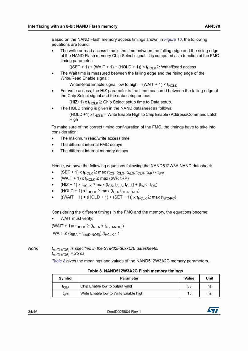
Table 8 gives the meanings and values of the NAND512W3A2C memory parameters.
Table 8. NAND512W3A2C Flash memory timings Symbol Parameter Value Unit
tCEA Chip Enable low to output valid 35 ns
tWP Write Enable low to Write Enable high 15 ns
DocID026804 Rev 1 35/46
AN4570 Interfacing with an 8-bit NAND Flash memory
45
Using the above described formulas, the memory timings in Table 8 and the asynchronous timings in Table 3, we have:• Setup time: 0x0• Wait time: 0x2• Hold time: 0x1• HiZ time: 0x0
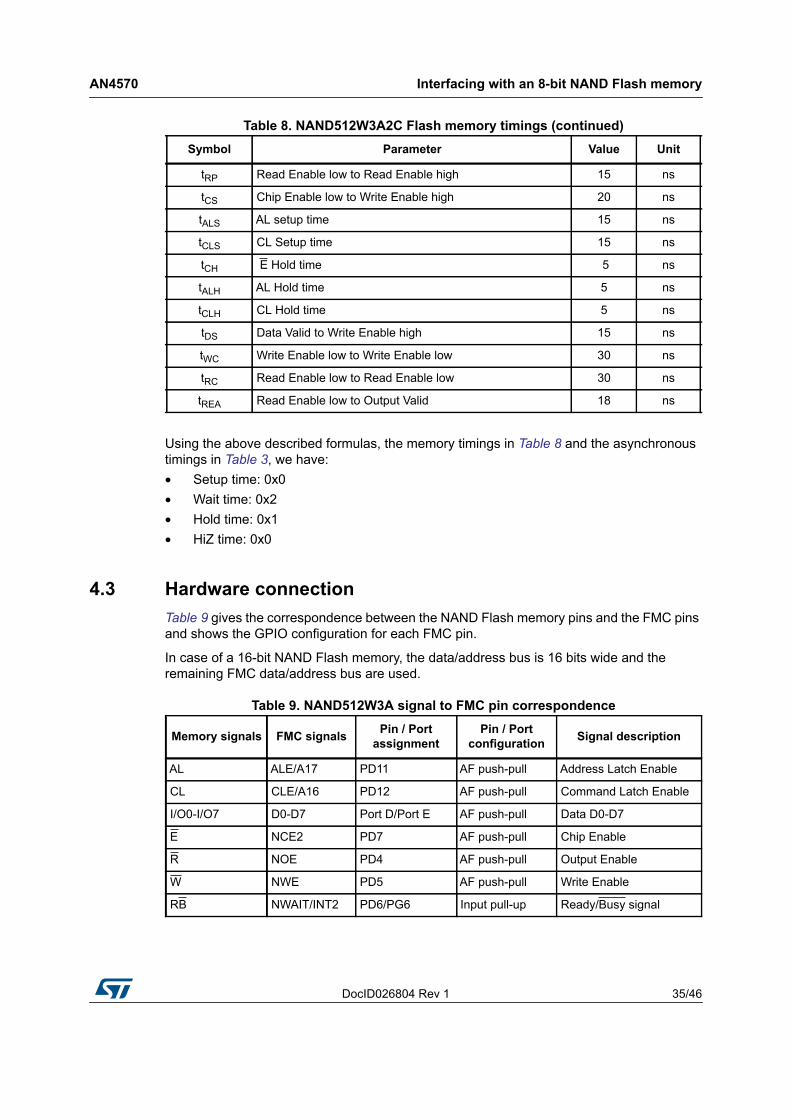
4.3 Hardware connectionTable 9 gives the correspondence between the NAND Flash memory pins and the FMC pins and shows the GPIO configuration for each FMC pin.
In case of a 16-bit NAND Flash memory, the data/address bus is 16 bits wide and the remaining FMC data/address bus are used.
tRP Read Enable low to Read Enable high 15 ns
tCS Chip Enable low to Write Enable high 20 ns
tALS AL setup time 15 ns
tCLS CL Setup time 15 ns
tCH E Hold time 5 ns
tALH AL Hold time 5 ns
tCLH CL Hold time 5 ns
tDS Data Valid to Write Enable high 15 ns
tWC Write Enable low to Write Enable low 30 ns
tRC Read Enable low to Read Enable low 30 ns
tREA Read Enable low to Output Valid 18 ns
Table 8. NAND512W3A2C Flash memory timings (continued)Symbol Parameter Value Unit
Table 9. NAND512W3A signal to FMC pin correspondence
Memory signals FMC signals Pin / Port assignment
Pin / Port configuration Signal description
AL ALE/A17 PD11 AF push-pull Address Latch Enable
CL CLE/A16 PD12 AF push-pull Command Latch Enable
I/O0-I/O7 D0-D7 Port D/Port E AF push-pull Data D0-D7
E NCE2 PD7 AF push-pull Chip Enable
R NOE PD4 AF push-pull Output Enable
W NWE PD5 AF push-pull Write Enable
RB NWAIT/INT2 PD6/PG6 Input pull-up Ready/Busy signal
Interfacing with an 8-bit NAND Flash memory AN4570
36/46 DocID026804 Rev 1
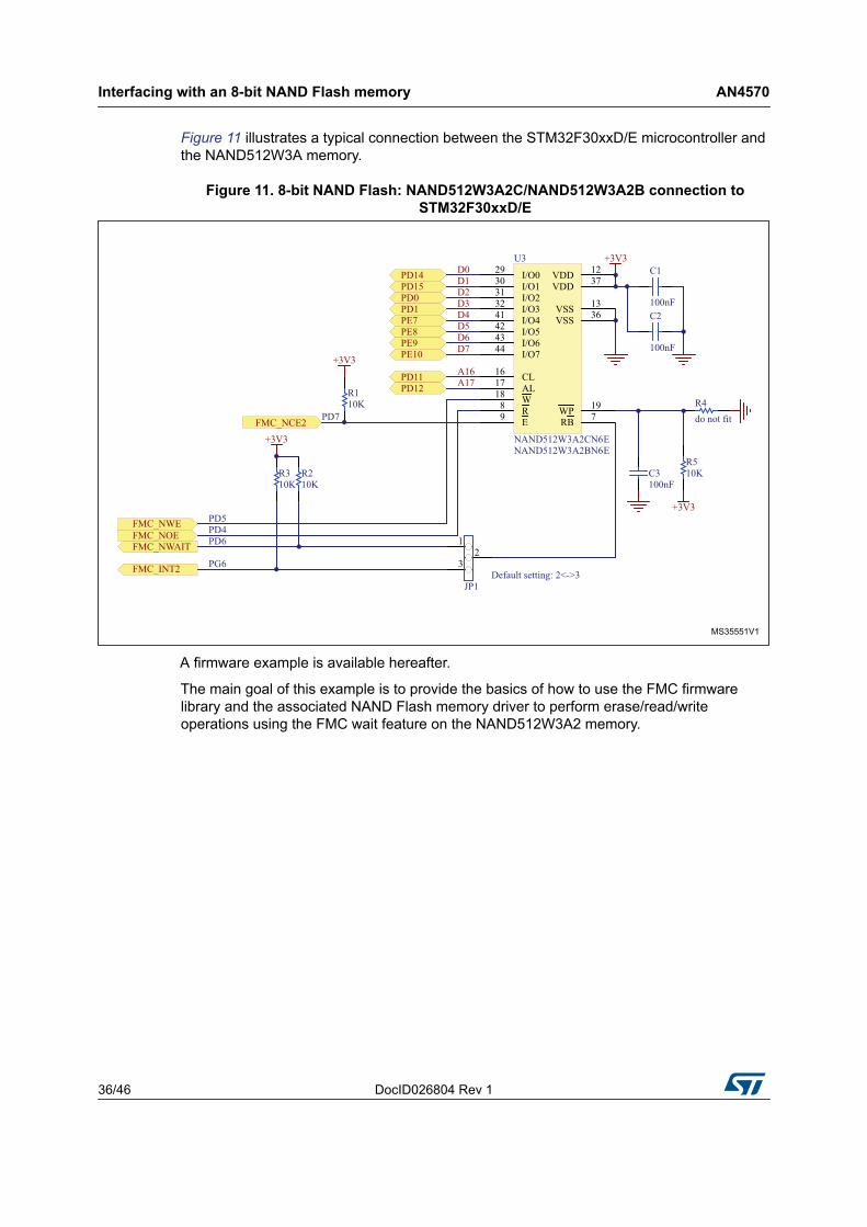
Figure 11 illustrates a typical connection between the STM32F30xxD/E microcontroller and the NAND512W3A memory.
Figure 11. 8-bit NAND Flash: NAND512W3A2C/NAND512W3A2B connection to STM32F30xxD/E
A firmware example is available hereafter.
The main goal of this example is to provide the basics of how to use the FMC firmware library and the associated NAND Flash memory driver to perform erase/read/write operations using the FMC wait feature on the NAND512W3A2 memory.

DocID026804 Rev 1 37/46
AN4570 Interfacing with an 8-bit NAND Flash memory
45
/* Includes ------------------------------------------------------------------*/
#include "stm32f3xx_hal.h"
/* Private define ------------------------------------------------------------*/
#define NAND_DEVICE_ADDR ((uint32_t)0x70000000)
#define BUFFER_SIZE ((uint32_t)16)
#define WRITE_READ_ADDR ((uint32_t)0x20800)
#define NAND_OK 0x00
#define NAND_ERROR 0x01
/* Private variables ---------------------------------------------------------*/
static NAND_HandleTypeDef nandHandle;
static FMC_NAND_PCC_TimingTypeDef Timing;
static NAND_IDTypeDef NAND_ID;
static uint8_t nand_aTxBuffer[BUFFER_SIZE] = {0x00, 0x01, 0x02, 0x03,
0x04, 0x05, 0x06, 0x07,
0x08, 0x09, 0x0A, 0x0B,
0x0C, 0x0D, 0x0E, 0x0F};
static uint8_t nand_aRxBuffer[BUFFER_SIZE]= {0};
/* Private function prototypes -----------------------------------------------*/
extern int main_NAND(void);
int main_NAND(void)
{
NAND_AddressTypedef Address;
nandHandle.Instance = FMC_NAND_DEVICE;
/*##-1- Configure the NAND device###########################################*/
/*NAND Configuration */
Timing.SetupTime = 0;
Timing.WaitSetupTime = 2;
Timing.HoldSetupTime = 1;
Timing.HiZSetupTime = 0;
nandHandle.Init.NandBank = FMC_NAND_BANK2;
nandHandle.Init.Waitfeature = FMC_NAND_PCC_WAIT_FEATURE_ENABLE;
Interfacing with an 8-bit NAND Flash memory AN4570
38/46 DocID026804 Rev 1
nandHandle.Init.MemoryDataWidth = FMC_NAND_PCC_MEM_BUS_WIDTH_8;
nandHandle.Init.EccComputation = FMC_NAND_ECC_ENABLE;
nandHandle.Init.ECCPageSize = FMC_NAND_ECC_PAGE_SIZE_512BYTE;
nandHandle.Init.TCLRSetupTime = 0;
nandHandle.Init.TARSetupTime = 0;
nandHandle.Info.BlockNbr = 0x04;
nandHandle.Info.BlockSize = 0x20;
nandHandle.Info.ZoneSize = 0x400;
nandHandle.Info.PageSize = 0x200;
nandHandle.Info.SpareAreaSize = 0x10;
/* NAND controller initialization */
if(HAL_NAND_Init(&nandHandle, &Timing, &Timing) != HAL_OK)
{
return NAND_ERROR;
}
/*##-2- Read & check the NAND device IDs####################################*/
/* Initialize the ID structure */
NAND_ID.Maker_Id = (uint16_t)0x00;
NAND_ID.Device_Id = (uint16_t)0x00;
NAND_ID.Third_Id = (uint16_t)0x00;
NAND_ID.Fourth_Id = (uint16_t)0x00;
/* Read the NAND memory ID */
if(HAL_NAND_Read_ID(&nandHandle, &NAND_ID) != HAL_OK)
{
return NAND_ERROR;
}
/*##-3- Erase NAND memory###################################################*/
Address.Page = 3;
Address.Zone = 1;
Address.Block = 5;
/* Send NAND erase block operation */
if (HAL_NAND_Erase_Block(&nandHandle, &Address) != HAL_OK)
{
return NAND_ERROR;
}
/*##-4- NAND memory read/write access######################################*/

DocID026804 Rev 1 39/46
AN4570 Interfacing with an 8-bit NAND Flash memory
45
/* Write data to the NAND memory */
if (HAL_NAND_Write_Page(&nandHandle,
&Address,
nand_aTxBuffer,
1) != HAL_OK)
{
return NAND_ERROR;
}
/* Read back data from the NAND memory */
if (HAL_NAND_Read_Page(&nandHandle,
&Address,
nand_aRxBuffer,
1) != HAL_OK)
{
return NAND_ERROR;
}
return NAND_OK;
}
/**
* @brief Initializes the NAND MSP.
* @param None
* @retval None
*/
void HAL_NAND_MspInit(NAND_HandleTypeDef *hnand)
{
GPIO_InitTypeDef GPIO_Init_Structure;
/* Enable FMC clock */
__FMC_CLK_ENABLE();
/* Enable GPIOs clock */
__GPIOD_CLK_ENABLE();
__GPIOE_CLK_ENABLE();
__GPIOG_CLK_ENABLE();
/* Common GPIO configuration */
GPIO_Init_Structure.Mode = GPIO_MODE_AF_PP;
GPIO_Init_Structure.Pull = GPIO_NOPULL;
GPIO_Init_Structure.Speed = GPIO_SPEED_HIGH;
GPIO_Init_Structure.Alternate = GPIO_AF12_FMC;
/* Data D0->D7 */

Interfacing with an 8-bit NAND Flash memory AN4570
40/46 DocID026804 Rev 1
GPIO_Init_Structure.Pin = GPIO_PIN_0 | GPIO_PIN_1 | GPIO_PIN_14 |GPIO_PIN_15;
HAL_GPIO_Init(GPIOD, &GPIO_Init_Structure);
GPIO_Init_Structure.Pin = GPIO_PIN_7 | GPIO_PIN_8 | GPIO_PIN_9 |GPIO_PIN_10;
HAL_GPIO_Init(GPIOE, &GPIO_Init_Structure);
/* Address Command Latch Enable - Address Latch Enable */
GPIO_Init_Structure.Pin = GPIO_PIN_11 | GPIO_PIN_12;
HAL_GPIO_Init(GPIOD, &GPIO_Init_Structure);
/* NWE pin configuration */
GPIO_Init_Structure.Pin = GPIO_PIN_5;
HAL_GPIO_Init(GPIOD, &GPIO_Init_Structure);
/* NOE pin configuration */
GPIO_Init_Structure.Pin = GPIO_PIN_4;
HAL_GPIO_Init(GPIOD, &GPIO_Init_Structure);
/* NCE2 pin configuration */
GPIO_Init_Structure.Pin = GPIO_PIN_7;
HAL_GPIO_Init(GPIOD, &GPIO_Init_Structure);
/* NWAIT NAND pin configuration */
GPIO_Init_Structure.Pin = GPIO_PIN_6;
GPIO_Init_Structure.Mode = GPIO_MODE_AF_PP;
GPIO_Init_Structure.Pull = GPIO_PULLUP;
GPIO_Init_Structure.Alternate = GPIO_AF12_FMC;
HAL_GPIO_Init(GPIOD, &GPIO_Init_Structure);
/* INT2 NAND pin configuration */
GPIO_Init_Structure.Pin = GPIO_PIN_6;
GPIO_Init_Structure.Mode = GPIO_MODE_INPUT;
GPIO_Init_Structure.Pull = GPIO_PULLUP;
HAL_GPIO_Init(GPIOG, &GPIO_Init_Structure);
}
DocID026804 Rev 1 41/46
AN4570 Interfacing with an 8-bit NAND Flash memory
45
4.4 Error correction code computation
4.4.1 Error correction code (ECC) computation overviewThe FMC NAND Flash controller includes two pieces of error correction code computation hardware, one for each NAND Flash memory block.
The ECC can be performed for page sizes of 256, 512, 1024, 2048, 4096 or 8192 bytes, depending on the ECC page size configured by the user. Depending on the configured page size, the ECC code will be 22, 24, 26, 28, 30 or 32 bits.
To even improve the error coverage, the user can read/write the NAND Flash page with a reduced ECC page size. This is possible when starting and stopping the ECC computation after the desired number of bytes to check. In this case, the ECC code is only calculated for the bytes written and read.
The error correction code algorithm implemented in the FMC can perform 1-bit error correction and 2-bit error detection per page read from or written to the NAND Flash memory. It is based on the Hamming algorithm and consists in calculating the row and column parity.
4.4.2 Error detection
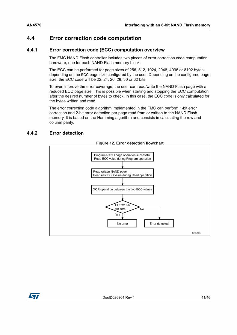
Figure 12. Error detection flowchart
Program NAND page operation successfulRead ECC value during Program operation
Read written NAND pageRead new ECC value during Read operation
XOR operation between the two ECC values
All ECC bitsare zero
Yes
No
No error Error detected
ai15185
Interfacing with an 8-bit NAND Flash memory AN4570
42/46 DocID026804 Rev 1
When an error occurs during the write operation, this error is either correctable or uncorrectable depending on the ECC XOR operation:• Case of a correctable error
The ECC XOR operation contains 11-bit data at 1. And each pair parity is 0x10 or 0x01.• Case of an ECC error
The ECC XOR operation contains only one bit at 1.• Case of an uncorrectable error
The ECC XOR operation is random data. In this case the page data cannot be corrected.
Based on the flowchart shown in Figure 12, the correction software is easy to implement.
The first step consists in detecting whether an error occurred during the write operation. If that was the case, the second step consists in determining if the error is correctable or not. If it is correctable, then the third step consists in correcting the error.
The error correction is based on the second ECC generated after the read operation. The error location can be identified from this code. Usually, the following data are extracted from the ECC:
P1024, P512, P256, P128, P64, P32, P16, P8, P4, P2, P1, where Px are the line and column parity.
In case of an 8-bit memory, P4, P2, P1 define the error bit position. And P1024, P512, P256, P128, P64, P32, P16, P8 define the error byte position.

DocID026804 Rev 1 43/46
AN4570 STM32F30xxD/E FMC configuration in 100-pin packages
45
5 STM32F30xxD/E FMC configuration in 100-pin packages
The FMC is present in devices delivered in both 144-pin and 100-pin packages. For devices in 100-pin packages, however, only some FMC banks can be used because not all pins are available.
5.1 Interfacing the FMC with a NAND Flash memoryIn devices that come in 100-pin packages, only Bank2 can be used to interface the FMC with an 8-/16-bit NAND Flash memory. This is because the NCE3 pin is not available in these packages.
Likewise, no interrupt can be used because the two interrupt pins INT2 and INT3 are not available in 100-pin packages.
Table 10 shows how to connect an 8-/16-bit NAND Flash memory to the FMC peripheral of devices delivered in 100-pin packages.
Table 10. NAND Flash memory connection to the FMC 8-/16-bit NAND memory pins FMC pins 100-pin package
E NCE2/NCE3 NCE2
R NOE NOE
W NWE NWE
AL A17 A17
CL A16 A16
R/B NWAIT/INT2/INT3 NWAIT
I/O0-I/O7 D0-D7 D0-D7
I/O8-I/O15 D8-D15 D8-D15
STM32F30xxD/E FMC configuration in 100-pin packages AN4570
44/46 DocID026804 Rev 1
5.2 Interfacing the FMC with a NOR Flash memoryIn devices that come in 100-pin packages, only Bank 1 (NOR/PSRAM 1) can be used to interface with a NOR Flash memory. This is because the NE2, NE3 and NE4 pins are not available in these packages.
Likewise, the A0-A15 pins are not available, so the NOR Flash controller should be used in multiplexed mode to use the data bus for both address and data.
In 8-bit muxed mode, the FMC address signals A[15:8] are available on the AD[15:8] pins.
Table 11 shows how to connect a NOR Flash memory to the FMC peripheral of devices delivered in 100-pin packages.
Table 11. NOR Flash memory connection to the FMC 8-/16-bit NOR/PSRAM pins FMC pins 100-pin package
A[15:0] A[15:0] DA[15:0]
A[23:16] A[23:16] A[23:16]
DQ[15:0] D[15:0] D[15:0]
W NWE NWE
E NE1/NE2/NE3/NE4 NE1
G NOE NOE
ADV NADV NADV
R/B NWAIT NWAIT
UB, LB NBL[1:0] NBL[1:0]

DocID026804 Rev 1 45/46
AN4570 Revision history
45
6 Revision history
Table 12. Document revision history Date Revision Changes
28-Jan-2015 1 Initial release.
AN4570
46/46 DocID026804 Rev 1
IMPORTANT NOTICE – PLEASE READ CAREFULLY
STMicroelectronics NV and its subsidiaries (“ST”) reserve the right to make changes, corrections, enhancements, modifications, and improvements to ST products and/or to this document at any time without notice. Purchasers should obtain the latest relevant information on ST products before placing orders. ST products are sold pursuant to ST’s terms and conditions of sale in place at the time of order acknowledgement.
Purchasers are solely responsible for the choice, selection, and use of ST products and ST assumes no liability for application assistance or the design of Purchasers’ products.
No license, express or implied, to any intellectual property right is granted by ST herein.
Resale of ST products with provisions different from the information set forth herein shall void any warranty granted by ST for such product.
ST and the ST logo are trademarks of ST. All other product or service names are the property of their respective owners.
Information in this document supersedes and replaces information previously supplied in any prior versions of this document.
© 2015 STMicroelectronics – All rights reserved