an11991 - nxp
TRANSCRIPT
AN11991 Front end module (including PA, RX/TX switch) for IoT applications using BGA6130 as PA and BAP64-02 as switch Rev. 1 — 31 August 2017 Application note
Document information Info Content Keywords RX/TX, Switch, BAP64-02, BGA6130, LNA
Abstract This document explains the RX/TX pin diode switch evaluation board
Ordering info BGA6130, BAP64-02 starter kit OM17065, 12nc 9340 713 99598
Contact information For more information, please visit: http://www.nxp.com
NXP Semiconductors AN11991
Front end module (including PA, RX/TX switch) for IoT applications using BGA6130 as PA and BAP64-02 as switch
AN11991 All information provided in this document is subject to legal disclaimers. © NXP B.V. 2016. All rights reserved.
Application note Rev. 1 — 31 August 2017 2 of 61
Contact information For more information, please visit: http://www.nxp.com For sales office addresses, please send an email to: [email protected]
Revision history Rev Date Description 1.0 20170831
First publication
NXP Semiconductors AN11991
Front end module (including PA, RX/TX switch) for IoT applications using BGA6130 as PA and BAP64-02 as switch
AN11991 All information provided in this document is subject to legal disclaimers. © NXP B.V. 2016. All rights reserved.
Application note Rev. 1 — 31 August 2017 3 of 61
1. Introduction IoT applications needs Front end modules (PA + RX/TX switch) which can be realized using NXP’s BGA6130 and BAP64-02. A pair of PIN diodes (BAP64-02) are used in a RX/TX switch configuration and an MPA (BGA6130) is used as a gain stage to deliver a certain amount of RF power. A typical application could be an IoT range extender.
Two evaluation boards are designed to evaluate the performance of the PIN diodes with or without the use of an MPA.
The EVB contains the following parts:
• NXP Semiconductors BAP64-02 diodes
• Optional NXP Semiconductors BGA6130 amplifier
• A low pass Chebyshev filter
• Decoupling of the power supply and control signals
In this document, the application diagram, board layout, bill of materials, and typical results are given. Fig 1 shows a picture of the RX/TX switch without an MPA. Fig 2 shows a picture of the RX/TX switch with an additional MPA.
Fig 1. RX/TX Switch evaluation board
Fig 2. RX/TX Switch evaluation board with BGA6130
NXP Semiconductors AN11991
Front end module (including PA, RX/TX switch) for IoT applications using BGA6130 as PA and BAP64-02 as switch
AN11991 All information provided in this document is subject to legal disclaimers. © NXP B.V. 2016. All rights reserved.
Application note Rev. 1 — 31 August 2017 4 of 61
2. General description The nowadays modern transceivers or radios require a way to switch the antenna to either a transmitter output or a receiver input. The switch should be robust enough to handle the RF power of the transmitter as well as exhibiting low insertion loss in the receive mode to reduce the added noise figure to the LNA.
While mechanical switches typically have a lower “ON” resistance and generate less harmonic distortion, they are larger in size, slow switching and more expensive and therefore in many cases not suitable.
The solution to overcome these drawbacks is PIN diode technology. These diodes are developed to use as an RF switch. Their “ON” resistance varies from less than a few ohms to more than several kilo ohms in the “OFF” state. These typical characteristics make them well suitable to use as an RX/TX switch.
An RX/TX switch can be constructed by using a PIN diode in series at the TX path and a parallel PIN diode construction at the RX path to avoid excessive RF power at the input of the LNA while in TX mode.
In certain applications e.g. IoT, repeaters, signal booster etc. an additional MPA is needed. A separate EVB (Evaluation Board) is available to evaluate the RX/TX switch in combination with an MPA. Table 1 gives an overview of the different configurations. In this application note, all these different configurations are evaluated.
Table 1. Configuration overview Configuration Narrow
band Broad band
Filter BGA6130 RX power consumption
Comments
1 • • None Details see Par. 3 2 • None
3 • • *
4 • *
5 • • • None Details see Par. 4 6 • • None
7 • • • *
8 • • * *power consumption depends on bias setting The application without the MPA is described in chapter 3. Chapter 4 describes the application with the MPA. Both chapters contains the application description and measurement results. The customer evaluation kit “starter kit” OM17065 contains the configuration 2 (only switch), configuration 6 (switch + PA), empty boards and loose sample.
NXP Semiconductors AN11991
Front end module (including PA, RX/TX switch) for IoT applications using BGA6130 as PA and BAP64-02 as switch
AN11991 All information provided in this document is subject to legal disclaimers. © NXP B.V. 2016. All rights reserved.
Application note Rev. 1 — 31 August 2017 5 of 61
3. RX/TX switch evaluation board The RX/TX switch evaluation board simplifies the evaluation of the BAP64-02 in a RX/TX configuration. The evaluation board enables testing of the devices RF performance and requires no additional support circuitry. The board is fully assembled with the two BAP64-02 PIN diodes and the necessary bias circuitry. The board is contains three SMA connectors for input and output connection to RF test equipment. The BAP64-02 RX/TX switch operates with a 3.3 V single supply and consumes typical 5 or 15 mA in TX mode depending on the bias resistor. The circuit consumes zero current in RX mode (narrow bandwidth version).
Typical characteristics:
• High output power capability
• Zero current during receive mode (narrow bandwidth version)
• Low component count (depends on customer application)
NXP Semiconductors AN11991
Front end module (including PA, RX/TX switch) for IoT applications using BGA6130 as PA and BAP64-02 as switch
AN11991 All information provided in this document is subject to legal disclaimers. © NXP B.V. 2016. All rights reserved.
Application note Rev. 1 — 31 August 2017 6 of 61
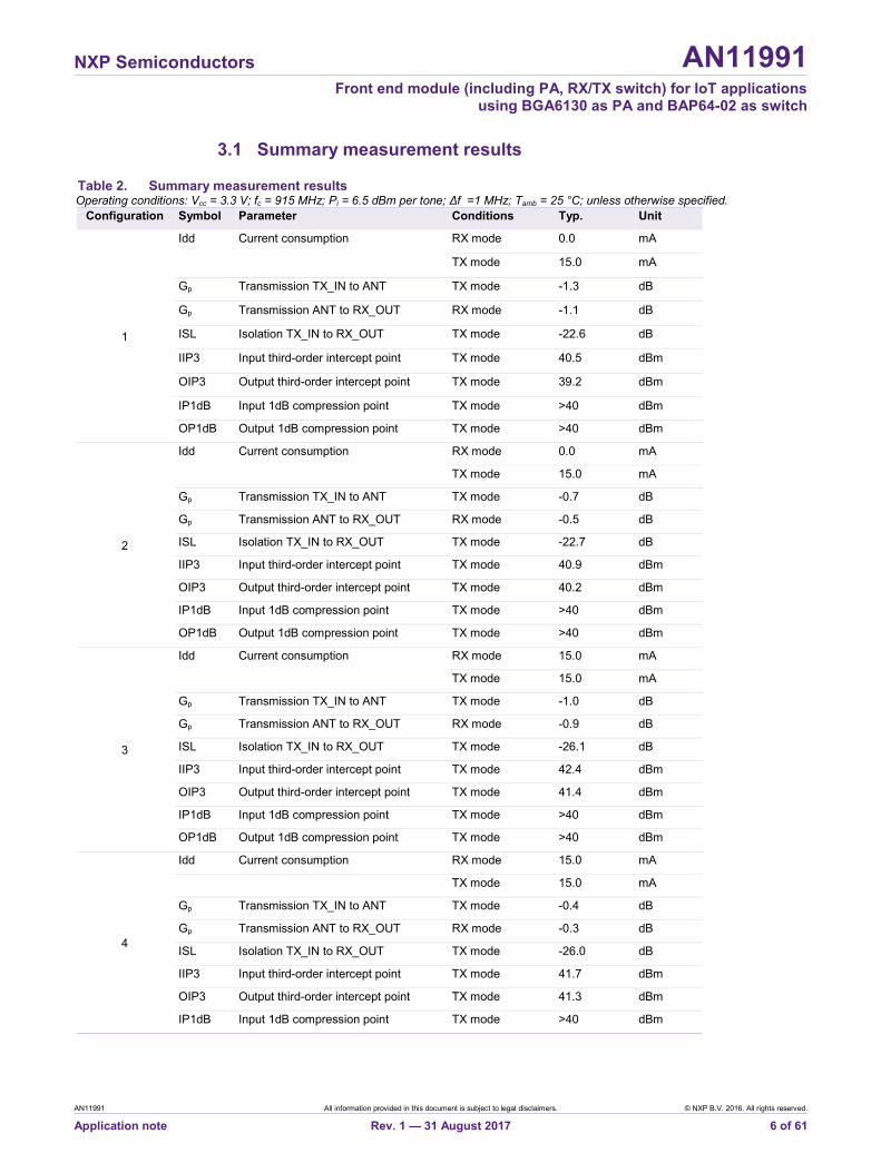
3.1 Summary measurement results
Table 2. Summary measurement results Operating conditions: Vcc = 3.3 V; fc = 915 MHz; Pi = 6.5 dBm per tone; Δf =1 MHz; Tamb = 25 °C; unless otherwise specified.
Configuration Symbol Parameter Conditions Typ. Unit
1
Idd Current consumption RX mode 0.0 mA
TX mode 15.0 mA
Gp Transmission TX_IN to ANT TX mode -1.3 dB
Gp Transmission ANT to RX_OUT RX mode -1.1 dB
ISL Isolation TX_IN to RX_OUT TX mode -22.6 dB
IIP3 Input third-order intercept point TX mode 40.5 dBm
OIP3 Output third-order intercept point TX mode 39.2 dBm
IP1dB Input 1dB compression point TX mode >40 dBm
OP1dB Output 1dB compression point TX mode >40 dBm
2
Idd Current consumption RX mode 0.0 mA
TX mode 15.0 mA
Gp Transmission TX_IN to ANT TX mode -0.7 dB
Gp Transmission ANT to RX_OUT RX mode -0.5 dB
ISL Isolation TX_IN to RX_OUT TX mode -22.7 dB
IIP3 Input third-order intercept point TX mode 40.9 dBm
OIP3 Output third-order intercept point TX mode 40.2 dBm
IP1dB Input 1dB compression point TX mode >40 dBm
OP1dB Output 1dB compression point TX mode >40 dBm
3
Idd Current consumption RX mode 15.0 mA
TX mode 15.0 mA
Gp Transmission TX_IN to ANT TX mode -1.0 dB
Gp Transmission ANT to RX_OUT RX mode -0.9 dB
ISL Isolation TX_IN to RX_OUT TX mode -26.1 dB
IIP3 Input third-order intercept point TX mode 42.4 dBm
OIP3 Output third-order intercept point TX mode 41.4 dBm
IP1dB Input 1dB compression point TX mode >40 dBm
OP1dB Output 1dB compression point TX mode >40 dBm
4
Idd Current consumption RX mode 15.0 mA
TX mode 15.0 mA
Gp Transmission TX_IN to ANT TX mode -0.4 dB
Gp Transmission ANT to RX_OUT RX mode -0.3 dB
ISL Isolation TX_IN to RX_OUT TX mode -26.0 dB
IIP3 Input third-order intercept point TX mode 41.7 dBm
OIP3 Output third-order intercept point TX mode 41.3 dBm
IP1dB Input 1dB compression point TX mode >40 dBm

NXP Semiconductors AN11991
Front end module (including PA, RX/TX switch) for IoT applications using BGA6130 as PA and BAP64-02 as switch
AN11991 All information provided in this document is subject to legal disclaimers. © NXP B.V. 2016. All rights reserved.
Application note Rev. 1 — 31 August 2017 7 of 61
Configuration Symbol Parameter Conditions Typ. Unit
OP1dB Output 1dB compression point TX mode >40 dBm
NXP Semiconductors AN11991
Front end module (including PA, RX/TX switch) for IoT applications using BGA6130 as PA and BAP64-02 as switch
AN11991 All information provided in this document is subject to legal disclaimers. © NXP B.V. 2016. All rights reserved.
Application note Rev. 1 — 31 August 2017 8 of 61
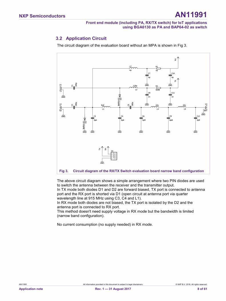
3.2 Application Circuit The circuit diagram of the evaluation board without an MPA is shown in Fig 3.
The above circuit diagram shows a simple arrangement where two PIN diodes are used to switch the antenna between the receiver and the transmitter output. In TX mode both diodes D1 and D2 are forward biased, TX port is connected to antenna port and the RX port is shorted via D1 (open circuit at antenna port via quarter wavelength line at 915 MHz using C3, C4 and L1). In RX mode both diodes are not biased, the TX port is isolated by the D2 and the antenna port is connected to RX port. This method doesn't need supply voltage in RX mode but the bandwidth is limited (narrow band configuration). No current consumption (no supply needed) in RX mode.
Fig 3. Circuit diagram of the RX/TX Switch evaluation board narrow band configuration
NXP Semiconductors AN11991
Front end module (including PA, RX/TX switch) for IoT applications using BGA6130 as PA and BAP64-02 as switch
AN11991 All information provided in this document is subject to legal disclaimers. © NXP B.V. 2016. All rights reserved.
Application note Rev. 1 — 31 August 2017 9 of 61
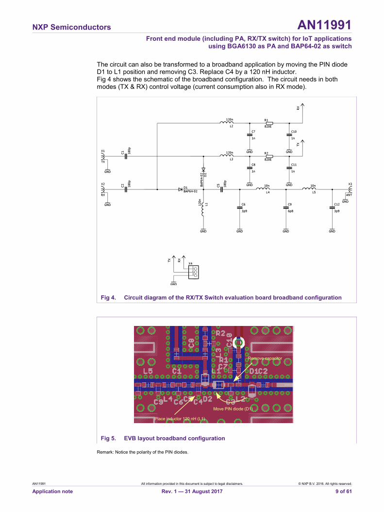
The circuit can also be transformed to a broadband application by moving the PIN diode D1 to L1 position and removing C3. Replace C4 by a 120 nH inductor. Fig 4 shows the schematic of the broadband configuration. The circuit needs in both modes (TX & RX) control voltage (current consumption also in RX mode).
Remark: Notice the polarity of the PIN diodes.
Fig 4. Circuit diagram of the RX/TX Switch evaluation board broadband configuration
Fig 5. EVB layout broadband configuration
Place inductor 120 nH (L1)
Move PIN diode (D1)
Remove capacitor
NXP Semiconductors AN11991
Front end module (including PA, RX/TX switch) for IoT applications using BGA6130 as PA and BAP64-02 as switch
AN11991 All information provided in this document is subject to legal disclaimers. © NXP B.V. 2016. All rights reserved.
Application note Rev. 1 — 31 August 2017 10 of 61
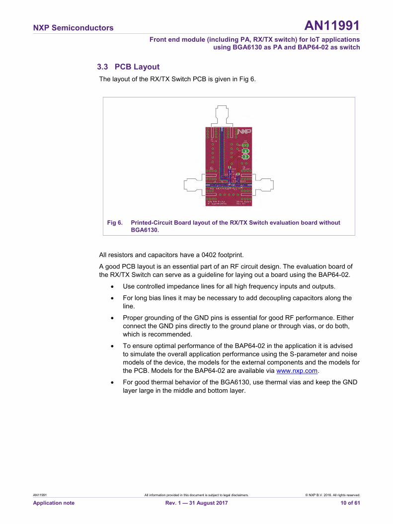
3.3 PCB Layout The layout of the RX/TX Switch PCB is given in Fig 6.
Fig 6. Printed-Circuit Board layout of the RX/TX Switch evaluation board without BGA6130.
All resistors and capacitors have a 0402 footprint.
A good PCB layout is an essential part of an RF circuit design. The evaluation board of the RX/TX Switch can serve as a guideline for laying out a board using the BAP64-02.
• Use controlled impedance lines for all high frequency inputs and outputs.
• For long bias lines it may be necessary to add decoupling capacitors along the line.
• Proper grounding of the GND pins is essential for good RF performance. Either connect the GND pins directly to the ground plane or through vias, or do both, which is recommended.
• To ensure optimal performance of the BAP64-02 in the application it is advised to simulate the overall application performance using the S-parameter and noise models of the device, the models for the external components and the models for the PCB. Models for the BAP64-02 are available via www.nxp.com.
• For good thermal behavior of the BGA6130, use thermal vias and keep the GND layer large in the middle and bottom layer.
NXP Semiconductors AN11991
Front end module (including PA, RX/TX switch) for IoT applications using BGA6130 as PA and BAP64-02 as switch
AN11991 All information provided in this document is subject to legal disclaimers. © NXP B.V. 2016. All rights reserved.
Application note Rev. 1 — 31 August 2017 11 of 61
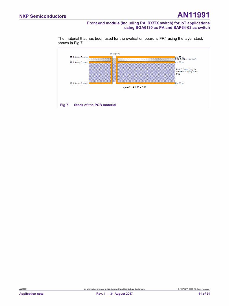
The material that has been used for the evaluation board is FR4 using the layer stack shown in Fig 7.
Fig 7. Stack of the PCB material
NXP Semiconductors AN11991
Front end module (including PA, RX/TX switch) for IoT applications using BGA6130 as PA and BAP64-02 as switch
AN11991 All information provided in this document is subject to legal disclaimers. © NXP B.V. 2016. All rights reserved.
Application note Rev. 1 — 31 August 2017 12 of 61
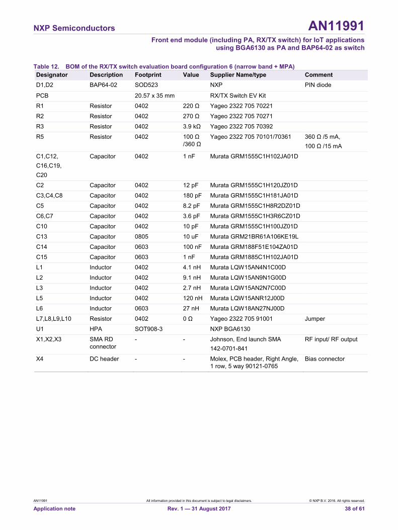
3.4 Bill of materials With the evaluation board, several configurations are possible. The different configurations are identified as follows:
Table 3. BOM of the RX/TX switch evaluation board configuration 1 (narrow band + low pass filter) Designator Description Footprint Value Supplier Name/type Comment D1,D2 BAP64-02 SOD523 NXP PIN diode
PCB 20.57 x 35 mm RX/TX Switch EV Kit
R2 Resistor 0402 100 Ω /360 Ω
Yageo 2322 705 70101/70361 360 Ω /5 mA, 100 Ω /15 mA
C1,C2,C5 Capacitor 0402 180 pF Murata GRM1555C1H181JA01D
C3,C4 Capacitor 0402 3.6 pF Murata GRM1555C1H3R6CZ01D
C6,C12 Capacitor 0402 3.9 pF Murata GRM1555C1H3R9CZ01D
C8,C11 Capacitor 0402 1 nF Murata GRM1555C1H102JA01D
C9 Capacitor 0402 6.8 pF Murata GRM1555C1H6R8DZ01D
L1 Inductor 0402 9.1 nH Murata LQW15AN9N1G00D
L3 Inductor 0402 120 nH Murata LQW15ANR12J00D
L4,L5 Inductor 0402 10 nH Murata LQW15AN10NG00D
X1,X2,X3 SMA RD connector
- - Johnson, End launch SMA 142-0701-841
RF input/ RF output
X4 DC header - - Molex, PCB header, Right Angle, 1 row, 3 way 90121-0763
Bias connector
Table 4. BOM of the RX/TX switch evaluation board configuration 2 (narrow band) Designator Description Footprint Value Supplier Name/type Comment D1,D2 BAP64-02 SOD523 NXP PIN diode
PCB 20.57 x 35 mm RX/TX Switch EV Kit
R2 Resistor 0402 100 Ω /360 Ω
Yageo 2322 705 70101/70361 360 Ω /5 mA, 100 Ω /15 mA
C1,C2,C5 Capacitor 0402 180 pF Murata GRM1555C1H181JA01D
C3,C4 Capacitor 0402 3.6 pF Murata GRM1555C1H3R6CZ01D
C8,C11 Capacitor 0402 1 nF Murata GRM1555C1H102JA01D
L1 Inductor 0402 9.1 nH Murata LQW15AN9N1G00D
L3 Inductor 0402 120 nH Murata LQW15ANR12J00D
L4,L5 Resistor 0402 0 Ω Yageo 2322 705 91001 Jumper
X1,X2,X3 SMA RD connector
- - Johnson, End launch SMA 142-0701-841
RF input/ RF output
X4 DC header - - Molex, PCB header, Right Angle, 1 row, 3 way 90121-0763
Bias connector
NXP Semiconductors AN11991
Front end module (including PA, RX/TX switch) for IoT applications using BGA6130 as PA and BAP64-02 as switch
AN11991 All information provided in this document is subject to legal disclaimers. © NXP B.V. 2016. All rights reserved.
Application note Rev. 1 — 31 August 2017 13 of 61
Table 5. BOM of the RX/TX switch evaluation board configuration 3 (broadband + low pass filter) Designator Description Footprint Value Supplier Name/type Comment D2 BAP64-02 SOD523 NXP PIN diode
PCB 20.57 x 35 mm RX/TX Switch EV Kit
R1,R2 Resistor 0402 150 Ω /470 Ω
Yageo 2322 705 70151/70471 470 Ω /5 mA, 150 Ω /15 mA
C1,C2,C5 Capacitor 0402 180 pF Murata GRM1555C1H181JA01D
C4 Capacitor 0402 120 nH Murata LQW15ANR12J00D Place inductor at C4 pos.
C6,C12 Capacitor 0402 3.9 pF Murata GRM1555C1H3R9CZ01D
C7,C8,C10,C11
Capacitor 0402 1 nF Murata GRM1555C1H102JA01D
C9 Capacitor 0402 6.8 pF Murata GRM1555C1H6R8DZ01D
L1 Inductor 0402 9.1 nH Murata LQW15AN9N1G00D
L2,L3 Inductor 0402 120 nH Murata LQW15ANR12J00D
L4,L5 Inductor 0402 10 nH Murata LQW15AN10NG00D
X1,X2,X3 SMA RD connector
- - Johnson, End launch SMA 142-0701-841
RF input/ RF output
X4 DC header - - Molex, PCB header, Right Angle, 1 row, 3 way 90121-0763
Bias connector
Table 6. BOM of the RX/TX switch evaluation board configuration 4 (broadband) Designator Description Footprint Value Supplier Name/type Comment D2 BAP64-02 SOD523 NXP PIN diode
PCB 20.57 x 35 mm RX/TX Switch EV Kit
R1,R2 Resistor 0402 150 Ω /470 Ω
Yageo 2322 705 70151/70471 470 Ω /5 mA, 150 Ω /15 mA
C1,C2,C5 Capacitor 0402 180 pF Murata GRM1555C1H181JA01D
C4 Capacitor 0402 120 nH Murata LQW15ANR12J00D Place inductor at C4 pos.
C7,C8,C10,C11
Capacitor 0402 1 nF Murata GRM1555C1H102JA01D
L1 BAP64-02 SOD523 NXP Place BAP64-02 at L1 pos.
L2,L3 Inductor 0402 120 nH Murata LQW15ANR12J00D
L4,L5 Resistor 0402 0 Ω Yageo 2322 705 91001 Jumper
X1,X2,X3 SMA RD connector
- - Johnson, End launch SMA 142-0701-841
RF input/ RF output
X4 DC header - - Molex, PCB header, Right Angle, 1 row, 3 way 90121-0763
Bias connector
NXP Semiconductors AN11991
Front end module (including PA, RX/TX switch) for IoT applications using BGA6130 as PA and BAP64-02 as switch
AN11991 All information provided in this document is subject to legal disclaimers. © NXP B.V. 2016. All rights reserved.
Application note Rev. 1 — 31 August 2017 14 of 61
3.5 Measurement results 3.5.1 S-parameters (3-port)
Because the RX/TX switch contains three RF-ports, it is desirable to have a three ports small signal S-parameter measurement. There are two situations to be analyzed. The RX/TX switch can be set in RX or TX mode. For both situations an S-parameter measurement is performed. The measurements are performed under the following conditions:
- Pin = -30 dBm
- Frequency = 10 – 6000 MHz
- Ambient temperature = 25°C
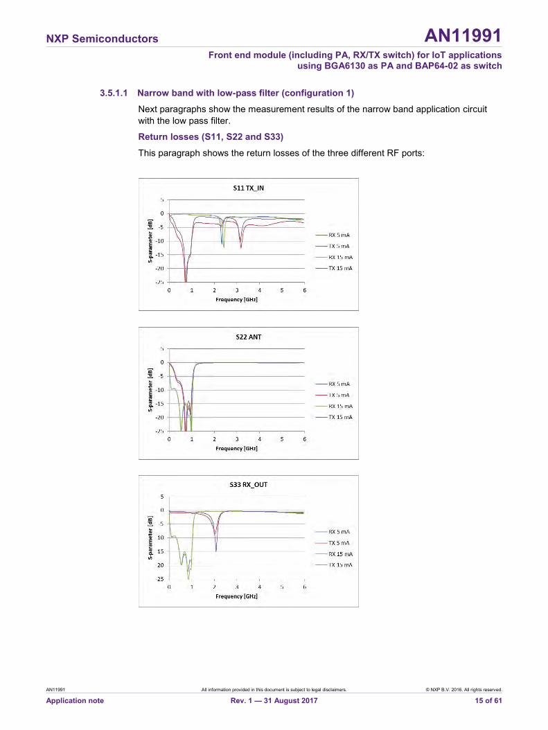
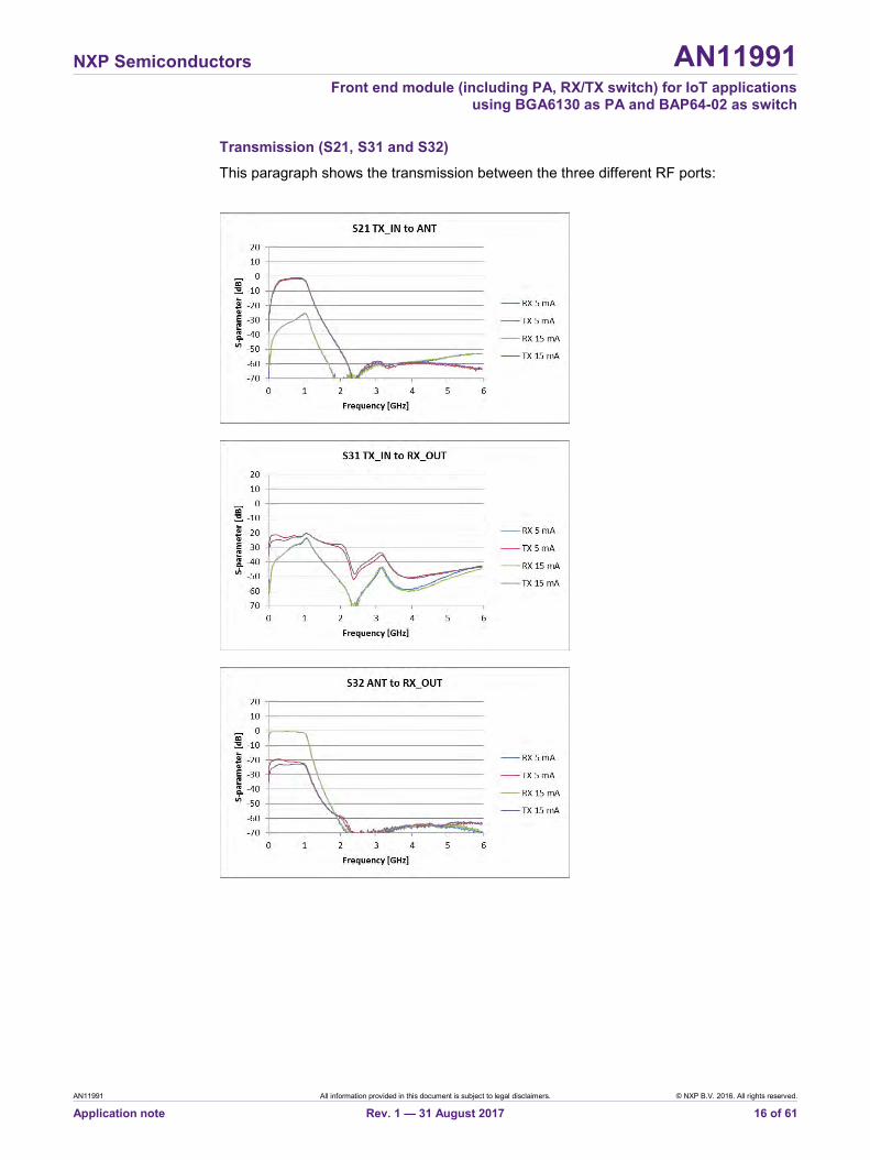
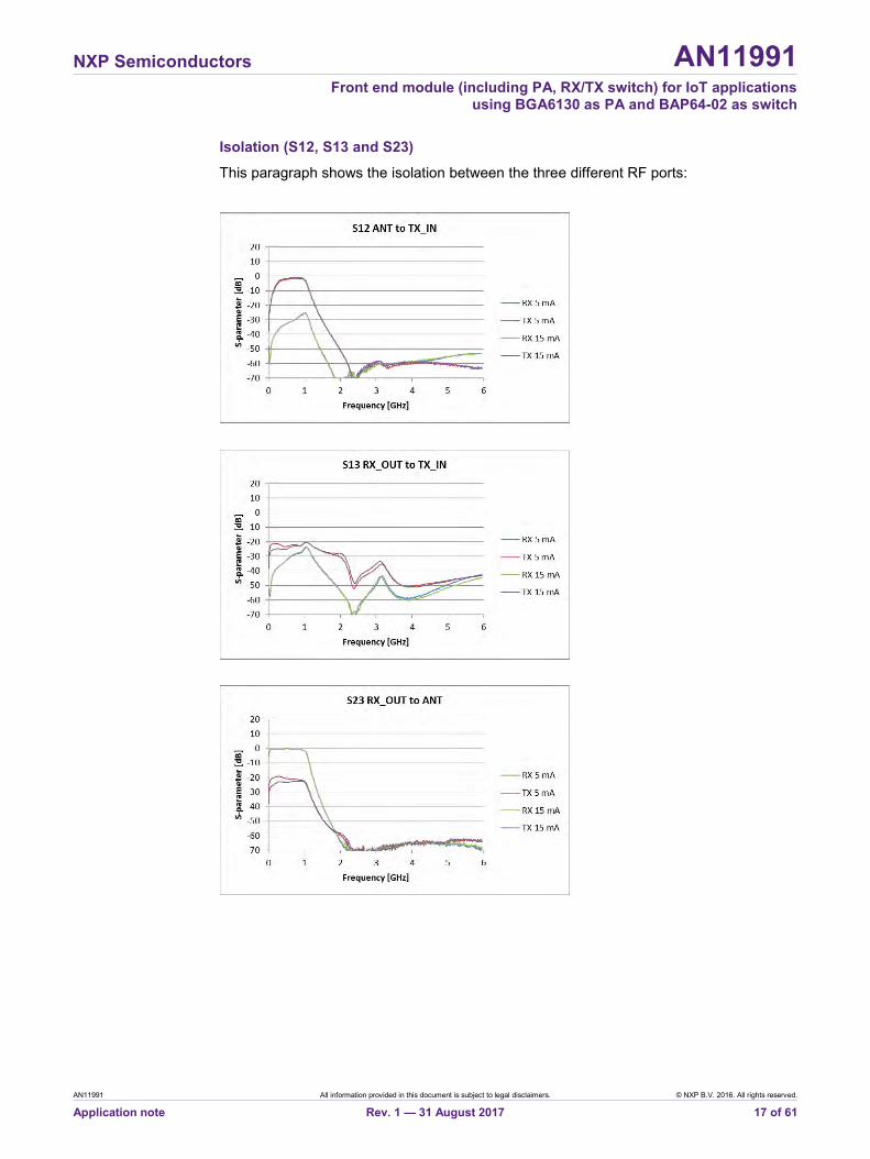
In the TX mode, the RF path between the TX input and the antenna output has a low insertion loss. In the TX mode, there is high isolation between the ANT/TX_IN connection and RX_OUT port.
Next paragraphs shows the S-parameters graphs measured at different PIN diode currents (5 and 15 mA). The graphs shows also the low pass filter response with a cut-off frequency of 1 GHz.
NXP Semiconductors AN11991
Front end module (including PA, RX/TX switch) for IoT applications using BGA6130 as PA and BAP64-02 as switch
AN11991 All information provided in this document is subject to legal disclaimers. © NXP B.V. 2016. All rights reserved.
Application note Rev. 1 — 31 August 2017 15 of 61
3.5.1.1 Narrow band with low-pass filter (configuration 1)
Next paragraphs show the measurement results of the narrow band application circuit with the low pass filter.
Return losses (S11, S22 and S33)
This paragraph shows the return losses of the three different RF ports:
NXP Semiconductors AN11991
Front end module (including PA, RX/TX switch) for IoT applications using BGA6130 as PA and BAP64-02 as switch
AN11991 All information provided in this document is subject to legal disclaimers. © NXP B.V. 2016. All rights reserved.
Application note Rev. 1 — 31 August 2017 16 of 61
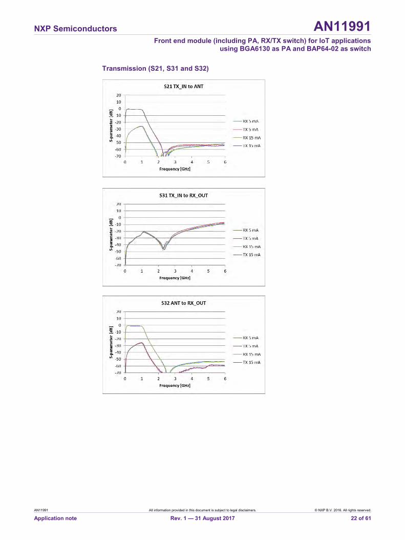
Transmission (S21, S31 and S32)
This paragraph shows the transmission between the three different RF ports:
NXP Semiconductors AN11991
Front end module (including PA, RX/TX switch) for IoT applications using BGA6130 as PA and BAP64-02 as switch
AN11991 All information provided in this document is subject to legal disclaimers. © NXP B.V. 2016. All rights reserved.
Application note Rev. 1 — 31 August 2017 17 of 61
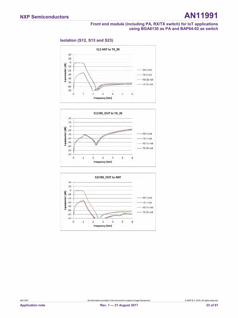
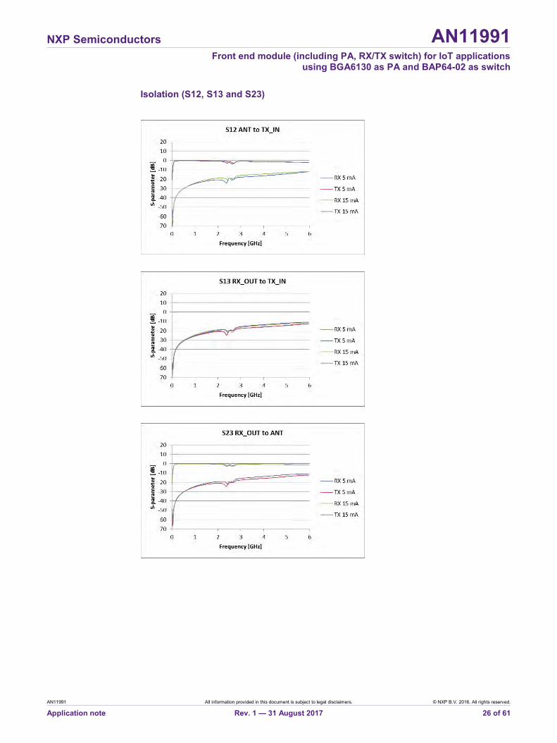
Isolation (S12, S13 and S23)
This paragraph shows the isolation between the three different RF ports:
NXP Semiconductors AN11991
Front end module (including PA, RX/TX switch) for IoT applications using BGA6130 as PA and BAP64-02 as switch
AN11991 All information provided in this document is subject to legal disclaimers. © NXP B.V. 2016. All rights reserved.
Application note Rev. 1 — 31 August 2017 18 of 61
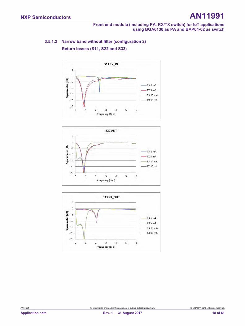
3.5.1.2 Narrow band without filter (configuration 2)
Return losses (S11, S22 and S33)
NXP Semiconductors AN11991
Front end module (including PA, RX/TX switch) for IoT applications using BGA6130 as PA and BAP64-02 as switch
AN11991 All information provided in this document is subject to legal disclaimers. © NXP B.V. 2016. All rights reserved.
Application note Rev. 1 — 31 August 2017 19 of 61
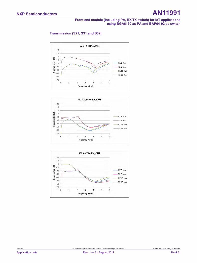
Transmission (S21, S31 and S32)
NXP Semiconductors AN11991
Front end module (including PA, RX/TX switch) for IoT applications using BGA6130 as PA and BAP64-02 as switch
AN11991 All information provided in this document is subject to legal disclaimers. © NXP B.V. 2016. All rights reserved.
Application note Rev. 1 — 31 August 2017 20 of 61
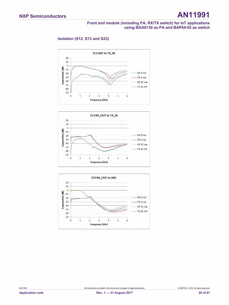
Isolation (S12, S13 and S23)
NXP Semiconductors AN11991
Front end module (including PA, RX/TX switch) for IoT applications using BGA6130 as PA and BAP64-02 as switch
AN11991 All information provided in this document is subject to legal disclaimers. © NXP B.V. 2016. All rights reserved.
Application note Rev. 1 — 31 August 2017 21 of 61
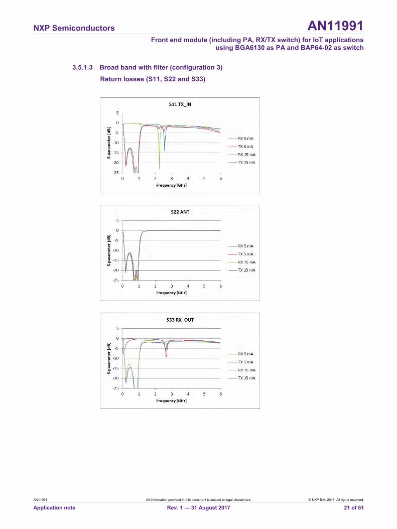
3.5.1.3 Broad band with filter (configuration 3)
Return losses (S11, S22 and S33)
NXP Semiconductors AN11991
Front end module (including PA, RX/TX switch) for IoT applications using BGA6130 as PA and BAP64-02 as switch
AN11991 All information provided in this document is subject to legal disclaimers. © NXP B.V. 2016. All rights reserved.
Application note Rev. 1 — 31 August 2017 22 of 61
Transmission (S21, S31 and S32)
NXP Semiconductors AN11991
Front end module (including PA, RX/TX switch) for IoT applications using BGA6130 as PA and BAP64-02 as switch
AN11991 All information provided in this document is subject to legal disclaimers. © NXP B.V. 2016. All rights reserved.
Application note Rev. 1 — 31 August 2017 23 of 61
Isolation (S12, S13 and S23)
NXP Semiconductors AN11991
Front end module (including PA, RX/TX switch) for IoT applications using BGA6130 as PA and BAP64-02 as switch
AN11991 All information provided in this document is subject to legal disclaimers. © NXP B.V. 2016. All rights reserved.
Application note Rev. 1 — 31 August 2017 24 of 61
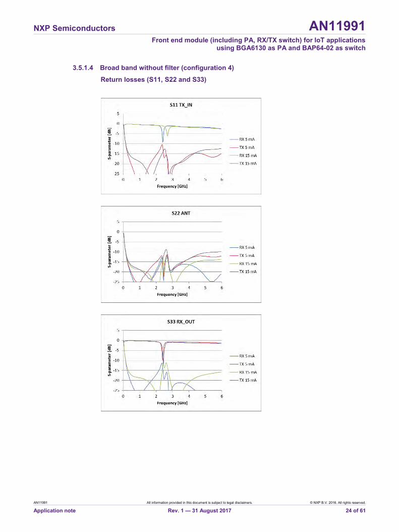
3.5.1.4 Broad band without filter (configuration 4)
Return losses (S11, S22 and S33)
NXP Semiconductors AN11991
Front end module (including PA, RX/TX switch) for IoT applications using BGA6130 as PA and BAP64-02 as switch
AN11991 All information provided in this document is subject to legal disclaimers. © NXP B.V. 2016. All rights reserved.
Application note Rev. 1 — 31 August 2017 25 of 61
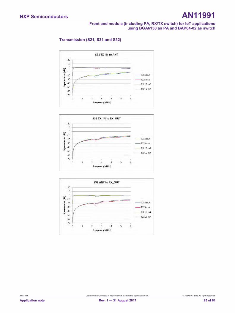
Transmission (S21, S31 and S32)
NXP Semiconductors AN11991
Front end module (including PA, RX/TX switch) for IoT applications using BGA6130 as PA and BAP64-02 as switch
AN11991 All information provided in this document is subject to legal disclaimers. © NXP B.V. 2016. All rights reserved.
Application note Rev. 1 — 31 August 2017 26 of 61
Isolation (S12, S13 and S23)
NXP Semiconductors AN11991
Front end module (including PA, RX/TX switch) for IoT applications using BGA6130 as PA and BAP64-02 as switch
AN11991 All information provided in this document is subject to legal disclaimers. © NXP B.V. 2016. All rights reserved.
Application note Rev. 1 — 31 August 2017 27 of 61
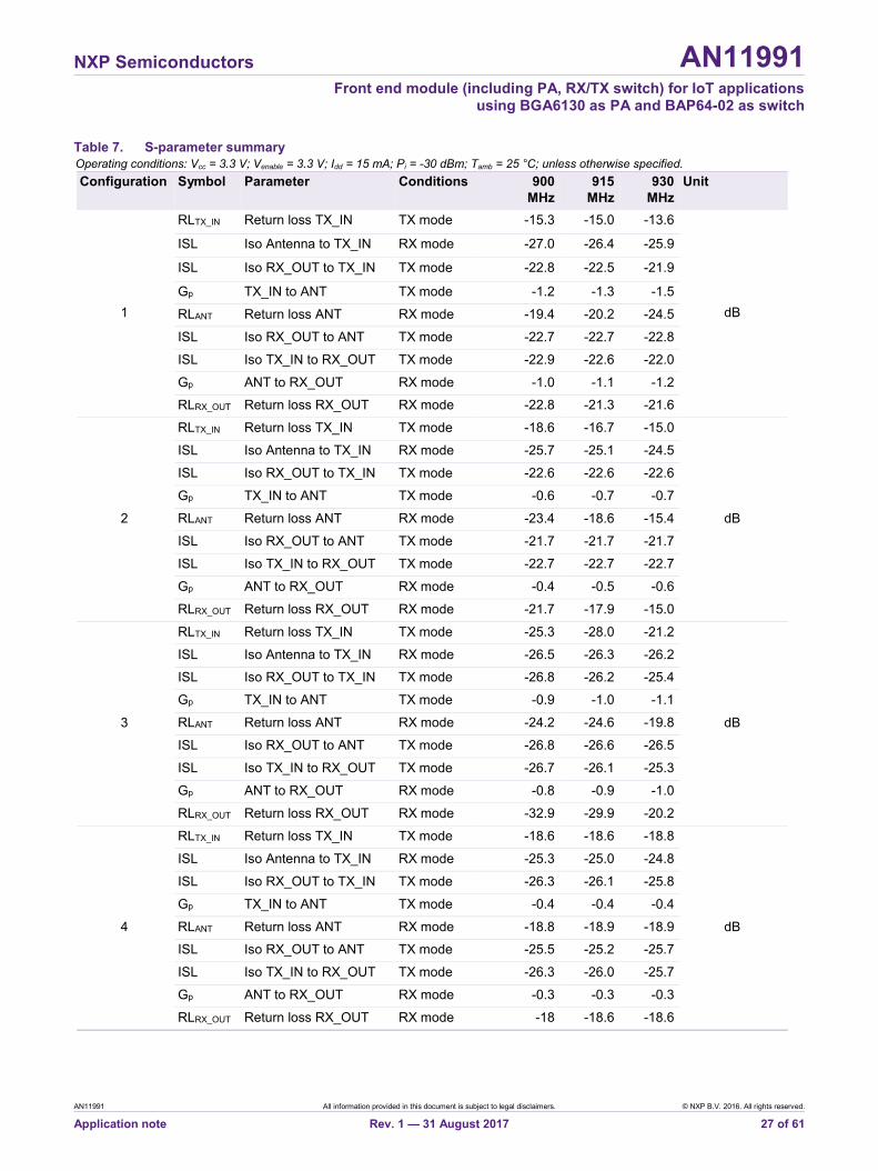
Table 7. S-parameter summary Operating conditions: Vcc = 3.3 V; Venable = 3.3 V; Idd = 15 mA; Pi = -30 dBm; Tamb = 25 °C; unless otherwise specified. Configuration Symbol Parameter Conditions 900
MHz 915
MHz 930
MHz Unit
1
RLTX_IN Return loss TX_IN TX mode -15.3 -15.0 -13.6
dB
ISL Iso Antenna to TX_IN RX mode -27.0 -26.4 -25.9
ISL Iso RX_OUT to TX_IN TX mode -22.8 -22.5 -21.9
Gp TX_IN to ANT TX mode -1.2 -1.3 -1.5
RLANT Return loss ANT RX mode -19.4 -20.2 -24.5
ISL Iso RX_OUT to ANT TX mode -22.7 -22.7 -22.8
ISL Iso TX_IN to RX_OUT TX mode -22.9 -22.6 -22.0
Gp ANT to RX_OUT RX mode -1.0 -1.1 -1.2
RLRX_OUT Return loss RX_OUT RX mode -22.8 -21.3 -21.6
2
RLTX_IN Return loss TX_IN TX mode -18.6 -16.7 -15.0
dB
ISL Iso Antenna to TX_IN RX mode -25.7 -25.1 -24.5
ISL Iso RX_OUT to TX_IN TX mode -22.6 -22.6 -22.6
Gp TX_IN to ANT TX mode -0.6 -0.7 -0.7
RLANT Return loss ANT RX mode -23.4 -18.6 -15.4
ISL Iso RX_OUT to ANT TX mode -21.7 -21.7 -21.7
ISL Iso TX_IN to RX_OUT TX mode -22.7 -22.7 -22.7
Gp ANT to RX_OUT RX mode -0.4 -0.5 -0.6
RLRX_OUT Return loss RX_OUT RX mode -21.7 -17.9 -15.0
3
RLTX_IN Return loss TX_IN TX mode -25.3 -28.0 -21.2
dB
ISL Iso Antenna to TX_IN RX mode -26.5 -26.3 -26.2
ISL Iso RX_OUT to TX_IN TX mode -26.8 -26.2 -25.4
Gp TX_IN to ANT TX mode -0.9 -1.0 -1.1
RLANT Return loss ANT RX mode -24.2 -24.6 -19.8
ISL Iso RX_OUT to ANT TX mode -26.8 -26.6 -26.5
ISL Iso TX_IN to RX_OUT TX mode -26.7 -26.1 -25.3
Gp ANT to RX_OUT RX mode -0.8 -0.9 -1.0
RLRX_OUT Return loss RX_OUT RX mode -32.9 -29.9 -20.2
4
RLTX_IN Return loss TX_IN TX mode -18.6 -18.6 -18.8
dB
ISL Iso Antenna to TX_IN RX mode -25.3 -25.0 -24.8
ISL Iso RX_OUT to TX_IN TX mode -26.3 -26.1 -25.8
Gp TX_IN to ANT TX mode -0.4 -0.4 -0.4
RLANT Return loss ANT RX mode -18.8 -18.9 -18.9
ISL Iso RX_OUT to ANT TX mode -25.5 -25.2 -25.7
ISL Iso TX_IN to RX_OUT TX mode -26.3 -26.0 -25.7
Gp ANT to RX_OUT RX mode -0.3 -0.3 -0.3
RLRX_OUT Return loss RX_OUT RX mode -18 -18.6 -18.6
NXP Semiconductors AN11991
Front end module (including PA, RX/TX switch) for IoT applications using BGA6130 as PA and BAP64-02 as switch
AN11991 All information provided in this document is subject to legal disclaimers. © NXP B.V. 2016. All rights reserved.
Application note Rev. 1 — 31 August 2017 28 of 61
3.5.2 In-band 1dB gain compression The 1 dB compression level determines the power handling capability of the RX/TX switch. This capability is only for interest in the TX mode due to the high power level normally used in the transmit mode.
The 1dB gain compression is determined by applying an RF-power sweep at the input of the TX and measure the output power at the antenna output. The application is first set into the transmit mode before applying the power sweep.
During the P1dB measurement of the application without the BGA6130, no degradation on linearity was observed up to 40 dBm input power.
NXP Semiconductors AN11991
Front end module (including PA, RX/TX switch) for IoT applications using BGA6130 as PA and BAP64-02 as switch
AN11991 All information provided in this document is subject to legal disclaimers. © NXP B.V. 2016. All rights reserved.
Application note Rev. 1 — 31 August 2017 29 of 61
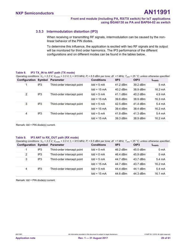
3.5.3 Intermodulation distortion (IP3) When receiving or transmitting RF signals, intermodulation can be caused by the non- linear behavior of the PIN diodes.
To determine this influence, the application is excited with two RF signals and its output will be monitored for third order harmonics. The IP3 performance of the different configurations and on different modes can be found in the tables below.
Table 8. IP3 TX_IN to ANT path (TX mode) Operating conditions: Vcc = 3.3 V; Venable = 3.3 V; fc = 915 MHz; Pi = 6.5 dBm per tone; Δf =1 MHz; Tamb = 25 °C; unless otherwise specified. Configuration Symbol Parameter Conditions IIP3 OIP3 Isupply
1 IP3 Third-order intercept point Idd = 5 mA 41.2 dBm 39.2 dBm 5 mA
Idd = 15 mA 40.2 dBm 38.9 dBm 16.2 mA
2 IP3 Third-order intercept point Idd = 5 mA 41.1 dBm 40.2 dBm 4.9 mA
Idd = 15 mA 39.6 dBm 38.9 dBm 16.3 mA
3 IP3 Third-order intercept point Idd = 5 mA 42.5 dBm 41.4 dBm 5.4 mA
Idd = 15 mA 39.4 dBm 38.4 dBm 16.2 mA
4 IP3 Third-order intercept point Idd = 5 mA 41.8 dBm 41.3 dBm 5.4 mA
Idd = 15 mA 39.3 dBm 38.9 dBm 16.2 mA
Remark: Idd = PIN diode(s) current.
Table 9. IP3 ANT to RX_OUT path (RX mode) Operating conditions: Vcc = 3.3 V; Venable = 3.3 V; fc = 915 MHz; Pi = 6.5 dBm per tone; Δf =1 MHz; Tamb = 25 °C; unless otherwise specified. Configuration Symbol Parameter Conditions IIP3 OIP3 Isupply
1 IP3 Third-order intercept point Idd = 0 mA 46.2 dBm 45.0 dBm 0 mA
2 IP3 Third-order intercept point Idd = 0 mA 46.4 dBm 45.9 dBm 0 mA
3 IP3 Third-order intercept point Idd = 5 mA 44.7 dBm 43.7 dBm 5.4 mA
Idd = 15 mA 44.7 dBm 43.7 dBm 16.2 mA
4 IP3 Third-order intercept point Idd = 5 mA 44.4 dBm 44.1 dBm 5.4 mA
Idd = 15 mA 44.6 dBm 44.3 dBm 16.1 mA
Remark: Idd = PIN diode(s) current.
NXP Semiconductors AN11991
Front end module (including PA, RX/TX switch) for IoT applications using BGA6130 as PA and BAP64-02 as switch
AN11991 All information provided in this document is subject to legal disclaimers. © NXP B.V. 2016. All rights reserved.
Application note Rev. 1 — 31 August 2017 30 of 61
4. RX/TX switch with MPA evaluation board There are two versions of the evaluation board available. The difference of these two versions is an additional medium power amplifier (MPA). This paragraph describes the version with the additional MPA in more detail.
Typical characteristics:
• High output power capability
• High gain
• Zero current during receive mode with MPA disabled (narrow bandwidth version)
• Low component count (depends on customer application)
NXP Semiconductors AN11991
Front end module (including PA, RX/TX switch) for IoT applications using BGA6130 as PA and BAP64-02 as switch
AN11991 All information provided in this document is subject to legal disclaimers. © NXP B.V. 2016. All rights reserved.
Application note Rev. 1 — 31 August 2017 31 of 61
4.1 Summary measurement results
Table 10. Summary measurement results Operating conditions: Vcc = 3.3 V; fc = 915 MHz; Pi = 6.5 dBm per tone; Δf =1 MHz; Tamb = 25 °C; unless otherwise specified.
Configuration Symbol Parameter Conditions Typ. Unit
5
Idd Current consumption RX mode 0.0 mA
TX mode 15.0 mA
Gp Transmission TX_IN to ANT TX mode 11.5 dB
Gp Transmission ANT to RX_OUT RX mode -1.2 dB
ISL Isolation TX_IN to RX_OUT TX mode -9.9 dB
IIP3 Input third-order intercept point TX mode 27.4 dBm
OIP3 Output third-order intercept point TX mode 38.9 dBm
IP1dB Input 1dB compression point TX mode 15.5 dBm
OP1dB Output 1dB compression point TX mode 26.2 dBm
6
Idd Current consumption RX mode 0.0 mA
TX mode 15.0 mA
Gp Transmission TX_IN to ANT TX mode 12.8 dB
Gp Transmission ANT to RX_OUT RX mode -0.5 dB
ISL Isolation TX_IN to RX_OUT TX mode -9.2 dB
IIP3 Input third-order intercept point TX mode 26.1 dBm
OIP3 Output third-order intercept point TX mode 38.9 dBm
IP1dB Input 1dB compression point TX mode 15.3 dBm
OP1dB Output 1dB compression point TX mode 27.1 dBm
7
Idd Current consumption RX mode 15.0 mA
TX mode 15.0 mA
Gp Transmission TX_IN to ANT TX mode 11.8 dB
Gp Transmission ANT to RX_OUT RX mode -1.0 dB
ISL Isolation TX_IN to RX_OUT TX mode -13.7 dB
IIP3 Input third-order intercept point TX mode 26.6 dBm
OIP3 Output third-order intercept point TX mode 38.4 dBm
IP1dB Input 1dB compression point TX mode 15.3 dBm
OP1dB Output 1dB compression point TX mode 26.3 dBm
8
Idd Current consumption RX mode 15.0 mA
TX mode 15.0 mA
Gp Transmission TX_IN to ANT TX mode 13.1 dB
Gp Transmission ANT to RX_OUT RX mode -0.3 dB
ISL Isolation TX_IN to RX_OUT TX mode -12.9 dB
IIP3 Input third-order intercept point TX mode 25.8 dBm
OIP3 Output third-order intercept point TX mode 38.9 dBm
IP1dB Input 1dB compression point TX mode 14.8 dBm
NXP Semiconductors AN11991
Front end module (including PA, RX/TX switch) for IoT applications using BGA6130 as PA and BAP64-02 as switch
AN11991 All information provided in this document is subject to legal disclaimers. © NXP B.V. 2016. All rights reserved.
Application note Rev. 1 — 31 August 2017 32 of 61
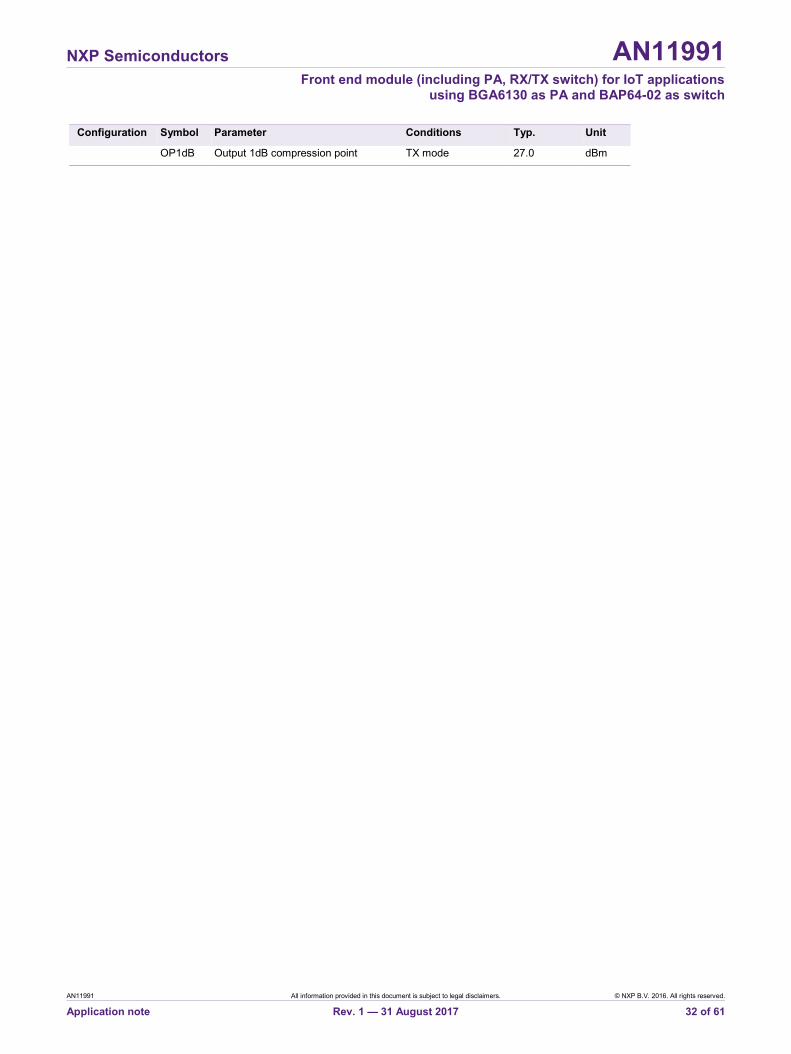
Configuration Symbol Parameter Conditions Typ. Unit
OP1dB Output 1dB compression point TX mode 27.0 dBm
NXP Semiconductors AN11991
Front end module (including PA, RX/TX switch) for IoT applications using BGA6130 as PA and BAP64-02 as switch
AN11991 All information provided in this document is subject to legal disclaimers. © NXP B.V. 2016. All rights reserved.
Application note Rev. 1 — 31 August 2017 33 of 61
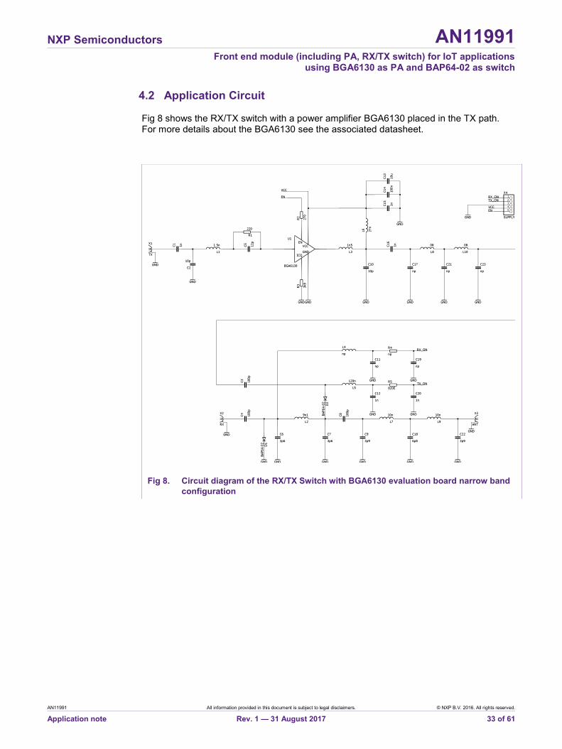
4.2 Application Circuit Fig 8 shows the RX/TX switch with a power amplifier BGA6130 placed in the TX path. For more details about the BGA6130 see the associated datasheet.
Fig 8. Circuit diagram of the RX/TX Switch with BGA6130 evaluation board narrow band configuration
NXP Semiconductors AN11991
Front end module (including PA, RX/TX switch) for IoT applications using BGA6130 as PA and BAP64-02 as switch
AN11991 All information provided in this document is subject to legal disclaimers. © NXP B.V. 2016. All rights reserved.
Application note Rev. 1 — 31 August 2017 34 of 61
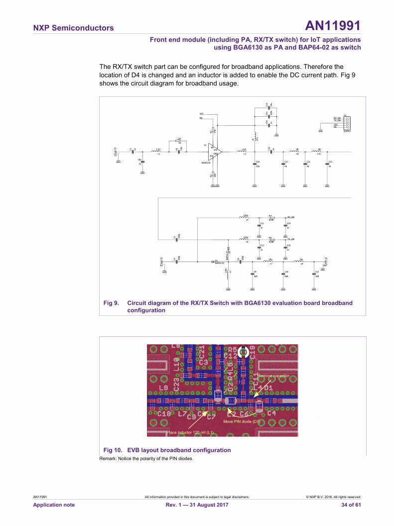
The RX/TX switch part can be configured for broadband applications. Therefore the location of D4 is changed and an inductor is added to enable the DC current path. Fig 9 shows the circuit diagram for broadband usage.
Remark: Notice the polarity of the PIN diodes.
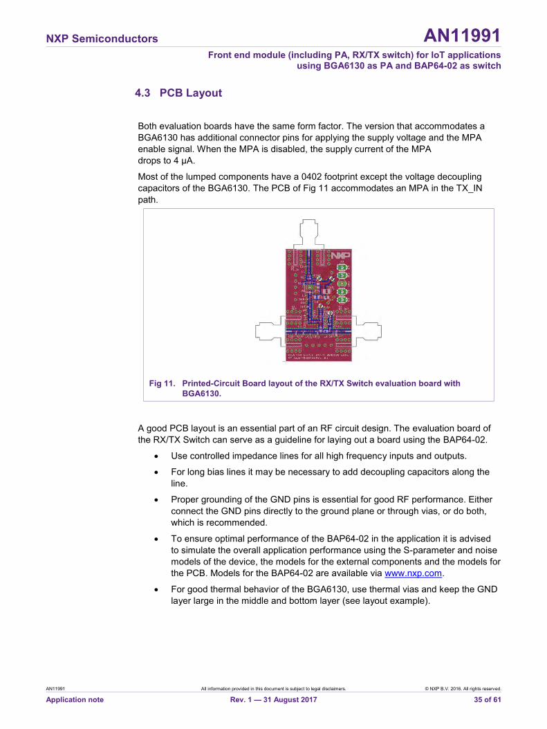
Fig 9. Circuit diagram of the RX/TX Switch with BGA6130 evaluation board broadband configuration
Fig 10. EVB layout broadband configuration
Place inductor 120 nH (L1)
Move PIN diode (D1)
Remove capacitor
NXP Semiconductors AN11991
Front end module (including PA, RX/TX switch) for IoT applications using BGA6130 as PA and BAP64-02 as switch
AN11991 All information provided in this document is subject to legal disclaimers. © NXP B.V. 2016. All rights reserved.
Application note Rev. 1 — 31 August 2017 35 of 61
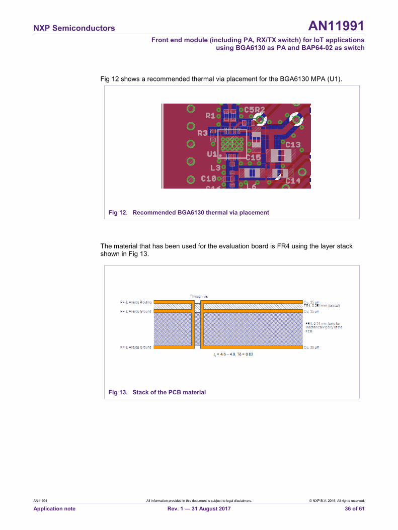
4.3 PCB Layout
Both evaluation boards have the same form factor. The version that accommodates a BGA6130 has additional connector pins for applying the supply voltage and the MPA enable signal. When the MPA is disabled, the supply current of the MPA drops to 4 µA.
Most of the lumped components have a 0402 footprint except the voltage decoupling capacitors of the BGA6130. The PCB of Fig 11 accommodates an MPA in the TX_IN path.
Fig 11. Printed-Circuit Board layout of the RX/TX Switch evaluation board with BGA6130.
A good PCB layout is an essential part of an RF circuit design. The evaluation board of the RX/TX Switch can serve as a guideline for laying out a board using the BAP64-02.
• Use controlled impedance lines for all high frequency inputs and outputs.
• For long bias lines it may be necessary to add decoupling capacitors along the line.
• Proper grounding of the GND pins is essential for good RF performance. Either connect the GND pins directly to the ground plane or through vias, or do both, which is recommended.
• To ensure optimal performance of the BAP64-02 in the application it is advised to simulate the overall application performance using the S-parameter and noise models of the device, the models for the external components and the models for the PCB. Models for the BAP64-02 are available via www.nxp.com.
• For good thermal behavior of the BGA6130, use thermal vias and keep the GND layer large in the middle and bottom layer (see layout example).
NXP Semiconductors AN11991
Front end module (including PA, RX/TX switch) for IoT applications using BGA6130 as PA and BAP64-02 as switch
AN11991 All information provided in this document is subject to legal disclaimers. © NXP B.V. 2016. All rights reserved.
Application note Rev. 1 — 31 August 2017 36 of 61
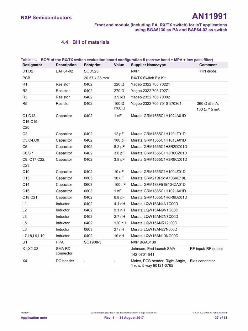
Fig 12 shows a recommended thermal via placement for the BGA6130 MPA (U1).
Fig 12. Recommended BGA6130 thermal via placement
The material that has been used for the evaluation board is FR4 using the layer stack shown in Fig 13.
Fig 13. Stack of the PCB material
NXP Semiconductors AN11991
Front end module (including PA, RX/TX switch) for IoT applications using BGA6130 as PA and BAP64-02 as switch
AN11991 All information provided in this document is subject to legal disclaimers. © NXP B.V. 2016. All rights reserved.
Application note Rev. 1 — 31 August 2017 37 of 61
4.4 Bill of materials
Table 11. BOM of the RX/TX switch evaluation board configuration 5 (narrow band + MPA + low pass filter) Designator Description Footprint Value Supplier Name/type Comment D1,D2 BAP64-02 SOD523 NXP PIN diode
PCB 20.57 x 35 mm RX/TX Switch EV Kit
R1 Resistor 0402 220 Ω Yageo 2322 705 70221
R2 Resistor 0402 270 Ω Yageo 2322 705 70271
R3 Resistor 0402 3.9 kΩ Yageo 2322 705 70392
R5 Resistor 0402 100 Ω /360 Ω
Yageo 2322 705 70101/70361 360 Ω /5 mA, 100 Ω /15 mA
C1,C12, C16,C19, C20
Capacitor 0402 1 nF Murata GRM1555C1H102JA01D
C2 Capacitor 0402 12 pF Murata GRM1555C1H120JZ01D
C3,C4,C8 Capacitor 0402 180 pF Murata GRM1555C1H181JA01D
C5 Capacitor 0402 8.2 pF Murata GRM1555C1H8R2DZ01D
C6,C7 Capacitor 0402 3.6 pF Murata GRM1555C1H3R6CZ01D
C9, C17,C22, C23
Capacitor 0402 3.9 pF Murata GRM1555C1H3R9CZ01D
C10 Capacitor 0402 10 uF Murata GRM1555C1H100JZ01D
C13 Capacitor 0805 10 uF Murata GRM21BR61A106KE19L
C14 Capacitor 0603 100 nF Murata GRM188F51E104ZA01D
C15 Capacitor 0603 1 nF Murata GRM1885C1H102JA01D
C18,C21 Capacitor 0402 6.8 pF Murata GRM1555C1H6R8DZ01D
L1 Inductor 0402 4.1 nH Murata LQW15AN4N1C00D
L2 Inductor 0402 9.1 nH Murata LQW15AN9N1G00D
L3 Inductor 0402 2.7 nH Murata LQW15AN2N7C00D
L5 Inductor 0402 120 nH Murata LQW15ANR12J00D
L6 Inductor 0603 27 nH Murata LQW18AN27NJ00D
L7,L8,L9,L10 Inductor 0402 10 nH Murata LQW15AN10NG00D
U1 HPA SOT908-3 NXP BGA6130
X1,X2,X3 SMA RD connector
- - Johnson, End launch SMA 142-0701-841
RF input/ RF output
X4 DC header - - Molex, PCB header, Right Angle, 1 row, 5 way 90121-0765
Bias connector
NXP Semiconductors AN11991
Front end module (including PA, RX/TX switch) for IoT applications using BGA6130 as PA and BAP64-02 as switch
AN11991 All information provided in this document is subject to legal disclaimers. © NXP B.V. 2016. All rights reserved.
Application note Rev. 1 — 31 August 2017 38 of 61
Table 12. BOM of the RX/TX switch evaluation board configuration 6 (narrow band + MPA) Designator Description Footprint Value Supplier Name/type Comment D1,D2 BAP64-02 SOD523 NXP PIN diode
PCB 20.57 x 35 mm RX/TX Switch EV Kit
R1 Resistor 0402 220 Ω Yageo 2322 705 70221
R2 Resistor 0402 270 Ω Yageo 2322 705 70271
R3 Resistor 0402 3.9 kΩ Yageo 2322 705 70392
R5 Resistor 0402 100 Ω /360 Ω
Yageo 2322 705 70101/70361 360 Ω /5 mA, 100 Ω /15 mA
C1,C12, C16,C19, C20
Capacitor 0402 1 nF Murata GRM1555C1H102JA01D
C2 Capacitor 0402 12 pF Murata GRM1555C1H120JZ01D
C3,C4,C8 Capacitor 0402 180 pF Murata GRM1555C1H181JA01D
C5 Capacitor 0402 8.2 pF Murata GRM1555C1H8R2DZ01D
C6,C7 Capacitor 0402 3.6 pF Murata GRM1555C1H3R6CZ01D
C10 Capacitor 0402 10 pF Murata GRM1555C1H100JZ01D
C13 Capacitor 0805 10 uF Murata GRM21BR61A106KE19L
C14 Capacitor 0603 100 nF Murata GRM188F51E104ZA01D
C15 Capacitor 0603 1 nF Murata GRM1885C1H102JA01D
L1 Inductor 0402 4.1 nH Murata LQW15AN4N1C00D
L2 Inductor 0402 9.1 nH Murata LQW15AN9N1G00D
L3 Inductor 0402 2.7 nH Murata LQW15AN2N7C00D
L5 Inductor 0402 120 nH Murata LQW15ANR12J00D
L6 Inductor 0603 27 nH Murata LQW18AN27NJ00D
L7,L8,L9,L10 Resistor 0402 0 Ω Yageo 2322 705 91001 Jumper
U1 HPA SOT908-3 NXP BGA6130
X1,X2,X3 SMA RD connector
- - Johnson, End launch SMA 142-0701-841
RF input/ RF output
X4 DC header - - Molex, PCB header, Right Angle, 1 row, 5 way 90121-0765
Bias connector
NXP Semiconductors AN11991
Front end module (including PA, RX/TX switch) for IoT applications using BGA6130 as PA and BAP64-02 as switch
AN11991 All information provided in this document is subject to legal disclaimers. © NXP B.V. 2016. All rights reserved.
Application note Rev. 1 — 31 August 2017 39 of 61
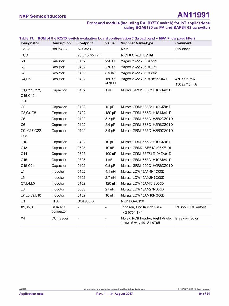
Table 13. BOM of the RX/TX switch evaluation board configuration 7 (broad band + MPA + low pass filter) Designator Description Footprint Value Supplier Name/type Comment L2,D2 BAP64-02 SOD523 NXP PIN diode
PCB 20.57 x 35 mm RX/TX Switch EV Kit
R1 Resistor 0402 220 Ω Yageo 2322 705 70221
R2 Resistor 0402 270 Ω Yageo 2322 705 70271
R3 Resistor 0402 3.9 kΩ Yageo 2322 705 70392
R4,R5 Resistor 0402 150 Ω /470 Ω
Yageo 2322 705 70151/70471 470 Ω /5 mA, 150 Ω /15 mA
C1,C11,C12, C16,C19, C20
Capacitor 0402 1 nF Murata GRM1555C1H102JA01D
C2 Capacitor 0402 12 pF Murata GRM1555C1H120JZ01D
C3,C4,C8 Capacitor 0402 180 pF Murata GRM1555C1H181JA01D
C5 Capacitor 0402 8.2 pF Murata GRM1555C1H8R2DZ01D
C6 Capacitor 0402 3.6 pF Murata GRM1555C1H3R6CZ01D
C9, C17,C22, C23
Capacitor 0402 3.9 pF Murata GRM1555C1H3R9CZ01D
C10 Capacitor 0402 10 pF Murata GRM1555C1H100JZ01D
C13 Capacitor 0805 10 uF Murata GRM21BR61A106KE19L
C14 Capacitor 0603 100 nF Murata GRM188F51E104ZA01D
C15 Capacitor 0603 1 nF Murata GRM1885C1H102JA01D
C18,C21 Capacitor 0402 6.8 pF Murata GRM1555C1H6R8DZ01D
L1 Inductor 0402 4.1 nH Murata LQW15AN4N1C00D
L3 Inductor 0402 2.7 nH Murata LQW15AN2N7C00D
C7,L4,L5 Inductor 0402 120 nH Murata LQW15ANR12J00D
L6 Inductor 0603 27 nH Murata LQW18AN27NJ00D
L7,L8,L9,L10 Inductor 0402 10 nH Murata LQW15AN10NG00D
U1 HPA SOT908-3 NXP BGA6130
X1,X2,X3 SMA RD connector
- - Johnson, End launch SMA 142-0701-841
RF input/ RF output
X4 DC header - - Molex, PCB header, Right Angle, 1 row, 5 way 90121-0765
Bias connector
NXP Semiconductors AN11991
Front end module (including PA, RX/TX switch) for IoT applications using BGA6130 as PA and BAP64-02 as switch
AN11991 All information provided in this document is subject to legal disclaimers. © NXP B.V. 2016. All rights reserved.
Application note Rev. 1 — 31 August 2017 40 of 61
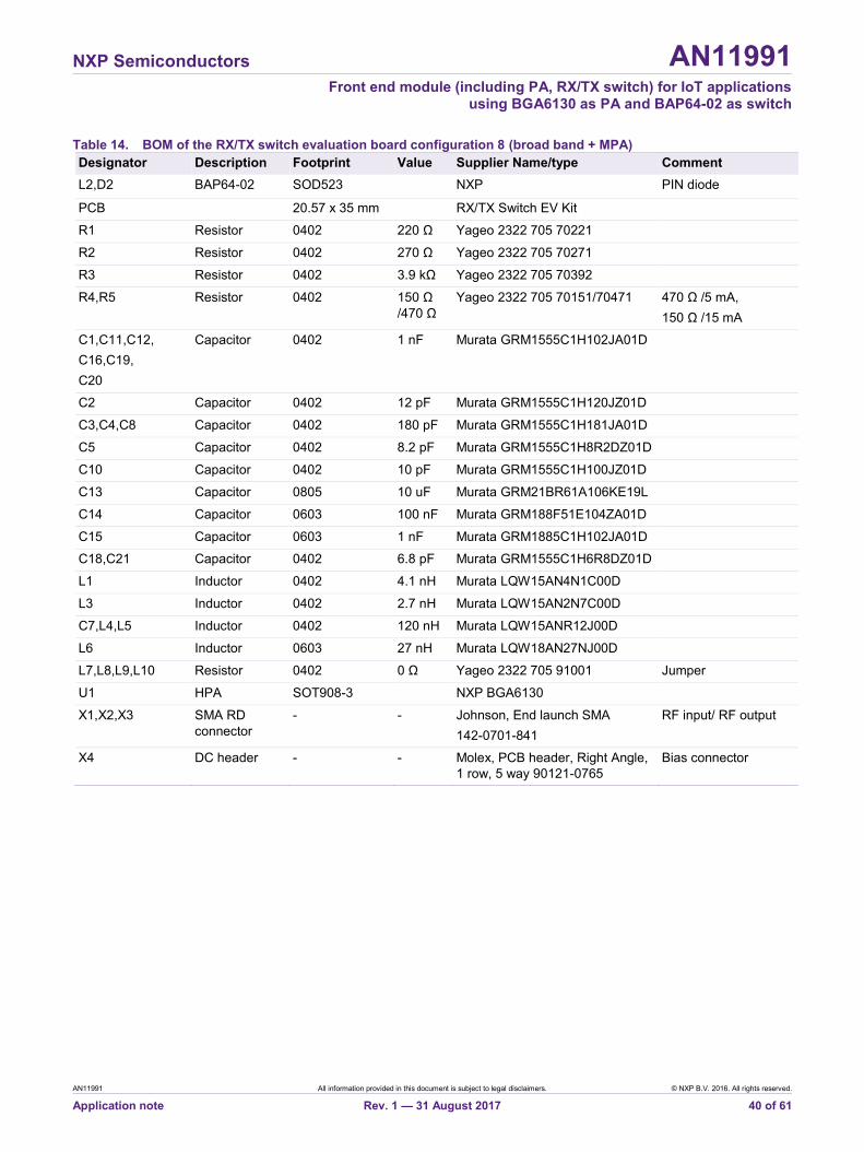
Table 14. BOM of the RX/TX switch evaluation board configuration 8 (broad band + MPA) Designator Description Footprint Value Supplier Name/type Comment L2,D2 BAP64-02 SOD523 NXP PIN diode
PCB 20.57 x 35 mm RX/TX Switch EV Kit
R1 Resistor 0402 220 Ω Yageo 2322 705 70221
R2 Resistor 0402 270 Ω Yageo 2322 705 70271
R3 Resistor 0402 3.9 kΩ Yageo 2322 705 70392
R4,R5 Resistor 0402 150 Ω /470 Ω
Yageo 2322 705 70151/70471 470 Ω /5 mA, 150 Ω /15 mA
C1,C11,C12, C16,C19, C20
Capacitor 0402 1 nF Murata GRM1555C1H102JA01D
C2 Capacitor 0402 12 pF Murata GRM1555C1H120JZ01D
C3,C4,C8 Capacitor 0402 180 pF Murata GRM1555C1H181JA01D
C5 Capacitor 0402 8.2 pF Murata GRM1555C1H8R2DZ01D
C10 Capacitor 0402 10 pF Murata GRM1555C1H100JZ01D
C13 Capacitor 0805 10 uF Murata GRM21BR61A106KE19L
C14 Capacitor 0603 100 nF Murata GRM188F51E104ZA01D
C15 Capacitor 0603 1 nF Murata GRM1885C1H102JA01D
C18,C21 Capacitor 0402 6.8 pF Murata GRM1555C1H6R8DZ01D
L1 Inductor 0402 4.1 nH Murata LQW15AN4N1C00D
L3 Inductor 0402 2.7 nH Murata LQW15AN2N7C00D
C7,L4,L5 Inductor 0402 120 nH Murata LQW15ANR12J00D
L6 Inductor 0603 27 nH Murata LQW18AN27NJ00D
L7,L8,L9,L10 Resistor 0402 0 Ω Yageo 2322 705 91001 Jumper
U1 HPA SOT908-3 NXP BGA6130
X1,X2,X3 SMA RD connector
- - Johnson, End launch SMA 142-0701-841
RF input/ RF output
X4 DC header - - Molex, PCB header, Right Angle, 1 row, 5 way 90121-0765
Bias connector
NXP Semiconductors AN11991
Front end module (including PA, RX/TX switch) for IoT applications using BGA6130 as PA and BAP64-02 as switch
AN11991 All information provided in this document is subject to legal disclaimers. © NXP B.V. 2016. All rights reserved.
Application note Rev. 1 — 31 August 2017 41 of 61
4.5 Measurement results The measurements are performed at a supply voltage of Vcc=3.3 V at an ambient temperature of 25 °C unless stated otherwise.
4.5.1 S-parameters (3-port) Because the RX/TX switch contains three RF-ports, it is desirable to have a three ports small signal S-parameter measurement. There are two situations to be analyzed. The RX/TX switch can be set in RX or TX mode. For both situations an S-parameter measurement is performed. The measurements are performed under the following conditions:
- Pin = -30 dBm
- Frequency = 10 – 6000 MHz
- Ambient temperature = 25 °C
In the TX mode, the RX_OUT port is isolated from the TX_IN and ANT port.
Next graphs shows the S-parameters measured at different PIN diode currents (Idd). The graphs also shows the low-pass filter response. It has a cut-off frequency of approximately 1 GHz.
NXP Semiconductors AN11991
Front end module (including PA, RX/TX switch) for IoT applications using BGA6130 as PA and BAP64-02 as switch
AN11991 All information provided in this document is subject to legal disclaimers. © NXP B.V. 2016. All rights reserved.
Application note Rev. 1 — 31 August 2017 42 of 61
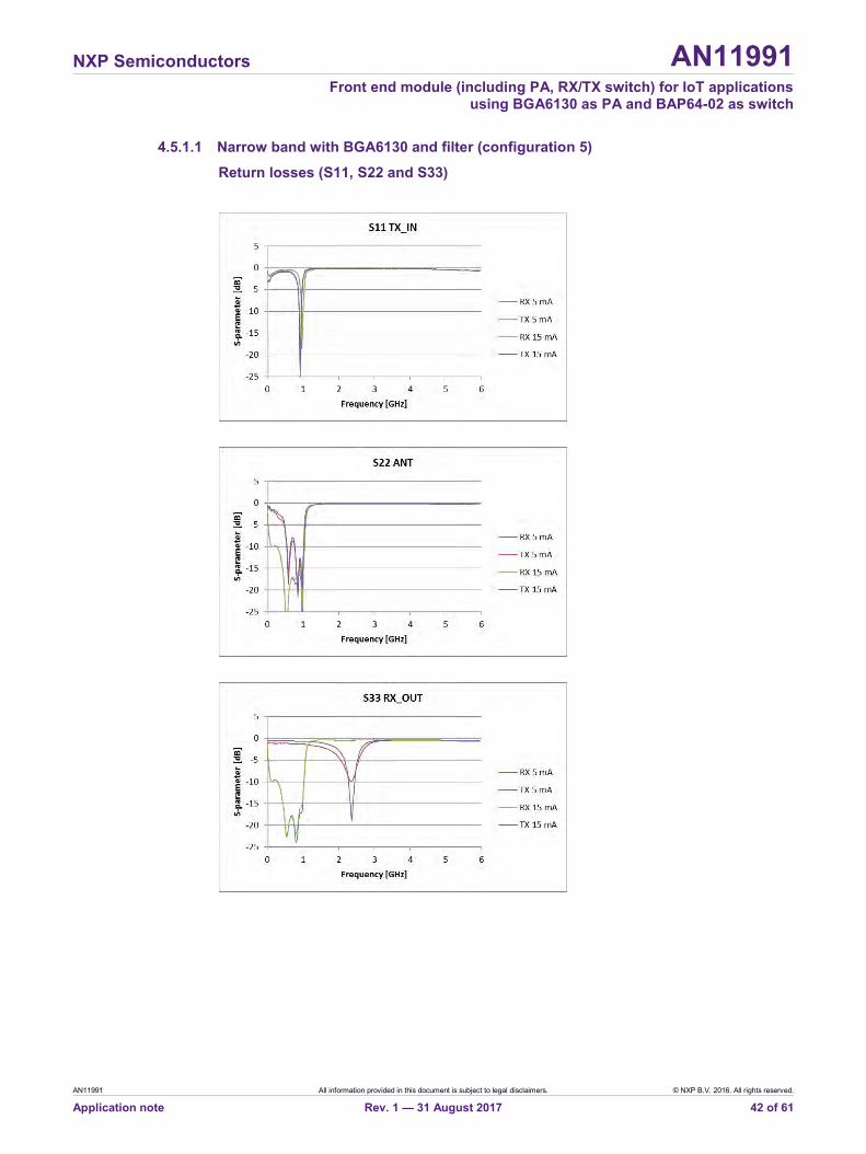
4.5.1.1 Narrow band with BGA6130 and filter (configuration 5)
Return losses (S11, S22 and S33)
NXP Semiconductors AN11991
Front end module (including PA, RX/TX switch) for IoT applications using BGA6130 as PA and BAP64-02 as switch
AN11991 All information provided in this document is subject to legal disclaimers. © NXP B.V. 2016. All rights reserved.
Application note Rev. 1 — 31 August 2017 43 of 61
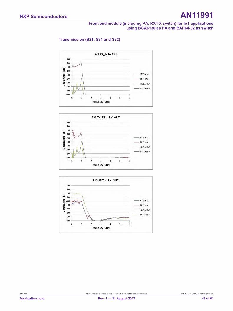
Transmission (S21, S31 and S32)
NXP Semiconductors AN11991
Front end module (including PA, RX/TX switch) for IoT applications using BGA6130 as PA and BAP64-02 as switch
AN11991 All information provided in this document is subject to legal disclaimers. © NXP B.V. 2016. All rights reserved.
Application note Rev. 1 — 31 August 2017 44 of 61
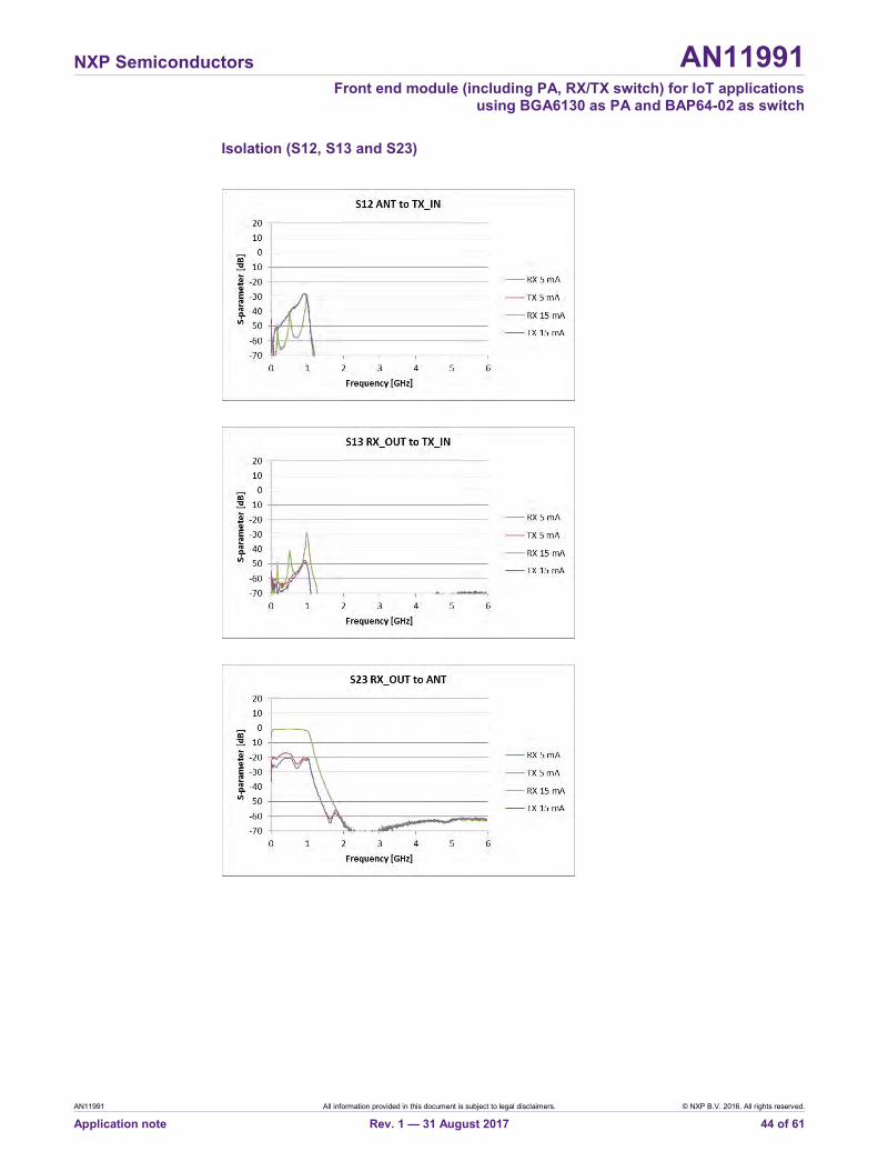
Isolation (S12, S13 and S23)
NXP Semiconductors AN11991
Front end module (including PA, RX/TX switch) for IoT applications using BGA6130 as PA and BAP64-02 as switch
AN11991 All information provided in this document is subject to legal disclaimers. © NXP B.V. 2016. All rights reserved.
Application note Rev. 1 — 31 August 2017 45 of 61
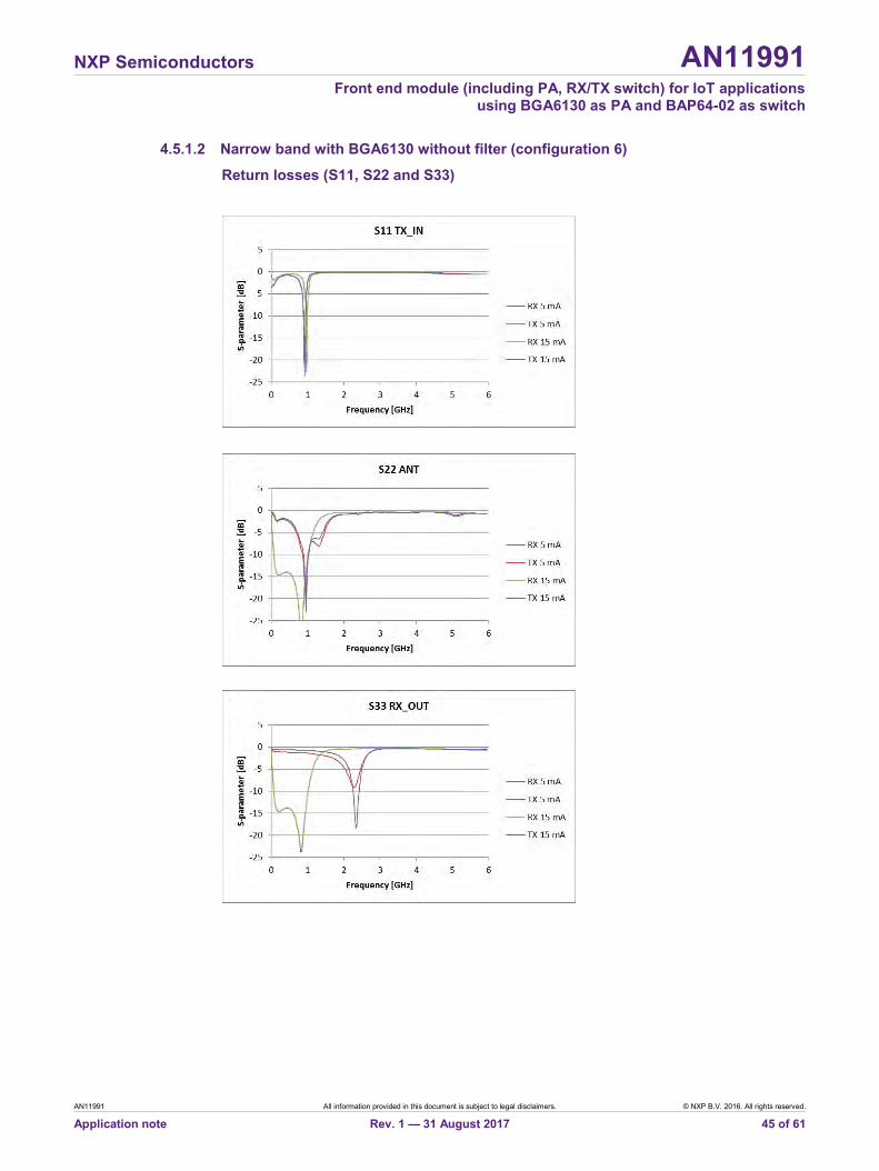
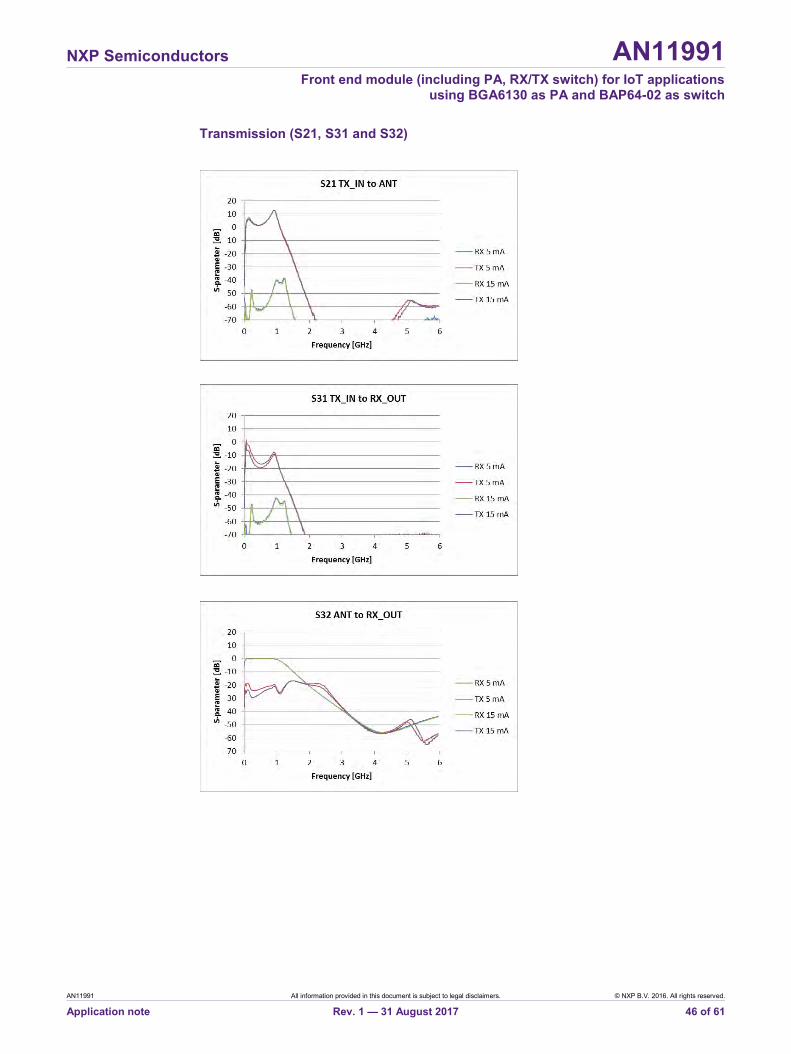
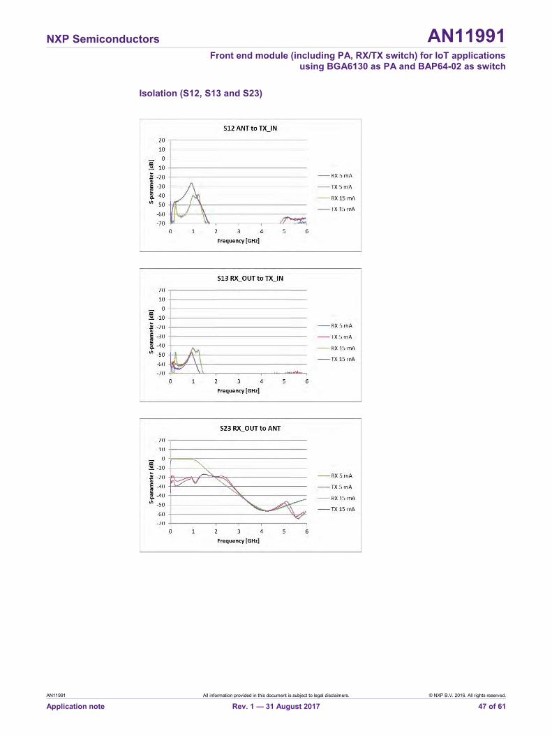
4.5.1.2 Narrow band with BGA6130 without filter (configuration 6)
Return losses (S11, S22 and S33)
NXP Semiconductors AN11991
Front end module (including PA, RX/TX switch) for IoT applications using BGA6130 as PA and BAP64-02 as switch
AN11991 All information provided in this document is subject to legal disclaimers. © NXP B.V. 2016. All rights reserved.
Application note Rev. 1 — 31 August 2017 46 of 61
Transmission (S21, S31 and S32)
NXP Semiconductors AN11991
Front end module (including PA, RX/TX switch) for IoT applications using BGA6130 as PA and BAP64-02 as switch
AN11991 All information provided in this document is subject to legal disclaimers. © NXP B.V. 2016. All rights reserved.
Application note Rev. 1 — 31 August 2017 47 of 61
Isolation (S12, S13 and S23)
NXP Semiconductors AN11991
Front end module (including PA, RX/TX switch) for IoT applications using BGA6130 as PA and BAP64-02 as switch
AN11991 All information provided in this document is subject to legal disclaimers. © NXP B.V. 2016. All rights reserved.
Application note Rev. 1 — 31 August 2017 48 of 61
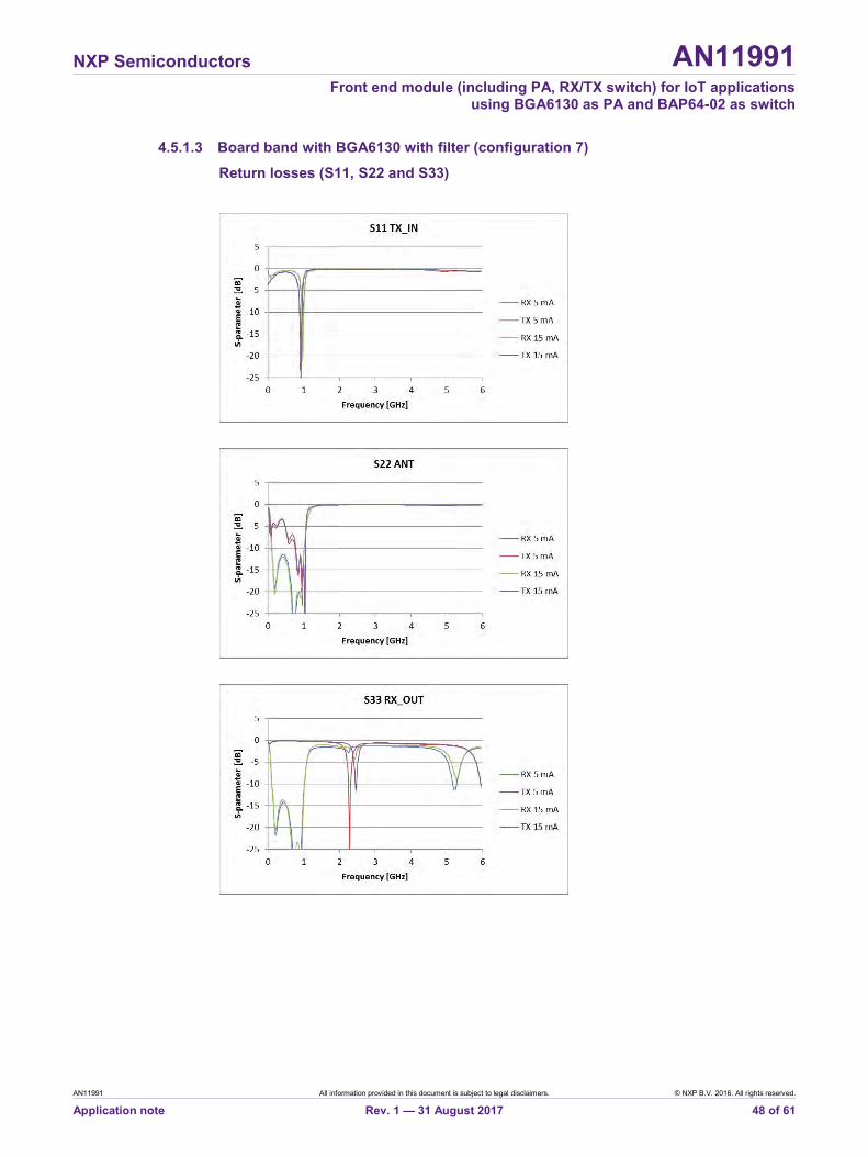
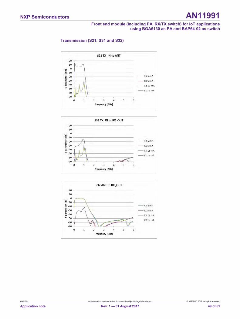
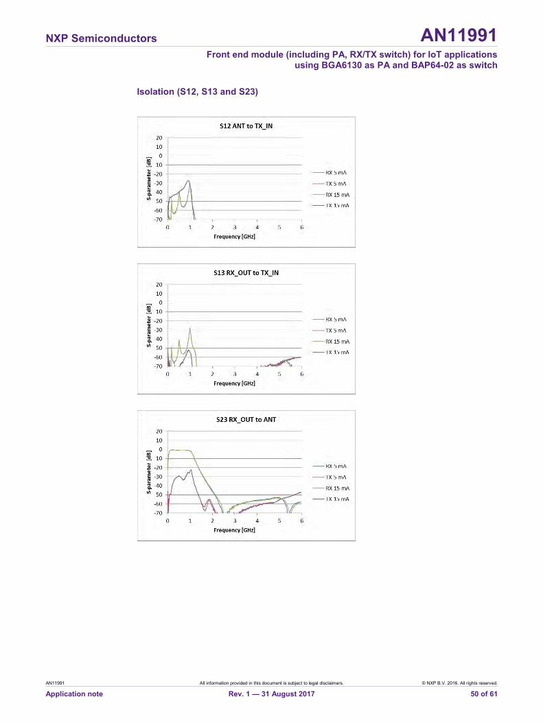
4.5.1.3 Board band with BGA6130 with filter (configuration 7)
Return losses (S11, S22 and S33)
NXP Semiconductors AN11991
Front end module (including PA, RX/TX switch) for IoT applications using BGA6130 as PA and BAP64-02 as switch
AN11991 All information provided in this document is subject to legal disclaimers. © NXP B.V. 2016. All rights reserved.
Application note Rev. 1 — 31 August 2017 49 of 61
Transmission (S21, S31 and S32)
NXP Semiconductors AN11991
Front end module (including PA, RX/TX switch) for IoT applications using BGA6130 as PA and BAP64-02 as switch
AN11991 All information provided in this document is subject to legal disclaimers. © NXP B.V. 2016. All rights reserved.
Application note Rev. 1 — 31 August 2017 50 of 61
Isolation (S12, S13 and S23)
NXP Semiconductors AN11991
Front end module (including PA, RX/TX switch) for IoT applications using BGA6130 as PA and BAP64-02 as switch
AN11991 All information provided in this document is subject to legal disclaimers. © NXP B.V. 2016. All rights reserved.
Application note Rev. 1 — 31 August 2017 51 of 61
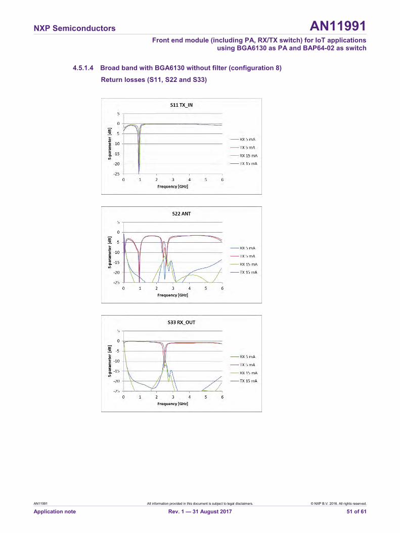
4.5.1.4 Broad band with BGA6130 without filter (configuration 8)
Return losses (S11, S22 and S33)
NXP Semiconductors AN11991
Front end module (including PA, RX/TX switch) for IoT applications using BGA6130 as PA and BAP64-02 as switch
AN11991 All information provided in this document is subject to legal disclaimers. © NXP B.V. 2016. All rights reserved.
Application note Rev. 1 — 31 August 2017 52 of 61
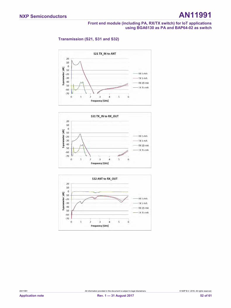
Transmission (S21, S31 and S32)
NXP Semiconductors AN11991
Front end module (including PA, RX/TX switch) for IoT applications using BGA6130 as PA and BAP64-02 as switch
AN11991 All information provided in this document is subject to legal disclaimers. © NXP B.V. 2016. All rights reserved.
Application note Rev. 1 — 31 August 2017 53 of 61
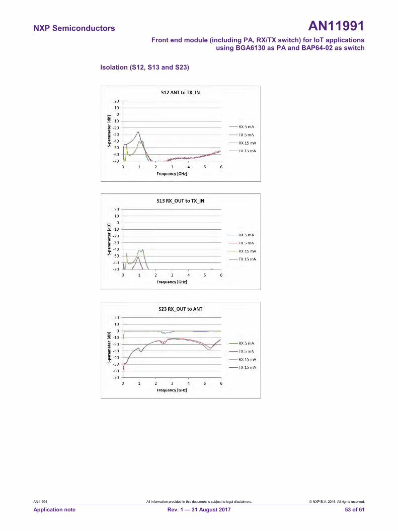
Isolation (S12, S13 and S23)

NXP Semiconductors AN11991
Front end module (including PA, RX/TX switch) for IoT applications using BGA6130 as PA and BAP64-02 as switch
AN11991 All information provided in this document is subject to legal disclaimers. © NXP B.V. 2016. All rights reserved.
Application note Rev. 1 — 31 August 2017 54 of 61
Table 15. S-parameter summary Operating conditions: Vcc = 3.3 V; Venable = 3.3 V; Idd = 15 mA; IQMPA = 70 mA; Pi = -30 dBm; Tamb = 25 °C; unless otherwise specified. Configuration Symbol Parameter Conditions 900
MHz 915
MHz 930
MHz Unit
5
RLTX_IN Return loss TX_IN TX mode -9.8 -25.2 -9.3
dB
ISL Iso Antenna to TX_IN RX mode -46.3 -41.6 -35.6
ISL Iso RX_OUT to TX_IN TX mode -49.6 -48.9 -48.9
Gp TX_IN to ANT TX mode 11.4 11.5 10.4
RLANT Return loss ANT RX mode -15.3 -15.7 -18.1
ISL Iso RX_OUT to ANT TX mode -21.4 -21.2 -21.9
ISL Iso TX_IN to RX_OUT TX mode -10.4 -9.9 -10.3
Gp ANT to RX_OUT RX mode -1.0 -1.2 -1.3
RLRX_OUT Return loss RX_OUT RX mode -16.9 -15.9 -15.6
6
RLTX_IN Return loss TX_IN TX mode -10.3 -23.6 -7.7
dB
ISL Iso Antenna to TX_IN RX mode -47.2 -44.6 -42.0
ISL Iso RX_OUT to TX_IN TX mode -49.0 -48.2 -48.8
Gp TX_IN to ANT TX mode 12.4 12.8 11.9
RLANT Return loss ANT RX mode -20.1 -16.6 -14.0
ISL Iso RX_OUT to ANT TX mode -21.4 -21.0 -21.5
ISL Iso TX_IN to RX_OUT TX mode -9.7 -9.2 -10.0
Gp ANT to RX_OUT RX mode -0.4 -0.5 -0.6
RLRX_OUT Return loss RX_OUT RX mode -18.4 -15.8 -13.5
7
RLTX_IN Return loss TX_IN TX mode -10.4 -28.3 -8.0
dB
ISL Iso Antenna to TX_IN RX mode -46.4 -42.2 -36.7
ISL Iso RX_OUT to TX_IN TX mode -53.9 -52.8 -52.8
Gp TX_IN to ANT TX mode 11.7 11.8 10.7
RLANT Return loss ANT RX mode -20.8 -21.8 -19.6
ISL Iso RX_OUT to ANT TX mode -25.9 -25.4 -25.7
ISL Iso TX_IN to RX_OUT TX mode -14.5 -13.7 -13.8
Gp ANT to RX_OUT RX mode -0.9 -1.0 -1.1
RLRX_OUT Return loss RX_OUT RX mode -29.6 -37.4 -22.1
8
RLTX_IN Return loss TX_IN TX mode -9.4 -27.8 -8.5
dB
ISL Iso Antenna to TX_IN RX mode -47.3 -44.8 -42.5
ISL Iso RX_OUT to TX_IN TX mode -53.2 -52.0 -52.0
Gp TX_IN to ANT TX mode 12.6 13.1 12.3
RLANT Return loss ANT RX mode -29.9 -30.6 -31.2
ISL Iso RX_OUT to ANT TX mode -26.2 -25.6 -25.7
ISL Iso TX_IN to RX_OUT TX mode -13.8 -12.9 -13.4
Gp ANT to RX_OUT RX mode -0.3 -0.3 -0.3
RLRX_OUT Return loss RX_OUT RX mode -28.6 -29.1 -29.5
NXP Semiconductors AN11991
Front end module (including PA, RX/TX switch) for IoT applications using BGA6130 as PA and BAP64-02 as switch
AN11991 All information provided in this document is subject to legal disclaimers. © NXP B.V. 2016. All rights reserved.
Application note Rev. 1 — 31 August 2017 55 of 61
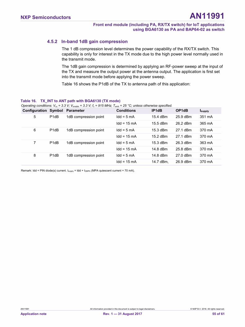
4.5.2 In-band 1dB gain compression The 1 dB compression level determines the power capability of the RX/TX switch. This capability is only for interest in the TX mode due to the high power level normally used in the transmit mode.
The 1dB gain compression is determined by applying an RF-power sweep at the input of the TX and measure the output power at the antenna output. The application is first set into the transmit mode before applying the power sweep.
Table 16 shows the P1dB of the TX to antenna path of this application:
Table 16. TX_INT to ANT path with BGA6130 (TX mode) Operating conditions: Vcc = 3.3 V; Venable = 3.3 V; fc = 915 MHz; Tamb = 25 °C; unless otherwise specified. Configuration Symbol Parameter Conditions IP1dB OP1dB Isupply
5 P1dB 1dB compression point Idd = 5 mA 15.4 dBm 25.9 dBm 351 mA
Idd = 15 mA 15.5 dBm 26.2 dBm 365 mA
6 P1dB 1dB compression point Idd = 5 mA 15.3 dBm 27.1 dBm 370 mA
Idd = 15 mA 15.2 dBm 27.1 dBm 370 mA
7 P1dB 1dB compression point Idd = 5 mA 15.3 dBm 26.3 dBm 363 mA
Idd = 15 mA 14.8 dBm 25.8 dBm 370 mA
8 P1dB 1dB compression point Idd = 5 mA 14.8 dBm 27.0 dBm 370 mA
Idd = 15 mA 14.7 dBm, 26.9 dBm 370 mA
Remark: Idd = PIN diode(s) current. Isupply = Idd + IQMPA (MPA quiescent current = 70 mA).
NXP Semiconductors AN11991
Front end module (including PA, RX/TX switch) for IoT applications using BGA6130 as PA and BAP64-02 as switch
AN11991 All information provided in this document is subject to legal disclaimers. © NXP B.V. 2016. All rights reserved.
Application note Rev. 1 — 31 August 2017 56 of 61
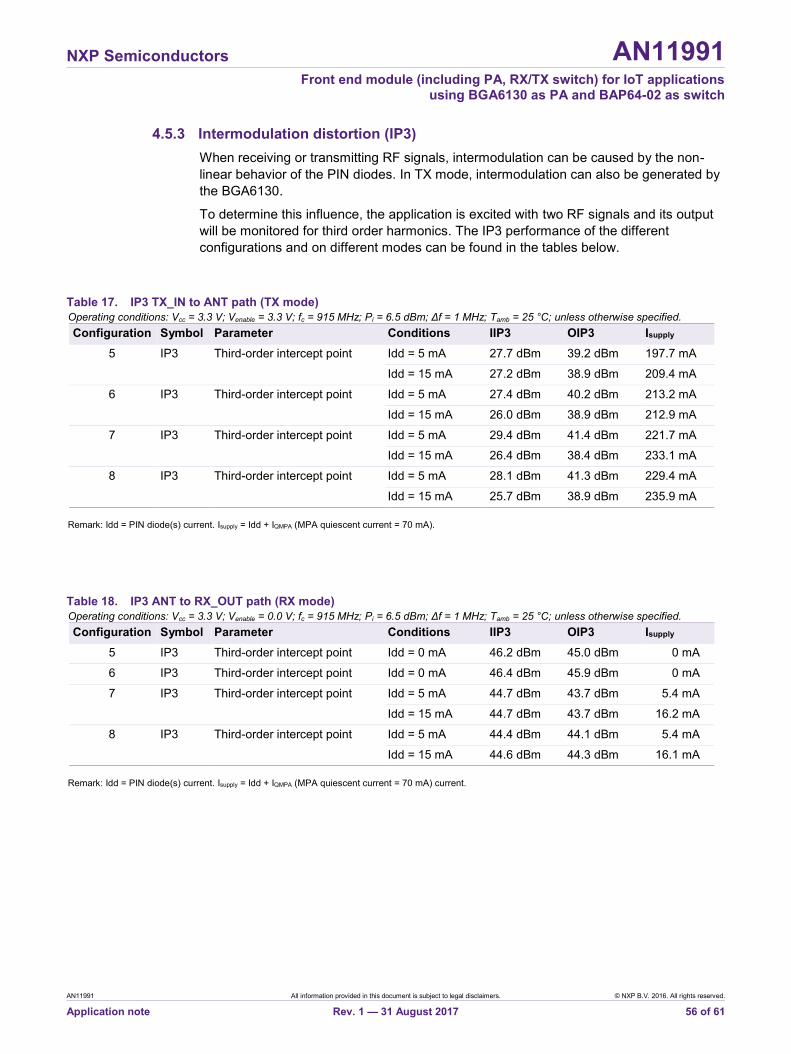
4.5.3 Intermodulation distortion (IP3) When receiving or transmitting RF signals, intermodulation can be caused by the non- linear behavior of the PIN diodes. In TX mode, intermodulation can also be generated by the BGA6130.
To determine this influence, the application is excited with two RF signals and its output will be monitored for third order harmonics. The IP3 performance of the different configurations and on different modes can be found in the tables below.
Table 17. IP3 TX_IN to ANT path (TX mode) Operating conditions: Vcc = 3.3 V; Venable = 3.3 V; fc = 915 MHz; Pi = 6.5 dBm; Δf = 1 MHz; Tamb = 25 °C; unless otherwise specified. Configuration Symbol Parameter Conditions IIP3 OIP3 Isupply
5 IP3 Third-order intercept point Idd = 5 mA 27.7 dBm 39.2 dBm 197.7 mA
Idd = 15 mA 27.2 dBm 38.9 dBm 209.4 mA
6 IP3 Third-order intercept point Idd = 5 mA 27.4 dBm 40.2 dBm 213.2 mA
Idd = 15 mA 26.0 dBm 38.9 dBm 212.9 mA
7 IP3 Third-order intercept point Idd = 5 mA 29.4 dBm 41.4 dBm 221.7 mA
Idd = 15 mA 26.4 dBm 38.4 dBm 233.1 mA
8 IP3 Third-order intercept point Idd = 5 mA 28.1 dBm 41.3 dBm 229.4 mA
Idd = 15 mA 25.7 dBm 38.9 dBm 235.9 mA
Remark: Idd = PIN diode(s) current. Isupply = Idd + IQMPA (MPA quiescent current = 70 mA).
Table 18. IP3 ANT to RX_OUT path (RX mode) Operating conditions: Vcc = 3.3 V; Venable = 0.0 V; fc = 915 MHz; Pi = 6.5 dBm; Δf = 1 MHz; Tamb = 25 °C; unless otherwise specified. Configuration Symbol Parameter Conditions IIP3 OIP3 Isupply
5 IP3 Third-order intercept point Idd = 0 mA 46.2 dBm 45.0 dBm 0 mA
6 IP3 Third-order intercept point Idd = 0 mA 46.4 dBm 45.9 dBm 0 mA
7 IP3 Third-order intercept point Idd = 5 mA 44.7 dBm 43.7 dBm 5.4 mA
Idd = 15 mA 44.7 dBm 43.7 dBm 16.2 mA
8 IP3 Third-order intercept point Idd = 5 mA 44.4 dBm 44.1 dBm 5.4 mA
Idd = 15 mA 44.6 dBm 44.3 dBm 16.1 mA
Remark: Idd = PIN diode(s) current. Isupply = Idd + IQMPA (MPA quiescent current = 70 mA) current.
NXP Semiconductors AN11991
Front end module (including PA, RX/TX switch) for IoT applications using BGA6130 as PA and BAP64-02 as switch
AN11991 All information provided in this document is subject to legal disclaimers. © NXP B.V. 2016. All rights reserved.
Application note Rev. 1 — 31 August 2017 57 of 61
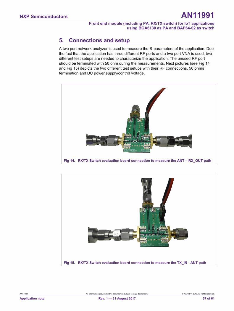
5. Connections and setup A two port network analyzer is used to measure the S-parameters of the application. Due the fact that the application has three different RF ports and a two port VNA is used, two different test setups are needed to characterize the application. The unused RF port should be terminated with 50 ohm during the measurements. Next pictures (see Fig 14 and Fig 15) depicts the two different test setups with their RF connections, 50 ohms termination and DC power supply/control voltage.
Fig 14. RX/TX Switch evaluation board connection to measure the ANT – RX_OUT path
Fig 15. RX/TX Switch evaluation board connection to measure the TX_IN - ANT path
Error!
Unknow
n docume
nt property nam
e.
Error! Unknow
n document property nam
e. E
rror! Unknow
n document property
name.
NXP Semiconductors AN11991 Front end module (including PA, RX/TX switch) for IoT applications
using BGA6130 as PA and BAP64-02 as switch
AN11991 All information provided in this document is subject to legal disclaimers. © NXP B.V. 2016. All rights reserved.
Application note Rev. 1 — 31 August 2017 58 of 61
6. Legal information
6.1 Definitions Draft — The document is a draft version only. The content is still under internal review and subject to formal approval, which may result in modifications or additions. NXP Semiconductors does not give any representations or warranties as to the accuracy or completeness of information included herein and shall have no liability for the consequences of use of such information.
6.2 Disclaimers Limited warranty and liability — Information in this document is believed to be accurate and reliable. However, NXP Semiconductors does not give any representations or warranties, expressed or implied, as to the accuracy or completeness of such information and shall have no liability for the consequences of use of such information. NXP Semiconductors takes no responsibility for the content in this document if provided by an information source outside of NXP Semiconductors.
In no event shall NXP Semiconductors be liable for any indirect, incidental, punitive, special or consequential damages (including - without limitation - lost profits, lost savings, business interruption, costs related to the removal or replacement of any products or rework charges) whether or not such damages are based on tort (including negligence), warranty, breach of contract or any other legal theory.
Notwithstanding any damages that customer might incur for any reason whatsoever, NXP Semiconductors’ aggregate and cumulative liability towards customer for the products described herein shall be limited in accordance with the Terms and conditions of commercial sale of NXP Semiconductors.
Right to make changes — NXP Semiconductors reserves the right to make changes to information published in this document, including without limitation specifications and product descriptions, at any time and without notice. This document supersedes and replaces all information supplied prior to the publication hereof.
Suitability for use — NXP Semiconductors products are not designed, authorized or warranted to be suitable for use in life support, life-critical or
safety-critical systems or equipment, nor in applications where failure or malfunction of an NXP Semiconductors product can reasonably be expected to result in personal injury, death or severe property or environmental damage. NXP Semiconductors and its suppliers accept no liability for inclusion and/or use of NXP Semiconductors products in such equipment or applications and therefore such inclusion and/or use is at the customer’s own risk.
Applications — Applications that are described herein for any of these products are for illustrative purposes only. NXP Semiconductors makes no representation or warranty that such applications will be suitable for the specified use without further testing or modification.
Customers are responsible for the design and operation of their applications and products using NXP Semiconductors products, and NXP Semiconductors accepts no liability for any assistance with applications or customer product design. It is customer’s sole responsibility to determine whether the NXP Semiconductors product is suitable and fit for the customer’s applications and products planned, as well as for the planned application and use of customer’s third party customer(s). Customers should provide appropriate design and operating safeguards to minimize the risks associated with their applications and products.
NXP Semiconductors does not accept any liability related to any default, damage, costs or problem which is based on any weakness or default in the customer’s applications or products, or the application or use by customer’s third party customer(s). Customer is responsible for doing all necessary testing for the customer’s applications and products using NXP Semiconductors products in order to avoid a default of the applications and the products or of the application or use by customer’s third party customer(s). NXP does not accept any liability in this respect.
Export control — This document as well as the item(s) described herein may be subject to export control regulations. Export might require a prior authorization from national authorities.
6.3 Trademarks Notice: All referenced brands, product names, service names and trademarks are property of their respective owners.
NXP Semiconductors AN11991
Front end module (including PA, RX/TX switch) for IoT applications using BGA6130 as PA and BAP64-02 as switch
AN11991 All information provided in this document is subject to legal disclaimers. © NXP B.V. 2016. All rights reserved.
Application note Rev. 1 — 31 August 2017 59 of 61
7. List of figures
Fig 1. RX/TX Switch evaluation board ........................ 3 Fig 2. RX/TX Switch evaluation board with BGA6130 . 3 Fig 3. Circuit diagram of the RX/TX Switch evaluation
board narrow band configuration ...................... 8 Fig 4. Circuit diagram of the RX/TX Switch evaluation
board broadband configuration ......................... 9 Fig 5. EVB layout broadband configuration ................. 9 Fig 6. Printed-Circuit Board layout of the RX/TX Switch
evaluation board without BGA6130. ................ 10 Fig 7. Stack of the PCB material ............................... 11 Fig 8. Circuit diagram of the RX/TX Switch with
BGA6130 evaluation board narrow band configuration ................................................... 33
Fig 9. Circuit diagram of the RX/TX Switch with BGA6130 evaluation board broadband configuration ................................................... 34
Fig 10. EVB layout broadband configuration ............... 34 Fig 11. Printed-Circuit Board layout of the RX/TX Switch
evaluation board with BGA6130. ..................... 35 Fig 12. Recommended BGA6130 thermal via placement
........................................................................ 36 Fig 13. Stack of the PCB material ............................... 36 Fig 14. RX/TX Switch evaluation board connection to
measure the ANT – RX_OUT path ................. 57 Fig 15. RX/TX Switch evaluation board connection to
measure the TX_IN - ANT path ....................... 57
NXP Semiconductors AN11991
Front end module (including PA, RX/TX switch) for IoT applications using BGA6130 as PA and BAP64-02 as switch
AN11991 All information provided in this document is subject to legal disclaimers. © NXP B.V. 2016. All rights reserved.
Application note Rev. 1 — 31 August 2017 60 of 61
8. List of tables
Table 1. Configuration overview ..................................... 4 Table 2. Summary measurement results ........................ 6 Table 3. BOM of the RX/TX switch evaluation board
configuration 1 (narrow band + low pass filter) 12 Table 4. BOM of the RX/TX switch evaluation board
configuration 2 (narrow band) ......................... 12 Table 5. BOM of the RX/TX switch evaluation board
configuration 3 (broadband + low pass filter) .. 13 Table 6. BOM of the RX/TX switch evaluation board
configuration 4 (broadband) ............................ 13 Table 7. S-parameter summary .................................... 27 Table 8. IP3 TX_IN to ANT path (TX mode) ................. 29 Table 9. IP3 ANT to RX_OUT path (RX mode) ............. 29 Table 10. Summary measurement results ...................... 31 Table 11. BOM of the RX/TX switch evaluation board
configuration 5 (narrow band + MPA + low pass filter) ................................................................ 37
Table 12. BOM of the RX/TX switch evaluation board configuration 6 (narrow band + MPA) ............. 38
Table 13. BOM of the RX/TX switch evaluation board configuration 7 (broad band + MPA + low pass filter) ................................................................ 39
Table 14. BOM of the RX/TX switch evaluation board configuration 8 (broad band + MPA) ............... 40
Table 15. S-parameter summary .................................... 54 Table 16. TX_INT to ANT path with BGA6130 (TX mode)
........................................................................ 55 Table 17. IP3 TX_IN to ANT path (TX mode) ................. 56 Table 18. IP3 ANT to RX_OUT path (RX mode) ............. 56
NXP Semiconductors AN11991
Front end module (including PA, RX/TX switch) for IoT applications using BGA6130 as PA and BAP64-02 as switch
Please be aware that important notices concerning this document and the product(s) described herein, have been included in the section 'Legal information'.
© NXP B.V. 2016. All rights reserved.
For more information, visit: http://www.nxp.com For sales office addresses, please send an email to: [email protected]
Date of release: 31 August 2017 Document identifier: AN11991
9. Contents
1. Introduction ......................................................... 3 2. General description ............................................. 4 3. RX/TX switch evaluation board .......................... 5 3.1 Summary measurement results ......................... 6 3.2 Application Circuit .............................................. 8 3.3 PCB Layout ...................................................... 10 3.4 Bill of materials ................................................. 12 3.5 Measurement results ........................................ 14 3.5.1 S-parameters (3-port) ....................................... 14 3.5.1.1 Narrow band with low-pass filter (configuration 1)
......................................................................... 15 3.5.1.2 Narrow band without filter (configuration 2) ...... 18 3.5.1.3 Broad band with filter (configuration 3) ............. 21 3.5.1.4 Broad band without filter (configuration 4) ........ 24 3.5.2 In-band 1dB gain compression ......................... 28 3.5.3 Intermodulation distortion (IP3) ........................ 29 4. RX/TX switch with MPA evaluation board ....... 30 4.1 Summary measurement results ....................... 31 4.2 Application Circuit ............................................ 33 4.3 PCB Layout ...................................................... 35 4.4 Bill of materials ................................................. 37 4.5 Measurement results ........................................ 41 4.5.1 S-parameters (3-port) ....................................... 41 4.5.1.1 Narrow band with BGA6130 and filter
(configuration 5) ............................................... 42 4.5.1.2 Narrow band with BGA6130 without filter
(configuration 6) ............................................... 45 4.5.1.3 Board band with BGA6130 with filter
(configuration 7) ............................................... 48 4.5.1.4 Broad band with BGA6130 without filter
(configuration 8) ............................................... 51 4.5.2 In-band 1dB gain compression ......................... 55 4.5.3 Intermodulation distortion (IP3) ........................ 56 5. Connections and setup ..................................... 57 6. Legal information .............................................. 58 6.1 Definitions ........................................................ 58
6.2 Disclaimers ....................................................... 58 6.3 Trademarks ...................................................... 58 7. List of figures ..................................................... 59 8. List of tables ...................................................... 60 9. Contents ............................................................. 61