an optical metrology tool with si wafer form factor
TRANSCRIPT

1
FLCC Seminar 10/8/2007FLCC Seminar 10/8/2007
An Optical Metrology ToolAn Optical Metrology ToolWith With Si Si Wafer Form FactorWafer Form Factor
Nathan W. CheungDept of EECS UC-Berkeley

2
OUTLINEOUTLINE
• Unique features of optical metrology wafer• Wafer Fabrication• Reflectance Simulations• Applications: RIE, CMP, Wet Etch• Lateral Features Monitoring• Extension to Optical Spectroscopy

3
Unique FeaturesUnique FeaturesData Transmission
Photo/RF Transmitter
Dielectric Layer as Optical Window
Si
Battery Data Acquisition Unit
500µm
■ Durable in hostile processing environments such as in plasma, wet etching, and CMP■Self-contained metrology unit with power and data acquisition■Real Time Process ControlLocation specific, real time measurements. Pinpoint failure
and cause.

4
Thin LED by Laser LiftoffThin LED by Laser Liftoff1.1. Bond receptor Bond receptor
onto GaN2. Laser Liftoff (LLO)2. Laser Liftoff (LLO)
onto GaNb) thermal
detachment (40°C)
a) interfacial decomposition
receptor wafer
Al2O3
epoxyGaN
KrF pulsedexcimer laser
5
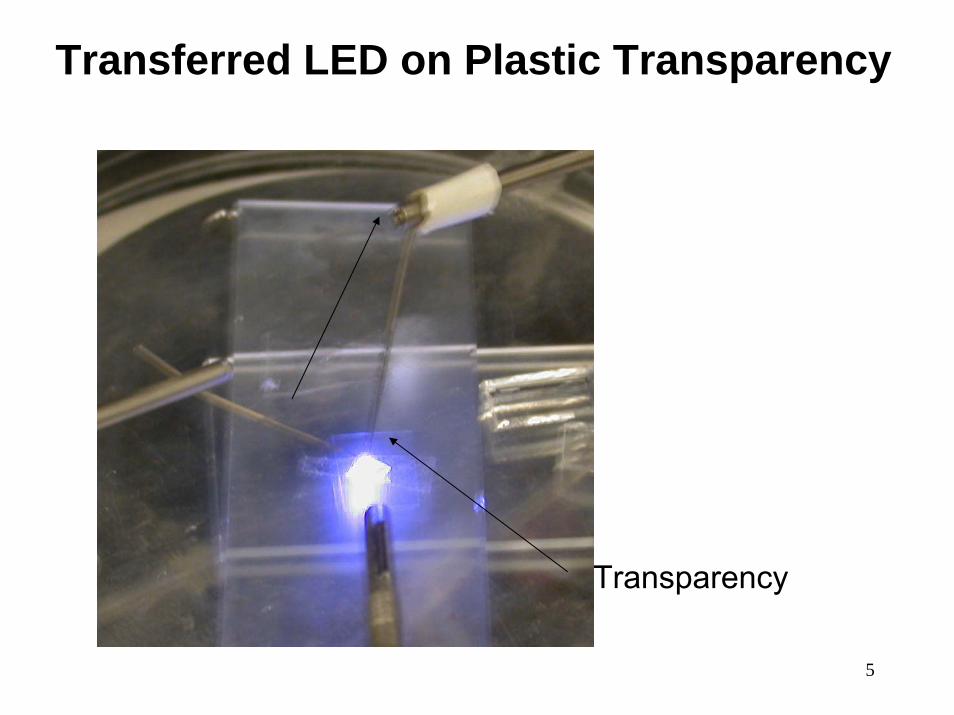
Transferred LED on Plastic Transparency
Transparency

6
Paper-Thin Photon Engine by Laser Liftoff(> 100 Lumens/Watt)

7
High Brightness LED as Photon Source
Specular Reflection
0.0E+00
2.0E-05
4.0E-05
6.0E-05
8.0E-05
1.0E-04
1.2E-04
0 5 10 15 20 25 30
Time [s]
Cur
rent
[A] Room Light
room Light + LED
Room Light + LED +Flashlight
•Specular reflection from room lights is almost negligible
•Specular reflection from strong point sources can add significant noise to system
8
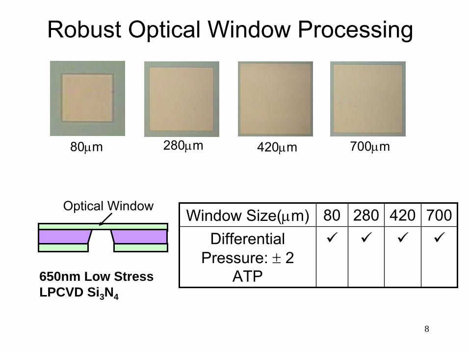
Robust Optical Window Processing
80µm 700µm280µm 420µm
Optical WindowWindow Size(µm) 80 280 420 700
Differential Pressure: ± 2
ATP650nm Low Stress LPCVD Si3N4

9
3X3 multi-pixel metrology wafer platform
LED
Photo Switch
Battery

Optical Metrology by ReflectanceExample: Thickness Monitoring of SiO2 Film
Calculated Reflectance
Ref
lect
ance
(R)
Thickness of Deposited SiO2 film (µm)
Dp=137.5 nm
θ=0°, λ = 525 nm
hνo
R
T
Window Si: 20 nmWindow SiO2:
2.4 µm
Deposited SiO2
10
Determination of thickness change:1.Calibrate periodicity in time domain (tp) with that in spacial domain (Dp).2. Thickness change:= Dp(process time span/tp).
R
Process time
Expected Experimental data

LED Spectral Distribution EffectLED Spectral Distribution Effect
400 420 440 460 480 500 520 5400
500
1000
1500
2000
2500
3000
Ele
ctro
lum
ines
cenc
e
Wavelength (nm)
I0
I-1 I+1
Electroluminescence spectra of GaN-based LEDs
Simulation Condition:Vacuum ambient, Cu thin film, Incident angle, θ, = 40°, Si3N4 window thickness 649nm, the refractive index of Cu: n=1.16,k=2.43*.
Optical response is very sensitive to the wavelength.
LED spectral distribution will limit Cu thickness resolution to <2 nm at end-point(depending on the incident angle), assuming a signal resolution of 5% of actual signal.
0 20 40 60 80 1000.0
0.1
0.2
0.3
0.4
Effe
ctiv
e re
flect
ance
Cu thickness (nm)
I0
I-1
I+1
Itotal = I0 + I-1 + I+1
θ = 40°
I
RT
Si3N4
Cu
11

12
Choice of Optical Window MaterialsChoice of Optical Window Materials
0 20 40 60 80 1000.0
0.1
0.2
0.3
0.4
0.5
0.6
0.7
0.8
θi = 20o
θi = 40o
θi = 60o
θi = 80o
Ref
lect
ance
Cu Thickness (nm)
Simulation Condition:Vacuum ambient, Cu thin film, window thickness 649nm, LED peak wavelength 463nm, the refractive index of Cu: n=1.16, k=2.43.
*D.L. Windt, IMD Software.
0 20 40 60 80 100
0.0
0.1
0.2
0.3
0.4
0.5
0.6
0.7
0.8
θi = 20o
θi = 40o
θi = 60o
θi = 80o
Ref
lect
ance
Cu Thickness (nm)
Si3N4 Optical window SiO2 Optical window
Signal sensing depends greatly on incident angle.Si3N4 optical window shows more signal variation before end-point.

13
Calibration MethodologyCalibration Methodology
0 20 40 60 80 100 1200
50
100
150
200
250
PP
D re
adin
g (a
.u.)
RPD reading (a.u.)
Air (Slope=1.901+0.002) Water (Slope=1.552+0.001) P.R. (Slope=1.417+0.001)The current metrology is relied on the changes
in a reflected optical signal through an optical window
Good linearity was confirmed between PPD and RPD reading, suggesting the valid assumptions made in the current methodology.
A new function F may be used to eliminate non-measurable constants such optical component misalignment
0
0
0
0
)/()/()/(
RP
RPRP
P
PP
VVVVVV
F
RRRF
δδδδδδ −
=
−≡
Primary Photo-Detector (PPD)
LEDθi
Reference Photo-Detector (RPD)
Dielectric Window
RRRP
Film to be grown/etched
Primary Photo-Detector (PPD)
LEDθi
Reference Photo-Detector (RPD)
Dielectric Window
RRRP
Film to be grown/etched
Steve Luo, PhD Thesis, UCB

14
Verification of methodology
100 150 200 250 300 350 400390
400
410
420
430
440
V r(a.u
.)
Vc (a.u.)
Air (slope=0.132+0.002) Water (slope=0.118+0.005)
Results Summary:Good linearity was confirmed between PPD reading and RPD reading. Using data fitting, incident angle was determined to be about 70 degree, which agrees well with the geometric configuration used.
Optical Window: 650nm Si3N4;Window Size: 4mm;Photodetector Active Area: 10mm2;LED peak wavelength: 463nm.
Dielectric Layer
RPD PPD LED

15
Refractive Index Measurments
0 20 40 60 80 100 1200
20
40
60
80
100
120
140PP
D re
adin
g (a
.u.)
RPD reading (a.u.)
Air (slope=1.1677+0.0006) Water (slope=1.0988+0.0005) PR (slope=1.0745+0.0005)
Refractive index sensitivity better than 0.001

16
Plasma Etching of Si Oxide
Plasma Etch Measurements
Metrology Wafer
HP 4145B
Wire Connection Interface
Detection Window
Measuring oxide thickness using Dektak3030 Profilometer
Plasma
PQECR, Plasma Quest

17
Calibration with a Plasma Etch Process of Silicon Oxide
0 20 40 60 80 100 120 140 160 180 200
-0.8
-0.6
-0.4
-0.2
0.0
0.2
F(θ)
Oxide Thickness (nm)
Experimental Fitted
The good fit between experimental data and calculation demonstrated that the methodology worked as expected.
As expected, effective incident angle, detection window thickness and even effective incident wavelength can be determined by a calibration process.
•n.a.•(1.464,0)*•(nf, kf)•n.a.•(2.054,0)*•(nw, kw)•649•650 ±7•dw (nm)•56•n.a.•θi (°)•n.a.•463 (peak)•λ (nm)
•Extracted•Measured
*D.L. Windt, IMD Software.

18
Simulation: Response Space for Copper End-Point Etch Detection
Simulation Conditions: Vacuum ambient inside the metrology wafer and water ambient outside the metrology wafer. SiO2 thickness: 500 um
I
R
T
SiO2
Cu
nm463=λ
0
0.1
0.2
0.3
0.4
0.5
0.6
0.7
0.8
0.9
1
-20020406080
Copper Thickness [nm]
Ref
lect
ance
[R]
15 deg30 deg45 deg60 deg75 deg

19
Demo: Copper Wet Etch End-Point Detection
0
0.00005
0.0001
0.00015
0.0002
0.00025
0 5 10 15 20
Time [s]
Cur
rent
[A]
200 nm150 nm100 nm
Data sample rate: 10 Hz
Stage I Stage II
Multi-stage mechanism of Cu etching.
50 nm Cu
0 nm Cu
20
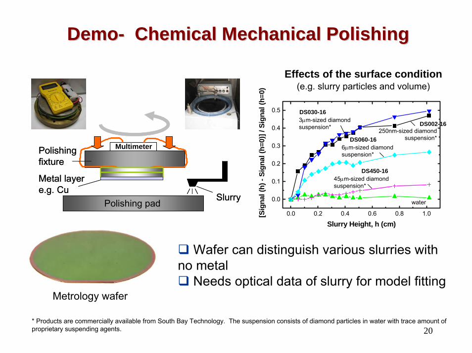
DemoDemo-- Chemical Mechanical Polishing Chemical Mechanical Polishing
Wafer can distinguish various slurries with no metal
Needs optical data of slurry for model fitting
Metal layer e.g. Cu
Polishing fixture
SlurryPolishing pad
Multimeter
Metal layer e.g. Cu
Polishing fixture
SlurryPolishing pad
Multimeter
Metrology wafer
Effects of the surface condition(e.g. slurry particles and volume)
0.0 0.2 0.4 0.6 0.8 1.0
0.0
0.1
0.2
0.3
0.4
0.5
[Sig
nal (
h) -
Sign
al (h
=0)]
/ Sig
nal (
h=0)
Slurry Height, h (cm)
water
45µm-sized diamond suspension*
250nm-sized diamond suspension*
3µm-sized diamond suspension*
6µm-sized diamond suspension*
DS002-16
DS030-16
DS060-16
DS450-16
* Products are commercially available from South Bay Technology. The suspension consists of diamond particles in water with trace amount of proprietary suspending agents.

21
Simulation*: Lateral Feature WettingGoal: Simulate monitoring of wetting in high aspect ratio contact
holes in dielectrics.
Effective Medium Approximation:
Effective refractive index of each layer = Volume fraction of A*(na+ika) + Volume fraction of B*(nb+ikb)
Valid as long as layer thickness and lateral dimensions of features are less than wavelength of photon.
*D. L. Windt - IMD Software
0% 25% 50% 75% 100%
Al2O3
Water
SiO2

22
0.00011
0.00012
0.00013
0.00014
0.00015
0 20 40 60 80 100 120 140 160 180 200
Time [s]
Cur
rent
[A]
M1M2M3
Demo: Wetting of 200nm contact holes
Methanol observed to wet the sample.
• Reflectivity can monitor liquid wetting of 200 nm contact holes.
• Promising to monitor liner deposition in high-aspect ratio contact holes
Top SEM Side SEMTop SEM Side SEM

23
IMPACT: Metrology Wafer With Spectroscopy Capability
Si3N4, SiO2 Stack
Cavity
Optical Window
Bulk Silicon WaferWhite PhosphorLED* PD Array*
Photo/RF Transmitter*
Data TransmissionMolecules
Multilayer Diffraction Stack
several mm*Internal Power Source Not Shown
500 um
• Durable in hostile processing environments such as in plasma, wet etching, and CMP*;
• Identification of chemical precursors• Temporal information for chemical kinetics
*Please see previous FLCC reports on metrology wafer construction, plasma etching results, copper end-point detection, and CMP results.

24
Technical Approach: Multilayer Diffraction Stack
Light in
Mirror (Metal)Mirror (Metal)
Multilayer thin-film stack
~few um thick
1x 2x 3xPhotodiode array
Slit
Lateral length can be on the mm scale
Light out
• 10 um detector pixel gives 50 nm wavelength resolution.

25
Technical Approach: Blue LED Phosphors for Broadband Spectroscopy
Excitation Emission
0102030405060708090
100
380 430 480 530 580 630 680 730 780
Wavelength (nm)
Inte
nsity
(a.u
.)
TYPE QUMK58/F-D1YTTRIUM GADOLINIUM ALUMINIUM OXIDE : CERIUM
(Y,Gd)3Al5O12 : Ce
Yellow
Excitation Emission
0
10
20
30
40
50
60
70
80
90
100
250 300 350 400 450 500 550 600 650 700 750 800
Wavelength (nm)
Inte
nsity
(a.u
.)
TYPE FL63/S-D1CALCIUM SULPHIDE : EUROPIUM CaS : Eu
Excitation Emission
0
10
20
30
40
50
60
70
80
90
100
250 300 350 400 450 500 550 600 650 700 750 800
Wavelength (nm)
Inte
nsity
(a.u
.)
TYPE HPL63/F-F1STRONTIUM THIOGALLATE : EUROPIUM SrGa2S4 : Eu
GreenRed

26
Bio-Analytical Microsystem
CdS Filter
Microfluidic channel
PIN Diode
LED PixelLED exciting Fluidic Channel
0 1x10⁻⁶ 2x10⁻⁶ 3x10⁻⁶ 4x10⁻⁶ 5x10⁻⁶ 6x10⁻⁶ 7x10-60.0
0.2
0.4
0.6
0.8
1.0
1.2
1.4
1.6
1.8
2.0
2.2
2.4
0.35 V 0.30 V 0.25 V 0.20 V 0.15 V
Det
ecto
r Sig
nal (
mV)
Concentration (M)
Sensitivity ≤ 1×10⁻⁷ M
•Fluorescence detection limit better than 1×10⁻⁷ M.
5mm
CdS filter
CdS0.9Se0.1 filterLED
5mm
Green LED
Blue LED
5mm
CdS filter
CdS0.9Se0.1 filterLED
5mm5mm5mm
CdS filter
CdS0.9Se0.1 filterLED
5mm
Green LED
Blue LED5mm5mm5mm
Green LED
Blue LED
Cheung (EECS) Lee (BioEng)Sands (Purdue)

27
Ubiquitous Blue LaserUbiquitous Blue Laser
0 50 100 150 200 250 3000
20
40
60
80
100
CW 20oC
Ligh
t Out
put
(mW
)
Current (mA)
Blue Laser Diode onCu Substrate
Laser diode on Cu ηD = 0.5 W/A
Laser Diode Array Transfer
W.S. Wong et al., Compound Semiconductor 7, 47 (2001)
Laser diode on sapphire
Improved light output due to better thermal management

28
New Application AreasOptical Interference
Function (FLCC)Spectroscopy Capability
(IMPACT) Future Areas of Interest
Refractive Index Monitoring Molecular Fluorescence Spectroscopy (MFS)
Thermal/Chemical/Mechanical Induced Optical
ChangesResist Development/Stripping* Precursor Identification
ScatteringCopper End-point Etch Detection* Interface Chemical Kinetics
Phase ShiftPlasma Etch* Reaction Rate Modeling
Non-Linear Optics
CMP* Deposition Key Expected Results:• Time domain optical data• Kinetics of chemical reactions and fabprocesses.
Lateral Feature Monitoring Wet and Dry Etching
Thin Film Thickness Resist Development
*Please see previous FLCC reports on metrology wafer construction, plasma etching results, copper end-point detection, and CMP results.