an investigation into the fabrication of nanomechanical switches
TRANSCRIPT

An Investigation into the Fabrication ofNanomechanical Switches
by
Carlo Schenke
Thesis presented in partial fulfilment of the requirements forthe degree of Master of Science in Engineering at
Stellenbosch University
Supervisor: Prof. W.J. PeroldDepartment of Electrical and Electronic Engineering
March 2010

Declaration
By submitting this thesis electronically, I declare that the entirety of the workcontained therein is my own, original work, that I am the owner of the copy-right thereof (unless to the extent explicitly otherwise stated) and that I havenot previously in its entirety or in part submitted it for obtaining any qualifi-cation.
March 2010
Copyright © 2010 Stellenbosch UniversityAll rights reserved.

Abstract
This report intends to show how able the Stellenbosch Electrical and Elec-tronic Engineering Department’s micro fabrication laboratory is to manu-facture nanomechanical switches and similar structures. Following the inves-tigation, an attempt will be made to produce these devices.
In attaining this goal, a literature study was performed focusing on mech-anical switching and nanotechnology. Their origins, development and currentapplication are investigated, as well as the requirements for developing thesedevices.
Having completed the literature study, a series of current nanomechanicalswitches where investigated, selecting those most likely to be manufactured atthe available facilities and having the required attributes for taking the placeof silicon transistors in low speed, hostile environments.
The most common method of manufacturing nanoswitches is simulated us-ing several methods of predicting device failure. This will aid in the selection ofmanufacturing process guidelines, such as dimensions in the photoresist tem-plates and layer thickness before etching, allowing for the repeated productionof functional switches.
The two manufacturable nanomechanical switches are investigated, usingtechniques and materials available at the micro fabrication laboratory to manu-facture them. Subsequently, their electrical properties will be determined andused in simulating their failure characteristics.
In conclusion, the result are discussed along with advice and improvementsfor the continued investigation and production of nanodevices at StellenboschUniversity.
ii

Opsomming
Die doel met hierdie tesis is om die vermoë van die Departement Elektriese enElektroniese Ingenieurswese se mikro-elektronika laboratorium te ondersoekten opsigte van die vervaardiging van nanomeganiese skakelaars en aanver-wante komponente. Na afloop van die ondersoek sal ’n poging aangewendword om hierdie toestelle te vervaardig.
In nastrewing van hierdie doel is ’n literatuurstudie uitgevoer wat fokus opmeganiese skakeling en nanotegnologie. Die oorsprong, ontwikkeling en huidigeaanwending van hierdie skakelaars word ondersoek, sowel as die vereistes virdie ontwikkeling daarvan.
Na voltooiing van die literatuurstudie word ’n reeks van bestaande nano-meganiese skakelaars ondersoek. Skakelaars word dan geïdentifiseer op grondvan hul waarskynlike vervaardigbaarheid met die beskikbare fasiliteite. Dievereiste eienskappe vir lae spoed toepassings in omgewings waar silikon-skakelaarsnie kan werk nie, word ook in ag geneem.
Die mees algemene metode vir die vervaardiging van nanoskakelaars wordgesimuleer met behulp van verskeie tegnieke wat toestelfaling voorspel. Diesimulasies sal help in die keuse van vervaardigingsriglyne van die proses, soosdie dimensies van die fotolak template en die laagdiktes voor etsing, sodatgoeie resultate verkry kan word wanneer die skakelaars vervaardig word, metgoeie herhaalbaarheid.
Die twee gekose vervaardigbare nanomeganiese skakelaars word dan on-dersoek ten opsigte van die tegnieke en materiale wat in die mikro-elektronikalaboratorium beskikbaar is. Daarna sal die elektriese eienskappe van die skake-laars bepaal word.
Ter afsluiting word die resultate bespreek, saam met aanbevelings vir dievoortsetting van die navorsing om nanomeganiese skakelaars by die Universiteitvan Stellenbosch te vervaardig.
iii

Acknowledgements
I would like to thank my parents, Richard and Tertia Sandra Schenke, for theirlove and unwavering support.
A word of thanks to my supervisor, Prof W.J. Perold, for all the aid and guid-ance.
My appreciation to Gareth van der Westhuizen for all the evenings stuck inthe laboratory.Much of what was done in this report would not have been viable withoutthe help of Ulrich Büttner and the people at SED. Thanks to Ulrich Büttner,Wessel Croukamp, Lincon Saunders en Nicklaas van Graan.
Also to iThemba Labs I would like to express my appreciation for providingmaterials for the construction process.Lastly a thank you to all the family and friends that kept me going in the hardtimes.
iv

Contents
Declaration i
Abstract ii
Opsomming iii
Acknowledgements iv
Contents v
List of Figures viii
List of Tables xi
Nomenclature xii
1 Introduction 11.1 Research Objectives and Motivation . . . . . . . . . . . . . . . . 21.2 Report Overview . . . . . . . . . . . . . . . . . . . . . . . . . . 2
2 Literature Study 32.1 Steam powered thinking . . . . . . . . . . . . . . . . . . . . . . 32.2 Nanotechnology and NEMS . . . . . . . . . . . . . . . . . . . . 142.3 To summarise . . . . . . . . . . . . . . . . . . . . . . . . . . . . 35
3 Mechanical Nanoswitches 363.1 Device overview . . . . . . . . . . . . . . . . . . . . . . . . . . . 363.2 Silver Sulfide Switches . . . . . . . . . . . . . . . . . . . . . . . 373.3 Photoswitches . . . . . . . . . . . . . . . . . . . . . . . . . . . . 403.4 Carbon Nanotube Switches . . . . . . . . . . . . . . . . . . . . . 43
v

CONTENTS vi
3.5 Organically Actuated Switches . . . . . . . . . . . . . . . . . . . 463.6 To Summarise . . . . . . . . . . . . . . . . . . . . . . . . . . . . 48
4 Procedure and Methodology 494.1 Procedure . . . . . . . . . . . . . . . . . . . . . . . . . . . . . . 494.2 Methodology . . . . . . . . . . . . . . . . . . . . . . . . . . . . 514.3 To Summarise . . . . . . . . . . . . . . . . . . . . . . . . . . . . 51
5 Design and Manufacture 525.1 About the Microelectronics Laboratory . . . . . . . . . . . . . . 525.2 Basic Procedures in the Microelectronics Laboratory . . . . . . 565.3 Choosing a Device . . . . . . . . . . . . . . . . . . . . . . . . . 665.4 Manufacture . . . . . . . . . . . . . . . . . . . . . . . . . . . . . 685.5 Results . . . . . . . . . . . . . . . . . . . . . . . . . . . . . . . . 865.6 To Summarise . . . . . . . . . . . . . . . . . . . . . . . . . . . . 91
6 Simulation 926.1 CNT Simulation Theory . . . . . . . . . . . . . . . . . . . . . . 936.2 Implementation of Simulation Theory . . . . . . . . . . . . . . . 966.3 To Summarise . . . . . . . . . . . . . . . . . . . . . . . . . . . . 103
7 Conclusion 104
Appendices 107
A Clean Room 108A.1 Servicing Procedure . . . . . . . . . . . . . . . . . . . . . . . . . 108A.2 Clean room Rules and Regulations . . . . . . . . . . . . . . . . 110A.3 Personnel Entrance Procedure . . . . . . . . . . . . . . . . . . . 112A.4 Emergencies . . . . . . . . . . . . . . . . . . . . . . . . . . . . . 113
B Deposition Materials 114
C XRD Results 118C.1 Calibration Sample . . . . . . . . . . . . . . . . . . . . . . . . . 118C.2 Silver . . . . . . . . . . . . . . . . . . . . . . . . . . . . . . . . . 120C.3 Silver Sulfide . . . . . . . . . . . . . . . . . . . . . . . . . . . . 121C.4 Palladium . . . . . . . . . . . . . . . . . . . . . . . . . . . . . . 122

CONTENTS vii
C.5 Aluminium . . . . . . . . . . . . . . . . . . . . . . . . . . . . . 123
List of References 124
List of Figures
2.1 A box of Napier’s bones . . . . . . . . . . . . . . . . . . . . . . . . 32.2 Schickardt’s mechanical calculator . . . . . . . . . . . . . . . . . . . 42.3 Pascal’s computer . . . . . . . . . . . . . . . . . . . . . . . . . . . . 52.4 Leibnitz’s geared calculating machine . . . . . . . . . . . . . . . . . 52.5 Charles Babbage . . . . . . . . . . . . . . . . . . . . . . . . . . . . 62.6 Difference Engine Nr 2 replica . . . . . . . . . . . . . . . . . . . . . 112.7 Lego Difference Engine . . . . . . . . . . . . . . . . . . . . . . . . . 122.8 A visual relation of scales . . . . . . . . . . . . . . . . . . . . . . . 152.9 AFM theory . . . . . . . . . . . . . . . . . . . . . . . . . . . . . . . 182.10 STM theory . . . . . . . . . . . . . . . . . . . . . . . . . . . . . . . 182.11 Representation of TEM and SEM microscopy . . . . . . . . . . . . 202.12 The photolithography process . . . . . . . . . . . . . . . . . . . . . 252.13 The effects of positive and negative photoresist . . . . . . . . . . . 262.14 Dip pen nanolithography setup . . . . . . . . . . . . . . . . . . . . 272.15 Self assembled polymer sheet . . . . . . . . . . . . . . . . . . . . . 292.16 Magnetically folded blank . . . . . . . . . . . . . . . . . . . . . . . 302.17 Drug capsule after completion . . . . . . . . . . . . . . . . . . . . . 302.18 Nano-origami procedure . . . . . . . . . . . . . . . . . . . . . . . . 30
3.1 Silver sulfide as an ionic conductor . . . . . . . . . . . . . . . . . . 373.2 Silver sulfide switch model . . . . . . . . . . . . . . . . . . . . . . . 383.3 Silver sulfide reversable particle model . . . . . . . . . . . . . . . . 393.4 Schematic and topographic views of a phototransistor . . . . . . . . 403.5 Model of a F16CuPc photoswitch . . . . . . . . . . . . . . . . . . . 413.6 Functional model of the organic insulator photoswitch . . . . . . . . 413.7 Representation and SEM image of a basic CNT switch . . . . . . . 433.8 Model of the CNT trench switch . . . . . . . . . . . . . . . . . . . 44
viii

LIST OF FIGURES ix
3.9 Model of the telescoping nanoswitch . . . . . . . . . . . . . . . . . 453.10 C70 Switch model . . . . . . . . . . . . . . . . . . . . . . . . . . . . 453.11 Nanomotor from liquid spheres . . . . . . . . . . . . . . . . . . . . 463.12 Organically actuated contact switch . . . . . . . . . . . . . . . . . . 47
5.1 Nick van Graan working in the cleanroom (1986) . . . . . . . . . . 525.2 Transistor manufactured in microelectronics laboratory . . . . . . . 535.3 Photoresist spinner and associated chemicals . . . . . . . . . . . . . 565.4 UV exposer . . . . . . . . . . . . . . . . . . . . . . . . . . . . . . . 575.5 Chrome Mask . . . . . . . . . . . . . . . . . . . . . . . . . . . . . . 585.6 PCB mask . . . . . . . . . . . . . . . . . . . . . . . . . . . . . . . . 585.7 Printed mask . . . . . . . . . . . . . . . . . . . . . . . . . . . . . . 585.8 Rubber mask . . . . . . . . . . . . . . . . . . . . . . . . . . . . . . 585.9 Photoresist profile of a chrome mask . . . . . . . . . . . . . . . . . 595.10 Photoresist profile of a PCB mask . . . . . . . . . . . . . . . . . . . 595.11 Photoresist profile of a printed mask . . . . . . . . . . . . . . . . . 595.12 Photoresist profile of a rubber mask . . . . . . . . . . . . . . . . . . 595.13 Thermal evaporation unit . . . . . . . . . . . . . . . . . . . . . . . 615.14 Thermal evaporation unit crucible . . . . . . . . . . . . . . . . . . . 625.15 Thermal evaporation unit during annealing process . . . . . . . . . 625.16 QCM sensor and housing . . . . . . . . . . . . . . . . . . . . . . . . 635.17 AFM station . . . . . . . . . . . . . . . . . . . . . . . . . . . . . . 645.18 The AFM and motorised sample base . . . . . . . . . . . . . . . . . 645.19 Test run photoswitches . . . . . . . . . . . . . . . . . . . . . . . . . 685.20 Diagram for thin film theory . . . . . . . . . . . . . . . . . . . . . . 705.21 Organic layer components and equipment . . . . . . . . . . . . . . . 725.22 Polystyrene spun on at 3000rpm . . . . . . . . . . . . . . . . . . . . 735.23 Polystyrene spun on at 4000rpm . . . . . . . . . . . . . . . . . . . . 735.24 Polystyrene spun on at 5000rpm . . . . . . . . . . . . . . . . . . . . 735.25 Graph for layer thicknesses . . . . . . . . . . . . . . . . . . . . . . . 745.26 Colour map AFM scan an organic layer . . . . . . . . . . . . . . . . 755.27 3D graph AFM scan of an organic layer . . . . . . . . . . . . . . . 755.28 3D graph AFM scan of a scratched organic layer . . . . . . . . . . . 755.29 Cross section of the AFM scratch . . . . . . . . . . . . . . . . . . . 765.30 Cross section along the AFM scratch . . . . . . . . . . . . . . . . . 775.31 First complete photoswitch . . . . . . . . . . . . . . . . . . . . . . 78

LIST OF FIGURES x
5.32 3D graph AFM scan of the ITO glass . . . . . . . . . . . . . . . . . 785.33 Cross section of the ITO glass surface . . . . . . . . . . . . . . . . . 785.34 SEM image of an actual Ag2S switch . . . . . . . . . . . . . . . . . 795.35 Niello Silverware . . . . . . . . . . . . . . . . . . . . . . . . . . . . 805.36 Liver of sulphur . . . . . . . . . . . . . . . . . . . . . . . . . . . . . 815.37 The impregnated silver tested in nitric acid . . . . . . . . . . . . . 815.38 The impregnation solution and heating base . . . . . . . . . . . . . 825.39 Impregnated silver samples . . . . . . . . . . . . . . . . . . . . . . . 825.40 XRD sample holder . . . . . . . . . . . . . . . . . . . . . . . . . . . 835.41 XRD results for silver sulfide development . . . . . . . . . . . . . . 835.42 Test run device for the silver sulfide switch . . . . . . . . . . . . . . 845.43 Photoswitch testing area . . . . . . . . . . . . . . . . . . . . . . . . 865.44 UV exposure zone . . . . . . . . . . . . . . . . . . . . . . . . . . . . 865.45 Photoswitch with water cavitation . . . . . . . . . . . . . . . . . . 875.46 Layer damage from water drops . . . . . . . . . . . . . . . . . . . . 875.47 Aluminium distortion transition . . . . . . . . . . . . . . . . . . . . 885.48 Magnified view of aluminium deformation . . . . . . . . . . . . . . 885.49 Arc damaged samples . . . . . . . . . . . . . . . . . . . . . . . . . 885.50 Magnified ITO fractures . . . . . . . . . . . . . . . . . . . . . . . . 88
6.1 Schematic of a cantilever switch . . . . . . . . . . . . . . . . . . . . 926.2 Graph of the pull-in voltages . . . . . . . . . . . . . . . . . . . . . . 976.3 Graph of the nanotube lengths . . . . . . . . . . . . . . . . . . . . 986.4 Graph of the gap heights . . . . . . . . . . . . . . . . . . . . . . . . 996.5 Raw data simulation models . . . . . . . . . . . . . . . . . . . . . . 1006.6 Surf plot of the error percentage of the two simulation models . . . 1016.7 Contour plot of the two simulation’s error function . . . . . . . . . 102
C.1 XRD results for ITO substrate . . . . . . . . . . . . . . . . . . . . 118C.2 XRD results for silver deposition . . . . . . . . . . . . . . . . . . . 120C.3 XRD results for silver sulfide development . . . . . . . . . . . . . . 121C.4 XRD results for palladium deposition . . . . . . . . . . . . . . . . . 122C.5 XRD results for aluminium deposition . . . . . . . . . . . . . . . . 123

List of Tables
2.1 Differnce Engine Principle . . . . . . . . . . . . . . . . . . . . . . . 92.2 Differnce Engine Principle . . . . . . . . . . . . . . . . . . . . . . . 9
5.1 Photoresist equipment . . . . . . . . . . . . . . . . . . . . . . . . . 575.2 Pugh’s matrix for nanoswitches . . . . . . . . . . . . . . . . . . . . 675.3 Photoswitch device configurations for manufacture . . . . . . . . . 685.4 Material Properties for the Organic Layer . . . . . . . . . . . . . . 725.5 Organic layer thickness readings . . . . . . . . . . . . . . . . . . . . 765.6 Material Data for Thermal Deposition (in Celsius) . . . . . . . . . . 84
xi

Nomenclature
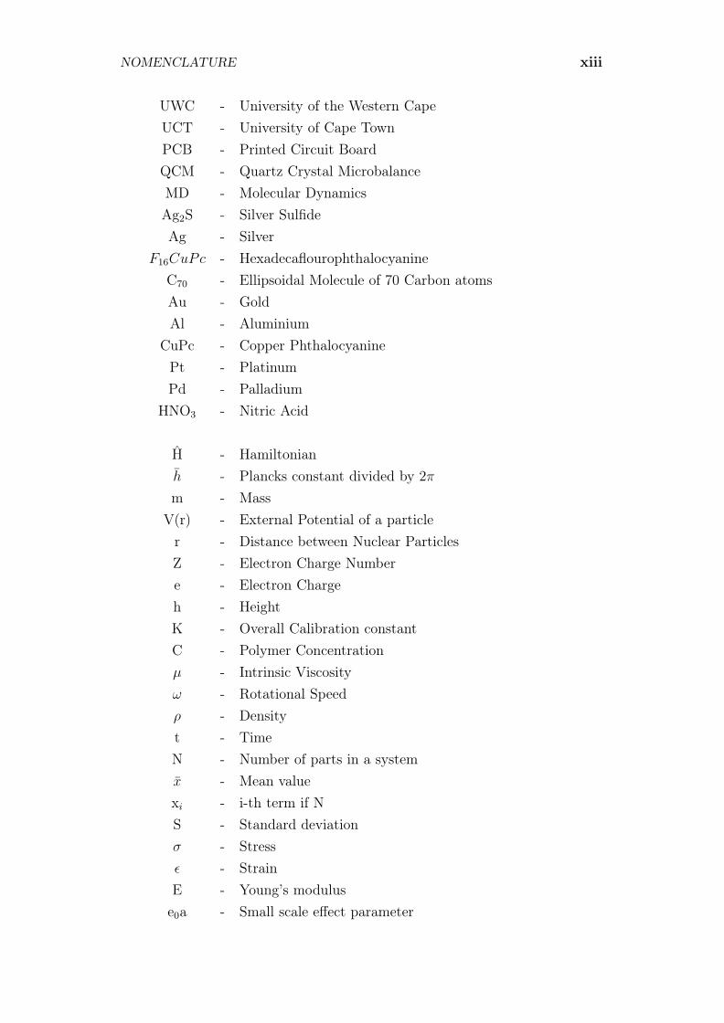
MEMS - Microelectromechanical SystemCMOS - Complementary Metal Oxide SemiconductorNEMS - Nanoelectromechanical SystemASCC - Automatic Sequence Controlled CalculatorDARPA - Defense Advanced Research Projects AgencyAFM - Atomic Force MicroscopeSTM - Scanning Tunneling MicroscopeMFM - Magnetic Force MicroscopeMRI - Magnetic Resonance ImagingSEM - Scanning Electron MicroscopeTEM - Tunnelling Electron MicroscopeUV - Ulrta VioletPLD - Pulse Laser DepositionPLE - Pulse Laser Etching
PMMA - PolymethylmethacrylateITO - Indium Tin OxidePS - PolystyreneCNT - Carbon NanotubeSWNT - Single Wall NanotubePECVD - Plasma Enhanced Chemical Vapour DepositionMWNT - Multi Wall NanotubeDWNT - Double Wall NanotubeDNA - Deoxyribonucleic AcidRF - Radio FrequencyESR - Electron Spin ResonanceXRD - X-Ray DiffractionESD - Electrostatic Discharge
xii
NOMENCLATURE xiii
UWC - University of the Western CapeUCT - University of Cape TownPCB - Printed Circuit BoardQCM - Quartz Crystal MicrobalanceMD - Molecular DynamicsAg2S - Silver SulfideAg - Silver
F16CuPc - HexadecaflourophthalocyanineC70 - Ellipsoidal Molecule of 70 Carbon atomsAu - GoldAl - Aluminium
CuPc - Copper PhthalocyaninePt - PlatinumPd - Palladium
HNO3 - Nitric Acid
H - Hamiltonianh - Plancks constant divided by 2πm - Mass
V(r) - External Potential of a particler - Distance between Nuclear ParticlesZ - Electron Charge Numbere - Electron Chargeh - HeightK - Overall Calibration constantC - Polymer Concentrationµ - Intrinsic Viscosityω - Rotational Speedρ - Densityt - TimeN - Number of parts in a systemx - Mean valuexi - i-th term if NS - Standard deviationσ - Stressε - StrainE - Young’s moduluse0a - Small scale effect parameter

NOMENCLATURE xiv
q - Force working in on a systemQ - Shear force in a structureM - Bending momenty - DisplacementI - Second moment of areaFe - Force due to electrostatic effectsFn - Force due to intermolecular effects
ε0 - Permittivity of a vacuumA - Hamaker’s constantγ - Poisson’s ratiog - Gap distance from Cantilever to basec - Constant speed of light
Tera - 1012
Giga - 109
Mega - 106
Kilo - 103
Milli - 10−3
Micro - 10−6
Nano - 10−9
Angstrom - 10−10
Pico - 10−12
Chapter 1
Introduction
Currently only basic nanodevices can be produced with some degree of con-trol [1]. Microelectromechanical Systems (MEMS) and microsystems made thebreakthrough to commercial products in the 1990’s, adding a well developedunderstanding of Complementary Metal Oxide Semiconductor (CMOS) manu-facturing technology and the experience already garnered from extensive workin the field [2]. At the same time the discovery of the nanotube added tothe interest of the then emerging nanotechnology, and in the dawning of the21st century, commercial sub-micron manufacturing technologies are beingdeveloped, allowing for the steady breakthrough of NanoelectromechanicalSystems (NEMS)
So from the concept of current silicon technology switches and their short-comings, we look at something different, also contrasted with Babbage and hisdifference engine, on top of the growing field of nanotechnology brought to usin practice at the dawn of the 21st century by Richard Feynman in spirit andMaxwell in theory.
Currently technology is falling behind Moore’s law due to size restrictionsand increasing material tolerances. Ten-atom devices are greatly affected by adeviation in doping concentration and interlinks have become bottle neckingstructures. Computing speed thus no longer doubles, with an accompanyinghalving in price, every 1.5 years, as Moore predicted in his later life.
The requirement for faster switching speeds thus necessitates a look atthe available technologies world wide, for switch production and the methodsand techniques available at Stellenbosch University for the fabrication of thesetypes of nanodevices.
1
CHAPTER 1. INTRODUCTION 2
1.1 Research Objectives and Motivation
The objective of this thesis is the of nanomechanical switches and then theirapplication as logic gates. These devices will be designed, simulated and thenmanufactured.
1.2 Report Overview
This report can be broken down into three main parts, namely investigation,manufacture and simulation. In Chapter 2, the broader aspects of the inves-tigation are addressed. It starts with the origins of mechanical calculationand its founder, followed by a discussion of nanotechnology and its subsidiaryconsiderations.
In Chapter 3 nanomechanical switching and current nanomechanical switchesare investigated and discussed. Particular attention is given to the drivingprincipal of the devices, as well as the different applications thereof.
This is followed by a discussion of the procedure and methodology thatwas followed during the course of the project and in writing the report. Thisis done ahead of the manufacturing section in order to ease qualms as to theapproach used in following through with the research.
Chapter 5 discloses the selection process for the manufactured switches aswell as the formulation of the manufacturing methods. Each nanoswitch wasanalysed for possible obstacles to their construction, which were then addressedin full before the attempted production of functional switches.
An attempt was made, in Chapter 6 to simulate the function and failuremechanisms of cantilever style nanodevices, in particular those using carbonnanotubes. This was done because of the extensive use of this type of devicein current micro- and nanoscale devices.
Finally, the results of the report are discussed in the conclusion. Possibleadditions for the laboratory are suggested and improvements to the developeddevices are suggested.

Chapter 2
Literature Study
2.1 Steam powered thinking
In the advances leading to the modern day personal computer, the transistor isheralded as the most fundamental piece, the original building block making thesubsequent evolution of the technology possible. However, before the adventof the solid-state switch, the idea for computing difficult functions with theaid of machines already existed.
If we go to the very beginning of computing there was the abacus from3000 B.C. This was followed by the Scottish mathematician, John Napier’slogarithm sticks from 1594. The logarithm sticks led to the development oflogarithm tables and Napier’s bones. This cylinder spool method of realigninglogarithm tables can be seen in Figure 2.1.
Figure 2.1: A box of Napier’s bones [3]
3
CHAPTER 2. LITERATURE STUDY 4
This inspired the Englishman William Oughttred to invent the slide rule.Although these were the forerunners to the saga of computing, they were stillfar from automated.
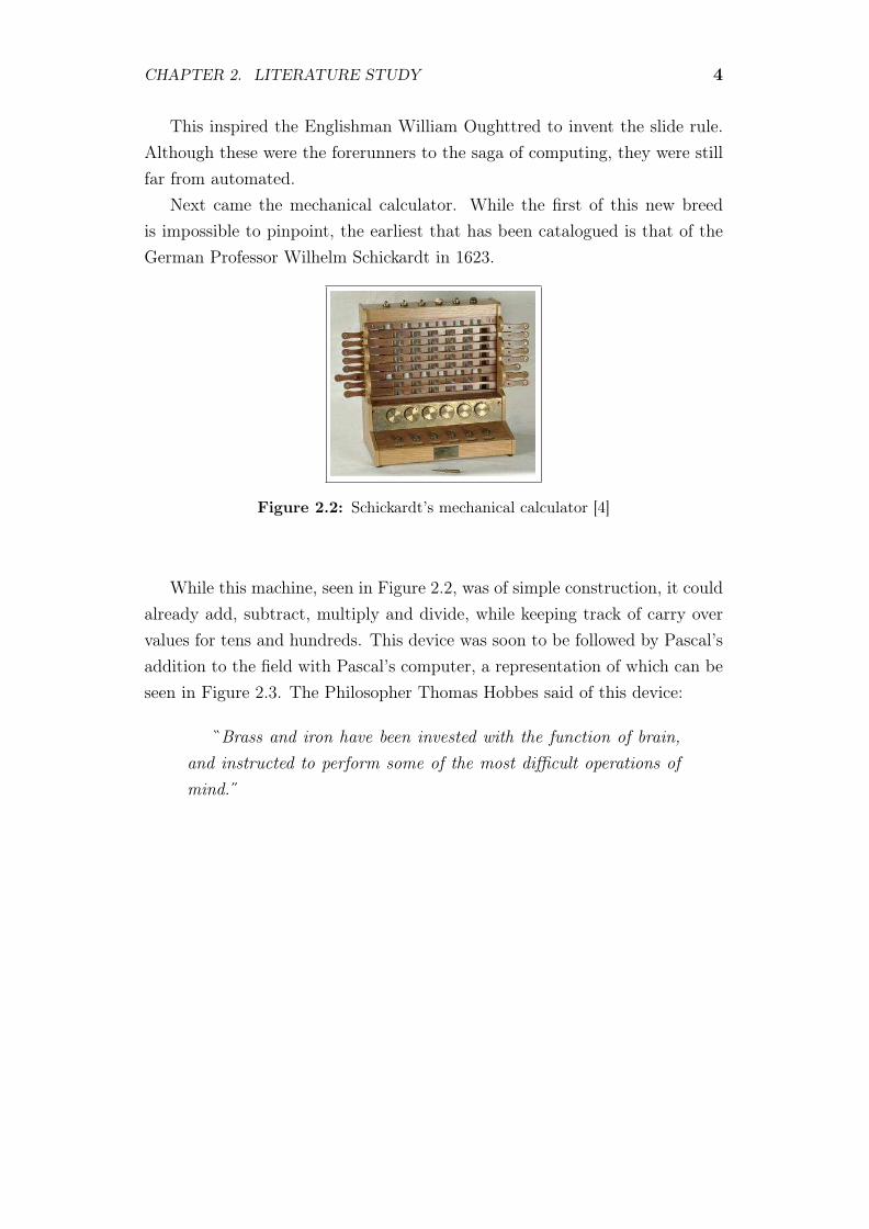
Next came the mechanical calculator. While the first of this new breedis impossible to pinpoint, the earliest that has been catalogued is that of theGerman Professor Wilhelm Schickardt in 1623.
Figure 2.2: Schickardt’s mechanical calculator [4]
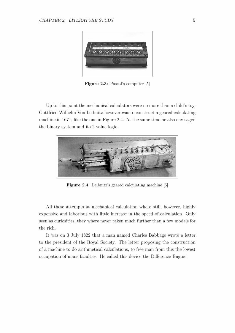
While this machine, seen in Figure 2.2, was of simple construction, it couldalready add, subtract, multiply and divide, while keeping track of carry overvalues for tens and hundreds. This device was soon to be followed by Pascal’saddition to the field with Pascal’s computer, a representation of which can beseen in Figure 2.3. The Philosopher Thomas Hobbes said of this device:
Brass and iron have been invested with the function of brain,and instructed to perform some of the most difficult operations ofmind.˝
CHAPTER 2. LITERATURE STUDY 5
Figure 2.3: Pascal’s computer [5]
Up to this point the mechanical calculators were no more than a child’s toy.Gottfried Wilhelm Von Leibnitz however was to construct a geared calculatingmachine in 1671, like the one in Figure 2.4. At the same time he also envisagedthe binary system and its 2 value logic.
Figure 2.4: Leibnitz’s geared calculating machine [6]
All these attempts at mechanical calculation where still, however, highlyexpensive and laborious with little increase in the speed of calculation. Onlyseen as curiosities, they where never taken much further than a few models forthe rich.
It was on 3 July 1822 that a man named Charles Babbage wrote a letterto the president of the Royal Society. The letter proposing the constructionof a machine to do arithmetical calculations, to free man from this the lowestoccupation of mans faculties. He called this device the Difference Engine.

CHAPTER 2. LITERATURE STUDY 6
Charles Babbage
Figure 2.5: Charles Babbage (1791-1871) [7]
When the English government withdrew from the endeavour of the differenceengine, Babbage was distraught. This also came at the point where Babbagebelieved that he had completed all the necessary refinement and developmentto be able to finish the machine. Babbage said that when someone else finallyconstructs his dream, only then, and that person alone, would be able toappreciate his labour and vision. He believed that it would occur within 50years of his death. It would however be more than 80 years before ProfessorAiken eventually realised the computer.
Even as a child, Charles Babbage was mechanically minded. Having beena sick child and therefore being stuck indoors often, he would disassemble histoys in order to find out how they worked. As he grew up he continued withhis inquisitive pursuits, trying to improve the world around him. One suchevent is rather well documented by others and himself, where he tried to makeshoes that could walk on water. They worked well at first but when the current
CHAPTER 2. LITERATURE STUDY 7
changed deeper into the river he was testing it on, the right shoe gave in. Ittook some time for him to free himself from the grip of his invention and theriver.
The seeds of the difference engine were sown while Babbage was at college.Some sources say that it occurred while he was working with a colleague onstar charts, others say it was during a mathematics lesson. But agree, however,that it was in connection with logarithm tables, which at the time were proneto faults. Having come across another fault in the table he was working withexclaimed:
...wish to God these calculations had been executed with steam!˝
He wanted to produce the tables mechanically, hence excluding the possibilityof calculation and copy errors due to human involvement.
Since the French government had produced such tables by breaking thecalculations down into a series of additive and subtractive operations, Bab-bage thought that a repetitive operating machine would be able to do thesame. Why, he asked himself, would a machine of gears and levers not be ableto replace humans in these tedious low level operations? So he went aboutdesigning a device that would be able to produce accurate tables of squares,roots, cubes, logarithms and the like.
Babbage was undoubtedly far ahead of his time. He proposed a telegraphsystem six years before Morse was to patent the electric telegraph. Flat ratepostage, earthquake detectors and an impromptu submarine, were some of theother things he came up with during the course of his life. But alas, as withmost others who were ahead of their time, he would not be appreciated. Oneof his school time friends said of him, “ . . . not only bad, but who wouldnever get on in the world ”.
CHAPTER 2. LITERATURE STUDY 8
The Difference and Analytic Engines
By 1822 Babbage had developed a pilot model of his difference engine. Thedevice performed so well that the government provided funding for a larger,more expensive, version to be constructed.
While the Difference Engine may have become a success, it was in itsown right already an ambitious undertaking. Babbage, however, had an evengrander vision. He wanted to build a calculating machine that could takeits own calculations and feed them back to itself, and calculate further. Hereferred to it as “ . . . moving forward by biting its own tail ”.
From those ambitions the Analytic Engine was conceived. It was an auto-mated device that could be programmed in advance, having a large numbermemory and was able to print its own tables. The printing was another ofBabbage’s additions in order to eliminate human error from the process ofcalculation and tabulation.
Babbage produced over 200 drawings detailing the approximately 50,000parts that would be needed to make the Analytic Engine. These drawings werethe finest of his time, but all the parts were non-standard sizes and shapes.In addition, they also had tolerances that the technology of his time would behard pressed to achieve.
Even though the Analytic Engine was never finished, the funds providedby the government were more than compensated for by Babbage’s endeavours.The advances in manufacturing processes, machines and production methodsthat came about as a peripheral, bolstered efficiency and productivity. Thefirst steps toward industrial engineering.
Beyond even the economic yield of their investment, the analytic engine wasto assure England’s freedom. The Automatic Sequence Controlled Calculator(ASCC), developed by Professor Aiken, would run around the clock duringWorld War 2. It solved complex problems for the American military, enablingthem to aid England against the Nazi’s.
The Difference Engine worked on the theory that a mathematical equationcould be represented by a table of differences. Take a linear equation such as
y = 3× x
as an example. Every integer of the series will, as shown in Table 2.1, differ

CHAPTER 2. LITERATURE STUDY 9
from the previous by a constant value of 3.
Table 2.1: Differnce Engine Principle
x y Difference1 32 6 33 9 34 12 35 15 3
For a 2nd degree equation this no longer holds true, but the difference ofthe differences is still a constant value. This yields the result of Table 2.2, forthe equation
y = x2.
Table 2.2: Differnce Engine Principle
x y Diff1 Diff21 12 4 33 9 5 24 16 7 25 25 9 2
In this way numerous different mathematical systems may be constructedby using the sequence of cumulative differences through this progression. Sinceit is such a simple principle, Babbage wished to incorporate it in a machine,the construction of which was started in 1821.
The Difference Engine was to perform these operations and tabulate poly-nomial functions. Being revised often, it consisted of 28,000 parts by 1830,and was to be able to calculate with 16 digits and 6 orders. In 1833, however,construction halted after Babbage had a falling out with his head engineer.The machine was never built and the existing 12,000 pieces where smelted

CHAPTER 2. LITERATURE STUDY 10
down. At this point the English government had already spent £17,500 on theendevour, roughly the cost of 20 new steam engines or 2 war ships [8].
The Analytic Engine was conceived in 1834 and bears the closest resem-blance to what we today recognise as a computer. It was programmed usingpunch cards, with separate areas for number storage, iterative results and pro-cessing. It was also capable of several low level programming functions, suchas looping, latching and iteration.
Finally came the Difference Engine Nr 2. Its design was completed in 1849,having started in 1847. This was to be the big one, being more efficient thanthe first Difference Engine and requiring only a third of the parts. It utilisedthe same printing device as the Analytic Engine, which allowed page printingor the printing of a template.
CHAPTER 2. LITERATURE STUDY 11
Babbage today
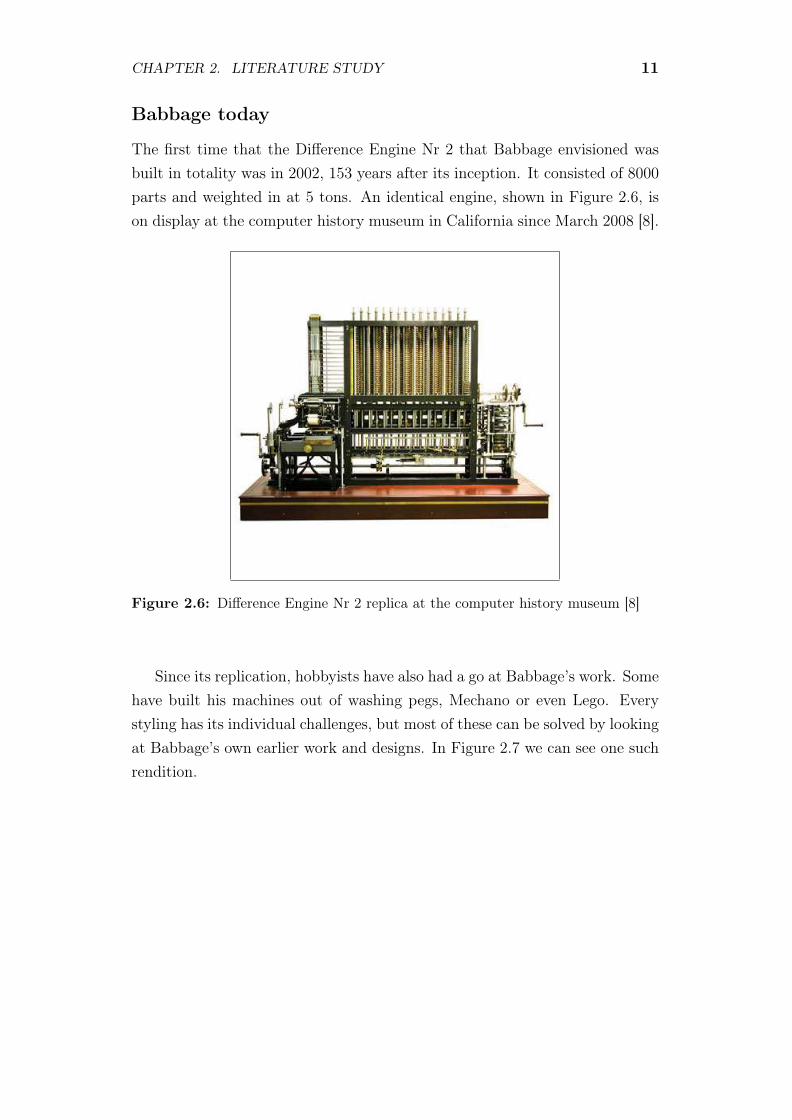
The first time that the Difference Engine Nr 2 that Babbage envisioned wasbuilt in totality was in 2002, 153 years after its inception. It consisted of 8000parts and weighted in at 5 tons. An identical engine, shown in Figure 2.6, ison display at the computer history museum in California since March 2008 [8].
Figure 2.6: Difference Engine Nr 2 replica at the computer history museum [8]
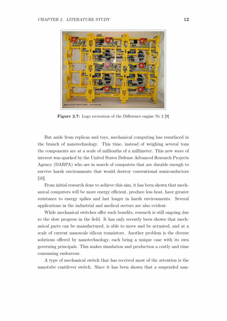
Since its replication, hobbyists have also had a go at Babbage’s work. Somehave built his machines out of washing pegs, Mechano or even Lego. Everystyling has its individual challenges, but most of these can be solved by lookingat Babbage’s own earlier work and designs. In Figure 2.7 we can see one suchrendition.
CHAPTER 2. LITERATURE STUDY 12
Figure 2.7: Lego recreation of the Difference engine Nr 2 [9]
But aside from replicas and toys, mechanical computing has resurfaced inthe branch of nanotechnology. This time, instead of weighing several tonsthe components are at a scale of millionths of a millimeter. This new wave ofinterest was sparked by the United States Defense Advanced Research ProjectsAgency (DARPA) who are in search of computers that are durable enough tosurvive harsh environments that would destroy conventional semiconductors[10].
From initial research done to achieve this aim, it has been shown that mech-anical computers will be more energy efficient, produce less heat, have greaterresistance to energy spikes and last longer in harsh environments. Severalapplications in the industrial and medical sectors are also evident.
While mechanical switches offer such benefits, research is still ongoing dueto the slow progress in the field. It has only recently been shown that mech-anical parts can be manufactured, is able to move and be actuated, and at ascale of current nanoscale silicon transistors. Another problem is the diversesolutions offered by nanotechnology, each being a unique case with its owngoverning principals. This makes simulation and production a costly and timeconsuming endeavour.
A type of mechanical switch that has received most of the attention is thenanotube cantilever switch. Since it has been shown that a suspended nan-

CHAPTER 2. LITERATURE STUDY 13
otube can be deflected using electrostatic forces, several institutions have beenresearching this particular device. Predominantly, they have been attemptingto develop it into a 3 terminal relay.
Although mechanical switches may never reach the speeds of solid statesilicon based technologies, being restricted to 2GHz, research is already goinginto hybrid circuits. If the mechanical switches are used for latching andmemory, the calculations can still be done with CMOS circuits, having a layerof mechanical switches on top of the silicon transistors.

CHAPTER 2. LITERATURE STUDY 14
2.2 Nanotechnology and NEMS
In 1871, a Scottish Physicist named James Clerk Maxwell proposed a thoughtexperiment. In an attempt to disprove the second law of thermodynamics,picture a infinitesimal room with a miniscule entity inside this room. The ex-periment stated that this entity would sort molecules coming through the roominto high energy and low energy groups. The experiment failed to disprove thelaw, but the thought was born.
Nearly a century later the renowned physicist, Richard Feynman, while ata social dinner, broached the topic. He said that no physical law preventedthe building of machinery on the atomic scale. To put it eloquently, there isplenty of room at the bottom. Fifteen years following his statement, the firstnanoscale components where produced.
Nanotechnology is a buzz word that has been tossed around for the lastdecade following the discovery, by scientists, statesmen and Hollywood produc-ers. The definition thrown around by most people amounts to nanotechnologybeing the field of applied science and technology which entails the controlof matter on the molecular scale and the fabrication of devices in that sizerange. While true, it says just enough to propagate uncertainty as to whatnanotechnology really is.
Nanoscience is the study of fundamental principals of molecules and struc-tures in the size range, or having a critical dimension, between 1 and 100nanometres, where unique phenomena allow for novel applications [11]. Nano-technology is the application of these nanostructures into useful nanoscaledevices.
To understand and apply nanotechnology, researchers need to have an un-derstanding of biology, chemistry, physics, engineering and computer science.Depending on the specific application, many other fields may also be necessary,such as protein engineering, surface physics and material science [1].
This being said, it doesn’t seem to explain the large amount of attentionand publicity that nanotechnology has received. To appreciate this, one needsto understand where nanotechnology stands. It has been said that the scale isin the nanometre scale, which while being small, is a unique kind of small.
A nanometre is one millionth of a millimeter, or one billionth of a metre.A human hair is 50,000nm across, a bacterial cell measures a few hundred

CHAPTER 2. LITERATURE STUDY 15
nm across and the latest microchips produced by Intel uses transistors at35nm size. The smallest things visible to the human eye is 10,000nm across[12]. 1nm can accommodate 10 hydrogen atoms or 3 uranium atoms. Anapproximation of the differences in scale can be seen in Figure 2.8, where thebasic nanostructures are shown in comparison to conventional small things andthen to every day items.
Figure 2.8: A visual relation of scales [11]

CHAPTER 2. LITERATURE STUDY 16
Still this does not explain the unique properties of this size range. Let usequate it with the forging of a Japanese katana. The starting material is ironand carbon, forming steel that is folded repeatedly, until it consists of near ona million layers. Now instead of plain hard and light steel, the blade is flexible,even stronger, and sharpens itself with each cut, a change in properties andbehaviour by subdivision.
This is where the crux of the matter is exposed, the nanoscale is wherethe conventional everyday properties of materials like conductivity, hardnessor melting point meet the more exotic properties of the atomic and molecularworld such as wave-particle duality and quantum effects [12]. At nanoscale awire will not obey Ohm’s Law, due to the small scale. The transmission lineis only a few atoms wide, so the electrons are not able to flow as easily, or insome extreme cases need to travel single file.
To emphasise this point let us take a bar of gold with which everyone isfamiliar as an example. The yellow metallic lustre, electric and thermal prop-erties are well documented and used in several capacities. Now, if one wereto cut the bar along each axis, there will be eight golden rhomboids with thesame properties as the original. Cut it the same way again and again, even-tually the dimensions sink into the micrometre range and still the propertiesare the same. Continue cutting again, using specialised equipment, we reachthe nanometre dimensions and suddenly, the properties change. Colour alonemay change to orange, purple, red or greenish, depending on the actual size ofthe gold nanoparticles. This was known by alchemists during the middle ages,and was used to colour the stained glass windows in churches [13].

CHAPTER 2. LITERATURE STUDY 17
Seeing the Infinitesimal
In order to investigate, manufacture and then test nanostructures one mustfirst be able to see and examine structures of that size. Barely being ableto see things of 10,000nm size with the naked eye, a strong microscope willallow the spotting of things at 5nm. But seeing nanostructures as specks isnot conducive to scientific experimentation, so ways needed to be developedto improve imaging techniques.
Some of the methods developed in this capacity are scanning microscopy,spectroscopy, electrochemistry and electron microscopy.
Scanning Probe InstrumentsOne of the first methods to be developed, was the scanning probe devices.Intuitive to us as tactile creatures, this method uses a probe or tip that is slidalong a surface. Imagine it as your finger dragged across a surface, the feel ofthe material already provides information, such as whether it is steel, wood,velvet or tar. Furthermore, the process of moving your finger along the surfacealso gives an impression of the features and topography of the surface.
Fundamental to this method is that the tip be on the same scale as thesurface that is to be scanned, since any profile details smaller than the tip willnot be registered by the probe. Therefore it is common for a scanning probeinstrument’s tip to be honed down to the size of a single atom where it is toscan the target.
In this family the main devices for microscopy are the Atomic Force Micro-scope (AFM), the Scanning Tunnelling Microscope (STM) and the MagneticForce Microscope (MFM) [12].
The AFM uses electronics to measure the force exerted on the probe tipas it moves over the surface. There are two methods or modes that can beused for this measurement, contact or non-contact mode. The contact modeprocedure uses the same method as your finger, by pulling along the surfacewith physical contact. The non-contact mode uses the attractive force betweenthe tip and the surface at close proximity. In Figure 2.9 the measurement andinterpretation cycle of the AFM can be seen.

CHAPTER 2. LITERATURE STUDY 18
Figure 2.9: A visual representation of AFM theory [14]
The STM, as depicted in Figure 2.10, uses a conductive base and platinumtip to pass an electrical current through the sample surface and measure it.Depending on the setup of the system, the STM can either measure the samplegeometry, or measure the local electrical conductive properties. The STM wasthe first of the scanning probe techniques to be developed, earning Gerd Binnigand Heinrich Rohrer the 1986 Nobel Prize.
Figure 2.10: A visual representation of STM theory [15]

CHAPTER 2. LITERATURE STUDY 19
In the MFM the scanning tip is magnetic. As it traverses the surface itsenses the local magnetic structure. It works in a similar way to the readinghead on a hard disk drive or audio cassette player.
With most scanning probe instruments computer enhancement is used toproduce usable images, compiling the linear sets of height, force, current orfield strength measurements into a total picture. Software enhancement is oc-casionally used to reduce noise and distortion on the image.
SpectroscopySpectroscopy refers to shining a light of a specific wavelength on a sample andobserving the absorption, scattering or other properties of the material underthose conditions.
Spectroscopy is the oldest technique, having many applications and forms,offering a variety of insights. Some of these are familiar, like X-rays, wherehigh energy radiation is passed through an object to see how the radiationis scattered by the heavy nuclei of substances like steel or bone. MagneticResonance Imaging (MRI) is another form of spectroscopy.
The difficulty with spectroscopy is that it can only be used to study struc-tures with sizes larger than the wavelength of light being used. Since the wave-lengths of visible light ranges between 400 and 900 nanometres, this doesn’thelp for looking at single nanostructures, but is handy for studying them ingroups [12].
ElectrochemistryElectrochemistry entails the changes in chemical processes by the applicationof an electric current and the generation of electrical currents by chemicalreactions. A common example is voltaic cells, where energy is produced by achemical reaction. The inverse process can be used in electroplating, wherebya metal is made to deposit on an electrically charged surface.
While the method of electrochemistry is widely used to manufacture nano-devices, it can also be used to analyse them. Using electrochemistry, the natureof surface atoms can be measured from the emitted current. More advancedtechniques can be used in conjunction with other microscopy methods to gleanfurther details about a nanostructure [12].

CHAPTER 2. LITERATURE STUDY 20
Electron MicroscopyThe first technique that was used to observe nanostructures was electron mi-croscopy, even before scanning probe microscopy. Instead of using light, likespectroscopy, electron microscopy uses electrons to examine the structure andbehaviour of the devices.
While there are several forms of electron microscopy, they all function onthe principal of accelerating electrons and passing them through the sample.As the electrons encounter nuclei and other electrons, they scatter and bycollecting these scattered electrons, an image can be constructed. This is doneby predicting were the particles where that scattered the collected electrons.
Two examples of these techniques, seen in Figure 2.11, are Scanning Elec-tron Microscopy (SEM) and Transmission Electron Microscopy (TEM). ATEM image can have resolutions sufficient to see individual atoms, but un-fortunately samples must be stained before they can be scanned. Anotherdrawback is that it cannot measure forces or electric fields, but still, it is thebest method for acquiring physical images of nanostructures for analysis andinterpretation [12].
Figure 2.11: Representation of TEM and SEM microscopy [16]
CHAPTER 2. LITERATURE STUDY 21
Simulating Nanodevices
Product and device development used to be exceedingly time and cost in-tensive, due to the necessity of prototypes and physical testing. Thanks tobreakthroughs in computational power and the sciences, most systems can bemathematically modelled and run to obtain results in a faster, cheaper man-ner. While simulation does not eradicate the necessity of physical testing, itdoes speed up the production time, provide comparable results and lessen thenumber of prototypes needed considerably.
One of the first implementations of computational simulation was duringthe Second World War, involving the behaviour of neutrons. To set up andrun the experiment over and over again with the possibility of collisions wasarduous, time consuming and very expensive. Since the basic principals of thereactions were known, mathematicians where consulted and a model drawn up.The system that was set up was able to predict the outcome of the neutronreactions with remarkable accuracy. After the war many new technologies werebeing developed or adapted, providing ample opportunity for the expansion ofsimulation.
However in order to simulate the system the basic principles behind theprocesses incumbent on that system need to be understood. For somethinglike a bending beam, classical mechanical theory has an empirical solution.So, given the material, physical dimensions and applied load, the curve of thebeam, deflection along its length and even failure can be predicted.
With nanotechnology, however, the interaction between atoms in smallerdevices moves the ball from the mechanical theory court into the domain ofquantum theory, the science of all things infinitesimal. Having large, by com-parison, devices with atomic scale components mean that the governing equa-tions need to contain elements of both mechanical and quantum theory. Sincethe two theories tend to be contradictory [17], compromises are inevitable.
Nanotechnology makes design a crucial part of the development process,since, with the right knowledge, the same goal can be achieved in any numberof ways, limited only by the imagination. In this world where the question haschanged from What can we do?˝to What do we want to do?˝, simulationhas become important for the evaluation of these products.
The many particle system problems of nanotechnology have found fourtypes of numerical solutions, namely quantum theoretical calculation (or ab

CHAPTER 2. LITERATURE STUDY 22
initio), molecular mechanics, Monte Carlo and molecular dynamics.The ab initio techniques commonly use self-consistent field methods, linear
combinations of atomic orbitals or the density functional method [1]. Thesetechniques all have to do with molecule to molecule gravity and potentialsin respect to all other particles in the system. If one takes a look at theHamiltonian, an operator pertaining to the total energy of a system (2.1), ofa system containing N particles of masses mi we see the possible problems.
H =∑
[− h2
2mi
52i +Vi(ri)] +
∑Vik(ri, rk) (2.1)
Vik(ri, rk) =ZiZke
2
(rk − ri)(2.2)
A system’s complexity will determine the length of the simulation, becausean increase in particles results in a exponential increase in calculations. In asimple 100 argon atom system, a summation of 1011400 volume elements wouldbe required to reach a solution [1].
Due to this exponential increase in calculations, ab initio techniques revolvearound simplifications and assumptions made for individual cases, in order tominimise the computational intensity of its equations.
Molecular mechanics uses the approximation of chemistry models wherea molecule is simulated using balls and sticks. The balls are atoms and thebonds between them is represented by the sticks connecting them. The aimof this method is to find stable configurations for the system out of its poten-tial energy, in other words finding the minimum energy considering the bondtension, bending, torsion, Van der Waal’s and Coulomb interactions [18].
For this method to work effectively the initial conditions need to be fairlyclose to equilibrium for a convergent answer. An improvement on this systemis the molecular dynamics method that uses similar approximations, but solvesfor the system using Newton’s equations of motion. This allows the change inthe system to be modelled over discrete time steps where the total informationis available [1].
The molecular mechanics and mechanics methods are both mechanicalmodels however, and as such cannot include the effects of quantum interactionsin the system. Systems modelled using these methods must be approachedwith an understanding of the quantum effects on the system, keeping in mind

CHAPTER 2. LITERATURE STUDY 23
how they may cause differences in the result.Finally, there is the Monte Carlo method that uses sampled data from the
system and time steps statistically determined by a Boltzmann distribution.The Monte Carlo method evaluates the system with various random values andis particularly useful for systems that are nonlinear, complex or have coupledvariable parameters.
Each of these methods have their own strengths and limitations, dependingon the assumptions made and computational methods used. Here the besttechnique becomes the one whose assumptions are nearest to the implementedsystem. The mechanical models do not account for quantum effects, causinglimited precision and validity. However, they are able to handle large systemsbetter. The quantum theoretical method is highly accurate, but becomeslaborious for larger systems. The Monte Carlo method needs to be tailored foreach configuration with respect to the time steps used, and the data requiredcan be hard to obtain for the simulation [1].

CHAPTER 2. LITERATURE STUDY 24
Manufacturing of NEMS
Many breakthroughs have been made at a rapid rate over the last few years, butthey have yet to make the transition into technology. This can be attributed tohindrances in the manufacturing of nanodevices. For example, while shrinkingdimensions may hold the answer to memory requirements, this cannot, how-ever, be implemented without a way to connect the individual bits, a processthat would require the connection of wire billions of nanodevices.
Most research is focused on manufacturing and manipulating a few, toseveral hundred particles or molecules into the required setup. In order tocommercialise the technology, the aim changes to being able to replicate theconfigurations and devices into large production volume synthesis techniques,while having a robust and reliable process. After producing the devices, waysmust be found to incorporate them in microstructures, larger systems and thena finished product [13].
There are two main approaches to the fabrication of nanostructures anddevices. The first is the Top-Down approach, which uses larger machines toform smaller devices similar to cutting a structure from a larger chunk ofmaterial. The second is the Bottom-Up approach, where the device is puttogether from smaller parts, like a house is built of bricks.
The solution for commercial fabrication is believed to be a combination ofthese two approaches, cutting out of the main structure, adding in the morecomplicated devices, and then grow them together.
Nanoscale LithographyLithography comes from the Greek word lithos, meaning stone and grapienmeaning to write, referring to the process of inking a stone and transferringthe image to paper.
This later evolved into photolithography, a process by which a mask onglass is transferred to thin photosensitive films by means of a Ultraviolet (UV)light. This process has little tolerance for non-planar topography, hence beingan exclusively two-dimensional process [19].
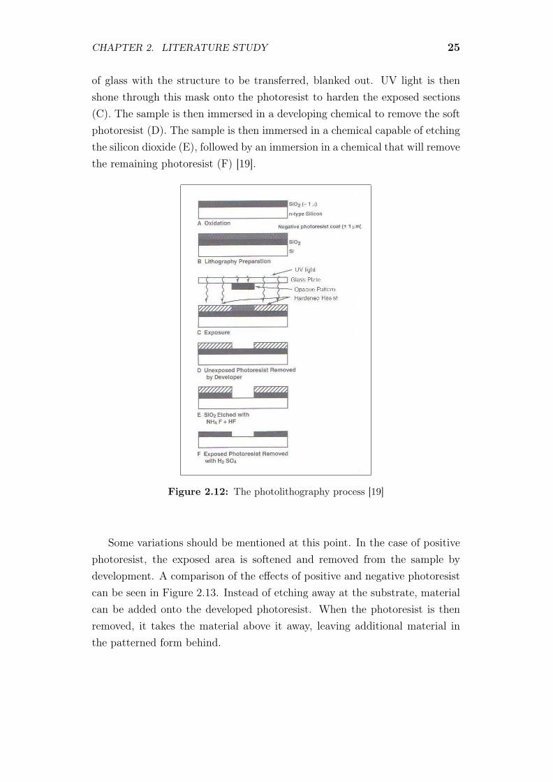
The photolithographic process will be explained using an oxidised siliconwafer and negative photoresist as an example. See Figure 2.12 for the stepby step guide. After cleansing the silicon wafer with acetone, it is coatedwith negative photoresist and baked (B). The sample is placed below a piece
CHAPTER 2. LITERATURE STUDY 25
of glass with the structure to be transferred, blanked out. UV light is thenshone through this mask onto the photoresist to harden the exposed sections(C). The sample is then immersed in a developing chemical to remove the softphotoresist (D). The sample is then immersed in a chemical capable of etchingthe silicon dioxide (E), followed by an immersion in a chemical that will removethe remaining photoresist (F) [19].
Figure 2.12: The photolithography process [19]
Some variations should be mentioned at this point. In the case of positivephotoresist, the exposed area is softened and removed from the sample bydevelopment. A comparison of the effects of positive and negative photoresistcan be seen in Figure 2.13. Instead of etching away at the substrate, materialcan be added onto the developed photoresist. When the photoresist is thenremoved, it takes the material above it away, leaving additional material inthe patterned form behind.

CHAPTER 2. LITERATURE STUDY 26
Figure 2.13: The effects of positive and negative photoresist [19]
As the dimensions of a structure shrink, however, the chemicals neededto make the film and the method of developing the resist has to adapt. Theresist, exposure and etching techniques change, but the principle remains thesame. A few of the techniques developed to overcome the scale barrier are nowdiscuss.
Dip Pen NanolithographyThis is a rather direct way to put structures onto a substrate by writing onit, as one would write with ink or in wax. In both cases a pen is needed, fineenough to make nanoscale markings, which an AFM tip is ideal for.
In the first instance, a reservoir of atoms or molecules is kept on the probe,and as the tip moves, these particles are manipulated down the tip and ontothe surface, as in Figure 2.14. Where the tip thus moves, the lines and patternsare left behind, like an old fashioned dip pen, hence the name.

CHAPTER 2. LITERATURE STUDY 27
Figure 2.14: Dip pen nanolithography setup [13]
In the second instance, the sample is coated with photoresist beforehandand the AFM tip is used to remove the pattern. Alternatively, the sample maybe coated with the desired material and the excess scratched away to revealthe pattern.
Of this method’s many advantages, two should be highlighted. Most im-portantly, nearly anything can be used as nano-ink and almost any surfacecan be written on. The other great advantage is that detailed and complexpatterns can be created since an AFM tip is easy to control and manipulate.The drawback of this method, however, is that it is slow and not conducive tomass production [12].
E-Beam LithographyAs was mentioned before, the large wavelengths of visible light are not ableto produce the small features required for nanodevices. A solution might beto use smaller wavelengths of light, but this has the side-effect of introducinglarge quantities of energy, that may harm the surface and structure that isbeing worked on.
So instead, like with spectroscopy and electron microscopy, light is replacedwith electrons. This electron beam may be employed to etch away material athigh power levels, or to cut away photoresist. It is also possible to push loosenanostructures around on the surface with the E-beam method.

CHAPTER 2. LITERATURE STUDY 28
Nanosphere Liftoff LithographyIn the early days of printing, the dot matrix method was used, where letterswhere made up of a series of ink dots. Similarly, working at nanoscale, materialdots or spheres can be put down and used as a blank. At its most extreme,individual molecules can be used as the mask. In an array of spheres, whereeach sphere is surrounded by 6 others, the deposition of material will puttriangular structures with concave sides onto the surface.
The benefits of this technique is that multiple layers can be put down se-quentially. There are a variety of materials that can be used as the mask anddeposition material alike. This method is also an exclusively linear method,building upwards without the need for etching, and for commercial or highdefinition application, millions of the triangular dots can be made simultane-ously [12].
Self-AssemblySelf-assembly deals with the way things in nature come about under their owninitiative. In nature nothing needs to be built, they form and grow on theirown. Most other fabrication techniques require a lot of time, effort and energyto produce a result, and researchers began to wonder if they might not be ableto tap into nature’s secret for having things build themselves.
Many disciplines have used this concept, and each has its own descrip-tion of what self-assembly means. Taking a general view of this field, onecan say that self-assembly pertains to the spontaneous formation of organisedstructures through a stochastic process that involves pre-existing components,is reversible and can be controlled by proper design of the components, theenvironment and the driving force [20].
To help picture this concept, think of a memory alloy like nitinol wire. If thewire is shaped into a structure, for simplicity say a square, and heated, it setsinto this form for high energy states. Once cooled the wire can be straightenedto its original shape, however, now when it is heated it will return to the squareshape that it was formed to during the heating phase.
A common method of employing self-assembly would be to introduce aunique atom or molecule to an existing nanostructure. What makes this par-ticle unique is that, in combination with the nanostructure, they attempt tomove to a lower state of energy, changing position and forming bonds [12].

CHAPTER 2. LITERATURE STUDY 29
Large structures can be formed in this way, without the attention and consis-tent input required by some other methods.
The advent of nanotechnology has given self-assembly a big push to theforefront, since nanodevices of only several thousand atoms are highly relianton the position of some of these particles. Now the addition of another atomor molecule can have a large effect on the overall structure, or functionality ofsuch a device.
In Figure 2.15 an example of current self-assembly can be seen. This isan endeavour by Massachusetts Institute of Technology (MIT) to make easilyassembled nano-motors, capacitors and memory elements. This technique isreferred to as nano-origami, moving planes relative to one another by enablingthe folds [21].
Figure 2.15: Self assembled polymer sheet [21]
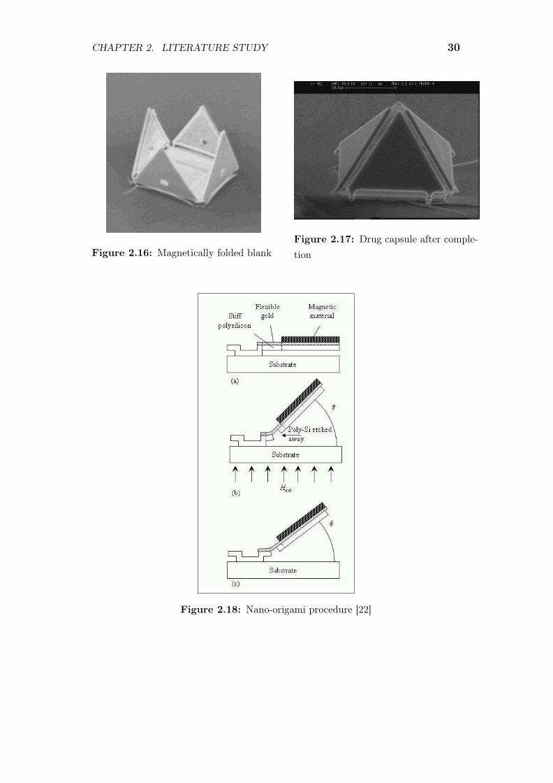
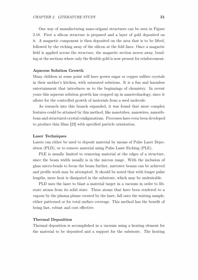
At the Information Sciences Institute a similar project has been undertakento improve drug delivery systems. A package is self assembled from polysiliconto carry the drug into the body and transport it to the relevant areas. Figure2.16 shows the capsule before being closed and Figure 2.17 shows the completeproduct.
CHAPTER 2. LITERATURE STUDY 30
Figure 2.16: Magnetically folded blankFigure 2.17: Drug capsule after comple-tion
Figure 2.18: Nano-origami procedure [22]
CHAPTER 2. LITERATURE STUDY 31
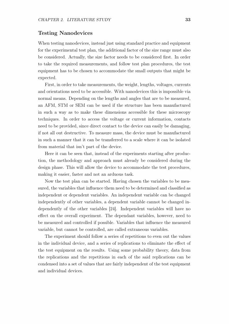
One way of manufacturing nano-origami structures can be seen in Figure2.18. First a silicon structure is prepared and a layer of gold deposited onit. A magnetic component is then deposited on the area that is to be lifted,followed by the etching away of the silicon at the fold lines. Once a magneticfield is applied across the structure, the magnetic section moves away, bend-ing at the sections where only the flexible gold is now present for reinforcement.
Aqueous Solution GrowthMany children at some point will have grown sugar or copper sulfate crystalsin their mother’s kitchen, with saturated solutions. It is a fun and harmlessentertainment that introduces us to the beginnings of chemistry. In recentyears this aqueous solution growth has cropped up in nanotechnology, since itallows for the controlled growth of materials from a seed molecule.
As research into this branch expanded, it was found that more complexfeatures could be attained by this method, like nanotubes, nanowires, nanorib-bons and structured crystal configurations. Processes have even been developedto produce thin films [23] with specified particle orientation.
Laser TechniquesLasers can either be used to deposit material by means of Pulse Laser Depo-sition (PLD), or to remove material using Pulse Laser Etching (PLE).
PLE is usually limited to removing material at the edges of a structure,since the beam width usually is in the micron range. With the inclusion ofglass micro-beads to focus the beam further, narrower beams can be achievedand profile work may be attempted. It should be noted that with longer pulselengths, more heat is dissipated in the substrate, which may be undesirable.
PLD uses the laser to blast a material target in a vacuum in order to lib-erate atoms from its solid state. These atoms that have been rendered to avapour by the plasma plume created by the laser, fall onto the waiting sample,either patterned or for total surface coverage. This method has the benefit ofbeing fast, robust and cost effective.
Thermal DepositionThermal deposition is accomplished in a vacuum using a heating element forthe material to be deposited and a support for the substrate. The heating

CHAPTER 2. LITERATURE STUDY 32
element can be a wire or crucible made from tungsten, stainless steel, molyb-denum or inconel, depending on the material that is to be deposited.
The system is placed under vacuum and the deposition material is heatedto its sublimation temperature, while being shielded from the sample by ascreen. When the sublimation temperature is reached, the screen is removedand the sublimated material steadily deposits on the substrate.
While this process takes a long time, it yields high quality films, and thesystem can be modified in a variety of ways to make for a versatile and robustdeposition method.
Sputter DepositionSimilar to the PLD technique, material is liberated from a target to be de-posited on the substrate. The difference is that the plasma is not produced bya laser, but rather by high current application in a gas environment (usuallyargon) and the vapour isn’t allowed to float down on its own, instead beingpropelled towards the substrate due to an applied electric field.
Like PLD this method is part of the physical vapour deposition family,hence the similarity. Also the film is of similar quality, but the depositiontakes considerably longer, especially if the substrate needs to be heated.
CHAPTER 2. LITERATURE STUDY 33
Testing Nanodevices
When testing nanodevices, instead just using standard practice and equipmentfor the experimental test plan, the additional factor of the size range must alsobe considered. Actually, the size factor needs to be considered first. In orderto take the required measurements, and follow test plan procedures, the testequipment has to be chosen to accommodate the small outputs that might beexpected.
First, in order to take measurements, the weight, lengths, voltages, currentsand orientations need to be accessible. With nanodevices this is impossible vianormal means. Depending on the lengths and angles that are to be measured,an AFM, STM or SEM can be used if the structure has been manufacturedin such a way as to make these dimensions accessible for these microscopytechniques. In order to access the voltage or current information, contactsneed to be provided, since direct contact to the device can easily be damaging,if not all out destructive. To measure mass, the device must be manufacturedin such a manner that it can be transferred to a scale where it can be isolatedfrom material that isn’t part of the device.
Here it can be seen that, instead of the experiments starting after produc-tion, the methodology and approach must already be considered during thedesign phase. This will allow the device to accommodate the test procedures,making it easier, faster and not an arduous task.
Now the test plan can be started. Having chosen the variables to be mea-sured, the variables that influence them need to be determined and classified asindependent or dependent variables. An independent variable can be changedindependently of other variables, a dependent variable cannot be changed in-dependently of the other variables [24]. Independent variables will have noeffect on the overall experiment. The dependant variables, however, need tobe measured and controlled if possible. Variables that influence the measuredvariable, but cannot be controlled, are called extraneous variables.
The experiment should follow a series of repetitions to even out the valuesin the individual device, and a series of replications to eliminate the effect ofthe test equipment on the results. Using some probability theory, data fromthe replications and the repetitions in each of the said replications can becondensed into a set of values that are fairly independent of the test equipmentand individual devices.

CHAPTER 2. LITERATURE STUDY 34
Now we consider the effect of a nanoscale device on the test equipment. Thevalues to be measured may be very small. Currents in the pico-amperes andmasses in the micro-grams are not unusual. Equipment suited for these kindsof measurements must thus be used. The range, resolution and accuracy of theequipment must also be taken into account [24]. Manufacturers usually includea section in the manual where they state the possible linearity, hysteresis,sensitivity and zero shift errors that may be encountered while using theirequipment.

CHAPTER 2. LITERATURE STUDY 35
2.3 To summarise
The pioneers of each of the mentioned fields were legends of their time and thefields that they opened for us have revolutionised the way things were doneduring their age. We must now try to combine these contributions in order tomove even further along the path.
The discoveries of nanotechnology bring the scientific disciplines ever closertogether, into a collusive whole. 2400 years after Aristotle formed the disci-plines of science [25], we can reform them, with the same logic he taught us.
Using nanotechnology to miniaturise Babbage’s engines would open up anew field of possibilities in what used to be impossible areas, producing tinysystems of near infinite complexity.
Yet in order to do so, the starting point is the small of the small. Manu-facturing the components and producing mechanical switches in the nanoscalethat will rival their solid state counterparts.
At a surprising rate, however, researchers have stepped up and are pro-ducing ever more ingenious and varied solutions to these first stumblings intonanomechanical switching. Much promise is being show in this field and fol-lowed up with a remarkable vigour.

Chapter 3
Mechanical Nanoswitches
A lot of effort has gone into researching alternatives to modern day silicontechnology for switching purposes. The trouble is being able to go ever smaller,while remaining reliable and maintaining high levels of power.
3.1 Device overview
MEMS switches where lucrative as a replacement for conventional relays andsolid state switches due to their size and speed advantages. Also, they do notsuffer as much from on-resistance and parasitic capacitance [13].
NEMS promise to offer an increase in these benefits. Apart from the op-erational benefits, they increase the available avenues of implementation andapplication.
Switch activation is largely achieved using electrostatic and magnetic means.In this chapter several types of switches will be investigated, some using elec-trostatic switching, but predominantly alternative switching techniques will besought, as led by current research or particularly promising avenues of research.
Since it is mechanical switches which are going to be researched, it shouldbe remembered that part of the power going into the switch is being used tomaintain contact in either the on- or off-state. This force is the remainder anddiffers from what is needed to close the switch This small force is a major factorinfluencing the area and quality of the contact. Another issue is that this forcecannot be made too large, because it may result in negative consequences,lastly and in the worst case, device failure.
36

CHAPTER 3. MECHANICAL NANOSWITCHES 37
3.2 Silver Sulfide Switches
A recent eureka moment led to the exploitation of the unique conductive prop-erties of silver sulfide. While scanning a silver sulfide surface with a STM, theresearchers discovered that little mounds of silver were forming on the surfaceof the sample [26]. Further study showed that the silver mounds where formeddue to the proximity of the electrified platinum tip and grounded sample.
Silver sulfide (Ag2S) is an ionic conductor, meaning that in its crystal latticeions may assume many possibly positions, allowing them to move around freely.More so, it exhibits these properties at room temperature. Another materialthat shares these properties is copper sulfide.
When one layers silver sulfide between two silver layers, as in Figure 3.1,and the silver electrodes are connected to a battery, the effect of this ionicconduction can be observed. At the positive electrode, Ag+ ions are formedat the Ag-Ag2S interface, while at the negative electrode interface Ag+ ionsare reduced [26].
Figure 3.1: Silver sulfide as an ionic conductor [26]
This provided a material that could, at room temperature, conduct ions(allowing material transfer), conduct electrons (allowing current transfer) andactuated by a low voltage. A device was then developed that would use theseproperties to make a switch that grows its contact in a reversible manner.

CHAPTER 3. MECHANICAL NANOSWITCHES 38
While many switching mechanisms have been reported between STM tipsand substrates in recent years, these required an STM to function, whereasthe silver sulfide only needs a reversible power source and small contact area.With this in mind, Terabe et al. [27] were able to come up with a cunningsolution. A layer of Ag2S on top of a silver wire is in contact with a thickplatinum wire through a 1nm thick silver layer.
Figure 3.2: Silver sulfide switch model [26]
A voltage is then applied over the platinum and silver terminals . Whencurrent flows from the platinum to the silver, as in Figure 3.2a, Ag+ ions aretransported into the Ag2S causing the silver layer to vanish, breaking contactand putting the devise in the "off" state. When the current flows from thesilver to the platinum contact, as in Figure 3.2b, localised connections formfrom the silver sulfide to platinum, as Ag+ ions grow back out putting the

CHAPTER 3. MECHANICAL NANOSWITCHES 39
device into the "on" state. This process is reversible and very rapid, sinceonly a few atoms are involved [26]. In Figure 3.3, the full switching process isdepicted in a particle model.
Figure 3.3: Silver sulfide reversible particle model [27]
Since a voltage higher than 100mV is required to change states, the stateof a device can be read non-destructively at voltages below this. This makesmemory, as well as switching applications, ideal for this type of device.

CHAPTER 3. MECHANICAL NANOSWITCHES 40
3.3 Photoswitches
Photons seem poised to take over from electrons as demand for high stor-age density and fast data-processing rates increase. As such, many approacheshave been used to develop binary switches, memory and logic devices. Some ofthe promising materials in the field are zinc oxide nanotubes, polymer-coatedcarbon nanotubes, spiropyrans and doped polymethylmethacrylate (PMMA),although most of them exhibit low on/off ratios and high light intensity re-quirements. A high on/off ratio and low light intensity requirements will becritical for future optoelectronic devices [28].
Photonic devices using organic semiconductors and insulators are becomingincreasingly popular, due to their advantages over their inorganic counterparts.Some of these are lower cost, flexibility and large area application [29].
Phototransistors have been developed to improve the sensitivity and noisevalues of simple photodiodes. Following their development, attempts have beenmade to incorporate organic semiconductors to improve the device functional-ity. One case study, using hexadecaflourophthalocyanine (F16CuPc), showedparticular promise in its stability and self organising properties.
Figure 3.4: Schematic and topographic views of a phototransistor [29]
A single-crystalline ribbon of F16CuPc is used as the functional compo-nent, as shown in Figure 3.4. Under bombardment with light of a photonicenergy equal or higher than the materials bandgap energy, charge carriers areliberated [29], which is depicted in Figure 3.5. In the absence of a gate elec-trode the device operates directly as a photoswitch. While the on/off ratioof the photoswitch, roughly 100Hz, is two to three orders of magnitude lower

CHAPTER 3. MECHANICAL NANOSWITCHES 41
than that of the phototransistor, it removes the addition of the gate electrode,which is a difficult task due to the nanoscale alignments required.
Figure 3.5: Model of a F16CuPc photoswitch [29]
In electrically bistable devices of the form metal/organic insulator/metal,as in Figure 3.6, the switching phenomenon is due to metal filament penetra-tion through the organic insulator. Xinjun Xu et al. investigated the possibilityof a photo response in these devices [28].
Figure 3.6: Functional model of the organic insulator photoswitch [28]
CHAPTER 3. MECHANICAL NANOSWITCHES 42
The initial device specifications where Indium Tin Oxide (ITO) coated glassused as the substrate and bottom contact, polystyrene (PS) as organic insu-lator and gold as the top metal contact. Three different material thicknesseswere tested, as well as other organic insulators, most prominently PMMA. Thetop metal contact was also exchanged for aluminium during some tests.
The devices worked admirably. Below a threshold voltage determined bydevice geometry, the device switches reliably between the on and off states,once a calibration run is made. The calibration run consists of a prolongedUV exposure to push the metal filaments through the organic insulator.
The role of the radiation pressure, provided by the photons can be ex-plained as follows. After activation, the metal filaments are formed in theorganic insulator, some of which are then very close to the ITO. Due to theorganic insulator being very thin, large currents caused by tunnelling occurwhen voltage is applied. This is then referred to as the on state. When thedevice is then exposed to UV radiation, the metal filaments are pushed backfrom the ITO causing greater distance to lessen the current flow. The deviceis now in the off state. When the UV radiation is then removed, filamentstretching due to the electric field force brings the filaments closer to the ITOagain, causing current recovery [28]. On/off ratios in the order of 106 wereachieved.
Nanofibers have been undergoing a lot of research in the area of light gen-eration and further applications, specifically on device light sources. Thisresearch has shown a myriad of applications for organic nanofibers, such asthe already named light sources, detectors, sensors and also switches.
Once the fibers have been deposited on the substrate, the state of the hostpolymer can be altered from the transparent state (off) to a coloured/opaquestate (on) using UV light. The reverse can be achieved using green light.Like the nano-ribbon photoswitches these polymer fiber switches also presenta switching ratio of around 100Hz [30].

CHAPTER 3. MECHANICAL NANOSWITCHES 43
3.4 Carbon Nanotube Switches
The Carbon nanotube (CNTs) was the second fundamental nano building blockto be discovered. The first was the buckminsterfullerene, or buckyball, whichwas discovered in 1985, six years before the carbon nanotube.
Since being able to look at, grow and manipulate them reliably, carbonnanotubes have formed the basis of many nanodevices. This is due to itswell characterized chemical and physical structures, low mass and dimensions,exceptional directional stiffness and range of electrical properties [31]. Sin-gle Wall Nanotubes (SWNT’s) have even shown changes in their electronicproperties depending on its interaction with the environment [2].
Traditional methods of manufacturing carbon nanotubes are arc discharge,laser ablation, thermal synthesis and Plasma Enhanced Chemical Vapour De-position (PECVD) [32], followed by a gleaning procedure to attain the nan-otubes of appropriate chirality, size and length.
Due to the human tendencies towards following what they know, the firstset of CNT nanoswitches resemble press switches, much like a telegraph tapswitch. Figure 3.7 shows such a device. A nanotube is made to hang overthe silicon dioxide substrate from a substrate silicon pillar, much like a singleside supported cantilever. Two metal contacts are present under the nanotubeand a layer of metal is deposited onto the pillar, to serve as a contact to thenanotube.
Figure 3.7: Representation and SEM image of a basic CNT switch [31]
The inner of the two substrate terminals is defined as the gate and theouter terminal is the drain, while the conducting tip of the pillar is the source.When charge is induced in the nanotube by applying a voltage to the gateelectrode, the resulting capacitive force between them causes the nanotube to

CHAPTER 3. MECHANICAL NANOSWITCHES 44
bend. Once the nanotube has bent far enough, it contacts the drain, complet-ing the electrical contact [31].
Another nanotube switch, using the same principle with a bit of a twistis the double supported cantilever design, as in Figure 3.8. The nanotube isplaced over a trench like a bridge over a trench, at the bottom of which is aconductive material. This bottom region serves as a puller when a voltage isapplied, since the induced charge in the nanotube and the resulting capacitiveforce forces the nanotube to deflect, to form a bend in the structure.
Figure 3.8: Model of the CNT trench switch [33]
This bending restricts electron tunnelling between the two sides of thetrench through the nanotube. When the applied voltage is removed, the nan-otube corrects itself and standard electron flow resumes. There are labs thathave reported switching speeds of up to 1MHz using this technique.
The novel linear bearing nanoswitches also uses a CNT suspended overa trench, only this time the nanotube is severed by ramping the current tillthe nanotube breaks down, forming a gap in the bridge. Now in the caseof Multi-walled nanotubes (MWNT) and Double-walled Nanotubes (DWNT)this leaves two sides, each with concentric nanotubes. Taking advantage ofthe low intershell friction the inner nanotubes can be actuated to telescopeout of the outer shell using electrostatic forces [34]. When the two sides meet,electrical contact is restored. By introducing a gate in the DWNT device, theprocess can be reversed repeatably.

CHAPTER 3. MECHANICAL NANOSWITCHES 45
Figure 3.9: Model of the telescoping nanoswitch and representation of the break-down gaps [34]
One of the major advantages of this switch is that the contacts are selfaligning. After the nanotube is placed, or grown in place, all the ensuing stepsrequire no additional mechanical work.
One of the more unique switching solutions is the placing of a C70 moleculebetween two CNTs with open ends. The configuration is depicted in Figure3.10.
Figure 3.10: C70 Switch model [35]
The C70 is an interesting molecule due to its particular electrical and ther-mal properties, as well as its large energy bandgap, however, much is left toinvestigate of its properties. Here however, the highly directional nature ofits molecular structure is used. At 60 intervals the molecule has distinct re-peating features that are conducive to electron flow, and alternative betweenthese points the flow decreases. A change of current in the region of 3 ordersof magnitude is experienced between the on/off states.

CHAPTER 3. MECHANICAL NANOSWITCHES 46
3.5 Organically Actuated Switches
One of the main impedances to the evolution of NEMS beyond static anddynamic nanostructures to fully fledged molecular machinery, is the lack ofnanoscale actuators, such as linear and cyclic motors, pumps and turbines.There have been many discoveries pertaining to actuators, some very promis-ing, but they tend to be difficult to position.
An example of this is the droplet nanomotor developed by scientists atBerkeley. It consists of 2 spheres of liquid metal, one large and one small, ascan be seen in Figure 3.11. They are placed on a carbon nanotube throughwhich an electric current is allowed to flow. This forces atoms to migrate fromthe larger sphere to the smaller one. Once the smaller sphere is large enoughto touch the other one, difference in surface tension causes atom migration tothe larger sphere, restoring the earlier state. On its scale it gives about 100million times the power output of a V6 225 horsepower engine [36].
Figure 3.11: Nanomotor from liquid spheres [36]
Once again, for a simple efficient solution we turn to nature. Evolution haslong since created means of actuation at a small scale. In this particular case,Deoxyribonucleic Acid (DNA) strands and muscle tissue.

CHAPTER 3. MECHANICAL NANOSWITCHES 47
Organic bistable compounds hold particular promise in regards to artificialmolecular actuation. Two specific examples are DNA molecules that walk androtaxanes that contract, both when exposed to ionised fluid.
The DNA motion can be used to move loose connection blocks to form aclosed circuit. An organic walking path is deposited and the connector is placeon this track with DNA legs deposited on its underside. A SEM image of sucha configuration can be seen in Figure 3.12. The rotaxane can be placed ontocantilevers and bend them when contacted.
Figure 3.12: Organically actuated contact switch [13]
The force generated in the rotaxane molecule is approximately 40pN. Alonga bar of 1 µm, this equates to a total deflection of 45nm.

CHAPTER 3. MECHANICAL NANOSWITCHES 48
3.6 To Summarise
In this chapter, a brief overview of current mechanical nanoswitches was given.First, it was explained why NEMS are being considered as an alternative solidstate switches in some applications and what some of the drawbacks might be.
Following this explanation, a series of nanoswitch types and some of theirvariations, were given. Each switch was discussed in terms of the drivingprinciple and the ways in which it has been implemented to date.
Chapter 4
Procedure and Methodology
The aim of this report is to investigate mechanical switches in the currentfield of nanotechnology. Following this, it will be attempted to reproduce suchswitches with the in house facilities of the microelectronics laboratory of theElectrical and Electronic Engineering Department of Stellenbosch University.
4.1 Procedure
To effectively follow through on these goals, a road map needs to be set for thecourse of the activities to accomplish them. This requires the implementationof base-lining, milestones and deliverables.
To start incorporating these ideas into the project, it must first be subdi-vided into its objectives and the elements contributing to each objective. Theobjectives of the project are two-fold:
1. The investigation of nanomechanical switches
2. Attempt the manufacture of nanomechanical switches
The sub-objectives contributing to each of these main objectives have beenidentified as follows:
49

CHAPTER 4. PROCEDURE AND METHODOLOGY 50
The investigation of nanomechanical switches
• Mechanical switching as logic and calculating aid
• Nanotechnology
Attempt the manufacture of nanomechanical switches
• Identify and verify the manufacturing capabilities of the microelectronicslaboratory
• Identify the switch/switches that are to be reproduced
• Manufacture of the nanoswitches, with attention to the manufacturingmethods
• Testing of the nanomechanical switches produced
Each of the objectives produce a deliverable, whether tangible or intangi-ble. Objective one yields the background and understanding of the relevanttechnologies to manufacture the devices. Each of its sub-objectives brings adifferent facet of these technologies as its deliverable.
Milestones are important achievements within an objective. The comple-tion of each sub-objective would be a major milestone. After a milestone hasbeen reached, that part of the project should not be revisited unless it is oflarge importance to the success of the project. This is called base-lining.
Base-lining sections of the project is important to prevent rehashing of oldsections without sufficient cause, whether to implement the latest research,adding in novelties, or expand further on a topic. This sort of behaviour cancost valuable time and reek havoc on a design process.

CHAPTER 4. PROCEDURE AND METHODOLOGY 51
4.2 Methodology
As important as reaching the aim of the project, is the quality of the research.Without reliable research, the result cannot be repeated or improved upon,hence useless. So in order to ensure the validity of the project results, properscientific method needs to be adhered to and a stringent methodology followed.
To this end objectivity should be maintained at all times so that pre-heldassumptions do not contaminate the choices made or results obtained. Therules of the used facilities will need to be adhered to and all procedures usedin the manufacture and testing will be recorded. The specific equipment usedwill be listed and used as indicated by the manufacturer.
At best the results obtained during this project are an approach to thetruth, but by keeping track of equipment, techniques and extraneous variables,this estimation will be as close to the truth as the available resources allow[37].
This report is meant to be original work, unifying previous research intothis area and to expand the processes and achievable devices in this contextat the microelectronics laboratory of the Electrical and Electronic EngineeringDepartment of Stellenbosch University, to Show insight into the work doneand bring a critical approach to bear on the choices and results obtained withimpartiality.
4.3 To Summarise
Here the approach for the manufacturing in this investigation has been laidout. This has been done to ensure repeatable results of a calibre acceptable inscientific research.

Chapter 5
Design and Manufacture
5.1 About the Microelectronics Laboratory
Construction of the microelectronics laboratory began in 1980 and by 1984 itwas able to begin full operation. The original staffing included Adrian Vader,Willie van Niekerk and Nicklaas van Graan, later to be joined by Martie Krugerfrom Pretoria University.
Figure 5.1: Nick van Graan working in the cleanroom (1986)
52

CHAPTER 5. DESIGN AND MANUFACTURE 53
They had facilities to make their own lithography masks, quartz ovens tobake the samples, hydrofluoric sample cleansing, pre-treatment and impregna-tion of samples with boron and phosphorous, metal plating and multi-layeredstructure development on both sides of a sample.
When the Class 1000 cleanroom was finally sealed, it was found, by averification process done by Natal University, that the cleanroom was beyondexpectation. The class of a cleanroom is an indication of how many particlesare present in the air within the room, as well as the average size of theseparticles. A Class 1000 cleanroom is limited to 1000 particles per cubic footof air, with a particle size of no larger than 0.5 microns [38]. The cleaning andconduct protocols for the cleanroom are given in Addendum A.
Due to the volatility and poisonous nature of some of the chemicals thatare required for processes used, a chemical detection and warning system wasbuilt into the laboratory. An example of such a process is the etching of nickel,One of the techniques involve using a solution that consists of 2 parts HNO3,1 part Acetic acid and 1 part acetone. This solution explodes after a timeperiod of about 10 minutes.
Figure 5.2: Transistor manufactured in microelectronics laboratory
Projects in the laboratory ranged form making solar cells and solar cellpacks, to transistors, diodes and cutting their own resistors. An example

CHAPTER 5. DESIGN AND MANUFACTURE 54
of this work is provided in Figure 5.2. Aside from making transistors, thelaboratory also made thyristors, inorganic solar cells, inverters, Schotky diodesand INPATT diodes.
Eventually, with declining interest and funding, work on microelectronicsceased. Eventually the laboratory was adapted to aid in the research andmanufacture of superconductors and nanodevices.
While funding is still required to restore the cleanroom to its Class 1000status, operation can continue due to superconductors being largely singlelayer structures, simple 3 layer structures or manufactured in a sealed envi-ronment. Nanodevices are considerably smaller than dust particles, skin flakesand oil residue derived from humans. Although the repeatability, reliabilityand functionality of the devices may on occasion be questionable under theseconditions, ways can currently be found around this.
At the outset of the report an effort was made to do a thorough cleaningof the cleanroom. All surfaces were washed, equipment cleaned and unlabeledcontainers removed. The fine air filters were replaced and coarse filters werewashed and returned.
Currently the equipment available in the laboratory are:
• RF AC Milling unit
• DC Sputtering unit
• Eletron Spin Resonance (ESR) Spectrometer
• Thermal Evaporator
• Quartz Ovens
• AFM/STM Combination
• UV lithography Exposer
• Sonic Wire Bonder
• Optical Microscopes with computer interface
• Photoresist Spinner
• Sonic Bath
CHAPTER 5. DESIGN AND MANUFACTURE 55
• Heated Beaker Spinner
• Hot plate
• Electroplating System
External to the laboratory, but at its disposal are:
• PLD - Physics Department
• E-Beam Lithography - iThemba Labs
• X-Ray Diffraction(XRD) and Electrostatic Discharge (ESD) - ChemistryDepartment
• SEM - Geology Department, UWC and UCT
Some of the laboratory equipment have undergone considerable modifica-tion. The AFM has been upgraded with a software package that allows fortip scratching. A module was also added to enable in-motion stepping of thesamples. This controlled motion bed, on top of the stable table, allows theuser to search for relevant geometry on the sample, or adjust scans on the fly.
The thermal deposition unit was acquired as just that, a thermal depositor.A sensor was installed to allow for the deposition rate and thickness to bemeasured, followed by a substrate heater, and eventually a second crucible fordual depositions.

CHAPTER 5. DESIGN AND MANUFACTURE 56
5.2 Basic Procedures in the Microelectronics
Laboratory
In the use of the cleanroom there are four pieces of equipment who’s use arecommonplace and are sure to form part of the project. This section has beenset apart for the explanation of their use, with advice as to obtaining effectiveresults from them.
The equipment in question are the photoresist spinner, UV exposer, ther-mal deposition unit and the AFM. Combinations of the equipmentcan be usedfor three consecutive procedures, namely the application of a photoresist mask,deposition of material and subsequent scanning of the sample.
Photomasks
Starting with a silicon substrate cleaned in acetone and heated to 200C, onethen proceedss to the photoresist spinning setup. The substrate is placed in thespinner and turned up to 4000rpm. Photoresist is dripped onto the substrateand left to spin for 30 seconds. After being baked for 2 minutes at 115C thesample is ready for UV exposure.
Figure 5.3: Photoresist spinner and associated chemicals

CHAPTER 5. DESIGN AND MANUFACTURE 57
In Figure 5.3 the photoresist spinner can be seen, along with all the accom-panying chemicals, namely photoresist, developer and photoresist remover. InTable 5.1 the manufacturers and serial numbers of the equipment, and chemi-cals used are provided.
Table 5.1: Photoresist equipment
Equipment Manufacturer NumberPhotoresist spinner Headway Research Inc. 1-EC101D-R485Photoresist Micro resist technology ma-P1225Developer Micro resist technology ma-D331Photoresist remover Micro resist technology mr-Rem 660UV exposer Karl Suss KG 401000
The UV exposer, shown in Figure 5.4, is equipped with a mask containingthe pattern to be imprinted. After the sample is placed into the UV exposer,the machine is set for the exposure time and turned on. For the resist usedhere, the exposure time is 30 seconds.
Figure 5.4: UV exposer
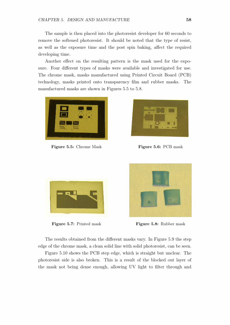
CHAPTER 5. DESIGN AND MANUFACTURE 58
The sample is then placed into the photoresist developer for 60 seconds toremove the softened photoresist. It should be noted that the type of resist,as well as the exposure time and the post spin baking, affect the requireddeveloping time.
Another effect on the resulting pattern is the mask used for the expo-sure. Four different types of masks were available and investigated for use.The chrome mask, masks manufactured using Printed Circuit Board (PCB)technology, masks printed onto transparency film and rubber masks. Themanufactured masks are shown in Figures 5.5 to 5.8.
Figure 5.5: Chrome Mask Figure 5.6: PCB mask
Figure 5.7: Printed mask Figure 5.8: Rubber mask
The results obtained from the different masks vary. In Figure 5.9 the stepedge of the chrome mask, a clean solid line with solid photoresist, can be seen.
Figure 5.10 shows the PCB step edge, which is straight but unclear. Thephotoresist side is also broken. This is a result of the blocked out layer ofthe mask not being dense enough, allowing UV light to filter through and

CHAPTER 5. DESIGN AND MANUFACTURE 59
compromise the photoresist. This type of mask can work, if a denser masklayer can be achieved.
Figure 5.11 shows the result of the mask printed onto transparency film.The step edge is unclear, uneven and the photoresist is compromised. This isa result of the loose packing of the toner onto the film.
Lastly, Figure 5.12 shows the rubber mask step edge. The line is unevenbut clear, also the photoresist is unbroken. The step unevenness is due to hoethe rubber was cut. A more solid cut will yield a finer step edge.
Figure 5.9: Photoresist profile of achrome mask
Figure 5.10: Photoresist profile of a PCBmask
Figure 5.11: Photoresist profile of aprinted mask
Figure 5.12: Photoresist profile of a rub-ber mask
Given the results and the geometries of the masks it is noted that the rubbermask is only usable for larger pattern geometries. While improved forms ofthe PCB and printed masks can be used for smaller geometries, the chromemask is the only one that can be used for micron and sub-micron structures.

CHAPTER 5. DESIGN AND MANUFACTURE 60
The microelectronics laboratory usually acquires outdated photoresist, dueto the cost of fresh photoresist. For the use that it gets employed in the clean-room, the only real difference is that the outdated resist does not provide sucha well defined a under-etch and the time parameters of the sample preparationalso change slightly.

CHAPTER 5. DESIGN AND MANUFACTURE 61
Thermal evaporation
Once a sample is ready for material deposition, one method of doing so is byusing the thermal deposition unit. In Figure 5.13, the laboratory’s RIBERmodel thermal evaporator can be seen.
Figure 5.13: Thermal evaporation unit
The thermal evaporation unit requires a crucible, coil or basket to beclamped between its electrodes for heating, as shown in Figure 5.14. Thecleanroom mostly uses tungsten crucibles for thermal deposition. A materialplaced in the crucible sublimates and deposits on the waiting sample. Be-fore depositing a new material, a crucible must first be prepared. This entailscleaning it with acetone and then annealing it in the thermal evaporator.
The annealing process requires the crucible to be placed into the thermalevaporation unit without material in it. The unit is then sealed, as for a normaldeposition, and then turned up to maximum current. This burns the crucibleclean and expunges any latent gas in the crucible. A crucible being annealedin a dark room can be seen in Figure 5.15.

CHAPTER 5. DESIGN AND MANUFACTURE 62
Figure 5.14: Thermal evaporation unitcrucible
Figure 5.15: Thermal evaporation unitduring annealing process
Once the crucible is annealed, it is loaded with a suitable material and asensor placed in the QCM. The sample also is placed in the thermal evaporator.The glass dome is put in place and the vacuum is allowed to reach 10−6mbar.the current is slowly increased until the required deposition temperature isreached.
The QCM is used to control the deposition rate and thickness of the de-posited material. Having completed this phase, the current is turned down andthe vacuum is vented. This completes the deposition process. Having removedthe sample, it is placed in the photoresist remover to corrode the extraneousmaterial, leaving the required structure behind.
It should be noted that the sensor needs to be calibrated for the firstdeposition and again for every 10% loss of sensor life. For even more accuratedepositions a calibration sample can be placed in the unit, along with everydeposition, for continuous calibration.
Slow heating and cooling of the crucible is important since heating it tooquickly can destroy the crucible. This should be avoided due to material lossand the waste of the 2 hours required for a deposition.
The components of the QCM are shown in Figure 5.16. For the accu-rate operation of the QCM the Z-factor, tooling factor and the density of the
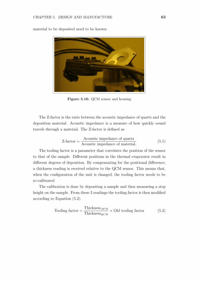
CHAPTER 5. DESIGN AND MANUFACTURE 63
material to be deposited need to be known.
Figure 5.16: QCM sensor and housing
The Z-factor is the ratio between the acoustic impedance of quartz and thedeposition material. Acoustic impedance is a measure of how quickly soundtravels through a material. The Z-factor is defined as
Z-factor =Acoustic impedance of quartz
Acoustic impedance of material.(5.1)
The tooling factor is a parameter that correlates the position of the sensorto that of the sample. Different positions in the thermal evaporator result indifferent degrees of deposition. By compensating for the positional difference,a thickness reading is received relative to the QCM sensor. This means that,when the configuration of the unit is changed, the tooling factor needs to bere-calibrated
The calibration is done by depositing a sample and then measuring a stepheight on the sample. From these 2 readings the tooling factor is then modifiedaccording to Equation (5.2).
Tooling factor =ThicknessAFMThicknessQCM
×Old tooling factor (5.2)

CHAPTER 5. DESIGN AND MANUFACTURE 64
AFM
The Nanosurf Easyscan2 and its peripherals can be seen in Figure 5.17. Theperipherals include a stable table and a motorised stepper. The stable table isused to cancel out the vibrations from the environment, since the AFM probeis highly sensitive.
Figure 5.17: AFM station
The stepper is used to move the sample around before or during a scan toget to the right position for scanning. In Figure 5.18 a closer view of the AFMand stepper is provided.
Figure 5.18: The AFM and motorised sample base

CHAPTER 5. DESIGN AND MANUFACTURE 65
Once a sample has been placed under the AFM, the tip is advanced towardsthe sample and then allowed to make the final approach on its own. This isto prevent the tip from crashing into the surface.
The scan starts automatically. When the scan is completed, the data canbe represented as a line graph, colour map or 3D representation. The tipwithdraws on its own, to prevent vibrations or swivelling to damage it on thesurface.
Structures higher than 1 micron should not be scanned with the AFM, sincethe height differences during the scan can damage the probe. The correct tipfor the scan to be undertaken should be selected, to ensure accurate readingsand mode operation.
When attempting AFM scratching, contact tips should be used. These tipsare shorter and sturdier than the tap mode tips. This makes them less flexibleand better for scraping away material.

CHAPTER 5. DESIGN AND MANUFACTURE 66
5.3 Choosing a Device
In Chapter 3, a brief overview of some of the nanoswitches currently makingprogress and impact on the field of sub-micron switching was given. Now itis necessary to make a choice between these switches for the next step in theresearch objective. To this end a means must be found to choose between theavailable 9 switches:
1. Silver sulfide nanoswitches
2. Phototransistor type nanoswitches using nanoribbons
3. Metal/Organic insulator/Metal type photoswitches
4. Nanofiber switches
5. CNT one side suspended cantilever nanoswitches
6. CNT double suspended cantilever nanoswitches
7. CNT actuated bearing type nanoswitches
8. C70 - CNT nanoswitches
9. Organic motor nanoswitches
To this end a variation on the decision-matrix, or Pugh’s method was used.In this method, important criteria for the final device are defined and givenrelative values. Each of the devices is then rated against these criteria, andthe device with the highest score is then considered the most viable [39]. Theweighting value was taken out of a total of ten, with no two criteria allowedto have the same weighting, in this case 4, 3, 2 and 1.
Four criteria for the nanoswitches were identified, in descending weightingorder:
• A: Manufacturability of the device in the microelectronic laboratory
• B: Applicability to mechanical switching and logic gates
• C: Cost of materials and manufacture
• D: Switching rate of the device
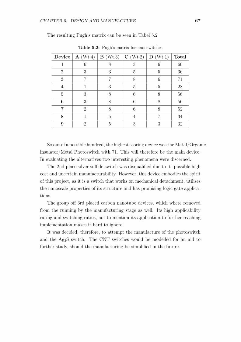
CHAPTER 5. DESIGN AND MANUFACTURE 67
The resulting Pugh’s matrix can be seen in Tabel 5.2
Table 5.2: Pugh’s matrix for nanoswitches
Device A (Wt.4) B (Wt.3) C (Wt.2) D (Wt.1) Total1 6 8 3 6 602 3 3 5 5 363 7 7 8 6 714 1 3 5 5 285 3 8 6 8 566 3 8 6 8 567 2 8 6 8 528 1 5 4 7 349 2 5 3 3 32
So out of a possible hundred, the highest scoring device was the Metal/Organicinsulator/Metal Photoswitch with 71. This will therefore be the main device.In evaluating the alternatives two interesting phenomena were discerned.
The 2nd place silver sulfide switch was disqualified due to its possible highcost and uncertain manufacturability. However, this device embodies the spiritof this project, as it is a switch that works on mechanical detachment, utilisesthe nanoscale properties of its structure and has promising logic gate applica-tions.
The group off 3rd placed carbon nanotube devices, which where removedfrom the running by the manufacturing stage as well. Its high applicabilityrating and switching ratios, not to mention its application to further reachingimplementation makes it hard to ignore.
It was decided, therefore, to attempt the manufacture of the photoswitchand the Ag2S switch. The CNT switches would be modelled for an aid tofurther study, should the manufacturing be simplified in the future.

CHAPTER 5. DESIGN AND MANUFACTURE 68
5.4 Manufacture
Photoswitch
In the original article appertaining to photoswitches of the type metal/organicinsulator/metal by Xinjun Xu et al. [28] a series of devices were manufactured.These devices were created using varying thicknesses of polymethylmethacry-late, polystyrene, gold (Au) and aluminium (Al). The materials were layeredonto a glass substrate with an ITO coating, which would serve as the bot-tom contact and the incidental surface for the UV exposure. The structure ofthe three main devices are represented in Table 5.3, as the organic and metalmaterials that were deposited onto the ITO glass.
Table 5.3: Photoswitch device configurations for manufacture
Device Thickness PMMA Thickness PS Thickness Au Thickness Al1 - 30nm 30nm -2 - 65nm 30nm -3 100nm - - 50nm
To gain a quick feel for the structure involved, two devices were attempted.The first was ITO glass (9-15 sq/Ω), PMMA photoresist, hard baked, and thenlayered with gold using the DC sputtering unit. The second was ITO, the or-ganic semiconductor copper phthalocyanine (CuPc) and gold sputtering. Theexperiments yielded several results for contemplation. These initial devices areshown in Figure 5.19.
Figure 5.19: Test run photoswitches

CHAPTER 5. DESIGN AND MANUFACTURE 69
The PMMA photoresist did not work well as an organic insulator, due tothe soft nature of the layer, even after baking. At the time, there was also noreliable way to verify the layer thicknesses of the spun on PMMA photoresistor the sputtered gold.
The metal electrodes needed to be deposited at a rate of 0.5Å /s in athermal evaporation unit at a vacuum of at least 1.5×10⁻⁴. This being knownand with the experience of the first attempt, it was noted that the QuartzCrystal Microbalance (QCM) sensor could be used to control the depositionrate and control the layer thickness.
The QCM sensor works by measuring the change in frequency of the quartzcrystal resonator, which is dependant on the deposition of material on itsacoustic interface. This allows for the accurate determination of depositionrates and film thicknesses, given the density, acoustic impedance and a cali-bration run to determine the tooling factor of the sensor.
Further research into the deposition of PMMA and PS material eventuallyled to a reference on isolating individual zinc oxide nanotubes from one an-other for an electroluminescence application [40]. It states that PS depositionstypically involve solutions of PS in toluene.
In an extract from the doctoral work of Alexis Ryan Abramson [41], itwas found that polystyrene could be used to add mechanical strength to aloose nanocomposite. The polystyrene was disolved in a 1:10 mass ratio of PSto toluene. The resulting organic layer had good mechanical strength and asoftening temperature of 200C. It was also stated that its chemical resistancewas questionable.
The final result for the manufacture of the organic polymer for devicedelivery used 2mg/ml of polystyrene in a mixture of toluene and xylene ina 1:1 ratio at room temperature [42]. The solution is then sonicated for 10minutes to ensure thorough particle distribution.
Care should be taken to prevent water from being included during themixing process, since it causes the polystyrene to particulate. This is easilyspotted, since the solution will turn a milky white if this occurs.
The nanophotoswitch article used polystyrene (MW 65000) for its organiclayer [28]. A polystyrene development kit was therefore purchased from SigmaAldrich. The kit contained 250 mg of polystyrene in a series of molecularweights ranging from MW 5000 - 58000. This would allow testing of a variety
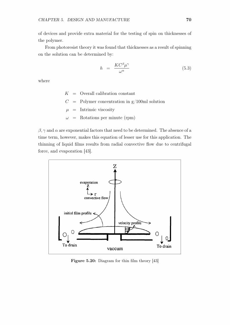
CHAPTER 5. DESIGN AND MANUFACTURE 70
of devices and provide extra material for the testing of spin on thicknesses ofthe polymer.
From photoresist theory it was found that thicknesses as a result of spinningon the solution can be determined by:
h =KCβµγ
ωα(5.3)
where
K = Overall calibration constant
C = Polymer concentration in g/100ml solution
µ = Intrinsic viscosity
ω = Rotations per minute (rpm)
β, γ and α are exponential factors that need to be determined. The absence of atime term, however, makes this equation of lesser use for this application. Thethinning of liquid films results from radial convective flow due to centrifugalforce, and evaporation [43].
Figure 5.20: Diagram for thin film theory [43]

CHAPTER 5. DESIGN AND MANUFACTURE 71
Considering an isothermic, incompressible and homogeneous Newtonianfluid, the spinning forces represented in Figure 5.20 can be represented byEquation 5.4. For fast spinning, faster than 1000rpm, this equation can bereduced to the form of Equation (5.5).
h =
√h2
043ρω2µh2
0t+ 1(5.4)
h =
√3
2ω√ρµt
(5.5)
in these equations h is the thickness of the film, h0 is a characteristic scalingfactor, ω is the rotational speed of the disc in rpm, ρ is the density of the fluid,µ is the viscosity of the fluid and t is the spinning time.
It should be noted that initial film thickness has no effect on the final filmthickness [43], unless the amount of fluid was insufficient to coat the surface.
Molar mass of polystyrene is dependant on the clustering of the moleculesand can be controlled by the manufacturing process and quality control. Thespecific molecular weight of the material used should always be stated withthe material.
Health considerations, when using toluene and xylene, depend on exposureand duration, as well as genetic susceptibility and age. Toluene can causetiredness, confusion, weakness, drunken-type actions, memory loss, nausea,and loss of appetite under low exposure. High levels of exposure can precipitatedizziness, sleepiness, or unconsciousness. Death is also possible, due to howtoluene interferes with the way breathing and the way the heart beats. It doesnot, however, cause cancer [44]. With short term exposure xylene can causeirritation of the skin, eyes, nose, and throat, difficulty in breathing, impairedfunction of the lungs, delayed response to a visual stimulus, impaired memory,stomach discomfort, and possible changes in the liver and kidneys. The effectsof long term exposure to xylene is similar to that of toluene, but the possibilityof it causing cancer has not as yet been properly tested [45]. Polystyrene hasbeen classified as a possible carcinogenic material.
Therefore, while working with the compounds for the production of theorganic insulation layer, gloves, mask and eye protection will be worn, in ac-
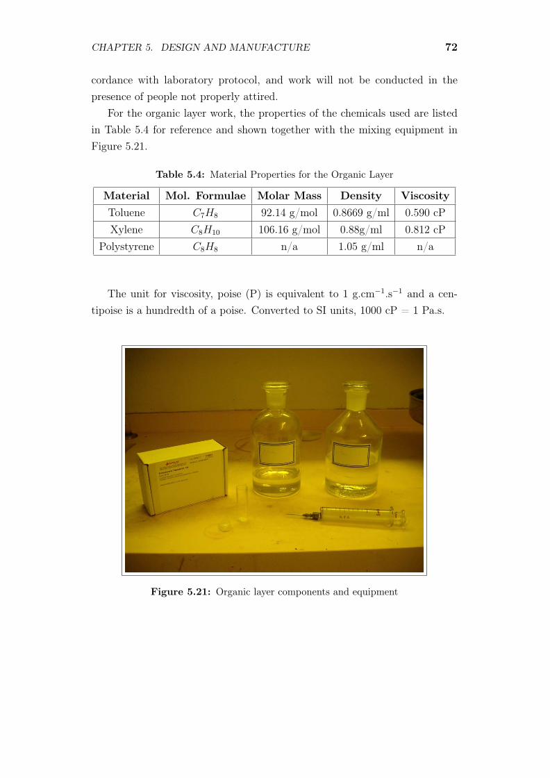
CHAPTER 5. DESIGN AND MANUFACTURE 72
cordance with laboratory protocol, and work will not be conducted in thepresence of people not properly attired.
For the organic layer work, the properties of the chemicals used are listedin Table 5.4 for reference and shown together with the mixing equipment inFigure 5.21.
Table 5.4: Material Properties for the Organic Layer
Material Mol. Formulae Molar Mass Density ViscosityToluene C7H8 92.14 g/mol 0.8669 g/ml 0.590 cPXylene C8H10 106.16 g/mol 0.88g/ml 0.812 cP
Polystyrene C8H8 n/a 1.05 g/ml n/a
The unit for viscosity, poise (P) is equivalent to 1 g.cm−1.s−1 and a cen-tipoise is a hundredth of a poise. Converted to SI units, 1000 cP = 1 Pa.s.
Figure 5.21: Organic layer components and equipment
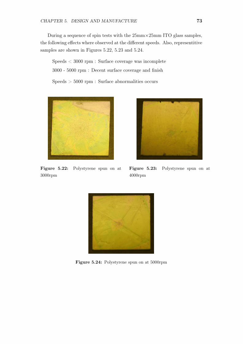
CHAPTER 5. DESIGN AND MANUFACTURE 73
During a sequence of spin tests with the 25mm×25mm ITO glass samples,the following effects where observed at the different speeds. Also, representitivesamples are shown in Figures 5.22, 5.23 and 5.24.
Speeds < 3000 rpm : Surface coverage was incomplete
3000 - 5000 rpm : Decent surface coverage and finish
Speeds > 5000 rpm : Surface abnormalities occurs
Figure 5.22: Polystyrene spun on at3000rpm
Figure 5.23: Polystyrene spun on at4000rpm
Figure 5.24: Polystyrene spun on at 5000rpm
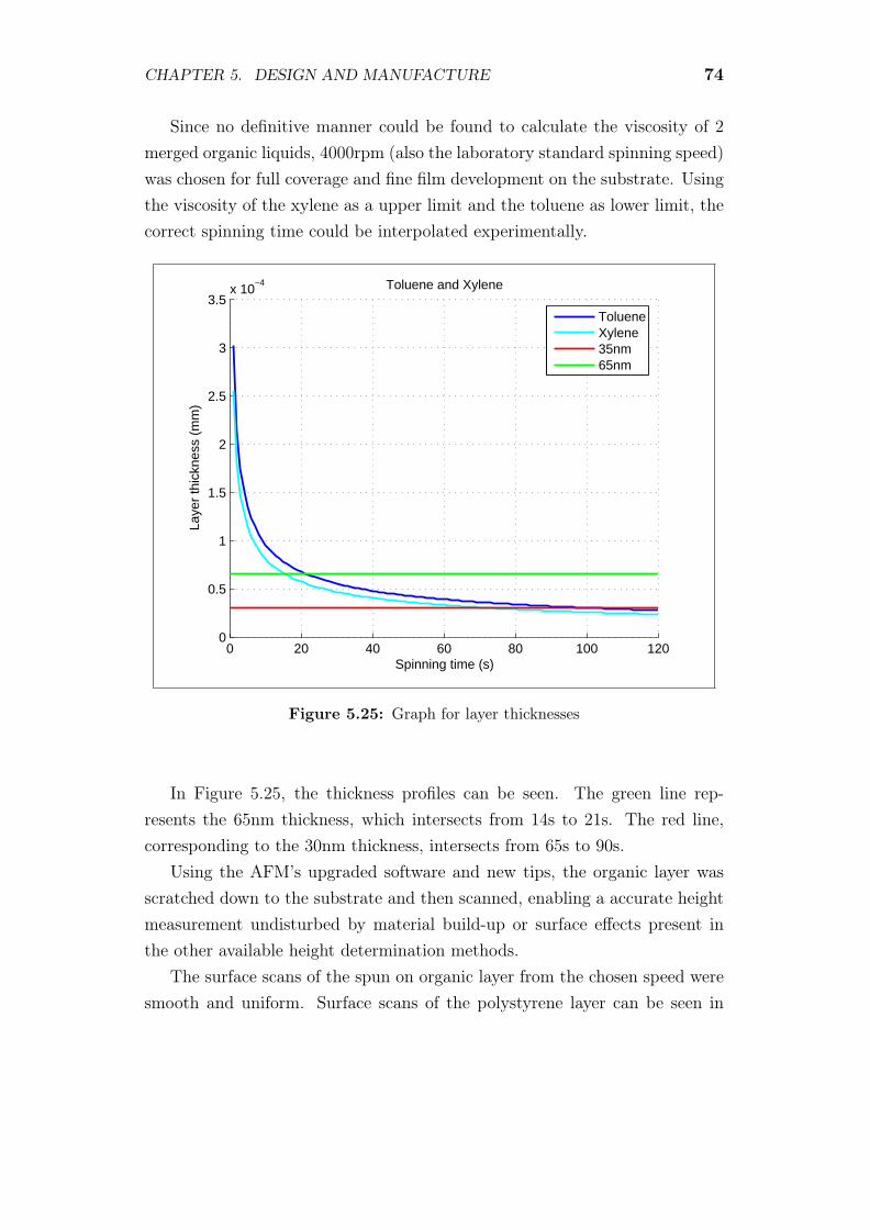
CHAPTER 5. DESIGN AND MANUFACTURE 74
Since no definitive manner could be found to calculate the viscosity of 2merged organic liquids, 4000rpm (also the laboratory standard spinning speed)was chosen for full coverage and fine film development on the substrate. Usingthe viscosity of the xylene as a upper limit and the toluene as lower limit, thecorrect spinning time could be interpolated experimentally.
0 20 40 60 80 100 1200
0.5
1
1.5
2
2.5
3
3.5x 10
−4
Spinning time (s)
Laye
r th
ickn
ess
(mm
)
Toluene and Xylene
TolueneXylene35nm65nm
Figure 5.25: Graph for layer thicknesses
In Figure 5.25, the thickness profiles can be seen. The green line rep-resents the 65nm thickness, which intersects from 14s to 21s. The red line,corresponding to the 30nm thickness, intersects from 65s to 90s.
Using the AFM’s upgraded software and new tips, the organic layer wasscratched down to the substrate and then scanned, enabling a accurate heightmeasurement undisturbed by material build-up or surface effects present inthe other available height determination methods.
The surface scans of the spun on organic layer from the chosen speed weresmooth and uniform. Surface scans of the polystyrene layer can be seen in
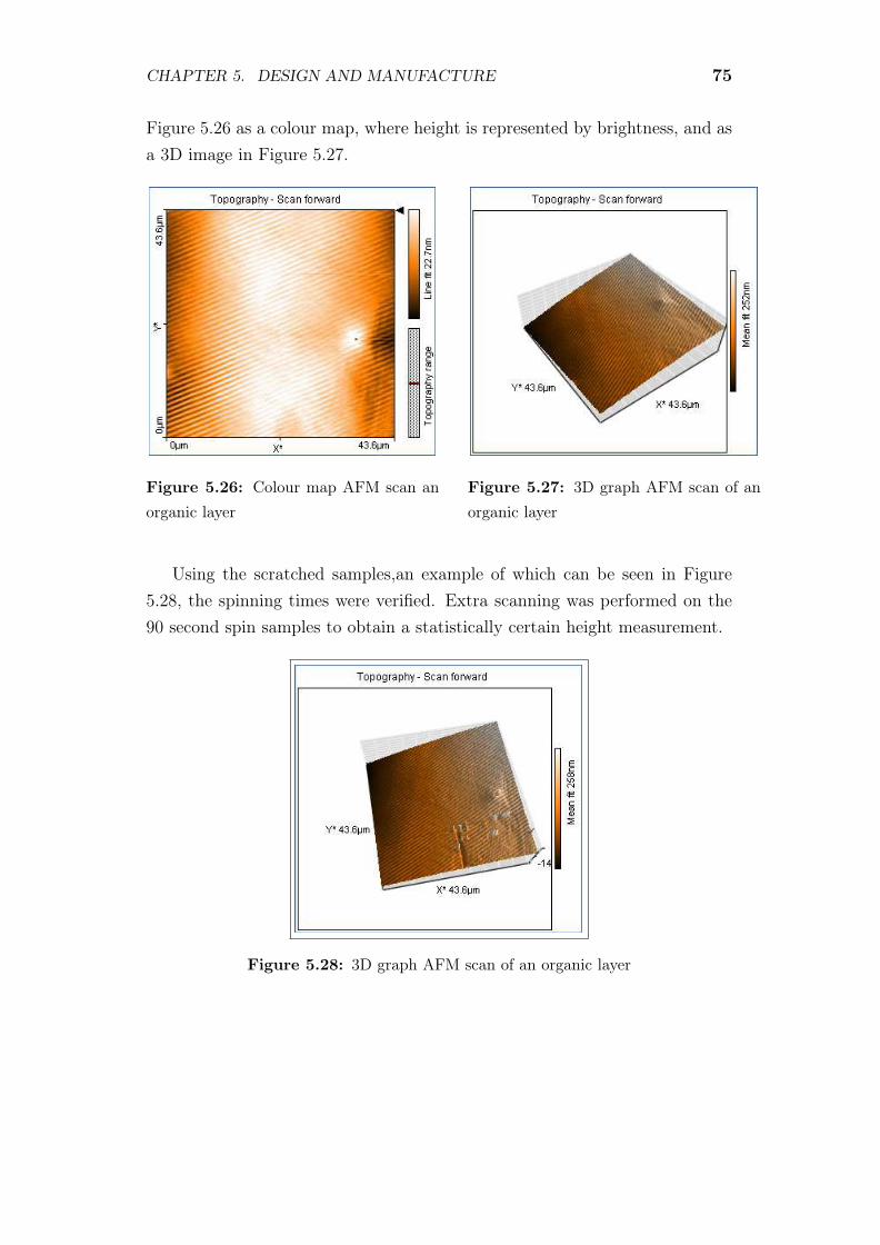
CHAPTER 5. DESIGN AND MANUFACTURE 75
Figure 5.26 as a colour map, where height is represented by brightness, and asa 3D image in Figure 5.27.
Figure 5.26: Colour map AFM scan anorganic layer
Figure 5.27: 3D graph AFM scan of anorganic layer
Using the scratched samples,an example of which can be seen in Figure5.28, the spinning times were verified. Extra scanning was performed on the90 second spin samples to obtain a statistically certain height measurement.
Figure 5.28: 3D graph AFM scan of an organic layer

CHAPTER 5. DESIGN AND MANUFACTURE 76
This was required since the cross cuts of the scratches, as in Figure 5.29were not consistent. From a sample group of thickness data shown in Table5.5, finite statistics can be used to obtain the mean value and the standarddeviation of the measurements.
Figure 5.29: Cross section of the AFM scratch
Table 5.5: Organic layer thickness readings
Sample i Thickness x (nm)1 25.942 24.913 22.244 31.055 51.526 10.087 25.098 22.089 31.6110 37.02
Having first removed terms 5 and 6 due to there being sample anoma-lies, the working of the data could commence. Using a Gaussian statisticaldistribution [24], from Equation (5.6), given that there are N samples with

CHAPTER 5. DESIGN AND MANUFACTURE 77
(xi) being the i -th measurement, the mean (x of the system is 27.49nm. Thisyielded the sample deviance through the measurements as 5.29nm, from Equa-tion 5.9, meaning that 68% of the thicknesses will lie in the range of 22.20nmto 32.78nm.
x =1
N
∑xi (5.6)
S2x =
1
N − 1
∑(xi − x)2 (5.7)
Sx =√S2x (5.8)
=
√1
N − 1
∑(xi − x)2
(5.9)
The reason for this can be seen in Figure 5.30. Inside the scratched trenchthere are height anomalies, probably due to loosened photoresist and ITOpeaks. From this scan, the flattening depth of the scratch can be seen to be26nm, very close to the calculated mean and well within the deviance range.The difference can be explained by finite statistics using only a limited numberof data points. Should an infinite number of data points be used, the calculatedmean would be theoretically identical to the lengthwise cross section.
Figure 5.30: Cross section along the AFM scratch

CHAPTER 5. DESIGN AND MANUFACTURE 78
The height values deviated from the values for toluene and xylene, as ex-pected, due to the mixed fluid and suspended polystyrene. This data wasplugged back into Equation 5.5 to obtain the characteristic profile for themixture.
The first round of adapted photoswitches that where attempted with 30nmPS and 30nm aluminium, seen in Figure 5.31, did not function satisfactorily.There was continuity through the device.
Figure 5.31: First complete photoswitch
Looking at the surface roughness of the ITO glass, seen in Figure 5.32,which in some areas show varying peaks of up to 60nm. In Figure 5.33 thecross cut of the ITO surface can clearly be seen to have a high level of variance.
A device using the parameters of 120nm PS and 50nm aluminium was tobe created. This would place the top electrode 100nm, plus the additionalmean ITO height difference of 20nm, above the ITO contact.
Figure 5.32: 3D graph AFM scan of theITO glass
Figure 5.33: Cross section of the ITOglass surface
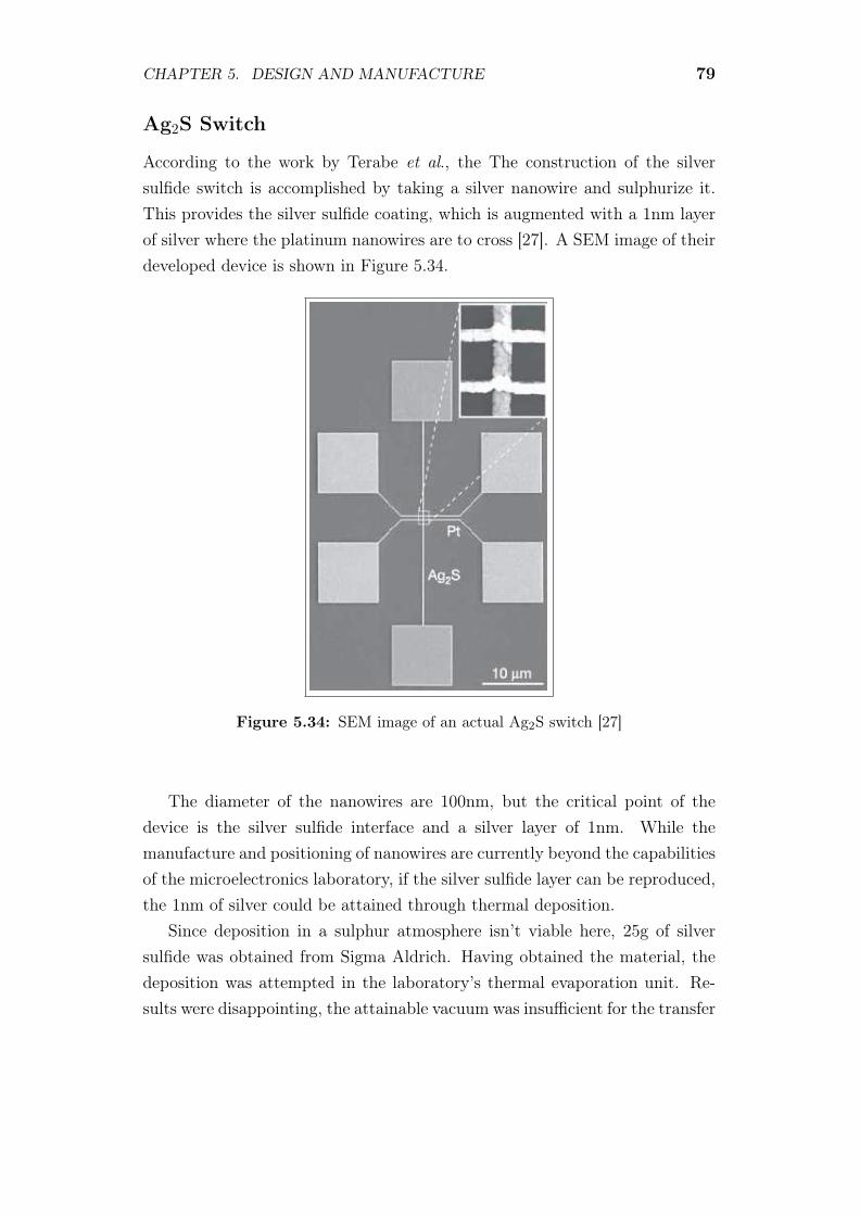
CHAPTER 5. DESIGN AND MANUFACTURE 79
Ag2S Switch
According to the work by Terabe et al., the The construction of the silversulfide switch is accomplished by taking a silver nanowire and sulphurize it.This provides the silver sulfide coating, which is augmented with a 1nm layerof silver where the platinum nanowires are to cross [27]. A SEM image of theirdeveloped device is shown in Figure 5.34.
Figure 5.34: SEM image of an actual Ag2S switch [27]
The diameter of the nanowires are 100nm, but the critical point of thedevice is the silver sulfide interface and a silver layer of 1nm. While themanufacture and positioning of nanowires are currently beyond the capabilitiesof the microelectronics laboratory, if the silver sulfide layer can be reproduced,the 1nm of silver could be attained through thermal deposition.
Since deposition in a sulphur atmosphere isn’t viable here, 25g of silversulfide was obtained from Sigma Aldrich. Having obtained the material, thedeposition was attempted in the laboratory’s thermal evaporation unit. Re-sults were disappointing, the attainable vacuum was insufficient for the transfer

CHAPTER 5. DESIGN AND MANUFACTURE 80
of the silver sulfide, instead the heat split the compound producing sulphurgas and silver deposition.
Since the silver sulfide couldn’t be added onto the silver, ways were soughtto infuse the sulphur without using a sulphurous atmosphere. It was foundthat old Russian jewellers used a compound called niello to produce blackenedsilverware like that seen in Figure 5.35. This compound is a mixture of silver,lead, copper, sulphur and ammonium chloride. The specific formula is jew-eller dependant and is handed down within a family of jewellers, although astandardised commercial variant is available.
Figure 5.35: Niello Silverware [46]
Jewellers’ preferred method for the sulphurization of silver, however, isusing liver of sulphur. This mixture is prepared as a brown clump, as in Figure5.36, by combining sulphur and potassium carbonate. A diluted solution ofthis compound can be used to sulphurize silver. However, the fumes given offduring this process is toxic.

CHAPTER 5. DESIGN AND MANUFACTURE 81
Figure 5.36: Liver of Sulphur
A less toxic method, along the same lines, is to use lime sulphur. It isconsiderably cheaper than liver of sulphur and available at most agriculturalsuppliers as a pesticide. The chemical name is calcium polysulfide, and it iscreated by mixing calcium hydroxide and sulphur [47].
A test was done to determine if this method would yield satisfatory results.To determine the nature of the result, a 69% solution of nitric acid (HNO3)would be used, since it dissolves silver but only attacks silver sulfide. First thediscerning test was attempted with plain silver and the acquired silver sulfide.The silver dissolved and the Silver sulfide remained, as seen in Figure 5.37.
Figure 5.37: The impregnated silver tested in nitric acid
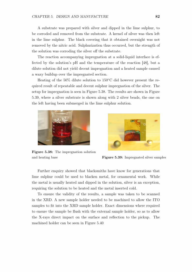
CHAPTER 5. DESIGN AND MANUFACTURE 82
A substrate was prepared with silver and dipped in the lime sulphur, tobe corroded and removed from the substrate. A kernel of silver was then leftin the lime sulphur. The black covering that it obtained overnight was notremoved by the nitric acid. Sulphurization thus occurred, but the strength ofthe solution was corroding the silver off the substrate.
The reaction accompanying impregnation at a solid-liquid interface is ef-fected by the solution’s pH and the temperature of the reaction [48], but adilute solution did not yield decent impregnation and a heated sample causeda waxy buildup over the impregnated section.
Heating of the 50% dilute solution to 150C did however present the re-quired result of repeatable and decent sulphur impregnation of the silver. Thesetup for impregnation is seen in Figure 5.38. The results are shown in Figure5.39, where a silver substrate is shown along with 2 silver beads, the one onthe left having been submerged in the lime sulphur solution.
Figure 5.38: The impregnation solutionand heating base Figure 5.39: Impregnated silver samples
Further enquiry showed that blacksmiths have know for generations thatlime sulphur could be used to blacken metal, for ornamental work. Whilethe metal is usually heated and dipped in the solution, silver is an exception,requiring the solution to be heated and the metal inserted cold.
To ensure the validity of the results, a sample was taken to be scannedin the XRD. A new sample holder needed to be machined to allow the ITOsamples to fit into the XRD sample holder. Exact dimensions where requiredto ensure the sample be flush with the external sample holder, so as to allowthe X-rays direct impact on the surface and reflection to the pickup. Themachined holder can be seen in Figure 5.40

CHAPTER 5. DESIGN AND MANUFACTURE 83
Figure 5.40: XRD sample holder
In Figure 5.41 the scanned spectrum can be seen. The relevant peaks forsilver sulfide were identified and verified. A explanation of the verification ofthe silver sulfide and other relavant materials can be found in Addendum C.
Figure 5.41: XRD results for silver sulfide development
The silver sulfide can thus be reproduced and the small 1nm thick interfacecan be reproduced using the organic insulator from the photoswitch, making

CHAPTER 5. DESIGN AND MANUFACTURE 84
an AFM scratch and deposition of the controlled silver with the thermal evap-oration unit.
Figure 5.42: Test run device for the silver sulfide switch
Having the critical components in order, a test switch seen in Figure 5.42was to be built, non functional, just to test the off-state characteristics of theswitch. Since the platinum is very expensive, the system was to be checked tomake sure it would in fact deposit the material.
Table 5.6: Material Data for Thermal Deposition (in Celsius)
Material Melting Point Sublimation at 10−5mbarSilver 962C 958C
Platinum 1772C 1492CBoron 2300C 1548C
Palladium 1554C 992CAluminium 660C 821C
Some thermal evaporation data has been provided in Table 5.6 [49], withthe full list available in Addendum B.
The rated temperature for platinum deposition seemed somewhat high forthe available unit, so a sample was made with some available boron, havinga similar deposition temperature. The thermal evaporation unit was barely

CHAPTER 5. DESIGN AND MANUFACTURE 85
able to reach the required temperature and vacuum, at the same time glowinglike a light bulb. After the annual service of the unit, could not reach therequired temperature again, due to a reduction in resistance of the cruciblearm. Platinum could thus not be deposited.
To find a metal with similar chemical properties as platinum, materials ingroup 7 of the periodic table were looked at. Palladium, being in the samecolumn and only one row removed seemed like a promising candidate. At992C it is also well within the capability of the thermal evaporation unit.Purchase of the material became unnecessary when iThemba Labs donated 2gof Palladium to the project.
An XRD scan was made of a palladium deposition to ensure purity, sinceduring thermal evaporation it releases an inordinate amount of oxygen. Duringthe first calibration runs, the material even started to spit and catch alight dueto the poor vacuum caused by its de-gasing. By allowing the vacuum to reacha level of 5× 10⁻⁶mbar the de-gasing problem is overcome, but the reachabletemperatures only allow for thermionic deposition.
Once all the materials had been calibrated and synthesis ensured, a devicewas made. The parameters for the silver sulfide switch, in order, were tobe 100nm silver, a 20nm insulation layer, the 1nm silver layer and 100nmpalladium layer.
A primary device was made simply layering the materials, without theinsulator. This was to develop a feel for the process and have a reference tothe device on state. the device showed an on current of 55mA for 600mVactivation voltage, hence an internal resistance of 10.91Ω. Having seen thatthe completed test device had through conduction, this was followed by a planfor the full device.
The silver base electrode is deposited onto the Silicon substrate and theorganic insulator spun on. The sample then has a few trenches scratched intothe insulator and placed into the lime sulphur for impregnation. Then to thethermal evaporation unit for deposition. The 1nm silver and 100nm palladiumis done directly after one another to prevent contamination in the atmosphere.This double deposition without breaking vacuum is possible due to the twocrucible modification of the thermal evaporator.

CHAPTER 5. DESIGN AND MANUFACTURE 86
5.5 Results
In the final manufacturing procedures, all attention was given to ensure asclean a working environment as was possible. All surfaces and equipment werewashed of with acetone or ethanol, depending on their requirements. Sampleswere treated in an acetone sonic bath and then annealed. No cross contami-nation of materials was allowed and all stages of production were treated withnitrogen to prevent oxidation and the occurrence of foreign particles.
Photoswitch
The last iteration of photoswitch production, yielded 3 devices of a testablecalibre. A testing area was prepared around the UV exposer and 2 multimeterswere acquired along with a 8V/40V power supply. The complete setup can beseen in Figure 5.43, along with a closer view of the exposure zone in Figure5.44.
Figure 5.43: Photoswitch testing area Figure 5.44: UV exposure zone
The first multimeter was used to measure the current through the devicewhile the second was used to verify the supply voltage. All masks and coverswere removed from the UV exposer.
The initial sample was placed on the test rig with an ionic water solution toensure electrical contact. Unfortunately, due to the reactive nature of copper,water surface tension and the very thin layer of aluminium, the device’s surfacesuffered cavitation. An image of the device, post cavitation, is given in Figure
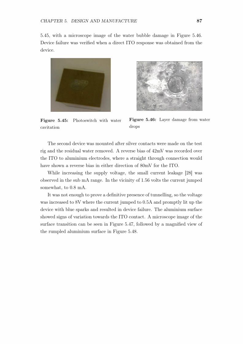
CHAPTER 5. DESIGN AND MANUFACTURE 87
5.45, with a microscope image of the water bubble damage in Figure 5.46.Device failure was verified when a direct ITO response was obtained from thedevice.
Figure 5.45: Photoswitch with watercavitation
Figure 5.46: Layer damage from waterdrops
The second device was mounted after silver contacts were made on the testrig and the residual water removed. A reverse bias of 42mV was recorded overthe ITO to aluminium electrodes, where a straight through connection wouldhave shown a reverse bias in either direction of 80mV for the ITO.
While increasing the supply voltage, the small current leakage [28] wasobserved in the sub mA range. In the vicinity of 1.56 volts the current jumpedsomewhat, to 0.8 mA.
It was not enough to prove a definitive presence of tunnelling, so the voltagewas increased to 8V where the current jumped to 0.5A and promptly lit up thedevice with blue sparks and resulted in device failure. The aluminium surfaceshowed signs of variation towards the ITO contact. A microscope image of thesurface transition can be seen in Figure 5.47, followed by a magnified view ofthe rumpled aluminium surface in Figure 5.48.

CHAPTER 5. DESIGN AND MANUFACTURE 88
Figure 5.47: Aluminium distortion tran-sition
Figure 5.48: Magnified view of alu-minium deformation
Following the current breakthrough, a test was run on a standard ITO glass.When the power reached 4 Watts the ITO cracked due to electrical stresses.The height of the cracked sections exceeds 1 micron, making it impossible toscan with the AFM. In Figure 5.49 the device and ITO glass that underwentarcing can be seen, along with a microscope image of the ITO cracking inFigure 5.50.
Figure 5.49: Arc damaged samples Figure 5.50: Magnified ITO fractures
The final device was then mounted on the test rig with only touch contacts.Diode testing showed a reverse bias of 35mV. The current was then increasedto the initial current jump to activate the metal tunnelling. From 2.0V up to2.5V a gradually speeding increase of current could be seen as, theoretically,tendrils penetrated the organic layer. Reducing the input voltage to 0.5V, thesample was exposed to UV light after which the 200mA current vanished.
A deviation from the relevant literature at this point was that, to rearmthe device, the voltage needed to be ramped up to 1V to reinitialise the metal

CHAPTER 5. DESIGN AND MANUFACTURE 89
filaments for current flow, after which the UV again reduced the current tozero.
After 7 runs of switching, however, the device also failed due to condensa-tion from the UV exposer.
The voltage span of 0.5V to 1V for metal filament growth and switchingfollows the expected behaviour. Also, the current achieved was congruent withsimilar devices in the literature. Unfortunately the actual off-state currentcould not be measured since it should be in the pico ampere range, but adefinite off-state was evident.
Although tenuous, the fabricated switch configuration thus was operationaland showed repeatable switching.

CHAPTER 5. DESIGN AND MANUFACTURE 90
Silver Sulfide Switch
Two devices were produced using the techniques developed during the previoussection. Additionally, a calibration sample was included with the productionsample at every thermal evaporation step to ensure accurate layer thicknesses,particularly during the 1nm silver deposition.
For the palladium deposition, a powder crucible was used instead of theslug crucible used previously. The powder crucible has a higher resistance,hence a higher temperature can be achieved, even melting the palladium.
To test the silver sulfide switches they will be placed on a test rig witha 600mV activation voltage applied, positive to the palladium. If the switchturns off, without it being due to device failure, the reverse voltage shouldreactivate the switch.
Neither switch functioned. While both where conductive and showed a0.06mA current through the device and the bias resistor, no switching wasevident. After the application of a increased activation pre-biasing, for ap-proximately an hour, the devices did show a 10% drop in their current.
Possible reasons for the device failure, from the available data, are materialor interface problems. The material problems may explain why there is noswitching and could be as a result of the palladium or the silver sulfide.
Issues arising from the palladium are that it is a substitute for platinum,and while having the same valence electrons and characteristics, may not shareall of its properties. While sulphur penetration was verified on the switch sam-ples, the penetration depth and molecular configuration from the impregnationmethod used may be non-conducive to this type of switching.
From the slightly reduced current flow after extended biasing, however,it would seem that some electrolytic processes took place. This moves theproblem towards the material interfaces. While the active silver layer is 1nmthick, the length and width of the contact trenches may be to large. Wherethe existing device had contact areas of 100nm×100nm, the trenches made onthe AFM were 9µm×2µm. This equates to an area variation in the order of103, which affects the volume of material to be absorbed.
Another possibility is impurities within the trenches, either from dust orresidual photoresist from the scratching process. This may be overcome bymilling, but the effects on the organic layer must then be tested as well, inorder to confirm no adverse effects on the insulation.

CHAPTER 5. DESIGN AND MANUFACTURE 91
5.6 To Summarise
In this chapter the origins of the cleanroom were related, as well as giving alist of the facilities available there and explaining the use of the more prevalentequipment.
The method used to choose the switches for manufacture was discussed andshown along with the reasoning behind the portions of work to be undertaken.
Following this preamble, the iterative design and manufacture processesfor the photoswitch and silver sulfide switch was shown. This covered theinitial research, the test switches and solving of the resulting manufacturingobstacles.
The final devices where then characterised and manufactured, the testing ofthese devices was recorded comprehensively to show the problems encounteredin the verification process.
Of the two switches, the photoswitch was found to be a complete success,while the silver sulfide switch only showed signs of possible silver absorption.Some suggestions were given as to possible problems in the device, as well asways that they may be overcome.

Chapter 6
Simulation
The side-clamped nanoelectromechanical device configuration, seen in Figure6.1, has become prevalent in the field of nanotechnology, being used for diseasedetectors, cancer treatment, catalyst improvement and beyond.
Figure 6.1: Schematic of a cantilever switch [50]
Since it is such a far reaching design, this switch type cannot be ignored.While not being able to produce switches of this type, their simulation isequally important, in order to predict their responses, and most importantly,predicting device failure.
Simulation code will therefore be written to emulate the bending and shift-ing in CNT cantilever switches in order to predict failure from the devicegeometry.
92

CHAPTER 6. SIMULATION 93
6.1 CNT Simulation Theory
The analysis of a NEMS structure involves the mechanical analysis of thestructure, as well as the electrostatic analysis. Usually these type of mechanicalstructures would be analysed using molecular dynamics (MD) models. Due tothe relatively large size of the CNT cantilever switch and the large number ofatoms involved, however, it will be too time and computation intensive.
Elastostatic models from the continuum mechanics theory have been widelyused for the analysis of microstructures, and with a few modifications forquantum effects and material adaptation, are viable for NEMS analysis [51].
In standard elastostatic theory, the relation between a material’s stress(σ) and strain (ε) is given by Equation (6.1) [52]. The relating constant Eis Young’s modulus, but due to small scale effects, like reduced material im-perfections and close range adhesion, this relationship changes in the nanoregime. Two ways to compensate for this is by including the small scale pa-rameter correction e0a [53] or by modifying the material parameters to reflectthese changes.
σ(x) = Eε(x) (6.1)
σ(x)− (e0a)2d2σ
dx2= Eε(x) (6.2)
(6.3)
Both the material parameters and e0a are obtained from experiments andMD simulations. The new form of the stress-strain equation is given by Equa-tion 6.2.
The equilibrium requirements of the static states are given by Equations(6.4) and (6.5), where q is force, Q is the shear force in the beam and M is thebending moment. From this the relationship between force and moment canbe derived, as seen in Equation (6.6).

CHAPTER 6. SIMULATION 94
−q(x) =dQ
dx(6.4)
Q =dM
dx(6.5)
q =d2M
dx2(6.6)
The deflection (y) of the beam can be related to the strain by means of arelation constant in the form of Equation (6.7).
ε = −z d2y
dx2(6.7)
Now, by substitution of Equation (6.7) into Equation (6.2), the non-localconstitutive Equation (6.8) [53] is obtained. This, along with the equilibriumequations, can be used to derive the governing equation of the nanobeam,given in Equation (6.9).
M(x)− (e0a)2d2M
dx2= −EI d
2y
dx2(6.8)
d4y
dx4=
q
EI− (e0a)2
EI
d2q
dx2(6.9)
Here I is the second moment of area, which, together with Young’s modu-lus, form the rigidity of the beam. Now, using the beam property that shearstress is the derivative of the beam moment, which is the second derivative ofthe beam deflection [52], the bending and shear force equations can be derived.
M(x) = −EI d2y
dx2− (e0a)2q(x) (6.10)
Q(x) = −EI d3y
dx3− (e0a)2d2q
dx(6.11)
This covers the mechanical aspects of the system, which leaves the elec-trostatic portion. This part of the analysis actually contributes the force, as

CHAPTER 6. SIMULATION 95
can be seen in Equation (6.12). Fe is the electrostatic force and Fn is a forcederived from the small scale parameter, dependant on the size of the device.
q = Fe + Fn (6.12)
Fe =ε0wV
2
2(g − y)2(1 + 0.65
g − yw
) (6.13)
Fwn =
Aw
6π(g − y)3(6.14)
F cn =
π2hcw
240(g − y)4(6.15)
Here, ε0 is the permittivity of a vacuum, A is the Hamaker constant, w isthe beam width, V is the applied voltage, g is the electrode to beam gap andc is the speed of light.
The Fn variances Fwn and F c
n are the Van der Waal’s forces and Casamirforces per unit length of the beam respectively. When the gap between thebeam and the fixed electrode is smaller than 20nm, Fw
n is used, while for gapslarger than 20nm, F c
n is used [50].In MEMS and NEMS cantilever devices, the critical phenomenon of pull-in
must be observed. This refers to the voltage at which the nanobeam will sep-arate and end device functionality. Additionally, for NEMS devices, the effectof intermolecular forces may cause failure even when no voltage is applied,depending solely on device geometry [50].
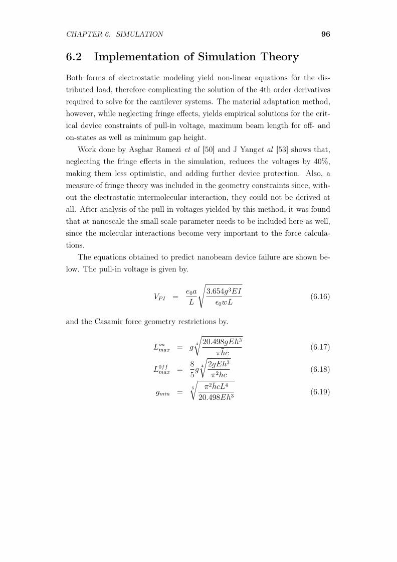
CHAPTER 6. SIMULATION 96
6.2 Implementation of Simulation Theory
Both forms of electrostatic modeling yield non-linear equations for the dis-tributed load, therefore complicating the solution of the 4th order derivativesrequired to solve for the cantilever systems. The material adaptation method,however, while neglecting fringe effects, yields empirical solutions for the crit-ical device constraints of pull-in voltage, maximum beam length for off- andon-states as well as minimum gap height.
Work done by Asghar Ramezi et al [50] and J Yanget al [53] shows that,neglecting the fringe effects in the simulation, reduces the voltages by 40%,making them less optimistic, and adding further device protection. Also, ameasure of fringe theory was included in the geometry constraints since, with-out the electrostatic intermolecular interaction, they could not be derived atall. After analysis of the pull-in voltages yielded by this method, it was foundthat at nanoscale the small scale parameter needs to be included here as well,since the molecular interactions become very important to the force calcula-tions.
The equations obtained to predict nanobeam device failure are shown be-low. The pull-in voltage is given by.
VPI =e0a
L
√3.654g3EI
ε0wL(6.16)
and the Casamir force geometry restrictions by.
Lonmax = g4
√20.498gEh3
πhc(6.17)
L0ffmax =
8
5g
4
√2gEh3
π2hc(6.18)
gmin =5
√π2hcL4
20.498Eh3(6.19)

CHAPTER 6. SIMULATION 97
Lastly, Van der Waal’s force geometry restrictions are given by.
Lonmax =4
√0.657πEh3
A(6.20)
Loffmax =1
2g
4
√27πEh3
4A(6.21)
gmin = L4
√A
0.657πEh3(6.22)
In Figure 6.2, the pull-in voltage VPI can be seen for a CNT nanoswitch oflength 180nm, gap height of 20nm and consisting of a SWNT. The simulationwas modelled over a series of nanotube widths from 10nm to 90nm. The wallthicknesses were varied to reflect the corresponding nanotube diameters.
1 2 3 4 5 6 7 8 90
5
10
15
20
25
30
35Pull−in voltages
Nanotube width (in 10nm increments)
Vol
tage
Pull−in Voltage
Figure 6.2: Graph of the pull-in voltages as a function of geometry
As can be expected, the voltage required to bend the nanotube increasesas the diameter and increasing wall diameter increase its stiffness.

CHAPTER 6. SIMULATION 98
In Figure 6.3, the maximum CNT length, Lmax, is shown for when there isan applied voltage, and when there is none.
1 2 3 4 5 6 7 8 90.2
0.4
0.6
0.8
1
1.2
1.4
1.6
1.8
2x 10
−5 Lengths for failure
Nanotube width (in 10nm increments)
Nan
otub
e le
ngth
(in
m)
Cassimir: Max Length with Voltage
Cassimir: Max Length, no Voltage
Van der Waals: Max Length with Voltage
Van der Waals: Max Length, no Voltage
Figure 6.3: Graph of the nanotube lengths as a function of nanotube diameter
The differing values caused by the Casamir and Van der Waal’s forcesare also shown. Once again, the result reflects the increased strength of thethickening nanotubes. Longer nanotubes can thus be used without fear ofcollapse.
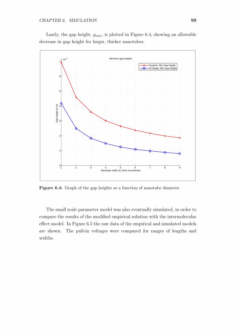
CHAPTER 6. SIMULATION 99
Lastly, the gap height, gmin, is plotted in Figure 6.4, showing an allowabledecrease in gap height for larger, thicker nanotubes.
1 2 3 4 5 6 7 8 90
1
2
3
4
5
6
7x 10
−9 Minimum gap heights
Nanotube width (in 10nm increments)
Gap
hei
ght (
in m
)
Cassimir: Min Gap Heightv/d Waals: Min Gap Height
Figure 6.4: Graph of the gap heights as a function of nanotube diameter
The small scale parameter model was also eventually simulated, in order tocompare the results of the modified empirical solution with the intermoleculareffect model. In Figure 6.5 the raw data of the empirical and simulated modelsare shown. The pull-in voltages were compared for ranges of lengths andwidths.

CHAPTER 6. SIMULATION 100
100
150
200
300
350
400
450
500
550
600
−200
−100
0
100
200
300
400
500
600
700
Width [nm]
Raw Data plot showing Pull−in Voltages: Emperical & Simulated
Length [nm]
Emperical VPI
Simulated VPI
Figure 6.5: Raw data from the empirical and small scale parameter methods
From this data it can be seen that there is a region where the two methodscorrespond well, but at long lengths and narrow widths, as well as at shortlengths and wide widths, the results deviate from one another.

CHAPTER 6. SIMULATION 101
In Figure 6.6 the difference of the results are shown as a percentage of thesmall scale parameter results. To aid in visual interpretation of the values, thesurf plot has been scaled to reflect the dimensions of the cantilever switch.
0
50
100
150
200
250
300
300
350
400
450
500
550
600
−400
−200
0
200
400
600
Width [nm]
Emperical vs. Simulated Pull−in Voltage with varying Structure Dimensions
Length [nm]
%
−50
0
50
100
150
Figure 6.6: Surf plot of the error percentage of the two simulation models
Figure 6.7 shows the results as a contour plot, from which it can be seenthat a large portion of the ranges simulated are within a 10% tolerance. Thedeviations for narrow and stubby cantilevers are understandable, since forlong structures the intermolecular forces play a bigger role, while for shortstructures the beams become rigid.

CHAPTER 6. SIMULATION 102
0 50 100 150 200 250 300300
350
400
450
500
550
600
Leng
th
[nm
]
Width [nm]
Contour Plot: Emperical vs. Simulated Pull−in Voltage with varying Structure Dimensions
−50
0
50
100
150
Figure 6.7: Contour plot of the two simulation’s error function
The results obtained were for the most part close to results obtained in theliterature. The deviations being only slight. Some of the results, however, arenot yet testable in a laboratory environment due to manufacturing restrictions.An example is a gap height of less than 10nm. While this is accurate, for afirst degree approximation, the current achievable gap height for successfulsynthesis is 15nm. For a while then, theory yet remains ahead of technology.
From the comparison of the empirical and small scale parameter modelsit was seen that for devices where the length is in the region of four timesthe width, the simpler empirical simulation methods yields adequate results.For more complicated, longer or stubbier structures, however, more complextechniques are required.

CHAPTER 6. SIMULATION 103
6.3 To Summarise
The elastostatic model was discussed and ways of implementing it shown. Thefounding equations having been given, the advantages and disadvantages ofimplementing either were made apparent.
Having motivated the method used for the simulation, code was writtenfor simulation of failure in cantilever nanoswitches. Once the results had beenverified, the code was expanded for use with CNT cantilever switches. Theobtained results were shown and correlated with results obtained from externalresearch.
A more complex and accurate method also developed for the simulation ofCNT switches. This method was compared to the empirical method and itwas found to yield similar results for simple nanostructures, having a ratio offour between its length and width. It must be said, however, that the complexmethod is more reliable, being more accurate over the entire spectrum of sizes.

Chapter 7
Conclusion
It has been shown that the microelectronics laboratory at the Electrical andElectronic Engineering Department of Stellenbosch University has a wealthof nanomanufacturing resources at its disposal. A section that was recentlyfounded, the Superconducting and Nanodevices (SAND) group, aim to makeuse of these facilities to spearhead the growing movement into their fields inSouth Africa.
An extensive literature study led to the choice of appropriate switches andsimulation candidates. During the iterative design process, the manufacturingobstacles were addressed and annotated.
A functioning photoswitch was developed, and while it may have provenfragile, it can be reproduced in a simple and cost effective manner. The silversulfide switch is an ongoing project, since it was not brought to a final workingproduct. Results did however show a strong possibility of success with a fewimprovements and changes.
The methods developed to address the challenges encountered during themanufacturing of these two devices contributed a new facet to the repertoire ofthe cleanroom. Like the spinning on of organic insulators, characterised spin-ning times and the expansion of the aqueous solution fabrication techniques.
Some of the problems in the development phase might have been foreseenearlier, however, double checking every possible source of error is not practical.As a result, a balance between good engineering practice and reasonable faithin accuracy of supplies and functionality of equipment must be found.
The microelectronics laboratory has exceptional equipment, many of whichwere constructed or modified in house over the years and through the evolution
104

CHAPTER 7. CONCLUSION 105
of the facility. An important part of the investigation was to ensure thatequipment and facilities in the cleanroom were at an acceptable level. Thishelped to become familiar with the equipment and protocols of the laboratory.Yet there is still an above average amount of dust and contaminants. Thefilters, meant to be changed twice a semester, are only changed every secondyear due to the inordinate cost of the materials needed. This should not be acause of concern, however, since the practical experience this grants, as wellas the good lab practice this enforces is highly beneficial.
Considering the wealth of instruction, work and innovation already takingplace within the lab, the possible improvement to device fabrication wouldbolster progress immensely.
Simulations undertaken for the prediction of failure in cantilever stylenanostructures, showed the myriad of approaches and views on sub-micronphysics models. While results were obtained with correlation to literature andexperiments, they are restricted to areas where their assumptions hold true, ascould be seen in the comparison of the two simulation techniques that wheredeveloped.
The quantum mechanical model is certainly the most effective, closely fol-lowed by the molecular dynamics methods, to the point where the only choicebetween them is dependant on the size of the simulated system. The compu-tational cost is their only restriction.
For this initial approach to the design and manufacture of nanoswitches,however, only an approximation that basically agrees with synthesised devicesis desired. Therefore the models developed should be used to do a first designiteration and then if more accurate results are required, these first level opti-misations can be used to reduce the number of advanced simulations requiredwith the MD or quantum methods.
As the quality of the manufactured devices improve, higher order simu-lations will become more applicable, as the variances in the devices can becontrolled and contribute to its functionality.
The successes achieved during this investigation are not to be seen as withthe completion of the theme. Crystalline effects of different infusion methods,material specific properties and studies of the viscous effects of multi-polymersuspensions are only a few of the questions arising peripherally to the work inthis report.

CHAPTER 7. CONCLUSION 106
While this is an end, it is also just another small step amongst the fieldsof mountains that atoms are.

Appendices
107

Appendix A
Clean Room
A.1 Servicing Procedure
Daily:
1. Replace entrance mat
2. Wash rubber mats.
3. Switch on de-ionised water pump if required.
4. Check air pressure. If low go switch pump up.
5. Make sure battery charger is working at 13.8 volts.
6. Check that alarm system is working. Run lamp test procedure and checkfor broken warning lights.
7. Open gas room. Check canister pressures.
8. Empty rubbish bins.
9. Clean where necessary.
10. Check and clean the tables and work stations.
11. Clear the Roster.
12. Replace dirty overshoes.
13. Decant H2SO4, H2O and any other chemicals required for the cleanroom.
108

APPENDIX A. CLEAN ROOM 109
14. Reverse process for closing procedure.
Biweekly:
1. Vacuum clean the clean room
2. Vacuum clean the changing room
3. Clean and vacuum the wash room en chemical room
4. Clean the thick film laboratory and remove rubbish bins
Weekly:
1. Wash the dirty overcloths. Do not include the blue overshoes.
2. Replace the washable filters.
3. Take pressure measurements on the cleanroom gas systems.
Monthly:
1. Check all filters and replace where necessary.

APPENDIX A. CLEAN ROOM 110
A.2 Clean room Rules and Regulations
Two things Kill IC’s: dust and chemical contamination. The object of thefollowing regulations is not to make life unpleasant for the staff of the labora-tory, but to ensure good yields of working devices. If all users of the laboratoryadopt a positive attitude towards contamination control we will achieve thisgoal.
1. THINK!!! A small, careless action such as touching a wafer with a fin-ger can cause disaster. To produce working devices requires all yourattention - to produce duds is easy.
2. Wear the specified clean room clothing in the correct manner.
3. Keep hands, fingernails and face clean.
4. Do not scratch your face, comb your hair or rub your hands together.
5. No eating, drinking, chewing of gum or smoking allowed.
6. Do not carry excessive numbers of personal items into the laboratory,e.g. keys, combs, cigarettes, books, etc.
7. WORK NEATLY! If you spill something wipe it up. Pack all items (e.g.chemicals, beakers, instruments, etc) away after use. The laboratory iscleaned daily - tables cannot be cleaned when cluttered up. Always leaveyour workplace as you would hope to find it.
8. Throw all rubbish (e.g. used paper towels, dud wafers, etc) away regu-larly.
9. Keep all instruments, equipment and laboratory ware as clean and or-derly as possible.
10. Wear protective clothing as follows: (i) Handling of dry wafers, quartzware,sputter targets, wafer carriers, masks: woven nylon gloves. (ii)Handlingof wafers and masks during wet processing: rubber gloves or disposableplastic gloves (also protective face masks when working with dangerousmixtures).

APPENDIX A. CLEAN ROOM 111
11. No erasers or pencils must be used in the clean room - felt pens andballpoint pens are acceptable.
12. All process recipes and operating instructions are to be kept in plasticfolders, to minimize dust and to protect the documents. Notes may bemade on the folders with a pen.
13. A "dirty" area has been designated in the laboratory. This is the ONLYplace where books and loose papers may be used.
14. Two types of cleaning material are provided - the BLUE paper is a highlyabsorbent material for mopping up spills. It produces some lint andshould NOT be used for wafers and masks. The WHITE material is alow-lint wiper suitable for dry cleaning of wafers and masks.
15. No large amounts of chemicals should be stored in the clean room. Chem-icals can be decanted daily if necessary.
16. A clean set of tools is kept inside the clean room. If you need otherequipment CLEAN IT THOROUGHLY before bringing it inside. Afteryou have worked on a machine, clean up using appropriate solvent andthe vacuum cleaner.
17. Observe all administrative procedures such as marking of water batchesand masks.
18. All wafers and masks must be transported in closed boxes from one lam-inar flow area to another.
PERSONS CONTRAVENING THESE REGULATIONS ARE LIABLETO BE BARRED INDEFINITELY FROM THE LABORATORY

APPENDIX A. CLEAN ROOM 112
A.3 Personnel Entrance Procedure
1. Read all notices on the outer door before entering.
2. Type in the correct code while holding in the large button. This willdisengage the electric lock and the door can be opened. (The code ischanged every month but this may be done more regularly for securityreasons.)
3. Wipe your feet and enter the laboratory.
4. Walk on the sticky blue mat.
5. Take of any thick clothing, such as jackets and jerseys.
6. Put on the blue overshoes and enter the changing room. Personnel thatare going to work in the chemical or washing room must put on lab coats( and gas masks and gloves if dangerous chemicals are going to be used).
7. Enter the changing chamber and put on the white overshoes, over theblue overshoes, while climbing over the partitioning.
8. Take your own Clean room clothes out of the cupboard.
9. The correct order of dressing in the clean room cloths is cap, suite andthen gloves if necessary.
10. Pull the shower lever with your left hand, while the right hand rests onyour hip (10 seconds). Turn around and repeat the procedure, this timepulling the lever with your right hand (10 seconds).
11. You may now enter the clean room. Please note the General Clean RoomRules.

APPENDIX A. CLEAN ROOM 113
A.4 Emergencies
1. It is vital that all users of the laboratory are thoroughly acquainted withthe hazardousness of the chemicals in use. Complete information onthese substances is available. Study this information and make sure thatyou know what to do in case of an accident. A local general practitioner,Dr. K.H.C von Delft has made a study of the treatment of poisoning bythese substances. In case of an accident he is to be summoned togetherwith the ambulance.TELEPHONE NUMBERSAmbulance : 3444Dr. Von Delft : 72820After hours : 72870
2. IF YOU ARE IN SERIOUS DIFFICULTY, PRESS ANY OF THE REDBUTTONS ON THE WALL ABOVE THE BENCHES.This will trigger the emergency alarm. If you are outside the laboratoryand you hear this alarm (wah-wah sound), immediately enter to renderassistance.
3. If there is a H2 leak, the alarm at the LEYBOLD HERAEUS RF sput-tering unit will sound. Leave the room immediately, switching the mainpower supply off at the switchboard.
4. In case of fire, the red LEDs in the roof-mounted semsors will come on,as well as the alarm at the epitaxial reactor. The alarm in the passagewill also sound. Fire extinguishers are available under the benches. TheFIRE BRIGADES’s number is 71333.
Appendix B
Deposition Materials
The following tables show the properties of the deposition materials as dis-cussed in this investigation:
114

1
Materials Guide for Thermal Evaporation
Adapted from Kurt J.Lesker Co. (rows for nonmetallic materials are hidden) http://www.lesker.com/newweb/menu_evapsources.cfm?CFID=180535&CFTOKEN=48466901§ion=materialdeptable&init=skip
Key of Symbols
* influenced by composition ** Cr-plated rod or strip ***All metals alumina coated Ex = excellent G = good F = fair P = poor S = sublimes D = decomposes C = carbon Gr = graphite Q = quartz Incl = Inconel VC = vitreous carbon SS = stainless steel
Temp. (°C) for Given Vap. Press. (Torr)
Thermal Sources Material
Formula / Symbol
MP (°C)
Sublime / Decompose
(g/cm3)
10-8 10-6 10-4 Boat Coil Basket
Comments
Aluminum Al 660 2.70 677 821 1010 TiB2,W W W Alloys and wets. Stranded W is best.
Aluminum Antimonide
AlSb 1080 4.30 - - - - - - -
Aluminum, 2% Copper
Al2%Cu 640 2.82 - - - - - - Wire feed and flash. Difficult from dual sources.
Aluminum, 2% Silicon
Al2%Si 640 2.69 - - 1010 - - - Wire feed and flash. Difficult from dual sources.
Antimony Sb 630 S 6.68 279 345 425 Mo,*** Ta***
Mo, Ta
Mo, Ta Toxic. Evaporates well.
Barium Ba 725 3.51 545 627 735 W, Ta,
Mo W W Wets without alloying reacts with ceramics.
Beryllium Be 1278 1.85 710 878 1000 W, Ta W W Wets W/Mo/Ta. Powder and oxides toxic. Evaporates easily.
Bismuth Bi 271 9.80 330 410 520
W, Mo, Ta
W W Toxic vapor. Resistivity high. No shorting of baskets.
Boron B 2300 2.34 1278 1548 1797 C - - Explodes with rapid cooling. Forms carbide with container.
Cadmium Cd 321 8.64 64 120 180
W, Mo, Ta
- W, Mo,
Ta Bad for vacuum systems. Low sticking coefficient.
Cadmium Antimonide
Cd3Sb2 456 6.92 - - - - - - -
Calcium Ca 839 S 1.54 272 357 459 W W W Corrodes in air.
Carbon C ~3652 S 1.8-2.1 1657 1867 2137 - - - E-beam preferred. Arc evaporation. Poor film adhesion.
Cerium Ce 798 ~6.70 970 1150 1380 W, Ta W W, Ta -
Cesium Cs 28 1.88 -16 22 80 SS - - -
Chiolote Na5Al3F14 - 2.90 - - ~800 Mo, W - - n = 1.33
Chromium Cr 1857 S 7.20 837 977 1157 ** W W Films very adherent. High rates possible.
Cobalt Co 1495 8.90 850 990 1200 W, Nb - W Alloys with refractory metals.
Copper Cu 1083 8.92 727 857 1017 Mo W W Adhesion poor. Use interlayer (Cr). Evaporates using any source material.
Dysprosium Dy 1412 8.55 625 750 900 Ta - - -
Erbium Er 1529 S 9.07 650 775 930 W, Ta - - -
2
Europium Eu 822 S 5.24 280 360 480 W, Ta - - Low tantalum solubility.
Gadolinium Gd 1313 7.90 760 900 1175 Ta - - High tantalum solubility.
Gallium Ga 30 5.90 619 742 907 - - - Alloys with refractory metals. Use E-beam gun.
Germanium Ge 937 5.35 812 957 1167 W, C,
Ta - - Excellent films from E-beam guns.
Gold Au 1064 19.32 807 947 1132 W W W*** Mo***
DC, RF, Films soft, not very adherent.
Hafnium Hf 2227 13.31 2160 2250 3090 - - - -
Holmium Ho 1474 8.80 650 770 950 W, Ta W W -
Inconel Ni/Cr/Fe 1425 8.50 - - - W W W Use fine wire wrapped on tungsten. Low rate required for smooth films.
Indium In 157 7.30 487 597 742 W, Mo - W Wets tungsten and copper. Use molybdenum liner.
Iridium Ir 2410 22.42 1850 2080 2380 - - - -
Iron Fe 1535 7.86 858 998 1180 W W W Attacks tungsten. Films hard, smooth. Preheat gently to outgas.
Kanthal FeCrAl - 7.10 - - - W W W -
Lanthanum La 921 6.15 990 1212 1388 W, Ta - - Films will burn in air if scraped.
Lead Pb 328 11.34 342 427 497 W, Mo W W, Ta Toxic.
Lithium Li 181 0.53 227 307 407 Ta, SS - - Metal reacts quickly in air.
Lutetium Lu 1663 9.84 - - 1300 Ta - - -
Magnesium Mg 649 S 1.74 185 247 327 W, Mo,
Ta, Cb W W Extremely high rates possible.
Manganese Mn 1244 S 7.20 507 572 647 W, Ta,
Mo W W -
Mercury Hg -39 13.55 -68 -42 -6 - - - -
Molybdenum Mo 2610 10.20 1592 1822 2117 - - - Films smooth, hard. Careful degas required.
Neodymium Nd 1021 7.01 731 871 1062 Ta - - Low tantalum solubility.
Nichrome IV Ni/Cr 1395 8.50 847 987 1217 *** W W, Ta Alloys with refractory metals.
Nickel Ni 1455 8.90 927 1072 1262 W W W Alloys with refractory metals. Forms smooth adherent films.
Niobium Nb 2468 8.57 1728 1977 2287 W - - Attacks tungsten source. n = 1.80
Niobium-Tin Nb3Sn - - - - - - - - Co-evaporate from two sources.
Osmium Os 2700 22.48 2170 2430 2760 - - - -
Palladium Pd 1554 S 12.02 842 992 1192 W W W Alloys with refractory metals. Rapid evaporation suggested.
Parylene C8H8 300-400
1.10 - - - - - - Vapor-depositable plastic.
Permalloy Ni/Fe 1395 8.70 947 1047 1307 W - - F, Film low in nickel.
Phosphorus P 44.1 1.82 327 361 402 - - - Material reacts violently in air. n = 2.14
Platinum Pt 1772 21.45 1292 1492 1747 W W W Alloys with metals. Films soft, poor adhesion.
Plutonium Pu 641 19.84 - - - W - - Toxic, radioactive.
Polonium Po 254 9.40 117 170 244 - - - Radioactive.
Potassium K 63 0.86 23 60 125 Mo - - Metal reacts rapidly in air. Preheat gently to outgas.
Praseodymium Pr 931 6.77 800 950 1150 Ta - - -
Rhenium Re 3180 20.53 1928 2207 2571 - - - Fine wire will self-evaporate.
Rhodium Rh 1966 12.40 1277 1472 1707 W W W E-beam gun preferred.

3
Rubidium Rb 39 1.48 -3 37 111 - - - -
Ruthenium Ru 2310 12.30 1780 1990 2260 W - - -
Samarium Sm 1074 7.52 373 460 573 Ta - - -
Scandium Sc 1541 2.99 714 837 1002 W - - Alloys with tantalum.
Silicon Si 1410 2.32 992 1147 1337 W, Ta - - Alloys with tungsten; use heavy tungsten boat. SiO produced above 4 x 10⁻⁶ Torr. E-beam best.
Silver Ag 962 10.50 847 958 1105 W Mo Ta, Mo DC, RF
Sodium Na 98 0.97 74 124 192 Ta, SS - - Preheat gently to outgas. Metal reacts quickly in air.n = 4.22
Strontium Sr 769 2.60 239 309 403 W, Ta,
Mo W W
Wets but does not alloy with refractory metals. May react in air.
Supermalloy Ni/Fe/Mo 1410 8.90 - - - - - - Sputtering preferred; or co-evaporate from two sources, permalloy and molybdenum.
Tantalum Ta 2996 16.60 1960 2240 2590 - - - Forms good films.
Technetium Tc 2200 11.50 1570 1800 2090 - - - -
Teflon PTFE 330 2.90 - - - W - - Baffled source. Film structure doubtful.
Tellurium Te 452 6.25 157 207 277 W, Ta W W, Ta Toxic. Wets without alloying. n =1.002
Terbium Tb 1356 8.23 800 950 1150 Ta - - -
Thallium Tl 304 11.85 280 360 470 W, Ta - W Very toxic. Wets freely.
Thorium Th 1875 11.70 1430 1660 1925 W,
Ta,Mo W W Toxic, radioactive.
Thulium Tm 1545 S 9.32 461 554 680 Ta - - -
Tin Sn 232 7.28 682 807 997 Mo W W Wets molybdenum. Use tantalum liner in E-beam guns.
Titanium Ti 1660 4.50 1067 1235 1453 W - - Alloys with refractory metals; evolves gas on first heating.
Tungsten W 3410 19.35 2117 2407 2757 - - - Forms volatile oxides. Films hard and adherent.
Uranium U 1132 19.05 1132 1327 1582 Mo, W W W Films oxidize.
Vanadium V 1890 5.96 1162 1332 1547 W, Mo - - Wets molybdenum. E-beam-evaporated films preferred. n = 3.03
Ytterbium Yb 819 S 6.96 520 590 690 Ta - - -
Yttrium Y 1522 4.47 830 973 1157 W, Ta W W High tantalum solubility.
Zinc Zn 420 7.14 127 177 250 Mo,
W, Ta W W Evaporates well under wide range ofconditions.
Zinc Antimonide Zn3Sb2 570 6.33 - - - - - - -
Zirconium Zr 1852 6.49 1477 1702 1987 W - - Alloys with tungsten. <|>Films oxidize readily.
Zirconium Silicide ZrSi2 1700 4.88 - - - - - - -

Appendix C
XRD Results
C.1 Calibration Sample
Figure C.1: XRD results for ITO substrate
Here the XRD profile of the glass substrate with ITO is given. The pro-file, subtracted from the further samples, provides a clean result that can beanalysed. The ITO peaks can clearly be seen at 30 and 36, identifying it
118

APPENDIX C. XRD RESULTS 119
clearly. a smaller peak at around 50 may sometimes appear, depending of thecrystalline structure.

APPENDIX C. XRD RESULTS 120
C.2 Silver
Figure C.2: XRD results for silver deposition
Silver has a strong prevalent peak at 38, corresponding to its 101 plane.The two further characteristic peaks appear at 44 and 60.

APPENDIX C. XRD RESULTS 121
C.3 Silver Sulfide
Figure C.3: XRD results for silver sulfide development
Here the silver presence is seen by the peaks at 38 and 60. The sulphurcontent is show at 21,33 and 37.
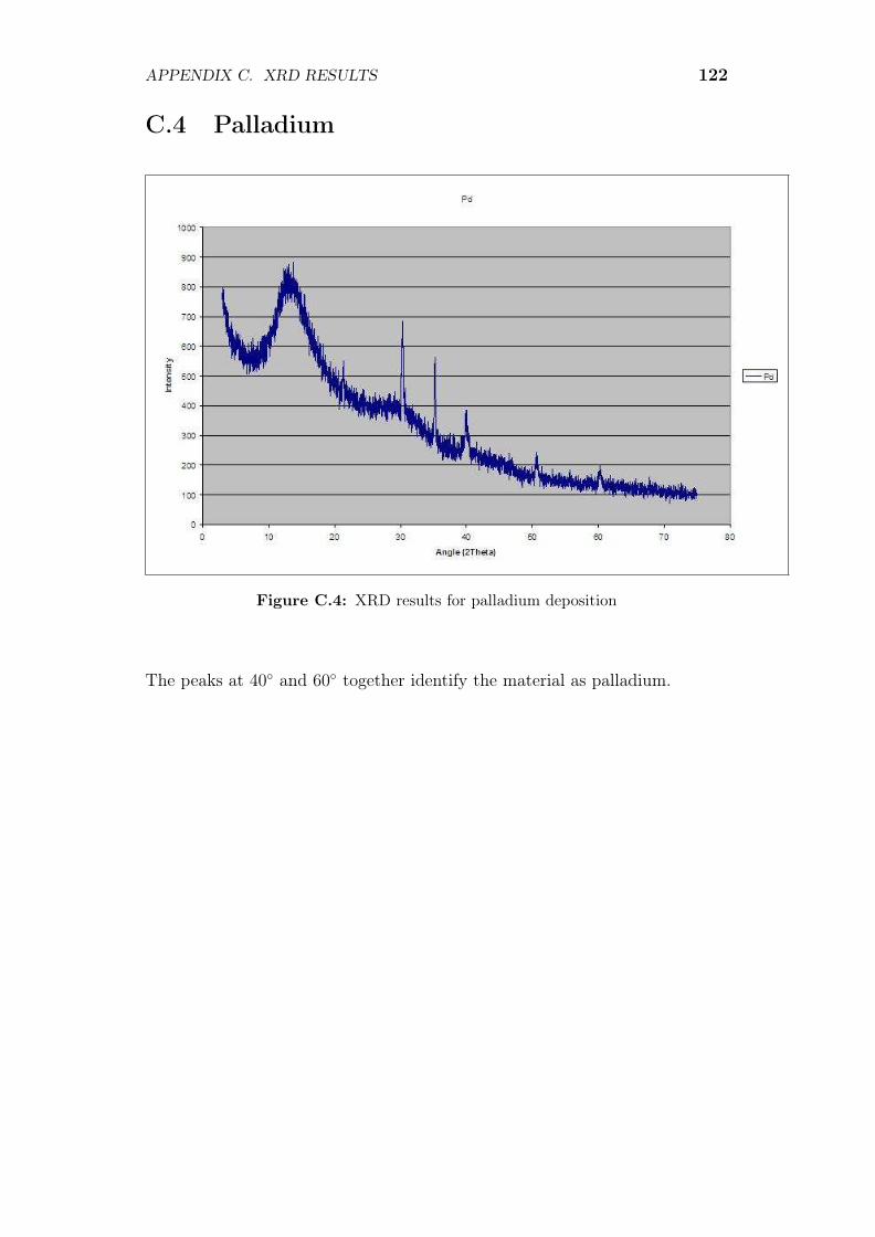
APPENDIX C. XRD RESULTS 122
C.4 Palladium
Figure C.4: XRD results for palladium deposition
The peaks at 40 and 60 together identify the material as palladium.

APPENDIX C. XRD RESULTS 123
C.5 Aluminium
Figure C.5: XRD results for aluminium deposition
The sample aluminium available in the laboratory gave this spectrum. Missingpeaks at 44 and 77, with only the 60 peak present made it impossible todefinitively identify as aluminium. Pure aluminium was therefore ordered fromSigma Aldrich.

List of References
[1] Reith, M.: Nano-Engineering in Science and Technology: An Introduction tothe World of Nano-Design. World Scientific, 2003.
[2] O.Brand, G.K.Fedder, C.Hierold, J.G.Korvink and O.Tabata: Carbon NanotubeDevices: Properties, Modeling, Integration and Applications. Wiley-VCH, 2008.
[3] Science museum. Website, July 2009.Available at: http://www.sciencemuseum.org.uk/images/I067/10328828.aspx
[4] Escutcheons of science. Website, July 2009.Available at: http://home.att.net/ numericana/arms/schickard.htm
[5] Computer history museum. Website, August 2009.Available at: http://www.computerhistory.org/collections/accession/102710252
[6] Website, August 2009.Available at: http://gadgets.boingboing.net/2008/01/
[7] Halacy, D.: Charles Babbage: Father of the Computer. Crowell-Collier Press,1970.
[8] Swade, D.: The babbage engine. Webpage, march 2009.Available at: http://www.computerhistory.org/babbage/
[9] Carol, A.: Building a calculating machine using lego® pieces. Web Article,March 2009.Available at: http://acarol.woz.org/
[10] Anthes, G.: Difference engines: The return of the mechanical computer. Webarticle, March 2008.Available at: http : //www.computerworld.com/s/article/print/313000/
DifferentEngines?taxonomyId = 12&taxonomyName = Hardware
124
LIST OF REFERENCES 125
[11] Us national nanotechnology initiative. August 2009.Available at: http://www.nano.gov/
[12] Ratner, M. and Ratner, D.: Nanotechnology: A Gentle Introduction to the NextBig Idea. Prentice Hall, 2003.
[13] Busnaina, A.: Nanomanufacturing Handbook. CRC Press, 2007.
[14] MIT: Nanomechanics links. Website, Aug 2009.Available at: web.mit.edu/cortiz/www/nanomechanics.html
[15] Answers.com. Website, October 2009.Available at: http://www.answers.com/topic/scanning-tunneling-microscope
[16] Jijmegen, R.U.: Virtual classroom biology. Website, October 2009.Available at: http://www.vcbio.science.ru.nl/en/image-gallery/electron/
[17] Greene, B.: The Elegant Universe: Superstrings, Hidden Dimensions and theQuest for the Ultimate Theory. Jonathan Cape, 1999.
[18] Drexler, K.: Nanosystems: Molecular Machinery, Manufacturing and Compu-tation. John Wiley, 1992.
[19] Madou, M.J.: Fundamentals of Microfabrication: The Science of Miniaturiza-tion. CRC Press, 2001.
[20] Pelesko, J.A.: Self Assembly: The Science of Things That Put Themselves To-gether. Chapman & Hall/CRC, 2007.
[21] The art of nano-origami. Online Article, March 2009.Available at: http://www.photonics.com/Content/ReadArticle.aspx?ArticleID=36653
[22] Mini-origami: Isi folds up tiny packages for drug delivery. Online Article, May2008.Available at: http://www3.isi.edu/about-news_story.htm?s=193
[23] Vayssieres, L.: On the design of advanced metal oxide nanomaterials. Interna-tional Journal of Nanotechnology, vol. 1, pp. 1–41, 2004.
[24] Figliola, R.S. and Beasley, D.E.: Theory and Design for Mechanical Measure-ments. John Wiley & Son, Inc., 2006.
[25] Stangroom, J. and Garvey, J.: The Great Philosophers. Arcturus Publishing,2005.

LIST OF REFERENCES 126
[26] van Ruitenbeek, J.: Silver nanoswitch. Nature, vol. 433, pp. 21–22, 2005.
[27] Terabe, K., Hasegawa, T., Nakayama, T. and Aono, M.: Quantized conductanceatomic switch. Nature, vol. 433, pp. 47–50, 2005.
[28] Li, X.X.L., Yu, G., Di, C.-A., Wei, D., Ye, S. and Liuc, Y.: Nanophotoswitcheswith a high on/off ratiobased on a structure of indium tin oxide/organic insu-lator/metal. Applied Physics Letters to nature, vol. 92, pp. 043302: 1–3, 2008.
[29] Tang, Q., Li, L., Song, Y., Liu, Y., Li, H., Xu, W., Liu, Y., Hu, W., andZhu, D.: Photoswitches and phototransistors from organic single-crystallinesub-micro/nanometer ribbons. Advanced Materials, vol. 19, pp. 2624–2628,2007.
[30] Benedetto, F.D., Mele, E., Camposeo, A., Athanassiou, A., Cingolani, R. andPisignano, D.: Photoswitchable organic nanofibers. Advanced Materials, vol. 20,pp. 314–318, 2008.
[31] Lee, S.W.L.D.S., Morjan, R.E., Jhang, S.H., Sveningsson, M., Nerushev, O.,Park, Y.W. and Campell, E.E.: A three-terminal carbon nanorelay. Nano Let-ters, vol. 4, no. 10, pp. 2027–2030, 2004.
[32] O’Connell, M.J. (ed.): Carbon Nanotubes: Properties and Applications. CRCPress/Taylor & Fancis Group, 2006.
[33] Kaul, A.B., Wong, E.W., Epp, L. and Hunt, B.D.: Electromechanical carbonnanotube switches for high-frequency applications. Nano Letters to nature,vol. 6, pp. 942–947, 2006.
[34] Deshpande, V., Chiu, H.-Y., Postma, H., Miko, C., Forro, L. and Bockrath,M.: Carbon nanotube linear bearing nanoswitches. Nano Letters, vol. 6, pp.1092–1095, 2006.
[35] PuYang, F., Xu, H., Ho, C.-M., Liu, Y., Flood, A.H., Bonvallet, P.A., Tseng,H.-R., Stoddart, J.F., Baller, M. and Magonov, S.: All-carbon nanoswitch basedon molecule: a first principles study. Journal of Applied Physics, vol. 102, pp.064501: 1–4, 2007.
[36] Tsunani, N.: A v6 engine for the nano-age. Website, August 2009.Available at: http://www.voyle.net/Nano%20Research-05-100+/research-05-0106.htm
[37] Kourens, A.: Wetenskaplike Skryfvaardighede: Riglyne vir die skryf van tesisseen proefskrifte. Sun Press, 2004.
LIST OF REFERENCES 127
[38] Laboratories, C.: A basic introduction to clean rooms. Website, February 2009.Available at: http://www.coastwidelabs.com/Technical%20Articles/Cleaning%20the%20Cleanroom.htm
[39] Ullman, D.G.: The Mechanical Design Process. McGraw Hill, 2003.
[40] Konenkamp, R., Word, R.C. and Godinez, M.: Ultraviolet electroluminescencefrom zno/polymer heterojunction light-emitting diodes. Nano Letters, vol. 5,pp. 2005–2008, 2005.
[41] Abramson, A.R.: Thermal Energy Transport in Micro/Nanostructures. Ph.D.thesis, University of California, Berkley, 2002.
[42] Bedair, S.S. and Fedder, G.K.: The 13th international conference on solid-state sensors, actuators and microsystems. In: Polymer Wicking to Mass LoadCantilever for Chemical Gravimetric Sensors. 2005.
[43] ta Wang, C. and chern Yen, S.: Theoretical analysis of film uniformity in spin-ning processes. Chemical Engineering Science, vol. 50, pp. 989–999, 1995.
[44] TOXICOLOGICAL PROFILE FOR TOLUENE U.S. DEPARTMENT OFHEALTH AND HUMAN SERVICES Public Health Service Agency for ToxicSubstances and Disease Registry, 2000.Available at: http://www.atsdr.cdc.gov/toxprofiles/tp56.pdf
[45] PUBLIC HEALTH STATEMENT Xylene, 2007.Available at: http://www.atsdr.cdc.gov/toxprofiles/tp71-c1-b.pdf
[46] Press, B.: Ganoskin. Website, July 2009.Available at: http://www.ganoksin.com/borisat/nenam/nillo-work-10-1.htm
[47] Wood, A.: Alan wood’s web site. Website, May 2009.Available at: www.alanwood.net/pesticides/calciumpolysulfid.html
[48] Chorkendorff, I. and Niemantsverdriet, J.: Concepts of Modern Cartalysis andKinetics. Wiley-VCH, 2003.
[49] Co., K.J.: Materials guide for thermal evaporation. Pdf Guide, August 2008.Available at: http : //www.lesker.com/newweb/menuevapsources.cfm?CFID
=180535&CFTOKEN=48466901§ion=materialdeptable&init= skip
[50] Ramezani, A., Alasty, A. and Akbari, J.: Closed-form solutions of the pull-in instability in nano-cantilevers under electrostatic and intermolecular surface

LIST OF REFERENCES 128
forces. International Journal of Solids and Structures, vol. 44, pp. 4925–4941,2007.
[51] Tang, Z., Xu, Y., Li, G. and Aluru, N.: Physical models for coupled electrome-chanical analysis of silicon nanoelectromechanical systems. Journal of AppliedPhysics, vol. 97, pp. 114304: 1–13, 2005.
[52] E.Shigley, J., Mischke, C.R. and Budynas, R.G.: Mechanical Engineering De-sign. McGraw Hill, 2004.
[53] Yang, J., Jia, X. and Kitipornchai, S.: Pull-in instability of nanoswitches us-ing nonlocal elasticity theory. Journal of Applied Physics D: Applied Physics,vol. 41, pp. 1–8, 2008.