an introduction to verilog - pages.hmc.edupages.hmc.edu/harris/class/e155/04/verilog.pdf4 modeling...
TRANSCRIPT
1
An Introduction to Verilog David Harris
August 20, 2002
Table of Contents
1 Introduction ............................................................................................................................................ 2 2 Modeling with Continuous Assignments................................................................................................ 2
2.1 Bitwise Operators ........................................................................................................................... 2 2.2 Comments & White Space.............................................................................................................. 3 2.3 Reduction Operators ....................................................................................................................... 3 2.4 Other Operators .............................................................................................................................. 3
3 Useful Constructs ................................................................................................................................... 4 3.1 Internal Signals ............................................................................................................................... 4 3.2 Precedence ...................................................................................................................................... 4 3.3 Constants ........................................................................................................................................ 5 3.4 Hierarchy ........................................................................................................................................ 5 3.5 Tristates .......................................................................................................................................... 5 3.6 Bit Swizzling .................................................................................................................................. 6
4 Modeling with Always Blocks ............................................................................................................. 7 4.1 Flip-Flops........................................................................................................................................ 7 4.2 Latches............................................................................................................................................ 8 4.3 Counters.......................................................................................................................................... 9 4.4 Combinational Logic .................................................................................................................... 10 4.5 Memories ...................................................................................................................................... 13 4.6 Blocking and Nonblocking Assignment ....................................................................................... 14
5 Finite State Machines ........................................................................................................................... 16 6 Test Benches......................................................................................................................................... 20 7 Verilog Style Guidelines....................................................................................................................... 22
7.1 General Guidelines ....................................................................................................................... 22 7.2 Xilinx Hints .................................................................................................................................. 23
8 Bad Circuit Examples ........................................................................................................................... 23 8.1 Incorrect stimulus list ................................................................................................................... 23 8.2 Missing begin/end block............................................................................................................... 24 8.3 Undefined Outputs........................................................................................................................ 25 8.4 Incomplete Specification of Cases................................................................................................ 26 8.5 Shorted Outputs ............................................................................................................................ 29
2
1 Introduction These notes give a quick introduction to the Verilog Hardware Description Language (HDL). There are many texts on Verilog (e.g. [Smith00], [Ciletti99], etc.) providing a more in-depth treatment and the IEEE standard itself is quite readable as well as authoritative [IEEE1364-01]. Many books treat Verilog as a programming language, which is not the best way of viewing it. Instead, Verilog is better understood as a shorthand for describing digital hardware. In other words, begin your design process by planning, on paper or in your mind, the hardware you want. For example, the MIPS processor consists of a FSM controller and a datapath built from registers, adders, multiplexers, etc. Then write Verilog that implies that hardware to a synthesis tool. A common error among beginners is to instead write a program without thinking about the hardware that is implied. If you don’t know what hardware you are implying, you are almost certain to get something that you didn’t want. Sometimes this means extra latches appearing in your circuit in places you didn’t expect. Other times, it means that the circuit is much slower than required or takes far more gates than it would if more carefully described. The Verilog language was developed by Gateway Design Automation as a proprietary language for logic simulation in 1984. Gateway was acquired by Cadence in 1989 and Verilog was made an open standard in 1990 under the control of Open Verilog International. The language, with some revisions, became an IEEE standard in 1995 and was updated in 2001. This appendix describes a style compatible with both the 1995 and 2001 standards. There are two general styles of description: behavioral and structural. Structural Verilog describes how a module is composed of simpler modules or of basic primitives such as gates or transistors. Behavioral Verilog describes how the outputs are computed as functions of the inputs. There are two general types of statements used in behavioral Verilog. Continuous assignment statements always imply combinational logic. Always blocks can imply combinational logic or sequential logic, depending how they are used. It is critical to partition your design into combinational and sequential components and write Verilog in such a way that you get what you want. If you don’t know whether a block of logic is combinational or sequential, you are very likely to get the wrong thing. .
2 Modeling with Continuous Assignments With schematics, a 32-bit adder is a complex design. It can be constructed from 32 full adder cells, each of which in turn requires about six 2-input gates. Verilog provides a much more compact description:
module adder(a, b, y); input [31:0] a, b; output [31:0] y; assign y = a + b; endmodule
A Verilog module is like a “cell” or “macro” in schematics. It begins with a description of the inputs and outputs, which in this case are 32 bit busses. In the structural description style, the module may contain assign statements, always blocks, or calls to other modules. During simulation, an assign statement causes the left hand side (y) to be updated any time the right side (a/b) changes. This necessarily implies combinational logic; the output on the left side is a function of the current inputs given on the right side. A 32-bit adder is a good example of combinational logic.
2.1 Bitwise Operators Verilog has a number of bitwise operators that act on busses. For example, the following module describes four inverters.
3
module inv(a, y); input [3:0] a; output [3:0] y; assign y = ~a; endmodule
Similar bitwise operations are available for the other basic logic functions:
module gates(a, b, y1, y2, y3, y4, y5); input [3:0] a, b; output [3:0] y1, y2, y3, y4, y5; /* Five different two-input logic gates acting on 4 bit busses */ assign y1 = a & b; // AND assign y2 = a | b; // OR assign y3 = a ^ b; // XOR assign y4 = ~(a & b); // NAND assign y5 = ~(a | b); // NOR endmodule
2.2 Comments & White Space The previous examples showed two styles of comments, just like those used in C or Java. Comments beginning with /* continue, possibly across multiple lines, to the next */. Comments beginning with // continue to the end of the line. It is important to properly comment complex logic so you can understand what you did six months from now or so that some poor slob assigned to fix your buggy code will be able to figure it out rather than calling you at 2 am with a question. Verilog is not picky about the use of white space. Nevertheless, proper indenting and spacing is very helpful to make nontrivial designs readable. Verilog is case-sensitive. Be consistent in your use of capitalization and underscores in signal and module names.
2.3 Reduction Operators Reduction operators imply a multiple-input gate acting on a single bus. For example, the following module describes an 8-input AND gate with inputs A[0], A[1], A[2], …, A[7].
module and8(a, y); input [7:0] a; output y; assign y = &a; endmodule
As one would expect, |, ^, ~&, and ~| reduction operators are available for OR, XOR, NAND, and NOR as well. Recall that a multi-bit XOR performs parity, returning true if an odd number of inputs are true.
2.4 Other Operators The conditional operator ?: works like the same operator in C or Java and is very useful for describing multiplexers. It is called a ternary operator because it takes three inputs. If the first input is nonzero, the result is the expression in the second input. Otherwise, the result is the expression in the third input.
4
module mux2(d0, d1, s, y); input [3:0] d0, d1; input s; output [3:0] y; assign y = s ? d1 : d0; // if s=1, y=d1, else y=d0 endmodule
A number of arithmetic functions are supported including +, -, *, <, >, <=, >=, = =, !=, <<, >>, / and %. Recall from other languages that % is the modulo operator: a%b equals the remainder of a when divided by b. These operations imply a vast amount of hardware. = = and != (equality / inequality) on N-bit inputs require N 2-input XNORs to determine equality of each bit and an N-input AND or NAND to combine all the bits. Addition, subtraction, and comparison all require an adder, which is very expensive in hardware. Variable left and right shifts << and >> imply a barrel shifter. Multipliers are even more costly. Do not use these statements without contemplating the number of gates you are generating. Moreover, the implementations are not always particularly efficient for your problem. You’ll probably be disappointed with the speed and gate count of a multiplier your synthesis tool produces from when it sees *. You’ll be better off writing your own Booth-encoded multiplier if these constraints matter. Many synthesis tools choke on / and % because these are nontrivial functions to implement in combinational logic.
3 Useful Constructs
3.1 Internal Signals Often it is convenient to break a complex calculation into intermediate variables. For example, in a full adder, we sometimes define the propagate signal as the XOR of the two inputs A and B. The sum from the adder is the XOR of the propagate signal and the carry in. We can name the propagate signal using a wire statement, in much the same way we use local variables in a programming language.
module fulladder(a, b, cin, s, cout); input a, b, cin; output s, cout; wire prop; assign prop = a ^ b; assign s = prop ^ cin; assign cout = (a & b) | (cin & (a | b)); endmodule
Technically, it is not necessary to declare single-bit wires. However, it is necessary to declare multi-bit busses. It is good practice to declare all signals. Some Verilog simulation and synthesis tools give errors that are difficult to decipher when a wire is not declared.
3.2 Precedence Notice that we fully parenthesized the cout computation. We could take advantage of operator precedence to use fewer parentheses:
assign cout = a&b | cin&(a|b) The operator precedence from highest to lowest is much as you would expect in other languages. AND has precedence over OR.
5
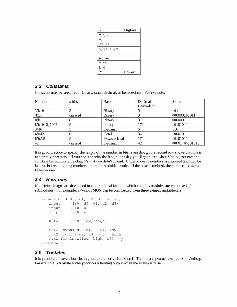
~ Highest *, /, % +, - <<, >> <, <=, >, >= =, = =, != &, ~& ^, ~^ |, ~| ?: Lowest
3.3 Constants Constants may be specified in binary, octal, decimal, or hexadecimal. For example: Number # bits Base Decimal
Equivalent Stored
3’b101 3 Binary 5 101 ’b11 unsized Binary 3 000000..00011 8’b11 8 Binary 3 00000011 8’b1010_1011 8 binary 171 10101011 3’d6 3 Decimal 6 110 6’o42 6 Octal 34 100010 8’hAB 8 Hexadecimal 171 10101011 42 unsized Decimal 42 0000…00101010 It is good practice to specify the length of the number in bits, even though the second row shows that this is not strictly necessary. If you don’t specify the length, one day you’ll get bitten when Verilog assumes the constant has additional leading 0’s that you didn’t intend. Underscores in numbers are ignored and may be helpful in breaking long numbers into more readable chunks. If the base is omitted, the number is assumed to be decimal.
3.4 Hierarchy Nontrivial designs are developed in a hierarchical form, in which complex modules are composed of submodules. For example, a 4-input MUX can be constructed from three 2-input multiplexers:
module mux4(d0, d1, d2, d3, s, y); input [3:0] d0, d1, d2, d3; input [1:0] s; output [3:0] y; wire [3:0] low, high; mux2 lowmux(d0, d1, s[0], low); mux2 highmux(d2, d3, s[0], high); mux2 finalmux(low, high, s[1], y); endmodule
3.5 Tristates It is possible to leave a bus floating rather than drive it to 0 or 1. This floating value is called ’z in Verilog. For example, a tri-state buffer produces a floating output when the enable is false.

6
module tristate(a, en, y); input [3:0] a; input en; output [3:0] y; assign y = en ? a : 4’bz; endmodule
Floating inputs to gates cause undefined outputs, displayed as ’x in Verilog. At startup, state nodes such as the internal node of flip-flops are also usually initialized to ’x, as we will see later. We could define a multiplexer using two tristates so that the output is always driven by exactly one tristate. This guarantees there are no floating nodes.
module mux2(d0, d1, s, y); input [3:0] d0, d1; input s; output [3:0] y; tristate t0(d0, ~s, y); tristate t1(d1, s, y); endmodule
3.6 Bit Swizzling Often it is necessary to work on parts of a bus or to concatenate (join together) signals to construct busses. The previous example showed using the least significant bit s[0] of a 2-bit select signal for some muxes and the most significant bit s[1] for the final mux. Use ranges to select subsets of a bus. For example, an 8-bit wide 2-input mux can be constructed from two 4-bit wide 2-input muxes:
module mux2_8(d0, d1, s, y); input [7:0] d0, d1; input s; output [7:0] y; mux2 lsbmux(d0[3:0], d1[3:0], s, y[3:0]); mux2 msbmux(d0[7:4], d1[7:4], s, y[7:4]); endmodule
The {} notation is used to concatenate busses. For example, the following 8x8 multiplier produces a 16-bit result, which is, placed on the upper and lower 8-bit result busses.
module mul(a, b, upper, lower); input [7:0] a, b; output [7:0] upper, lower; assign {upper, lower} = a*b; endmodule
A 16-bit 2’s complement number is sign-extended to 32-bits by copying the most significant bit to each of the upper 16 positions. The Verilog syntax concatenates 16 copies of a[15] to the 16-bit a[15:0] bus. You will get a warning from synthesis that a is a “feedthrough net.” This means that the input “feeds through” to the output. y[15:0] should have the same value as a[15:0], so this is what we intended. If you get a feedthrough net warning where you did not intend a feedthrough, check for a mistake in your Verilog.
7
module signextend(a, y); input [15:0] a; output [31:0] y; assign y = {16{a[15]}, a[15:0]}; endmodule
The next statement generates a bizarre combination of two busses. Don’t confuse the 3-bit binary constant 3’b101 with bus b. Note that it was important to specify the length of 3 bits in the constant; otherwise many additional 0’s might have appeared in the middle of y.
assign y = {a[2:1], 3{b[0]}, a[0], 3’b101, b[1:3]}
a[2] a[1] b[0] b[0] b[0] a[0] 1 0 1y = b[1] b[2] b[3]
4 Modeling with Always Blocks Assign statements are reevaluated every time any term on the right hand side changes. Therefore, they must describe combinational logic. Always blocks are reevaluated only when signals in the header change. Depending on the form, always blocks may imply sequential or combinational circuits.
4.1 Flip-Flops Flip-flops are described with an always @(posedge clk) statement:
module flop(clk, d, q); input clk; input [3:0] d; output [3:0] q; reg [3:0] q; always @(posedge clk) q <= d; endmodule
The body of the always statement is only evaluated on the rising (positive) edge of the clock. At this time, the output q is copied from the input d. The <= is called a nonblocking assignment. Think of it as a regular equals sign for now; we’ll return to the subtle points later. Notice that it is used instead of assign inside the always block. All the signals on the left hand side of assignments in always blocks must be declared as reg. This is a confusing point for new Verilog users. In this circuit, q is also the output. Declaring a signal as reg does not mean the signal is actually a register! All it means is it appears on the left side in an always block. We will see examples of combinational signals later that are declared reg but have no flip-flops. At startup, the q output is initialized to ’x. Generally, it is good practice to use flip-flops with reset inputs so that on power-up you can put your system in a known state. The reset may be either asynchronous or synchronous. Asynchronous resets occur immediately. Synchronous resets only change the output on the rising edge of the clock. Xilinx FPGAs have dedicated internal hardware to support initializing asynchronously resettable flip-flops on startup, so such flops are preferred.

8
module flopr(clk, reset, d, q); // asynchronous reset input clk; input reset; input [3:0] d; output [3:0] q; reg [3:0] q; always @(posedge clk or posedge reset) if (reset) q <= 4’b0; else q <= d; endmodule
module flopr(clk, reset, d, q); // synchronous reset input clk; input reset; input [3:0] d; output [3:0] q; reg [3:0] q; always @(posedge clk) if (reset) q <= 4’b0; else q <= d; endmodule
Note that the asynchronously resettable flop evaluates the always block when either clk or reset rise so that it immediately responds to reset. The synchronously reset flop is not sensitized to reset in the @ list, so it waits for the next clock edge before clearing the output. One could also consider flip-flops with enables that only load the input when the enable is true. The following flip-flop retains its old value if both reset and en are false.
module flopenr(clk, reset, en, d, q); // asynchronous reset input clk; input reset; input en; input [3:0] d; output [3:0] q; reg [3:0] q; always @(posedge clk or posedge reset) if (reset) q <= 4’b0; else if (en) q <= d; endmodule
4.2 Latches Always blocks can also be used to model transparent latches, also known as D latches. When the clock is high, the latch is transparent and the data input flows to the output. When the clock is low, the latch goes opaque and the output remains constant.
9
module latch(clk, d, q); input clk; input [3:0] d; output [3:0] q; reg [3:0] q; always @(clk or d) if (clk) q <= d; endmodule
The latch evaluates the always block any time either clk or d change. If the clock is high, the output gets the input. Notice that even though q is a latch node, not a register node, it is still declared as reg because it is on the left hand side of a <= in an always block. Most Xilinx FPGAs do not support latches very well. If your code includes latches either intentionally or by accident, you will get a warning about “latch inferred in design” and should remove them.
4.3 Counters Consider two ways of describing a four-bit counter with asynchronous reset. The first scheme implies a sequential circuit containing both the 4-bit flip-flop and an adder. The second scheme explicitly declares modules for the flip-flop and adder. Either scheme is good for a simple circuit such as a counter. As you develop more complex finite state machines, it is a good idea to separate the next state logic from the flip-flops in your Verilog code. Verilog does not protect you from yourself here and there are many simple errors that lead to circuits very different than you intended.
module counter(clk, reset, q); input clk; input reset; output [3:0] q; reg [3:0] q;
// counter using always block
always @(posedge clk) if (reset) q <= 4’b0; else q <= q+1; endmodule
module counter(clk, reset, q); input clk; input reset; output [3:0] q; wire [3:0] nextq;
// counter using module calls
flopr qflop(clk, reset, nextq, q); adder inc(q, 4’b0001, nextq); // assumes a 4-bit adder endmodule
10
4.4 Combinational Logic Always blocks imply sequential logic when some of the inputs do not appear in the @ stimulus list or might not cause the output to change. For example, in the flop module, d is not in the @ list, so the flop does not immediately respond to changes of d. In the latch, d is in the @ list, but changes in d are ignored unless clk is high. Always blocks can also be used to imply combinational logic if they are written in such a way that the output always is reevaluated given changes in any of the inputs. The following code shows how to define a bank of inverters with an always block.
module inv(a, y); input [3:0] a; output [3:0] y; reg [3:0] y; always @(a) y <= ~a; endmodule
Similarly, the next example defines a 5 banks of different kinds of gates. Notice that the begin / end construct is necessary because multiple commands appear in the always block. This is analogous to { } block structure in C or Java. The begin / end was not needed in the flopr example because an if / else command counts as a single statement.
module gates(a, b, y1, y2, y3, y4, y5); input [3:0] a, b; output [3:0] y1, y2, y3, y4, y5; reg [3:0] y1, y2, y3, y4, y5; always @(a or b) begin y1 <= a & b; // AND y2 <= a | b; // OR y3 <= a ^ b; // XOR y4 <= ~(a & b); // NAND y5 <= ~(a | b); // NOR end endmodule
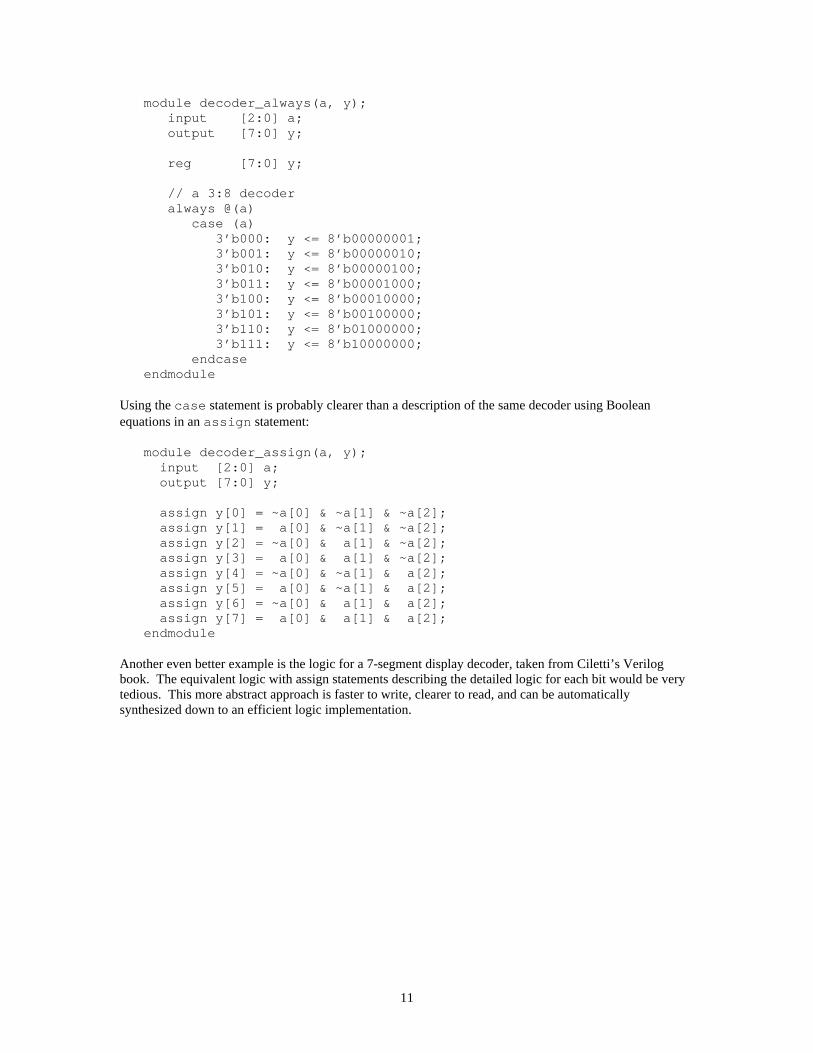
These two examples are poor applications of always blocks for modeling combinational logic because they require more lines than the equivalent approach with assign statements as well as posing the risk of inadvertently implying sequential logic (see the bad circuit examples later). A better application of the always block is a decoder, which takes advantage of the case statement that may only appear inside an always block.
11
module decoder_always(a, y); input [2:0] a; output [7:0] y; reg [7:0] y; // a 3:8 decoder always @(a) case (a) 3’b000: y <= 8’b00000001; 3’b001: y <= 8’b00000010; 3’b010: y <= 8’b00000100; 3’b011: y <= 8’b00001000; 3’b100: y <= 8’b00010000; 3’b101: y <= 8’b00100000; 3’b110: y <= 8’b01000000; 3’b111: y <= 8’b10000000; endcase endmodule
Using the case statement is probably clearer than a description of the same decoder using Boolean equations in an assign statement:
module decoder_assign(a, y); input [2:0] a; output [7:0] y; assign y[0] = ~a[0] & ~a[1] & ~a[2]; assign y[1] = a[0] & ~a[1] & ~a[2]; assign y[2] = ~a[0] & a[1] & ~a[2]; assign y[3] = a[0] & a[1] & ~a[2]; assign y[4] = ~a[0] & ~a[1] & a[2]; assign y[5] = a[0] & ~a[1] & a[2]; assign y[6] = ~a[0] & a[1] & a[2]; assign y[7] = a[0] & a[1] & a[2]; endmodule
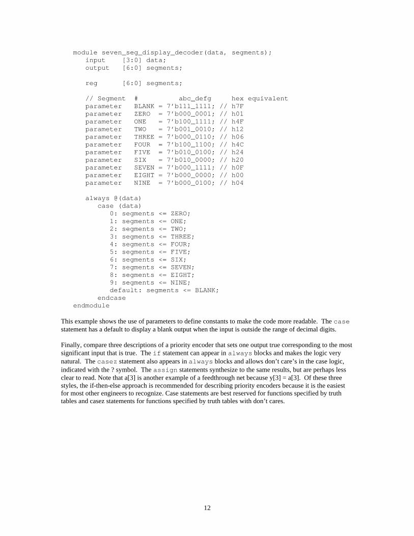
Another even better example is the logic for a 7-segment display decoder, taken from Ciletti’s Verilog book. The equivalent logic with assign statements describing the detailed logic for each bit would be very tedious. This more abstract approach is faster to write, clearer to read, and can be automatically synthesized down to an efficient logic implementation.
12
module seven_seg_display_decoder(data, segments); input [3:0] data; output [6:0] segments; reg [6:0] segments; // Segment # abc_defg hex equivalent parameter BLANK = 7’b111_1111; // h7F parameter ZERO = 7’b000_0001; // h01 parameter ONE = 7’b100_1111; // h4F parameter TWO = 7’b001_0010; // h12 parameter THREE = 7’b000_0110; // h06 parameter FOUR = 7’b100_1100; // h4C parameter FIVE = 7’b010_0100; // h24 parameter SIX = 7’b010_0000; // h20 parameter SEVEN = 7’b000_1111; // h0F parameter EIGHT = 7’b000_0000; // h00 parameter NINE = 7’b000_0100; // h04 always @(data) case (data) 0: segments <= ZERO; 1: segments <= ONE; 2: segments <= TWO; 3: segments <= THREE; 4: segments <= FOUR; 5: segments <= FIVE; 6: segments <= SIX; 7: segments <= SEVEN; 8: segments <= EIGHT; 9: segments <= NINE; default: segments <= BLANK; endcase endmodule
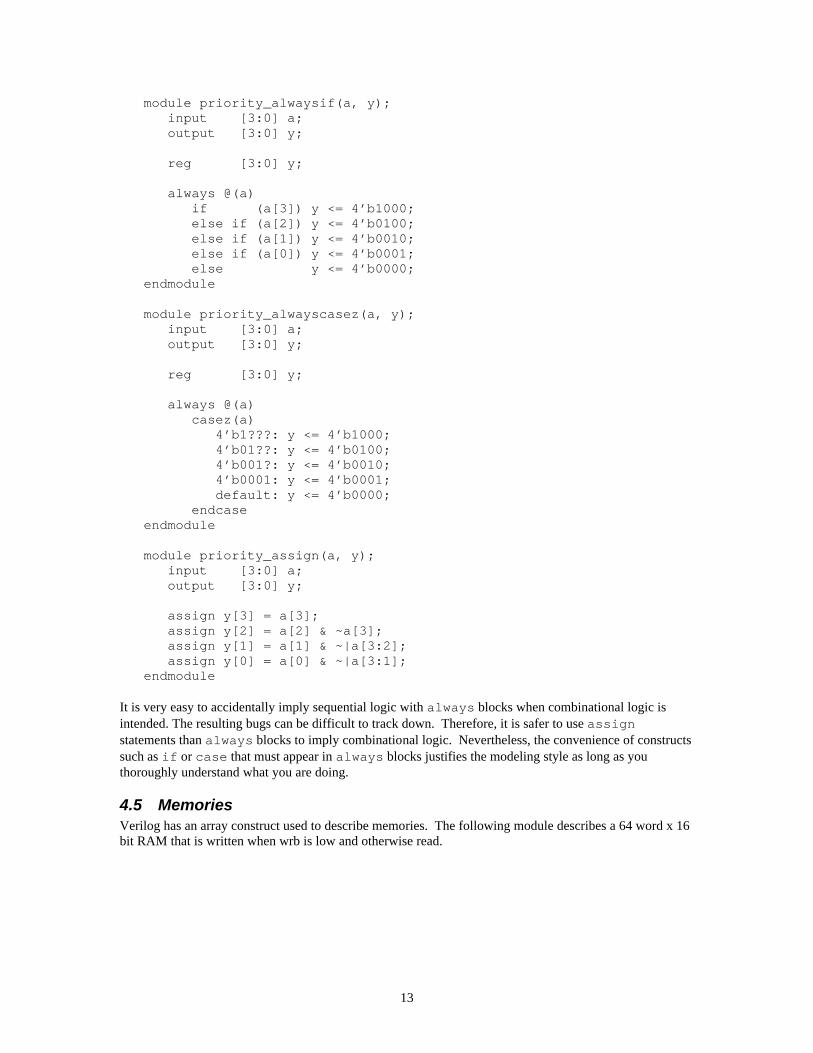
This example shows the use of parameters to define constants to make the code more readable. The case statement has a default to display a blank output when the input is outside the range of decimal digits. Finally, compare three descriptions of a priority encoder that sets one output true corresponding to the most significant input that is true. The if statement can appear in always blocks and makes the logic very natural. The casez statement also appears in always blocks and allows don’t care’s in the case logic, indicated with the ? symbol. The assign statements synthesize to the same results, but are perhaps less clear to read. Note that a[3] is another example of a feedthrough net because y[3] = a[3]. Of these three styles, the if-then-else approach is recommended for describing priority encoders because it is the easiest for most other engineers to recognize. Case statements are best reserved for functions specified by truth tables and casez statements for functions specified by truth tables with don’t cares.
13
module priority_alwaysif(a, y); input [3:0] a; output [3:0] y; reg [3:0] y; always @(a) if (a[3]) y <= 4’b1000; else if (a[2]) y <= 4’b0100; else if (a[1]) y <= 4’b0010; else if (a[0]) y <= 4’b0001; else y <= 4’b0000; endmodule
module priority_alwayscasez(a, y); input [3:0] a; output [3:0] y; reg [3:0] y; always @(a) casez(a) 4’b1???: y <= 4’b1000; 4’b01??: y <= 4’b0100; 4’b001?: y <= 4’b0010; 4’b0001: y <= 4’b0001; default: y <= 4’b0000; endcase endmodule
module priority_assign(a, y); input [3:0] a; output [3:0] y; assign y[3] = a[3]; assign y[2] = a[2] & ~a[3]; assign y[1] = a[1] & ~|a[3:2]; assign y[0] = a[0] & ~|a[3:1]; endmodule
It is very easy to accidentally imply sequential logic with always blocks when combinational logic is intended. The resulting bugs can be difficult to track down. Therefore, it is safer to use assign statements than always blocks to imply combinational logic. Nevertheless, the convenience of constructs such as if or case that must appear in always blocks justifies the modeling style as long as you thoroughly understand what you are doing.
4.5 Memories Verilog has an array construct used to describe memories. The following module describes a 64 word x 16 bit RAM that is written when wrb is low and otherwise read.

14
module ram(addr, wrb, din, dout); input [5:0] addr; input wrb; input [15:0] din; output [15:0] dout; reg [15:0] mem[63:0]; // the memory reg [15:0] dout; always @(addr or wrb or din) if (~wrb) mem[addr] <= din; else dout <= mem[addr]; endmodule
FPGAs have a limited number of bits of RAM on board. Large memories are extremely expensive. In the Xilinx Foundation tools, it is more efficient to specify a RAM or ROM using the LogiBLOX tool.
4.6 Blocking and Nonblocking Assignment Verilog supports two types of assignments inside an always block. Blocking assignments use the = statement. Nonblocking assignments use the <= statement. Do not confuse either type with the assign statement, which cannot appear inside always blocks at all. A group of blocking assignments inside a begin/end block are evaluated sequentially, just as one would expect in a standard programming language. A group of nonblocking assignments are evaluated in parallel; all of the statements are evaluated before any of the left hand sides are updated. This is what one would expect in hardware because real logic gates all operate independently rather than waiting for the completion of other gates. For example, consider two attempts to describe a shift register. On each clock edge, the data at sin should be shifted into the first flop. The first flop shifts to the second flop. The data in the second flop shifts to the third flop, and so on until the last element drops off the end.
clk
sin
q[0] q[1] q[2] q[3]
Intended Shift Register

15
module shiftreg(clk, sin, q); input clk; input sin; output [3:0] q; // This is a correct implementation using nonblocking assignment reg [3:0] q; always @(posedge clk) begin q[0] <= sin; // <= indicates nonblocking assignment q[1] <= q[0]; q[2] <= q[1]; q[3] <= q[2]; // it would be even more better to write q <= {q[2:0], sin}; end endmodule
The nonblocking assignments mean that all of the values on the right hand sides are assigned simultaneously. Therefore, q[1] will get the original value of q[0], not the value of sin that gets loaded into q[0]. This is what we would expect from real hardware. Of course all of this could be written on one line for brevity. Blocking assignments are more familiar from traditional programming languages, but inaccurately model hardware. Consider the same module using blocking assignments. When clk rises, the Verilog says that q[0] should be copied from sin. Then q[1] should be copied from the new value of q[0] and so forth. All four registers immediately get the sin value.
module shiftreg(clk, sin, q[3:0]); input clk; input sin; output [3:0] q; // This is a bad implementation using blocking assignment reg [3:0] q; always @(posedge clk) begin q[0] = sin; // = indicates blocking assignment q[1] = q[0]; q[2] = q[1]; q[3] = q[2]; end endmodule
The moral of this illustration is to always use nonblocking assignment in always blocks when writing structural Verilog. With sufficient cleverness, such as reversing the orders of the four commands, one might make blocking assignments work correctly, but they offer no advantages and great risks. Finally, note that each always block implies a separate block of logic. Therefore, a given reg may be assigned in only one always block. Otherwise, two pieces of hardware with shorted outputs would be implied.
16
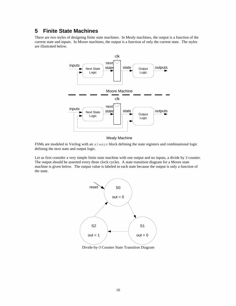
5 Finite State Machines There are two styles of designing finite state machines. In Mealy machines, the output is a function of the current state and inputs. In Moore machines, the output is a function of only the current state. The styles are illustrated below.
OutputLogic
Next StateLogic
clk
state outputsinputsnextstate
Moore Machine
OutputLogic
Next StateLogic
clk
state outputsinputs nextstate
Mealy Machine
FSMs are modeled in Verilog with an always block defining the state registers and combinational logic defining the next state and output logic. Let us first consider a very simple finite state machine with one output and no inputs, a divide by 3 counter. The output should be asserted every three clock cycles. A state transition diagram for a Moore state machine is given below. The output value is labeled in each state because the output is only a function of the state.
S2
out = 1
S1
out = 0
S0
out = 0
reset
Divide-by-3 Counter State Transition Diagram

17
module divideby3FSM(clk, reset, out); input clk; input reset; output out; reg [1:0] state; reg [1:0] nextstate; parameter S0 = 2’b00; parameter S1 = 2’b01; parameter S2 = 2’b10; // State Register always @(posedge clk or posedge reset) if (reset) state <= S0; else state <= nextstate; // Next State Logic always @(state) case (state) S0: nextstate <= S1; S1: nextstate <= S2; S2: nextstate <= S0; default: nextstate <= S0; endcase // Output Logic assign out = (state == S2); endmodule
The FSM model is divided into three portions: the state register, next state logic, and output logic. The state logic describes an asynchronously resettable flip-flop that resets to an initial state and otherwise advances to the computed next state. Defining states with parameters allows the easy modification of state encodings and makes the code easier to read. The next state logic computes the next state as a function of the current state and inputs; in this example there are no inputs. A case statement in an always @(state or inputs) block is a convenient way to define the next state. It is important to have a default if not all cases are enumerated; otherwise the nextstate would not be assigned in the undefined cases. This implies that nextstate should keep its old value, which would require the existence of latches. Finally, the output logic may be a function of the current state alone in a Moore machine or of the current state and inputs in a Mealy machine. Depending on the complexity of the design, assign statements, if statements, or case statements may be most readable and efficient. The next example shows a finite state machine with an input A and two outputs. Output X is true when the input is the same now as it was last cycle. Output Y is true when the input is the same now as it was for the past two cycles. This is a Mealy machine because the output depends on the current inputs as well as the state. The outputs are labeled on each transition after the input. The state transition diagram is shown below:
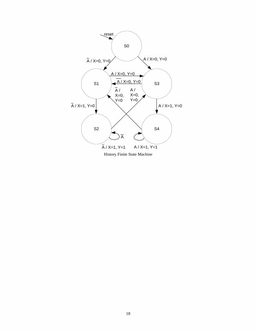
18
S1 S3
S2 S4
S0
reset
A / X=0, Y=0
A
A / X=1, Y=0
A / X=1, Y=1
A /X=0,Y=0
A /X=0,Y=0
A / X=0, Y=0
A / X=1, Y=0
A / X=1, Y=1
A / X=0, Y=0
A / X=0, Y=0
History Finite State Machine

19
module historyFSM(clk, reset, a, x, y); input clk; input reset; input a; output x, y; reg [2:0] state; reg [2:0] nextstate; parameter S0 = 3’b000; parameter S1 = 3’b010; parameter S2 = 3’b011; parameter S3 = 3’b100; parameter S4 = 3’b101; // State Register always @(posedge clk or posedge reset) if (reset) state <= S0; else state <= nextstate; // Next State Logic always @(state or a) case (state) S0: if (a) nextstate <= S3; else nextstate <= S1; S1: if (a) nextstate <= S3; else nextstate <= S2; S2: if (a) nextstate <= S3; else nextstate <= S2; S3: if (a) nextstate <= S4; else nextstate <= S1; S4: if (a) nextstate <= S4; else nextstate <= S1; default: nextstate <= S0; endcase // Output Logic assign x = (state[1] & ~a) | (state[2] & a); assign y = (state[1] & state[0] & ~a) | (state[2] & state[0] & a); endmodule
The output logic equations depend on the specific state encoding and were worked out by hand. A more general approach is independent of the encodings and requires less thinking, but might require more gates and code:
20
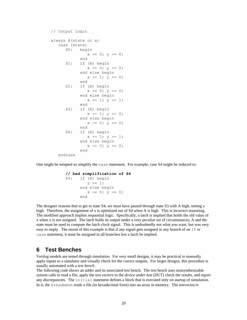
// Output Logic always @(state or a) case (state) S0: begin x <= 0; y <= 0; end S1: if (A) begin x <= 0; y <= 0; end else begin x <= 1; y <= 0; end S2: if (A) begin x <= 0; y <= 0; end else begin x <= 1; y <= 1; end S3: if (A) begin x <= 1; y <= 0; end else begin x <= 0; y <= 0; end S4: if (A) begin x <= 1; y <= 1; end else begin x <= 0; y <= 0; end endcase
One might be tempted so simplify the case statement. For example, case S4 might be reduced to:
// bad simplification of S4 S4: if (A) begin y <= 1; end else begin x <= 0; y <= 0; end
The designer reasons that to get to state S4, we must have passed through state S3 with A high, setting x high. Therefore, the assignment of x is optimized out of S4 when A is high. This is incorrect reasoning. The modified approach implies sequential logic. Specifically, a latch is implied that holds the old value of x when x is not assigned. The latch holds its output under a very peculiar set of circumstances; A and the state must be used to compute the latch clock signal. This is undoubtedly not what you want, but was very easy to imply. The moral of this example is that if any signal gets assigned in any branch of an if or case statement, it must be assigned in all branches lest a latch be implied.
6 Test Benches Verilog models are tested through simulation. For very small designs, it may be practical to manually apply inputs to a simulator and visually check for the correct outputs. For larger designs, this procedure is usually automated with a test bench. The following code shows an adder and its associated test bench. The test bench uses nonsynthesizable system calls to read a file, apply the test vectors to the device under test (DUT) check the results, and report any discrepancies. The initial statement defines a block that is executed only on startup of simulation. In it, the $readmemh reads a file (in hexadecimal form) into an array in memory. The testvector.tv
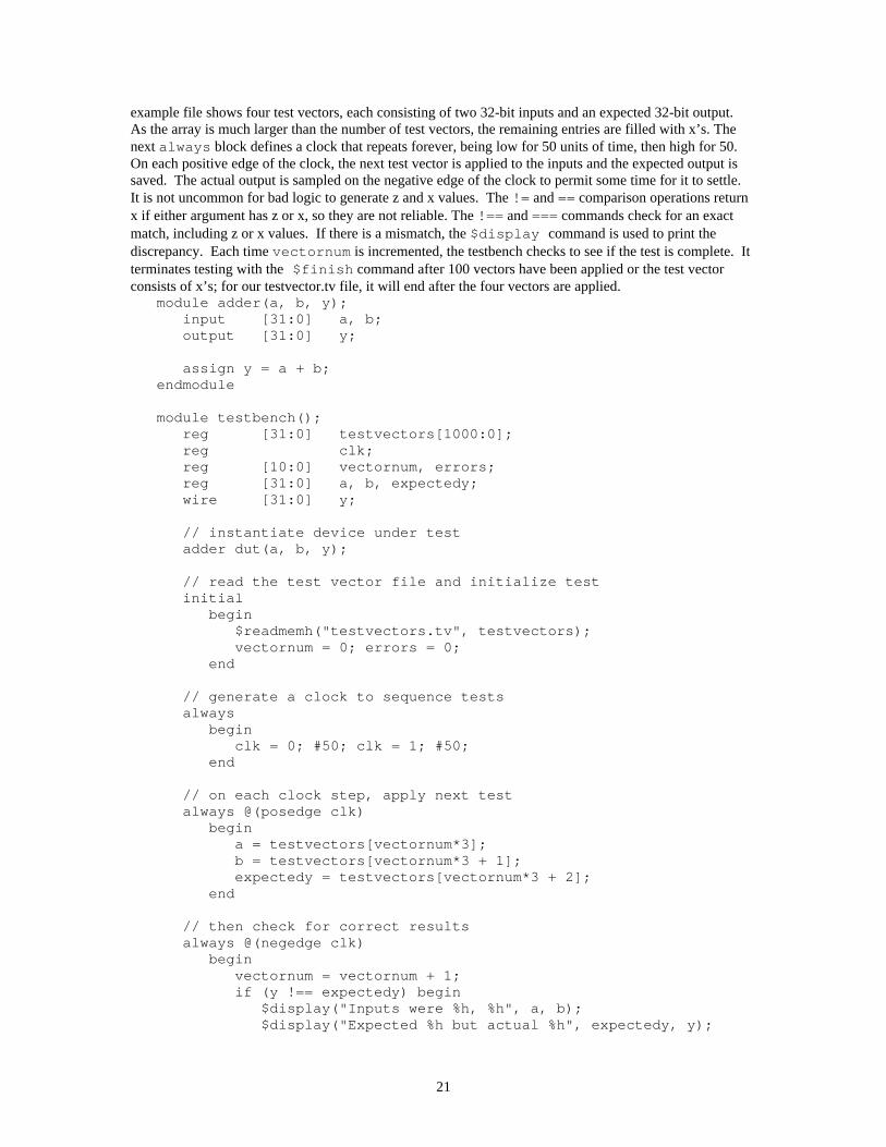
21
example file shows four test vectors, each consisting of two 32-bit inputs and an expected 32-bit output. As the array is much larger than the number of test vectors, the remaining entries are filled with x’s. The next always block defines a clock that repeats forever, being low for 50 units of time, then high for 50. On each positive edge of the clock, the next test vector is applied to the inputs and the expected output is saved. The actual output is sampled on the negative edge of the clock to permit some time for it to settle. It is not uncommon for bad logic to generate z and x values. The != and == comparison operations return x if either argument has z or x, so they are not reliable. The !== and === commands check for an exact match, including z or x values. If there is a mismatch, the $display command is used to print the discrepancy. Each time vectornum is incremented, the testbench checks to see if the test is complete. It terminates testing with the $finish command after 100 vectors have been applied or the test vector consists of x’s; for our testvector.tv file, it will end after the four vectors are applied.
module adder(a, b, y); input [31:0] a, b; output [31:0] y; assign y = a + b; endmodule module testbench(); reg [31:0] testvectors[1000:0]; reg clk; reg [10:0] vectornum, errors; reg [31:0] a, b, expectedy; wire [31:0] y; // instantiate device under test adder dut(a, b, y); // read the test vector file and initialize test initial begin $readmemh("testvectors.tv", testvectors);
vectornum = 0; errors = 0; end
// generate a clock to sequence tests always begin clk = 0; #50; clk = 1; #50; end // on each clock step, apply next test always @(posedge clk) begin a = testvectors[vectornum*3]; b = testvectors[vectornum*3 + 1]; expectedy = testvectors[vectornum*3 + 2]; end // then check for correct results always @(negedge clk) begin vectornum = vectornum + 1; if (y !== expectedy) begin $display("Inputs were %h, %h", a, b); $display("Expected %h but actual %h", expectedy, y);
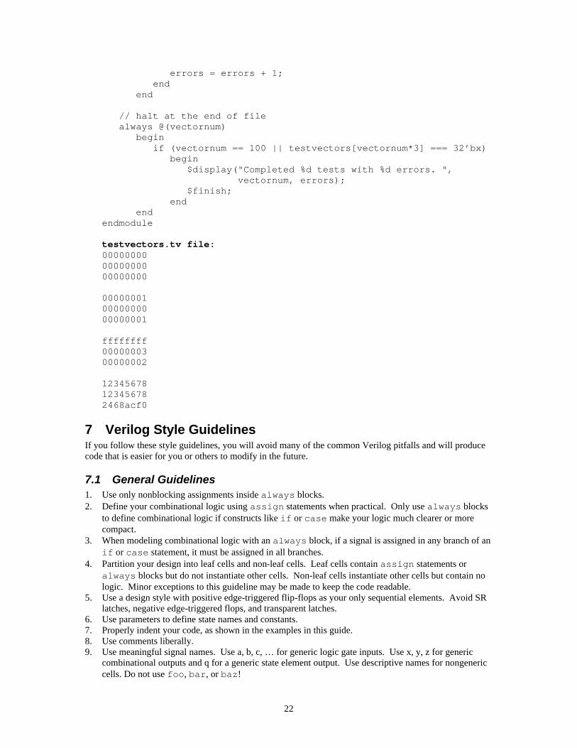
22
errors = errors + 1; end end // halt at the end of file always @(vectornum) begin if (vectornum == 100 || testvectors[vectornum*3] === 32’bx) begin $display("Completed %d tests with %d errors. ", vectornum, errors); $finish; end end endmodule
testvectors.tv file: 00000000 00000000 00000000 00000001 00000000 00000001 ffffffff 00000003 00000002 12345678 12345678 2468acf0
7 Verilog Style Guidelines If you follow these style guidelines, you will avoid many of the common Verilog pitfalls and will produce code that is easier for you or others to modify in the future.
7.1 General Guidelines 1. Use only nonblocking assignments inside always blocks. 2. Define your combinational logic using assign statements when practical. Only use always blocks
to define combinational logic if constructs like if or case make your logic much clearer or more compact.
3. When modeling combinational logic with an always block, if a signal is assigned in any branch of an if or case statement, it must be assigned in all branches.
4. Partition your design into leaf cells and non-leaf cells. Leaf cells contain assign statements or always blocks but do not instantiate other cells. Non-leaf cells instantiate other cells but contain no logic. Minor exceptions to this guideline may be made to keep the code readable.
5. Use a design style with positive edge-triggered flip-flops as your only sequential elements. Avoid SR latches, negative edge-triggered flops, and transparent latches.
6. Use parameters to define state names and constants. 7. Properly indent your code, as shown in the examples in this guide. 8. Use comments liberally. 9. Use meaningful signal names. Use a, b, c, … for generic logic gate inputs. Use x, y, z for generic
combinational outputs and q for a generic state element output. Use descriptive names for nongeneric cells. Do not use foo, bar, or baz!
23
10. Be consistent in your use of capitalization and underscores.
7.2 Xilinx Hints 1. Use only positive edge-triggered flip-flops. Avoid @(negedge clk) and latches. 2. Be certain not to inadvertently imply latches. If you do and are targeting the Spartan family of FPGAs,
which do not have built-in latches, you will get the following warning, which you should fix. The warning will not appear when targeting the 4000XL or SpartanXL families that have latches, but you should still be careful not to inadvertently create logic that implies latches.
Warning: Latch inferred in design ‘…’ read with ‘hdlin_check_no_latch’. (HDL-307)
3. Provide an asynchronous reset to all of your flip-flops with a common signal name. If you do, Xilinx
will automatically tie this reset to the chip’s global reset and reset your flip-flops on power-up. If not, Xilinx will give you the following warnings. Fix the warning by providing a proper reset to all elements.
Warning: No net is connected to the set/reset pin of Cell ‘/”q_reg<0>”/Q_reg’. (FPGA-GSRMAP-16) Warning: No global set/reset (GSR) net could be used in the design because there is not a unique net that sets or resets all the sequential cells. (FPGA-GSRMAP-5)
4. Provide a common clock to all of your flip-flops whenever possible. 5. If you get any “Bus Conflict” messages or X’s in your simulation, be sure to find their cause and fix
the problem.
8 Bad Circuit Examples This section includes examples of a number of bad circuits produced by common Verilog coding errors. Some examples include the results of synthesis using Synopsys’ Design Analyzer and/or the Xilinx Foundation tools.
8.1 Incorrect stimulus list The following circuit was intended to be a transparent latch, but the d input was omitted from the stimulus list. When synthesized with Synopsys or Xilinx, it still produces a transparent latch, but with the warning: Warning: Variable 'd' is being read in routine notquitealatch line 8 in file 'J:/Classes/E155/Fall2000/synopsys/notquitealatch.v', but does not occur in the timing control of the block which begins there. (HDL-180)
module notquitealatch(clk, d, q); input clk; input [3:0] d; output [3:0] q; reg [3:0] q; always @(clk) // left out ‘or d’ if (clk) q <= d; endmodule
Similarly, the b input in the following combinational logic was omitted from the stimulus list of the always block. Synopsis successfully created the intended logic, but gave the warning:
24
Warning: Variable 'b' is being read in routine gates line 7 in file 'J:/Classes/E155/Fall2000/synopsys/gates.v', but does not occur in the timing control of the block which begins there. (HDL-180)
module gates(a, b, y1, y2, y3, y4, y5); input [3:0] a; output [3:0] y1, y2, y3, y4, y5; reg [3:0] y1, y2, y3, y4, y5; always @(a) // missing ‘or b’ begin y1 <= a & b; // AND y2 <= a | b; // OR y3 <= a ^ b; // XOR y4 <= ~(a & b); // NAND y5 <= ~(a | b); // NOR end endmodule
Don’t depend on your synthesizer doing the right thing when an input is omitted. If you see such a warning, correct your code. The next example is supposed to model a multiplexer, but the author incorrectly wrote @(posedge s) rather than @(s). This would result in meaningless logic because s must be high immediately after the positive edge of s. The Xilinx tools give the following error message:
Error: clock variable s is being used as data. (HDL-175)
module badmux(d0, d1, s, y); input [3:0] d0, d1; input s; output [3:0] y; reg [3:0] y; always @(posedge s) if (s) y <= d1; else y <= d0; endmodule
8.2 Missing begin/end block In the following example, two variables are supposed to be assigned in the always block. The begin/end block is missing. Synopsys gives the following error trying to read the design. Xilinx gives the same error. Error: syntax error at or near token '[' (File: J:/Classes/E155/Fall2000/synopsys/flop2.v Line: 10) (VE-0) Error: Can't read 'verilog' file 'J:/Classes/E155/Fall2000/synopsys/flop2.v'. (UID-59)
25
module notquiteatwobitflop(clk, d, q); input clk; input [1:0] d; output [1:0] q; reg [1:0] q; always @(posedge clk) q[1] = d[1]; q[0] = d[0]; endmodule
8.3 Undefined Outputs In the next example of a finite state machine, the user intended out1 to be high when the state is 0 and out2 to be high when the state is 1. However, the code neglects to ever set the outputs low.
module FSMbad(clk, a, out1, out2); input clk; input a; output out1, out2; reg state; reg out1, out2; always @(posedge clk) if (state == 0) begin if (a) state <= 1; end else begin if (~a) state <= 0; end always @(state) // neglect to set out1/out2 to 0 if (state == 0) out1 <= 1; else out2 <= 1; endmodule
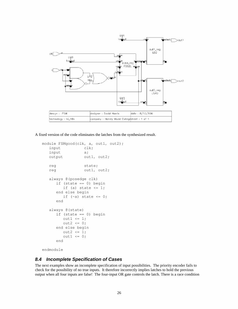
The FSM synthesizes into a circuit with an SR latch and a transparent latch that can set the output high but never reset the output low, as shown below:
26
A fixed version of the code eliminates the latches from the synthesized result.
module FSMgood(clk, a, out1, out2); input clk; input a; output out1, out2; reg state; reg out1, out2; always @(posedge clk) if (state == 0) begin if (a) state <= 1; end else begin if (~a) state <= 0; end always @(state) if (state == 0) begin out1 <= 1; out2 <= 0; end else begin out2 <= 1; out1 <= 0; end endmodule
8.4 Incomplete Specification of Cases The next examples show an incomplete specification of input possibilities. The priority encoder fails to check for the possibility of no true inputs. It therefore incorrectly implies latches to hold the previous output when all four inputs are false! The four-input OR gate controls the latch. There is a race condition
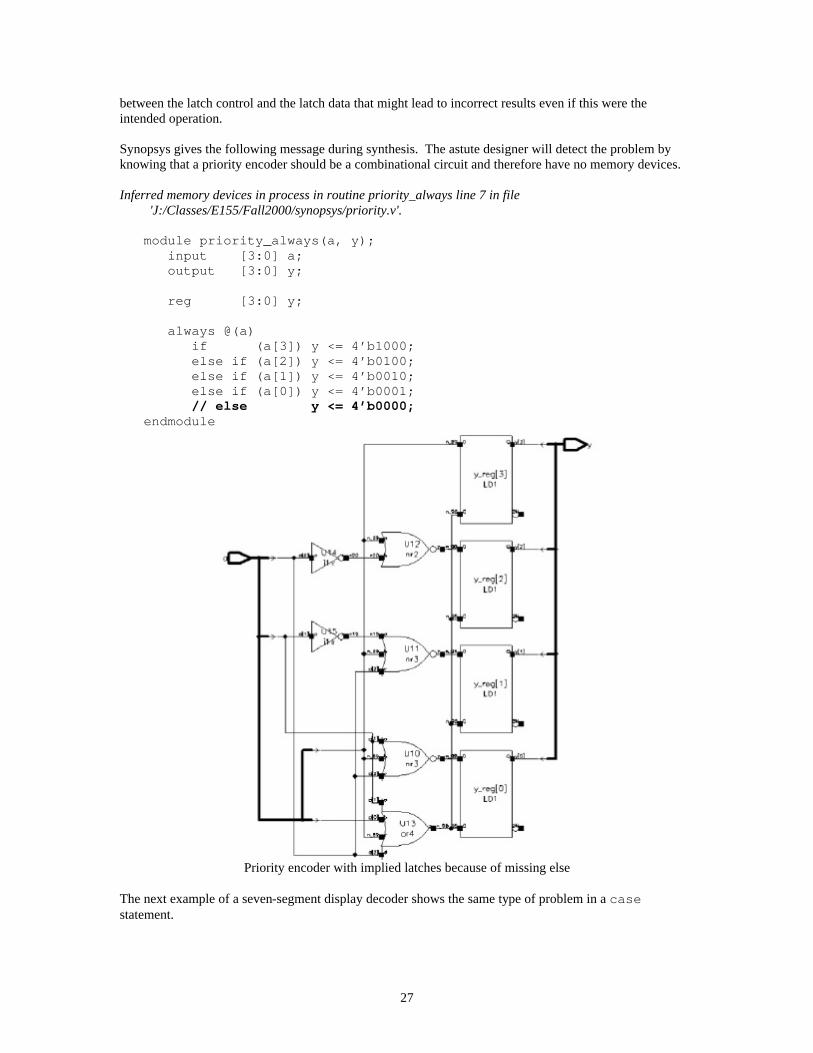
27
between the latch control and the latch data that might lead to incorrect results even if this were the intended operation. Synopsys gives the following message during synthesis. The astute designer will detect the problem by knowing that a priority encoder should be a combinational circuit and therefore have no memory devices. Inferred memory devices in process in routine priority_always line 7 in file 'J:/Classes/E155/Fall2000/synopsys/priority.v'.
module priority_always(a, y); input [3:0] a; output [3:0] y; reg [3:0] y; always @(a) if (a[3]) y <= 4’b1000; else if (a[2]) y <= 4’b0100; else if (a[1]) y <= 4’b0010; else if (a[0]) y <= 4’b0001; // else y <= 4’b0000; endmodule
Priority encoder with implied latches because of missing else
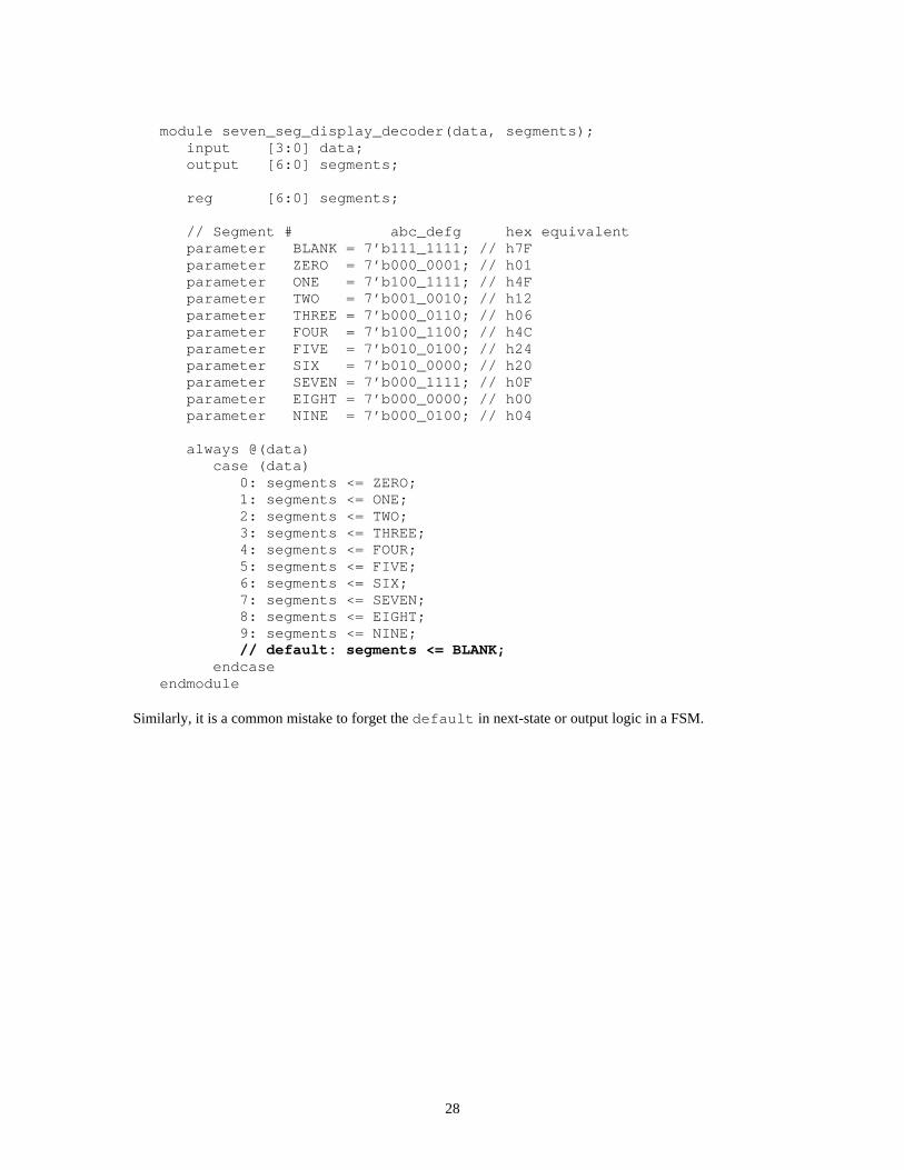
The next example of a seven-segment display decoder shows the same type of problem in a case statement.
28
module seven_seg_display_decoder(data, segments); input [3:0] data; output [6:0] segments; reg [6:0] segments; // Segment # abc_defg hex equivalent parameter BLANK = 7’b111_1111; // h7F parameter ZERO = 7’b000_0001; // h01 parameter ONE = 7’b100_1111; // h4F parameter TWO = 7’b001_0010; // h12 parameter THREE = 7’b000_0110; // h06 parameter FOUR = 7’b100_1100; // h4C parameter FIVE = 7’b010_0100; // h24 parameter SIX = 7’b010_0000; // h20 parameter SEVEN = 7’b000_1111; // h0F parameter EIGHT = 7’b000_0000; // h00 parameter NINE = 7’b000_0100; // h04 always @(data) case (data) 0: segments <= ZERO; 1: segments <= ONE; 2: segments <= TWO; 3: segments <= THREE; 4: segments <= FOUR; 5: segments <= FIVE; 6: segments <= SIX; 7: segments <= SEVEN; 8: segments <= EIGHT; 9: segments <= NINE; // default: segments <= BLANK; endcase endmodule
Similarly, it is a common mistake to forget the default in next-state or output logic in a FSM.

29
module divideby3FSM(clk, reset, out); input clk; input reset; output out; reg [1:0] state; wire [1:0] nextstate; parameter S0 = 2’b00; parameter S1 = 2’b01; parameter S2 = 2’b10; // State Register always @(posedge clk or posedge reset) if (reset) state <= S0; else state <= nextstate; // Next State Logic always @(state) case (state) S0: nextstate <= S1; S1: nextstate <= S2; S2: nextstate <= S0; //default: nextstate <= S0; endcase // Output Logic assign out = (state == S2); endmodule
8.5 Shorted Outputs Bad code may sometimes lead to shorted outputs of gates. For example, the tristate drivers in the following multiplexer should have mutually exclusive enable signals, but instead are both active simultaneously and produce a conflict when d0 and d1 are not equal. Synthesis may not report any errors. However, during simulation, you will observe X’s rather than 0’s or 1’s when the bus is simultaneously being driven high and low. You may also get a “Bus Conflict” warning message.
module mux2(d0, d1, s, y); input [3:0] d0, d1; input s; output [3:0] y; tristate t0(d0, s, y); // should have been ~s tristate t1(d1, s, y); endmodule
Another cause of shorted outputs is when a reg is assigned in two different always blocks. For example, the following code trys to model a flip-flop with asynchronous reset and asynchronous set. The first

30
always block models the reset and ordinary operation. The second always block attempts to incorporate the asynchronous set. Synthesis infers a separate piece of hardware for each always block, with a shorted output. Xilinx reports the following error:
Error: the net '/ver1/q' has more than one driver (FPGA-CHECK-5) The module also produces a warning because the second always block implies a latch.
module floprs(clk, reset, set, d, q); input clk; input reset; input set; // force q true input d; output q; reg q; always @(posedge clk or posedge reset) if (reset) q <= 0; else q <= d; always @(set) if (set) q <= 1; endmodule