an fpga spectrum sensing accelerator for cognitive...
TRANSCRIPT

GE100111U-100A.ai
An FPGA Spectrum SensingAccelerator for Cognitive Radio
George EichingerMiriam Leeser
Kaushik Chowdhury
NEWSDR’11
01 October 2011
This work is sponsored by the Department of the Air Force under Air Force Contract FA8721-05-C-0002. The opinions, interpretations, conclusions, and recommendations are those of the authors and are not necessarily endorsed by the United States Government

GE092111U-101ANORTHEASTERN
Cognitive Radio Overview
U N I V E R S I T Y
• Cognitive radios allow you to operate in unused portions of spectrum
Spectrum Holes
Time
Freq
uenc
y
GE092111U-602AA.ai
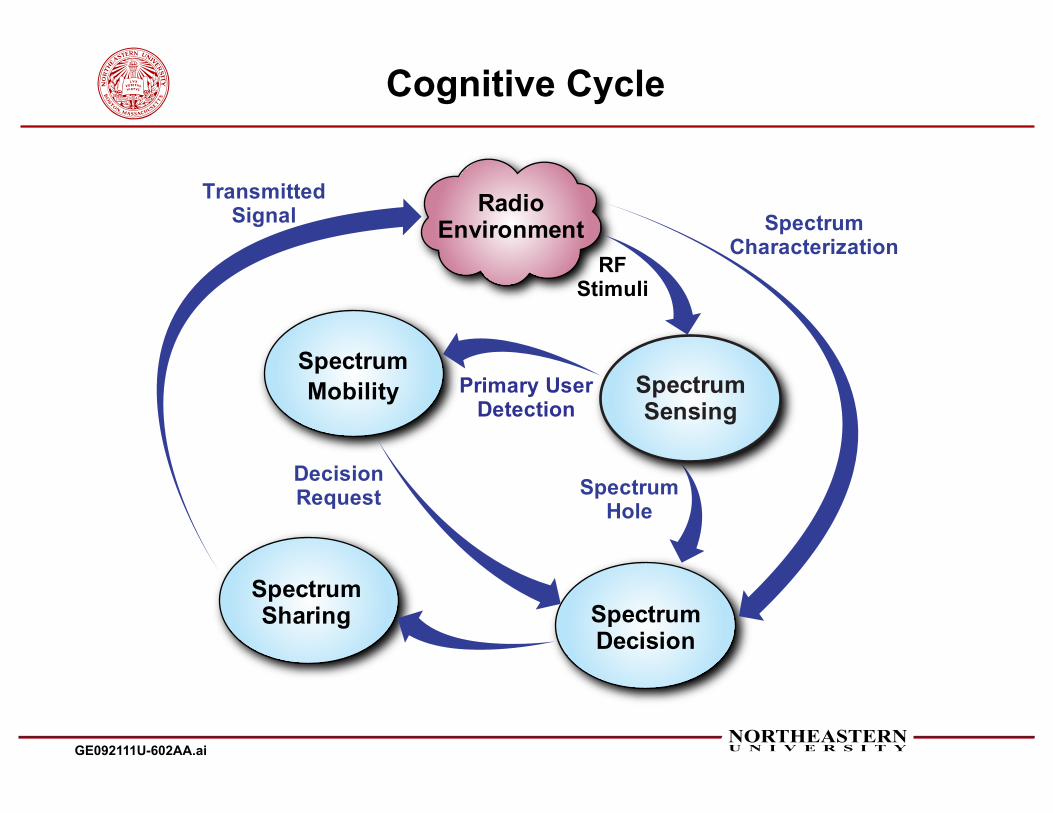
Cognitive Cycle
NORTHEASTERNU N I V E R S I T Y
SpectrumCharacterization
RFStimuli
SpectrumHole
Primary UserDetection
DecisionRequest
TransmittedSignal
Spectrum Mobility
RadioEnvironment
SpectrumDecision
SpectrumSharing
SpectrumSensing

GE092111U-602AA.ai
Cognitive Cycle
NORTHEASTERNU N I V E R S I T Y
SpectrumCharacterization
RFStimuli
SpectrumHole
Primary UserDetection
DecisionRequest
TransmittedSignal
Spectrum Mobility
RadioEnvironment
SpectrumDecision
SpectrumSharing
SpectrumSensing
SpectrumSensing
Focus ofThis Talk

GE092111U-102ANORTHEASTERN
Outline
U N I V E R S I T Y
• Cognitive Radio overview
• Project motivation and goals
• Hardware platform
• Spectrum sensing algorithm
• Results of implementation
• Summary
GE092111U-103ANORTHEASTERN
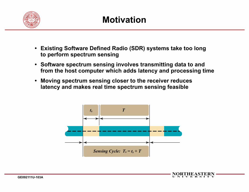
Motivation
U N I V E R S I T Y
• Existing Software Defined Radio (SDR) systems take too long to perform spectrum sensing
• Software spectrum sensing involves transmitting data to and from the host computer which adds latency and processing time
• Moving spectrum sensing closer to the receiver reduces latency and makes real time spectrum sensing feasible
ts T
Sensing Cycle: Ts = ts + T
GE092111U-104ANORTHEASTERN
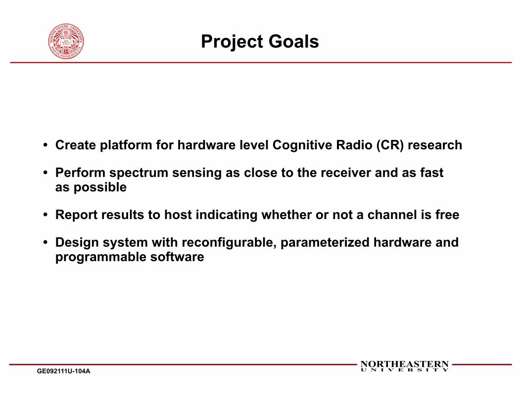
Project Goals
U N I V E R S I T Y
• Create platform for hardware level Cognitive Radio (CR) research
• Perform spectrum sensing as close to the receiver and as fast as possible
• Report results to host indicating whether or not a channel is free
• Design system with reconfigurable, parameterized hardware and programmable software
GE092111U-102ANORTHEASTERN
Outline
U N I V E R S I T Y
• Cognitive Radio overview
• Project motivation and goals
• Hardware platform – Cognitive Radio Universal Software Hardware (CRUSH)
• Spectrum sensing algorithm
• Results of implementation
• Summary

GE092111U-105A.aiNORTHEASTERN
Introducing CRUSH
U N I V E R S I T Y
Cognitive Radio Universal Software Hardware (CRUSH)
• Standard software defined radio and FPGA development board• Custom interface board to connect the two boards
Xilinx ML605FPGA Board
CustomInterface
Board
Ettus USRPN210

GE092111U-106ANORTHEASTERN
Ettus Research USRP N210
U N I V E R S I T Y
• Agile front end• Low cost• Xilinx Spartan 3A DSP FPGA for RX/TX• Minor changes for CRUSH
GE100111U-107ANORTHEASTERN
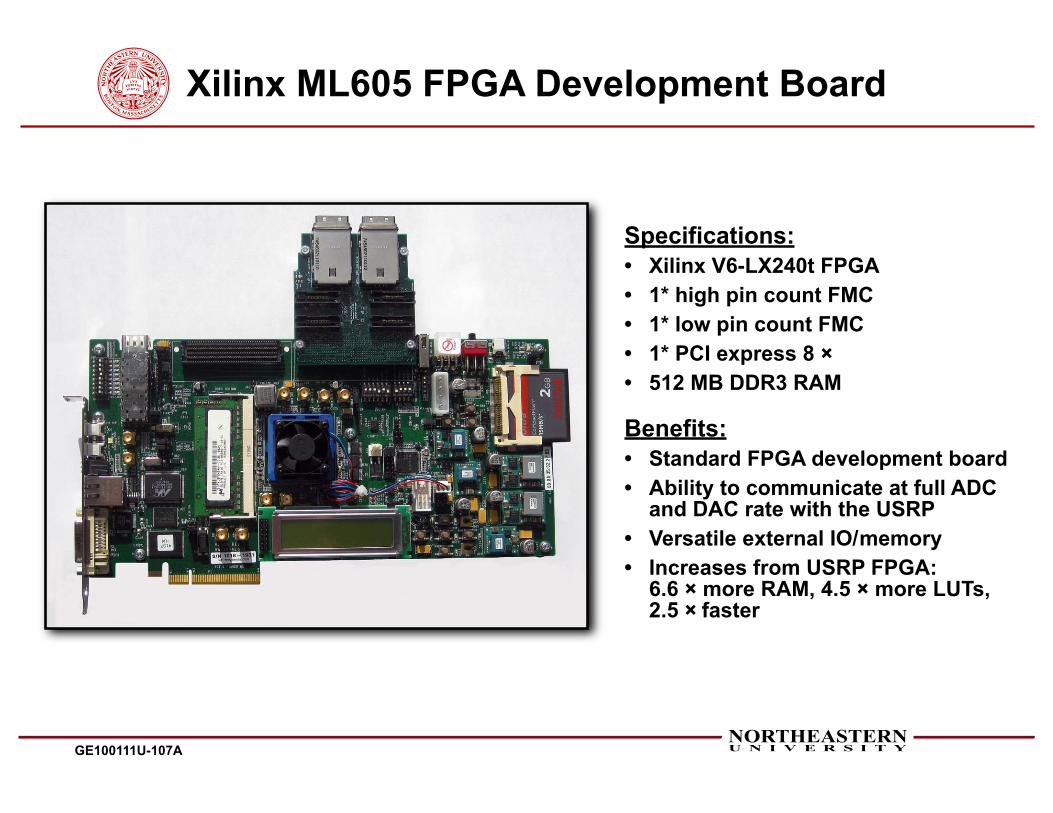
Xilinx ML605 FPGA Development Board
U N I V E R S I T Y
Specifications:• Xilinx V6-LX240t FPGA• 1* high pin count FMC• 1* low pin count FMC• 1* PCI express 8 ו 512 MB DDR3 RAM
Benefits:• Standard FPGA development board• Ability to communicate at full ADC and DAC rate with the USRP• Versatile external IO/memory• Increases from USRP FPGA: 6.6 × more RAM, 4.5 × more LUTs, 2.5 × faster

GE100111U-108ANORTHEASTERN
Custom Interface Board
U N I V E R S I T Y
• 2 Mictor connectors – Allows for ML605 to communicate with two USRPs via the 34 pin parallel debug port
• 2 miniSAS posts – Transmit serial data with up to two USRPs via MIMO port
• 2 spare Mictor connectors – Spare FPGA IO
• FMC HPC/LPC interface – Fully compatible with the ML605 – Can be used with and LPC interface like the SP605 with just one USRP
• Only custom part of CRUSH
• Allows full 100 MSPS IQ bidirectional datalink up to 800 MB/s
GE092111U-102ANORTHEASTERN
Outline
U N I V E R S I T Y
• Cognitive Radio overview
• Project motivation and goals
• Hardware platform
• Spectrum sensing algorithm
• Results of implementation
• Summary
GE092111U-109ANORTHEASTERN
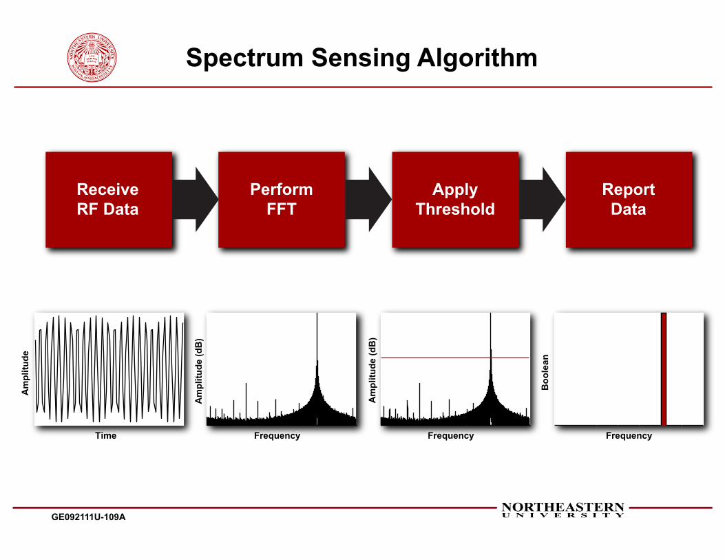
Spectrum Sensing Algorithm
U N I V E R S I T Y
Time
Am
plitu
de
Frequency
Am
plitu
de (d
B)
Frequency
Am
plitu
de (d
B)
ReceiveRF Data
PerformFFT
ApplyThreshold
ReportData
Frequency
Boo
lean

GE092111U-110AANORTHEASTERNU N I V E R S I T Y
Digital DownConverter
(DDC)
ADC
Digital UpConverter
(DUC)
Radio Receiver FFT
USRPRF
IF
IFDAC Data
Frequency SelectionHost
Control Logic
TransmitterR
F Host
• All processing occurs on the host• No real-time guarantee
System Diagram – Spectrum Sensing without CRUSH

GE092111U-110AANORTHEASTERNU N I V E R S I T Y
Digital DownConverter
(DDC)
ADC
Digital UpConverter
(DUC)
Radio Receiver FFT
USRPRF
IF
IFDAC Data
Frequency SelectionHost
Control Logic
TransmitterR
F Host
FIFO Samples Freq BinsFFT Freq BinsThresholdDetector
FrequencyStatus
Accumulator
ML605Control Logic
Receiver
Host
ML605
DAC Data
Frequency SelectionHost
Control Logic
Transmitter
AD
C D
ata
Host
System Diagram – Spectrum Sensing with CRUSH
GE092111U-111ANORTHEASTERN
Advantages of CRUSH
U N I V E R S I T Y
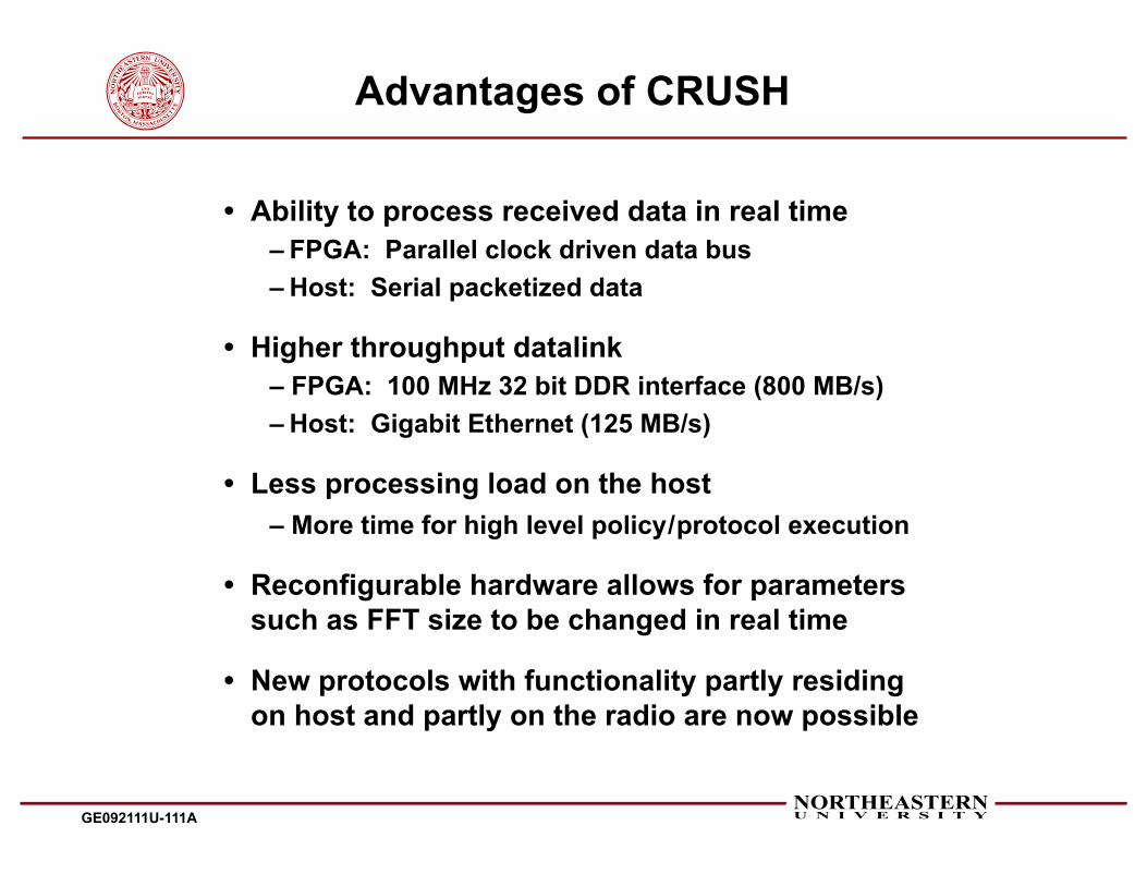
• Ability to process received data in real time – FPGA: Parallel clock driven data bus – Host: Serial packetized data
• Higher throughput datalink – FPGA: 100 MHz 32 bit DDR interface (800 MB/s) – Host: Gigabit Ethernet (125 MB/s)
• Less processing load on the host – More time for high level policy/protocol execution
• Reconfigurable hardware allows for parameters such as FFT size to be changed in real time
• New protocols with functionality partly residing on host and partly on the radio are now possible

GE092111U-102ANORTHEASTERN
Outline
U N I V E R S I T Y
• Cognitive Radio overview
• Project motivation and goals
• Hardware platform
• Spectrum sensing algorithm
• Results of implementation
• Summary

GE092111U-112ANORTHEASTERN
Test Setup – Functional Verification
U N I V E R S I T Y
Signal Generators
USRP ML605
Host

GE092111U-113ANORTHEASTERN
Results – Functionality Verification
U N I V E R S I T Y
• Lab measurement with one tone at 31 MHzand a center frequency of 25 MHz
10 20 30 40 50-80
-70
-60
-50
-40
-30
-20
-10
0X: 3.086e+007Y: 0
256-point FFT – Processed by FPGA
Frequency in MHz
Am
plitu
de (d
Bc)
15 20 25 30 35-80
-70
-60
-50
-40
-30
-20
-10
0 X: 3.1e+007Y: 0
FFT of USRP data Processed in Matlab
Frequency in MHz
Am
plitu
de (d
Bc)

GE092111U-114ANORTHEASTERN
Test Setup – Runtime Analysis
U N I V E R S I T Y
Digital DownConverter
(DDC)
ADC
Digital UpConverter
(DUC)
Radio Receiver FFT
USRPRF
IF
IFDAC Data
Frequency SelectionHost
Control Logic
TransmitterR
F Host
FIFOSamples FFT Timers
ML605Control Logic
USRPControl Logic
ML605
AD
C D
ata
Two
Way
Sta
tus
Two Way Status
GE092111U-115AANORTHEASTERN
Test Setup – Runtime Analysis
U N I V E R S I T Y
Digital DownConverter
(DDC)
ADC
Digital UpConverter
(DUC)
Radio Receiver FFT
USRPRF
IF
IF
DAC Data
Frequency SelectionHost
Control Logic
Transmitter
RF Host
FIFOSamples FFT Timers
ML605Control Logic
USRPControl Logic
ML605
AD
C D
ata
Two
Way
Sta
tus
Two Way Status
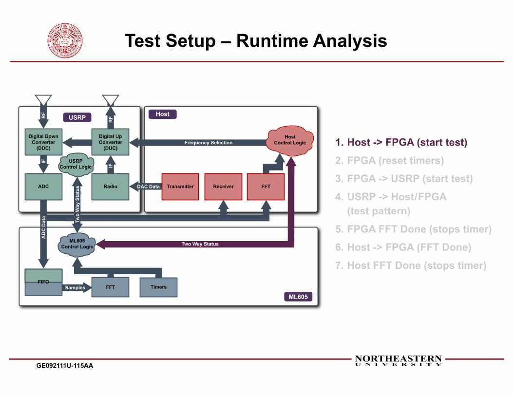
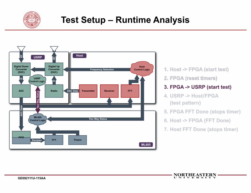
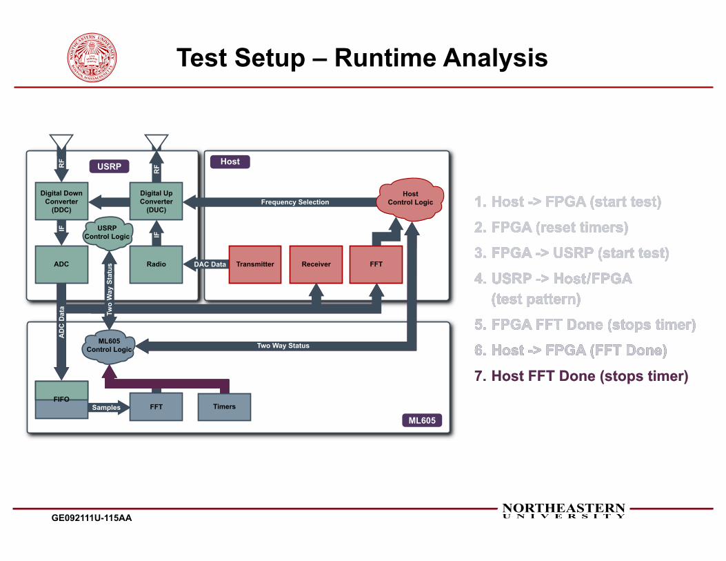
1. Host -> FPGA (start test)
2. FPGA (reset timers)
3. FPGA -> USRP (start test)
4. USRP -> Host/FPGA (test pattern)
5. FPGA FFT Done (stops timer)
6. Host -> FPGA (FFT Done)
7. Host FFT Done (stops timer)

GE092111U-115AANORTHEASTERN
Test Setup – Runtime Analysis
U N I V E R S I T Y
Digital DownConverter
(DDC)
ADC
Digital UpConverter
(DUC)
Radio Receiver FFT
USRPRF
IF
IF
DAC Data
Frequency SelectionHost
Control Logic
Transmitter
RF Host
FIFOSamples FFT Timers
ML605Control Logic
USRPControl Logic
ML605
AD
C D
ata
Two
Way
Sta
tus
Two Way Status
1. Host -> FPGA (start test)
2. FPGA (reset timers)
3. FPGA -> USRP (start test)
4. USRP -> Host/FPGA (test pattern)
5. FPGA FFT Done (stops timer)
6. Host -> FPGA (FFT Done)
7. Host FFT Done (stops timer)
1. Host -> FPGA (start test)
2. FPGA (reset timers)
3. FPGA -> USRP (start test)
4. USRP -> Host/FPGA (test pattern)
5. FPGA FFT Done (stops timer)
6. Host -> FPGA (FFT Done)
7. Host FFT Done (stops timer)
Two Way Status
1. Host -> FPGA (start test)
2. FPGA (reset timers)
3. FPGA -> USRP (start test)
4. USRP -> Host/FPGA (test pattern)
5. FPGA FFT Done (stops timer)
6. Host -> FPGA (FFT Done)
7. Host FFT Done (stops timer)
Two
Way
Sta
tus
1. Host -> FPGA (start test)
2. FPGA (reset timers)
3. FPGA -> USRP (start test)
4. USRP -> Host/FPGA (test pattern)
5. FPGA FFT Done (stops timer)
6. Host -> FPGA (FFT Done)
7. Host FFT Done (stops timer)
AD
C D
ata
Two
Way
Sta
tus
1. Host -> FPGA (start test)
2. FPGA (reset timers)
3. FPGA -> USRP (start test)
4. USRP -> Host/FPGA (test pattern)
5. FPGA FFT Done (stops timer)
6. Host -> FPGA (FFT Done)
7. Host FFT Done (stops timer)
AD
C D
ata
Two
Way
Sta
tus
1. Host -> FPGA (start test)
2. FPGA (reset timers)
3. FPGA -> USRP (start test)
4. USRP -> Host/FPGA (test pattern)
5. FPGA FFT Done (stops timer)
6. Host -> FPGA (FFT Done)
7. Host FFT Done (stops timer)
Two Way Status
1. Host -> FPGA (start test)
2. FPGA (reset timers)
3. FPGA -> USRP (start test)
4. USRP -> Host/FPGA (test pattern)
5. FPGA FFT Done (stops timer)
6. Host -> FPGA (FFT Done)
7. Host FFT Done (stops timer)
Two Way Status

GE092111U-116ANORTHEASTERN
256-point FPGA FFT Timing Analysis
U N I V E R S I T Y
270 ns2560 ns
9410 ns
ActionStart Test 0 0 0Data enters FPGA Clock Domain 27 0.27 0.27FFT Starts 27 0.27 0All Data inside FPGA 256 2.56 2.83FFT Complete 941 9.41 6.58Total 941 9.41 9.41
Clocks Time (µs) Incremental (µs)

GE092111U-117AANORTHEASTERN
Results – Runtime Analysis
U N I V E R S I T Y
FFT Size
8 1.17 907.72 77416 1.91 915.89 47932 2.38 920.07 38664 3.56 925.47 259128256512102420484096
5.479.5617.2332.8463.55125.24
916.541198.191003.83955.30995.261071.79
1255829158
167
FPGAAverage (µs)
HostAverage (µs) Speed-up (×)
• Speed-up between 8 and 774 ו FPGA timing scales log linear with FFT size• Host timing driven by packet transmit time and internal buffering
GE092111U-118ANORTHEASTERN
Conclusion
U N I V E R S I T Y
• Created CRUSH platform – Combined powerful FPGA with versatile RF front end
– Produced custom interface board to allow high speed data transfer
– Moved processing closer to receiver
• Implemented spectrum sensing on CRUSH – Achieved more than 100 × performance for FFT sizes of interest
– Reduced load on host computer
– Fully configurable
GE092111U-119ANORTHEASTERN
Future Work
U N I V E R S I T Y
• Integrate the spectrum sensing module into research on Cognitve Radio at Northeastern University
• Explore other methods of performing hardware accelerated spectrum sensing such as wavelet analysis
• Utilize the CRUSH platform to migrate additional software radio functions into reconfigurable hardware
• Perform non-radio research with the CRUSH platform utilizing its RF front end and FPGA back end

GE092111U-120ANORTHEASTERNU N I V E R S I T Y
Questions?Questions?
Miriam [email protected]
http://www.coe.neu.edu/Research/rcl/index.php
George [email protected]
Kaushik [email protected]
http://indigo.ece.neu.edu/~krc/#research

GE100111U-121ANORTHEASTERN
Issues Using the USRP N210 FPGA
U N I V E R S I T Y
• USRP N210 has a Xilinx Spartan 3A-DSP3400A
• Timing closure is an issue – 100 MHz clock speed makes timing closure more difficult
• Long build time and complex existing firmware
• Spartan 3A DSP line is two generations behind the latest Xilinx products
• USRP N210 FPGA is an improvement over the FPGA used in the USRP 2 but still not enough – 64 k Xilinx FFT takes 367 RAM36 blocks, more than the entire USRP N210 FPGA
• No ability for partial reconfiguration applications
• Limited external IO and memory