an adaptive 3d machine vision system for electronic
TRANSCRIPT

An adaptive 3D machine vision system for electronic components inspection
Department of IE&MYuan-Ze University
Hsu-Nan Yen Du-Ming Tsai
Contents
Introduction
Method
System description
Experimental results
Conclusion

Introduction -Status in electronic industry
light, thin, small and multifunctional electronic products
minify electronic componentshigh-density packaging
3D measurementto ensure reliability
-

Introduction -Some methods for 3D measurement
Laser scanning techniques
X-ray detection methods
Microscope inspection with focus-based methods
Projected fringes with phase shifting techniques

Introduction -Some methods for 3D measurement
Laser scanning techniquesslow with a point-by-point or line-by-line scan
measuring accuracy is affected by the beam spot reflection and stray light.
X-ray detection methods
Microscope inspection with focus-based methods
Projected fringes with phase shifting techniques

Introduction -Some methods for 3D measurement
Laser scanning techniques
X-ray detection methodsrequire expensive equipment
suffer from long measuring time
Microscope inspection with focus-based methods
Projected fringes with phase shifting techniques

Introduction -Some methods for 3D measurement
Laser scanning techniques
X-ray detection methods
Microscope inspection with focus-based methodsinherently small effective area of detection
Projected fringes with phase shifting techniques

Introduction -Some methods for 3D measurement
Laser scanning techniques
X-ray detection methods
Microscope inspection with focus-based methods
Projected fringes with phase shifting techniquesfull-field 3D measurement fast inspection
high accuracy

Method -Relationship between surface height and phase
General optical geometry of projected fringes method.
• The surface height is determined by
the difference of and .
)],(),([ yxyxk or φφ −⋅=
),( yxrφ is the phase function on the reference plane;
),( yxoφ is the phase function in the presence of object.
),( yxrφ
),( yxh
),( yxoφ
CCDGrating
P0
D
C B AReference plane
θdθp
h(x,y)Object
z
O
)tantan
1(
tan),(
p
d
dACyxh
θθ
θ
+=
A projected sinusoidal fringe image can be expressed as),(cos),(),(),( yxyxIyxIyxI mb φ+=
where k is a constant for a given system setup;

Method -Extracting phase from intensity images
),(cos),(),(]0),(cos[),(),(),(1 yxyxIyxIyxyxIyxIyxI mbmb φφ +=++=
),(sin),(),(]2
),(cos[),(),(),(2 yxyxIyxIyxyxIyxIyxI mbmb φπφ −=++=
),(cos),(),(]),(cos[),(),(),(3 yxyxIyxIyxyxIyxIyxI mbmb φπφ −=++=
),(sin),(),(]2
3),(cos[),(),(),(4 yxyxIyxIyxyxIyxIyxI mbmb φπφ +=++=
−−
= −
31
241tan),(IIIIyxφ
Chooseπ/2 as phase shifting increment and adopt four-step phase shifting method.
[ ])(),(cos),(),(),( tyxyxIyxIyxI mbn δφ ++=
and can be obtained by using phase shifting technique.
where )(tδ is the introduced phase shift.
),( yxrφ ),( yxoφand
),( yxrφ ),( yxoφ
The fundamental formula of phase shifting technique is

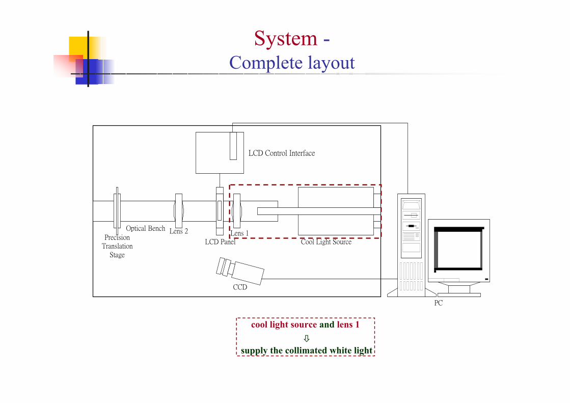
System -Complete layout
PC
LCD Control Interface
PrecisionTranslation
Stage
Lens 2 Lens 1LCD Panel
CCD
Cool Light Source
Optical Bench
System -Complete layout
PC
LCD Control Interface
PrecisionTranslation
Stage
Lens 2 Lens 1LCD Panel
CCD
Cool Light Source
Optical Bench
cool light source and lens 1
supply the collimated white light

System -Complete layout
PC
LCD Control Interface
PrecisionTranslation
Stage
Lens 2 Lens 1LCD Panel
CCD
Cool Light Source
Optical Bench
LCD panel
generate transparent sinusoidal gratingshift grating with accurate phase increment

System -Complete layout
PC
LCD Control Interface
PrecisionTranslation
Stage
Lens 2 Lens 1LCD Panel
CCD
Cool Light Source
Optical Bench
lens 2
focus the image of sinusoidal grating

System -Complete layout
PC
LCD Control Interface
PrecisionTranslation
Stage
Lens 2 Lens 1LCD Panel
CCD
Cool Light Source
Optical Bench
precision translation stage
place the object under inspection

System -Complete layout
PC
LCD Control Interface
PrecisionTranslation
Stage
Lens 2 Lens 1LCD Panel
CCD
Cool Light Source
Optical Bench
CCD camera
capture the projected fringe patterns

System -Digital phase shifting
PC
LCD Control Interface
PrecisionTranslation
Stage
Lens 2 Lens 1LCD Panel
CCD
Cool Light Source
Optical Bench
phase shifting is 0
I1(x,y)

System -Digital phase shifting
PC
LCD Control Interface
PrecisionTranslation
Stage
Lens 2 Lens 1LCD Panel
CCD
Cool Light Source
Optical Bench
phase shifting is π/2
I2(x,y)
System -Digital phase shifting
PC
LCD Control Interface
PrecisionTranslation
Stage
Lens 2 Lens 1LCD Panel
CCD
Cool Light Source
Optical Bench
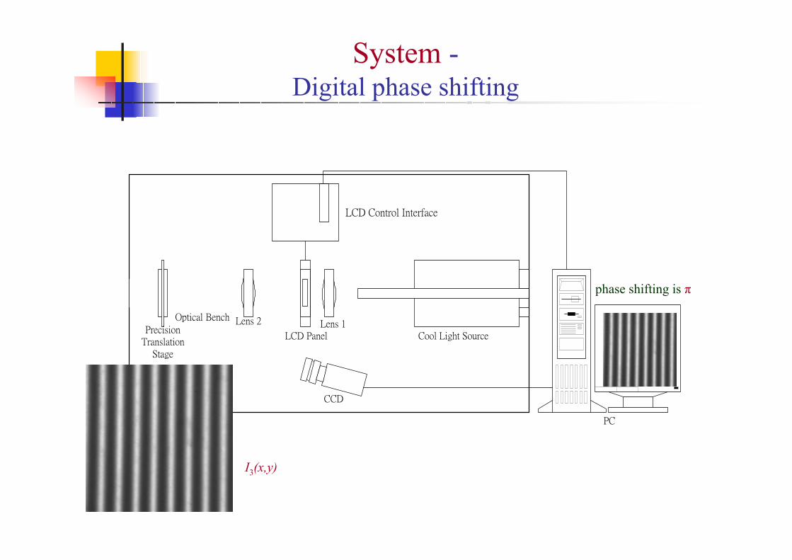
phase shifting is π
I3(x,y)

System -Digital phase shifting
PC
LCD Control Interface
PrecisionTranslation
Stage
Lens 2 Lens 1LCD Panel
CCD
Cool Light Source
Optical Bench
phase shifting is 3 π /2
I4(x,y)

different fringe periods
different phase-variation directions
different grating patterns
easily changed fringe periods,phase-variation directionsand grating patterns
accommodate the topography and reflectanceof various electronic components on PCBs
avoid phase ambiguityreduce overexposure areaincreasing measuring speed
System -Adaptive projection

Experiment -A 1mm gauge block
(a) The 1mm gauge block. (b) The deformed sinusoidal fringes image
of the 1mm gauge block.
(c) The 3D surface profile of the 1mm gauge block.
mean step height is 1.03 mmstandard deviation is 0.04 mm
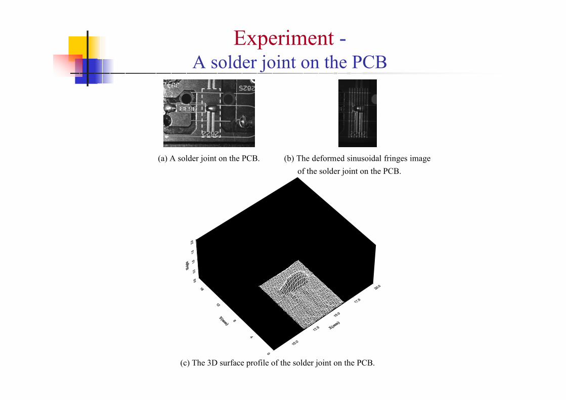
Experiment -A solder joint on the PCB
(a) A solder joint on the PCB. (b) The deformed sinusoidal fringes image
of the solder joint on the PCB.
(c) The 3D surface profile of the solder joint on the PCB.

Experiment -A sample BGA-joint
(a) The sample BGA-joint. (b) The deformed sinusoidal fringes
image of sample BGA-joint.
(c) The 3D surface profile of the sample BGA-joint.
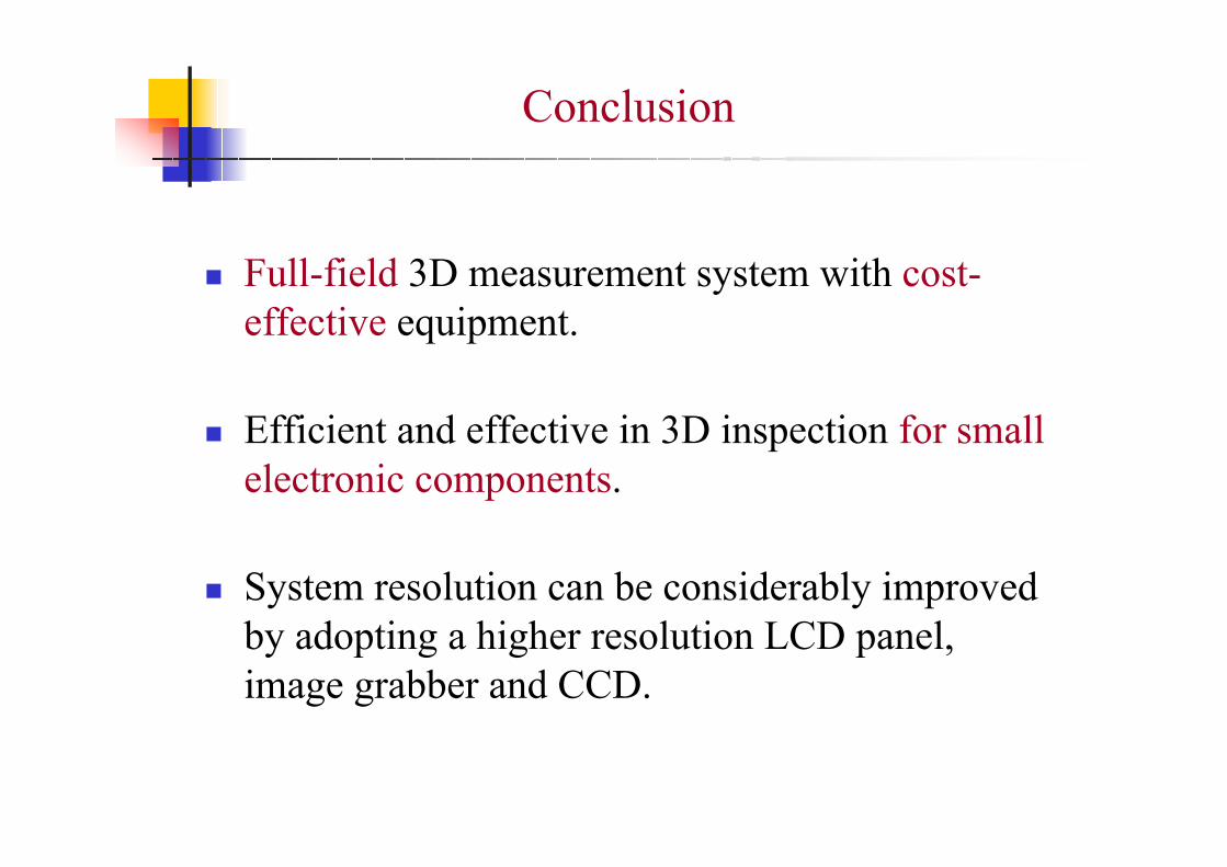
Full-field 3D measurement system with cost-effective equipment.
Efficient and effective in 3D inspection for small electronic components.
System resolution can be considerably improved by adopting a higher resolution LCD panel, image grabber and CCD.
Conclusion