amplifier frequency response(part 1)
TRANSCRIPT

Engr.Tehseen Ahsan
Lecturer, Electrical Engineering Department
EE-307 Electronic Systems Design
HITEC University Taxila Cantt, Pakistan
Amplifier Frequency Response
(Part 1)

10.1 Introduction Previously we neglected the effects of input frequency on an
amplifier’s operation due to capacitive elements in the circuit
in order to focus on other concepts (in EE-205)
The coupling and bypass capacitors were considered to be
ideal shorts and the internal transistor capacitances were
considered to be ideal opens. This treatment is valid when the
frequency is in an amplifier’s midrange.
Since capacitive reactance is inversely proportional to the
input frequency. When the frequency is low enough, the
coupling and bypass capacitors can no longer be considered
as shorts because their reactances are large enough to have a
significant effect.
2

10.1 Introduction continue… Also, when the frequency is high enough, the internal
transistor capacitances can no longer be considered as opens
because their reactances become small enough to have a
significant effect on amplifier operation.
Frequency response of an amplifier is the change in gain
or phase shift over a specified range of input signal
frequencies.
3

Effect of Coupling Capacitors Since capacitive reactance is inversely proportional to frequency. At
lower frequencies ( Audio Frequencies below 10 Hz)- capacitively
coupled amplifiers such as those in figure 10-1 have less voltage
gain than they have at higher frequencies. The reason is that at lower
frequencies more signal is dropped across C1 and C3 because their
reactances are higher. This higher signal voltage drop at lower
frequencies reduces the voltage gain. Also a phase shift is introduced
by the coupling capacitors because C1 forms a lead circuit with Rinof the amplifier and C3 forms a lead circuit with RL in parallel RCwith or RD
Recall an RC circuit ( Output voltage across R leads the input
voltage in phase)
4

Effect of Coupling Capacitors continue..
5

Effect of Bypass Capacitors At low frequencies, the reactance of the bypass capacitor C2 in
figure 10-1, becomes significant and the emitter ( or FET source
terminal) is no longer at ac ground. The capacitive reactance XC2 in
parallel with RE (or RS ) creates an impedance that reduces the gain.
For example when the frequency is sufficiently high, XC = OΩ and
the voltage gain of the CE amplifier is Av = RC/r'e. At Lower
frequencies, XC >> OΩ and the voltage gain is Av= RC/(r'e+ Ze)
6

Effect of Internal Transistor Capacitors At high frequencies the coupling and bypass capacitors become
effective ac shorts and do not affect an amplifier’s response. Internal
transistor capacitances, however do come into play, reducing an
amplifier’s gain and introducing phase shift as the signal frequency
increases.
In figure 10-3 , in the case of BJT, Cbe is the base-emitter junction
capacitance and Cbc is the base-collector junction capacitance
7

Effect of Internal Transistor Capacitors continue…
At lower frequencies, the internal capacitances have a very high
reactance therefore they look like opens and have no effect on the
transistor’s performance.
As the frequency goes up, the internal capacitive reactances go
down and at some point they begin to have a significant effect on
the transistor’s gain.
When the reactance of Cbe becomes small enough, a significant
amount of voltage drop is lost due to voltage divider effect of the
signal source resistance and the reactance Cbe as illustrated in figure
10-4(a)
When the reactance of Cbc becomes small enough, a significant
amount of voltage is fed back out of phase with input (-ve
feedback), thus effectively reducing the voltage gain as shown in
figure 10-4(b)8

Effect of Internal Transistor Capacitors continue…
9
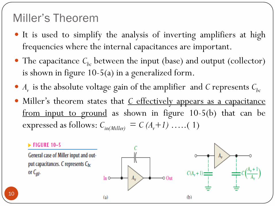
Miller’s Theorem
It is used to simplify the analysis of inverting amplifiers at high
frequencies where the internal capacitances are important.
The capacitance Cbc between the input (base) and output (collector)
is shown in figure 10-5(a) in a generalized form.
Av is the absolute voltage gain of the amplifier and C represents Cbc
Miller’s theorem states that C effectively appears as a capacitance
from input to ground as shown in figure 10-5(b) that can be
expressed as follows: Cin(Miller) = C (Av+1)…..( 1)
10

Miller’s Theorem continue…
Equation 1 shows that Cbc has a much greater impact on input
capacitance than its actual value. If Cbc = 6 pF and amplifier gain is
50 then Cin(Miller) = 306 pF.
Figure 10.6 shows how this effective input capacitance appears in
the actual ac equivalent circuit in parallel with Cbe
11

Miller’s Theorem continue…
Miller’s theorem also states that C effectively appears as a
capacitance from output to ground as shown in Figure 10.5(b), that
can be expressed as follows: Cout(Miller) = C (Av+1/Av)….(2)
Equation 2 indicates that if the voltage gain is 10 or greater
Cout(Miller)=C=Cbc because (Av+1/Av) is approximately equal to 1
12

10.2 The Decibel
Decibels are a form of gain measurement and are commonly used
to express amplifier response.
The decibel is a logarithmic measurement of the ratio of one power
to another or one voltage to another.
Power gain is expressed in decibels (dB) as Ap(dB) = 10 log Ap where
Ap is the actual power gain, Pout/Pin
Voltage gain is expressed in decibels (dB) as Av(dB) = 20 log Av
If Av is greater than 1, the dB gain is positive and if Av is less than 1,
the dB gain is negative and is usually called attenuation.
13
O dB Reference
It is often convenient in amplifiers to assign a certain value of gain
as the O dB reference.
This does not mean that actual voltage gain is 1 ( 0 dB); it means
that the reference gain, no matter what its actual value , is used as a
reference with which to compare other values of gain and is there
assigned a 0 dB value.
Many amplifiers exhibit a maximum gain over a certain range of
frequencies and a reduced gain at frequencies below and above this
range.
The maximum gain occurs for the range of frequencies between the
upper and lower critical frequencies and is called midrange gain,
which is assigned a 0 dB value.
14

O dB Reference continue…
Any value of gain below this range can be referenced to 0 dB and
expressed as a negative dB value.
Figure 10-7 illustrates a normalized gain-versus-fequency curve
showing several dB points. The term normalized means that the
midrange voltage gain is assigned a value of 1 or 0 dB.
15
Mid range voltage
gain is 100
Gain at a certain frequency
below mid range is 50 thus
the reduced voltage gain
can be expressed as 20
log(50/100)= 20 log (0.5) =
- 6 dB

O dB Reference continue…
Table 10-1 shows how doubling or halving voltage gains translates
into decibel values. Notice that every time the voltage gain is
doubled, the decibel value increases by 6 dB and every time the gain
is halved, the dB value decreases by 6 dB.
16

The Critical Frequency
Also called cutoff or corner frequency is the frequency at which the
output power drops to one-half of its midrange value. This
corresponds to a 3 dB reduction in power gain, as expressed in dB
by Ap(dB) = 10 log(0.5) = -3 dB
The output voltage is 70.7% of its midrange value at critical
frequency and expressed in dB as Av(dB) = 20 log(0.707) = -3 dB
The voltage gain is down to 3 dB or is 70.7% of its midrange value
and at the same frequency, the power is one-half of its midrange
value.
17

Power Measurement in dBm
The dBm is a unit for measuring power levels referenced to 1mW.
Positive dBm values represent power levels above 1mW and
negative dBm values represent power levels below 1mW.
Each 3 dBm increase corresponds to a doubling of the power, and a
3 dBm decrease corresponds to a halving the power. See table 10-2
18

10-3 Low Frequency Amplifier Response
“We will examine how the voltage gain and phase shift
of a capacitively coupled amplifier are affected by
frequencies below ( below midrange) which the
reactance of the coupling capacitors become too large
to neglect.”
19

BJT Amplifiers
A typical capacitively coupled CE amplifier is shown in Figure 10-8.
Assuming that coupling and bypass capacitors are ideal shorts at the
midrange signal frequency, we can determine the midrange
voltage gain using equation (1), where Rc= RC ∥ RD Av(mid) = Rc/r'e …… (1)
20

BJT Amplifiers Continue…
The BJT amplifier in fig 10-8 has three high-pass RC circuits that
affect its gain as the frequency is reduced below midrange.
The three high-pass RC circuits in low-frequency ac equivalent
circuit is shown in Fig 10-9.
Unlike the ac equivalent circuit used previously which represented
midrange response(XC=OΩ ), the low-frequency equivalent circuit
retains the coupling and bypass capacitors because XC is not small
enough to neglect when the signal frequency is sufficiently low.
21

The Input RC Circuit
The input RC circuit is formed by C1 and the amplifier’s input
resistance as shown in fig 10-10
As the signal frequency decreases increases. This causes less voltage
across Rin because more voltage is dropped across C1 and
consequently the overall voltage gain of the amplifier is reduced.
22

The Input RC Circuit Continue…
The Vbase in fig 10-10( neglecting the internal resistance of the input
source) can be stated as
As mentioned previously, a critical point in the amplifier’s response
occurs when the output voltage is 70.7% of its midrange value. This
condition occurs in the input RC circuit when XC1=Rin
23 Attenuation / Attenuation factor

Lower Critical Frequency
The condition where the gain is down 3 dB is logically called the
-3 dB point of the amplifier response; the overall gain is 3 dB less
than at midrange frequencies because of the attenuation of the input
RC circuit.
The frequency , fc , at which this condition occurs is called lower
critical frequency ( lower cutoff frequency, lower corner frequency) and can
be calculated as follows:
24

25

Voltage Gain Roll-off at low frequencies
The input RC circuit reduces the overall voltage gain of an
amplifier by 3 dB when the frequency is reduced to the critical
value fc.
As the frequency continues to decrease below fc , the overall
voltage gain also continues to decrease.
The rate of decrease in voltage gain with frequency is called roll-
off.
For each ten times reduction in frequency below fc , there is a 20 dB
reduction in the voltage gain.
26

Voltage Gain Roll-off at low frequencies Continue…
Let’s consider a frequency that is one-tenth of the critical frequency
(f=0.1fc ). Since XC1= Rin at fc ,then XC1= 10Rin at 0.1fc because of
the inverse relationship of XC1 and fc. The attenuation of the input
RC circuit is, therefore,
27

dB/decade
A ten-times change in frequency is called a decade.
For input RC circuit, the attenuation is reduced by 20 dB for each
decade that the frequency decreases below the critical frequency.
This causes the overall voltage gain to drop 20 dB per decade.
Figure 10-11 shows a graph of dB voltage versus frequency.
28
Frequency is reduced to
one-hundredth of fc ( a
two-decade decrease) i.
e, 20 log( 0.01) = -40 dB

29

Phase Shift in the Input RC Circuit
In addition to reducing voltage gain, the input RC circuit also
causes an increasing phase shift through an amplifier as the
frequency decreases.
At midrange frequencies, the phase shift through the input RC
circuit is approximately zero because XC1= 0Ω.
At lower frequencies higher values of XC1 causes a phase shift to be
introduced and the output voltage (base voltage),Vb of the RC
circuit leads the input voltage Vin .
The phase angle in an input RC circuit is expressed as ( Recall ac
circuit theory)
30

Phase Shift in the Input RC Circuit Continue…
A continuation of this analysis reveals that the phase shift through
the input RC circuit approaches 90˚ as the frequency approaches
zero.
31

The Output RC Circuit
32
Fig 10-8 is formed
by C3, the resistance
looking in at the
collector and the
load resistance RL
For Rout , looking in
at the collector, the
transistor is treated
as an ideal current
source( with infinite
internal resistance)
Thevenize the circuit to the left
of capacitor C3 produces an
equivalent voltage source equal
to the collector voltage and a
series resistance equal to RC

The Output RC Circuit Continue…
The critical frequency of the output RC circuit is given by
The effect of the output RC circuit on the amplifier voltage gain is
similar to that of the input RC circuit.
As the signal frequency decreases, XC3 increases. This causes less
voltage across the load resistance because more voltage is dropped
across C3.
Phase shift in the Output RC Circuit The phase angle in the
output RC circuit is
33

34

The Bypass RC Circuit
35
Amplifier voltage
gain Av = Rc / r'e
Amplifier voltage gain
Av = Rc / (r'e + Ze)

The Bypass RC Circuit Continue…
36
The bypass RC
circuit is formed by
C2 and the
resistance looking
in at the emitter
Rin(emitter)
Rin(emitter) is derived by first applying Thevenin’s
theorem looking from the base of the transistor
towards the input source Vin.This results in an
equivalent resistance (Rth) and an equivalent
voltage source(Vth(1)) in series with the base as
shown in fig 10-16 (c) next slide.

The Bypass RC Circuit Continue…
37
Rin(emitter) is determined
with equivalent input
source shorted and is
expressed as

The Bypass RC Circuit Continue…
38
Looking from capacitor C2,
Rth/βac + r'e is in parallel
with RE
Thevenizing again, we get the equivalent RC
circuit. The critical frequency for this equivalent
bypass RC circuit is

39

FET Amplifiers
A zero-biased D-MOSFET amplifier with capacitive coupling on
the input and output shown in figure 10-18, you have learned
previously that the midrange voltage gain of a zero-biased amplifier
is
This is the gain at frequencies high enough so that the capacitive
reactances are approximately zero
40

FET Amplifiers Continue…
The amplifier in fig 10-18 has only two high-pass RC circuits that
influence its low-frequency response.
One RC circuit is formed by the input coupling capacitor C1 and
the input resistance as shown in fig-10-19.
The second RC circuit is formed by the output coupling capacitor
C2 and the output resistance looking in at the drain
41

The Input RC Circuit
Just like BJT amplifier, the reactance of the input coupling capacitor
increases as the frequency decreases when XC1= Rin, the gain is
down 3 dB below its midrange.The lowest critical frequency is
42

43

The Output RC Circuit
44
2nd RC circuit is formed by a
coupling capacitor C2 and the
output resistance looking in at
the drain
Just like BJT, the FET is
also treated as a current
source
The Thevenin equivalent of
the circuit to the left of C2
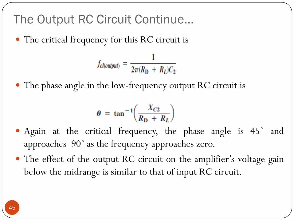
The Output RC Circuit Continue…
The critical frequency for this RC circuit is
The phase angle in the low-frequency output RC circuit is
Again at the critical frequency, the phase angle is 45˚ and
approaches 90˚ as the frequency approaches zero.
The effect of the output RC circuit on the amplifier’s voltage gain
below the midrange is similar to that of input RC circuit.
45

46

Reference(s)
47
Chapter 1O: “Electronic Devices”, by Thomas L .Floyd, 7th Edition.