aml8726-m3_qrm v1.0 20110706
TRANSCRIPT
AML8726‐M3 Quick Reference Manual Revision 1.0
AMLOGIC, Inc. Proprietary1/37
AML8726‐M3 Quick Reference Manual
Revision: 0.7 Release date: 10/31/2010 Printing date: 7/6/2011
Amlogic, Inc.
Distrib
ute
to P
rom
aste
r!

AML8726‐M3 Quick Reference Manual Revision 1.0
AMLOGIC, Inc. Proprietary2/37
COPYRIGHT © 2010 Amlogic, Inc. All rights reserved. No part of this document may be reproduced. Transmitted, transcribed, or translated into any language in any form or by any means with the written permission of Amlogic, Inc. TRADEMARKS AMLOGIC is a trademark of Amlogic, Inc. All other trademarks and registered trademarks are property of their respective companies. DISCLAIMER Amlogic Inc. may make improvements and/or changes in this document or in the product described in this document at any time. This product is not intended for use in medical, life saving, or life sustaining applications. Circuit diagrams and other information relating to products of Amlogic Inc. are included as a means or illustrating typical applications. Consequently, complete information sufficient for production design is not necessarily given. Amlogic makes no representations or warranties with respect to the accuracy or completeness of the contents presented in this document. REVISION HISTORY
Revision Number
Revision Date Changes
0.7 2011/06/17 Initial draft 1.0 2011/06/30 Revise Pin‐out
CONTACT INFORMATION Amlogic, Inc. 3930 Freedom Circle, Suite 101 Santa Clara, CA 95054 U.S.A. www.amlogic.com
Distrib
ute
to P
rom
aste
r!

AML8726‐M3 Quick Reference Manual Revision 1.0
AMLOGIC, Inc. Proprietary3/37
Contents 1. General Description .............................................................................................................................. 4
2. Features Summary ................................................................................................................................ 5
3. Pin Out Specification ............................................................................................................................ 9
Pin‐Out Diagram (top view) ...................................................................................................................... 9
3.1 Pin Assignments ................................................................................................................................ 10
3.2 Pin Multiplexing Tables ..................................................................................................................... 21
4. Operating Conditions .......................................................................................................................... 35
5. Mechanical Dimensions ...................................................................................................................... 36
Distrib
ute
to P
rom
aste
r!

AML8726‐M3 Quick Reference Manual Revision 1.0
AMLOGIC, Inc. Proprietary4/37
1. General Description AML8726‐M3 is an advanced connected multimedia processor designed for Tablet/MID, Set Top Box (STB), TV and high‐end
media player applications. It integrates powerful CPU/GPU, and a state‐of‐the‐art video decoding engine with all major
peripherals to form the ultimate low power multimedia SoC.
The integrated processor is an ARM Cortex‐A9 CPU with 32KB L1 instruction and 32K data cache and a large 128KB L2 unified
cache to improve system performance. In addition, the Cortex‐A9 CPU includes the NEON SIMD co‐processor to improve
software media processing capability. The ARM Cortex‐A9 CPU can run up to 1GHz and has a wide bus connecting to the
memory sub‐system.
The graphic subsystem consists of two graphic engines and a flexible video/graphic output pipeline. The ARM Mali‐400 GPU
handles all the OpenGL ES 1.1/2.0 and OpenVG graphics programs, while the 2.5D graphics processor handles additional
scaling, alpha, rotation and color space conversion operations. The video output pipeline can perform advanced image
correction and enhancements. Together, the CPU and GPU handle all operating system, networking, user‐interface and
gaming related tasks.
Three additional processors offload the Cortex‐A9 CPU by handling all audio and video decoding processing – the MediaCPU
and two MediaDSPs with a dedicated hardware video decoders. The MediaCPU is audio optimized and handles all audio
decoding tasks. The dual MediaDSPs with hardware decoder can decode all HD video formats including H.264, MVC, MPEG‐
1/2/4, VC‐1/WMV, AVS, RealVideo and MJPEG streams. The video decoding engine is also capable of decoding JPEG pictures
with no size limitation.
AML8726‐M3 integrates complete audio/video input/output interfaces including LVDS/mini‐LVDS panel interface with TCON,
RGB888 TTL panel interface with TCON, an HDMI1.4a transmitter with 3D support, CEC and PHY, four video DAC supporting
composite, CVBS, YPbPr and VGA output, a complete audio CODEC with headphone PA and microphone bias, I2S and SPDIF
digital audio input/output interface, a PCM audio interface and an ITU601/656 camera input interface.
AML8726‐M3 integrates a set of functional blocks for digital TV broadcasting streams. The build‐in three demux can process
the TV streams from three transport stream input interfaces, which can connect to tuner/demodulator. An ISO7816 smart
card interface and a crypto‐processor build in to help handling encrypted traffic and media streams.
The processor has rich advanced network and peripheral interfaces, including a 10/100 Fast Ethernet MAC with RMII
interface, dual USB 2.0 high speed ports (one OTG and one HOST), two SDIO with multi‐standard memory card controller,
four UART interface, four I2C interface, two high‐speed SPI interface and two PWMs.
Standard development environment utilizing GNU/GCC Android tool chain is supported. Please contact your AMLOGIC sales
representative for more information.
Dis
trib
ute
to P
rom
aste
r!

AML8726‐M3 Quick Reference Manual Revision 1.0
AMLOGIC, Inc. Proprietary5/37
2. Features Summary
CPU Sub‐system
• ARM Cortex‐A9 CPU up to 1GHz frequency and 2500DMIPS
• ARMv7 instruction set, multi‐issue superscalar, out‐of‐order architecture
• 32KB instruction cache and 32KB data cache
• 128KB Unified L2 cache
• Advanced NEON and VFP co‐processor
• Memory Management Unit
• Application based traffic optimization using internal QoS‐based switching fabrics 3D Graphics Processing Unit
• ARM Mali‐400 GPU, 250MHz
• Unified 32KB cache to reduce graphic data bandwidth
• 250Mpix/sec and 25Mtri/sec
• Full scene over‐sampled 4X anti‐aliasing engine with no additional bandwidth usage
• OpenGL ES 1.1/2.0 and OpenVG 1.1 support 2.5D Graphics Processor
De-
inte
rlace
r
Scal
ar
Enha
ncem
ent
Aud
io IF
Distrib
ute
to P
rom
aste
r!

AML8726‐M3 Quick Reference Manual Revision 1.0
AMLOGIC, Inc. Proprietary6/37
• Fast bitblt engine with dual inputs and single output
• Programmable raster operations (ROP)
• Programmable polyphase scaling filter
• Supports multiple video formats 4:2:0, 4:2:2 and 4:4:4 and multiple pixel formats (8/16/24/32 bits graphics layer)
• Fast color space conversion
• Advanced anti‐flickering filter Crypto Engine
• Supports AES block cipher with 128/192/256 bits keys, standard 16 bytes block size and streaming
• Supports DES/3DES block cipher with Electronic Code Book (ECB) and Cipher Block Chaining (CBC) operation mode
• Supports standard 64 bits key for DES and 192 bits key for 3DES
• Support streaming decoder with standard 64 bits block size
• Build‐in LSFR Random number generator Video/Picture Decoder
• Dual programmable DSP engines at 200MHz with DSP instructions
• Dedicated hardware video decoder
• H.264 [email protected] up to 1080P, MVC at 30Hz
• MPEG‐4 Part 2 ASP up to 1080P (ISO‐14496‐2)
• WMV/VC‐1 SP/MP/AP up to 1080P
• AVS JiZhun Profile up to 1080P
• MPEG‐2 MP/HL up to 1080P (ISO‐13818)
• MPEG‐1 MP/HL up to 1080P (ISO‐11172)
• RealVideo 8/9/10 up to 720P
• WebM up to VGA
• Multiple language and multiple format sub‐title video support
• Supports *.mkv,*.wmv,*.mpg, *.mpeg, *.dat, *.avi, *.mov, *.iso, *.mp4, *.rm and *.jpg file formats
• MJPEG and JPEG unlimited pixel resolution decoding (ISO/IEC‐10918)
• Supports JPEG thumbnail, scaling, rotation and transition effects Video Post‐Processing Controller
• Motive adaptive 3D noise reduction filter
• Advanced motion adaptive edge enhancing de‐interlacing engine
• 3:2 pull‐down support
• Programmable poly‐phase scalar for both horizontal and vertical dimension for zoom and windowing
• Programmable color management filter (to enhance blue, green, red, face and other colors)
• Chroma coring and black extension processing
• Dynamic Non‐Linear Luma filter
• Programmable color matrix pipeline
• Video mixer: 2 video planes and 2 graphics planes Digital LCD Panel Output
• TTL and LVDS/mini‐LVDS panel supporting
• Single port LVDS/mini‐LVDS with TCON supporting both single and dual‐gate panels up to 1366x768 resolution
• RGB888 TTL interface with TCON supporting digital panel up to 1920x1200 resolution
• LED BL PWM and VGHL PWM build‐in
• Three independent Gamma table for LCD panel tuning
• Dithering logic for mapping to different LCD panel color depth
Distrib
ute
to P
rom
aste
r!

AML8726‐M3 Quick Reference Manual Revision 1.0
AMLOGIC, Inc. Proprietary7/37
Video Output
• Build‐in HDMI 1.4a transmitter with CEC, both controller and PHY
• Programmable 4 channels high speed video DACs for analog video output including CVBS, S‐Video, YPbPr and VGA
• Supports all standard SD/HD video output formats: 480i/p, 576i/p, 720p and 1080i/p
• Supports dual video output with combination of LCD+HDMI, TTL+LVDS or CVBS+HDMI Audio Decoder and Input/Output
• MediaCPU with DSP audio processing
• Supports MP3, AAC, WMA, RM, LFAC, Ogg and programmable with 7.1 down‐mixing
• Build‐in 2 channels audio DAC with headphone power amplifier
• Stereo headphone output and mono speaker output
• I2S , SPDIF/IEC958 and PCM serial digital audio output
• Supports concurrent dual audio stereo channel output with combination of Analog+PCM or I2S+PCM Other Digital Audio/Video Input/Output Interfaces
• ITU 601/656 parallel video input with down‐scalar
• Supports camera input as YUV422, RGB565, 10bit rawRGB ,16bit RGB or JPEG Memory and Storage Interface
• Supports DDR3‐1066 SDRAM with 32‐bit data bus
• Supports up to 2GB DDR3 memory
• Supports SLC/MLC/TLC NAND Flash with 4 chip enable pins with BCH60
• Supports serial NOR Flash via SPI interface
• Build‐in One‐Time‐Programming ROM for key storage
• SDIO with memory card controller with 8‐bit data bus supporting SD/SDHC/SDXC/MMC/MS/MS‐Pro memory cards Network
• Integrated IEEE 802.3 10/100 Fast Ethernet controller with RMII interface
• 50MHz clock output to Fast Ethernet PHY
• WiFi/IEEE802.11 supporting via SDIO/USB Digital Television Interface
• Three transport stream(TS) input interfaces with three build‐in demux processor for connecting to external digital TV tuner/demodulator and one output TS interface
• Build‐in PWM, I2C and SPI interfaces to control tuner and demodulator
• CI+ PCMCIA controller and interface
• Integrated ISO 7816 smart card controller Integrated I/O Controllers and Interfaces
• Dual USB 2.0 high‐speed USB I/O, one USB Host and one USB Device
• Four UART Interface with RTS/CTS,one in AO domain
• 4x I2C master/slave interface,2x in AO domain
• High speed bi‐directional SPI interface with 3 slave select signals
• 2x PWM channel with feedback control logic and 4x simple PWM channel
• Programmable IR remote controller
• Build‐in 10bit SAR ADC with 8 input channels with resistive touch panel controller
• A set of General Purpose IO interfaces
Distrib
ute
to P
rom
aste
r!

AML8726‐M3 Quick Reference Manual Revision 1.0
AMLOGIC, Inc. Proprietary8/37
System, Peripherals and Misc. Interfaces
• Multiple power domain
• Dedicated always‐on (AO) power domain to communicate with external PMIC
• Integrated general purpose timers, counters, DMA controllers
• Integrated RTC with battery backup option
• Single 24 MHz crystal oscillator input
• Embedded debug interface using ICE/JTAG
• AMPOWER power management circuits supporting multiple sleep and suspend operating modes Software
• Supports Android and Linux operating systems
• Supports Adobe Flash Player 10.x
• GNU/GCC Android tools chain Package
• 445‐ball LFBGA, RoHS compliant, 17x17mm
Distrib
ute
to P
rom
aste
r!

AML8726‐M3 Quick Reference Manual Revision 1.0
AMLOGIC, Inc. Proprietary9/37
3. Pin Out Specification
Pin‐Out Diagram (top view)
Distrib
ute
to P
rom
aste
r!

AML8726‐M3 Quick Reference Manual Revision 1.0
AMLOGIC, Inc. Proprietary10/37
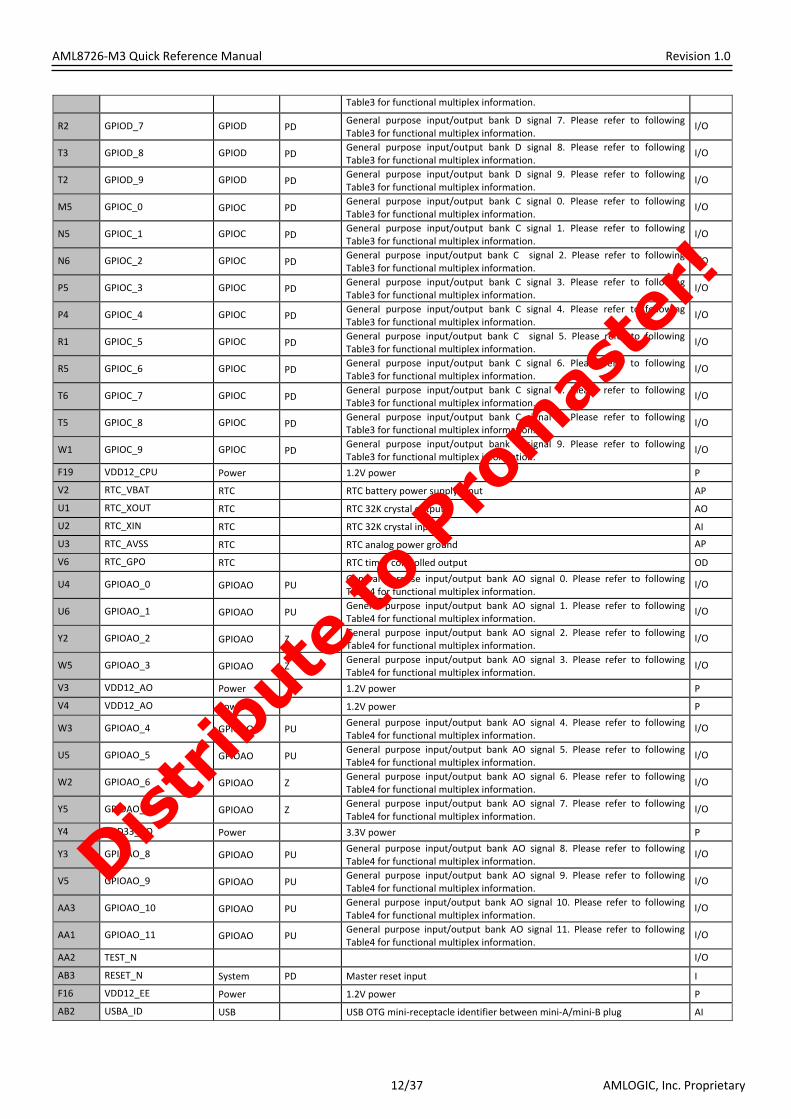
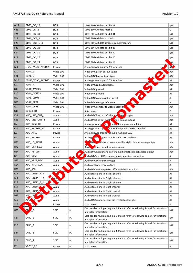
3.1 Pin Assignments The AML8726‐M3 A/V processor pin assignment is described in the following table.
Table 1. Pin Name assignments
BGA Ball
Pin Name Group Pull‐up/down
Description Type
A5 GPIOA_0 GPIOA PU
General purpose input/output bank A signal 0. Please refer to following Table2 for functional multiplex information.
I/O
B5 GPIOA_1 GPIOA PU General purpose input/output bank A signal 1. Please refer to following Table2 for functional multiplex information.
I/O
C4 GPIOA_2 GPIOA PU General purpose input/output bank A signal 2. Please refer to following Table2 for functional multiplex information.
I/O
B4 GPIOA_3 GPIOA PU General purpose input/output bank A signal 3. Please refer to following Table2 for functional multiplex information.
I/O
D4 GPIOA_4 GPIOA PU General purpose input/output bank A signal 4. Please refer to following Table2 for functional multiplex information.
I/O
A3 GPIOA_5 GPIOA PU General purpose input/output bank A signal 5. Please refer to following Table2 for functional multiplex information.
I/O
B3 GPIOA_6 GPIOA PU General purpose input/output bank A signal 6. Please refer to following Table2 for functional multiplex information.
I/O
A2 GPIOA_7 GPIOA PU General purpose input/output bank A signal 7. Please refer to following Table2 for functional multiplex information.
I/O
A1 GPIOA_8 GPIOA PU General purpose input/output bank A signal 8. Please refer to following Table2 for functional multiplex information.
I/O
B2 GPIOA_9 GPIOA PU General purpose input/output bank A signal 9. Please refer to following Table2 for functional multiplex information.
I/O
B1 GPIOA_10 GPIOA PU General purpose input/output bank A signal 10. Please refer to following Table2 for functional multiplex information.
I/O
C3 GPIOA_11 GPIOA PU General purpose input/output bank A signal 11. Please refer to following Table2 for functional multiplex information.
I/O
F12 VDD33_EE Power 3.3V power P
E15 VDD12_CPU Power 1.2V power P
C1 GPIOA_12 GPIOA PU General purpose input/output bank A signal 12. Please refer to following Table2 for functional multiplex information.
I/O
C2 GPIOA_13 GPIOA PU General purpose input/output bank A signal 13. Please refer to following Table2 for functional multiplex information.
I/O
D3 GPIOA_14 GPIOA PU General purpose input/output bank A signal 14. Please refer to following Table2 for functional multiplex information.
I/O
D2 GPIOA_15 GPIOA PU General purpose input/output bank A signal 15. Please refer to following Table2 for functional multiplex information.
I/O
E3 GPIOA_16 GPIOA PU General purpose input/output bank A signal 16. Please refer to following Table2 for functional multiplex information.
I/O
E1 GPIOA_17 GPIOA PU General purpose input/output bank A signal 17. Please refer to following Table2 for functional multiplex information.
I/O
E2 GPIOA_18 GPIOA PU General purpose input/output bank A signal 18. Please refer to following Table2 for functional multiplex information.
I/O
F3 GPIOA_19 GPIOA PU General purpose input/output bank A signal 19. Please refer to following Table2 for functional multiplex information.
I/O
D5 GPIOA_20 GPIOA PU General purpose input/output bank A signal 20. Please refer to following Table2 for functional multiplex information.
I/O
E5 GPIOA_21 GPIOA PU General purpose input/output bank A signal 21. Please refer to following Table2 for functional multiplex information.
I/O
E4 GPIOA_22 GPIOA PU General purpose input/output bank A signal 22. Please refer to following Table2 for functional multiplex information.
I/O
F4 GPIOA_23 GPIOA PU General purpose input/output bank A signal 23. Please refer to following Table2 for functional multiplex information.
I/O
F5 GPIOA_24 GPIOA PU General purpose input/output bank A signal 24. Please refer to following Table2 for functional multiplex information.
I/O
G5 GPIOA_25 GPIOA PU General purpose input/output bank A signal 25. Please refer to following Table2 for functional multiplex information.
I/O
G6 GPIOA_26 GPIOA PU General purpose input/output bank A signal 26. Please refer to following Table2 for functional multiplex information.
I/O
G1 GPIOA_27 GPIOA PU General purpose input/output bank A signal 27. Please refer to following I/O
Distrib
ute
to P
rom
aste
r!

AML8726‐M3 Quick Reference Manual Revision 1.0
AMLOGIC, Inc. Proprietary11/37
Table2 for functional multiplex information.
F2 GPIOB_0 GPIOB PD General purpose input/output bank B signal 0. Please refer to following Table2 for functional multiplex information.
I/O
G3 GPIOB_1 GPIOB PD General purpose input/output bank B signal 1. Please refer to following Table2 for functional multiplex information.
I/O
H5 GPIOB_2 GPIOB PD General purpose input/output bank B signal 2. Please refer to following Table2 for functional multiplex information.
I/O
G2 GPIOB_3 GPIOB PD General purpose input/output bank B signal 3. Please refer to following Table2 for functional multiplex information.
I/O
H3 GPIOB_4 GPIOB PD General purpose input/output bank B signal 4. Please refer to following Table2 for functional multiplex information.
I/O
H2 GPIOB_5 GPIOB PD General purpose input/output bank B signal 5. Please refer to following Table2 for functional multiplex information.
I/O
J3 GPIOB_6 GPIOB PD General purpose input/output bank B signal 6. Please refer to following Table2 for functional multiplex information.
I/O
J1 GPIOB_7 GPIOB PD General purpose input/output bank B signal 7. Please refer to following Table2 for functional multiplex information.
I/O
F15 VDD12_EE Power 1.2V power P
F17 VDD12_CPU Power 1.2V power P
F11 VDD33_EE Power 3.3V power P
H4 GPIOB_8 GPIOB PD General purpose input/output bank B signal 8. Please refer to following Table2 for functional multiplex information.
I/O
J4 GPIOB_9 GPIOB PD General purpose input/output bank B signal 9. Please refer to following Table2 for functional multiplex information.
I/O
K6 GPIOB_10 GPIOB PD General purpose input/output bank B signal 10. Please refer to following Table2 for functional multiplex information.
I/O
K5 GPIOB_11 GPIOB PD General purpose input/output bank B signal 11. Please refer to following Table2 for functional multiplex information.
I/O
L6 GPIOB_12 GPIOB PD General purpose input/output bank B signal 12. Please refer to following Table2 for functional multiplex information.
I/O
L5 GPIOB_13 GPIOB PD General purpose input/output bank B signal 13. Please refer to following Table2 for functional multiplex information.
I/O
L4 GPIOB_14 GPIOB PD General purpose input/output bank B signal 14. Please refer to following Table2 for functional multiplex information.
I/O
M4 GPIOB_15 GPIOB PD General purpose input/output bank B signal 15. Please refer to following Table2 for functional multiplex information.
I/O
J2 GPIOB_16 GPIOB PD General purpose input/output bank B signal 16. Please refer to following Table2 for functional multiplex information.
I/O
K3 GPIOB_17 GPIOB PD General purpose input/output bank B signal 17. Please refer to following Table2 for functional multiplex information.
I/O
K2 GPIOB_18 GPIOB PD General purpose input/output bank B signal 18. Please refer to following Table2 for functional multiplex information.
I/O
L3 GPIOB_19 GPIOB PD General purpose input/output bank B signal 19. Please refer to following Table2 for functional multiplex information.
I/O
F18 VDD12_CPU Power 1.2V power P
L1 GPIOB_20 GPIOB PD General purpose input/output bank B signal 20. Please refer to following Table2 for functional multiplex information.
I/O
L2 GPIOB_21 GPIOB PD General purpose input/output bank B signal 21. Please refer to following Table2 for functional multiplex information.
I/O
M3 GPIOB_22 GPIOB PD General purpose input/output bank B signal 22. Please refer to following Table2 for functional multiplex information.
I/O
M2 GPIOB_23 GPIOB PD General purpose input/output bank B signal 23. Please refer to following Table2 for functional multiplex information.
I/O
F6 VDD33_EE Power 3.3V power P
N3 GPIOD_0 GPIOD PD General purpose input/output bank D signal 0. Please refer to following Table3 for functional multiplex information.
I/O
N1 GPIOD_1 GPIOD PD General purpose input/output bank D signal 1. Please refer to following Table3 for functional multiplex information.
I/O
N2 GPIOD_2 GPIOD PD General purpose input/output bank D signal 2. Please refer to following Table3 for functional multiplex information.
I/O
P2 GPIOD_3 GPIOD PD General purpose input/output bank D signal 3. Please refer to following Table3 for functional multiplex information.
I/O
P3 GPIOD_4 GPIOD PD General purpose input/output bank D signal 4. Please refer to following Table3 for functional multiplex information.
I/O
R3 GPIOD_5 GPIOD PD General purpose input/output bank D signal 5. Please refer to following Table3 for functional multiplex information.
I/O
R4 GPIOD_6 GPIOD PD General purpose input/output bank D signal 6. Please refer to following I/O
Distrib
ute
to P
rom
aste
r!
AML8726‐M3 Quick Reference Manual Revision 1.0
AMLOGIC, Inc. Proprietary12/37
Table3 for functional multiplex information.
R2 GPIOD_7 GPIOD PD General purpose input/output bank D signal 7. Please refer to following Table3 for functional multiplex information.
I/O
T3 GPIOD_8 GPIOD PD General purpose input/output bank D signal 8. Please refer to following Table3 for functional multiplex information.
I/O
T2 GPIOD_9 GPIOD PD General purpose input/output bank D signal 9. Please refer to following Table3 for functional multiplex information.
I/O
M5 GPIOC_0 GPIOC PD General purpose input/output bank C signal 0. Please refer to following Table3 for functional multiplex information.
I/O
N5 GPIOC_1 GPIOC PD General purpose input/output bank C signal 1. Please refer to following Table3 for functional multiplex information.
I/O
N6 GPIOC_2 GPIOC PD General purpose input/output bank C signal 2. Please refer to following Table3 for functional multiplex information.
I/O
P5 GPIOC_3 GPIOC PD General purpose input/output bank C signal 3. Please refer to following Table3 for functional multiplex information.
I/O
P4 GPIOC_4 GPIOC PD General purpose input/output bank C signal 4. Please refer to following Table3 for functional multiplex information.
I/O
R1 GPIOC_5 GPIOC PD General purpose input/output bank C signal 5. Please refer to following Table3 for functional multiplex information.
I/O
R5 GPIOC_6 GPIOC PD General purpose input/output bank C signal 6. Please refer to following Table3 for functional multiplex information.
I/O
T6 GPIOC_7 GPIOC PD General purpose input/output bank C signal 7. Please refer to following Table3 for functional multiplex information.
I/O
T5 GPIOC_8 GPIOC PD General purpose input/output bank C signal 8. Please refer to following Table3 for functional multiplex information.
I/O
W1 GPIOC_9 GPIOC PD General purpose input/output bank C signal 9. Please refer to following Table3 for functional multiplex information.
I/O
F19 VDD12_CPU Power 1.2V power P
V2 RTC_VBAT RTC RTC battery power supply input AP
U1 RTC_XOUT RTC RTC 32K crystal output AO
U2 RTC_XIN RTC RTC 32K crystal input AI
U3 RTC_AVSS RTC RTC analog power ground AP
V6 RTC_GPO RTC RTC timer controlled output OD
U4 GPIOAO_0 GPIOAO PU General purpose input/output bank AO signal 0. Please refer to following Table4 for functional multiplex information.
I/O
U6 GPIOAO_1 GPIOAO PU General purpose input/output bank AO signal 1. Please refer to following Table4 for functional multiplex information.
I/O
Y2 GPIOAO_2 GPIOAO Z General purpose input/output bank AO signal 2. Please refer to following Table4 for functional multiplex information.
I/O
W5 GPIOAO_3 GPIOAO Z General purpose input/output bank AO signal 3. Please refer to following Table4 for functional multiplex information.
I/O
V3 VDD12_AO Power 1.2V power P
V4 VDD12_AO Power 1.2V power P
W3 GPIOAO_4 GPIOAO PU General purpose input/output bank AO signal 4. Please refer to following Table4 for functional multiplex information.
I/O
U5 GPIOAO_5 GPIOAO PU General purpose input/output bank AO signal 5. Please refer to following Table4 for functional multiplex information.
I/O
W2 GPIOAO_6 GPIOAO Z General purpose input/output bank AO signal 6. Please refer to following Table4 for functional multiplex information.
I/O
Y5 GPIOAO_7 GPIOAO Z General purpose input/output bank AO signal 7. Please refer to following Table4 for functional multiplex information.
I/O
Y4 VDD33_AO Power 3.3V power P
Y3 GPIOAO_8 GPIOAO PU General purpose input/output bank AO signal 8. Please refer to following Table4 for functional multiplex information.
I/O
V5 GPIOAO_9 GPIOAO PU General purpose input/output bank AO signal 9. Please refer to following Table4 for functional multiplex information.
I/O
AA3 GPIOAO_10 GPIOAO PU General purpose input/output bank AO signal 10. Please refer to following Table4 for functional multiplex information.
I/O
AA1 GPIOAO_11 GPIOAO PU General purpose input/output bank AO signal 11. Please refer to following Table4 for functional multiplex information.
I/O
AA2 TEST_N I/O
AB3 RESET_N System PD Master reset input I
F16 VDD12_EE Power 1.2V power P
AB2 USBA_ID USB USB OTG mini‐receptacle identifier between mini‐A/mini‐B plug AI
Distrib
ute
to P
rom
aste
r!
AML8726‐M3 Quick Reference Manual Revision 1.0
AMLOGIC, Inc. Proprietary13/37
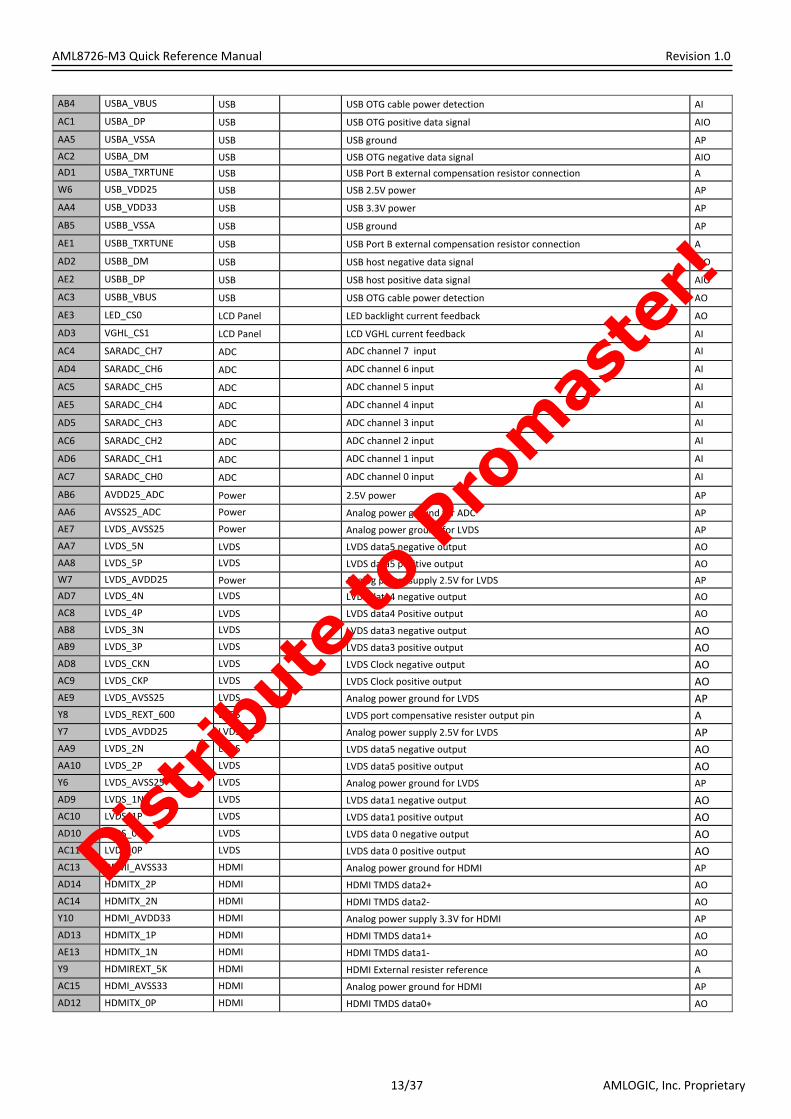
AB4 USBA_VBUS USB USB OTG cable power detection AI
AC1 USBA_DP USB USB OTG positive data signal AIO
AA5 USBA_VSSA USB USB ground AP
AC2 USBA_DM USB USB OTG negative data signal AIO AD1 USBA_TXRTUNE USB USB Port B external compensation resistor connection A
W6 USB_VDD25 USB USB 2.5V power AP
AA4 USB_VDD33 USB USB 3.3V power AP
AB5 USBB_VSSA USB USB ground AP
AE1 USBB_TXRTUNE USB USB Port B external compensation resistor connection A
AD2 USBB_DM USB USB host negative data signal AIO
AE2 USBB_DP USB USB host positive data signal AIO
AC3 USBB_VBUS USB USB OTG cable power detection AO
AE3 LED_CS0 LCD Panel LED backlight current feedback AO
AD3 VGHL_CS1 LCD Panel LCD VGHL current feedback AI
AC4 SARADC_CH7 ADC ADC channel 7 input AI
AD4 SARADC_CH6 ADC ADC channel 6 input AI
AC5 SARADC_CH5 ADC ADC channel 5 input AI
AE5 SARADC_CH4 ADC ADC channel 4 input AI
AD5 SARADC_CH3 ADC ADC channel 3 input AI
AC6 SARADC_CH2 ADC ADC channel 2 input AI
AD6 SARADC_CH1 ADC ADC channel 1 input AI
AC7 SARADC_CH0 ADC ADC channel 0 input AI
AB6 AVDD25_ADC Power 2.5V power AP
AA6 AVSS25_ADC Power Analog power ground for ADC AP
AE7 LVDS_AVSS25 Power Analog power ground for LVDS AP
AA7 LVDS_5N LVDS LVDS data5 negative output AO
AA8 LVDS_5P LVDS LVDS data5 positive output AO
W7 LVDS_AVDD25 Power Analog power supply 2.5V for LVDS AP
AD7 LVDS_4N LVDS LVDS data4 negative output AO
AC8 LVDS_4P LVDS LVDS data4 Positive output AO
AB8 LVDS_3N LVDS LVDS data3 negative output AO AB9 LVDS_3P LVDS LVDS data3 positive output AO AD8 LVDS_CKN LVDS LVDS Clock negative output AO AC9 LVDS_CKP LVDS LVDS Clock positive output AO AE9 LVDS_AVSS25 LVDS Analog power ground for LVDS AP Y8 LVDS_REXT_600 LVDS LVDS port compensative resister output pin A Y7 LVDS_AVDD25 LVDS Analog power supply 2.5V for LVDS AP AA9 LVDS_2N LVDS LVDS data5 negative output AO AA10 LVDS_2P LVDS LVDS data5 positive output AO Y6 LVDS_AVSS25 LVDS Analog power ground for LVDS AP
AD9 LVDS_1N LVDS LVDS data1 negative output AO AC10 LVDS_1P LVDS LVDS data1 positive output AO AD10 LVDS_0N LVDS LVDS data 0 negative output AO AC11 LVDS_0P LVDS LVDS data 0 positive output AO AC13 HDMI_AVSS33 HDMI Analog power ground for HDMI AP
AD14 HDMITX_2P HDMI HDMI TMDS data2+ AO
AC14 HDMITX_2N HDMI HDMI TMDS data2‐ AO
Y10 HDMI_AVDD33 HDMI Analog power supply 3.3V for HDMI AP
AD13 HDMITX_1P HDMI HDMI TMDS data1+ AO
AE13 HDMITX_1N HDMI HDMI TMDS data1‐ AO
Y9 HDMIREXT_5K HDMI HDMI External resister reference A
AC15 HDMI_AVSS33 HDMI Analog power ground for HDMI AP
AD12 HDMITX_0P HDMI HDMI TMDS data0+ AO
Distrib
ute
to P
rom
aste
r!
AML8726‐M3 Quick Reference Manual Revision 1.0
AMLOGIC, Inc. Proprietary14/37
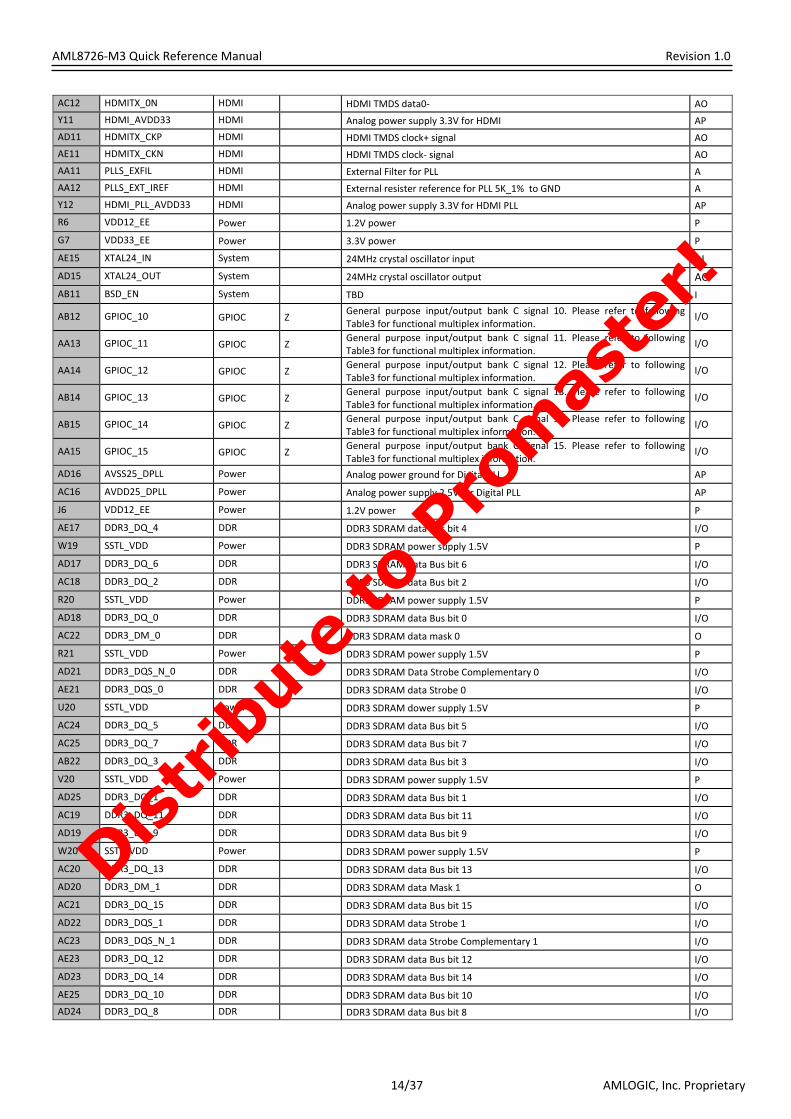
AC12 HDMITX_0N HDMI HDMI TMDS data0‐ AO
Y11 HDMI_AVDD33 HDMI Analog power supply 3.3V for HDMI AP
AD11 HDMITX_CKP HDMI HDMI TMDS clock+ signal AO
AE11 HDMITX_CKN HDMI HDMI TMDS clock‐ signal AO
AA11 PLLS_EXFIL HDMI External Filter for PLL A
AA12 PLLS_EXT_IREF HDMI External resister reference for PLL 5K_1% to GND A
Y12 HDMI_PLL_AVDD33 HDMI Analog power supply 3.3V for HDMI PLL AP
R6 VDD12_EE Power 1.2V power P
G7 VDD33_EE Power 3.3V power P
AE15 XTAL24_IN System 24MHz crystal oscillator input AI AD15 XTAL24_OUT System 24MHz crystal oscillator output AO AB11 BSD_EN System TBD I
AB12 GPIOC_10 GPIOC Z General purpose input/output bank C signal 10. Please refer to following Table3 for functional multiplex information.
I/O
AA13 GPIOC_11 GPIOC Z General purpose input/output bank C signal 11. Please refer to following Table3 for functional multiplex information.
I/O
AA14 GPIOC_12 GPIOC Z General purpose input/output bank C signal 12. Please refer to following Table3 for functional multiplex information.
I/O
AB14 GPIOC_13 GPIOC Z General purpose input/output bank C signal 13. Please refer to following Table3 for functional multiplex information.
I/O
AB15 GPIOC_14 GPIOC Z General purpose input/output bank C signal 14. Please refer to following Table3 for functional multiplex information.
I/O
AA15 GPIOC_15 GPIOC Z General purpose input/output bank C signal 15. Please refer to following Table3 for functional multiplex information.
I/O
AD16 AVSS25_DPLL Power Analog power ground for Digital PLL AP
AC16 AVDD25_DPLL Power Analog power supply 2.5V for Digital PLL AP
J6 VDD12_EE Power 1.2V power P
AE17 DDR3_DQ_4 DDR DDR3 SDRAM data Bus bit 4 I/O
W19 SSTL_VDD Power DDR3 SDRAM power supply 1.5V P
AD17 DDR3_DQ_6 DDR DDR3 SDRAM data Bus bit 6 I/O
AC18 DDR3_DQ_2 DDR DDR3 SDRAM data Bus bit 2 I/O
R20 SSTL_VDD Power DDR3 SDRAM power supply 1.5V P
AD18 DDR3_DQ_0 DDR DDR3 SDRAM data Bus bit 0 I/O
AC22 DDR3_DM_0 DDR DDR3 SDRAM data mask 0 O
R21 SSTL_VDD Power DDR3 SDRAM power supply 1.5V P
AD21 DDR3_DQS_N_0 DDR DDR3 SDRAM Data Strobe Complementary 0 I/O
AE21 DDR3_DQS_0 DDR DDR3 SDRAM data Strobe 0 I/O
U20 SSTL_VDD Power DDR3 SDRAM dower supply 1.5V P
AC24 DDR3_DQ_5 DDR DDR3 SDRAM data Bus bit 5 I/O
AC25 DDR3_DQ_7 DDR DDR3 SDRAM data Bus bit 7 I/O
AB22 DDR3_DQ_3 DDR DDR3 SDRAM data Bus bit 3 I/O
V20 SSTL_VDD Power DDR3 SDRAM power supply 1.5V P
AD25 DDR3_DQ_1 DDR DDR3 SDRAM data Bus bit 1 I/O
AC19 DDR3_DQ_11 DDR DDR3 SDRAM data Bus bit 11 I/O
AD19 DDR3_DQ_9 DDR DDR3 SDRAM data Bus bit 9 I/O
W20 SSTL_VDD Power DDR3 SDRAM power supply 1.5V P
AC20 DDR3_DQ_13 DDR DDR3 SDRAM data Bus bit 13 I/O
AD20 DDR3_DM_1 DDR DDR3 SDRAM data Mask 1 O
AC21 DDR3_DQ_15 DDR DDR3 SDRAM data Bus bit 15 I/O
AD22 DDR3_DQS_1 DDR DDR3 SDRAM data Strobe 1 I/O
AC23 DDR3_DQS_N_1 DDR DDR3 SDRAM data Strobe Complementary 1 I/O
AE23 DDR3_DQ_12 DDR DDR3 SDRAM data Bus bit 12 I/O
AD23 DDR3_DQ_14 DDR DDR3 SDRAM data Bus bit 14 I/O
AE25 DDR3_DQ_10 DDR DDR3 SDRAM data Bus bit 10 I/O
AD24 DDR3_DQ_8 DDR DDR3 SDRAM data Bus bit 8 I/O
Distrib
ute
to P
rom
aste
r!

AML8726‐M3 Quick Reference Manual Revision 1.0
AMLOGIC, Inc. Proprietary15/37
AC17 DDR3_VREF DDR DDR3 SDRAM reference voltage A Y16 DDR3_PZQ DDR Reference pin for ZQ calibration A AB23 DDR3_CK DDR DDR3 SDRAM Port A clock output O AB24 DDR3_CK_B DDR DDR3 SDRAM Port A clock output complementary O AA16 DDR3_RAS_B DDR Row Address Strobe O
Y17 DDR3_ODT1 DDR On‐die termination 1 O
AA17 DDR3_ODT0 DDR On‐die termination 0 O
M21 VDD12_EE Power 1.2V power P
AB17 DDR3_CAS_B DDR Column Address Strobe O
AB18 DDR3_CS1_B DDR DDR3 SDRAM port B chip select output 1 O
AA18 DDR3_WE_B DDR Write Enable O
Y19 DDR3_BA_2 DDR DDR3 SDRAM bank address 2 O
AA19 DDR3_A_2 DDR DDR3 SDRAM address bus bit 2 O
AA20 DDR3_A_9 DDR DDR3 SDRAM address bus bit 9 O
AB20 DDR3_A_7 DDR DDR3 SDRAM address bus bit 7 O
AB21 DDR3_A_13 DDR DDR3 SDRAM address bus bit 13 O
AA21 DDR3_A_5 DDR DDR3 SDRAM address bus bit 5 O AA22 DDR3_A_0 DDR DDR3 SDRAM address Bus bit 0 O
Y22 DDR3_A_3 DDR DDR3 SDRAM address Bus bit 3 O
Y21 DDR3_BA_0 DDR DDR3 SDRAM bank address 0 O
W21 DDR3_CS0_B DDR DDR3 SDRAM port B chip select output 0 O
V21 DDR3_A_8 DDR DDR3 SDRAM address bus bit 8 O
V22 DDR3_A_14 DDR DDR3 SDRAM address bus bit 14 O
U22 DDR3_A_6 DDR DDR3 SDRAM address bus bit 6 O
U21 DDR3_A_11 DDR DDR3 SDRAM address bus bit 11 O
T21 DDR3_A_1 DDR DDR3 SDRAM address bus bit 1 O
T20 DDR3_A_4 DDR DDR3 SDRAM address bus bit 4 O
R22 DDR3_A_12 DDR DDR3 SDRAM address bus bit 12 O
P22 DDR3_BA_1 DDR DDR3 SDRAM bank address 1 O
P21 DDR3_A_15 DDR DDR3 SDRAM address bus bit 15 O
N21 DDR3_A_10 DDR DDR3 SDRAM address bus bit 10 O
P20 DDR3_RST_B DDR DDR3 SDRAM Reset. Active LOW. O L22 DDR3_RET_N DDR DDR3 standby control input. LOW is Standby. HIGH is normal I
N20 DDR3_CKE_0 DDR DDR3 SDRAM clock enable output 0 O
M22 DDR3_CKE_1 DDR DDR3 SDRAM clock enable output 1 O
M24 DDR3_CK_1 DDR DDR3 SDRAM Port B clock output O
L23 DDR3_CK_1_N DDR DDR3 SDRAM Port B clock output 1 complementary O
Y14 VDD12_EE Power Digital power supply 1.2V P
AA23 DDR3_DQ_20 DDR DDR3 SDRAM data bus bit 20 I/O
AA24 DDR3_DQ_22 DDR DDR3 SDRAM data bus bit 22 I/O
Y23 DDR3_DQ_18 DDR DDR3 SDRAM data bus bit 18 I/O
Y24 DDR3_DQ_16 DDR DDR3 SDRAM data bus bit 16 I/O
T23 DDR3_DM_2 DDR DDR3 SDRAM data mask 2 O
U24 DDR3_DQS_N_2 DDR DDR3 SDRAM data strobe 2 complementary I/O
U25 DDR3_DQS_2 DDR DDR3 SDRAM data strobe 2 I/O
M23 DDR3_DQ_21 DDR DDR3 SDRAM data bus bit 21 I/O
N24 DDR3_DQ_23 DDR DDR3 SDRAM data bus bit 23 I/O
Y15 VDD12_EE Power Digital power supply 1.2V P
N25 DDR3_DQ_19 DDR DDR3 SDRAM data bus bit 19 I/O
N23 DDR3_DQ_17 DDR DDR3 SDRAM data bus bit 17 I/O
W23 DDR3_DQ_27 DDR DDR3 SDRAM data bus bit 27 I/O
W25 DDR3_DQ_25 DDR DDR3 SDRAM data bus bit 25 I/O
Distrib
ute
to P
rom
aste
r!
AML8726‐M3 Quick Reference Manual Revision 1.0
AMLOGIC, Inc. Proprietary16/37
W24 DDR3_DQ_29 DDR DDR3 SDRAM data bus bit 29 I/O
V23 DDR3_DM_3 DDR DDR3 SDRAM data mask 3 O
V24 DDR3_DQ_31 DDR DDR3 SDRAM data bus bit 31 I/O
T24 DDR3_DQS_3 DDR DDR3 SDRAM data strobe 3 I/O
R23 DDR3_DQS_N_3 DDR DDR3 SDRAM data strobe 3 complementary I/O
R25 DDR3_DQ_28 DDR DDR3 SDRAM data bus bit 28 I/O
R24 DDR3_DQ_30 DDR DDR3 SDRAM data bus bit 30 I/O
P23 DDR3_DQ_26 DDR DDR3 SDRAM data bus bit 26 I/O
P24 DDR3_DQ_24 DDR DDR3 SDRAM data bus bit 24 I/O
L20 EFUSE_VDAC_AVDD25 Power Analog power supply 2.5V for eFuse AP
L21 VDAC_G Video DAC Video DAC green output signal AO
K21 VDAC_B Video DAC Video DAC blue output signal AO
M20 EFUSE_VDAC_AVDD25 Power Analog power supply 2.5V for eFuse AP
J21 VDAC_R Video DAC Video DAC red output signal AO
J20 VDAC_AVSS25 Video DAC Video DAC ground AP
K20 VDAC_AVSS25 Video DAC Video DAC ground AP
H20 VDAC_COMP Video DAC Video DAC compensation signal A
G21 VDAC_REXT Video DAC Video DAC voltage reference A
J22 VDAC_CVBS Video DAC Video DAC composite video output signal AO
G19 VDD33_SD Power 3.3V power P
L24 AUD_LINE_OUT_L Audio Audio DAC line out left channel analog output AO
K23 AUD_LINE_OUT_R Audio Audio DAC line out right channel analog output AO
J24 AUD_AVSS_HS Power Analog power ground for headphone power amplifier AP
K24 AUD_AVDD25_HS Power Analog power supply 2.5V for headphone power amplifier AP
J23 AUD_AVSS Power Analog power ground for audio ADC and DAC AP
J25 AUD_AVDD25 Power Analog power supply 2.5V for audio ADC and DAC AP
H23 AUD_HS_RIGHT Audio Audio DAC headphone power amplifier right channel analog output AO
H22 AUD_MIC_BIAS Audio Biasing voltage output for microphone AO
H24 AUD_HS_LEFT Audio Audio DAC headphone power amplifier left channel analog output AO
G23 AUD_VCM Audio Audio DAC and ADC compensation capacitor connection A
G25 AUD_VREF_DAC Audio Audio DAC reference voltage A
G24 AUD_VREF_ADC Audio Audio ADC reference voltage A
H21 AUD_SPK‐ Audio Audio DAC mono speaker differential output minus AO
F23 AUD_LINEIN_R_3 Audio Audio stereo line in 3 right channel AI
F24 AUD_LINEIN_R_2 Audio Audio stereo line in 2 right channel AI
E23 AUD_LINEIN_R_1 Audio Audio stereo line in 1 right channel AI
E25 AUD_LINEIN_L_1 Audio Audio stereo line in 1 left channel AI
E24 AUD_LINEIN_L_2 Audio Audio stereo line in 2 left channel AI
D23 AUD_LINEIN_L_3 Audio Audio stereo line in 3 left channel AI
F20 AUD_SPK+ Audio Audio DAC mono speaker differential output plus AI
Y18 VDD12_EE Power 1.2V power P
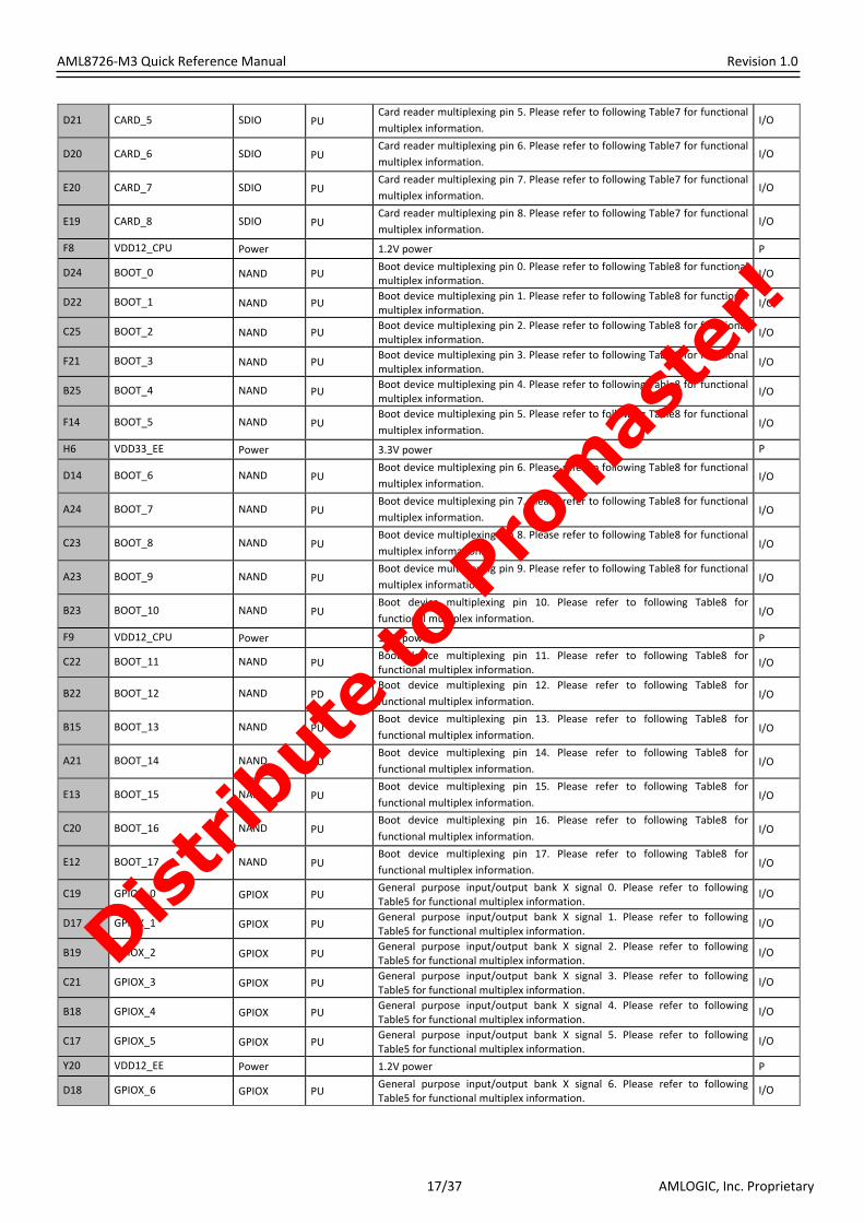
G20 CARD_0 SDIO PU Card reader multiplexing pin 0. Please refer to following Table7 for functional multiplex information.
I/O
C24 CARD_1 SDIO PU Card reader multiplexing pin 1. Please refer to following Table7 for functional multiplex information.
I/O
F22 CARD_2 SDIO PU Card reader multiplexing pin 2. Please refer to following Table7 for functional multiplex information.
I/O
B24 CARD_3 SDIO PU Card reader multiplexing pin 3. Please refer to following Table7 for functional multiplex information.
I/O
E21 CARD_4 SDIO PU Card reader multiplexing pin 4. Please refer to following Table7 for functional multiplex information.
I/O
F7 VDD12_CPU Power PU 1.2V power P
Distrib
ute
to P
rom
aste
r!
AML8726‐M3 Quick Reference Manual Revision 1.0
AMLOGIC, Inc. Proprietary17/37
D21 CARD_5 SDIO PU Card reader multiplexing pin 5. Please refer to following Table7 for functional multiplex information.
I/O
D20 CARD_6 SDIO PU Card reader multiplexing pin 6. Please refer to following Table7 for functional multiplex information.
I/O
E20 CARD_7 SDIO PU Card reader multiplexing pin 7. Please refer to following Table7 for functional multiplex information.
I/O
E19 CARD_8 SDIO PU Card reader multiplexing pin 8. Please refer to following Table7 for functional multiplex information.
I/O
F8 VDD12_CPU Power 1.2V power P
D24 BOOT_0 NAND PU Boot device multiplexing pin 0. Please refer to following Table8 for functional multiplex information.
I/O
D22 BOOT_1 NAND PU Boot device multiplexing pin 1. Please refer to following Table8 for functional multiplex information.
I/O
C25 BOOT_2 NAND PU Boot device multiplexing pin 2. Please refer to following Table8 for functional multiplex information.
I/O
F21 BOOT_3 NAND PU Boot device multiplexing pin 3. Please refer to following Table8 for functional multiplex information.
I/O
B25 BOOT_4 NAND PU Boot device multiplexing pin 4. Please refer to following Table8 for functional multiplex information.
I/O
F14 BOOT_5 NAND PU Boot device multiplexing pin 5. Please refer to following Table8 for functional multiplex information.
I/O
H6 VDD33_EE Power 3.3V power P
D14 BOOT_6 NAND PU Boot device multiplexing pin 6. Please refer to following Table8 for functional multiplex information.
I/O
A24 BOOT_7 NAND PU Boot device multiplexing pin 7. Please refer to following Table8 for functional multiplex information.
I/O
C23 BOOT_8 NAND PU Boot device multiplexing pin 8. Please refer to following Table8 for functional multiplex information.
I/O
A23 BOOT_9 NAND PU Boot device multiplexing pin 9. Please refer to following Table8 for functional multiplex information.
I/O
B23 BOOT_10 NAND PU Boot device multiplexing pin 10. Please refer to following Table8 for functional multiplex information.
I/O
F9 VDD12_CPU Power 1.2V power P
C22 BOOT_11 NAND PU Boot device multiplexing pin 11. Please refer to following Table8 for functional multiplex information.
I/O
B22 BOOT_12 NAND PD Boot device multiplexing pin 12. Please refer to following Table8 for functional multiplex information.
I/O
B15 BOOT_13 NAND PU Boot device multiplexing pin 13. Please refer to following Table8 for functional multiplex information.
I/O
A21 BOOT_14 NAND PU Boot device multiplexing pin 14. Please refer to following Table8 for functional multiplex information.
I/O
E13 BOOT_15 NAND PU Boot device multiplexing pin 15. Please refer to following Table8 for functional multiplex information.
I/O
C20 BOOT_16 NAND PU Boot device multiplexing pin 16. Please refer to following Table8 for functional multiplex information.
I/O
E12 BOOT_17 NAND PU Boot device multiplexing pin 17. Please refer to following Table8 for functional multiplex information.
I/O
C19 GPIOX_0 GPIOX PU General purpose input/output bank X signal 0. Please refer to following Table5 for functional multiplex information.
I/O
D17 GPIOX_1 GPIOX PU General purpose input/output bank X signal 1. Please refer to following Table5 for functional multiplex information.
I/O
B19 GPIOX_2 GPIOX PU General purpose input/output bank X signal 2. Please refer to following Table5 for functional multiplex information.
I/O
C21 GPIOX_3 GPIOX PU General purpose input/output bank X signal 3. Please refer to following Table5 for functional multiplex information.
I/O
B18 GPIOX_4 GPIOX PU General purpose input/output bank X signal 4. Please refer to following Table5 for functional multiplex information.
I/O
C17 GPIOX_5 GPIOX PU General purpose input/output bank X signal 5. Please refer to following Table5 for functional multiplex information.
I/O
Y20 VDD12_EE Power 1.2V power P
D18 GPIOX_6 GPIOX PU General purpose input/output bank X signal 6. Please refer to following Table5 for functional multiplex information.
I/O
Distrib
ute
to P
rom
aste
r!

AML8726‐M3 Quick Reference Manual Revision 1.0
AMLOGIC, Inc. Proprietary18/37
B17 GPIOX_7 GPIOX PU General purpose input/output bank X signal 7. Please refer to following Table5 for functional multiplex information.
I/O
C16 GPIOX_8 GPIOX PU General purpose input/output bank X signal 8. Please refer to following Table5 for functional multiplex information.
I/O
B16 GPIOX_9 GPIOX PU General purpose input/output bank X signal 9. Please refer to following Table5 for functional multiplex information.
I/O
C15 GPIOX_10 GPIOX PU General purpose input/output bank X signal 10. Please refer to following Table5 for functional multiplex information.
I/O
A15 GPIOX_11 GPIOX PU General purpose input/output bank X signal 11. Please refer to following Table5 for functional multiplex information.
I/O
C18 GPIOX_12 GPIOX PU General purpose input/output bank X signal 12. Please refer to following Table5 for functional multiplex information.
I/O
M6 VDD12_CPU Power 1.2V 1.2V power P
E18 GPIOX_13 GPIOX PU General purpose input/output bank X signal 13. Please refer to following Table5 for functional multiplex information.
I/O
A17 GPIOX_14 GPIOX PU General purpose input/output bank X signal 14. Please refer to following Table5 for functional multiplex information.
I/O
E22 GPIOX_15 GPIOX PU General purpose input/output bank X signal 15. Please refer to following Table5 for functional multiplex information.
I/O
A19 GPIOX_16 GPIOX PU General purpose input/output bank X signal 16. Please refer to following Table5 for functional multiplex information.
I/O
E16 GPIOX_17 GPIOX PU General purpose input/output bank X signal 17. Please refer to following Table5 for functional multiplex information.
I/O
A25 GPIOX_18 GPIOX PU General purpose input/output bank X signal 18. Please refer to following Table5 for functional multiplex information.
I/O
D15 GPIOX_19 GPIOX PU General purpose input/output bank X signal 19. Please refer to following Table5 for functional multiplex information.
I/O
A11 GPIOX_20 GPIOX PU General purpose input/output bank X signal 20. Please refer to following Table5 for functional multiplex information.
I/O
Y13 VDD33_EE Power 3.3V power P
E14 GPIOX_21 GPIOX PU General purpose input/output bank X signal 21. Please refer to following Table5 for functional multiplex information.
I/O
B21 GPIOX_22 GPIOX PU General purpose input/output bank X signal 22. Please refer to following Table5 for functional multiplex information.
I/O
F13 GPIOX_23 GPIOX PU General purpose input/output bank X signal 23. Please refer to following Table5 for functional multiplex information.
I/O
B20 GPIOX_24 GPIOX PU General purpose input/output bank X signal 24. Please refer to following Table5 for functional multiplex information.
I/O
D12 GPIOX_25 GPIOX PU General purpose input/output bank X signal 25. Please refer to following Table5 for functional multiplex information.
I/O
D11 GPIOX_26 GPIOX PU General purpose input/output bank X signal 26. Please refer to following Table5 for functional multiplex information.
I/O
E11 GPIOX_27 GPIOX PU General purpose input/output bank X signal 27. Please refer to following Table5 for functional multiplex information.
I/O
F10 GPIOX_28 GPIOX PU General purpose input/output bank X signal 28. Please refer to following Table5 for functional multiplex information.
I/O
P6 VDD12_CPU Power 1.2V power P
C14 GPIOX_29 GPIOX PU General purpose input/output bank X signal 29. Please refer to following Table5 for functional multiplex information.
I/O
E17 GPIOX_30 GPIOX PU General purpose input/output bank X signal 30. Please refer to following Table5 for functional multiplex information.
I/O
C13 GPIOX_31 GPIOX PU General purpose input/output bank X signal 31. Please refer to following Table5 for functional multiplex information.
I/O
B12 GPIOX_32 GPIOX PU General purpose input/output bank X signal 32. Please refer to following Table5 for functional multiplex information.
I/O
B13 GPIOX_33 GPIOX PU General purpose input/output bank X signal 33. Please refer to following Table5 for functional multiplex information.
I/O
C12 GPIOX_34 GPIOX PU General purpose input/output bank X signal 34. Please refer to following Table5 for functional multiplex information.
I/O
A13 GPIOX_35 GPIOX PU General purpose input/output bank X signal 35. Please refer to following Table5 for functional multiplex information.
I/O
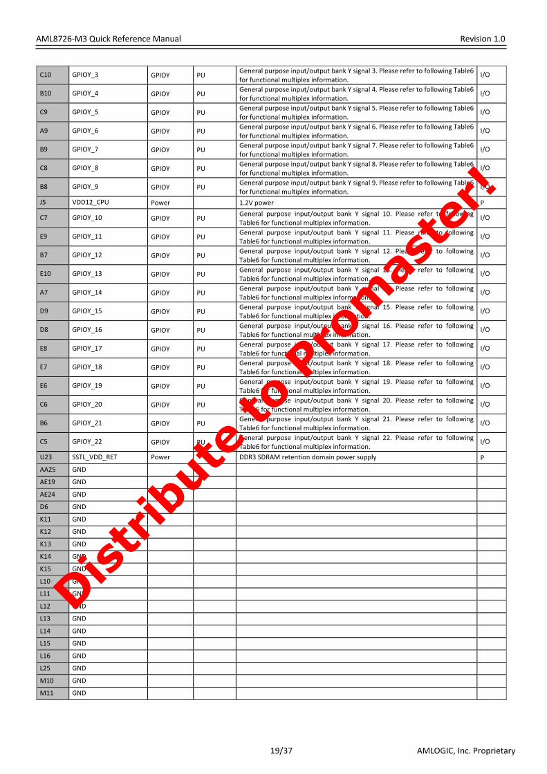
C11 GPIOY_0 GPIOY PU General purpose input/output bank Y signal 0. Please refer to following Table6for functional multiplex information.
I/O
B14 GPIOY_1 GPIOY PU General purpose input/output bank Y signal 1. Please refer to following Table6for functional multiplex information.
I/O
B11 GPIOY_2 GPIOY PU General purpose input/output bank Y signal 2. Please refer to following Table6for functional multiplex information.
I/O
Distrib
ute
to P
rom
aste
r!
AML8726‐M3 Quick Reference Manual Revision 1.0
AMLOGIC, Inc. Proprietary19/37
C10 GPIOY_3 GPIOY PU General purpose input/output bank Y signal 3. Please refer to following Table6for functional multiplex information.
I/O
B10 GPIOY_4 GPIOY PU General purpose input/output bank Y signal 4. Please refer to following Table6for functional multiplex information.
I/O
C9 GPIOY_5 GPIOY PU General purpose input/output bank Y signal 5. Please refer to following Table6for functional multiplex information.
I/O
A9 GPIOY_6 GPIOY PU General purpose input/output bank Y signal 6. Please refer to following Table6for functional multiplex information.
I/O
B9 GPIOY_7 GPIOY PU General purpose input/output bank Y signal 7. Please refer to following Table6for functional multiplex information.
I/O
C8 GPIOY_8 GPIOY PU General purpose input/output bank Y signal 8. Please refer to following Table6for functional multiplex information.
I/O
B8 GPIOY_9 GPIOY PU General purpose input/output bank Y signal 9. Please refer to following Table6for functional multiplex information.
I/O
J5 VDD12_CPU Power 1.2V power P
C7 GPIOY_10 GPIOY PU General purpose input/output bank Y signal 10. Please refer to following Table6 for functional multiplex information.
I/O
E9 GPIOY_11 GPIOY PU General purpose input/output bank Y signal 11. Please refer to following Table6 for functional multiplex information.
I/O
B7 GPIOY_12 GPIOY PU General purpose input/output bank Y signal 12. Please refer to following Table6 for functional multiplex information.
I/O
E10 GPIOY_13 GPIOY PU General purpose input/output bank Y signal 13. Please refer to following Table6 for functional multiplex information.
I/O
A7 GPIOY_14 GPIOY PU General purpose input/output bank Y signal 14. Please refer to following Table6 for functional multiplex information.
I/O
D9 GPIOY_15 GPIOY PU General purpose input/output bank Y signal 15. Please refer to following Table6 for functional multiplex information.
I/O
D8 GPIOY_16 GPIOY PU General purpose input/output bank Y signal 16. Please refer to following Table6 for functional multiplex information.
I/O
E8 GPIOY_17 GPIOY PU General purpose input/output bank Y signal 17. Please refer to following Table6 for functional multiplex information.
I/O
E7 GPIOY_18 GPIOY PU General purpose input/output bank Y signal 18. Please refer to following Table6 for functional multiplex information.
I/O
E6 GPIOY_19 GPIOY PU General purpose input/output bank Y signal 19. Please refer to following Table6 for functional multiplex information.
I/O
C6 GPIOY_20 GPIOY PU General purpose input/output bank Y signal 20. Please refer to following Table6 for functional multiplex information.
I/O
B6 GPIOY_21 GPIOY PU General purpose input/output bank Y signal 21. Please refer to following Table6 for functional multiplex information.
I/O
C5 GPIOY_22 GPIOY PU General purpose input/output bank Y signal 22. Please refer to following Table6 for functional multiplex information.
I/O
U23 SSTL_VDD_RET Power DDR3 SDRAM retention domain power supply P
AA25 GND
AE19 GND
AE24 GND
D6 GND
K11 GND
K12 GND
K13 GND
K14 GND
K15 GND
L10 GND
L11 GND
L12 GND
L13 GND
L14 GND
L15 GND
L16 GND
L25 GND
M10 GND
M11 GND
Distrib
ute
to P
rom
aste
r!

AML8726‐M3 Quick Reference Manual Revision 1.0
AMLOGIC, Inc. Proprietary20/37
M12 GND
M13 GND
M14 GND
M15 GND
M16 GND
N10 GND
N11 GND
N12 GND
N13 GND
N14 GND
N15 GND
N16 GND
P10 GND
P11 GND
P12 GND
P13 GND
P14 GND
P15 GND
P16 GND
R10 GND
R11 GND
R12 GND
R13 GND
R14 GND
R15 GND
R16 GND
T11 GND
T12 GND
T13 GND
T14 GND
T15 GND
Abbreviations:
• I = Digital input pin
• O = Digital output pin
• I/O = Digital input/output pin
• AI = Analog input pin
• AO = Analog output pin
• AIO = Analog input/output pin
• P = Power pin
• AP = Analog power pin
• NC = No connection
• PU=Pull‐Up
• PD=Pull‐down
• Z=Tri‐State
Distrib
ute
to P
rom
aste
r!

AML8726‐M3 Quick Reference Manual Revision 1.0
AMLOGIC, Inc. Proprietary21/37
3.2 Pin Multiplexing Tables Multiple usage pins are used to converse pin consumption for different features. The AML8726‐M3 devices can be used in many different applications but each application will not utilize all the on chip features. As a result, some of the features share the same pin. Most of the multiple usage pins can be used as a GPIO pin also.
Table 2. GPIOA_x and GPIOB_x Multi‐Function Pin Pin# Pin Name LCD Input FEC/ENCA5 GPIOA_0 LCDin_R0 FEC_D0_A
B5 GPIOA_1 LCDin_R1 FEC_D1_A
C4 GPIOA_2 LCDin_R2 FEC_D2_A
B4 GPIOA_3 LCDin_R3 FEC_D3_A/ FEC_D0_C
D4 GPIOA_4 LCDin_R4 FEC_D4_A/ FEC_CLK_C
A3 GPIOA_5 LCDin_R5 FEC_D5_A/ FEC_SOP_C
B3 GPIOA_6 LCDin_R6 FEC_D6_A/ FEC_D_VALID_C
A2 GPIOA_7 LCDin_R7 FEC_D7_A/ FEC_FAIL_C
A1 GPIOA_8 LCDin_G0 FEC_CLK_A
B2 GPIOA_9 LCDin_G1 FEC_SOP_A
B1 GPIOA_10 LCDin_G2 FEC_D_VALID_A
C3 GPIOA_11 LCDin_G3 FEC_FAIL_A
C1 GPIOA_12 LCDin_G4 ENC_0
C2 GPIOA_13 LCDin_G5 ENC_1
D3 GPIOA_14 LCDin_G6 ENC_2
D2 GPIOA_15 LCDin_G7 ENC_3
E3 GPIOA_16 LCDin_B0 ENC_4
E1 GPIOA_17 LCDin_B1 ENC_5
E2 GPIOA_18 LCDin_B2 ENC_6
F3 GPIOA_19 LCDin_B3 ENC_7
D5 GPIOA_20 LCDin_B4 ENC_8
E5 GPIOA_21 LCDin_B5 ENC_9
E4 GPIOA_22 LCDin_B6 ENC_10
F4 GPIOA_23 LCDin_B7 ENC_11
F5 GPIOA_24 LCDin_CLK ENC_12
G5 GPIOA_25 LCDin_HS ENC_13
G6 GPIOA_26 LCDin_VS ENC_14
G1 GPIOA_27 LCDin_DE ENC_15
F2 GPIOB_0 LCD_R0 FEC_D0_B
G3 GPIOB_1 LCD_R1 FEC_D1_B
H5 GPIOB_2 LCD_R2 FEC_D2_B
G2 GPIOB_3 LCD_R3 FEC_D3_B
H3 GPIOB_4 LCD_R4 FEC_D4_B
H2 GPIOB_5 LCD_R5 FEC_D5_B
J3 GPIOB_6 LCD_R6 FEC_D6_B
J1 GPIOB_7 LCD_R7 FEC_D7_B
H4 GPIOB_8 LCD_G0 FEC_CLK_B
J4 GPIOB_9 LCD_G1 FEC_SOP_B
K6 GPIOB_10 LCD_G2 FEC_D_VALID_B
K5 GPIOB_11 LCD_G3 FEC_FAIL_B
L6 GPIOB_12 LCD_G4 FEC_FAIL_OUT
L5 GPIOB_13 LCD_G5 FEC_D_VALID_OUT
L4 GPIOB_14 LCD_G6 FEC_SOP_OUT
M4 GPIOB_15 LCD_G7 FEC_CLK_OUT
J2 GPIOB_16 LCD_B0 FEC_D0_OUT
K3 GPIOB_17 LCD_B1 FEC_D1_OUT
K2 GPIOB_18 LCD_B2 FEC_D2_OUT
L3 GPIOB_19 LCD_B3 FEC_D3_OUT
Distrib
ute
to P
rom
aste
r!

AML8726‐M3 Quick Reference Manual Revision 1.0
AMLOGIC, Inc. Proprietary22/37
L1 GPIOB_20 LCD_B4 FEC_D4_OUT
L2 GPIOB_21 LCD_B5 FEC_D5_OUT
M3 GPIOB_22 LCD_B6 FEC_D6_OUT
M2 GPIOB_23 LCD_B7 FEC_D7_OUT
Table 3. GPIOC_x and GPIOD_x Multi‐Function pins
Pin#
Pin Name
LCD/LED
FEC/ENC
TCON
SPI/SPDIF
HDMI
CLK
PCM/PWM
VGA
N3 GPIOD_0 LCD_VGHL_PWM PWM_C
N1 GPIOD_1 LED_BL_PWM PWM_D
N2 GPIOD_2 TCON_0_B (LCD) / TCON_STH1_B
P2 GPIOD_3 TCON_1_B/ TCON_STV1_B
P3 GPIOD_4 TCON_2_B/ TCON_OEH_B
R3 GPIOD_5 TCON_3_B / TCON_CPV1_B
R4 GPIOD_6 TCON_4_B/ TCON_OEV1_B
R2 GPIOD_7 TCON_5_B / TCON_CPH50_B/ TCON_CPH1_B/
TCON_CPH2_B/ TCON_CPH3_B
T3 GPIOD_8 TCON_6_B / TCON_VCOM_B
T2 GPIOD_9 ENC_16 TCON_7_B PWM_A
M5 GPIOC_0 LCD_VGHL_PWM PWM_A VGA_HS
N5 GPIOC_1 LED_BL_PWM PWM_B VGA_VS
N6 GPIOC_2 TCON_0_A (mLVDS)/ TCON_STH1
P5 GPIOC_3 TCON_1_A/ TCON_STV1
P4 GPIOC_4 TCON_2_A/ TCON_OEH
R1 GPIOC_5 TCON_3_A/ TCON_CPV1
R5 GPIOC_6 TCON_4_A/ TCON_OEV1
T6 GPIOC_7 TCON_5_A/ TCON_CPH50/ TCON_CPH1/ TCON_CPH/
TCON_CPH3
T5 GPIOC_8 TCON_6_A/ TCON_VCOM SPDIF_IN
W1 GPIOC_9 ENC_17 TCON_7_A SPDIF_OUT PWM_C
AB12 GPIOC_10 HDMI_HPD (5V)
AA13 GPIOC_11 HDMI_SDA (5V)
AA14 GPIOC_12 HDMI_SCL (5V)
AB14 GPIOC_13 HDMI_CEC
AA15 GPIOC_15 CLK_OUT1 (XTAL, RTC,
PLL)
Distrib
ute
to P
rom
aste
r!

AML8726‐M3 Quick Reference Manual Revision 1.0
AMLOGIC, Inc. Proprietary23/37
Table 4. GPIOAO_x Multi‐Function pins
Pin#
Pin Name
UART I2C/I2S
JTAG
CLK
Remote
U4 GPIOAO_0 UART_TX_AO JTAG_TDO
U6 GPIOAO_1 UART_RX_AO JTAG_TDI
Y2 GPIOAO_2 UART_CTS_AO I2C_SCK_AO/ I2C_CLK_SLAVE_AO JTAG_TMS
W5 GPIOAO_3 UART_RTS_AO I2C_SDA_AO // I2C_SDA_SLAVE_AO JTAG_TCK
W3 GPIOAO_4 I2C_SCK_AO/ I2C_SCK_SLAVE_AO
U5 GPIOAO_5 I2C_SDA_AO/ I2C_SDA_SLAVE_AO
W2 GPIOAO_6 CLK_OUT2(XTAL, RTC, PLL)
Y5 GPIOAO_7 REMOTE_INPUT
Y3 GPIOAO_8 JTAG_TCK
V5 GPIOAO_9 JTAG_TMS
AA3 GPIOAO_10 JTAG_TDI
AA1 GPIOAO_11 JTAG_TDO CLK_OUT2(XTAL, RTC, PLL)
Distrib
ute
to P
rom
aste
r!

AML8726‐M3 Quick Reference Manual Revision 1.0
AMLOGIC, Inc. Proprietary24/37
Table 5. GPIOX_x Multi‐Function pins
Pin#
Pin Name
SPI/SPDIF
UART I2C/I2S
SD
ISO7816
PCM/PWM
C19 GPIOX_0 SDXC_D0_A /SD_D0_A
D17 GPIOX_1 I2S_OUT_CH67 SDXC_D1_A /SD_D1_A
B19 GPIOX_2 I2S_OUT_CH45 SDXC_D2_A /SD_D2_A
C21 GPIOX_3
I2S_OUT_CH23 SDXC_D3_A / SD_D3_A
B18 GPIOX_4 I2S_OUT_CH01 SDXC_D4_A PCM_OUT
C17 GPIOX_5 I2S_IN_CH01 SDXC_D5_A PCM_IN
D18 GPIOX_6 I2S_LR_CLK SDXC_D6_A
PCM_FS
B17 GPIOX_7 I2S_AM_CLK SDXC_D7_A
PCM_CLK
C16 GPIOX_8 SDXC_CLK_A /SD_CLK_A
B16 GPIOX_9 SDXC_CMD_A / SD_CMD_A
C15 GPIOX_10 SDXC_GPIO0_A
A15 GPIOX_11 SDXC_GPIO1_A
C18 GPIOX_12 I2S_AO_CLK SDXC_GPIO2_A
E18 GPIOX_13 UART_TX_A
A17 GPIOX_14 UART_RX_A
E22 GPIOX_15 UART_CTS_A
A19 GPIOX_16 UART_RTS_A
E16 GPIOX_17 UART_TX_B I2S_AM_CLK ISO7816_DET PCM_CLK
A25 GPIOX_18 UART_RX_B I2S_AO_CLK ISO7816_RESET PCM_FS
D15 GPIOX_19 UART_CTS_B I2S_LR_CLK ISO7816_CLK
A11 GPIOX_20 UART_RTS_B I2S_IN_CH01/I2S_OUT_CH01 ISO7816_DATA PCM_IN
E14 GPIOX_21 UART_TX_C ISO7816_DET
B21 GPIOX_22 UART_RX_C ISO7816_RESET
F13 GPIOX_23 UART_CTS_C / UART_TX_B ISO7816_CLK
B20 GPIOX_24 UART_RTS_C / UART_RX_B ISO7816_DATA
D12 GPIOX_25 I2C_SDA_A
D11 GPIOX_26 I2C_SCK_A
E11 GPIOX_27 I2C_SDA_B
F10 GPIOX_28 I2C_SCK_B
C14 GPIOX_29 SPI_SS2 I2C_SCK_C
E17 GPIOX_30 SPI_RDYn I2C_SDA_C
C13 GPIOX_31 SPI_SS0
B12 GPIOX_32 SPI_SS1
B13 GPIOX_33 SPI_SCLK
C12 GPIOX_34 SPI_MOSI
A13 GPIOX_35 SPI_MISO
Distrib
ute
to P
rom
aste
r!

AML8726‐M3 Quick Reference Manual Revision 1.0
AMLOGIC, Inc. Proprietary25/37
Table 6. GPIOY_x Multi‐Function pins
Pin#
Pin Name
RMII
ITU601
CLK
C11 GPIOY_0 RMII_CLK50_IN_OUT
B14 GPIOY_1 RMII_RX_ERR
B11 GPIOY_2 RMII_CRS_DV
C10 GPIOY_3 RMII_RX_DATA1
B10 GPIOY_4 RMII_RX_DATA0
C9 GPIOY_5 RMII_TX_EN
A9 GPIOY_6 RMII_TX_DATA1
B9 GPIOY_7 RMII_TX_DATA0
C8 GPIOY_8 RMII_MDC
B8 GPIOY_9 RMII_MDIO
C7 GPIOY_10 ITU601_FIR / ITU601_IDQ
E9 GPIOY_11 ITU601_HS
B7 GPIOY_12 ITU601_VS
E10 GPIOY_13 ITU601_D0
A7 GPIOY_14 ITU601_D1
D9 GPIOY_15 ITU601_D2
D8 GPIOY_16 ITU601_D3
E8 GPIOY_17 ITU601_D4
E7 GPIOY_18 ITU601_D5
E6 GPIOY_19 ITU601_D6
C6 GPIOY_20 ITU601_D7
B6 GPIOY_21 ITU601_CLK
C5 GPIOY_22 CLK_OUT0 (XTAL, RTC, PLL)
Distrib
ute
to P
rom
aste
r!

AML8726‐M3 Quick Reference Manual Revision 1.0
AMLOGIC, Inc. Proprietary26/37
Table 7. CARD_x Multi‐Function Pin Pin# Pin Name SDXC SDIO G20 CARD_0 SDXC_D0_B SD_D0_B C24 CARD_1 SDXC_D1_B SD_D1_B F22 CARD_2 SDXC_D2_B SD_D2_B B24 CARD_3 SDXC_D3_B SD_D3_B E21 CARD_4 SDXC_CLK_B SD_CLK_B D21 CARD_5 SDXC_CMD_B SD_CMD_B D20 CARD_6 SDXC_GPIO0_B ‐ E20 CARD_7 SDXC_GPIO1 ‐ E19 CARD_8 SDXC_GPIO2 ‐
Table 8. BOOT_x Multi‐Function Pin Pin# Pin Name NAND SDXC SDIO NOR_SPID24 BOOT_0 NAND_IO_0 SDXC_D0_C SD_D0_CD22 BOOT_1 NAND_IO_1 SDXC_D1_C SD_D1_CC25 BOOT_2 NAND_IO_2 SDXC_D2_C SD_D2_CF21 BOOT_3 NAND_IO_3 SDXC_D3_C SD_D3_CB25 BOOT_4 NAND_IO_4 SDXC_D4_C ‐F14 BOOT_5 NAND_IO_5 SDXC_D5_C ‐D14 BOOT_6 NAND_IO_6 SDXC_D6_C ‐A24 BOOT_7 NAND_IO_7 SDXC_D7_C ‐C23 BOOT_8 NAND_CE0(boot) ‐ ‐A23 BOOT_9 NAND_CE1 ‐ ‐B23 BOOT_10 NAND_CE2/NAND_RB0 SDXC_CMD_C SD_CMD_CC22 BOOT_11 NAND_CE3/NAND_BR1 SDXC_CLK_C(bootable) SD_CLK_CB22 BOOT_12 NAND_ALE ‐ ‐ SPI_NOR_D_AB15 BOOT_13 NAND_CLE ‐ ‐ SPI_NOR_Q_AE12 BOOT_14 NAND_WEn_CLK ‐ ‐ SPI_NOR_C_AE13 BOOT_15 NAND_REn_WR ‐ ‐ ‐C20 BOOT_16 NAND_DQS ‐ ‐ ‐E12 BOOT_17 ‐ ‐ ‐ SPI_NRO_CS_n_A
Distrib
ute
to P
rom
aste
r!

AML8726‐M3 Quick Reference Manual Revision 1.0
AMLOGIC, Inc. Proprietary27/37
4. Signal Description Table 9. LCD/LED Signal Description
Signal Name Type Description LCDin_R0 I Digital video input red bit 0 (LSB)
LCDin_R1 I Digital video input red bit 1
LCDin_R2 I Digital video input red bit 2
LCDin_R3 I Digital video input red bit 3
LCDin_R4 I Digital video input red bit 4
LCDin_R5 I Digital video input red bit 5
LCDin_R6 I Digital video input red bit 6
LCDin_R7 I Digital video input red bit 7 (MSB)
LCDin_G0 I Digital video input green bit 0 (LSB)
LCDin_G1 I Digital video input green bit 1
LCDin_G2 I Digital video input green bit 2
LCDin_G3 I Digital video input green bit 3
LCDin_G4 I Digital video input green bit 4
LCDin_G5 I Digital video input green bit 5
LCDin_G6 I Digital video input green bit 6
LCDin_G7 I Digital video input green bit 7 (MSB)
LCDin_B0 I Digital video input blue bit 0 (LSB)
LCDin_B1 I Digital video input blue bit 1
LCDin_B2 I Digital video input blue bit 2
LCDin_B3 I Digital video input blue bit 3
LCDin_B4 I Digital video input blue bit 4
LCDin_B5 I Digital video input blue bit 5
LCDin_B6 I Digital video input blue bit 6
LCDin_B7 I Digital video input blue bit 7 (MSB)
LCDin_CLK I Digital video input clock
LCDin_HS I Digital video input horizontal sync
LCDin_VS I Digital video input vertical sync
LCDin_DE I Digital video input data enable
LCD_R0 O TTL LCD data output red bit 0 (LSB)
LCD_R1 O TTL LCD data output red bit 1
LCD_R2 O TTL LCD data output red bit 2
LCD_R3 O TTL LCD data output red bit 3
LCD_R4 O TTL LCD data output red bit 4
LCD_R5 O TTL LCD data output red bit 5
LCD_R6 O TTL LCD data output red bit 6
LCD_R7 O TTL LCD data output red bit 7 (MSB)
LCD_G0 O TTL LCD data output green bit 0 (LSB)
LCD_G1 O TTL LCD data output green bit 1
LCD_G2 O TTL LCD data output green bit 2
LCD_G3 O TTL LCD data output green bit 3
LCD_G4 O TTL LCD data output green bit 4
LCD_G5 O TTL LCD data output green bit 5
LCD_G6 O TTL LCD data output green bit 6
LCD_G7 O TTL LCD data output green bit 7 (MSB)
LCD_B0 O TTL LCD data output blue bit 0 (LSB)
LCD_B1 O TTL LCD data output blue bit 1
LCD_B2 O TTL LCD data output blue bit 2
Distrib
ute
to P
rom
aste
r!

AML8726‐M3 Quick Reference Manual Revision 1.0
AMLOGIC, Inc. Proprietary28/37
Signal Name Type Description LCD_B3 O TTL LCD data output blue bit 3
LCD_B4 O TTL LCD data output blue bit 4
LCD_B5 O TTL LCD data output blue bit 5
LCD_B6 O TTL LCD data output blue bit 6
LCD_B7 O TTL LCD data output blue bit 7 (MSB)
LCD_VGHL_PWM O LCD panel VGHL tuning pulse width modulation signal outputLED_BL_PWM O LED backlight tuning pulse width modulation signal output
Table 10. FEC/ENC Interface Signal Description Signal Name Type Description FEC_D0_A I TS input port A data bus bit 0 (LSB)
FEC_D1_A I TS input port A data bus bit 1
FEC_D2_A I TS input port A data bus bit 2
FEC_D3_A/ FEC_D0_C I TS input port A data bus bit 3 Serial TS input data
FEC_D4_A/ FEC_CLK_C I TS input port A data bus bit 4 Serial TS input clock
FEC_D5_A/ FEC_SOP_C I TS input port A data bus bit 5 Serial TS start of stream signal
FEC_D6_A/ FEC_D_VALID_C I TS input port A data bus bit 6 Serial TS data valid signal
FEC_D7_A/ FEC_FAIL_C I TS input port A data bus bit 7 (MSB) Serial TS data failure signal
FEC_CLK_A I TS input port A clock
FEC_SOP_A I TS input port A start of stream signal
FEC_D_VALID_A I TS input port A date valid signal
FEC_FAIL_A I TS input port A data failure signal
FEC_D0_B I TS input port B data bus bit 0 (LSB)
FEC_D1_B I TS input port B data bus bit 1
FEC_D2_B I TS input port B data bus bit 2
FEC_D3_B I TS input port B data bus bit 3
FEC_D4_B I TS input port B data bus bit 4
FEC_D5_B I TS input port B data bus bit 5
FEC_D6_B I TS input port B data bus bit 6
FEC_D7_B I TS input port B data bus bit 7 (MSB)
FEC_CLK_B I TS input port B clock
FEC_SOP_B I TS input port B start of stream signal
FEC_D_VALID_B I TS input port B date valid signal
FEC_FAIL_B I TS input port B data failure signal
FEC_D0_OUT O TS output data bus bit 0 (LSB)
FEC_D1_OUT O TS output data bus bit 1
FEC_D2_OUT O TS output data bus bit 2
FEC_D3_OUT O TS output data bus bit 3
FEC_D4_OUT O TS output data bus bit 4
FEC_D5_OUT O TS output data bus bit 5
FEC_D6_OUT O TS output data bus bit 6
FEC_D7_OUT O TS output data bus bit 7 (MSB)
FEC_FAIL_OUT O TS output data failure signal
FEC_D_VALID_OUT O TS output data valid signal
FEC_SOP_OUT O TS output start of stream signal
FEC_CLK_OUT O TS output clock
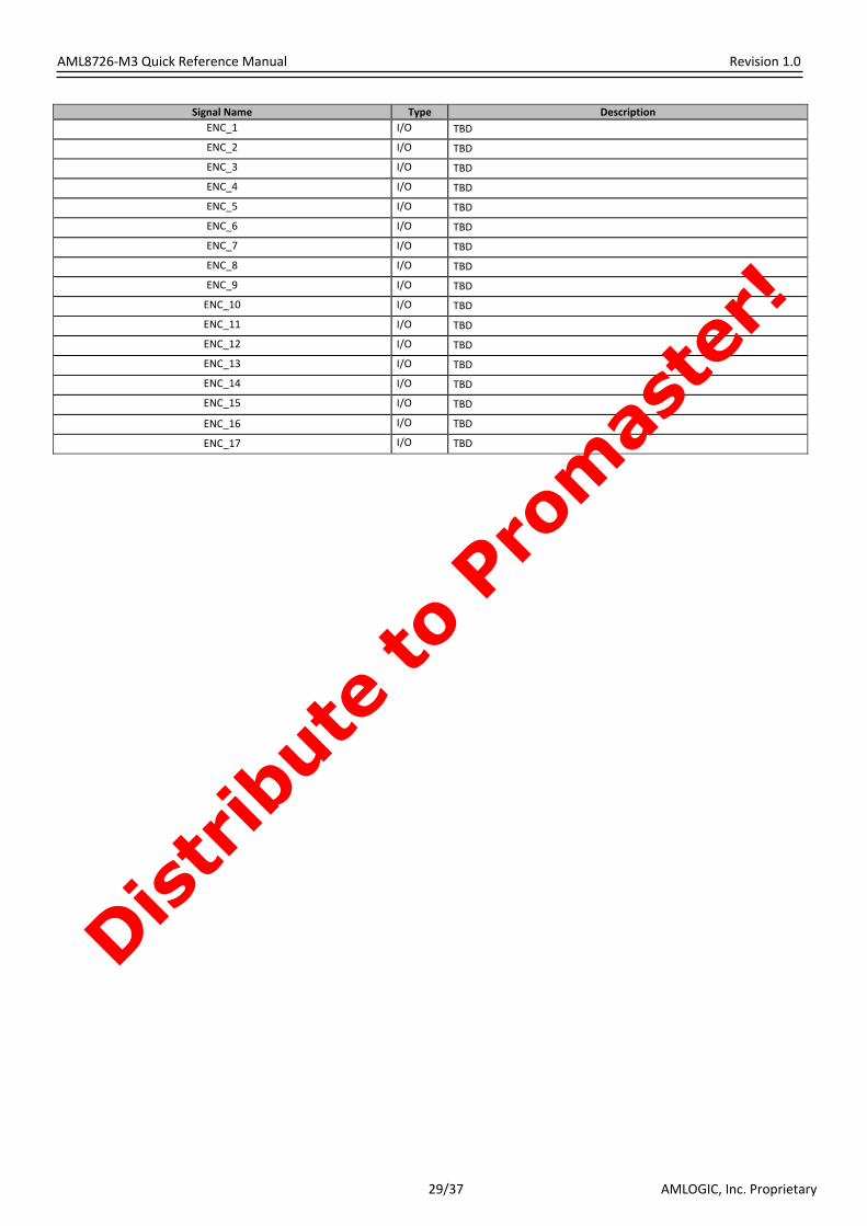
ENC_0 I/O TBD
Distrib
ute
to P
rom
aste
r!
AML8726‐M3 Quick Reference Manual Revision 1.0
AMLOGIC, Inc. Proprietary29/37
Signal Name Type Description ENC_1 I/O TBD
ENC_2 I/O TBD
ENC_3 I/O TBD
ENC_4 I/O TBD
ENC_5 I/O TBD
ENC_6 I/O TBD
ENC_7 I/O TBD
ENC_8 I/O TBD
ENC_9 I/O TBD
ENC_10 I/O TBD
ENC_11 I/O TBD
ENC_12 I/O TBD
ENC_13 I/O TBD
ENC_14 I/O TBD
ENC_15 I/O TBD
ENC_16 I/O TBD
ENC_17 I/O TBD
Distrib
ute
to P
rom
aste
r!

AML8726‐M3 Quick Reference Manual Revision 1.0
AMLOGIC, Inc. Proprietary30/37
Table 11. TCON Interface Signal Description Signal Name Type Description
TCON_0_B / TCON_STH1_B O Programmable TCON port B signal 0 for TTL LCD
TCON 1st source driver start pulse for TTL LCD
TCON_1_B/ TCON_STV1_B O Programmable TCON port B signal 1 for TTL LCD
TCON 1st gate driver start pulse for TTL LCD
TCON_2_B/ TCON_OEH_B O Programmable TCON port B signal 2 for TTL LCD
TCON output enable signal for source driver for TTL LCD
TCON_3_B / TCON_CPV1_B O Programmable TCON port B signal 3 for TTL LCD
TCON 1st gate driver shift clock output for TTL LCD
TCON_4_B/ TCON_OEV1_B O Programmable TCON port B signal 4 for TTL LCD
TCON output enable signal for 1st gate driver for TTL LCD
TCON_5_B / TCON_CPH50_B/ TCON_CPH1_B/ TCON_CPH2_B/ TCON_CPH3_B O Programmable TCON port B signal 5 for TTL LCD
TCON source driver shift clock output for TTL LCD
TCON_6_B / TCON_VCOM_B O Programmable TCON port B signal 6 for TTL LCD
TCON POL driving signal for TTL LCD
TCON_7_B O Programmable TCON port B signal 7 for TTL LCD
TCON_0_A / TCON_STH1 O Programmable TCON port A signal 0 for LVDS and mini‐LVDS
TCON_1_A/ TCON_STV1 O Programmable TCON port A signal 1 for MINILVDS
TCON_2_A/ TCON_OEH O Programmable TCON port A signal 2 for MINILVDS
TCON_3_A/ TCON_CPV1 O Programmable TCON port A signal 3 for MINILVDS
TCON_4_A/ TCON_OEV1 O Programmable TCON port A signal 4 for MINILVDS
TCON_5_A/ TCON_CPH50/ TCON_CPH1/ TCON_CPH/ TCON_CPH3 O Programmable TCON port A signal 5 for MINILVDS
TCON_6_A/ TCON_VCOM O Programmable TCON port A signal 6 for MINILVDS
TCON_7_A O Programmable TCON port A signal 7 for MINILVDS
Table 12. SPDIF Interface Signal Description Signal Name Type Description SPDIF_IN I SPDIF input signal
SPDIF_OUT O SPDIF output signal
Table 13. SPI IO Interface Signal Description
Signal Name Type Description SPI_SS2 O SPI slave select 2
SPI_RDYn I SPI Ready signal, low active
SPI_SS0 O SPI slave select 0
SPI_SS1 O SPI slave select 1
SPI_SCLK O SPI Serial Clock
SPI_MOSI O SPI Master Output, Slave Input
SPI_MISO I SPI Master Input, Slave Output
Dis
trib
ute
to P
rom
aste
r!

AML8726‐M3 Quick Reference Manual Revision 1.0
AMLOGIC, Inc. Proprietary31/37
Table 14. UART Interface Signal Description Signal Name Type Description UART_TX_AO O UART Port AO data output
UART_RX_AO I UART Port AO data input
UART_CTS_AO I UART Port AO Clear To Send Signal
UART_RTS_AO O UART Port AO Ready To Send Signal
UART_TX_A O UART Port A data output
UART_RX_A I UART Port A data input
UART_CTS_A I UART Port A Clear To Send Signal
UART_RTS_A O UART Port A Ready To Send Signal
UART_TX_B O UART Port B data output
UART_RX_B I UART Port B data input
UART_CTS_B I UART Port B Clear To Send Signal
UART_RTS_B O UART Port B Ready To Send Signal
UART_TX_C O UART Port C data output
UART_RX_C I UART Port C data input
UART_CTS_C / UART_TX_B I UART Port C Clear To Send Signal UART Port B data output
UART_RTS_C / UART_RX_B O UART Port C Clear To Send Signal UART Port B data input
Table 15. I2S Interface Signal Description Signal Name Type Description I2S_OUT_CH67 O I2S Audio Data Output channel 6 and 7
I2S_OUT_CH45 O I2S Audio Data Output channel 4 and 5
I2S_OUT_CH23 O I2S Audio Data Output channel 2 and 3
I2S_OUT_CH01 O I2S Audio Data Output channel 0 and 1
I2S_IN_CH01 I I2S Audio Data Input channel 0 and 1
I2S_LR_CLK O I2S Left/Right Clock Out
I2S_AM_CLK O I2S master clock output
I2S_AO_CLK O/I I2S data clock input/output
Table 16. I2C Interface Signal Description
Signal Name Type Description I2C_SCK_AO/ I2C_SCK_SLAVE_AO I/O Always‐on I2C serial clock line , Master or Slave, need pull high
I2C_SDA_AO/ I2C_SDA_SLAVE_AO I/O Always‐on I2C serial data line, Master or Slave, need pull high
I2C_SDA_A I/O I2C bus port A data input/output, Master or Slave, need pull high
I2C_SCK_A I/O I2C bus port A clock input/output, Master or Slave, need pull high
I2C_SDA_B I/O I2C bus port B data input/output, Master or Slave, need pull high
I2C_SCK_B I/O I2C bus port B clock input/output, Master or Slave, need pull high
I2C_SCK_C I/O I2C bus port C clock input/output, Master or Slave, need pull high
I2C_SDA_C I/O I2C bus port C clock input/output, Master or Slave, need pull high
Dis
trib
ute
to P
rom
aste
r!
AML8726‐M3 Quick Reference Manual Revision 1.0
AMLOGIC, Inc. Proprietary32/37
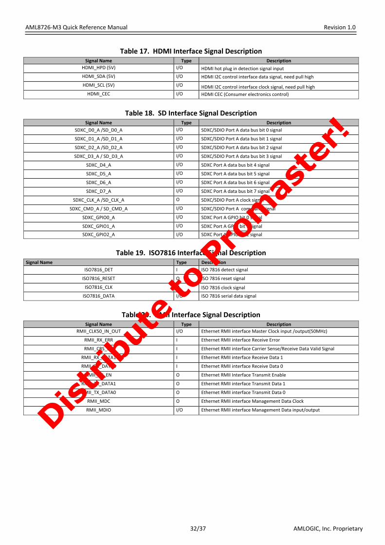
Table 17. HDMI Interface Signal Description Signal Name Type Description
HDMI_HPD (5V) I/O HDMI hot plug in detection signal input
HDMI_SDA (5V) I/O HDMI I2C control interface data signal, need pull high
HDMI_SCL (5V) I/O HDMI I2C control interface clock signal, need pull high HDMI_CEC I/O HDMI CEC (Consumer electronics control)
Table 18. SD Interface Signal Description Signal Name Type Description
SDXC_D0_A /SD_D0_A I/O SDXC/SDIO Port A data bus bit 0 signal
SDXC_D1_A /SD_D1_A I/O SDXC/SDIO Port A data bus bit 1 signal
SDXC_D2_A /SD_D2_A I/O SDXC/SDIO Port A data bus bit 2 signal
SDXC_D3_A / SD_D3_A I/O SDXC/SDIO Port A data bus bit 3 signal
SDXC_D4_A I/O SDXC Port A data bus bit 4 signal
SDXC_D5_A I/O SDXC Port A data bus bit 5 signal
SDXC_D6_A I/O SDXC Port A data bus bit 6 signal
SDXC_D7_A I/O SDXC Port A data bus bit 7 signal
SDXC_CLK_A /SD_CLK_A O SDXC/SDIO Port A clock signal
SDXC_CMD_A / SD_CMD_A I/O SDXC/SDIO Port A command signal
SDXC_GPIO0_A I/O SDXC Port A GPIO bit 0 signal
SDXC_GPIO1_A I/O SDXC Port A GPIO bit 1 signal
SDXC_GPIO2_A I/O SDXC Port A GPIO bit 2 signal
Table 19. ISO7816 Interface Signal Description Signal Name Type Description
ISO7816_DET I ISO 7816 detect signal
ISO7816_RESET O ISO 7816 reset signal
ISO7816_CLK O ISO 7816 clock signal
ISO7816_DATA I/O ISO 7816 serial data signal
Table 20. RMII Interface Signal Description Signal Name Type Description
RMII_CLK50_IN_OUT I/O Ethernet RMII interface Master Clock input /output(50MHz)
RMII_RX_ERR I Ethernet RMII interface Receive Error
RMII_CRS_DV I Ethernet RMII interface Carrier Sense/Receive Data Valid Signal
RMII_RX_DATA1 I Ethernet RMII interface Receive Data 1
RMII_RX_DATA0 I Ethernet RMII interface Receive Data 0
RMII_TX_EN O Ethernet RMII Interface Transmit Enable
RMII_TX_DATA1 O Ethernet RMII interface Transmit Data 1
RMII_TX_DATA0 O Ethernet RMII interface Transmit Data 0
RMII_MDC O Ethernet RMII interface Management Data Clock
RMII_MDIO I/O Ethernet RMII interface Management Data input/output
Distrib
ute
to P
rom
aste
r!

AML8726‐M3 Quick Reference Manual Revision 1.0
AMLOGIC, Inc. Proprietary33/37
Table 21. ITU601 Interface Signal Description Signal Name Type Description
ITU601_FIR / ITU601_IDQ I ITU 601 Video Input Field Signal
ITU601_HS I ITU 601 Video Input Horizontal Sync Signal
ITU601_VS I ITU 601 Video Input Vertical Sync Signal
ITU601_D0 I ITU 601 Video Input Data Bus bit 0 (LSB)
ITU601_D1 I ITU 601 Video Input Data Bus bit 1
ITU601_D2 I ITU 601 Video Input Data Bus bit 2
ITU601_D3 I ITU 601 Video Input Data Bus bit 3
ITU601_D4 I ITU 601 Video Input Data Bus bit 4
ITU601_D5 I ITU 601 Video Input Data Bus bit 5
ITU601_D6 I ITU 601 Video Input Data Bus bit 6
ITU601_D7 I ITU 601 Video Input Data Bus bit 7 (MSB)
ITU601_CLK I/O ITU 601 Video Input Master Clock
Table 22. JTAG Interface Signal Description Signal Name Type Description JTAG_TDO O JTAG Scan data output
JTAG_TDI I JTAG Scan data input
JTAG_TMS I JTAG Test mode select input
JTAG_TCK I JTAG Test clock input
Table 23. CLK Interface Signal Description Signal Name Type Description
CLK_OUT2(XTAL, RTC, PLL) O XTAL, RTC CLK, PLL clock output 2
CLK_OUT1 (XTAL, RTC, PLL) O XTAL, RTC CLK, PLL clock output 1
CLK_OUT0 (XTAL, RTC, PLL) O XTAL, RTC CLK, PLL clock output 0
Table 24. Remote Interface Signal Description Signal Name Type Description
REMOTE_INPUT I IR Remote controller input signal
Table 25. PWM Interface Signal Description Signal Name Type Description PWM_A O PWM channel A output signal
PWM_B O PWM channel B output signal
PWM_C O PWM channel C output signal
PWM_D O PWM channel D output signal
Distrib
ute
to P
rom
aste
r!
AML8726‐M3 Quick Reference Manual Revision 1.0
AMLOGIC, Inc. Proprietary34/37
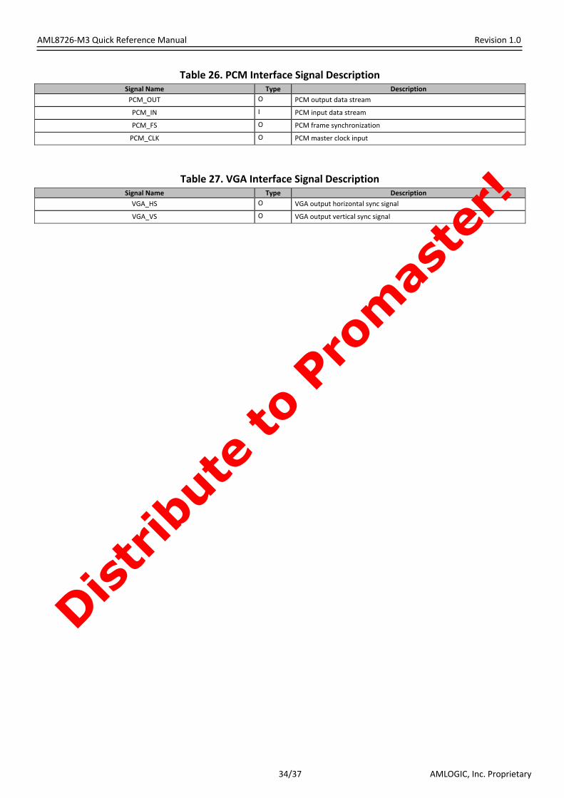
Table 26. PCM Interface Signal Description Signal Name Type Description PCM_OUT O PCM output data stream
PCM_IN I PCM input data stream
PCM_FS O PCM frame synchronization
PCM_CLK O PCM master clock input
Table 27. VGA Interface Signal Description Signal Name Type Description VGA_HS O VGA output horizontal sync signal
VGA_VS O VGA output vertical sync signal
Distrib
ute
to P
rom
aste
r!
AML8726‐M3 Quick Reference Manual Revision 1.0
AMLOGIC, Inc. Proprietary35/37
4. Operating Conditions Absolute Maximum Ratings The table below gives the absolute maximum ratings. Exposure to stresses beyond those listed in this table may result in permanent device damage, unreliability or both.
Characteristic Value Unit
1.2V Core Supply Voltage 1.4 V
1.5V Supply Voltage 1.65 V
2.5V Supply Voltage 2.75 V
3.3V Supply Voltage 3.63 V
Input voltage, VI ‐0.5 ~ VDD+0.3 V
Junction Temperature TBD °C
Recommended Operating Conditions Symbol Parameter Min. Typ. Max Unit
VDD(CORE) 1.2V Core Supply Voltage 1.14 1.2 1.32 V
VDD(SSTL) 1.5V SSTL Supply Voltage 1.35 1.5 1.65 V
VDD(AVDD) 2.5V AVDD Supply Voltage 2.38 2.5 2.75 V
VDD(IO) 3.3V IO Supply Voltage 3.14 3.3 3.63 V
TJ Junction Temperature 0 125 °C
DC Characteristics VDD = 3.3 +/‐ 0.3V, TA = 0 to 75°C
Symbol Parameters Condition Min Typ Max Unit
VIH High Level Input 2.0 3.3 V
VIL Low Level Input ‐0.3 0.8 V
VT+ Schmitt trigger, positive going Threshold 1.5 V VT‐ Schmitt trigger, negative going threshold 0.93
Voh High‐level output voltage Ioh = ‐2.0mA 2.4 V
Vol Low‐level output voltage Iol = 2.0 mA 0.4 V
Distrib
ute
to P
rom
aste
r!

AML8726‐M3 Quick Reference Manual Revision 1.0
AMLOGIC, Inc. Proprietary36/37
5. Mechanical Dimensions The AML8726‐M3 processor comes in a 445 balls LFBGA RoHS package. The mechanical dimensions are given in millimeters as below:
Distrib
ute
to P
rom
aste
r!

AML8726‐M3 Quick Reference Manual Revision 1.0
AMLOGIC, Inc. Proprietary37/37
Distrib
ute
to P
rom
aste
r!