all-optical switching with 1-ps response time in a ddmebt...
TRANSCRIPT
All-optical switching with 1-ps response time in a DDMEBT enabled silicon grating coupler/resonator hybrid device
John Covey,1,* Aaron D. Finke,3,6 Xiaochuan Xu,2 Wenzhi Wu,4 Yaguo Wang,5 François Diederich,3 and Ray T. Chen1
1Department of Electrical and Computer Engineering, The University of Texas at Austin, 10100 Burnet Rd, Austin, Texas 78758, USA
2Omega Optics, Inc, 10306 Sausalito Dr, Austin, Texas 78759, USA 3Laboratorium für Organische Chemie, ETH Zurich, Vladimir-Prelog-Weg 3, CH-8093 Zurich, Switzerland
4School of Electronic Engineering, Heilongjiang University, Harbin 150080, China 5Department of Mechanical Engineering, The University of Texas at Austin, 204 East Dean Keeton Street, Austin,
Texas 78712, USA [email protected]
Abstract: An amorphous film of the third-order nonlinear optical material DDMEBT was spun onto silicon chips for the first time, filling 80 nm lithographic features. A 710 μm2 device was designed, fabricated, and tested that acts both as a nonlinear resonator switch and as an input/output grating coupler to a perfectly vertical single mode fiber. Autocorrelation and spectral measurements indicate the device has <1 ps response time, 4 nm of switching bandwidth, and 4 dB of on/off contrast. With sufficient power, this all-optical device can potentially modulate a single optical carrier frequency in excess of 1 THz.
©2014 Optical Society of America
OCIS codes: (130.3120) Integrated optics devices; (230.1150) All-optical devices;(190.3270) Kerr effect; (320.7080) Ultrafast devices; (130.3130) Integrated optics materials; (230.5750) Resonators; (050.2770) Gratings.
References and links
1. L. G. Roberts, “Beyond Moore's law: Internet growth trends,” Computer 33(1), 117–119 (2000). 2. A. Martínez, J. Blasco, P. Sanchis, J. V. Galán, J. García-Rupérez, E. Jordana, P. Gautier, Y. Lebour, S.
Hernández, R. Guider, N. Daldosso, B. Garrido, J. M. Fedeli, L. Pavesi, J. Martí, and R. Spano, “Ultrafast All-Optical Switching in a Silicon-Nanocrystal-Based Silicon Slot Waveguide at Telecom Wavelengths,” Nano Lett. 10(4), 1506–1511 (2010).
3. J. Kerr, “On Rotation of the Plane of Polarization by Reflection from the Pole of a Magnet,” Philos. Mag. 3(3), 321–343 (1877).
4. K. Imakita, Y. Tsuchihashi, R. Naruiwa, M. Fujii, H. T. Sun, J. Qiu, and S. Hayashi, “Ultrafast nonlinear optical responses of bismuth doped silicon-rich silica films,” Appl. Phys. Lett. 101(19), 191106 (2012).
5. V. Mizrahi, K. W. Delong, G. I. Stegeman, M. A. Saifi, and M. J. Andrejco, “Two-photon absorption as a limitation to all-optical switching,” Opt. Lett. 14(20), 1140–1142 (1989).
6. B. L. Lawrence, M. Cha, J. U. Kang, W. Toruellas, G. Stegeman, G. Baker, J. Meth, and S. Etemad, “Large purely refractive nonlinear index of single crystal P-toluene sulphonate (PTS) at 1600 nm,” Electron. Lett. 30(5), 447–448 (1994).
7. S. Polyakov, F. Yoshino, M. Liu, and G. Stegeman, “Nonlinear refraction and multiphoton absorption in polydiacetylenes from 1200 to 2200 nm,” Phys. Rev. B 69(11), 115421 (2004).
8. M. Thakur and D. M. Krol, “Demonstration of all-optical phase modulation in polydiacetylene waveguides,” Appl. Phys. Lett. 56(13), 1213–1215 (1990).
9. S. H. Chi, J. M. Hales, C. Fuentes-Hernandez, S. Y. Tseng, J. Y. Cho, S. A. Odom, Q. Zhang, S. Barlow, R. R. Schrock, S. R. Marder, B. Kippelen, and J. W. Perry, “Thick Optical-Quality Films of Substituted Polyacetylenes with Large, Ultrafast Third-Order Nonlinearities and Application to Image Correlation,” Adv. Mater. 20(17), 3199–3203 (2008).
10. B. Esembeson, M. L. Scimeca, T. Michinobu, F. Diederich, and I. Biaggio, “A High-Optical Quality Supramolecular Assembly for Third-Order Integrated Nonlinear Optics,” Adv. Mater. 20(23), 4584–4587 (2008).
#221978 - $15.00 USD Received 2 Sep 2014; revised 22 Sep 2014; accepted 23 Sep 2014; published 30 Sep 2014(C) 2014 OSA 6 October 2014 | Vol. 22, No. 20 | DOI:10.1364/OE.22.024530 | OPTICS EXPRESS 24530

11. C. Koos, P. Vorreau, T. Vallaitis, P. Dumon, W. Bogaerts, R. Baets, B. Esembeson, I. Biaggio, T. Michinobu, F. Diederich, W. Freude, and J. Leuthold, “All-optical high-speed signal processing with silicon–organic hybrid slot waveguides,” Nat. Photonics 3(4), 216–219 (2009).
12. M. S. Fleischman, I. Biaggio, B. Breiten, and F. Diederich, “Dense Small Molecule Assemblies for Third-Order Nonlinear Optics: DDMEBT,” Lasers and Electro-Optics (CLEO), CTuL5 (2011).
13. D. Hall, P. Underhill, and J. M. Torkelson, “Spin Coating of Thin and Ultrathin Polymer Films,” Polym. Eng. Sci. 38(12), 2039–2045 (1998).
14. C. Y. Lin, X. Wang, S. Chakravarty, B. S. Lee, W. Lai, J. Luo, A. K.-Y. Jen, and R. T. Chen, “Electro-Optic Polymer Infiltrated Silicon Photonic Crystal Slot Waveguide Modulator with 23dB Slow Light Enhancement,” Appl. Phys. Lett. 97(9), 093304 (2010).
15. J. Covey and R. T. Chen, “Efficient perfectly vertical fiber-to-chip grating coupler for silicon horizontal multiple slot waveguides,” Opt. Express 21(9), 10886–10896 (2013).
16. C. Husko, A. De Rossi, S. Combrié, Q.-V. Tran, F. Raineri, and C. W. Wong, “Ultrafast all-optical modulation in GaAs photonic crystal cavities,” Appl. Phys. Lett. 94(2), 021111 (2009).
17. S. Gulde, A. Jebali, and N. Moll, “Optimization of ultrafast all-optical resonator switching,” Opt. Express 13(23), 9502–9515 (2005).
18. D. Aillaerta, F. Van Laere, M. Yre, W. Bogaerts, D. Van Thourhout, P. Bienstman, and R. Baets, “Grating Couplers for Coupling between Optical Fibers and Nanophotonic Waveguides,” Jap, J. Appl. Phys. 45(8A), 6071–6077 (2006).
19. C. Xu, J. M. Roth, W. H. Knox, and K. Bergman, “Ultra-Sensitive Autocorrelation of 1.5 Mu M Light with Single Photon Counting Silicon Avalanche Photodiode,” Electron. Lett. 38(2), 86–88 (2002).
20. H. C. Liu and A. Yariv, “Synthesis of high-order bandpass filters based on coupled-resonator optical waveguides (CROWs),” Opt. Express 19(18), 17653–17668 (2011).
21. B. E. Little, S. T. Chu, H. A. Haus, J. Foresi, and J. P. Laine, “Microring resonator channel dropping filters,” J. Lightwave Technol. 15(6), 998–1005 (1997).
22. H. S. Nalwa and S. Miyata, Nonlinear Optics of Organic Molecules and Polymers (CRC Press, Boca Raton, 1997), Chap. 12.
23. M. Dinu, F. Quochi, and H. Garcia, “Third-order nonlinearities in silicon at telecom wavelengths,” Appl. Phys. Lett. 82(18), 2954–2956 (2003).
24. C. Manolatou and M. Lipson, “All-Optical Silicon Modulators Based on Carrier Injection by Two-Photon Absorption,” J. Lightwave Technol. 24(3), 1433–1439 (2006).
1. Introduction
Even as the continuation of Moore's law comes in question, the increasing trend of network connections and bandwidth consumed is progressing exponentially with no foreseeable sign of halting [1]. As the need for higher bandwidth permeates core networks, data centers, board-to-board communications, and on-chip interconnects, switching heavy channels with electronic devices must be abandoned if speeds greater than 100 Gb/s are to be feasibly obtained. In order to accommodate the increased demand for bandwidth and data speed, high speed, all-optical switching of data must be increasingly adopted in the future. To further facilitate this transition, the relevant optical devices also need to be miniaturized as much as possible to minimize footprint and maximize bandwidth density, which are as important as overall switching speed.
To this end, silicon photonics is the most promising platform for future all-optical switching. The high index of refraction of silicon shrinks the effective wavelength within a device. The fabrication maturity of the silicon electronics industry can also be leveraged to rapidly and cheaply create a large number of optical devices with incredible economies of scale. The synergy of fabrication technologies may allow for silicon-based, all-optical devices to be integrable onto the back end of existing electronic chips, provided that optical designs accommodate this process flow.
Although 100 GHz all-optical switching has been demonstrated in a ring resonator on a silicon platform with silicon nanocrystals as the nonlinear medium, exotic deposition and high temperature annealing were required during fabrication. The device footprint was in excess of 1,600 μm2, which may be too large for future device requirements [2]. Although silicon nanocrystals possess a large nonlinear Kerr coefficient, they also exhibit substantial two-photon absorption, which degrades and distorts the material's switching capacity. Thus, it is desirable to demonstrate the upper limit of all-optical switching in a silicon platform where
#221978 - $15.00 USD Received 2 Sep 2014; revised 22 Sep 2014; accepted 23 Sep 2014; published 30 Sep 2014(C) 2014 OSA 6 October 2014 | Vol. 22, No. 20 | DOI:10.1364/OE.22.024530 | OPTICS EXPRESS 24531
switching speed is maximized, a standard silicon platform is utilized, fabrication is as simple as possible, and footprint is kept to a minimum.
In this work, high speed all-optical switching is demonstrated on a standard silicon-on-insulator (SOI) platform. A third-order nonlinear optical material, DDMEBT (2-[4-dimethylamino)phenyl]-3-{[4-(dimethylamino)phenyl]ethynyl}buta-1,3-diene-1,1,4,4-tetracarbonitrile), was spun onto an SOI chip for the first time, which coated an optical resonator that also acted as the input/output coupler to a perfectly vertical single mode fiber. The device's total footprint was 710 μm2. Spectral measurements and autocorrelation with a single photon-counting silicon avalanche photodiode confirmed all-optical switching of pulses shorter than 1 ps with 4 dB of switching contrast, thus demonstrating an all-optical switch with the potential for THz switching speeds on a standard silicon platform with an organic cladding.
2. DDMEBT – nonlinear optical amorphous film cladding
The most important part of any all-optical device is the active optical material. Because the aim was to create devices with the highest switching speed possible, the Kerr nonlinearity was selected as the switching mechanism for this work. The Kerr effect is a quantum mechanical phenomenon where the virtual transition of electrons from multiple incident photons changes the polarizability of certain materials, with the change being proportional to the intensity. This effect was first discovered over 100 years ago in magnetic materials [3]. Due to the virtual nature of the mechanism, the timescale of its operation must be extremely short when sufficiently far from absorption resonances and has been resolved to occur on femtosecond timescales even when the effect is quite strong [4]. The imaginary component of this polarizability is photon absorption via virtual transitions, which excites electrons to higher energy states. The dominant form of this nonlinear absorption is “two-photon absorption.” Because a crystalline material's dispersion is significantly altered if sufficient electrons are excited (the effective band-gap expands), the material's index of refraction is inversely proportional to the optical intensity. Conversely, the Kerr effect's index change is directly proportional to the optical intensity when far from resonance, making these two sister effects in direct opposition to one another. Because two-photon absorption is also responsible for optical loss in a system that is intensity dependent, it is unsurprising that the accepted figure of merit (FOM) for nonlinear optical materials is dependent on the efficiency of two-photon absorption:
2nFOM =
βλ (1)
where n2 is the material's nonlinear Kerr coefficient (cm2/W), β is the material's coefficient of two-photon absorption (cm/W), and λ is the wavelength of light of interest measured in vacuum [5]. If the original assumptions of Eq. (1) are examined and one determines that the optical device's length will scale proportionally to the operating wavelength, then the vacuum wavelength may be removed from consideration in Eq. (1), as is done in this work by setting the operating wavelength to the optical C-band centered at 1550 nm.
Although materials with impressively large Kerr coefficients have been recently developed with silicon nanocrystalline materials (2.5x10⁻¹¹ cm2/W), the highest FOM obtained for silicon nanocrystals is currently 8 [4]. In order to obtain a much higher fidelity switch, a material with a negligible two-photon absorption is desirable. Organic polymers such as poly(2,4-hexadiyne-1,6-diol di-p-toluenesulfonate) (PTS) have historically held this promise, for its non-resonant nonlinear index of refraction can be as high as 2x10⁻¹² cm2/W under 1600 nm light [6]. While the two-photon absorption of PTS can also be as low as 0.1 cm/GW, it suffers from extreme fabrication challenges, as the magnitude (and even the sign) of its nonlinearity is highly dependent upon local crystallinity, and the polymerization process
#221978 - $15.00 USD Received 2 Sep 2014; revised 22 Sep 2014; accepted 23 Sep 2014; published 30 Sep 2014(C) 2014 OSA 6 October 2014 | Vol. 22, No. 20 | DOI:10.1364/OE.22.024530 | OPTICS EXPRESS 24532

contracts the unit cell by 5%, creating a substantial number of film-borne defects [7]. Futhermore, PTS is highly anisotropic, for it only manifests a third-order nonlinearity with TE polarized devices on silicon substrates, which is incompatible with the TM polarized devices developed in this report [8]. More recently, substituted polyacetylene polymers have been developed which hold a similar non-resonant nonlinear index of refraction of 1x10⁻¹² cm2/W, but its bulk propagation loss is ~30 dB/cm due to impurities and high roughness, and its two-photon absorption is extremely high at 67 cm/GW [9].
In another recent body of work, an isotropic, purely amorphous, supramolecular organic compound, DDMEBT, was formulated with a non-resonant nonlinear index of refraction of 1.7x10⁻¹³ cm2/W and negligible two-photon absorption at telecommunications wavelengths since it is transparent above 700 nm. Because of the purely amorphous nature of DDMEBT, repeatably high optical-quality films can be routinely made with no appreciable surface roughness, as its bulk propagation loss is lower than 1 dB/cm [10, 11]. DDMEBT's amorphous molecular nature ensures that it is optically isotropic, allowing for any polarization to be utilized with equal effectiveness. It is also important to note that per Eq. (1), the combination of a high n2 and neglible β makes this material's FOM extremely high. Because of these important material advantages, DDMEBT is utilized as the third-order nonlinear material in this report.
In all previous work involving DDMEBT, the amorphous film was deposited onto a silicon substrate by sublimation at 120 to 130 °C under vacuum [10–12]. While sublimated deposition ensures isotropic filling of nanoscopic holes and trenches as well as a smooth optical surface, one of the greatest strengths of depositing thin films on silicon remains untapped: namely, spin-coating. This manner of film deposition is extremely simple and straightforward while still ensuring very precise thickness control of the resulting amorphous film by tuning the rotational speed of the silicon wafer.
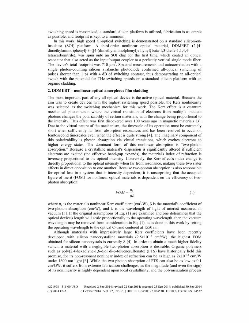
In this work, 0.5 grams of solid DDMEBT were dissolved in 6.5 mL of dichloromethane, resulting in a very dark purple solution. SOI chips were treated with piranha, HF etched, and subjected to vacuum baking at 200 °C and 1mTorr for 2 minutes to remove adsorbed water and ensure a perfectly hydrophobic surface prior to spinning. Two drops of the DDMEBT solution were then dropped onto an SOI chip and immediately spun at 4,000 rpm, as the solvent evaporates in less than one second. Because of the high spin speed, the resulting amorphous film is perfectly uniform and appears perfectly black and mirror-smooth to the eye. Precise ellipsometry of the film was performed with 200 nm to 1800 nm light over 45 to 75 degrees of angular incidence. Owing to DDMEBT's amorphous character, the ellipsometric data was best fit with a Tauc-Lorentz model and was supplemented with six Gaussian oscillators to more accurately model specific absorption peaks. The parameters of the final ellipsometric model are given in Table 1. The chemical structure of DDMEBT is shown in Fig. 1, and the measured n (real index) and k (imaginary index) values for spun-on DDMEBT are in Fig. 2.
Table 1. Material Parameters of Spun-on DDMEBT Ellipsometer Model in WVASE Software
Oscillator Type Amp En C Eg Tauc-Lorentz 19.017 2.0821 0.48545 1.5763
Oscillator Type Amp En Br Gaussian 0.40526 4.1083 0.61403 Gaussian 1.2634 6.2292 0.83819 Gaussian 0.48708 4.8486 1.1995 Gaussian 1.0924 2.4856 0.96558 Gaussian 7.8195 9.0803 1.0246 Gaussian -0.10298 1.1377 0.000121
#221978 - $15.00 USD Received 2 Sep 2014; revised 22 Sep 2014; accepted 23 Sep 2014; published 30 Sep 2014(C) 2014 OSA 6 October 2014 | Vol. 22, No. 20 | DOI:10.1364/OE.22.024530 | OPTICS EXPRESS 24533
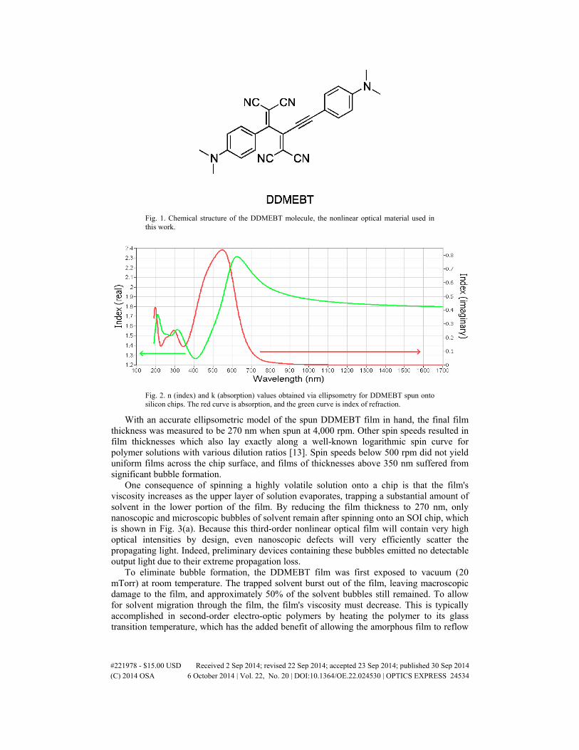
Fig. 1. Chemical structure of the DDMEBT molecule, the nonlinear optical material used in this work.
Fig. 2. n (index) and k (absorption) values obtained via ellipsometry for DDMEBT spun onto silicon chips. The red curve is absorption, and the green curve is index of refraction.
With an accurate ellipsometric model of the spun DDMEBT film in hand, the final film thickness was measured to be 270 nm when spun at 4,000 rpm. Other spin speeds resulted in film thicknesses which also lay exactly along a well-known logarithmic spin curve for polymer solutions with various dilution ratios [13]. Spin speeds below 500 rpm did not yield uniform films across the chip surface, and films of thicknesses above 350 nm suffered from significant bubble formation.
One consequence of spinning a highly volatile solution onto a chip is that the film's viscosity increases as the upper layer of solution evaporates, trapping a substantial amount of solvent in the lower portion of the film. By reducing the film thickness to 270 nm, only nanoscopic and microscopic bubbles of solvent remain after spinning onto an SOI chip, which is shown in Fig. 3(a). Because this third-order nonlinear optical film will contain very high optical intensities by design, even nanoscopic defects will very efficiently scatter the propagating light. Indeed, preliminary devices containing these bubbles emitted no detectable output light due to their extreme propagation loss.
To eliminate bubble formation, the DDMEBT film was first exposed to vacuum (20 mTorr) at room temperature. The trapped solvent burst out of the film, leaving macroscopic damage to the film, and approximately 50% of the solvent bubbles still remained. To allow for solvent migration through the film, the film's viscosity must decrease. This is typically accomplished in second-order electro-optic polymers by heating the polymer to its glass transition temperature, which has the added benefit of allowing the amorphous film to reflow
#221978 - $15.00 USD Received 2 Sep 2014; revised 22 Sep 2014; accepted 23 Sep 2014; published 30 Sep 2014(C) 2014 OSA 6 October 2014 | Vol. 22, No. 20 | DOI:10.1364/OE.22.024530 | OPTICS EXPRESS 24534

and completely fill in nanoscopic holes or trenches in the underlying silicon layer, as well as heal any damage caused by evaporated solvent [14]. The glass transition temperature was coarsely determined by first creating cracks in a DDMEBT film covering a silicon chip by rapidly heating it to 70 °C on a hot plate and then immediately placing it on a metal block at room temperature. Next, the chip was heated incrementally for ten minutes on a hot plate in five degree steps, starting at 30 °C. At each temperature step, the chip was removed from the plate and allowed to cool in close proximity to the hot plate surface to prevent reformation or creation of cracks due to rapid temperature changes. After cooling, the DDMEBT film was observed under an optical microscope. Under these conditions, crack healing was first visually apparent at the 80 °C heating step. The cracks did not disappear entirely until the chip was heated at 90 °C for 10 minutes. Thus, it was concluded that the DDMEBT viscosity was sufficiently lowered to heal microscopic defects at temperatures above 90 °C. Next, DDMEBT spun chips were then vacuum baked at 95 °C at 1 Torr for two hours. Ellipsometry confirmed a 5 nm reduction in film thickness from this process due to sublimation and bubble loss. Although this baking process was successful in driving out the trapped nanoscopic bubbles, the bubbles most likely underwent a consolidation in the low viscosity environment, as the subsequent explosion of the coalesced macrobubbles left behind striated craters several millimeters in diameter, which were too severe to be healed even in a glassy film. To rectify this excessive damage, a two step baking process was developed.
First, the DDMEBT-clad chips were baked at 95 °C and 2 Torr for two hours. Because of the increased pressure, only ~2 nm of material sublimated, which may also be due in part to solvent removal. Second, the chamber pressure was slowly increased to ~650 Torr while holding the temperature constant. The chip was then held in this near-atmospheric state for 2 hours. Afterwards, inspection of the chip under an optical microscope revealed no visible defects of any kind on the chip. In fact, the post-baked surface became so smooth it became extremely challenging to see any lithographic features that lay underneath the film. The visual result is shown in Fig. 3(b).
Fig. 3. Visible dark field microscopy showing (a) DDMEBT as spun onto an SOI chip with pre-etched test patterns and microscopic bubbles in the film and (b) the same chip after a 2-step post bake.
3. Vertical fiber-to-grating coupler
With a 270 nm thick top cladding of DDMEBT film blanketing an SOI chip, the corresponding silicon layer thickness must be determined next. As propagation loss is detrimental to an intensity-dependent all-optical device, TM polarized waveguides were chosen so that the light mode would concentrate along the horizontal interfaces between the silicon dioxide, silicon, and DDMEBT, as the horizontal interfaces (TM) are atomically smooth, while the vertical interfaces (TE) defined through etching processes are substantially rougher and would suffer from larger propagation losses. The thickness of the underlying silicon layer was varied in RSoft FemSIM in order to maximize the TM fundamental mode's
#221978 - $15.00 USD Received 2 Sep 2014; revised 22 Sep 2014; accepted 23 Sep 2014; published 30 Sep 2014(C) 2014 OSA 6 October 2014 | Vol. 22, No. 20 | DOI:10.1364/OE.22.024530 | OPTICS EXPRESS 24535
field intensity in the DDMEBT layer. Ultimately, the field intensity continued to increase monotonically to a 120 nm silicon layer, where the TM mode was no longer guided. As a precaution from encountering the mode cut-off, a silicon thickness of 145 nm was selected. Although 350 nm wide single-mode waveguides were originally designed for this platform, resonator challenges addressed in the next chapter led to the final waveguide being 12 μm wide, which is extremely close to the chip's slab mode.
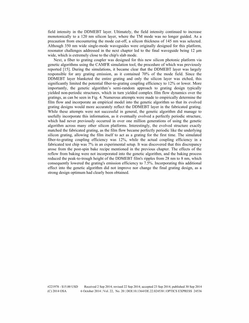
Next, a fiber to grating coupler was designed for this new silicon photonic platform via genetic algorithms using the CAMFR simulation tool, the procedure of which was previously reported [15]. During the simulations, it became clear that the DDMEBT layer was largely responsible for any grating emission, as it contained 70% of the mode field. Since the DDMEBT layer blanketed the entire grating and only the silicon layer was etched, this significantly limited the potential fiber-to-grating coupling efficiency to 12% or lower. More importantly, the genetic algorithm’s semi-random approach to grating design typically yielded non-periodic structures, which in turn yielded complex film flow dynamics over the gratings, as can be seen in Fig. 4. Numerous attempts were made to empirically determine the film flow and incorporate an empirical model into the genetic algorithm so that its evolved grating designs would more accurately reflect the DDMEBT layer in the fabricated grating. While these attempts were not successful in general, the genetic algorithm did manage to usefully incorporate this information, as it eventually evolved a perfectly periodic structure, which had never previously occurred in over one million generations of using the genetic algorithm across many other silicon platforms. Interestingly, the evolved structure exactly matched the fabricated grating, as the film flow became perfectly periodic like the underlying silicon grating, allowing the film itself to act as a grating for the first time. The simulated fiber-to-grating coupling efficiency was 12%, while the actual coupling efficiency in a fabricated test chip was 7% in an experimental setup. It was discovered that this discrepancy arose from the post-spin bake recipe mentioned in the previous chapter. The effects of the reflow from baking were not incorporated into the genetic algorithm, and the baking process reduced the peak-to-trough height of the DDMEBT film's ripples from 28 nm to 8 nm, which consequently lowered the grating's emission efficiency to 7.5%. Incorporating this additional effect into the genetic algorithm did not improve nor change the final grating design, as a strong design optimum had clearly been obtained.
#221978 - $15.00 USD Received 2 Sep 2014; revised 22 Sep 2014; accepted 23 Sep 2014; published 30 Sep 2014(C) 2014 OSA 6 October 2014 | Vol. 22, No. 20 | DOI:10.1364/OE.22.024530 | OPTICS EXPRESS 24536
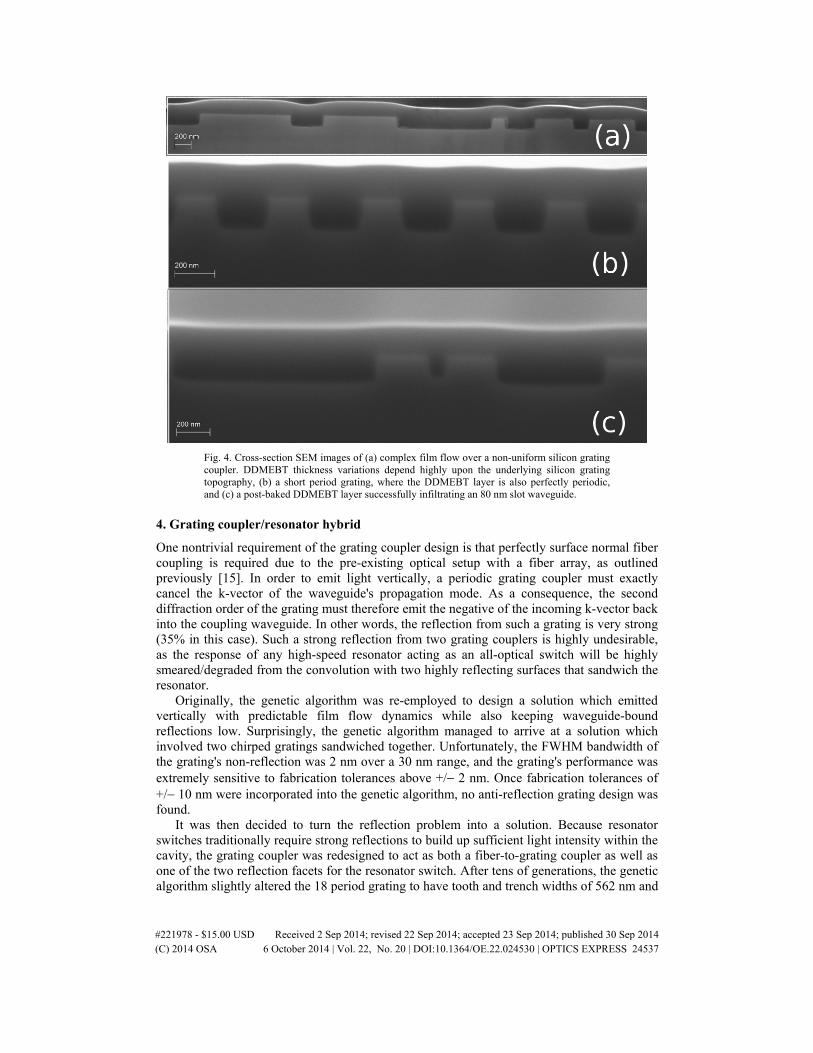
Fig. 4. Cross-section SEM images of (a) complex film flow over a non-uniform silicon grating coupler. DDMEBT thickness variations depend highly upon the underlying silicon grating topography, (b) a short period grating, where the DDMEBT layer is also perfectly periodic, and (c) a post-baked DDMEBT layer successfully infiltrating an 80 nm slot waveguide.
4. Grating coupler/resonator hybrid
One nontrivial requirement of the grating coupler design is that perfectly surface normal fiber coupling is required due to the pre-existing optical setup with a fiber array, as outlined previously [15]. In order to emit light vertically, a periodic grating coupler must exactly cancel the k-vector of the waveguide's propagation mode. As a consequence, the second diffraction order of the grating must therefore emit the negative of the incoming k-vector back into the coupling waveguide. In other words, the reflection from such a grating is very strong (35% in this case). Such a strong reflection from two grating couplers is highly undesirable, as the response of any high-speed resonator acting as an all-optical switch will be highly smeared/degraded from the convolution with two highly reflecting surfaces that sandwich the resonator.
Originally, the genetic algorithm was re-employed to design a solution which emitted vertically with predictable film flow dynamics while also keeping waveguide-bound reflections low. Surprisingly, the genetic algorithm managed to arrive at a solution which involved two chirped gratings sandwiched together. Unfortunately, the FWHM bandwidth of the grating's non-reflection was 2 nm over a 30 nm range, and the grating's performance was extremely sensitive to fabrication tolerances above +/− 2 nm. Once fabrication tolerances of +/− 10 nm were incorporated into the genetic algorithm, no anti-reflection grating design was found.
It was then decided to turn the reflection problem into a solution. Because resonator switches traditionally require strong reflections to build up sufficient light intensity within the cavity, the grating coupler was redesigned to act as both a fiber-to-grating coupler as well as one of the two reflection facets for the resonator switch. After tens of generations, the genetic algorithm slightly altered the 18 period grating to have tooth and trench widths of 562 nm and
#221978 - $15.00 USD Received 2 Sep 2014; revised 22 Sep 2014; accepted 23 Sep 2014; published 30 Sep 2014(C) 2014 OSA 6 October 2014 | Vol. 22, No. 20 | DOI:10.1364/OE.22.024530 | OPTICS EXPRESS 24537
402 nm, respectively. This brought the grating's reflection to 50%, while the coupling efficiency slightly lowered to 11%. Once the post-spin bake effects were included, the coupling efficiency still remained at 7%. In addition, a reflector grating was designed by sweeping all possible tooth and trench widths, resulting in a 65% reflective grating with tooth and trench widths of 240 nm and 252 nm, respectively. Despite being 20 periods long, the reflector grating suffers from low reflectivity due to the low index contrast between the blanketed DDMEBT film and the guided propagation mode, where most of the light guides within the DDMEBT layer.
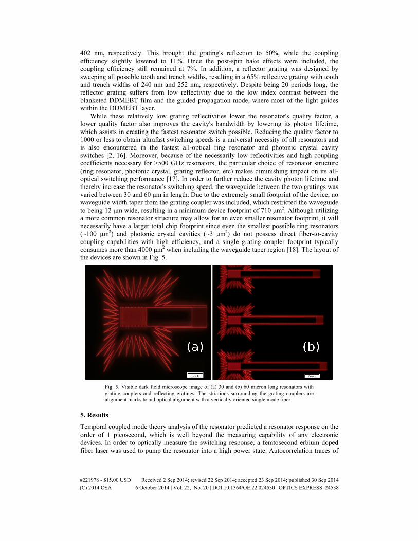
While these relatively low grating reflectivities lower the resonator's quality factor, a lower quality factor also improves the cavity's bandwidth by lowering its photon lifetime, which assists in creating the fastest resonator switch possible. Reducing the quality factor to 1000 or less to obtain ultrafast switching speeds is a universal necessity of all resonators and is also encountered in the fastest all-optical ring resonator and photonic crystal cavity switches [2, 16]. Moreover, because of the necessarily low reflectivities and high coupling coefficients necessary for >500 GHz resonators, the particular choice of resonator structure (ring resonator, photonic crystal, grating reflector, etc) makes diminishing impact on its all-optical switching performance [17]. In order to further reduce the cavity photon lifetime and thereby increase the resonator's switching speed, the waveguide between the two gratings was varied between 30 and 60 μm in length. Due to the extremely small footprint of the device, no waveguide width taper from the grating coupler was included, which restricted the waveguide to being 12 μm wide, resulting in a minimum device footprint of 710 μm2. Although utilizing a more common resonator structure may allow for an even smaller resonator footprint, it will necessarily have a larger total chip footprint since even the smallest possible ring resonators (~100 μm2) and photonic crystal cavities (~3 μm2) do not possess direct fiber-to-cavity coupling capabilities with high efficiency, and a single grating coupler footprint typically consumes more than 4000 μm2 when including the waveguide taper region [18]. The layout of the devices are shown in Fig. 5.
Fig. 5. Visible dark field microscope image of (a) 30 and (b) 60 micron long resonators with grating couplers and reflecting gratings. The striations surrounding the grating couplers are alignment marks to aid optical alignment with a vertically oriented single mode fiber.
5. Results
Temporal coupled mode theory analysis of the resonator predicted a resonator response on the order of 1 picosecond, which is well beyond the measuring capability of any electronic devices. In order to optically measure the switching response, a femtosecond erbium doped fiber laser was used to pump the resonator into a high power state. Autocorrelation traces of
#221978 - $15.00 USD Received 2 Sep 2014; revised 22 Sep 2014; accepted 23 Sep 2014; published 30 Sep 2014(C) 2014 OSA 6 October 2014 | Vol. 22, No. 20 | DOI:10.1364/OE.22.024530 | OPTICS EXPRESS 24538

the output pulse would then give an accurate temporal picture of the switch's impulse response, while spectral analysis of the output from an optical spectrum analyzer (OSA) determines the fidelity of the actual switching process.
Mounting the chip with the device-under-test and the fiber array to optical stages was previously reported [15]. Because a single grating coupler acts as both the input and the output for the setup, a single fiber in the array was then connected to a 1x2 fiber splitter, where the laser input and the output fiber (which connected to either the OSA or the autocorrelator) were connected to the other ends of the splitter. The entire optical setup is shown in Fig. 6(a).
Fig. 6. (a) Diagram of optical setup, where the aligned chip is connected to either a femtosecond pulsed laser and autocorrelator or to a C-band broadband source and optical spectrum analyzer. (b) Schematic of autocorrelator.
Because the DDMEBT top cladding absorbs almost all visible light, alignment marks, as seen in Fig. 5, were lithographically patterned around each grating coupler. Red light from a laser diode was then coupled into the input fiber, allowing the strong scattering from the alignment marks to be clearly visible even to the naked eye (A 20X jeweler's loupe was occasionally used as well). The fiber array was then brought very close to the chip surface while maintaining transverse alignment before switching the laser input to a 1550 nm ASE source and the output fiber to a power detector. Because a single fiber was used for input and output and because the chip is perfectly normal to the fiber, a strong signal of −12 dB system loss was detected whenever the fiber was misaligned away from the on-chip alignment mark. Because the alignment mark and grating coupler both act as efficient anti-reflective surfaces, the signal dropped to −16 dB of system loss when over the alignment mark and −28 dB of total system loss once the fiber was directly 2 μm above the grating coupler. This was 1 dB higher than the coupling losses of the grating coupler and the 1x2 fiber splitter, indicating that chip reflections contributed 20% of the received power. Both the standard 1550 nm laser and femtosecond fiber laser sources were vertically polarized, and both vertically and horizontally oriented grating couplers were fabricated on the same chip. The vertically oriented devices yielded −28 dB system loss, while the horizontally oriented devices yielded −35 dB system loss, indicating that grating coupling into the resonator occurred in the vertically oriented devices and the horizontal ones only outputted a surface normal reflection. This is expected due to the grating coupler only functioning for TM polarizations, as the vertical coupling efficiency for TE polarized light was simulated to be 0.08%. The switching measurements
#221978 - $15.00 USD Received 2 Sep 2014; revised 22 Sep 2014; accepted 23 Sep 2014; published 30 Sep 2014(C) 2014 OSA 6 October 2014 | Vol. 22, No. 20 | DOI:10.1364/OE.22.024530 | OPTICS EXPRESS 24539
discussed below also demonstrate the same polarization sensitivity, further corroborating actual coupling as opposed to measuring spurious reflections.
Once alignment was achieved, it was noted that the total system loss increased very rapidly over a matter of hours to the point where no signal was obtainable 24 hours after mounting the chip. Because DDMEBT has been rigorously tested for its durability, other culprits were investigated [12]. Far-field imaging of reflected red light on the chip's surface revealed real-time dust accumulation. Because the device was TM polarized, large field concentrations at the DDMEBT's surface make the chip's performance extremely sensitive to dust-accumulation in a non-clean environment, as surface defects will very efficiently scatter any propagating light. By surrounding the optical stages with plastic tents, HEPA grade air filters, and wearing cleanroom suits during optical alignment, a marked improvement was noticed, where only 5 dB of additional system loss was encountered after leaving the chip mounted for 24 hours. Given the optical lab's relative humidity of 70%, it was strongly suspected that excessive humidity could also be absorbed by the DDMEBT layer. Furthermore, after being exposed to solvent, DDMEBT becomes sensitive to visible light. Thus, all subsequent chips were encased in clear, dark red plastic holders that were then immersed in silica gel. All subsequent chips experienced no measurable degradation when stored in this environment next to the optical stages, and although these precautions could not be tested while the chip was optically mounted, the results strongly hint at the potential vulnerabilities of spun-on DDMEBT.
The femtosecond laser had an average power of 17 mW and a repetition rate of 20 MHz. The output pulses were expected to be ~1 ps in duration. Taking into account the −29 dB system loss for the output pulse, the average power to be detected was 21μW and the outgoing peak power is 1 W, which requires a PavgPpeak sensitivity of at least 2x10⁻⁵ W2 to be detected. Such a low signal is below the sensitivity of routine autocorrelators that use BBO nonlinear crystal to perform an autocorrelation via second-harmonic generation. A simpler, more sensitive method of performing autocorrelation on weak telecommunications pulses was developed in 2002 by performing the autocorrelation function with two-photon absorption in a single photon counting silicon avalanche photodiode, where the sensitivity was measured at 1.5x10⁻⁹ W2 and could potentially be even lower based on the reported noise floor [19]. A similar intensity-based Michelson-interferometer autocorrelator was constructed using a fiber-to-free-space collimator, a 1550 nm pellicle beamsplitter, two flat silver mirrors for each beam arm, where one is mounted on a longitudinally oriented micrometer to vary one of the beams' path lengths, a best form BK7 lens, and a single photon counting silicon avalanche photodiode with an electron quenching circuit and heat sink. A schematic of the autocorrelator setup is shown in Fig. 6(b).
First, the femtosecond laser was directly connected to the autocorrelator's fiber collimator via a one meter polarization-maintaining single mode fiber. Because the fiber's distance was slightly longer than twice the length of the polarization maintaining fiber array used to couple to the chip, it was presumed that the pulse dispersion would be nearly identical in both cases and would act as an acceptable proxy for measuring the input pulse length to the device-under-test. One of the autocorrelator mirror distances was manually tuned, and 1,000 power measurements were recorded from the single photon counter at each mirror location. The entire measured pulse from the femtosecond laser appeared above and then disappeared below the linear signal floor after two 1/10th knob turns. This corresponded to a path length change of 127 μm, which equates to a pulse width of 423 femtoseconds. The quadratic nature of intensity based autocorrelation underestimates pulse-widths, but since the measured pulse width spanned beyond its FWHM, the measured result was accepted as the general pulse width that would enter the device-under-test.
Next, the femtosecond pulse laser was reconnected to the 1x2 fiber splitter as an input to the chip, and autocorrelation traces were performed as stated above on the output pulses from the optical resonator devices. The results are shown below in Fig. 7. Because reflections were
#221978 - $15.00 USD Received 2 Sep 2014; revised 22 Sep 2014; accepted 23 Sep 2014; published 30 Sep 2014(C) 2014 OSA 6 October 2014 | Vol. 22, No. 20 | DOI:10.1364/OE.22.024530 | OPTICS EXPRESS 24540

measured from the chip surface, it is expected that the reflected pulse shall create a peak in the trace that is sharper and narrower than the rest of the pulse since it does not encounter the resonator. Such a phenomenon is visible on both traces.
Fig. 7. Autocorrelation traces (black) and coupled mode theory simulations (blue) of (a) the 30 μm long optical resonator, and (b) the 60 μm long optical resonator. The largest average power values obtained over all trace sweeps are given at each data point in order to best show the autocorrelation envelope. Each data point contains 1,000 power samples.
To evaluate the validity of the pulse traces, coupled mode theory simulations were performed for the resonators, which included the grating coupler efficiency as the out-coupling mechanism. The procedure of accurately modeling strongly out-coupled resonator systems in coupled mode theory has been adequately addressed in the work of others [20, 21]. Because autocorrelation underestimates a measured pulse width, it is expected that the trace should be approximately 30% narrower in time than the actual pulse width for a Gaussian pulse. By comparing the autocorrelation pulse shape with the pulses obtained from coupled mode theory for each resonator, it can be seen that both resonators have the expected impulse response. The FWHM impulse response of the 60 μm long optical resonator from coupled mode theory is 1.4 ps, while the 30 μm long optical resonator's FWHM is 600 fs, indicating a response time sufficient to generate ~1 THz data signals. As mentioned in section 2, the transparent (off-resonant) Kerr effect of a material has a response time on the order of femtoseconds. Because the resonator's measured temporal response is slower by two orders of magnitude, the device's switching speed is limited by the grating resonator and not the material itself. This limitation in speed allows for a dramatically reduced interaction length in order to enable densely integrated all-optical devices.
#221978 - $15.00 USD Received 2 Sep 2014; revised 22 Sep 2014; accepted 23 Sep 2014; published 30 Sep 2014(C) 2014 OSA 6 October 2014 | Vol. 22, No. 20 | DOI:10.1364/OE.22.024530 | OPTICS EXPRESS 24541

Light from the femtosecond fiber laser was then coupled to the DDMEBT-clad silicon grating/resonator device, and the output spectra for varying peak powers were measured, as seen in Fig. 8(a). The resonance peaks blueshift by nearly 4 nm when the laser fluence is reduced by a mere 8%, which corresponds to a nonlinear coefficient of approximately −1.3x10⁻¹¹ cm2/W. Two-photon absorption in the silicon layer was originally suspected, as the generated free carrier dispersion reduces the silicon's index of refraction, potentially blueshifting a resonance. A new chip was then fabricated where the silicon guiding layer was etched away, leaving only a planar DDMEBT resonator surrounded by two silicon gratings. The silicon thickness in the gratings was also increased to 220 nm to increase the grating index contrast, which allowed over 90% of the incident power to be reflected/emitted in only six periods for both gratings, thereby minimizing the amount of silicon (and two-photon absorption) exposure. The spectral result of the identical measurement is shown in Fig. 8(b).
Fig. 8. Spectral output of DDMEBT resonators (a) with an underlying silicon waveguide and (b) without underlying silicon exposed to a 20 MHz repetition rate femtosecond pulse laser at various input powers. A very strong blueshift is observed in both devices as input fluence increases. All spectral curves are normalized to the femtosecond fiber laser output at maximum input current.
Since the amount of blueshift was virtually identical to the previous chip, another negative index nonlinear mechanism must be at work. Indeed, most thin molecular films exhibit fairly strong negative thermo-optic coefficients on the order of 10 −11 cm2/W, which would likely
#221978 - $15.00 USD Received 2 Sep 2014; revised 22 Sep 2014; accepted 23 Sep 2014; published 30 Sep 2014(C) 2014 OSA 6 October 2014 | Vol. 22, No. 20 | DOI:10.1364/OE.22.024530 | OPTICS EXPRESS 24542

manifest itself when probed with a 20 MHz repetition rate pulsed laser, as the thermal recovery time of a thin polymer is on the order of microseconds [22]. To eliminate thermal accumulation effects, the DDMEBT planar resonator chip was instead coupled to a 5 kHz repetition rate femtosecond laser. The incident power was then tuned from the noise floor to the highest sustainable peak power within the single mode fiber before soliton and super-continuum generation became evident in the fiber output. The resulting spectra is shown in Fig. 9. First, the disappearance of the strong blueshift when using a low repetition rate laser confirms the previously measured switching effects were thermo-optic in nature. Second, the corresponding redshift of 4 nm in the resonance spectra when experiencing 1 kW peak power indicates a positive nonlinear coefficient of no less than 10−13 cm2/W, which matches the previously measured Kerr coefficient of DDMEBT [11]. At these powers, the on/off ratio of the ultrafast Kerr-switching mechanism reaches a 4 dB contrast.
The amount of mitigating blueshift experienced due to the silicon gratings is calculated with a two-photon absorption rate of 0.79 cm/GW in crystalline silicon under 1550 nm pulsed light [23]. Because any incoming and/or propagating light encounters less than 2 μm of silicon material in each grating before experiencing out-coupling, all of the remaining silicon within the final device only absorbs 0.25% of the light through two-photon absorption. By calculating the free-carrier plasma dispersion effect from the number of carriers generated by two-photon absorption as outlined in [24], a negative index change with a resulting resonance blueshift of 0.6 nm from the silicon gratings is obtained. This result indicates that the true Kerr coefficient of the DDMEBT resonator is approximately 12% higher than is directly calculated from the spectral redshift of 4 nm seen in Fig. 9.
Fig. 9. Spectra at various coupled peak powers from a 5 kHz femtosecond laser into a 43 μm long DDMEBT slab resonator/coupler hybrid with underlying silicon removed in the resonator region.
6. Conclusion
DDMEBT, a third-order nonlinear optical molecular compound with a very high figure of merit, was successfully spun onto silicon chips for the first time from a dichloromethane solution. A two-step post-spin bake removed all bubbles from the film and allowed for
#221978 - $15.00 USD Received 2 Sep 2014; revised 22 Sep 2014; accepted 23 Sep 2014; published 30 Sep 2014(C) 2014 OSA 6 October 2014 | Vol. 22, No. 20 | DOI:10.1364/OE.22.024530 | OPTICS EXPRESS 24543

reflow, completely filling features as small as 80 nm wide trenches. A novel, compact (< 720 μm2) nonlinear resonator was designed, fabricated, and tested, where one of the two silicon-based reflector gratings also acted as an input/output coupler to a surface normal single mode fiber. Using a femtosecond fiber laser and an extremely sensitive single photon counting silicon avalanche photodiode-based autocorrelator, the measured impulse responses of the resonators ranged from 0.6 ps to 1.4 ps for 30 μm and 60 μm long resonators, respectively. By varying the input power coupled from a 20 MHz repetition rate femtosecond laser into the nonlinear resonator, strong thermo-optic switching on the order of −1.3x10⁻¹¹ cm2/W was obtained from spectral measurements. Coupling pulses from a 5 kHz femtosecond laser into the resonator yielded ultrafast Kerr-based nonlinear resonance redshifts as large as 4 nm of bandwidth with 4 dB of switching contrast. Due to both the nonlinear material and resonators' ultrafast temporal response, the device is potentially capable of switching at ~1 THz on a single carrier frequency, provided that the input powers are the highest that a single mode fiber can reliably deliver.
Acknowledgments
Material preparation at ETH Zurich was funded by the ERC Advanced Grant No. 246637 (“OPTELOMAC”). Financial support from the Cullen Trust For Higher Education is gratefully acknowledged. Ivan Biaggio's timely and insightful feedback on this project is highly appreciated. Usage of the continually improving IPKISS project has saved immeasurable amounts of time and is acknowledged.
#221978 - $15.00 USD Received 2 Sep 2014; revised 22 Sep 2014; accepted 23 Sep 2014; published 30 Sep 2014(C) 2014 OSA 6 October 2014 | Vol. 22, No. 20 | DOI:10.1364/OE.22.024530 | OPTICS EXPRESS 24544