all-optical header processing based on nonlinear gain and
TRANSCRIPT

All-optical header processing based on nonlinear gain andindex dynamics in semiconductor optical amplifiersCitation for published version (APA):Calabretta, N. (2004). All-optical header processing based on nonlinear gain and index dynamics insemiconductor optical amplifiers. Technische Universiteit Eindhoven. https://doi.org/10.6100/IR573184
DOI:10.6100/IR573184
Document status and date:Published: 01/01/2004
Document Version:Publisher’s PDF, also known as Version of Record (includes final page, issue and volume numbers)
Please check the document version of this publication:
• A submitted manuscript is the version of the article upon submission and before peer-review. There can beimportant differences between the submitted version and the official published version of record. Peopleinterested in the research are advised to contact the author for the final version of the publication, or visit theDOI to the publisher's website.• The final author version and the galley proof are versions of the publication after peer review.• The final published version features the final layout of the paper including the volume, issue and pagenumbers.Link to publication
General rightsCopyright and moral rights for the publications made accessible in the public portal are retained by the authors and/or other copyright ownersand it is a condition of accessing publications that users recognise and abide by the legal requirements associated with these rights.
• Users may download and print one copy of any publication from the public portal for the purpose of private study or research. • You may not further distribute the material or use it for any profit-making activity or commercial gain • You may freely distribute the URL identifying the publication in the public portal.
If the publication is distributed under the terms of Article 25fa of the Dutch Copyright Act, indicated by the “Taverne” license above, pleasefollow below link for the End User Agreement:www.tue.nl/taverne
Take down policyIf you believe that this document breaches copyright please contact us at:[email protected] details and we will investigate your claim.
Download date: 19. Dec. 2021

ALL-OPTICAL HEADER PROCESSING
BASED ON NONLINEAR GAIN AND INDEX DYNAMICS IN SEMICONDUCTOR
OPTICAL AMPLIFIERS
PROEFSCHRIFT
ter verkrijging van de graad van doctor aan de Technische Universiteit Eindhoven, op gezag van de Rector Magnificus, prof.dr. R.A. van Santen,
voor een commissie aangewezen door het College voor Promoties in het openbaar te verdedigen
op dinsdag 13 april 2004 om 16.00 uur
door
Nicola Calabretta
geboren te Catanzaro, Italië

Dit proefschrift is goedgekeurd door de promotoren: prof.ir. G.D. Khoe en prof.dr. D. Lenstra Copromotor: dr. H.J.S. Dorren The work described in this thesis was performed in the Faculty of Electrical Engineering of the Eindhoven University of Technology and was financially supported by Netherlands Organization for Scientific Research (NWO) through the “NRC Photonics” grant. CIP-DATA LIBRARY TECHNISCHE UNIVERSITEIT EINDHOVEN Calabretta, Nicola All-optical header processing based on nonlinear gain and index dynamics in semiconductor optical amplifiers / by Nicola Calabretta. – Eindhoven: Technische Universiteit Eindhoven, 2004. Proefschrift. – ISBN 90-386-1543-4 NUR 959 Trefw.: optische patroonherkenning / optische signaalverwerking / nietlineaire optica / halfgeleiderversterkers / optische telecommunicatiesystemen / computernetwerken ; packet switching. Subject headings: optical information processing / optical logic / nonlinear optics / semiconductor optical amplifiers / packet switching. Copyright © 2004 by Nicola Calabretta All rights reserved. No part of this publication may be reproduced, stored in a retrieval system, or transmitted in any form or by any means without the prior written consent of the author. Typeset using Microsoft Word, printed in The Netherlands.

Summary
This thesis is devoted to all optical header recognition. All-optical header recognizers
play an important role in futuristic all-optical packet switches. In the literature several
approaches for all-optical header recognition have been discussed, but in this thesis, we
focus on all-optical header recognition based on nonlinear gain and index dynamics in
semiconductor optical amplifiers.
After a general introduction on the topic, in Chapter 2 an all-optical packet switch
concept is discussed. This packet switch contains an optical header processor that is
operated by employing two-pulse correlation principles in a semiconductor optical
(laser) amplifier that is placed in an optical loop mirror (SLALOM). The header
processor used in the packet switch presented in Chapter 2 can only recognize 1 specific
header pattern. In Chapter 3 of this thesis, it is shown how header recognition concepts
that are based on two-pulse correlation principles can be extended to recognize a larger
amount of packet headers.
Also the packet switch presented in Chapter 2 contains an optical threshold function.
This function was necessary since the header recognizer in the packet switch could only
suppress the packet payload. Therefore in Chapter 4 and all-optical header pre-
processor is discussed that solves this issue.

SUMMARY
vi
In Chapter 5 of this thesis all-optical header processing is discussed employing self-
induced nonlinear polarisation rotation in a semiconductor optical amplifier. The
advantage of employing header processing and header pre-processing employing
nonlinear polarisation rotation is that the optical powers to be injected in the header
processing system could be drastically reduced.
Finally, In Chapter 6, we show concepts for all-optical header recognition
employing terahertz optical asymmetric demultiplexers (TOADs). The advantage of
employing TOADs instead of SLALOMs is that header recognizers employing TOADs
can be made so compact so that the system allows photonic integration. In Chapter 6, a
concept is presented in which TOADs are employed for optical header recognition. In
contrast to other optical header recognition concepts employing TOADs, the one
presented in Chapter 6 of this thesis does not require optical clock recovery.

To Suzanne


Contents
1 Introduction 1
1.1 Why all-optical packet switching?....................................................................1
1.2 All-optical packet switch: state-of-the-art ........................................................4
1.3 1x2 All-optical packet switch............................................................................9
1.4 Scope of the thesis ...........................................................................................12
1.5 Structure of the thesis......................................................................................14
2 All-optical packet switch 17
2.1 Introduction .....................................................................................................17
2.2 All-optical header processing..........................................................................19
2.3 All-optical flip-flop memory...........................................................................22
2.4 All-optical packet switch: experiments...........................................................25
2.5 Conclusions......................................................................................................29
3 Multi-output all-optical header processor 33
3.1 Introduction......................................................................................................33
3.2 Multi-output all-optical header processor.......................................................34
3.3 Experiments .....................................................................................................37
3.4 Conclusions......................................................................................................40
4 All-optical header processor assisted by an all-optical header pre-processor 43
4.1 Introduction......................................................................................................43
4.2 All-optical header pre-processor .....................................................................45
4.3 Experiments .....................................................................................................47
4.4 All-optical header processing system .............................................................50

CONTENTS
viii
4.5 All-optical header processing system: experiments .......................................53
4.6 Conclusions......................................................................................................55
5 Optical signal processing based on self-induced nonlinear polarization rotation
in a semiconductor optical amplifier 59
5.1 Introduction......................................................................................................59
5.2 Self-polarization rotation.................................................................................61
5.3 Self-induced nonlinear polarization switch: experiments ..............................63
5.4 All-optical header processor............................................................................69
5.4.1 All-optical header processor: experiments ......................................73
5.5 All-optical header pre-processor .....................................................................76
5.6 All-optical seed pulse generator......................................................................79
5.6.1 All-optical self-synchronizer: experiments .....................................80
5.7 All-optical arbiter ............................................................................................83
5.7.1 All-optical arbiter: experiments .......................................................84
5.8 Conclusions......................................................................................................87
6 Ultrafast asynchronous multi-output all-optical header processor 91
6.1 Introduction......................................................................................................91
6.2 Ultrafast all-optical header processor .............................................................93
6.3 Experiments .....................................................................................................98
6.4 Conclusions....................................................................................................100
7 Conclusions 103
A Model for nonlinear polarization rotation in a semiconductor optical 109
Amplifier
B Characterization of the semiconductor optical amplifier 117
C Description of the hexadecimal notation and Manchester code 125

CONTENTS
ix
References 129
List of abbreviations 135
List of publications 137
Summary in Italian 141
Acknowledgments 143
Curriculum vitae 145

Chapter 1
Introduction 1.1 Why all-optical packet switching?
In the last ten years, we have been witness of one of the most powerful
telecommunication revolutions that has radically changed our habits, the Internet. A
multitude of telecommunication services based on the Internet has captured many users
and has pushed the telecom industry to invest in higher capacity systems. Internet
demand together with WDM technology has driven a tremendous growth to the optical
fiber infrastructure. Today’s optical networks are built on transponder based point-to-
point WDM transmission systems with a speed of 10-40 Gbit/s. In Internet, data are
transmitted in blocks called data packets; each data packet includes a header that
specifies its destination. Optical circuit switches, mostly based on SDH/SONET
technology [Garnot, O’Mahony, Sonet], interconnect the point-to-point WDM
transmission system as well as route the data packets and monitor the optical networks.
Optical packet switches, read the header, interpret the address, and route the data out a
suitable port. A packet generally passes through a large number of packet switches on
its way to its destination.

INTRODUCTION
2
A number of studies show that the Internet traffic on the networks is still doubling
every 8-12 months [Bourouha, Rau]. Moreover, new services such as video-based on IP
networks in education, medical, entertainment and shopping will increase the demand
for more bandwidth [Akiba]. Thus, optical networks operating at higher bit rate than the
today’s networks will be required. However, while ultrafast point-to-point WDM
transmission systems have been demonstrated in laboratory with a speed of tens of
Tbit/s [Bakhshi, Charlet], high-speed optical packet switches operating at the same line-
rate of the transmission system should be realized to effectively distribute high bit rate
data packets to the users through optical networks.
The current generation of optical packet switches is based on electronic circuit
switching technology that makes connections between networks terminals. Historically,
circuit switching evolved from the voice telephone network, which original purpose
was to form an electrical circuit connecting two telephones. In the telephone networks,
wires carry electrical analog voice signals between individual phones and a point in the
network where the calls are digitized and time-division multiplexed (TDM) into data
streams. Today’s optical packet switches should handle digital packets assembled by
multiplexing many digitalized voice circuits and IP data, but the principle is similar; the
switches form an optical connection between two devices or points. In these opaque
networks, the optical path between the end-users is interrupted at intermediate nodes by
optical-electrical-optical (OEO) conversions. As well as being expensive, these OEO
conversions introduce line-rate dependencies, which make it difficult for carriers to
scale the infrastructure with bandwidth demand. Thus, the speed of the today’s optical
packet switches is fundamentally mismatched with the line-rate of the optical
transmission system.

CHAPTER 1
3
A possible scenario for futuristic optical networks is one that implements all-
optical packet switching technology. In such a case, the data packets are kept in the
optical domain. The switching is based on routing information contained in the header
section of the packets. In today’s electrical packet switched networks, the common way
of sending the routing information is in the header bits that are located near the front of
the data packet. One can envision that futuristic all-optically packet switched networks
will maintain this convention and require optical recognition of header bits in order to
route a packet. Thus, transparent optical networks based on all-optical packet switching
can take advantage of photonic parallel processing to route bands of optical channels at
speeds that are not achievable through electronic processing.
An all-optical packet switch that acts as an optical router should perform several
functions. Firstly, optical packet switches should be able to all-optically read the header
of each packet (header processing). Secondly, the processed header information should
be stored in an optical memory (optical flip-flop memory). Finally, the processed
header information should drive the optical switches that routes the packet to the proper
destination perhaps with a revised header (optical switching). This thesis will deal with
realizing an all-optical header processing system.
In the next section, an overview of the state-of the art of the all-optical packet
switching and the techniques to recognize the header patterns are presented. From this
overview, it turns out that two fundamental functions should be developed to all-
optically route optical packets: All-optical header processing and all-optical flip-flop
memories. These two functions will be discussed in this thesis. In Section 1.3, a novel
1x2 all-optical packet switch that employs all-optical header processor to route the
optical packets is briefly introduced. A crucial function to extend the 1x2 all-optical

INTRODUCTION
4
packet switch to 1xN all-optical packet switch is a header processor that distinguishes a
large number of header patterns. Moreover, low power asynchronous, and high speed
operation as well as photonic integration are important features of the header processor
to make a 1xN all-optical packet switch feasible. In Section 1.4, such an all-optical
header processing is stated as the scope of the thesis. Finally, the structure of the thesis
is presented and the major results developed in this thesis are summarized.
1.2 All-optical packet switch: state-of-the-art
Several research groups have used the architecture of the all-optical packet
switch cross-connect as shown in Figure 1.1 [Keops, Murata]. It follows from Figure
1.1 that in the switching fabric three important steps take place: synchronization of the
packets (including pre-amplification and regeneration of the incoming data packet),
buffering that solves the contention resolution between packets at the given moment,
and the third step is the switching block that routes the packets to the defined output
ports based on the header information.
Figure 1.1: Generic node structure for all-optically packet switched cross-connects.
Buffer
λ1λ1...λn
λ n
Port 1
Synch λ1...λn
λ1...λnBuffer
MUX Synchronization Buffering Switching
Synch
λ1
λn
DEMUX
Port N
Port 1
Port Nλ1...λn
CHAPTER 1
5
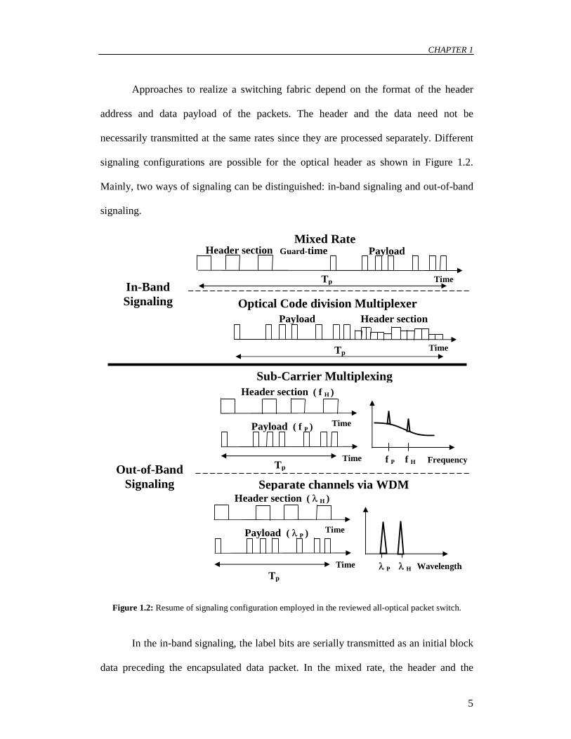
Approaches to realize a switching fabric depend on the format of the header
address and data payload of the packets. The header and the data need not be
necessarily transmitted at the same rates since they are processed separately. Different
signaling configurations are possible for the optical header as shown in Figure 1.2.
Mainly, two ways of signaling can be distinguished: in-band signaling and out-of-band
signaling.
Figure 1.2: Resume of signaling configuration employed in the reviewed all-optical packet switch.
In the in-band signaling, the label bits are serially transmitted as an initial block
data preceding the encapsulated data packet. In the mixed rate, the header and the
Out-of-Band Signaling
Tp
Sub-Carrier Multiplexing
Header section ( f H )
Payload ( f P )
f P f H Frequency
Time
Time
Header section ( λ H )
Payload ( λ P )
λ P λ H Wavelength
Time
Time
Separate channels via WDM
Tp
In-Band Signaling
Mixed Rate
Guard-time Header section Payload
Time Tp
Optical Code division Multiplexer Payload
Header section
Time Tp

INTRODUCTION
6
payload are transmitted at different data rates (see Figure 1.2); the header data has a
lower data rate than the payload. An interval called the guard time separates the header
address from the data payload, giving time for the system to start processing the header
information before dealing with the encapsulated data. Moreover, a tail section could be
attached at the end of the packets. The tail section can be used in systems that employ
packets with variable length.
In the Optical Code Division Multiplexer (OCDM), see Figure 1.2, the in-band
signaling is a time-space pre-processed CDMA information transmitted in the same
optical channel.
In the out-of-band signaling the header information is transmitted in parallel
with the encapsulated packet, either via Sub-Carrier Multiplexing (SCM) on the same
optical channel as the data, or on a separate optical channel using wavelength-division
multiplexing (WDM), as shown in Figure 1.2. Each of the reported possibilities
depends on the technique employed to recognize the header information.
During the past few years a number of switching fabric strategies towards
optically packet switching has been conducted. Glesk et al. firstly demonstrated all-
optical address recognition and self-routing of photonic packets in a 250 Gbit/s packet-
switched network [Glesk2]. They employed a Terahertz Optical Asymmetric
Demultiplexers (TOADs) as header recognizer. Cotter et al. presented experimental
results from a 100 Gbit/s self-routing packet demonstration and from a synchronous
TDMA test bed [Cotter1]. Both of the reported experiments employed in-band signaling
and a specially designed address code is needed to retrieve the header address from the
data payload. Although both header recognizing methods operate at low power and
allow photonic integration, they require a form of optical synchronization that
CHAPTER 1
7
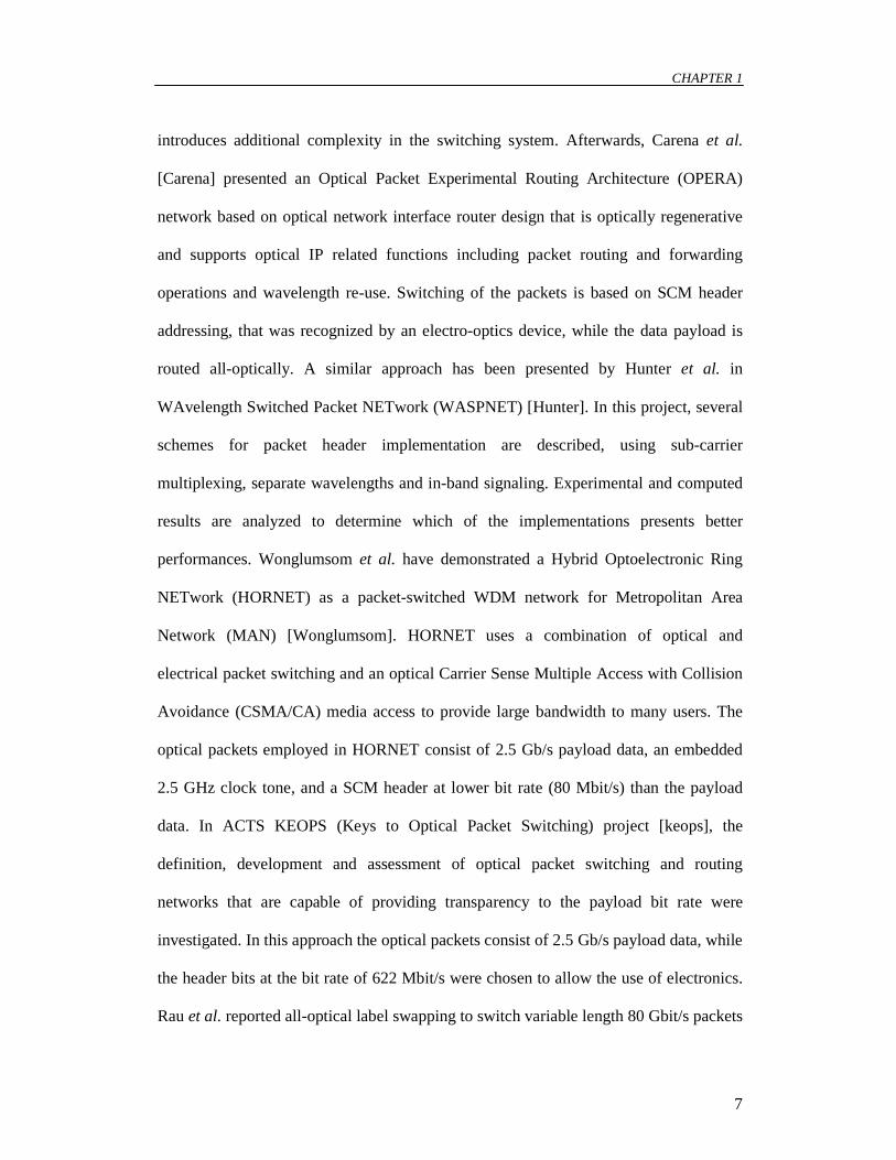
introduces additional complexity in the switching system. Afterwards, Carena et al.
[Carena] presented an Optical Packet Experimental Routing Architecture (OPERA)
network based on optical network interface router design that is optically regenerative
and supports optical IP related functions including packet routing and forwarding
operations and wavelength re-use. Switching of the packets is based on SCM header
addressing, that was recognized by an electro-optics device, while the data payload is
routed all-optically. A similar approach has been presented by Hunter et al. in
WAvelength Switched Packet NETwork (WASPNET) [Hunter]. In this project, several
schemes for packet header implementation are described, using sub-carrier
multiplexing, separate wavelengths and in-band signaling. Experimental and computed
results are analyzed to determine which of the implementations presents better
performances. Wonglumsom et al. have demonstrated a Hybrid Optoelectronic Ring
NETwork (HORNET) as a packet-switched WDM network for Metropolitan Area
Network (MAN) [Wonglumsom]. HORNET uses a combination of optical and
electrical packet switching and an optical Carrier Sense Multiple Access with Collision
Avoidance (CSMA/CA) media access to provide large bandwidth to many users. The
optical packets employed in HORNET consist of 2.5 Gb/s payload data, an embedded
2.5 GHz clock tone, and a SCM header at lower bit rate (80 Mbit/s) than the payload
data. In ACTS KEOPS (Keys to Optical Packet Switching) project [keops], the
definition, development and assessment of optical packet switching and routing
networks that are capable of providing transparency to the payload bit rate were
investigated. In this approach the optical packets consist of 2.5 Gb/s payload data, while
the header bits at the bit rate of 622 Mbit/s were chosen to allow the use of electronics.
Rau et al. reported all-optical label swapping to switch variable length 80 Gbit/s packets

INTRODUCTION
8
with 10 Gbit/s headers over two hops [Rau]. Although the recognition of the header
information has been carried out partly in electronics, this demonstrates that optical
packet switching technology can operate at much higher bit rate than the electronic
circuit switching technology. Moreover, Murata et al. developed an all-optical header
processor without the conventional opto-to-electronic conversion [Murata]. The address
information was expressed in a code used in OCDMA technology. Passive optical
correlators were employed for recognizing the address information. When the optical
correlator recognizes the address, a correlation pulse is formed at the optical correlator
output. This correlation pulse can be used to control the switching block. Although the
header processor allows photonic integration, the number of addresses that this header
processor can recognize could be limited by the phase noise built up along the
transmission between two nodes. Moreover, the optical switching block is still
controlled by using OEO conversion.
All these approaches have shown that developments of ultrafast all-optical
switches for ultra high speed routing based on wavelength routing switching of payload
up 160 Gbit/s and beyond [Patel, Sokoloff, Schreieck] give to all-optical packet switch
effectively advantages over electronics. However, the leak of an all-optical header
processor that all-optically controls a wavelength routing switch based all-optical
packet switch has limited the processing speed of the header information to a few
Gbit/s.
In the following section, a proof-of-principle of a 1 x 2 all-optical packet switch
concept that employs all-optical header processor to route all-optically the packet is
presented [Hill1, Dorren1]. The all-optical header processor is a low power device,
asynchronous and bit-rate transparent.

CHAPTER 1
9
1.3 1x2 All-optical packet switch An optical packet switch that operates in an optical packet switched cross-connect with
a node structure as schematically presented in Figure 1.1 was demonstrated in [Hill1,
Dorren1]. The function of the packet switch is to route the packet to the proper output
port. The 1x2 all-optical packet switch is schematically shown in Figure 1.3 [Hill1,
Dorren1]. The packet switch is based on wavelength routing principles. All the
processing of the header information is carried out in the optical domain. The all-optical
packet switch is made out of three functional blocks: an all-optical header processing
block, an all-optical flip-flop memory block, and a wavelength conversion block.
Figure 1.3: System concept for 1×2 all-optical packet switch.
The packets employed have a fixed duration and consist of an optical header and optical
payload (shown in Figure 1.3). Between the header and the payload, there is some
guard time. The header contains the routing information of the packet while the payload
contains the information content. Both the header and the payload consist of amplitude
modulated data bits. While the header data is Non-Return to Zero (NRZ) encoded, the
payload data is Manchester encoded. Moreover, the header data has a lower bit rate than
Delay line W
avel
engt
h de
mux
wavelength converter
Optical Flip-Flop
State 1 State 2
Output 1
Output 2
Header Processor
Head er 2
Header Pattern 2.5 Gbit/s NRZ
Payload: 10 Gb/s Manchester encoded
Packet format: Guard Time
Tail

INTRODUCTION
10
the payload. When an optical packet arrives at the optical packet switch, the optical
power of the packet is split into two parts. Half of the optical power of the packet is
delayed and injected into a wavelength converter. Some delay is required to compensate
for the time taken to carry out the header processing functions.
The principle that is used for wavelength conversion is cross-gain modulation
[Durhuus]. Wavelength conversion by using cross-gain modulation can be obtained in a
SOA by simultaneously injecting a continuous wave signal and a modulated data signal
into the SOA. By using a demultiplexer, the desired wavelength channels can be
separated spatially. Wavelength conversion by using cross-gain modulation leads to an
inverted data signal. By using a combination of cross-gain modulation and cross-phase
modulation through interferometric wavelength converters a non-inverted signal can be
obtained [Durhuus]. In order to use wavelength conversion principles to route optical
packets all-optically, the binary optical header pattern must be translated into a
continuous wave signal of the desired wavelength. Therefore, firstly the header block
has to recognize the header bits. If a packet header is recognized, the header processor
creates a correlation pulse that is converted into the continuous wave by an optical flip-
flop memory. The optical flip-flop memory’s output is fed into the wavelength
converter to convert the packet into the desired wavelength.
The header processor employed in the packet switch is based on the two-pulse
correlation principles in a Semiconductor Laser Amplifier in Loop Optical Mirror
(SLALOM) configuration [Srivatsa, Eiselt]. The advantage of this method is that it is
does not require optical clock recovery, which reduces the complexity of the header
recognition system. Moreover, the method can be used to recognize low power optical
headers. On the other hand, header recognition by using two-pulse correlation in a

CHAPTER 1
11
SLALOM structure only works for well-chosen header patterns, and Manchester
encoding of the payload is necessary to guarantee that the header pattern is not repeated
in the packet’s payload. In [Calabretta1] it is discussed how a multiple output low
power optical header processor could be realized. Finally, the header processor is bit
rate transparent.
The second function that is needed in order to realize all-optical switching of data
packets is an all-optical flip-flop memory function. In [Kawaguchi] a review is
presented on available technology with respect to optical flip-flop memories. We use in
our optical packet switch an all-optical flip-flop concept that is based on the bi-stable
operation of two coupled laser diodes. The operation principle of the optical flip-flop is
described in [Hill2, Hill3]. The optical flip-flop that we use in this paper has a number
of advantages. Firstly, it can provide high contrast ratios between the states. Moreover,
there is no different mechanism for the set and reset operation. Furthermore, the
wavelength range of the input light and the output wavelength can be large and the flip-
flop has controllable and predictable switching thresholds. Finally, the flip-flop
operation does not rely on second order laser effects and is not tied to a specific
structure or technology.
In [Hill1, Dorren1] a 1×2 all-optical packet switch was realized that uses a
SLALOM structure as a header processor and an optical flip-flop memory based on
coupled laser diodes to store the processed header information. The packet switch
concept is bit-rate transparent for both the header and the payload. Moreover, the packet
switch requires only a limited amount of active components, and it does not require
optical clock recovery or external control. The header processor employed in the 1x2
all-optical packet switch can recognize between well-designed packets. In principle, the

INTRODUCTION
12
concept of the 1x2 all-optical packet switch can be generalized to a 1xN all-optical
packet. Crucial is then to extend the header processing technique of [Hill1] to form a
header processor that has a large number of output ports.
1.4 Scope of the thesis
The purpose of this thesis is to realize an all-optical header processing that can
be used in all-optical packet switches. The header processing system must be able to
distinguish between a large number of header patterns, operate at low power and allow
photonic integration. These features of the header processor are essential in developing
a scalable and packet-level switching all-optical packet switch. These issues associated
with the header processor will be addressed in the following chapters of the thesis.
First, an all-optical header processor based on two-pulse correlation technique in
a SLALOM configuration is discussed as an optical header processor unit that can
recognize a distinct well-designed header pattern. The header processing unit is a low
power device. Thus, the scalability of the header processor is not limited by the power
consumption. Moreover, the asynchronous operation of the header processor avoids any
additional synchronization stage. Experimental results that demonstrate the operation of
the header processor for two header patterns are presented. Moreover, the design
conditions to realize a header processor that can distinguish between a large number of
header patterns are discussed.
Secondly, a simple header pre-processor based on Self-Phase Modulation (SPM)
in a SOA that separates the header pattern from the data payload is presented.

CHAPTER 1
13
Experimental results show that the performance of the header processor in combination
with the header pre-processor improves, while the packet overhead is reduced. Also a
pre-processing stage that discriminates the header pulses from the data payload can
allow to employ an ultrafast switch to realize a multi-output all-optical header
processor.
Thirdly, all-optical signal processing functions based on a nonlinear polarization
switch driven by self-induced polarization rotation in a SOA are presented. An all-
optical header pre-processor, an all-optical header processor, an all-optical self-
synchronizer, and an all-optical arbiter function for buffering based on self-induced
polarization rotation are demonstrated. The advantages of these functions with respect
to the ones based on SLALOM and header pre-processor based on self-phase
modulation are the low power operation and higher performances.
Finally, a novel header processing method based on ultrafast switches in
combination with the header pre-processor is demonstrated. This novel method allows
ultrafast operation and photonic integration, two fundamental features needed to scale
the header processor for an all-optical packet switch and to save costs as well.

INTRODUCTION
14
1.5 Structure of the thesis
The thesis is organized in seven chapters. Each of the chapters is based on published papers.
Chapter 2: A 1x2 all-optical packet switch that employs an all-optical header processor
and all-optical flip-flop memory is presented. This chapter is based on results published
in [Hill1, Dorren1].
Chapter 3: A multi-output all-optical header processor is presented. This chapter is
based on results published in [Calabretta1].
Chapter 4: An all-optical header pre-processor that separates the header from the
payload is demonstrated. The header pre-processor is useful to improve the
performance of the header processing of Chapter 3. This chapter is based on results
published in [Calabretta2, Calabretta3].
Chapter 5: A new technique for optical header (pre) processing based on self-induced
polarization rotation in a SOA is presented. The header processor and header pre-
processor operate at lower power than the header processor based on SLALOM and
header pre-processor based on self phase modulation, respectively. This chapter is
based on results published in [Calabretta4].

CHAPTER 1
15
Chapter 6: An ultrafast asynchronous all-optical header processor is presented. The
header processing method is a low power device that allows photonic integration. This
chapter is based on results published in [Calabretta5].
Chapter 7: Conclusions are presented.


This chapter is based on results published in:
H. J. S. Dorren, M. T. Hill, Y. Liu, N. Calabretta, A. Srivatsa, F. M. Huijskens, H. de Waardt and G. D. Khoe, “Optical packet switching and buffering by using all-optical signal processing methods,” IEEE Journal of Lightwave Technology, vol. 21, pp. 2-12, 2003.
M.T. Hill, A. Srivatsa, N. Calabretta, Y. Liu, H. de Waardt, G.D. Khoe, H.J.S. Dorren, “1×2 optical packet switch using all-optical header processing,” Electronics Letters, vol. 37, pp. 774-775, 2001.
Chapter 2 All-optical packet switch
2.1 Introduction
The concept of the optical switch based on all-optical signal processing is presented
schematically in Figure 2.1. The all-optical packet switch consists of three functional
blocks: the all-optical header processing block, the all-optical flip-flop memory block,
and the wavelength conversion block. The packet format is also shown in Figure 2.1.
The packets that are used have a fixed duration and consist of an optical header and
optical payload. Between the header and the payload, there is some guard time. The
header contains the routing information of the packet while the payload contains the
information content. Both the header and the payload consist of amplitude modulated
data bits.
Figure 2.1: System concept for 1×2 all-optical packet switch.
Output 2
Packet format: Manchester Encoded Payload (10Gb/s) 0
Header (2.5 Gb/s) Tail (2.5 Gb/s)
F F F F F F 0 0 F F F F 0 0 0
Head er 2
Delay line
Wav
elen
gth
dem
ux
wavelength
converter
Optical Flip-Flop
State 1 State 2
Output 1 Header
Processor

ALL-OPTICAL PACKET SWITCH
18
When an optical packet arrives at the optical packet switch, the optical power of the
packet is split into two parts. Half of the optical power of the packet is delayed and
injected into a wavelength converter. Some delay is required to compensate for the time
taken to carry out the header processing functions.
The principle that is used for wavelength conversion is cross-gain modulation
[Durhuus]. Wavelength conversion by using cross-gain modulation can be obtained in a
SOA by simultaneously injecting a continuous wave signal and a modulated data signal
into the SOA. The continuous wave signal must have a different wavelength than the
data signal. The modulation of the carriers ensures that the data signal is copied onto the
continuous wave signal. By using a demultiplexer, the desired wavelength channels can
be separated spatially. Wavelength conversion by using cross-gain modulation leads to
an inverted data signal. By using a combination of cross-gain modulation and cross-
phase modulation through interferometric wavelength converters a non-inverted signal
can be obtained [Durhuus]. At the output of the packet switch, the wavelengths of the
routed packets could be set back to the original wavelength by using integrated
wavelength converters (not shown in Figure 2.1).
In order to use wavelength conversion principles to route optical packets all-
optically, the binary optical header pattern must be translated into a continuous wave
signal of the desired wavelength. To obtain this goal, an optical correlator is used as an
optical header processor that recognizes the header pattern. The header processor
produces an optical correlation pulse at the output port only for a well-defined header
pattern. The correlation pulse at the output of the header processor is converted into the
continuous wave that is necessary to obtain the wavelength conversion by an optical
flip-flop memory. The optical flip-flop memory’s output is fed into the wavelength
CHAPTER 2
19
converter to convert the packet into the desired wavelength.
In the next sub-sections, the operation principle of the header processor and
optical flip-flop memory is presented.
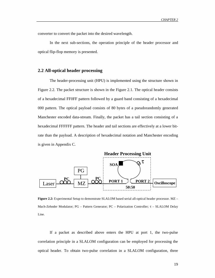
2.2 All-optical header processing
The header-processing unit (HPU) is implemented using the structure shown in
Figure 2.2. The packet structure is shown in the Figure 2.1. The optical header consists
of a hexadecimal FF0FF pattern followed by a guard band consisting of a hexadecimal
000 pattern. The optical payload consists of 80 bytes of a pseudorandomly generated
Manchester encoded data-stream. Finally, the packet has a tail section consisting of a
hexadecimal FFFFFF pattern. The header and tail sections are effectively at a lower bit-
rate than the payload. A description of hexadecimal notation and Manchester encoding
is given in Appendix C.
Figure 2.2: Experimental Setup to demonstrate SLALOM based serial all-optical header processor. MZ –
Mach-Zehnder Modulator; PG – Pattern Generator; PC – Polarization Controller; τ – SLALOM Delay
Line.
If a packet as described above enters the HPU at port 1, the two-pulse
correlation principle in a SLALOM configuration can be employed for processing the
optical header. To obtain two-pulse correlation in a SLALOM configuration, three
Header Processing Unit
PORT 1 PORT 2
PC
50:50
SOAτ
PG
MZ Laser OscilloscopePC
ALL-OPTICAL PACKET SWITCH
20
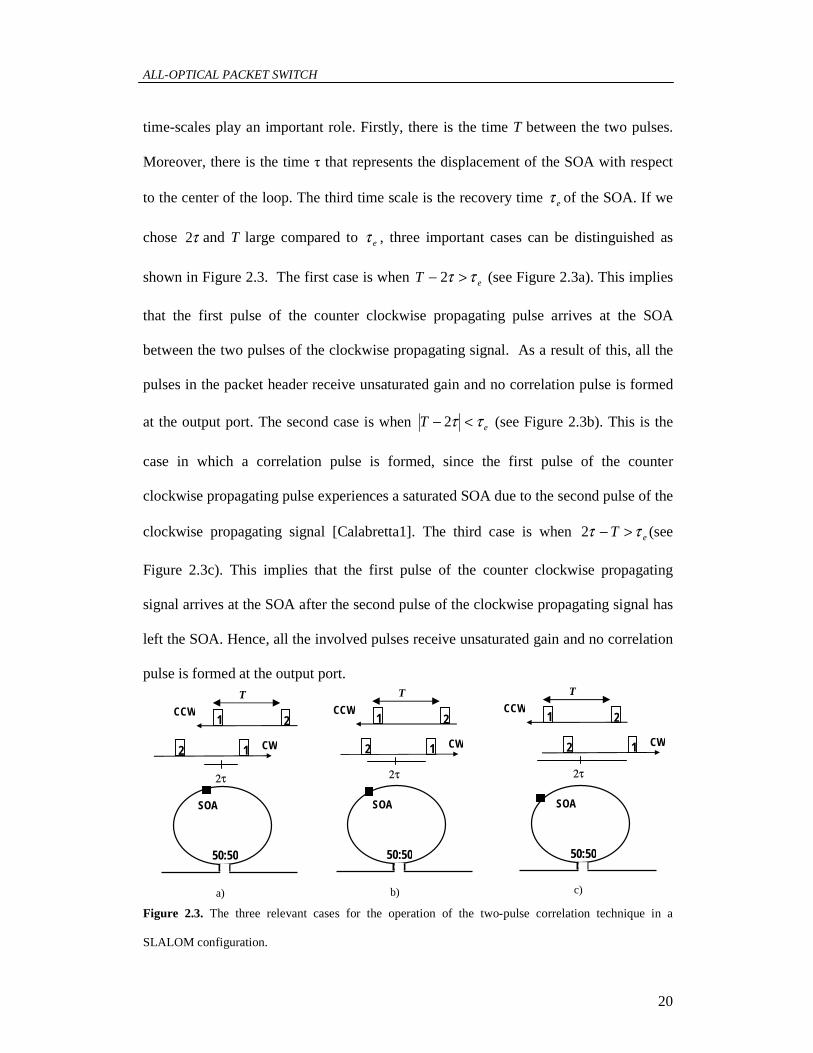
time-scales play an important role. Firstly, there is the time T between the two pulses.
Moreover, there is the time τ that represents the displacement of the SOA with respect
to the center of the loop. The third time scale is the recovery time eτ of the SOA. If we
chose τ2 and T large compared to eτ , three important cases can be distinguished as
shown in Figure 2.3. The first case is when eT ττ >− 2 (see Figure 2.3a). This implies
that the first pulse of the counter clockwise propagating pulse arrives at the SOA
between the two pulses of the clockwise propagating signal. As a result of this, all the
pulses in the packet header receive unsaturated gain and no correlation pulse is formed
at the output port. The second case is when eT ττ <− 2 (see Figure 2.3b). This is the
case in which a correlation pulse is formed, since the first pulse of the counter
clockwise propagating pulse experiences a saturated SOA due to the second pulse of the
clockwise propagating signal [Calabretta1]. The third case is when eT ττ >−2 (see
Figure 2.3c). This implies that the first pulse of the counter clockwise propagating
signal arrives at the SOA after the second pulse of the clockwise propagating signal has
left the SOA. Hence, all the involved pulses receive unsaturated gain and no correlation
pulse is formed at the output port.
Figure 2.3. The three relevant cases for the operation of the two-pulse correlation technique in a
SLALOM configuration.
2 1 CW
CCW 1 2
T
SOA
50:50
b)
2τ
SOA
50:50
a)
CW 2 1
CCW 1 2
T
2τ
SOA
50:50
c)
CCW 1 2
T
2 1 CW
2τ

CHAPTER 2
21
Suppose that a packet with a hexadecimal FF0FF header enters the HPU. Here we
assume that the time T corresponds to the time represented by the hexadecimal symbol
0 between the header pulses. The header pulses are both represented by the hexadecimal
symbol FF. The delay time τ is chosen so that T - 2τ < τe and thus a correlation pulse is
formed at the output of the header processor. However if a packet with a F000F enters
the HPU, no correlation pulse is formed since the time between the two pulses is so
large that the first pulse of the counter clockwise propagating signal arrives at the SOA
after the second pulse of the clockwise signal. Hence both pulses receive unsaturated
gain and no correlation pulse is formed. The high bit-rate optical payload is suppressed
because it drives the SOA in saturation. In order to obtain efficient suppression of the
payload, a tail section is necessary to guarantee that the SOA remains in saturation
when the payload passes through. A tail section could be useful in applications where
the packet size is variable, and packet length information is needed.
Manchester encoding of the packet payload is used to achieve a crucial criterion
of the header processor, the need to differentiate between header and payload. By
Manchester encoding the payload, it is ensured that the header sequence will never be
duplicated in the payload. Therefore the payload will never be able to produce the
correlation pulses made by header data streams. In addition the Manchester encoding
increases the suppression of the payload by keeping the SOA in saturation when the
payload passes through. The saturated SOA can only provide a limited gain to the
payload. The tail section is included to ensure that the SOA stays saturated for the entire
payload. The disadvantage of Manchester encoding is the loss of effective bit rate in the
payload; however, this is offset by benefits such as easier clock recovery in packet
switched applications.

ALL-OPTICAL PACKET SWITCH
22
2.3 All-optical flip-flop memory
The all-optical flip-flop memory employed in the packet switch of Figure 2.1 is based
on two coupled lasers with separate laser cavities [Hill3]. The device is schematically
depicted in Figure 2.4. The system can have two states. In State 1 light from Laser 1
suppresses lasing in Laser 2. In this state the optical flip-flop memory emits continuous
wave light at wavelength λ1. Conversely, in State 2, light from Laser 2, suppresses
lasing in Laser 1. In state 2, the optical flip-flop memory emits continuous wave light at
wavelength λ2.
To change states, lasing in the dominant laser can be stopped by injecting external
light different from the dominant laser’s lasing wavelength. The output pulse of the
optical header processor is used, to set the optical flip-flop memory into the desired
wavelength.
Figure 2.4: Arrangement of two coupled identical lasing cavities, showing the possible states. In State 1,
light from Laser 1 suppresses lasing in Laser 2. In State 2, light from Laser 2 suppresses lasing in Laser
1. To change states lasing in the master is stopped by injecting light not at the lasing wavelength.
Details about the all-optical flip-flop memory can be found in [Hill3]. In brief, it is
shown that the optical flip-flop memory can be described by four coupled differential
State 1
State 2
Master - lasing Slave-not lasing external light not at λ1
to turn off laser 1
Master - lasing
λ 2 output
Slave - not lasingexternal light not at λ2
to turn off laser 2
λ 1output
Laser 1 − λ1
Laser 1 − λ1
Laser 2 − λ2
Laser 2 − λ2

CHAPTER 2
23
(rate) equations, representing the carrier densities and photon densities of each laser
respectively. From the rate equations two important results with respect to the operation
of the all-optical packet switch are presented in [Hill3].
The first result concerns the switching power of a symmetric system of two coupled
lasers. It was demonstrated in [Hill3] that changing the laser current I and the facet
reflectivity R changes the laser output power and also the flip-flop switching power.
However, the optical switching power can be varied independently from the laser
output power by changing the coupling parameter between the lasers, η, [Hill3]. In
Figure 2.5, the output power of the two coupled lasers versus increasing external light
(switching power) is shown. On the horizontal axis the increasing optical power of
external light that is injected into Laser 1 is plotted. The vertical axis represents the
output power of Laser 1 and Laser 2. It is clearly visible that if the amount of external
light that is injected into Laser 1 exceeds a critical threshold level (here about 0 dBm),
Laser 1 switches “off” and Laser 2 switches “on”.
Figure 2.5: Output power of the two coupled lasers versus increasing external light injected into Laser 1.
The solid curve represents the output power of laser 1 (1549.32 nm). The dotted curve represents the
output of laser 2 (1552.52 nm). It is clearly visible that laser 1 switches “off” and laser 2 switches “on”.
The external injected light is at the wavelength λs (1560.61 nm ).

ALL-OPTICAL PACKET SWITCH
24
The property that the optical flip-flop memory can change states with low switching
power is important for the design of the optical packet switch. It makes it possible to
bias the optical flip-flop in such a way that it can be set or reset by the optical header
processor output. The flip-flop can distinguish between the difference in optical power
of the correlation pulse and the suppressed payload, by biasing the laser currents in such
a way, that the optical switching power is exceeded by the correlation pulse but not by
the suppressed payload.
The second result discussed in [Hill3] is the stability for coupled laser systems. The
underlying concept for the operation of the optical flip-flop memory is suppression of
the lasing modes by injection of external light. In principle, there are two different cases
of stability. In the first case, the coupling parameter between the two lasing cavities is
weak. With this it means that the maximum amount of light that is coupled from Laser
1 into Laser 2 and from Laser 2 into Laser 1 is insufficient to suppress lasing. Hence,
for a sufficient injection current I both the lasers are above threshold and lasing with the
identical power.
In the second case, the coupling parameter between the two lasing cavities is so
strong that the amount of light that is coupled from Laser 2 into Laser 1 or from Laser 1
into Laser 2 is sufficient to suppress lasing. In this case lasing in one of the lasers is
suppressed and only one of the coupled lasers is lasing. The system is now either in
State 1 if Laser 1 is lasing or in State 2 when Laser 2 is lasing.
If the system of two coupled laser diodes is biased asymmetrically the system
can form an all-optical threshold function [Hill3]. The system of two coupled lasers can
be made asymmetric by setting the bias current I differently for Laser 1 as for Laser 2.
The system of two coupled lasers is now an optical threshold function (OTF) instead of
an optical flip-flop memory.

CHAPTER 2
25
2.4 All-optical packet switch: experiments
The experimental setup to demonstrate an all-optical packet switch is presented
schematically in Figure 2.6. The set-up that is presented in Figure 2.6 employs all the
functionality that is described in Figure 2.1. It contains an optical header processor
based on the two-pulse correlation principle in a SLALOM configuration, an optical
flip-flop memory based on two coupled lasers and a wavelength routing switch based
on cross-gain modulation.
In the particular experiment, the data rate of the packet payload was 2.5 Gbit/s.
The header pattern was repeated for a duration of 7.5 µs. The payload consists of a data
stream of 35 µs of Manchester encoded pseudo-randomly generated bits. Header and
payload were separated by 5 µs of guard time. The time between to packets was 17.5
µs. Packets with two kinds of headers were employed in the experiments. The first
packet header (Header 1) consists of a repeated hexadecimal FF0FF00 pattern. The
second packet header (Header 2) consists of a repeated hexadecimal 0000000 pattern.
Packets with alternating headers were used throughout the experiments. The optical
power of an optical packet arriving at the packet switch is split in two equal parts. Half
of the optical power of the packet is delayed by 2.8 km fiber and injected into a
wavelength converter. The other half of the optical power is fed into the header
processor.
Suppose a packet with Header 1 enters the SLALOM that is employed for header
processing. In Section 2.2.2, it is discussed that the two-pulse correlation principle of
SLALOM causes a correlation pulse to appear at the SLALOM’s output. The high bit-
rate payload is suppressed because the SOA is driven into saturation [Srivatsa,
Calabretta1].

ALL-OPTICAL PACKET SWITCH
26
Figure 2.6: Experimental set-up to demonstrate the 1×2 all-optical packet switch. Traffic from the
network is coupled in the packet switch at the input. The packet format is given. SOA is Semiconductor
Optical Amplifier, FBG is Fiber Bragg Grating, EDFA is Erbium Doped Fiber Amplifier, ISO is Isolator
and PHASAR is Phased array demultiplexer.
The SOA current in the SLALOM was 136 mA and the averaged input power of the
data packets was –3 dBm. The SLALOM’s output is then passed through an OTF to
differentiate more strongly between the correlation pulse and the suppressed payload.
The SOAs in the OTF were pumped with 135.6 mA and 198 mA respectively. The
threshold function increases the contrast between the correlation pulse and the
suppressed payload from 3 dB at the output of the SLALOM to over 25 dB. The
operation of the OTF is explained in detail in [Hill3]. The output of the threshold
function is then amplified by an EDFA and filtered. If a packet with Header 2 enters

CHAPTER 2
27
the SLALOM structure, then no correlation pulse is formed and consequently, no pulse
is generated by the optical header processor [Srivatsa, Calabretta1].
The output of the header processor produces an optical pulse when there is a
packet containing Header 1, indicating that the packet should be routed to wavelength
λ1. The optical power of the pulse is split into two parts. One half of the pulse is sent
directly to the set input of the optical flip-flop. This pulse sets the output wavelength of
the flip-flop to wavelength λ1. The other half is delayed by 12.5 km fiber and resets the
flip-flop output back to wavelength λ2, after a delay equal to the packet length. The
SOAs in the flip-flop were pumped with 250 mA and 220.9 mA of current respectively.
The optical flip-flop memory implemented here employed coupled ring lasers using
Fabry-Perot filters with a bandwidth of 0.18 nm as wavelength selective elements,
corresponding to the wavelength λ2 and λ1 respectively. This implementation provided a
low noise light source suitable for wavelength conversion. It is clearly visible in Figure
2.5 that the difference in output power between the two states is over 45 dB. The
threshold function was implemented using two coupled lasers made from SOAs and
fiber Bragg gratings as wavelength selective elements.
Finally, the flip-flop output was then fed into a SOA where the packets were
converted to the flip-flop output wavelength via cross-gain modulation [Hill1]. The
SOA that was used for wavelength conversion was pumped with 386 mA of current.
The output of the wavelength converter SOA was then passed through a phased array
demultiplexer to spatially separate the two output wavelengths.
All the couplers used in the experiment were 50/50 couplers except those couplers used
in the flip-flop. Their coupling ratios are given in Figure 2.6. The wavelength outputs 1
and 2 were converted to electrical signals via photodiodes and observed on an
oscilloscope. Packets with Header 1 and Header 2 were alternatively sent through the
ALL-OPTICAL PACKET SWITCH
28
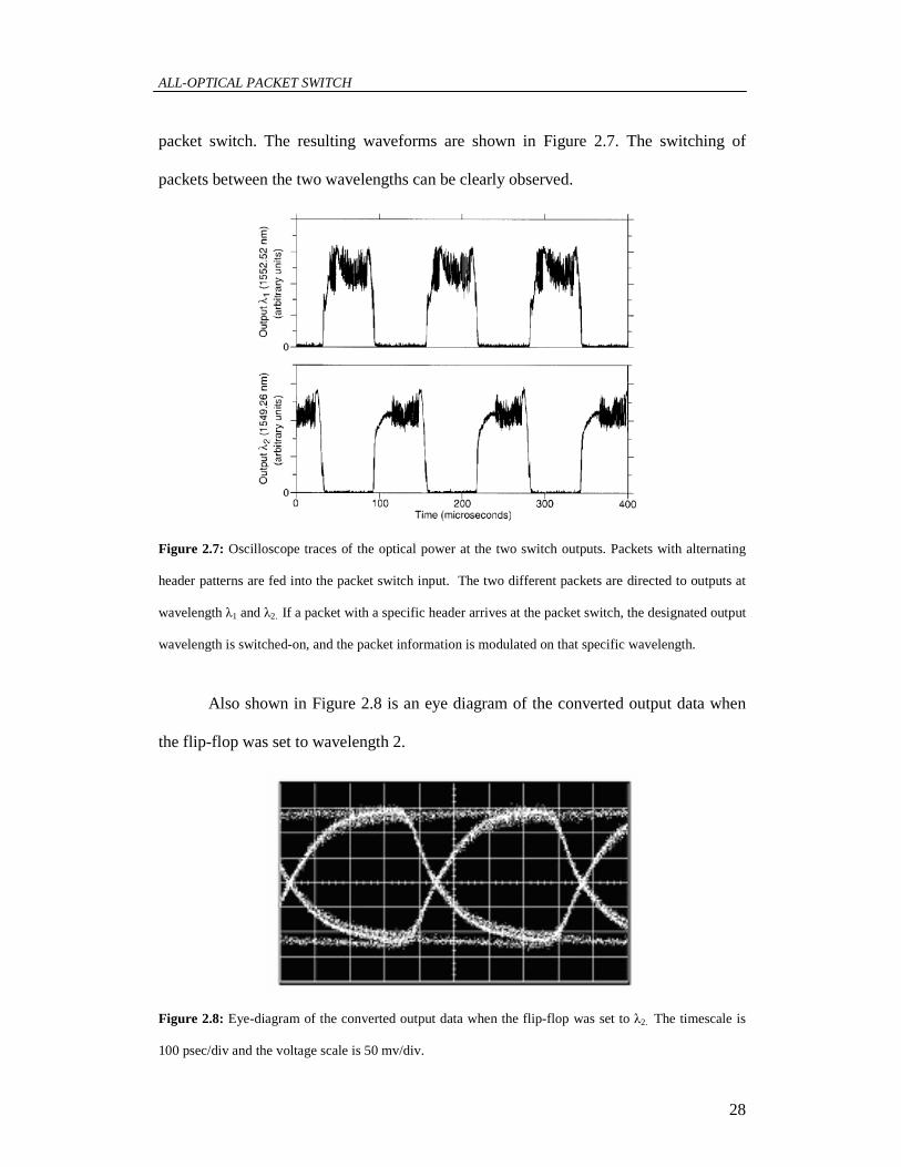
packet switch. The resulting waveforms are shown in Figure 2.7. The switching of
packets between the two wavelengths can be clearly observed.
Figure 2.7: Oscilloscope traces of the optical power at the two switch outputs. Packets with alternating
header patterns are fed into the packet switch input. The two different packets are directed to outputs at
wavelength λ1 and λ2. If a packet with a specific header arrives at the packet switch, the designated output
wavelength is switched-on, and the packet information is modulated on that specific wavelength.
Also shown in Figure 2.8 is an eye diagram of the converted output data when
the flip-flop was set to wavelength 2.
Figure 2.8: Eye-diagram of the converted output data when the flip-flop was set to λ2. The timescale is
100 psec/div and the voltage scale is 50 mv/div.

CHAPTER 2
29
2.5 Conclusions
An advantage of all-optical switching technology over hybrid electro-optical
packet switch technology is that the all-optical approach allows a much higher
processing speed than the hybrid electro-optical approach. In the reported experiment
the packet payload data rate was 2.5 Gbit/s. This was limited by the wavelength
converter, and could potentially reach 100 Gbit/s [Ellis]. The header data rate however
was much slower. This was due to the particular implementation of the optical threshold
function and flip-flop used in the experiment. The lasers used to form these functions
were constructed from standard commercially available fiber pigtailed components
having cavity lengths of many meters. Thus the component lasers had low intrinsic
modulation bandwidths, which limited the speed of the threshold function and the flip-
flop. However integrated versions of these functions using lasers with cavity lengths of
less than a millimeter could attain speeds in the GHz range, allowing high header data
rates and shorter packet lengths. Moreover, by using optical flip-flops that are not based
on coupled laser operation, but on for instance coupled Mach-Zehnder interferometers
ultrafast operation of all-optical flip-flops is possible [Hill2, Hill4]. The laser based
optical flip-flop however provides a high on-off contrast ratio. This makes a laser based
all-optical flip-flop ideal to control a wavelength routing switch with low cross-talk.
The optical header-recognizing concept that is explained in this Chapter is bit-
rate transparent, since the header recognizer based on the SLALOM structure is capable
of recognizing optical packets at different bit-rates. This is true because only the time
between the two pulses plays a role in the header recognition, while the data rate is bit-
rate transparent. The minimum time between the two pulses is limited by the recovery
time of the SOA in the SLALOM. Thus, the set-up as presented in Figure 2.4 can be

ALL-OPTICAL PACKET SWITCH
30
used to recognize an optical header at a data rate of 622 Mbit/s, but two-pulse
correlation can also be successfully demonstrated at 10 Gbit/s header data rates
[Srivatsa, Calabretta1]. Moreover, the contrast between the correlation pulse and the
suppressed payload increases if the payload bit-rate increases. This is due to the gain
saturation of the SOA. If a data-bit passes through, the SOA gain rapidly saturates.
Afterwards the SOA gain slowly recovers. The recovery time of the SOA gain is in the
order of a nanosecond. For a low data-rate (2.5 Gbit/s), the bit-time is about 0.4
nanoseconds. In this time the SOA gain typically recovers by about 50 %. If the data-
rate is higher, the time between two bits is shorter, and thus there is less recovery of the
SOA gain. In the case of high-bit-rate optical data, the clockwise and counter clockwise
signals makes the SOA remain in deep saturation and the entire optical payload is
suppressed. Theoretical analysis predicts about 18 dB suppression for packet payload at
a data rate of 40 Gbit/s. As a result, the threshold function could become redundant.
Thus, since the operation of the optical flip-flop only depends on the presence of a
correlation pulse, the optical header-processing concept is bit-rate transparent for the
header bit-rate, and the routing of the optical payload is based on wavelength
conversion principle that is also bit-rate transparent, it can be concluded that the
proposed all-optical packet switch is bit rate transparent.
Finally, the 1x2 all-optical packet switch concept can be generalized to a 1xN all-
optical packet switch. Crucial is to extend the two-output header recognizer to a multi-
output header processor that can distinguish between a large numbers of header
patterns. In the next Chapter, a multi-output all-optical header processor that can
recognize a large number of header patterns is presented in order to realize a 1xN all-
optical packet switch.


This chapter is based on results published in:
N. Calabretta, Y. Liu, H. de Waardt, M.T. Hill, G.D. Khoe and H.J.S. Dorren, “Multiple output all-optical header processing technique based on two pulse correlation principle,” Electronics Letters, Vol. 37, pp. 1238-1240, 2001.
Chapter 3
Multi-output all-optical header processor
3.1 Introduction In the previous Chapter, an all-optical header processing method based on a two-pulse
correlation principle in a SLALOM configuration has been demonstrated [Srivatsa]. It
was shown that if the packet header is chosen well, a correlation pulse can be generated
at the SLALOMs output (state 1). Alternatively, suppressed payload with much smaller
amplitude arrives at the SLALOMs output (state 2). This header processing method was
successfully employed in a 1x2 all-optical packet switch [Hill1, Dorren1]. The two
states of the packet switch correspond to the two output states of the header processor.
In principle, the concept of the 1x2 all-optical packet switch can be generalized to a
1xN all-optical packet switch. Crucial is then to generalize the header processing
technique presented in Section 2.2.2, which has only one output gate that could have
two different states.

ALL-OPTICAL HEADER PROCESSOR
34
In this Chapter, an all-optical header processing technique that could have N different
output gates is presented. The header processor presents several advantages: the serial
processing nature avoids complicated serial-to-parallel conversion, low power
operation, and this method does not impose a fixed packet length and an external clock.
3.2 Multi-output all-optical header processor
The optical header processor and the data format are presented schematically in Figure
3.1. The optical packet has a header section of 20 bits and a payload section of 74 bytes.
Header and payload are separated by a guard band of 15 bits. The payload is followed
by a tail section of 5 bytes. The optical packet header consists of NRZ data at
effectively lower bit-rate than the payload. The payload is Manchester encoded.
Manchester coding of the payload is necessary to avoid repeated header patterns in the
payload.
Two-pulse correlation technique in a SLALOM configuration has been discussed in
Section 2.2 [Eiselt]. It results that if τ2 and T are chosen large compared to the
recovery time of the SOA, eτ , three important cases can occur[Eiselt, Calabretta1]. In
the first case (condition A) eT ττ >− 2 , no correlation pulse is formed at the output
gate, since all the pulses in the packet header receive unsaturated gain. In the second
case (condition B) eT ττ <− 2 , a correlation pulse is formed, since the first pulse of the
counter clockwise propagating pulse experiences a saturated SOA due to the second
pulse of the clockwise propagating signal. In the third case (condition C) eT ττ >−2 ,

CHAPTER 3
35
no correlation pulse is formed at the output gate, since all the involved pulses receive
unsaturated gain.
Figure 3.1: Experimental set-up to demonstrate SLALOM based serial all-optical header processor. The
optical packets are also shown. HPU1 – Header Processor Unit 1; HPU2 – Header Processor Unit 2; 1τ
– Delay Line for HPU1 ; 2τ – Delay Line for HPU2.
The header processor is implemented as shown in Figure 3.1. The optical power of a
packet arriving at the header processor is split into two equal parts by the optical
splitter. Half of the optical power is fed into the SLALOM structure of HPU1. The other
half of the optical power is fed into the SLALOM structure of HPU2. The SLALOM
structure in HPU1 differs from SLALOM structure in HPU2 by the displacement of the
SOAs with respect to the center of the loop, hence 1τ differs from 2τ .
Packet 1
Packet 2
16ns
59.2ns 14.4ns
0 0 0 0 F 0 0 0 F
F F F F F F F 0 0 0
Tail section (2.5 Gb/s) Manchester Encoded
Payload (10Gb/s)
Header section (2.5Gb/s)
Guard-time 2T
F F F F F F F 0 0 0
Tail section (2.5 Gb/s) Manchester Encoded
Payload (10Gb/s)
Header section (2.5Gb/s)
0 0 0 0 0 F 0 0 F
T 1Guard-time
HPU 1
PC
50:50
SOA1τ1
Output 1
HPU 2
PC
50:50
SOA2 τ2
Output 2
PG
MZ Laser
PC
50:50

ALL-OPTICAL HEADER PROCESSOR
36
Assume packets with two different header patterns. The first packet has a header section
consisting of a hexadecimal ‘F00F0’ pattern corresponding to the time T1 (see Figure
3.1). The second packet has a header section consisting of a hexadecimal ‘F000F’
pattern corresponding to the time T. We choose the displacement times τ1 and τ2 of the
two HPUs in such a way that T1 - 2τ1<τe and T2 -2τ2 <τe.
Suppose that a packet with a header F00F0 enters HPU1. Since T1 - 2τ1<τe (condition B)
a correlation pulse is formed at the output of the header processor. However if the same
packet enters HPU2, no correlation pulse is formed since 2τ2 - T1 > τe (condition C).
Conversely, if a packet with a header F000F arrives at HPU2 a correlation pulse is
formed at output port 2, since the condition B is satisfied. However, no correlation
pulse is formed at output port 1 since T2 -2τ1>τe (condition A).
The high bit-rate optical payload is suppressed because it drives the SOA in saturation.
In order to obtain efficient suppression of the payload, a tail section is necessary to
guarantee that the SOA remains in saturation when the payload passes through
[Srivatsa].
The conditions described above can be used to design the header processor and the
header patterns. It is clear that by matching, the displacement time iτ2 and iT between
the two header pulses, a large number of payload headers can be recognized. Moreover,
the conditions highlight the fact that the speed of the header processor is limited by the
recovery time of the SOA.
In the next Sub-section, experimental results that employ HPUs and the header patterns
designed by using the discussed conditions are presented in order to validate the
concept discussed.

CHAPTER 3
37
3.3 Experiments
The concepts described above are demonstrated experimentally by using the set-up in
Figure 3.1. The WDM source at nm9.1550=λ was modulated by a 10 Gbit/s Mach-
Zehnder modulator, which is driven by an electronic packet generator. The packet
consists of a header and tail section at a 2.5 Gbit/s NRZ data format, and the electrical
payload format consists of a 10 Gbit/s Manchester encoded PRBS data stream. The
average optical power was –1.73 dBm at the input of the optical header processing
system. The SOAs were manufactured by JDS Uniphase and employs a mµ800
strained bulk active region. SOA1 was pumped by 126.9 mA of current, and SOA2 was
pumped by 131.2 mA of current. The displacements of the SOAs in the SLALOM
configuration are set to 12τ =4.8 ns for the HPU1 and 22τ =6.4 ns for HPU2. The
frequency of the signal generator was 9.5132 GHz.
Firstly, data packets with a hexadecimal ‘F00F0’ header pattern enter the header
processor. The photocurrents at output 1 of HPU1 and output 2 of HPU2 are presented in
Figure 3.2. It can be observed from Figure 3.2 that a correlation pulse is formed only at
output 1. The header processor produces a 1.8 ns wide header correlation pulse and 4
ns correlation pulse for the tail. The suppression between the average power of the
payload and the header correlation pulse was 14.39 dB.

ALL-OPTICAL HEADER PROCESSOR
38
Figure 3.2: Packet structure and output of the header processor. The average packet payload is
suppressed by 14.39 dB. The timescale is 10 ns/div and the voltage scale is 50 mV/div.
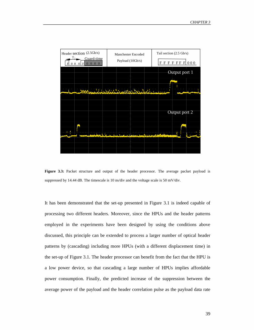
In Figure 3.3, the photocurrents at output 1 and output 2 are presented if a packet with a
hexadecimal “F000F” pattern enters the header processor. It follows from Figure 3.3
that a header correlation pulse is formed only at output 2. The header processor
produces a 1.8 ns wide header correlation pulse and 4 ns correlation pulse for the tail.
The suppression between the average power of the payload and the header correlation
pulse was 14.44 dB.
Output port 2
Output port 1
F F F F F F F 0 0 0
Tail section (2.5 Gb/s) Manchester Encoded
Payload (10Gb/s)
Header section (2.5Gb/s) Guard-time
T1
0 0 0 0 F 0 0 F 0
CHAPTER 3
39
Figure 3.3: Packet structure and output of the header processor. The average packet payload is
suppressed by 14.44 dB. The timescale is 10 ns/div and the voltage scale is 50 mV/div.
It has been demonstrated that the set-up presented in Figure 3.1 is indeed capable of
processing two different headers. Moreover, since the HPUs and the header patterns
employed in the experiments have been designed by using the conditions above
discussed, this principle can be extended to process a larger number of optical header
patterns by (cascading) including more HPUs (with a different displacement time) in
the set-up of Figure 3.1. The header processor can benefit from the fact that the HPU is
a low power device, so that cascading a large number of HPUs implies affordable
power consumption. Finally, the predicted increase of the suppression between the
average power of the payload and the header correlation pulse as the payload data rate
Output port 1
Output port 2
F F F F F F F 0 0 0
Tail section (2.5 Gb/s) Manchester Encoded
Payload (10Gb/s)
Header section (2.5Gb/s)
Guard-time F 0 0 0 F
T 2
0 0 0 0

ALL-OPTICAL HEADER PROCESSOR
40
increases was experimentally confirmed. This could result in a decreasing number of
active components necessary to build the packet switch, since the threshold function
becomes redundant.
3.4 Conclusions
The header processing method employed to demonstrate the 1x2 all-optical
packet switch concept can be extended to recognize a large number of header patterns.
As a result of this the optical packet switch can also be generalized to a 1xN all-optical
packet switch. In order to generalize the all-optical packet switch, a multi-output all-
optical header processor that can distinguish a large number of header patterns has been
demonstrated. The multi-output all-optical header processor is realized by combining
two-pulse correlation technique in a SLALOM configuration and proper designed
header patterns. In particular, each header processing unit is designed to distinguish one
pre-designed header pattern. Conditions to design the header processor units and the
header patterns are also reported. The header processor unit is a low power device. This
makes the header processing unit able to distinguish a large number of header patterns
with an affordable power consumption.
The concept of the multi-output header processor and the design condition have
been demonstrated experimentally. Two header patterns are distinguished at two
distinct output ports by two distinct HPUs. The data rate of the Manchester encoded
payload that was employed in the experiment was 10 Gbit/s (5 Gbit/s effectively). The
measured contrast ratio at one output port between the header correlation pulse and the
suppressed payload was higher than 14.4 dB. This result is in agreement with the

CHAPTER 3
41
predicted increase of the payload suppression as the payload data rate increases. As a
consequence, the threshold function could become redundant. Moreover, the contrast
ratio between the header correlation pulse at one output port with respect to the
suppressed payload at the other output port was also higher than 14.4 dB. In the contest
of a 1xN packet switch, these parameters indicate that only one flip-flop memory can be
set by the optical power of the header correlation pulse, while the optical power of the
suppressed payload is not sufficient to change the original state of the other flip-flops.
This makes the multi-output all-optical header processor suitable for 1xN all-optical
packet switch.


This chapter is based on results published in:
N. Calabretta, Y. Liu, H. de Waardt, M. T. Hill, G. D. Khoe, and H. J. S. Dorren, “Bragg grating assisted all-optical header pre-
processor,” Electronics Letters, Vol. 38, pp. 1560-1561, 2002.
N. Calabretta, Y. Liu, H. de Waardt, M. T. Hill, G. D. Khoe, and H. J. S. Dorren, “All-optical heder processor for all-optical packet
networks’, IEE Proceeding-Optoelectronics, vol. 150, pp. 219-223, 2003.
Chapter 4 All-optical header processor assisted
by an all-optical header pre-processor
4.1 Introduction
To generalize a 1x2 all-optical packet switch into a 1xN all-optical packet
switch, a multi-output all-optical header processor based on two-pulse correlation
principle in a SLALOM configuration was successfully demonstrated in the previous
Chapter. The packet format employed in the experiments to demonstrate the header
processor [Srivatsa, Calabretta1] is shown in Figure 4.1a. The header of the data
packets that were used in the experiments was at a lower bit-rate (2.5 Gbit/s) than the
packet payload (10 Gbit/s). Moreover, the payload was Manchester encoded to avoid
that the header pattern is repeated in the packet payload. The packets had a guard-time
between the header and the payload and a tail section. The length of the guard-time was
equal to the length of the header section. The guard-time section and the tail section
were necessary to adequately suppress the packet payload.

ALL-OPTICAL HEADER PRE-PROCESSOR
44
Figure 4.1: Packet structure of the packets employed in the demonstration of the header processor: a)
packet format employed in the demonstration of the all-optical header processor in the Chapter 3; b) the
simplified packet format employed in the demonstration of the all-optical header processor assisted by an
all-optical header pre-processor is illustrated.
In order to minimize the packet overhead, a Bragg grating assisted all-optical header
pre-processor [Calabretta2, Calabretta3] is presented in this chapter. In the optical
packet switch that is presented in Chapter 2, an optical threshold function is used to
compensate for an insufficient contrast between the correlated header pulses and the
suppressed packet payload. A pre-processing step that discriminates the header and
payload is useful for two reasons. Firstly, it improves the performance of the header
processor so that the optical threshold function becomes redundant. Secondly, the
packet structure could be simplified. We will show that by using the Bragg-grating
assisted all-optical header pre-processor, the guard-time and the tail section become
redundant so that the packet overhead is reduced.
This chapter is organized as follows. In Section 4.2, the concepts of the header pre-
processor are discussed. Experimental evidences are presented as well in order to
confirm the operation of the header pre-processor. In Section 4.3, experimental results
TH TG TP TT
Header (2.5 Gbit/s)
10 Gbit/s Manchester encoded
Payload Tail
T
Guard-time
Header (2.5 Gbit/s)
10 Gbit/s Manchester encoded
Payload
T
a)
b)
CHAPTER 4
45
are presented to show that the header pre-processor improves the performance of the
SLALOM based header processor (enlarge the contrast between the correlation pulse
and the suppressed packet payload) and that the packet structure can be simplified.
Finally, the chapter is concluded with a discussion.
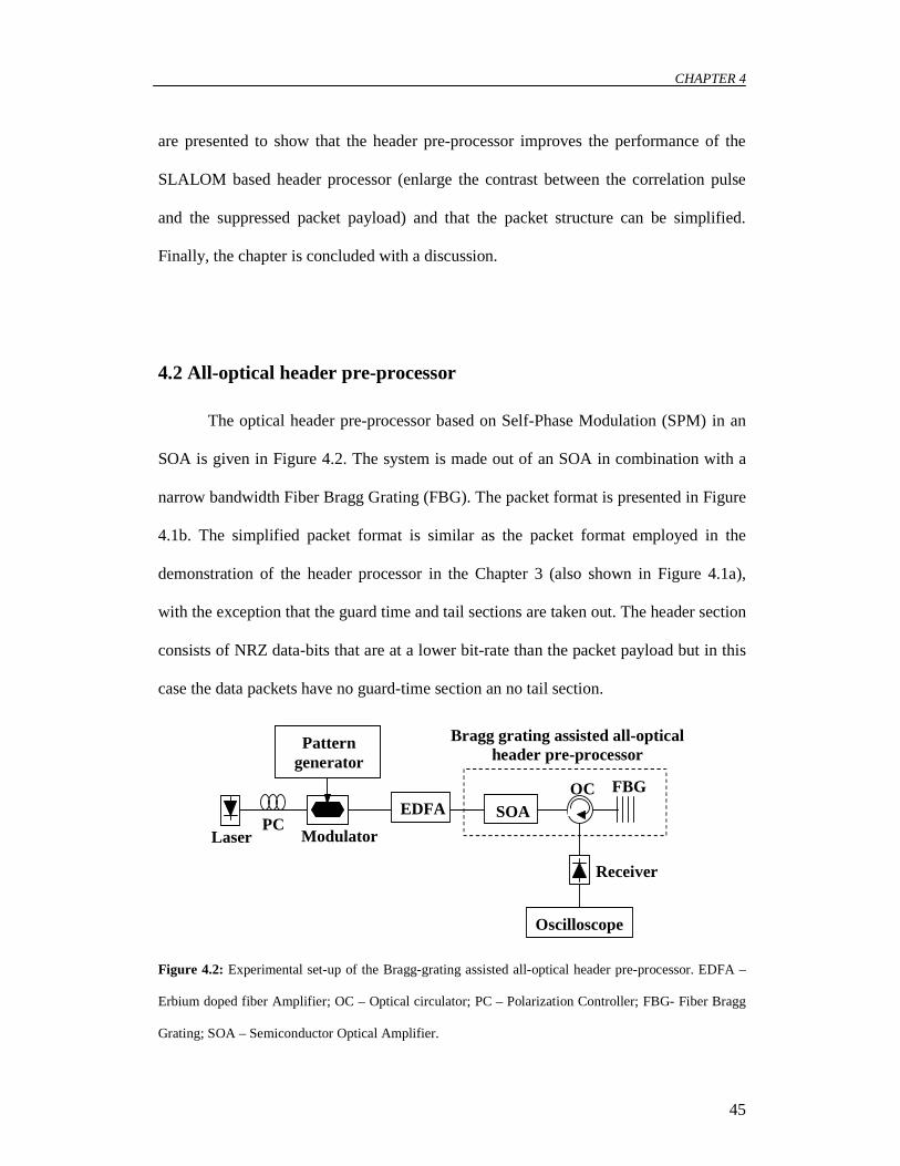
4.2 All-optical header pre-processor
The optical header pre-processor based on Self-Phase Modulation (SPM) in an
SOA is given in Figure 4.2. The system is made out of an SOA in combination with a
narrow bandwidth Fiber Bragg Grating (FBG). The packet format is presented in Figure
4.1b. The simplified packet format is similar as the packet format employed in the
demonstration of the header processor in the Chapter 3 (also shown in Figure 4.1a),
with the exception that the guard time and tail sections are taken out. The header section
consists of NRZ data-bits that are at a lower bit-rate than the packet payload but in this
case the data packets have no guard-time section an no tail section.
Figure 4.2: Experimental set-up of the Bragg-grating assisted all-optical header pre-processor. EDFA –
Erbium doped fiber Amplifier; OC – Optical circulator; PC – Polarization Controller; FBG- Fiber Bragg
Grating; SOA – Semiconductor Optical Amplifier.
EDFA
Laser Modulator
Receiver
Pattern generator
PC
Bragg grating assisted all-optical header pre-processor
Oscilloscope
SOA
FBG
OC

ALL-OPTICAL HEADER PRE-PROCESSOR
46
The packet payload is Manchester encoded. In a Manchester encoded data
stream a binary “1” and a binary “0” is represented by the rising or falling transitions
respectively. Therefore, the average signal power of the payload is constant, regardless
of the specific bit pattern. In the header pre-processing concept, using Manchester
encoded payload is essential to guarantee that the SOA remains in saturation when the
packet payload passes by.
When an optical bit at wavelength λ with sufficient optical power arrives at the
SOA, an overshoot in the amplification at the leading edge of the bit is generated due to
the gain saturation of the SOA, while the rest of the bit experiences a constant saturated
gain. The SOA gain variations also cause SPM and consequently a frequency shift of
the bit that is described by [Agrawal1]:
gdz
d
dt
d αφφπ
ω2
1;
2
1 −=−=
In the equation, ω is the chirp, and g is the SOA gain. Furthermore, α is the linewidth
enhancement factor, and φ is the phase of the bit. Furthermore, z and t are distance and
time respectively. A characterization of these parameters as a function of the SOA drive
current and of the optical input power is reported in Appendix B. The equation
describes the frequency shift as a function of the SOA gain. As a result, the wavelength
at the leading edge of the bit is red chirped ( λλλ ∆+→ ), while the rest of the bit
experiences no chirp. By using a FBG centred around λλ ∆+ , the red chirped leading
edge of the pulse can be filtered out. The amplitude of the filtered leading edge of the
bit depends on the gain of the amplifier.
When an optical data packet is fed into the Bragg grating assisted optical header
pre-processor, a red shift is generated at the leading edge of all the data bits. The time

CHAPTER 4
47
between the pulses in the header has been chosen larger than the recovery time of the
SOA. This results in a strong red shift at the leading edges of the header bits. The
constant averaged optical power of the Manchester encoded payload ensures that the
SOA remains in deep saturation when the payload passes by. Hence, the red shift that is
introduced at the leading edge of the payload bits is small compared to the red shift
introduced at the leading edge of the header bits.
In the next sub-section, two experiments will be performed to show the
operation of the header pre-processor. In the first experiment, the SPM effect in a SOA
as a function of the data rate of the input data signal is investigated. In the second
experiment the operation of the header pre-processor is demonstrated.
4.3 Experiments
The experimental set-up used to demonstrate the concept of the Bragg grating
assisted optical header pre-processor is shown in Figure 4.2. The laser source had a
wavelength of 1558.34 nm and was modulated by a 10 Gbit/s Mach-Zehnder
modulator, which was driven by a pulse-pattern generator. The SOA in the header pre-
processor was pumped with 204 mA of current. The FBG employed had a reflectivity of
99.9 % at λ=1558.93 nm with a bandwidth equal to 0.43 nm. The measured red shift at
the leading edge of the data bit was 0.42 nm.
First, a NRZ encoded PRBS 27-1 data at a bit-rate of 10 Gbit/s is employed in the
experiment. The input data signal is shown in Figure 4.3a, where the PRBS generates a
casual sequences of ‘0s’ between the ‘1’ pulses. Longer sequences of ‘0s’ can be
interpreted as low data bit rate, while short sequences of ‘0s’ can be interpreted as high
data bit rate. The average optical power of the optical packets at the input of the header

ALL-OPTICAL HEADER PRE-PROCESSOR
48
pre-processor is 4 dBm. The output of the header pre-processor is shown in Figure 4.3b.
It consists of pulses with different amplitude corresponding to the leading edges of the
input data signal. The effect of the SPM in a SOA as a function of the data bit rate can
be clearly seen. If the sequences of ‘0s’ between two pulses is longer than the recovery
time of the SOA, the SPM effect is very high, and the amplitude of the leading edges is
high. While if the sequences of ‘0s’ between two pulses is shorter than the recovery
time of the SOA, the SPM effect is low and then the amplitude of the leading edges is
low. The measured contrast ratio between the amplitude of the highest and the lowest
leading edge pulse is higher than 11 dB.
Figure 4.3: Measured oscilloscope traces. The timescale is 500 ps/div and voltage scale 100 mV/div. In
Trace a, the NRZ encoded PRBS data optical signal is shown. In Trace b, the output of the optical header
pre-processor is shown.
In the second experiment, the operation of the header pre-processor is
demonstrated. The packet format is shown in Figure 4.1b. The packets have a header
a)
b)

CHAPTER 4
49
section consisting of NRZ data at a bit-rate of 2.5 Gbit/s, and a payload section
consisting of Manchester encoded PRBS data at a bit-rate of 10 Gbit/s. Note that in
contrast to the results presented in [Srivatsa, Calabretta1], the packets used in this
experiment have no guard-time in between the header and the payload and no tail
sections. Sequential optical packets with two different header patterns are used in the
experiments. The first header (Header 1) has a ‘1100 0000 1100’ bit pattern. The ‘11’
symbol represents the header pulse. The sequence of ‘0s’ represents the time in between
the header pulses. The second header (Header 2) has a ‘1100 0000 0011’ bit pattern. In
Figure 4.4a packets with Header 1 and Header 2 are shown. The average optical power
of the optical packets at the input of the header pre-processor is 4 dBm. The
oscilloscope trace of the signal at the output of the Bragg grating assisted header pre-
processor is presented in Figure 4.4b. It is clearly visible in Figure 4.4b that the header
pre-processor generates a pulse at the leading edges of the header bits. The averaged
suppression of the packet payload is 11.4 dB.
These experimental results conclude that a Bragg grating assisted all-optical header pre-
processor can discriminate the header at lower data rate than the payload. The payload
suppression increases as the data rate increases. Operation at a header bit-rate of 2.5
Gbit/s and a payload data rate of 10 Gbit/s has been demonstrated. However, operation
at higher bit-rate may be possible by decreasing the gain recovery time of the SOA
[Girardin]. Moreover, the design of the optical header pre-processor involves only a
single SOA and an optical filter, thus the system could be integrated in a photonic
integrated circuit.
In the next Section experimental results will be presented to demonstrate that the
header pre-processor improves the performance of the optical header processor based
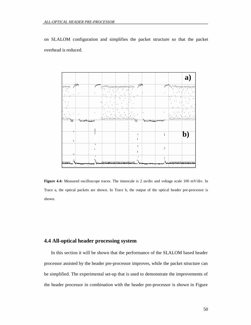
ALL-OPTICAL HEADER PRE-PROCESSOR
50
on SLALOM configuration and simplifies the packet structure so that the packet
overhead is reduced.
Figure 4.4: Measured oscilloscope traces. The timescale is 2 ns/div and voltage scale 100 mV/div. In
Trace a, the optical packets are shown. In Trace b, the output of the optical header pre-processor is
shown.
4.4 All-optical header processing system
In this section it will be shown that the performance of the SLALOM based header
processor assisted by the header pre-processor improves, while the packet structure can
be simplified. The experimental set-up that is used to demonstrate the improvements of
the header processor in combination with the header pre-processor is shown in Figure
a)
b)

CHAPTER 4
51
4.5. It consists of two main parts enclosed in the dash box; the header pre-processor
discussed in the previous section, and the header processor based on SLALOM
configuration.
Figure 4.5: Experimental set-up of the Bragg-grating assisted all-optical header pre-processor in
combination with an optical header processor based on two-pulse correlation in a SLALOM
configuration. EDFA – Erbium doped fiber Amplifier; OC – Optical circulator; PC – Polarization
Controller;τ – Delay of the SOA in the SLALOM; SOA – Semiconductor Optical Amplifier; FBG- Fiber
Bragg Grating.
The concept of an optical header processor unit based on two pulse correlation in a
SLALOM configuration was explained in the Section 2.2 and the design conditions to
realize a multi-output header processor by cascading several header processing units
was discussed in Section 3.2. Such a header processing unit can be implemented as
shown in the dashed box in Figure 4.5. The data format is shown in Figure 4.1b. The
optical packet consists of a header section and a payload section. The optical packet
header consists of NRZ data at effectively lower bit-rate than the packet payload.
Oscilloscope
SOA EDFA
Filter
FBG
SLALOM Laser Modulator
Receiver
OC
SOA
PC
Pattern generator
PC
τ
A
Header Pre-Processor

ALL-OPTICAL HEADER PRE-PROCESSOR
52
Manchester coding of the payload is necessary to avoid repeated header patterns in the
payload [Srivatsa, Calabretta1].
Assume that two packets with two different header patterns are used in the
demonstration. The first header (Header 1) has a header section consisting of a ‘1100
0000 1100’ bit pattern corresponding to the time T1 (see Figure 4.6). The second header
(Header 2) has a header section consisting of a ‘1100 0000 0011’ bit pattern
corresponding to the time T2. Assume that the header pre-processor is the same of that
demonstrated in the previous Section. Moreover, assume that the SLALOM based
header processing unit illustrated in Figure 4.5 has a displacement of the SOA with
respect to the center of the loop equal to τ1 in such a way the relationship T1 - 2τ1<τe (τe
is the electron-hole recombination time) is satisfied.
Following the set-up shown in Figure 4.5, the two sequential packets are first
pre-processed by the header pre-processor. As a result, the output of the header pre-
processor consists of two pulses corresponding to the leading edges of the header pulses
while the data payload is suppressed. The output of the header pre-processor is fed into
the header processing unit. In the Section 3.2 it has been shown that if the displacement
times τ1 of the header processing unit satisfy both the relationships T1 - 2τ1<τe and T2 -
2τ1 <τe, only for packet with Header 1 a correlation pulse is formed at the output of
HPU, while no correlation pulse is formed at the output of HPU when a packet with
Header 2 is processed. Although the operating principle of the header processing unit
does not change, no tail or guard time sections have been employed to suppress the data
payload, since the payload has been previously suppressed by the header pre-processor.
This results in a reduction of the packet overhead (guard-time and tail sections are
redundant). In the following sub-section, experimental results are presented that
CHAPTER 4
53
demonstrate the advantages of the header processor assisted by the header pre-
processor.
4.5 All-optical header processing system: experiments
The experimental set-up used to demonstrate the concept of the header processor
assisted by the optical header pre-processor is shown in Figure 4.5. The laser source had
a wavelength of 1558.34 nm and was modulated by a 10 Gbit/s Mach-Zehnder
modulator, which was driven by a pulse-pattern generator. The packets have a header
section consisting of NRZ data at a bit-rate of 2.5 Gbit/s, and a payload section
consisting of Manchester encoded PRBS data at a bit-rate of 10 Gbit/s. Note that in
contrast to the results presented in [Srivatsa, Calabretta1], the packets used in this
experiment have no guard-time in between the header and the payload and no tail
sections. The SOA in the header pre-processor was pumped with 204 mA of current,
corresponding to a saturation gain of 10 dB with CW light. The FBG employed had a
reflectivity of 99.9 % at λ=1558.93 nm with a bandwidth equal to 0.43 nm. The
measured red shift at the leading edge of the data bit was 0.42 nm.
Sequential optical packets with two different header patterns are used in the
experiments. The first header (Header 1) has a ‘1100 0000 1100’ bit pattern. The ‘11’
symbol represents the header pulse. The sequence of ‘0s’ represents the time in between
the header pulses. The time between the leading edges of the two header pulses is equal
to T1=3.2 ns. The second header (Header 2) has a ‘1100 0000 0011’ bit pattern. In this
case the time between the leading edges of the two header pulses is equal to T2=4 ns. In
ALL-OPTICAL HEADER PRE-PROCESSOR
54
Figure 4.6a packets with Header 1 and Header 2 are shown. The average optical power
of the optical packets at the input of the header pre-processor is 4 dBm.
In order to demonstrate that the use of the Bragg grating assisted header pre-
processor improves the performance of a SLALOM based header processor [Srivatsa,
Calabretta1], the packets are first pre-processed by the header pre-processor. Then, the
output of the header pre-processor is fed into the SLALOM based optical header
processor (see Figure 4.5). The oscilloscope trace of the signal at the output of the
Bragg grating assisted header pre-processor is presented in Figure 4.6b (measured at
point A in Figure 4.5). It is clearly visible in Figure 4.6b that the header pre-processor
generates a pulse at the leading edges of the header bits. Moreover, the time between
the header pulses of the first and second header pattern remains equal to T1 and T2,
respectively.
The output of the header pre-processor is fed into the header processing unit. The SOA
in the SLALOM configuration was pumped with 119 mA of current. The displacement
of the SOA with respect to the centre of the loop is τ =1.6 ns. The displacement of the
SOA matches with the time T1 between the leading edges of pulses in Header 1. Thus, a
correlation pulse is expected to be formed at the output of the header processor only for
optical packets with Header 1.
This is confirmed in Figure 4.6c where it is clearly visible that only for the packet with
Header 1 a correlation pulse is formed. The contrast ratio between the average optical
power of the header correlation pulse and the suppressed payload is equal to 17.8 dB,
resulting in an improvement of 3.3 dB compared to the results presented in the previous
Chapter.

CHAPTER 4
55
Figure 4.6: Measured oscilloscope traces. The timescale is 2 ns/div and voltage scale 100 mV/div. In
Trace a, the optical packets are shown. In Trace b, the output of the optical header pre-processor
(measured at point A in Figure 4.5) is shown. In Trace c, the output of the SLALOM is presented.
4.6 Conclusions
A simple Bragg grating assisted all-optical header pre-processor that can be
used to enlarge the suppression of the packet payload has been demonstrated.
Increasing the packet payload suppression is important since it makes the optical
threshold function in the packet switch that is presented in [Hill1] redundant, and thus
allows us to simplify the optical packet switch architecture. In order to integrate the
packet switch as a photonic integrated device, a simpler switching architecture is
desirable. Also extension of the 1 x 2 packet switch to a packet switch with more output
gates, makes it attractive to use a header pre-processor [Calabretta2, Calabretta3]. In
b)
c)
T2 T1 a)

ALL-OPTICAL HEADER PRE-PROCESSOR
56
this case a single header pre-processor could replace all the optical threshold functions
that are required at the SLALOM outputs. Thus, leading to a reduction of the number of
active components in the optical packet switch.
Operation of the header pre-processor has been demonstrated for data packets with a
payload data rate of 10 Gbit/s, and an optical header at 2.5 Gbit/s. Operation at higher
bit-rates is possible by decreasing the gain recovery time of the SOA [Girardin].
Moreover, the design of the optical header pre-processor involves only a single SOA
and an optical filter, thus the system could be integrated in a photonic integrated circuit.
It should be remarked that in the header pre-processor only a small portion of the bit
experiences a red-shift and in this specific configuration there is a large loss in the FBG.
Nevertheless, the output of the header pre-processor contains sufficient energy to utilize
the two-pulse correlation principle in the SLALOM configuration.
It has been shown that using an optical header pre-processor makes the guard-
time and the tail section of the optical packets redundant so that the packet overhead is
reduced by more than 50%. A reduced packet overhead improves the efficiency of the
packet switch. The contrast ratio of the header pre-processor is equal to 11.4 dB. If the
SLALOM based header processor operates in combination with the header pre-
processor, it has been shown that the contrast ratio between the header correlation pulse
and the suppressed payload is equal to 17.8 dB, which is an increase of 3.3 dB
compared to the result obtained in the previous Chapter [Srivatsa, Calabretta1].
Finally, a header pre-processor that discriminates between the header pulses and
the data payload can allow the use of an ultrafast optical switch [Sokoloff]-[Schreieck]-
[Patel] as header processor to recognize the position of the second pulse with respect to
the first header pulse. As a result, ultrafast implementation of the header processor is

CHAPTER 4
57
feasible. Moreover, as an important advantage of increasing the switching speed, the
optical delay lines involved in the correlation can be shortened and photonic integrated.
In Chapter 6, an ultrafast switch in combination with the header pre-processor will be
investigated in order to design an ultrafast optical header processor.


This chapter is based on results published in: N. Calabretta, Y. Liu, F. M. Huijskens, M. T. Hill, H. de Waardt, G. D. Khoe, and H. J. S. Dorren, “Optical signal processing based on self-induced polarization rotation in a semiconductor optical amplifier,” IEEE Journal of Lightwave Technology, accepted for publication (February 2004).
Chapter 5 Optical signal processing based on
self-induced nonlinear polarization rotation in a semiconductor optical
amplifier 5.1 Introduction
In the previous Chapters an all-optical header processing system assisted by an all-
optical header pre-processor was demonstrated. The optical signal processing functions
implemented to realize the header processor and header pre-processor are based on a
nonlinear device such as an SOA. In particular, the header processor and header pre-
processor have been realized by employing self-induced effects in a nonlinear SOA
such as SPM or XGM/XPM in a loop mirror (such as SLALOM). These effects occur
when an optical signal introduces a change in a nonlinear medium through which the
signal propagates while the medium reacts back on the signal itself. Other examples of
self-induced effects in a SOA employed to realize all-optical signal processing
functions are all-optical threshold functions [Zhao,Hill3], optical self-synchronization
[Cardakli, Xia, Cotter, Deng] and optical clock recovery [Lee]. Most of these optical
signal-processing functions have been realized by employing self-induced optical

NONLINEAR POLARIZATION ROTATION
60
effects in combination with an interferometer. The evident advantages of realizing an
all-optical signal processing functions based on the self-induced effects in a SOA are
the absence of external controls involved in the processing, and then the asynchronous
operation of the device. As a consequence of these advantages, the total system is
simplified (no synchronization issues or additional active components are required).
Recently, considerable attention has been paid to optical signal processing based on
nonlinear polarization switches [Soto, Manning]. Examples include wavelength
conversion [Liu1] and all-optical flip-flop memories [Liu2]. A model for a nonlinear
polarization rotation switch has been presented in [Dorren2]. The examples mentioned
above are based on nonlinear polarization rotation in an SOA in which the polarization
state of a probe pulse is controlled by external (saturating) pump light. In this Chapter,
experimental results are presented in which the nonlinear polarization switch is driven
by self-induced effects [Calabretta4]. First, Self-induced Polarization Rotation (SPR) in
an SOA is investigated in the context of all-optical signal processing. It will be shown
that the polarization dependent gain saturation model presented in [Dorren2] can be
applied to describe SPR in an SOA. In the case of SPR the role of the saturating control
beam is taken over by the data bits themselves. Furthermore, it will also be shown that
SPR in an SOA in combination with a nonlinear polarization switch can be employed
for all-optical signal processing. In order to illustrate the potential of this concept for
telecommunication technology, an all-optical header processor, an all-optical seed pulse
generator, and an optical arbiter based on SPR are presented. Finally, experimental
results indicate that optical signal processing functions based on self-polarization
rotation have a higher extinction ratio and a lower power operation compared to similar
functions based on self-phase modulation.

CHAPTER 5
61
The Chapter is organized as follows: In Section 5.2, SPR in an SOA and a
nonlinear polarization switch based on SPR is demonstrated. In Section 5.3,
applications of all-optical signal processing based on SPR are presented. An all-optical
header processing system, an optical seed pulse generator for packet synchronization
and an all-optical arbiter that could be employed in a packet buffer are demonstrated at
a data rate of 10 Gbit/s. The Chapter is concluded with a discussion.
5.2 Self-polarization rotation
The general configuration of a nonlinear polarization switch is depicted in the
dashed box in Figure 5.1. In [Dorren2] a model for nonlinear polarization rotation
driven by polarization dependent gain saturation in a SOA is presented. Details are
provided in Appendix A. In brief, the polarization switch operates in a similar fashion
to a Mach Zehnder Interferometer switch, but the role of the different arms is taken over
by the TE and TM modes of the incoming light. The modes propagate independently
through the SOA but they have indirect interaction via the carriers. In the model
presented in [Dorren2] the TE and TM modes couple to two different reservoirs of
holes. Thus, if the SOA is saturated by an optical control signal, the gain saturation of
the TE mode differs from the gain saturation of the TM mode [Dorren2]. Hence, also
the refractive index change of the TE mode differs from the refractive index change of
the TM mode. If a small probe signal with well-defined polarization is simultaneously
injected into the SOA with a saturating pump signal, a phase difference between the
modes builds up as the light propagates through the SOA. When the two modes
recombine at the polarization beam splitter (PBS), the phase difference determines
which of the output ports of the PBS the signal is switched to [Dorren2].

NONLINEAR POLARIZATION ROTATION
62
Figure 5.1: Experimental set-up that is used to measure self-polarization rotation in a semiconductor
optical amplifier. PC: Polarization Controller, SOA: Semiconductor Optical Amplifier, BPF: Band Pass
Filter, PBS: Polarization Beam Splitter.
In the experiments a commercially available strained bulk SOA (produced by
JDS-Uniphase) was employed. This device is similar to the one that is used in
[Dorren2] and thus the modeling results presented in that reference can be used to
describe the system applications that follow. In [Dorren2] the presence of tensile strain
in the SOA was modeled by using a population imbalance factor f that has to be
determined from characterization measurements. The model presented in [Dorren2] can
also be used to model nonlinear polarization rotation in unstrained SOAs by setting f=1.
In the latter case the nonlinear polarization rotation is described by the different
confinement factors of the TE and TM modes and thus for f=1, the model in [Dorren2]
is equivalent to that presented in [Stephens].
In the case of SPR, the phase difference between the TE and TM modes is
created by the signal itself. When an optical bit with sufficient optical power arrives at
the SOA, the leading edge of the bit introduces gain saturation in the SOA. Since the
SOA gain saturation is polarization dependent, the TE component of the data bit
Laser Attenuator
Power Meter
BPF SOA PC1 PC2
PBS Output port 1
Output port 2
Polarization switch configuration

CHAPTER 5
63
experiences a different gain saturation than the TM component. Thus, the leading edge
of a data bit can introduce a rotation of the polarization state.
5.3 Self-induced nonlinear polarization switch: experiments
In this sub-section, it will be demonstrated that an optical switch can be driven
by SPR. The experimental set-up that is used to demonstrate the SPR concepts is given
in Figure 5.1. The laser source emits Continuous Wave (CW) light at a wavelength of
1550.91 nm that is injected into the polarization switch via an optical attenuator. The
polarization switch consists of a SOA, two polarization controllers (PC’s) and a PBS.
At the PBS the two modes recombine. PC1 is used to adjust the polarization of the input
signal with respect to the SOA layers (the angle between the TE and TM modes is
approximately 45 degrees [Manning]). PC2 is used to adjust the polarization of the SOA
output with respect to the orientation of the PBS. As an initial experiment, to
characterize the population imbalance factor f, we measure the output power at output
port 2 as a function of the pump current. The attenuator was set in such a way that the
power of the CW-light that enters the SOA via the PC1 was equal to –20 dBm. This
guarantees that the CW-light does not saturate the SOA. PC2 was set in such a way that
no light outputs at port 2. The solid line in Figure 5.2 shows the power at output port 2
as a function of the SOA pump current. It can be observed that the power of output port
2 increases as the pump current increases. The population imbalance factor f can be
determined as a function of the SOA injection current from the curve presented in
Figure 5.2 by following a similar approach as used in [Dorren2]. We find that f varies in
a range of 0.5 and 0.6 if the SOA injection current varies between 70 mA and 390 mA.
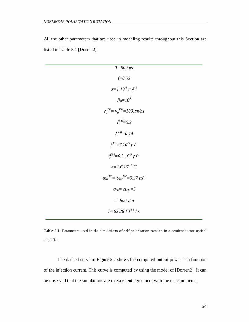
NONLINEAR POLARIZATION ROTATION
64
All the other parameters that are used in modeling results throughout this Section are
listed in Table 5.1 [Dorren2].
T=500 ps
f=0.52
κ=1 10-3 mA-1
N0=108
vgTE= vg
TM=100µm/ps
ΓTE=0.2
ΓTM=0.14
ξTE=7 10-9 ps-1
ξTM=6.5 10-9 ps-1
e=1.6 10-19 C
αintTE= αint
TM=0.27 ps-1
αTE= αTM=5
L=800 µm
h=6.626 10-34 J s
Table 5.1: Parameters used in the simulations of self-polarization rotation in a semiconductor optical
amplifier.
The dashed curve in Figure 5.2 shows the computed output power as a function
of the injection current. This curve is computed by using the model of [Dorren2]. It can
be observed that the simulations are in excellent agreement with the measurements.
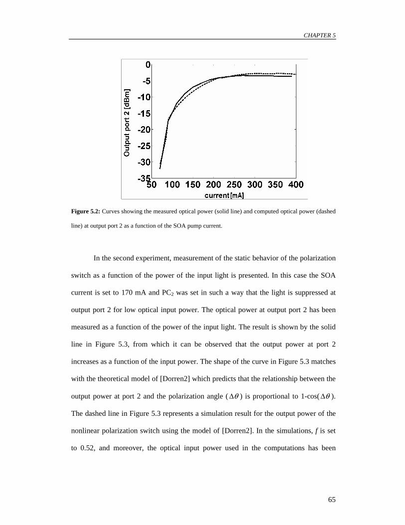
CHAPTER 5
65
Figure 5.2: Curves showing the measured optical power (solid line) and computed optical power (dashed
line) at output port 2 as a function of the SOA pump current.
In the second experiment, measurement of the static behavior of the polarization
switch as a function of the power of the input light is presented. In this case the SOA
current is set to 170 mA and PC2 was set in such a way that the light is suppressed at
output port 2 for low optical input power. The optical power at output port 2 has been
measured as a function of the power of the input light. The result is shown by the solid
line in Figure 5.3, from which it can be observed that the output power at port 2
increases as a function of the input power. The shape of the curve in Figure 5.3 matches
with the theoretical model of [Dorren2] which predicts that the relationship between the
output power at port 2 and the polarization angle ( θ∆ ) is proportional to 1-cos( θ∆ ).
The dashed line in Figure 5.3 represents a simulation result for the output power of the
nonlinear polarization switch using the model of [Dorren2]. In the simulations, f is set
to 0.52, and moreover, the optical input power used in the computations has been

NONLINEAR POLARIZATION ROTATION
66
increased by 4.6 dB to compensate for the insertion losses (1.3 dB for each PC1, and 3.3
dB for the facet losses, including the connector losses).
Figure 5.3: Curves showing the measured optical power (solid line) and computed optical power (dashed
line) at output port 2 as a function of the intensity of the CW input optical power. The inset shows a
zoomed-out view of the switching region.
It is clearly visible in Figure 5.3 that the modeling results are in excellent
agreement with the measured data. In Figure 5.4, the computed gain for the TE and TM
modes is presented. It can be observed that the difference between the TE gain (solid
line) and the TM gain (dashed line) decreases when the input power increases. The gain
difference introduces a phase difference between the modes that results in a rotation of
the polarization angle [Dorren2]. Since the output power at port 2 changes as a function
of the polarization angle ( θ∆ ) according to 1-cos( θ∆ ), for small θ∆ , the transfer
function can be approximated by 2θ∆ . This indicates that a linear change in the input
power leads to a quadratic change in the polarization rotation, and thus a large variation
in the output power.
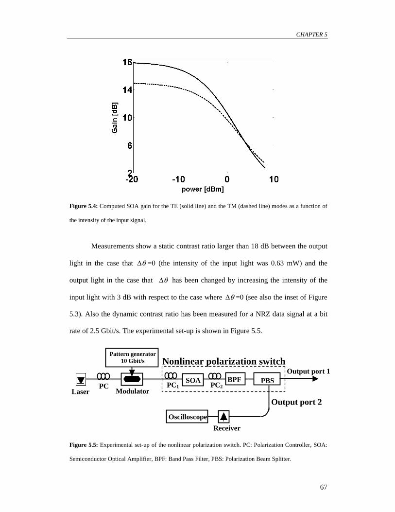
CHAPTER 5
67
Figure 5.4: Computed SOA gain for the TE (solid line) and the TM (dashed line) modes as a function of
the intensity of the input signal.
Measurements show a static contrast ratio larger than 18 dB between the output
light in the case that θ∆ =0 (the intensity of the input light was 0.63 mW) and the
output light in the case that θ∆ has been changed by increasing the intensity of the
input light with 3 dB with respect to the case where θ∆ =0 (see also the inset of Figure
5.3). Also the dynamic contrast ratio has been measured for a NRZ data signal at a bit
rate of 2.5 Gbit/s. The experimental set-up is shown in Figure 5.5.
Figure 5.5: Experimental set-up of the nonlinear polarization switch. PC: Polarization Controller, SOA:
Semiconductor Optical Amplifier, BPF: Band Pass Filter, PBS: Polarization Beam Splitter.
Laser Modulator
PC
Oscilloscope
Receiver
BPF SOA PC1 PC2PBS
Output port 1
Output port 2
Nonlinear polarization switch Pattern generator
10 Gbit/s
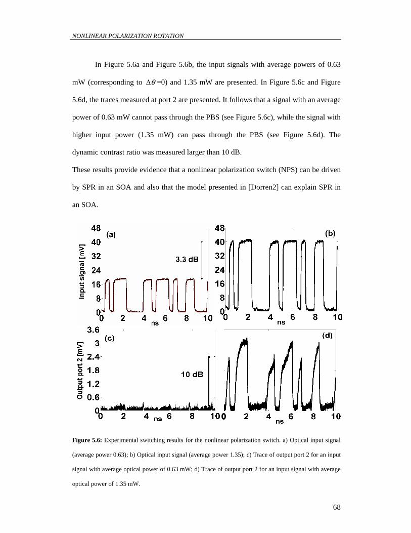
NONLINEAR POLARIZATION ROTATION
68
In Figure 5.6a and Figure 5.6b, the input signals with average powers of 0.63
mW (corresponding to θ∆ =0) and 1.35 mW are presented. In Figure 5.6c and Figure
5.6d, the traces measured at port 2 are presented. It follows that a signal with an average
power of 0.63 mW cannot pass through the PBS (see Figure 5.6c), while the signal with
higher input power (1.35 mW) can pass through the PBS (see Figure 5.6d). The
dynamic contrast ratio was measured larger than 10 dB.
These results provide evidence that a nonlinear polarization switch (NPS) can be driven
by SPR in an SOA and also that the model presented in [Dorren2] can explain SPR in
an SOA.
Figure 5.6: Experimental switching results for the nonlinear polarization switch. a) Optical input signal
(average power 0.63); b) Optical input signal (average power 1.35); c) Trace of output port 2 for an input
signal with average optical power of 0.63 mW; d) Trace of output port 2 for an input signal with average
optical power of 1.35 mW.
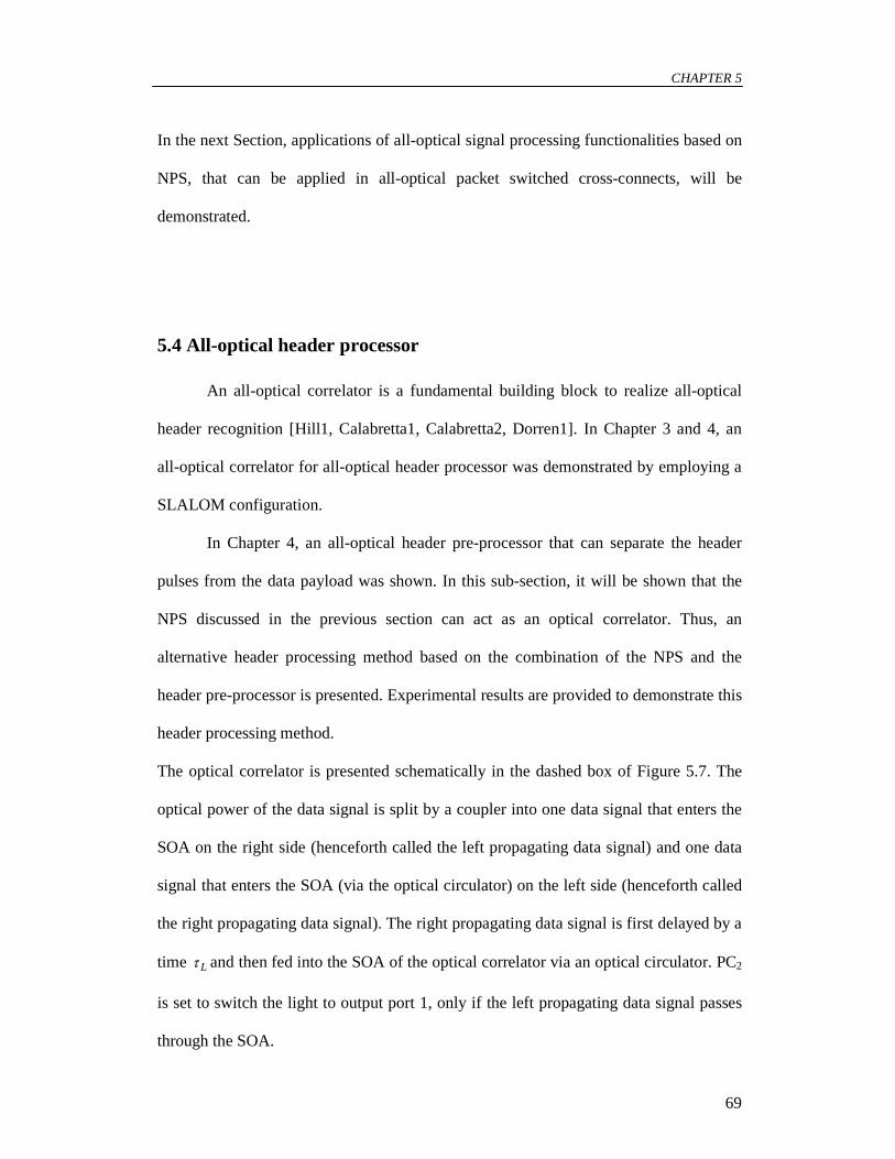
CHAPTER 5
69
In the next Section, applications of all-optical signal processing functionalities based on
NPS, that can be applied in all-optical packet switched cross-connects, will be
demonstrated.
5.4 All-optical header processor
An all-optical correlator is a fundamental building block to realize all-optical
header recognition [Hill1, Calabretta1, Calabretta2, Dorren1]. In Chapter 3 and 4, an
all-optical correlator for all-optical header processor was demonstrated by employing a
SLALOM configuration.
In Chapter 4, an all-optical header pre-processor that can separate the header
pulses from the data payload was shown. In this sub-section, it will be shown that the
NPS discussed in the previous section can act as an optical correlator. Thus, an
alternative header processing method based on the combination of the NPS and the
header pre-processor is presented. Experimental results are provided to demonstrate this
header processing method.
The optical correlator is presented schematically in the dashed box of Figure 5.7. The
optical power of the data signal is split by a coupler into one data signal that enters the
SOA on the right side (henceforth called the left propagating data signal) and one data
signal that enters the SOA (via the optical circulator) on the left side (henceforth called
the right propagating data signal). The right propagating data signal is first delayed by a
time Lτ and then fed into the SOA of the optical correlator via an optical circulator. PC2
is set to switch the light to output port 1, only if the left propagating data signal passes
through the SOA.

NONLINEAR POLARIZATION ROTATION
70
Figure 5.7: Experimental set-up of the header processing system. The packet format of the optical
packets employed in the experiments is also shown. EDFA: Erbium Doped Fiber Amplifier, OC: Optical
circulator, FBG: Fiber Bragg Grating, Lτ : Delay of the counter propagating signal, PBS: Polarization
Beam Splitter; A - Two header pulses (2.5 Gbit/s); B- Alternates ‘1’ and ‘0’ bits (10Gbit/s); C - Sequence
of NRZ ‘0s’ (2.5 Gbit/s).
When the right propagating data signal also enters the SOA, one can distinguish
two cases. In the first case, the optical power of the right propagating data signal is not
sufficient to saturate the SOA. As a result, the left propagating data signal experiences
Header Pre-Processor
Manchester encoded (10 Gbit/s)
A A B B C
Packet format: Payload section Header section
τ
Oscilloscope
Receiver
BPF
Optical correlator
PC1 PC2
OC PBS
τL SOA
Output port 1
Output port 2
SOA EDFA FBG
Laser
OC
Modulator
Pattern generator
PC BPF
BPF
EDFA
CHAPTER 5
71
no polarization rotation. Thus, the left propagating data signal is switched to output port
1. In the second case, the optical power of the right propagating data signal is sufficient
to saturate the SOA. In this case a correlation between the left propagating and the
delayed right propagating data signal is formed since the left propagating data signal
experiences a saturated SOA and thus polarization rotation. As a result, the left
propagating data signal is switched to output port 2. Moreover, the time window in
which pulse correlation can take place is eτ , where eτ is the time that the SOA needs to
recover from the saturation state.
The optical correlator can function as an all-optical header processor as follows.
Output port 2 represents the output of the header processor. Suppose that the header
addresses consist of two header pulses and that the displacement (in time) between two
header pulses is τ (see packet format in Figure 5.7). A header correlation pulse is
formed at output port 2 if eL τττ <− , since the second left propagating header pulse
experiences a saturated SOA introduced by the first right propagating header pulse,
while no header correlation pulse is formed at output port 2 if eL τττ >− or eL τττ >−
since in this case, all pulses propagate through an unsaturated SOA [Calabretta1].
The header processing system is schematically presented in Figure 5.7. It
consists of a header pre-processor (HPP) [Calabretta2] followed by the header
processor discussed above. The optical packet format is also presented in Figure 5.7.
The header section consists of two header pulses that are separated by a sequence of
alternating NRZ ‘0’ and ‘1’ bits at the same bit rate as the data payload, with the
exception of a sequence of ‘0s’ with duration longer than the recovery time of the SOA
which is placed in front of the second header pulse. The position of the second header
pulse within the header section is used to define a unique header pattern. Moreover, the
NONLINEAR POLARIZATION ROTATION
72
space between the second header pulse and the payload is also filled with the sequence
of alternating NRZ ‘0’ and ‘1’ bits. The sequence of alternating NRZ ‘0’ and ‘1’ bits is
used to keep the SOA in saturation when the packet passes through the SOA, while the
sequence of ‘0s’ gives the SOA time to recover before the second header pulse passes
through the SOA. The payload was Manchester encoded to avoid repetition of the
header pattern in the packet payload. Manchester encoding also guarantees that the
average signal power of the payload is constant, regardless the specific bit pattern.
As an example, let’s assume packets with only two different header patterns. The first
packet has a header section consisting of a hexadecimal ‘FAAAAAA00FA’ pattern
(Header 1). For this header pattern, the time between the header pulses is 1τ (see Figure
5.8a). The second packet has a header section consisting of a hexadecimal
‘FAAAAAAA00F’ pattern (Header 2) corresponding to a time 2τ . First, the packets are
pre-processed by an HPP that separates the two header pulses from the packet payload.
The operation of the HPP based on Self-Phase Modulation (SPM) in an SOA is
described in [Calabretta2]. The output signal of the HPP consists of the leading edges of
the two NRZ header pulses while the rest of the packet is suppressed (see Figure 5.8b).
The output of the HPP is fed into the optical correlator based header processor. The
delay Lτ was chosen in such a way that eL τττ <− 1 and eL τττ >−2 . Thus, only a
correlation pulse is formed at output port 2 for packets with Header 1 (since
eL τττ <− 1 ). No correlation pulse is formed at the output port 2 for packets with
Header 2 since eL τττ >−2 .

CHAPTER 5
73
5.4.1 All-optical header processor: experiments
The concepts described above were demonstrated by using the experimental set-
up shown in Figure 5.7. The laser source had a wavelength of 1558.34 nm and was
modulated by a 10 Gbit/s Mach-Zehnder modulator, which was driven by a pulse-
pattern generator. The packet format is shown in Figure 5.7. The packets had a header
section that consisted of two NRZ header pulses at a bit-rate of effectively 2.5 Gbit/s.
The header pulses were separated by a sequence of alternating NRZ ‘0’ and ‘1’ bits at
the same bit rate of the packet payload. The duration of the sequence of ‘0s’ that were
placed in front of the second header pulse was 0.8 ns. The payload section consisted of
Manchester encoded PRBS data at a bit-rate of 10 Gbit/s. The SOA in the HPP was
pumped with 204 mA of current. The FBG employed had a reflectivity of 99.9 % at
λ=1558.93 nm with a bandwidth equal to 0.43 nm.
The optical packets used in the experiment consisted of sequential optical
packets with Header 1 and Header 2 as shown in Figure 5.8a. The time between the
leading edges of the two header pulses was equal to 8.31 =τ ns and 8.42 =τ ns for the
Header 1 and Header 2 respectively. The average optical power of the packets at the
input of the HPP was 4 dBm. The oscilloscope trace of the signal at the output of the
HPP is presented in Figure 4.8b. It is clearly visible in Figure 5.8b that the HPP
generates a pulse at the leading edges of the header bits. The average payload
suppression is 11.4 dB. The output of the HPP is then amplified by an EDFA, filtered
by a 2 nm band pass filter and fed into the header processor (see Figure 5.7). The
average optical power of the left and right propagating signals was –8 dBm and 2.35
dBm respectively (before the optical circulator). The SOA in the header processor was
pumped with 178 mA of current. The PBS has an extinction ratio of 30 dB. The delay

NONLINEAR POLARIZATION ROTATION
74
was Lτ =3.8 ns that matches the time 1τ between the leading edges of pulses in Header
1. Thus, a correlation pulse only for optical packets with Header 1 is expected. This is
confirmed in Figure 5.8c, where a correlation pulse is only formed for packets with
Header 1. The contrast ratio between the average optical power of the header
correlation pulse and the suppressed payload is equal to 18.6 dB. This is an
improvement of 4.4 dB compared to the results presented in [Hill1, Calabretta1,
Dorren1].
The experimental results indicate that the header processing system can
distinguish between two different header patterns. A limitation of this approach is that a
packet header only contains two bits of information. The length of the packet header
can be extended by creating larger packet headers that are built up out of combinations
of two bits (in a similar fashion as in [Calabretta1]). The minimum interval between
different header bits is determined by the SOA recovery time (~ 1 ns).
This means that the duration of the packet is proportional to the number of header bits
times the SOA recovery time. It should be noted however that the SOA recovery time
can be decreased to 60 ps [Girardin]. This means that the length of header patterns can
be reduced with more than a factor 10.
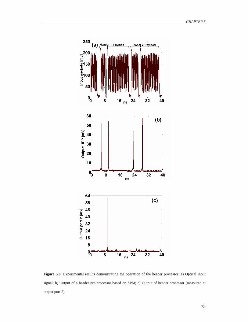
CHAPTER 5
75
Figure 5.8: Experimental results demonstrating the operation of the header processor. a) Optical input
signal; b) Output of a header pre-processor based on SPM; c) Output of header processor (measured at
output port 2).

NONLINEAR POLARIZATION ROTATION
76
5.5 All-optical header pre-processor
In this Section, it will be shown that the NPS of Figure 5.5 can also be used as a
header pre-processor. In this case PC2 is set in such a way that the unsaturated input
data packets are switched to port 2. The header pre-processor can be employed in an all-
optical header processor to discriminate between signals at different data rates as
demonstrated in the previous Sub-section.
When a data pulse enters the NPS, the leading edge will saturate the SOA. In
Section 5.2, it was explained that the SOA gain saturation is polarization dependent,
and hence, rotation of the polarization angle takes place. This ensures that only the
leading edge of a data pulse is switched to output port 2 (at the leading edge the SOA is
not yet saturated), while the rest of the bit leaves the NPS at port 1 (since the SOA is
saturated and the polarization angle of the light is changed).
When a packet with a header as described in the previous subsection enters the
header pre-processor, the leading edges of both header pulses are routed to port 2. The
packet payload and the remainder of the header pulse are switched to port 1.
Assume that the optical packets have a packet format as shown in Figure 5.7.
The sequence of NRZ ‘0s’ placed in front of the NRZ header pulse is longer than the
gain recovery time of the SOA. The transitions of the Manchester encoded data payload
and the alternating ‘1’ and ‘0’ bits in the header section are faster than the gain recovery
time of the SOA. This packet format guarantees that when the optical packet enters the
header pre-processor, only the leading edges of the two NRZ header pulses experience
full gain, while the rest of the packet experiences the SOA in saturation. Thus, the
leading edges of the two header pulses are switched to output port 2 and the rest of the
packet is switched to output port 1.

CHAPTER 5
77
The experimental set-up used to demonstrate the header pre-processor is shown
in Figure 5.5. The laser source had a wavelength of 1550.91 nm and was modulated by
a 10 Gbit/s Mach-Zehnder modulator, which was driven by a pulse-pattern generator.
The packets employed in the experiments are shown in Figure 5.9a. The SOA was
pumped with 141.5 mA of current. The average optical power of the packets measured
before the SOA was –0.2 dBm. The measured output signals at output port 1 and output
port 2 are shown in Figure 5.9b and Figure 5.9c. Output port 2 represents the output of
the header pre-processor. The extinction ratio between the header pulses and the
suppressed payload is larger than 15 dBm, which is an improvement of circa 4 dB with
respect to the HPP presented in [Calabretta2]. In addition, output port 1 provides an
amplified copy of the input packets. Moreover, the header pre-processor operates at
much lower power compared to the HPP presented in [Calabretta2].
In conclusion, an alternative header pre-processor based on an NPS that can
operate at a bit rate of 10 Gbit/s has been demonstrated. Higher operation speed is
possible by decreasing the recovery time of the SOA [Girardin]. This header pre-
processor presents several advantages over HPP: lower power operation, higher
extinction ratio, and an extra output port that provides an amplified copy of the packet.

NONLINEAR POLARIZATION ROTATION
78
Figure 5.9: Experimental results of the header pre-processor based on nonlinear polarization switch. a)
Optical input signal; b) Header pre-processor output (measured at the output port 2); c) Amplified copy
of the input signal (measured at the output port 1).

CHAPTER 5
79
5.6 All-optical seed pulse generator
An optical packet switched cross-connect requires bit-level synchronization and
phase alignment for each packet in order to perform signal processing and routing
[Xia]. Self-synchronization is one of the methods employed to achieve bit-level
synchronization [Xia, Cotter1, Deng]. In general, a self-synchronization method
requires a seed pulse synchronized at the beginning of the packet. The pulse can be used
to generate a local clock for packet synchronization [Cardakli, Xia, Cotter1, Deng,
Sakamoto]. An advantage of the self-synchronization approach is that it is insensitive to
timing jitter between packets or network architectures [Cotter2]. In this Section, an all-
optical seed pulse generator based on the NPS described in the previous section is
presented.
The optical seed pulse generator is schematically shown in Figure 5.10. It consists of an
asymmetric passive Mach-Zehnder Interferometer (MZI) followed by the NPS. The
format of the packets that are used is shown in Figure 5.7.
Figure 5.10: Experimental set-up of the optical seed pulse generator. MZI: asymmetric Mach-Zehnder
Interferometer, dτ : time delay between the two arms of the MZI.
The role of the MZI is to merge the packet with a delayed copy of itself. It is essential
that the delay is shorter than the interval between the header bits. As a result at the MZI
Oscilloscope Receiver
Laser Modulator PC
MZI 50:50 50:50
τd
PC1BPF SOA PC2
Output port 1
Output port 2
Nonlinear polarization switch Pattern generator
PBS
NONLINEAR POLARIZATION ROTATION
80
output the specific packet structure is lost. When the output of the MZI enters the NPS,
only the leading edge of the first NRZ header pulse experiences the unsaturated gain of
the SOA, while the remainder of the data packet experiences a saturated gain. Thus,
only the leading edge of the first NRZ header pulse is switched to output port 2, while
the remainder of the data packet is switched to output port 1. The pulse switched to
output port 2 is synchronized with the beginning of the packet and this represents the
seed pulse.
5.6.1 All-optical self-synchronizer: experiments
The experimental set-up used to demonstrate the optical seed pulse generator is
shown in Figure 5.10. The laser source had a wavelength of 1550.91 nm and was
modulated by a 10 Gbit/s Mach-Zehnder modulator, which was driven by a pulse-
pattern generator. The input packets employed in the experiments are shown in Figure
5.11a. The asymmetry dτ between the two arms of the MZI was measured to be ~ 1 ns.
The SOA was pumped with 142.5 mA of current. The average optical power of the
packets measured before the MZI was 1.5 dBm.
In the first experiment, it will be demonstrated that the optical seed pulse
generator forms a seed pulse synchronized with the beginning of the packet. The output
of the optical seed pulse generator is shown in Figure 5.11b. The seed pulses,
synchronized with the beginning of the packets, are clearly visible. The extinction ratio
between the seed pulse and the suppressed packet is larger than 15 dB.

CHAPTER 5
81
Figure 5.11: Experimental results demonstrating the operation of the optical seed pulse generator. a)
Optical input signal; b) Output of the self-synchronizer (measured at the output port 2).
In the second experiment, it will be shown that the optical seed pulse generator
can still extract timing information, even when the input data packet has an extinction
ratio of 5 dB. This confirms that the optical seed pulse generator can be employed as a
first stage to generate a local clock for synchronization purposes. The optical input
packet is shown in Figure 5.12a. The output of the optical seed pulse generator is
presented in Figure 5.12b.

NONLINEAR POLARIZATION ROTATION
82
Figure 5.12: Experimental results demonstrating the operation of the optical seed pulse generator. The
extinction ratio of the input data packet employed in this experiment is 5 dB. a) Optical input signal; b)
Output of the self-synchronizer (measured at the output port 2).
The seed pulses synchronized with the beginning of the packets are clearly visible in
Figure 5.12b. The measured extinction ratio between the average power of the seed
pulse and the suppressed payload is over 10 dB. However, since PC2 is set in such a
way that the input data are switched to port 2, the power of the guard time between the
packets also leaves port 2. This leads to a reduction of the extinction ratio with 5 dB.
The extinction ratio can be increased by cascading another NPS or an optical threshold
function similar to that presented in [Hill2, Hill3] after the optical seed pulse generator.

CHAPTER 5
83
5.7 All-optical arbiter
The header processing system demonstrated in Section 5.3.1 can only handle
one packet at any given moment. Therefore, optical buffers are necessary to avoid
packet contention. In [Dorren1, Liu3] an all-optical buffering concept is demonstrated
based on a wavelength routing approach. The arbiter function was obtained by using an
optical threshold function. The functionality of the optical threshold function is twofold:
it acts as an arbiter to decide whether packet contention takes place, and it also controls
a wavelength routing switch. The wavelength routing switch consists of a wavelength
converter followed by a demultiplexer. In this Section, a novel all-optical arbiter
function (OAF) based on an NPS that can indicate whether packet contention takes
place is presented.
The OAF consists of a MZI and a NPS as schematically shown in Figure 5.13.
The packet format is shown in Figure 5.7.
Figure 5.13: Experimental set-up for the all-optical arbiter. Tp: time delay equal to one packet slot. dτ :
time delay between the two arms of the MZI
Laser Modulator
Pattern generator
PC
40:60
SOAPC1
MZI 50:50 50:50
τd
Tp
Output port 1 OC BPF
PC2
Output port 2
OscilloscopeReceiver
EDFA BPF
Nonlinear polarization switch
Optical Arbiter
PBS

NONLINEAR POLARIZATION ROTATION
84
It can be distinguished between a packet with low priority (packet 1) and a
packet with high priority (packet 2). Packet 1 enters the NPS via the MZI, while packet
2 enters the NPS via the optical circulator (OC). Let’s assume that the packets arrive
synchronously at the NPS. If no contention takes place, only packet 1 enters the NPS. In
that case the NPS acts as the self-synchronizer discussed before. Thus, a single output
pulse corresponding to the leading edge of the NRZ header pulses is formed at output
port 2.
When packet contention takes place, packet 1 and packet 2 arrive
simultaneously at the NPS. In this case packet 1 experiences a saturated SOA
introduced by packet 2, and thus the polarization angle of packet 1 is rotated. Hence, no
output pulse is formed at output port 2. The OAF can be employed in a buffering
system as follows [Dorren1, Liu3]. The pulse at the output of the OAF (output port 2)
can be used to set/reset a flip-flop memory [Hill1, Hill3, Dorren1]. The output of the
flip-flop controls an optical wavelength routing switch.
5.7.1 All-optical arbiter: experiments
The experimental set-up used to demonstrate the concept of the OAF is shown
in Figure 5.13. The laser source had a wavelength of 1550.91 nm and was modulated by
a 10 Gbit/s Mach-Zehnder modulator, which was driven by a pulse-pattern generator.
The packets employed in the experiment are shown in Figure 5.14a. Two sequential
optical packets were used in the experiments. Packet 1 contains a header pattern
consisting of a hexadecimal ‘FAAAAAA00FA’ bit pattern. Packet 2 contains a header
pattern consisting of a hexadecimal ‘FAAAAAAA00F’ bit pattern. Also visible in

CHAPTER 5
85
Figure 5.14a is a third dummy packet that consists of a sequence of ‘0s’ with a length
equal to the other packets.
Since a single modulated source is employed in the experiment, an optical
coupler has been used to create two sequences of packets to be used as different inputs
of the OAF. One sequence of packets that enters the SOA (via the MZI) on the right
side (left propagating sequence of packets) is shown in Figure 5.14a. The other
sequence of packets that enters the SOA (via the optical circulator) on the left side
(right propagating sequence of packets) is first delayed by Tp as shown in Figure 5.14b.
The time delay Tp was set equal to one packet duration. This ensures that alternating
conditions of packet contention between Packet 1 and Packet 2 take place. The coupler
ratio was chosen to compensate for the different propagation losses experienced by the
left and right propagating sequences of packets. The average optical power of the left
propagating sequence of packets that entered the NPS via the MZI was 1.5 dBm
(measured before the MZI), while the average optical power of the right propagating
sequence of packets that entered the NPS via the OC was 2.2 dBm (measured before the
OC). The SOA was pumped with 126 mA of current.
The output of port 2 of the OAF is shown in Figure 5.14c. It is clearly visible
that when contention takes place, no optical pulse is formed at the output of the OAF.
However, an optical pulse is formed at output port 2 when no contention takes place.
The extinction ratio between the average optical power of the optical pulse and the
suppressed packet is 14.3 dB, enough to drive the optical flip-flop memory [Hill1,
Hill3, Dorren1].

NONLINEAR POLARIZATION ROTATION
86
Figure 5.14: Experimental results demonstrating the operation of the all-optical arbiter. a) Optical input
signal via the asymmetric Mach-Zehnder Interferometer (MZI); b) Optical input signal via the Optical
Circulator (OC); c) Output of the all-optical arbiter (measured at output port 2).

CHAPTER 5
87
5.8 Conclusions
In this Chapter, all-optical signal processing based on self-induced nonlinear
polarization rotation in an SOA has been demonstrated. Experimental and numerical
results confirm that the mechanism behind the self-polarization rotation is the
polarization dependent gain saturation as described in [Dorren2]. It has also been
demonstrated that an NPS based on SPR in a polarization switch interferometer can be
used to achieve optical signal processing functions that are useful for all-optical packet
switching. It should be remarked that an NPS can only be utilized if the polarization of
the input signal is well-defined. In system applications, this could be realized by
employing a polarization independent regenerator in front of the NPS.
An all-optical header processing function at a bit rate of 10 Gbit/s has been
realized, which can distinguish between two different header patterns by employing
nonlinear polarization rotation in an SOA. These results show that by properly
designing the header processor and the header patterns, a large number of different
header patterns can be recognized. The header processor based on SPR has an
extinction ratio between the header correlation pulse and the suppressed payload of 18.6
dB, which is an improvement of 4.4 dB compared with results published in [Hill1,
Calabretta1, Dorren1]. Moreover, it should be noted that the recognition of the header
pattern means the recognition of the position of the second header pulse with respect to
the first header pulse. An advantage of employing a header pre-processor that separates
the header pulses from the data payload, is that an all-optical logic AND can be used as
optical correlator that distinguishes the header pattern. In Section 5.3.1, the all-optical
logic AND has been realized by an NPS. However, the NPS can be replaced by ultrafast
switches such as TOAD, MZI, or UNI. As a result, the header processing method

NONLINEAR POLARIZATION ROTATION
88
discussed in this Chapter can potentially operate at ultrafast speed. Ultrafast processing
will be investigated in Chapter 6.
An all-optical arbiter function at a bit rate of 10 Gbit/s has also been
demonstrated. The arbiter can be used in a buffering system in a similar way as that
presented in [Dorren1, Liu3]. The main difference between our arbiter and the one
presented in [Dorren1, Liu3] is that the output of the arbiter presented in [Dorren1,
Liu3] was a CW signal. In this approach, the output of the arbiter is an optical pulse that
drives the wavelength routing switch via an optical flip-flop [Hill1, Hill3, Dorren1].
A novel optical seed pulse generator at a bit rate of 10 Gbit/s that produces a
seed pulse synchronized with the beginning of the data packet has also been
demonstrated. The seed pulse can be used to generate a local clock for packet
synchronization. Moreover, the operation of the optical seed pulse generator does not
require any particular marker [Cardakli, Xia, Cotter1, Deng] in the packet format that
identifies the beginning of the packet, rather it uses the packet format itself. The
extinction ratio between the seed pulse and the suppressed packet was 15 dB. In
addition, experimental results have shown that a seed pulse can be extracted even with
an input signal extinction ratio of 5 dB, confirming that the optical seed pulse generator
could be used as the first stage in an optical cross-connect node.
Finally, experimental results show that the signal processing functions based on
self-polarization rotation have a lower power operation and a higher extinction ratio
than the same functions based on self-phase modulation.


This chapter is based on results submitted as: N. Calabretta, Y. Liu, H. de Waardt, M.T. Hill, G.D. Khoe and H.J.S. Dorren, “Ultrafast asynchronous multi-output all-optical header processor,” IEEE Photonic Technology Letters, accepted for publication April 2004.
Chapter 6 Ultrafast asynchronous multi-output
all-optical header processor
6.1 Introduction For a practical implementation of an all-optical header processing system utilized in
devising an all-optical packet switch, the header processor should be scalable, high-
speed, have low power consumption and be photonic integrated on a chip. In particular,
scalability defines the capacity of the header processor to recognize a large amount of
header information and eventually to update the system easily to recognize more
headers. High-speed operation is required to match the line-rate of the optical
transmission system so that no bottleneck is generated. Low power consumption and
photonic integration guarantee large scale production, low cost and integration with
other functionalities on the same chip.
Several header processing systems have been proposed that can be used to implement
an all-optical packet switch [Glesk1, Willner]. In [Glesk1], ultrafast all-optical header
processing using a Terahertz Optical Asymmetric Demultiplexer (TOAD) is
demonstrated at a bit rate of 250 Gbit/s. This TOAD based header recognition operates
ASYNCHRONOUS OPTICAL HEADER PROCESSOR
92
at low energy and allows photonic integration, but a disadvantage is that the control
pulse should be synchronized with the header bits. Also, since this header recognition
concept is based on the binary value of a single bit, the header recognizer can only
distinguish between two header patterns. In [Calabretta1], an asynchronous multi-
output all-optical header processing technique based on the two-pulse correlation
principle in a Semiconductor Laser Amplifier in a Loop Optical Mirror configuration
(SLALOM) is presented. This concept was employed in an all-optical packet switch
[Hill1]. This header processing technique does not require a synchronous control pulse,
but the processing speed of the SLALOM based header processor is determined by the
SOA recovery time τr (~ 1 ns) [Eiselt]. Moreover, the SOA has to be placed offset to
the center of the loop with a distance that is larger than τrvg (~ 10 cm) where vg is the
group velocity of light (~ 100 µm/ps). Thus, a disadvantage of the header processing
method presented in [Calabretta1] is that the SLALOM configuration is too large to
allow photonic integration.
In this Chapter, a different header processing technique that can distinguish a large
number of header patterns and which allows asynchronous operation and photonic
integration, is presented. The concept is based on combining the header pre-processor
that is presented in [Calabretta2, Calabretta4] with a TOAD that acts as a header
recognizer. The function of the HPP is twofold: it separates the packet header from the
packet payload, but it also creates the control signal that is required for TOAD
operation. The header pre-processor output is fed into the TOAD for header
recognition. Essential for TOAD operation is the employment of a control pulse for
optical switching [Sokoloff]. Whereas for header recognition based on two-pulse
correlation in a SLALOM configuration, the SOA recovery time plays a critical role,
CHAPTER 6
93
for header recognition based on TOAD operation, the timing of a control pulse is
essential. As a direct consequence of this a header recognizing system based on TOAD
operation allows photonic integration. Moreover, TOAD operation guarantees ultrafast
header processing at low power. Finally, the header processing system as a whole
operates asynchronously and the system can be extended to have multiple output ports.
The Chapter is organized as follows. In Section 6.2, the operation principle of the
header processing technique is presented. In Section 6.3, the experimental results are
shown to validate the header processing operation. Finally, the Chapter is concluded
with a discussion.
6.2 Ultrafast all-optical header processor
The optical header processing system is schematically presented in Figure 6.1. It
consists of a header pre-processor and two TOADs that are placed in parallel. Each of
the TOADs is designed to recognize a specific header pattern.
An essential point of the header processing concept as proposed in this paper, is that the
address information is encoded by the difference in time between the leading edges of
two header pulses. The function of the HPP is to extract the header information form
the data packet. It is shown in [Calabretta4] that this can done by employing self
polarization rotation in a nonlinear polarization switch. The nonlinear polarization
switch is shown in the dashed box of Figure 6.1. In brief, in the nonlinear polarization
switch an optical bit with a polarization angle of approximately 45 degrees in injected
into the SOA. As the bit propagates through the SOA, the polarization angle rotates due
to the polarization dependent gain and index saturation [Calabretta4].

ASYNCHRONOUS OPTICAL HEADER PROCESSOR
94
Figure 6.1 The experimental setup that demonstrates the header processing system and packet structure
are presented. PC: Polarization Controller, EDFA: Erbium Doped Fiber Amplifier, BPF: Band Pass
Filter, PBS: Polarizing Beam Splitter A - Header pulses; B - Alternates ‘1’ and ‘0’ bits; C - Sequence of
‘0’ bits.
Essential however is that the rotation of the polarization angle of the leading edge of the
header bit differs from the rotation of the polarization angle of the trailing edge due to
th_1
Tp
Payload section Header section
th_2
B A A B C
Manchester encoded (10 Gbit/s)
Modulator
PC Laser
BPF SOA PC1 PC2
Header Pre-Processor Pattern generator
10 Gbit/s
Inpu
t Sig
nal
Output port 1
Output port 2
SOA
50:50
Output Control
PC
PBS
Input Port
BPF
90:10
80:20
tc_1 PC
BPF
50:50
Control Signal
EDFA
BPF
∆x
PBS
tc_2
Header 1 processor
PC
SOA
90:10
50:50
PC
PC
50:50
PBS
Input Port
PC
∆x
Manchester encoded (10 Gbit/s)
Header 2 processor

CHAPTER 6
95
self gain saturation. By aligning the polarization of the SOA output carefully with the
polarizing beam splitter, only the leading edge of the header bit outputs the nonlinear
polarization switch [Calabretta4]. The space between the header pulses is filled with a
sequence of alternating NRZ ‘0’ and ‘1’ bits at the same bit rate as the data payload,
which ensures that the SOA remains saturated while the packet header passes through
[Calabretta4]. Also, a series of ‘0’ with a duration that is longer than the SOA recovery
time τr is placed before the second header bit, to allow the amplifier to recover before
the second header pulse arrives at the SOA. Similarly, the guard time in between the
header section and the payload section is filled with a sequence of alternating ‘0’ and
‘1’ bits to keep the amplifier saturated when the packet passes by. Finally, the packet
payload is Manchester encoded to avoid repetition of the header pattern in the packet
payload. Manchester encoding also guarantees that the average signal power of the
payload is constant, regardless the specific bit pattern [Calabretta4].
The operation of the TOAD is described in [Sokoloff]. As shown in the dashed box of
Figure 6.1, a TOAD consists of an optical loop that contains an SOA, which acts as a
nonlinear element. The SOA is placed with an offset ∆x with respect to the center of the
loop. When an optical input pulse enters the TOAD, the pulse power is split by a 50:50
coupler into a clock-wise propagating pulse (CW) and counter-clockwise propagating
pulse (CCW). The optical power of the CW- and CCW propagating pulses should be
lower than the SOA saturation power, thus both pulses experience the same gain and
phase shift when passing through the SOA. Hence, if no control pulse is present, the
recombined CW- and CCW propagating pulses reflect back at the TOAD input port.
The role of the control pulse that is coupled into the loop via a 90:10 coupler is to create
a refractive index change in the SOA. If the control pulse arrives at the SOA after the

ASYNCHRONOUS OPTICAL HEADER PROCESSOR
96
CW propagating pulse has passed through but before the CCW propagating pulse
arrives at the SOA, the CW- and CCW propagating pulses no longer experience the
same gain and refractive index. This leads to the creation of a pulse at the TOAD output
[Sokoloff]. The polarization of the control light is orthogonal with respect to the
polarization of the input pulses. Thus the control light can be removed by using a
Polarizing Beam Splitter (PBS).
The TOAD can function as a header processor as follows. The header pre-processor
output pulses form the TOAD input signal and are split by an 80:20 coupler into a low
power CW- and CCW propagating data signal and a high power control signal. The
CCW propagating pulses arrive at the SOA a time τsw = 2 ∆x /vg later with respect to the
CW propagating pulses. If no control is present the data signal is reflected back to the
TOAD input. The first pulse of the high power control signal is used to saturate the
SOA. Header recognition can be implemented by accurately timing the control pulses.
There are three interesting cases that are shown in Figure 6.2. In the first case (see
Figure 6.2a), the first control pulse arrives at the SOA after the second CCW
propagating data pulse. Thus, the control pulse arrives too late at the SOA to create a
pulse at the TOAD output. In the second case (see Figure 6.2b), the control light arrives
at the SOA after the second CW propagating data pulse has passed through the SOA,
but before the second CCW propagating data pulse arrives at the SOA. Hence, the
control light creates a refractive index change in the SOA that is only experienced by
the second CCW propagating pulse. Hence, a pulse is created at the TOAD output. In
the third case (see Figure 6.2c), the control light arrives at the SOA before the second
CW- and CCW pulses. In this case the SOA refractive index change is experienced by
both the second CW- and CCW pulses. Thus no pulse is formed at the TOAD output.

CHAPTER 6
97
The separation of the two pulses should be large enough to ensure that the control light
cannot switch the first header pulse.
Figure 6.2. Timing of the control pulses for the three relevant cases for the operation of the header
processor; a) The control arrives at the SOA after that all the pulses have passed the SOA; b) The control
arrives at the SOA after that the second CW pulse has passed the SOA but before that the second CCW
arrives at the SOA; c) The control arrives at the SOA before that both the CW and CCW second pulses
arrive at the SOA.
It can be concluded that a pulse is only output from the TOAD if the time between the
two header pulses matches with the timing of the control pulse. The TOAD output pulse
can be used to set/reset an optical flip-flop that controls the optical wavelength routing
switch, similarly as described in Chapter 2. It is important to notice that in contrast to
header recognition based on two-pulse correlation in a SLALOM configuration, this
header recognition concept does not critically depend on the SOA recovery time.
Hence, the offset of the SOA with respect to the center of the loop and the delays for
the control pulses can be made sufficiently small in order for this header processing
concept to allow photonic integration.
Control Control
90:10
CW Signal
CCW Signal
1 2
SOA
50:50 Input Signal
τsw
1 2
2 1
b)
τsw
Control Control
90:10
CCW Signal
CW Signal
1 2
SOA
50:50 Input Signal
2 1
1 2
a)
Control Control
90:10
c)
CCW Signal
1 2
SOA
50:50 Input Signal
τsw
1 2
2 1
CW Signal

ASYNCHRONOUS OPTICAL HEADER PROCESSOR
98
6.3 Experiments
The concepts described above were demonstrated by using the experimental set-up
shown in Figure 6.1. The laser source had a wavelength of 1550.91 nm and was
modulated by a 10 Gbit/s Mach-Zehnder modulator, which was driven by a pattern
generator. The packet format is also shown in Figure 6.1. The duration of the sequence
of ‘0’ bits that were placed in front of the second header pulse was 0.9 ns. The payload
section consisted of Manchester encoded PRBS data at a bit-rate of 10 Gbit/s.
Sequential optical packets with header sections consisting of a hexadecimal ‘D555 5555
5500 3555’ pattern (Header 1) and a hexadecimal ‘D555 5555 5540 1C55’ pattern
(Header 2) were used in the experiments (see Figure 6.3a). This means that the time
between the header pulses are 5 ns and 5.1 ns for Header 1 and Header 2 respectively.
The packets are first pre-processed by the header pre-processor. The average optical
power of the packets at the input of the header pre-processor was 2.3 dBm. The
extinction ratio of the input optical data packet was 12 dB. The SOA in the header pre-
processor was pumped with 123.5 mA of current. The PBS has an extinction ratio of 30
dB. The oscilloscope trace of the signal that outputs the header pre-processor is
presented in Figure 6.3b. It is clearly visible in Figure 6.3b that the header pre-
processor generates a pulse at the leading edges of the header bits. The pulses have a
duration of 50 ps each. The average payload suppression is 18.4 dB. The header pre-
processor output is than split by an 80:20 coupler to create the input- and control signals
of the TOADs. The input and control signal are split by 50:50 couplers before being
distributed over the TOADs. For both TOADs τsw is 50 ps. The control signals were
delayed by 4.95 ns and 5.05 ns before being fed in TOAD 1 and TOAD 2, respectively.

CHAPTER 6
99
Figure 6.3. Measured oscilloscope traces. a) The optical data packets that input the header processor.
Packets with two different headers are shown. The inset shows details of the packet header; b) The output
of the header pre-processor. It is clearly visible that only pulses synchronized with the leading edge of the
header bits output the header pre-processor; c) Output at port 1. It is visible that only packet 1 is
recognized; d) Similarly as in c, but now for packet 2.
b)
c)
d)
Out
put p
ort 2
[mV]
O
utpu
t por
t 1 [m
V]
Out
put H
PP [V
]
Header 1 Header 2 Payload a) In
put p
acke
ts [V
]
Time [ns]
20 21 22 23 24 25 26

ASYNCHRONOUS OPTICAL HEADER PROCESSOR
100
The SOAs in TOAD 1 and TOAD 2 were pumped with 116 mA and 121 mA of current,
respectively. The energy of the input pulses was 50 fJ while the energy of the control
pulses was 0.8 pJ. According to the design of the TOADs and the header patterns, it is
expected that a pulse is formed at output port 1 only for packets with Header 1 and a
pulse is formed at output port 2 only for packets with Header 2. The traces of output
port 1 and output port 2 are shown in Figure 6.3c and 6.3d, respectively. It is clearly
visible that indeed a pulse is formed at output port 1 only for packets with Header 1
while no pulse is formed for packets with Header 2. It can be observed that a pulse is
formed at output port 2 only for packets with Header 2 while no pulse is formed for
packet with Header 1. The contrast ratio between the pulse and the suppressed payload
is higher than 14.4 dB.
These experiments indicate that the set-up presented in Figure 6.1 is indeed capable of
recognizing two different headers but the concept is scalable so that a larger number of
packet headers can be processed. A limitation of this approach is that a packet header
only contains two bits of information. The length of the packet header grows linearly
with the number of packet header times the header processor’s speed (~100 ps). It
should be noted however that the processing speed of the header processor can be
decreased to 4 ps [Sokoloff]. This means that the length of header patterns can be
reduced with more than a factor 25.
6.4 Conclusions
An all-optical header processing system based on combining a single header pre-
processor and two TOADs that act as header recognizers was demonstrated. The header
processing system can distinguish between two different packet headers and the output

CHAPTER 6
101
is sent to two distinct output ports. We believe that this principle can be extended to
recognize more header patterns by constructing packet headers that are made out of a
sequence of two header bits as shown in this paper.
The design of the header processing system provides several key advantages over
alternative techniques. The header pre-processor operates asynchronously so that the
header processing system as a whole can be operated in an asynchronous fashion. The
system also operates as a low power device. In the presented experiments the bit rate
was 10 Gbit/s and τsw was 50 ps, but optical switching of a 250 Gbit/s signal has been
demonstrated using a TOAD for which τsw was 4 ps [Glesk1, Sokoloff]. Thus, we
believe that the header processor can operate at higher bit rates than 10 Gbit/s.
Moreover, a shorter offset time in the order of a few picoseconds allows photonic
integration of the header processor. Finally, a header processing system that can
recognize a large number of header patterns can be utilized in devising an all-optical
packet switch.


Chapter 7 Conclusions
In this section the most important conclusions with respect to the original results that
can be found in Chapter 3 to Chapter 6 of this thesis are given.
In Chapter 3, an all-optical serial header processor is discussed that is capable of
recognizing 2 different packet headers and that forms correlation pulses at two distinct
output ports. This header recognizing principle can be extended to recognize more
header patterns. Our demonstration showed the header processor working with payload
data rates of 10 Gbit/s, however we believe that it is possible to process payloads at
higher bit rates.
The design of the header processor shown in Chapter 2 provides several key advantages
over alternate techniques. Firstly, the serial nature of the header processor removes the
additional complexity of the separation of payload and header sections of the packet
and does not impose a fixed packet length. In addition, the header processor is a low
power device; the amount of input power required can be adjusted by changing the
current into the SOA
In Chapter 4, a Bragg grating assisted all-optical header pre-processor is demonstrated.
The contrast ratio of the header pre-processor is 11.4 dB. It was demonstrated the
operation for data packets with a packet header at a bit-rate of 2.5 Gbit/s and payload at

CONCLUSIONS AND RECOMMENDATIONS
104
a data rate of 10 Gbit/s. Operation at higher bit-rate may be possible by increasing the
gain recovery time of the SOA. Moreover, the design of the optical header pre-
processor involves only a single SOA and an optical filter, thus the system could be
integrated in a photonic integrated circuit.
It was also demonstrated that the header pre-processor improves the performance of the
optical header processor that is used in the packet switch of Chapter 2. The guard-time
and the tail section of the optical packets become redundant so that the packet overhead
is reduced. Moreover, the contrast ratio between the header correlation pulse and the
suppressed payload is equal to 17.8 dB, which is an increase of 3.3 dB compared to the
result obtained in Chapter 2.
Chapter 5 is devoted to all-optical signal processing based on self-induced nonlinear
polarization rotation in an SOA. Experimental and numerical results confirm that the
mechanism behind the self-polarization rotation is the polarization dependent gain
saturation as described in Appendix A. It was also demonstrated that a nonlinear
polarization switch based on self-polarization rotation can be used to achieve optical
signal processing functions that are useful for all-optical packet switching. It should be
remarked that a nonlinear polarization switches can only be utilized if the polarization
of the input signal is well-defined. In system applications, this could be realized by
employing a polarization independent regenerator in front of the nonlinear polarization
switch.
It was realized an all-optical header processing function at a bit rate of 10
Gbit/s, which can distinguish between two different header patterns by employing
nonlinear polarization rotation in a SOA. We believe that by properly designing the
header processor and the header patterns, a large number of different header patterns

CHAPTER 7
105
can be recognized. The header processor based on SPR has an extinction ratio between
the header correlation pulse and the suppressed payload of 18.6 dB, which is an
improvement of 4.4 dB compared with the header processor of the packet switch in
Chapter 2.
It was also demonstrated an all-optical arbiter at a bit rate of 10 Gbit/s. The
arbiter can be used in a buffering system in a similar way as that presented in [Liu1].
The main difference between our arbiter and the one presented in [Liu1] is that the
output of the latter arbiter was a CW signal. In this approach, the output of the arbiter is
an optical pulse that drives the wavelength routing switch via an optical flip-flop
[Hill2].
Also presented in Chapter 5 is a novel optical seed pulse generator that operates
at a bit rate of 10 Gbit/s and produces a seed pulse synchronized with the beginning of
the data packet. The seed pulse can be used to generate a local clock for packet
synchronization. Moreover, the operation of the optical seed pulse generator does not
require any particular marker in the packet format that identifies the beginning of the
packet, rather it uses the packet format itself. The extinction ratio between the seed
pulse and the suppressed packet was 15 dB. In addition, experimental results have
shown that a seed pulse can be extracted even with an input signal extinction ratio of 5
dB, confirming that the optical seed pulse generator could be used as the first stage in
an optical cross-connect node.
Finally, experimental results in Chapter 5 show that the signal processing functions
based on self-polarization rotation have a lower power operation and a higher extinction
ratio than the same functions based on self-phase modulation.

CONCLUSIONS AND RECOMMENDATIONS
106
In Chapter 6, an all-optical header processing system based on combining a single
header pre-processor and two TOADs that act as header recognizers is introduced. The
header processing system can distinguish between two different packet headers and the
output is sent to two distinct output ports. We believe that this principle can be extended
to recognize more header patterns.
The design of the header processing system provides several key advantages over
alternative techniques. The header pre-processor operates asynchronously so that the
header processing system as a whole can be operated in an asynchronous fashion. The
system also operates as a low power device. In this chapter, the bit rate was 10 Gbit/s
and τsw was 50 ps but optical switching of a 250 Gbit/s signal has been demonstrated
using a TOAD for which τsw was 4 ps [Solokoff]. Thus, we believe that the header
processor can operate at higher bit rates than 10 Gbit/s. Moreover, a shorter offset time
in the order of a few picoseconds allows photonic integration of the header processor.
Finally, a header processing system that can recognize a large number of header
patterns can be utilized in devising an all-optical packet switch.


This chapter is based on results published in: H. J. S. Dorren, D. Lenstra, Y. Liu, M. T. Hill, and G. D. Khoe, “Nonlinear polarization rotation in semiconductor optical amplifiers: theory and application to all-optical flip-flop memories,” IEEE Journal of Quantum Electronics, vol. 39, pp. 141-147, 2003.
Appendix A
Model for nonlinear polarization rotation in a semiconductor optical
amplifier In this appendix, a model of nonlinear polarization rotation in a semiconductor optical
amplifier is presented. This model can be found in [Dorren2]. An introduction and the
schematic of the nonlinear polarization switch are presented in Section 5.2. The
incoming arbitrarily polarized electric field was decomposed in a component parallel to
the layers in the waveguide (TE-mode) and a perpendicular component (TM mode).
These two polarization directions are along the principal axes that diagonals the wave
propagation in the SOA. In fact, apart from their indirect interaction through the carrier
dynamics in the device, these two polarizations propagate independently from each
other.
The propagation equation for the TE polarized electric field component ATE(z,t) is
given by:
),(2
1),(),()1(
2
1),( int tzAtzAtzgitzA
zv
tTETETETETETETETE
g αα −+Γ=
∂∂+
∂∂
(A.1)

MODEL FOR NONLINEAR POLARIZATION ROTATION
110
Here, ATE(z,t) is the weakly time and space dependent complex envelope of the optical
field, TEgv the corresponding group velocity taken at the central frequency of the wave,
ΓTE the confinement factor, gTE(z,t) the (real) gain function, αTE the phase-modulation
parameter and TEintα the modal loss. A similar rate-equation holds for the complex field
envelope ATM(z,t) corresponding to the TM mode:
),(2
1),(),()1(
2
1),( int tzAtzAtzgitzA
zv
tTMTMTMTMTMTMTMTM
g αα −+Γ=
∂∂+
∂∂ (A.2)
where ATM(z,t) is the weakly time and space dependent complex envelope of the optical
field, TMgv the corresponding group velocity, ΓTM the confinement factor, gTM(z,t) the
(real) gain function, αTM the phase-modulation parameter and TMintα the modal loss. The
envelopes for each polarization can be expressed as:
),(),( ),(),(),(),( tziTMTMtziTETE TMTE
etzStzAetzStzA φφ == (A.3)
where STE(z,t) and STM(z,t) are the photon numbers and ),( tzTEφ and ),( tzTMφ are the
phases for the TE and TM components.
The two optical modes have indirect interaction via the carriers. It is assumed that
the TE and TM polarizations couple the electrons in the conduction band with two
distinct reservoirs of holes. This assumption is justified by the fact that in zincblende
structures such as GaAs and InP the optical transitions occur between j=1/2 type
conduction band states and the j=3/2 type valence band states, where the latter are
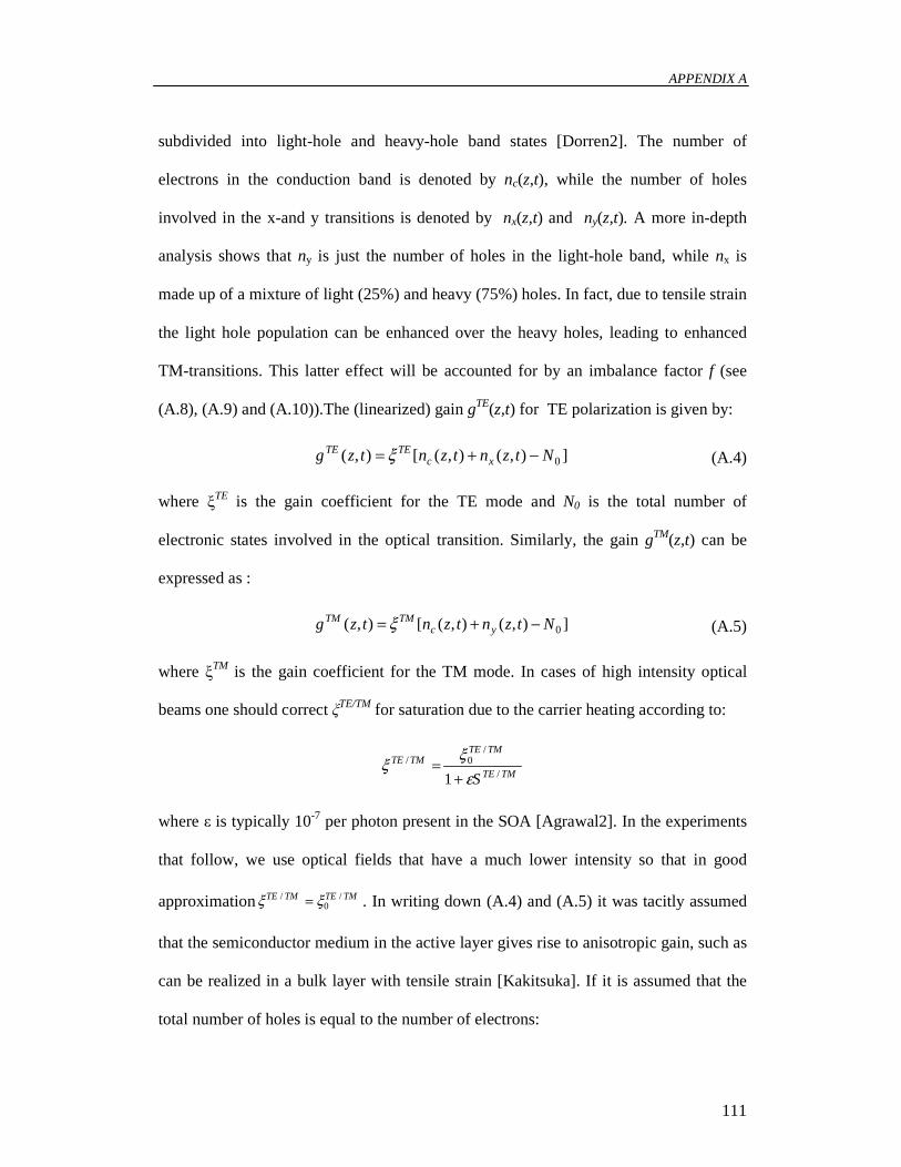
APPENDIX A
111
subdivided into light-hole and heavy-hole band states [Dorren2]. The number of
electrons in the conduction band is denoted by nc(z,t), while the number of holes
involved in the x-and y transitions is denoted by nx(z,t) and ny(z,t). A more in-depth
analysis shows that ny is just the number of holes in the light-hole band, while nx is
made up of a mixture of light (25%) and heavy (75%) holes. In fact, due to tensile strain
the light hole population can be enhanced over the heavy holes, leading to enhanced
TM-transitions. This latter effect will be accounted for by an imbalance factor f (see
(A.8), (A.9) and (A.10)).The (linearized) gain gTE(z,t) for TE polarization is given by:
]),(),([),( 0Ntzntzntzg xcTETE −+= ξ (A.4)
where ξTE is the gain coefficient for the TE mode and N0 is the total number of
electronic states involved in the optical transition. Similarly, the gain gTM(z,t) can be
expressed as :
]),(),([),( 0Ntzntzntzg ycTMTM −+= ξ (A.5)
where ξTM is the gain coefficient for the TM mode. In cases of high intensity optical
beams one should correct ξTE/TM for saturation due to the carrier heating according to:
TMTE
TMTETMTE
S /
/0/
1 εξξ
+=
where ε is typically 10-7 per photon present in the SOA [Agrawal2]. In the experiments
that follow, we use optical fields that have a much lower intensity so that in good
approximation TMTETMTE /0
/ ξξ = . In writing down (A.4) and (A.5) it was tacitly assumed
that the semiconductor medium in the active layer gives rise to anisotropic gain, such as
can be realized in a bulk layer with tensile strain [Kakitsuka]. If it is assumed that the
total number of holes is equal to the number of electrons:

MODEL FOR NONLINEAR POLARIZATION ROTATION
112
),(),(),( tzntzntzn yxc += (A.6)
and substitute this into (A.5) and (A.6), gTE (z,t) and gTM (z,t) can be expressed as :
]),(),(2[),(]),(),(2[),( 00 NtzntzntzgNtzntzntzg xyTMTM
yxTETE −+=−+= ξξ (A.7)
The rate-equation for nx(z,t) can be written as:
),(),(),(),(),(),(
21
tzStzgT
tzfntzn
T
ntzn
t
tzn TETEyxxxx −−
−−
−=∂
∂ (A.8)
and similarly for ny(z,t)
),(),(),(),(),(),(
21
tzStzgT
tzntzfn
T
ntzn
t
tznTMTMxyyyy −
−−
−−=
∂
∂ (A.9)
where xn and yn are the respective equilibrium values determined by the applied pump
current as will be discussed below, T1 is the electron-hole recombination time and T2 the
inter-hole relaxation time. The last terms in the right hand sides of (A.8) and (A.9)
account for the stimulated recombinations. It should be noted that the inter-hole
relaxation time T2 (~100 fs) is much shorter than the electron hole recombination time
T1 (~500 ps). Since it is not considered here applications that involve ultrafast
dynamics, the two populations nx and ny will be clamped tightly together i.e.
),(),( tzfntzn yx = (A.10)
In case of unstrained bulk material, the gain will be isotropic and f=1. In case of tensile
strain, TM gain will be larger than TE, i.e. f<1. For the equilibrium values it can be
written, consistent with (A.10):
f
nn
f
fnn yx +
=+
=11 (A.11)

APPENDIX A
113
where:
1Te
In = (A.12)
and I is the electric current and e is the electric unit charge. In (A.8)-( A.11) f expresses
the magnitude of the anisotropy.
The equations (A.1)-( A.12) form a closed set of equations. First it will be
calculated the small-signal gain. To this end, the equilibrium values (A.11) is
substituted in the gain expressions (7) and obtain the small signal gainTMTEg /
0 :
−
++=
−
++= 0000 )
1
2()
1
21( Nn
f
fgNn
f
fg TMTMTETE ξξ (A.13)
These expressions are quite general, but derived under the assumption of linear
relationship between gain and carrier numbers. This implies that (A.13) can only be
used in a small interval of the pump current. Within this given interval the parameter
values occurring in (A.13) can be determined, but for different intervals different
parameter values will be obtained.
According to (A.1) and (A.2) the net amplifications by the SOA (in dB), in absence
of spatial inhomogeneity, are given by:
TEg
TETETE
v
Lg )(343.4 intα−Γ× For TE (A.14)
and
TMg
TMTMTM
v
Lg )(343.4 intα−Γ× For TM (A.15)
where L is the length of the SOA. The small-signal amplification can be obtained by
replacing gTE by TEg0 and gTM by TMg 0 in (A.14) and (A.15).

MODEL FOR NONLINEAR POLARIZATION ROTATION
114
It should be noted that the SOA parameters N0, T1, ΓTE/TM, TMTE /intα , TMTE
gv / cannot be
estimated accurately. This problem is solved by compensating the combined
uncertainties in these parameter values by assigning values to f and ξTE/TM in such a way
that the (measured) fiber-to-fiber gain is reproduced. In the most simple approach, one
would choose ξTE = ξTM, as would be exact in the case of isotropic gain, so that f can be
estimated from the measured TE and TM gain curves by using (A.14) and (A.15). In
this case the polarisation dependent gain would be totally explained by the band filling
effects that are represented by the factor f. However, this leads to gain saturation that is
not in agreement with experimental data. It was therefore chosen to allow for a small
difference in the values for ξTE and ξTM (as could be due to a small difference in
effective transition strength). This approach leads to a gain saturation that is in good
agreement with experimental data. The difficulties in estimating f and ξTE/TM may be
inherent to our modelling the SOA strain in terms of a population imbalance factor f. In
a more accurate, but also much more complicated model, one can calculate the band
structure and transition matrix elements in the presence of tensile strain and keep track
of the different optical transitions involved as well as the relevant populations. This
would, however, extend beyond the scope of the present approach.


Appendix B
Characterization of the semiconductor optical amplifier
Nonlinear effects in a semiconductor optical amplifier (SOA), i.e. self-phase
modulation (SPM) or cross-gain modulation (XGM), have been used in this thesis to
achieve the presented optical signal processing functions. These nonlinear effects are
the results of nonlinear gain and index dynamics in the SOA. In this appendix, data are
presented about the SOAs used in the experiments. Firstly the SOA gain is shown as a
function of the wavelength. Afterwards, the SOA gain saturation is presented as a
function of the driving current, and as a function of the optical CW input power.
The strained bulk SOA (CQF872/0 # 459) was manufactured by JDS-Uniphase. The
characterizations of the fiber-to-fiber gain, saturation output power and gain ripple
versus wavelength have been done under the conditions reported in Table B.1 For this
specific SOA the operating temperature is between -15 and + 60 oC. The SOA reverse
voltage should be less than 2 V, while the SOA forward current should not exceed 600
mA. The length of the active region of the SOA was around 800 µm.
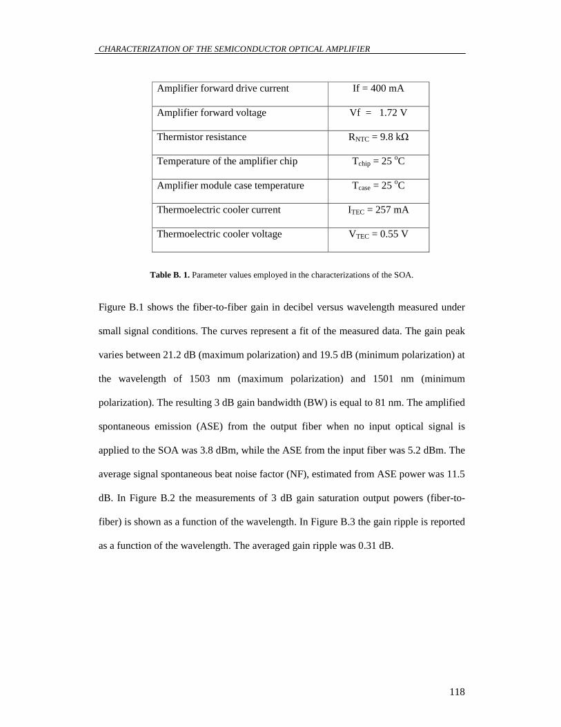
CHARACTERIZATION OF THE SEMICONDUCTOR OPTICAL AMPLIFIER
118
Amplifier forward drive current If = 400 mA
Amplifier forward voltage Vf = 1.72 V
Thermistor resistance RNTC = 9.8 kΩ
Temperature of the amplifier chip Tchip = 25 oC
Amplifier module case temperature Tcase = 25 oC
Thermoelectric cooler current ITEC = 257 mA
Thermoelectric cooler voltage VTEC = 0.55 V
Table B. 1. Parameter values employed in the characterizations of the SOA.
Figure B.1 shows the fiber-to-fiber gain in decibel versus wavelength measured under
small signal conditions. The curves represent a fit of the measured data. The gain peak
varies between 21.2 dB (maximum polarization) and 19.5 dB (minimum polarization) at
the wavelength of 1503 nm (maximum polarization) and 1501 nm (minimum
polarization). The resulting 3 dB gain bandwidth (BW) is equal to 81 nm. The amplified
spontaneous emission (ASE) from the output fiber when no input optical signal is
applied to the SOA was 3.8 dBm, while the ASE from the input fiber was 5.2 dBm. The
average signal spontaneous beat noise factor (NF), estimated from ASE power was 11.5
dB. In Figure B.2 the measurements of 3 dB gain saturation output powers (fiber-to-
fiber) is shown as a function of the wavelength. In Figure B.3 the gain ripple is reported
as a function of the wavelength. The averaged gain ripple was 0.31 dB.

APPENDIX B
119
Figure B.1 Fiber-to-Fiber gain versus wavelength.
Figure B.2 Saturation output power versus wavelength.
Figure B.3 Gain ripple versus wavelength.
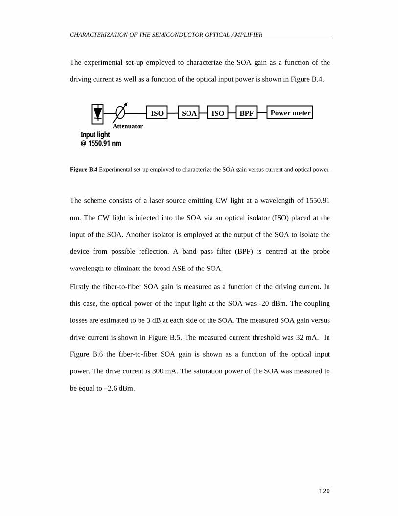
CHARACTERIZATION OF THE SEMICONDUCTOR OPTICAL AMPLIFIER
120
The experimental set-up employed to characterize the SOA gain as a function of the
driving current as well as a function of the optical input power is shown in Figure B.4.
Figure B.4 Experimental set-up employed to characterize the SOA gain versus current and optical power.
The scheme consists of a laser source emitting CW light at a wavelength of 1550.91
nm. The CW light is injected into the SOA via an optical isolator (ISO) placed at the
input of the SOA. Another isolator is employed at the output of the SOA to isolate the
device from possible reflection. A band pass filter (BPF) is centred at the probe
wavelength to eliminate the broad ASE of the SOA.
Firstly the fiber-to-fiber SOA gain is measured as a function of the driving current. In
this case, the optical power of the input light at the SOA was -20 dBm. The coupling
losses are estimated to be 3 dB at each side of the SOA. The measured SOA gain versus
drive current is shown in Figure B.5. The measured current threshold was 32 mA. In
Figure B.6 the fiber-to-fiber SOA gain is shown as a function of the optical input
power. The drive current is 300 mA. The saturation power of the SOA was measured to
be equal to –2.6 dBm.
Attenuator Input light @ 1550.91 nm
ISO SOA BPF Power meter ISO

APPENDIX B
121
Figure B.5 Measured SOA gain as a function of the drive current.
-20 -15 -10 -5 0 5 102
4
6
8
10
12
14
16
18
Gai
n [d
B]
Pinp [dBm]
Figure B.6 Measured SOA gain as a function of the optical power of the probe light.
0 50 100 150 200 250 300 350 400 -15
-10
-5
0
5
10
15
20
Fib
er-t
o-f
iber
Gai
n [d
B]
I [mA]

CHARACTERIZATION OF THE SEMICONDUCTOR OPTICAL AMPLIFIER
122
Figure B.5 and B.6 give an estimation of the gain change as a function of the drive
current and of the input optical power. To estimate also the phase changes associated
with the gain changes, the SOA parameters should also be characterized. Although
some parameters are wavelength and current dependent [Summers, Morthier,
Manning1], the typical values of a strained bulk SOA parameter are reported in Table
B.2 [Visser1, Visser2].
Electron hole recombination time 500 ps
Total number of electronic states N0=108
Group velocity for TE and TM modes vgTE= vg
TM=100µm/ps
Confinement factor for TE and TM ΓTE=0.2 ; ΓTM=0.14
Gain coefficient for the TE and the TM modes ξTE=7 10-9 ps-1; ξTM=6.5 10-9 ps-1
Modal losses αintTE= αint
TM=0.27 ps-1
Linewidth enhancement factor for TE and TM modes αTE= αTM=5
Table B.2 Typical parameters of a strained bulk semiconductor optical amplifier.


Appendix C
Description of the hexadecimal notation and Manchester code
In this appendix, a brief description of the hexadecimal notation and Manchester
encoding is given.
C.1 Hexadecimal notation
The most commonly used numbering system is the binary system. Binary digits (also
known as bits) are made entirely out of ‘0’s and ‘1’s. Each digit represents a power of 2
(also known as Base 2). If the number of digits (bits) required to represent a value (i.e. a
memory address) is large, hexadecimal notation can be used as a more compact way to
represent the same binary information. Each hexadecimal digit represents four binary
digits (a group of four binary is also known a nibble). Hexadecimal digits are 0 to 9 and
A to F. To convert between hexadecimal and binary digits, the following lookup table
can be used:

HEXADECIMAL NOTATION AND MANCHESTER CODE
126
0000 ↔ 0
0001 ↔ 1
0010 ↔ 2
0011 ↔ 3
0100 ↔ 4
0101 ↔ 5
0110 ↔ 6
0111 ↔ 7
1000 ↔ 8
1001 ↔ 9
1010 ↔ A
1011 ↔ B
1100 ↔ C
1101 ↔ D
1110 ↔ E
1111 ↔ F
Table C.1 Lookup table to convert hexadecimal to binary and binary to hexadecimal.
C.2 Manchester code
In telecommunications, Manchester encoding is a form of data communication in
which each bit of data is signified by at least one transition. Manchester encoding is
therefore considered to be self-clocking, which means that accurate synchronisation of a
data stream is possible. Each bit is transmitted over a predefined time period. Each
encoded bit contains a transition at the midpoint of a bit period (see Figure C.1).
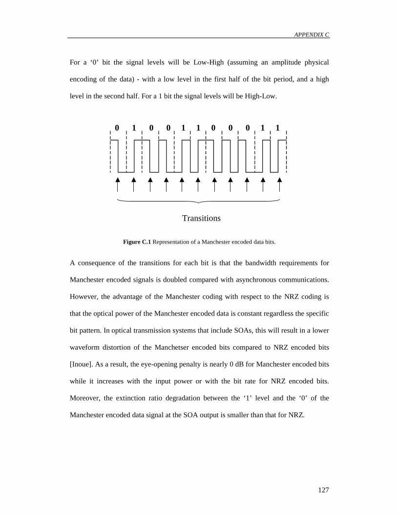
APPENDIX C
127
For a ‘0’ bit the signal levels will be Low-High (assuming an amplitude physical
encoding of the data) - with a low level in the first half of the bit period, and a high
level in the second half. For a 1 bit the signal levels will be High-Low.
Figure C.1 Representation of a Manchester encoded data bits.
A consequence of the transitions for each bit is that the bandwidth requirements for
Manchester encoded signals is doubled compared with asynchronous communications.
However, the advantage of the Manchester coding with respect to the NRZ coding is
that the optical power of the Manchester encoded data is constant regardless the specific
bit pattern. In optical transmission systems that include SOAs, this will result in a lower
waveform distortion of the Manchetser encoded bits compared to NRZ encoded bits
[Inoue]. As a result, the eye-opening penalty is nearly 0 dB for Manchester encoded bits
while it increases with the input power or with the bit rate for NRZ encoded bits.
Moreover, the extinction ratio degradation between the ‘1’ level and the ‘0’ of the
Manchester encoded data signal at the SOA output is smaller than that for NRZ.
0 1 0 0 1 1 0 0 0 1 1
Transitions


References
[Agrawal1] G. P. Agrawal and N. A. Olsson: “Self-phase modulation and spectral broadening of optical pulses in semiconductor laser amplifier,” IEEE Journal of Quantum Electronics, Vol. 25, pp. 2297-2306, 1989.
[Agrawal2] G.P. Agrawal, N.K. Dutta, “Long-wavelength semiconductor
lasers,” Van Nostrand Reinhold, New York, 1986. [Akiba] Shigeyuki Akiba, “The future of Optical communications,” IEEE
LEOS Newsletter, pp. 20-24, February 2003. [Bakhshi] B. Bakhshi, D. Kovsh, G. Mohs, R. Lynch, M. Manna, E.
Golovchenko, W. Patterson, M. Vaa, P. Corbett, M. Sanders, H. Li, G. Harvey, and S. Abbott, “Terabit/s field trial over the first installed dispersion-flattened transpacific system,” Optical Fiber Communication 2003, Post-deadline paper PD 27, Atlanta, USA, 2003.
[Bourouha] M. A. Bourouha, M. Bataineh, M. Guizani, “Advances in optical
switching and networking: past, present, and future,” IEEE SoutheastCon 2002, pp. 405-413, 2002.
[Calabretta1] N. Calabretta, Y. Liu, H. de Waardt, M.T. Hill, G.D. Khoe and
H.J.S. Dorren, “Multiple output all-optical header processing technique based on two pulse correlation principle,” Electronics Letters, Vol. 37, pp. 1238-1240, 2001.
[Calabretta2] N. Calabretta, Y. Liu, H. de Waardt, M. T. Hill, G. D. Khoe, and H.
J. S. Dorren, “Bragg grating assisted all-optical header pre-processor,” Electronics Letters, Vol. 38, pp. 1560-1561, 2002.
[Calabretta3] N. Calabretta, Y. Liu, H. de Waardt, M. T. Hill, G. D. Khoe, and H.
J. S. Dorren, “All-optical heder processor for all-optical packet networks’, IEE Proceeding-Optoelectronics, vol. 150, pp. 219-223, 2003.

REFERENCES
130
[Calabretta4] N. Calabretta, Y. Liu, F. M. Huijskens, M. T. Hill, H. de Waardt, G. D. Khoe, and H. J. S. Dorren, “Optical signal processing based on self-induced polarization rotation in a semiconductor optical amplifier,” IEEE Journal of Lightwave Technology, accepted for publication (February 2004).
[Calabretta5] N. Calabretta, Y. Liu, H. de Waardt, M.T. Hill, G.D. Khoe and
H.J.S. Dorren, “Ultrafast asynchronous multi-output all-optical header processor,” IEEE Photonic Technology Letters, accepted for publication (April 2004).
[Cardakli] M. C. Cardakli and A. E. Willner, “Synchronization of a network
element for optical packet switching using optical correlators and wavelength shifting,” IEEE Photonics Technology Letters, vol. 14, pp. 1375-1377, September 2002.
[Carena] A. Carena, M.D. Vaughn, R. Gaudino, M. Shell and D.J.
Blumenthal, “OPERA: An optical packet experimental routing architecture with label swapping capability,” Journal of Lightwave Technology, vol. 16, pp. 2135-2145, 1998.
[Charlet] G. Charlet, J.-C. Antona, S. Lanne, P. Tran, W. Idler, M. Gorlier, S.
Borne, A. Klekamp, C. Simonneau, L. Pierre, Y. Frignac, M. Molina, F. Beaumont, J.-P. Hamaide, S. Bigo, “6.4 Tb/s (159x42.7 Gb/s) capacity over 21x100 km using bandwidth-limited phase-shaped binary transmission,” European Conference on Optical Communication, ECOC 2002, Post-deadline paper PD 4.1, Copenhagen, Denmark, 2003
[Cottert1] D. Cotter, J. K. Lucek, M. Shabeer, K. Smith, D. C. Rogers, D.
Nesset and P. Gunning, “Self-routing of 100 Gbit/s packets using 6 bit ‘keyword’ address recognition,” Electronics Letters, vol. 31, pp. 2201-2203, 1995.
[Cotter2] D. Cotter and A. D. Ellis, “Asynchronous digital optical regeneration and networks,” IEEE Journal of Lightwave Technology, vol. 16, pp. 2068-2080, 1998.
[Deng] K.-L. Deng, I. Glesk, K. I. Kang, and P. R. Prucnal, “Umbalanced
TOAD for optical data and clock separation in self-clocked transparent OTDM networks,” IEEE Photonics Technology Letters, vol. 9, pp. 830-832, 1997.
[Dorren1] H. J. S. Dorren, M. T. Hill, Y. Liu, N. Calabretta, A. Srivatsa, F. M.
Huijskens, H. de Waardt and G. D. Khoe, “Optical packet switching and buffering by using all-optical signal processing methods,” IEEE Journal of Lightwave Technology, vol. 21, pp. 2-12, 2003.

REFERENCES
131
[Dorren2] H. J. S. Dorren, D. Lenstra, Y. Liu, M. T. Hill, and G. D. Khoe, “Nonlinear polarization rotation in semiconductor optical amplifiers: theory and application to all-optical flip-flop memories,” IEEE Journal of Quantum Electronics, vol. 39, pp. 141-147, 2003.
[Durhuus] T. Durhuus, B. Mikkelsen, C. Joergensen, S. L. Danielsen, and K. E.
Stubkjaer, “All-Optical Wavelength Conversion by Semiconductor Optical Amplifiers,” Journal of Lightwave Technology, vol. 14, pp. 942-954, 1996.
[Eiselt] M. Eiselt, W. Pieper, H.G. Weber, “SLALOM: Semiconductor Laser
Amplifier in Loop Mirror,” Journal of Lightwave Technology, vol. 13, pp. 2099-2112, 1995.
[Ellis] A.D. Ellis, A.E. Kelly, D. Nesset, D. Pitcher, D.G. Moody, and R.
Kashyap, “Error-free 100 Gbit/s wavelength conversion using grating assisted cross-gain modulation in 2 mm long semiconductor amplifier,” Electronics Letters, vol. 34, pp. 1958-1959, 1998.
[Garnot] M. Garnot, P. A. Perrier, “Planning of WDM networks: methods,
routing node modeling and applications,” Global Telecommunications Conference, 1998. GLOBECOM 98. The Bridge to Global Integration IEEE , vol. 1 ,pp. 351-355, 1998.
[Girardin] F. Girardin, G. Guekos, A. Houbavlis, “Gain recovery of bulk
semiconductor optical amplifier,” IEEE Photonics Technology Letters, vol. 10, pp. 784-786, 1998.
[Glesk1] I. Glesk, K.I. Kang, and P.R. Prucnal, “All-optical address
recognition and self-routing in a 250 Gbit/s packet switched,” Electronics Letters, vol. 30, pp. 1322-1323, 1994.
[Glesk2] I. Glesk, K.I. Kang, and P.R. Prucnal, “Demonstration of Ultrafast
all-optical packet routing,” Electronics Letters, vol. 33, pp. 794-795, 1997.
[Hill1] M.T. Hill, A. Srivatsa, N. Calabretta, Y. Liu, H. de Waardt, G.D.
Khoe, H.J.S. Dorren, “1×2 optical packet switch using all-optical header processing,” Electronics Letters, vol. 37, pp. 774-775, 2001.
[Hill2] M.T. Hill, “All-optical flip-flop based on coupled laser diodes,”
Microwave and optical technology letters, vol. 25, pp. 157-159, 2000.
[Hill3] M. T. Hill, H. de Waardt, G. D. Khoe and H. J. S. Dorren, “All-
optical Flip-flop Based on Coupled laser Diodes,” Journal of Quantum Electronics, vol. 37, pp. 405-413, 2001.

REFERENCES
132
[Hill4] Hill, M.T., H. de Waardt and H.J.S. Dorren, Fast all-optical flip-flop
using coupled Mach Zehnder Interferometers, CLEO 2001 Technical Digest, pp. 188, 2001.
[Hunter] D.K. Hunter, H.M. Nizam, M.C. Chia, I. Andonovic, K.M. Guild, A.
Tzanakaki, M.J. O’Mahony, J.D. Bainbridge, M.F.C. Stephens, R.V. Penty and I.H. White, “WASPNET, A wavelength switched packet network,” IEEE Communications Magazine, pp. 120-128, 1999.
[Inoue] K. Inoue, “Waveform distortion in a gain-saturated semiconductor
optical amplifier for NRZ and Manchester formats,” IEE Proc.-Optoelectronics, vol. 144, pp. 433-437, 1997.
[Kakitsuka] T. Kakitsuka, Y. Shibata, M. Itoh, Y. Kadota, Y. Tohmori, Y.
Yoshikuni, “Influence of buried structure on polarisation sensivity in strained bulk semiconductor optical amplifiers,” IEEE Journal of Quantum Electronics, vol. 38, pp. 85-91, 2002.
[Kawaguchi] H. Kawaguchi, “Bistable laserdiodes and their applications: State of
the art,” IEEE Journal of Selected Topics in Quantum Electronics, vol. 3, pp. 1254-1270, 1997.
[Keops] C. Guillemot et al, “Transparent Optical Packet Switching: The
European ACTS KEOPS Project Approach,” Journal of Lightwave Technology, vol. 16, pp. 2117-2134, 1998.
[Lee] Hyuek Jae Lee, Hae Genn Kim, Jee Yon Choi and Hak Kyu Lee,
“All-optical clock recovery from NRZ data with simple NRZ-to-PRZ converter based on self-phase modulation of semiconductor optical amplifier,” Electronics Letters, vol. 35, pp. 989-990, 1999.
[Liu1] Y. Liu, M. T. Hill, E. Tangdiongga, H. de Waardt, N. Calabretta, G.
D. Khoe, and H. J. S. Dorren, “Wavelength conversion using nonlinear polarization rotation in a single semiconductor optical amplifier,” IEEE Photonics Technology Letters, vol. 15, pp. 90-92, 2003.
[Liu2] Y. Liu, M. T. Hill, H. de Waardt, G. D. Khoe, D. Lenstra, and H. J.
S. Dorren, “All-optical flip-flop memory based on two coupled polarisation switches,” Electronics Letters, vol. 38, pp. 904-906, 2002.
[Liu3] Y. Liu, M. T. Hill, N. Calabretta, H. de Waardt, G. D. Khoe, and H.
J. S. Dorren, “All-optical buffering in all-optical packet switched cross-connects,” IEEE Photonics Technology Letters, vol. 14, pp. 849-851, 2002.
REFERENCES
133
[Manning] R. J. Manning , A. Antonopoulos, R. Le Roux and A. E. Kelly, “Experimental measurement of nonlinear polarization rotation in semiconductor optical amplifiers,” Electronics Letters, vol. 37, pp. 229-231, 2001
[Manning1] R. J. Manning, A. E. Kelly, A. J. Poustie, K. J. Blow, “Wavelength
dependence of switching constrast ratio of semiconductor optical amplifier-based nonlinear loop mirror,” Electronics Letters, vol. 34, pp. 916-918, 1998.
[Morthier] G. Morthier, P. Vankwikelberge, F. Buytaert, R. Baets, “Influence of
gain nonlinearities on the linewidth enhancement factor in semiconductor lasers,” IEE Proceedings-Optoelectronics, vol. 137, pp. 30-32, 1990.
[O’Mahony] M. J. O'Mahony, D. Simeonidou, D. K. Hunter, A. Tzanakaki, “The
application of optical packet switching in future communication networks,” IEEE Communications Magazine, vl. 39, Issue 3, pp. 128-135, 2001.
[Murata] M. Murata and Ken-ichi Kitayama, “Ultrafast photonic label switch
for asynchronous packets of variable length,” IEEE INFOCOM 2002, pp. 371-380, 2002.
[Patel] N. S. Patel, K. A. Rauschenbach, K. L. Hall, “40-Gb/s
demultiplexing using an ultrafast nonlinear interferometer (UNI),” IEEE Photonic Technology Letters, Vol. 8, pp. 1695-1697, 1996.
[Rau] L. Rau, S. Rangarajan, D.J. Blumenthal, H.-F. Chou, Y.-J. Chiu and
J.E. Bowers, “Two-hop all-optical label swapping with variable length 80 Gb/s packets and 10Gb/s labels using nonlinear fiber wavelength converters, unicast/multicast output and a single EAM for 80 – to 10Gb/s packet demultiplexing,” OFC 2002, Postdeadline papers, pp. FD2-1 FD2-3, 2002.
[Sakamoto] T. Sakamoto, A. Okada, M. Hirayama, Y. Sakai, O. Moriwaki, I.
Ogawa, R. Sato, K. Noguchi, and M. Matsuoka, “Demonstration of an optical packet synchronizer for an optical packet switch,” OFC 2002 Proceedings, pp. 762-763, 2002.
[Schreieck] R. Schreieck, M. Kwakernaak, H. Jackel, E. Gamper, E. Gini, W.
Vogt, H. Melchior, “Ultrafast switching dynamics of Mach-Zehnder interferometer switches,” IEEE Photonics Technology Letters, vol. 13, pp. 603 –605, 2001.
[Sokoloff] J. P. Sokoloff, P. R. Prucnal, I. Glesk, M. Kane, “A terahertz optical
asymmetric demultiplexer (TOAD),” IEEE Photonics Technology Letters, vol. 5, pp. 787 –790, 1993.

REFERENCES
134
[Sonet] http://www.sonet.com/ [Soto] H. Soto, D. Erasme, and G. Guekos, “5-Gbit/s XOR optical gate
based on cross-polarization modulation in semiconductor optical amplifier,” IEEE Photonics Technology Letters, vol. 13, pp. 335-337, 2001.
[Srivatsa] A. Srivatsa, H. de Waardt, M.T. Hill, G.D. Khoe and H.J.S. Dorren,
“All-optical serial header processing based on two-pulse correlation,” Electronics Letters, vol. 37, pp. 234-235, 2001.
[Stephens] M.F.C. Stephens, M. Asghari, R.V. Penty, and I.H. White, “Demonstration of ultrafast all-optical wavelength conversion utilizing birefringence in semiconductor optical amplifiers,” IEEE Photonics Technology Letters, vol. 9, pp. 449-451, 1997.
[Summers] H. D. Summers, I. H. White, “Measurement of the static and
dynamic linewidth enhancement factor in strained 1.55 mm InGaAsP lasers,” Electronics Letters, vol. 30, pp. 1140-1141, 1994.
[Visser1] T.D. Visser, H. Blok and D. Lenstra, “Theory of polarization
dependent amplification in a slab waveguide with anisotropic gain and losses,” IEEE Journal of Quantum Electronics, vol. 35, pp. 240-249, 1999.
[Visser2] T.D. Visser, H. Blok, B. Demeulenaere and D. Lenstra,
“Confinement factors and gain in optical amplifiers,” IEEE Journal of Quantum Electronics, vol. 33, pp. 1763-1766, 1997.
[Willner] A.E. Willner, D. Gurkan, A.B. Sahin, J.E. McGeehan, M.C. Hauer,
“All-optical address recognition for optically-assisted routing in next-generation optical networks,” IEEE Communication Magazine,vol. 41, pp. 38-S44, 2003.
[Wonglumsom] D. Wonglumsom, I. M. White, S. M. Gemelos, K. Shrikhande, and
L. G. Kazovsky, “HORNET – A packet-switched WDM network: Optical packet transmission and recovery,” IEEE Photonics Technology Letters, vol. 11, pp. 1692-1694, 1999.
[Xia] T. J. Xia, Y.-H. Kao, Y. Liang, J. W. Lou, K. H. Ahn, O. Boyraz, G.
A. Nowak, A. A. Said, and M. N. Islam, “Novel Self-Synchronization scheme for high-speed packet TDM networks,” IEEE Photonics Technology Letters, vol. 11, pp. 269-271, 1999.
[Zhao] M. Zhao, J. de Merlier, G. Morthier, and R. Baets, “Experimental
demonstration at 10 Gbps of 2R optical regeneration in a fiber-based MZI with LOAs,” ECOC Proceedings 2002, vol. 3, 7.3.6, Copenhagen, Denmark, 2002.

List of abbreviations
BPF Band Pass Filter
CSMA/CA Carrier Sense Multiple Access with Collision Avoidance
dB decibel
dBm decibel milliwatt
EDFA Erbium-doped Fiber Amplifier
FBG Fiber Bragg Grating
GaAs Gallium Arsene
HPP Header Pre-Processor
HPU Header Processing Unit
InP Indium Phoshide
IP Internet Protocol
LAN Local Area Network
MAN Metropolitan Area Network
MZI Mach-Zehnder Interferometer
NPS Nonlinear Polarization Switch
NRZ Nonreturn-to-Zero
OAF Optical Arbiter Function
OC Optical Circulator
OCDM Optical Code Division Multiplexer

LIST OF ABBREVIATIONS
136
OEO Optical-Electro-Optical
PBS Polarization Beam Splitter
PC Polarization Controller
PRBS Pseudo-Random Binary Sequence
RZ Return-to-Zero
SCM Sub-Carrier Multiplexer
SDH Synchronous Digital Hierarchy
SLALOM Semiconductor Laser Amplifier in a Loop Optical Mirror
SPM Self-Phase Modulation
SPR Self-induced Polarization Rotation
SOA Semiconductor Optical Amplifier
SONET Synchronous Optical Network
TDM Time-Division Multiplexing
TE Transverse Electric
TM Transverse Magnetic
TOAD Teraherz Optical Asynchronous Demultiplexer
UNI Ultrafast Nonlinear Interferometer
WDM Wavelength Division Multiplexing
XGM Cross-Gain Modulation
XPM Cross-Phase Modulation

List of publications
Journal papers
• N. Calabretta, Y. Liu, M. T. Hill, H. de Waardt, G. D. Khoe, and H. J. S.
Dorren, “Ultrafast asynchronous multi-output all-optical header processor,”
IEEE Journal Photonic Technology Letters, accepted for publication April
2004.
• N. Calabretta, Y. Liu, F. M. Huijskens, M. T. Hill, H. de Waardt, G. D. Khoe,
and H. J. S. Dorren, “Optical signal processing based on self-induced
polarization rotation in a semiconductor optical amplifier,” IEEE Journal of
Lightwave Technology, accepted for publication February 2004.
• N. Calabretta, Y. Liu, M. T. Hill, H. de Waardt, G. D. Khoe and H. J. S. Dorren,
“All-optical header processor for packet switched networks,” IEE Proceeding
Optoelectronics, vol. 150, no. 3, pp. 219-223, 2003.
• Y. Liu, M. T. Hill, E. Tangdiongga, H. de Waardt, N. Calabretta, G. D. Khoe
and H. J. S. Dorren, “Wavelength conversion using nonlinear polarization
rotation in a single semiconductor optical amplifier”, IEEE Photonics
Technology Letters, vol. 15, pp. 90-92, 2003.
LIST OF PUBBLICATIONS
138
• Y. Liu, M. T. Hill, N. Calabretta, H. de Waardt, G. D. Khoe and H. J. S.
Dorren, “Three state all-optical memory based on coupled ring laser”, IEEE
Photonics Technology Letters, vol. 15, pp. 1461-1463, 2003.
• H. J. S. Dorren, M. T. Hill, Y. Liu, N. Calabretta, A. Srivatsa, F. M. Huijskens,
H. de Waardt, G. D. Khoe, “Optical packet switching and buffering by using all
optical signal processing methods”, IEEE Journal of Lightwave Technology,
vol. 21, pp. 2-12, 2003.
• N. Calabretta, Y. Liu, H. de Waardt, G.D. Khoe and H.J.S. Dorren, “Bragg
grating assisted all-optical header pre-processor”, Electronics Letters, vol. 38,
pp.1560-1561, 2002.
• Y. Liu, M. T. Hill, N. Calabretta, H. de Waardt, G. D. Khoe and H. J. S. Dorren,
“All-optical buffering in all-optical packet switched cross connects”, IEEE
Photonics Technology Letters, vol. 14, pp. 849-851, 2002.
• N. Calabretta, Y. Liu, H. de Waardt, M. T. Hill, G. D. Khoe and H. J. S.
Dorren, “Multi-output all-optical header processing technique based on two-
pulse correlation principle”, Electronics Letters, Vol. 37, pp. 1238-1240, 2001.
• M. T. Hill, A. Srivatsa, N. Calabretta, Y. Liu, H. de Waardt, G. D. Khoe and H.
J. S. Dorren: ‘1x2 Optical Packet Switch using All-optic Header Processing’,
Electronics Letters, Vol. 37, pp. 774-775, 2001.
• E. Tangdiongga, N. Calabretta, P.C.W. Sommen, and H.J.S. Dorren “WDM
Monitoring Technique Using Adaptive Blind Signal Separation Theory”, IEEE
Photonic Technology Letters, Vol. 13, n. 3, March 2001.

LIST OF PUBBLICATIONS
139
International conferences
• N. Calabretta, Y. Liu, H. de Waardt, G.D. Khoe and H.J.S. Dorren, “Optical
Signal Processing based on Self-induced Polarization Rotation in a
Semiconductor Optical Amplifier”, ECOC 2003, Rimini, Italy, pp.178-179,
2003.
• N. Calabretta, Y. Liu, H. de Waardt, G.D. Khoe and H.J.S. Dorren, “All-optical
header-payload separator”, ECOC 2002, Copenhagen, Denmark, Mo. 1.4.4.,
2002.
• N. Calabretta, E. Tangdiongga, P.C.W. Sommen, and H.J.S. Dorren, “Signal
Reconstruction Technique for Monitoring WDM Channels”, ECOC 2001,
Amsterdam, The Netherlands, Mo. L.3.2., 2001.
Regional conferences
• N. Calabretta, M.T. Hill, Y. Liu, H. d. Waardt, G.D. Khoe and H.J.S. Dorren,
“All-optical header pre-processor based on self-phase modulation in a
semiconductor optical amplifier”, Proceedings Symposium IEEE/LEOS
Benelux Chapter 2002, 2002, Amsterdam, The Netherlands, pp. 99-102, 2002.\
• Y. Liu, M. T. Hill, N. Calabretta, H. de Waardt, G. D. Khoe, D. Lenstra and H.
J. S. Dorren, “All-optical flip-flop memory by using two coupled polarization
switches”, Proceedings Symposium IEEE/LEOS Benelux Chapter 2002,
Amsterdam, The Netherlands, pp. 199-202, 2002.
• N. Calabretta, M.T. Hill, Y. Liu, H. d. Waardt, G.D. Khoe and H.J.S.
Dorren,“Towards All-Optically Packet Switched Cross-Connect”, Proceedings
Symposium IEEE/LEOS Benelux Chapter 2001, 2001, Brussels, Belgium, 2001.

LIST OF PUBBLICATIONS
140
• E. Patent, J. J. G. van der Tol, N. Calabretta, Y. Liu “A pattern effect
compensator”, Proceedings Symposium IEEE/LEOS Benelux 2001, Brussels,
Belgium, 2001.
• N. Calabretta, M. T. Hill, G. Destura, Y. Liu, F. Huijskens, J. V. Bruni and H. J.
S. Dorren, “Photonic packet switching using all-optical header processing and
storage of header information”, Proceedings Symposium IEEE/LEOS Benelux
Chapter 2000, Delft, The Netherlands, pp. 199-202, 2000.
• J. V, Bruni, S. B. Colak, N. Calabretta, M. T. Hill, E. Tangdiongga, and H. J. S.
Dorren, “Adaptive photonic space-time coding and routing for wireless antenna
arrays”, Proceedings Symposium IEEE/LEOS Benelux Chapter 2000, Delft,
The Netherlands, pp. 51-54, 2000.

Sommario
Questa tesi tratta un riconoscitore (tutto) ottico di indirizzi. Il riconoscitore di indirizzi
e’ una delle funzioni fondamentali per lo sviluppo e l’implementazione di un
commutatore (tutto) ottico di pacchetti. Diversi approcci per l’implementazione di un
riconoscitore ottico di indirizzi sono riportati in letteratura, tuttavia in questa tesi si e’
considerato un approccio del riconoscitore ottico di indirizzi basato sulle nonlinearita’
del guadagno e le dinamiche dell’indice di rifrazione negli amplificatori ottici a
semiconduttore.
Dopo un’introduzione generale sull’argomento, il principio di operazione di un
commutatore ottico di pacchetti e’ discusso nel Capitolo 2. Il commutatore di pacchetti
consiste di un riconoscitore di indirizzi basato sul principio di two-pulse correlation in
un amplificatore ottico a semiconduttori posizionato in un loop ottico (SLALOM). Il
riconoscitore di indirizzi usato nel commutatore di pacchetti come presentato nel
Capitolo 2 puo’ riconoscere un solo specifico indirizzo. Nel Capitolo 3 si e’ dimostrato
che il principio di operazione del riconoscitore di indirizzi basato sul two-pulse
correlation puo’ essere generalizzato per riconoscere un maggior numero di indirizzi di
pacchetto.

SOMMARIO
142
Inoltre il commutatore di pacchetti presentato nel Capitolo 2 contiene una funzione
(tutto) ottica di soglia. Questa funzione di soglia e’ stata necessaria per aumentare il
contrasto tra l’impulso derivante dalla correlazione dell’indirizzo e il payload del
pacchetto. Per ovviare l’impiego delle funzioni di soglia (uno per ogni uscita del
riconoscitore di indirizzi) nel Capitolo 4 un pre-processore tutto ottico dell’indirizzo e’
stato dimostrato.
Nel Capitolo 5 un sistema di riconoscimento ottico dell’indirizzo basato su un pre-
processore (tutto) ottico dell’indirizzo e un riconoscitore di indirizzi e’ stato dimostrato
utilizzando effetti auto-indotti della rotazione nonlineare di polarizazione
nell’amplificatore ottico a semiconduttore. Il vantaggio di utilizzare un processore di
indirizzi e un pre-processore di indirizzi basati sulla rotazione nonlineare di
polarizzazione e’ che la potenza ottica di operazione utilizzata nel sistema di
processamento dell’indirizzo puo’ essere notevolmente ridotta rispetto al sistema
discusso nel Capitolo 4.
Infine, nel Capitolo 6 e’ stato dimostrato il principio di operazione di un riconoscitore
ottico di indirizzi basato sul terahertz optical asymmetric demultiplexer (TOAD). Il
vantaggio di utilizzare dei TOAD invece di SLALOMs consiste nel fatto che il
riconoscitore di indirizzi basato su TOADs puo’ essere integrato su chip. La
dimostrazione del riconoscitore di indirizzi basato su TOADs e’ presentata nel Capitolo
6. In contrasto con le altre tecniche di riconoscimento degli indirizzi basati sui TOADs,
il riconoscitore di indirizzi discusso in questa tesi opera in modo asincrono e quindi ha
il vantaggio di non richiedere il recupero del clock del segnale.

Acknowledgments
I would like to thank everybody who supported me in writing this thesis. In the first place the ones those are dearest to me, my girlfriend Suzanne and my families. Furthermore my promoter Djan Khoe who gave me the possibility to work and carry out research at the COBRA Institute. He encouraged me in conference and public talks by giving me the nickname of “Pavarotti”. Sure the comparison is too big! A lot of thanks to my supervisor Harm Dorren who believed in my work and led me towards the Ph.D. I am also grateful to my second promoter Daan Lenstra for supporting this work. I would like to thank my roommates for the nice time we spent together. Idelfonso Tafur for the interesting discussion and the very useful advises. Yong Liu with whom I discussed a lot about research objectives, laboratory experiences, courses and conferences. Thank you for all and ‘Nihao”. To Arvind Mishra, I wish “Shuprabhatam” for your ongoing Ph.D. Many thanks to Huug de Waardt and Martin Hill who were always willing to discuss results and to help in the laboratory. René Jonker especially for his useful discussions concerning my last paper. I am also grateful to Frans Huijskens who manufactured several components employed in my experiments, Peter van Bennekom for his support in the laboratory, and Ronelle Geldenhuys for commenting the English in the thesis. A kind thanks to Susan and Els both for their sympathy and for helping me out in the official matters. Hans Moerman for his patience in arranging a computer to write this thesis. Moreover, there are people who I wish to thank not only for the professional discussion but also for sharing their fun, Eduard Tangdiongga, Jarek Turkiewicz, Johan The Dubbliner van Zantvoort (unfortunately for him also my Beugelen mate), Daniel “Mucho trabajo” Baez Puche, J.J. Vegas Olmos, Erwin “hou doe” Verdurmen and Oscar “The Dancer” Diaz. I wish to thank also all the other members of the ECO and also OED group for their kindness, and I wish good luck to all the Ph.D. students. Moreover, SAS to Cosimo for the “lekker koffie” time, thanks to Ronald Broeke for his collaboration to arrange a joint experiment. Many thanks to all my friends in Italy and Netherlands who always support me. I would like to say to Djan Khoe, Daan Lenstra, Harm Dorren, Prof. Geert Morthier, Prof. Jørn Hvam, Prof. Meint Smit en Prof. Alfred Driessen that I am very grateful for all the time they invested in improving the quality of this thesis. Finally, I wish to thank Carola van Oudheusden for providing me her two beautiful works represented in the cover.


Curriculum vitae
Nicola Calabretta was born the 25th of September 1974 in Catanzaro, Italy. After his graduating at the Liceo Scientifico Statale in Soverato, he started his studies in Telecommunications Engineering at the Politecnico di Torino, Italy. He received his Bachelor degree in 1995, and his Master of Science degree in 1999. In 1999 he started his PhD at the faculty of Electrical Engineering, COBRA Research Institute, located at the Eindhoven University of Technology in Eindhoven. In 1995 he visited the RAI Research Center (Italian broadcasting television) in Turin. He designed an automatic procedure for designing and optimizing a 3 dB coupler at 2.5 GHz in microstrip technology for an antenna system. This work was included as a part of the Bachelor thesis. In 1999 he won a scholarship for the European exchanging program Erasmus that enabled him to carry out his master thesis at the faculty of Electrical Engineering at the Eindhoven University of Technology. There he investigated a novel cost-effective system for monitoring of WDM channels. He is currently acting as a referee for the IEEE Photonic Technology Letters.