albert-ludwigs-universitat¨ freiburg institut fur …ira.informatik.uni-freiburg.de ›...
TRANSCRIPT

ALBERT-LUDWIGS-UNIVERSITATFREIBURG
INSTITUT FUR INFORMATIKLehrstuhl fur Rechnerarchitektur
Prof. Dr. Bernd Becker
DIPLOMARBEIT
Simulation of Dynamic Effects ofResistive Open Defects
Alejandro Czutro(Student-ID 1133719)
Supervision: Dr. Ilia Polian
17th April 2007


Erklarung
Hiermit erklare ich, Alejandro Czutro, dass ich diese Ab-schlussarbeit selbstandig verfasst habe, keine anderen als dieangegebenen Quellen und Hilfsmittel verwendet habe, und dassich alle Stellen, die wortlich oder sinngemaß aus veroffentlichtenSchriften entnommen wurden, als solche kenntlich gemacht habe.Daruber hinaus erklare ich, dass diese Abschlussarbeit nicht,auch nicht auszugsweise, bereits fur eine andere Prufung ange-fertigt wurde.
Ort, Datum Unterschrift
3

4
Acknowledgements
I am grateful to Sandeep Gupta and Shahdad Irajpour ofUniversity of Southern California Los Angeles for providing deepinsight into the implementation of their gate delay fault simula-tor [19].
Many thanks to Dr. Ilia Polian for the supervision of my workduring the last six months; and to him and to Mr. Piet Engelkefor meticulous proofreading of the present manuscript.
Finally, I would like to thank my wife, Mrs. Kinga Czutro,for supporting me during the last four years of study, and forworking especially hard during the last six months, in order topermit me concentrate on this work and finish it on time.
Alejandro Czutro, Freiburg, 17th April 2007
5

6

Contents
1 Introduction 13
2 Preliminaries 192.1 Circuits . . . . . . . . . . . . . . . . . . . . . . . . . . . . . . 192.2 Basic principles of digital testing . . . . . . . . . . . . . . . . 26
2.2.1 Defects, faults and errors . . . . . . . . . . . . . . . . . 262.2.2 Test application . . . . . . . . . . . . . . . . . . . . . . 282.2.3 Fault coverage . . . . . . . . . . . . . . . . . . . . . . . 302.2.4 Simulation . . . . . . . . . . . . . . . . . . . . . . . . . 30
2.2.4.1 Logic simulation . . . . . . . . . . . . . . . . 302.2.4.2 Fault simulation . . . . . . . . . . . . . . . . 31
2.2.5 (Automatic) test pattern generation . . . . . . . . . . . 332.3 Delay fault modelling . . . . . . . . . . . . . . . . . . . . . . . 35
2.3.1 Test application . . . . . . . . . . . . . . . . . . . . . . 362.3.2 Application of two-pattern testing to sequential circuits 38
2.4 Fault coverage under resistive fault models . . . . . . . . . . . 41
3 Simulating Dynamic Effects of Resistive Opens 453.1 Overall structure of the RO-simulator . . . . . . . . . . . . . . 473.2 Application of RO-simulation to sequential circuits . . . . . . 50
4 More Preliminaries 514.1 Definitions and conventions . . . . . . . . . . . . . . . . . . . 51
4.1.1 Time issues and test application . . . . . . . . . . . . . 514.1.2 Input and output intervals . . . . . . . . . . . . . . . . 554.1.3 Delay model . . . . . . . . . . . . . . . . . . . . . . . . 57
4.2 Waveforms . . . . . . . . . . . . . . . . . . . . . . . . . . . . . 594.2.1 Initial definitions . . . . . . . . . . . . . . . . . . . . . 604.2.2 Intersection of waveforms . . . . . . . . . . . . . . . . . 61
7

8 CONTENTS
4.2.3 Translation of waveforms . . . . . . . . . . . . . . . . . 634.2.4 Inversion of waveforms . . . . . . . . . . . . . . . . . . 65
4.3 Signal descriptors . . . . . . . . . . . . . . . . . . . . . . . . . 664.3.1 Initial definitions . . . . . . . . . . . . . . . . . . . . . 664.3.2 cv-intervals and ncv-intervals . . . . . . . . . . . . . . 68
4.3.2.1 cv-intervals . . . . . . . . . . . . . . . . . . . 684.3.2.2 Intersection of description intervals . . . . . . 684.3.2.3 ncv-intervals . . . . . . . . . . . . . . . . . . 724.3.2.4 An example on cv- and ncv-intervals . . . . . 74
5 Delay Fault Simulation 755.1 Illustrative example . . . . . . . . . . . . . . . . . . . . . . . . 75
5.1.1 Fault-free simulation . . . . . . . . . . . . . . . . . . . 755.1.2 Faulty-circuit simulation . . . . . . . . . . . . . . . . . 775.1.3 Computing the detection set of delay size intervals . . . 79
5.2 The delay fault simulation algorithm . . . . . . . . . . . . . . 805.2.1 Fault-free simulation . . . . . . . . . . . . . . . . . . . 805.2.2 Faulty-circuit simulation . . . . . . . . . . . . . . . . . 825.2.3 Computing the detection set of delay size intervals . . . 87
6 Fault Coverage 936.1 Introduction . . . . . . . . . . . . . . . . . . . . . . . . . . . . 936.2 Fault coverage metrics for resistive opens . . . . . . . . . . . . 946.3 An example . . . . . . . . . . . . . . . . . . . . . . . . . . . . 956.4 Overall fault coverage . . . . . . . . . . . . . . . . . . . . . . . 97
7 Experimental Results 99
8 Conclusions 109
A Contents of the Attached CD-ROM 111

List of Figures
1.1 The RO-simulator . . . . . . . . . . . . . . . . . . . . . . . . . 16
2.1 Example combinational circuit . . . . . . . . . . . . . . . . . . 202.2 Example sequential circuit . . . . . . . . . . . . . . . . . . . . 202.3 Example sequential circuit, simplified representation . . . . . . 202.4 Example circuit . . . . . . . . . . . . . . . . . . . . . . . . . . 232.5 Defects, faults and errors . . . . . . . . . . . . . . . . . . . . . 272.6 Single and multiple stuck-at fault models . . . . . . . . . . . . 282.7 Test application . . . . . . . . . . . . . . . . . . . . . . . . . . 292.8 Example on fault simulation . . . . . . . . . . . . . . . . . . . 312.9 Algorithm: simple fault simulation . . . . . . . . . . . . . . . 322.10 Algorithm: deterministic TPG, overall procedure . . . . . . . 342.11 Detection of an LDF . . . . . . . . . . . . . . . . . . . . . . . 372.12 Scan design . . . . . . . . . . . . . . . . . . . . . . . . . . . . 39
3.1 Detection interval of an LDF . . . . . . . . . . . . . . . . . . . 463.2 Algorithm: overall proceeding of the RO-simulator . . . . . . . 48
4.1 Computing PLST: an example . . . . . . . . . . . . . . . . . . 534.2 Algorithm: computation of PLST . . . . . . . . . . . . . . . . 544.3 Example on input intervals of a single-input gate . . . . . . . 544.4 Example on input intervals of a multiple-input gate . . . . . . 564.5 Example on the application of the delay model . . . . . . . . . 584.6 Example on the application of the delay model . . . . . . . . . 594.7 Example: 0-intersection of waveforms . . . . . . . . . . . . . . 614.8 Example: 1-intersection of waveforms . . . . . . . . . . . . . . 624.9 Example: translation of waveforms . . . . . . . . . . . . . . . 644.10 Intersection of description intervals with the same logic value . 704.11 Intersection of description intervals with the same logic value . 714.12 Algorithm: computing the set of ncv-intervals . . . . . . . . . 73
9

10 LIST OF FIGURES
5.1 Simulation example: fault-free simulation . . . . . . . . . . . . 765.2 Simulation example: faulty-circuit simulation . . . . . . . . . . 795.3 Computing the output waveform of a NAND gate . . . . . . . 815.4 Computing the fault site’s signal descriptors . . . . . . . . . . 825.5 Computing the detection intervals of delay sizes . . . . . . . . 885.6 Computing the detection intervals of delay sizes . . . . . . . . 885.7 Computing the detection intervals of delay sizes . . . . . . . . 885.8 Computing the detection intervals of delay sizes . . . . . . . . 885.9 Computing the detection intervals of delay sizes . . . . . . . . 905.10 Computing the detection intervals of delay sizes . . . . . . . . 905.11 Computing the detection intervals of delay sizes . . . . . . . . 905.12 Computing the detection intervals of delay sizes . . . . . . . . 915.13 Computing the detection intervals of delay sizes . . . . . . . . 915.14 Computing the detection intervals of delay sizes . . . . . . . . 91
6.1 Example: computing fault coverage . . . . . . . . . . . . . . . 96
7.1 Use of resources depending on number of faults . . . . . . . . 1047.2 Use of resources depending on depth of circuit . . . . . . . . . 1047.3 Fault coverage depending on number of faults . . . . . . . . . 1057.4 Fault coverage depending on depth of circuit . . . . . . . . . . 1057.5 FC depending on number of test pairs, circuit c5315 . . . . . . 1067.6 FC depending on number of test pairs, circuit s35932 . . . . . 106

List of Tables
2.1 Types of gates and their parameters . . . . . . . . . . . . . . . 24
4.1 Delay model . . . . . . . . . . . . . . . . . . . . . . . . . . . . 58
5.1 Rules for the creation of output description intervals . . . . . 85
7.1 Rising and falling delay times of each gate type . . . . . . . . 1007.2 Experimental results: tabular overview . . . . . . . . . . . . . 1027.3 Experimental results: tabular overview . . . . . . . . . . . . . 103
11

12 LIST OF TABLES
1
Introduction
Nowadays, electronics belong to modern life more than ever before. Theautomotive industry is only one example of an area which cannot do with-out integrated circuit (IC) technology any more. At the same time, as theareas in which IC technology is necessary, expand steadily, the complex-ity of digital systems rises constantly. This, together with increased deviceoperation speed and component miniaturisation as a response to the attemptof achieving higher performances, has as consequence that it is practicallyimpossible to guarantee that a digital IC is defect-free.
Since a defective IC placed onto a printed circuit board usually makesthe whole board and all other (possibly fault-free) components on it useless,the costs of shipping a defective IC may exceed the profit margin by far [34].Due to this fact, the correct function of all delivered ICs must be verifiedby testing after they have been manufactured. Testing represents the singlelargest manufacturing expense in the semiconductor industry, costing over$40 billion a year (by 2003, [21]).
The general strategy consists in applying a set of input vectors to the cir-cuit under test (CUT) and verifying if its outputs are as expected. However,digital testing comprises many more tasks, which are steadily being improvedin order to: 1) meet the requirement of testing constantly more and morecomplex becoming ICs; 2) reduce the costs of testing. The two most impor-tant tasks are test pattern generation (TPG) and fault simulation.
TPG is the task of generating a set of input vectors (called test patterns)to be applied to the CUT. A set of test patterns is called test set. A testpattern p is said to detect a fault f , if the response of the fault-free circuitdiffers from the response of the circuit with the fault f , when p is applied tothe circuit’s inputs. A test set is said to detect a fault if at least one of thetest patterns in the test set detects the fault. The effectiveness of TPG is
13

14 1. INTRODUCTION
measured by the percentage of faults that are detected (covered) by applyingthe generated test set. This measure of the quality of the test set is calledfault coverage.
Fault simulation is the process of determining the set of faults which aredetected by applying a test set to a circuit. Fault simulation is necessary tomeasure fault coverage without having to apply the generated test set to anactual circuit. Fault simulation is also a very important part of the overallTPG process, which usually consists of several phases. The goal of eachphase depends on the fault coverage achieved by the result of the precedingphase. Fault simulation of a test pattern p for a fault f consists of fault-freesimulation followed by faulty-circuit simulation. Fault-free simulation is theprocess of determining the steady state of the fault-free CUT after applyingp to its inputs. Faulty-circuit simulation determines the steady state of theCUT when it is affected by f after applying p to its inputs. The resultsof fault-free and faulty-circuit simulation are compared. If these differ, f isdetected by p.
Among the typical defects encountered in today VLSI chips are missingor broken contacts, opens (broken lines), shorts and bridges (unintendedcontacts), contacts with too low conductance, surface impurities, etc. Someaffect the functional behaviour of the circuit (i.e. cause the circuit to producea wrong output or to produce an output which cannot be interpreted as avalid logical value), some affect its timing behaviour (i.e the circuit producesthe right outputs, but these arrive too late), some do both, and others havefurther effects which do not need to be mentioned here. As it is not possibleto list all defects that may occur in a circuit, so-called fault models are usedto describe the faulty behaviour of a circuit having one or several defects.
The most popular fault model used in practice is the single stuck-at faultmodel [10], [14], [34, p. 16], [21]. Under this fault model, a single line in thecircuit is assumed to be affected. That line has always a fixed logic value,regardless of what inputs are supplied to the circuit. Despite the assumptionthat only one single line can be affected, working under the stuck-at faultmodel detects a large amount of complex defects which are usually modelledby other fault models.
Due to the increased interconnection density of today’s circuits, defectsthat affect the interconnect are becoming very frequent. Among these areopens and bridges, where opens constitute the major part of those defectswhich remain undetected during the test phase [32].
Traditionally, open defects were defined as unconnected nodes in themanufactured circuit that were connected in the original design. However,

15
open defects can also still connect the nodes, but only weakly, by introduc-ing between the linked points a resistance that is higher than expected butfinite [17], [32]. In [43], opens are classified into strong and weak ones.Strong opens are those with a very high resistance (more than 10 MΩ)and are thus treated as fully broken connections. These defects result in amemory behaviour at the fault site [45]. They can be modelled as stuck-open, stuck-on, or even stuck-at faults. In the past, strong opens have beenstudied extensively [37], [17], [7], [22].
Weak or resistive opens (i.e. opens with a low or moderate resistance lessthan 10 MΩ) manifest themselves as lines with an elevated resistance or asresistive vias and contacts. They still let the circuit work, but increase thedelay of paths (sequences of lines connected by gates) going through the faultsite [25], [29]. Not all these defects can be modelled effectively by the stuck-atfault model [2], [9], [8]. Thus, they are modelled by delay fault models whichassume that one single gate or path is slow to propagate 0 → 1 or 1 → 0transitions, delaying them by an additional unknown amount of time. Hence,resistive opens require a delay testing strategy. Delay testing strategies arecharacterised by the application of two successive test patterns (a test pair).The first test pattern brings the circuit into a known and stable state. Thesecond pattern changes the state of the circuit. If the circuit’s stabilisationafter the state change takes place after a certain threshold time, the delayfault is detected. [43] shows that in modern deep sub-micron technology, thepercentage of weak opens is high enough to require delay fault testing.
The amount of time by which the transitions are delayed is called thesize of the delay fault. It depends on the open’s resistance, which is anunpredictable random parameter [41]. A resistive open may be detected bya pair of test patterns if it has a certain resistance, while the same pair mightnot detect an open at the same location if the open has a different resistance.Since the resistance of an open in an actual manufactured circuit cannot beknown a priori, it is necessary to generate more than one pair of test patternsto detect the open. Enlarging the range of resistances for which the open isdetected is equivalent to increasing the probability that the open is detectedif it is present.
The aim of this work was to design and implement a simulator which isable to compute, for each delay fault in a given fault list, a set of resistanceranges, for which the resistive open modelled by the fault is detected by agiven test set. That set of resistance ranges is called the C-ADI (“Covered-Analogous Detection Interval”, [40]) of the fault. Furthermore, the simulatorshould be able to compute the fault coverage the given test set achieves. The
16 1. INTRODUCTION
Delay−to−resistancemapping
Computationof fault
coverage
Delay
fault
simulation
RO−SIMULATOR
C−ADI
FC
Circuit
Fault list
Test set
CDSI
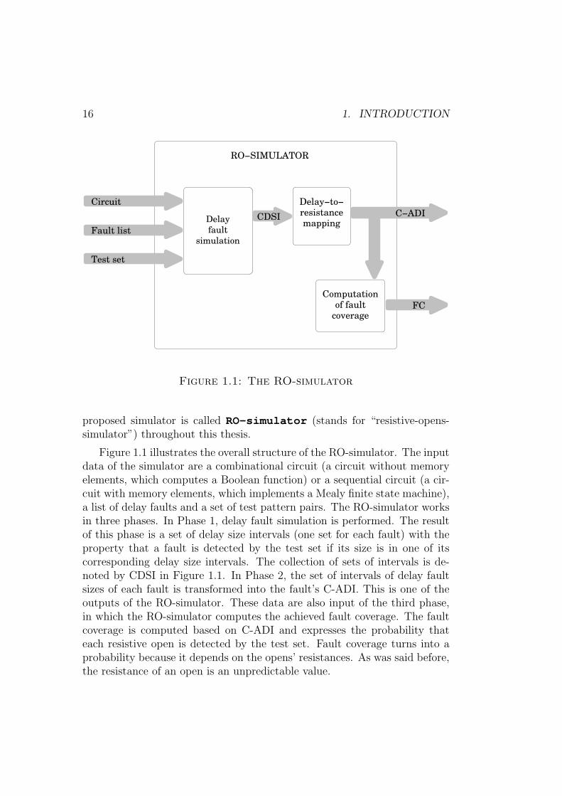
Figure 1.1: The RO-simulator
proposed simulator is called RO-simulator (stands for “resistive-opens-simulator”) throughout this thesis.
Figure 1.1 illustrates the overall structure of the RO-simulator. The inputdata of the simulator are a combinational circuit (a circuit without memoryelements, which computes a Boolean function) or a sequential circuit (a cir-cuit with memory elements, which implements a Mealy finite state machine),a list of delay faults and a set of test pattern pairs. The RO-simulator worksin three phases. In Phase 1, delay fault simulation is performed. The resultof this phase is a set of delay size intervals (one set for each fault) with theproperty that a fault is detected by the test set if its size is in one of itscorresponding delay size intervals. The collection of sets of intervals is de-noted by CDSI in Figure 1.1. In Phase 2, the set of intervals of delay faultsizes of each fault is transformed into the fault’s C-ADI. This is one of theoutputs of the RO-simulator. These data are also input of the third phase,in which the RO-simulator computes the achieved fault coverage. The faultcoverage is computed based on C-ADI and expresses the probability thateach resistive open is detected by the test set. Fault coverage turns into aprobability because it depends on the opens’ resistances. As was said before,the resistance of an open is an unpredictable value.

17
The implementation of Phase 1 of the RO-simulator is based on the delayfault simulation method RTM (“Ranges-type testing methodology”) by Pra-manick and Reddy [36]. That simulation method is called PR-simulator(“Pramanick-Reddy-simulator”) in this thesis. The PR-simulator is an ex-tension of a method introduced in [20], and is extended itself by Irajpour,Gupta and Breuer in [19]. In the RO-simulator’s Phase 1, the PR-simulator’stechniques for the description of dynamic behaviour of signals and for thepropagation of fault effects through the circuit have been improved by cal-culating the cumulative fault effect of all inputs of a logic gate rather thanconsidering all inputs explicitly. A further improvement of the PR-simulator,which was designed for combinational circuits, permits the RO-simulator tobe also used on sequential circuits.
In Phase 2, the RO-simulator converts the set of delay size intervals ofeach fault into its C-ADI. The base for this conversion is a delay-to-resistancemapping δ 7→ r with the meaning that a resistive open with resistance rproduces a delay fault of size δ. In this first implementation of the simulator,a trivial delay-to-resistance mapping is used. This mapping assumes that theadditional line delay caused by an open is linearly proportional to the open’sresistance. Physically accurate mappings, such as one introduced in [24], canbe easily integrated into the RO-simulator.
In Phase 3, the RO-simulator computes the fault coverage the given testset achieves. In order to do this, existing fault coverage metrics for resistivebridging faults [40], [38], [39], [23], [11], [12], [13] were adapted to the case ofresistive opens.
This first implementation of the RO-simulator was tested on ISCAS 85and ISCAS 89 circuits. Results are reported and analysed in this thesis.
The thesis is organised as follows. The next chapter introduces someconventions for this work and the basics on testing digital ICs. In Chapter 3the requirements the RO-simulator must meet are formulated in a formal way,and the RO-simulator’s overall structure is presented. Chapter 4 introducessome definitions which are necessary to understand Chapter 5, in which thealgorithms of Phase 1 are presented in detail and illustrated by means ofexamples. In Chapter 6 fault coverage metrics are discussed. Experimentalresults are reported in Chapter 7. Chapter 8 concludes the work.

18 1. INTRODUCTION
2
Preliminaries
While there is a wide variety of text books providing a good introductioninto the area of testing digital ICs ([1], [21] and [4] are only a few examples),this chapter has been composed in order to introduce the basic concepts ontesting which are needed to understand the present thesis. Additionally, theterminology used in all the other chapters is introduced.
Since digital testing is a discipline with a strong connection to thepractice, new research topics typically emerge after new problems occur de-pending on the technology development. Much of the conducted researchdoes not constitute a fundamental breakthrough. Instead, existingmethods are gradually improved [34, Chapter 2]. That is also thecharacteristic of the work presented in this thesis. The RO-simulator com-bines several already existing techniques, while the original work consists inmodifying those techniques to improve performance and to allow them towork together. The second purpose of this chapter is to help to distinguishbetween original work and those results obtained by other authors in thepast. No result which can be found in this chapter has been obtained byourselves. In all other chapters, non-original results are still referenced.
2.1 Circuits
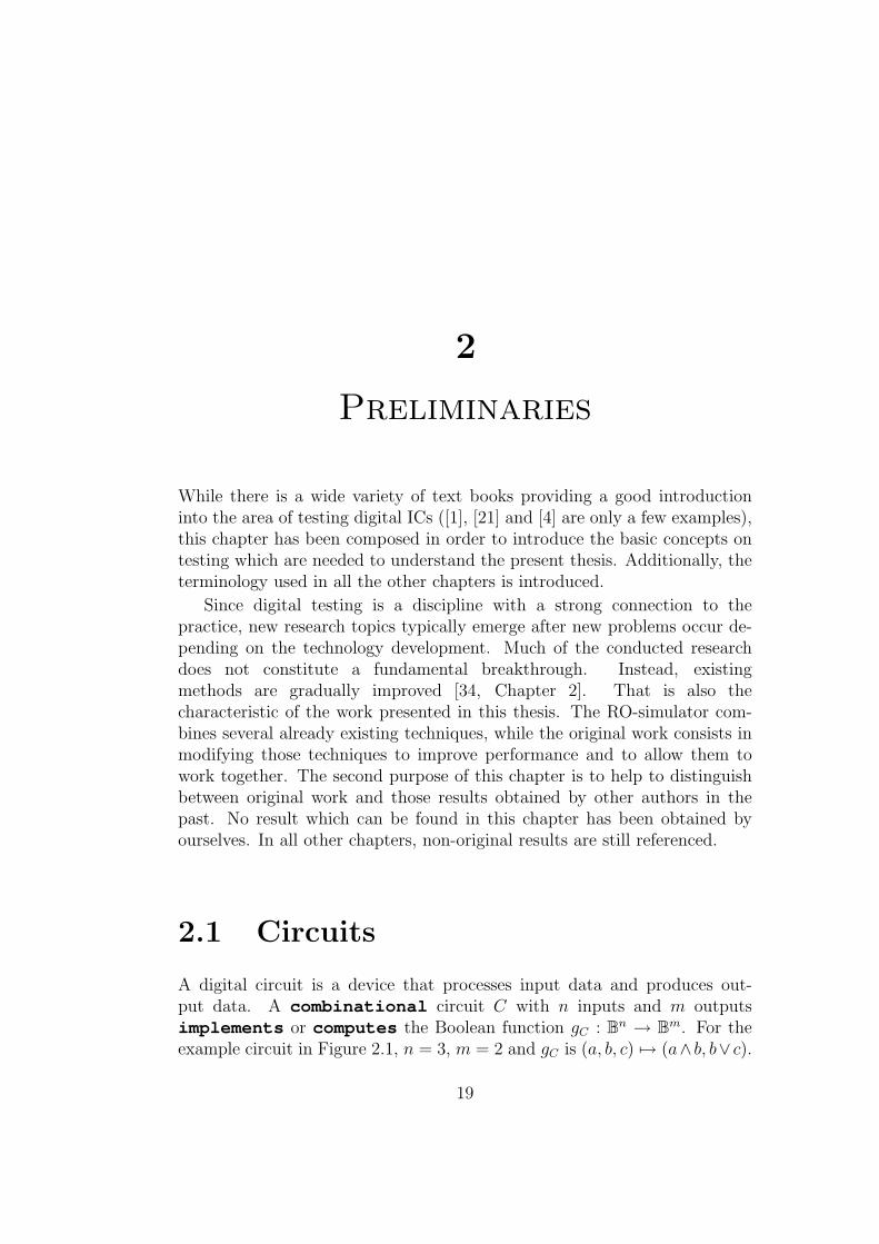
A digital circuit is a device that processes input data and produces out-put data. A combinational circuit C with n inputs and m outputsimplements or computes the Boolean function gC : Bn → Bm. For theexample circuit in Figure 2.1, n = 3, m = 2 and gC is (a, b, c) 7→ (a∧ b, b∨ c).
19

20 2. PRELIMINARIES
b
c
a
Figure 2.1: Example combinational circuit
D−FF
b
a
c
c’
d
clock
Figure 2.2: Example sequential circuit
a
b
c
c’
d
Figure 2.3: Example sequential circuit, simplified representa-tion

2.1 CIRCUITS 21
Circuits which contain memory elements are called sequential . Figure2.2 pictures an example sequential circuit. The box with the inscription“D-FF” is a D-flip-flop, a very common type of memory element.
Memory elements in sequential circuits are clocked, that means they areconnected to a device which generates a clock signal . The clock signaloscillates between logic 1 and logic 0, normally with a 50% duty cycle (i.e. itproduces a square waveform), and is used to synchronise the actions of allmemory elements. These are designed such that they can store a new valueonly while the clock is high (or only when the clock is low, depending onthe implementation). A clock cycle is composed of one falling (a 1 → 0transition) and one rising edge (a 0 → 1 transition) of the clock and itslength is called clock period or clock sampling time . This lengthis denoted by TC. In normal operation mode, new input vectors are appliedto the sequential circuit once every clock cycle. A clock cycle is also called atime frame .
A sequential circuit C with n inputs, m outputs and k flip-flops can beregarded as implementation of a Mealy finite state machine with 2k or lessstates. The states are encoded by the data stored in the flip-flops, whilethe combinational logic of the circuit (inside the dashed box in the example)computes the output function gC : Bn×Bk → Bm and the transition functionδC : Bn×Bk → Bk, which depend both on the inputs and on the present state.The gC-values are sent to the outputs and the δC-values are stored back intothe flip-flops. In the current example, n = 2, m = 1 and k = 1. Further,the machine has two states, 0 and 1, encoded by c. gC maps
((a, b), (c)
)to
(a ∧ c) and δC maps((a, b), (c)
)to (c ∨ b).
For some testing tasks, it is often convenient to ignore the memory ele-ments and to only consider the sequential circuit’s combinational core. Theoutputs of memory elements (e.g. c in Figures 2.2 and 2.3) are treated asadditional inputs to the combinational core. These are called secondaryinputs . The inputs of memory elements (e.g. c′) are treated as additionaloutputs of the combinational core. These are called secondary outputs .Regular inputs and outputs (a, b and d) are then called primary inputsand primary outputs , respectively. Instead of handling the output func-tion gC and the transition function δC separately, only one global functiongS : Bn+k → Bm+k, which is computed by the combinational core, needs tobe considered. In the current example, gS maps (a, b, c) to (a ∧ c, c ∨ b).
Each secondary input corresponds to exactly one secondary output,namely to the secondary output which feeds its source memory element.In a time frame i, the values of the secondary inputs are the values of theircorresponding secondary outputs in time frame i− 1.

22 2. PRELIMINARIES
When simulating sequential circuits, the first time frame needs specialtreatment, as only the primary inputs and outputs are accessible from theoutside of the circuit. There are techniques that make secondary inputspartially or fully accessible during test application, but these techniques havesome drawbacks (see Section 2.3.2).
When secondary inputs and outputs are not accessible from the out-side of the circuit, it is necessary to bring the circuit to a known state(i.e. to cause known values to be stored into the memory elements) beforeperforming simulation. If the hardware implements a reset function, resettingthe hardware will bring it to a known state. If no hardware reset is possible,one can try to find a so-called synchronising or homing sequence. Inthe example, the input (1, 1) can be applied to the primary inputs of the cir-cuit while the secondary input c has a defined but unknown value. Then, thevalue of the secondary output c′ is 1, as OR gates always produce the output1 if at least one of their inputs has the logic value 1. In the next time frame,a logic 1 is stored in the flip-flop. Altogether, applying the sequence (in thisexample, of length 1) of input vectors (1, 1) brings the machine to a knownstate. Thus, (1, 1) is a synchronising sequence. However, this technique isnot infallible as it is not always possible to find such a sequence. Readingfrom a secondary output is possible using a similar technique. Suppose thatthe secondary output c′ has the value 1 in time frame i. If the input (1, 0) isapplied to the primary inputs in time frame i + 1, the value of the primaryoutput d is 1 in time frame i + 1. Analogously, if the value of c′ is 0 in timeframe i, the value of d is 0 in time frame i + 1. Thus, in order to read thesecondary output c′, it suffices to apply the input (1, 0) to the primary inputsand to observe the primary output d in the following time frame.
Applying synchronising sequences requires simulating one or several timeframes until all flip-flops have a known logic value. During those time frames,at least one flip-flop will have a defined but unknown logic value, which mustbe propagated through the combinational core. In order to make simulationpossible, a three-valued algebra can be used. That algebra consists of logic1, logic 0 and the logic value X . X stands for a defined but unknownlogic value. 0 and 1 are then called determinate values.
This section is finalised with a list of conventions which are observedthroughout this work. Figure 2.4 shows how circuits are represented graphi-cally in this thesis and the following list introduces terminology used in thedescription of algorithms.

2.1 CIRCUITS 23
5 / 7
3
7 / 5
2
3 / 2
5
2 / 3
4
4 / 6
6 / 4
7
6
P_IN AND BUF OR P_OUT
S_IN NAND INV NOR S_OUT cell 4
0
1
8
9
FD(3) = 7 RD(7)=6
Figure 2.4: Example circuit
• The implemented simulator uses a three-valued algebra consisting ofthe values 0, 1 and X. X stands for a defined but unknown value.Let v be a logic value. Then, v denotes the logic inversion of v. 0 = 1,1 = 0 and X = X.
• Logic gates and primary and secondary input and output pins are calledcells . Each cell in the circuit is identified uniquely by an integerbetween 0 and k − 1, where k is the number of cells in the circuit.Cells are ordered topologically, i.e. secondary and primary inputs areassigned the identification numbers 0 through n − 1, where n is thenumber of primary and secondary inputs in the circuit. Every othercell is assigned an identification number which is greater than thoseof its predecessors. That means, whenever it is necessary to performan algorithm on all cells in the circuit, the algorithm starts with cell 0and ends with cell k − 1. When processing any cell i, its inputs havealready been processed.
• Input pins are also simply called inputs, output pins outputs.
• Each cell not being an input or an output is called a gate and is of

24 2. PRELIMINARIES
type INV, BUF, AND, OR, NAND, or NOR. A gate of type INV is aninverter, a gate with one input which computes the Boolean negation.A gate of type BUF is a buffer, a gate with one input which computesthe identity function. Gates of type AND, NAND, OR or NOR haveall at least two inputs. AND gates compute the Boolean conjunction,NAND gates the negation of the Boolean conjunction, OR gates theBoolean disjunction, and NOR gates the negation of the Boolean dis-junction. All gates have exactly one output.
All algorithms in this work only distinguish between single-inputand multiple-input gates. The behaviour of all single-input gatescan be described depending on only one parameter called inversion .If a single-input gate is inverting, it produces the output v if its input isv. If the gate is not inverting it produces the output v if its input is v.Analogously, the behaviour of all multiple-input gates depends on threeparameters called inversion , controlling value (abbreviatedCV(c) for a gate c) and non-controlling value (abbreviatedNCV(c)). If at least one input of a multiple-input gate c has thelogic value CV (c), then c produces the output value CV (c) (NCV (c)if c is inverting), no matter what logic values the other inputs have.In contrast, c can only produce the output NCV (c) (CV (c) if c isinverting) if all its inputs have the logic value NCV (c) at the sametime.
gate type inverting cv ncv
single-input gatesBUF no - -
INV yes - -
multiple-input gates
AND no 0 1
NAND yes 0 1
OR no 1 0
NOR yes 1 0
Table 2.1: Types of gates and their parameters
Gates of type XOR are not treated in this work, as the rules explainedabove do not apply to them. Note that an XOR gate can be replaced

2.1 CIRCUITS 25
by several gates of the above types, as a XOR b =((a ∧ b) ∨ (a ∧ b)
)for all logic values a and b.
• In all graphical representations of circuits, gates are shown togetherwith two numbers separated by a slash. For instance, those two num-bers are 5 and 7 for gate 3 in the example. The first is the number oftime units the gate needs to switch from 0 to 1 (produce a risingtransition ); this number is called rising delay time of c fora gate c and abbreviated by RD(c). The second is the number of timeunits the gate needs to switch from 1 to 0 (produce a fallingtransition ); this number is called falling delay time of c fora gate c and abbreviated by FD(c).
• Instead of distinguishing between lines and their corresponding logicsignals, lines are also simply called signals . Like cells, signals areidentified uniquely by an integer between 0 and l − 1, where l is thenumber of signals in the circuit. For all i = 0, . . . , l−1, the identificationnumber of the output signal of cell i is also i. This identification systemfor signals is well-defined as each signal has exactly one source cell andall gates and all input pins have exactly one output signal.
• Fanout stems are not discerned from fanout branches. A stem and allits branches are represented by only one common signal. (Example:signals 0, 1, 4 and 5 in Figure 2.4.)
• A signal which is the output of a primary input pin is also called aprimary input, a signal which is the output of a secondary input pinalso a secondary input, a signal which is the input of a primary outputpin also a primary output and a signal which is the input of a secondaryoutput pin also a secondary output.
• Let s be a signal and let c be its source cell. Then, the input signalsof c are called predecessor signals of s. For example, signals 4and 5 are predecessors of signal 7 in Figure 2.4.
• Let s be a signal and let c1, c2, . . . , cr be its drain cells. Then, theset containing the output signal of c1, the output signal of c2, . . . andthe output signal of cr is called set of successor signals of s. Forexample, signals 2 and 3 are successors of signal 0 in Figure 2.4.
• Let s1 and s2 be signals. A path from s1 to s2 is the sequence ofsignals starting with s1 and ending with s2, where each signal in the

26 2. PRELIMINARIES
sequence is a successor signal of the previous signal in the sequence.For example, the path from signal 0 to signal 7 in Figure 2.4 is thesequence of signals 0, 2, 4 and 7.
• Let s be a signal. The output cone of s is the set containing allsignals of every path between s and any primary or secondary output.s is not in its own output cone. For example, the output cone of signal2 in Figure 2.4 is composed of signals 4, 6 and 7.
2.2 Basic principles of digital testing
2.2.1 Defects, faults and errors
In engineering, models bridge the gap between physical reality and mathe-matical abstraction. They are essential in the areas of design and test asthey allow the development and application of analytical tools.
When testing digital ICs, it is necessary to understand the differencebetween defects , faults and errors . A defect is the unintended dif-ference between the implemented hardware and its intended design. Notethat not design mistakes are meant, but defects which come into existenceduring the manufacturing process. Some typical defects in VLSI chips aremissing or broken contacts, shorts, contacts with too low conductance, sur-face impurities, etc. A fault is a formal representation of the defect. Thewrong response of a defective system is an error. For example, Figure 2.5pictures an AND gate whose input b is shorted to ground. This is the defectof the system. It can be represented by the fault b stuck-at-0, which meansthat signal b always has the logic value 0, independently of what value isproduced by b’s source cell. An error occurs if the input (1, 1) is applied tothe gate. Then, the gate produces the erroneous output value 0 instead ofthe expected 1.
How a manufacturing defect is represented by a fault is dictated by a so-called fault model . A fault model comprises a set of rules which specifyhow many faults can occur in the circuit and how these faults are definedregarding their occurrence site and the fault effect they induce. There isa wide variety of fault models created to describe the various effects thata circuit C can have. Among the list of possible effects of manufacturingdefects are the following [29], [16], [34]:

2.2 BASIC PRINCIPLES OF DIGITAL TESTING 27
Fault:Defect: short to ground
1b
b stuck−at−0
a1 c
0
Error: the output has a wrong value when the input is (1, 1).
Figure 2.5: Defects, faults and errors
• The Boolean function gC computed by C can be altered.
• The function computed by the circuit may become non-Boolean, i.e. atsome output the circuit produces a voltage which cannot be clearlyinterpreted as logic 0 or logic 1.
• Some lines in the circuit can show a memory behaviour thus making acombinational circuit sequential.
• The timing of the information processing by the circuit can be affected.
The most important property of fault models is that they reduce thecomplexity of the problem to handle. While there are infinitely many possibledefects (e.g. particle-induced defects cannot be listed completely as there areinfinitely many possible particle shapes and the exact location on-chip of theparticle is a continuous parameter), there are only finitely many faults inmost fault models used in practice.
Currently, the most popular fault model is the (single) stuck-atfault model [10], [14], [34, p. 16], [21]. For each line s in the circuit,two stuck-at faults are defined: the s stuck-at-0 fault, meaning that line salways has the value 0; and the s stuck-at-1 fault, meaning that line s alwayshas the value 1, independently of what value is produced by its source cell.Under this model, a fault evidently only affects the Boolean function thecircuit computes. Since this fault model assumes that only one line in thecircuit can be affected at the same time, the number of possible faults islinear in the number of lines of the circuit. Nevertheless, test process usingthe stuck-at fault model detects a large amount of defects which are usuallymodelled by more complex fault models (also fault models which allow morethan one fault to occur simultaneously). Consider, for example, the circuit of

28 2. PRELIMINARIES
using the
multiple stuck−at
fault model:
using the
single stuck−at
fault model:
1 0 0
0 1 0
1 0 0
1 1 1
a
b
a
c
stuck−at−1
stuck−at−1a
b
b
0 1 0
1 1 1
c
stuck−at−1c
Figure 2.6: Single and multiple stuck-at fault models
Figure 2.6. The multiple stuck-at fault model allows several stuck-at faults tooccur at the same time. The upper part of the figure shows the circuit underthe influence of two stuck-at faults (f1 : a stuck-at-1 and f2 : b stuck-at-1).These cause the following errors: when applying one of the input vectors(1, 0), (0, 1) or (0, 0), the circuit produces a logic 1 instead of a logic 0. Thelower part of the figure shows the circuit under the influence of only onestuck-at fault (f3 : c stuck-at-1). f3 causes alone exactly the same errors asf1 and f2 do together. Thus, the combination of f1 and f2 can be detectedusing the same strategy as used to detect f3 under the single stuck-at faultmodel.
2.2.2 Test application
Let C be a combinational circuit with n inputs and m outputs. The mainconcept of test application is best explained when considering a fault modelwhich affects only the Boolean function gC : Bn → Bm the circuit C computes(like the stuck-at fault model).
A set of input vectors or input patterns P := p1, p2, . . . , prP ⊆ Bn is
called a test set ; rP is its size .
A set of faults F := f1, f2, . . . , frF is called a fault list ; rF is its
size . The list of all faults which need to be detected during the test processis called list of target faults .
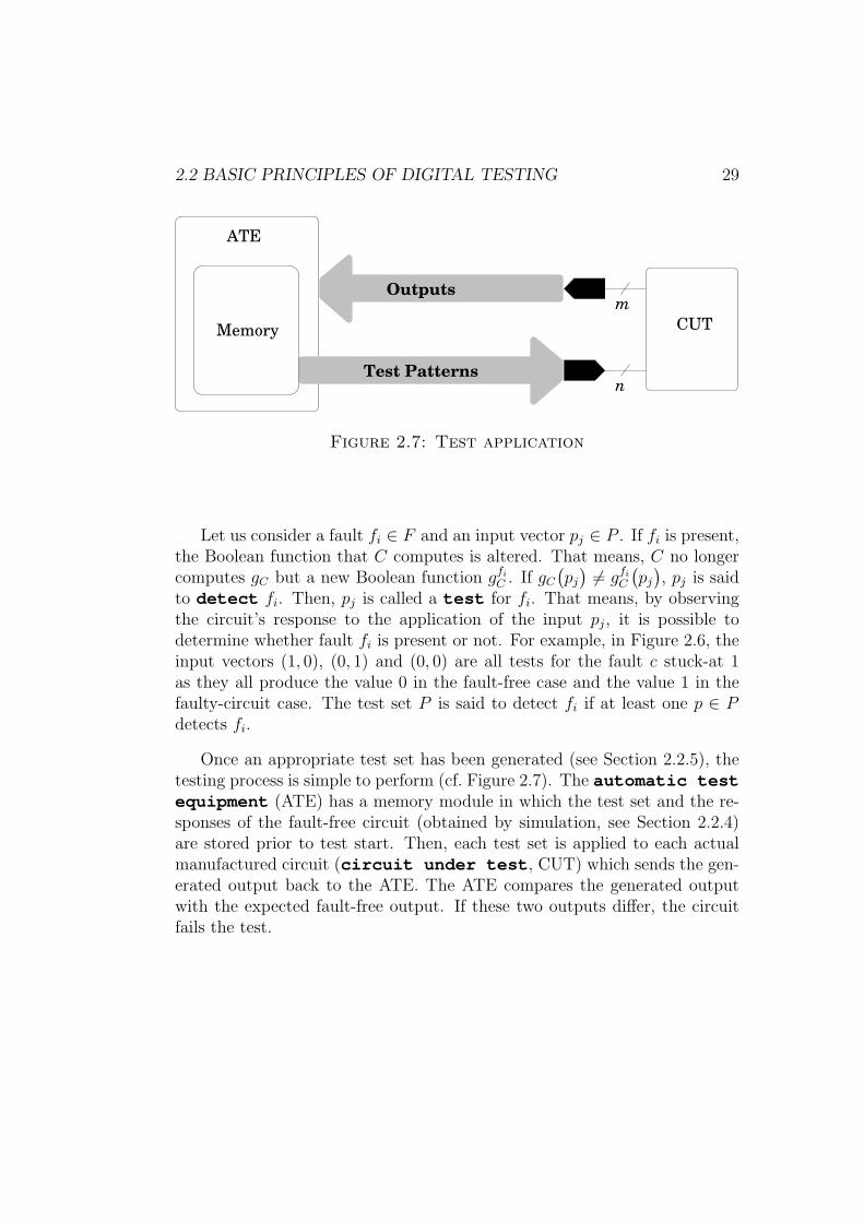
2.2 BASIC PRINCIPLES OF DIGITAL TESTING 29
n
CUT
ATE
m
Test Patterns
Outputs
Memory
Figure 2.7: Test application
Let us consider a fault fi ∈ F and an input vector pj ∈ P . If fi is present,the Boolean function that C computes is altered. That means, C no longercomputes gC but a new Boolean function gfi
C . If gC
(pj
)6= gfi
C
(pj
), pj is said
to detect fi. Then, pj is called a test for fi. That means, by observingthe circuit’s response to the application of the input pj, it is possible todetermine whether fault fi is present or not. For example, in Figure 2.6, theinput vectors (1, 0), (0, 1) and (0, 0) are all tests for the fault c stuck-at 1as they all produce the value 0 in the fault-free case and the value 1 in thefaulty-circuit case. The test set P is said to detect fi if at least one p ∈ Pdetects fi.
Once an appropriate test set has been generated (see Section 2.2.5), thetesting process is simple to perform (cf. Figure 2.7). The automatic testequipment (ATE) has a memory module in which the test set and the re-sponses of the fault-free circuit (obtained by simulation, see Section 2.2.4)are stored prior to test start. Then, each test set is applied to each actualmanufactured circuit (circuit under test , CUT) which sends the gen-erated output back to the ATE. The ATE compares the generated outputwith the expected fault-free output. If these two outputs differ, the circuitfails the test.

30 2. PRELIMINARIES
2.2.3 Fault coverage
The fault coverage is a measure to grade the quality of a test. In itsmost general form, it is defined as
fault coverage of a test set P =number of faults P detects
size of target fault list· 100%.
There are many other possibilities to compute fault coverage. Dependingon the used fault model, it may be necessary to consider several other factorswhen defining the detection metric, e.g. the probability for a fault to occuror the probability for a fault to be detected.
2.2.4 Simulation
2.2.4.1 Logic simulation
Logic simulation is the process of determining the steady-state logic valuesimplied at each circuit line by the application of an input vector to the circuit.
In its simplest form, the zero-delay logic simulation of a vectorp := (v1, v2, . . . , vn) ∈ Bn on a combinational logic block (combinational cir-cuit or core of a sequential circuit) assigns each component vi of the vector tothe corresponding primary input and computes the new logic value impliedat each line, where the lines are processed in topological order. These threesteps are repeated for each vector p ∈ P .
There are several techniques to accelerate logic simulation. One suchtechnique is the event-driven simulation. For example, when havingto simulate two test vectors p1 := (0, 0, 0, 0, 0) and p2 := (1, 0, 0, 0, 0), thefirst vector must be simulated as usual. But when simulating p2 it is notnecessary to recompute the logic value of every line in the circuit. It isenough to recompute the values of those lines which are in the output coneof the first primary input, as that is the only input whose logic value ismodified. Event-driven simulation is performed by assigning each primaryinput its new value as dictated by p2. If its new value differs from its oldvalue, its successor signals are inserted into a priority queue which ordersthe inserted signals topologically. Then, it is enough to recompute the logicvalues of those signals which are in the queue. Again, if the value of a signals taken from the queue changes, s’s successors have to be inserted into thequeue. These steps are repeated until the queue is empty.

2.2 BASIC PRINCIPLES OF DIGITAL TESTING 31
2.2.4.2 Fault simulation
Fault simulation is the process of determining the set of faults which aredetected by applying a test set to a circuit. Fault simulation is performed tocompute the fault coverage a test set achieves and as part of the test patterngeneration process.
The basic fault simulation algorithm is depicted in Figure 2.9. In thatpseudo-code, Cf stands for the faulty version of the circuit which is affectedby fault f . v(s) stands for the logic value a signal s has after performingthe fault-free simulation. vf (s) stands for the logic value a signal s hasafter performing the faulty-circuit simulation on Cf . Obviously, this simplealgorithm can also be applied when fault models other than the stuck-at faultmodel are used. Only the implementation of the fault-free simulation (line9) and of the faulty-circuit simulation (line 11) algorithms depends directlyon the used fault model.
Fault-free simulation of a test pattern p is the process of determining thesteady state of a fault-free circuit after applying p to its inputs. In the case ofthe stuck-at model, fault-free simulation is equivalent with logic simulation.For other fault-models, a fault-free simulation may be very complex. Fault-free simulation is performed to compute the fault-free responses that have tobe stored in the ATE memory.
Faulty-circuit simulation of a test pattern p is the process of determiningthe steady state of a circuit affected by a certain fault f after applyingp to its inputs. Usually, faulty-circuit simulation is performed like fault-free simulation. Only processing the fault site is slightly different. Its logicvalue is not computed as that of all other lines; it is derived from the faultdescription. Consider, for example, the circuit in Figure 2.8. The fault-freesimulation of (0, 1) is as follows. First, 0 is assigned to the primary input a
a
b
c
stuck−at−1c
0
1
0/1
fault−free faulty−circuitsimulation simulation
Figure 2.8: Example on fault simulation

32 2. PRELIMINARIES
and 1 is assigned to the primary input b. Then, the value of c is computed asvalue-of-a AND value-of-b = 1 AND 0 = 0. In the faulty-circuit simulation,instead of reading the values of a and b, the logic 1 is directly assigned tosignal c, as the fault c stuck-at-1 is present.
1 SIMPLE FAULT SIMULATION
2 Input : a circuit C3 a list of target faults F4 a test set P
5 Output : a list of detected faults F ′
6 BEGIN
7 let F ′ be an empty list of faults
8 for each test pattern p ∈ P ; do
9 perform fault-free simulation of pand record the fault-free outputv(s) for each signal s
10 for each fault f ∈ F ; do
11 perform faulty-circuit simulationof p on Cf
12 if v(z) 6= vf (z) for any primary output z ; then
13 move f from F to F ′
14 fi
15 done
16 done
17 return F ′
18 END
Figure 2.9: Algorithm: simple fault simulation
2.2 BASIC PRINCIPLES OF DIGITAL TESTING 33
2.2.5 (Automatic) test pattern generation
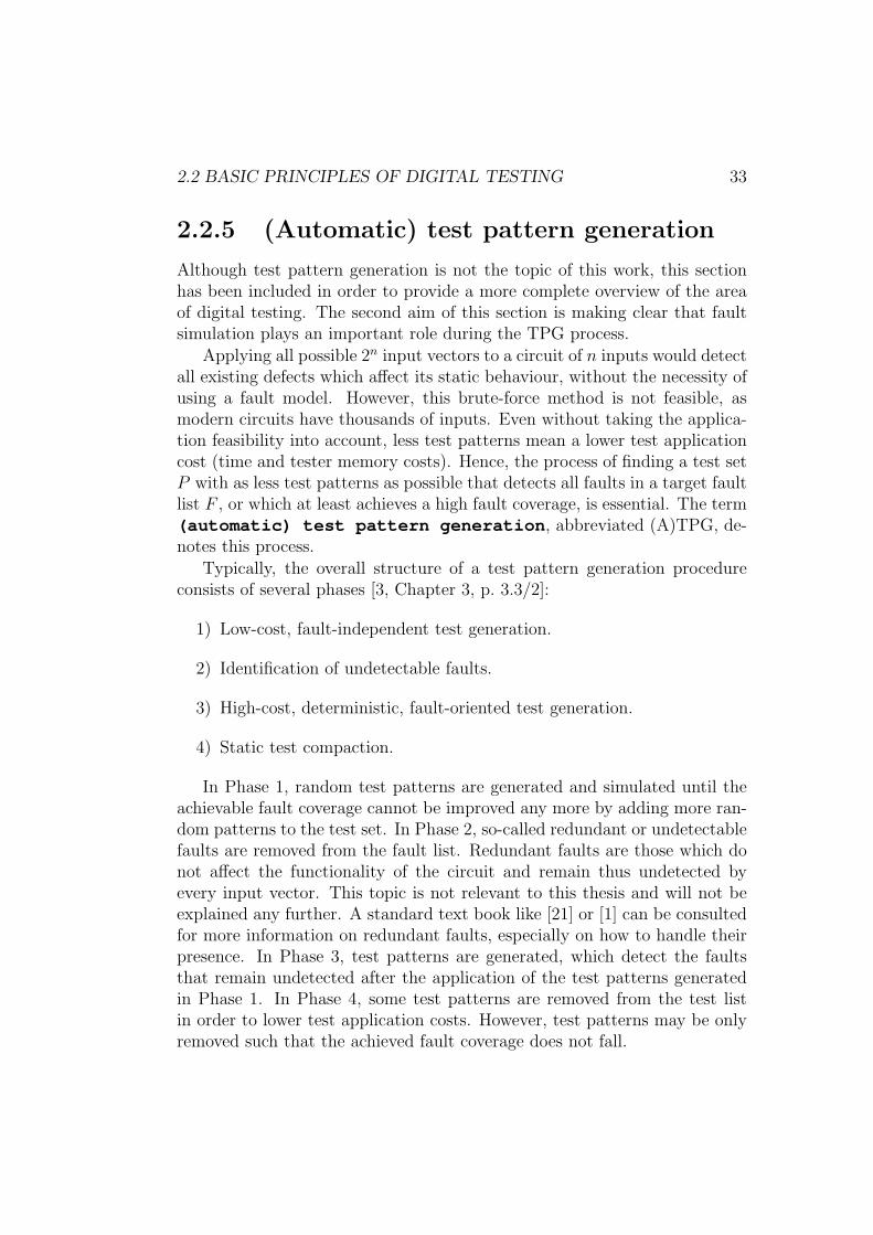
Although test pattern generation is not the topic of this work, this sectionhas been included in order to provide a more complete overview of the areaof digital testing. The second aim of this section is making clear that faultsimulation plays an important role during the TPG process.
Applying all possible 2n input vectors to a circuit of n inputs would detectall existing defects which affect its static behaviour, without the necessity ofusing a fault model. However, this brute-force method is not feasible, asmodern circuits have thousands of inputs. Even without taking the applica-tion feasibility into account, less test patterns mean a lower test applicationcost (time and tester memory costs). Hence, the process of finding a test setP with as less test patterns as possible that detects all faults in a target faultlist F , or which at least achieves a high fault coverage, is essential. The term(automatic) test pattern generation , abbreviated (A)TPG, de-notes this process.
Typically, the overall structure of a test pattern generation procedureconsists of several phases [3, Chapter 3, p. 3.3/2]:
1) Low-cost, fault-independent test generation.
2) Identification of undetectable faults.
3) High-cost, deterministic, fault-oriented test generation.
4) Static test compaction.
In Phase 1, random test patterns are generated and simulated until theachievable fault coverage cannot be improved any more by adding more ran-dom patterns to the test set. In Phase 2, so-called redundant or undetectablefaults are removed from the fault list. Redundant faults are those which donot affect the functionality of the circuit and remain thus undetected byevery input vector. This topic is not relevant to this thesis and will not beexplained any further. A standard text book like [21] or [1] can be consultedfor more information on redundant faults, especially on how to handle theirpresence. In Phase 3, test patterns are generated, which detect the faultsthat remain undetected after the application of the test patterns generatedin Phase 1. In Phase 4, some test patterns are removed from the test listin order to lower test application costs. However, test patterns may be onlyremoved such that the achieved fault coverage does not fall.

34 2. PRELIMINARIES
1 DETERMINISTIC TPGOVERALLPROCEDURE
2 Input : a circuit C3 a list of target faults F
4 Output : a test set P5 a list of undetectable faults F ′
6 BEGIN
7 let P be an empty test set
8 repeat
9 choose any fault f ∈ F
10 try to generate a test pattern p that detects f
11 if p can be generated ; then
12 add p to P
13 perform fault-free simulation of p on C
14 for each fault f ′ ∈ F ; do
15 perform faulty-circuit simulationof p on Cf ′
16 if p detects f ′ ; then
17 remove f ′ from F
18 fi
19 done
20 else
21 move f from F to F ′
22 fi
23 until F is empty
24 return P and F ′
25 END
Figure 2.10: Algorithm: deterministic TPG, overall procedure

2.3 DELAY FAULT MODELLING 35
Phase 3 is performed using the algorithm in Figure 2.10. One chooses atarget fault f and generates a test pattern p that detects it (line 10). Theexact algorithm for the deterministic test generation procedure of line 10depends on the used fault model. Since Phase 2 may fail to recognise someundetectable faults1, it is possible that there is no test for the chosen faultf . If the deterministic test generation procedure (line 10) cannot find a testfor f , f is marked as undetectable (line 21). If a test p is found, all faultswhich p detects are removed from the list, not only f (lines 14-19). This isdone such that the test set’s size remains low.
2.3 Delay fault modelling
In Section 2.2.1, some effects of manufacturing defects were listed. Thelast point in the list stated that some defects affected the timing of theinformation processing by the circuit. Defects that do not affect the logicalbehaviour of the circuit, but its timing, cannot be modelled using the stuck-atfault model. Instead, so-called delay fault models are used [21].
The most important delay fault models are the gate delay fault model[6], [35], the path delay fault model [44] and the segment delay faultmodel [18].
Gate delay faults: A circuit is said to have a (single) gate delay fault(GDF) in some gate, if the input or output of the gate is slow topropagate 0 → 1 (rising ) or 1 → 0 (falling ) transitions.
Path delay faults: A circuit is said to have a path delay fault (PDF), ifthe circuit has a path from a primary input si to a primary output so
which is slow to propagate rising or falling transitions from si to so.
Segment delay faults: A circuit is said to have a segment delay fault(SDF), if the circuit has a path of a given length L (or shorter) froma signal s1 to a signal s2 which is slow to propagate rising or fallingtransitions from s1 to s2.
While the GDF model is very simple and works with the unrealistic as-sumption that only one site is fully affected while others are not affected at
1The algorithms used in Phase 2 are meant to be fast and low-cost, but are usually notcomplete. The problem of identifying redundant faults is co-NP-complete.
36 2. PRELIMINARIES
all, the PDF model is the more general of both, as it models the cumulativeeffect of the delay variations of the gates and lines along the path. However,since the number of paths in the circuit can be very large, this model mayrequire much more time for test generation and application than the GDFmodel. The compromise between both extremes is the SDF model, whichworks with “short” paths. The parameter L can be chosen based on the avail-able statistics about the types of manufacturing defects. The SDF model ismore flexible than the GDF model but there are not as many faults as underthe PDF model. A comparative study on delay fault models is published in[28].
Relevant for this thesis is the line delay fault model [27], which canbe seen as a simplified version of the GDF model. A circuit is said to havea (single) line delay fault (LDF) if there is a line in the circuitwhich is slow to propagate rising or falling transitions, delaying them byan additional unknown, but fixed amount of time. That amount of time isalways denoted by δ in this thesis and is called the size of the fault .A fault is described by the fault site (the affected line) and by whetherrising or falling transitions are affected. Faults affecting rising transitionsare called slow-to-rise LDFs, those affecting falling transitions are calledslow-to-fall LDFs. A slow-to-rise fault affecting the line or signal withidentification number i is denoted in this thesis by iR. A slow-to-fall faultaffecting signal i is denoted by iF.
2.3.1 Test application
Testing for delay faults requires the application of two successive test pat-terns (a test pair ) to the CUT. The first pattern (initialisationvector ) brings the CUT into a known and stable state. The second testpattern (propagation vector ) excites the fault and propagates the faulteffect to an output by inducing a rising or falling transition at one or moreinputs of the CUT. If the circuit is correct, its state changes meeting the sametiming constraints as the fault-free circuit. This testing method is known astwo-pattern testing . Detailed information on two-pattern testing canbe found in [4] and literature cited there.
For a slow-to-rise LDF f , exciting f means inducing at the fault site arising transition that can be delayed if f is present. A slow-to-fall LDF isexcited if a falling transition is induced at the fault site.

2.3 DELAY FAULT MODELLING 37
74
65
1
1
03
2
1
0
registering
time
4R
Figure 2.11: Detection of an LDF
Given a test pattern pair p, the initialisation vector is denoted by p1 andthe propagation vector by p2.
A test pair p that detects an LDF iR (iF) must have the followingproperties:
• p1 must induce the logic value 0 (1) at signal i.
• p2 must induce the logic value 1 (0) at signal i thus launching a rising(falling) transition at the fault site.
• Both p1 and p2 must sensitise a path from the fault site to a primaryoutput of the circuit, thus allowing the fault effect to become visible atan output.
A path is said to be sensitised if all its lines are sensible to the fault,i.e. if the behaviour of all its signals is different in the fault-free and thefaulty-circuit case. Consider, for example, the circuit in Figure 2.11. Thetest pair 0110/1110 makes the path composed of bold lines sensible to fault4R. When 0110/1110 is applied, signal 2 remains stable at logic 1 duringthe application of both vectors. As 1 is the non-controlling value of gate5, the behaviour of gate 5’s output depends exclusively on the behaviour ofthe fault site, signal 4. Analogously, signal 3 remains stable at logic 0, thenon-controlling value of gate 6. Thus, the behaviour of the circuit’s primaryoutput depends exclusively on the behaviour of signal 5. Altogether, if thefault 4R is present, the induced rising transition at signal 4 is delayed. Thisdelays signal 5’s falling transition, which delays signal 6’s falling transition.If the delay is large enough, the expected logic 0 will arrive at the outputafter the registering time, at which the wrong value 1 is read, thus provingthe circuit to be faulty.

38 2. PRELIMINARIES
The “classical method” to apply a test pair p is the following: First, p1
is applied to the CUT. All internal signals are allowed to stabilise (which isachieved in practice by holding the inputs constant for several cycles). Then,p2 is applied to the inputs. In the next clock cycle the outputs are evaluated.If the value at any output does not correspond to the expected value, thenthe propagation must have been too slow and the CUT is proven faulty.
Delay fault tests must obviously be applied at a device’s nominal speed(at-speed testing ). In contrast to the classical test method, it is pos-sible to apply all test pairs just one after another, without waiting for thecircuit’s signals to stabilise. An interesting empirical result is reported in [31].By performing experiments with a sample of manufactured ICs, the authorsfound that omitting the waiting actually reduces the number of defectivechips passing the test.
2.3.2 Application of two-pattern testing to
sequential circuits
Most testing concepts remain largely unchanged when considering sequentialinstead of combinational circuits. Alas, that is not the case of two-patterntesting. When working with sequential circuits, two-pattern testing becomesconsiderably more difficult than when applying it to combinational circuits.
In the most general case, the secondary inputs and secondary outputsof a sequential circuit are not accessible from outside of the circuit. Thiscircumstance may forbid the application of necessary values (values which arerequired to sensitise the path or to induce the proper transition at the faultsite) to the secondary inputs; and, if the fault effect can only be propagatedto a secondary output, the fault effect becomes unobservable.
It may be possible to write a necessary value into a memory element byapplying the synchronising sequences technique (page 22). However, thistechnique does not always work. If the combinational core’s structure is toocomplex, such a sequence may not exist at all. For circuits with a largenumber of secondary inputs, this writing approach becomes useless.
A better approach is to use a standard method for reducing testingproblems for sequential circuits to ones for combinational circuits, namelyscan design . See, for example, [34, Section 2.1.4] for a concise introduc-tion; or [1], [21] for detailed information on this topic.
Figure 2.12 illustrates the main idea of scan design. The combinationalcore of a sequential circuit with 3 flip-flops is shown. There are two addi-

2.3 DELAY FAULT MODELLING 39
D−FF
D−FF
D−FF
n
InputsSecondary
scan_enable
PrimaryInputs
scan_out
OutputsSecondary
PrimaryOutputs m
scan_in
CORE
COMBINATIONAL
Figure 2.12: Scan design

40 2. PRELIMINARIES
tional inputs, scan in and scan enable; and one additional output, scan out.scan enable controls additional multiplexers between the flip-flops. Whenscan enable is inactive, the multiplexers are switched to let through thevalues from the core’s secondary outputs, and the circuit is in its normaloperation mode. When scan enable is activated, the flip-flops are connectedto form a chain called the scan chain . By applying values to the scan ininput, arbitrary values can be shifted into the flip-flops, while their contentcan be shifted out over the scan out output.
When all flip-flops are part of the scan chain (full scan ), applyingarbitrary initialisation vectors is possible. However, scan does not solve thesecond problem that arises when applying two-pattern testing to sequentialcircuits. Since the two vectors of a test pair have to be applied in consecutiveclock cycles, it is not possible to apply arbitrary propagation vectors, as theshifting of all values for the secondary inputs requires as much clock cyclesas there are flip-flops.
Applying the test pair according to the “classical” test application methodintroduced in Section 2.3.1, which allows the effects of the application of theinitialisation vector to stabilise over several clock cycles, does also not solvethis problem. All the input values specified by the propagation vector mustbe applied simultaneously to all primary and secondary inputs of the CUT.
Hence, two-pattern testing can only be applied to a full-scan-circuit if thepropagation vector is such that the values that it specifies for thesecondary inputs are obtained through the functional path as response tothe application of the initialisation vector.
Furthermore, each test pair can only be applied independently of allothers in the test set, due to the additional clock cycles needed to scanin the initialisation vector and the additional clock cycles needed to scan outthe secondary output values after the application of the propagation vector.
There are enhanced scan techniques that allow storing arbitrary valuesinto several flip-flops simultaneously. However, this benefit is accompaniedof a high hardware overhead.

2.4 FAULT COVERAGE UNDER RESISTIVE FAULT MODELS 41
2.4 Fault coverage under resistivefault models
In almost any semiconductor manufacturing technology, conducting wiresconnected in an unintended way are a prominent class of defects. Bridgingfault models have been created to model this type of defects. In its moregeneral form, this model assumes that two lines are bridged, e.g. due to aconducting contamination touching both lines, thus creating an unintendedconnection between them. If both lines conduct the same logic value (i.e. thesame voltage level) there is no malfunction. However, if opposite logic valuesare present at the bridged lines, faulty behaviour may arise. Then, one orboth bridged lines are affected. Depending on the assumptions made, thefaulty behaviour can be described using a variety of different bridging faultmodels. Among these are the resistive bridging fault models,under which the bridge has a resistance. More detailed information on thistopic can be found in [11], [12], [13] and [34, Section 2.3.4]. In this section,some definitions taken from that literature are introduced. These definitionswill be needed in Chapter 6.
Working with resistive fault models requires taking into account the re-sistance, which is an unknown and unpredictable parameter [41]. A bridgingfault may be detected by a test vector for one resistance, while the bridgebetween the same affected nodes may not be detected by the same vector ifthe bridge has a different resistance. For example, the resistance may be sohigh, that the fault cannot be excited. If the bridge conductance is too low,the bridged signals cannot affect each other.
This ambiguity changes the concept of fault coverage in fundamentalmanner. It is not longer possible to speak of a detected or an undetectedfault. It is necessary to find a way of measuring the probability for thefault’s detection, depending on the probability that the bridge has a certainresistance.
Renovell et al. [40], [38], [39] introduced the concept of an AnalogueDetectability Interval (ADI). The simulation yields for each faultand each output a resistance range [r1; r2], the ADI, such that the shortmodelled by the fault is detected by the test set if and only if its resis-tance r meets the condition r1 ≤ r ≤ r2. Typically, r1 is 0 Ω, but thisdoes not need to be the case. For circuits having reconvergencies and se-quential circuits, the ADI may be the union of multiple disjoint intervals[r1,1; r1,2] ∪ [r2,1; r2,2] ∪ · · · ∪ [rN,1; rN,2] [40].

42 2. PRELIMINARIES
Let the CUT have m outputs, and let f be a fault. For i = 1, 2, . . . ,m anda test pattern p, ADIi(p) denotes the ADI propagated to the i-th outputby simulating p. Given a test set P , the C-ADI of f is defined as
C-ADI (f) :=⋃p∈P
m⋃i=1
ADIi(p).
The C in C-ADI stands for “covered by the test set”. The C-ADI of a faultis the union of all ranges of resistances for which the fault is detected by P .
There are several fault coverage definitions basing on C-ADI. In the orig-inal literature they are just called fault coverage. Here, the same notationand terminology as in [34, Section 2.3.4] is used.
Let ρ(r) be the probability density function of the short resistance r. In[39] the Normal distribution is suggested to describe ρ(r). Thepessimistic fault coverage (P-FC) introduced in [39] is defined forone fault f as
P-FC (f) :=
∫C-ADI(f)
ρ(r)dr
+∞∫0
ρ(r)dr
· 100%.
This definition relates the “fraction” of the ranges in which the fault is de-tected to the complete range from 0 to +∞, weighted by ρ. For a fault listF , the average fault coverage is defined as
P-FC (F ) :=
∑f∈F
P-FC (f)
|F |
In [40], a second definition is proposed. G-ADI is defined as C-ADI of anexhaustive test set. G stands for “global”. The corresponding fault-coveragedefinition is
G-FC (f) :=
∫C-ADI(f)
ρ(r)dr∫G-ADI(f)
ρ(r)dr· 100%.
This definition can be considered to be exact, but an exhaustive test setconsists of 2n vectors for circuits with n inputs. Thus, G-ADI can only bemeasured for circuits with relatively few inputs.

2.4 FAULT COVERAGE UNDER RESISTIVE FAULT MODELS 43
The third fault coverage definition was introduced by Walker in [23].E-FC (E means “excitation”) is defined as
E-FC (f) :=
∫C-ADI(f)
ρ(r)dr
Rmax∫0
ρ(r)dr
· 100%,
where Rmax is the maximum size the resistance may have as to excite thefault.
A fourth fault coverage definition was introduced in [12]. O-FC (O standsfor “optimistic”) is defined as
O-FC (f) :=
0% if C-ADI (f) = ∅100% else
.
Under O-FC, it is enough that a fault is detected for any resistance in orderto regard the fault as detected.
The following relationship is shown in [12]:
P-FC (f) ≤ E-FC (f) ≤ G-FC (f) ≤ O-FC (f) .
For a fault list F , the average fault coverages G-FC (F ), E-FC (F ) andO-FC (F ) are defined analogously to P-FC (F ).

44 2. PRELIMINARIES

3
Simulating Dynamic Effectsof Resistive Opens
The aim of the work presented in this thesis is designing and implementing asimulator for resistive opens. These opens are also called weak and havea resistance of less than 10 MΩ [43]. Resistive opens are defects whichmanifest themselves as lines with an elevated resistance or as resistive viasand contacts. They still let the circuit work, but increase the delay of pathsgoing through the fault site [25], [29]. In this work, resistive opens aremodelled using the single line delay fault model. In [36] they are modelledas gate delay faults. Modelling them as line delay faults instead, does notconstitute a large modification. This just allows the fault to occur at thecircuit’s inputs, which are not fed by gates.
When modelling a resistive open with a resistance r by an LDF, thefault’s size δ depends on r. r is an unpredictable random parameter [41].A simulator is to be designed and implemented that accepts the followingarguments:
• a combinational or sequential circuit C (gate-level net-list and risingand falling delay times of each gate type) with n primary inputs andm primary outputs;
• a list F of LDFs, from now on called the fault list ;
• and a set P of test pairs, from now on called the test set ;
The simulator shall accomplish the following tasks:
• perform fault simulation and compute C-ADI (f) for each fault f in F ;
45

46 3. SIMULATING DYNAMIC EFFECTS OF RESISTIVE OPENS
• compute the fault coverage achieved by the application of P to C.
Let f ∈ F be an LDF modelling an open with resistance r. Analogouslyto the definition in Section 2.4, C-ADI (f) is a set of possibly disjoint rangesof resistances. It has the form
C-ADI (f) :=[r1,1; r1,2], [r2,1; r2,2], . . . , [rN,1; rN,2]
,
where ri,1 ∈ N and ri,2 ∈ ri,1, ri,1 + 1, . . . ∪ +∞ for all i = 1, 2, . . . , N ;and the property that P detects f if and only if r ∈ [ri,1; ri,2] for somei = 1, 2, . . . , N . The ranges in C-ADI (f) are called detectionresistance ranges of f .
n
2+ 5+ TC=8δ δ f
Figure 3.1: Detection interval of an LDF
What is the purpose of computing C-ADI (f) of a fault f? Let us considerthe application of a test pair p on the example circuit shown in Figure 3.1.In the fault-free case, the circuit’s output signal is stable at logic 0 until time2. The application of p2 induces a 1-pulse between time 2 and time 5. Aftertime 5, the output remains stable at logic 0. The clock sampling time TC is8. Let a fault f of size δ cause the 1-pulse at the circuit’s output to beginat time 2 + δ and to end at time 5 + δ. p detects f only if the presence of fcauses the circuit’s output to have the logic value 1 (the wrong output value)at time TC, which is the time the circuit’s output values are registered at.1
That means, p detects f if and only if 2 + δ ≤ TC < 5 + δ, i.e. if 3 < δ ≤ 6.δ will meet this constraint only if the modelled open’s resistance r is in a
1Usually, a combinational circuit does not stand alone. Several combinational blocksare part of a system and synchronised using a universal clock. For the purpose of commu-nication among the combinational blocks, their outputs may be stored into register bankswhich are writable at times TC, 2 · TC, 3 · TC, etc.

3.1 OVERALL STRUCTURE OF THE RO-SIMULATOR 47
certain range [r1; r2]. As was already said, r is an unpredictable parameter,so it is not guarantee-able that r is in [r1; r2] for every actual manufacturedcircuit that has the open. The open will remain undetected by p if not. Inorder to improve fault coverage, it may be necessary to find additional testpairs which detect the open if its resistance is in ranges other than [r1; r2].
Thus, simulating the test set and computing the C-ADI of faults is es-sential during TPG as an indicator of whether more test pairs have to begenerated to achieve an acceptable fault coverage.
Throughout this thesis, our simulator is called RO-simulator (standsfor “resistive-opens-simulator”).
3.1 Overall structure of theRO-simulator
The RO-simulator works in three phases:
1) Delay fault simulation is performed and for each fault f in F a so-calleddetection set of delay size intervals , abbreviatedDSdel (f), is computed. It has the form
DSdel (f) :=[a1,1; a1,2], [a2,1; a2,2], . . . , [aM,1; aM,2]
,
where ai,1 ∈ N and ai,2 ∈ ai,1, ai,1 + 1, . . . ∪ +∞ for alli = 1, 2, . . . ,M ; and the property that P detects f if and only if f ’ssize δ is in [ai,1; ai,2] for some i = 1, 2, . . . ,M . The intervals in DSdel (f)are called detection delay size intervals of f .
2) For each fault f in F , C-ADI (f) is computed based on DSdel (f).
3) The overall fault coverage that P achieves is computed based onC-ADI (f) of all faults f ∈ F .
Figure 3.2 shows how the simulator works. In that pseudo-code, Cf
stands for the faulty version of the circuit which is affected by fault f .Lines 10 through 18 correspond to Phase 1 of the RO-simulator. Phase 1’s
structure is exactly that of a “classical” fault simulation algorithm (cf. Figure2.9 on page 32). Here, instead of just marking the faults as detected, theirdetection delay size intervals are computed (line 15) since, according to the

48 3. SIMULATING DYNAMIC EFFECTS OF RESISTIVE OPENS
1 SIMULATION OF DYNAMICEFFECTSOF RESISTIVE OPENS
2 Input: a combinational circuit C3 a fault list F4 a test set P
5 Output: an array RES holding C-ADI (f) for each f ∈ F6 the achieved fault coverage FC
7 BEGIN
8 let RES be the array that willhold C-ADI (f) for each f ∈ F .
9 let DEL be the array that willhold DS del (f) for each f ∈ F .
10 for each test pair p ∈ P ; do
11 perform fault-free simulation of p
12 for each fault f ∈ F ; do
13 if f is excited by p ; then
14 perform faulty-circuit simulationof p on Cf
15 determine detection delay size intervalsof f under p and add them to f ’sdetection set of delay sizeintervals DEL[f ]
16 fi
17 done
18 done
19 for each fault f ∈ F ; do
20 convert DEL[f ] into RES[f ]
21 done
22 compute FC out of RES
23 return RES and FC
24 END
Figure 3.2: Algorithm: overall proceeding of the RO-simulator

3.1 OVERALL STRUCTURE OF THE RO-SIMULATOR 49
fault model, a fault is detected only with a certain probability depending onits size.
An example on how the fault-free simulation (line 11) works is in Section5.1.1, a detailed description in Section 5.2.1. An example on how the faulty-circuit simulation (line 14) works for a test pattern p and a fault f , is inSection 5.1.2, a detailed description in Section 5.2.2. An example on how thecomputation of a set of detection intervals (line 15) works for a test pattern pand a fault f , is in Section 5.1.3, a detailed description in Section 5.2.3. Theobtained detection intervals tell what size f must have such that p detectsit. The final set of detection intervals for f is the union of the sets obtainedfor each test pair.
A short remark must be made on line 13 in Figure 3.2, although this hasbeen mentioned in the preceding chapter. A fault iF is excited by a testpair p := (p1, p2) if the application of p1 causes signal i to stabilise at logic 1while the application of p2 causes signal i to stabilise at logic 0. A fault iRis excited if the application of p1 causes signal i to stabilise at logic 0 whilethe application of p2 causes signal i to stabilise at logic 1.
Finally, it is necessary to say that the RO-simulator’s Phase 1 is basedon the delay fault simulation method (PR-simulator ) in [36]. However,techniques and algorithms of the PR-simulator were modified or extended.These modifications will be explained later. If those modifications have beenintroduced by other authors in the past, we are not aware of that. Chapters 4and 5 deal in detail with the implementation of Phase 1 of the RO-simulator.
In Phase 2 (lines 19 through 21 in Figure 3.2), C-ADI (f) is computed outof DSdel (f). This is done for each fault f independently of all other faults.
Given a fault f and its detection set of delay size intervals,DSdel (f) :=
[a1,1; a1,2], [a2,1; a2,2], . . . , [aM,1; aM,2]
, it is enough to find a
map κ from the set of delay fault sizes to the set of resistances, such thatκ(δ) = r if an open with resistance r causes a delay of δ. Then,C-ADI (f) =
[κ(a1,1); κ(a1,2)], [κ(a2,1); κ(a2,2)], . . . , [κ(aM,1); κ(aM,2)]
.
Deriving the exact, physically accurate map is out of the scope of thiswork. Proposals for the mapping κ exist [24], but in this first implementationof the RO-simulator, a linear mapping is used. In future it will be replaced bymore accurate models as soon as these become available. The RO-simulatorwas implemented such that new mapping models can be easily integratedinto it.

50 3. SIMULATING DYNAMIC EFFECTS OF RESISTIVE OPENS
In Phase 3 (line 22 in Figure 3.2), the achieved fault coverage is computeddepending on the detection sets of resistance ranges. This topic is discussedin Chapter 6. Due to the linear mapping mentioned above, the fault coveragefigures presented in Chapter 7 directly depend on the detection sets of delayfault intervals.
3.2 Application of RO-simulation tosequential circuits
Obviously, only Phase 1’s implementation depends on whether the givencircuit is combinational or sequential. The delay-to-resistance mapping per-formed in Phase 2 is done by local analysis and does not depend on theCUT being combinational or sequential. The fault coverage computationperformed in Phase 3 is also independent of this question.
Phase 1 implements delay fault simulation which requires two-patterntesting (cf. Section 2.3). As was explained in Section 2.3.2, two-patterntesting cannot be applied to all sequential circuits, but it can be applied tofull-scan-capable circuits. However, there is the restriction that each testpair must be applied independently of all others in the test set, and that thepropagation vector of each test pair is such that, the values it specifies forthe secondary inputs are obtained through the functional path as responseto the application of the initialisation vector.
The RO-simulator can work with both combinational and sequential cir-cuits. The delay fault algorithms which form Phase 1 were all enhanced asto accept and process secondary inputs and secondary outputs.
However, the RO-simulator can only be used on full-scan-capable sequen-tial circuits, as the secondary inputs are treated as fully accessible duringthe application of each initialisation vector and the secondary outputs aretreated as fully observable during the application of each propagation vector.Enhanced-scan-capability is not a prerequisite.

4
More Preliminaries
In Chapter 5 Phase 1’s design and implementation is discussed. In order tokeep the chapters of this thesis rather short and thus, more easy to read, thischapter has been included. This chapter introduces some definitions whichare necessary to understand the following chapter; as well as the basics onwaveforms and so-called signal descriptors. These are the data structuresused to specify the simulation algorithms of the next chapter.
4.1 Definitions and conventions
When building a simulator for delay faults, it is necessary to establish a set ofrules that dictate how to represent and handle time and other concepts thatdepend on time. This set of rules is presented in this section. None of theconcepts presented here constitutes original work. These concepts are usedin several works that deal with the timing behaviour of circuits. However,other authors may use a different terminology.
4.1.1 Time issues and test application
In this work, points in time, time interval lengths and LDF sizes are repre-sented by integers greater or equal 0. Additionally, there is a point in timedenoted by −∞. This point in time plays a special role which will be ex-plained below. The base time unit of the RO-simulator are picoseconds. Forsimplicity, time units are mainly left out in this thesis.
51

52 4. MORE PRELIMINARIES
For simplicity in the case of combinational circuits, and in order to beable to handle sequential circuits, the consecutive application of several testpairs is not considered in this work. Each test pair is assumed to be appliedindependently of all others in the test set.
A signal s is said to be stable after the application of a test vectorwhen s’s logic value does not change any more.
When simulating a test pair p, the classical method presented on page 37is used. After the application of p1, all signals are allowed to stabilise beforeapplying p2. The point in time, at which all signals in the circuit becomestable after having applied p1, is denoted by −∞. p2 is applied at time 0.
It would also be possible to apply p1 at any time t and p2 at time t+TC.But there is no difference in proceeding the first or the second way. Sincethis work deals with delay faults which can only be excited by inducing atransition at the fault site, only the effects set in motion by applying p2 areof interest.
In this context, four parameters are defined for each signal s in the circuit.These parameters are also defined in [20] and [36].
IV (s): Initial value of s. This is the stable logic value of s after theapplication of p1 (in other words, s’s logic value at time −∞).
FV (s): Final value of s. This is the stable logic value of s after theapplication of p2 in the fault-free simulation.
EAT (s): Earliest arrival time of s. This is the first point in timeat which the value of s changes from IV (s) to a different value as areaction to the application of p2 in the fault-free simulation.
LST (s): Latest stabilisation time of s. This is the last point intime at which the value of s changes to FV (s) as a reaction to theapplication of p2 in the fault-free simulation.
Consider the example in Figure 3.1 (page 46). Let s be the depictedcircuit’s only primary output signal. Then, IV (s) and FV (s) are both0, EAT (s) equals 2 (in the fault-free simulation, δ equals 0) and LST (s)equals 5.
Note that EAT (s) and LST (s) have a very important meaning. For anysignal s, its logic value is guaranteed to be stable between time −∞ andtime EAT (s) and for ever after time LST (s). Thus, if a signal s’s logicvalue never changes in reaction to the application of p2 in the fault-freesimulation, EAT (s) have to be defined as +∞ and LST (s) as −∞.

4.1 DEFINITIONS AND CONVENTIONS 53
0
1
2
876
4
3/3
5
2/1
3
2/2
1/33/5
0
0
0
2=0+2
3=0+3
4=2+2
8=3+511=8+3
Figure 4.1: Computing PLST: an example
A path is said to be stable after the application of an input vectorwhen all signals in the path are stable. The guaranteed time after which apath has stabilised is called latest stabilisation time (LST) of thepath.
PLST (stands for “latest stabilisation time of any path”) is defined as theguaranteed time after which all paths in the fault-free circuit have stabilisedafter applying any input vector. I.e. PLST is the largest path LST amongall paths in the circuit. Consider, for example, the circuit in Figure 4.1.Suppose that all signals are stable. Then, let an unknown input vector beapplied at time 0. Signals 0, 1 and 2 become stable at time 0 as they areprimary inputs. Signal 3 becomes stable at time 2 as all its predecessorsbecome stable at time 0 and gate 3 needs 2 time units to produce both risingand falling transitions. Analogously, signal 4 becomes stable at time 3. Inthe worst case, signal 5 becomes stable at time 4 = 2 + 2, as the latest pointin time at which both its predecessor signals are guaranteed to be stable istime 2; and because 2 time units is the largest time gate 5 needs to producea transition. Analogously, the worst case stabilisation time of signal 6 is8 = 3 + 5, and the worst case stabilisation time of signal 7 is 11 = 8 + 3.Thus, PLST equals 11. Figure 4.2 depicts the algorithm used to computePLST. The primary inputs are assigned the latest stabilisation time 0 (line8). For each other signal, its latest stabilisation time is computed as the sumof the latest time at which all its predecessors are stable and the largest timeits source gate needs to produce a transition (line 10). Finally, PLST is thelargest latest stabilisation time among all outputs of the circuit (line 13).
The clock period length TC is usually chosen as PLST·(100+SF)%, whereSF is a safety margin . In this work, SF is set to 20, i.e. TC := 1.2·PLST.In the example of Figure 4.1, TC is set to 13.

54 4. MORE PRELIMINARIES
1 PLST computation
2 Input: a circuit C containing NS-many signals
3 Output: an amount of time representing PLST
4 BEGIN
5 initialise an array LST of length NS
6 for i = 1 to NS ; do
7 if signal i is a primary or secondary input ; then
8 set LST [i] := 0
9 else
10 set LST [i] := max
LST [j]
∣∣∣∣∣signal j is apredecessor signalof signal i
+ maxRD(i) , FD(i)
11 fi
12 done
13 return max
LST [j]
∣∣∣∣∣signal j is aprimary or secondaryoutput
14 END
Figure 4.2: Algorithm: computation of PLST
73 11
1c
Figure 4.3: Example on input intervals of a single-input gate
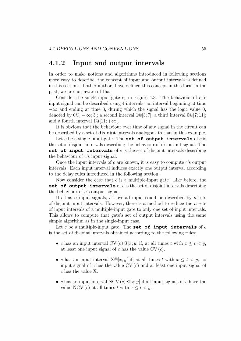
4.1 DEFINITIONS AND CONVENTIONS 55
4.1.2 Input and output intervals
In order to make notions and algorithms introduced in following sectionsmore easy to describe, the concept of input and output intervals is definedin this section. If other authors have defined this concept in this form in thepast, we are not aware of that.
Consider the single-input gate c1 in Figure 4.3. The behaviour of c1’sinput signal can be described using 4 intervals: an interval beginning at time−∞ and ending at time 3, during which the signal has the logic value 0,denoted by 0@]−∞; 3[; a second interval 1@[3; 7[; a third interval 0@[7; 11[;and a fourth interval 1@[11; +∞[.
It is obvious that the behaviour over time of any signal in the circuit canbe described by a set of disjoint intervals analogous to that in this example.
Let c be a single-input gate. The set of output intervals of c isthe set of disjoint intervals describing the behaviour of c’s output signal. Theset of input intervals of c is the set of disjoint intervals describingthe behaviour of c’s input signal.
Once the input intervals of c are known, it is easy to compute c’s outputintervals. Each input interval induces exactly one output interval accordingto the delay rules introduced in the following section.
Now consider the case that c is a multiple-input gate. Like before, theset of output intervals of c is the set of disjoint intervals describingthe behaviour of c’s output signal.
If c has n input signals, c’s overall input could be described by n setsof disjoint input intervals. However, there is a method to reduce the n setsof input intervals of a multiple-input gate to only one set of input intervals.This allows to compute that gate’s set of output intervals using the samesimple algorithm as in the single-input case.
Let c be a multiple-input gate. The set of input intervals of cis the set of disjoint intervals obtained according to the following rules:
• c has an input interval CV (c) @[x; y[ if, at all times t with x ≤ t < y,at least one input signal of c has the value CV (c).
• c has an input interval X@[x; y[ if, at all times t with x ≤ t < y, noinput signal of c has the value CV (c) and at least one input signal ofc has the value X.
• c has an input interval NCV (c) @[x; y[ if all input signals of c have thevalue NCV (c) at all times t with x ≤ t < y.

56 4. MORE PRELIMINARIES
1
s3
2c
7input waveform of
13
10 13
5
7 11
2cs2
s
5
Figure 4.4: Example on input intervals of a multiple-input gate
Consider, for example, the multiple-input gate c2 in Figure 4.4. Signal s2
has the unknown value X until time 5. At the same time, signals s1 and s3
have the value 1. As 1 is NCV (c2), c2’s input between time −∞ and time 5depends only on signal s2. Thus, the first input interval of c2 is X@]−∞; 5[.Between time 5 and time 7 all three signals have the value 1. Thus, thesecond input interval of c2 is 1@[5; 7[. Between time 7 and time 11 signal s1
has the logic value 0, CV (c2). Between time 10 and time 13 signal s3 hasthe logic value 0. Altogether, between time 7 and time 13 there is always aninput signal of c2 which has the logic value 0. Thus, the third input intervalof c2 is 0@[7; 13[. After time 13 all three input signals are stable at logic 1.Thus, the fourth input interval of c2 is 1@[13; +∞[.
Altogether, the set of input intervals of c2 comprises the intervalsX@] − ∞; 5[, 1@[5; 7[, 0@[7; 13[ and 1@[13; +∞[. These intervals arerepresented by the waveform in the lowest part of Figure 4.4. These fourintervals are enough to determine c2’s output intervals. Each interval in-duces exactly one output interval according to the delay rules that follow inthe next section.
4.1 DEFINITIONS AND CONVENTIONS 57
4.1.3 Delay model
The term delay model shall not be confounded with the term delay faultmodel. A delay model is a set of rules specifying how and when a gateresponds to the change of one or more of its inputs.
[20] introduces the distributed delay model , which tries to reflectthe fact that delays in actual fabricated circuits vary between upper and lowerbounds, especially due to manufacturing process variations. The model hasthe following characteristics:
1) The delay through a gate may vary depending on whether the gateproduces a rising or a falling transition.
2) Different gates of the same type may have different delays.
3) A gate has some inertia in responding to changes in its input values.That means that certain input pulses are filtered out in the gateresponse if they are too short.
Here, a simplified version of the distributed delay model is used:
1) The delay through a gate c is defined by its rising delay time RD (c)and by its falling delay time FD (c).Let s be c’s output signal. Given the set of input intervals of c, the setof output intervals is computed in the following way:
(i) Each input interval with value 1 or value 0 induces one outputinterval according to the rules listed in Table 4.1.
(ii) s is defined to have the unknown value X at all times t which arenot in any interval computed in the first step.
The table is read in the following way: consider, for example, the ta-ble’s first row. An input interval 0@[x; y[ induces the output interval0@[x+FD (c) ; y+RD (c) [ if the gate c is not inverting (if c is inverting,the table’s second row determines the output interval). However, theoutput interval is only induced if the additional condition x+FD (c) ≤ yis met. If this additional condition is not met, no output interval is in-duced at all. The intuition behind this additional condition is bestexplained by means of an example. Let I be a 1-interval and let cbe non-inverting. I begins with a rising transition τ1 and ends with afalling transition τ2. τ1 induces a rising transition τ3 at c’s output; but

58 4. MORE PRELIMINARIES
input int. c inv. add. condition output interval
0@[x; y[ no x + FD (c) ≤ y 0@[x + FD (c) ; y + RD (c) [
0@[x; y[ yes x + RD (c) ≤ y 1@[x + RD (c) ; y + FD (c) [
1@[x; y[ no x + RD (c) ≤ y 1@[x + RD (c) ; y + FD (c) [
1@[x; y[ yes x + FD (c) ≤ y 0@[x + FD (c) ; y + RD (c) [
Table 4.1: Delay model
if τ2 arrives before τ3 has been produced, it is not possible to guaranteethat c is still able to produce τ3.In the table, x is allowed to be −∞ and y is allowed to be +∞. Addi-tionally, we define ±∞+ k = ±∞ where k is RD (c) or FD (c).
2) The second property of the distributed delay model can be modelledas an increase or decrease from the nominal delay by a maximum of σ[20, p. 79]. For simplicity, this extension is not used in this work. Here,RD (c) and FD (c) are single fixed integers.
3) The gate’s inertia (Property 3 of the distributed delay model) is ac-counted for to some extent by this simplified model’s first property.Let us illustrate this with an example (see Figure 4.5). Let c be anAND gate, let RD (c) be 7, FD (c) be 3. The input interval 1@[t; t + a[induces the output interval 1@[t+7; t+a+3[, but only if t+7 ≤ t+a.That means that the output interval is induced only if a ≥ 7. I.e. 1-pulses shorter than 7 time units are filtered out.
s1
s2s3
7/3t+a t+ t+a+
t
c 7 3
Figure 4.5: Example on the application of the delay model

4.2 WAVEFORMS 59
c
0 2 3 7 11 3 6 9 14
3/2
Figure 4.6: Example on the application of the delay model
This section is finalised with a further example of the application of thedelay model. Let c be the single-input gate in Figure 4.6. RD (c) is 3 andFD (c) is 2. The task is to compute the set of output intervals of c. Theset of input intervals of c is composed of the intervals 0@]−∞; 0[, 1@[0; 2[,0@[2; 3[, 1@[3; 7[, 0@[7; 11[ and 1@[11; +∞[.
Since c is not inverting, only the first and the third delay rules (i.e. the firstand third rows of Table 4.1, resp.) are needed. 0@]−∞; 0[ induces the outputinterval 0@] −∞ + FD (c) ; 0 + RD (c) [, i.e. 0@] −∞; 3[. 1@[0; 2[ is filteredout since the additional condition 0 + RD (c) ≤ 2 is not met. 0@[2; 3[ is alsofiltered out since the additional condition 2+FD (c) ≤ 3 is not met. 1@[3; 7[induces the output interval 1@[3+RD (c) ; 7+FD (c) [, i.e. 1@[6; 9[. 0@[7; 11[induces the output interval 0@[7 + FD (c) ; 11 + RD (c) [, i.e. 0@[9; 14[. Fi-nally, 1@[11; +∞[ induces the output interval 1@[11+RD (c) ; +∞+FD (c) [,i.e. 1@[14; +∞[.
Until now, the output intervals 0@] − ∞; 3[, 1@[6; 9[, 0@[9; 14[ and1@[14; +∞[ have been determined. The union of these intervals does notinclude the time between time 3 and time 6. Thus, the interval X@[3; 6[ hasto be added to c’s set of output intervals.
4.2 Waveforms
Waveforms are a very common way of describing the behaviour of signals,not only because waveforms are very intuitive, but also because they can beimplemented easily. In previous sections of this chapter waveforms were al-ready used to represent graphically the sets of intervals introduced in section4.1.2. Basically, a waveform is not more than a more compact representationof a set of intervals. In this section some formal definitions on waveforms arepresented. Waveforms will be needed to describe the fault-free simulationalgorithm in Chapter 5. None of the following concepts is new, but otherauthors may use a different terminology or different operations on waveforms.

60 4. MORE PRELIMINARIES
4.2.1 Initial definitions
Let s be a signal and let t be a point in time. Then, s(t) denotes the logicvalue signal s has at time t. t is allowed to be −∞. Then, s(−∞) is thevalue signal s stabilises at after the application of the initialisation vector ofthe currently treated test pair.
The waveform of a signal s is defined as the tuple or sequence ofpairs
Ws :=((t, s(t))
∣∣t = −∞ or the logic value of s changes at time t),
where the pairs (also called transitions ) are ordered by time. For exam-ple, the waveform
2 5 7 ,
which represents graphically the set of intervals1@]−∞; 2[, X@[2; 5[, 1@[5; 7[, 0@[7; +∞[
,
is formalised as the tuple W := Ws =((−∞, 1), (2, X), (5, 1), (7, 0)
).
|W | denotes the number of transitions of W , i.e. the number ofpairs W is composed of. In the current example, |Ws| = 4.
Let i be in1, 2, . . . , |W |
. Then, tW (i) denotes the first component of
the i-th pair in W , i.e. the i-th point in time at which the waveform undergoesa transition. In the current example, tW (1) = −∞, tW (2) = 2, tW (3) = 5and tW (4) = 7.
Let t be a point in time. Then, vW (t) denotes the logic value the wave-form has at time t. We define further vW (+∞) := vW
(tW (|W |)
), i.e. vW (+∞)
denotes the last logic value the waveform changes to. In the current example,vW (−∞) = 1, vW (5) = 1, vW (6) = 1 and vW (+∞) = 0.
Note that the parameters defined in Section 4.1.1 can be extracted directlyfrom the waveform:
• IV (s) = vWs(−∞)
• FV (s) = vWs(+∞)
• EAT (s) =
tWs(2) if |Ws| ≥ 2+∞ else
• LST (s) = tWs(|Ws|)
In the current example, IV (s) = 1, FV (s) = 0, EAT (s) = 2 and LST (s) = 7.

4.2 WAVEFORMS 61
4.2.2 Intersection of waveforms
In Section 4.1.2 it was demonstrated that it is possible to describe the overallinput of a multiple-input gate c with n inputs using only one set of inputintervals instead of n sets corresponding to its n input signals. Since awaveform is none but a compact representation of a set of intervals, it is alsopossible to describe the overall input of c using only one waveform which iscalled the input waveform of c.
In order to be able to define the input waveform of a multiple-input gate,it is necessary to first introduce the intersection of waveforms.
Let c be a 2-input gate, and let s1 and s2 be its input signals. Let W1
and W2 be their waveforms.The 0-intersection of W1 and W2 is defined as
W1 ∩0 W2 :=
(t, max0(vW1(t), vW2(t)
) ∣∣∣∣∣∣There is a v with(t, v) ∈ W1 or(t, v) ∈ W2.
,
where max0 is defined by the following table:
max0 0 X 10 0 0 0X 0 X X1 0 X 1
For example, let W1 :=((−∞, 1), (2, X), (5, 1), (7, 0)
)and
W2 :=(−∞, 0), (1, 1), (3, 0), (5, X), (8, 0), (10, 1)
. The 0-intersection
of the two waveforms isW3 := W1 ∩0 W2 =
((−∞, 0), (1, 1), (2, X), (3, 0), (5, X), (7, 0)
).
W1:
2 5 7
W2:
1 3 5 8 10
W1 ∩0 W2:
3 5 71 2
Figure 4.7: Example: 0-intersection of waveforms

62 4. MORE PRELIMINARIES
These waveforms are represented graphically as shown in Figure 4.7. As thegraphic shows, the intersection waveform has the value 0 at all times at whichW1 or W2 or both have the value 0. W3 has the value X at all times at whichneither W1 nor W2 have the value 0 while W1 or W2 or both have the valueX. Finally, W3 has the value 1 only at those times at which both W1 and W2
have the value 1. Thus, W3 represents exactly the set of input intervals thatone gets by applying the rules of page 55 on the sets of intervals of s1 and s2
if CV (c) = 0.
Analogously, the 1-intersection of W1 and W2 is defined as
W1 ∩1 W2 :=
(t, max1(vW1(t), vW2(t)
) ∣∣∣∣∣∣There is a v with(t, v) ∈ W1 or(t, v) ∈ W2.
,
where max1 is defined by the following table:
max1 1 X 01 1 1 1X 1 X X0 1 X 0
For example, the 1-intersection of W1 and W2 is W4 := W1 ∩0 W2 =((−∞, 1), (3, X), (5, 1), (7, X), (8, 0), (10, 1)
). These waveforms are repre-
sented graphically as shown in Figure 4.8. As the graphic shows, W4 repre-sents exactly the set of input intervals that one gets by applying the rules ofpage 55 on the sets of intervals of s1 and s2 if CV (c) = 1.
W1:
2 5 7
W2:
1 3 5 8 10
W1 ∩1 W2:
3 5 7 8 10
Figure 4.8: Example: 1-intersection of waveforms

4.2 WAVEFORMS 63
For val ∈ 0, 1, n ≥ 2 and n waveforms W1, W2, . . . , Wn, we define
W1 ∩val W2 ∩val · · · ∩val Wn := ((W1 ∩val W2) ∩val . . . ) ∩val Wn.
Finally, it is obvious that the input waveform W of a multiple-input gatec with n inputs represented by waveforms W1, W2, . . . , Wn, is computed inthe following way:
• If CV (c) = 0, W is set to W1 ∩0 W2 ∩0 · · · ∩0 Wn.
• If CV (c) = 1, W is set to W1 ∩1 W2 ∩1 · · · ∩1 Wn.
For completeness it has to be mentioned that the input waveform of asingle-input gate equals the waveform of its only input signal.
4.2.3 Translation of waveforms
In this section the translation of waveforms is defined. This operation isnecessary to compute the output waveform of a gate c out of its input wave-form.
Let W be a waveform, and let rd and fd be delays (amounts of time).Then, Trd,fd(W ) denotes the waveform which results from delaying all risingedges of W by rd and all falling edges by fd, where pulses of W which aretoo short according to the used delay model (see Table 4.1 on page 58) arefiltered out. Note that, if W is the input waveform of a gate c of type BUF,then TRD(c),FD(c)(W ) describes c’s output waveform.
For example, let W1 :=((−∞, 0), (0, 1), (2, 0), (3, 1), (7, 0), (11, 1)
).
Then, W2 := T3,2(W1) =((−∞, 0), (3, X), (6, 1), (9, 0), (14, 1)
)is the
waveform that results from delaying W1’s rising edges by 3 time units andW1’s falling edges by 2 time units. 1-pulses shorter than 3 time units and0-pulses shorter than 2 time units are filtered out according to the delaymodel. These waveforms are represented graphically as shown in Figure 4.9.
Observing the graph, it is easy to see how W2 is computed. Each pair inW1 induces one pair in W2:
• The first pair of W1 is (−∞, 0). This is also the first pair of W2 as−∞+ 2 = −∞.
• The second pair of W1 is (0, 1) and represents a rising edge which mustbe delayed by 3 time units. Thus, the second pair of W2 must have

64 4. MORE PRELIMINARIES
the form (3, val). As the next transition of W1, (2, 0), arrives beforetime 3, it cannot be guaranteed that W2 really gets the logic value 1at time 3; hence, val 6= 1. However, it is also not possible to guaranteethat W2 will remain stable at logic 0. Thus, val has to be set to X, theunknown logic value. The second pair of W2 is (3, X).
• The third pair of W1 is (2, 0) and represents a falling edge which mustbe delayed by 2 time units. Thus, the third pair of W2 must have theform (4, val′). As the next transition of W1, (3, 1), arrives before time4, it cannot be guaranteed that W2 really gets the logic value 0 at time4; hence, val′ 6= 0. Since the value of W2 before time 4 is unknown, val′
is also unknown. The third pair of W2 is (4, X). However, as this pairand the preceding one, (3, X), specify the same logic value, X, this paircan be removed. W2 remains with only two pairs: (−∞, 0) and (3, X).
• The fourth pair of W1 is (3, 1) and represents a rising edge which mustbe delayed by 3 time units. Thus, the next pair of W2 is (3 + 3, 1),i.e. (6, 1). Now, W2 is composed of three pairs: (−∞, 0), (3, X) and(6, 1).
• The fifth pair of W1 is (7, 0) and represents a falling edge which mustbe delayed by 2 time units. Thus, the next pair of W2 is (7 + 2, 0),i.e. (9, 0). Now, W2 is composed of four pairs: (−∞, 0), (3, X), (6, 1)and (9, 0).
• The sixth pair of W1 is (11, 1) and represents a rising edge which mustbe delayed by 3 time units. Thus, the next pair of W2 is (11 + 3, 1),i.e. (14, 1). Finally, W2 is composed of five pairs: (−∞, 0), (3, X), (6, 1),(9, 0) and (14, 1).
W1: 0 2 3 7 11
W2 = T3,2(W1):
3 6 9 14
Figure 4.9: Example: translation of waveforms

4.2 WAVEFORMS 65
Comparing this example with that in Figure 4.6, it can be seen that thetranslation of the input waveform of a non-inverting gate c yields the sameresult as computing the set of output intervals of c as introduced in Section4.1.3.
4.2.4 Inversion of waveforms
W denotes the inverse waveform of W . It is defined as
W :=(t, v)
∣∣(t, v) ∈ W.
For example, let W be the waveform((−∞, 1), (2, X), (5, 1), (7, 0)
), which
is represented graphically in the following way:
2 5 7 .
Its inverse waveform
2 5 7
has at all times t the logic inverse of the value W has at that time t. In thisexample, the inverse waveform is formalised as
W =(−∞, 0), (2, X), (5, 0), (7, 1)
.
The examples in this section (4.2) were chosen such as to illustrate all im-portant aspects of the algorithms on waveforms (0-intersection, 1-intersection,translation and inversion). We renounce to describe them in detail usingpseudo-code. Due to the simple and compact representation of waveforms assequences of pairs, the algorithms are easy to implement.

66 4. MORE PRELIMINARIES
4.3 Signal descriptors
In Section 4.1.2 we saw that the behaviour over time of a signal can bedescribed by a set of intervals of the form val@[x; y[. In Section 4.2 we sawthat waveforms can be used to represent sets of intervals in a more compactway. In this section, a method to represent the behaviour of signals in afaulty circuit is presented. In a circuit having an LDF of size δ, some signalshave one or more of their transitions delayed by δ (with respect to the fault-free case). Such signals are called fault-affected . It would be possibleto describe the behaviour of those signals using waveforms composed of twotypes of pairs, pairs of the form (x, val) and pairs of the form (x + δ, val).However, Chapter 5 will show that waveforms include information which isnot needed during faulty-circuit simulation. For example, only determinateportions of the waveform (portions with logic value 0 or 1) are relevant duringfaulty-circuit simulation, since a fault can only be detected if it induces awrong but known value at an output of the circuit. Furthermore, the onlypart of the waveform of a non-fault-affected signal (none of its edgesis delayed by δ) which is relevant during faulty-circuit simulation is its lasttransition.
In this section the concept of signal descriptors is introduced. Thesignal descriptor of a signal s, denoted by SDs, is a set of descriptionintervals describing the behaviour of s during faulty-circuit simulation ofone fixed test pair and one fixed LDF of size δ. The description intervals insignal descriptors are an enhancement of the intervals defined in Section 4.1.2.Signal descriptors were first defined in [20] (though without first defining thesimple intervals of Section 4.1.2), and used with modifications in [36] and[19]. The signal descriptors used in this work are most similar to those in[36]. However, there are some modifications which will be pointed at later.
4.3.1 Initial definitions
Let C be the CUT, f an LDF of size δ, Cf the faulty version of C which hasthe fault f , and let p be a fixed test set (p1 denotes the initialisation vector,p2 the propagation vector).
A signal descriptor is a set of description intervals, where each descriptioninterval I has the form val@[left; right[ δmin ≤ δ ≤ δmax. val is 0 or 1,δmin ∈ N, δmax ∈ δmin, δmin + 1, δmin + 2, . . . ∪ +∞. left is of the formx where x ∈ N ∪ −∞, or of the form x + δ where x ∈ N. right is of theform y where y ∈ x + 1, x + 2, . . . ∪ +∞, or of the form y + δ where

4.3 SIGNAL DESCRIPTORS 67
y ∈ N. For improved readability, in this thesis we write:val@[left; right[ instead of val@[left; right[ 0 ≤ δ < +∞,val@[left; right[ δ ≥ δmin instead of val@[left; right[ δmin ≤ δ < +∞,val@[left; right[ δ ≤ δmax instead of val@[left; right[ 0 ≤ δ ≤ δmax.
Let I : val@[left; right[ δmin ≤ δ ≤ δmax be a description interval inSDs for a signal s. The meaning of I is the following: when applyingthe test pair p to Cf , signal s has the logic value val at all times t withleft ≤ t < right, but only if δmin ≤ δ ≤ δmax. For example, if the descriptioninterval 1@[4 + δ; 7 + δ[ δ ≤ 47 is contained in SDs, this means, that s hasthe logic value 1 between time 4 and time 7 if C is fault-free; or betweentime 4 + δ and time 7 + δ if C has the fault f and f has size δ ≤ 47.
The description interval val@[left; right[ δmin ≤ δ ≤ δmax is calledfault-affected if left is of the form x + δ or if right is of the formy + δ. Otherwise, the description interval is called non-fault-affected .A signal descriptor is called fault-affected if it contains at least onefault-affected description interval. Noting that actual fault effect propaga-tion takes place under p2, if s is non-fault-affected, the only part of its wave-form which is necessary to consider in the computation of SDs is the stablefinal-valued one stretching from LST (s) to +∞ (cf. example in Section 5.1.2and [36, page 83]). Thus, the signal descriptor of a non-fault-affected signal salways contains exactly one description interval of the form FV (s) @[x; +∞[for an x ≥ LST (s).
The example in Section 5.1.2 will illustrate the fact that some descriptionintervals can only come into existence if δ is within a certain range [δmin; δmax].This range is called the constraint on the description interval. Theconstraint on a description interval I is denoted by KI (a notation includinga C would be more intuitive, but C’s are already used to denote circuits).In [36] constraints are only of the form δ ≥ δmin, while [19] introduces twoconstraints per interval, an optimistic and a pessimistic one. We stick tothe idea in [36] and use only one constraint per interval, however this onlyconstraint is extended to have the already mentioned form δmin ≤ δ ≤ δmax.δmin and δmax depend on the form of the description interval. How they arecomputed is presented in Section 5.2.2.
Let c be a gate, let s be its output signal and let s1, s2, . . . , sn be itsinput signals. Let SDs, SD1, SD2, . . . , SDn be their corresponding signaldescriptors. SDs is called the output signal descriptor of c and alldescription intervals in SDs are called output descriptionintervals of c. SD1, SD2, . . . , SDn are called the input signaldescriptors of c and all their description intervals are called inputdescription intervals of c.

68 4. MORE PRELIMINARIES
4.3.2 cv-intervals and ncv-intervals
Throughout this section, let c be a multiple-input gate, let s be its outputsignal and let s1, s2, . . . , sn be its input signals. Let SDs, SD1, SD2, . . . ,SDn be their corresponding signal descriptors.
In Section 4.2, we saw that it is possible to describe the overall input ofc using only one waveform, namely the intersection of Ws1 , Ws2 , . . . , Wsn .Since the structure of description intervals is far more complex than thatof simple intervals defined in Section 4.1.2, it is very difficult to formulatea meaningful definition of the intersection of signal descriptors. However,this is not necessary. In order to be able to compute the output descriptionintervals of c, it is enough to define two more simple concepts, cv-intervalsand ncv-intervals. cv- and ncv-intervals are used in [36], however withoutgiving them a name and without specifying how to compute them. Thefollowing definitions constitute original work.
For each i = 1, 2, . . . , n, let SDCV(c)i be the set of all description intervals
in SDi, which have the form CV (c) @[leftI , rightI [ KI . Analogously, let
SDNCV(c)i be the set of all description intervals in SDi, which have the form
NCV (c) @[leftI , rightI [ KI .
4.3.2.1 cv-intervals
The set of cv-intervals of c is the set⋃n
i=1 SDCV(c)i , i.e. the set of all
input intervals of c which have the value CV (c). Remember that if an inputsignal of c has the logic value CV (c), this always induces the output valueCV (c) (NCV (c) if c is inverting), independently of the logic values of all othersignals. Thus, cv-intervals have the following property: an output descriptioninterval of c, which is induced by a cv-interval I : CV (c) @[leftI ; rightI [ KI
in SDi for an i = 1, 2, . . . , n, is independent of how all other input signalsof c (s1, s2, . . . , si−1, si+1, . . . , sn) behave between time leftI and rightI .Hence, each cv-interval of c describes a portion of the overall input of c.
4.3.2.2 Intersection of description intervals
The definition of ncv-intervals shall be formulated such that each ncv-intervaldescribes a portion of the overall input of c. Remember that c can producethe output NCV (c) (CV (c) if c is inverting) only if all its input signals havethe logic value NCV (c) simultaneously. In order to be able to express thissimultaneousness, the intersection of description intervals must be defined.

4.3 SIGNAL DESCRIPTORS 69
Let signals sa and sb be the inputs of a two-input gate g and let SDa
and SDb be their signal descriptors. Let val be a determinate logic value (0or 1). Let I : val@[leftI ; rightI [ δI
min ≤ δ ≤ δImax be a description interval
in SDa and let J : val@[leftJ ; rightJ [ δJmin ≤ δ ≤ δJ
max be a descriptioninterval in SDb. Then, I ∩ J denotes the intersection of I and J andis regarded as input description interval of g. Let K := I ∩ J be of the formval@[leftK ; rightK [ δK
min ≤ δ ≤ δKmax. The meaning of K is that both inputs
of g have the logic value val at all times t with leftK ≤ t < rightK , but onlyif δK
min ≤ δ ≤ δKmax. This concept is easily extended to the case that g has
more than two inputs, as I1 ∩ I2 ∩ · · · ∩ In := ((I1 ∩ I2) ∩ . . . ) ∩ In.
Note that the intersection of I and J is only well-defined if both intervalshave the same logic value. Thus, for the computation of K, the logic value ofI and J is ignored. Computing K consists in determining all points in timewhich belong to both I and J ; and determining all δ values which fulfil bothconstraints δI
min ≤ δ ≤ δImax and δJ
min ≤ δ ≤ δJmax, and which meet natural
constraints imposed by the form of leftK and rightK .
As leftI , leftJ , rightI and rightJ are of various forms, several cases needto be handled.
Computation of leftK and δKmin There are four cases:
Case 1: leftI = xI and leftJ = xJ .leftK is set to maxxI , xJ and δK
min to maxδImin, δ
Jmin.
Case 2: leftI = xI + δ and leftJ = xJ + δ.leftK is set to maxxI , xJ+ δ and δK
min to maxδImin, δ
Jmin.
Case 3: leftI = xI and leftJ = xJ + δ.If xI ≤ xJ , leftK is set to xJ + δ and δK
min to maxδImin, δ
Jmin. Else,
leftK is set to xJ + δ and δKmin to maxδI
min, δJmin, xI − xJ.
Case 4: leftI = xI + δ and leftJ = xJ .If xJ ≤ xI , leftK is set to xI + δ and δK
min to maxδImin, δ
Jmin. Else,
leftK is set to xI + δ and δKmin to maxδI
min, δJmin, xJ − xI.

70 4. MORE PRELIMINARIES
Computation of rightK and δKmax There are four cases:
Case 1: rightI = yI and rightJ = yJ .rightK is set to minyI , yJ and δK
max to minδImax, δ
Jmax.
Case 2: rightI = yI + δ and rightJ = yJ + δ.rightK is set to minyI , yJ+ δ and δK
max to minδImax, δ
Jmax.
Case 3: rightI = yI and rightJ = yJ + δ.If yI ≤ yJ , rightK is set to yI and δK
max to minδImax, δ
Jmax. Else, rightK
is set to yJ + δ and δKmax to minδI
max, δJmax, yI − yJ.
Case 4: rightI = yI + δ and rightJ = yJ .If yJ ≤ yI , rightK is set to yJ and δK
max to minδImax, δ
Jmax. Else, rightK
is set to yI + δ and δKmax to minδI
max, δJmax, yJ − yI.
For example, let I be val@[17; 27 + δ[ 2 ≤ δ ≤ 10. In Figure 4.10, Iis represented as a bold line beginning at time 17. rightI is 27 + δ, where2 ≤ δ ≤ 10. That means that the right limit of I may be between time27 + 2 = 29 and time 27 + 10 = 37 depending on the fault’s size δ. Thisis represented by the grey region in the figure. The bold line representing Iends at time 37 which is the latest time for I’s right limit.
Let J be val@[10 + δ; 36[ 3 ≤ δ ≤ 11. leftJ is 10 + δ, where 3 ≤ δ ≤ 11.That means that the left limit of J may be between time 10 + 3 = 13 andtime 10 + 11 = 21 depending on the fault’s size δ. This is represented by thegrey region in the figure. J is represented as a bold line beginning at time13, which is the earliest time for J ’s left limit, and ending at time 36.
27 29=27+ 37=27+
10
17
13=10+ 21=10+
27
3610
36=27+
:
:
:17=10+ 34=27+
δmin δ
19=10+
δmin δmax
max
min δmax δδ δmax
I
J
min
I
JJ
K
I
K KK=I J
U
K
Figure 4.10: Intersection of description intervals with thesame logic value

4.3 SIGNAL DESCRIPTORS 71
First, leftK and δKmin are computed. leftI = 17 and leftJ = 10 + δ.
Here Case 3 is applied. Since 17 6≤ 10, leftK is set to 10 + δ and δKmin to
maxδImin, δ
Jmin, xI − xJ = max2, 3, 17− 10 = 7. The intuition behind this
is the following: Due to δKmin = 7, it is guaranteed that K’s left limit is not
before time 10 + 7 = 17 = leftI . That means, for all valid δ values, K willnot contain any points which are not contained in I.
Then, rightK and δKmax are computed. rightI = 27 + δ and rightJ = 36.
Here Case 4 is applied. Since 36 6≤ 27, leftK is set to 27 + δ and δKmax to
minδImax, δ
Jmax, yJ − yI = min10, 11, 36 − 27 = 9. The intuition behind
this is the following: Due to δKmax = 9, it is guaranteed that K’s right limit
is not after time 27 + 9 = 36 = rightJ . That means, for all valid δ values, Kwill not contain any points which are not contained in J .
Finally, K is val@[10 + δ; 27 + δ[ 7 ≤ δ ≤ 9.
A second example will show that it is not always possible to intersect twointervals. Let I be val@[22; 27 + δ[ 2 ≤ δ ≤ 10 and let J beval@[35 + δ; 52[ 3 ≤ δ ≤ 11. Already their graphical representation inFigure 4.11 shows that I and J cannot be intersected, since both bold linesdo not have any point in common. However, let us compute K as was donebefore.
First, leftK and δKmin are computed. leftI = 22 and leftJ = 35 + δ.
Here Case 3 is applied. Since 22 ≤ 35, leftK is set to 35 + δ and δKmin to
maxδImin, δ
Jmin = max2, 3 = 3.
Then, rightK and δKmax are computed. rightI = 27 + δ and rightJ = 52.
Here Case 4 is applied. Since 52 6≤ 27, leftK is set to 27 + δ and δKmax to
minδImax, δ
Jmax, yJ − yI = min10, 11, 52− 27 = 10.
Finally, K is val@[35 + δ; 27 + δ[ 3 ≤ δ ≤ 10.
:
I :27 29=27+
J
δmin 37=27+ maxI δ22
δ
I
J δminJ35 max46=35+ 5238=35+
Figure 4.11: Intersection of description intervals with thesame logic value

72 4. MORE PRELIMINARIES
It is easy to see that val@[35 + δ; 27 + δ[ 3 ≤ δ ≤ 10 is not a validdescription interval, because 35 + δ 6< 27 + δ for all δ with 3 ≤ δ ≤ 10.A time interval whose left limit is not earlier than its right limit cannot bevalid.
Two description intervals I and J are said to be intersect-able iftheir intersection K := I ∪ J is a valid description interval.
The best way of determining if I and J are intersect-able is by computingK := I ∪ J using the rules introduced on page 69 and checking if K has thefollowing properties:
Property 1: δKmin ≤ δK
max must be true.
Property 2: Depending on its form, K must meet one of the followingthree conditions:
Case 1: K is of the form val@[xK ; yK [ KK or val@[xK + δ; yK + δ[ KK .xK < yK must be true.
Case 2: K is of the form val@[xK + δ; yK [ δKmin ≤ δ ≤ δK
max.xK + δK
max < yK must be true. If δKmax = +∞, yK must be +∞.
Case 3: K is of the form val@[xK ; yK + δ[ δKmin ≤ δ ≤ δK
max.xK < yK + δK
min must be true.
4.3.2.3 ncv-intervals
The set of ncv-intervals of c is defined as:I
∣∣∣∣ There is an I1 ∈ SDNCV(c)1 , an I2 ∈ SD
NCV(c)2 , . . . and an
In ∈ SDNCV(c)n , such that I = I1 ∩ I2 ∩ · · · ∩ In.
.
Each ncv-interval of c represents an interval of time during which all inputs ofc have the logic value NCV (c) simultaneously. Thus, ncv-intervals of c induceoutput description intervals with value NCV (c) (CV (c) if c is inverting).
The computation is performed using the algorithm of Figure 4.12. Itintersects each description interval in SD
NCV(c)1 with each description interval
in SDNCV(c)2 . Those intersections which are valid description intervals are
intersected with all description intervals in SDNCV(c)3 . This step is repeated
until the description intervals in SDNCV(c)n have been processed.

4.3 SIGNAL DESCRIPTORS 73
1 COMPUTENCVINTERVALS
2 Input: a multiple-input gate c with n inputs3 c’s input signal
descriptors SD1, SD2, ..., SDn
4 Output: a set NCV INT of ncv-intervals of c.
5 BEGIN
6 let TMPSET be an empty set of intervals
7 set NCV INT := SDNCV(c)1
8 for i = 2 to n ; do
9 set TMPSET := ∅10 for each interval I ∈ SD
NCV(c)i ; do
11 for each interval J ∈ NCV INT ; do
12 if I and J are intersect-able ; then
13 set TMPSET := TMPSET ∪ (I ∩ J)14 fi
15 done
16 done
17 set NCV INT := TMPSET
18 done
19 return NCV INT
20 END
Figure 4.12: Algorithm: computing the set of ncv-intervals

74 4. MORE PRELIMINARIES
4.3.2.4 An example on cv- and ncv-intervals
Let c be an AND gate with two input signals described by signal descriptorsSD1 and SD2. Let:
• SD1 :=0@]−∞; 50 + δ[, 1@]50 + δ; +∞[
• SD2 :=
1@]30; +∞[
Then, the set of cv-intervals of c is
0@]−∞; 50 + δ[, namely the set of
all input description intervals of c which have the logic value 0 (= CV (c)).The set of ncv-intervals of c is
1@]50 + δ; +∞[
. 1@]50 + δ; +∞[ is the
intersection of 1@]50 + δ; +∞[, and 1@]30; +∞[. Once more, the meaning ofthe ncv-interval 1@]50 + δ; +∞[ is that all input signals of c have the logicvalue 1 (= NCV (c)) between time 50 + δ and time +∞.

5
Delay Fault Simulation
In this chapter the simulation algorithm corresponding to Phase 1 on page47 (lines 10 through 18 in Figure 3.2) is discussed. As was mentioned before,this algorithm constitutes a simulation method for delay faults which wasalready presented in [20] and extended in [36] and [19]. Our implementationbases on the work in [36]. However, we made some modifications. Some ofthese were already mentioned in the previous chapter. We will explain theother modifications later.
5.1 Illustrative example
Let us illustrate how the simulation works by applying the algorithm to theexample circuit of Figure 5.1. Thus, especially some principles of the non-trivial faulty-circuit simulation (line 14 in Figure 3.2) will become clear beforeintroducing the whole algorithm in a formal way.
The circuit under test is denoted by C. Cf denotes the circuit underthe effect of an LDF f . Let the test set consist of only one test pair:p1 := 010/p2 := 111; and let the fault list contain only one fault: 2R(i.e. the fault delays signal 2’s rising transitions by δ) . Finally, let TCbe 13 (≈ 1.2 · PLST, cf. Figure 4.1).
5.1.1 Fault-free simulation
Fault-free simulation (line 11 in Figure 3.2) of p is performed first. Thefault-free simulation works with waveforms as this permits the simulation
75

76 5. DELAY FAULT SIMULATION
0
0
2
3
0
1
2
8
3 6 11
5 8
76
4
3/3
5
2/1
3
2/2
2 3
constant 1
3/51/3
Figure 5.1: Simulation example: fault-free simulation
of two test patterns with only one circuit pass. Additionally, operations onwaveforms are easy to implement. The waveforms shown in Figure 5.1 arethe result of the fault-free simulation in the example. They are processed intopological order.
For i = 0, 1, . . . , 7, let Wi denote the waveform of signal i.
Signal 0: Since signal 0 is a primary input, its waveform is derived directlyfrom the test pair. Following the conventions introduced in Section4.1.1, W0 starts at time −∞ with logic value 0 (p1 specifies a 0 forsignal 0) and changes its logic value to 1 at time 0 (p2 specifies a 1).
Signal 1: This is also a primary input. Both p1 and p2 specify a 1 for signal1. Thus, its waveform starts at time −∞ with logic value 1 and doesnot change any more.
Signal 2: Same as signal 0.
Signal 3: This signal is the output of the NAND gate with input signals 0and 1. W3 starts at time −∞ with the value IV (0) NAND IV (1) =0 NAND 1 = 1. Signal 0’s rising edge at time 0 induces an outputfalling edge at time 0 + FD (3) = 2.
Signal 4: Gate 4 is a buffer. Its input waveform’s only edge is a rising one,so the output waveform results from shifting the input waveform byRD (4) = 3 time units to the right.

5.1 ILLUSTRATIVE EXAMPLE 77
Signal 5: This signal is the output of the AND gate with input signals 2and 3. The gate’s input waveform is the 0-intersection of W2 and W3,i.e.
((−∞, 0), (0, 1), (2, 0)
). W5 starts at time −∞ with the value 0
since the gate is non-inverting. Then, the input waveform’s interval1@[0; 2[ induces the output interval 1@[0 + RD (5) ; 2 + FD (5) [, i.e. a1-interval between time 2 and time 3.
Signal 6: This signal is the output of the NOR gate with input signals 3and 4. The gate’s input waveform is the 1-intersection of W3 and W4,i.e.
((−∞, 1), (2, 0), (3, 1)
). W6 starts at time −∞ with the value 0
since the gate is inverting. The input waveform’s falling edge at time 2should induce an output rising edge at time 2 + RD (6) = 5. However,as an input rising edge arrives at time 3, i.e. before time 5 (see Table4.1), it is not possible to guarantee that the output rising edge can beproduced at time 5. Since it is also not possible to guarantee that thesignal remains stable at logic 0, an output X-interval begins at time 5.The input rising edge at time 3 induces an output falling edge at time3 + FD (5) = 8. After time 8, W6 does not change any more.
Signal 7: This signal is the output of the OR gate with input signals 5and 6. The gate’s input waveform is the 1-intersection of W5 and W6,i.e.
((−∞, 0), (2, 1), (3, 0), (5, X), (8, 0)
). W7 starts at time −∞ with
the value 0 as the gate is non-inverting. The input rising edge at time2 induces an output rising edge at time 2 + RD (7) = 3. The inputfalling edge at time 3 should induce an output falling edge at time3 + FD (7) = 6. However, time 6 is later than the arrival time of theinput interval X@[5; 8[. Thus, instead of a rising edge, there is thebeginning of an output X-interval at time 6. The input X-interval endswith a falling edge at time 8. This induces an output falling edge attime 8 + FD (7) = 11.
5.1.2 Faulty-circuit simulation
Now faulty-circuit simulation of p has to be performed on C2R (line 14in Figure 3.2). In the faulty-circuit simulation the behaviour of signals isdescribed using signal descriptors. Figure 5.2 shows the signal descriptorswhich result from the faulty-circuit simulation. The fault-affected signals aremarked with a circle. Like waveforms, signal descriptors are processed intopological order.

78 5. DELAY FAULT SIMULATION
For i = 0, 1, . . . , 7, let SDi denote the signal descriptor of signal i.
Signals 0 and 1: These signals are not fault-affected since they are notin the fault site’s output cone. Hence, the signal descriptor can bederived from the fault-free waveform. The signal descriptor of sucha non-fault-affected signal s contains only one interval of the formFV (s) @[LST (s) ; +∞[. All other waveform intervals (which end allbefore LST (s)) are insignificant to fault propagation.
Signal 2: Signal 2 is an input. In the fault-free case, signal 2 has the logicvalue 0 between time −∞ and time 0, at which the change to value 1takes place. In the faulty circuit, the change is delayed by δ. Thus,the first interval in the signal descriptor is 0@] −∞; 0 + δ[. With ananalogous reasoning, the second interval is 1@[0 + δ; +∞[.
Signal 3: Same as signal 1.
Signal 4: Signal 4 is also fault-affected. As signal 2 is signal 4’s only prede-cessor signal, SD4 is derived from SD2 by translating SD2’s intervalsby RD (4). Signal 2’s description interval 0@]−∞; 0+δ[ turns into sig-nal 4’s description interval 0@]−∞; 0+RD (4)+δ[, i.e. 0@]−∞; 3+δ[.Signal 2’s description interval 1@[0 + δ; +∞[ turns into signal 4’s de-scription interval 1@[0 + RD (4) + δ; +∞[, i.e. 1@[3 + δ; +∞[.
Signal 5: Since 0 is the controlling value of cell 5, the input descriptioninterval 0@[2; +∞[ induces the output description interval 0@[3; +∞[,independently of what SD2 looks like. This output description intervalis independent of δ and guarantees that signal 5 has the “right” value(FV (5)) at the “right” time (LST (5)) and that the value does notchange any more, no matter to what extent the faulty input signal isaffected by 2R. Altogether, a signal s with source cell c having a non-fault-affected predecessor signal whose final value is CV (c), is alwaysnon-fault-affected; even if s is in the fault site’s output cone.
Signal 6: Since 1 is the controlling value of cell 6, signal 4’s descriptioninterval 1@[3 + δ; +∞[ is a cv-interval of cell 6 and induces the outputdescription interval 0@[8+δ; +∞[. The ncv-interval 0@[2; 3+δ[, whichis the intersection of signal 3’s 0@[2; +∞[ and signal 4’s 0@]−∞; 3+δ[induces the output description interval 1@[2 + RD (6) ; 3 + FD (6) + δ[,i.e. 1@[5; 8 + δ[. Now, note that this last interval can only be inducedif 2 + RD (6) ≤ 3 + δ, i.e. if δ ≥ 2. The output interval only exists if

5.1 ILLUSTRATIVE EXAMPLE 79
the LDF 2R has a size of at least 2 time units. This example showsthat it is not always possible to derive fault descriptors from fault-freewaveforms.
Signal 7: The computation of SD7 is analogous to that of SD6. Just notethat signal 7’s interval 1@[6; 11 + δ[, which has no natural constrainton δ (as 5 + RD (7) ≤ 8 + δ for all δ ≥ 0), carries the constraint δ ≥ 2.That is because this interval is exclusively induced by signal 6’s interval1@[5; 8 + δ[ which can only exist (and thus induce other intervals) ifthe constraint δ ≥ 2 is fulfilled. That means, interval constraints areinherited, unless the heir carries an own stronger constraint.
1@[0+ ; + [ 1@[3+ ; + [
1@[0; + [
8
8 8
1@]− ; + [
8 δ0@]− ; 0+ [
δ 8 δ 8
8 δ0@]− ; 3+ [
8
0@[2; + [ 8
0@[3; + [
δ δ≥1@[5; 8+ [ 2
δ 8
0@[8+ ; + [
8
0
1
27
64
3/3
5
2/1
3
2/2
1/33/5
δ δ≥1@[6; 11+ [ 2
δ 8
0@[11+ ; + [
Figure 5.2: Simulation example: faulty-circuit simulation
5.1.3 Computing the detection set of delay
size intervals
Only fault-affected circuit outputs are considered to compute the detectionintervals. In the example, there is only one (fault-affected) output in thecircuit: signal 7.
In the fault-free case, the final value of signal 7 is 0. In the faulty-circuitcase, there is only one fault-affected interval with the a wrong and knownvalue, namely 1@[6; 11 + δ[, which is only valid if δ ≥ 2. If this interval endsafter time TC, the value of signal 7 will be wrong at time TC and the fault

80 5. DELAY FAULT SIMULATION
will be detected. Only 11 + δ > TC is needed for detection, i.e. that δ > 2.Thus, 2R is detected by the simulated test pair if its size δ is in the detectioninterval [3; +∞[.
Finally, the set of detection intervals of delay sizes of 2R is[3; +∞[
.
Note that if there were more test pairs in the test set, the faulty-circuitsimulation of each test pair p would yield a different set Sp of detectionintervals for 2R. At the end, the final set of detection intervals is the unionof all Sp.
5.2 The delay fault simulationalgorithm
As was already mentioned before, the delay fault simulation algorithm pre-sented in this section bases on that presented in [36]. However, in this work,operations of waveforms (cf. Section 4.2) are different from those in [36]; andthe signal descriptors used here (cf. Section 4.3) are an extension of those in[36]. Hence, the details of fault-free and faulty-circuit simulation presentedin this section constitute original work.
5.2.1 Fault-free simulation
The fault-free simulation (line 11 in Figure 3.2) consists in computing awaveform for every signal (cf. 5.1.1). This is done in topological order.
Let p be the simulated test pair. The waveform Ws of a signal s iscomputed depending on the type of s’s source cell c.
Case 1: c is a primary or secondary input.In this case, the waveform is defined by the test pair p. If p1 specifiesvalue v1 and p2 specifies value v2 for signal s, Ws is set to((−∞, v1), (0, v2)
).
Case 2: c is a single-input gate.If c is a single-input gate, its input waveform equals the waveform W ofits only input signal. Then, if c is not inverting, Ws = TRD(c),FD(c)(W )(cf. end of second paragraph of Section 4.2.3). If c is inverting, c’s inputwaveform W must be inverted before translating it,i.e. Ws = TRD(c),FD(c)
(W
).

5.2 THE DELAY FAULT SIMULATION ALGORITHM 81
W
U
0
U
01 2W = W W W3
W
1 5 92
5 91 2
1
5 9
2
6 824 8 11
1
2
3
W
W
W
3/2
s 3,2W = T ( ):
c
Figure 5.3: Computing the output waveform of a NAND gate
Case 3: c is a multiple-input gate.If c is a multiple-input gate, let W1, W2, . . . , Wn be the waveforms of c’sn input signals. Then, according to Section 4.2.2, c’s input waveformis given by
W :=
W1 ∩1 W2 ∩1 · · · ∩1 Wn if CV (c) = 1
W1 ∩0 W2 ∩0 · · · ∩0 Wn if CV (c) = 0.
As in Case 2, Ws = TRD(c),FD(c)(W ) if c is not inverting,and Ws = TRD(c),FD(c)
(W
)if c is inverting.1
1Remember that this was the aim of defining input waveforms in Section 4.2.2. Oncethe input waveform of c is known, Case 2 and Case 3 become identical.

82 5. DELAY FAULT SIMULATION
Figure 5.3 pictures an example. In the example, gate c is a NAND gatewith three inputs s1, s2 and s3, described by waveforms W1, W2 and W3.The waveform shown beneath c is its input waveform. It has the value 0whenever at least one of c’s input signals have the value 0; and the value 1whenever all input signals of c have the value 1. Until time 1, s1 and s3 havethe logic value 1 and are thus neutral. W depends until time 1 on s2. Sincethe value of s2 is unknown until time 2, W is at X until time 1.
Since c is inverting, its input waveform W must be inverted. The inversewaveform W is shown underneath W . Finally, W ’s rising edges are delayedby RD (c) = 3 time units and W ’s falling edges are delayed by FD (c) = 2time units to get c’s output waveform Ws. Pulses that are too short, like1@[1; 2[ are filtered out in the output.
5.2.2 Faulty-circuit simulation
Let f be an LDF of size δ. The faulty-circuit simulation of a test pair p on thefaulty version Cf of the circuit (line 14 in Figure 3.2) consists in computinga signal descriptor for every signal (cf. 5.1.2). This is done in topologicalorder.
When computing the signal descriptor SDs of a signal s, it is necessaryto distinguish several cases. In all cases, let c be the source cell of s. Further-more, we define that ±∞+k = ±∞, where k is RD (c), FD (c), δ, RD (c)+δor FD (c) + δ.
Case 1: s is not in the fault site’s output cone (e.g. signal 0 in Section5.1.2).
In this case, s is non-fault-affected. Its signal descriptor contains onlyone description interval. SDs is set to
FV (s) @[LST (s) ; +∞[ (cf. Section
4.3.1).
11742
I I I I1 2 3 4
Figure 5.4: Computing the fault site’s signal descriptors

5.2 THE DELAY FAULT SIMULATION ALGORITHM 83
Case 2: s is the fault site (e.g. signal 2 in Section 5.1.2).
Let Ws :=((t1, v1), (t2, v2), . . . , (tN , vN)
)be the fault-free waveform of s
and let tN+1 := +∞.
Case 2.1: f is slow-to-rise.In the faulty-circuit case, it is necessary to additionally delay all risingedges by δ. More precisely, one begins with an empty signal descrip-tor. Then, for each i = 1, . . . , N , if vi is 0, the description interval0@[ti; ti+1 + δ[ is inserted into SDs; if vi is 1, the description interval1@[ti + δ; ti+1[ is inserted into SDs; if vi is X, nothing is done.
Case 2.2: f is slow-to-fall.In the faulty-circuit case, we just need to additionally delay all fallingedges by δ. More precisely, one begins with an empty signal descrip-tor. Then, for each i = 1, . . . , N , if vi is 1, the description interval1@[ti; ti+1 + δ[ is inserted into SDs; if vi is 0, the description interval0@[ti + δ; ti+1[ is inserted into SDs; if vi is X, nothing is done.
For example, let Ws :=((−∞, 1), (2, X), (4, 1), (7, 0), (11, 1)
)(the wave-
form’s graphical representation is depicted in Figure 5.4), and let f be slow-torise. The corresponding signal descriptor is:
SDs =
1@]−∞; 2[ (I1)1@]4 + δ; 7[ (I2)0@]7; 11 + δ[ (I3)1@]11 + δ; +∞[ (I4)
.
In [36], only the first portion of the waveform between time −∞ andEAT (s) and the last portion between LST (s) and time −∞ are turned intodescription intervals. In this case, this methodology would yield the signaldescriptor
1@]−∞; 2[ (I1)1@]11 + δ; +∞[ (I4)
.
Turning all determinate waveform intervals into description intervals, as isdone here, is obviously more exact. In [19], this concept is also used; however,both falling and rising edges are delayed by δ, as [19] works with GDFs whichare slow-to-rise and slow-to-fall at the same time.

84 5. DELAY FAULT SIMULATION
Case 3: s is in the fault site’s output cone.Three sub-cases need to be handled. Note that, if s is in the fault site’s
output cone, c must be a gate.
Case 3.1: c is a single-input gate (e.g. signal 4 in Section 5.1.2).
If c is a single-input gate, s has exactly one predecessor signal s′. Oneconstructs the signal descriptor SDs starting with an empty one. Foreach description interval I in SDs′ , a new description interval J isinserted into SDs according to the rules listed in Table 5.1 (cf. alsoTable 4.1).
In the table, v stands for a determinate logic value (0 or 1). v denotesthe logic inverse of v. D(v) denotes the delay that c needs to producethe output v, i.e. D(0) = FD (c) and D(1) = RD (c).
The table is read in the following way. Take, for example, Rule 2. Aninput description interval of the form I : 1@[x+δ; y+δ[ KI induces theoutput description interval J : 1@[x+RD (c)+δ; y+FD (c)+δ[ KI if cis not inverting; however, only if the additional condition x+RD (c) ≤ yis met. This additional condition is imposed by the used delay model.If the additional condition is not met, no output description interval isinduced at all. The constraint on the output description interval J isdenoted by KI . This means, that J inherits I’s constraint.
In Rules 3, 4, 5, 6, 9, 10, 11 and 12, there is no additional condition.Instead, the output description interval’s constraint KJ must be ad-justed such that the used delay model is respected:
Rule 3: The first constraint on J is K1 : x + δ < y as the left limitof a time interval must be earlier than its right limit. The secondconstraint K2 : x + D(v) + δ ≤ y derives from the delay model.The third constraint on J is the inherited constraint KI . Finally,KJ = K1 ∧ K2 ∧ KI , where the intersection Kα ∧ Kβ of twoconstraints Kα : α1 ≤ δ ≤ α2 and Kβ : β1 ≤ δ ≤ β2 is defined asmaxα1, β1 ≤ δ ≤ minα2, β2.
Rule 5: The first constraint on J is K1 : x < y + δ as the left limitof a time interval must be earlier than its right limit. The secondconstraint K2 : x + D(v) ≤ y + δ derives from the delay model.The third constraint on J is the inherited constraint KI . Finally,KJ = K1 ∧K2 ∧KI .

5.2 THE DELAY FAULT SIMULATION ALGORITHM 85
Rule
Ic
addit
ional
J
invert
ing
condit
ion
1v@
[x;y
[K
Ino
x+
D(v
)≤
yv@
[x+
D(v
);y
+D
(v)[
KI
2v@
[x+
δ;y
+δ[
KI
no
x+
D(v
)≤
yv@
[x+
D(v
)+
δ;y
+D
(v)+
δ[K
I
3v@
[x+
δ;y[
KI
no
-v@
[x+
D(v
)+
δ;y
+D
(v)[
KJ
4v@
[x+
δ;+∞
[K
Ino
-v@
[x+
D(v
)+
δ;+∞
[K
J
5v@
[x;y
+δ[
KI
no
-v@
[x+
D(v
);y
+D
(v)+
δ[K
J
6v@
]−∞
;y+
δ[K
Ino
-v@
]−∞
;y+
D(v
)+
δ[K
J
7v@
[x;y
[K
Iye
sx
+D
(v)≤
yv@
[x+
D(v
);y
+D
(v)[
KI
8v@
[x+
δ;y
+δ[
KI
yes
x+
D(v
)≤
yv@
[x+
D(v
)+
δ;y
+D
(v)+
δ[K
I
9v@
[x+
δ;y[
KI
yes
-v@
[x+
D(v
)+
δ;y
+D
(v)[
KJ
10v@
[x+
δ;+∞
[K
Iye
s-
v@
[x+
D(v
)+
δ;+∞
[K
J
11v@
[x;y
+δ[
KI
yes
-v@
[x+
D(v
);y
+D
(v)+
δ[K
J
12v@
]−∞
;y+
δ[K
Iye
s-
v@
]−∞
;y+
D(v
)+
δ[K
J
Table 5.1: Rules for the creation of output description inter-vals

86 5. DELAY FAULT SIMULATION
Rule 9: The first constraint on J is K1 : x + δ < y as the left limitof a time interval must be earlier than its right limit. The secondconstraint K2 : x + D(v) + δ ≤ y derives from the delay model.The third constraint on J is the inherited constraint KI . Finally,KJ = K1 ∧K2 ∧KI .
Rule 11: The first constraint on J is K1 : x < y + δ as the left limitof a time interval must be earlier than its right limit. The secondconstraint K2 : x + D(v) ≤ y + δ derives from the delay model.The third constraint on J is the inherited constraint KI . Finally,KJ = K1 ∧K2 ∧KI .
Rules 4, 6, 10 and 12: Here J inherits I’s constraint. I.e. KJ = KI .
Case 3.2: c is a multiple-input cell and at least one of its input signals s′ isnon-fault-affected and FV (s′) = CV (c).
As was already explained in Section 5.1.2 (see signal 5), s is non-fault-affected although it is in the fault site’s output cone. Thus, its signal de-scriptor contains only one description interval.SDs =
FV (s) @[LST + D(FV (s)); +∞[
, where LST is defined as
LST := min
LST (s′)
∣∣∣∣s′ is a non-fault-affected input signalof c and FV (s′) = CV (c).
.
Case 3.3: c is a multiple-input cell and either none of its non-fault-affectedinput signals has CV (c) as fault-free final value, or all its input signalsare fault-affected (e.g. signals 6 and 7 in Section 5.1.2).
We saw in Section 4.3.2 that the part of c’s overall input which is rele-vant to faulty-circuit simulation, is described by the set of cv-intervalsof c and by the set of ncv-intervals of c. In this case, one begins withan empty signal descriptor SDs. Then, for each cv-interval I an outputdescription interval J is inserted into SDs. The same is done with allncv-intervals. J is computed according to the rules listed in Table 5.1(cf. also Table 4.1).

5.2 THE DELAY FAULT SIMULATION ALGORITHM 87
5.2.3 Computing the detection set of delay
size intervals
Once there is a signal descriptor for each output, it is possible to computethe detection set of delay size intervals of f (line 15 in Figure 3.2).
One starts with an empty set D of detection intervals. Then, for eachprimary or secondary output s with a fault-affected signal descriptor SDs
(those signals are all in the fault site’s output cone), we define the set SDbads
as the set of those description intervals during which signal s has the wronglogic value (i.e. FV (s), not X). Finally, for each description interval I in⋃
s primary or secondary output SDbads , an interval DETI := [δmin; δmax] of delay
fault sizes is inserted into D. The meaning of DETI is that f is detected bythe current test pair p if f ’s size δ is in DETI . Once D has been constructed,the last step consists in checking for non-empty intersections of intervals inD and replacing all such intersecting intervals by their unions, in order toproduce a set containing only disjoint intervals.
Given a description interval I, the corresponding detection interval offault sizes DETI is computed according to the following rules:
Case 1: I has the form FV (s)@[leftI ; y[ KI .
In this case, I definitely ends before time TC, so the detection intervalDETI is empty.
Case 2: I is of the form FV (s)@[x; y + δ[ δImin ≤ δ ≤ δI
max or of the formFV (s)@]−∞; y + δ[ δI
min ≤ δ ≤ δImax.
This case is illustrated in Figures 5.5 through 5.8. I is represented by abold line starting at time x. I’s right limit lies between y+δI
min and y+δImax,
depending on δ. The signal has a wrong (known) value during the interval I.Thus, the fault is detected if x ≤ TC < y + δ, i.e. if the signal has a wrongvalue at time TC.
If TC < y + δImin (Figure 5.5), I ends after time TC for all valid δ values.
Thus, f is detected for all δ ∈ [δImin; δ
Imax]. DETI is set to [δI
min; δImax].
Else, if TC = y+δImin (Figure 5.6), I ends right before time TC if δ equals
δImin. δ must be greater than δI
min in order I to end after time TC. Since wework with integer values, DETI is set to [δI
min + 1; δImax].
Else, if TC < y + δImax (Figure 5.7), DETI is set to [TC− y + 1; δI
max].

88 5. DELAY FAULT SIMULATION
minI δmax
I
TC
y+
time
x y+δ
I
Figure 5.5: Computing the detection intervals of delay sizes
minI δmax
I
TC
y+
time
x y+δ
I
Figure 5.6: Computing the detection intervals of delay sizes
minI δmax
I
TC
y+
time
x y+δ
I
Figure 5.7: Computing the detection intervals of delay sizes
minI δmax
I
TC
y+
time
x y+δ
I
Figure 5.8: Computing the detection intervals of delay sizes

5.2 THE DELAY FAULT SIMULATION ALGORITHM 89
Else, i.e. if y + δImax ≤ TC (Figure 5.8), I ends before TC for all valid
values of δ. Hence, DETI is empty.
Case 3: I has the form FV (s)@[x + δ; y + δ[ δImin ≤ δ ≤ δI
max.This case is illustrated in Figures 5.9 through 5.14. I is represented by a
bold line. I’s left limit lies between x + δImin and x + δI
max, depending on δ.I’s right limit lies between y + δI
min and y + δImax, depending on δ. The signal
has the wrong output value during the interval I. Thus, the fault is detectedif x + δ ≤ TC < y + δ, i.e. if the signal has a wrong value at time TC.
As I has two variable limits, δmin and δmax are computed separately. δmax
is computed first:
If TC < x+δImin (Figure 5.9), I begins after time TC for all valid δ values.
The fault remains undetected. Hence, DETI is empty.
Else, if TC < x + δImax (Figure 5.10), δmax is set to TC− x. For δ’s larger
than TC− x, I begins after time TC and the fault remains undetected.
Else (Figure 5.11), I begins before time TC for all valid δ values. Hence,δmax is set to δI
max.
Then, δmin is computed:
If TC < y+δImin (Figure 5.11), I ends after time TC for all valid δ values.
Thus, f is detected for all δ ∈ [δImin; δ
Imax]. δmin is set to δI
min.
Else, if TC = y + δImin (Figure 5.12), I ends right before time TC if δ
equals δImin. δ must be greater than δI
min in order I to end after time TC.Since we work with integer values, δmin is set to δI
min + 1.
Else, if TC < y + δImax (Figure 5.13), δmin is set to TC− y + 1.
Else, i.e. if y + δImax ≤ TC (Figure 5.14), I ends before TC for all valid
values of δ. Hence, DETI is empty.
Finally, DETI is set to [δmin, δmax] if δmin ≤ δmax, else DETI := ∅.

90 5. DELAY FAULT SIMULATION
I δmaxI δmin
I δmaxI
TC
I
y+
time
x+ x+δmin y+
Figure 5.9: Computing the detection intervals of delay sizes
I δmaxI δmin
I δmaxI
TC
I
y+
time
x+ x+δmin y+
Figure 5.10: Computing the detection intervals of delay sizes
I δmaxI δmin
I δmaxI
TC
I
y+
time
x+ x+δmin y+
Figure 5.11: Computing the detection intervals of delay sizes

5.2 THE DELAY FAULT SIMULATION ALGORITHM 91
I δmaxI δmin
I δmaxI
TC
I
y+
time
x+ x+δmin y+
Figure 5.12: Computing the detection intervals of delay sizes
I δmaxI δmin
I δmaxI
TC
I
y+
time
x+ x+δmin y+
Figure 5.13: Computing the detection intervals of delay sizes
I δmaxI δmin
I δmaxI
TC
I
y+
time
x+ x+δmin y+
Figure 5.14: Computing the detection intervals of delay sizes

92 5. DELAY FAULT SIMULATION

6
Fault Coverage
Measuring the fault coverage that the simulated test set achieves correspondsto the RO-simulator’s Phase 3 (see page 47). In this chapter the two metricswhich the RO-simulator uses to compute fault coverage are presented.
6.1 Introduction
In Section 2.4, the definition of four fault coverage metrics for the simulationof resistive bridging faults was introduced. Those fault coverage definitionsreflected the fact that a resistive bridging fault g may be detected by agiven test set only if its resistance is in C-ADI (g), the union of one or moredisjoint ranges of resistances. The four fault coverage metric definitions werethe following:
• P-FC (g) :=
∫C-ADI(g)
ρ(r)dr
+∞∫0
ρ(r)dr
· 100%
• G-FC (g) :=
∫C-ADI(g)
ρ(r)dr∫G-ADI(g)
ρ(r)dr· 100%
• E-FC (g) :=
∫C-ADI(g)
ρ(r)dr
Rmax∫0
ρ(r)dr
· 100%
93

94 6. FAULT COVERAGE
• O-FC (g) :=
0% if C-ADI (g) = ∅100% else
where ρ(r) is the probability density function of the bridge resistance r.Since the detection of resistive opens, as in the case of resistive bridging
faults, depends on the open’s resistance; and since in both cases the resistanceis a stochastic parameter, these fault coverage metrics are also applicable toour work with resistive opens.
6.2 Fault coverage metrics forresistive opens
Throughout the rest of this chapter, let F be the fault list and P be the set oftest pairs simulated in Phase 1 of the RO-simulator. Let f ∈ F be an LDF ofsize δ modelling a resistive open with resistance r. Let C-ADI (f) denote thedetection set of resistance ranges computed in Phase 2 of the RO-simulator.
The drawback of P-FC is that it is too pessimistic as it assumes that, foreach resistance r′ ∈ [0, +∞[, a test pair p exists which detects f if r = r′.
G-FC is the most accurate metric as it takes into account the setG-ADI (f) = r′ |A test pair p exists which detects f if r = r′. However,computing this set is infeasible in most practical cases.
Thus, neither P-FC nor G-FC are used by the RO-simulator.The first metric the RO-simulator uses is O-FC, exactly as it is defined
above.The second metric the RO-simulator uses is simply called fault
coverage (FC). In order to define it, the same principle is used whichE-FC uses to avoid the pessimism of P-FC without being as computationallycomplex as G-FC: the denominator’s integral goes over only one resistancerange with finite limits. Before formulating an equation for FC, some defini-tions have to be introduced:
Dmin: This is the smallest size which δ may have such that f can be detectedby any test pair. In this work Dmin is set to TC− PLST.
Dmax: This is a number that is large enough as to assume that a faulthaving that size will be detected in any case. In this work Dmax is setto 5 · PLST.

6.3 AN EXAMPLE 95
Rmin: This is the size the open’s resistance must have in order to produce adelay fault of size Dmin. Assuming that the delay-to-resistance mappingis monotonically rising, Rmin is the smallest size the open’s resistancemust have such that it can be detected by any test pair.
Rmax: This is the size the open’s resistance must have in order to producea delay fault of size Dmax.
RC-ADI (f): RC-ADI stands for “restricted C-ADI” and is defined for afault f as1
RC-ADI (f) :=Ir]Rmax, +∞[
∣∣ I ∈ C-ADI (f).
That means that RC-ADI of a fault is the same as its C-ADI, but allresistances greater than Rmax are ignored.
Then, FC is defined as
FC (f) :=
∫RC-ADI(f)
ρ(r)dr
Rmax∫Rmin
ρ(r)dr
· 100%.
ρ is the probability density function of the open resistance. Ideally, ρ shouldbe obtained from the technology data. As these data are not available to us atthe moment, we rely on [43], where the authors report a uniform distributionfor resistances of up to 10 MΩ. Hence, ρ is defined as
ρ(r) := 1 for all r ∈ [0; 10 MΩ].
Note that, although ρ’s domain is not (as usual) R+, FC is well-defined, sinceRmax ≤ 10 MΩ in all cases (if an open’s resistance is greater than 10 MΩ,the open is no longer considered a weak open [43]).
6.3 An example
The following example illustrates how to compute the fault coverage for afault f . For simplicity, let us assume that the delay-to-resistance mappingmaps n picoseconds to n milli-Ohm for all n ∈ N.
1Remember that C-ADI was defined in the context of the RO-simulator as a set ofranges, and not like in [40] as a union of ranges.

96 6. FAULT COVERAGE
Let PLST be 150 ns, let TC be 180 ns (TC = 1.2 · PLST). Then,Dmin = TC − PLST = 30 ns and Rmin is 30 Ω. Let Dmax be 750 ns(Dmax = 5 · PLST). Then, Rmax is 750 Ω.
Let the C-ADI of a fault f be the set of resistance ranges[200 Ω; 310 Ω], [500 Ω; +∞[
. Then, RC-ADI of f is
[200 Ω; 310 Ω], [500 Ω; 750 Ω]. Finally,
FC (f) =
∫RC-ADI(f)
ρ(r)dr
Rmax∫Rmin
ρ(r)dr
· 100%
=
310∫200
1 dr +750∫500
1 dr
750∫30
1 dr
· 100%
=(310− 200) + (750− 500)
750− 30· 100%
= 50% .
Figure 6.1 illustrates the integral∫
RC-ADI(f)ρ(r)dr (the union of all dark
shaded regions) and the integral∫ Rmax
Rminρ(r)dr (the union of all dark and light
shaded regions). It can be seen, that FC (f) relates the fraction of thoseranges in which the open is detected to the observed “maximal” range fromRmin to Rmax.
R Rmax
ρ
min
500 400 300 600 100
1
10 M 200 700Ω
Figure 6.1: Example: computing fault coverage

6.4 OVERALL FAULT COVERAGE 97
6.4 Overall fault coverage
The fault coverage for the fault list F is defined as the average over all faultsin the list (cf. Section 2.4):
• O-FC (F ) :=
∑f∈F
O-FC (f)
|F |
• FC (F ) :=
∑f∈F
FC (f)
|F |
If the probability that each fault occurs in the circuit (i.e. the probabilitythat the open which the fault models is present) is known, a more exactfault coverage metric is obtained by weighting the average of the single faultcoverages by those probabilities. However, as these data are also not known,the above definition is used by the RO-simulator.

98 6. FAULT COVERAGE

7
Experimental Results
The RO-simulation was applied to ISCAS 85 (combinational) and ISCAS 89(sequential) benchmark circuits.
In all cases, one test set composed of 100 randomly generated test pairswas simulated. In all cases the fault list included all LDFs, i.e. iR and iF foreach signal i in the circuit.
Table 7.1 lists the rising delay and the falling delay times (in picoseconds)of each gate type. These fixed values were used for the simulation of allbenchmark circuits. In the table, ANDN denotes N -input gates of type AND(analogously for gates of type OR, NAND or NOR). Currently, we do notdispose of timing information regarding the cell library for the used ISCASbenchmarks. Hence, all delay times in the table were chosen at random suchas to be between 1 and 7 nanoseconds. The simulator’s implementation canread these delay data from file. Thus, there is no difficulty in using a differentset of delay times if these become available.
All measurements were performed on an Intelr XEONTM 2.00GHzmachine with 2GB RAM running Debian Linux.
Tables 7.2 and 7.3 list the benchmark circuits’ properties and an overviewof all obtained results. The meaning of the column labels is the following:
Signals: This is the number of signals in the circuit.
Faults: This is the number of simulated faults.
Depth: This is the circuit’s depth. If one wants to assess the worst-casetime which the simulator needs to perform fault-free and faulty-circuitsimulation, the circuit’s depth may be a better reference measure thanthe circuit’s size expressed as number of signals.
99
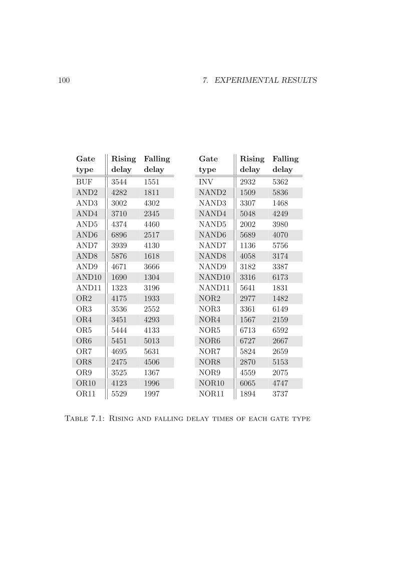
100 7. EXPERIMENTAL RESULTS
Gate Rising Falling
type delay delay
BUF 3544 1551
AND2 4282 1811
AND3 3002 4302
AND4 3710 2345
AND5 4374 4460
AND6 6896 2517
AND7 3939 4130
AND8 5876 1618
AND9 4671 3666
AND10 1690 1304
AND11 1323 3196
OR2 4175 1933
OR3 3536 2552
OR4 3451 4293
OR5 5444 4133
OR6 5451 5013
OR7 4695 5631
OR8 2475 4506
OR9 3525 1367
OR10 4123 1996
OR11 5529 1997
Gate Rising Falling
type delay delay
INV 2932 5362
NAND2 1509 5836
NAND3 3307 1468
NAND4 5048 4249
NAND5 2002 3980
NAND6 5689 4070
NAND7 1136 5756
NAND8 4058 3174
NAND9 3182 3387
NAND10 3316 6173
NAND11 5641 1831
NOR2 2977 1482
NOR3 3361 6149
NOR4 1567 2159
NOR5 6713 6592
NOR6 6727 2667
NOR7 5824 2659
NOR8 2870 5153
NOR9 4559 2075
NOR10 6065 4747
NOR11 1894 3737
Table 7.1: Rising and falling delay times of each gate type

101
PLST: This is the guaranteed time in picoseconds after which all paths inthe fault-free circuit have stabilised after modifying any primary orsecondary input.
TC: This is the clock sampling time in picoseconds. All experiments wererun setting TC to 1.2 times PLST.
O-FC: The measured optimistic fault coverage, i.e. the percentage of faultsthat were detected for at least one resistance.
FC: The measured fault coverage as defined in Section 6.4.
Time: This is the time in seconds which was needed to perform the simula-tion of all 100 test pairs on the machine mentioned above.
Memory peak: This is the highest amount of RAM (in MB) which thesimulator used at any time during the process.
The diagrams in Figures 7.1 and 7.2 show how the needed time andmemory depend on the number of simulated faults (in this case, also on thecircuit’s number of signals) and on the circuit’s depth, respectively. Theamount of needed time and memory clearly rises only linearly as the numberof treated faults rises. Meanwhile, there is no identifiable relation betweencircuit depth and use of computing resources.
The diagrams in Figures 7.3 and 7.4 show how the fault coverage dependson the number of simulated faults and on the circuit’s depth, respectively.The fault coverage values are uniformly distributed around their respectiveaverage values and the dispersion is not large.
Here, it was observed, that a fault coverage of slightly more than 50%was achieved with only 100 randomly generated test pairs. In order to learnmore about this topic a further experiment was performed on c5315 (secondlargest combinational circuit) and on s35932 (third largest sequential circuit).Two hundred random test pairs were simulated for each one of these twocircuits. The achieved fault coverage was measured after the simulation ofeach test pattern, in order to see how fault coverage depends on the numberof random test patterns. The diagrams in Figures 7.5 and 7.6 report theobtained results. In both cases, only about thirty to forty test pairs wereneeded to achieve a fault coverage of more than 60%. Furthermore, hundredtest patterns were enough to achieve a fault coverage of more than 70% (80%according to the optimistic metric).

102 7. EXPERIMENTAL RESULTS
Cir
cuit
Sig
nals
Fault
sD
epth
PLST
TC
O-F
C(%
)FC
(%)
Tim
eM
em
.peak
c0017
1122
517
508
2100
910
0.00
90.6
91
0.06
c0095
3264
620
820
2498
310
0.00
94.8
51
0.10
c0880
443
886
2611
6524
1398
2890
.86
78.4
714
0.94
c1908
913
1826
4220
9834
2518
0066
.05
56.1
740
1.77
c3540
1719
3438
4923
1594
2779
1264
.55
55.1
516
64.
17
c5315
2485
4970
5125
6032
3072
3891
.57
76.5
514
85.
68
c7552
3719
7438
4522
9785
2757
4185
.67
72.4
519
48.
76
s00027
1734
827
994
3359
297
.06
87.2
51
0.07
s00208
122
244
1350
849
6101
868
.04
59.2
34
0.27
s00298
136
272
1138
996
4679
579
.78
68.9
54
0.30
s00386
172
344
1351
161
6139
366
.57
60.3
35
0.36
s499
175
350
1461
399
7367
814
.29
12.5
05
0.36
s00382
182
364
1147
584
5710
074
.73
65.3
37
0.39
s00344
184
368
2291
337
1096
0489
.95
76.9
65
0.40
s00349
185
370
2291
337
1096
0489
.73
76.7
86
0.40
s00400
186
372
1147
584
5710
073
.39
64.0
96
0.40
s00444
205
410
1358
782
7053
864
.15
55.4
26
0.43
s00526
218
436
1138
996
4679
556
.43
48.8
47
0.46
s00510
236
472
1449
028
5883
380
.51
71.1
67
0.49
s00420
252
504
1559
199
7103
833
.14
29.2
08
0.51
s00832
310
620
1249
878
5985
343
.23
37.5
410
0.60
s00820
312
624
1249
878
5985
342
.95
37.3
210
0.62
s635
320
640
129
6071
3072
8555
31.4
125
.12
90.
62
Table 7.2: Experimental results: tabular overview

103
Cir
cuit
Sig
nals
Fault
sD
epth
PLST
TC
O-F
C(%
)FC
(%)
Tim
eM
em
.peak
s00641
433
866
7637
6483
4517
7981
.53
67.9
313
0.90
s00953
440
880
1872
860
8743
151
.60
44.2
414
0.86
s00713
447
894
7638
0275
4563
2978
.08
64.9
914
0.94
s00838
512
1024
1975
899
9107
813
.77
11.9
815
0.97
s938
512
1024
1975
899
9107
816
.80
14.7
116
0.97
s01238
540
1080
2410
4838
1258
0559
.36
49.9
916
1.04
s01196
561
1122
2611
7209
1406
5057
.40
48.1
117
1.06
s01494
661
1322
1977
886
9346
371
.94
64.0
320
1.22
s01488
667
1334
1977
886
9346
371
.97
64.1
021
1.26
s01423
748
1496
6126
1925
3143
0972
.00
58.2
424
1.52
s1512
866
1732
3212
9628
1555
5364
.38
53.8
127
1.71
s3271
1714
3428
3014
0204
1682
4488
.80
75.4
129
36.
63
s3384
1911
3822
6226
0511
3126
1392
.26
76.0
665
3.99
s3330
1961
3922
3113
6175
1634
0964
.03
54.3
861
3.70
s05378
2993
5986
2712
5531
1506
3763
.29
55.7
597
5.71
s09234
5844
1168
860
2812
0033
7439
43.6
136
.18
264
10.7
2
s13207
8651
1730
261
3046
3236
5558
57.0
646
.67
382
16.1
3
s15850
1038
320
766
8442
2286
5067
4362
.21
50.9
048
518
.96
s35932
1782
835
656
3115
3305
1839
6589
.47
78.3
773
336
.03
s38584
2071
741
434
5829
4145
3529
7373
.36
60.0
910
5138
.97
s38417
2384
347
686
4922
9613
2755
3577
.88
65.3
499
244
.21
AV
G:
2608
5216
33
150037
180044
67.1
657.7
6120
5.1
3
Table 7.3: Experimental results: tabular overview

104 7. EXPERIMENTAL RESULTS
9537 19074 28611 38148 47685 number of faults
time
memory peak
36
27
18
9210
420
630
840
451050
time mem.
(sec.) (MB)
Figure 7.1: Use of resources depending on number of faults
36
27
18
9210
420
630
840
451050
circuit depth26 52 78 104 130
time
memory peak
time mem.
(sec.) (MB)
Figure 7.2: Use of resources depending on depth of circuit

105
9537 19074 28611 38148 47685 number of faults
20
100
80
60
40
(%)
O−FC
FC
Figure 7.3: Fault coverage depending on number of faults
20
100
80
60
40
(%)
26 52 78 104 130 circuit depth
O−FC
FC
Figure 7.4: Fault coverage depending on depth of circuit

106 7. EXPERIMENTAL RESULTS
20 40 60 80 100 120 140 160 180 200number oftest pairs
20
40
60
80
100O−FC
FC
Figure 7.5: Fault coverage depending on number of test pairs,circuit c5315
20 40 60 80 100 120 140 160 180 200number oftest pairs
20
40
60
80
100O−FC
FC
Figure 7.6: Fault coverage depending on number of test pairs,circuit s35932
107
An interesting observation is made when analysing Figures 7.3 through7.6. The gap between O-FC and FC is rather small; in fact, O-FC neverexceeds FC by more than about 10 percentage points. This means that, inthe average, all faults which were detected for any resistance, could also bedetected for a large range of resistances.
An analysis of the simulator’s log files brought forth that all faults thatwere detected for any resistance had the range [Rmax, +∞[ in their C-ADI.Thus, ignoring that range for the computation of FC does not influence in anegative way the value FC (f) for any detected fault f .
Unfortunately, we are not aware of other authors having already proposeda similar simulator for resistive opens. Hence, it was not possible to comparethe obtained results with achievements of other authors.

108 7. EXPERIMENTAL RESULTS

8
Conclusions
Resistive opens are frequent defects in modern deep sub-micron technologies.They do not always affect the logic value of signal nodes, but cause signalchanges to delay. Although these delays may be small enough as to makethe fault hard-to-detect, it is very important to test for this kind of defects.
The resistance of an open is an unpredictable parameter, but it is essentialto characterise the behaviour of the defect. In this work, a simulator forresistive opens was designed and implemented. It computes each fault’sC-ADI, i.e. a set of ranges of resistances such that the open is detectedby the test set if its resistance is in one of those ranges. These simulationresults are especially useful during test pattern generation, as they tell if itis necessary to generate more test pairs that assure that the fault can bedetected for a wide range of resistances.
The simulator works in three Phases. All three phases were presented andthe method of Phase 1 was treated extensively. Additionally, possibilities ofmeasuring fault coverage based on ADI were discussed. A new fault coveragemetric was defined.
Experiments were performed on ISCAS 85 and ISCAS 89 circuits, the re-sults were reported. One conclusion was that the use of computing resourcesdepends only linearly on the circuit’s size.
Future work includes the integration of the technology-based delay-to-resistance mappings for Phase 2 of the RO-simulator, performance profilingand increasing interoperability with existing tools for static resistive bridgingfaults like that presented in [12].
109

110 8. CONCLUSIONS

Appendix A
Contents of the AttachedCD-ROM
Directory tree: Contents of directory:
Diplomarbeit|-- bin Makefile, README, executable files and| configuration files needed to compile| and run the simulator|-- include header files and documentation on| implemented classes|-- lib compiled library and object files|-- share| |-- Benchmarks benchmark files| |-- Documents support documents and some of the foreign| | works mentioned in the bibliography| |-- Experiments| | |--Inputs complete lists of faults and lists of| | | randomly generated test pattern pairs| | | used to perform the experiments| | ‘--Outputs complete lists of faults and log files| | generated by the experiments| ‘-- Thesis this document| ‘-- Sources pdfLATEX-sources| ‘-- Graphics included pdf-graphics‘-- src source files of main applications,
libraries and library testing routines
111

112 APPENDIX A. CONTENTS OF THE ATTACHED CD-ROM

Bibliography
[1] M. Abramovici, M.A. Breuer, A.D. Friedman. Digital systemstesting and testable design. Computer Science Press, 1990.
[2] R.C. Aitken. Nanometer technology effects on fault modelsfor IC testing. IEEE Transactions on Computer, vol. 32, no. 11,pp. 46-51, November 1999.
[3] B. Becker, I. Polian. Testen von digitalen ICs. Course held at theAlbert-Ludwigs-University of Freiburg, Winter Term 2003/04.
[4] M.L. Bushnell, V.D. Agrawal. Essentials of electronic testingfor digital, memory and mixed-signal VLSI circuits. KluwerAcademic Publishers, 2001.
[5] A. Campbell, E. Cole, C. Henderson, M. Taylor. Case history:failure analysis of a CMOS SRAM with an intermittentopen contact. 17th International Symposium for Testing and FailureAnalysis, Los Angeles, CA, November 1991.
[6] J.L. Carter, V.S. Iyengar, B.K. Rosen. Efficient test coveragedetermination for delay faults. Proceedings 1987 IEEE Interna-tional Test Conference, pp. 418-427, 1987.
[7] V.H. Champac, A. Zenteno. Detectability conditions for inter-connection open defects. IEEE VLSI Test Symposium, pp. 305-311, 2000.
[8] V.H. Champac, J. Figueras. Testability of floating gate de-fects in sequential circuits. Proceedings of the 13th IEEE VLSITest Symposium, pp. 202-207, 2005.
113

114 BIBLIOGRAPHY
[9] K.T. Cheng, A. Krstic. Current directions in automatic test-pattern generation. IEEE Transactions on Computer, vol. 32,no. 11, pp. 58-64, November 1999.
[10] R.D. Eldred. Test routines based on symbolic logical state-ments. Journal of the ACM, 6(1), pp. 33-36, 1959.
[11] P. Engelke, I. Polian, M. Renovell, B. Becker. Automatic test pat-tern generation for resistive bridging faults. Proceedings ofthe Ninth IEEE European Test Symposium, pp. 160-165, 2004.
[12] P. Engelke, I. Polian, M. Renovell, B. Becker. Simulating resistive-bridging and stuck-at faults. IEEE Transactions on Computer-Aided Design of Integrated Circuits and Systems, vol. 25, i. 10, pp. 2181-2192, October 2006.
[13] P. Engelke, I. Polian, M. Renovell, B. Seshadri, B. Becker. The prosand cons of very-low-voltage testing: an analysis based onresistive bridging faults. Proceedings of the 22nd IEEE VLSI TestSymposium, pp. 171-178, April 2004.
[14] J.M. Galey, R.E. Norby, J.P. Roth. Techniques for thediagnosing of switching circuit failures. Symposium on Switch-ing Circuit Theory and Logical Design, pp. 152-160, March 1961.
[15] C.D. Graas, H.A. Le, T.A. Rosi. Correlations between initialvia resistance and reliability performance. 35th Annual Pro-ceedings IEEE International Reliability Physics Symposium, April 1997.
[16] C. Hawkins, J. Soden, A. Righter, F.J. Ferguson. Defect classes -an overdue paradigm for CMOS IC testing. International TestConference, pp. 413-425, 1994.
[17] C.L. Henderson, J.M. Soden, C.F. Hawkins. The behavior andtesting implications of CMOS IC open circuits. InternationalTest Conference, pp. 302-303, 1991.
[18] K. Heragu, J.H. Patel, V.D. Agrawal. Segment delay faults: anew fault model. VLSI Test Symposium, pp. 32-39, 1996.

BIBLIOGRAPHY 115
[19] S. Irajpour, S.K. Gupta, M.A. Breuer. Multiple tests for eachgate delay fault: higher coverage and lower test appli-cation cost. Proceedings 2005 IEEE International Test Conference,pp. 9-17, November 2005.
[20] V.S. Iyengar, B.K. Rosen, J.A. Waicukauski. On computing thesizes of detected delay faults. IEEE Transactions on Computer-Aided Design of Integrated Circuits and Systems, vol. 9, no. 3, pp. 299-312, March 1990.
[21] N. Jha, S. Gupta. Testing of digital systems. CambridgeUniversity Press, 2003.
[22] H. Konuk. Voltage and current-based fault simulation forinterconnect open defects. Transactions On Computer-Aided De-sign of ICs and Systems, vol. 18, pp. 1768-1779, December 1999.
[23] C. Lee, D.M.H. Walker. PROBE: a PPSFP simulator for resis-tive bridging faults. VLSI Test Symposium, pp. 105-110, 2000.
[24] Z. Li, X. Lu, W. Qiu, W. Shi, D.M.H. Walker. A circuit level faultmodel for resistive opens and bridges. VLSI Test Symposium,pp. 379-384, 2003.
[25] J.C.M. Li, E.J. McCluskey. Testing for tunneling opens. Pro-ceedings of the International Test Conference 2000, pp. 85-94, 2000.
[26] E. Lindbloom, J.A. Waicukauski, B. Rosen, V. Iyengar. Transitionfault simulation by parallel pattern single fault propaga-tion. International Test Conference, pp. 542-549, 1986.
[27] A.K. Majhi, J. Jacob, L.M. Patnaik, V.D. Agrawal. On testcoverage of path delay faults. VLSI Design, pp. 418-421, 1996.
[28] A.K. Majhi, V.D. Agrawal. Tutorial: delay fault models andcoverage. VLSI Design, pp. 364-369, 1998.
[29] W. Maly. Realistic fault modeling for VLSI testing. DesignAutomation Conference, pp. 173-180, 1987.
[30] W. Maly, P.K. Nag, P. Nigh. Testing oriented analysis of CMOSICs with opens. Proceedings 1988 IEEE International Conference onComputer Aided Design, pp. 344-347, 1988.

116 BIBLIOGRAPHY
[31] E.J. McCluskey, C.W. Tseng. Stuck-fault tests versus actualdefects. International Test Conference, pp. 336-343, 2000.
[32] W. Needham, C. Prunty, E.H. Yeoh. High voltage microprocessortest escapes, an analysis of defects our tests are missing.Proceedings 1998 IEEE International Test Conference, pp. 25-34, Octo-ber 1998.
[33] E.S. Park et al. Statistical delay fault coverage and defectlevel for delay faults. Proceedings 1988 IEEE International TestConference, pp. 492-499, September 1988.
[34] I. Polian. On non-standard fault models for logic digi-tal circuits: simulation, design for testability, industrialapplications. VDI Fortschritt-Berichte, Reihe 20, Nr. 377, VDI-Verlag, Dusseldorf, 2004.
[35] A.K. Pramanick, S.M. Reddy. On the detection of delay faults.Proceedings 1988 IEEE International Test Conference, pp. 845-856,1988.
[36] A.K. Pramanick, S.M. Reddy. On the fault coverage of gatedelay fault detecting tests. IEEE Transactions on Computer-Aided Design of Integrated Circuits and Systems, vol. 15, no. 1, pp. 78-94, January 1997.
[37] M. Renovell, G. Cambon. Topology dependence of floatinggate faults in MOS integrated circuits. Electronics Letters,vol. 22, pp. 152-153, January 1986.
[38] M. Renovell, P. Huc, Y. Bertrand. CMOS bridge fault modeling.VLSI Test Symposium, pp. 392-397, 1994.
[39] M. Renovell, P. Huc, Y. Bertrand. The concept of resistanceinterval: a new parametric model for resistive bridgingfaults. VLSI Test Symposium, pp. 184-189, 1995.
[40] M. Renovell, F. Azaıs, Y. Bertrand. Detection of defectsusing fault model oriented test sequences. Journal of Elec-tronic Testing: Theory and Applications, 14:13-22, 1999.

BIBLIOGRAPHY 117
[41] M. Renovell, M. Comte, I. Polian, P. Engelke, B. Becker. Analyzingthe memory effect of resistive open in CMOS random logic.Design and Test of Integrated Systems in Nanoscale Technology 2006,pp. 251-256, September 2006.
[42] R. Rodrıguez-Montanes, E.M.J.G. Bruls, J. Figueras. Bridging de-fects resistance measurements in a CMOS process. Interna-tional Test Conference, pp. 892-899, 1992.
[43] R. Rodrıguez-Montanes, P. Volf, J. Pineda de Gyvez. Resistancecharacterization for weak open defects. IEEE Design & Test,v. 19 n. 5, p. 18-26, September 2002.
[44] G.L. Smith. Model for delay faults based upon paths.Proceedings 1985 IEEE International Test Conference, pp. 342-349,1985.
[45] J. Soden, R. Treece, M. Taylor, C. Hawkins. CMOS IC stuck-open fault electrical effects and design considerations.Proceedings 1989 IEEE International Test Conference, pp. 423-430,1989.
[46] C.W. Starke. Built-in test for CMOS circuits. International TestConference, pp. 309-314, 1984.
[47] N.N. Tendolkar. Analysis of timing failures due to random ACdefects in VLSI modules. Proceedings 22nd ACM/IEEE DesignAutomation Conference, pp. 709-714, June 1985.