afrl-ry-wp-tr-2009-1041afrl-ry-wp-tr-2009-1041 chip generators study mark horowitz, don stark, zain...
TRANSCRIPT

AFRL-RY-WP-TR-2009-1041
CHIP GENERATORS STUDY Mark Horowitz, Don Stark, Zain Asgar, Omid Azizi, Rehan Hameed, Wajahat Qadeer, Ofer Shacham, and Megan Wachs
Stanford University
DECEMBER 2008 Final Report
Approved for public release; distribution unlimited.
See additional restrictions described on inside pages
STINFO COPY
AIR FORCE RESEARCH LABORATORY SENSORS DIRECTORATE
WRIGHT-PATTERSON AIR FORCE BASE, OH 45433-7320 AIR FORCE MATERIEL COMMAND
UNITED STATES AIR FORCE

NOTICE AND SIGNATURE PAGE
Using Government drawings, specifications, or other data included in this document for any purpose other than Government procurement does not in any way obligate the U.S. Government. The fact that the Government formulated or supplied the drawings, specifications, or other data does not license the holder or any other person or corporation; or convey any rights or permission to manufacture, use, or sell any patented invention that may relate to them. This report was cleared for public release by the Defense Advanced Research Projects Agency (DARPA) and is available to the general public, including foreign nationals. Copies may be obtained from the Defense Technical Information Center (DTIC) (http://www.dtic.mil). AFRL-RY-WP-TR-2009-1041 HAS BEEN REVIEWED AND IS APPROVED FOR PUBLICATION IN ACCORDANCE WITH ASSIGNED DISTRIBUTION STATEMENT. *//Signature// //Signature//
ALFRED J. SCARPELLI BRADLEY J. PAUL, Chief Project Engineer Chief, Advanced Sensor Components Branch Advanced Sensor Components Branch Aerospace Components & Subsystems Aerospace Components & Subsystems Technology Division Technology Division Sensors Directorate //Signature//
TODD A. KASTLE Chief, Aerospace Components & Subsystems Technology Division Sensors Directorate This report is published in the interest of scientific and technical information exchange, and its publication does not constitute the Government’s approval or disapproval of its ideas or findings. *Disseminated copies will show “//Signature//” stamped or typed above the signature blocks.

i
REPORT DOCUMENTATION PAGE Form Approved
OMB No. 0704-0188
The public reporting burden for this collection of information is estimated to average 1 hour per response, including the time for reviewing instructions, searching existing data sources, searching existing data sources, gathering and maintaining the data needed, and completing and reviewing the collection of information. Send comments regarding this burden estimate or any other aspect of this collection of information, including suggestions for reducing this burden, to Department of Defense, Washington Headquarters Services, Directorate for Information Operations and Reports (0704-0188), 1215 Jefferson Davis Highway, Suite 1204, Arlington, VA 22202-4302. Respondents should be aware that notwithstanding any other provision of law, no person shall be subject to any penalty for failing to comply with a collection of information if it does not display a currently valid OMB control number. PLEASE DO NOT RETURN YOUR FORM TO THE ABOVE ADDRESS.
1. REPORT DATE (DD-MM-YY) 2. REPORT TYPE 3. DATES COVERED (From - To)
December 2008 Final 25 September 2008 – 31 December 2008 4. TITLE AND SUBTITLE
CHIP GENERATORS STUDY 5a. CONTRACT NUMBER
5b. GRANT NUMBER
FA8650-08-C-7829
5c. PROGRAM ELEMENT NUMBER
69199F 6. AUTHOR(S)
Mark Horowitz, Don Stark, Zain Asgar, Omid Azizi, Rehan Hameed, Wajahat Qadeer, Ofer Shacham, and Megan Wachs
5d. PROJECT NUMBER
ARPR 5e. TASK NUMBER
YD 5f. WORK UNIT NUMBER
ARPRYD07 7. PERFORMING ORGANIZATION NAME(S) AND ADDRESS(ES) 8. PERFORMING ORGANIZATION
Stanford University Computer Systems Laboratory Gates Building, Room 301 Stanford, CA 94305
REPORT NUMBER
9. SPONSORING/MONITORING AGENCY NAME(S) AND ADDRESS(ES) 10. SPONSORING/MONITORING AGENCY ACRONYM(S)
Air Force Research Laboratory Sensors Directorate Wright-Patterson Air Force Base, OH 45433-7320 Air Force Materiel Command United States Air Force
Defense Advanced Research Projects Agency/ Information Processing Techniques Office (DARPA/IPTO) 3701 North Fairfax Drive Arlington, VA 22203-1714
AFRL/RYDI
11. SPONSORING/MONITORING AGENCY REPORT NUMBER(S)
AFRL-RY-WP-TR-2009-1041
12. DISTRIBUTION/AVAILABILITY STATEMENT
Approved for public release; distribution unlimited.
13. SUPPLEMENTARY NOTES
PAO Case Number: DARPA 14146; Clearance Date: 08 Sep 2009. This report contains color.
14. ABSTRACT
This report explores a new way to think about designing digital systems, creating chip generators rather than chips, to resolve the crisis facing the chip industry: the need for high energy efficiency pushes us to create customized computing devices tailored to the user’s application, while the high cost of design pushes us to using generic computing solutions. Our research indicates that customized solutions can be orders of magnitude better, and that creating a chip generator requires changing the way we think and code hardware, but should be feasible.
15. SUBJECT TERMS
integrated circuits, VLSI, multi processors, design productivity, chip generator
16. SECURITY CLASSIFICATION OF: 17. LIMITATION OF ABSTRACT:
SAR
18. NUMBER OF PAGES
36
19a. NAME OF RESPONSIBLE PERSON (Monitor)
a. REPORT Unclassified
b. ABSTRACT Unclassified
c. THIS PAGE Unclassified
Alfred J. Scarpelli 19b. TELEPHONE NUMBER (Include Area Code)
N/A Standard Form 298 (Rev. 8-98)
Prescribed by ANSI Std. Z39-18

iii
Table of Contents
Section Page
List of Figures ..................................................................................................................................... iv
1 Summary ............................................................................................................................. 1
2 Introduction ......................................................................................................................... 2
3 Methods, Assumptions and Procedures .............................................................................. 5
4 Results and Discussion ........................................................................................................ 7
4.1 Performance Advantages of Customization ........................................................................ 7
4.2 Design Methodology for Creating Chip Generators ......................................................... 12 4.2.1 System on Chip Design ...................................................................................... 12 4.2.2 Higher-level Design Entry / Module Generation ............................................... 13 4.2.3 Capturing Design Knowledge ............................................................................ 13
4.3 Design Optimization ......................................................................................................... 15
4.4 Verification of a Chip Generator....................................................................................... 16 4.4.1 The Relaxed Scoreboard: Verifying a Reconfigurable System ......................... 17 4.4.2 Verifying a Generated Design ........................................................................... 20
5 Conclusions ....................................................................................................................... 23
6 Recommendations ............................................................................................................. 24
7 References ......................................................................................................................... 26
List of Acronyms, Abbreviations, and Symbols ................................................................................ 28

iv
List of Figures
Figure Page
1. Processor Energy versus Performance ...........................................................................3
2. Advantage of problem reformulation .............................................................................4
3. Diagram of the Smart Memory modular architecture ....................................................6
4. SIMD Extensions for computing integer motion estimation .........................................8
5. Custom Instructions and Datapaths ...............................................................................8
6. Customized memory system ..........................................................................................9
7. Area versus Performance for IME and FME ...............................................................10
8. Area for IME and FME ................................................................................................11
9. Energy for IME and FME ............................................................................................11
10. Simplified example of a module generator ..................................................................14
11. Overview of the design optimization framework ........................................................16
12. Difficulty in modeling memory system performance ..................................................18
13. Write atomicity violation .............................................................................................19
14. Relaxed scoreboard example .......................................................................................20

1
1 Summary Heterogeneous multicore systems hold the prospect of high energy efficiency, but are expensive to design, and often need to be customized for a particular application class. We explored one approach to reduce the design cost by creating a “chip generator”: a flexible, parameterized virtual device which can be tailored for each specific application. With a chip generator, the design process consists of configuring system parameters at a relatively high level based on the results of running the recompiled application on the modified target hardware. The application expert uses this process to tune both the algorithm and the hardware jointly to yield maximum performance. Once the tuning process is done, the generator creates the physical design and validation suite for the application optimized design. While creating a true multiprocessor chip generator will take a very large effort, our existing multicore design, with its extensible processors and flexible memory system, provided an ideal starting point to explore this approach. First, to validate the efficacy of creating tailored chips, we explored the efficiency advantage for customized hardware by porting real applications to our existing multicore system and examined how system efficiency can be improved by adding both generic and application specific hardware. Going through the complexity of building a multiprocessor chip generator only makes sense if the customized hardware solutions are much more energy efficient than non-application tuned approaches. While further work needs to be done, the preliminary results are very promising. Next we explored how to create a design description with input parameters that both permit an application designer to do efficient hardware/software tuning as well as producing efficient underlying hardware. In our preliminary work in this area, we realized that one of the key challenges that needs further research is how to compose many flexible sub-blocks into a larger flexible block. The challenge is bridging the gap between design parameters that the larger block wants to export to the application designer (or even higher level block), and the parameters of the internal sub-blocks. One approach that we have explored is to use optimization procedures to help create the actual implementation. Again our preliminary results have been very promising, but a much larger effort is needed to demonstrate this full technique. The final challenge that we explored in this project was how to create the validation collateral that is needed to test the customized design. Here we have demonstrated the power of using a “relaxed” scoreboard (SB), an output predictor that might not know the “right” answer, but knows that the answer must be in a small set of possible answers. This small additional flexibility makes it much easier to create flexible end-to-end checks. Chip generation provides a unified framework for many emerging trends in semiconductor design: (1) a focus on greater parallelism for energy efficiency (2) increasingly sophisticated hardware generators, including processors with extensible instruction sets that can be tailored for specific applications and (3) a tendency for successful semiconductor companies to build a family of devices in a given application class, each customized to be energy and cost efficient for a particular market sub-segment. By providing a framework that pulls together all these trends, the chip generator both allows application designers to make rapid, accurate hardware and software tradeoffs as well as reducing the marginal cost of each application-tailored design.

2
2 Introduction For over the past four decades, the semiconductor industry has been following Moore’s law, exponentially increasing the number of devices that can be integrated on a chip of silicon while growing the cost of that silicon chip slowly. To date, accompanying this decrease in cost have been corresponding increases in gate performance and decreases in gate power. Since the gates get faster and take less energy to operate, previous “big iron” systems fit on the desktop, and consumer mobile devices have the power of desktops of a few years ago. Just as important, it accomplished all this while not changing the underlying behavior of the transistors and wires by very much.1
[4]
Unfortunately, this lockstep scaling of cost, performance and power has broken down. While lithographic scaling will continue for at least another decade, we are only getting modest gains in performance or energy [10]. The gains that are being generated arise from technology changes that are not scalable, like strain and lower permittivity dielectrics: each generation requires new tricks to improve performance. Most problematic is power: while the number of gates doubles per generation, the switching energy per gate only decreases at best by about 0.7. A system in the new technology with the same clock frequency and twice the number of gates will have roughly 1.4 times the power unless the power density/gate is reduced. This power problem is one of the main reasons that uniprocessor performance has stopped scaling, forcing the computer industry to adopt multicore processors to enable continued power constrained performance scaling. Figure 1 plots the energy consumed by an instruction (Watts/SPEC) versus the peak performance of a processor, where the beneficial effects of technology scaling mentioned above have been normalized out. What one clearly sees is that as we have produced higher performance processors, the energy/instruction has also risen. We are operating at the steep part of the curve, where many watts/SPEC are spent to make the processors run a little faster. With multiple processors, you can make each processor slightly slower, which makes the core much more energy efficient, allowing more cores and higher total performance for the same power budget (for an power constrained design, the peak performance will be equal to the total power divided by the energy/op). This increase in energy efficiency by backing off on the peak performance is what is driving the move to multiple cores. Multiple cores, while being a critical technology, are not the final answer. Increasing the number of cores is useful in the steep portion of the energy-performance trade-off space, but, based on the historical data, the energy of each operation becomes a weak function of the processor speed once the design of the processor is targeted about 3 to 5 times below its peak performance. Beyond this point, there is no reason to make processors slower, and the power problem returns with increasing processor count.
1 There are many subtleties here, and there have been some issues with the relative speed of wires and transistors, and the increase in leakage currents. But these have been partially mitigated with technology changes, and have occurred slowly, so they have not caused a big change in design method.

3
Figure 1. Processor Energy versus Performance
Power/Spec2000 versus Spec2000 for Complementary metal–oxide–semiconductor (CMOS) processors shipped since 1984. The axes are corrected for the different technology. While these might not be power “optimal” designs, the energy versus performance curve has the expected diminishing returns shape. At low performance, there is not much change in energy as you lower performance; near the highest performance, there is not much change in performance for an increase in energy. If we are going to continue to scale processor performance we will need to make each of the cores more computationally efficient. Since efficient processor design has been a goal for at least the last decade (to forestall hitting the power wall) finding a generic energy efficient processor seems unlikely. In fact the most effective method of achieving energy efficiency is reformulating a task so it needs fewer operations to complete, as shown in Figure 2. This is the reason that digital signal processing (DSP) and vector units are more efficient than microprocessors for data parallel applications, and why specialized application-specific integrated circuits (ASIC) can be many orders of magnitude lower power than a microprocessor solution. The down-side of customized solutions is their very high design costs, running over $20M even for ASICs. This high cost is, in many ways, killing the whole ASIC industry. Thus we are currently facing a crisis in creating future computing devices: the need for high energy efficiency pushes us to create customized computing devices tailored to the user’s application, while the high cost of design pushes us to using generic computing solutions [7]. Our research in constructing chip generators, and not chips is one approach to resolving this dilemma.
Normalized Energy Vs. Normalized Performance
0.00 0.01 0.10 1.00 10.00Spec2006*L
Wat
ts /
( Spe
c200
6 * L
* Vd
d^2
)
intel 486intel pentiumintel pentium 2intel pentium 3intel pentium 4intel itaniumAlpha 21064Alpha 21164Alpha 21264SparcSuperSparcSparc64MipsHP PAPower PCAMD K6AMD K7AMD x86-64IBM PowerSUN UltraSPARCIntel Core 2AMD OpteronAMD PhenomIntel 386

4
Figure 2. Advantage of problem reformulation
A sketch of why problem reformulation is good for energy efficiency. If the new approach requires fewer operations for each task, it moves the optimal energy/performance trade-off curve down (there are less ops, so there is less energy dissipated), and to the right (each task takes less operations so if the operations remain at the same rate, the tasks/sec improves).
Energy/Task
User Performance

5
3 Methods, Assumptions and Procedures Our approach, like many solutions in computer science, is to add a level of indirection. Currently the tension is between the high design cost of custom solutions, and the high energy costs of generic processors. (Design and design validation dominate the fixed costs for a new design; mask tooling and prototype fabrication for a large digital system are generally only 10% of the total). What we really want is to create a very flexible (e.g., can change processor and memory resources, the number of processors, I/O configuration, etc) domain solution where the flexibility has very low cost. Since physically implementing this platform is impossible, we instead plan to create a highly flexible template that can create differently configured platform solutions. In this design study, we chose building multiprocessors as the application domain, since we already had infrastructure in this area. In other words we plan to create a virtual configurable multiprocessor, which can be optimized for the specific requirements of each set of applications, even to the point of adding some small amounts of application specific hardware. As application developers change chip parameters, the system would reconfigure and work to re-optimize the design, providing interactive feedback on the area/performance/energy implications of design choices. When the application developers have tuned their software and the hardware it runs on, the system would then generate the chip with little manual intervention. One way of viewing a multiprocessor chip generator is to imagine creating a very flexible architectural simulator that would allow one to change many of the design parameters in the machine using just a few knobs. Like some modern software/compiler optimization tools many of the detailed knobs (i.e., cache sizes, block sizes, banking, etc.) could be set by internal optimization passes as the user works at a higher level. While flexible architectural simulators have been in existence for quite a while, implementing a chip which matches the specification is an expensive exercise left for the designers. With a chip generator, once the user is happy with both the performance and power, she pushes a button and (possibly days later) a validated chip design database is produced. To help explore the potential benefits of creating a multiprocessor chip generator (in terms of energy and cost to reach a certain performance) and to develop a methodology to create one, we leveraged our previous Smart Memories design work [12], the chip multiprocessor research project recently performed under DARPA funding. The initial goal of the Smart Memories project was to build a more flexible computing platform that would be able to execute a range of different applications efficiently. The modular architecture, shown in Figure 3, incorporates flexibility both in its processing and memory components. The system consists of Tiles, each with two Tensilica cores [25] several reconfigurable memory blocks, and a crossbar connecting them. Tiles are placed in groups of four, forming Quads. Tiles in the Quad are connected to a shared protocol controller. The quad protocol controller is a programmable message engine that can perform all the required communication between the Tiles, from cache refills and cache coherence protocol to complex direct memory access (DMA) requests. Quads are then connected to each other and to the off-chip interfaces using an on-chip network.

6
Quad Quad Quad
Quad Quad Quad
Quad Quad Quad
-
Smart Memories
Crossbar
Tile
Tile Tile
Tile Tile
Prot
ocol
Con
trolle
r
Quad
Load/Store Unit
CPU CPU
Configurable MemoryMemory Controller
Mem
ory
Con
trolle
r
Mem
ory
Con
trolle
r
Memory Controller
Figure 3. Diagram of the Smart Memory modular architecture
Two Tensilica CPUs are connected through a crossbar to a number of configurable memory banks to form a tile. Four tiles plus a programmable memory controller create a quad.
While we had chosen configurable Tensilica processors for ease of implementation (they allowed us to create the specialized interfaces we needed to talk with our configurable memory system), they also allow us (or an application developer) to customize the processing capabilities to match the application demands. In addition, since the memory system was already built to be very flexible, it is possible to create new memory structures and protocols in our system. This architectural programmability permits Smart Memories to act as a very crude chip generator which we can use to explore the costs and advantages of customization. The data presented in this report was generated using the Smart Memory simulation system, and the Tensilica tool set. We used the Smart Memory simulation system to generate the performance estimates shown in the next section, and then used Tensilica tools to generate the Register Transfer Language (RTL) for the designs which we synthesized and then measured the area and power using Synopsys tools. We also used Synopsys tools (Vera) to generate some of the new test approaches described in the results section. The result of this study has been encouraging, and indicates more work needs to be done in this area. Starting with the Smart Memory design has another advantage as well. Since we have a complete design database for this chip and all the validation collateral, we can begin to explore other issues that need to be resolved for a multiprocessor chip generator. These include incorporating known optimization methods inside of the generator, creating the needed validation scripts for each instance generated, and creating a design methodology for creating a multiprocessor chip generator, rather than just an instance of a chip. During this short study, we have been able to look at one issue in each of these areas. This exploration has convinced us that building generators requires a different mindset and approach than building chips, and further study in this area is warranted.

7
4 Results and Discussion To explore the advantages and issues in creating a chip generator, we focused on four different sub-problems. Each will be explained in more detail in this section. The next section explores the potential advantage of using a chip generation approach. That is it tries to answer the question of what speedups/energy savings are possible using broad application optimizations, and then how much additional benefit is possible by using optimizations that might be tightly tied the application. Given the potential advantages of doing application optimization, Section 4.2 then looks at how can one create a chip generator – how should the generator be coded. This leads to the notion of using flexible components and code to create a more complex component. One attractive option in this framework is to create optimization routines that can be used on many different components. One such optimizer is explored in Section 4.3. The final problem that we attacked was that of validation, since it is the hardest problem a design team faces today. Here we think that a generator has a number of advantages over conventional System on Chip (SoC) design, since it allows the validation framework to be reused. To enable this reuse, we need to create checkers that can validate a wide range of implementations. Our solution to this issue, called a “relaxed” scoreboard is described in Section 4.4.
4.1 Performance Advantages of Customization The goal for this section of the research is to better understand why ASICs are so much more efficient than processors. What are the specific mechanisms that they use, and can these be copied to make our multiprocessors more efficient. The most interesting question is how custom tuned are each of these mechanisms, since we would like to evaluate the value of customization. If a small number of mechanisms handle most of the design efficiencies, then a flexible framework might be an essential tool to find these solutions, but, once found, these could be incorporated onto standard cores without the need for specialization. Another interesting question is to try to determine what parameters should be provided to the application designer. These have to be low level enough to give control of the machine, but high level enough to make software system support tractable. To examine efficiencies for a given application, our first step is to run that application on the Smart Memories base configuration of the machine with normal dual issue Tensilica processors. The next step is to add a “generic” hardware unit appropriate for this application (in many cases a short vector unit) by using the Tensilica Instruction Extension language (TIE) [11]. Then we try to further optimize this unit, adding small amounts of hardware, before looking at more radical TIE approaches that might be useful. By modifying the base Tensilica instruction set, we can add custom instructions and hardware blocks tailored to support a given application. We can also look at the performance, area, and power implications of tailoring the chip generator programmable memory hierarchy and communication paths for that application. Our first target application is H.264 video encoding which includes data and control intensive sub-algorithms, and has substantial compute requirements. For the initial study, we focused on

8
motion estimation. Given an image block, the estimator must find the closest match present in a reference image, a process that is very compute intensive. When implemented on the base Tensilica processor, integer motion estimation is about 600 times slower than required; it is very memory intensive and has 20% of its cycles nested in conditional code. With such a large performance gap, simply running multiple blocks in parallel on different cores would not be effective. A straightforward architectural improvement is to use Single Instruction, Multiple Data (SIMD) extensions, as shown in Figure 4. A 16 way SIMD, 2 Slot Very-Long Instruction Word (VLIW) architecture improves performance by a factor of 20 with an area overhead of 3x (110K gates versus 40K gates). Adding custom instructions and tailored data widths to this SIMD architecture (Figure 5) increases the performance gain to a factor of 70 with a slightly increased overhead (125K gates). The final 600x speedup can be reached by utilizing a more sophisticated data interconnection network, a wider datapath, and twice the register space (Figure 6). Tailoring the registers/memory is very effective, but it is also quite specialized to the function being optimized. Thus it seems like some customization is likely to be useful.
Figure 4. SIMD Extensions for computing integer motion estimation
This consists of adding a 16 way SIMD unit that can process 8bit video data.
Figure 5. Custom Instructions and Datapaths
Custom instructions for integer motion estimation greatly improve compute efficiency. Operations like the Sum of Absolute Difference (SAD), and conditional operations are very important.
9
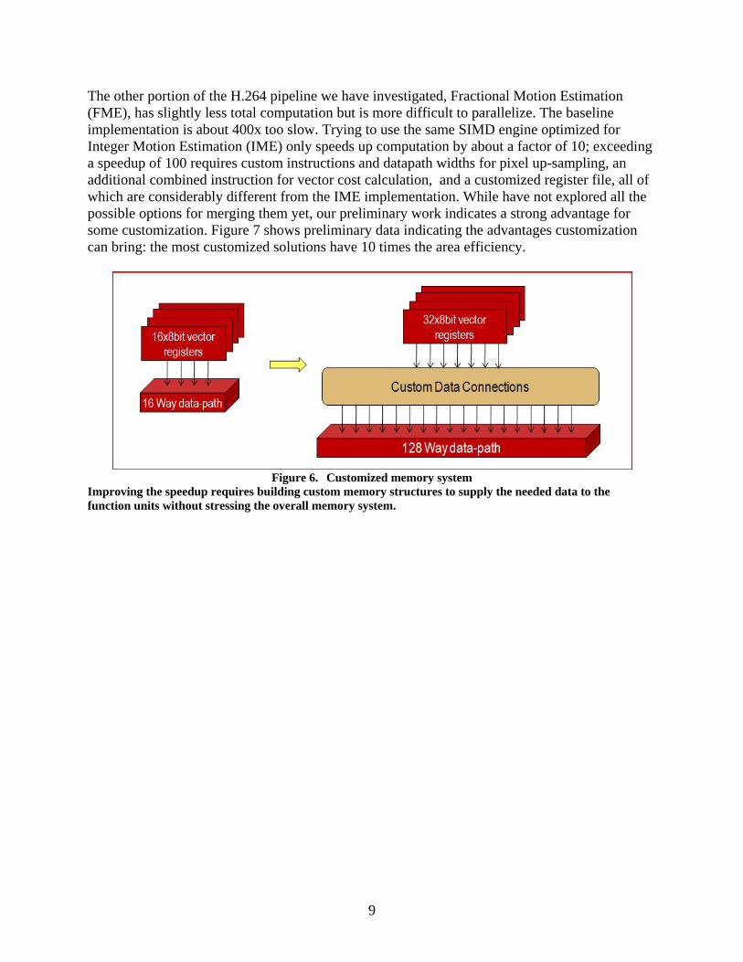
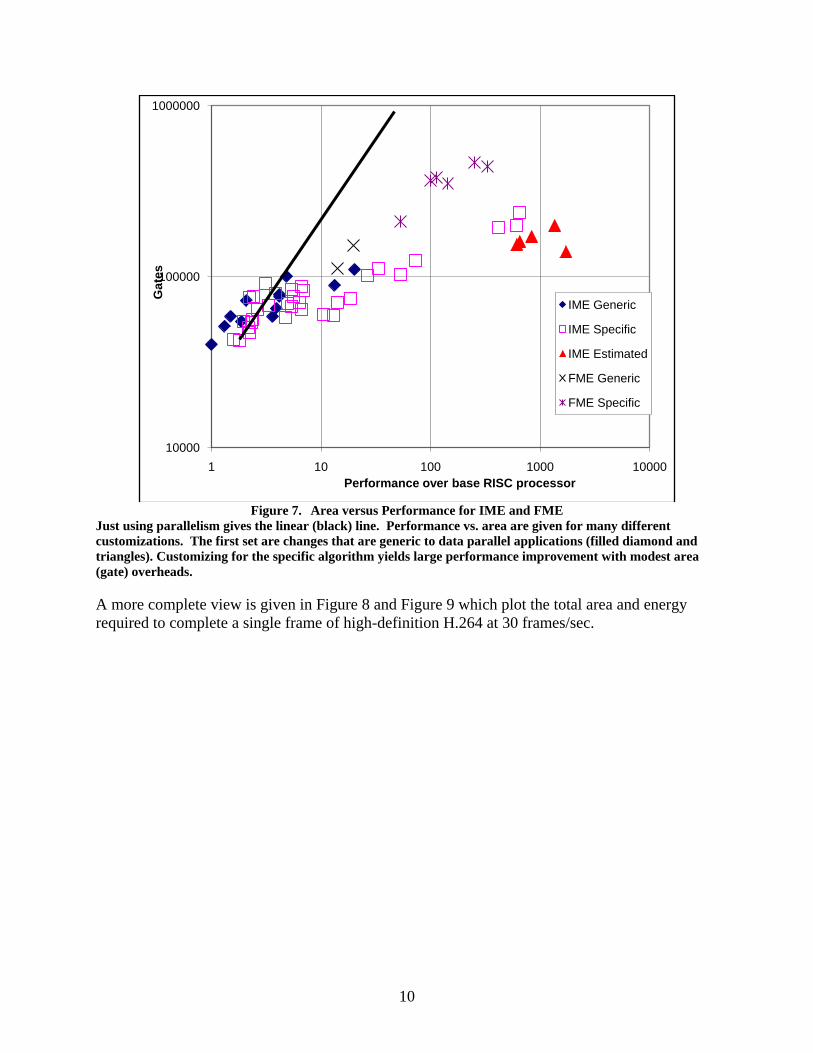
The other portion of the H.264 pipeline we have investigated, Fractional Motion Estimation (FME), has slightly less total computation but is more difficult to parallelize. The baseline implementation is about 400x too slow. Trying to use the same SIMD engine optimized for Integer Motion Estimation (IME) only speeds up computation by about a factor of 10; exceeding a speedup of 100 requires custom instructions and datapath widths for pixel up-sampling, an additional combined instruction for vector cost calculation, and a customized register file, all of which are considerably different from the IME implementation. While have not explored all the possible options for merging them yet, our preliminary work indicates a strong advantage for some customization. Figure 7 shows preliminary data indicating the advantages customization can bring: the most customized solutions have 10 times the area efficiency.
Figure 6. Customized memory system
Improving the speedup requires building custom memory structures to supply the needed data to the function units without stressing the overall memory system.
10
Figure 7. Area versus Performance for IME and FME
Just using parallelism gives the linear (black) line. Performance vs. area are given for many different customizations. The first set are changes that are generic to data parallel applications (filled diamond and triangles). Customizing for the specific algorithm yields large performance improvement with modest area (gate) overheads.
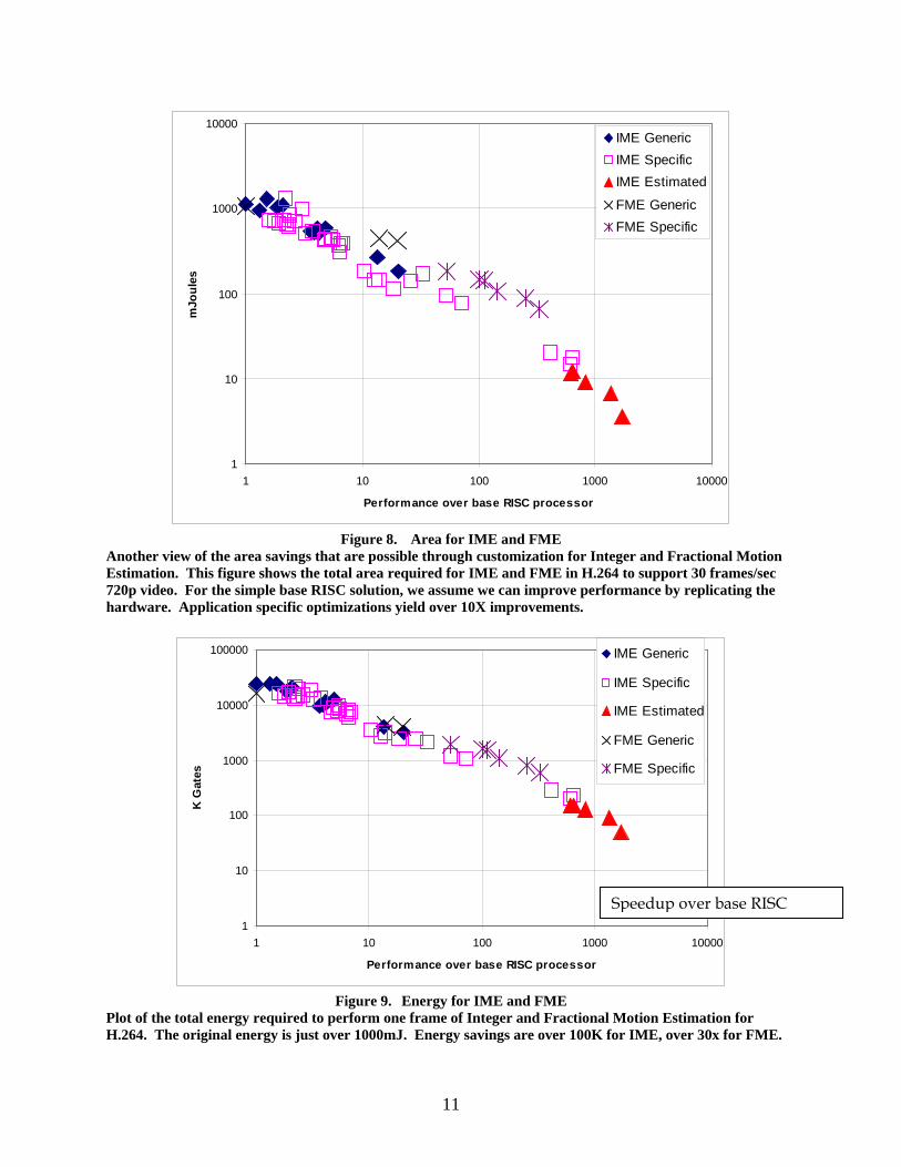
A more complete view is given in Figure 8 and Figure 9 which plot the total area and energy required to complete a single frame of high-definition H.264 at 30 frames/sec.
10000
100000
1000000
1 10 100 1000 10000
Gat
es
Performance over base RISC processor
IME Generic
IME Specific
IME Estimated
FME Generic
FME Specific
11
Figure 8. Area for IME and FME
Another view of the area savings that are possible through customization for Integer and Fractional Motion Estimation. This figure shows the total area required for IME and FME in H.264 to support 30 frames/sec 720p video. For the simple base RISC solution, we assume we can improve performance by replicating the hardware. Application specific optimizations yield over 10X improvements.
Figure 9. Energy for IME and FME
Plot of the total energy required to perform one frame of Integer and Fractional Motion Estimation for H.264. The original energy is just over 1000mJ. Energy savings are over 100K for IME, over 30x for FME.
1
10
100
1000
10000
1 10 100 1000 10000
Performance over base RISC processor
mJo
ules
IME GenericIME SpecificIME Estimated
FME GenericFME Specific
1
10
100
1000
10000
100000
1 10 100 1000 10000
Performance over base RISC processor
K G
ates
IME Generic
IME Specific
IME Estimated
FME Generic
FME Specific
Speedup over base RISC
12
While these results are promising, we need to extend this work to explore applications from a number of different problem domains. We have already started collaborating with John Shalf’s group at Lawrence Berkeley Laboratory, which is building a custom supercomputer for simulating climate. They have been using the Smart Memory simulator to investigate hardware and software tradeoffs and tuning [26].
4.2 Design Methodology for Creating Chip Generators Having shown the potential advantage for customizing the hardware, another major challenge this research explored was creating the flexible platforms that this design style requires. In this evaluation period we focused initially on how to specify the configurable substrate at the logical/functional level. This work built on the rich set of ideas from two current research communities – those on creating higher-level design entry languages, such as System Verilog [23], Bluespec [3] and electronic system languages (ESL) like Catapult C [24], and those groups creating flexible components, like Tensilica [25], Sonics [19], and Spiral [20]. We have also experimented with our configurable Smart Memory design to better understand trade-offs between possible approaches to creating a flexible generator. This work helped us understand what would need to be done to allow us to capture more designer knowledge, and in a future effort we will continue to refine this understanding and create and demonstrate a system that implements these ideas.
4.2.1 System on Chip Design The introduction of logic synthesis and the acceptance of Verilog/VHDL as the main design entry languages enabled a major leap in designer productivity. There has been much work on trying to repeat this success by moving design to higher level abstractions. Rich libraries of components have been created for designers to use, like the DesignWare library from Synopsys [22] or the component library in the Xilinx design system [27]. While the designer still works in a Verilog-like language, the components they are using are becoming larger and more complex. Designers no long worry about how to build simple functional units like adders or multipliers; they leave those issues to the library designer. A number of years ago it was felt that the rising availability and complexity of system blocks would lower the cost of designs which collected a number of these parts to create SoC designs. While these blocks did make the creation of complex systems simpler, the difficulty of validation remained related to the overall complexity of the chip and continued to require larger teams to address. Even if each of the blocks was previously validated, the designer needs to ensure that they interoperate in the chip environment. Since the interaction between the blocks is different for each use, eliminating subtle bugs requires an expensive custom validation effort. Our work on creating a multiprocessor generator addresses this issue by “fixing” the top level system architecture. Communication pathways will be specified in the design in a configurable fashion. Rather than allowing the designers to change the connections between blocks, we will allow them to configure the blocks (and the properties of the interconnections). Since we control all the possible interactions, we will be able to generate the test vectors and checkers needed to validate each generated multiprocessor configuration.

13
4.2.2 Higher-level Design Entry / Module Generation Another approach to improve designer productivity is to up-level the design input language. Languages like System Verilog [23] take a small step, but are widely used. Blue-spec [3] goes further by providing the designer a guarded/action model of hardware design. While these languages are clearly needed steps, they don’t directly enable one to create flexible hardware implementations. In a few restricted application domains, researchers have created even higher level design entry systems. For example, there are a few groups that have created a Simulink to chip flow [28] that works well for signal processing applications. The recent hardware Spiral effort at CMU [20] goes one step further, taking a fairly high-level description of a signal processing algorithm and creating an optimized hardware implementation. For applications with data parallelism, Synfora [21] generates hardware from a restricted set of input “C” code. If you view the input to these tools as input parameters, these tools can be viewed as a kind of module generator, with the starting code acting as a set of input parameters. The idea of creating generators is not a new idea; there are numerous commercial versions. Most of the embedded processor companies, including ARM [1], MIPS [15] and Tensilica [24], have systems that allow a user to extend the instruction set of the processor. With Tensilica, for example, the user provides a register transfer description of the desired operations, including the internal states needed for the instruction, and the tool generates the necessary hardware and software system support. Generators are also available for functions other than processing; Sonics [19] has created similar tools for on-chip interconnection interconnections. The user specifies the logical interconnections between units on the chip, including bandwidths and latency requirements, and the tool will generate the hardware. There are two main reasons why neither the current domain specific generation tools nor the current generators are sufficient to create the multiprocessor generator. First, since each only works for restricted domains, they at best will create modules for the overall generator. There needs to be a larger framework which satisfies the specific assumptions about input and output data on which these modules rely. Second, since these tools will produce modules that interact with one another, there will be interrelated constraints on their input parameters. In some cases, parameters for the tool will be completely derived from other higher-level parameters. One of the key research questions is how to create a system where the parameters for higher-level blocks are not simply the concatenation of all the parameters of constituent lower level modules. Our proposed approach is associate a program with each flexible module which computes the lower-level parameters from parameters for that module.
4.2.3 Capturing Design Knowledge In order to create a multiprocessor generator that allows customization with little effort, the framework must capture more than the function units and their interconnections. Even if both are flexible, there is often a tremendous amount of design knowledge needed to understand how to set the “parameters” of these units to yield efficient execution. So while we want to give the application designer control of the hardware that is generated, we need to give them that control at a level that they understand. For example over the years we have created a number of

14
different coherence and memory ordering rules. Each of these require a specific set of hardware and protocol rules for correct implementation, and often contain a number of tricky corner cases. The generator for the tile might contain a parameter that specifies the desired coherence, which in turn generates the specific hardware/operations needed to implement it. A more interesting example is to incorporate the notion of embedded optimization in the generator. At the circuit level there have been a number of tools for optimally sizing transistors and Vdd to yield the most energy efficient designs [17]. Recent work in our group and others' have looked at extending this optimization to include optimization of microarchitectural features [15]. Such an optimizer could set many of the processor memory system design parameters (i.e., block size, associativity, memory bandwidth) once the application workload is known. Building this type of optimizer is explored in the next section. The simplest way of creating module generators that incorporate this type of knowledge is to write a program that generates the desired hardware directly from the parameters. We feel this approach is probably optimal for smaller blocks, but will not scale well. First, the complexity of the generator increases rapidly as the complexity of the hardware increases. Since there is a program which generates the hardware, the code is often hard to debug, making it very difficult to create correct generators. Second, this solution essentially creates monolithic blocks, which does not allow one to leverage the design work of others in creating the generator. We plan to use this type of fused hardware/program generator for the lowest level blocks. For higher level blocks, we plan to use the scheme shown in Figure 10, which consists of a set of blocks and a piece of code that describes how the parameters of the included blocks should be computed from the higher level parameters. Our assumption is that similarly to hardware modules, there will be common optimization functions that will be reused in a number of the modules in the design.
Figure 10. Simplified example of a module generator
A conceptual example of a modular generator. It will consist of an interconnection of configurable modules, and a program that describes how to generate the parameters for the included modules.
Our preliminary effort demonstrated that this is a challenging problem and further work is needed in this area. In a future effort we plan to explore this problem from two angles. To create concrete examples, we will start recoding the design of the current Smart Memory tile, both
Tile Generator
CPU GeneratorParams: width…
Params: num_cpus, shared_caches, memory_model, …
CPU GeneratorParams: width…
Load-Store-Unit Generator
Params: depth, bandwidth…
Cache GeneratorParams: assoc’…
CPU GeneratorParams: assoc’…
Tile ProgramTile 0:
Cache 0:type = DATA;size = 16K; assoc = 2;
Cache 1:type = INST;size = 16K;assoc = 4;
CPU 0:…Connectivity:…
Tile Generator
CPU GeneratorParams: width…
Params: num_cpus, shared_caches, memory_model, …
CPU GeneratorParams: width…
Load-Store-Unit Generator
Params: depth, bandwidth…
Cache GeneratorParams: assoc’…
CPU GeneratorParams: assoc’…
Tile Generator
CPU GeneratorParams: width…
Params: num_cpus, shared_caches, memory_model, …
CPU GeneratorParams: width…
Load-Store-Unit Generator
Params: depth, bandwidth…
Cache GeneratorParams: assoc’…
CPU GeneratorParams: assoc’…
Tile ProgramTile 0:
Cache 0:type = DATA;size = 16K; assoc = 2;
Cache 1:type = INST;size = 16K;assoc = 4;
CPU 0:…Connectivity:…

15
making it more general and incorporating more designer information about how the underlying parameters should be set. This process will also help us understand which conceptual models and constraints work best in building a chip microprocessor generator. We will also need to address how one incorporates external IP used in the design.
4.3 Design Optimization One of the critical tasks in building a generator is to determine, given the parameters at a higher level of abstraction, how to set the parameters of the lower-level modules. While some of this task will be very application specific, there is also the generic task of finding the parameters that “optimize” the performance of the unit, along the axes that are important to the higher level module (power, throughput, latency, area). The designer may be seeking to maximize performance within a power budget, as is the case for high performance chips; to minimize power consumption while meeting some performance target, as is the case for embedded devices; or to optimize some other combination of requirements on performance, power and/or area. Given the importance and universality of this type of optimization, it is a critical part of our chip generation research. This design optimization problem is essentially a trade-off analysis problem: each design parameter in the system can be used to increase performance, but usually comes with an associated cost in terms of additional area and/or power. For example, to increase the performance of a particular design, the design optimizer may be able to increase cache size, to use a deeper pipeline with a higher clock frequency, to use a lower latency functional unit in some critical part of the design, etc. All of these choices, however, would increase both area and power consumption. The optimization challenge, therefore, is to make choices that would make the most efficient use of the available resources. Thus, we note that to optimize for efficiency, we are really looking for those design choices that have the lowest cost per unit performance. We can formalize this notion by defining the marginal cost of a design choice, shown here for energy-performance optimization:
Marginal Cost = PE
∆∆
. (E: energy, P: performance) (1)
With marginal costs in hand, the optimization phase then becomes a procedure of "selling" those design options with high costs, and "buying" those design options with lower costs. While this idea works, the challenge lies in creating the design space models that define how a change in a design parameter affects the performance, power and area characteristics of the system. Without these models, we cannot compute the desired marginal costs, and cannot perform the optimization. Usually, this modeling is done through architectural simulation. The complex nature of a chip architecture, along with the interactions between the architecture and the application code, usually requires that architectural simulators be used. The large multi-dimensional design space and long simulation times, however, make conventional simulation prohibitive for design space exploration. Fortunately, there have been advances in modeling such large architectural spaces by using sampling and statistical inference techniques [30][31]. In our approach, we can rely on similar techniques to do our architectural modeling.

16
While we can perform architectural modeling to determine the architectural characteristics of the chip, determining the actual power consumption and area usage of the chip requires knowledge of the underlying circuit characteristics. For example, if an architecture calls for a high-speed adder, we need to know the energy consumption per operation of that adder. Moreover, a high-speed adder will consume more power than a less aggressively designed lower-speed adder, so there is also a trade-off in the design space of the underlying circuits. Thus, to generate a truly optimized chip, we need to consider all levels of the design hierarchy—including both the trade-offs in the architectural design space and the trade-offs in the circuit design space. To optimize across both these design spaces, we propose the optimization framework in Figure 11. For each basic circuit block of the architecture, we map out the design trade-offs and store this information in a circuit trade-off library. We then create architectural models using simulation and statistical techniques. We couple these models together inside an optimization module which then finds the best set of design parameters.
Figure 11. Overview of the design optimization framework
Circuit design trade-offs for building blocks circuits are characterized and stored in the circuit trade-offs library. Architectural models map how higher-level architectural parameters affect performance. This information is fed to an optimizer which then selects the best set of design parameters.
A first version of this methodology has already been used to perform area-performance optimization for chip multiprocessor (CMP) designs [29]. This solution is an instance of a general approach to solve most performance/energy/area/cost optimization problems. All it requires is a simulation model that can evaluate architectural trade-offs, and an ability to extract a convex model of the sampled simulation results, and a set of circuit trade-off of the underlying circuit libraries. We expect that incorporating this type of optimization in the chip generator approach will allow it to produce optimized energy/cost for the desired level of performance.
4.4 Verification of a Chip Generator We do not expect to produce a bug-free generator, and we doubt that anyone would believe us if we asserted that we had created such a thing. Therefore, an essential aspect of this research was enabling the validation of the generated designs. We do not expect our tool to automatically validate the generated designs, but we do expect it to automatically generate what we already use: testbenches, test vectors, assertions, and reference models. Test vectors must either be self-

17
checking, or use a reference model to check the design behavior. Directed test cases are limited in how strenuously they can test the design, because the test writer needs to predict the exact, correct result of the tests. In order to achieve high coverage of the design state space, we actually want to have the ability to apply any input to the design and declare that it is behaving correctly, in a wide variety of scenarios. The usual way to achieve this goal is to create a reference scoreboard, or “golden model” of the design. Then the verification engineer can apply stimuli, including completely random stimuli, to both the design and to the golden model. However, even in a non-reconfigurable system, constructing a golden model of the design is a non-trivial task. Generally, design specifications (such as shared memory protocols) specify rules and axioms that are easier to describe by a non-deterministic state machine— they do not completely specify the memory system’s behavior. As a result, a design may have multiple correct implementations that perform differently, and thus need different golden models. This coupling causes two problems. First, one needs to create a new golden model for each implementation, and second, it is hard to keep the validation model completely separate from the implementation, which can lead to correlated errors. In the next section we describe how we dealt with this problem in verifying the Smart Memories system, then how we will extend our solution for the Chip Generator.
4.4.1 The Relaxed Scoreboard: Verifying a Reconfigurable System In verifying the Smart Memories system, we wrote assertions which held regardless of the configuration of the design, and software test cases that were applied at a high enough level that the exact system configuration was irrelevant. However, we wanted to create a reference model for the design that could be used unchanged across many configurations of the design. As explained above, creating a golden model for even a single design is a difficult and problematic task, and the reconfigurability in the Smart Memories system only increased the difficulty. In order to understand the difficulty in verifying a complicated system, such as a shared memory system, consider the simple example shown in Figure 12. In this four-processor system, processors 1, 2 and 3 are initiating writes to address a while processor 4 is reading the value saved at that address. The data is returned some time after the load started, as noted by the curved arrow. Depending on the exact arbitration mechanism, each of the values 1, 2 or 3 might be returned as the result of the load instruction.
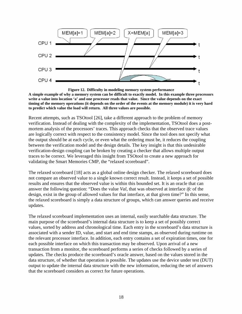
18
Figure 12. Difficulty in modeling memory system performance
A simple example of why a memory system can be difficult to exactly model. In this example three processors write a value into location ‘a’ and one processor reads that value. Since the value depends on the exact timing of the memory operations (it depends on the order of the events at the memory module) it is very hard to predict which value the load will return. All three values are possible.
Recent attempts, such as TSOtool [26], take a different approach to the problem of memory verification. Instead of dealing with the complexity of the implementation, TSOtool does a post-mortem analysis of the processors’ traces. This approach checks that the observed trace values are logically correct with respect to the consistency model. Since the tool does not specify what the output should be at each cycle, or even what the ordering must be, it reduces the coupling between the verification model and the design details. The key insight is that this undesirable verification-design coupling can be broken by creating a checker that allows multiple output traces to be correct. We leveraged this insight from TSOtool to create a new approach for validating the Smart Memories CMP, the “relaxed scoreboard”. The relaxed scoreboard [18] acts as a global online design checker. The relaxed scoreboard does not compare an observed value to a single known correct result. Instead, it keeps a set of possible results and ensures that the observed value is within this bounded set. It is an oracle that can answer the following question: “Does the value Val, that was observed at interface ifc of the design, exist in the group of allowed values for that interface, at that given time?” In this sense, the relaxed scoreboard is simply a data structure of groups, which can answer queries and receive updates. The relaxed scoreboard implementation uses an internal, easily searchable data structure. The main purpose of the scoreboard’s internal data structure is to keep a set of possibly correct values, sorted by address and chronological time. Each entry in the scoreboard’s data structure is associated with a sender ID, value, and start and end time stamps, as observed during runtime on the relevant processor interface. In addition, each entry contains a set of expiration times, one for each possible interface on which this transaction may be observed. Upon arrival of a new transaction from a monitor, the scoreboard performs a series of checks followed by a series of updates. The checks produce the scoreboard’s oracle answer, based on the values stored in the data structure, of whether that operation is possible. The updates use the device under test (DUT) output to update the internal data structure with the new information, reducing the set of answers that the scoreboard considers as correct for future operations.

19
Overall, the relaxed scoreboard is essentially a set of global protocol-level assertions. The assertions are constructed to verify that certain rules of the protocol are followed at a high level, without actually relying on or examining the implementation details. As an example, let us examine how a relaxed scoreboard would check for write atomicity, which is part of many consistency models. In order to detect write atomicity violations, we convert the protocol property into a check and update operation, and add these operations to the functions that the relaxed scoreboard performs: PROTOCOL PROPERTY: All processors see writes to the same location in the same order: single serialization point. If there is a store that is observed by one processor, it should be observed as completed by all processors. CHECK: A load can only return a value which was valid at some point between its start-of-interval and end-of-interval. UPDATE: When one processor loads a value from a certain location, mark all previously committed stores to this location as invalid after the load time. Using this rule can find the write atomicity violation shown in Figure 13:
Time P1 P2 P3 P4 P5 10 WR(a,1) WR(a,2) nop nop nop 20 nop Nop RD(a,1) nop nop 30 nop Nop nop RD(a,2) nop 40 nop Nop nop nop RD(a,1)
* Assume MEM[a]=0 at time 0 ** Assume read operations complete in less than 10 cycles
Figure 13. Write atomicity violation This figure show the memory operations of 5 processors . At time 10, P1 writes locations a with a the value 1, while P2 writes the same location with the value 2. While P3 and P4 reads might be correct, there are no orderings possible where P5 read is correct.
In this example, Processors 3, 4, and 5 disagree on the ordering of the store to address a. Figure 14 illustrates the operation of the relaxed scoreboard for the above code sequence. The top part shows portions of the specification’s non-deterministic state machine that correspond to the code above. It shows that one of two sequences can exist: either P1 wrote 1 and then P2 wrote 2 or vice versa—write atomicity is maintained in both cases. The portion of the figure that is drawn in bold illustrates the implementation’s deterministic state machine. The bottom part of the figure shows the state of the relaxed scoreboard with respect to the same code. The scoreboard identifies two writes and marks both values as possible answers. This corresponds to the state machine being in either state Init, A, B, C or D. When the first read is reported to the scoreboard, the scoreboard deduces that the design can be in either state A, B or D, and when the second read is reported, the uncertainty window collapses to a single allowed value. In this example, the scoreboard will immediately identify the read by processor 5 as an error since the returned value is no longer in its list of allowed values for that address.
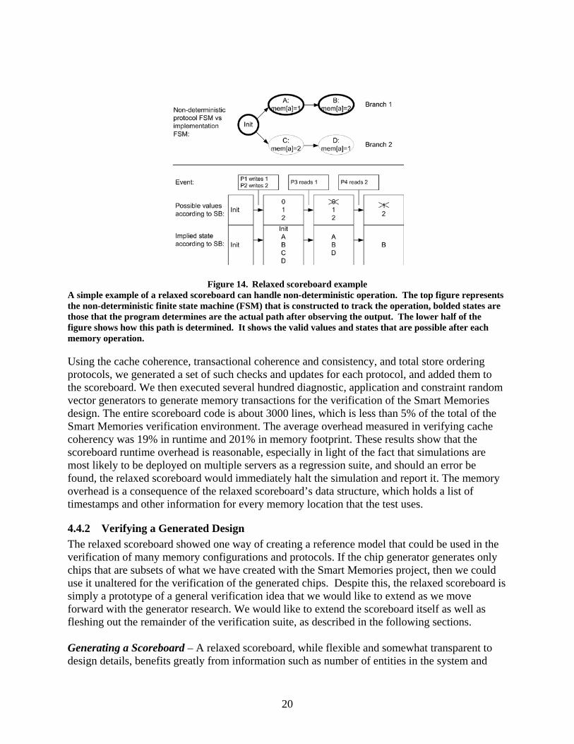
20
Figure 14. Relaxed scoreboard example A simple example of a relaxed scoreboard can handle non-deterministic operation. The top figure represents the non-deterministic finite state machine (FSM) that is constructed to track the operation, bolded states are those that the program determines are the actual path after observing the output. The lower half of the figure shows how this path is determined. It shows the valid values and states that are possible after each memory operation.
Using the cache coherence, transactional coherence and consistency, and total store ordering protocols, we generated a set of such checks and updates for each protocol, and added them to the scoreboard. We then executed several hundred diagnostic, application and constraint random vector generators to generate memory transactions for the verification of the Smart Memories design. The entire scoreboard code is about 3000 lines, which is less than 5% of the total of the Smart Memories verification environment. The average overhead measured in verifying cache coherency was 19% in runtime and 201% in memory footprint. These results show that the scoreboard runtime overhead is reasonable, especially in light of the fact that simulations are most likely to be deployed on multiple servers as a regression suite, and should an error be found, the relaxed scoreboard would immediately halt the simulation and report it. The memory overhead is a consequence of the relaxed scoreboard’s data structure, which holds a list of timestamps and other information for every memory location that the test uses.
4.4.2 Verifying a Generated Design The relaxed scoreboard showed one way of creating a reference model that could be used in the verification of many memory configurations and protocols. If the chip generator generates only chips that are subsets of what we have created with the Smart Memories project, then we could use it unaltered for the verification of the generated chips. Despite this, the relaxed scoreboard is simply a prototype of a general verification idea that we would like to extend as we move forward with the generator research. We would like to extend the scoreboard itself as well as fleshing out the remainder of the verification suite, as described in the following sections. Generating a Scoreboard – A relaxed scoreboard, while flexible and somewhat transparent to design details, benefits greatly from information such as number of entities in the system and
21
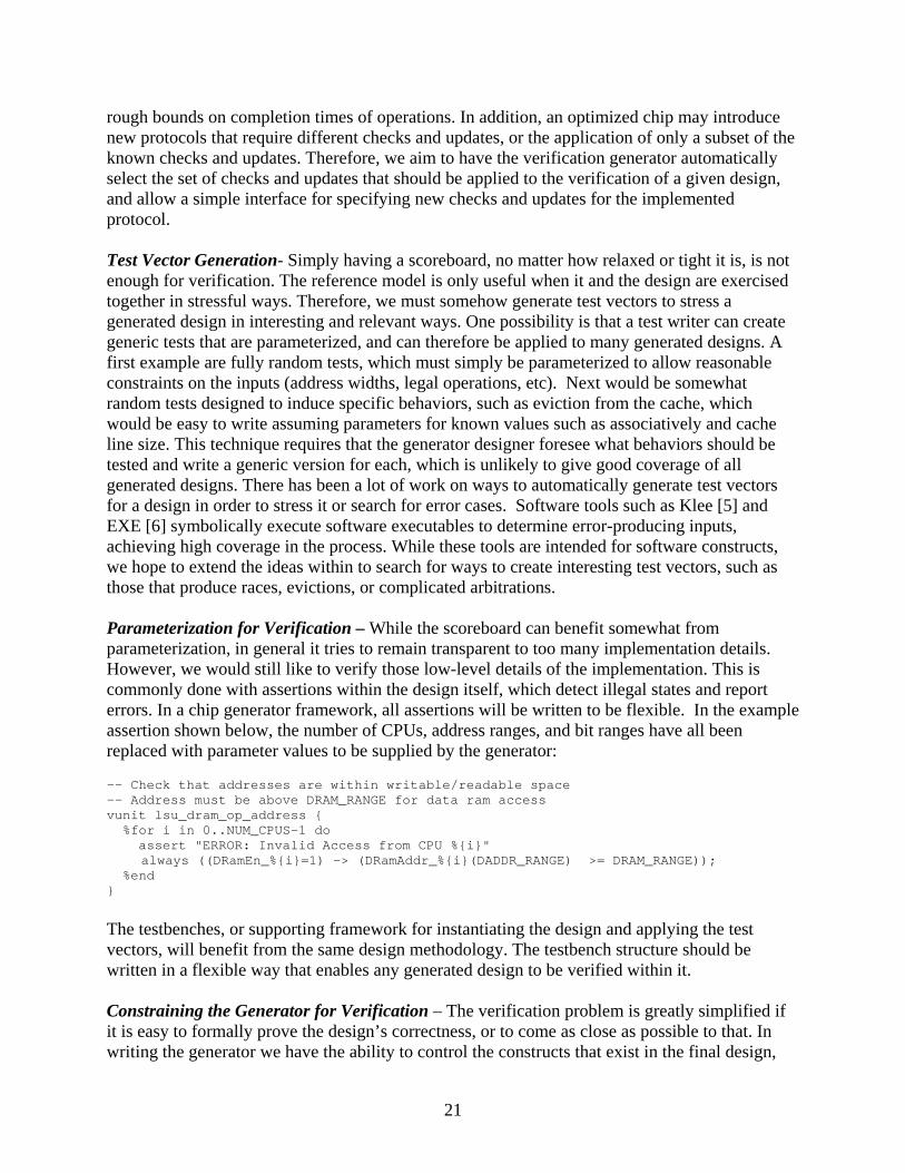
rough bounds on completion times of operations. In addition, an optimized chip may introduce new protocols that require different checks and updates, or the application of only a subset of the known checks and updates. Therefore, we aim to have the verification generator automatically select the set of checks and updates that should be applied to the verification of a given design, and allow a simple interface for specifying new checks and updates for the implemented protocol. Test Vector Generation- Simply having a scoreboard, no matter how relaxed or tight it is, is not enough for verification. The reference model is only useful when it and the design are exercised together in stressful ways. Therefore, we must somehow generate test vectors to stress a generated design in interesting and relevant ways. One possibility is that a test writer can create generic tests that are parameterized, and can therefore be applied to many generated designs. A first example are fully random tests, which must simply be parameterized to allow reasonable constraints on the inputs (address widths, legal operations, etc). Next would be somewhat random tests designed to induce specific behaviors, such as eviction from the cache, which would be easy to write assuming parameters for known values such as associatively and cache line size. This technique requires that the generator designer foresee what behaviors should be tested and write a generic version for each, which is unlikely to give good coverage of all generated designs. There has been a lot of work on ways to automatically generate test vectors for a design in order to stress it or search for error cases. Software tools such as Klee [5] and EXE [6] symbolically execute software executables to determine error-producing inputs, achieving high coverage in the process. While these tools are intended for software constructs, we hope to extend the ideas within to search for ways to create interesting test vectors, such as those that produce races, evictions, or complicated arbitrations. Parameterization for Verification – While the scoreboard can benefit somewhat from parameterization, in general it tries to remain transparent to too many implementation details. However, we would still like to verify those low-level details of the implementation. This is commonly done with assertions within the design itself, which detect illegal states and report errors. In a chip generator framework, all assertions will be written to be flexible. In the example assertion shown below, the number of CPUs, address ranges, and bit ranges have all been replaced with parameter values to be supplied by the generator: -- Check that addresses are within writable/readable space -- Address must be above DRAM_RANGE for data ram access vunit lsu_dram_op_address { %for i in 0..NUM_CPUS-1 do assert "ERROR: Invalid Access from CPU %{i}"
always ((DRamEn_%{i}=1) -> (DRamAddr_%{i}(DADDR_RANGE) >= DRAM_RANGE)); %end }
The testbenches, or supporting framework for instantiating the design and applying the test vectors, will benefit from the same design methodology. The testbench structure should be written in a flexible way that enables any generated design to be verified within it. Constraining the Generator for Verification – The verification problem is greatly simplified if it is easy to formally prove the design’s correctness, or to come as close as possible to that. In writing the generator we have the ability to control the constructs that exist in the final design,

22
and can control how difficult they are to verify. [13] describes a methodology for quickly determining, early in the design process, what aspects of a design may be difficult to verify. We can apply this methodology to both generic, high-level products of the generator as well as the specific implementations it creates, to give feedback to the generator designers on better constructs to use to enable verification.

23
5 Conclusions The new scaling rules for CMOS technology have created a conundrum – to increase performance will require creating more energy efficient designs, but high design cost currently prevent people from customizing their designs to provide the needed efficiency. We propose to address these issues by exploring the creation of domain-specific chip generators, which can create application optimized solutions at low design costs. Like the move to ASICs in the 1980’s, moving to a chip generator solution will again make application specific chips a viable alternative. While this seems like a promising approach, there are a wide range of issues that need to be addressed to make this approach a reality. This initial study explored a number of the key issues, both to determine potential feasibility, and to better understand the challenges that need to be addressed to make this vision a reality. Our initial results are quite encouraging. First, our results indicate that the potential area and energy of customization can be large, greater than 10x, making the advantages of this approach compelling. Clearly the next step would be additional research that would explore the potential advantages for a number of different, defense oriented applications. Having seen a potential advantage of this approach, we next looked at some of the implementation challenges that need to be addressed in constructing such a system. While the problems here are large, our initial work indicates promising approaches to address these issues. We have found no “road blocks” in building such a generator. In fact by thinking about the problem from a generator perspective we have been able to create approaches that even improve productivity for today’s designers. In some ways this relevance makes the research approach even more exciting. The incremental tools and techniques can be used even before the complete system has been constructed.

24
6 Recommendations We strongly feel that a larger research thrust should be put in place to further explore how to “Rethink Digital Design” to improve designer productivity in producing energy efficient computation. The reasons for this thrust are larger than the results of this seed research study. It is driven by a number of factors:
1. Compelling need Technology scaling is slowing down, at least in terms of the energy savings per gate that scaling provides. To continue to scale application performance will require creating more efficient computing structures. Application optimization has been THE best approach to solve this problem, but the design costs have reached a point where ASIC starts are dying. Few people can afford their costs.
2. Stagnating Computer Aid Design (CAD) industry The CAD industry is unlikely to undertake this mission since they are currently dealing with a stagnating market, and a large software base that they need to support. Furthermore, this approach would upset their entire business structure, and violate their prime directive (don’t tell the customer how to design) so it will not happen without some outside forcing function.
3. Great ideas in the research The idea of rethinking design is already happening in the research community, but is currently unfocused. There are groups trying different approaches to “universal” computing which argue that customization is not needed, while other groups are starting to build very interesting flexible module generators. These are mostly the low level modules that generate hardware from code, but would form an essential part of building a chip generator system. The approaches used vary widely, from the SPIRAL work at CMU [20] which is mostly algorithmic optimizations to the RTL optimization that Tensilica does. In addition many people in the architecture community are starting to look at more flexible system level simulation with better estimates of the resulting hardware area and power. Building a research thrust will allow these groups to see a larger picture, and start working together. The synergy would be impressive.
4. Big potential upside The potential upside to the DoD community if this approach is feasible is enormous. In fact, in some ways they would benefit the most from creating this type of system. They are constantly in the complex design, small number of units game, and there is a lot of knowledge that is built up in creating each system. If this knowledge could be applied to creating future systems at modest cost it would be a dramatic change in how electronic systems (hardware and software) are constructed.
As part of this larger thrust there are a number of areas worthy of continued exploration. These are studies to continue exploring the four key areas we started to address in this study.

25
Advantages of Customization To aid our ability to evaluate real applications, this study will create Xilinx “backend” tools for the generator. This execution path will allow us to create a relatively quick execution environment that should allow us to more quickly tune the hardware and application together. We have already worked with the Berkeley BEE2 [7] board to execute the Smart Memory system, and have access to the newer BEE3 boards to use for this project. Our ultimate goal is to release our tools to allow other groups to explore this area as well. We will continue to explore new applications throughout the life of the research. Hopefully by the second year we will have enough data to analyze the types of customization that were used and try to create the most powerful common platforms to better understand the true value of customization. In addition we should also be learning about the types of interfaces that applications designers like, and those that they don’t like or never use. This information will be critical to feed another part of this research effort – determining how to code chip generators. Building a generator Understanding how applications use the system will ultimately guide how it is constructed. Concurrently with the detailed implementation, we will modify our current framework based on what we learn in porting additional applications. We also expect that even once a chip generator framework is in place, some future applications will require features that were never imagined in the original construction of the generator, and therefore the framework will need to allow a sophisticated user to extend the system. How to enable this while still being able to generate the validation environment is a key challenge we would like to address in our future work. Optimization We have already demonstrated the ability to optimize a simple processor. We hope to extend this methodology so it can be used in the chip generator framework to automatically explore the design space and to select the set of parameters that optimizes the system for the design objectives. In particular, we would like to extend the optimizer to handle different kinds of applications, looking at the optimization of a SIMD type of execution machine, either for streaming or graphics, and also looking at non-processor applications. We expect that optimization will be a critical tool in determining how to set the low level parameters optimally to meet the higher-level parameters of the design. Validation As was mentioned in the validation section there are four main directions we would like to extend the validation work. First we would like to be able to generate a scoreboard using the constraints of the design from some abstract description in the generator. Then we need to generate stressful test vectors for this scoreboard to ensure we are doing a good job at uncovering the corner cases. In addition to the high-level checks, we would also like the generator to create low-level assertion checks as well, since these are often very helpful in finding bugs early in the design. Finally we are interested in applying some of the modern formal methods to try to constrain the kinds of hardware systems we generate to be easier to test. There has been some recent work in this direction that seems promising for a generator.

26
7 References [1] ARM, http://www.arm.com/. [2] O. Azizi, J. Collins, D. Patil, W. Hong, M. Horowitz, "Processor Performance Modeling
using Symbolic Simulation," IEEE International Symposium on Performance Analysis of Systems and software, 2008 (ISPASS 2008).
[3] Bluespec, http://www.bluespec.com/. [4] S. Borkar, V. De, T. Karnik, "Sub-90nm technologies: challenges and opportunities for
CAD," International Conference on Computer-Aided Design, 2002 (ICCAD '02). [5] Cristian Cadar, Daniel Dunbar, Dawson Engler, “Klee: Unassisted and Automatic
Generation of High-Coverage Tests for Complex Systems Programs,” Operating System Design and Implementation (OSDI), Dec, 2008.
[6] Cristian Cadar, Vijay Ganesh, Peter M. Pawlowski, David L. Dill, Dawson R. Engler, “EXE: Automatically Generating Inputs of Death,” 13th ACM Conference on Computer and Communications Security, 2006.
[7] Chen Chang, John Wawrzynek, Robert W. Brodersen, "BEE2: A High-End Reconfigurable Computing System," IEEE Design and Test of Computers, vol. 22, no. 2, pp. 114-125, March/April, 2005.
[8] Jacob Chang, Sergey Berezin, and David L. Dill, “Using Interface Refinement to Integrate Formal Verification into the Design Cycle”. In Proceedings of CAV'04, July 2004.
[9] M. J. Flynn, "Area - time - power and design effort: the basic tradeoffs in application specific systems," The 16th IEEE International Conference on Application-Specific Systems, Architecture Processors, 2005 (ASAP '05).
[10] G. Gielen and W. Dehaene, "Analog and digital circuit design in 65 nm CMOS: end of the road?," Proceedings of Design, Automation and Test in Europe, 2005 (DATE '05).
[11] R.E. Gonzalez, "Xtensa: a configurable and extensible processor," Micro, IEEE , vol.20, Mar/Apr 2000.
[12] S. Hangal, D. Vahia, C. Manovit, and J.-Y. J. Lu, “TSOtool: A program for verifying memory systems using the memory consistency model,” in Proceedings of the 31st International Symposium on Computer Architecture, (ISCA’04), 2004.
[13] C. Richard Ho, Michael Theobald, Martin M. Deneroff, Ron O. Dror, Joseph Gagliardo, and David E. Shaw, "Early Formal Verification of Conditional Coverage Points to Identify Intrinsically Hard-to-Verify Logic," Proceedings of the 45th Annual Design Automation Conference (DAC '08), 2008.
[14] K. Mai, T. Paaske, N. Jayasena, R. Ho, W. J. Dally, and M. Horowitz, “Smart memories: A modular reconfigurable architecture,” Proceedings of the 27th International Symposium on Computer Architecture, 2000 (ISCA '00).
[15] MIPS Technologies, http://www.mips.com/. [16] Omid Azizi, Aqeel Mahesri, Sanjay Patel, Mark Horowitz, “Co-optimization of
Microarchitecture and Physical Design,” Workshop on Design, Architecture, and Simulation of Chip Multi-Processors, Nov 2008.
[17] D. Patil, S. J. Kim, and M. Horowitz, “Joint supply, threshold voltage and sizing optimization for design of robust digital circuits,” Department of Electrical Engineering, Stanford University, Tech. Rep (Available: http://mos.stanford.edu/papers/JointVddVthSizing.pdf).

27
[18] O. Shacham, M. Wachs, A. Solomatnikov, A. Firoozshahian, S. Richardson, and M. Horowitz. "Verification of Chip Multiprocessor Memory Systems Using A Relaxed Scoreboard," The 41st Annual IEEE/ACM International Symposium on Microarchitecture, 2008 (MICRO '08).
[19] Sonics Inc., http://www.sonicsinc.com/. [20] Spiral: Software/Hardware Generation for DSP Algorithms, http://www.spiral.net/. [21] Synfora, http://www.synfora.com/. [22] Synopsys DesignWare, http://www.synopsys.com/products/designware/designware.html. [23] System Verilog, http://www.systemverilog.org/. [24] Takach, A., Bowyer, B., and Bollaert, T. 2005. C Based Hardware Design for Wireless
Applications. In Proceedings of the Conference on Design, Automation and Test in Europe - Volume 3 (March 07 - 11, 2005). Design, Automation, and Test in Europe. IEEE Computer Society, Washington, DC, 124-129. DOI= http://dx.doi.org/10.1109/DATE.2005.87.
[25] Tensilica, http://www.tensilica.com/. [26] M. Wehner, L. Oliker, J. Shalf, "Towards Ultra-High Resolution Models of Climate and
Weather," International Journal of High Performance Computing Applications (IJHPCA), April, 2008.
[27] Xilinx, Xilinx Design Tools, http://www.xilinx.com/products/design_resources/design_tool/.
[28] Synplify DSP, Synplicity, http://www.synplicity.com/products/dsp_solutions.html. [29] Omid Azizi, Aqeel Mahesri, Sanjay Patel, Mark Horowitz, “Co-optimization of
Microarchitecture and Physical Design,” Workshop on Design, Architecture, and Simulation of Chip Multi-Processors, Nov 2008.
[30] B. C. Lee and D. M. Brooks. Illustrative design space studies with microarchitectural regression models. In Proceedings of the 13th International Symposium on High Performance Computer Architecture, 2007.
[31] E. Ipek, S. McKee, B. de Supinski, M. Schulz, and R. Caruana. Efficiently Exploring Architectural Design Spaces via Predictive Modeling. In Proceedings of the 12th International Conference on Architectural Support for Programming Languages and Operating Systems, 2006.

28
List of Acronyms, Abbreviations, and Symbols
Acronym
ASIC Application-specific Integrated Circuit
Definition
CAD Computer-aided Design CMOS Complementary Metal–oxide–semiconductor CMP Chip Multiprocessor DMA Direct Memory Access DSP Digital Signal Processing DUT Device Under Test ESL Electronic System Language FME Fractional Motion Estimation FSM Finite State Machine IME Integer Motion Estimation RTL Register Transfer Language SAD Sum of Absolute Differences SB Scoreboard SIMD Single Instruction, Multiple Data SoC System on Chip SPEC Standard Performance Evaluation Corporation TIE Tensilica Instruction Extensions VLIW Very-Long Instruction Word