advances in pcb routing - slip onlinesliponline.org/slip10/presentations/3-1.pdf · advances in pcb...
TRANSCRIPT

Advances in PCB Routing
Martin D.F. WongDept of Electrical and Computer EngineeringUniversity of Illinois at Urbana-Champaign
SLIP-2010

Printed Circuit Board (PCB)
2
• Components plug in or mounted on to PCB
• Each component corresponds to a pin array on the board
• Multiple routing layers

PCB Routing
• Planar routing on each layer
• Escape routing– Pin to boundary– Satisfying
constraints
• Area routing– Between
boundaries– Length matching
3

Length-Matching RoutingT. Yan & M. Wong, ICCAD-2008

Length-matching routing in PCB
• In high frequency boards, the timing requirements on wires are very tight
• Most wires are assigned min-max length bounds• Difficult due to the competition for resources
1
1
22
33

Previous Works
LR based monotonic routing
Min-max river routing
General topology

They are all gridded
• Major drawback: problem size determined by physical distance, not routing difficulty
Same topology, but different problem size for gridded router

Problem definition• Input:
– Two components and a set of nets connecting them (net ordering on the boundary guarantees planarity)
– Design rules– Length bounds for the nets
• Output– Rectilinear routing that satisfies design rule and length bounds

Length-matching = Area-matching
• If we consider the wire as a fat wire width (ε) = wire_width + separation
• Then the length of the wire is proportional to the area it occupies
• Instead of control the length, we control the area each wire occupies.
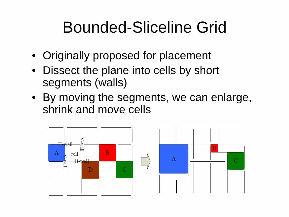
Bounded-Sliceline Grid• Originally proposed for placement• Dissect the plane into cells by short
segments (walls)• By moving the segments, we can enlarge,
shrink and move cells

Workflow of our router

Workflow of our router (cont’)

BSG embedding
• Can be done by heuristics like maze router• Need to follow some guidelines:
– Allow empty rooms between adjacent nets– Use proper number of BSG cells– Keep the topological relationships between
components and pins

BSG embedding

Key step: Cell sizing
• Need to size the cells so that the following constraints are satisfied:– Design rule– Component and pin location– Length(area) bounds for each net
• We formulate this problem as a mathematical programming problem

Experimental results
• Compare with Ozdal & Wong TCAD’06 LR-based router
• Tested on 7 data:– monotonic_1*, monotonic_2*, monotonic_3,
monotonic_4– general_1*, general_2, general_3
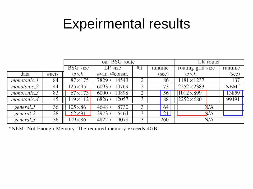
Expeirmental results

An example (general_3)

Escape RoutingT. Yan and M. Wong, DAC 2009

Escape Routing
․ Route (black) pins to the boundary of the pin grid array․ The grid has Orthogonal and Diagonal wiring capacity (O-cap and D-cap)

Traditional network-flow model
• O-cap can be guaranteed, but D-cap is not reflected• Some works assign node capacity to tile node, but it still
does not reflect D-cap correctly

When traditional model fails
• Assume O-cap = 2 and D-cap = 3• No constraints on tile node leads to illegal routing (a)• Let tile node capacity = 3 or less misses the legal routing
case (b)• Traditional network-flow model is not capable of
capturing diagonal capacity
O-cap
O-cap
O-cap
O-cap(b)(a)

Our Network Flow Model
W
S
N
EC : capacity = O-cap
: capacity = O-cap/2
: capacity = 1
: capacity = ∞
: node capacity = D-cap − 2⋅ O-cap/2
Node capacity implementation
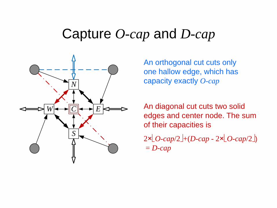
Capture O-cap and D-cap
W
S
N
EC
An orthogonal cut cuts only one hallow edge, which has capacity exactly O-cap
An diagonal cut cuts two solid edges and center node. The sum of their capacities is
2×O-cap/2+(D-cap - 2×O-cap/2)= D-cap

The Entire Flow Network
Pin Grid
(O=2, D=3)
Network
Optimal single-layer escape routing!
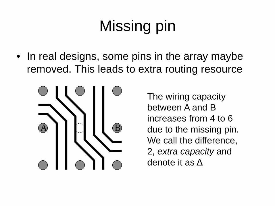
Missing pin
• In real designs, some pins in the array maybe removed. This leads to extra routing resource
A B
The wiring capacity between A and B increases from 4 to 6 due to the missing pin. We call the difference, 2, extra capacity and denote it as Δ

Consider missing pins in our model
Δ
11
∞1
11
1∞
1∞
11
∞1
11
• Consider the missing pin as a resource node
• The capacity of the resource node is exactly the extra capacity

Experimental results
• Tested on industrial data• Results indicate that our model has zero D-cap violation
for all data while traditional model has violations• Though our model is more complicated, the runtime are
comparable

A sample result

Pin AssignmentH. Kong, T. Yan and M. Wong, ASP-DAC 2010

Pin Assignment for Buses
31
One routing layer
32
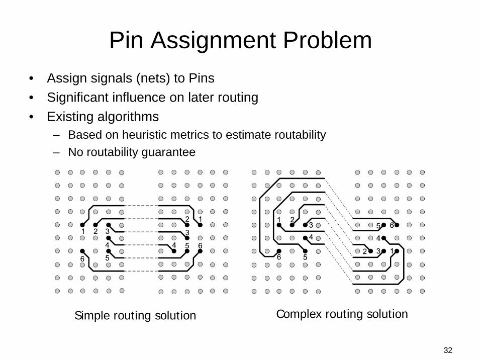
Pin Assignment Problem• Assign signals (nets) to Pins• Significant influence on later routing• Existing algorithms
– Based on heuristic metrics to estimate routability– No routability guarantee
Simple routing solution Complex routing solution
33
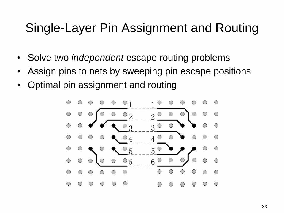
Single-Layer Pin Assignment and Routing
• Solve two independent escape routing problems• Assign pins to nets by sweeping pin escape positions• Optimal pin assignment and routing

Multi-Layer Pin Assignment and Routing
35
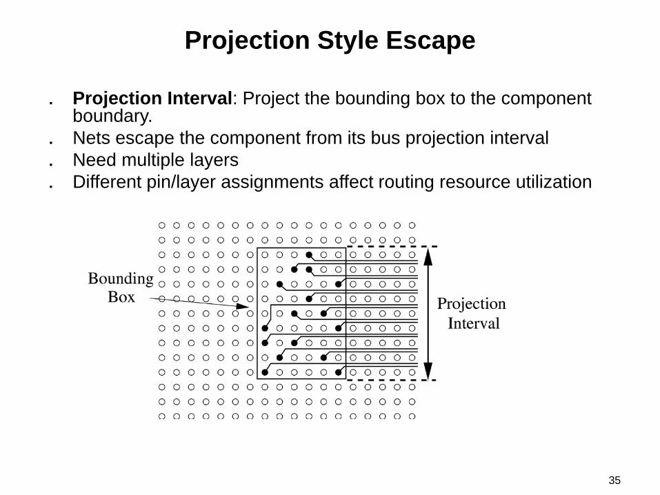
Projection Style Escape
․ Projection Interval: Project the bounding box to the component boundary.
․ Nets escape the component from its bus projection interval․ Need multiple layers․ Different pin/layer assignments affect routing resource utilization

36
Experimental Results․ Equal-length routing․ Back detours in the left component․ Complex length extension between component boundaries
Single-layer solution

37
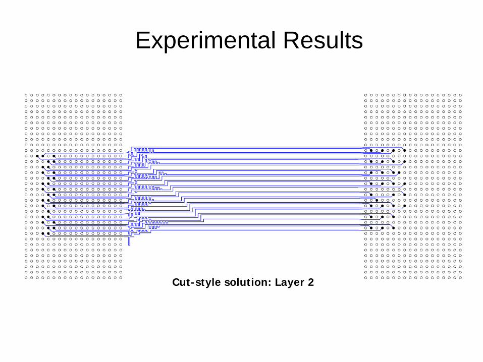
Experimental Results․ Equal-length solution․ No back detours․ Simple length extension between component boundaries
37.15% shorter total length 21.36% shorter escape wire length 44.96% shorter detailed wire length
Cut-style solution: Layer 1
Experimental Results
Cut-style solution: Layer 2

Experimental Results
• State-of-the-art industrial PCB– 7000+ nets– 80 buses– 12 routing layers– Previously routed manually
• manual routing typically takes 2 months per board
• Pin assignment and escape routing results– All 80 buses takes less than 5 minutes– The largest bus
• 338 nets• Takes 6 routing layers
39
Simultaneous EscapeLijuan Luo et al, ISPD-2010

Simultaneous Escape

Approach
• Net-by-net routing with various routing styles• Determine next net to route• Route net along routing boundary
Routing boundary

Experimental Results
• Performs significantly better than Cadence Allegro• Runtimes range from 0.2s to 289s

Experimental Results
Bus Escape ProblemHui Kong et al DAC 2010

46
Bus Escape Routing• Route nets from pins to component boundaries• Keep bus structures• Routing region for the bus is a boundary rectangle• Formulate as a Maximum Disjoint Subset problem.

47
Maximum Disjoint Subset (MDS) Problem• General rectangles NP-complete• Boundary rectangle Open Problem
– Rectangle attached to one or more boundaries
• We designed a polynomial time optimal algorithm!
Problem Solution