advanced hybrid solar cell approaches photovoltaic devices · meg or ib solar cell has a variety of...
TRANSCRIPT

Advanced Hybrid Solar Cell Approaches
for Future Generation Ultra-High Efficiency
Photovoltaic Devices
by
Jongwon Lee
A Dissertation Presented in Partial Fulfillment
of the Requirements for the Degree
Doctor of Philosophy
Approved April 2014 by the
Graduate Supervisory Committee:
Christiana Honsberg, Chair
Stuart Bowden
Ronald Roedel
Stephen Goodnick
Dieter Schroder
ARIZONA STATE UNIVERSITY
May 2014

i
ABSTRACT
Increasing the conversion efficiencies of photovoltaic (PV) cells beyond the single
junction theoretical limit is the driving force behind much of third generation solar cell
research. Over the last half century, the experimental conversion efficiency of both single
junction and tandem solar cells has plateaued as manufacturers and researchers have
optimized various materials and structures.
While existing materials and technologies have remarkably good conversion
efficiencies, they are approaching their own limits. For example, tandem solar cells are
currently well developed commercially but further improvements through increasing the
number of junctions struggle with various issues related to material interfacial defects.
Thus, there is a need for novel theoretical and experimental approaches leading to new
third generation cell structures.
Multiple exciton generation (MEG) and intermediate band (IB) solar cells have
been proposed as third generation alternatives and theoretical modeling suggests they can
surpass the detailed balance efficiency limits of single junction and tandem solar cells.
MEG or IB solar cell has a variety of advantages enabling the use of low bandgap materials.
Integrating MEG and IB with other cell types to make novel solar cells (such as MEG with
tandem, IB with tandem or MEG with IB) potentially offers improvements by employing
multi-physics effects in one device.
This hybrid solar cell should improve the properties of conventional solar cells with
a reduced number of junction, increased light-generated current and extended material
selections. These multi-physics effects in hybrid solar cells can be achieved through the
use of nanostructures taking advantage of the carrier confinement while using existing solar

ii
cell materials with excellent characteristics. This reduces the additional cost to develop
novel materials and structures.
In this dissertation, the author develops thermodynamic models for several novel
types of solar cells and uses these models to optimize and compare their properties to those
of existing PV cells. The results demonstrate multiple advantages from combining MEG
and IB technology with existing solar cell structures.

iii
DEDICATION
To beloved my parents and a little sister
And, to my committee member Dr. Dieter Schroder.
I am grateful for the encouragement and understanding as well as support from my
parents, sister and all of my friends. Especially, I am grateful to my parents and my sister,
Whanbok Lee (Father), Jungsook Kwon (Mother) and Soojin Lee (Sister) for their love,
encouragement, patience and sacrifice. I couldn’t have successively finished this long
journey without them.
Furthermore, Dr. Dieter Schroder was my admirable committee member until my
comprehensive examination. And, unfortunately, we have lost one of the greatest academic
honor two years ago.
His energetic and straightforward activities showed me the best example what a
professor should do in the university. His simple and clear directions gave me a manifest
way that I will follow as a way of researcher.
Even though I was regret to finish my journey with him, I want to say “extremely
thank you” to become my committee member for this dissertation.

iv
ACKNOWLEDGMENTS
First of all, I would like to express my sincere gratitude to my advisor, Dr.
Christiana B. Honsberg, for her support and guidance throughout my graduate studies at
Arizona State University. I greatly benefited from her deep intuition and strong knowledge
in the thermodynamic limit modeling for third generation photovoltaic devices and solar
cell design. I also want to thank my PhD committee members, Dr. Stuart Bowden, Dr.
Ronald Roedel and Dr. Stephen Goodnick, for agreeing to serve on my committee and for
their time spent on my committee. Also, special thanks to Dr. Dieter Schroder, for his
intuitive and great guidance and encouragement until my comprehensive examination. I
am really regretted that I could not finish my journey with him. It was wonderful moments
with him in Arizona State University.
I also would like to show my sincere gratitude to Dr. Kwangseok Seo in Seoul
National University and Dr. Weongook Jeong in Sung Kyun Kwan University as my
mentors and advisors. Without their deep and meaningful advices while I have struggled
in U.S, I could not finish my journey.
I would like to show my sincere gratitude to Dr. Jaechan Lee and Dr. Kangmin
Chung in Sung Kyun Kwan University who they have advised about study in US.
I would like to thank the graduate students and my friends who worked with me on
my research projects and enjoyed life at Arizona State University; namely, Korean Brothers
(Yeongho Kim (Hozzang), Jaewon Oh, Jaeyoung Choi, Sangpyung Kim, Jaewoong Chung,
Junghoon Lee, Keebeom Kim, Jaehee Park, Sungchan Lim, Hanjoe Kim) and Younghoon
Song who has been my best friend more than eight years in United States.

v
I also want to express my appreciation to all my colleagues in the Arizona State
University Solar Power Laboratory for helpful conversations regarding research; especially
to Mr. Bill Dauksher, Dr. Nikolai Faleev and Dr. Clarence Tracy. Furthermore, special
thanks goes to the secretary of QESST, Michele Nobles, Regina Sanborn and Rebecca
Davis for her kind help.

vi
TABLE OF CONTENTS
Page
LIST OF TABLES .................................................................................................................... x
LIST OF FIGURES .............................................................................................................. xiii
CHAPTER
1 INTRODUCTION ........................................................................................................ 1
1.1 Solar Energy ............................................................................................... 1
1.2 The Current Issues for Solar Cells for Future Generation PV .................. 5
1.3 Thermodynamic Approaches for Nanostructured Solar Cells.................. 8
1.4 Motivation for Hybrid Approaches ........................................................... 9
1.5 Dissertation Outline ................................................................................. 11
2 Thermodynamic Limits of Single junction, tandem, Multiple exciton generation,
Intermediate Band solar Cells .................................................................................... 15
2.1 Background of Detailed Balance Limits ................................................. 15
2.2 The Detailed Balance Limit .................................................................... 18
2.3 Tandem Solar Cells .................................................................................. 22
2.4 The Multiple Exciton Generation Solar Cells ......................................... 26
2.5 The Intermediate Band Solar Cells ......................................................... 29
3 IMPACT OF THRESHOLD ENERGY ON LIMITING EFFICIENCIES IN
MULTIPLE EXCITON GENERATION SOLAR CELLS ...................................... 33
3.1 Introduction .............................................................................................. 33
3.2 Theory .................................................................................................... 36
3.3 Results .................................................................................................... 39

vii
CHAPTER Page
3.4 Conclusion................................................................................................ 44
4 Limiting Efficiencies of Multijunction Solar Cells with Multiple Exciton Generations
... ................................................................................................................................. 45
4.1 Introduction .............................................................................................. 45
4.2 Multijunction Solar Cells with MEG Process ......................................... 45
4.3 Theory .................................................................................................... 47
4.3.1 Detailed Balance Calculations Including MJMEG .............. 47
4.3.2 Spectral Splitting in MJMEG Solar Cells ............................ 52
4.4 Results .................................................................................................... 53
4.4.1 Impact on Optimum Bandgaps ............................................ 57
4.4.2 Impact on Sensitivity of Efficiency to Bandgap .................. 59
4.4.3 The Discussion of 2J and 3J MJMEG Devices under 900 Suns
.............................................................................................. 61
4.5 Conclusion................................................................................................ 62
5 Limiting Efficiency of Silicon Based Nanostructure Solar Cells for Third Generation
Solar Cells ................................................................................................................... 64
5.1 Introduction .............................................................................................. 64
5.2 Theory .................................................................................................... 65
5.2.1 The Importance of Silicon Materials ................................... 65
5.2.2 The effective bandgap of silicon nanostructure ................... 66
5.2.3 Silicon MEG ........................................................................ 67

viii
CHAPTER Page
5.2.4 MJMEG Solar Cells with silicon QDs ................................. 70
5.3 Results and discussion ............................................................................. 71
5.3.1 Silicon MEG solar cell ......................................................... 71
5.3.2 MJMEG hybrid solar cells with Si QDs .............................. 75
5.4 Conclusion................................................................................................ 78
6 THE EXPERIMENTS OF SILICON NANOSTRUCTURE SOLAR CELLS ....... 79
6.1 Introduction .............................................................................................. 79
6.2 Silicon Nanostructured Solar Cells ......................................................... 81
6.3 Experimental Procedure ........................................................................... 82
6.4 Results .................................................................................................... 86
6.4.1 The Electrical Characteristics .............................................. 86
6.4.2 The Optical Characteristics .................................................. 89
6.5 Conclusion................................................................................................ 90
7 Limiting Efficiencies of Intermediate Band Solar Cells with Tandem Configuration
..................................................................................................................................... 92
7.1 Introduction .............................................................................................. 92
7.2 Theory .................................................................................................... 94
7.2.1 Detailed Balance Model of IBTSC ...................................... 94
7.2.2 Solar Spectrum Splitting of Double Junction IBTSC .......... 97
7.3 Results .................................................................................................... 99
7.3.1 The thermodynamic Limits of double junction IBTSCs...... 99

ix
CHAPTER Page
7.3.2 Material Selection for IBTSC ............................................ 103
7.4 Conclusion.............................................................................................. 104
8 THE THERMODYNAMIC LIMIT OF INTERMEDIATE BAND SOLAR CELLS
ASSISTED WITH MULTIPLE EXCITON GENERATION ................................ 105
8.1 Introduction ............................................................................................ 105
8.2 Theory .................................................................................................. 107
8.2.1 Detailed Balance of MIBSC .............................................. 107
8.2.2 Carrier Transitions of MIBSC ........................................... 109
8.2.3 The Possibility of Carrier Multiplication in MIBSC ......... 112
8.3 Results .................................................................................................. 113
8.4 Conclusion.............................................................................................. 116
CHAPTER 9 Conclusion ...................................................................................................... 118
REFERENCES ..................................................................................................................... 122
APPENDIX
A COPYRIGHT OF CHAPTER 1 ................................................................................. 136
B COPYRIGHT OF IEEE IN CHAPTER 2, 4, 5.......................................................... 138
C THE QUANTUM YIELD OF MJMEG SOLAR CELL ........................................... 140
D COPYRIGHT OF CHAPTER 6 ................................................................................ 144
E COPYRIGHT OF SPIE IN CHAPTER 7 .................................................................. 146
x
LIST OF TABLES
Table Page
2.1 The maximum efficiency and optimum bandgap of single junction solar cell with
different spectrum and concentration. .............................................................. 21
2.2 The relationship of theoretical efficiencies for tandem solar cells between an
independent connection and a series-connection. J is the current density and V
is the operating voltage, Jm is the current density at maximum power point and
Vm is the operating voltage at maximum power point. Pmax is the maximum
power, and i=1,2,3…N.. ................................................................................... 24
2.3 The efficiency table of double junction tandem solar cells under one sun
illumination with terrestrial spectrum (AM1.5G spectrum). ............................ 26
2.4 The optimum bandgaps and maximum efficiency of full concentration for a
single IBSC with blackbody radiation. ............................................................. 32
2.5 The optimum bandgaps and maximum efficiency of conventional triple junction
solar cells for independent and series connection under full concentration with
blackbody radiation. ......................................................................................... 32
3.1 Efficiency vs optimum Eg (eV) for ideal QY and Non-Ideal QY for Blackbody
Radiation and ASTMG 173-03 where η (%) is the maximum conversion
efficiency, M is the maximum ideal quantum yield and Eth is the threshold
energy. .............................................................................................................. 42
4.1 Independent connection for MJ and MJMEG (BB and AM1.5G, One sun) where
BB is the blackbody radiation and AM is the terrestrial spectrum, η is the
maximum conversion efficiency © [2014 IEEE] [69]. .................................... 54

xi
Table Page
4.2 Series Connection for MJ and MJMEG (BB and AM1.5G, One sun), © [2014
IEEE] [69] ........................................................................................................ 55
4.3 Independent Connection for MJ and MJMEG (BB and AM1.5D, C=46200), ©
[2014 IEEE] [69] .............................................................................................. 55
4.4 Series Connection for MJ and MJMEG (BB and AM1.5D, C=46200), © [2014
IEEE] [69] ........................................................................................................ 56
5.1 The effective Si QD bandgap vs diameter © [2013 IEEE] [94]. ...................... 67
5.2 The efficiency of Si MEG ideal QY and non-ideal QY under one sun (ASTMG
173-03) © [2013 IEEE] [94]. ........................................................................... 72
5.3 The efficiency of Si MEG with ideal QY and non-ideal QY with changing
concentration where C is concentration. (Effective Eg=1.2 eV) ...................... 74
5.4. The double junction of MJMEG solar cells using Si QDs for upper junction
where S is the series connection. H stands for MJMEG Hybrid solar cells. IQY
is the ideal QY and NQY is the non-ideal QY. ................................................ 76
6.1 The electrical characterization results of silicon-nanostructured solar cells
[Christopher Green, NNIN REU, 2013] [62] ................................................... 86
7.1 The optimum bandgaps and maximum efficiency (η) of independent (I) and
series (S) connected double junction IBTSCs under blackbody radiation with full
concentration [J.Lee, [111],2012]. ................................................................. 100
7.2 The optimum bandgaps and maximum efficiency (η) of six junction tandem solar
cell under blackbody radiation where concentration (=Conc) is 46200 sun [J.Lee,
[111],2012] ..................................................................................................... 101

xii
Table Page
8.1 The comparison of both conversion efficiencies and optimum bandgaps between
IBSC and MIBSC under blackbody radiation with one sun and full concentration
where N is the number of electrons and η is the maximum conversion efficiency.
........................................................................................................................ 113
8.2 The comparison of both conversion efficiencies and optimum bandgaps between
IBSC and MIBSC under terrestrial spectrum with one sun and full concentration.
........................................................................................................................ 114

xiii
LIST OF FIGURES
Figure Page
1.1 World energy consumption, 1990-2040, [U.S. Energy Information
Administration ,July 2013] [1] (see Appendix. A) ............................................. 2
1.2 Efficiency vs cost of 1st, 2nd, and 3rd generation solar cells[4]. .......................... 4
1.3 Solar cell efficiency chart from 1975 to 2013 [National Renewable Energy
Laboratory (NREL), Golden, CO., 2013] [5] ..................................................... 5
1.4 The operation of a solar cell [7] ......................................................................... 6
1.5. The proposed hybrid solar cells: (a) The properties of solar cells (b) Hybrid
Approaches and (c) is the advantages of hybrid solar cells. ........................... 10
1.6 The development of hybrid concepts of solar cells using detailed balanceshows:
(a) MEG and multijunction-tandem hybrid solar cells, (b) the intermediate band
and tandem hybrid solar cells and (c) MEG+IB hybrid solar cells. ................. 12
2.1 (a) In this solar cell model (a), the detailed balance limit, shows T1 representing
solar radiation as it relates to the temperature of the sun with full exposure. Fig.
2.1b (T2) also shows temperature radiation angles within the solar cell, but this
model is only partially exposed to the sun [7]. ................................................. 16
2.2 Illustration of solar photon energy distribution between the Sun and the Earth. .
.......................................................................................................................... 17
2.3 This illustration shows the process of one-electron and hole pair generation of a
single junction solar cell where µ is the chemical potential, and εFC and εFV are
the Fermi level at conduction band and valence band, respectively. ............... 19

xiv
Figure Page
2.4 The efficiency with Eg variation of single junction solar cells (Black Body and
terrestrial spectrum) where (a) is blackbody radiation with one sun and full
concentration (C=46200) and (b) is terrestrial spectrum with one sun and for full
concentration (C=46200) .................................................................................. 21
2.5 The schematic of tandem solar cells: (a) shows is the general schematic of
tandem solar cells, (b) shows a two-junction independent connection, and (c)
shows a two-junction series connection where Eg(i) stands for bandgap energy of
each sub-cell in tandem solar cells, and i=positive integer. ............................ 24
2.6 The spectral splitting of double junction tandem solar cells ............................ 25
2.7 The efficiency contour of 2 junction tandem solar cells .................................. 26
2.8 (a) Thermalization of electrons of single junction solar cells results in energy
loss and heat generation; (b)MEG has the potential to create more than one EHP
per absorbed high energy photon where Eph is the photon energy, CB is the
conduction band, VB is the valence band and I.I is the impact ionization © [2013
IEEE] [22]. (see Appendix. B). ....................................................................... 27
2.9 The carrier transitions of intermediate band solar cells, where Eg is the bandgap,
ECI is energy between intermediate band and conduction band, EIV is the energy
between intermediate band and valence band, subscripts (V, I, C) are valence
band, intermediate band and conduction band respectively. ............................ 30
2.10 Efficiency vs bandgap of conventional intermediate band solar cells under fully
concentrated sunlight (C=46200) accounting for bandgap optimization. ........ 31

xv
Figure Page
3.1. (a) Thermalization of electrons of single junction solar cells results in energy
loss and heat generation; (b) Multiple Exciton Generation results in more than
one EHP per absorbed high energy photon where Eph is the photon energy, Eg is
the bandgap energy, CB is the conduction band, VB is the valence band. ...... 35
3.2. (a) Ideal QY for three different bandgaps under the AM1.5 spectrum and (b)
non-ideal QY with A=1 for one value of Eg (=1.12eV) and three different
threshold energies. ............................................................................................ 37
3.3. Efficiency vs Eg with ideal QY for one sun and maximum concentration for
Blackbody Radiation and terrestrial spectrum where M is the maximum
QY................................................................................................................................40
3.4. Efficiency vs Eg for non-ideal QY as a function of threshold energy under both
one sun and full concentration (Blackbody radiation and terrestrial
spectrum).....................................................................................................................41
4.1. Spectral splitting and QY in conventional MJ and MJMEG solar cells. (a) A four
junction MJ solar cell. The QY of each region is 1. (b) Ideal QY for a
multijunction device with MEG © [2014 IEEE] [69]. ..................................... 48
4.2. Efficiency contour for a 2J MJ and MJMEG hybrid at one sun, BB spectrum
independently connected © [2014 IEEE] [69]. ................................................ 58
4.3 Efficiency contour for a 2J MJ and MJMEG hybrid at one sun, BB spectrum
series connected, © [2014 IEEE] [69]. ............................................................. 58
4.4 Efficiency contour for a 2J MJ and MJMEG at maximum concentration, BB
spectrum series connected, © [2014 IEEE] [69]. ............................................. 58

xvi
Figure Page
4.5 Simulated efficiency contour for a 2J MJ and MJMEG hybrid at one sun,
AM1.5G spectrum, series connected, © [2014 IEEE] [69]. ............................. 59
4.6 Simulated efficiency contour for a 2J MJ and MJMEG hybrid at maximum
concentration, AM1.5D spectrum, series connected, © [2014 IEEE] [69]. ..... 59
4.7 Simulated efficiencies of series-connected 2J(=(a),(b)) and 3J(=(c), (d))MJ and
MJMEG solar cells under 900 suns. Eg1 and Eg2, Eg2 and Eg3 and Eg3 and Eg1
planes are used to plot in Fig.7 (c) and (d) © [2014 IEEE] [69]. ..................... 61
5.1 The effective bandgap as a function of diameter for Si QDs © [2013 IEEE] [94].
.......................................................................................................................... 67
5.2 The QY and photon energy of silicon QD, The maximum value of ideal QY is 3
and changes the delayed Eth as 2Eg, 3Eg and 4Eg. (a) Eg=1.12eV, (b) Eg=1.2 eV,
(c)Eg=1.3 eV and (d)Eg=1.4 eV © [2013 IEEE] [94]. ...................................... 69
5.3 The spectral splitting of double junction-MJMEG solar cells. The maximum QY
depends on its bandgaps of each junction (a) and (b) are under one sun
illumination, (c) and (d) are under full concentration (C=46200) © [2013 IEEE]
[86] for Fig. 6.3 (a) and (c). . ............................................................................ 71
5.4 The Efficiency VS Concentration of Si (Eg=1.2 eV) MEG under terrestrial
spectrum with concentration. The concentration axis presents as log scale
where M is the maximum QY © [2013 IEEE] [94]. ........................................ 74
6.1 The experiment flows of silicon nanostructured solar cells ............................. 83
xvii
Figure Page
6.2 The fabrication of silicon nanostructures where (a) is the SEM image for
deposition of 30nm thickness SiO2 (b) is the image for silicon nanostructures
after deep RIE etching [Christopher Green, NNIN REU, 2013] [62]. ............. 85
6.3 The electrical properties of silicon nanostructured solar cell [Christopher Green,
NNIN REU, 2013] [62]. ................................................................................... 87
6.4 The cross-section and top-view of silicon nanostructured solar cells .............. 89
6.5 The measurements of reflectance between silicon nanostructures PV cell and
textured Si PV and Bulk or bare silicon solar cells [Christopher Green, NNIN
REU, 2013] [62]. .............................................................................................. 90
7.1 The schematic of a tandem double junction IBTSC. ........................................ 95
7.2. The schematic of electrical circuit model of IBSC. It is composed of three diodes
having bandgaps of ECI, EIV and ECV ............................................................... 95
7.3 The spectral splitting of two regions for 2J IBTSC .......................................... 98
7.4 Efficiency vs. Ehi(1) for double junction with an independent connection (red line)
and a series-connection (blue line) under full concentration (J.Lee, [111],2012).
........................................................................................................................ 100
7.5 Two types of band structures for a double junction IBTSC where (a) is type I
and (b) is the type II. ...................................................................................... 102
8.1 The QY of three transitions in the MIBSC, (a) Without restrictions for carrier
multiplication, the order of bandgaps is ECI<2ECI < EIV<2EIV <Eg(=ECV) < 2Eg .
(b) The modified carrier generations of MIBSC. ECI<2ECI < EIV<Eg(=ECV)< 2EIV .
........................................................................................................................ 110
xviii
Figure Page
8.2 The procedure of generation of carriers in the MIBSC, Eph is the photon energy.
(a) The number of electrons=2. (b) The number of electrons=3 which 2 is from
VB to CB and 1 is IB to CB, (c) The number of electrons=3 which 1 is from VB
to CB and 2 is IB to CB and (d) The number of electrons=4. The 4 EHPs are
generated that 2 is from VB to CB and 2 is from IB to CB ........................... 111
8.3 The efficiencies vs optimum Eg where (a) is the one sun illumination (C=1) and
(b) is the maximum concentration (C=46200) under blackbody radiation. ... 113
8.4 The efficiencies vs optimum Eg where (a) is the one sun illumination (C=1) and
(b) is the maximum concentration (C=46200) under terrestrial spectrum. .... 114
8.5 The three bandgap alignments at the maximum conversion efficiency. (a) The
total number of generated electrons is 3 under blackbody radiation. The optimum
bandgaps under blackbody radiations are ECI=0.47 eV, EIV=0.93 eV and Eg=1.40
eV. (b) The total number of generated electrons is 3 under terrestrial spectrum.
The optimum bandgaps under terrestrial spectrum are ECI=0.51 eV, EIV=1.00 eV
and Eg=1.51 eV............................................................................................... 116

1
CHAPTER 1
INTRODUCTION
1.1 Solar Energy
The development of energy technologies is important to modernized societies with
benefits that will improve quality of life for generations to come. After the mid-20th
century, electric or power was considered a major gift to civilization. Until the early 21st
century, fossil fuel and nuclear technologies were the leading energy sources to provide
benefits to world. However, fossil fuels and nuclear power have major issues due to both a
dwindling work force and leak potential for nuclear plants (magnified by the 2011
Fukushima Daiichi disaster) as well as a limited coal supply due to be depleted within the
next 200 years plus the environmental contamination of carbon dioxide emissions and ash
disposal practices of coal-fired power plants. Currently, solar energy is the most promising
future generation energy resource because of it is clean and permanent. However, existing
energy resources are still the dominant providers of electricity for both industrial and
commercial purposes. Furthermore, energy consumption has been extensively increased
due to the demands of diverse fields, which are deeply related to the industrial and
economic status of countries worldwide. Thus, the implementation of nuclear energy has
tremendously increased in that past 50 years. Practically, the energy consumption is
expected to increase by 56% between 2010 and 2040. Fig. 1.1 shows world energy
consumption going from 524 quadrillion British thermal units (Btu) in 2010 to 630
quadrillion Btu in 2030 and to 820 quadrillion Btu in 2040 [1]. Energy consumption from
Non-Organization for Economic Co-operation and Development (OECD) nations is

2
expected to dramatically increase after 2020 compared to OECD countries. Non-OECD
countries are still developing their infrastructures and enhancing their novel technologies
based on investments from the global companies in OECD countries. Thus, it may require
more time and money to develop their countries.
Fig.1.1. World energy consumption, 1990-2040, [U.S. Energy Information
Administration ,July 2013] [1] (see Appendix. A)
In other words, even though energy consumption will increase more than 50% in
the future, it is still dependent on the oil and nuclear power to maintain their facilities [1].
Due to limited usages and environmental contamination from both coal and nuclear plants,
utilization of these sources should decrease as in favor of renewable alternatives.
According to the “Annual Energy Outlook 2013 with Projections to 2040,” Executive
Summary: “Electricity generation from solar and, to a lesser extent, wind energy sources
grows as their costs decline, making them more economical in the later years of the
projection.” [U.S. Energy Information Administration, July 2013] [2].

3
Even if the future of solar energy is bright, the lack of solar energy infrastructure
and cost of installation hinders development. Even though the solar cell is popular energy
resource, electricity suppliers are still focused on providing solar cells based on income
analysis and regional differences. In other words, solar energy use is still restricted for the
most part to individuals who can afford solar cells.
Therefore, to satisfy rapidly increasing demands for green energy and to relieve the
problems of economic status, an urgent need exists to increase the efficiency and reduce
the cost of electricity (COE) in $/kWh [3],[4]. But, solar energy still shows relatively high
COE compared to the existing energy sources so that increasing the conversion efficiency
is a key to reducing COE of photovoltaic (PV) devices. Furthermore, the national energy
policies should also support an increase in the general use of solar energy.
Even though researchers are focused on increasing the conversion efficiency of PV
devices by investigating semiconductor materials from periodic table of the element such
as silicon, group III-V and group II-V, existing methods like thin-film solar cells or tandem
solar cells are going to meet limitations due to their own material properties.
For instance, the II-VI material-based thin film solar cell shows about 10% range
of conversion efficiency due to organic material properties. Tandem solar cells present the
greatest improvement of solar cell efficiency, but their material properties are problematic
due to the need for increasing the number of carriers.
To overcome these issues, new or innovative concepts are still needed to enhance
PV conversion efficiency by both theoretical and experimental approaches. In Fig. 1.2, the
wafer and thin film based first and second generation solar cells display high cost and low
conversion efficiency [4]. But, third generation solar cells like tandem, multiple exciton

4
generation, hot carrier, and intermediate band solar cells can reduce cost and increase
efficiency (see Fig. 1.2) [4].
Fig 1.2. Efficiency vs cost of 1st, 2nd, and 3rd generation solar cells [4].
In Fig. 1.3, the current efficiency records of solar cells have dramatically increased
to the point that tandem solar cells are leading PV devices with concentrators to achieve
50% conversion efficiency [5],[6]. Further, the single junction silicon PV, Heterojunction
with Intrinsic Thin-layer and GaAs-based III-V solar cell are also approaching 30%
conversion efficiency [5],[6].
In Fig. 1.2, 30% of single junction solar cells’ efficiencies are the range of first and
second generation PV devices, which show high COE. Even if the efficiency of tandem
solar cells display the range of third generation PV devices, it has to increase the number
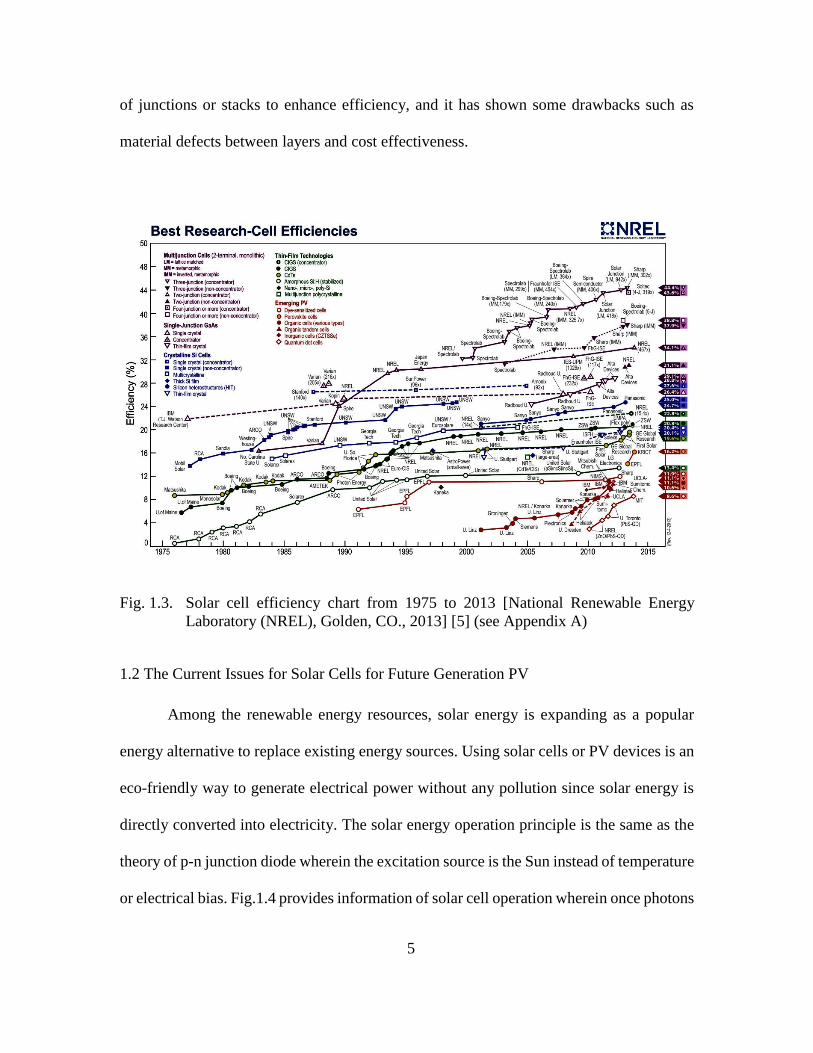
5
of junctions or stacks to enhance efficiency, and it has shown some drawbacks such as
material defects between layers and cost effectiveness.
Fig. 1.3. Solar cell efficiency chart from 1975 to 2013 [National Renewable Energy
Laboratory (NREL), Golden, CO., 2013] [5] (see Appendix A)
1.2 The Current Issues for Solar Cells for Future Generation PV
Among the renewable energy resources, solar energy is expanding as a popular
energy alternative to replace existing energy sources. Using solar cells or PV devices is an
eco-friendly way to generate electrical power without any pollution since solar energy is
directly converted into electricity. The solar energy operation principle is the same as the
theory of p-n junction diode wherein the excitation source is the Sun instead of temperature
or electrical bias. Fig.1.4 provides information of solar cell operation wherein once photons
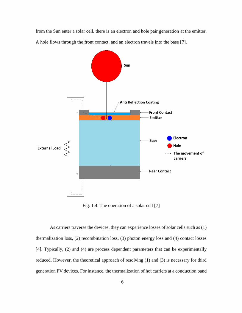
6
from the Sun enter a solar cell, there is an electron and hole pair generation at the emitter.
A hole flows through the front contact, and an electron travels into the base [7].
Fig. 1.4. The operation of a solar cell [7]
As carriers traverse the devices, they can experience losses of solar cells such as (1)
thermalization loss, (2) recombination loss, (3) photon energy loss and (4) contact losses
[4]. Typically, (2) and (4) are process dependent parameters that can be experimentally
reduced. However, the theoretical approach of resolving (1) and (3) is necessary for third
generation PV devices. For instance, the thermalization of hot carriers at a conduction band

7
is the dominant loss in the PV devices that can be reduced by multiple EHPs of single
junction solar cells. Furthermore, (3) can be managed by splitting solar spectrum through
tandem and intermediate band solar cells.
The recent records of solar cells in Fig 1.3 have indicated that the existing
technologies will approach its material induced limit. For example, the recent world
records for using the most single junction solar cells indicate that UNSW reported using
about 25% Si solar cells and Alta Devices claimed using 28.2% AlGaAs/GaAs cascade
materials [5],[6],[8],[9]. And, the current report of thin-film amorphous silicon solar cells
has indicated 25.6%. [10]. These records have approached to the ideal single junction limit
as 31%.
Tandem solar cells are well-commercialized PV devices due to high conversion
efficiency with light-concentrators. Current world records of tandem solar cells have been
presented at 3J and 4J junction tandem solar cells. In a triple junction tandem solar cells,
InGaAs (=1.00 eV)/GaAs (=1.42 eV)/InGaP (=1.89 eV) inverted metamorphic growth
show 44.4% at 302 suns [6]. It is also shown 44.7% of four junction tandem solar cells
from Fraunhofer ISE, Soitec, CEA-Leti and Helmholtz Center Berlin. This approach is
composed of a wafer bonding structure with two dual junctions which its material
composition is (InGaP(1.89 eV)/ GaAs (1.42 eV)// InGaAsP (1.05 eV) / InGaAs (0.73eV),
297 Suns) [11]. But, its theoretical efficiencies from the detailed balance limit indicate 54.8%
of 3J, and 59.4% of 4J from the same configurations. There is also more than 10%
difference between theoretical and experimental efficiencies so that it is still necessary
further developments to improve the entire properties of tandem solar cells.

8
The clear ways to enhance tandem solar cells are increasing the number of junctions
and develop its corresponding materials. But, the current methods can face to approach to
the theoretical limit of tandem solar cells due to defect issues.
1.3 Thermodynamic Approaches for Nanostructured Solar Cells
The thermodynamics limit or detailed balance limit of solar cells are the general
test bed for developing new concepts for PV cells. Since Shockley and Queisser (SQ)
developed the detailed balance of single junction in 1961 [12], it has been strong tools to
expect the theoretical limit of proposed solar cells.
In section 1.2, the author discusses the large difference between theoretical limit
and experimental results of solar cells because of excluding non-radiative recombination
in the detailed balance limits. Further, solar cells have their own material induced limits,
for instance, silicon is an indirect bandgap materials in which there is an indirect transition.
To suppress these properties, making nanostructured solar cells is a good candidate because
of excellent quantum confinement and relaxed momentum conservation. And,
nanostructured solar cells have a good light-control for better absorption.
There are many proposed types of third generation PV cells such as multiple exciton
generation (MEG) solar cells from many electron and hole pairs per one incoming photon,
intermediate band solar cell (IBSC) by three carrier transitions and hot carrier solar cells.
In the 1990s, various concepts such as multiple exciton generation (MEG) and
intermediate band solar cells (IBSC) were proposed and their limiting efficiencies were
also calculated to surpass the SQ limits.

9
MEG is a carrier multiplication solar cell per an incoming photon by impact
ionization. Werner reported the limiting efficiencies of multiple exciton generation that its
theoretical limit under one sun is about 45%after finding 130% of quantum efficiency in
silicon and its optimum bandgaps are lowered about 0.7 eV [13], [14]. Luque and Marti
proposed IBSC in 1997 and its theoretical limit is about 63% that it is similar to triple
junction tandem solar cells, and active research using quantum dots of III-V materials is
still being conducted in many groups with current reports about efficiencies around 20%
[15],[16]. Tandem solar cells are the well-known commercialized PV cells with stacked
different bandgap materials, and current reports shows over 40% utilization with
concentrators [5],[6].
1.4 Motivation for Hybrid Approaches
Theoretical approaches for nanostructured solar cells have provided great impact
to developing novel types of solar cells to achieve more than 50% conversion efficiency
for future generations solar cells.
As described in previous sections, continual improvements in efficiency are
necessary to achieve approaches in which the levelized electricity cost is low.
Nanostructured approaches and advanced concept approaches have been long suggested as
a means of realizing efficiencies above the SQ limit. However, nanostructures and
advanced concept approaches have not achieved an improvement in efficiency, due to a
combination of the fundamental concepts themselves, as well as the materials suggested
for their implementation. For example, the conventional intermediate band approach has a
lower theoretical efficiency that a four junction tandem, which has already been

10
experimentally realized. Similarly, MEG approaches often utilize low band gaps and
materials which have not a commercial or high efficiency experimental base. Moreover,
MEG approaches, unless they use unrealistic concentration levels, and highly idealized
assumptions, also have theoretical efficiencies below approaches already implemented.
Thus, the overarching motivation of the thesis is to overcome these limits, primarily by
developing hybrid approaches, which allow known materials to approach thermodynamic
limits. In addition, for the special case of silicon, the thesis shows that the inclusion of
MEG processes can realize high efficiencies.
Fig.1.5. The proposed hybrid solar cells: (a) The properties of solar cells (b) Hybrid
Approaches and (c) is the advantages of hybrid solar cells.

11
For instance, (1) combining with MEG with multijunction solar cells offers the
improved conversion efficiency with low bandgap material choices, (2) integrating IBSC
with tandem solar cells provides the increased theoretical conversion efficiency with
reduced number of junctions and (3) carrier multiplication effect in IBSC give an advantage
of material choices at low bandgap region with improved theoretical efficiency.
It is summarized in Fig 1.5 that describes (1) the properties of MEG, IBSC and
tandem solar cells, (2) the combination procedures of existing technologies with 3rd
generations PV of nanostructures and (3) the advantages of three proposed hybrid solar
cells.
Moreover, other benefits of hybrid solar cells in thermodynamics have provided the
wide selections of materials. For example, because of MEG effect of each junctions in
tandem solar cells or intermediate band solar cells, the overall optimum bandgaps have
reduced while comparing the existing optimum materials. And, intermediate band and
tandem hybrid approaches make it possible to choose from group IV, III-V and II-V
combinations.
1.5 Dissertation Outline
In this dissertation, the author proposes the hybrid concept solar cell with a
combination of third generation photovoltaic cell theory to search the multi-points of
benefits. The general sequence of each proposed concept is calculated by combining its
detailed balance theory and investigating appropriate materials.
In Fig.1.6, process flows are presented to introduce the hybrid solar cells. The first
two models are the detailed balance limit of tandem solar cells with multiple exciton

12
generation solar cell (see Fig.1.6 (a)) and intermediate band solar cells (see Fig.1.6 (b)) to
improve the characteristics of tandem or multijunction solar cells. And, the last model is
the thermodynamic model of carrier multiplications of intermediate band solar cell (see
Fig.1.6 (c)).
Fig. 1.6. The development of hybrid concepts of solar cells using detailed balanceshows:
(a) MEG and multijunction-tandem hybrid solar cells, (b) the intermediate band
and tandem hybrid solar cells and (c) MEG+IB hybrid solar cells.
The introduction explains the needs in solar cell technology and the purpose of this
research along with its motivation. Chapter 2 introduces the detailed balance limit of single
junction solar cell, MEG, tandem and intermediate band solar cells to understand and
support the novel concept of hybrid solar cells. In chapter 3, the author discusses the
thermodynamic limit of MEG solar cells and how low optimum bandgap materials can
benefit the multijunction solar cell, and the delayed threshold energy can provide the
impact of reducing MEG effect through different light concentration.
In chapter 4, the author will discuss MEG and multijunction hybrid solar cells with
assumption of carrier multiplications at each junction where a small number of junctions
is achieved with enhanced theoretical conversion efficiencies compared to conventional

13
tandem solar cells. For instance, two or three junctions of MEG and multijunction hybrid
solar cells are shown as having better performance than three or four junctions of tandem
solar cells.
In chapter 5, based on the theory behind the interaction of MEG and multijunction
hybrid solar cells, the author discusses limiting efficiencies of silicon-based MEG solar
cells with a concentrator and various threshold energies. Further, silicon-based double
junction MEG and multijunction hybrid solar cells are discussed where silicon (with 1.12
eV bandgap) is used at the upper junction materials and the appropriate bottom junction
materials are searched based on theoretical efficiency calculations. Chapter 5 also includes
the non-ideal quantum yield to calculate the limiting efficiency of silicon-based
nanostructured multijunction solar cells.
In chapter 6, experimental results are discussed of electrical and optical properties
of a proto-type silicon nanostructured solar cell that that it is defined by electron beam
lithography and reactive ion etching technology. The author discusses the importance of
silicon nanostructured solar cells for further improvements like carrier multiplications. Its
experimental conversion efficiency achieved about 6.4% conversion efficiency including
an increased light-generated current, which has an optical resonance near bandgap of
amorphous-silicon region.
Chapter 7 will discuss the detailed balance limit of intermediate band and tandem
solar cells showing how a double junction in this hybrid solar cell can gain efficiency
comparable to the conventional six-junction tandem solar cells. This efficiency gain is due
to three carrier transitions in the intermediate band solar cells. After calculating the detailed

14
balance limit, the author discusses the appropriate material needed for above 3eV
intermediate band and tandem hybrid solar cells.
Chapter 8 covers intermediate band solar cells of carrier multiplications hybrid
solar cells. The intermediate band (IB) has metallic properties which are at half-filling
states. The properties of IB for MEG in IB solar cells will be discussed through carrier
multiplication of IBSC.
Finally, the author will offer conclusions presenting the overall benefits of hybrid
solar cells and discuss future research.

15
CHAPTER 2
THERMODYNAMIC LIMITS OF SINGLE JUNCTION, TANDEM, MULTIPLE
EXCITON GENERATION, INTERMEDIATE BAND SOLAR CELLS
2.1 Background of Detailed Balance Limits
The detailed balance limit is the theoretical approach most typically used to
calculate the performance limits for solar cells. It is the primary tool used in this research
to calculate the efficiency of the proposed PV approaches. The following chapter presents
the detailed balance approach, and applies it to the advanced concepts of multiple exciton
generation and intermediate band processes.
. Detailed balance was applied to solar cells by William Shockley and Hans J.
Queisser, who showed that a single p-n junction solar cell has a theoretical efficiency limit,
also known as the Shockley-Queisser limit or the detailed balance limit [8].
The detailed balance limit is deeply related to thermodynamics, which is based on
four fundamental laws:
(1) The zeroth law states that when two systems sit in equilibrium with a third
system, they are also in thermal equilibrium with each other;
(2) The first law, also known as Law of Conservation of Energy, states that
energy cannot be created or destroyed; it can, however, be redistributed or
changed from one form to another.
(3) The second law refers to the increased entropy that occurs in any isolated
system, which is not in thermal equilibrium.

16
(4) The third law states that the entropy of a system approaches a constant value
as the temperature approaches zero [17].
Every system in thermal equilibrium physics is satisfied by zeroth and first laws of
thermodynamics. When including the second law, the detailed balance limit provides an
explanation about the upper limit of an ideal solar cell related to the temperature of both
the sun and solar cell.
Fig. 2.1. (a) In this solar cell model (a), the detailed balance limit, shows T1 representing
solar radiation as it relates to the temperature of the sun with full exposure. Fig.
2.1b (T2) also shows temperature radiation angles within the solar cell, but this
model is only partially exposed to the sun [7].
Under maximum concentration as shown in Fig. 2.1 (a), the solar cell absorbs
incident photons from every direction. The realization of this requires optical approaches.
Fig. 2.1 (b) shows a solar cell without concentrated sunlight. In this case, the solar cell
emits radiation in all directions, but at any given time only a portion of the sky radiates
sunlight on the solar cell. .
After absorbing the incident photons greater than bandgap energy, there is one
electron and hole pair (EHP) generated. Shockley and Queisser have presented that there
are five carrier processes which can occur: (1) one EHP generation, (2) radiative
recombination, (3) non-radiative generation, (4) non-radiative recombination and (5)

17
removing electron from n-contact and hole from p-contact [12]. In the steady state, the sum
of these five processes should be zero to calculate the current-voltage characteristics. But,
non-radiative processes like (3) and (4) are often not included in efficiency limit
calculations and only the radiative recombination process is considered in the detailed
balance limit calculations [12].
The detailed balance limit is a purely rate based calculation between (1) solar
particle flux and (2) EHP generation and recombination.
Fig. 2.2. Illustration of solar photon energy distribution between the Sun and the Earth.
To calculate the light-concentration in the solar cells, a geometrical factor is
important which is related to the distance between the Sun and the Earth. Fig. 2.2 shows
the dilution of sunlight as dependent on the amount of solar radiation reaching the Earth.
The sunlight intensity is smaller with increasing distance of an object from the Sun. If a
radius of the Sun is R and a radius of the Earth’s orbit from the Sun is D, the energy density
at the Earth surface is a ratio of (=4π·R(=696M·m)2·QS/4π·D(=150G·m)2=fS ·QS) where
QS is the emission energy of Sun. Therefore fS (=2.16×10⁻⁵ or 1/46200) is called a

18
geometric factor or dilution factor. And, its factor is related to the incident power and
incident angle of solar cell [12],[18].
2.2 The Detailed Balance Limit
The detailed balance limit of solar cells is a tool for calculating the theoretical
maximum conversion efficiency of the proposed ideal solar cell model. The first theoretical
approach to calculate the efficiency of single junction solar cells was developed and
calculated by Shockley and Queisser (SQ) [12]. Its SQ limit has provided the key-
directions to develop the solar cells to reach their calculated efficiency. As results, the
experimental results are within the SQ limit.
The following assumptions of detailed balance define the ideal solar cell:
(1) one electron and hole pair generation per photon,
(2) the radiative recombination of a photon emission,
(3) infinite mobility, and
(4) the complete absorption of all photons above the bandgap.
Fig. 2.3 describes the process of one EHP generation for single junction solar cell.
While photon energy with greater than bandgap energy is incident into solar cells, there is
electron and hole pair generation. The excited electron at the conduction band contributes
to the production of an electrical current. Due to the infinite mobility of carriers, the quasi-
Fermi level is constant in a p-n junction. The general approach of detailed balance is based
on the thermodynamic laws where solar energy is exchanged with the ideal photovoltaic
devices [12],[18].

19
Fig. 2.3. This illustration shows the process of one-electron and hole pair generation of a
single junction solar cell where µ is the chemical potential, and εFC and εFV are
the Fermi level at conduction band and valence band, respectively.
The detailed balance or thermodynamic limit model is based on the particle flux of
Plank’s equation, which is shown in Equation (2.1). Based on this equation, the general
detailed balance equations of solar cells are obtained in equations (2.1), (2.2) and (2.3)
([12], [18]).
The detailed balance or thermodynamic limit model is based on the particle flux of
Plank’s equation, which is shown in Equation (2.1). In Equation (2.2), the first term is the
absorption from the Sun, the second is the absorption from the blackbody radiation of the
earth and the last terms is the emission of photon or emission flux. Equation (2.3) is the
chemical potential or quasi-Fermi level separation of solar cell.
2E
1E
μ)/kT(E
2
2321 dE1e
E
ch
2πμ)T,,E,(E (2.1)
)]μ,T,,((E,0)T,,(E)fC-(1,0)T,,(EC[fqJ gCgCgSSgSBB (2.2)

20
Vqgμ (2.3)
where is the solar photon flux under a given photon energy range between E1 and E2, fS
is the geometric factor(= 1/46200) and C is the concentration of sunlight (=1~46200), q is
the element of charge (=1.6×10⁻¹⁹ C), k is the Boltzmann constant (=1.38×10⁻²³ J/K), h is
Plank’s constant (=6.63×10⁻³⁴ J·s), c is the speed of light (3×10⁸ m/s), fS is the geometric
factor (=1/46200), E1 is the low energy state and E2 is the high energy state, TS is the
temperature of the sun (=6000 K), TC is the solar cell’s temperature (=300 K), and µg(=q·V)
is the chemical potential of single junction solar cell where V is the operating voltage.
Typically, the full concentration is directly related to a geometric factor, C=1/fS in
equation (2.2), that the solar cells absorbs sunlight from all directions so that the value of
C is 46200 suns.
The maximum power of solar cell is calculated by
4sS
mm
TfC
VJP
(2.4)
where Jm and Vm are the current density and operating voltage at the maximum
power point; the subscript m stands for maximum power, and σ is the Stefan-Boltzmann
constant (=5.67 x 10⁻⁸ Wm-2K-4)
If the input spectrum is changed to the terrestrial spectrum, Equation (2.2) is
replaced by (2.5)
)]g,CT,,gE()0,CT,,gE()sfC1(max,gE
gE
dE5.1AMC[q5.1AMJ (2.5)

21
where ГAM1.5 is the terrestrial spectrum from ASTMG 173-03 and Eg,max is the end
of photon energy in terrestrial spectrum (=4.428 eV)
Based on these equations, the results were obtained for both blackbody radiation
and a terrestrial spectrum as a function of bandgap under one sun and full concentration
(=46200). The results are shown in Fig. 2.4 and Table 2.1.
Fig. 2.4. The efficiency with Eg variation of single junction solar cells (Black Body and
terrestrial spectrum) where (a) is blackbody radiation with one sun and full
concentration (C=46200) and (b) is terrestrial spectrum with one sun and for full
concentration (C=46200)
Table 2.1. The maximum efficiency and optimum bandgap of single junction solar cell
with different spectrum and concentration.
One Sun Efficiency Optimum Bandgap
Black Body 31.0% 1.31 eV
AM1.5G 33.7% 1.34 eV
C=46200 Efficiency Optimum Bandgap
Black Body 40.7 % 1.11 eV
AM1.5D 45.1 % 1.12 eV

22
To calculate the theoretical efficiency of a terrestrial spectrum case, the author used
the AM1.5G for one sun and AM1.5D for full concentration (C=46200).
The well-known maximum conversion efficiency for blackbody radiation is 31.0%
and the remaining 69% value represents a loss for solar cells. Those losses are composed
of thermalization of hot carriers, transmission, radiative emissions, contact, etc. Among
these losses, the thermalization of hot carriers is dominant, which comprises about 50% of
losses. Once excited electrons with excess energy are in the conduction band, these carriers
are experienced with lattice scattering (=phonon emission) until the carriers are relaxed to
the conduction band edge. The heat loss is defined as the thermalization loss [19].
To minimize the losses of solar cells, the concentration is the first solution.
However, the maximum conversion efficiency of single junction solar cell under maximum
concentration (C=46200) is 40.7% under blackbody radiation that approximately, 60% of
solar energy is not converted. In other words, the minimization of thermalized hot carriers
is important for further improvements of single junction solar cell by various ways. Thus,
the author would like to discuss three different solar cells which are tandem solar cells,
multiple exciton generation and intermediate band solar cell in the next three chapters.
2.3 Tandem Solar Cells
Tandem or multijunction solar cells are composed of multilayers of well-matched
different bandgap materials. There are many reports about detailed balance calculations for
tandem solar cells, which includes finding the appropriate materials [20],[21].
Tandem solar cells are also the one of most commercialized solar cells. Today’s
current-matched tandem solar cells have focused on triple junction solar cells, which
23
achieved 43.5% of GaInNAs/GaAs/InGaP (lattice-matched growth) with 500 suns [22] and
44.4% of InGaAs/GaAs/InGaP (inverted metamorphic growth) with 302 suns [6]. The
current world record of 4 junction tandem solar cells is 44.7% of wafer bonding approaches
with InGaP/GaAs//InGaAsP/InGaAs under 297 suns [11],[23].
The detailed balance of tandem solar cells is based on (1) the model of a single
junction solar cell, (2) spectral splitting to find optimum bandgaps and maximum
theoretical conversion efficiencies and (3) the perfect mirror between layers where other
photon energy greater than bottom junction is not related to other layers.
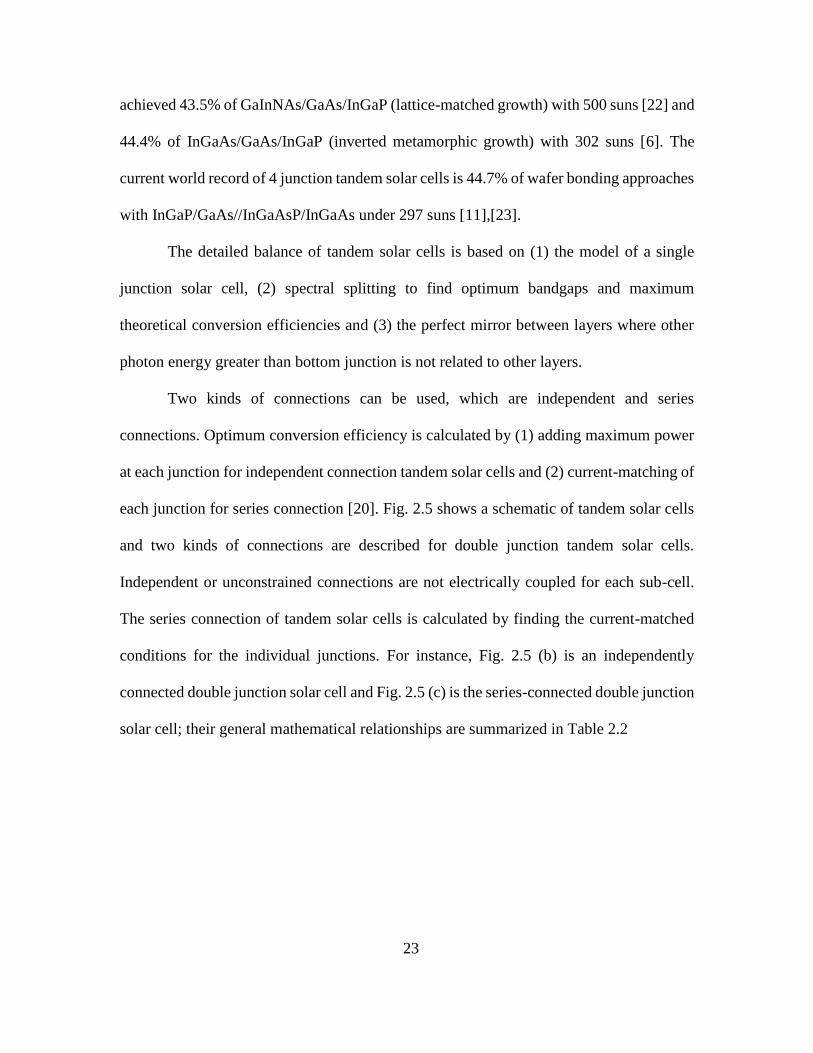
Two kinds of connections can be used, which are independent and series
connections. Optimum conversion efficiency is calculated by (1) adding maximum power
at each junction for independent connection tandem solar cells and (2) current-matching of
each junction for series connection [20]. Fig. 2.5 shows a schematic of tandem solar cells
and two kinds of connections are described for double junction tandem solar cells.
Independent or unconstrained connections are not electrically coupled for each sub-cell.
The series connection of tandem solar cells is calculated by finding the current-matched
conditions for the individual junctions. For instance, Fig. 2.5 (b) is an independently
connected double junction solar cell and Fig. 2.5 (c) is the series-connected double junction
solar cell; their general mathematical relationships are summarized in Table 2.2

24
Fig. 2.5. The schematic of tandem solar cells: (a) shows is the general schematic of
tandem solar cells, (b) shows a two-junction independent connection, and (c)
shows a two-junction series connection where Eg(i) stands for bandgap energy of
each sub-cell in tandem solar cells, and i=positive integer.
Table 2.2. The relationship of theoretical efficiencies for tandem solar cells between an
independent connection and a series-connection. J is the current density and V
is the operating voltage, Jm is the current density at maximum power point and
Vm is the operating voltage at maximum power point. Pmax is the maximum
power, and i=1,2,3…N.
Connection Current Density Operating Voltage Maximum Power
Independent
Connection
Jm,i Vm,i i,mV
N
1ii,mJmaxP
Series Connection JTotal=J1=···=JN VTotal=V1+···+VN Pmax=JTotalVTotal

25
Fig. 2.6. The spectral splitting of double junction tandem solar cells
The spectral splitting is also important to find optimum conditions of tandem solar
cells. Fig. 2.6 describes the procedure of spectral splitting in double junction tandem solar
cells under terrestrial spectrum. The dotted line in Fig. 2.6 is the boundary of solar spectrum
for a double junction tandem solar cell; above this photon energy, photons are absorbed in
the top junction and below it they are absorbed in the bottom junction(s)While shifting this
boundary point, we can obtain the conversion efficiencies and the corresponding optimum
bandgaps. At the boundary, there is a perfect mirror to split the solar spectrum. The overall
simulation results of double junction tandem solar cells are shown in Fig. 2.7 and Table
2.3 under one sun illumination.

26
Fig. 2.7. The efficiency contour of 2 junction tandem solar cells
Table 2.3. The efficiency table of double junction tandem solar cells under one sun
illumination with terrestrial spectrum (AM1.5G spectrum).
Number of Junction Eg1 (eV) Eg2 (eV) Efficiency (%)
2 (Independent connection) 0.94 1.73 46.1
2 (Series Connection) 0.95 1.61 45.7
The overall results shown in Fig 2.7 are that the contour plots of a 2J independent
connection shown in Fig. 2.7 wherein (a) is broader than that of the series-connection and
However, the series connection should be matched with the lowest current of a junction,
thereby creating its contour region as shown in Fig 2.7 (b), which is narrower than the
independent connection.
2.4 The Multiple Exciton Generation Solar Cells
The detailed balance of single junction solar cell is based on one electron-hole pair
generation per incident photon giving a maximum theoretical efficiency for photovoltaic
(PV) devices of 31 % under one sun illumination with blackbody radiation [12]. As

27
mentioned in section 2.2, the thermalization of hot carriers at the conduction band is the
largest amount of losses of single junction solar cells. Thus, if this thermalization loss can
be reduced in the solar cell, a higher efficiency can be realized.
When incoming photon energy is greater than bandgap hit is incident on a single
junction solar cell, detailed balance calculations assume that there is one EHP. This process
is shown in Fig. 2.8 (a).
Fig. 2.8. (a) Thermalization of electrons of single junction solar cells results in energy
loss and heat generation; (b) MEG has the potential to create more than one EHP
per absorbed high energy photon where Eph is the photon energy, CB is the
conduction band, VB is the valence band and I.I is the impact ionization © [2013
IEEE] [24]. (see Appendix. B)
The excess energy of the incident photons makes possible the generation of more
than two EHPs due to impact ionization. This process is called the carrier multiplication or
multiple exciton generation (MEG).
Such processes were first measured in a solar cell device by Kolondinski [13] in
1993, with a quantum efficiency over 100% from a bulk type of silicon solar cell.

28
Subsequently, Werner published the detailed balance limit of carrier multiplication for the
blackbody radiation and terrestrial spectrum under one sun. The optimum bandgaps (Eg)
are 43.6% at 0.758 eV and 44.2% and 0.7 eV under blackbody radiation and AM1.5G
respectively [14],[25]-[27] The detailed balance limit of MEG includes the quantum yield
(QY) which is stair-case step function after threshold energy which is energy over QY over
100% and its value is two times of bandgap energy [26]. It will be discussed in section 3.2
with Fig 3.2.
Compared to single junction solar cell, the assumption of one EHP generation is no
longer followed in MEG solar cells, such that a single photon can create more than two
EHPs by the impact ionization. The reverse MEG process contributes to emit one photon
emission by Auger mechanism [28]. The multi-carries interactions at the conduction band
are explained by Auger recombination. In the thermodynamics of MEG, multi-carrier
recombination can transfer energy to an electron having the highest energy state to emit a
single photon. Thus, it means that voltage is not increased by quantum yield that explains
the emitted photon energy. But, it experimentally shows many differences such as a
radiative emission, a faster generation rate than bulk Auger mechanism.
Recently, the nano-crystals or quantum dots have demonstrated the MEG effects
for high energy photons by using PbSe and PbS colloidal quantum dots over 300% of
internal quantum efficiencies with delayed the threshold energy that it is the energy of QY
over 100% [29].
A QY measurement by ultra-fast transient absorption spectroscopy shows that the
QY linearly increase after the threshold energy and its threshold energy is generally
between 2·Eg and 3·Eg [29]. But, the effect of increasing threshold energy provides the
29
huge impacts for maximum conversion efficiency and its optimum bandgap. Therefore, the
generalized detailed balance limit of MEG solar cell in the thermodynamic limit will be
discussed in the Chapter 3 with different QY (Ideal and non-ideal QY) and the change of
threshold energy.
2.5 The Intermediate Band Solar Cells
The intermediate band solar cell (IBSC) was proposed by Marti and Luque in 1997
[15]. The band structure of an intermediate band solar cell is shown in Fig 2.5 [15], where
an additional energy level (or band) is introduced into the previously forbidden band gap.
Crucially, the band has a separate quasi-Fermi level than either the conduction or valence
band.
Conventional assumptions of IBSC are (1) only radiative recombination (2) the
infinite mobility to make constant of the quasi-Fermi levels and make three separate quasi-
Femi levels (εFC, εFI and εFV ) shown in Fig 2.9, (3) no carrier extraction at intermediate band
(electrons in conduction band and holes in the valence band can only be extracted to the
ohmic contact), (4) absorption of all photon above the band gaps, (5) a perfect mirror at the
back of IBSC that the radiation generated can only escapes to the front side of illumination
(similar to tandem and single junction solar cells), (6) isotropic illumination of cell for
maximum efficiency [15].
The IB level makes it possible to generate three transitions which are (1) from
valence band to conduction, (2) valence band to intermediate band and (3) intermediate
band to conduction band. Then, two carriers at a conduction band can contribute to generate
an electrical current because of assumption (1) and (3). Fig. 2.9 shows about the band
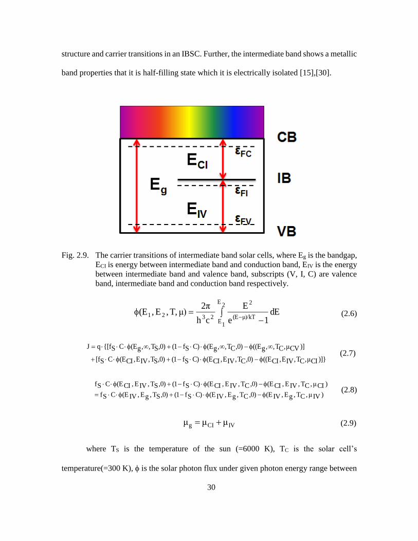
30
structure and carrier transitions in an IBSC. Further, the intermediate band shows a metallic
band properties that it is half-filling state which it is electrically isolated [15],[30].
Fig. 2.9. The carrier transitions of intermediate band solar cells, where Eg is the bandgap,
ECI is energy between intermediate band and conduction band, EIV is the energy
between intermediate band and valence band, subscripts (V, I, C) are valence
band, intermediate band and conduction band respectively.
2E
1E
μ)/kT(E
2
2321 dE1e
E
ch
2πμ)T,,E,(E (2.6)
)]}CIμ,CT,IVE,CI((E,0)CT,IVE,CI(EC)Sf1(,0)ST,IVE,CI(ECS[f
)]CVμ,CT,,g((E,0)CT,,g(EC)Sf1(,0)ST,,g(ECS{[fqJ
(2.7)
)IVμ,CT,gE,IV(E,0)CT,gE,IV(EC)Sf1(,0)ST,gE,IV(ECSf
)CIμ,CT,IVE,CI(E,0)CT,IVE,CI(EC)Sf1(,0)ST,IVE,CI(ECSf
(2.8)
IVCIg μμμ (2.9)
where TS is the temperature of the sun (=6000 K), TC is the solar cell’s
temperature(=300 K), is the solar photon flux under given photon energy range between

31
E1 and E2, i=1,2,···, fS is the geometric factor(= 1/46200) and C is the concentration of
sunlight, q is the element of charge, k is the Boltzmann constant (=1.38×10⁻²³ J/K), h is the
Plank’s constant (=6.63×10⁻³⁴ J·s), c is the speed of light (3×10⁸ m/s), E1 is the low energy
state and E2 is the high energy state. μCI is the chemical potential between conduction band
and intermediate band, μIV is the chemical potential between valence band and intermediate
band and μg is the chemical potential for bandgap.
Fig. 2.10. Efficiency vs bandgap of conventional intermediate band solar cells under fully
concentrated sunlight (C=46200) accounting for bandgap optimization.
Equations from (2.6) to (2.9) are the detailed balance equations of IBSC. To
determine appropriate intermediate band level, the generation rate and recombination rate
of between (1) valence band to intermediate band and (2) intermediate band to conductions
should be the same and it is shown in Equation (2.8). The simulation results of IBSC are
summarized in Fig. 2.10 and Table 2.4.
32
Table 2.4. The optimum bandgaps and maximum efficiency of full concentration for a
single IBSC with blackbody radiation.
ECI (eV) EIV (eV) Eg (eV) Efficiency (%)
C=46200 0.72 1.25 1.97 63.2
Table 2.5. The optimum bandgaps and maximum efficiency of conventional triple junction
solar cells for independent and series connection under full concentration with
blackbody radiation.
Tandem Eg1 (eV) Eg2 (eV) Eg3 (eV) Efficiency (%)
Independent
Connection
0.62 1.26 2.10 63.8
Series
Connection
0.60 1.14 1.82 63.1
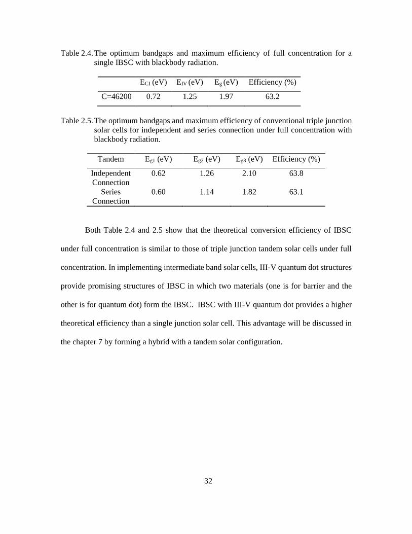
Both Table 2.4 and 2.5 show that the theoretical conversion efficiency of IBSC
under full concentration is similar to those of triple junction tandem solar cells under full
concentration. In implementing intermediate band solar cells, III-V quantum dot structures
provide promising structures of IBSC in which two materials (one is for barrier and the
other is for quantum dot) form the IBSC. IBSC with III-V quantum dot provides a higher
theoretical efficiency than a single junction solar cell. This advantage will be discussed in
the chapter 7 by forming a hybrid with a tandem solar configuration.

33
CHAPTER 3
IMPACT OF THRESHOLD ENERGY ON LIMITING EFFICIENCIES IN MULTIPLE
EXCITON GENERATION SOLAR CELLS
3.1 Introduction
Multiple exciton generation (MEG) [4],[31],[32] solar cells offer an approach to
increasing solar cell efficiency above the Schockley-Queisser limit (or single junction solar
cell limit) [12] without the need for multiple junctions. Prior to its examination for solar
cells, the generation of multiple electrons from high energy processes has been used
experimentally in several applications including impact ionization in avalanche
photodiodes; the generation of multiple carriers from a high energy electron in EBIC
(electron beam induced current measurements); and in radiation detectors [ 33]-[36].
However, these processes use excitation energies many times the bandgap, making them
unsuited for absorption from the solar spectrum. However, experimental measurement of
greater than unity quantum efficiency from light with photon energies between two to three
times the bandgap shows that multiple electrons can be generated with energies available
in the solar spectrum, with one of the first experimental demonstrations in a bulk silicon
solar cell [13].
Despite the first demonstration of carrier multiplication in silicon solar cells,
experimental results in MEG solar cells focus primarily on nanostructures and smaller
bandgaps, due to detailed balance efficiency calculations giving the optimum bandgaps at
low values [4],[31],[32]. Quantum dots are of special interest since momentum
conservation rules are relaxed, hot carrier cooling rates are potentially slowed, and
34
Coulomb coupling is greatly enhanced to increase the rate of the Auger process
[4],[31],[32]. Because of theoretical efficiency models [4],[25]-[28] which highlight the
uantum yield (the ratio of the number of carriers generated to the number of photons of a
given energy incident on the solar cell), experiments have focused heavily on the
measurement of the quantum yield (QY).
Measurements of QY in quantum dot (QD) nanostructures initially reported QYs
in a PbSe system of up to 300% [37], and measurements reported by various groups and
materials showed QYs of up to 700% [38] Material systems examined include PbS [29],
PbSe [29],[39], CdTe [40], CdSe [40],[41], InAs [42],[43], and Si [19],[44]. The initial
high reported values of QY [38] are close to those needed for ideal thermodynamic
efficiencies when a solar cell is operating at moderate concentration. However,
uncertainties in the measurement of QY due to effects such as surface states and long-lived
QD photocharging in the pump-probe measurements [45]-[51] have resulted in accepted
values up to 300% [48] in QD systems to 130% for PbSe QDs without using the transient-
absorption method [52]. These QY studies also include measurements of the threshold
energy. For example, a measurement of Si nanocrystals gives a QY of 260% and a
threshold energy of 2.4Eg,si where Eg,si is the effective bandgap of the Si nanocrystals [44].
Threshold energies of other materials range from 2.2Eg [53] to 4.2Eg [51].
The inclusion of less ideal QYs and concentration consistent with physically
realistic levels (i.e., below the maximum concentration of 46200 assumed in detailed
balance) changes the theoretical efficiency as well as the optimum bandgaps for the MEG
process. While there have been numerous detailed balance studies for MEG processes
[14],[25],[26],[54]-[56], including the impact of non-ideal QYs [54]-[56], the impact of the

35
threshold energy has examined under terrestrial spectrum. But, the blackbody radiation has
not been well examined with and without light concentration. In this chapter, the author
includes the threshold energies in detailed balance calculations, showing that there is no
theoretical benefit from MEG processes if the threshold energy is above approximately 3Eg
(for one sun) to 4Eg (for concentrated sunlight).
Fig. 3.1. (a) Thermalization of electrons of single junction solar cells results in energy
loss and heat generation; (b) Multiple Exciton Generation results in more than
one EHP per absorbed high energy photon where Eph is the photon energy, Eg is
the bandgap energy, CB is the conduction band, VB is the valence band.
Since measured values of the threshold energy are within this range, it is important
to include threshold energies in the detailed balance calculations. Further, the impact of the
threshold energy with higher concentration voids the design rule in which lower bandgaps
increase the theoretical efficiency of an MEG solar cell.

36
MEG solar cells increase the theoretical solar cell efficiency compared to a single
junction solar cell by using photons with energy at least twice the bandgap to generate two
or more electron hole pairs (EHPs). In a conventional solar cell (Fig. 3.1(a)), a high energy
excited electron relaxes to the conduction band edge and emits heat. In MEG solar cells as
shown in Fig. 3.1(b) the extra energy generates one or more additional EHPs.
3.2 Theory
The detailed balance calculations of MEG solar cells follow general detailed
balance approaches, but differ from conventional detailed balance in that the assumption
of one electron hole pair (EHP) per incident photon is circumvented. In conventional solar
cell detailed balance calculations, the QY is assumed to be unity and the reflection is zero,
giving a maximum QY of 100% for photons with energies above the bandgap and below
it.
The ideal QY of an MEG cell is step-like, such that photons with energy between
Eg and 2Eg generate a single EHP, photons with energy between 2Eg and 3Eg generate two
EHPs, and so on, as shown below:
,..3,2,1m
gEMEM
gE)1m(EgEmm
gEE00
)E(QY
(3.1)
where m is the number of multiple electron hole pairs generated, M is the maximum
number of electron hole pairs which are generated, Eg is the bandgap, and E is the photon
energy.
The value of M (the maximum number of EHPs which are generated from a photon
or the maximum QY) theoretically depends on the solar spectrum and the bandgap. For a

37
black body (BB) spectrum, M is very large, since the BB spectrum contains photons at
arbitrarily high energies, and hence even high bandgaps will encounter photons with
energies many multiples of the bandgap. However, for spectra such as AM1.5, where the
highest energy photon is at a finite energy (for AM1.5 (ASTMG 173-03 [57]) the highest
energy photon is 4.428 eV), the maximum number of EHPs which can be generated
depends on the bandgap. Fig. 3.2 (a) shows the ideal QY vs. photon energy for three
bandgaps, showing that M=7 at Eg = 0.56 eV, while for a bandgap of Eg=1.68 eV,
theoretically M = 2 (i.e., at most two electron hole pairs can be generated).
Fig. 3.2. (a) Ideal QY for three different bandgaps under the AM1.5 spectrum and (b)
non-ideal QY with A=1 for one value of Eg (=1.12eV) and three different
threshold energies.
Experimentally, measured QYs diverge from the ideal QY because: (1) the
threshold energy for a multiple exciton generation event is Eth = r·Eg where r≥2 is a real
number and (2) rather than displaying a step-function shape, experiments show a linear

38
increase in the QY with energy. The equation for non-ideal QY is given in equation (3.2)
[54].
),..gE
thEE()thE,E(A)gE,E()E(QY
(3.2)
where θ is the heaviside step function; A is the slope of the linearized QY (in terms
of QY and the photon energy normalized to Eg), Eg is the bandgap; and Eth is the threshold
energy for a MEG event.
The non-ideal QY in Fig. 3.2 (b) shows that the threshold energy has a large impact
on the maximum QY. For example, for the AM1.5 spectrum, and a threshold energy Eg =
2Eg, M retains the same value as in the ideal case, but the maximum QY is reduced to 2
with a threshold energy of three times the bandgap (see Fig. 3.2(b) green and red lines).
For this bandgap, there is no impact from MEG processes (i.e., M=1) when Eth = 4Eg.
Further, although the ideal slope A is 1, experimental measurements are best fit
using less ideal values [54]. The impact of the slope vs stair-case QY has been examined
in detailed balance [54] but not the impact of threshold energy. In this chapter, the author
includes the effect of non-ideal threshold energies in detailed balance calculations.
Particularly for the case of AM1.5 and under concentration, the threshold energy has a
dominant impact on the efficiency and optimum bandgap at A=1.
Using the above non-ideal equations for QY, the theoretical thermodynamic
equations for the MEG solar cell are given below, where equation (3.5) is the current
density for BB radiation and equation (3.6) is that for a terrestrial spectrum.
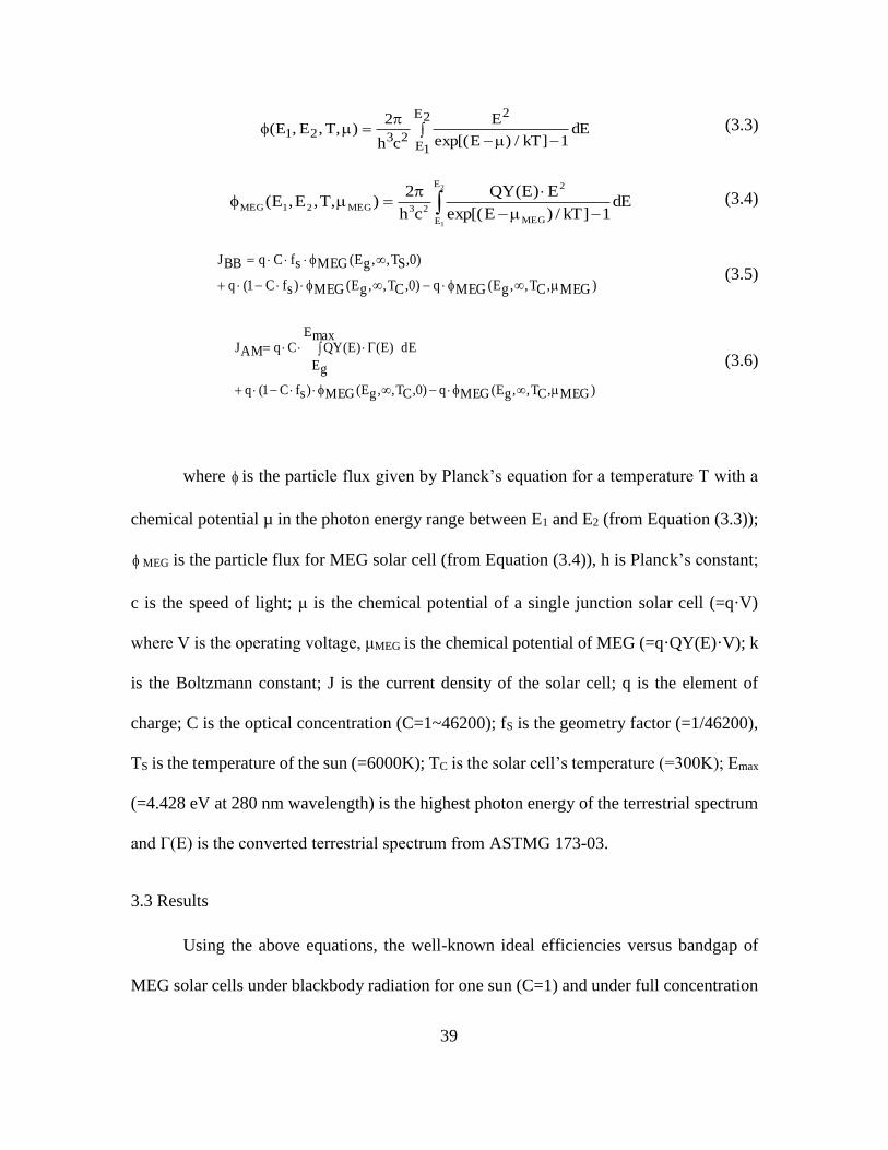
39
2E
1E
2
2321 dE1]kT/)Eexp[(
E
ch
2),T,E,E( (3.3)
2
1
E
E MEG
2
23MEG21MEG dE1]kT/)Eexp[(
E)E(QY
ch
2),T,E,E( (3.4)
)MEG,CT,,gE(MEGq)0,CT,,gE(MEG)sfC1(q
)0,ST,,gE(MEGsfCqBBJ
(3.5)
)MEG,CT,,gE(MEGq)0,CT,,gE(MEG)sfC1(q
maxE
gE
dE)E()E(QYCqAMJ
(3.6)
where is the particle flux given by Planck’s equation for a temperature T with a
chemical potential µ in the photon energy range between E1 and E2 (from Equation (3.3));
MEG is the particle flux for MEG solar cell (from Equation (3.4)), h is Planck’s constant;
c is the speed of light; μ is the chemical potential of a single junction solar cell (=q·V)
where V is the operating voltage, μMEG is the chemical potential of MEG (=q·QY(E)·V); k
is the Boltzmann constant; J is the current density of the solar cell; q is the element of
charge; C is the optical concentration (C=1~46200); fS is the geometry factor (=1/46200),
TS is the temperature of the sun (=6000K); TC is the solar cell’s temperature (=300K); Emax
(=4.428 eV at 280 nm wavelength) is the highest photon energy of the terrestrial spectrum
and Г(E) is the converted terrestrial spectrum from ASTMG 173-03.
3.3 Results
Using the above equations, the well-known ideal efficiencies versus bandgap of
MEG solar cells under blackbody radiation for one sun (C=1) and under full concentration

40
(C=46200) are shown in Fig. 3.3 (a) and (b) respectively as a function of M. Compared to
existing literature, the author repeats these plots with an extended number of calculations
for M in order to identify the M value after which no further efficiency increase is
calculated. For the one-sun BB case, the maximum efficiency is saturated after M=13 (i.e.,
a total of 13 EHPs generated from the high energy photons) and the conversion efficiency
is 44.7% at Eg=0.77 eV. At full concentration, the maximum conversion efficiency is
85.9% at Eg = 0.05 eV at M=200.
Fig. 3.3. Efficiency vs Eg with ideal QY for one sun and maximum concentration for
Blackbody Radiation and terrestrial spectrum where M is the maximum QY.
The ideal MEG solar cells efficiencies for the AM1.5 spectrum under one sun and
under maximum concentration are shown in Fig. 3.3 (c) and (d). For one sun illumination,
the conversion efficiency is saturated at M=5 for which Eg = 0.7 eV. A QY = 300%

41
(corresponding to M=3), which is consistent with experimental measurements of QY,
should allow close to ideal theoretical efficiencies. At maximum concentration, the
conversion maximum efficiency is 79.8% at Eg = 0.31eV and M = 14. In Fig. 3.3 (c) and
(d) there are no values plotted below 0.3 eV as there are no photons in the AM1.5 spectrum
below this value, and reducing the bandgap below the lowest photon energy only degrades
efficiency.
Fig. 3.4. Efficiency vs Eg for non-ideal QY as a function of threshold energy under both
one sun and full concentration (Blackbody radiation and terrestrial spectrum)
Fig. 3.4 shows the theoretical efficiency with non-ideal QYs for BB and AM1.5
spectra. Eth = 2Eg corresponds to the ideal threshold energy, and QY is linearly increased
(A=1) after 2Eg. For these calculations, there is no limit placed on the maximum ideal QY
values as there is for the ideal QY calculations above.
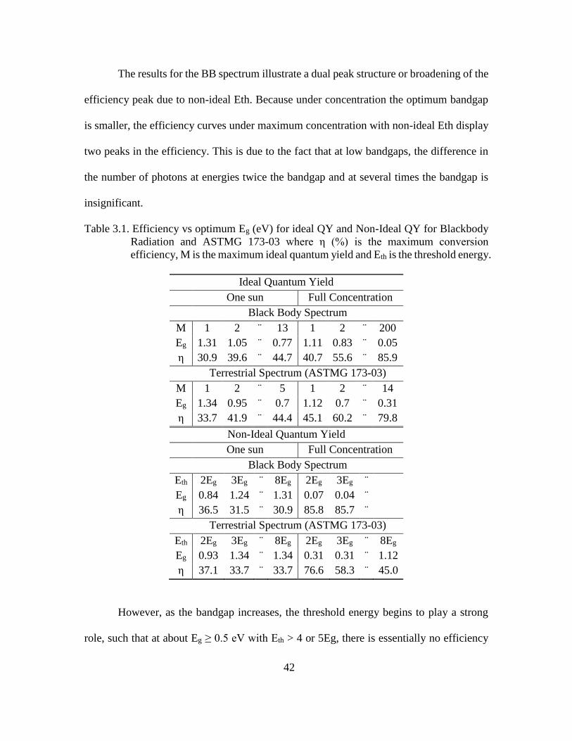
42
The results for the BB spectrum illustrate a dual peak structure or broadening of the
efficiency peak due to non-ideal Eth. Because under concentration the optimum bandgap
is smaller, the efficiency curves under maximum concentration with non-ideal Eth display
two peaks in the efficiency. This is due to the fact that at low bandgaps, the difference in
the number of photons at energies twice the bandgap and at several times the bandgap is
insignificant.
Table 3.1. Efficiency vs optimum Eg (eV) for ideal QY and Non-Ideal QY for Blackbody
Radiation and ASTMG 173-03 where η (%) is the maximum conversion
efficiency, M is the maximum ideal quantum yield and Eth is the threshold energy.
Ideal Quantum Yield
One sun Full Concentration
Black Body Spectrum
M 1 2 ¨ 13 1 2 ¨ 200
Eg 1.31 1.05 ¨ 0.77 1.11 0.83 ¨ 0.05
η 30.9 39.6 ¨ 44.7 40.7 55.6 ¨ 85.9
Terrestrial Spectrum (ASTMG 173-03)
M 1 2 ¨ 5 1 2 ¨ 14
Eg 1.34 0.95 ¨ 0.7 1.12 0.7 ¨ 0.31
η 33.7 41.9 ¨ 44.4 45.1 60.2 ¨ 79.8
Non-Ideal Quantum Yield
One sun Full Concentration
Black Body Spectrum
Eth 2Eg 3Eg ¨ 8Eg 2Eg 3Eg ¨
Eg 0.84 1.24 ¨ 1.31 0.07 0.04 ¨
η 36.5 31.5 ¨ 30.9 85.8 85.7 ¨
Terrestrial Spectrum (ASTMG 173-03)
Eth 2Eg 3Eg ¨ 8Eg 2Eg 3Eg ¨ 8Eg
Eg 0.93 1.34 ¨ 1.34 0.31 0.31 ¨ 1.12
η 37.1 33.7 ¨ 33.7 76.6 58.3 ¨ 45.0
However, as the bandgap increases, the threshold energy begins to play a strong
role, such that at about Eg ≥ 0.5 eV with Eth > 4 or 5Eg, there is essentially no efficiency

43
benefit from MEG processes- in this bandgap range, the MEG solar cell is the same as a
conventional device. At moderate threshold energies, the conversion efficiency vs.
bandgap corresponds to a combination of the ideal MEG efficiency curve at low bandgaps
and the ideal single junction efficiency curve at higher bandgaps. A similar effect is shown
for the non-ideal MEG efficiencies at AM1.5, but with the convergence between the MEG
and conventional solar cell occurring at lower Eth.
The key values of M, Eth, Eg, and efficiency are summarized in Table 3.1, and
highlight the impact on optimum bandgap and efficiency of including threshold energy in
the calculations. First, as expected with the inclusion of non-idealities, the overall
efficiency is lower. For example, comparing the ideal M=2 case with that of the linear QY
and Eth = 2Eg under one sun illumination, the optimum efficiency is 36.5% in BB and
37.1% in AM1.5 instead of 39.6% in BB and 41.9%. Further, there is a substantial drop in
the conversion efficiency with threshold energies consistent with experimental values in
the range between 2Eg and 3Eg. At 3Eg, the maximum efficiency under one sun is
essentially identical to a single junction solar cell, with no theoretical benefit derived from
the MEG process, regardless of what the maximum QY is assumed to be.
Another substantial difference observed with the inclusion of Eth is the value of the
optimum bandgap for MEG cells. In ideal QY calculations, an efficiency increase from the
MEG process exists even for bandgaps up to about 0.5 eV, but when a higher Eth is
considered, the efficiency benefits are strongly reduced at higher bandgaps. Ideal BB MEG
calculations give an optimum Eg =0.05 eV at maximum concentration. While such low
bandgaps are not realistic, in general the results show a slowly increasing optimum
bandgap depending on the maximum QY. However, the dual peak (or peak broadening for
44
lower concentration) voids this design rule, with the efficiency decreasing unless Eg <0.5
eV and Eth < 4Eg are assumed. At maximum concentration with the terrestrial spectrum,
after the threshold energy exceeds 4Eg, the maximum efficiency and optimum Eg is fixed
at 45.0 % and Eg = 1.12 eV. Typical measurements of threshold energies are on the order
of from 2Eg to 3Eg, which is significant since it leads to a theoretically predicted optimum
bandgap range that includes commonly used semiconductors for solar cells, including
silicon.
3.4 Conclusion
In summary, the author has applied a generalized detailed balance model to MEG
solar cells. For this simulation, using both ideal and non-ideal QYs the author calculates
and compares conversion efficiencies under blackbody and terrestrial solar spectrum
irradiation with and without concentration. Like the cases with ideal QYs, the optimal
parameters (Eg and η) of non-ideal QYs (with ideal threshold energies and maximum
concentration) show that the author can choose extremely low bandgap materials for MEG
solar cells. However, the conversion efficiency and optimum bandgap are strongly
dependent on the threshold energy, and the value of the efficiency for low material
bandgaps is particularly sensitive to such non-idealities. For intermediate concentration
and values of the threshold energy above Eth = 3Eg, the efficiencies and the optimum
bandgaps are essentially identical to those without MEG processes.
45
CHAPTER 4
LIMITING EFFICIENCIES OF MULTIJUNCTION SOLAR CELLS WITH
MULTIPLE EXCITON GENERATIONS
4.1 Introduction
A number of approaches have been proposed to overcome the detailed balance
single junction efficiency limits calculated by Shockley and Queisser [12], including
multiple junction solar cells and novel concepts such as multiple exciton generation (MEG)
and intermediate band solar cells [15],[21],[58]. Multijunction (MJ) solar cells have been
commercialized and demonstrate high efficiencies. However, the realization of efficiencies
over 50% via conventional tandem approaches requires increasing the number of junctions
in the solar cells from the present three junctions (3J) to at least four junctions (4J),
introducing substantial materials challenges [59]. By including MEG processes into MJ
solar cells [60], both the number of junctions and materials constraints are relaxed allowing
efficiencies over 50% with a 2J and 3J device. © [2014 IEEE] [61](see Appendix. B)
4.2 Multijunction Solar Cells with MEG Process
Since MJ solar cells were first proposed by Jackson [ 62 ] in 1955, steady
improvements in efficiencies have been achieved, initially through mechanical stacks (e.g.,
AlGaAs and Si demonstrating 28.5% at AM 1.23 165 suns in 1978 [63]), and later through
monolithic structures, with most of the focus on a three junction MJ on a Ge substrate. Two
junction tandem photovoltaic devices demonstrated over 30% under 140~180 suns in 1994
[64],[65] and a triple junction tandem solar cell broke the 40% barrier under 240 suns [66]
in 2007 using both lattice-matched (LM) and mismatched configurations. Since then, high

46
efficiency device structures have diversified, with a range of approaches realizing over 40%
efficiency [67]-[72]. Current triple junction solar cells show 43.5% and 44.4% using dilute
nitride (GaInNAsSb/GaAs /InGaP) LM approaches and InGaP/GaAs/InGaAs [6],[22]
respectively.
Despite numerous experiments showing MJ devices over 40%, MJ solar cells still
face barriers in reaching 50% efficiency, due to a larger required number of junctions
(minimum 4J in order to achieve 50%); material defects (due to metamorphic or other
growth approaches); and limited material combinations and structures that have
appropriate growth technologies [73],[74]. For instance, even though the detailed balance
calculations for a triple junction solar cell under one sun show a conversion efficiency over
50% [20],[58],[75],[76], the experimental results are about 10% absolute efficiency points
lower. This is largely due to the inability to grow a monolithic structure with the optimum
bandgaps using only closely lattice matched materials. The resulting non-optimum
bandgaps give rise to current mismatches [77], and since the junctions are series connected,
the overall MJ’s current is limited to the lowest current. One approach to avoid this
combines two solar cells with 2J each mechanically, but this represents a significant
departure from existing structures [78].
An fundamental discussion of MEG solar cells have discussed in chapter 3 about
the MEG phenomena, detailed balance limit and experimental approaches
[13],[14],[25],[26],[79]-[81],[29],[41],[82],[83]. For a multijunction solar cells with MEG,
the detailed balance for MJMEG is discussed in section 4.3.
A quantum yield over 100% has been measured in bulk silicon solar cells [13], and
nanostructured materials have shown an enhanced MEG effect with quantum yields up to

47
300% [81]-[83]. An attractive aspect of MEG solar cells is that they allow the use of low
bandgap materials. Therefore, it is of interest to integrate MEG concepts with MJ solar
cells and recalculate the optimum bandgaps (Eg) to determine if this enables the use of
practical materials while improving the theoretical efficiencies [60].
In this chapter, the author analyze the thermodynamic limits for MJ hybrid MEG
solar cells (MJMEGs), calculating the theoretical maximum efficiency and finding the
optimum bandgaps under both blackbody (BB) radiation and the terrestrial spectrum at
both one sun illumination and maximum concentration.
4.3 Theory
4.3.1 Detailed Balance Calculations Including MJMEG
Thermodynamic models of multiple junction solar cells and multiple exciton
generation are well documented in literature [14],[20],[25]-[28],[75],[76],[79]-[81].
Thermodynamic models of a single junction solar cell consider absorption of the solar
spectrum using one bandgap and one electron and hole pair (EHP) generation per photon
[12], whereas MJ solar cells have multiple bandgaps, dividing the solar spectrum among
the different junctions in the stack [20],[75],[76]. An example of this spectral splitting is
shown in Fig.4.1 (a) for a 4J solar cell, dividing the spectrum into 4 different bandgaps.
In detailed balance calculations for MEG devices, the author typically use ideal
assumptions from detailed balance as described in [25]-[28] which state that a MEG solar
ell is perfectly ideal photovoltaic device (100% absorption above band gap, recombination
at the thermodynamic limit) in which there are multiple EHPs generated for a high energy
photon and multi-particle recombination events emit a single photon [25]-[28].

48
Fig. 4.1. Spectral splitting and QY in conventional MJ and MJMEG solar cells. (a) A four
junction MJ solar cell. The QY of each region is 1. (b) Ideal QY for a
multijunction device with MEG © [2014 IEEE] [61].
49
The main difference between conventional single junction or MJ and MEG solar
cells is the number of EHPs generated from a particular photon wavelength or energy. The
generated number of EHPs is given by the quantum yield (QY). For single junction or
conventional MJ cells, QY =1 as shown in Fig.4.1 (a), but for MEG cells QY can exceed
one.
In ideal MEG devices, the QY is one for photons with energies between the
bandgap and twice the bandgap (2Eg), two for photons of energy greater than 2Eg but less
than 3Eg, and so on, giving in the ideal case a staircase function for the QY [60]. The
equation for the ideal QY of any junction in an MJMEG cell is given by:
)QYMaximum(M,3,2,1mwhere
EgEMM
gE)1m(EgEmm
gEE00
)E(QY
(4.1)
From equation (4.1), the author defines M as the maximum value of m (i.e., the
maximum number of generated EHPs) within a junction. The remaining equations in the
detailed balance calculations are given in equation (4.2) to (4.5). These equations and their
constants have their usual form and definition of constants as in [20],[25]-
[28],[60],[75],[76]. The notation Ji, µi, Ei etc refers to the “ith” junction, and the “i+1”th
unction is the junction with above the “ith” cell in the MJMEG solar cell stack where
i=1,2,3…. . For a solar cell with n total junctions, the “n+1” energy in the integral limits is
replaced by infinity when using a BB spectrum or the highest photon energy in the AM1.5
spectrum when using this input solar spectrum.
50
)1i(E
)i(EdE
1]kT/)Eexp[(
2E)E(QY
2c3h
2),T,)1i(E,)i(E( (4.2)
)i,CT,)1i(gE,)i(gE(q
)0,CT,)1i(gE,)i(gE()sfC1(q
)0,ST,)1i(gE,)i(gE(sfCqBB,iJ
(4.3)
)i,CT,)1i(gE,)i(gE(q
)0,CT,)1i(gE,)i(gE()sfC1(q
)1i(gE
)i(gE
dE5.1AM)E(QYCq5.1AM,iJ
(4.4)
iV)E(QYqi (4.5)
where is the particle flux of MEG given by Planck’s equation for a temperature T
with a chemical potential µ(=q·QY(E)·V) in the photon energy range between E(i) and E(i+1),
ГAM1.5 is the terrestrial spectrum from ASTMG 173-03, h is the Plank's constant, c is the
speed of light, k is Boltzmann's constant, TS is the temperature of the sun, TC is the
temperature of the solar cell, fS is the geometry factor (=1/46200), and C is the
concentration, V is the operating voltage.
Detailed balance involves the calculation of the current from the solar cell as the
difference between the absorbed and emitted photon fluxes. Equation (4.2) is the definition
of the either absorbed or emitted photon flux for a MEG solar cell. Equation (4.3) and (4.4)

51
correspond to the current generated by an MEG solar cell for the BB and AM1.5 spectrum
respectively for the ith solar cell in the MJMEG. The first two flux terms correspond to
photons absorbed from the solar spectrum. If the ith solar cell absorbs photons with more
than twice its band gap (which depends on the other solar cell band gaps in the stack), the
light generated current is increased compared to a conventional MJ solar cell.
The last term of equation in (4.3) and (4.4) corresponds to the emitted photon flux.
The emitted photon flux is changed in an ideal MEG device compared to conventional
single junction solar cell, in that the inverse of the MEG process must also occur [25]-[28].
hus, in the calculation of the emitted photon flux, the “i” in equation (4.5) is modified
from its definition compared to a conventional single junction or multijunction solar cell.
In a conventional single junction or multijunction solar cell, it corresponds to the chemical
potential, the quasi-Fermi level separation or the voltage across the device (µ´=q·V). In an
MEG process, this is replaced by m´, where m depends on the energy as given in (1).
Physically, the QY(E) term in the emission process accounts for the use of more than two
EHPs in the emission process and equation (4.5) accounts for the increased energy of the
emitted photon (e.g., twice or more the bandgap) [25]-[28]. Overall, for MEG devices, the
m´ term in the emitted flux terms does not mean that the voltage measured from the solar
cell is increased m times but rather accounts for the increase in the energy of the emitted
photons.
Conventionally, the inclusion of multiple carriers recombination processes as
describe above is termed as Auger recombination, and corresponds to the thermodynamic
limit for a multiple EHPs interaction in recombination [28]. Because of the similarity to
Auger recombination (e.g., multiple electron hole pairs are generated from a single

52
recombination event) or inverse impact ionization, the MEG detailed balance calculations
are considered to include Auger recombination. However, there are in practice multiple
differences between such a thermodynamic process and measured Auger processes,
including radiative emission and faster generation rates from the proposed multiple EHPs
process compared to the rate of conventional bulk Auger recombination [82],[84].
Overall, Auger mechanism in equation (4.1) to (4.5) and [25]-[28] is the
thermodynamic limit term; conventional Auger coefficients typically include other
multiple carrier interaction and would have different Auger coefficients, leading to higher
recombination [43],[84]. Further discussion of QY in MJMEG has explained in Appendix
C.
4.3.2 Spectral Splitting in MJMEG Solar Cells
A key difference between a conventional MJ and a MJMEG solar cell is that the
quantum yield can exceed unity. In a single junction MEG solar cell, the ideal maximum
QY can be high, and the highest efficiencies assume QY over 800%. For the case of a BB
spectrum, the theoretical QY can be arbitrarily high, as the spectrum contains at least some
photons with an energy many times the bandgap. The maximum QY is lower for the
terrestrial AM0 or AM1.5 spectra, which have a defined upper energy limit. In this case,
the maximum QY is determined by the bandgap of the solar cell. For example, with
bandgap of 0.5 eV, the maximum QY for the AM1.5 spectrum (in which the highest energy
photon is 4.42 eV) is 800%; for an absorber material bandgap of 1.0 eV, the maximum QY
is 400%.
In a MJMEG solar cell, unlike a single junction MEG, the maximum quantum yield
is limited by the next higher bandgap. For example, if the lowest bandgap is 0.5 eV and the

53
next bandgap is 0.9 eV, then the maximum QY is 1, and there is no theoretical increase
from MEG processes. If the bandgap combinations are 0.5 eV and 1.2 eV, then photons
with energies between 1.0 and 1.2 eV can generate two EHPs in the 0.5 eV solar cell.
Overall, if there is a wide spacing between the bandgaps of the MJ device, then each solar
cell in the stack can absorb photons with energies at least twice its bandgap.
Fig. 4.1 (b) shows this ideal calculated QY for a 4J solar cell with bandgaps of 0.31
eV(=Eg1), 0.93 eV(=Eg2), 1.86 eV(=Eg3) and 2.79 eV(=Eg4). Each junction has a possible
maximum QY of 200%. In the absence of the higher bandgap junctions, the lowest bandgap
junction could generate 3 electron hole pairs at photon energies above 0.93eV; however,
no 0.93 eV photons strike the bottom cell since these are all absorbed by the solar cell
above it.
The example shown in Fig.4.1 (b) explains why the number of junctions for which
MJMEG solar cells demonstrate efficiency advantages is constrained. As the number of
junctions increases, the benefit from MEG processes disappears because the maximum QY
of any junction is limited by the photon energy resulting from the spectral splitting. Overall,
to take advantage of MEG within each junction, the threshold of photon energy is two times
greater than the lower photon energy (Eg(i+1)>2Eg(i)) assuming two EHPs per one photon.
4.4 Results
The author have calculated the limiting efficiencies of up to 4 junction MJ and
MJMEG solar cells, for BB and AM1.5 spectra with either series or independent
connections. For the AM1.5 spectrum, AM1.5G is used for the one-sun calculations and
AM1.5D for the concentrated solar calculations. The efficiency contour plots for 2J solar

54
cells are shown in Figs. 4.2-4.4 for BB and Figs. 4.5-4.6 for AM1.5 spectra; Fig. 4.7 gives
the plot for 2 J and 3J solar cell at 900 suns. The BB simulation is included as they more
clearly highlight the trends due to the absence of local maxima and minima caused by the
absorption bands in the AM1.5 spectrum.
Tables 4.1 and 4.2 give the results for the optimum bandgaps for 2J to 4J MJ and
MJMEG solar cells for one sun, and Table 4.3 and 4.4 show the results for full
concentration. The series-connected case is the most relevant, as this typically implemented
for monolithic devices. The optimum bandgap values and efficiency are also given for
independent connections, particularly given increasing focus on spectral splitting
approaches which can use independently connected solar cells.
Table. 4.1. Independent connection for MJ and MJMEG (BB and AM1.5G, One sun)
where BB is the blackbody radiation and AM is the terrestrial spectrum, η is the
maximum conversion efficiency © [2014 IEEE] [61].
Eg1 (eV) Eg2 (eV) Eg3 (eV) Eg4 (eV) η (%)
2(MJ) BB 0.98 1.87 42.9
AM 0.94 1.73 46.1
2(MJMEG) BB 0.68 1.76 47.8
AM 0.70 1.82 48.8
3(MJ) BB 0.82 1.43 2.25 49.3
AM 0.93 1.42 2.08 52.0
3(MJMEG) BB 0.60 1.49 2.13 51.3
AM 0.69 1.24 2.25 52.8
4(MJ) BB 0.72 1.21 1.77 2.55 53.3
AM 0.70 1.13 1.64 2.25 56.0
4(MJMEG) BB 0.54 1.31 1.81 2.47 54.1
AM 0.70 1.13 1.64 2.25 56.0

55
Table 4.2. Series Connection for MJ and MJMEG (BB and AM1.5G, One sun), © [2014
IEEE] [61]
Eg1 (eV) Eg2 (eV) Eg3 (eV) Eg4 (eV) η (%)
2(MJ) BB 0.98 1.70 42.5
AM 0.95 1.61 45.7
2(MJMEG) BB 0.64 1.46 47.3
AM 0.57 1.38 47.8
3(MJ) BB 0.83 1.31 1.96 48.6
AM 0.93 1.36 1.90 51.4
3(MJMEG) BB 0.75 1.26 1.95 50.6
AM 0.70 1.20 1.80 51.8
4(MJ) BB 0.70 1.11 1.53 2.14 52.5
AM 0.71 1.11 1.49 2.00 55.3
4(MJMEG) BB 0.71 1.10 1.53 2.16 53.7
AM 0.71 1.11 1.49 2.00 55.4
Table 4.3. Independent Connection for MJ and MJMEG (BB and AM1.5D, C=46200),
© [2014 IEEE] [61]
Eg1 (eV) Eg2 (eV) Eg3 (eV) Eg4 (eV) η (%)
2(MJ) BB 0.77 1.70 55.8
AM 0.70 1.53 60.4
2(MJMEG) BB 0.46 1.42 66.7
AM 0.47 1.34 68.3
3(MJ) BB 0.62 1.26 2.10 63.7
AM 0.70 1.34 1.99 67.9
3(MJMEG) BB 0.45 1.38 1.95 69.7
AM 0.49 1.44 2.08 72.2
4(MJ) BB 0.52 1.03 1.61 2.41 68.7
AM 0.51 0.95 1.49 2.13 72.6
4(MJMEG) BB 0.42 1.27 1.95 2.38 72.4
AM 0.48 1.38 1.82 2.33 75.2

56
Table 4.4. Series Connection for MJ and MJMEG (BB and AM1.5D, C=46200), © [2014
IEEE] [61]
Eg1 (eV) Eg2 (eV) Eg3 (eV) Eg4(eV) η (%)
2(MJ) BB 0.76 1.54 55.5
AM 0.70 1.44 60.4
2(MJMEG) BB 0.42 1.25 66.6
AM 0.46 1.22 67.9
3(MJ) BB 0.60 1.14 1.82 63.2
AM 0.69 1.17 1.74 67.7
3(MJMEG) BB 0.40 0.95 1.72 67.1
AM 0.35 0.94 1.58 68.7
4(MJ) BB 0.49 0.93 1.38 2.01 67.8
AM 0.54 0.98 1.39 1.90 71.8
4(MJMEG) BB 0.36 0.81 1.30 1.97 69.8
AM 0.53 0.97 1.37 1.88 71.9
The figures and tables show that in all cases the MJMEG hybrid solar cells have
higher efficiencies than the corresponding MJ solar cell. Further, as expected from the QY
discussion above, the efficiency benefit is larger when the number of junctions in the stack
is smaller and under higher concentration. For example, Table 4.2 shows that for a 4J solar
cell, the difference between a MJ and a MJMEG is 0.1% at one sun (AM1.5G), while it is
7.5% absolute for a 2J solar cell under concentration (AM 1.5 D) in Table 4.4.
While MJMEG solar cells have a higher efficiency, two additional advantages are
the impact of MEG on the optimum bandgaps and the sensitivity of the efficiency to the
bandgaps. The net effect is that it allows higher efficiencies with bandgaps in the range of
existing III-V materials.

57
4.4.1 Impact on Optimum Bandgaps
The inclusion of MEG processes in a MJ solar cell has a relatively large impact on
the optimum bandgaps, particularly junctions. The figures and tables show that the lowest
optimum bandgap shifts to lower energies. This is best illustrated graphically in Figs 4.2
to 4.6, where in comparing each set of plots, the highest efficiency region illustrated by
dark red shifts to lower energies. Similarly, Table 4.2 shows that a conventional 2J series
connected solar cell has an optimum lowest bandgap of 0.95 eV under one sun AM1.5
conditions, whereas including MEG effects decreases the optimum bandgap to 0.57 eV.
Including concentration further reduces the optimum band gap to 0.46 eV (Table 4.4).
The lower optimum bandgaps and its decreasing value with concentration are
caused by two effects. These trends are consistant with single junction MEG results, which
also have substantially higher efficiencies under concentration. This can be understood in
that the optimum bandgaps for MEG processs are lower than those for a conventional
device. However, for lower bandgaps, the difference between the quasi-Fermi level
separation and the bandgap is a comparatively large fraction. As this difference is reduced
with concentration, the propreties of MEG devices improve strongly with concentration.
A second cause of the reduced bandgaps is that MEG will only provide a benefit if
the solar cell absorbs light of energy at least twice its bandgap. This has the effect of
increasing the spread of bandgaps, particularly decreasing the lowest bandgap.
Even so, several of the MJMEG devices do not have MEG processes in all of the
component solar cells. For example, from Table 4.3, the bandgap of the second junction of
a triple junction

58
Fig. 4.2. Efficiency contour for a 2J MJ and MJMEG hybrid at one sun, BB spectrum
independently connected © [2014 IEEE] [61].
Fig. 4.3. Efficiency contour for a 2J MJ and MJMEG hybrid at one sun, BB spectrum
series connected, © [2014 IEEE] [61].
Fig. 4.4. Efficiency contour for a 2J MJ and MJMEG at maximum concentration, BB
spectrum series connected, © [2014 IEEE] [61].

59
Fig. 4.5. Simulated efficiency contour for a 2J MJ and MJMEG hybrid at one sun,
AM1.5G spectrum, series connected, © [2014 IEEE] [61].
Fig. 4.6. Simulated efficiency contour for a 2J MJ and MJMEG hybrid at maximum
concentration, AM1.5D spectrum, series connected, © [2014 IEEE] [61].
MJMEG is Eg2=1.38 eV for a BB spectrum. In order to benefit from MEG processes,
the highest bandgap should be greater than 2.76 eV; however, this is higher than the
optimum bandgap (=1.95 eV) of the third junction so the middle solar cell does not benefit
from MEG processes.
4.4.2 Impact on Sensitivity of Efficiency to Bandgap
An important advantage of the MJMEG compared to the MJ solar cell is the
increased flexibility in choosing bandgaps. The double junction MJMEG contour plots

60
(Figs 4.2-4.6) show this effect graphically; a 3J 3-dimensional plot displays similar effects
(Fig.4.7). Figs 4.2-4.4 show that the optimum bandgap ranges somewhat to smaller
bandgap values) and a second larger "tail" region at substantially lower values, particularly
for the lowest band gap. Taken together, these two regions greatly expand the possible
bandgaps which give high efficiencies.
Similar effects are seen for 2J solar cells under a AM1.5 spectra, although
comparing the MJ and MJMEG the "tail" is less evident due to "ragged" contours resulting
from the absorption peaks in the AM1.5 spectra. For example, Fig.4.5 shows that a
conventional 2J device has an optimum bottom junction bandgap between 0.9 and 1.0 eV;
the MJMEG device has an optimum bottom junction bandgap between 0.4 eV and 1.2 eV.
Similar effects are shown in Fig. 4.6 under concentration, with optimum bottom band gaps
ranging from 0.3 eV to 0.9 eV.
The contour plots and tables show several important features. The optimum
bandgaps (Table 4.2 and 4.4 for series connected one sun and maximum concentration)
show lower optimum band gaps. For example, under one-sun, the optimum bandgaps are
0.7 eV, 1.2 eV, and 1.8 eV for the MJMEG device. 0.7 eV fits well with the typically used
Ge substrate.
In addition to the increased range of bandgaps, the efficiencies of two or three
junction MJMEG solar cells under concentrated sunlight conditions are larger than
conventional three or four junction MJ solar cells. For instance, the maximum conversion
efficiency of double junction MJMEG solar cells under full concentration is greater than
that of conventional triple junction MJ solar cells. From these results, the author expect

61
that better efficiency MJMEG solar cells can be made with fewer junctions compared to
conventional MJ solar cells when operated under concentrated conditions.
4.4.3 The Discussion of 2J and 3J MJMEG Devices under 900 Suns
Fig. 4.7. Simulated efficiencies of series-connected 2J(=(a),(b)) and 3J(=(c), (d))MJ and
MJMEG solar cells under 900 suns. Eg1 and Eg2, Eg2 and Eg3 and Eg3 and Eg1
planes are used to plot in Fig.7 (c) and (d) © [2014 IEEE] [61].
As an example with moderate concentration, the author calculate efficiencies for
both 2J and 3J MJ and MJMEG devices under 900 suns with the terrestrial spectrum and
display the results in Fig. 4.7. Fig. 4.7 (a) and (b) present results for 2J cells. The maximum
62
efficiency is 60.9% with optumum bandgaps of 0.47 eV(=Eg1) and 1.24eV (=Eg2) in 2J
MJMEG devices, changed from the optimum values of 2J MJ cells (0.7(=Eg1) and 1.44
eV(=Eg2)) with 54.3%). These optimum MJMEG bandgaps are well matched with InAs
(bottom junction) and Si or InP (top junction).
3J MJ and MJMEG device results are highlighted in Fig. 4.7 (c) and (d). At
concentration levels approaching 1000X, the plots in Fig. 4.7 (d) show efficiencies of 60%
for cells with bandgaps which are lattice matched to InP; lattice matched device structures
for 4J cells can also be fabricated with efficiencies close to optimum. For example, for a
3J MJMEG, potential materials include InAs (=0.36 eV)/ AlGaSb (=1eV)/ and AlAsSb or
AlSb (=1.6eV) to give a maximum theoretical efficiency of 59.3%. Another approach using
InP can show a good efficiency (54.7%) with InGaAs (=0.65eV)/ InP(1.34 eV)/AlAsSb or
InAlAs (=1.9eV). These materials are significant since they allow optimum 3J and 4J
monolithically grown solar cells using materials (e.g., InP and InAs) for which MEG
phenomenon have been shown by ultrafast transient absorption measurements [83],[84].
The material selection for the bottom junction is especially critical if one is to achieve good
carrier confinement in the quantum dots necessary for efficient MEG.
4.5 Conclusion
Hybrid solar cells combining multijunction solar cells with MEG to enhance the
entire performance of multijunction solar cells offer higher theoretical efficiencies and a
broader material space. Importantly, these efficiencies can be achieved with a maximum
MEG QY of 200%, a range which has been experimentally demonstrated. Specific
advantages include a broader material optimum bandgap space, allowing the use of lattice
63
matched bandgaps. For example, under maximum concentration a 2J MJMEG solar cell
with lattice matched materials has a higher theoretical efficiency than a 3J solar cell either
with ideal band gaps. At 900X concentration, a 3J MJMEG on a Ge substrate with lattice
matched materials can reach efficiencies over 50%. Furthermore, moving the optimum
bandgaps to lower values allows the inclusion of MEG process into 3J and 4J solar cells
with lattice matched materials on InP substrates with ideal or close to ideal efficiencies.

64
CHAPTER 5
LIMITING EFFICIENCY OF SILICON BASED NANOSTRUCTURE SOLAR CELLS
FOR THIRD GENERATION SOLAR CELLS
5.1 Introduction
In chapters 3 and 4, the author has discussed the advantages of both MEG and
MJMEG solar cells based on detailed balance calculated efficiency limits and has
considered optimum material combinations. In this chapter, the author focuses on MEG
and MJMEG solar cells with silicon. The theoretical efficiencies of these MEG and
MJMEG cells are enhanced given both a smaller threshold energy and an ideal step like
quantum yield (QY) [31],[32].
Current research extracting the QY from terahertz pump-probe measurements
shows a linearly increasing QY up to 300% [19]. Colloidal PbSe [29], PbS [29], InN [84],
InAs [43] or Silicon [44] quantum dots (QD) experimentally demonstrate carrier
multiplication.
Nanostructures such as QDs and nanowires provide deep carrier confinement due
to both relaxed momentum conservation rules and slow carrier cooling rate in discrete
energy levels [31],[32]. Therefore, silicon nanostructures can be regarded as having a direct
bandgap even if bulk silicon is an indirect band material [44].
Although the theoretical conversion efficiency of MEG solar cells is improved,
there is still a relatively large amount of solar energy that does not convert to an electrical
current due to thermalization losses. Thus, tandem or multijunction solar cells are a better
alternative to efficiently capture the wide-range of the solar spectrum [85].

65
Multijunction solar cells are composed of selected bandgap materials to manage the
wide range of the solar spectrum [76]. Incorporating silicon MEG into multijunction solar
cells will give further great advantages by generating multiple electron and hole pairs (EHP)
[60].
However, making a silicon nanostructured MJMEG solar cell has a critical issue
with compatibility with other semiconductor materials because, silicon bandgap is 1.12
eV) and a limited maximum QY (=300%) under the terrestrial spectrum. Therefore, silicon
nanostructures have to be used as an upper junction within a double junction MJMEG and
the materials for the bottom junction that maximize the MEG effect are limited due to
lattice mismatch considerations with silicon.
In this chapter, the author will present an efficiency model for Si nanostructured
MEG and MJMEG solar cells and will discuss (1) detailed balance limit calculations of
silicon MEG solar cells including non-idealities and (2) the thermodynamic limit of double
junction MJMEG solar cells (MJMEGSC) with silicon nanostructures. © [2011 IEEE] [86]
(see Appendix B)
5.2 Theory
5.2.1 The Importance of Silicon Materials
Selecting materials for MEG solar cell can help to improve the nanostructured solar
cells. The properties of silicon MEG solar cells experimentally depend on the threshold
energy that it will give a guide about how MEG solar cell fabricated well. Its theoretical
expectation can be tested by the MEG detailed balance theory including non-idealities such
as the variation of threshold energies. Silicon is a represented material due to the fist

66
observation of carrier multiplication materials even in a bulk-type solar cell. Further,
silicon still has the highest world record of single junction solar cells. Thus, using nano-
structures will provide large benefits to improve entire properties of MEG solar cells due
to excellent quantum confinements.
Theoretically, from the non-ideal QY simulation in section 3.3, the variations
theoretical efficiency of PbSe (Eg=0.7 eV) with changing threshold energy is larger than
silicon (Eg=1.12 eV) under the concentrated-sunlight. Thus, the experimental situation will
be the same. Therefore, the silicon nanostructures are better selections of materials for
MEG solar cells because of less sensitive to change of threshold energies.
In the near perfect condition, the theoretical approach of Si MEG is important to
expect the optimum quantum confinements. Also, the controlling size of nanostructures
give great effects such as effective bandgaps or better light absorptions to improve the
characteristics of nanostructured solar cells.
5.2.2 The effective bandgap of silicon nanostructure
The size of the QDs affects the performance of MEG solar cells due to the shift in
effective bandgap energy. From references [87]-[90], the Delerue model describes the
effective bandgap change due to dot size based on a linear combination of atomic orbitals
(LCAO) approach. The corresponding equation for silicon as a function of dot diameter, d
(nm), is given by reference 88.
d
19.0
36.1d
98.312.1)eV(Si,gEEffective (5.1)
The corresponding effective bandgap as a function of dot diameter according to
equation (5.1) is plotted in Fig. 5.1 below.

67
Fig.5.1. The effective bandgap as a function of diameter for Si QDs © [2013 IEEE] [86].
Table 5.1 shows the effective bandgaps for 4 different diameters of silicon QDs
considered in the present work. The effective bandgap is inversely proportional to the size
of the QD, and its threshold energy will determine the properties of MEG solar cells.
Table 5.1. The effective Si QD bandgap vs diameter © [2013 IEEE] [86].
Diameter (nm) ∞ 15.9 8.9 6.5 5.2
Bandgap (eV) 1.12 1.2 1.3 1.4 1.5
From Table 5.1, the author has selected 1.2 eV effective bandgap to maximize the
characteristics of Si MEG solar cell and it’s the detailed information is discussed in section
5.3.1.
5.2.3 Silicon MEG
The relationship between the effective bandgap of Si nanostructures and size offers
the ability to determine the properties of the MEG solar cell. Detailed balance limit
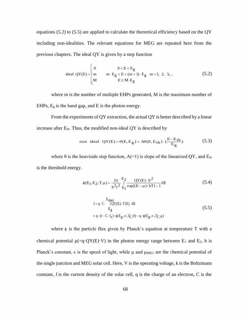
68
equations (5.2) to (5.5) are applied to calculate the theoretical efficiency based on the QY
including non-idealities. The relevant equations for MEG are repeated here from the
previous chapters. The ideal QY is given by a step function
,...3,2,1m
gEMEM
gE)1m(EgEmm
gEE00
)E(QYideal
(5.2)
where m is the number of multiple EHPs generated, M is the maximum number of
EHPs, Eg is the band gap, and E is the photon energy.
From the experiments of QY extraction, the actual QY is better described by a linear
increase after Eth. Thus, the modified non-ideal QY is described by
)
gEthEE
()thE,E(A)gE,E()E(QYidealnon
(5.3)
where θ is the heaviside step function, A(=1) is slope of the linearized QY, and Eth
is the threshold energy.
2E
1E
dE1]kT/)Eexp[(
2E)E(QY
2c3h
2),T,2E,1E(
(5.4)
),CT,,gE(q)0,CT,,gE()sfC1(q
maxE
gE
dE)E()E(QYCqJ
(5.5)
where is the particle flux given by Planck’s equation at temperature T with a
chemical potential µ(=q·QY(E)·V) in the photon energy range between E1 and E2, h is
Planck’s constant, c is the speed of light, while μ and μMEG are the chemical potential of
the single junction and MEG solar cell. Here, V is the operating voltage, k is the Boltzmann
constant, J is the current density of the solar cell, q is the charge of an electron, C is the

69
optical concentration, fS is the geometry factor (=1/46200), Eg is the bandgap energy, TC is
the solar cell’s temperature (=300K), Emax (=4.428 eV at 280 nm wavelength) is the highest
photon energy of the terrestrial spectrum, and Г(E) is the converted terrestrial spectrum
from ASTMG 173-03.
Fig. 5.2. The QY and photon energy of silicon QD, The maximum value of ideal QY is 3
and changes the delayed Eth as 2Eg, 3Eg and 4Eg. (a) Eg=1.12eV, (b) Eg=1.2 eV,
(c)Eg=1.3 eV and (d)Eg=1.4 eV © [2013 IEEE] [86].
Fig.5.2 describes the ideal and non-ideal QY of silicon as a function of the effective
bandgap and threshold energy. Under ideal QY conditions, even though the QY can
increase infinitely, the solar photon flux at high photon energies is negligible so that QY is
limited to two or three (M≤3). On the contrary, the non-ideal maximum QY depends on
the threshold energy and reduces with increasing Eth. Thus, with increasing effective

70
bandgap of the silicon QDs, the maximum non-ideal QY is decreased. And, Table 5.2
summarizes the simulation results based on Fig. 5.2 in section 5.3.1.
5.2.4 MJMEG Solar Cells with silicon QDs
The efficiency of MEG solar cells with silicon nanostructures is limited by the
maximum ideal QY (=3 or 300%) under terrestrial spectrum conditions. A more efficient
way to overcome thermalization losses is utilizing multijunction solar cells with
concentrators resulting in increased photo-generated current of each cell.
For the MJMEGSCs, one has to consider the relationship between QY and spectral
splitting to achieve non-overlapping QY and to maximize the MEG effect of each layer of
the MJMEGSCs.
The basic assumption of MJMEGSCs is that every layer has carrier multiplication
or MEG [60]. However, the net MEG effect of each layer depends on the QY interacting
with spectral splitting. For instance, the top junction of a 2J MJMEGSC shows relatively
high QY because there is no blocking layer to absorb the high energy photons [60].
The maximum QY of the bottom junction is limited. Fig. 5.3 describes how the
maximum QY depends on the bandgaps of each junction within 2J MJMEGSCs.
First, it presumes that bulk silicon or silicon QDs are used for the top junction
material to obtain the appropriate maximum carrier multiplications. Then, choosing
possible materials for the bottom junction can be flexible to have the maximum QY. The
effective bandgap of Si for the top junction is determined by the size of the QDs or
nanostructures. The simulations determine the optimum bandgaps and corresponding QYs
under both ideal and non-ideal QY conditions. Fig.5.3 (a) and (c) show QY vs. photon
energy for the optimum bandgaps derived from the ideal QY with and without

71
concentration. Also plotted in (a) and (c) are the corresponding non-ideal QYs for these
same bandgap materials. Fig.5.3 (b) and (d) show QY vs. photon energy for the optimum
bandgaps derived using the non-ideal QYs with and without concentration and again also
displays the ideal QYs for comparison. These results are discussed in more detail in section
5.3.2. It is obvious from Fig.5.3 that the more step-like ideal QY will increase the photo-
generated current and theoretical efficiencies compared to the non-ideal QY.
Fig. 5.3. The spectral splitting of double junction-MJMEG solar cells. The maximum QY
depends on its bandgaps of each junction (a) and (b) are under one sun
illumination, (c) and (d) are under full concentration (C=46200).
© [2013 IEEE] [86].
5.3 Results and discussion
5.3.1 Silicon MEG solar cell
Using the QYs in Fig.5.2, the author obtains the maximum theoretical conversion
efficiency under one sun illumination for fixed M=3 and varying threshold energies for
four different effective bandgap materials, with the results shown in Table 5.2.

72
Table 5.2. The efficiency of Si MEG ideal QY and non-ideal QY under one sun (ASTMG
173-03) where is M is the maximum QY and value of Eth is for M=3 © [2013
IEEE] [86].
1.12 eV 1.2 eV 1.3 eV 1.4 eV
M=3 41.8 40.0 37.9 36.6
Eth 1.12 eV 1.2 eV 1.3 eV 1.4 eV
2Eg 36.6 35.6 34.4 34.2
3Eg 33.5 33.3 33.1 33.3
4Eg 33.3 33.3 33.1 33.1
For the ideal QY (M=3, Eg=1.2 eV), the theoretical efficiency of the ideal and non-
ideal QY cases give quite different results. For the ideal QY (M=3, Eg=1.2 eV), the
theoretical efficiency of a Si MEG is over 40.0%, decreasing with increasing effective
bandgap. For the non-ideal QY, the maximum conversion efficiency is strongly dependent
on both effective bandgap and threshold energies. Table 5.2 shows that the non-ideal QY
drops the efficiency from 41.8% (ideal QY) to 36.6% when Eg = 1.12 eV, with a smaller
drop for higher effective band gaps. For instance, if the effective bandgap of silicon is 1.4
eV based on a 6.5 nm diameter QD (Table 5.1), its theoretical efficiency with non-ideal
QY and its corresponding maximum QY are (1) 34.2% and 2.17 (Eth=2Eg), (2) 33.3% and
1.16 (Eth=3Eg) and (3) 33.1% and 1(Eth=4Eg). Thus, as shown in Table 5.3, the cell
efficiency only improves if Eth is near 2Eg. If Eth is increased, the beneficial effects of
MEG are greatly reduced. For Eg,effective=1.12 eV, the efficiency above Eth = 3Eg essentially
saturates, and the difference between Eth = 3Eg and Eth = 4Eg is 0.2% absolute regardless
of the value of the bandgap. Further, at these threshold energy ranges, the efficiency gains

73
from the MEG process are relatively small compared to an ideal device without the MEG
processes.
As shown in Fig. 5.1 and Table 5.1, the size of the QDs determines their effective
bandgaps. With increasing Si QD size, the effective bandgap approaches the bulk-bandgap.
Based on the detailed balance calculations presented here, the best performance for Si QDs
is approached by making the QDs as large as possible while simultaneously preserving the
beneficial effects of confinement in terms of lack of momentum conservation and hence an
ideal threshold energy approaching energy approaching 2Eg. Thus for subsequent
simulations the author has selected an effective bandgap of 1.2 eV to maximize the effect
of MEG.
Further, there are several ways to increase efficiency of MEG solar cells. One way
is using concentration which enhances the conversion efficiency of solar cells by increasing
both the light-generated current and the quasi-Fermi level separation. Another is realizing
a more step-like QY vs. photon energy behavior. The current QY measurements in silicon
show this possibility, that the shape of the QY is important in enhancing MEG solar cell
performance by producing more light-generated current [91].
For this simulation, the author selects three maximum ideal QYs (M=1, 2, and 3)
and one non-ideal QY with Eth=2Eg and an effective Eg=1.2 eV to calculate theoretical cell
efficiencies for a variety of concentration levels. The results are shown in Fig.5.4 and
Table 5.3. For the ideal QY case, After M=2 the theoretical efficiencies vs. concentration
are saturated since there is no further reduction of the thermalization loss. Therefore, in
case of silicon nanostructures, 200% to 300% maximum QY is the critical point to optimize
silicon nanostructured MEG solar cells.

74
Table 5.3. The efficiency of Si MEG with ideal QY and non-ideal QY with changing
concentration where C is concentration. (Effective Eg=1.2 eV)
Si C=1 C=100 C=1000 C=10000 C=46200
M=1 33.4 37.7 40.0 42.3 43.8
M=2 39.8 44.2 46.8 49.4 51.0
M=3 40.0 44.3 47.0 49.6 51.1
Eth=2Eg @M=3 35.6 39.7 42.1 44.6 46.2
Fig. 5.4. The Efficiency VS Concentration of Si (Eg=1.2 eV) MEG under terrestrial
spectrum with concentration. The concentration axis presents as log scale
where M is the maximum QY © [2013 IEEE] [86].
As expected, the non-ideal QY results in cell efficiencies consistently below the
ideal QY and its maximum conversion efficiency under full concentration is 46.2%. In a
realistic concentration like 100 or 1000 suns, the expected efficiencies are 39.8% and 42.2%
respectively.

75
5.3.2 MJMEG hybrid solar cells with Si QDs
In the previous section, MEG solar cells were analyzed theoretically and it was
shown that when including either ideal or non-ideal QY, the calculated efficiency under
one sun is not greatly improved. Therefore, the author has proposed double junction
MJMEG hybrid solar cells as a better approach and has proceeded to determine their
detailed balance efficiency limits.
The double junction MJMEG cell is assumed to have a top junction composed of
silicon QDs for which the effective bandgap depends on QD size. The bandgap of silicon
relative to the solar spectrum dictates that it should be used at the top junction in order to
absorb photons that can effectively generate carrier multiplication. The simulations point
out the significance of MEG effects within the bottom junction for maximizing QY. To
maximize carrier multiplication, the optimum material for the bottom junction should have
a small bandgap and a threshold energy close to two times the bandgap to prevent non-
overlapping QY and match the solar spectra.
The ideal QY can always satisfy this condition due to its step-like nature. However,
the optimum bandgaps calculated using the non-ideal QY are quite different because, in
the non-ideal QY case, the maximum QY of the bottom junction is determined by the
bandgap of the top junction. Thus, if the threshold energy of bottom junction is close to the
top junction bandgap, the maximum QY is approximately 1 and the bottom junction will
behave like a conventional multijunction solar cell. In order for the bottom junction to show
a clear MEG effect the measured QY should approximate the ideal QY to maximize carrier
multiplication.

76
Table 5.4. The double junction of MJMEG solar cells using Si QDs for upper junction
where S is the series connection. H stands for MJMEG Hybrid solar cells. IQY
is the ideal QY and NQY is the non-ideal QY © [2013 IEEE] [86]
C=1 Eg1(eV) Eg2(eV) η (%)
2J
(S,C)
0.5 1.12
(Si Bulk)
23.3
2J
(S,C)
0.75 1.52 44.2
2J
(S,H,IQY)
0.57
(InAs)
1.38
(Si QD, 6.9nm)
47.8 Fig 5.3 (a)
2J
(S,H,NQY)
0.57
(InAs)
1.38
(Si QD, 6.9nm)
40.9 Fig 5.3 (a)
2J
(S,H,IQY)
0.73
(Ge, InN)
1.51
(Si QD, 5.1 nm)
46.9 Fig 5.3 (b)
2J
(S,H,NQY)
0.73
(Ge, InN)
1.51
(Si QD, 5.1 nm)
44.6 Fig 5.3 (b)
C=46200 Eg1(eV) Eg2(eV), η (%)
2J
(S,C)
0.5 1.12
(Si Bulk)
37.9
2J
(S,C)
0.7
(Ge)
1.44
(GaAs)
60.4
2J
(S,H,IQY)
0.31
(,InAs)
1.12
(Si Bulk)
69.4 Fig 5.3 (c)
2J
(S,H,NQY)
0.31
(InAs)
1.12
(Si Bulk)
58.1 Fig 5.3 (c)
2J
(S,H,IQY)
0.7
(Ge, InN)
1.44
(Si QD, 5.9nm)
63.8 Fig 5.3 (d)
2J
(S,H,NQY)
0.7
(Ge, InN)
1.44
(Si QD, 5.9nm)
61.0 Fig 5.3 (d)
From Table 5.4, the optimum bandgaps calculated using the non-ideal QY are
nearly the same as the conventional double junction MJ solar cells and show only slightly
increased efficiencies. Therefore, the QY for MJMEG solar cells has to be similar to the
ideal QY to maximize the MJMEG solar cells. For instance, the theoretical efficiency using
the ideal QY for Eg1=0.58 eV and Eg2=1.38 eV is 47.8% under one sun and its efficiency
is 6.9% higher than non-ideal QY. The simulated efficiency using the non-ideal QY for

77
Eg1=0.73 eV and Eg2=1.51 eV is 44.6%, whereas the calculated efficiency based on the
ideal QY with same bandgaps is 46.9%.
Choosing the appropriate materials for silicon based double junction MJMEGs is
important. There are various reports of QY extraction experiments for group II-VI, III-V
and IV materials such as PbSe [29], PbS [29], InN [84] and InAs [43] and Ge [35] using
ultra-fast transient absorption methods, observing impact ionization, and through
simulations. Publications describe materials compatible with silicon nanostructures
including Si on Ge, III-V nanostructures on silicon substrates and silicon hybrid solar cells
[92]-[94].For instance, Ge (for the bottom junction) and Si QDs (for the top junction) can
be a good approache. InAs or InN nanostructures on Si substrate have been mentioned for
variety of applications for optoelectronic devices due to strain accommodation at the
nanostructure surfaces [35],[92]. Finally, all-Si QD layers can tune light-absorption paths
[95]. But, the all-Si QD method suffers from the relatively high bandgap of silicon (Eg=1.12
eV, Eth=2.24 eV) in the bottom junction preventing MEG and thus these cells display the
nearly same theoretical efficiency as conventional multijunction solar cells from detailed
balance calculations. For instance, the conversion efficiencies are 49.3% for MJ and 49.4%
for MJMEG where Eg1=1.12 eV, Eg2=1.5 eV and Eg3=2.0 eV with one sun under terrestrial
spectrum.
Therefore, the most promising way to realize MJMEGSC with silicon
nanostructures is the combination with Ge or III-V materials. However, the lattice
mismatches between Si and these other materials need to be overcome for optimum
current-matched multijunction solar cells.
78
5.4 Conclusion
In summary, the author has investigated the effect of the threshold energy of Si
multiple exciton generation solar cells on conversion efficiency through detailed balance
calculations including quantum size effects. In general, a smaller threshold energy and
ideal step like QY are important in realizing conversion efficiencies greater than the one
junction limit. Quantum dots have a size–dependent effective bandgap. Thus, controlling
both QD size for its effective bandgap and threshold energy is very important in
maximizing the efficiency of MEG based solar cells, which the author demonstrates
through the MEG detailed balance calculations for varying Si QD diameters reported here.
MJMEG is an alternative way to effectively manage the thermalization losses of hot
carriers. The author has shown how the behavior of the QY of each junction is critical to
maximize the effects of MEG and explained why silicon nanostructures for the top junction
are ideal due to its maximum QY. The simulations identify a number of possible materials
such as Ge, InN and InAs as suitable bottom junction materials.

79
CHAPTER 6
THE EXPERIMENTS OF SILICON NANOSTRUCTURE SOLAR CELLS
6.1 Introduction
Nanostructured solar cells utilizing quantum confinement effects to boost
conversion efficiency are an attractive option to replace the current solar cell technology.
Such nanostructure based cells are called "third generation" solar cells and development
efforts so far are largely confined to research laboratories.
For last half-century, crystalline silicon solar cells have been at the forefront of the
PV industry as a result of the success of commercial and academic research. Crystalline
silicon solar cells in the laboratory reached 24.7% conversion efficiency in 1999 [8], and
currently, commercial crystalline silicon PV devices show an average 20% conversion
efficiency [96],[97]. PV devices with this range of efficiency are called first generation PV
devices. The first generation solar cell is based on silicon wafers with texturing for light
trapping and screen-printing to make ohmic-contacts [96],[98].
In these first generation PV cells, to obtain high conversion efficiencies, it is
necessary to control the surface morphology to reduce the reflectance and improve the
electrical performance. Typically, in third generation devices like multiple exciton
generation solar cells, it is also significant to consider how to integrate it with appropriate
nanostructures for obtaining good quantum confinements that MEG and increasing light-
generated current.
In today's manufacturing of silicon solar cells much effort is focused on the
processes to texture the silicon surface, the subsequent cleaning of that surface, and the

80
deposition of a silicon nitride film [99]. MEG solar cells also have to focus on these issues
to improve the entire properties even if there are carrier multiplications. Therefore,
optimizing and controlling these processes is challenging since the final electrical
performance depends on both the material qualities and fabrication methods. Certainly, it
increases the cost of silicon PV modules due to additional purifications of the surface of
the silicon wafers [96]-[98].
Recently, silicon heterojunction with intrinsic thin-layer (HIT) solar cells have
appeared as novel structures with high conversion efficiencies (24.7% and 25.6%)
[10],[100]. Intrinsic amorphous silicon (α-Si) shows good passivation characteristics on a
clean single crystal silicon surface and these cells achieve high open circuit voltages [101].
However, HIT cells still require texturing and cleaning of the single crystal silicon surface
and their performance is very sensitive to the nature of that surface upon which the α-Si is
deposited.
By depositing amorphous silicon at the silicon nanostructured solar cells, the author
will discuss the effects of this approach for the future silicon PV cells.
In this chapter, it will describe the fabrication and measurements of both optical
and electrical properties of a future generation silicon nano PV cells. This experiment is an
initial attempt at fabricating silicon nanostructured solar cells with electron-beam
lithography (EBL) and future work aimed at MEG solar cells. This project was a joint
effort with Mr. Green as part of the 2013 National Nanotechnology Infrastructure Network
Research Experience for Undergraduates program [Christopher Green, NNIN REU, 2013]
[102].(see Appendix. D)

81
6.2 Silicon Nanostructured Solar Cells
Silicon nanostructured solar cells are recently developed PV cells using quantum
dots or nanowires [97],[103],[104] to increase the effective conversion efficiency and to
absorb light effectively. The effect of nanostructures is to make it possible to change the
material properties such that indirect bandgap materials can behave like direct bandgap
materials due to discrete energy levels inside quantum structures [105]. The effective
bandgap is influenced by the size of nanostructures; i.e., the effective bandgap is inversely
proportional to the size of nanostructures. Typical nanostructures have sub-100nm
dimensions, much less than the wavelength of the light illuminating the solar cell making
the shape, density, and composition of the nanostructures all factors in determining the
optical absorption properties The management of these sub-wavelength dimensions can
give a great impact for optimizing reflectance and these structures have unique features of
separation of light absorption and carrier transport in the confinement of electrons in the
quantum structures.
In general, MEG solar cells have to minimize the optical losses with modifications
of processes including both passivation and anti-reflection coating for better quantum yield.
In this project, the author focused on electron-beam defined front surface nanostructures
only, passivated with a thin deposited amorphous silicon film and with no additional anti-
reflection coating. The second benefit of a silicon nanostructured solar cell is the possibility
to generate more than one electron and hole pair per one incoming photon by impact
ionization, increasing the short circuit current. Even though the quantum yield extractions
of nanostructures have proven the quantum yield can be over 100%, experiments do not
show a great improvement of conversion efficiency likely due to surface effects and the

82
use of low bandgap materials [52]. In other words, the MEG phenomenon is still
controversial due to various different results of quantum yield extraction experiment by
ultra-fast time resolved photo-luminescence.
Even if the short current is increased, to date nanostructured solar cells exhibit low
conversion efficiencies with low fill factors and small open circuit voltages and it is clear
much more research is needed to solve these issues [97]. These characteristics will be
discussed in section 6.4.
This work focuses on the fabrication and measurement of both optical and electrical
properties of a silicon nanostructured solar cell with an array of vertical nanopillars
patterned on the front surface of the silicon chosen as the type of nanostructure to be studied.
Using electron beam lithography, the size and pitch of a masking layer is defined and the
pattern transferred into the silicon substrate using dry etching. Initially, the diameter of the
nanopillars was set at 100nm with 700nm spacing between nanopillars and the etch depth
target was approximately 500nm. The cell has a backside diffused emitter and uses shadow
mask defined metallization. The process is detailed in section 6.3.
6.3 Experimental Procedure
Fig. 6.1 is the process flow of fabricating silicon nanostructured solar cells. These
silicon nanostructure solar cells are fabricated by n+ doped back-side junction of p-type
300 µm thickness of silicon wafers with p-α-Si/i-α-Si and aluminum contacts. The process
flow and hence the later results were constrained by the availability of a tool which was
delayed in getting up and running.
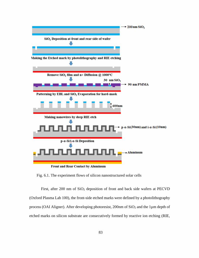
83
Fig. 6.1. The experiment flows of silicon nanostructured solar cells
First, after 200 nm of SiO2 deposition of front and back side wafers at PECVD
(Oxford Plasma Lab 100), the front-side etched marks were defined by a photolithography
process (OAI Aligner). After developing photoresist, 200nm of SiO2 and the 1µm depth of
etched marks on silicon substrate are consecutively formed by reactive ion etching (RIE,

84
Oxford Instrument Plasmalab 80+). These marks are used for next processes of Aligners
and electron beam lithography (EBL).
Then, the both side of SiO2 layers are removed by Buffered Oxide Etchant about
10 min to completely eliminate the remaining oxide film on the silicon wafers. And, to
make a diffusion mask, the front side of silicon wafer was coated by SiO2 by PECVD
(Oxford Plasma Lab 100) again.
The next step is n+ diffusion for back-side of wafers at 1000°C for one hour and
annealed about 7 hours to make a junction in the rear side of wafers. This process is
supported by the diffusion furnace of ‘Center for Solid State Electronics Research (CSSER)
90nm thickness of PMMA was coated on the front-side of wafers for EBL process.
100nm diameter openings are patterned by EBL equipment (JEOL 6000F/S) in CSSER.
The distance between of nanostructures is about 700nm and the entire die size is small at
1mm × 1mm due to write time limitations. Then, 30nm thickness of SiO2 is deposited with
electron beam evaporation (LESKER #3 at CSSER) followed by liftoff of the PMMA to
make oxide hard masks for the silicon etching.
The nanostructures or nanowires are etched by a Surface Technology Systems
inductively coupled plasma (STS ICP) system using the SiO2 hard masks. Highly
anisotropic nanowires with 600nm height were formed using the Bosch process, which
consists of alternating cycles of etchant using sulfur hexafluoride (SF6) and polymer
deposition from octaflourocyclobutane (C4F8). This method inherently creates scalloping
on the sides of the nanowires. This nanostructures are displayed in Fig. 6.2.
A passivation and contact layer consisting of 10nm intrinsic i-α-Si and 30nm of p-
α-Si was deposited on silicon nanostructures using PECVD (P-5000, Solar Power

85
Laboratory). The effective diameter of silicon nanostructures is increased to 180nm due to
the deposition of these amorphous silicon films.
Fig. 6.2. The fabrication of silicon nanostructures where (a) is the SEM image for
deposition of 30nm thickness SiO2 (b) is the image for silicon nanostructures
after deep RIE etching [Christopher Green, NNIN REU, 2013] [102].
An electron beam evaporation tool, LESKER III at CSSER, was used to deposit
200nm of aluminum (Al) on the front and back sides of the wafer. A shadow mask was
aligned on the front side of the wafer during deposition to prevent the base contact metal
from covering the nanowires.
While measuring the electrical properties of this solar cell, non-alloyed Al contact
on p-type amorphous silicon layer could not give data. Therefore, the wafers were placed
in an oven to allow Al to diffuse through the passivation layer without compromising the
amorphous nature of the layer.

86
6.4 Results
Both the optical reflectance and electrical performance under illumination were
measured for the nanostructured cells and comparisons made to control devices processed
without nanostructures fabricated on the same substrate. Even though this experiment
results cannot provide good information for MEG solar cells, the light-generated current is
increased due to properties of nanostructured solar cells and it will have more
supplementary works to study of nano-PV cells for MEG.
6.4.1 The Electrical Characteristics
Electrical measurements were made on a probe station with illumination provided
by a halogen lamp approximately calibrated to provide AM1.5 illumination. Only the small
nanostructured region of the cell (1mm×1mm) is illuminated since the surrounding region
is masked by the thick base contact aluminum metal, but the cell electrical area is
considerably larger, with obvious negative effects on Voc. The control cell is identically
processed, except no nanowires are etched in the illuminated region. Fig. 6.3 and Table
6.1 are the summary of results.
Table 6.1. The electrical characterization results of silicon-nanostructured solar cells
[Christopher Green, NNIN REU, 2013] [102].
JSC (mA/cm2) VOC (V) FF (%) η (%)
Silicon Nano
PV Cell
21.6 0.44 67.7 6.43
Control
Device
14.1 0.42 55.5 3.48

87
Fig. 6.3. The electrical properties of silicon nanostructured solar cell
[Christopher Green, NNIN REU, 2013] [102].
The current-voltage relationships in Fig. 6.2 also show a series-resistance issue
from the and low fill factor for both the nano and control cell, which is thought to be due
to the lateral resistance between the illuminated area and the front-metal contact. The p-
type and intrinsic amorphous silicon passivation layers have very high sheet resistance and
typically in the HIT solar cell indium tin oxide (ITO) is deposited on these amorphous
silicon layers to reduce the series resistance, something which was not done for these
devices. It is also possible that there is an aluminum to p-a-Si high contact resistance
problem.
The performance could be further improved through optimization of the passivation
technology. The etched nanostructures not only increase the surface area but are also likely
to suffer from surface damage induced by plasma etching, both of which lead to rapid

88
surface recombination. As long minority lifetime is needed which requires minimizing all
recombination sites and thus one needs to find optimum etch conditions to minimize the
surface damage and establish post etch cleans that enable the deposited amorphous silicon
films to effectively passivate the surfaces of the nanostructures.
The experimental results of silicon nanostructures have several drawbacks due to
low open circuit voltage and its low fill factor. Actual diffusion process has conducted at
entire rear side of wafers that even though the size of silicon nanostructures area is 1 mm
× 1 mm, the entire diode size is 10 mm × 10 mm so that the current from nanostructures to
the junction is laterally flowed instead of vertical flowing. Generally, an open circuit
voltage of this solar cell is defined in equation (6.1)
)1OJ
SCJln(
q
TkOCV
(6.1)
Where VOC is an open circuit voltage, k is the Boltzmann constant, T is an solar cell
temperature (=300 K), q is the element of charge, JSC is the short circuit current and J0 is a
recombination current
And, JSC is a factor from light generation under 1 mm × 1mm of nanostructure area
and J0 is a recombination current which depends on diode area (=10 mm × 10 mm ) of solar
cell. Therefore, an asymmetric dimension of solar cell area destroys the entire open circuit
voltage.
To resolve this issue, the n+ diffusion should be localized to prevent the lateral flow
of current. Thus, even though the actual size of diode is 10 mm × 10 mm, in this dissertation,
the experimental results have conducted with an assumption of 1 mm × 1mm area under
light illumination where it is shown in Fig 6.4.

89
Fig. 6.4. The cross-section and top-view of silicon nanostructured solar cells.
Furthermore, to make better silicon nanostructured PV cells, the front side of
nanostructured area and the rear side of should be same. Or, the front-contact with p-α-Si
has to remove and should replace to the all rear contact or should deposit ITO for making
contact with Al. And, it is also necessary to localize diffusion to directly collect the
generated carriers from nanostructures. Thus, the current can flow vertically from
nanostructures to the junction of backside wafers.
6.4.2 The Optical Characteristics
Reflectance measurements were taken of silicon nanostructured patterns using the
Filmetrics F40 microscope with conventionally textured silicon and bare silicon as a
references. The results in Fig. 6.5 plot the reflectance vs. wavelength from 400 to 850 nm.
The reflection characteristics of a conventionally textured silicon solar cell are
better than the silicon nano PV cell and a polished silicon surface. The Si nanowire PV
cells show an optical resonance from 685nm to 750nm wavelength due to the periodic
nanostructures and its minimum reflectance (=2.5%) is lower than the textured silicon solar

90
cell. Other regions show higher reflectance which is not unexpected due to the wide spacing
of the periodic structures of silicon nanostructures. In other words, the high-reflection
region represents bulk-silicon area and the optical resonance region is the nanostructured
area having high-absorption.
Fig. 6.5. The measurements of reflectance between silicon nanostructures PV cell and
textured Si PV and Bulk or bare silicon solar cells [Christopher Green, NNIN
REU, 2013] [102].
6.5 Conclusion
Initial experiments fabricating silicon nanostructured solar cells have been
conducted. These nanostructured solar cells are fabricated by EBL and deep RIE process
with thin amorphous silicon layers for passivation. To investigate light-trapping, the
efficiency has measured under AM1.5 spectrum and shown that the short-circuit current of
silicon nanostructured solar cell is higher than the reference cell. However, its open-circuit
voltage is low due to a large parasitic diode area and the possibly the quality of the surface
passivation. Furthermore, the optical reflectivity has been measured comparing polished

91
silicon, a textured silicon solar cell and the nanostructured solar cell. One significant point
is that the silicon nanostructured solar cell has an optical resonance at 700 nm where its
reflection is lower than the textured solar cell, presumably due to the periodic nature of the
nanowire array.
Further research is needed to optimize the fabrication process increasing the
number of silicon nanostructures to provide higher absorption and enhance the conversion
efficiency for future MEG solar cells. And, studying the physical parameters such as
diameter, spacing, and structure on absorbance must be performed to allow for
optimization of nanowire structures. Furthermore, a study of passivation would help to
improve both optical and electrical characteristics.
92
CHAPTER 7
LIMITING EFFICIENCIES OF INTERMEDIATE BAND SOLAR CELLS WITH
TANDEM CONFIGURATION
7.1 Introduction
Tandem (or multijunction) solar cells present high experimental conversion
efficiencies over 40%, and have the highest efficiency record [4], [106]. For instance, the
recent champion record of triple junction tandem solar cell is 44.4 percent
(InGaP/GaAs/InGaAs, 302 suns) with using inverted metamorphic structures [6].
Furthermore, the conversion efficiency of a four junction tandem solar cell has approached
to 44.7% [11]. Thus, the experimental world record of tandem solar cell will approach to
near 50%.
However, due to material imperfections in the materials used in tandem solar cell,
it is still necessary to minimize defects by using novel growth technologies [ 107 ].
Appropriate material selections are also important to enhance the properties of tandem
solar cell with acceptable lattice mismatches. Therefore, a key challenge is to find the
appropriate trade-offs between number of junctions, materials which allow low defect
concentration in order to improve the overall efficiency of tandem solar cells.
Intermediate band solar cells (IBSC) have three optical transitions due to the
presence of an intermediate band (IB) by adding another energy level inside the bandgap.
The theoretical conversion efficiency is 63.2% with full concentration which it is similar
to the value of a triple junction tandem solar cell [15], Currently, InAs/GaAs or InAs/GaSb
systems are researched in order to fabricate IBSCs [108] but experimental results show low

93
efficiencies, around 20%, showing there are still challenges and a need for further
improvements in quantum dot systems to make IBSC [109].
Integrating the IBSC concept with a tandem solar cell (IBTSC) shows a large
impact because of the three carriers transitions in an IBSC [ 110]-[113]. Theoretical
conversion efficiencies of double junction (2J) IBTSC can be similar to the calculated
efficiency of 5 or 6 junction tandem solar cells under concentrated sunlight. Thus, 2J
IBTSC provides the large improvement in the theoretical efficiency for the same reduced
number of junctions. The same efficiency as using large number of junctions in
conventional tandem solar cells and be reached in an IBTSC with a smaller number of
junctions.
The spectral splitting between the junctions is the key to determining optimized
physical parameters for each junction to avoid spectrum overlap between layers. One
approach to spectral splitting is to assume that the 6 effective band gaps in the two IBSC
structures can take any value, and that light will automatically find its optimum band gap.
This is used in [110] and [111]. In this work, the requirements on spectral selectivity are
reduced, and it is assumed that the top IBSC contains the top three effective band gaps.
While it is still assumed that within each IBSC spectral selectivity occurs, spectral
selectivity is not assumed between the two IBSC structures. This is implemented by
dividing the incident solar radiation into two regions to clearly define the two bandgaps for
barrier materials, and then each bandgap has properly ordered of three sub-bandgaps: ECI,
EIV, and Eg.
The advantage of 2J IBTSC is that there is increased flexibility in the choice of
optimized materials for the efficient absorption of photon energies and the relaxation of

94
strain due to lattice mismatch. Therefore, the author has searched appropriate materials
from group IV, III-V materials. In addition to the constraints placed on the optimum band
gap, and additional constraint on material selection is introduced by the band offsets, which
give rise to either a Type I or Type II quantum well or QD system. In type I in quantum
dot (QD) structures the electrons and holes are confined in the same quantum well systems.
But, type II structures show an indirect transition of an electron and hole due to spatially
separated with neighbor quantum well or different band alignment. In other words, holes
are localized due to the valence band offset, similarly, electrons will have a potential barrier
at the same location of valence band offset region. Because of different spatial separation
in quantum wells between type I and type II, the wave-function at the conduction band in
type II is not directly correlated with valence band offset.
In this chapter, the authors present detailed balance limit calculations for 2J IBTSCs
under full concentration (= 46200) under blackbody radiation and examined candidate
material combinations. This chapter is based on [113] in which the author has further
discussed about the material selection of IBTSC. (see Appendix. E)
7.2 Theory
7.2.1 Detailed Balance Model of IBTSC
First, the author use the most of assumptions in both tandem and IB solar cells in
[20],[75],[76]. Each junction uses the ideal perfect mirror to avoid spectral overlapping
between neighbor junctions [13].
Due to (1) selectively absorbing photon energy in both IBSC and tandem solar cells
and (2) the similar efficiencies between IBSC and 3J tandem solar cells, it is attractive to

95
integrate both concepts to enhance the characteristics of IBSC by tandem configuration.
General configurations of 2J IBTSC is shown in Fig.7.1 that 6 transitions of carriers should
be spectrally separated.
The detailed balance equations of IBTSC are shown below from equation (7.1) to
(7.6). Equation (7.1) and (7.2) are the generation rate and recombination rate of IBSC
respectively.
Fig. 7.1. The schematic of a tandem double junction IBTSC.
2E
1E
dE1]CkT/Eexp[
2E
2c3h
2)CSf1(
2E
1E
dE1]SUNkT/Eexp[
2E
2c3h
2CSf1E,2EG
(7.1)
2E
1E C
2
231E,2E dE1]kT/)Eexp[(
E
ch
2R
(7.2)

96
where G is generation rate and R is a recombination rate, fS is a geometric factor
(=1/46200) in this case, C is a sun’s concentration (=1~46200), h is a plank constant, c is
speed of light, E1 and E2 are energy states, k is a Boltzmann constant, TSUN is a sun’s
temperature (=6000K) and TC is an ambient temperature (=300K), µ is a chemical potential
(=q·V) where V is an operating voltage.
The current density (J) of the ith junction in the IBTSC is given by
)R-GR-q(G J CI(i)CI(i)CV(i)CV(i)(i) (7.3)
where subscript “i” is the number of junction (i=1,2,3…), subscript CV indicate the
carrier transitions between the valence band (VB) and the conduction band (CB), and
subscript CI indicates the carrier transitions between the IB and the CB.
Assuming no carrier extractions from IB can write in equation (7.4):
IV(i)R-IV(i)G CI(i)R-CI(i)G (7.4)
where subscript IV indicates the carrier transitions between the valence band (VB)
and IB.
The chemical potential of IBTSC is the summation of voltages between (1) the
IB to CB and (2) the VB to IB:
IV(i)CI(i)CV(i) qV qV qV (7.5)
Compared to the conventional tandem solar cell, each stack of the IBTSC has three
different bandgaps which are Eg(i), EIV(i) and ECI(i) as shown in Fig.7.1.

97
Fig. 7.2. The schematic of electrical circuit model of IBSC. It is composed of three diodes
having bandgaps of ECI, EIV and ECV..
Thus, it can show an equivalent electrical circuit model in Fig. 7.2. Two diodes, ECI
and EIV are series-connected and these two diodes are parallel-connected with ECV.
The IBTSC model requires careful accounting of the available photon flux vs.
energy, as this will be quite different from that of the typical tandem cell. To calculate this,
the solar spectrum is divided into two regions. In Fig.7.3 of section 7.2.2, Ehi(1) is defined
as the boundary point dividing the two regions which IBSC1 and IBSC2 are the spectrum
ranges for bottom and top junction of the IBTSC respectively. After selecting Ehi(1), it can
set the proper order of sub-bandgaps can be set for each junction where
ECI1<EIV1<Eg1<ECI2<EIV2<Eg2.
7.2.2 Solar Spectrum Splitting of Double Junction IBTSC
In tandem solar cells, a principle of solar spectrum splitting is that each layer uses
an ideal perfect mirror to absorb appropriate incoming photon energy and other photons

98
reflect the outside mirror [20]. Like tandem solar cells, IBTSC uses three light absorption
paths of incoming photons for each junction including both a bandgap and two sub-photon
energies (ECI and EIV). Further, t also uses an ideal mirror to absorb appropriate energy of
light.
Fig.7.3 describes the solar spectrum splitting for both tandem solar cells and IBTSC.
Conventional tandem, IBSC, and IBTSC cells all achieve improves conversion efficiencies
by selection of optimum bandgaps.
Below Ehi(1), we consider the IBSC as the bottom junction of IBTSC. In other words,
the incident photon flux will reflect above Ehi(1) and the bandgaps of the lower IBSC
(ECI1,EIV1 and Eg1) will have energies below Ehi(1).
Fig.7.3. The spectral splitting of two regions for 2J IBTSC
For instance, if Ehi(1) is 1.5 eV, the upper solar spectrum range can be considered as
top junction IBTSC (=IBSC2) and below 1.5 eV range is for the bottom junction (=IBSC1).

99
The proper values of ECI1, EIV1 and Eg1 will be determined below 1.5 eV based on equation
(7.4). In case of the next junction defined by Ehi(2) as infinity, the proper range of ECI2, EIV2
and Eg2 will be determined between Ehi(1) and Ehi(2). The minimum value of ECI2 should be
the same or higher than Ehi(1) to avoid spectrum overlapping and maintain enough margin
to extract carriers from the bottom junctions. If ECI2 is below Ehi(1), there will be a range of
spectrum overlapping between ECI2 and Eg1. Also, if Ehi(1) is not properly chosen such that
the difference between Ehi(1) and Eg1 can be small, the photo-current component for carrier
extraction from VB to CB of bottom junction will be small or negligible. In other words,
the dominant contribution is from the IB to CB so the entire effect of bottom junction in
the IBTSC will operate as a two-junction series-connected tandem solar cell composed of
ECI1 and EIV1. Explicit separation of the solar spectrum is significant while designing
multiple layers of IBTSC.
7.3 Results
After regarding all suggested parameters for simulations, the author present results
of 2J IBTSC’s theoretical conversion efficiencies and its optimum bandgaps under full
concentration (=46200 suns). The results are compared with six junction tandem solar cells
under full concentration. All collected data are displayed in (1) Fig.7.4 and Table 7.1 for
double junction IBTSC and (2) Table 7.2 for six junction tandem solar cells.
7.3.1 The thermodynamic Limits of double junction IBTSCs
The maximum theoretical conversion efficiencies under full concentration in the
series-connected IBTSC is 0.7% less than 6 junction tandem solar cells. Ehi(1) is 1.19 eV
and Eg1 is 0.32 eV below Ehi(1). The difference between Ehi(1) and Eg1 is important in

100
determining the properties of the lower ICSC. If the difference between the two is small,
then the number of photons in this energy range is also small, and hence the current is also
small.
Fig.7.4. Efficiency vs. Ehi(1) for double junction with an independent connection (red line)
and a series-connection (blue line) under full concentration (J.Lee, [113],2012).
Table 7.1. The optimum bandgaps and maximum efficiency (η) of independent (I) and
series (S) connected double junction IBTSCs under blackbody radiation with full
concentration [J.Lee, [113],2012].
Conc ECI1
(eV)
EIV1
(eV)
Eg1
(eV)
ECI2
(eV)
EIV2
(eV)
Eg2
(eV)
η
(%)
46200 I 0.36 0.75 1.11 1.50 2.06 3.56 73.2
S 0.21 0.66 0.87 1.19 1.75 2.94 72.7

101
Table 7.2. The optimum bandgaps and maximum efficiency (η) of six junction tandem solar
cell under blackbody radiation where concentration (=Conc) is 46200 sun. [J.Lee,
[113],2012].
Conc Eg1
(eV)
Eg2
(eV)
Eg3
(eV)
Eg4
(eV)
Eg5
(eV)
Eg6
(eV)
η
(%)
46200 I 0.40 0.78 1.16 1.59 2.11 2.86 74.4
S 0.37 0.70 1.00 1.32 1.71 2.30 73.4
These results presume that the dominant carrier transition in the bottom junction
IBTSC is from IB to CB and it is negligible from VB to CB.
The maximum theoretical efficiency (=73.2%) of independent-connected 2J IBTSC
under full concentration is similar to a series-connected six junction tandem solar cells
(=73.4%) as shown in from Table 7.1 and Table 7.2.
The material choices for independent connection can be also wide due to large
bandgaps to compose QDs. Note that the bottom junction of the series-connected IBTSC
requires a lower bandgap, an issue due to limited choices of low bandgap materials suitable
for QD formation.
Next, the author discusses the material combinations for 2J IBTSC with the
combination between independent and series-connections.
For concentrated sunlight, the results of 2J series-connected IBTSC are shown in
Table 7.1. It shows that barrier materials near 0.9 eV are an appropriate choice for
monolithic growth with GaN combination for 2J IBTSC. But, in the low bandgap materials
with super lattice structure, hot carriers can easily escape at CB of bottom junction that can
reduce the electrical properties of 2J IBTSC due to low carrier extraction margin from Eg1

102
to Ehi(1), small confined states in QDs and dependence of temperature. Therefore, the light-
generated currents are small not preserving the operating voltage of bottom junction IBTSC.
Eg
EIV
ECI
IB
IBSCN Emitter IB RegionP Emitter
(b) Type II(a) Type I
Carrier Transition from VB to CB
Carrier Transition from VB to IB
Carrier Transition from IB to CB
Intermediate Band
Eg
EIV
ECI
IB
IBSCN Emitter IB RegionP Emitter
CB
VB
CB
VB
Fig.7.5. Two types of band structures for a double junction IBTSC where (a) is type I
and (b) is the type II.
Type I or type II structures for IBTSC is displayed in Fig 7.5. The general IBSC
band structure is type I structure. However, type I has drawbacks such as reducing photo-
current due to different transition rates between (1) VB to IB and (2) IB to CB and
decreasing open-circuit voltage because of VB offset due to localized bound states at VB
[114].

103
Therefore, the type II is an alternative due to increasing both carrier life time and
photo-current compared to type I structure. But, due to overlapping of wave-functions, the
different absorption coefficient should regard between type I and type II.
7.3.2 Material Selection for IBTSC
Fig 7.4 and Table 7.1 show several ways to from 2J IBTSC such as (1) Si/Ge, III-
V for bottom most junction and GaN related materials or wide-bandgap of II-VI for top
junction of independent connection (IC) and (2) low bandgap III-V (for bottom junction)
and high bandgap of III-V or II-VI (for top junction) for a series connection (SC).
III-V combinations are well-established approaches to compose IBSC. As well, II-
VI material combinations are also good choices for top junction materials for broad choices.
In case of IC, an optimum bandgap of bottom junction is 1.11 eV which it is similar
to Si, InGaAs, AlGaSb and GaAsSb. The author does not discuss the composition of mole
fraction for optimum band gaps, since such calculations require assumptions about specific
device parameters such as strain. Possible combinations are Si/Ge [115], InGaAs/InAs
[116], AlGaSb/InSb [117] and GaAsSb/InAs [118] under the concentrated sunlight. In the
top junction of IC, GaN/InGaN [119],[120] and AlGaN/InGaN [121] are good choices.
And, II-VI compound semiconductor can give broad materials choices. For instance, ZnS
(=3.7 V) [122] is wide bandgap materials and incorporating with Cr to make deep impurity
levels photovoltaic devices.
For a 2J IBTSC, the optimum materials have several choices. First, the barrier
material for bottom junction is near 0.9eV materials under concentration range. Possible
combinations are InGaAs/InAs quantum dot or quantum well systems.

104
For the top junction materials, it should be matched with near 3 eV so that (1) III-
Nitride and (2) II-VI ZnMgSe, ZnSSe [123] and ZnCdS with transition metal or hetero-
structures are appropriate choices with considering of lattice mismatches.
7.4 Conclusion
A detailed balance of double junction IBTSCs has been developed to show the
advantages of minimizing the number of junctions and to search for appropriate material
combinations. The characteristics of two-junction hybrid IBTSC are similar to a theoretical
conversion efficiency of six-junction conventional tandem solar cells. Because of the
transition of three carriers, a single IBSC can show the properties of triple junction tandem
solar cells. The author has discussed the material selections of 2J IBTSC with results of
independent-connected and series-connected solar cells. In an independent connection of
2J IBTSC, the material combinations are Si/Ge for bottom junction and GaN/InGaN for
top junction. But, in case of series-connection, materials for the bottom junction show 0.9
eV which it should be composed of low bandgap materials. And, due to 3 eV wide-bandgap
barrier materials of top junction, there are various options to choose materials such as III-
V Nitride and II-VI combinations.

105
CHAPTER 8
THE THERMODYNAMIC LIMIT OF INTERMEDIATE BAND SOLAR CELLS
ASSISTED WITH MULTIPLE EXCITON GENERATION
8.1 Introduction
Intermediate band solar cells (IBSC) with quantum dots (QD) are a promising
concept among third generation photovoltaic devices aimed for overcoming the single
junction efficiency limit [12],[15]. By inserting another energy level inside the bandgap
and assuming strong absorption of light through sub-paths, three carrier transitions are
possible: (1) valence band (VB) to conduction band (VB), (2) VB to intermediate band (IB)
and (3) IB to CB [15]. In equilibrium, the IB level occupancy is balanced by two transitions
which are from VB to IB and from IB to CB [15]. The additional generated carriers in the
CB contribute to the electrical current and the IBSC achieves a maximum theoretical
efficiency of 63.2% due to absorption of photons with energy less than the bandgap [15].
After the IBSC concept was initially reported [15], subsequent research focused on
(1) further developments of detailed balance theory of the IBSC [124],[125] and (2)
possible candidate materials to build IBSC based on ab-initio calculations and bandgap
engineering. Experiments have been conducted to make IBSC using III-V compound
semiconductor materials such as GaAs/InAs or ternary material systems such as GaNAs
and other combinations [126]-[131]. These experimental results demonstrate near or less
than 20% efficiency cells [16],[132]-[135]. Recent experimental IBSC research proves the
existence of two photon carrier generation by photoluminescence or electroluminescence
[136],[137].

106
Theoretically, more advanced IBSC concepts have been proposed including both
Auger generation at the IB and multiband cells with IBSC [138]-[144].
Currently, multiple exciton generation (MEG) has appeared as another promising
third generation photovoltaic device approaches to minimize thermalization losses. MEG
achieves carrier multiplication through impact ionization for while absorbing photons with
energy greater than the bandgap energy [31],[32]. Typically MEG relies on the use of
quantum dots, since electrons in the QD can remain excited longer than in bulk materials
due to relaxed momentum conservation rules and slower carrier cooling processes [31],[32].
Many results show that the threshold energy should be closed to two times the bandgap to
maximize the MEG effect and conversion efficiency [37],[45].
Integrating MEG and IBSC provides greater efficiency by reducing the
thermalization loss [145],[146] and increasing the number of electron and hole pairs (EHP)
generated while widening the range of acceptable semiconductor materials. Also, spectral
splitting of IBSC offer to wisely managed input spectrum like tandem solar cells
[15],[113],[147]. Thermalization losses in an IBSC with carrier multiplications are further
reduced by dividing the solar spectrum and quantum yield with three optimum transitions
[133],[139].
Both MEG and IBSC make use of low energy photons such that low bandgap
materials offer a wide selection of materials.
In this chapter, the author introduces a thermodynamic limit model of IBSC assisted
with MEG. The model calculates maximum theoretical efficiency and optimum bandgaps
using novel detailed balance limit equations applied to the IBSC including the effects of
QY and considers the possible carrier transitions between bands as determined by quantum

107
yield and spectral splitting. The author will show calculated maximum efficiencies and
optimum bandgaps of MEG effect with IBSC (MIBSC) under blackbody radiation and
standard AM1.5 spectrum with both one sun and full concentration.
8.2 Theory
8.2.1 Detailed Balance of MIBSC
From the references [141], the Auger effect combined with an IBSC is implemented
by the changing carrier multiplication probability and the absorption coefficient. In this
chapter, the author here suggest a different way that the increased number of EHPs is
determined by QY from three transitions in the IBSC including the definition of carrier
multiplication. In MEG solar cells, the remaining photon energy can generate other EHPs
by impact ionization or Auger generation is given by the QY.
EMEM
E)1m(EmEm
EE00
)E(QY
g
gg
g
(8.1)
where m is the number of multiple electron hole pairs generated, M is the maximum
number of electron hole pairs which are generated, Eg is the band gap, and E is the photon
energy.
The detailed balance equations for the MIBSC are shown in (8.2), (8.3) and (8.4).
2
1
MEG
E
E)/kTμ(E
2
23MEG21 dE1e
EQY(E)
ch
π2),T,,E(E (8.2)
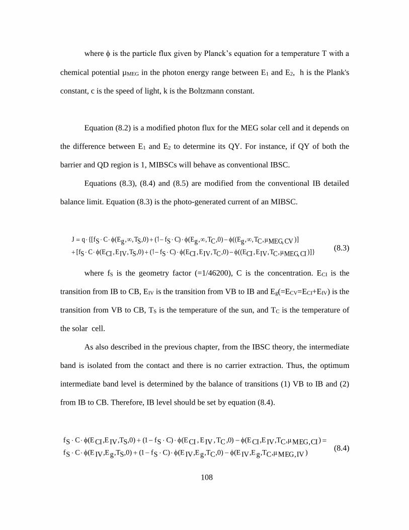
108
where is the particle flux given by Planck’s equation for a temperature T with a
chemical potential µMEG in the photon energy range between E1 and E2, h is the Plank's
constant, c is the speed of light, k is the Boltzmann constant.
Equation (8.2) is a modified photon flux for the MEG solar cell and it depends on
the difference between E1 and E2 to determine its QY. For instance, if QY of both the
barrier and QD region is 1, MIBSCs will behave as conventional IBSC.
Equations (8.3), (8.4) and (8.5) are modified from the conventional IB detailed
balance limit. Equation (8.3) is the photo-generated current of an MIBSC.
)]}CIMEG,μ,CT,IVE,CI((E,0)CT,IVE,CI(EC)Sf(,0)ST,IVE,CI(ECS[f
)]CVMEG,μ,CT,,g((E,0)CT,,g(EC)Sf(,0)ST,,g(ECS{[fqJ
1
1 (8.3)
where fS is the geometry factor (=1/46200), C is the concentration. ECI is the
transition from IB to CB, EIV is the transition from VB to IB and Eg(=ECV=ECI+EIV) is the
transition from VB to CB, TS is the temperature of the sun, and TC is the temperature of
the solar cell.
As also described in the previous chapter, from the IBSC theory, the intermediate
band is isolated from the contact and there is no carrier extraction. Thus, the optimum
intermediate band level is determined by the balance of transitions (1) VB to IB and (2)
from IB to CB. Therefore, IB level should be set by equation (8.4).
)IV,MEG,μC,Tg,EIV(E)0,C,Tg,EIV(E)CSf1()0,S,Tg,EIV(ECSf
)CI,MEG,μC,TIV,ECI(E,0)CT,IVE,CI(EC)Sf1()0,S,TIV,ECI(ECSf
(8.4)

109
And, the chemical potential of MIBSCs is given from equation (8.5) to equation
(8.7).
IV,MEGCI,MEGCV,MEG (8.5)
CICI,MEG V)E(QYq
(8.6)
IVIV,MEG V)E(QYq
(8.7)
8.2.2 Carrier Transitions of MIBSC
IBSCs generate two electrons at the CB based on three transitions. The, IB is
electrically isolated and has no carrier extraction. From reference [113], the conversion
efficiency of the IBSC is similar to triple junction tandem solar cells.
If there is a MEG effect in the IBSC without the restrictions multiple EHPs (QY=2)
and spectral splitting, the generated number of carriers in each transition is 2. For instance,
if the QY is 2, (1) two EHPs are excited from VB to CB, (2) and two from VB to IB and
(3) two EHPs from IB to CB. The total generated EHPs are four at CB due to relations
between QY and spectral splitting. Thus, the procedure of generation of carriers of MIBSC
with QY and spectrum splitting is shown in Fig.8.1. To generate carrier multiplication, the
threshold energy (Eth) for the MEG effect should be two times greater than the bandgap so
that the minimum threshold energy of Eth,CI is 2ECI, Eth,IV is 2EIV and Eth,g = 2Eg where Eth,CI,
Eth,IV and Eth,g are the threshold energies of ECI, EIV and Eg respectively.
The bandgaps should be chosen such that 2ECI < EIV < 2EIV and 2EIV < Eg < 2Eg to
generate two EHPs of each transition, requiring that Eg be greater than two times EIV.
However, Eg is the summation of ECI and EIV which forces Eg to be smaller than 2EIV and
thus the actual QY from VB to IB transitions is 1.

110
ECI 2ECI EIV 2EIV Eg
ECI 2ECI EIV 2EIV
Eg
1
2
1
2
0
0
2Eg
Eph
Eph2Eg
QY
QY
(a)
(b)
Fig.8.1. The QY of three transitions in the MIBSC, (a) Without restrictions for carrier
multiplication, the order of bandgaps is ECI<2ECI < EIV<2EIV <Eg(=ECV) < 2Eg .
(b) The modified carrier generations of MIBSC. ECI<2ECI < EIV<Eg(=ECV) <
2EIV .
Therefore, the conditions for bandgap alignment change to 2ECI<EIV<2EIV and
EIV<Eg<2EIV to avoid spectral overlapping and achieve the maximum QY. The overall
bandgap alignment is shown in equation (8.8) and in Fig.8.1 (b).
IVCVgIVCICI E2)E(EEE2E (8.8)
Under this condition, it is possible to generate more than two EHPS in MIBSC as
is shown in Fig.8.2.

111
ECI EIV Eg
1
2
0Eph
QYIB
VB
CB
IB
VB
CB
ECI EIV Eg
1
2
0Eph
ECI EIV Eg
1
2
0Eph
QYIB
VB
CB
IB
VB
CB
ECI EIV Eg
1
2
0Eph
(a) Number of Electrons = 2
(b) Number of Electrons = 3
(c) Number of Electrons = 3
(d) Number of Electrons = 4
QY
QY
Fig. 8.2. The procedure of generation of carriers in the MIBSC, Eph is the photon energy.
(a) The number of electrons=2. (b) The number of electrons=3 which 2 is from
VB to CB and 1 is IB to CB, (c) The number of electrons=3 which 1 is from VB
to CB and 2 is IB to CB and (d) The number of electrons=4. The 4 EHPs are
generated that 2 is from VB to CB and 2 is from IB to CB.

112
Further, regarding both QY and spectral splitting, the non-overlapping of QY from
the three transitions is also important to optimize the characteristics of MIBSC. For
instance, QY from ECI can be 2 if the spectral splitting region from ECI to EIV is relatively
large.
Thus, Fig. 8.2 provides conditions for MEG such that it generates two EHPs and
increases current. However, if the difference between Eth,CI and EIV is small, the net effect
of increasing current and QY can be negligible. In case of Eg, there can be two EHPs with
no restrictions of spectrum splitting. But, the amount of solar photon energy at high energy
is small so that the increase of light-generated current from Eg to infinity is not large.
Therefore, choosing the proper range of the three bandgaps is important to maximize the
carrier multiplication effect in the MIBSC.
8.2.3 The Possibility of Carrier Multiplication in MIBSC
In Fig.8.2, the author has presented the possible scenarios for the number of carriers
generated in a MIBSC. In this section, the author will discuss which transition is dominant
to generate more than two EHPs. First of all, in a QD region, two EHPs from IB to CB are
shown in Fig. 8.1. Due to the charge neutrality condition, the carrier multiplication
processes in Fig. 8.2 (c) and (d) are impossible without an additional assumption like
another absorption path or doped IB. Even though the spectral splitting makes it possible
to excite carriers from IB to CB to generate two EHPs, the number of EHPs from VB to IB
is 1 which cannot provide another electron to excite from IB to CB by impact ionization.
Here, the author considers Fig 8.2 (a) and (b) in which the generated number of
carriers are two from conventional IBSC theory (see Fig. 8.2 (a)) and three by impact
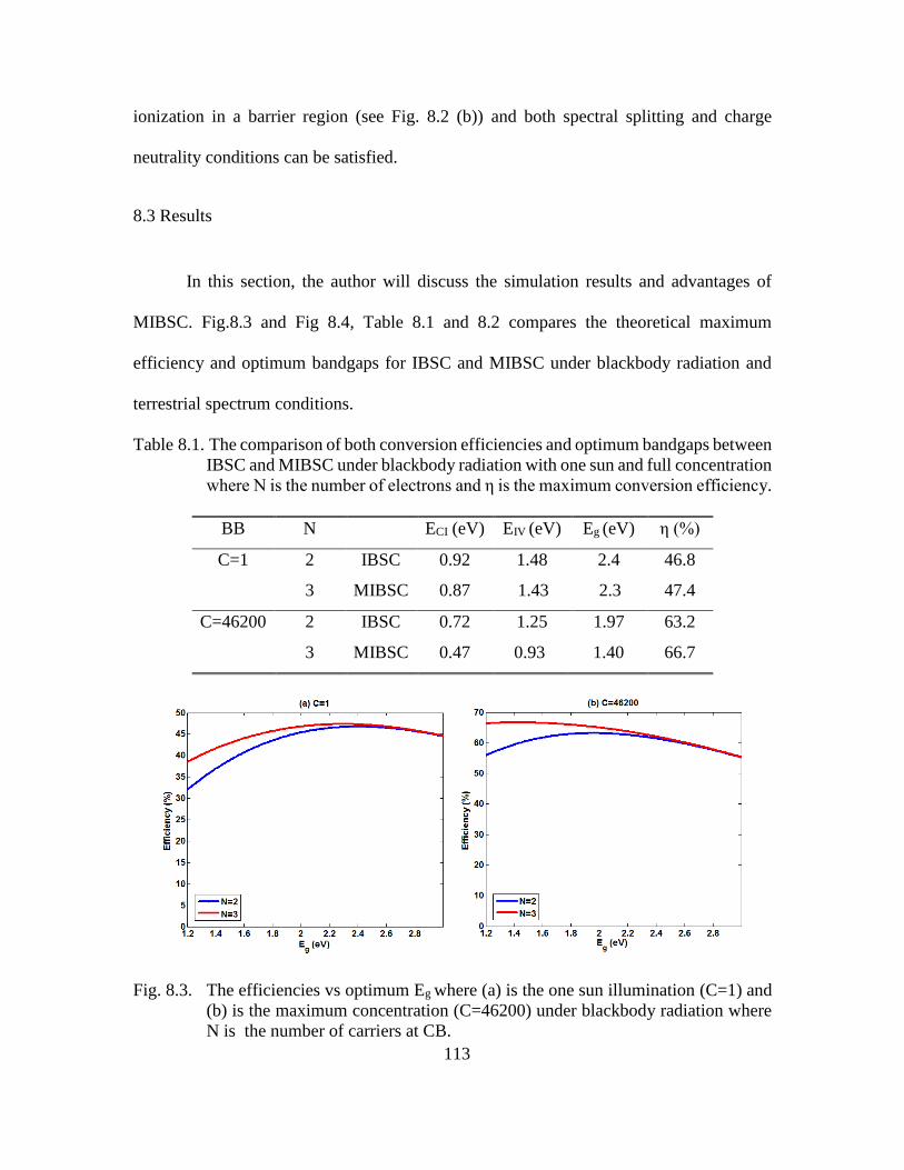
113
ionization in a barrier region (see Fig. 8.2 (b)) and both spectral splitting and charge
neutrality conditions can be satisfied.
8.3 Results
In this section, the author will discuss the simulation results and advantages of
MIBSC. Fig.8.3 and Fig 8.4, Table 8.1 and 8.2 compares the theoretical maximum
efficiency and optimum bandgaps for IBSC and MIBSC under blackbody radiation and
terrestrial spectrum conditions.
Table 8.1. The comparison of both conversion efficiencies and optimum bandgaps between
IBSC and MIBSC under blackbody radiation with one sun and full concentration
where N is the number of electrons and η is the maximum conversion efficiency.
BB N ECI (eV) EIV (eV) Eg (eV) η (%)
C=1 2 IBSC 0.92 1.48 2.4 46.8
3 MIBSC 0.87 1.43 2.3 47.4
C=46200 2 IBSC 0.72 1.25 1.97 63.2
3 MIBSC 0.47 0.93 1.40 66.7
Fig. 8.3. The efficiencies vs optimum Eg where (a) is the one sun illumination (C=1) and
(b) is the maximum concentration (C=46200) under blackbody radiation where
N is the number of carriers at CB.

114
Fig. 8.4. The efficiencies vs optimum Eg where (a) is the one sun illumination (C=1) and
(b) is the maximum concentration (C=46200) under terrestrial spectrum.
Table 8.2. The comparison of both conversion efficiencies and optimum bandgaps between
IBSC and MIBSC under terrestrial spectrum with one sun and full concentration.
AM1.5 N ECI (eV) EIV (eV) Eg (eV) η (%)
C=1
(AM1.5G)
2 IBSC 0.93 1.49 2.42 49.5
3 MIBSC 0.93 1.49 2.42 49.5
C=46200
(AM1.5D)
2 IBSC 0.69 1.22 1.91 67.7
3 MIBSC 0.51 1.00 1.50 67.9
Under blackbody radiation with full concentration shown in Table 8.1 and Fig 8.3,
the theoretical maximum efficiency is increased by 3.2% and the optimum bandgaps are
0.47 eV (=ECI), 0.93 eV (=EIV) and 1.40 eV (=Eg) for which the corresponding QY is 1, 1,
and 2 respectively. Note that the bandgap of the barrier is similar to GaAs (=1.42 eV) and
the QD material can be InAs (=0.36 eV).
Generally, the results clearly indicate that with blackbody radiation and under
concentration conditions, due to carrier multiplications in the three optical transitions, one
can choose low bandgap QD materials and a barrier material with a bandgap up to 2 eV.

115
For Eg above 2 eV the net effect of MEG in MIBSC disappears and the cell becomes
similar to a conventional IBSC.
The bandgap trends for the terrestrial spectrum simulation results for MIBSC in
Table 8.2 and Fig 8.4are similar to those found for blackbody radiation. However, a
difference of only 0.2 % in the maximum conversion efficiency is found between MIBSC
and IBSC under full concentration conditions because of fluctuations of the terrestrial
spectrum. The general trends for the optimum three bandgaps are similar and the three
optimum bandgaps are 0.51 eV(=ECI), 1.00 eV(=EIV) and 1.51 eV(=Eg) with corresponding
QYs of 1, 1, and 2. The overall number of generated carriers is 3 at the maximum
conversion efficiency point.
The optimum bandgaps under one sun with blackbody radiation or the terrestrial
spectrum is slightly lowered compared to conventional IBSC due to the two carrier
generations from Eg. The optimum bandgaps under the one sun terrestrial spectrum is the
same as for a conventional IBSC due to the limited spectrum range. Thus, it is absolutely
necessary to use the light concentrator to get the benefits.
From all above results, the author considers the possible material candidates of
MIBSC where there are similar optimum bandgaps from both blackbody radiation and the
terrestrial spectrum under concentration. Currently, there are reports of MEG or carrier
multiplication phenomena in III-V materials such as InAs [43], InP [84], InN [85], InSb
[148], and GaAs [149],[150]measured by terahertz pump-probe measurements. Among
these materials, promising combinations such as InAs/InP, InAs/GaAs, InN/InGaN and
InSb/AlInSb are potential candidates for MIBSC.
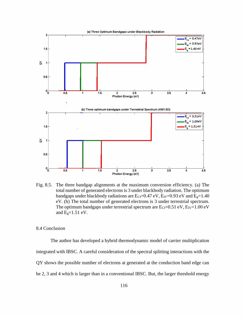
116
Fig. 8.5. The three bandgap alignments at the maximum conversion efficiency. (a) The
total number of generated electrons is 3 under blackbody radiation. The optimum
bandgaps under blackbody radiations are ECI=0.47 eV, EIV=0.93 eV and Eg=1.40
eV. (b) The total number of generated electrons is 3 under terrestrial spectrum.
The optimum bandgaps under terrestrial spectrum are ECI=0.51 eV, EIV=1.00 eV
and Eg=1.51 eV.
8.4 Conclusion
The author has developed a hybrid thermodynamic model of carrier multiplication
integrated with IBSC. A careful consideration of the spectral splitting interactions with the
QY shows the possible number of electrons at generated at the conduction band edge can
be 2, 3 and 4 which is larger than in a conventional IBSC. But, the larger threshold energy

117
from the valence band to intermediate band does not contribute to MEG (the effective QY
of EIV is 1) due to the overlap of QY between ECI and EIV. Other transitions such ECI and
Eg can make two EHPs. So, the overall efficiencies with and without concentration are only
slightly enhanced. After accounting for solar spectral splitting and QY, the possible
additional number of carriers generated is 3 due to transition from VB to CB because of
charge neutrality condition and metallic properties of IB. Increasing the concentration of
light is the only way to boost the MEG effect in the IBSC. Under these conditions, more
incident photon energy into MIBSC has the possibility of increasing the number of carriers.

118
CHAPTER 9
CONCLUSION
The author has proposed several types of hybrid solar cell models by
thermodynamics to overcome existing theoretical limit of PV cells and suggest suitable
materials with nanostructures. The potential benefits of novel concept solar cells can have
multi-physics effects in one solar cell due to integrating two concepts such as (1) multiple
exciton generation (MEG) and tandem, (2) intermediate band (IB) and tandem and (3)
MEG and IB while maintaining the properties of conventional solar cells. The development
of hybrid concepts uniquely the realization of ultra-high solar cell efficiencies, as even
including a single advanced concept approach, efficiencies substantially over 50% at
realistic concentration ratios and with non-ideal assumption do not exist.
First, the author investigated the limiting efficiency of multiple exciton generation
solar cell with non-ideal effect such as delayed threshold energy under concentration. The
ideal quantum yield offers a large improvement of theoretical conversion efficiency to
surpass the Shockley and Queisser limit. But, when examining non-ideal quantum yield
and its threshold energy above the ideal values, the effect of carrier multiplications of single
junction solar cell was reduced. In particular, the benefit disappears for one-sun conditions,
so using concentrators is necessary to provide advantages in the theoretical conversion
efficiency. Furthermore, the threshold energy should be located at between two and three
times of bandgap materials to maximize the generating multiple electron and hole pairs.
Second, the thermodynamic limit of MEG with multijunction (MJMEG) has been
proposed and calculated to upgrade the model of current tandem solar cells. General
multjunction solar cells are presently leading the efficiency of PV cells. However,

119
disadvantages like defects of interfacial layer cause the limit to monolithic growth and
number of junctions. Thus, utilizing MEG with multijunction in nanostructures can
contribute to enhance the characteristics of theoretical efficiency and use low bandgap
materials. Its calculated efficiency is improved at the low number of junctions to maximize
the carrier multilplication. However, the increased number of junction in this hybrid solar
cell does not provide such large benefits due to decreasing the possible maximum quantum
yield of each junction.
Third, after studying this MJMEG solar cell, the author focused on silicon
nanostructure solar cells for MEG and MJMEG applications. Silicon has substantial
possibility to use the nano-materials because even if silicon is an indirect bangap material,
it can be direct bandgap materials in nanostructures due to excellent quantum confinement.
The author has investigated the limiting efficiency of silicon MEG with concentration
under terrestrial spectrum. Then, limiting efficiencies of Si MJMEG has also calculated.
Silicon cover visible range of photon energy so that silicon nanostructures can use for the
upper junction of MJMEG. Based on this, the author has investigated the appropriate
materials for bottom junction such as InAs or InN. Furthermore, the compatibility of these
material combinations also investigated to improve the quantum confinements.
Forth, the author presented the experiment results of a silicon nanostructured solar
cell. The periodic silicon nanowire defined by electron beam lithography shows the
improved short-circuit current. But, due to low open-circuit voltages and fill factors, related
to the large rear junction area, the overall efficiency was low. Further, the optical resonance
at the bandgap of amorphous silicon offer to beneficial effect of low reflectance. However,
the number of nanostructures is also important to regard to reduce the reflectance the entire

120
range of wavelength to increase the short-circuit current. With improvements in the rear
surface structure, the proposed device offers an approach to realization of a silicon
nanostructured solar cell.
Fifth, an alternative to overcoming tandem solar cells’ limit is using an intermediate
band solar cell. The most important assumption of intermediate band solar cell is three
strong light-absorptions in one junction with intermediateband. Thus, it has three carrier
transitions and its theoretical efficiency under full concentration is similar to triple junction
tandem solar cells. The tandem configuration of double stacked intermediate band solar
cells shows the similar theoretical efficiency of five or six junction tandem solar cells. Thus,
this configuration reduces the number of junctions compared to tandem solar cells,
enabling the efficiency of 5 or 6 junction device with only 4 materials. In material
investigations, Si/Ge or III-V for the bottom junction with III-V nitride for the upper
junction shows appropriate combinations for in an independent connection. For series-
connection, near 0.9 eV material for the bottom junction and a high bandgap of 3eV
materials (III-V or II-VI) for the top junction can be used. The materials for quantum dot
are still require further materials to searches to optimize the properties and quantum
confinement for efficient managing of photons.
The final discussion for novel concept of PV model is carrier multiplication at the
intermediate band solar cells. The both concepts of solar cells can use the low bandgap
materials to control the incoming photon efficiently. To investigate the possible regions of
carrier multiplications, it is necessary to investigate the spectral splitting. The transition
between (1) the intermediate band to conduction band and (2) the valence band to
conduction band have the largest possibility of realizing carrier multiplication. However,

121
the charge neutrality at the intermediate band must satisfy with valence the number of
electron and hole pairs. A doped intermediate band can be considered to replace metallic
properties of intermediate band.
Overall, the hybrid concepts of limiting efficiency model provide substantial
potential to improve the efficiency of solar cells through developing multi-physical effects
in one solar cell. Even if the proposed of third generation PV cells have large benefits to
surpass the single junction limit, the suggested detailed balance limit of hybrid solar cells
in this dissertation offer multiple advantages to overcoming the existing limits. Moreover,
these hybrid model can be achieved by the existing solar cell materials such as silicon by
using nanostructures such as quantum dots.
The detailed balance limit or thermodynamic limit can describe only the ideal PV
model that it is not considered the real physical parameters of solar cells. Thus, it is also
necessary to exploit the realistic hybrid solar cells model including multi-physics
parameters and find ways to fabricate with appropriate material and structures.

122
REFERENCES
[1] “International Energy Outlook 2013,” US Energy Information Administration,
Department of Energy, published July 2013.
[2] “Annual Energy Review 2010 with projections to 2040,” US Energy Information
Administration, Department of Energy, published April 2013.
[3] “Renewable energy technologies: cost analysis series,” vol.1, no. 4/5, International
Renewable Energy Agency published in 2012.
[4] M. A. Green, “Third generation photovoltaics: Ultra-high conversion efficiency at
low cost,” Progress in Photovoltaics: Research and Applications, vol. 9, no. 2, pp.
123-135, 2001.
[5] “Best Research Cell Efficiency,” National Renewable Energy Laboratory,
published 2013, (http://www.nrel.gov/ncpv/images/efficiency_chart.jpg)
[6] M. A. Green, K. Emery, Y. Hishikawa, W. Warta, and E. D. Dunlop, “Solar cell
efficiency tables (version 42),” Progress in Photovoltaics: Research and
Applications, vol. 21, no. 5, pp. 827-837, 2013.
[7] PVCDROM, “http://pveducation.org/pvcdrom”
[8] J. Zhao, A. Wang, and M. A. Green, “24·5% Efficiency silicon PERT cells on MCZ
substrates and 24·7% efficiency PERL cells on FZ substrates,” Progress in
Photovoltaics: Research and Applications, vol. 7, no. 6, pp. 471-474, 1999.
[9] B. M. Kayes, N. Hui, R. Twist, S. G. Spruytte, F. Reinhardt, I. C. Kizilyalli, and G.
S. Higashi, "27.6% Conversion efficiency, a new record for single-junction solar
cells under 1 sun illumination." In Proc. Of 37th IEEE Phovovoltaic Special
Conference, pp. 000004-000008., Seattle, WA, 2011.
[10] http://panasonic.co.jp/corp/news/official.data/data.dir/2014/04/en140410-
4/en140410-4.html
[11] S.P. Philipps, E. Essig, S. Heckelmann, R. Kellenbenz, V. Klinger, M. Niemeyer,
D. Lackner, F. Dimroth, “Overview about Technology Perspectives for High
Efficiency Solar Cells for Space and Terrestrial Applications,” Presented in 28th
European Photovoltaic Solar Energy Conference and Exhibition 2013
Paris,France,
http://www.ise.fraunhofer.de/de/veroeffentlichungen/konferenzbeitraege/konferen
zbeitraege-2013/28th-eupvsec/bett.pdf

123
[12] W. Shockley and H.J. Queisser. “Detailed balance limit of efficiency of p‐n
junction solar cells”, Journal of Applied Physics, vol. 32, no.3, pp. 510-519, 1961.
[13] S. Kolodinski, J. H. Werner, T. Wittchen, and H. J. Queisser, “Quantum efficiencies
exceeding unity due to impact ionization in silicon solar cells,” Applied Physics
Letters, vol. 63, no. 17, pp. 2405-2407, 1993.
[14] J. H. Werner, S. Kolodinski, and H. J. Queisser, “Novel optimization principles and
efficiency limits for semiconductor solar cells,” Physical Review Letters, vol. 72,
no. 24, pp. 3851-3854, 1994.
[15] A. Luque, and A. Martí, “Increasing the efficiency of ideal solar cells by photon
induced transitions at intermediate levels,” Physical Review Letters, vol. 78, no. 26,
pp. 5014-5017, 1997.
[16] S. A. Blokhin, A. V. Sakharov, A. M. Nadtochy, A. S. Pauysov, M. V. Maximov,
N. N. Ledentsov, A. R. Kovsh, S. S. Mikhrin, V. M. Lantratov, S. A. Mintairov, N.
A. Kaluzhniy, and M. Z. Shvarts, “AlGaAs/GaAs photovoltaic cells with an array
of InGaAs QDs,” Semiconductors, vol. 43, no. 4, pp. 514-518, 2009.
[17] P. Atkins, “The Laws of Thermodynamics: A very short introduction,” Oxford
University Press, April, 2010
[18] A. De Vos, “Endoreversible Thermodynamics of Solar Energy Conversion”,
Oxford University Press, 1992.
[19] M. C. Beard, and R. J. Ellingson, “Multiple exciton generation in semiconductor
nanocrystals: Toward efficient solar energy conversion,” Laser & Photonics
Reviews, vol. 2, no. 5, pp. 377-399, 2008.
[20] S. P. Bremner, M. Y. Levy, and C. B. Honsberg, “Analysis of tandem solar cell
efficiencies under AM1.5G spectrum using a rapid flux calculation method,”
Progress in Photovoltaics: Research and Applications, vol. 16, no. 3, pp. 225-233,
2008.
[21] A. D. Vos, “Detailed balance limit of the efficiency of tandem solar cells,” Journal
of Physics D: Applied Physics, vol. 13, no. 5, pp. 839-846, 1980.
[22] M. Wiemer, V. Sabnis, and H. Yuen, “43.5% efficient lattice matched solar cells,”
In Proc. Of SPIE High and low concentrator systems for electric applications VI,
San Diego, CA, pp. 810804-810804, 2011.
[23] “World Record Solar Cell with 44.7% Efficiency,” press released September, 2013
http://www.ise.fraunhofer.de/en/press-and-media/press-
releases/presseinformationen-2013/world-record-solar-cell-with-44.7-efficiency.

124
[24] J. Lee and and C. B. Honsberg, "Impact of threshold energy of multiple exciton
generation solar cells." in Proc. 39th IEEE Photovoltaic Spec. Conf., Tampa, FL,
2013, pp. 1050-1053.
[25] R. Brendel, J. H. Werner, and H. J. Queisser, “Thermodynamic efficiency limits for
semiconductor solar cells with carrier multiplication,” Solar Energy Materials and
Solar Cells, vol. 41–42, no. 0, pp. 419-425, 1996.
[26] A. De Vos, and B. Desoete, “On the ideal performance of solar cells with larger-
than-unity quantum efficiency,” Solar Energy Materials and Solar Cells, vol. 51,
no. 3–4, pp. 413-424, 1998.
[27] J. H. Werner, R. Brendel, and H. J. Queisser, “Radiative efficiency limit of
terrestrial solar cells with internal carrier multiplication,” Applied Physics Letters,
vol. 67, no. 7, pp. 1028-1030, 1995.
[28] J.H. Werner, R. Brendel, H.J. Queisser, “New upper efficiency limits for
semiconductor solar cells,” in: Proceedings of the IEEE 1st World Conference on
Photovoltaic Energy Conversion, Waikoloa, HI, USA, 1994, pp. 1742–1745.
[29] R. J. Ellingson, M. C. Beard, J. C. Johnson, P. Yu, O. I. Micic, A. J. Nozik, A.
Shabaev, and A. L. Efros, “Highly efficient multiple exciton generation in colloidal
PbSe and PbS Quantum Dots,” Nano Letters, vol. 5, no. 5, pp. 865-871, 2005.
[30] A. Luque, and A. Martí, “A metallic intermediate band high efficiency solar cell,”
Progress in Photovoltaics: Research and Applications, vol. 9, no. 2, pp. 73-86, 2001.
[31] M. A. Green, “Third generation photovoltaics: solar cells for 2020 and beyond,”
Physica E: Low-dimensional Systems and Nanostructures, vol. 14, no. 1–2, pp. 65-
70, 2002.
[32] A. J. Nozik, “Quantum dot solar cells,” Physica E: Low-dimensional Systems and
Nanostructures, vol. 14, no. 1–2, pp. 115-120, 2002.
[33] J. A. Burton, “Electron emission from avalanche breakdown in silicon,” Physical
Review, vol. 108, no. 5, pp. 1342-1343, 1957.
[34] V. S. Vavilov, “On photo-ionization by fast electrons in germanium and silicon,”
Journal of Physics and Chemistry of Solids, vol. 8, no. 0, pp. 223-226, 1959.
[35] O. Christensen, “Quantum efficiency of the internal photoelectric effect in silicon
and germanium,” Journal of Applied Physics, vol. 47, no. 2, pp. 689-695, 1976.
125
[36] F. Capasso, P. M. Petroff, W. B. Bonner, and S. Sumski, “Investigation of
microplasmas in InP avalanche photodiodes,” Electron Device Letters, IEEE, vol.
1, no. 3, pp. 27-29, 1980.
[37] M. C. Beard, A. G. Midgett, M. C. Hanna, J. M. Luther, B. K. Hughes, and A. J.
Nozik, “Comparing multiple exciton generation in quantum dots to impact
ionization in bulk semiconductors: Implications for enhancement of solar energy
conversion,” Nano Letters, vol. 10, no. 8, pp. 3019-3027, 2010.
[38] R. D. Schaller, M. Sykora, J. M. Pietryga, and V. I. Klimov, “Seven Excitons at a
Cost of One: Redefining the limits for conversion efficiency of photons into charge
carriers,” Nano Letters, vol. 6, no. 3, pp. 424-429, 2006.
[39] S. J. Kim, W. J. Kim, Y. Sahoo, A. N. Cartwright, and P. N. Prasad, “Multiple
exciton generation and electrical extraction from a PbSe quantum dot
photoconductor,” Applied Physics Letters, vol. 92, no. 3, pp. 031107 – 031107-3,
2008.
[40] G. Nair, and M. G. Bawendi, “Carrier multiplication yields of CdSe and CdTe
nanocrystals by transient photoluminescence spectroscopy,” Physical Review B,
vol. 76, no. 8, pp. 081304-1 081304-4, 2007.
[41] R. D. Schaller, M. A. Petruska, and V. I. Klimov, “Effect of electronic structure on
carrier multiplication efficiency: Comparative study of PbSe and CdSe
nanocrystals,” Applied Physics Letters, vol. 87, no. 25, pp. 253102-1-253102-3,
2005.
[42] J. J. H. Pijpers, E. Hendry, M. T. W. Milder, R. Fanciulli, J. Savolainen, J. L. Herek,
D. Vanmaekelbergh, S. Ruhman, D. Mocatta, D. Oron, A. Aharoni, U. Banin, and
M. Bonn, “Carrier multiplication and its reduction by photodoping in colloidal InAs
quantum dots,” The Journal of Physical Chemistry C, vol. 111, no. 11, pp. 4146-
4152, 2007.
[43] R. D. Schaller, J. M. Pietryga, and V. I. Klimov, “Carrier multiplication in InAs
nanocrystal quantum dots with an onset defined by the energy conservation limit,”
Nano Letters, vol. 7, no. 11, pp. 3469-3476, 2007.
[44] M. C. Beard, K. P. Knutsen, P. Yu, J. M. Luther, Q. Song, W. K. Metzger, R. J.
Ellingson, and A. J. Nozik, “Multiple exciton generation in colloidal silicon
nanocrystals,” Nano Letters, vol. 7, no. 8, pp. 2506-2512, 2007.
[45] J. A. McGuire, J. Joo, J. M. Pietryga, R. D. Schaller, and V. I. Klimov, “New
aspects of carrier multiplication in semiconductor nanocrystals,” Accounts of
Chemical Research, vol. 41, no. 12, pp. 1810-1819, 2008.
126
[46] M. T. Trinh, A. J. Houtepen, J. M. Schins, T. Hanrath, J. Piris, W. Knulst, A. P. L.
M. Goossens, and L. D. A. Siebbeles, “In spite of recent doubts carrier
multiplication does occur in PbSe nanocrystals,” Nano Letters, vol. 8, no. 6, pp.
1713-1718, 2008.
[47] M. C. Beard, A. G. Midgett, M. Law, O. E. Semonin, R. J. Ellingson, and A. J.
Nozik, “Variations in the quantum efficiency of multiple exciton generation for a
series of chemically treated PbSe nanocrystal Films,” Nano Letters, vol. 9, no. 2,
pp. 836-845, 2009.
[48] J. J. H. Pijpers, R. Ulbricht, K. J. Tielrooij, A. Osherov, Y. Golan, C. Delerue, G.
Allan, and M. Bonn, “Assessment of carrier-multiplication efficiency in bulk PbSe
and PbS,” Nature Physics, vol. 5, no. 11, pp. 811-814, 2009.
[49] P. Tyagi, and P. Kambhampati, “False multiple exciton recombination and multiple
exciton generation signals in semiconductor quantum dots arise from surface
charge trapping,” The Journal of Chemical Physics, vol. 134, no. 9, pp. 094706-1-
094706-10, 2011.
[50] A. G. Midgett, H. W. Hillhouse, B. K. Hughes, A. J. Nozik, and M. C. Beard,
“Flowing versus Static conditions for measuring multiple exciton generation in
PbSe quantum dots,” The Journal of Physical Chemistry C, vol. 114, no. 41, pp.
17486-17500, 2010.
[51] M. T. Trinh, L. Polak, J. M. Schins, A. J. Houtepen, R. Vaxenburg, G. I. Maikov,
G. Grinbom, A. G. Midgett, J. M. Luther, M. C. Beard, A. J. Nozik, M. Bonn, E.
Lifshitz, and L. D. A. Siebbeles, “Anomalous independence of multiple exciton
generation on different group IV−VI quantum dot architectures,” Nano Letters, vol.
11, no. 4, pp. 1623-1629, 2011.
[52] O. E. Semonin, J. M. Luther, S. Choi, H.-Y. Chen, J. Gao, A. J. Nozik, and M. C.
Beard, “Peak external photocurrent quantum efficiency exceeding 100% via MEG
in a quantum dot solar cell,” Science, vol. 334, no. 6062, pp. 1530-1533, 2011.
[53] P. D. Cunningham, J. E. Boercker, E. E. Foos, M. P. Lumb, A. R. Smith, J. G.
Tischler, and J. S. Melinger, “Enhanced multiple exciton generation in quasi-one-
dimensional semiconductors,” Nano Letters, vol. 11, no. 8, pp. 3476-3481, 2011.
[54] M. C. Hanna, and A. J. Nozik, “Solar conversion efficiency of photovoltaic and
photoelectrolysis cells with carrier multiplication absorbers,” Journal of Applied
Physics, vol. 100, no. 7, pp. 074510-1-074510-8, 2006.
[55] Y. Takeda, and T. Motohiro, “Requisites to realize high conversion efficiency of
solar cells utilizing carrier multiplication,” Solar Energy Materials and Solar Cells,
vol. 94, no. 8, pp. 1399-1405, 2010.

127
[56] M. C. Hanna, M. C. Beard, and A. J. Nozik, “Effect of solar concentration on the
thermodynamic power conversion efficiency of quantum-dot solar cells exhibiting
multiple exciton generation,” The Journal of Physical Chemistry Letters, vol. 3, no.
19, pp. 2857-2862, 2012.
[57] American Society for Testing and Materials- "Standard tables for reference solar
spectral irradiances: Direct normal and hemispherical on 37° Tilted Surface,"
[58] A. De Vos, “Detailed balance limit of the efficiency of tandem solar cells”, Journal
of Physics. D: Applied Physics, vol. 13, pp. 839-846, 1980.
[59] M. S. Leite, R. L. Woo, J. N. Munday, W. D. Hong, S. Mesropian, D. C. Law, and
H. A. Atwater, “Towards an optimized all lattice-matched
InAlAs/InGaAsP/InGaAs multijunction solar cell with efficiency > 50%,” Applied
Physics Letters, vol. 102, no. 3, pp. 033901-5-1-033901-5, 2013.
[60] J. Lee and C. B. Honsberg, “Limiting efficiencies over 50% using multijunction
solar cells with multiple exciton generation”, in Proc. 38th IEEE Photovoltaic Spec.
Conf., Austin, TX, 2012, pp 62-67.
[61] J. Lee, and C. B. Honsberg, “Limiting Efficiencies of Multijunction Solar Cells
With Multiple Exciton Generation,” Photovoltaics, IEEE Journal of, vol. 4, no. 3,
pp. 874-880, 2014.
[62] E. D. Jackson, “Areas for improvement of the semiconductor solar energy
converter”, Trans. Conf. on Use of Solar Energy, Tucson, AZ, Oct.31-Nov.1, 1955,
pp 122-126.
[63] R. L. Moon, L. W. James, H. A. VanderPlas, T. O. Yep, G. A. Antypas, and Y.
Chai, “ Multigap solar cell requirements and the performance of AlGaAs and Si
cells in concentrated sunlight”, in Proc. 13th IEEE Photovoltaic Spec. Conf., 1978,
pp 859-867.
[64] D. Friedman, S. Kurtz, K. Bertness, A. Kibbler, C.Kramer, J. Olson, D. King, B.
Hansen, and J. Snyder, “GaInP/GaAs monolithic tandem concentrator cells”, in.
Proc. 24th IEEE Photovoltaic Spec. Conf. Waikoloa, HI, 1994, pp. 1829–1832.
[65] S. R. Kurtz, D. Myers, and J. M. Olson, “Projected performance of three- and four-
junction devices using GaAs and GaInP”, in. Proc. 26th IEEE Photovoltaic Spec.
Conf., Anaheim, CA, 1997, pp. 875-878.
[66] R. R. King, D. C. Law, K. M. Edmondson, C. M. Fetzer, G. S. Kinsey, H. Yoon, R.
A. Sherif, and N. H. Karam, “40% efficient metamorphihc GaInP/GaInAs/Ge
multijunction solar cells”, Applied Physics Letters, vol. 90, no. 18, pp. 183516-1-
183516-3, 2007.
128
[67] R. R. King, R. A. Sherif, D. C. Law, J. T. Yen, M. Haddad, C. M. Fetzer,K. M.
Edmondson, G. S. Kinsey, H. Yoon, M. Joshi, S. Mesropian, H. L. Cotal, D. D.
Krut, J. H. Ermer, and N. H. Karam, “New horizons in III-V multijunction
terrestrial concentrator cell research”, in Proc. the 21st Eur. Photovoltaic Solar
Energy Conf., Dresden, Germany, pp. 124-128.
[68] R. R. King, D. C. Law, C. M. Fetzer, R. A. Sherif, K. M. Edmondson, S. Kurtz, G.
S. Kinsey, H. L. Cotal, D. D. Krut, J. H. Ermer, and N. H. Karam, "Pathways to 40%
efficient concentrator photovoltaics”, in Proc. 20th Eur. Photovoltaic Solar Energy
Conf., Barcelona, Spain, 2005, pp. 118-123.
[69] J. F. Geisz, S. R. Kurtz, M. W. Wanlass, J. S. Ward, A. Duda, D. J. Friedman, J. M.
Olson, W. E. McMahon, T. Moriarty, and J. Kiehl, “High-efficiency
GaInP/GaAs/InGaAs triple-junction solar cells grown inverted with a metamorphic
bottom junction”, Applied Physics Letters., vol. 91.no. 2, pp. 023502-1-023502-1,
2007.
[70] J.F. Geisz, D. J. Friedman, J.S. Ward, A. Duda, W. J. Olavarroa, T. E. Moriatry,
J.T. Kiehl, M.J. Romero, A.G. Norman and K. M. Jones, “40.8% efficient inverted
triple-junction solar cell with two independently metamorphic junctions”, Applied
Physics Letters, vol. 93., pp. 123505-1- 123505-3, 2008.
[71] R. R. King, A. Boca, W. Hong, X.-Q. Liu, D. Bhusari, D. Larrabee, K. M.
Edmondson, D. C. Law, C. M. Fetzer, S. Mesropian, and N. H. Karam, “Band-gap-
engineered architectures for high-efficiency multijunction concentrator solar cells”,
in Proc. 24th Eur. Photovoltaic Solar Energy Conf., 2009, pp. 55-61.
[72] S. Wojtczuk, P. Chiu, X. Zhang, D. Derkacs, C. Harris, D. Pulver, and M. Timmons,
“InGaP/GaAs/InGaAs concentrators using Bi-facial epigrowth”, in Proc. 35th
IEEE Photovoltaic Spec. Conf., Honolulu, HI, 2010, pp. 1259-1264.
[73] M. Yamaguchi, "III-V compound multi-junction solar cells: Present and future",
Solar Energy Materials and Solar Cells., vol. 75, no. 1–2,pp. 261-269, 2003
[74] M. Courel, J. C. Rimada, and L. Hernández, “GaAs/GaInNAs quantum well and
superlattice solar cell”, Applied Physics Letters., vol. 100, no. 7, pp. 073508-1-
073508-4, 2012.
[75] A. Martí, and G. L. Araújo, “Limiting efficiencies for photovoltaic energy
conversion in multigap systems,” Solar Energy Materials and Solar Cells, vol. 43,
no. 2, pp. 203-222, 1996.

129
[76] A. S. Brown, and M. A. Green, “Detailed balance limit for the series constrained
two terminal tandem solar cell,” Physica E: Low-dimensional Systems and
Nanostructures, vol. 14, no. 1–2, pp. 96-100, 2002
[77] H. Cotal, C. Fetzer, J. Boisvert, G. Kinsey, R. King, P. Hebert, H. Yoon, and N.
Karam, “III-V multijunction solar cells for concentrating photovoltaics,” Energy &
Environmental Science, vol. 2, no. 2, pp. 174-192, 2009.
[78] B. Beaumont, P. Garabedian, G. Nataf, J. C. Guillaume, P. Gilbart, and C. Verie,
"Mechanically stacked two-tandem concentrator solar cell concept.", in Proc. 21st
IEEE Photovoltaic Spec. Conf., 1990, pp. 47-52.
[79] P. T. Landsberg and V. Badescu, “Solar cell thermodynamics including multiple
impact ionization and concentration of radiation”, Journal of Physics D.: Applied
Physics., vol. 35, pp. 1236-1240, 2002.
[80] P. Würfel, “Solar energy conversion with hot electrons from impact ionisation,”
Solar Energy Materials and Solar Cells, vol. 46, no. 1, pp. 43-52, 1997.
[81] R. D. Schaller, and V. I. Klimov, “High efficiency carrier multiplication in PbSe
nanocrystals: Implications for Solar Energy Conversion,” Physical Review Letters,
vol. 92, no. 18, pp. 186601-1-186601-4, 2004.
[82] A.J. Nozik, “Multiiple exciton generation in semiconductor quantum dots”,
Chemical Physics Letters, vol. 457, pp. 3-11, 2008.
[83] S. K. Stubbs, S. J. O. Hardman, D. M. Graham, B. F. Spencer, W. R. Flavell, P.
Glarvey, O. Masala, N. L. Pickett, and D. J. Binks, “Efficient carrier multiplication
in InP nanoparticles,” Physical Review B, vol. 81, no. 8, pp. 081303-1-081303-4,
2010.
[84] S. A. Jensen, J. Versluis, E. Canovas, J. J. H. Pijpers, I. R. Sellers, and M. Bonn,
“Carrier multiplication in bulk indium nitride,” Applied Physics Letters, vol. 101,
no. 22, pp. 222113-1-222113-4, 2012.
[85] F. Dimroth, “High-efficiency solar cells from III-V compound semiconductors,”
physica status solidi (c), vol. 3, no. 3, pp. 373-379, 2006.
[86] J. Lee, S. M. Goodnick, and C. B. Honsberg, "Limiting efficiency of silicon based
nanostructure solar cells for multiple exciton generation." In Proc. Of 39th IEEE
Phovovoltaic Special Conference, pp. 1046-1049, Tampa, MI, 2013.
[87] C. Delerue, G. Allan, and M. Lannoo, “Theoretical aspects of the luminescence of
porous silicon,” Physical Review B, vol. 48, no. 15, pp. 11024-11036, 1993.

130
[88] W. A. Su, and W. Z. Shen, “A statistical exploration of multiple exciton generation
in silicon quantum dots and optoelectronic application,” Applied Physics Letters,
vol. 100, no. 7, pp. 071111-1-071111-5, 2012.
[89] C. Meier, A. Gondorf, S. Lüttjohann, A. Lorke, and H. Wiggers, “Silicon
nanoparticles: Absorption, emission, and the nature of the electronic bandgap,”
Journal of Applied Physics, vol. 101, no. 10, pp. 103112-1-103112-7, 2007.
[90] S. Baskoutas, and A. F. Terzis, “Size-dependent band gap of colloidal quantum
dots,” Journal of Applied Physics, vol. 99, no. 1, pp. 013708-1-013708-4, 2006.
[91] D. Timmerman, J. ValentaJ, K. Dohnalova, W.D.A.M. de Boer, and T.
Gregorkiewicz, “Step-like enhancement of luminescence quantum yield of silicon
nanocrystals,” Nature Nanotechnology, vol. 6, no. 11, pp. 710-713, 2011.
[92] W. Wei, X.-Y. Bao, C. Soci, Y. Ding, Z.-L. Wang, and D. Wang, “Direct
Heteroepitaxy of Vertical InAs Nanowires on Si Substrates for Broad Band
Photovoltaics and Photodetection,” Nano Letters, vol. 9, no. 8, pp. 2926-2934, 2009.
[93] K. Tomioka, J. Motohisa, S. Hara, and T. Fukui, “Control of InAs Nanowire
Growth Directions on Si,” Nano Letters, vol. 8, no. 10, pp. 3475-3480, 2008.
[94] B. Ehrler, K. P. Musselman, M. L. Bohm, R. H. Friend, and N. C. Greenham,
“Hybrid pentacene/a-silicon solar cells utilizing multiple carrier generation via
singlet exciton fission,” Applied Physics Letters, vol. 101, no. 15, pp. 153507-1-
153507-3, 2012.
[95] H. Shujuan, and C. Gavin, “Sputter-grown Si quantum dot nanostructures for
tandem solar cells,” Journal of Physics D: Applied Physics, vol. 46, no. 2, pp.
024003-1-024003-8, 2013.
[96] M. A. Green, “Recent developments in photovoltaics,” Solar Energy, vol. 76, no.
1–3, pp. 3-8, 2004.
[97] E. Garnett, and P. Yang, “Light trapping in silicon nanowire solar cells,” Nano
Letters, vol. 10, no. 3, pp. 1082-1087, 2010.
[98] E. A. Alsema, “Energy pay-back time and CO2 emissions of PV systems,” Progress
in Photovoltaics: Research and Applications, vol. 8, no. 1, pp. 17-25, 2000.
[99] B. Dale B, H. G. Rudenberg “High efficiency silicon solar cells,” In: Proceedings
of the 14th Annual Power Sources Conference. Proceedings of the 14th Annual
Power Sources Conference. U.S. Army Signal Research and Development Lab;
1960. p. 22.

131
[100] M. Taguchi, A. Yano, S. Tohoda, K. Matsuyama, and Y. Nakamura, paper,
presented at the Thirty-ninth IEEE Photovoltaic Specialists Conference, 2013
[101] S. Y. Herasimenka, W. J. Dauksher, and S. G. Bowden, “>750 mV open circuit
voltage measured on 50 μm thick silicon heterojunction solar cell,” Applied Physics
Letters, vol. 103, no. 5, pp. 053511-1-053511-4, 2013.
[102] C. Green, “Silicon Nanowires for Optical Light Trapping in Solar Cells” , on 2013
Research Accomplishments, National Nanotechnology Intrastructure Network
Research Experience for Undergraduates Program, pp. 178-179, 2013
“http://nnin.org/sites/default/files/2013_reu_ra/2013nninRA_1Book_0.pdf”
[103] G. Conibeer, M. Green, R. Corkish, Y. Cho, E.-C. Cho, C.-W. Jiang, T.
Fangsuwannarak, E. Pink, Y. Huang, T. Puzzer, T. Trupke, B. Richards, A. Shalav,
and K.-l. Lin, “Silicon nanostructures for third generation photovoltaic solar cells,”
Thin Solid Films, vol. 511–512, no. 0, pp. 654-662, 2006.
[104] S. Mokkapati, and K. R. Catchpole, “Nanophotonic light trapping in solar cells,”
Journal of Applied Physics, vol. 112, no. 10, pp. 101101-1- 101101-19, 2012.
[105] F. Priolo, T. Gregorkiewicz, M. Galli, and T. F. Krauss, “Silicon nanostructures for
photonics and photovoltaics,” Nature Nanotechnology, vol. 9, no. 1, pp. 19-32,
2014.
[106] M. Yamaguchi, T. Takamoto, K. Araki, M. Imaizumi, N. Kojima, and Y. Ohshita,
"Present and future of high efficiency multi-junction solar cells," Lasers and
Electro-Optics, OSA Technical Digest (CD). p. CMT5. pp.1-3, 2011.
[107] M. Yamaguchi, T. Takamoto, K. Araki, and N. Ekins-Daukes, “Multi-junction III–
V solar cells: current status and future potential,” Solar Energy, vol. 79, no. 1, pp.
78-85, 2005.
[108] K.-Y. Ban, S. P. Bremner, G. Liu, S. N. Dahal, P. C. Dippo, A. G. Norman, and C.
B. Honsberg, “Use of a GaAsSb buffer layer for the formation of small, uniform,
and dense InAs quantum dots,” Applied Physics Letters, vol. 96, no. 18, pp.
183101-1-183101-3, 2010.
[109] S. N. Dahal, S. P. Bremner, and C. B. Honsberg, “Identification of candidate
material systems for quantum dot solar cells including the effect of strain,” Progress
in Photovoltaics: Research and Applications, vol. 18, no. 4, pp. 233-239, 2010.
[110] E. Antolín E, A. Marti, and A. Luque, “Energy conversion efficiency limit of series
connected intermediate band solar cells”. In Proc. of the 21st European
Photovoltaic Solar Energy Conference, Barcelona, Spain, pp. 412-415, 2006.
132
[111] E. Antolín, A. Martí, P.G. Linares, I. Ramiro, E. Hernández, and A. Luque,
“Raising the efficiency limit of the GaAs – Based intermediate band solar cells
through the implementation of a monolithic tandem with an AlGaAs top cell,” In
Proc. of 5th World Conference on Photovoltaic Energy Conversion, Valencia,
Spain, pp. 65-68, 2010.
[112] A. Luque, “Will we exceed 50% efficiency in photovoltaics?,” Journal of Applied
Physics, vol. 110, no. 3, pp. 031301-1- 031301-19, 2011.
[113] J. Lee J and C.B. Honsberg. “The thermodynamic limits of tandem photovoltaic
devices with intermediate band,” In Proceedings of the SPIE Physics, Simulation,
and Photonic Engineering of Photovoltaic Devices, San Francisco, USA, volume
8256, pages 82560Q-1-82560Q-12, 2012.
[114] A. Luque, P. G. Linares, A. Mellor, V. Andreev, and A. Marti, “Some advantages
of intermediate band solar cells based on type II quantum dots,” Applied Physics
Letters, vol. 103, no. 12, pp. 123901-1-123901-4, 2013.
[115] K. Brunner, “Si/Ge nanostructures,” Reports on Progress in Physics, vol. 65, no. 1,
pp. 27-27- 72, 2002.
[116] S. Kaiser, T. Mensing, L. Worschech, F. Klopf, J. P. Reithmaier, and A. Forchel,
“Optical spectroscopy of single InAs/InGaAs quantum dots in a quantum well,”
Applied Physics Letters, vol. 81, no. 26, pp. 4898-4900, 2002.
[117] Y. Mitsuaki, S. Yoshitaka, O. Hiroyuki, K. Kazuto, S. Shigehiko, I. Masataka,
“Characteristics of self-assembled InSb dots grown on (100) AlGaSb by molecular
beam epitaxy,” Japanese Journal of Applied Physics, vol. 37, pp. 2455-2459, 1998.
[118] P. Klenovský, V. Křápek, D. Munzar, and J. Humlíček, “Electronic structure of
InAs quantum dots with GaAsSb strain reducing layer: Localization of holes and
its effect on the optical properties,” Applied Physics Letters, vol. 97, no. 20, pp.
203107-1-203107-3, 2010.
[119] A. Martí, C. Tablero, E. Antolín, A. Luque, R. P. Campion, S. V. Novikov, and C.
T. Foxon, “Potential of Mn doped In1−xGa xN for implementing intermediate band
solar cells,” Solar Energy Materials and Solar Cells, vol. 93, no. 5, pp. 641-644,
2009.
[120] P. G. Moses, and C. G. Van de Walle, “Band bowing and band alignment in InGaN
alloys,” Applied Physics Letters, vol. 96, no. 2, pp. 021908-1-021908-3, 2010.
[121] Z. Hongping, R. A. Arif, Y. K. Ee, and N. Tansu, “Self-consistent analysis of strain-
compensated InGaN-AlGaN quantum wells for lasers and light-emitting diodes,”
Quantum Electronics, IEEE Journal of, vol. 45, no. 1, pp. 66-78, 2009.

133
[122] C. Tablero, “Electronic and magnetic properties of ZnS doped with Cr,” Physical
Review B, vol. 74, no. 19, pp. 195203-1-195203-9, 2006.
[123] O. V. Koplak, A. I. Dmitriev, A. D. Talantsev, S. V. Zaitsev, and R. B. Morgunov,
“Ferromagnetism of nanoclusters of chromium alloys and luminescence quenching
in ZnSe/ZnMgSSe/ZnSSe: Cr heterostructures,” Physics of the Solid State, vol. 55,
no. 9, pp. 1870-1877, 2013.
[124] S. P. Bremner, M. Y. Levy, and C. B. Honsberg, “Limiting efficiency of an
intermediate band solar cell under a terrestrial spectrum,” Applied Physics Letters,
vol. 92, no. 17, pp. 171110-1 - 171110-3, 2008.
[125] Q. Shao, A. A. Balandin, A. I. Fedoseyev, and M. Turowski, “Intermediate-band
solar cells based on quantum dot superacrystals,” Applied Physics Letters, vol. 91,
no. 16, pp. 163503-1 - 163503-3, 2007.
[126] V. Popescu, G. Bester, M. C. Hanna, A. G. Norman, and A. Zunger, “Theoretical
and experimental examination of the intermediate-band concept for strain-balanced
(In,Ga)As/Ga(As,P) quantum dot solar cells,” Physical Review B, vol. 78, no. 20,
pp. 205321-1 - 205321-7, 2008.
[127] M. Y. Levy, C. Honsberg, A. Marti, and A. Luque, "Quantum dot intermediate band
solar cell material systems with negligible valence band offsets." In Proc. of 31th
Photovoltaic Specialists Conference, pp. 90-93, 2005.
[128] P. Wahnón, and C. Tablero, “Ab initio electronic structure calculations for metallic
intermediate band formation in photovoltaic materials,” Physical Review B, vol.
65, no. 16, pp. 165115-1 - 165115-10, 2002.
[129] P. Palacios, P. Wahnón, S. Pizzinato, and J. C. Conesa, “Energetics of formation of
TiGa3As4 and TiGa3P4 intermediate band materials,” The Journal of Chemical
Physics, vol. 124, no. 1, pp. 014711-1–014711-5, 2006.
[130] P. Palacios, I. Aguilera, K. Sánchez, J. C. Conesa, and P. Wahnón, “Transition-
metal-substituted indium thiospinels as novel intermediate-band materials:
prediction and understanding of their electronic properties,” Physical Review
Letters, vol. 101, no. 4, pp. 046403-1-046403-4, 2008.
[131] K. Sánchez, I. Aguilera, P. Palacios, and P. Wahnón, “Assessment through first-
principles calculations of an intermediate-band photovoltaic material based on Ti-
implanted silicon: Interstitial versus substitutional origin,” Physical Review B, vol.
79, no. 16, pp. 165203-1 - 165203-7, 2009.

134
[132] A. Luque, A. Martı́, C. Stanley, N. López, L. Cuadra, D. Zhou, J. L. Pearson, and
A. McKee, “General equivalent circuit for intermediate band devices: Potentials,
currents and electroluminescence,” Journal of Applied Physics, vol. 96, no. 1, pp.
903-909, 2004.
[133] S. M. Hubbard, C. D. Cress, C. G. Bailey, R. P. Raffaelle, S. G. Bailey, and D. M.
Wilt, “Effect of strain compensation on quantum dot enhanced GaAs solar cells,”
Applied Physics Letters, vol. 92, no. 12, pp. 123512-1 - 123512-3, 2008.
[134] R. Oshima, A. Takata, and Y. Okada, “Strain-compensated InAs/GaNAs quantum
dots for use in high-efficiency solar cells,” Applied Physics Letters, vol. 93, no. 8,
pp. 083111-1 - 083111-3, 2008.
[135] C. G. Bailey, D. V. Forbes, R. P. Raffaelle, and S. M. Hubbard, “Near 1 V open
circuit voltage InAs/GaAs quantum dot solar cells,” Applied Physics Letters, vol.
98, no. 16, pp. 163105-1 - 163105-3, 2011.
[136] A. Marti, E. Antolin, P. G. Linares, and A. Luque, “Understanding experimental
characterization of intermediate band solar cells,” Journal of Materials Chemistry,
vol. 22, no. 43, pp. 22832-22839, 2012.
[137] N. Ahsan, N. Miyashita, M. Monirul Islam, K. Man Yu, W. Walukiewicz, and Y.
Okada, “Two-photon excitation in an intermediate band solar cell structure,”
Applied Physics Letters, vol. 100, no. 17, pp. 172111-1 - 172111-4, 2012.
[138] A. Luque, A. Marti, and L. Cuadra, “Impact-ionization-assisted intermediate band
solar cell,” Electron Devices, IEEE Transactions on, vol. 50, no. 2, pp. 447-454,
2003.
[139] M. Ley, J. Boudaden, and Z. T. Kuznicki, “Thermodynamic efficiency of an
intermediate band photovoltaic cell with low threshold Auger generation,” Journal
of Applied Physics, vol. 98, no. 4, pp. 044905-1 - 044905-5, 2005.
[140] A. Luque, P. G. Linares, E. Antolín, E. Cánovas, C. D. Farmer, C. R. Stanley, and
A. Martí, “Multiple levels in intermediate band solar cells,” Applied Physics Letters,
vol. 96, no. 1, pp. 013501-1 - 013501-3, 2010.
[141] T. S. Navruz, and M. Saritas, “The detailed analysis of auger effect on the efficiency
of intermediate band solar cells,” Solar Energy Materials and Solar Cells, vol. 93,
no. 11, pp. 1913-1922, 2009.
[142] A. S. Brown, M. A. Green, and R. P. Corkish, “Limiting efficiency for a multi-band
solar cell containing three and four bands,” Physica E: Low-dimensional Systems
and Nanostructures, vol. 14, no. 1–2, pp. 121-125, 2002.

135
[143] M. A. Green, “Multiple band and impurity photovoltaic solar cells: General theory
and comparison to tandem cells,” Progress in Photovoltaics: Research and
Applications, vol. 9, no. 2, pp. 137-144, 2001.
[144] T. Nozawa, and Y. Arakawa, “Detailed balance limit of the efficiency of multilevel
intermediate band solar cells,” Applied Physics Letters, vol. 98, no. 17, pp. 171108-
1 - 171108-2, 2011.
[145] M.A Green, Third Generation Photovoltaics: Ultra-High Efficiency at Low Cost
(Springer-Verlag, Berlin, 2003)
[146] G. Conibeer, “Third-generation photovoltaics,” Materials Today, vol. 10, no. 11,
pp. 42-50, 2007.
[147] A. Polman, and H. A. Atwater, “Photonic design principles for ultrahigh-efficiency
photovoltaics,” Nature Materials, vol. 11, no. 3, pp. 174-177, 2012.
[148] M. C. Hoffmann, J. Hebling, H. Y. Hwang, K. Yeh, and K. A. Nelson, “ Impact
ionization in InSb probed by THz-pump THz-probe spectroscopy”, Phys. Rev. B.
vol. 79, pp. 161201-1-161201-4 , 2009.
[149] H. Hirori, K. Shinokita, M. Shirai, S. Tani, Y. Kadoya, and K. Tanaka,
"Extraordinary carrier multiplication in GaAs MQWs induced by intense terahertz
pulse." pp. 1-2. Infrared, Millimeter and Terahertz Waves (IRMMW-THz), 2011
36th International Conference on
[150] H. Hirori, K. Shinokita, M. Shirai, S. Tani, Y. Kadoya, and K. Tanaka,
“Extraordinary carrier multiplication gated by a picosecond electric field pulse,”
Nature Communication, vol. 2, pp. 594-1-594-7, 2011.

136
APPENDIX A
COPYRIGHT OF CHAPTER 1

137
A.1. Public domain and use of EIA content for reference [1] and [2]
U.S. Government publications are in the public domain and are not subject to
copyright protection. You may use and/or distribute any of our data, files, databases,
reports, graphs, charts, and other information products that are on our website or that you
receive through our email distribution service. However, if you use or reproduce any of our
information products, you should use an acknowledgment, which includes the publication
date, such as: "Source: U.S. Energy Information Administration (Oct 2008)."
A.2. The copyright from National Renewable Energy Laboratory (NREL) for Fig. 1.3
The chart "Best Research-Cell Efficiencies" is reprinted with permission by the
National Renewable Energy Laboratory,
http://www.nrel.gov/ncpv/images/efficiency_chart.jpg, Accessed March 14, 2014.
The NREL developed chart is not to be used to imply an endorsement by NREL,
the Alliance for Sustainable Energy, LLC, the operator of NREL, or the U.S. Department
of Energy.

138
APPENDIX B
COPYRIGHT OF IEEE IN CHAPTER 2, 4, 5

139
In reference to IEEE copyrighted material which is used with permission in this
thesis, the IEEE does not endorse any of Arizona State University's products or services.
Internal or personal use of this material is permitted. If interested in reprinting/republishing
IEEE copyrighted material for advertising or promotional purposes or for creating new
collective works for resale or redistribution, please go to
http://www.ieee.org/publications_standards/publications/rights/rights_link.html to learn
how to obtain a License from RightsLink.
The copy right format of IEEE is © [Year IEEE] and Citation

140
APPENDIX C
THE QUANTUM YIELD OF MJMEG SOLAR CELL

141
In chapter 4, the author briefly introduces the quantum yield variations for 4
junction MJMEG solar cells. In this section, the author would like to explain it in detail.
First, in Figs. C.1 (a), (b), and (c), the author considers the QY distributions for the cases
of two, three, and four junctions. For the two junction case (Fig. C.1 (a)), considering just
the bottom two junctions (Eg1 is 0.31eV and Eg2=0.93 eV) of the previous 4J case as a
double junction MJMEG cell, there is no overlap of QY and for a part of the spectrum, the
QY of each junction is 2 (see Fig. C.1(a)) which there is enough “room” in the spectrum
for MEG to occur in both junctions.
Including the third layer (Eg3=1.86 eV) as a triple junction cell, the possible QY
for the middle junction(Eg2) of MJMEG is only 1 and QYs for bottom and top most
junctions (Eg1, Eg3) is again 2 for a portion of the spectrum (see Fig.C.1 (b)). The threshold
energy of the middle junction bandgap(=0.93 eV) at two times its bandgap (=1.86 eV) is
the same as the bandgap of the top junction. Thus the maximum QY of the middle cell
overlaps the top junction cell and for these band gaps, the middle solar cell does not have
MEG generation and behaves as a conventional MJ cell, even if the MEG process where
to theoretically be able to occur in the material.
Finally, for the full 4 junction MJMEG solar cell including Eg4 (=2.79 eV), the QYs
of the second (=0.93 eV) and third (=1.86 eV) junction are 1 and the QYs in the bottom
(=0.31 eV) and top (=2.79 eV) most junctions are 2 for a part of the spectrum (see Figure
C.1(c)). The 2nd and 3rd junctions behave as conventional MJ junctions. The effect of the
increased QY in the high photon energy region at the top junction is negligible due to the
small amount of solar photon current therein.
142
Overall, the MEG effect of the top most junction in the MJMEG is nearly the same
as in conventional MJ solar cells with increasing number of junctions. For instance, if the
bandgap of the top junction is 2.79 eV and, the threshold energy for MEG is 5.58 eV where
the photon flux in this region is nearly zero.
Fig. C.1. The QY distributions of MJMEG solar cells. With increasing number of junction,
the bottom most and top most junction will have the highest possibility of MEG effect.
But, the MEG effect of top most junction will be negligible due to low amount of solar
photon flux at high photon energy region with increasing number of junction. (a) is the
double junction MJMEG, (b) is the triple junction MJMEG and (c) is the four junction
MJMEG solar cells
143
Based on this, the number of junctions for MJMEG solar cells is restrained because
of the limitation of maximum QY and amount of photon energy of each junction through
dividing photon energy region. To take advantage of MEG within each cell, the threshold
of photon energy is two times greater than the lower photon energy (Eg2>2Eg1) assuming
two EHPs per one photon. Otherwise, the MEG effect will not occur and the generated
carriers in each cell will be one. However, with increasing photon energy and number of
junctions, there are difficulties achieving the MEG effect within each junction. In other
words, QY of mid-junctions in MJMEG solar cells will have QY=1e if the spectral region
is narrow. Thus, it is important to consider the relationship between the number of EHPs
and junctions. As shown in the example above, the bottom junction and top cell in MJMEG
have the highest possibilities for benefiting from MEG and middle cells may or may not
experience the MEG effect. Therefore, the choice of spectral splitting for MJMEG cells is
important in order to give a reasonable range of solar spectrum of each junction and result
in the maximum efficiency and optimized bandgaps.

144
APPENDIX D
COPYRIGHT OF CHAPTER 6
145
The copyright of chapter 4 is endorsed by Mr. Christopher Green (Lock Heaven
University), Dr. Stephen Goodnick (Arizona State University) and Ms. Melanie-Claire
Mallison (N-REU Program Assistant)
1. Christopher Green
“You have my permission to use any of the results of my research in your doctoral
thesis. Hope everything is going well.
Good luck on your thesis
Chris”
2. Dr. Stephen Goodnick in Arizona State University
“It is okay to reproduce as long as Chris Green’s contribution is appropriately
acknowledged”
3. Melanie-Claire Mallison in N-REU Program Assistant
“As long as you acknowledge Christopher and the 2013 NNIN REU Program in
your paper, you are free to use whatever research results you wish. If you use an actual
graph or image that Christopher took, then of course that image needs to be specifically
credited to him in the caption. But essentially, the research Christopher performed belongs
to Prof. Goodnick. So as I say, as long as Christopher and the program are properly
acknowledged, the research and results are yours to discuss.
Melanie-Claire”

146
APPENDIX E
COPYRIGHT OF SPIE IN CHAPTER 7

147
As author, SPIE shares the copyright with you, so you retain the right to reproduce
your paper in part or in whole.
Publisher's permission is hereby granted under the following conditions:
(1) the material to be used has appeared in our publication without credit or
acknowledgment to another source; and
(2) you credit the original SPIE publication. Include the authors' names, title of
paper, volume title, SPIE volume number, and year of publication in your credit statement.
“Jongwon Lee and Christiana B. Honsberg, “The thermodynamic limits of tandem
photovoltaic devices with intermediate band,” Physics, Simulation, and Photonic
Engineering of Photovoltaic Devices, Physics, Simulation, and Photonic Engineering of
Photovoltaic Devices, Alexandre Freundlich; Jean-Francois F. Guillemoles, Proc.
SPIE 8256, 82560Q (February 9, 2012); doi:10.1117/12.910813.”
Copyright 2012 Society of Photo Optical Instrumentation Engineers. One print or
electronic copy may be made for personal use only. Systematic electronic or print
reproduction and distribution, duplication of any material in this paper for a fee or for
commercial purposes, or modification of the content of the paper are prohibited.