adsp-2126x sharc processor hardware reference adsp-2126x sharc processor hardware reference example:...
TRANSCRIPT

a
ADSP-2126x SHARC® Processor Hardware Reference
Includes ADSP-21261, ADSP-21262 ADSP-21266, ADSP-21267
Revision 5.0, August 2010
Part Number82-002002-01
Analog Devices, Inc.One Technology WayNorwood, Mass. 02062-9106

Copyright Information© 2010 Analog Devices, Inc., ALL RIGHTS RESERVED. This docu-ment may not be reproduced in any form without prior, express written consent from Analog Devices, Inc.
Printed in the USA.
DisclaimerAnalog Devices, Inc. reserves the right to change this product without prior notice. Information furnished by Analog Devices is believed to be accurate and reliable. However, no responsibility is assumed by Analog Devices for its use; nor for any infringement of patents or other rights of third parties which may result from its use. No license is granted by impli-cation or otherwise under the patent rights of Analog Devices, Inc.
Trademark and Service Mark NoticeThe Analog Devices logo, Blackfin, EZ-KIT Lite, SHARC, TigerSHARC, and VisualDSP++ are registered trademarks of Analog Devices, Inc.
All other brand and product names are trademarks or service marks of their respective owners.
ADSP-2126x SHARC Processor Hardware Reference iii
CONTENTS
PREFACE
Purpose of This Manual .............................................................. xxxi
Intended Audience ....................................................................... xxxi
Manual Contents ........................................................................ xxxii
What’s New in This Manual ...................................................... xxxiv
Technical or Customer Support .................................................. xxxiv
Registration for MyAnalog.com ............................................. xxxv
EngineerZone ........................................................................ xxxv
Social Networking Web Sites ................................................ xxxvi
Supported Processors .................................................................. xxxvi
Product Information ................................................................. xxxvii
Analog Devices Web Site ..................................................... xxxvii
VisualDSP++ Online Documentation ................................. xxxvii
Technical Library CD ......................................................... xxxviii
Conventions .............................................................................. xxxix
INTRODUCTION
Design Advantages ........................................................................ 1-1
Architectural Overview ................................................................. 1-4

Contents
iv ADSP-2126x SHARC Processor Hardware Reference
Processor Core ........................................................................ 1-5
Processing Elements ............................................................ 1-5
Program Sequence Control ................................................. 1-6
Processor Internal Buses ...................................................... 1-9
Processor Peripherals ............................................................. 1-10
Dual-Ported Internal Memory (SRAM) ............................. 1-10
I/O Processor ................................................................... 1-11
Digital Audio Interface (DAI) ........................................... 1-13
Development Tools ..................................................................... 1-13
Differences From Previous SHARCs ............................................ 1-13
Processor Core Enhancements ............................................... 1-14
Processor Internal Bus Changes ............................................. 1-15
Memory Organization Enhancements .................................... 1-15
Parallel Port Enhancements ................................................... 1-15
I/O Architecture Enhancements ............................................ 1-15
Instruction Set Enhancements ............................................... 1-16
PROCESSING ELEMENTS
Numeric Formats .......................................................................... 2-3
IEEE Single-precision Floating-point Data Format ................... 2-3
Extended-precision Floating-Point Format ............................... 2-5
Short Word Floating-Point Format .......................................... 2-5
Packing for Floating-Point Data .............................................. 2-6
Fixed-Point Formats ................................................................ 2-7
Setting Computational Modes .................................................... 2-11

ADSP-2126x SHARC Processor Hardware Reference v
Contents
32-Bit Floating-Point Format (Normal Word) ........................ 2-11
40-Bit Floating-Point Format ................................................. 2-13
16-Bit Floating-Point Format (Short Word) ........................... 2-13
32-Bit Fixed-Point Format ..................................................... 2-14
Rounding Mode .................................................................... 2-14
Using Computational Status ........................................................ 2-15
Arithmetic Logic Unit (ALU) ...................................................... 2-16
ALU Operation ..................................................................... 2-16
ALU Saturation ..................................................................... 2-17
ALU Status Flags ................................................................... 2-18
ALU Instruction Summary .................................................... 2-19
Multiply Accumulator (Multiplier) .............................................. 2-22
Multiplier Operation ............................................................. 2-22
Multiplier Result Register (Fixed-Point) ................................. 2-23
Multiplier Status Flags ........................................................... 2-26
Multiplier Instruction Summary ............................................ 2-27
Barrel Shifter (Shifter) ................................................................. 2-29
Shifter Operation .................................................................. 2-30
Shifter Status Flags ................................................................ 2-34
Shifter Instruction Summary .................................................. 2-35
Data Register File ........................................................................ 2-37
Alternate (Secondary) Data Registers ........................................... 2-39
Multifunction Computations ...................................................... 2-40
Secondary Processing Element (PEy) ............................................ 2-44

Contents
vi ADSP-2126x SHARC Processor Hardware Reference
Dual Compute Units Sets ...................................................... 2-45
Dual Register Files ................................................................ 2-47
Dual Alternate Registers ........................................................ 2-48
SIMD and Status Flags .......................................................... 2-48
SIMD (Computational) Operations ....................................... 2-49
PROGRAM SEQUENCER
Instruction Pipeline ...................................................................... 3-4
Instruction Cache ......................................................................... 3-5
Bus Conflicts .......................................................................... 3-5
Block Conflicts ....................................................................... 3-7
Using the Cache ...................................................................... 3-8
Optimizing Cache Usage ......................................................... 3-9
Branches and Sequencing ............................................................ 3-11
Conditional Branches ............................................................ 3-12
Delayed Branches .................................................................. 3-13
Loop and Status Stacks and Sequencing ....................................... 3-16
Conditional Sequencing .............................................................. 3-18
Core Stalls .................................................................................. 3-21
Execution Stalls ..................................................................... 3-23
DAG Stalls ........................................................................... 3-24
Memory Stalls ....................................................................... 3-24
IOP Register Stalls ................................................................ 3-24
DMA Stalls ........................................................................... 3-24
Loops and Sequencing ................................................................ 3-25

ADSP-2126x SHARC Processor Hardware Reference vii
Contents
Restrictions on Ending Loops ................................................ 3-27
Restrictions on Short Loops ................................................... 3-28
Loop Address Stack ............................................................... 3-31
Loop Counter Stack .............................................................. 3-32
Reading From LCNTR in a LOOP .................................... 3-36
SIMD Mode and Sequencing ...................................................... 3-36
Conditional Compute Operations .......................................... 3-38
Conditional Branches and Loops ........................................... 3-38
Conditional Data Moves ........................................................ 3-38
Case #1: Complementary Register Pair Data Move ............. 3-39
Example 1: Register-to-Memory Move – PEx Explicit Register ...................................................................... 3-39
Example 2: Register Move – PEy Explicit Register .......... 3-40
Example 3: Register-to-Memory Move – PEx Explicit Register ...................................................................... 3-40
Example 4: Register-to-Memory Move – PEy Explicit Register ...................................................................... 3-41
Case #2: Uncomplimentary-to-Complementary Register Move ............................................................................. 3-42
Example: Register Moves – Uncomplimentary-to-Complementary ......................................................... 3-42
Case #3: Complementary-to-Uncomplimentary Register Move ............................................................................. 3-43
Example: Register Moves – Complementary-to-Uncomplimentary ...................................................... 3-43
Case #4: External Memory or IOP Memory Space DataMove ............................................................................. 3-44

Contents
viii ADSP-2126x SHARC Processor Hardware Reference
Example: Register-to-Memory Moves – External or IOP Memory Space Data Move ......................................... 3-44
Case #5: Uncomplimentary Register Data Move ................ 3-45
Conditional DAG Operations ............................................... 3-45
Timer and Sequencing ................................................................ 3-46
Interrupts and Sequencing .......................................................... 3-48
Delayed Interrupt Processing ................................................. 3-52
Sensing Interrupts ................................................................. 3-53
Masking Interrupts ............................................................... 3-54
Latching Interrupts ............................................................... 3-55
Stacking Status During Interrupts .......................................... 3-56
Nesting Interrupts ................................................................. 3-58
Reusing Interrupts ................................................................ 3-60
Interrupting IDLE ................................................................ 3-61
Summary .................................................................................... 3-61
DATA ADDRESS GENERATORS
Setting DAG Modes ..................................................................... 4-4
Circular Buffering Mode ......................................................... 4-5
Broadcast Loading Mode ......................................................... 4-5
Alternate (Secondary) DAG Registers ...................................... 4-6
Bit-Reverse Addressing Mode .................................................. 4-8
Using DAG Status ........................................................................ 4-9
DAG Operations .......................................................................... 4-9
Addressing With DAGs ......................................................... 4-10

ADSP-2126x SHARC Processor Hardware Reference ix
Contents
Data Addressing Stalls ........................................................... 4-12
Addressing Circular Buffers ................................................... 4-13
Modifying DAG Registers ...................................................... 4-18
Addressing in SISD and SIMD Modes ................................... 4-18
DAGs, Registers, and Memory .................................................... 4-19
DAG Register-to-Bus Alignment ............................................ 4-19
DAG Register Transfer Restrictions ........................................ 4-21
DAG Instruction Summary ......................................................... 4-23
MEMORY
Internal Memory ........................................................................... 5-2
DSP Architecture .................................................................... 5-2
Buses ............................................................................................ 5-3
Internal Address and Data Buses .............................................. 5-4
Internal Data Bus Exchange ..................................................... 5-6
ADSP-2126x Memory Map ......................................................... 5-10
Memory Organization and Word Size .................................... 5-12
Placing 32-Bit Words and 48-Bit Words ............................ 5-13
Mixing 32-Bit Words and 48-Bit Words ............................ 5-14
Restrictions on Mixing 32-Bit Words and 48-Bit Words ..... 5-16
Example: Calculating a Starting Address for 32-Bit Addresses ...................................................................... 5-17
48-Bit Word Allocation ..................................................... 5-17
Internal Interrupt Vector Table .............................................. 5-18
Internal Memory Data Width ................................................ 5-18

Contents
x ADSP-2126x SHARC Processor Hardware Reference
Secondary Processor Element (PEy) ....................................... 5-19
Broadcast Register Loads ....................................................... 5-20
Illegal I/O Processor Register Access ...................................... 5-21
Unaligned 64-Bit Memory Access .......................................... 5-21
Using Memory Access Status ....................................................... 5-22
Accessing Memory ...................................................................... 5-22
Access Word Size ................................................................... 5-23
Long Word (64-Bit) Accesses ............................................ 5-23
Instruction and Extended-Precision Normal Word Accesses ......................................................................... 5-25
Normal Word (32-Bit) Accesses ........................................ 5-26
Short Word (16-Bit) Accesses ............................................ 5-26
Setting Data Access Modes .................................................... 5-27
SYSCTL Register Control Bits .......................................... 5-27
Mode 1 Register Control Bits ............................................ 5-27
Mode 2 Register Control Bits ............................................ 5-28
SISD, SIMD, and Broadcast Load Modes .............................. 5-28
Single- and Dual-Data Accesses ............................................. 5-28
Instruction Examples ........................................................ 5-29
Shadow Write FIFO ................................................................... 5-29
Internal Memory Access Listings ................................................. 5-30
Short Word Addressing of Single-Data in SISD Mode ............ 5-31
Short Word Addressing of Dual-Data in SISD Mode .............. 5-34
Short Word Addressing of Single-Data in SIMD Mode .......... 5-36
Short Word Addressing of Dual-Data in SIMD Mode ............ 5-38
ADSP-2126x SHARC Processor Hardware Reference xi
Contents
32-Bit Normal Word Addressing of Single-Data in SISD Mode ................................................................................. 5-40
32-Bit Normal Word Addressing of Dual-Data in SISD Mode ........................................................................ 5-42
32-Bit Normal Word Addressing of Single-Data in SIMD Mode ....................................................................... 5-44
32-Bit Normal Word Addressing of Dual-Data in SIMD Mode ....................................................................... 5-46
Extended-Precision Normal Word Addressing of Single-Data ........................................................................ 5-48
Extended-Precision Normal Word Addressing of Dual-Data ... 5-50
Long Word Addressing of Single-Data .................................... 5-52
Long Word Addressing of Dual-Data ..................................... 5-54
Broadcast Load Access ........................................................... 5-56
Mixed-Word Width Addressing of Long Word with Short Word .................................................................................. 5-65
Mixed-Word Width Addressing of Long Word with Extended Word ................................................................... 5-67
JTAG TEST EMULATION PORT
JTAG Test Access Port ................................................................... 6-1
Boundary Scan .............................................................................. 6-2
Background Telemetry Channel (BTC) .......................................... 6-4
User-Definable Breakpoint Interrupts ............................................ 6-4
Restrictions ............................................................................. 6-5
Cycle Count Functionality (EMUCLK) Register ...................... 6-5
Silicon Revision ID ................................................................. 6-5

Contents
xii ADSP-2126x SHARC Processor Hardware Reference
JTAG Related Registers ................................................................. 6-5
Instruction Register ................................................................. 6-5
Enhanced Emulation Status (EEMUSTAT) Register ................ 6-8
Boundary Register ................................................................... 6-8
Built-In Self-Test Operation (BIST) ........................................ 6-9
EMUIDLE Instruction ........................................................... 6-9
Private Instructions ....................................................................... 6-9
References .................................................................................... 6-9
I/O PROCESSOR
General Procedure for Configuring DMA ...................................... 7-2
IOP/Core Interaction Options ...................................................... 7-3
Interrupt-Driven I/O .............................................................. 7-3
Polling/Status Driven I/O ....................................................... 7-7
DMA Controller Operation .................................................... 7-8
Chaining DMA Processes .................................................. 7-10
Transfer Control Block Chain Loading (TCB) ................... 7-13
Setting Up and Starting the Chain .................................... 7-14
Setting Up and Starting Chained DMA over the SPI ......... 7-14
Inserting a TCB in an Active Chain .................................. 7-16
Setting Up DMA Channel Allocation and Priorities ............... 7-17
Managing DMA Channel Priority ..................................... 7-18
DMA Bus Arbitration ....................................................... 7-19
Setting Up DMA Parameter Registers .......................................... 7-21
DMA Transfer Direction ....................................................... 7-21

ADSP-2126x SHARC Processor Hardware Reference xiii
Contents
Data Buffer Registers ............................................................. 7-23
Port, Buffer, and DMA Control Registers ............................... 7-24
Addressing ............................................................................ 7-26
Setting Up DMA ........................................................................ 7-30
PARALLEL PORT
Parallel Port Pins ........................................................................... 8-3
Alternate Pin Functions ........................................................... 8-4
Parallel Ports as FLAG Pins ................................................. 8-4
Parallel Data Acquisition Port as Address Pins ...................... 8-5
Parallel Port Operation .................................................................. 8-5
Basic Parallel Port External Transaction .................................... 8-5
Reading From an External Device or Memory .......................... 8-6
Writing to an External Device or Memory ................................ 8-7
Transfer Protocol ..................................................................... 8-8
8-Bit Mode ......................................................................... 8-9
16-Bit Mode ....................................................................... 8-9
Comparison of 16-Bit and 8-Bit SRAM Modes ...................... 8-11
Parallel Port Interrupt ................................................................. 8-12
Parallel Port Throughput ............................................................. 8-12
8-Bit Access ........................................................................... 8-14
16-Bit Access ......................................................................... 8-14
Conclusion ............................................................................ 8-15
Parallel Port Registers .................................................................. 8-15
Parallel Port DMA Registers ................................................... 8-16

Contents
xiv ADSP-2126x SHARC Processor Hardware Reference
Parallel Port External Setup Registers ..................................... 8-17
Using the Parallel Port ................................................................ 8-17
DMA Transfers ..................................................................... 8-18
Core Driven Transfers ........................................................... 8-18
Known Duration Accesses ................................................. 8-20
Status Driven Transfers (Polling) ....................................... 8-22
Core-Stall Driven Transfers ............................................... 8-22
Interrupt Driven Accesses ................................................. 8-22
Parallel Port Programming Examples ........................................... 8-23
SERIAL PORTS
Serial Port Signals ......................................................................... 9-5
SPORT Operation Modes ............................................................. 9-9
Standard DSP Serial Mode .................................................... 9-11
Standard DSP Serial Mode Control Bits ............................ 9-11
Clocking Options ............................................................ 9-11
Frame Sync Options ......................................................... 9-12
Data Formatting ............................................................... 9-12
Data Transfers .................................................................. 9-13
Status Information ........................................................... 9-13
Left-Justified Sample Pair Mode ............................................ 9-14
Setting the Internal Serial Clock and Frame Sync Rates ..... 9-15
Left-Justified Sample Pair Mode Control Bits .................... 9-15
Setting Word Length (SLEN) ............................................ 9-15
Enabling SPORT Master Mode (MSTR) ........................... 9-16

ADSP-2126x SHARC Processor Hardware Reference xv
Contents
Selecting Transmit and Receive Channel Order (FRFS) ...... 9-16
Selecting Frame Sync Options (DIFS) ............................... 9-16
Enabling SPORT DMA (SDEN) ....................................... 9-17
Interrupt-Driven Data Transfer Mode ............................ 9-17
DMA-Driven Data Transfer Mode ................................. 9-17
I2S Mode .............................................................................. 9-18
I2S Mode Control Bits ...................................................... 9-20
Setting the Internal Serial Clock and Frame Sync Rates ...... 9-20
I2S Control Bits ................................................................ 9-20
Setting Word Length (SLEN) ............................................ 9-21
Enabling SPORT Master Mode (MSTR) ........................... 9-21
Selecting Transmit and Receive Channel Order (FRFS) ...... 9-21
Selecting Frame Sync Options (DIFS) ............................... 9-22
Enabling SPORT DMA (SDEN) ....................................... 9-22
Interrupt-Driven Data Transfer Mode ............................ 9-23
DMA-Driven Data Transfer Mode ................................. 9-23
Multichannel Operation ........................................................ 9-24
Frame Syncs in Multichannel Mode ................................... 9-26
Active State Multichannel Receive Frame Sync Select ..... 9-27
Multichannel Mode Control Bits ....................................... 9-27
Receive Multichannel Frame Sync Source ....................... 9-29
Active State Transmit Data Valid ................................... 9-29
Multichannel Status Bits ................................................ 9-29
Channel Selection Registers ........................................... 9-30

Contents
xvi ADSP-2126x SHARC Processor Hardware Reference
SPORT Loopback ............................................................ 9-32
Clock Signal Options .................................................................. 9-33
Frame Sync Options ................................................................... 9-34
Framed Versus Unframed Frame Syncs ................................... 9-34
Internal Versus External Frame Syncs ..................................... 9-35
Active Low Versus Active High Frame Syncs .......................... 9-36
Sampling Edge for Data and Frame Syncs .............................. 9-36
Early Versus Late Frame Syncs ............................................... 9-37
Data-Independent Frame Sync .............................................. 9-38
Data Word Formats .................................................................... 9-39
Word Length ........................................................................ 9-39
Endian Format ...................................................................... 9-40
Data Packing and Unpacking ................................................ 9-40
Data Type ........................................................................ 9-41
Companding .................................................................... 9-42
SPORT Control Registers and Data Buffers ................................ 9-44
Register Writes and Effect Latency ......................................... 9-50
Serial Port Control Registers (SPCTLx) ................................. 9-50
Transmit and Receive Data Buffers ........................................ 9-60
Clock and Frame Sync Frequencies (DIV) ............................. 9-62
SPORT Interrupts ................................................................ 9-64
Moving Data Between SPORTS and Internal Memory ................ 9-65
DMA Block Transfers ............................................................ 9-66
Setting Up DMA on SPORT Channels ............................. 9-68

ADSP-2126x SHARC Processor Hardware Reference xvii
Contents
SPORT DMA Parameter Registers ......................................... 9-69
SPORT DMA Chaining .................................................... 9-73
Single Word Transfers ............................................................ 9-73
SPORT Programming Examples .................................................. 9-74
SERIAL PERIPHERAL INTERFACE PORT
Functional Description ............................................................... 10-2
SPI Interface Signals ................................................................... 10-3
SPI Clock Signal (SPICLK) .................................................. 10-4
SPICLK Timing ................................................................ 10-5
SPI Slave Select Outputs (SPIDS0-3) ................................. 10-5
SPI Device Select Signal ........................................................ 10-6
Master Out Slave In (MOSI) ................................................. 10-6
Master In Slave Out (MISO) ................................................. 10-6
SPI General Operations ............................................................... 10-7
SPI Enable ............................................................................ 10-8
Open Drain Mode (OPD) ..................................................... 10-8
Master Mode Operation ........................................................ 10-9
Slave Mode Operation ......................................................... 10-10
Multimaster Conditions ....................................................... 10-11
SPI Data Transfer Operations .................................................... 10-12
Core Transmit and Receive Operations ................................. 10-12
SPI DMA ............................................................................ 10-12
Master Mode DMA Operation ........................................ 10-14
Master Transfer Preparation ......................................... 10-16

Contents
xviii ADSP-2126x SHARC Processor Hardware Reference
Slave Mode DMA Operation .......................................... 10-17
Slave Transfer Preparation ........................................... 10-18
Changing SPI Configuration ........................................... 10-20
Switching From Transmit To Receive DMA ..................... 10-21
Switching From Receive to Transmit DMA ..................... 10-22
DMA Error Interrupts .................................................... 10-24
DMA Chaining .............................................................. 10-25
SPI Transfer Formats ................................................................ 10-26
Beginning and Ending an SPI Transfer ................................ 10-28
SPI Word Lengths .................................................................... 10-29
8-Bit Word Lengths ............................................................ 10-30
16-Bit Word Lengths .......................................................... 10-30
32-Bit Word Lengths .......................................................... 10-31
Packing .............................................................................. 10-31
SPI Interrupts ........................................................................... 10-32
SPI Registers ............................................................................ 10-34
Control and Status Registers ................................................ 10-34
SPI Baud Setup Register (SPIBAUD) .............................. 10-34
Use of DSxEN Bits in SPIFLG for Multiple Slave SPI Systems ..................................... 10-36
SPI Device Select Input Pin ............................................ 10-37
Buffering and Transmit/Receive Registers ............................ 10-37
SPI Transmit Data Buffer Register (TXSPI) ..................... 10-38
SPI Receive Data Buffer Register (RXSPI) ....................... 10-39
DMA Registers ................................................................... 10-39

ADSP-2126x SHARC Processor Hardware Reference xix
Contents
SPI DMA Internal Index Register (IISPI) ........................ 10-39
SPI DMA Address Modifier Register (IMSPI) .................. 10-39
SPI DMA Word Count Register (CSPI) ........................... 10-40
Error Signals and Flags .............................................................. 10-40
Mode Fault Error (MME) .................................................... 10-40
Transmission Error Bit (TUNF) ........................................... 10-41
Reception Error Bit (ROVF) ................................................ 10-42
Transmit Collision Error Bit (TXCOL) ................................ 10-42
Programming Model ................................................................. 10-42
Master Mode Core Transfers ................................................ 10-43
Slave Mode Core Transfers ................................................... 10-44
Master Mode DMA Transfers ............................................... 10-45
Slave Mode DMA Transfers ................................................. 10-47
Chained DMA Transfers ...................................................... 10-48
Stopping Core Transfers ....................................................... 10-49
Stopping DMA Transfers ..................................................... 10-50
Switching from Transmit To Transmit/Receive DMA ............ 10-50
Switching from Receive to Receive/Transmit DMA ............... 10-52
DMA Error Interrupts ......................................................... 10-53
INPUT DATA PORT
Serial Inputs ............................................................................... 11-3
Parallel Data Acquisition Port (PDAP) ......................................... 11-6
Masking ................................................................................ 11-8
Packing Unit ......................................................................... 11-8

Contents
xx ADSP-2126x SHARC Processor Hardware Reference
Packing Mode 11 .............................................................. 11-9
Packing Mode 10 .............................................................. 11-9
Packing Mode 01 ............................................................ 11-10
Packing Mode 00 ............................................................ 11-10
Clocking Edge Selection ...................................................... 11-11
Hold Input ......................................................................... 11-11
PDAP Strobe ...................................................................... 11-13
FIFO Control and Status .......................................................... 11-14
FIFO to Memory Data Transfer ................................................ 11-15
Interrupt-Driven Transfers ................................................. 11-16
Starting an Interrupt-Driven Transfer .............................. 11-16
Interrupt-Driven Transfer Notes .......................................... 11-18
DMA Transfers ................................................................... 11-18
Starting DMA Transfers .................................................. 11-18
DMA Transfer Notes ...................................................... 11-20
DMA Channel Parameter Registers ...................................... 11-22
IDP (DAI) Interrupt Service Routines for DMAs ................. 11-23
Input Data Port Programming Example .................................... 11-24
DIGITAL AUDIO INTERFACE
Structure of the DAI ................................................................... 12-1
DAI System Design .................................................................... 12-2
Signal Routing Unit ................................................................... 12-3
Connecting Peripherals ......................................................... 12-3
Pins Interface ........................................................................ 12-7

ADSP-2126x SHARC Processor Hardware Reference xxi
Contents
Pin Buffers as Signal Output Pins .......................................... 12-9
Pin Buffers as Signal Input Pins ........................................... 12-11
Bidirectional Pin Buffers ...................................................... 12-12
Making Connections in the SRU ............................................... 12-15
SRU Connection Groups ..................................................... 12-17
Group A Connections – Clock Signals ............................. 12-18
Group B Connections – Data Signals ............................... 12-19
Group C Connections – Frame Sync Signals .................... 12-20
Group D Connections – Pin Signal Assignments .............. 12-21
Group E Connections – Miscellaneous Signals ................. 12-23
Group F – Pin Enable Signals .......................................... 12-25
General-Purpose I/O (GPIO) and Flags .................................... 12-26
Miscellaneous Signals ................................................................ 12-26
DAI Interrupt Controller .......................................................... 12-26
Relationship to the Core ...................................................... 12-26
DAI Interrupts .................................................................... 12-28
High and Low Priority Latches ........................................... 12-29
Rising and Falling Edge Masks ............................................. 12-30
Using the SRU() Macro ............................................................. 12-31
PRECISION CLOCK GENERATOR
Clock Outputs ............................................................................ 13-3
Frame Sync Outputs ................................................................... 13-4
Frame Sync ........................................................................... 13-4
Frame Sync Output Synchronization with External Clock ...... 13-5

Contents
xxii ADSP-2126x SHARC Processor Hardware Reference
Phase Shift ................................................................................. 13-7
Phase Shift Settings ............................................................... 13-8
Pulse Width .......................................................................... 13-9
Bypass Mode ....................................................................... 13-10
Bypass as a Pass Through ................................................ 13-10
Bypass as a One Shot ...................................................... 13-11
PCG Programming Examples .................................................... 13-12
PERIPHERAL TIMER
Timer Architecture ..................................................................... 14-1
Timer Status and Control ........................................................... 14-3
Timer Interrupts ................................................................... 14-4
Enabling a Timer ........................................................................ 14-5
Pulse Width Modulation Mode (PWM_OUT) ...................... 14-7
PWM Waveform Generation ............................................ 14-9
Single-Pulse Generation .................................................. 14-10
Using a General-Purpose Timer as a Core Timer ............. 14-10
Pulse Width Count and Capture Mode (WDTH_CAP) ....... 14-10
External Event Watchdog Mode (EXT_CLK) ...................... 14-13
Timer Programming Examples .................................................. 14-14
SYSTEM DESIGN
Pin Descriptions ......................................................................... 15-2
Pin Multiplexing ................................................................... 15-2
Input Synchronization Delay ................................................. 15-4

ADSP-2126x SHARC Processor Hardware Reference xxiii
Contents
Clock Derivation ................................................................... 15-4
Power Management Control Register ................................. 15-5
RESET and CLKIN .............................................................. 15-7
Reset Generators ................................................................... 15-9
Interrupt and Peripheral Timer Pins ..................................... 15-12
Core-Based Flag Pins ........................................................... 15-12
JTAG Interface Pins ............................................................ 15-12
Phase-Locked Loop Startup ................................................. 15-13
Conditioning Input Signals ....................................................... 15-14
Input Pin Hysteresis ............................................................ 15-14
Designing for High Frequency Operation .................................. 15-15
Clock Specifications and Jitter ............................................. 15-15
Other Recommendations and Suggestions ............................ 15-16
Decoupling Capacitors and Ground Planes .......................... 15-17
Oscilloscope Probes ............................................................. 15-17
Recommended Reading ....................................................... 15-18
Booting .................................................................................... 15-19
Parallel Port Booting ............................................................ 15-21
SPI Port Booting ................................................................. 15-22
32-bit SPI Host Boot ...................................................... 15-24
16-bit SPI Host Boot ...................................................... 15-25
8-bit SPI Host Boot ........................................................ 15-26
Slave Boot Mode ............................................................. 15-28
Master Boot .................................................................... 15-30

Contents
xxiv ADSP-2126x SHARC Processor Hardware Reference
Booting From an SPI Flash ............................................. 15-32
Booting From an SPI PROM (16-bit address) ................. 15-32
Booting From an SPI Host Processor ............................... 15-32
REGISTERS REFERENCE
Core Registers .............................................................................. A-1
Control and Status System Registers ........................................ A-2
Mode Control 1 Register (MODE1) ................................... A-4
Mode Control 2 Register (MODE2) ................................... A-7
Mode Mask Register (MMASK) .......................................... A-9
Arithmetic Status Registers (ASTATx and ASTATy) ........... A-10
Sticky Status Registers (STKYx and STKYy) ...................... A-15
User-Defined Status Registers (USTATx) ........................... A-19
Processing Element Registers ................................................. A-19
Data File Data Registers (Rx, Sx) ...................................... A-20
Alternate Data File Data Registers (Rx’, Sx’) ...................... A-20
PEx Multiplier Result Registers (MRFx, MRBx) ................ A-21
PEy Multiplier Result Registers (MSFx, MSBx) ................. A-22
Program Memory Bus Exchange Register (PX) ................... A-22
Program Sequencer Registers ................................................. A-22
Interrupt Latch Register (IRPTL) ...................................... A-23
Interrupt Mask Register (IMASK) ..................................... A-24
Interrupt Mask Pointer Register (IMASKP) ....................... A-24
Interrupt Register (LIRPTL) ............................................. A-29
Program Counter Register (PC) ........................................ A-32

ADSP-2126x SHARC Processor Hardware Reference xxv
Contents
Program Counter Stack Register (PCSTK) ........................ A-33
Program Counter Stack Pointer Register (PCSTKP) .......... A-33
Status Stack Register (STS) ............................................... A-34
Fetch Address Register (FADDR) ..................................... A-34
Decode Address Register (DADDR) ................................. A-34
Loop Address Stack Register (LADDR) ............................ A-34
Current Loop Counter Register (CURLCNTR) ................ A-35
Loop Counter Register (LCNTR) ..................................... A-35
Timer Period Register (TPERIOD) .................................. A-35
Timer Count Register (TCOUNT) .................................. A-36
Data Address Generator Registers ......................................... A-36
Index Registers (Ix) .......................................................... A-36
Modify Registers (Mx) ..................................................... A-36
Length and Base Registers (Lx, Bx) ................................... A-37
Alternate DAG Registers (Ix', Mx', Lx', Bx') ..................... A-37
Revision ID Register (REVPID) ............................................ A-37
Flag Value Register (FLAGS) ................................................ A-38
System Control Register (SYSCTL) ....................................... A-42
Emulation Registers .............................................................. A-45
Hardware Breakpoint Control Register (BRKCTL) ........... A-45
Emulation Control (EMUCTL) Register .......................... A-49
Breakpoint (PSx, DMx, IOx) Registers ............................. A-53
EEMUIN Register ........................................................... A-57
Enhanced Emulation Status Register (EEMUSTAT) ......... A-57
Contents
xxvi ADSP-2126x SHARC Processor Hardware Reference
EEMUOUT Register ........................................................ A-60
Emulation Clock Counter Registers .................................. A-60
I/O Processor Registers ............................................................... A-61
Power Management Registers ................................................ A-64
Power Management Control Register (PMCTL) ................ A-64
Serial Port Registers ............................................................... A-68
SPORT Serial Control Registers (SPCTLx) ....................... A-68
SPORT Multichannel Control Registers (SPMCTLxy) ...... A-77
SPORT Transmit Buffer Registers (TXSPx) ....................... A-83
SPORT Receive Buffer Registers (RXSPx) ......................... A-83
SPORT Divisor Registers (DIVx) ...................................... A-84
SPORT Count Registers (SPCNTx) .................................. A-85
SPORT Transmit Select Registers (MTxCSy) .................... A-85
SPORT Transmit Compand Registers (MTxCCSy) ........... A-86
SPORT Receive Select Registers (MRxCSy ........................ A-86
SPORT Receive Compand Registers (MRxCCSy) .............. A-87
SPORT DMA Index Registers (IISPx) ............................... A-88
SPORT DMA Modifier Registers (IMSPx) ........................ A-88
SPORT DMA Count Registers (CSPx) ............................. A-89
SPORT Chain Pointer Registers (CPSPxx) ........................ A-89
SPI Registers ......................................................................... A-90
SPI Port Status Register (SPISTAT) ................................... A-90
SPI Port Flags Register (SPIFLG) ...................................... A-93
SPI Control Register (SPICTL) ......................................... A-94

ADSP-2126x SHARC Processor Hardware Reference xxvii
Contents
Shift Registers .................................................................. A-98
Receive Shift Register (RXSR) ...................................... A-98
Transmit Shift Register (TXSR) .................................... A-98
SPI Receive Data Buffer Shadow Register (RXSPI_SHADOW) ................................................. A-99
SPI Receive Buffer Register (RXSPI) ............................. A-99
SPI Transmit Data Buffer Register (TXSPI) ...................... A-99
SPI Baud Rate Register (SPIBAUD) ............................... A-100
SPI DMA Registers ............................................................ A-101
SPI DMA Configuration (SPIDMAC) Register ............... A-101
SPI DMA Start Address Register (IISPI) ........................ A-104
SPI DMA Address Modifier Register (IMSPI) ................ A-104
SPI DMA Word Count Register (CSPI) .......................... A-105
SPI DMA Chain Pointer Register (CPSPI) ...................... A-105
Parallel Port Registers ......................................................... A-105
Parallel Port Control Register (PPCTL) .......................... A-107
Parallel Port DMA Transmit Register (TXPP) ................. A-109
Parallel Port DMA Receive Register (RXPP) ................... A-110
Parallel Port DMA Start Internal Index Address Register (IIPP) ................................................ A-110
Parallel Port DMA Internal Modifier Address Register (IMPP) ............................................. A-110
Parallel Port DMA Internal Word Count Register (ICPP) ................................................ A-110
Parallel Port DMA Start External Index Address Register (EIPP) ..................................... A-110

Contents
xxviii ADSP-2126x SHARC Processor Hardware Reference
Parallel Port DMA External Modifier Address Register (EMPP) ............................................. A-111
Parallel Port DMA External Word Count Register (ECPP) ................................................ A-111
Signal Routing Unit Registers .............................................. A-111
Clock Routing Control Registers (SRU_CLKx, Group A) ............................................... A-112
Serial Data Routing Registers (SRU_DATx, Group B) ............................................... A-116
Frame Sync Routing Control Registers(SRU_FSx, Group C) ................................................... A-121
Pin Signal Assignment Registers (SRU_PINx, Group D) ................................................ A-124
Miscellaneous SRU Registers (SRU_EXT_MISCx, Group E) .................................... A-130
DAI Pin Buffer Enable Registers (SRU_PBENx, Group F) ............................................. A-134
Precision Clock Generator Registers .................................... A-139
Input Data Port Registers .................................................... A-146
Input Data Port Control Register (IDP_CTL) ................................................................. A-147
Input Data Port FIFO Register (IDP_FIFO) ................................................................ A-148
Input Data Port DMA Control Registers ......................... A-150
Parallel Data Acquisition Port Control Register (IDP_PDAP_CTL) ............................ A-151
Peripheral Timer Registers ................................................... A-155
Timer Configuration Registers (TMxCTL) ...................... A-156
ADSP-2126x SHARC Processor Hardware Reference xxix
Contents
Timer Status Registers (TMxSTAT) ................................ A-157
DAI Registers ..................................................................... A-158
Digital Audio Interface Status Register (DAI_STAT) ............................................................... A-158
DAI Resistor Pull-up Enable Register (DAI_PIN_PULLUP) ................................................. A-160
DAI Pin Status Register (DAI_PIN_STAT) ...................................................... A-163
DAI Interrupt Controller Registers ................................. A-164
INTERRUPT VECTOR ADDRESSES
GLOSSARY
INDEX

Contents
xxx ADSP-2126x SHARC Processor Hardware Reference
ADSP-2126x SHARC Processor Hardware Reference xxxi
PREFACE
Thank you for purchasing and developing systems using SHARC® processors from Analog Devices.
Purpose of This Manual The ADSP-2126x SHARC Processor Hardware Reference contains informa-tion about the DSP architecture and DSP assembly language for SHARC processors. These are 32-bit, fixed- and floating-point digital signal pro-cessors from Analog Devices for use in computing, communications, and consumer applications.
The manual provides information on how assembly instructions execute on the ADSP-2126x processor’s architecture along with reference infor-mation about DSP operations.
Intended AudienceThe primary audience for this manual is a programmer who is familiar with Analog Devices processors. This manual assumes that the audience has a working knowledge of the appropriate processor architecture and instruction set. Programmers who are unfamiliar with Analog Devices processors can use this manual, but should supplement it with other texts (such as the appropriate hardware reference manuals and data sheets) that describe your target architecture.

Manual Contents
xxxii ADSP-2126x SHARC Processor Hardware Reference
Manual ContentsThe manual consists of:
• Chapter 1, “Introduction”Provides an architectural overview of the ADSP-2126x processor.
• Chapter 2, “Processing Elements” Describes the arithmetic/logic units (ALUs), multiplier/accumulator units, and shifter. The chap-ter also discusses data formats, data types, and register files.
• Chapter 3, “Program Sequencer” Describes the operation of the program sequencer, which controls program flow by providing the address of the next instruction to be executed. The chapter also dis-cusses loops, subroutines, jumps, interrupts, exceptions, and the IDLE instruction.
• Chapter 4, “Data Address Generators” Describes the Data Address Generators (DAGs), addressing modes, how to modify DAG and pointer registers, memory address alignment, and DAG instructions.
• Chapter 5, “Memory” Describes all aspects of processor memory including internal memory, address and data bus structure, and memory accesses.
• Chapter 6, “JTAG Test Emulation Port” Discusses the JTAG stan-dard and how to use the ADSP-2126x in a test environment. Includes boundary-scan architecture, instruction, and breakpoint registers.
• Chapter 7, “I/O Processor”Describes ADSP-2126x input/output processor architecture.
• Chapter 8, “Parallel Port”Describes the processor’s on-chip DMA controller as a mechanism for transferring data without core interruption.

ADSP-2126x SHARC Processor Hardware Reference xxxiii
Preface
• Chapter 9, “Serial Ports”Describes the six dual data line serial ports. Each SPORT contains a clock, a frame sync, and two data lines that can be configured as either a receiver or transmitter pair.
• Chapter 10, “Serial Peripheral Interface Port”Describes the operation of the SPI port. SPI devices communicate using a master-slave relationship and can achieve high data transfer rate because they can operate in full-duplex mode.
• Chapter 11, “Input Data Port”Discusses the function of the input data port (IDP) which provides a low overhead method of routing signal routing unit (SRU) sig-nals back to the core’s memory.
• Chapter 12, “Digital Audio Interface”Provides information about the digital audio interface (DAI) which allows you to attach an arbitrary number and variety of peripherals to the ADSP-2126x while retaining high levels of compatibility.
• Chapter 13, “Precision Clock Generator”Details the precision clock generators (PCG) each of which gener-ates a pair of signals derived from a clock input signal.
• Chapter 14, “Peripheral Timer” Describes the three general pur-pose timers that can be configured in any of three modes: pulsewidth modulation, pulsewidth count and capture, and exter-nal event watchdog modes.
• Chapter 15, “System Design”Describes system features of the ADSP-2126x processor. These include power, reset, clock, JTAG, and booting, as well as pin descriptions and other system level information.

What’s New in This Manual
xxxiv ADSP-2126x SHARC Processor Hardware Reference
• Appendix A, “Registers Reference”Provides ‘at-a-glance’ register figures and bit descriptions.
• Appendix B, “Interrupt Vector Addresses”
What’s New in This Manual Revision 5.0 of the ADSP-2126x SHARC Processor Hardware Reference dif-fers in a number of ways from the revision 4.0 book. In revision 5.0, the ADSP-2126x SHARC Processor Core Manual have been added to create a single point of reference for these products.
Technical or Customer SupportYou can reach Analog Devices, Inc. Customer Support in the following ways:
• Visit the Embedded Processing and DSP products Web site athttp://www.analog.com/processors/technical_support
• E-mail tools questions [email protected]
• E-mail processor questions [email protected] (World wide support)
[email protected] (Europe support)
[email protected] (China support)
• Phone questions to 1-800-ANALOGD
• Contact your Analog Devices, Inc. local sales office or authorized distributor
• Send questions by mail to:

ADSP-2126x SHARC Processor Hardware Reference xxxv
Preface
Analog Devices, Inc.One Technology WayP.O. Box 9106Norwood, MA 02062-9106USA
Registration for MyAnalog.com MyAnalog.com is a free feature of the Analog Devices Web site that allows customization of a Web page to display only the latest information about products you are interested in. Click Register to use this site. Registration takes about five minutes and serves as a means to select the information you want to receive.
If you are already a registered user, just log on. Your user name is your e-mail address.
EngineerZoneEngineerZone is a technical support forum from Analog Devices. It allows you direct access to ADI technical support engineers. You can search FAQs and technical information to get quick answers to your embedded processing and DSP design questions.
Use EngineerZone to connect with other DSP developers who face similar design challenges. You can also use this open forum to share knowledge and collaborate with the ADI support team and your peers. Visit http://ez.analog.com to sign up.

Supported Processors
xxxvi ADSP-2126x SHARC Processor Hardware Reference
Social Networking Web SitesYou can now follow Analog Devices SHARC development on Twitter and LinkedIn. To access:
• Twitter: http://twitter.com/ADISHARC
• LinkedIn: Network with the LinkedIn group, Analog Devices SHARC: http://www.linkedin.com
Supported ProcessorsThe following is the list of Analog Devices, Inc. processors supported in VisualDSP++®.
SHARC (ADSP-21xxx) Processors
The name SHARC refers to a family of high-performance, 32-bit,floating-point processors that can be used in speech, sound, graphics, and imaging applications. VisualDSP++ currently supports the following SHARC families: ADSP-2106x, ADSP-2116x, ADSP-2126x, and ADSP-2136x.
TigerSHARC® (ADSP-TSxxx) Processors
The name TigerSHARC refers to a family of floating-point and fixed-point (8-bit, 16-bit, and 32-bit) processors. VisualDSP++ currently supports the following TigerSHARC families: ADSP-TS101 and ADSP-TS20x.
Blackfin® (ADSP-BFxxx) Processors
The name Blackfin refers to a family of 16-bit, embedded processors. VisualDSP++ currently supports the following Blackfin families: ADSP-BF53x and ADSP-BF56x.

ADSP-2126x SHARC Processor Hardware Reference xxxvii
Preface
Product InformationProduct information can be obtained from the Analog Devices Web site, VisualDSP++ online Help system, and a technical library CD.
Analog Devices Web SiteThe Analog Devices Web site, www.analog.com, provides information about a broad range of products—analog integrated circuits, amplifiers, converters, and digital signal processors.
To access a complete technical library for each processor family, go to http://www.analog.com/processors/technical_library. The manuals selection opens a list of current manuals related to the product as well as a link to the previous revisions of the manuals. When locating your manual title, note a possible errata check mark next to the title that leads to the current correction report against the manual.
Also note, MyAnalog.com is a free feature of the Analog Devices Web site that allows customization of a Web page to display only the latest infor-mation on products you are interested in. You can also choose to receive weekly e-mail notifications containing updates to the Web pages that meet your interests, including documentation errata against all manuals. MyAnalog.com provides access to books, application notes, data sheets, code examples, and more.
Visit www.myanalog.com to sign up. If you are already a registered user, just log on. Your user name is your e-mail address.
VisualDSP++ Online Documentation Online documentation comprises the VisualDSP++ Help system, software tools manuals, hardware tools manuals, processor manuals, Dinkum Abridged C++ library, and FLEXnet License Tools software documenta-

-xxxviii ADSP-2126x SHARC Processor Hardware Reference
tion. You can search easily across the entire VisualDSP++ documentation set for any topic of interest.
For easy printing, supplementary Portable Documentation Format (.pdf) files for all manuals are provided on the VisualDSP++ installation CD.
Each documentation file type is described as follows.
Technical Library CDThe technical library CD contains seminar materials, product highlights, a selection guide, and documentation files of processor manuals, Visu-alDSP++ software manuals, and hardware tools manuals for the following processor families: Blackfin, SHARC, TigerSHARC, ADSP-218x, and ADSP-219x.
To order the technical library CD, go to http://www.analog.com/proces-sors/technical_library, navigate to the manuals page for your processor, click the request CD check mark, and fill out the order form.
Data sheets, which can be downloaded from the Analog Devices Web site, change rapidly, and therefore are not included on the technical library CD. Technical manuals change periodically. Check the Web site for the latest manual revisions and associated documentation errata.
File Description
.chm Help system files and manuals in Microsoft help format
.htm or
.htmlDinkum Abridged C++ library and FLEXnet License Tools software documenta-tion. Viewing and printing the .html files requires a browser, such as Internet Explorer 6.0 (or higher).
.pdf VisualDSP++ and processor manuals in PDF format. Viewing and printing the .pdf files requires a PDF reader, such as Adobe Acrobat Reader (4.0 or higher).

ADSP-2126x SHARC Processor Hardware Reference xxxix
Preface
ConventionsText conventions used in this manual are as follows.
Table -1.
Example Description
Close command (File menu)
Titles in reference sections indicate the location of an item within the VisualDSP++ environment’s menu system (for example, the Close com-mand appears on the File menu).
{this | that} Alternative items in syntax descriptions appear within curly brackets and separated by vertical bars; read the example as this or that. One or the other is required.
[this | that] Optional items in syntax descriptions appear within brackets and sepa-rated by vertical bars; read the example as an optional this or that.
[this,…] Optional item lists in syntax descriptions appear within brackets delim-ited by commas and terminated with an ellipse; read the example as an optional comma-separated list of this.
.SECTION Commands, directives, keywords, and feature names are in text with letter gothic font.
filename Non-keyword placeholders appear in text with italic style format.
Note: For correct operation, ...A Note: provides supplementary information on a related topic. In the online version of this book, the word Note appears instead of this
symbol.
Caution: Incorrect device operation may result if ...Caution: Device damage may result if ... A Caution: identifies conditions or inappropriate usage of the product that could lead to undesirable results or product damage. In the online version of this book, the word Caution appears instead of this symbol.
Warning: Injury to device users may result if ... A Warning: identifies conditions or inappropriate usage of the product that could lead to conditions that are potentially hazardous for devices users. In the online version of this book, the word Warning appears instead of this symbol.

-xl ADSP-2126x SHARC Processor Hardware Reference
Additional conventions, which apply only to specific chapters, may appear throughout this document.

ADSP-2126x SHARC Processor Hardware Reference 1-1
1 INTRODUCTION
A digital signal processor’s data format determines its ability to handle sig-nals of differing precision, dynamic range, and signal-to-noise ratios. Because floating-point DSP math reduces the need for scaling and proba-bility of overflow, using a floating-point DSP can ease algorithm and software development. The extent to which this is true depends on the floating-point processor’s architecture. Consistency with IEEE worksta-tion simulations and the elimination of scaling are clearly two ease-of-use advantages. High-level language programmability, large address spaces, and wide dynamic range allow system development time to be spent on algorithms and signal processing concerns, rather than assembly language coding, code paging, and error handling. The ADSP-2126xprocessors are highly integrated, lower cost 32-bit floating-point DSPs which provide many of these design advantages.
For brevity, the ADSP-21262, ADSP-21266 and ADSP-21267 SHARC processors will be referred to as the ADAP-2126x. For instances where functionality applies to one or the other processor specifically, it will be noted in the text.
Design AdvantagesThe ADSP-2126x is a high-performance 32-bit processor used for medical imaging, communications, military, audio, test equipment, 3D graphics, speech recognition, motor control, imaging, and other applications. By adding a dual-ported on-chip SRAM, integrated I/O peripherals, and an additional processing element for Single-Instruction Multiple-Data

Design Advantages
1-2 ADSP-2126x SHARC Processor Hardware Reference
(SIMD) support, this processor builds on the ADSP-21000 Family pro-cessor core to form a complete system-on-a-chip.
The SHARC processor architecture balances a high performance processor core with high performance buses (PM, DM, I/O). In the core, every instruction can execute in a single cycle. The buses and instruction cache provide rapid, unimpeded data flow to the core to maintain the execution rate. The processor contains the following architectural features:
• Two processing elements (PEx and PEy), each containing 32-bit IEEE floating-point computation units—multiplier, ALU, shifter, and data register file
• Program sequencer with related instruction cache, interval timer, and Data Address Generators (DAG1 and DAG2)
• Dual-ported SRAM
• Input/Output (I/O) processor with integrated DMA controller, SPI-compatible port, and serial ports for point-to-point multipro-cessor communications
• JTAG Test Access Port for emulation
• Parallel port for interfacing to off-chip memory and peripherals
The processor also contains three on-chip buses: the Program Memory (PM) bus, Data Memory (DM) bus, and Input/Output (I/O) bus. The PM bus provides access to either instructions or data. During a single cycle, these buses let the processor access two data operands from memory, access an instruction (from the cache), and perform a DMA transfer.
Further, the ADSP-2126x processor addresses the five central require-ments for DSPs:
• Fast, flexible arithmetic computation units
• Unconstrained data flow to and from the computation units

ADSP-2126x SHARC Processor Hardware Reference 1-3
Introduction
• Extended precision and dynamic range in the computation units
• Dual address generators with circular buffering support
• Efficient program sequencing
Fast, Flexible Arithmetic. The ADSP-21000 family processors execute all instructions in a single cycle. They provide fast cycle times and a complete set of arithmetic operations. The processor is IEEE floating-point compat-ible and allows either interrupt on arithmetic exception or latched status exception handling.
Unconstrained Data Flow. The ADSP-2126x processor has a Super Har-vard Architecture combined with a ten-port data register file. In every cycle, the processor can write or read two operands to or from the register file, supply two operands to the ALU, supply two operands to the multiplier, and receive three results from the ALU and multiplier. The processor’s 48-bit orthogonal instruction word supports parallel data transfers and arithmetic operations in the same instruction.
40-Bit Extended-Precision. The processor handles 32-bit IEEE float-ing-point format, 32-bit integer and fractional formats (twos-complement and unsigned), and extended-precision 40-bit floating-point format. The processors carry extended precision throughout their computation units, limiting intermediate data truncation errors (up to 80 bits of precision are maintained during multiply-accumulate operations).
Dual Address Generators. The processor has two Data Address Genera-tors (DAGs) that provide immediate or indirect (pre- and post-modify) addressing. Modulus, bit-reverse, and broadcast operations are supported with no constraints on data buffer placement.
Efficient Program Sequencing. In addition to zero-overhead loops, the processor supports single-cycle setup and exit for loops. Loops are both nestable (six levels in hardware) and interruptable. The processors support both delayed and non-delayed branches.

Architectural Overview
1-4 ADSP-2126x SHARC Processor Hardware Reference
High Bandwidth I/O. The processors contain up to a dedicated, 4M bits on-chip ROM, a parallel port, an SPI port, serial ports, Digital Audio Interface (DAI), and JTAG. The DAI incorporates a precision clock gen-erator, input data port, and a signal routing unit.
Serial Ports. Provides an inexpensive interface to a wide variety of digital and mixed-signal peripheral devices. The serial ports can operate at up to half the processor core clock (CCLK) rate.
Digital Audio Interface (DAI). The DAI includes a precision clock gener-ator, an input data port and a signal routing unit.
Input Data Port (IDP). The IDP provides an additional input path to the processor core configurable as eight channels of serial data or seven chan-nels of serial data and a single channel of up to 20-bit wide parallel data.
Signal Routing Unit (SRU). Provides configuration flexibility by allowing software-programmable connections to be made between the DAI compo-nents, serial ports, three pulse-width modulation (PWM) timers, and 20 DAI pins.
Serial Peripheral Interface (SPI). The SPI provides master or slave serial boot through SPI, full-duplex operation, master-slave mode multi-master support, open drain outputs, Programmable baud rates, clock polarities, and phases.
I/O Processor (IOP). The IOP manages the SHARC processor’s off-chip data I/O to alleviate the core of this burden. This unit manages the other processor peripherals such as the SPI, DAI, and IDP as well as direct memory accesses (DMA).
Architectural OverviewThe ADSP-2126x forms a complete system-on-a-chip, integrating a large, high-speed SRAM and I/O peripherals supported by a dedicated I/O bus.

ADSP-2126x SHARC Processor Hardware Reference 1-5
Introduction
The following sections summarize the features of each functional block in the ADSP-2126x architecture.
Processor CoreThe processor core of the ADSP-2126x consists of two processing ele-ments (each with three computation units and data register file), a program sequencer, two data address generators, a timer, and an instruc-tion cache. All digital signal processing occurs in the processor core. .
Processing Elements
The processor core contains two processing elements: PEx and PEy. Each element contains a data register file and three independent computation units: an arithmetic logic unit (ALU), a multiplier with an 80-bit fixed-point accumulator, and a shifter. For meeting a wide variety of pro-cessing needs, the computation units process data in three formats: 32-bit fixed-point, 32-bit floating-point, and 40-bit floating-point. The float-ing-point operations are single-precision IEEE-compatible. The 32-bit floating-point format is the standard IEEE format, whereas the 40-bit extended-precision format has eight additional Least Significant Bits (LSBs) of mantissa for greater accuracy.
The ALU performs a set of arithmetic and logic operations on both fixed-point and floating-point formats. The multiplier performs float-ing-point or fixed-point multiplication and fixed-point multiply/accumulate or multiply/cumulative-subtract operations. The shifter performs logical and arithmetic shifts, bit manipulation, bit-wise field deposit and extraction, and exponent derivation operations on 32-bit operands. These computation units complete all operations in a single cycle; there is no computation pipeline. The output of any unit may serve as the input of any unit on the next cycle. All units are connected in paral-lel, rather than serially. In a multifunction computation, the ALU and multiplier perform independent, simultaneous operations.

Architectural Overview
1-6 ADSP-2126x SHARC Processor Hardware Reference
Each processing element has a general-purpose data register file that trans-fers data between the computation units and the data buses and stores intermediate results. A register file has two sets (primary and secondary) of 16 general-purpose registers each for fast context switching. All of the reg-isters are 40 bits wide. The register file, combined with the core processor’s Super Harvard Architecture, allows unconstrained data flow between computation units and internal memory.
Primary Processing Element (PEx). PEx processes all computational instructions whether the DSP is in Single-Instruction, Single-Data (SISD) or Single-Instruction, Multiple-Data (SIMD) mode. This element corre-sponds to the computational units and register file in previous ADSP-21000 family DSPs.
Secondary Processing Element (PEy). PEy processes each computational instruction in lock-step with PEx, but only processes these instructions when the DSP is in SIMD mode. Because many operations are influenced by this mode, more information on SIMD is available in multiple locations:
• For information on PEy operations, see “Processing Elements” on page 2-1.
• For information on data addressing in SIMD mode, see “Address-ing in SISD and SIMD Modes” on page 4-18.
• For information on data accesses in SIMD mode, see “SISD, SIMD, and Broadcast Load Modes” on page 5-28.
• For information on SIMD programming, see the ADSP-21160 SHARC DSP Instruction Set Reference.
Program Sequence Control
Internal controls for ADSP-2126x program execution come from four functional blocks: program sequencer, data address generators, core timer, and instruction cache. Two dedicated address generators and a program

ADSP-2126x SHARC Processor Hardware Reference 1-7
Introduction
sequencer supply addresses for memory accesses. Together the sequencer and data address generators allow computational operations to execute with maximum efficiency since the computation units can be devoted exclusively to processing data. With its instruction cache, the ADSP-2126x can simultaneously fetch an instruction from the cache and access two data operands from memory. The DAGs also provide built-in support for zero-overhead circular buffering.
Program Sequencer. The program sequencer supplies instruction addresses to program memory. It controls loop iterations and evaluates conditional instructions. With an internal loop counter and loop stack, the ADSP-2126x executes looped code with zero overhead. No explicit jump instructions are required to loop or to decrement and test the coun-ter. To achieve a high execution rate while maintaining a simple programming model, the DSP employs a three stage pipeline to process instructions—fetch, decode, and execute cycles.
Data Address Generators. The DAGs provide memory addresses when data is transferred between memory and registers. Dual data address gen-erators enable the processor to output simultaneous addresses for two operand reads or writes. DAG1 supplies 32-bit addresses for accesses using the DM bus. DAG2 supplies 32-bit addresses for memory accesses over the PM bus.
Each DAG keeps track of up to eight address pointers, eight address mod-ifiers, and for circular buffering eight base-address registers and eight buffer-length registers. A pointer used for indirect addressing can be mod-ified by a value in a specified register, either before (pre-modify) or after (post-modify) the access. A length value may be associated with each pointer to perform automatic modulo addressing for circular data buffers. The circular buffers can be located at arbitrary boundaries in memory. Each DAG register has a secondary register that can be activated for fast context switching.
Circular buffers allow efficient implementation of delay lines and other data structures required in digital signal processing They are also com-

1-8 ADSP-2126x SHARC Processor Hardware Reference
monly used in digital filters and Fourier transforms. The DAGs automatically handle address pointer wraparound, reducing overhead, increasing performance, and simplifying implementation.
Interrupts. The ADSP-2126x has three external hardware interrupts. The processor also provides three general-purpose interrupts, and a special interrupt for reset. The processor has internally-generated interrupts for the timer, DMA controller operations, circular buffer overflow, stack overflows, arithmetic exceptions, and user-defined software interrupts.
For the general-purpose interrupts and the internal timer interrupt, the ADSP-2126x automatically stacks the arithmetic status (ASTATx) register and mode (MODE1) registers in parallel with the interrupt servicing, allow-ing 15 nesting levels of very fast service for these interrupts.
Context Switch. Many of the processor’s registers have secondary registers that can be activated during interrupt servicing for a fast context switch. The data registers in the register file, the DAG registers, and the multiplier result register all have secondary registers. The primary registers are active at reset, while the secondary registers are activated by control bits in a mode control register.
Timer. The core’s programmable interval timer provides periodic inter-rupt generation. When enabled, the timer decrements a 32-bit count register every cycle. When this count register reaches zero, the ADSP-2126x generates an interrupt and asserts its timer expired output. The count register is automatically reloaded from a 32-bit period register and the countdown resumes immediately.
Instruction Cache. The program sequencer includes a 32-word instruc-tion cache that effectively provides three-bus operation for fetching an instruction and two data values. The cache is selective; only instructions whose fetches conflict with data accesses using the PM bus are cached. This caching allows full speed execution of core, looped operations such as digital filter multiply-accumulates, and FFT butterfly processing. For more information on the cache, refer to “Using the Cache” on page 3-8.

ADSP-2126x SHARC Processor Hardware Reference 1-9
Introduction
Processor Internal Buses
The processor core has six buses: PM address, PM data, DM address, DM data, I/O address, and I/O data. The PM bus is used to fetch instructions from memory, but may also be used to fetch data. The DM bus can only be used to fetch data from memory. The I/O bus is used solely by the IOP to facilitate DMA transfers. In conjunction with the cache, this Super Harvard Architecture allows the core to fetch an instruction and two pieces of data in the same cycle that a data word is moved between mem-ory and a peripheral. This architecture allows dual data fetches, when the instruction is supplied by the cache.
Bus Capacities. The PM and DM address buses are both 32 bits wide, while the PM and DM data buses are both 64 bits wide.
These two buses provide a path for the contents of any register in the pro-cessor to be transferred to any other register or to any data memory location in a single cycle. When fetching data over the PM or DM bus, the address comes from one of two sources: an absolute value specified in the instruction (direct addressing) or the output of a data address generator (indirect addressing). These two buses share the same port of the dual-ported memory.
The second port of the dual-ported memory is dedicated to the I/O address bus and the I/O data bus to let the I/O processor access internal memory for DMA without delaying the processor core. The I/O address bus is 19 bits wide, and the I/O data bus is 32 bits wide.
Data Transfers. Nearly every register in the processor core is classified as a universal register (Ureg). Instructions allow the transfer of data between any two universal registers or between a universal register and memory. This support includes transfers between control registers, status registers, and data registers in the register file. The PM bus connect (PX) registers permit data to be passed between the 64-bit PM data bus and the 64-bit DM data bus, or between the 40-bit register file and the PM data bus.

1-10 ADSP-2126x SHARC Processor Hardware Reference
These registers contain hardware to handle the data width difference. For more information, see “Processing Element Registers” on page A-19.
Processor PeripheralsThe term processor peripherals refers to the multiple on-chip functional blocks used to communicate with off-chip devices. The ADSP-2126x peripherals include the JTAG, Parallel, Serial, SPI ports, DAI components (PCG, Timers, and IDP), and any external devices that connect to the processor.
Dual-Ported Internal Memory (SRAM)
The individual ADSP-2126x products contain varying amounts of mem-ory. For example, the ADSP-21262 processor provides 2M bits of internal SRAM and 2M bits of internal ROM, each of which is organized as two blocks of 1M bit. Each memory block of SRAM is dual-ported for single cycle, independent accesses by the core processor and I/O processor. The dual-ported memory and separate on-chip buses allow two data transfers from the core and one from I/O, all in a single cycle.
All of the memory can be accessed as 16-, 32-, 48-, or 64-bit words. The amount of memory for each word size changes, based on the part number. On the ADSP-2126x processor, the memory can be configured as a maxi-mum of 64K words of 32-bit data, 128K words of 16-bit data, 42K words of 48-bit instructions (and 40-bit data), or combinations of different word sizes up to 2M bits.
The processor also supports a 16-bit floating-point storage format, which effectively doubles the amount of data that may be stored on chip. Con-version between the 32-bit floating-point and 16-bit floating-point formats completes in a single instruction.
While each memory block can store combinations of code and data, accesses are most efficient when one block stores data, (using the DM bus for transfers), and the other block stores instructions and data, (using the

ADSP-2126x SHARC Processor Hardware Reference 1-11
Introduction
PM bus for transfers). Using the DM bus and PM bus in this way, with one dedicated to each memory block, assures single-cycle execution with two data transfers. In this case, the instruction must be available in the cache. The processor also maintains single-cycle execution when one of the data operands is transferred to or from off-chip, using the processor parallel port.
I/O Processor
The ADSP-2126x Input/Output Processor (IOP) manages the SHARC processor’s off-chip data I/O to alleviate the core of this burden. Up to 22 simultaneous DMA transfers (22 DMA channels) are supported for trans-fers between internal memory and serial ports (12), the input data port (IDP) (8), SPI port (1), and the parallel port. The I/O processor can per-form DMA transfers between the peripherals and internal memory at the full core clock speed. The dual-ported architecture of the internal memory allows the IOP and the core to access internal memory simultaneously with no reduction in throughput.
Serial Ports. The ADSP-2126x processor features up to six synchronous serial ports that provide an inexpensive interface to a wide variety of digi-tal and mixed-signal peripheral devices. The serial ports can operate at up to up to half of the processor core clock rate with maximum of 50M bits per second. Each serial port features two data pins that function as a pair based on the same serial clock and frame sync. Accordingly, each serial port has two DMA channels and serial data buffers associated with it to service the dual serial data pins. Programmable data direction provides greater flexibility for serial communications. Serial port data can automat-ically transfer to and from on-chip memory using DMA. Each of the serial ports offers a TDM multichannel mode (up to 128 channels) and supports
μ-law or A-law companding. I2S support is also provided.
The serial ports can operate with least significant bit first (LSBF) or most significant bit first (MSBF) transmission order, with word lengths from three to 32 bits. The serial ports offer selectable synchronization and
Architectural Overview
1-12 ADSP-2126x SHARC Processor Hardware Reference
transmit modes. Serial port clocks and frame syncs can be internally or externally generated.
Parallel Port. The ADSP-2126x parallel port provides the processor inter-face to asynchronous 8-bit memory. The parallel port supports a 66M bytes per second transfer rate and 256 word page boundaries. The on-chip DMA controller automatically packs external data into the appropriate word width during transfers.
The parallel port supports packing of 32-bit words into 8-bit or 16-bit external memory and programmable external data access duration from 3 to 32 clock cycles.
Serial Peripheral (Compatible) Interface (SPI). The ADSP-2126x SPI is an industry standard synchronous serial link that enables the SPI-compat-ible port to communicate with other SPI-compatible devices. SPI is an interface consisting of two data pins, one device select pin, and one clock pin. It is a full-duplex synchronous serial interface, supporting both mas-ter and slave modes. It can operate in a multi master environment by interfacing with up to four other SPI-compatible devices, either acting as a master or slave device.
The SPI-compatible peripheral implementation also supports programma-ble baud rate and clock phase/polarities, as well as the use of open drain drivers to support the multi master scenario to avoid data contention.
ROM Based Security. For ADSP-2126x processors with application code in the on-chip ROM, an optional ROM security feature is included. This feature provides hardware support for securing user software code by pre-venting unauthorized reading from the enabled code. The processor does not boot-load any external code, executing exclusively from internal ROM. The processor also is not freely accessible via the JTAG port. Instead, a 64-bit key is assigned to the user. This key must be scanned in through the JTAG or Test Access Port. The device ignores a wrong key. Emulation features and external boot modes are only available after the correct key is scanned.

ADSP-2126x SHARC Processor Hardware Reference 1-13
Introduction
Digital Audio Interface (DAI)
The Digital Audio Interface (DAI) unit is a new addition to the SHARC processor peripherals. This set of audio peripherals consists of an interrupt controller, an interface data port, and a signal routing unit.
Interrupt Controller. The DAI contains its own interrupt controller that indicates to the core when DAI audio events have occurred. This interrupt controller offers up to 32 independently configurable channels.
Input Data Port (IDP). The input data port provides the DAI with a way to transmit data from within the DAI to the core. The IDP provides a means for up to eight additional DMA paths from the DAI into on-chip memory. All eight channels support 24-bit wide data and share a 16-deep FIFO.
Signal Routing Unit (SRU). Conceptually similar to a “patch-bay” or multiplexer, the SRU provides a group of registers that define the inter-connection of the serial ports, the interface data port, the DAI pins, and the precision clock generators.
Development ToolsThe ADSP-2126x processor is supported by VisualDSP++, an easy to use Integrated Development & Debugging Environment (IDDE). Visu-alDSP++ allows you to manage projects from start to finish from within a single, integrated interface. Because the project development and debug environments are integrated, you can move easily between editing, build-ing, and debugging activities.
Differences From Previous SHARCsThis section identifies differences between the ADSP-2126x processors and previous SHARC processors: ADSP-21161, ADSP-21160,

Differences From Previous SHARCs
1-14 ADSP-2126x SHARC Processor Hardware Reference
ADSP-21060, ADSP-21061, ADSP-21062, and ADSP-21065L. Like the ADSP-2116x family, the ADSP-2126x family is based on the original ADSP-2106x SHARC family. The ADSP-2126x preserves much of the ADSP-2106x architecture and is code compatible to the ADSP-21160, while extending performance and functionality. For background informa-tion on SHARC processors and the ADSP-2106x Family processors, see the ADSP-2106x SHARC User’s Manual or the ADSP-21065L SHARC DSP Technical Reference.
Processor Core EnhancementsComputational bandwidth on the ADSP-2126x processor is significantly greater than that on the ADSP-2106x processors. The increase comes from raising the operational frequency and adding another processing ele-ment: ALU, shifter, multiplier, and register file. The new processing element lets the processor process multiple data streams in parallel (SIMD mode). The processor operates at 200 MHz using a three stage pipeline.
Like the ADSP-21160 processor, the program sequencer on the ADSP-2126x processor differs from the ADSP-2106x processor family, having several enhancements: new interrupt vector table definitions, SIMD mode stack and conditional execution model, and instruction decodes associated with new instructions. Interrupt vectors have been added that detect illegal memory accesses. Also, mode stack and mode mask support have been added to improve context switch time.
As with the ADSP-21160 processor, the DAGs on the ADSP-2126x pro-cessors differ from the ADSP-2106x processors in that DAG2 (for the PM bus) has the same addressing capability as DAG1 (for the DM bus). The DAG registers move 64 bits per cycle. Additionally, the DAGs support the new memory map and long word transfer capability. Circular buffering on the ADSP-2126x can be quickly disabled on interrupts and restored on the return. Data “broadcast”, from one memory location to both data reg-ister files, is determined by appropriate index register usage.

ADSP-2126x SHARC Processor Hardware Reference 1-15
Introduction
Processor Internal Bus ChangesThe I/O data buses on the ADSP-2126x processor have 32 bits which dif-fers to the ADSP-2116x DSPs with 64 bits. Additional multiplexing and control logic enable 16-, 32-, or 64-bit wide moves between both register files and memory. The processor is capable of broadcasting a single mem-ory location to each of the register files in parallel. Also, the processor permits register contents to be exchanged between the two processing ele-ments’ register files in a single cycle.
Memory Organization EnhancementsThe ADSP-2126x memory map differs from that of the ADSP-2106x DSPs. The system memory map supports double-word transfers each cycle, reflects extended internal memory capacity for derivative designs, and works with an updated control register for SIMD support. The ADSP-2126x family provides enough on-chip memory for several audio decoders.
Parallel Port EnhancementsThe parallel port differs from that of the ADSP-2106x DSPs. A new pack-ing mode permits DMA for instructions and data to and from 8-bit external memory. The parallel port supports SRAM, EPROM, and flash memory. There are two modes supported for transfers. In one mode, 8-bit data and 8-bit address can be transferred. In another mode, data and address lines are multiplexed to transfer 16 bits of address/data.
I/O Architecture EnhancementsThe I/O processor on the ADSP-2126x provides much greater throughput than that on the ADSP-2106x DSPs.

Differences From Previous SHARCs
1-16 ADSP-2126x SHARC Processor Hardware Reference
The ADSP-2126x DMA controller supports up to 22 channels compared to 14 channels on the ADSP-21161 processor. DMA transfers occur at clock speed in parallel with full speed processor execution.
Instruction Set EnhancementsThe ADSP-2126x provides source code compatibility with the previous SHARC processor family members, to the application assembly source code level. All instructions, control registers, and system resources avail-able in the ADSP-2106x core programming model are also available in the ADSP-2126x. Instructions, control registers, or other facilities, required to support the new feature set of the ADSP-2116x core include:
• Code compatibility to the ADSP-21160 SIMD core
• Supersets of the ADSP-2106x programming model
• Reserved facilities in the ADSP-2106x programming model
• Symbol name changes from the ADSP-2106x programming models
These name changes can be managed through reassembly by using the development tools to apply the ADSP-2126x symbol definitions header file and linker description file. While these changes have no direct impact on existing core applications, system and I/O processor initialization code and control code do require modifications.
Although the porting of source code written for the ADSP-2106x family to the ADSP-2126x has been simplified, code changes will be required to take full advantage of the new ADSP-2126x features. For more informa-tion, see the ADSP-21160 SHARC DSP Instruction Set Reference.

ADSP-2126x SHARC Processor Hardware Reference 2-1
2 PROCESSING ELEMENTS
The DSP’s processing elements (PEx and PEy) perform numeric process-ing for DSP algorithms. Each processing element contains a data register file and three computation units—an arithmetic/logic unit (ALU), a mul-tiplier, and a shifter. Computational instructions for these elements include both fixed-point and floating-point operations, and each compu-tational instruction executes in a single cycle.
The computational units in a processing element handle different types of operations. The ALU performs arithmetic and logic operations on fixed-point and floating-point data. The multiplier performs float-ing-point and fixed-point multiplication and executes fixed-point multiply/add and multiply/subtract operations. The shifter completes log-ical shifts, arithmetic shifts, bit manipulation, field deposit, and field extraction operations on 32-bit operands. Also, the shifter can derive exponents.
Data flow paths through the computational units are arranged in parallel, as shown in Figure 2-1. The output of any computational unit may serve as the input of any computational unit on the next instruction cycle. Data moving in and out of the computational units goes through a 10-port reg-ister file, consisting of 16 primary registers and 16 alternate registers. Two ports on the register file connect to the PM and DM data buses, allowing data transfer between the computational units and memory (and anything else) connected to these buses.
The processor’s assembly language provides access to the data register files in both processing elements. The syntax allows programs to move data to and from these registers, specify a computation’s data format and provide

2-2 ADSP-2126x SHARC Processor Hardware Reference
naming conventions for the registers, all at the same time. For information on the data register names, see “Data Register File” on page 2-37.
Figure 2-1 provides a graphical guide to the other topics in this chapter. First, a description of the MODE1 register shows how to set rounding, data format, and other modes for the processing elements. The dashed box indicates which components can be controlled by the MODE1 register. Next, an examination of each computational unit provides details on operation and a summary of computational instructions. Outside the computational units, details on register files and data buses identify how to flow data for computations. Finally, details on the DSP’s advanced parallelism reveal how to take advantage of multifunction instructions and Single-Instruc-tion Multiple-Data (SIMD) mode.
Figure 2-1. Computational Block
REGISTER FILE(16 x 40-BIT)
R0R1R2R3
R4R5R6R7
R12R13R14R15
R8R9R10R11
MULTIPLIER SHIFTER ALU
MRF2 MRF0MRF1
DM DATA BUS
PM DATA BUS
ASTATx STKYx
MODE1
TO PROGRAM SEQUENCER
X Y Z XY XY

ADSP-2126x SHARC Processor Hardware Reference 2-3
Processing Elements
Numeric FormatsThe DSP supports the 32-bit single-precision floating-point data format defined in the IEEE Standard 754/854. In addition, the DSP supports an extended-precision version of the same format with eight additional bits in the mantissa (40 bits total). The DSP also supports 32-bit fixed-point for-mats—fractional and integer—which can be signed (twos-complement) or unsigned.
IEEE Single-precision Floating-point Data FormatIEEE Standard 754/854 specifies a 32-bit single-precision floating-point format, shown in Figure 2-2. A number in this format consists of a sign bit (s), a 24-bit significand, and an 8-bit unsigned-magnitude exponent (e).
For normalized numbers, the significand consists of a 23-bit fraction f and a “hidden” bit of 1 that is implicitly presumed to precede f22 in the signif-icand. The binary point is presumed to lie between this hidden bit and f22. The Least Significant Bit (LSB) of the fraction is f0; the LSB of the expo-nent is e0.
The hidden bit effectively increases the precision of the floating-point sig-nificand to 24 bits from the 23 bits actually stored in the data format. It also insures that the significand of any number in the IEEE normalized number format is always greater than or equal to one and less than two.
The unsigned exponent, e, can range between 1 ≤ e ≤ 254 for normal numbers in the single-precision format. This exponent is biased by +127 (254, 2). To calculate the true unbiased exponent, 127 must be sub-tracted from e.
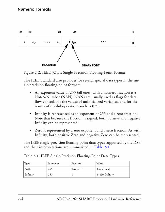
Numeric Formats
2-4 ADSP-2126x SHARC Processor Hardware Reference
The IEEE Standard also provides for several special data types in the sin-gle-precision floating-point format:
• An exponent value of 255 (all ones) with a nonzero fraction is a Not-A-Number (NAN). NANs are usually used as flags for data flow control, for the values of uninitialized variables, and for the results of invalid operations such as 0 * ∞.
• Infinity is represented as an exponent of 255 and a zero fraction. Note that because the fraction is signed, both positive and negative Infinity can be represented.
• Zero is represented by a zero exponent and a zero fraction. As with Infinity, both positive Zero and negative Zero can be represented.
The IEEE single-precision floating-point data types supported by the DSP and their interpretations are summarized in Table 2-1.
Figure 2-2. IEEE 32-Bit Single-Precision Floating-Point Format
Table 2-1. IEEE Single-Precision Floating-Point Data Types
Type Exponent Fraction Value
NAN 255 Nonzero Undefined
Infinity 255 0 (–1)σ Infinity
s e0
31 30 23 22 0
1 . f22 f0e7 • • •
HIDDEN BIT BINARY POINT
• • •

ADSP-2126x SHARC Processor Hardware Reference 2-5
Processing Elements
Extended-precision Floating-Point FormatThe extended-precision floating-point format is 40 bits wide, with the same 8-bit exponent as in the IEEE Standard format but a 32-bit signifi-cand. This format is shown in Figure 2-3. In all other respects, the extended-precision floating-point format is the same as the IEEE Standard format.
Short Word Floating-Point FormatThe DSP supports a 16-bit floating-point data type and provides conver-sion instructions for it. The short float data format has an 11-bit mantissa with a 4-bit exponent plus sign bit, as shown in Figure 2-4. The 16-bit floating-point numbers reside in the lower 16 bits of the 32-bit float-ing-point field.
Normal 1 ≤ e ≤ 254 Any (–1)σ (1.f22-0) 2 e–127
Zero 0 0 (–1)σ Zero
Figure 2-3. 40-Bit Extended-Precision Floating-Point Format
Table 2-1. IEEE Single-Precision Floating-Point Data Types (Cont’d)
Type Exponent Fraction Value
s e0
39 38 31 30 0
1 . f30 f0e7 • • • • • •
HIDDEN BIT BINARY POINT

Numeric Formats
2-6 ADSP-2126x SHARC Processor Hardware Reference
Packing for Floating-Point DataTwo shifter instructions, FPACK and FUNPACK, perform the packing and unpacking conversions between 32-bit floating-point words and 16-bit floating-point words. The FPACK instruction converts a 32-bit IEEE float-ing-point number to a 16-bit floating-point number. The FUNPACK instruction converts the 16-bit floating-point numbers back to 32-bit IEEE floating-point numbers. Each instruction executes in a single cycle. The results of the FPACK and FUNPACK operations appear in Table 2-2 and Table 2-3.
Figure 2-4. 16-Bit Floating-Point Format
Table 2-2. FPACK Operations
Condition Result
135 < exp Largest magnitude representation.
120 < exp ≤ 135 Exponent is Most Significant Bit (MSB) of source exponent concatenated with the three Least Significant Bits (LSBs) of source exponent. The packed fraction is the rounded upper 11 bits of the source fraction.
109 < exp ≤ 120 Exponent = 0. Packed fraction is the upper bits (source exponent – 110) of the source fraction prefixed by zeros and the “hidden” one. The packed fraction is rounded.
exp < 110 Packed word is all zeros.
exp = source exponentsign bit remains the same in all cases
s e0
15 14 11 10 0
1 . f10 f0e3 • • • • • •
HIDDEN BIT BINARY POINT
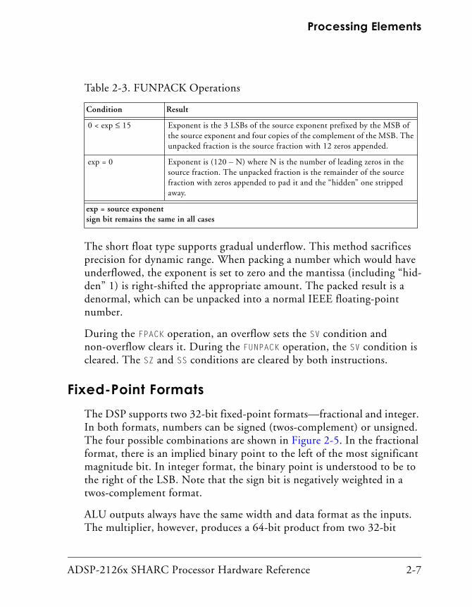
ADSP-2126x SHARC Processor Hardware Reference 2-7
Processing Elements
The short float type supports gradual underflow. This method sacrifices precision for dynamic range. When packing a number which would have underflowed, the exponent is set to zero and the mantissa (including “hid-den” 1) is right-shifted the appropriate amount. The packed result is a denormal, which can be unpacked into a normal IEEE floating-point number.
During the FPACK operation, an overflow sets the SV condition and non-overflow clears it. During the FUNPACK operation, the SV condition is cleared. The SZ and SS conditions are cleared by both instructions.
Fixed-Point FormatsThe DSP supports two 32-bit fixed-point formats—fractional and integer. In both formats, numbers can be signed (twos-complement) or unsigned. The four possible combinations are shown in Figure 2-5. In the fractional format, there is an implied binary point to the left of the most significant magnitude bit. In integer format, the binary point is understood to be to the right of the LSB. Note that the sign bit is negatively weighted in a twos-complement format.
ALU outputs always have the same width and data format as the inputs. The multiplier, however, produces a 64-bit product from two 32-bit
Table 2-3. FUNPACK Operations
Condition Result
0 < exp ≤ 15 Exponent is the 3 LSBs of the source exponent prefixed by the MSB of the source exponent and four copies of the complement of the MSB. The unpacked fraction is the source fraction with 12 zeros appended.
exp = 0 Exponent is (120 – N) where N is the number of leading zeros in the source fraction. The unpacked fraction is the remainder of the source fraction with zeros appended to pad it and the “hidden” one stripped away.
exp = source exponentsign bit remains the same in all cases

Numeric Formats
2-8 ADSP-2126x SHARC Processor Hardware Reference
inputs. If both operands are unsigned integers, the result is a 64-bit unsigned integer. If both operands are unsigned fractions, the result is a 64-bit unsigned fraction. These formats are shown in Figure 2-7.
If one operand is signed and the other unsigned, the result is signed. If both inputs are signed, the result is signed and automatically shifted left one bit. The LSB becomes zero and bit 62 moves into the sign bit posi-tion. Normally bit 63 and bit 62 are identical when both operands are signed. (The only exception is full-scale negative multiplied by itself.) Thus, the left-shift normally removes a redundant sign bit, increasing the precision of the most significant product. Also, if the data format is frac-tional, a single bit left-shift renormalizes the MSP to a fractional format. The signed formats with and without left-shifting are shown in Figure 2-6.
The multiplier has an 80-bit accumulator to allow the accumulation of 64-bit products. For more information on the multiplier and accumula-tor, see “Multiply Accumulator (Multiplier)” on page 2-22.

ADSP-2126x SHARC Processor Hardware Reference 2-9
Processing Elements
Figure 2-5. 32-Bit Fixed-Point Formats
31 30 29
• • •
2 1
-2 31 2 30 2 29 22 21 20
S IG NB IT
W E IG H T
B IT
B IN A R Y P O IN T
0
31 30 2 9
• • •
2 1
2 -29W E IG H T
B IT
B IN A R Y P O IN T
0
2 -3 0 2 -31-2 -0 2 -1 2-2
S IG N
B IT
S IG N E D FR A C TIO N A L
S IG N E D IN TE G E R
• • • 2 -3 0 2 -31 2 -32•2 -1 2 -2 2 -3
U N S IG N E D IN TE G E R
U N S IG N ED FR A C TIO N A L
•
•
B IN A R Y PO IN T
3 1 3 0 29
• • •
2 1
2 31 2 30 229 22 21 20•
W E IG H T
B IT 0
31 30 2 9 2 1
W E IG H T
B IT
B IN A R Y P O IN T
0

Numeric Formats
2-10 ADSP-2126x SHARC Processor Hardware Reference
Figure 2-6. 64-Bit Signed Fixed-Point Product
Figure 2-7. 64-Bit Unsigned Fixed-Point Product
63 62 61
• • •
2 1
SIGNBIT
WEIGHT
BIT 0
SIGNED INTEGER, NO LEFT SHIFT
-263 262 261 22 21 20• • ••
BINARYPOINT
SIGNED FRACTIONAL, WITH LEFT SHIFT
63 62 61
• • •
2 1
2-61
0
2-62 2-63-20 2-1 2-2•
BINARYPOINT
SIGNBIT
WEIGHT
BIT
63 62 61
• • •
2 1
WEIGHT
BIT 0
SIGNED INTEGER
263 262 261 22 21 20•
BINARYPOINT
SIGNED FRACTIONAL
63 62 61
• • •
2 1
2-62
0
2-63 2-642-1 2-2 2-3•
BINARYPOINT
WEIGHT
BIT

ADSP-2126x SHARC Processor Hardware Reference 2-11
Processing Elements
Setting Computational ModesThe MODE1 register controls the operating mode of the processing ele-ments. Table A-2 on page A-5 lists all the bits in MODE1. The following bits in MODE1 control computational modes:
• Floating-point data format. Bit 16 (RND32) directs the computa-tional units to round floating-point data to 32 bits (if 1) or round to 40 bits (if 0).
• Rounding mode. Bit 15 (TRUNC) directs the computational units to round results with round-to-zero (if 1) or round-to-nearest (if 0).
• ALU saturation. Bit 13 (ALUSAT) directs the computational units to saturate results on positive or negative fixed-point overflows (if 1) or return unsaturated results (if 0).
• Short word sign extension. Bit 14 (SSE) directs the computational units to sign extended short word 16-bit data (if 1) or zero-fill the upper 16 bits (if 0).
• Secondary processor element (PEy). Bit 21 (PEYEN) enables compu-tations in PEy (SIMD mode) (if 1) or disables PEy Single Instruction Single Data (SISD mode) (if 0).
32-Bit Floating-Point Format (Normal Word)In the default mode of the DSP (RND32 bit=1), the multiplier and ALU support a single-precision floating-point format, which is specified in the IEEE 754/854 standard. For more information on this standard, see

Setting Computational Modes
2-12 ADSP-2126x SHARC Processor Hardware Reference
“Numeric Formats” on page 2-3. This format is IEEE 754/854 compati-ble for single-precision floating-point operations in all respects except:
• The DSP does not provide inexact flags. An inexact flag is an exception flag whose bit position is inexact. The inexact exception occurs if the rounded result of an operation is not identical to the exact (infinitely precise) result. Thus, an inexact exception always occurs when an overflow or an underflow occurs.
• NAN (Not-A-Number) inputs generate an invalid exception and return a quiet NAN (all 1s).
• Denormal operands, using denormalized (or tiny) numbers, flush to zero when input to a computational unit and do not generate an underflow exception. A denormal operand is one of the float-ing-point operands with an absolute value too small to represent with full precision in the significant. The denormal exception occurs if one or more of the operands is a denormal number. This exception is never regarded as an error.
• The processor supports round-to-nearest and round-toward-zero modes, but does not support round-to-+Infinity and round-to --Infinity.
IEEE single-precision floating-point data uses a 23-bit mantissa with an 8-bit exponent plus sign bit. In this case, the computation unit sets the eight LSBs of floating-point inputs to zeros before performing the opera-tion. The mantissa of a result rounds to 23 bits (not including the hidden bit), and the 8 LSBs of the 40-bit result clear to zeros to form a 32-bit number, which is equivalent to the IEEE standard result.
In fixed-point to floating-point conversion, the rounding boundary is always 40 bits, even if the RND32 bit is set.
ADSP-2126x SHARC Processor Hardware Reference 2-13
Processing Elements
40-Bit Floating-Point FormatWhen in extended-precision mode (RND32 bit=0), the DSP supports a 40-bit extended-precision floating-point mode, which has eight additional LSBs of the mantissa and is compliant with the 754/854 standards. How-ever, results in this format are more precise than the IEEE single-precision standard specifies. Extended-precision floating-point data uses a 31-bit mantissa with a 8-bit exponent plus sign bit.
16-Bit Floating-Point Format (Short Word)The DSP supports a 16-bit floating-point storage format and provides instructions that convert the data for 40-bit computations. The 16-bit floating-point format uses an 11-bit mantissa with a 4-bit exponent plus sign bit. The 16-bit data goes into bits 23 through 8 of a data register. Two shifter instructions, Fpack and Funpack, perform the packing and unpacking conversions between 32-bit floating-point words and 16-bit floating-point words. The Fpack instruction converts a 32-bit IEEE float-ing-point number in a data register into a 16-bit floating-point number. Funpack converts a 16-bit floating-point number in a data register to a 32-bit IEEE floating-point number. Each instruction executes in a single cycle.
When 16-bit data is written to bits 23 through 8 of a data register, the DSP automatically extends the data into a 32-bit integer (bits 39 through 8). If the SSE bit in MODE1 is set (1), the DSP sign extends the upper 16 bits. If the SSE bit is cleared (0), the DSP zeros the upper 16 bits.
The 16-bit floating-point format supports gradual underflow. This method sacrifices precision for dynamic range. When packing a number that would have underflowed, the exponent clears to zero and the mantissa (including a “hidden” 1) right-shifts the appropriate amount. The packed result is a denormal, which can be unpacked into a normal IEEE float-ing-point number.

Setting Computational Modes
2-14 ADSP-2126x SHARC Processor Hardware Reference
32-Bit Fixed-Point FormatThe DSP always represents fixed-point numbers in 32 bits, occupying the 32 MSBs in 40-bit data registers. Fixed-point data may be fractional or integer numbers and unsigned or twos-complement. Each computational unit has its own limitations on how these formats may be mixed for a given operation. All computational units read the upper 32 bits of data (inputs, operands) from the 40-bit registers (ignoring the eight LSBs) and write results to the upper 32 bits (zeroing the eight LSBs).
Rounding ModeThe TRUNC bit in the MODE1 register determines the rounding mode for all ALU operations, all floating-point multiplies, and fixed-point multiplies of fractional data. The DSP supports two modes of rounding: round-toward-zero and round-toward-nearest. The rounding modes com-ply with the IEEE 754 standard and have the following definitions:
• Round-toward-zero (TRUNC bit=1). If the result before rounding is not exactly representable in the destination format, the rounded result is the number that is nearer to zero. This is equivalent to truncation.
• Round-toward-nearest (TRUNC bit=0). If the result before rounding is not exactly representable in the destination format, the rounded result is the number that is nearer to the result before rounding. If the result before rounding is exactly halfway between two numbers in the destination format (differing by an LSB), the rounded result is the number that has an LSB equal to zero.
Statistically, rounding up occurs as often as rounding down, so there is no large sample bias. Because the maximum floating-point value is one LSB less than the value that represents infinity, a result that is halfway between the maximum floating-point value and Infinity rounds to Infinity in this mode.

ADSP-2126x SHARC Processor Hardware Reference 2-15
Processing Elements
Though these rounding modes comply with standards set for float-ing-point data, they also apply for fixed-point multiplier operations on fractional data. The same two rounding modes are supported, but only the round-to-nearest operation is actually performed by the multiplier. Using its local result register for fixed-point operations, the multiplier rounds-to-zero by reading only the upper bits of the result and discarding the lower bits.
Using Computational StatusThe multiplier and ALU each provide exception information when exe-cuting floating-point operations. Each unit updates overflow, underflow, and invalid operation flags in the processing element’s arithmetic status (ASTATx and ASTATy) registers and sticky status (STKYx and STKYy) registers. An underflow, overflow, or invalid operation from any unit also generates a maskable interrupt. There are three ways to use floating-point excep-tions from computations in program sequencing:
• Interrupts. Enable interrupts and use an interrupt service routine (ISR) to handle the exception condition immediately. This method is appropriate if it is important to correct all exceptions as they occur.
• The ASTATx and ASTATy registers. Use conditional instructions to test the exception flags in the ASTATx or ASTATy registers after the instruction executes. This method permits monitoring each instruction’s outcome.
• The STKYx and STKYy registers. Use the bit test (BTST) instruction to examine exception flags in the STKY register after a series of oper-ations. If any flags are set, some of the results are incorrect. This method is useful when exception handling is not critical.

Arithmetic Logic Unit (ALU)
2-16 ADSP-2126x SHARC Processor Hardware Reference
More information on ASTAT and STKY status appears in the sections that describe the computational units. For summaries relating instructions and status bits, see Table 2-4, Table 2-5, Table 2-6, Table 2-7, and Table 2-8.
Arithmetic Logic Unit (ALU)The ALU performs arithmetic operations on fixed-point or floating-point data and logical operations on fixed-point data. ALU fixed-point instruc-tions operate on 32-bit fixed-point operands and output 32-bit fixed-point results, while ALU floating-point instructions operate on 32-bit or 40-bit floating-point operands and output 32-bit or 40-bit float-ing-point results. ALU instructions include:
• Floating-point addition, subtraction, add/subtract, average
• Fixed-point addition, subtraction, add/subtract, average
• Floating-point manipulation: binary log, scale, mantissa
• Fixed-point add with carry, subtract with borrow, increment, decrement
• Logical And, Or, Xor, Not
• Functions: Abs, pass, min, max, clip, compare
• Format conversion
• Reciprocal and reciprocal square root primitives
ALU OperationALU instructions take one or two inputs: X input and Y input. These inputs (also known as operands) can be any data registers in the register file. Most ALU operations return one result; in add/subtract operations, the ALU operation returns two results, and in compare operations, the

ADSP-2126x SHARC Processor Hardware Reference 2-17
Processing Elements
ALU operation returns no result (only flags are updated). ALU results can be returned to any location in the register file.
The DSP transfers input operands from the register file during the first half of the processor cycle and transfers results to the register file during the second half of the cycle. With this arrangement, the ALU can read and write the same register file location in a single cycle. If the ALU operation is fixed-point, the inputs are treated as 32-bit fixed-point operands. The ALU transfers the upper 32 bits from the source location in the register file. For fixed-point operations, the result(s) are always 32-bit fixed-point values. Some floating-point operations (Logb, Mant and Fix) can also yield fixed-point results.
The DSP transfers fixed-point results to the upper 32 bits of the data reg-ister and clears the lower eight bits of the register. The format of fixed-point operands and results depends on the operation. In most arith-metic operations, there is no need to distinguish between integer and fractional formats. Fixed-point inputs to operations such as scaling a float-ing-point value are treated as integers. For purposes of determining status such as overflow, fixed-point arithmetic operands and results are treated as twos-complement numbers.
ALU SaturationWhen the ALUSAT bit is set (=1) in the MODE1 register, the ALU is in satura-tion mode. In this mode, all positive fixed-point overflows return the maximum positive fixed-point number (0x7FFF FFFF), and all negative overflows return the maximum negative number (0x8000 0000).
When the ALUSAT bit is cleared (=0) in the MODE1 register, fixed-point results that overflow are not saturated; the upper 32 bits of the result are returned unaltered.
The ALU overflow flag reflects the ALU result before saturation.

Arithmetic Logic Unit (ALU)
2-18 ADSP-2126x SHARC Processor Hardware Reference
ALU Status FlagsALU operations update seven status flags in the processing element’s arith-metic status (ASTATx and ASTATy) registers. Table A-4 on page A-12 lists all the bits in these registers. The following bits in ASTATx or ASTATy flag the ALU status (a 1 indicates the condition) of the most recent ALU operation:
• ALU result zero or floating-point underflow. Bit 0 (AZ)
• ALU overflow. Bit 1 (AV)
• ALU result negative. Bit 2 (AN)
• ALU fixed-point carry. Bit 3 (AC)
• ALU X input sign for Abs, Mant operations. Bit 4 (AS)
• ALU floating-point invalid operation. Bit 5 (AI)
• Last ALU operation was a floating-point operation. Bit 10 (AF)
• Compare Accumulation register results of last eight compare opera-tions. Bits 31-24 (CACC)
ALU operations also update four “sticky” status flags in the processing ele-ment’s sticky status (STKYx and STKYy) registers. Table A-5 on page A-17 lists all the bits in these registers. The following bits in STKYx or STKYy flag the ALU status (a 1 indicates the condition). Once set, a sticky flag remains high until explicitly cleared:
• ALU floating-point underflow. Bit 0 (AUS)
• ALU floating-point overflow. Bit 1 (AVS)
• ALU fixed-point overflow. Bit 2 (AOS)
• ALU floating-point invalid operation. Bit 5 (AIS)

ADSP-2126x SHARC Processor Hardware Reference 2-19
Processing Elements
Flag updates occur at the end of the cycle in which the status is generated and is available on the next cycle. If a program writes the arithmetic status register or sticky status register explicitly in the same cycle that the ALU is performing an operation, the explicit write to the status register supersedes any flag update from the ALU operation.
ALU Instruction SummaryTable 2-4 and Table 2-5 list the ALU instructions and show how they relate to ASTATx,y and STKYx,y flags. For more information on assembly language syntax, see the SHARC Processor Programming Reference. In these tables, note the meaning of these symbols:
• Rn, Rx, Ry indicate any register file location; treated as fixed-point
• Fn, Fx, Fy indicate any register file location; treated as floating-point
• * indicates the flag may be set or cleared, depending on the results of instruction
• ** indicates the flag may be set (but not cleared), depending on the results of the instruction
• – indicates no effect

Arithmetic Logic Unit (ALU)
2-20 ADSP-2126x SHARC Processor Hardware Reference
Table 2-4. Fixed-Point ALU Instruction Summary
Instruction ASTATx,y Status Flags STKYx,y Status Flags
Fixed-point: AZ
AV AN
AC
AS AI AF CACC
AUS
AVS
AOS
AIS
Rn = Rx + Ry * * * * 0 0 0 – – – ** –
Rn = Rx – Ry * * * * 0 0 0 – – – ** –
Rn = Rx + Ry + CI * * * * 0 0 0 – – – ** –
Rn = Rx – Ry + CI – 1 * * * * 0 0 0 – – – ** –
Rn = (Rx + Ry)/2 * 0 * * 0 0 0 – – – – –
COMP(Rx, Ry) * 0 * 0 0 0 0 * – – – –
COMPU(Rx,Ry) * 0 * 0 0 0 0 * -- -- -- --
Rn = Rx + CI * * * * 0 0 0 – – – ** –
Rn = Rx + CI – 1 * * * * 0 0 0 – – – ** –
Rn = Rx + 1 * * * * 0 0 0 – – – ** –
Rn = Rx – 1 * * * * 0 0 0 – – – ** –
Rn = –Rx * * * * 0 0 0 – – – ** –
Rn = ABS Rx * * 0 0 * 0 0 – – – ** –
Rn = PASS Rx * 0 * 0 0 0 0 – – – – –
Rn = Rx AND Ry * 0 * 0 0 0 0 – – – – –
Rn = Rx OR Ry * 0 * 0 0 0 0 – – – – –
Rn = Rx XOR Ry * 0 * 0 0 0 0 – – – – –
Rn = NOT Rx * 0 * 0 0 0 0 – – – – –
Rn = MIN(Rx, Ry) * 0 * 0 0 0 0 – – – – –
Rn = MAX(Rx, Ry) * 0 * 0 0 0 0 – – – – –
Rn = CLIP Rx BY Ry * 0 * 0 0 0 0 – – – – –

ADSP-2126x SHARC Processor Hardware Reference 2-21
Processing Elements
Table 2-5. Floating-Point ALU Instruction Summary
Instruction ASTATx,y Status Flags STKYx,y Status Flags
Floating-point: AZ AV AN AC AS AI AF CACC
AUS
AVS
AOS
AIS
Fn = Fx + Fy * * * 0 0 * 1 – ** ** – **
Fn = Fx – Fy * * * 0 0 * 1 – ** ** – **
Fn = ABS (Fx + Fy) * * 0 0 0 * 1 – ** ** – **
Fn = ABS (Fx – Fy) * * 0 0 0 * 1 – ** ** – **
Fn = (Fx + Fy)/2 * 0 * 0 0 * 1 – ** – – **
COMP(Fx, Fy) * 0 * 0 0 * 1 * – – – **
Fn = –Fx * * * 0 0 * 1 – – ** – **
Fn = ABS Fx * * 0 0 * * 1 – – ** – **
Fn = PASS Fx * 0 * 0 0 * 1 – – – – **
Fn = RND Fx * * * 0 0 * 1 – – ** – **
Fn = SCALB Fx BY Ry * * * 0 0 * 1 – ** ** – **
Rn = MANT Fx * * 0 0 * * 1 – – ** – **
Rn = LOGB Fx * * * 0 0 * 1 – – ** – **
Rn = FIX Fx BY Ry * * * 0 0 * 1 – ** ** – **
Rn = FIX Fx * * * 0 0 * 1 – ** ** – **
Fn = FLOAT Rx BY Ry * * * 0 0 0 1 – ** ** – –
Fn = FLOAT Rx * 0 * 0 0 0 1 – – – – –
Fn = RECIPS Fx * * * 0 0 * 1 – ** ** – **
Fn = RSQRTS Fx * * * 0 0 * 1 – – ** – **
Fn = Fx COPYSIGN Fy * 0 * 0 0 * 1 – – – – **
Fn = MIN(Fx, Fy) * 0 * 0 0 * 1 – – – – **
Fn = MAX(Fx, Fy) * 0 * 0 0 * 1 – – – – **
Fn = CLIP Fx BY Fy * 0 * 0 0 * 1 – – – – **

Multiply Accumulator (Multiplier)
2-22 ADSP-2126x SHARC Processor Hardware Reference
Multiply Accumulator (Multiplier)The multiplier performs fixed-point or floating-point multiplication and fixed-point multiply/accumulate operations. Fixed-point multiply/accu-mulates are available with either cumulative addition or cumulative subtraction. Multiplier floating-point instructions operate on 32-bit or 40-bit floating-point operands and output 32-bit or 40-bit floating-point results. Multiplier fixed-point instructions operate on 32-bit fixed-point data and produce 80-bit results. Inputs are treated as fractional or integer, unsigned or twos-complement. Multiplier instructions include:
• Floating-point multiplication
• Fixed-point multiplication
• Fixed-point multiply/accumulate with addition, rounding optional
• Fixed-point multiply/accumulate with subtraction, rounding optional
• Rounding result register
• Saturating result register
• Clearing result register
Multiplier OperationThe multiplier takes two inputs: X input and Y input. These inputs (also known as operands) can be any data registers in the register file. The multiplier can accumulate fixed-point results in the local Multiplier Result (MRF) registers or write results back to the register file. The results in MRF can also be rounded or saturated in separate operations. Floating-point multiplies yield floating-point results, which the multiplier always writes directly to the register file.

ADSP-2126x SHARC Processor Hardware Reference 2-23
Processing Elements
The multiplier transfers input operands during the first half of the proces-sor cycle and transfers results during the second half of the cycle. With this arrangement, the multiplier can read and write the same register file location in a single cycle.
For fixed-point multiplies, the multiplier reads the inputs from the upper 32 bits of the data registers. Fixed-point operands may be either both in integer format or both in fractional format. The format of the result matches the format of the inputs. Each fixed-point operand may be either an unsigned or a twos-complement number. If both inputs are fractional and signed, the multiplier automatically shifts the result left one bit to remove the redundant sign bit. The register name(s) within the multiplier instruction specify input data type(s)—Fx for floating-point and Rx for fixed-point.
Multiplier Result Register (Fixed-Point)Fixed-point operations place 80-bit results in the multiplier’s foreground MRF register or background MRB register, depending on which is active. For more information on selecting the result register, see “Alternate (Second-ary) Data Registers” on page 2-39.
The location of a result in the MRF register’s 80-bit field depends on whether the result is in fractional or integer format, as shown in Figure 2-8. If the result is sent directly to a data register, the 32-bit result with the same format as the input data is transferred, using bits 63-32 for a fractional result or bits 31-0 for an integer result. The eight LSBs of the 40-bit register file location are zero-filled.
Fractional results can be rounded-to-nearest before being sent to the regis-ter file. If rounding is not specified, discarding bits 31-0 effectively truncates a fractional result (rounds to zero). For more information on rounding, see “Rounding Mode” on page 2-14.
Multiply Accumulator (Multiplier)
2-24 ADSP-2126x SHARC Processor Hardware Reference
The MRF register is divided into MRF2, MRF1, and MRF0 registers, which can be individually read from or written to the register file. Each of these reg-isters has the same format. When data is read from MRF2, it is sign-extended to 32 bits as shown in Figure 2-9. The DSP zero-fills the eight LSBs of the 40-bit register file location when data is read from MRF2, MRF1, or MRF0 to the register file. When the DSP writes data into MRF2, MRF1, or MRF0 from the 32 MSBs of a register file location, the eight LSBs are ignored. Data written to MRF1 is sign-extended to MRF2, repeating the MSB of MRF1 in the 16 bits of MRF2. Data written to MRF0 is not sign-extended.
Figure 2-8. Multiplier Fixed-Point Result Placement
Figure 2-9. MR Transfer Formats
MRF2 MRF0
OVERFLOW UNDERFLOWFRACTIONAL RESULT
OVERFLOW INTEGER RESULTOVERFLOW
MRF1
79 63 31 0
ZEROSSIGN-EXTEND MRF2
MRF0
MRF1
16 BITS 16 BITS
8 BITS32 BITS
ZEROS
ZEROS
8 BITS32 BITS
8 BITS

ADSP-2126x SHARC Processor Hardware Reference 2-25
Processing Elements
In addition to multiplication, fixed-point operations include accumula-tion, rounding, and saturation of fixed-point data. There are three MRF register operations: clear (Clr), round (Rnd), and saturate (Sat).
The Clr operation (MRF=0) resets the specified MRF register to zero. Often, it is best to perform this operation at the start of a multiply/accumulate operation to remove results left over from the previous operation.
The Rnd operation (MRF=Rnd MRF) applies only to fractional results, so inte-ger results are not effected. This operation rounds the 80-bit MRF value to nearest at bit 32; for example, the MRF1-MRF0 boundary. Rounding of a fixed-point result occurs either as part of a multiply or multiply/accumu-late operation or as an explicit operation on the MRF register. The rounded result in MRF1 can be sent either to the register file or back to the same MRF register. To round a fractional result to zero (truncation) instead of to nearest, a program transfers the unrounded result from MRF1, discarding the lower 32 bits in MRF0.
The Sat operation (MRF=Sat MRF) sets MRF to a maximum value if the MRF value has overflowed. Overflow occurs when the MRF value is greater than the maximum value for the data format—unsigned or twos-complement and integer or fractional—as specified in the saturate instruction. The six possible maximum values appear in Table 2-6. The result from MRF satura-tion can be sent either to the register file or back to the same MRF register.
Table 2-6. Fixed-Point Format Maximum Values (For Saturation)
Maximum Number (Hexadecimal)
MRF2 MRF1 MRF0
Two’s-complement fractional (positive) 0000 7FFF FFFF FFFF FFFF
Two’s-complement fractional (negative) FFFF 8000 0000 0000 0000
Two’s-complement integer (positive) 0000 0000 0000 7FFF FFFF
Two’s-complement integer (negative) FFFF FFFF FFFF 8000 0000

Multiply Accumulator (Multiplier)
2-26 ADSP-2126x SHARC Processor Hardware Reference
Multiplier Status FlagsMultiplier operations update four status flags in the processing element’s arithmetic status registers (ASTATx and ASTATy). “Arithmetic Status Regis-ters (ASTATx and ASTATy)” on page A-10 lists all the bits in these registers. The following bits in the ASTATx or ASTATy registers flag the mul-tiplier status (a 1 indicates the condition) of the most recent multiplier operation:
• Multiplier result negative. Bit 6 (MN)
• Multiplier overflow. Bit 7 (MV)
• Multiplier underflow. Bit 8 (MU)
• Multiplier floating-point invalid operation. Bit 9 (MI)
Multiplier operations also update four “sticky” status flags in the process-ing element’s sticky status (STKYx and STKYy) registers. The following bits in the STKYx or STKYy flag multiplier status (a 1 indicates the condition). Once set, a sticky flag remains high until explicitly cleared:
• Multiplier fixed-point overflow. Bit 6 (MOS)
• Multiplier floating-point overflow. Bit 7 (MVS)
• Multiplier underflow. Bit 8 (MUS)
• Multiplier floating-point invalid operation. Bit 9 (MIS)
Unsigned fractional number 0000 FFFF FFFF FFFF FFFF
Unsigned integer number 0000 0000 0000 FFFF FFFF
Table 2-6. Fixed-Point Format Maximum Values (For Saturation) (Cont’d)
Maximum Number (Hexadecimal)
MRF2 MRF1 MRF0

ADSP-2126x SHARC Processor Hardware Reference 2-27
Processing Elements
Flag updates occur at the end of the cycle in which the status is generated and is available on the next cycle. If a program writes the arithmetic status register or sticky register explicitly in the same cycle that the multiplier is performing an operation, the explicit write to ASTAT or STKY supersedes any flag update from the multiplier operation.
Multiplier Instruction SummaryTable 2-7 and Table 2-9 list the Multiplier instructions and describe how they relate to ASTATx,y and STKYx,y flags. For more information on assembly language syntax, see the SHARC Processor Programming Refer-ence. In these tables, note the meaning of the following symbols:
• Rn, Rx, Ry indicate any register file location; treated as fixed-point
• Fn, Fx, Fy indicate any register file location; treated as floating-point
• * indicates the flag may be set or cleared, depending on results of instruction
• ** indicates the flag may be set (but not cleared), depending on results of instruction
• – indicates no effect
• The Input Mods column indicates the types of optional modifiers that can be applied to the instruction inputs. For a list of modifiers, see Table 2-8.
Multiply Accumulator (Multiplier)
2-28 ADSP-2126x SHARC Processor Hardware Reference
Table 2-7. Fixed-Point Multiplier Instruction Summary
Instruction Input Mods
ASTATx,y Flags STKYx,y Flags
Fixed-Point:For Input Mods, see Table 2-8
MU MN MV MI MUS MOS MVS MIS
Rn = Rx * Ry 1 * * * 0 – ** – –
MRF = Rx * Ry 1 * * * 0 – ** – –
MRB = Rx * Ry 1 * * * 0 – ** – –
Rn = MRF + Rx * Ry 1 * * * 0 – ** – –
Rn = MRB + Rx * Ry 1 * * * 0 – ** – –
MRF = MRF + Rx * Ry 1 * * * 0 – ** – –
MRB = MRB + Rx * Ry 1 * * * 0 – ** – –
Rn = MRF – Rx * Ry 1 * * * 0 – ** – –
Rn = MRB – Rx * Ry 1 * * * 0 – ** – –
MRF = MRF – Rx * Ry 1 * * * 0 – ** – –
MRB = MRB – Rx * Ry 1 * * * 0 – ** – –
Rn = SAT MRF 2 * * * 0 – ** – –
Rn = SAT MRB 2 * * * 0 – ** – –
MRF = SAT MRF 2 * * * 0 – ** – –
MRB = SAT MRB 2 * * * 0 – ** – –
Rn = RND MRF 3 * * * 0 – ** – –
Rn = RND MRB 3 * * * 0 – ** – –
MRF = RND MRF 3 * * * 0 – ** – –
MRB = RND MRB 3 * * * 0 – ** – –
MRF = 0 – 0 0 0 0 – – – –
MRB = 0 – 0 0 0 0 – – – –
MRxF = Rn – 0 0 0 0 – – – –
MRxB = Rn – 0 0 0 0 – – – –
Rn = MRxF – 0 0 0 0 – – – –
Rn = MRxB – 0 0 0 0 – – – –

ADSP-2126x SHARC Processor Hardware Reference 2-29
Processing Elements
Barrel Shifter (Shifter)The shifter performs bit-wise operations on 32-bit fixed-point operands. Shifter operations include:
• Shifts and rotates from off-scale left to off-scale right
• Bit manipulation operations, including bit set, clear, toggle, and test
Table 2-8. Input Modifiers For Fixed-Point Multiplier Instruction
InputMods from Table 2-7
Input Mods—Options For Fixed-Point Multiplier Instructions
Note the meaning of the following symbols in this table:Signed inputS
Unsigned inputU
Integer inputI
Fractional inputF
Fractional inputs, Rounded outputFR Note that (SF) is the default format for one-input operations, and (SSF) is the default format for two-input operations.
1 (SSF), (SSI), (SSFR), (SUF), (SUI), (SUFR), (USF), (USI), (USFR), (UUF), (UUI), or (UUFR)
2 (SF), (SI), (UF), or (UI)
3 (SF) or (UF)
Table 2-9. Floating-Point Multiplier Instruction Summary
Instruction ASTATx,y Flags STKYx,y Flags
Floating-Point: MU MN MV MI MUS MOS MVS MIS
Fn = Fx * Fy * * * * ** – ** **

Barrel Shifter (Shifter)
2-30 ADSP-2126x SHARC Processor Hardware Reference
• Bit field manipulation operations, including extract and deposit
• Fixed-point/floating-point conversion operations, including expo-nent extract, number of leading 1s or 0s
Shifter OperationThe shifter takes from one to three inputs: X input, Y input, and Z input. The inputs (also known as operands) can be any register in the register file. Within a shifter instruction, the inputs serve as follows.
• The X input provides data that is operated on.
• The Y input specifies shift magnitudes, bit field lengths, or bit positions.
• The Z input provides data that is operated on and updated.
In the following example, Rx is the X input, Ry is the Y input, and Rn is the Z input. The shifter returns one output (Rn) to the register file.
Rn = Rn OR LSHIFT Rx BY Ry;
As shown in Figure 2-9, the shifter fetches input operands from the upper 32 bits of a register file location (bits 39-8) or from an immediate value in the instruction. The shifter transfers operands during the first half of the cycle and transfers the result to the upper 32 bits of a register (with the eight LSBs zero-filled) during the second half of the cycle. With this arrangement, the shifter can read and write the same register file location in a single cycle.
The X input and Z input are always 32-bit fixed-point values. The Y input is a 32-bit fixed-point value or an 8-bit field (shf8), positioned in the reg-ister file. These inputs appear in Figure 2-9.
Some shifter operations produce 8-bit or 6-bit results. As shown in Figure 2-10, the shifter places these results in either the shf8 field or the

ADSP-2126x SHARC Processor Hardware Reference 2-31
Processing Elements
bit6 field and sign-extends the results to 32 bits. The shifter always returns a 32-bit result.
The shifter supports bit field deposit and bit field extract instructions for manipulating groups of bits within an input. The Y input for bit field instructions specifies two 6-bit values: bit6 and len6, which are positioned in the Ry register as shown in Figure 2-10. The shifter interprets bit6 and len6 as positive integers. Bit6 is the starting bit position for the deposit or extract, and len6 is the bit field length, which specifies how many bits are deposited or extracted.
Field deposit (Fdep) instructions take a group of bits from the input regis-ter (starting at the LSB of the 32-bit integer field) and deposit the bits as directed anywhere within the result register. The bit6 value specifies the starting bit position for the deposit. Figure 2-11 shows how the inputs, bit6 and len6, work in a field deposit instruction:
Rn = FDEP Rx By Ry
Figure 2-10. Register File Fields for Shifter Instructions
Figure 2-11. Register File Fields for FDEP, FEXT Instructions
39 7 0
32-BIT Y INPUT OR RESULT
39 15 7 0
SHF8
8-BIT Y INPUT OR RESULT
39 19 13 7 0
LEN6 BIT6
12-BIT Y INPUT

Barrel Shifter (Shifter)
2-32 ADSP-2126x SHARC Processor Hardware Reference
Figure 2-12 shows bit placement for the following field deposit instruction:
R0 = FDEP R1 BY R2;
Figure 2-12. Bit Field Deposit Instruction
00000000111111110000000000000000
39 32 24 16
16
8
8
0
0
0X0000 00FF 00R1 00000000
00000000 00000000000100000000001000000000
39 32 24 16 8 0
LEN6 BIT6 LEN6 = 8BIT6 = 16
0X0000 0210 00R2
00000000 0000000000000000
39 32 24 16 8 0
16 8 0
STARTING BIT POSITIONFOR DEPOSIT
REFERENCE POINT
0X00FF 0000 00R0 11111111 00000000

ADSP-2126x SHARC Processor Hardware Reference 2-33
Processing Elements
Field extract (Fext) instructions extract a group of bits as directed from anywhere within the input register and place them in the result register, aligned with the LSB of the 32-bit integer field. The bit6 value specifies the starting bit position for the extract.
Figure 2-14 shows bit placement for the following field extract instruction:R3 = FEXT R4 BY R5;
Figure 2-13. Bit Field
39 19 13 7 0
LEN6 BIT6RY
RN
RX
39 7 0
39 7 0
DEPOSIT FIELD
BIT6 REFERENCE POINT
LEN6 = NUMBER OF BITS TO TAKE FROM RX, STARTING FROM LSB OF 32-BIT FIELD
RY DETERMINES LENGTH OF BIT FIELD TO TAKE FROM RX AND STARTING POSITIONFOR DEPOSIT IN RN
BIT6 = STARTING BIT POSITION FOR DEPOSIT, REFERENCED FROM LSB OF 32-BIT FIELD

Barrel Shifter (Shifter)
2-34 ADSP-2126x SHARC Processor Hardware Reference
Shifter Status FlagsShifter operations update three status flags in the processing element’s arithmetic status registers (ASTATx and ASTATy). Table A-4 on page A-12 lists all the bits in these registers. The following bits in ASTATx or ASTATy indicate shifter status (a 1 indicates the condition) for the most recent ALU operation:
• Shifter overflow of bits to left of MSB. Bit 11 (SV)
• Shifter result zero. Bit 12 (SZ)SS
• Shifter input sign for exponent extract only. Bit 13 ()
A flag update occurs at the end of the cycle in which the status is gener-ated and is available on the next cycle. If a program writes the arithmetic status register explicitly in the same cycle that the shifter is performing an
Figure 2-14. Bit Field Extract Instruction
16 8 0
0x8788 0000 00R4
len6 bit6 len6 = 8bit6 = 23
0x0000 0217 00R5
16 8 0
Starting bit positionfor deposit Reference point
0x0000 000F 00R3
00000000
39 32 24 16 8 0
00000000 00000010 00010111 00000000
10000111
39 32 24 16 8 0
10000000 00000000 0000000 00000000
00000000
39 32 24 16 8 0
00000000 00001111 0000000000000000

ADSP-2126x SHARC Processor Hardware Reference 2-35
Processing Elements
operation, the explicit write to ASTAT supersedes any flag update caused by the shift operation.
Shifter Instruction SummaryTable 2-10 lists the shifter instructions and shows how they relate to ASTATx,y flags. For more information on assembly language syntax, see the SHARC Processor Programming Reference. In these tables, note the meaning of the following symbols:
• Rn, Rx, Ry indicate any register file location; bit fields used depend on instruction
• Fn, Fx indicate any register file location; floating-point word
• * indicates the flag may be set or cleared, depending on data
Table 2-10. Shifter Instruction Summary
Instruction ASTATx,y Flags
SZ SV SS
Rn = LSHIFT Rx BY Ry * * 0
Rn = LSHIFT Rx BY <data8> * * 0
Rn = Rn OR LSHIFT Rx BY Ry * * 0
Rn = Rn OR LSHIFT Rx BY <data8> * * 0
Rn = ASHIFT Rx BY Ry * * 0
Rn = ASHIFT Rx BY<data8> * * 0
Rn = Rn OR ASHIFT Rx BY Ry * * 0
Rn = Rn OR ASHIFT Rx BY <data8> * * 0
Rn = ROT Rx BY Ry * 0 0
Rn = ROT Rx BY <data8> * 0 0
Rn = BCLR Rx BY Ry * * 0
Rn = BCLR Rx BY <data8> * * 0
Rn = BSET Rx BY Ry * * 0

Barrel Shifter (Shifter)
2-36 ADSP-2126x SHARC Processor Hardware Reference
Rn = BSET Rx BY <data8> * * 0
Rn = BTGL Rx BY Ry * * 0
Rn = BTGL Rx BY <data8> * * 0
BTST Rx BY Ry * * 0
BTST Rx BY <data8> * * 0
Rn = FDEP Rx BY Ry * * 0
Rn = FDEP Rx BY <bit6>:<len6> * * 0
Rn = Rn OR FDEP Rx BY Ry * * 0
Rn = Rn OR FDEP Rx BY <bit6>:<len6> * * 0
Rn = FDEP Rx BY Ry (SE) * * 0
Rn = FDEP Rx BY <bit6>:<len6> (SE) * * 0
Rn = Rn OR FDEP Rx BY Ry (SE) * * 0
Rn = Rn OR FDEP Rx BY <bit6>:<len6> (SE) * * 0
Rn = FEXT Rx BY Ry * * 0
Rn = FEXT Rx BY <bit6>:<len6> * * 0
Rn = FEXT Rx BY Ry (SE) * * 0
Rn = FEXT Rx BY <bit6>:<len6> (SE) * * 0
Rn = EXP Rx (EX) * 0 *
Rn = EXP Rx * 0 *
Rn = LEFTZ Rx * * 0
Rn = LEFTO Rx * * 0
Rn = FPACK Fx 0 * 0
Fn = FUNPACK Rx 0 0 0
Table 2-10. Shifter Instruction Summary (Cont’d)
Instruction ASTATx,y Flags
SZ SV SS
ADSP-2126x SHARC Processor Hardware Reference 2-37
Processing Elements
Data Register FileEach of the DSP’s processing elements has a data register file, which is a set of data registers that transfers data between the data buses and the computational units. These registers also provide local storage for oper-ands and results.
The two register files consist of 16 primary registers and 16 alternate (sec-ondary) registers. All of the data registers are 40 bits wide. Within these registers, 32-bit data is always left-justified. If an operation specifies a 32-bit data transfer to these 40-bit registers, the eight LSBs are ignored on register reads, and the LSBs are cleared to zeros on writes.
Program memory data accesses and data memory accesses to/from the reg-ister file(s) occur on the PM data bus and DM data bus, respectively. One PM data bus access for each processing element and/or one DM data bus access for each processing element can occur in one cycle. Transfers between the register files and the DM or PM data buses can move up to 64 bits of valid data on each bus.
If an operation specifies the same register file location as both an input and output, the read occurs in the first half of the cycle and the write in the second half. With this arrangement, the DSP uses the old data as the operand, before updating the location with the new result data. If writes to the same location take place in the same cycle, only the write with higher precedence actually occurs. The DSP determines precedence for the write operation from the source of the data; from highest to lowest, the precedence is:
1. Data memory or universal register (Ureg)
2. Program memory
3. PEx ALU
4. PEy ALU

Data Register File
2-38 ADSP-2126x SHARC Processor Hardware Reference
5. PEx Multiplier
6. PEy Multiplier
7. PEx Shifter
8. PEy Shifter
The data register file in Figure 2-1 on page 2-2 lists register names of R0 through R15 within the PEx’s register file. When a program refers to these registers as R0 through R15, the computational units treat the contents of these registers as fixed-point data. To perform floating-point computa-tions, refer to these registers as F0 through F15. For example, the following instructions refer to the same registers, but direct the computational units to perform different operations:
F0 = F1 * F2; /*floating-point multiply*/
R0 = R1 * R2; /*fixed-point multiply*/
The F and R prefixes on register names do not effect the 32-bit or 40-bit data transfer; the naming convention only determines how the ALU, mul-tiplier, and shifter treat the data.
To maintain compatibility with code written for previous SHARC DSPs, the assembly syntax accommodates references to PEx data registers and PEy data registers.
Code may only refer to the PEy data registers (S0 through S15) for data move instructions. The rules for using register names are:
• R0 through R15 and F0 through F15 always refer to PEx registers for data move and computational instructions, whether the DSP is in SISD or SIMD mode.
• R0 through R15 and F0 through F15 refer to both PEx and PEy reg-ister for computational instructions in SIMD mode.

ADSP-2126x SHARC Processor Hardware Reference 2-39
Processing Elements
• S0 through S15 always refer to PEy registers for data move instruc-tions, whether the DSP is in SISD or SIMD mode.
For more information on SISD and SIMD computational operations, see “Secondary Processing Element (PEy)” on page 2-44. For more informa-tion on ADSP-2126x assembly language, see the SHARC Processor Programming Reference.
Alternate (Secondary) Data RegistersEach register file has an alternate register set. To facilitate fast context switching, the DSP includes alternate register sets for data, results, and data address generator registers. Bits in the MODE1 register control when alternate registers become accessible. While inaccessible, the contents of alternate registers are not effected by DSP operations. Note that there is a maximum one cycle latency from the time when writes are made to MODE1 and the point when an alternate register set can be accessed. The alternate register sets for data and results are described in this section. For more information on alternate data address generator registers, see the DAG “Alternate (Secondary) DAG Registers” on page 4-6.
Bits in the MODE1 register can activate independent alternate data register sets: the lower half (R0-R7 and S0-S7) and the upper half (R8-R15 and S8-S15). To share data between contexts, a program places the data to be shared in one half of either the current processing element’s register file or the opposite processing element’s register file and activates the alternate register set of the other half. For information on how to activate alternate data registers, see the description of the MODE1 register below.
Each multiplier has a primary or foreground (MRF) register and alternate or background (MRB) results register. A bit in the MODE1 register selects which result register receives the result from the multiplier operation, swapping which register is the current MRF or MRB. This swapping facilitates context switching. Unlike other registers that have alternates, both MRF and MRB are accessible at the same time. All fixed-point multiplies can accumulate

Multifunction Computations
2-40 ADSP-2126x SHARC Processor Hardware Reference
results in either MRF or MRB, without regard to the state of the MODE1 regis-ter. With this arrangement, code can use the result registers as primary and alternate accumulators, or code can use these registers as two parallel accumulators. This feature facilitates complex math.
The MODE1 register controls the access to alternate registers. Table A-2 on page A-5 lists all the bits in MODE1. The following bits in MODE1 control alternate registers (a 1 enables the alternate set):
• Secondary registers for computational unit results. Bit 2 (SRCU)
• Secondary registers for hi register file, R8–R15 and S8–S15. Bit 7 (SRRFH)
• Secondary registers for lo register file, R0–R7 and S0–S7. Bit 10 (SRRFL)
The following example demonstrates how code should handle the maxi-mum one cycle of latency—from the instruction that sets the bit in the MODE1 register to the point when the alternate registers may be accessed. Note that it is possible to use any instruction that does not access the switching register file instead of using a NOP instruction.
BIT SET MODE1 SRRFL; /* activate alternate reg. file */
NOP; /* wait for access to alternates */
R0 = 7;
Multifunction ComputationsThe DSP supports multiple parallel (multifunction) computations by using the many parallel data paths within its computational units. These instructions complete in a single cycle, and they combine parallel opera-tion of the multiplier and the ALU or dual ALU functions. The multiple operations perform as if they were in corresponding single function com-putations. Multifunction computations also handle flags in the same way

ADSP-2126x SHARC Processor Hardware Reference 2-41
Processing Elements
as the single function computations, except that in the dual add/subtract computation, the ALU flags from the two operations are ORed together.
To work with the available data paths, the computational units constrain which data registers hold the four input operands for multifunction com-putations. These constraints limit which registers may hold the X input and Y input for the ALU and multiplier.
Figure 2-15 shows a computational unit and indicates which registers may serve as X inputs and Y inputs for the ALU and multiplier. For example, the X input to the ALU can only be R8, R9, R10 or R11. Note that the shifter is gray in Figure 2-15 to indicate no shifter multifunction operations.
Table 2-11, Table 2-12, Table 2-13, and Table 2-14 list the multifunc-tion computations. For more information on assembly language syntax, see the SHARC Processor Programming Reference. In these tables, note the meaning of the following symbols:
• Rm, Ra, Rs, Rx, Ry indicate any register file location; fixed-point
• Fm, Fa, Fs, Fx, Fy indicate any register file location; floating-point
• R3–0 indicates data file registers R3, R2, R1, or R0, and F3–0 indi-cates data file registers F3, F2, F1, or F0
• R7–4 indicates data file registers R7, R6, R5, or R4, and F7–4 indi-cates data file registers F7, F6, F5, or F4
• R11–8 indicates data file registers R11, R10, R9, or R8, and F11–8 indicates data file registers F11, F10, F9, or F8
• R15–12 indicates data file registers R15, R14, R13, or R12, and F15–12 indicates data file registers F15, F14, F13, or F12

Multifunction Computations
2-42 ADSP-2126x SHARC Processor Hardware Reference
• SSFR indicates the X input is signed, the Y input is signed, use Fractional inputs, and rounded-to-nearest output
• SSF indicates the X input is signed, Y input is signed, use Frac-tional input
Figure 2-15. Input Registers for Multifunction Computations (ALU and Multiplier)
Table 2-11. Dual Add and Subtract
Ra = Rx + Ry, Rs = Rx – Ry
Fa = Fx + Fy, Fs = Fx – Fy
REGISTER FILE(16 x 40-BIT)
R0R1R2R3
R4R5R6R7
R12R13R14R15
R8R9R10R11
MULTIPLIER SHIFTER ALU
MRF2 MRF0MRF1
DM DATA BUS
PM DATA BUS
ASTATX STKYX
MODE1
TO PROGRAM SEQUENCER
X Y Z XY XY
NOTE THAT SHIFTER ISNOT AVAILABLE FOR
MULTIFUNCTION INSTRUCTIONS.

ADSP-2126x SHARC Processor Hardware Reference 2-43
Processing Elements
Another type of multifunction operation is also available on the DSP, combining transfers between the results and data registers and transfers between memory and data registers. As compared to other multifunction instructions, these parallel operations complete in a single cycle. For example, the DSP can perform the following multiply and parallel read of data memory:MRF = MRF – R5 * R0, R6 = DM(I1,M2);
Table 2-12. Fixed-Point Multiply and Add, Subtract, Or Average
(Any combination of left and right column)
Rm = R3-0 * R7-4 (SSFR), Ra = R11-8 + R15-12
MRF = MRF + R3-0 * R7-4 (SSF), Ra = R11-8 – R15-12
Rm = MRF + R3-0 * R7-4 (SSFR), Ra = (R11-8 + R15-12)/2
MRF = MRF – R3-0 * R7-4 (SSF),
Rm = MRF – R3-0 * R7-4 (SSFR),
Table 2-13. Floating-Point Multiply and ALU Operation
Fm = F3-0 * F7-4, Fa = F11-8 + F15-12
Fm = F3-0 * F7-4, Fa = F11-8 – F15-12
Fm = F3-0 * F7-4, Fa = FLOAT R11-8 by R15-12
Fm = F3-0 * F7-4, Ra = FIX F11-8 by R15-12
Fm = F3-0 * F7-4, Fa = (F11-8 + F15-12)/2
Fm = F3-0 * F7-4, Fa = ABS F11-8
Fm = F3-0 * F7-4, Fa = MAX (F11-8, F15-12)
Fm = F3-0 * F7-4, Fa = MIN (F11-8, F15-12)
Table 2-14. Multiply with Dual Add and Subtract
Rm = R3-0 * R7-4 (SSFR), Ra = R11-8 + R15-12, Rs = R11-8 – R15-12
Fm = F3-0 * F7-4, Fa = F11-8 + F15-12, Fs = F11-8 – F15-12

Secondary Processing Element (PEy)
2-44 ADSP-2126x SHARC Processor Hardware Reference
Or, the DSP can perform the following result register transfer and parallel read:R5 = MR1F, R6 = DM(I1,M2);
Secondary Processing Element (PEy)The ADSP-2126x contains two sets of computational units and associated register files. As shown in Figure 2-16, these two processing elements (PEx and PEy) support SIMD operation.
The MODE1 register controls the operating mode of the processing ele-ments. Table A-2 on page A-5 lists all the bits in MODE1. The PEYEN bit (bit 21) in the MODE1 register enables or disables the PEy processing element. When PEYEN is cleared (0), the ADSP-2126x operates in SISD mode,
Figure 2-16. Block Diagram Showing Secondary Execution Complex
MULT
ALU
BARRELSHIFTER
DATAREGISTER
FILE(PEy)
16 x 40-BITMULT
ALU
BARRELSHIFTER
DATAREGISTER
FILE(PEx)
16 x 40-BIT
PM DATA BUS
DM DATA BUSBUS
CONNECT(PX)
16/32/40/64
16/32/40/64
PROGRAMSEQUENCER
SAME INSTRUCTION GOES TO BOTH ELEMENTS
DIFFERENT DATA GOES TO EACH ELEMENT
ADSP-2126x SHARC Processor Hardware Reference 2-45
Processing Elements
using only PEx. When the PEYEN bit is set (1), the ADSP-2126x operates in SIMD mode, using the PEx and PEy processing elements. There is a one cycle delay after PEYEN is set or cleared, before the change to or from SIMD mode takes effect.
To support SIMD, the DSP performs these parallel operations:
• Dispatches a single instruction to both processing element’s com-putational units
• Loads two sets of data from memory, one for each processing element
• Executes the same instruction simultaneously in both processing elements
• Stores data results from the dual executions to memory
Using the information here and in the SHARC Processor Program-ming Reference, it is possible through SIMD mode’s parallelism to double performance over similar algorithms running in SISD (ADSP-2106x DSP compatible) mode.
The two processing elements are symmetrical; each contains these func-tional blocks:
• ALU
• Multiplier primary and alternate result registers
• Shifter
• Data register file and alternate register file
Dual Compute Units SetsThe computational units (ALU, multiplier, and shifter) in PEx and PEy are identical. The data bus connections for the dual computational units

Secondary Processing Element (PEy)
2-46 ADSP-2126x SHARC Processor Hardware Reference
permit asymmetric data moves to, from, and between the two processing elements. Identical instructions execute on the PEx and PEy computa-tional units; the difference is the data. The data registers for PEy operations are identified (implicitly) from the PEx registers in the instruc-tion. This implicit relationship between PEx and PEy data registers corresponds to complementary register pairs in Table 2-15. Any universal registers (Ureg) that do not appear in Table 2-15 have the same identities in both PEx and PEy. When a computation in SIMD mode refers to a reg-ister in the PEx column, the corresponding computation in PEy refers to the complimentary register in the PEy column.
Table 2-15. SIMD Mode Complementary Register Pairs
PEx PEy
R0 S0
R1 S1
R2 S2
R3 S3
R4 S4
R5 S5
R6 S6
R7 S7
R8 S8
R9 S9
R10 S10
R11 S11
R12 S12
R13 S13
R14 S14
ASTATx ASTATy
STKYx STKYy

ADSP-2126x SHARC Processor Hardware Reference 2-47
Processing Elements
Dual Register FilesThe operand, result busing, and porting are identical in the two 16 entry data register files (one in each PE). The same is true for each 16 entry alternate register files. The transfer direction, data bus, source and destina-tion registers and usage depend on the following conditions:
• Computational mode:– Is PEy enabled—PEYEN bit=1 in MODE1 register?– Is the data register file in PEx (R0–R15, F0–F15) or PEy (S0–S15)?– Is the instruction a data register swap between the processing? elements
• Data addressing mode:– What is the state of the Internal Memory Data Width (IMDW) bits in the System Control (SYSCTL) register?– Is broadcast write enabled— Is BDCST1,9 bits in MODE1 register =0?
Table 2-16. Other Complementary Register Pairs
USTAT1 USTAT2
USTAT3 USTAT4
PX1 PX2
MRF MSF1
MRB MSB1
1 These register pairs are not directly accessible by instruc-tions. However, these registers can be read using the mul-tiplier operation MRxF/B = Rn/Rn = MRxF/B. For more information on this instruction, see Chapter 7 in SHARC Processor Programming Reference.

Secondary Processing Element (PEy)
2-48 ADSP-2126x SHARC Processor Hardware Reference
– What is the type of address—long, normal, or short word?– Is long word override (LW) specified in the instruction?– What are the states of instruction fields for DAG1 or DAG2?
• Program sequencing (conditional logic):–What is the outcome of the instruction’s condition comparison on each processing element?
For information on SIMD issues that relate to computational modes, see “SIMD (Computational) Operations” on page 2-49. For information on SIMD issues relating to data addressing, see “Summary” on page 3-61. For information on SIMD issues relating to program sequencing, see “Addressing in SISD and SIMD Modes” on page 4-18.
Dual Alternate RegistersBoth register files consist of a primary set of 16 by 40-bit registers and an alternate set of 16 by 40-bit registers. Context switching between the two sets of registers occurs in parallel between the two processing elements. For more information, see “Alternate (Secondary) Data Registers” on page 2-39.
SIMD and Status FlagsWhen the DSP is in SIMD mode (PEYEN bit=1), computations on both processing elements generate status flags, producing a logical ORing of the exception status test on each processing element. If one of the four fixed-point or floating-point exceptions is enabled, an exception condition on either or both processing elements generates an exception interrupt. Interrupt service routines (ISRs) must determine which of the processing elements encountered the exception. Note that returning from a floating-point interrupt does not automatically clear the STKY state. Code must clear the STKY bits in both processing element’s sticky status (STKYx and STKYy) registers as part of the exception service routine. “Interrupts and Sequencing” on page 3-48.

ADSP-2126x SHARC Processor Hardware Reference 2-49
Processing Elements
SIMD (Computational) OperationsIn SIMD mode, the dual processing elements execute the same instruc-tion, but operate on different data. To support SIMD operation, the elements support a variety of dual data move features.
The DSP supports unidirectional and bidirectional register-to-register transfers with the Conditional Compute and Move instruction. All four combinations of inter-register file and intra-register file transfers (PEx ↔ PEx, PEx ↔ PEy, PEy ↔ PEx, and PEy ↔ PEy) are possible in both SISD (unidirectional) and SIMD (bidirectional) modes.
In SISD mode (PEYEN bit=0), the register-to-register transfers are unidirec-tional, meaning that an operation performed on one processing element is not duplicated on the other processing element. The SISD transfer uses a source register and a destination register. Either register can be in either element’s data register file. For a summary of unidirectional transfers, see the upper half of Table 2-17 on page 2-51. Note that in SISD mode a condition for an instruction only tests in the PEx element but it applies to the entire instruction.
In SIMD mode (PEYEN bit=1), the register-to-register transfers are bidirec-tional, meaning that an operation performed on one element is duplicated in parallel on the other element. The instruction uses two source registers (one from each element’s register file) and two destination registers (one from each element’s register file). For a summary of bidirectional trans-fers, see the lower half of Table 2-17. Note that in SIMD mode conditional explicit and implicit transfers are tested and executed sepa-rately in PEx and PEy, respectively, as detailed in Table 2-17.
Bidirectional register-to-register transfers in SIMD mode are allowed between a data register and DAG, control, or status registers. When the DAG, control, or status register is a source of the transfer, the destination can be a data register. This SIMD transfer duplicates the contents of the source register in a data register in both processing elements.

Secondary Processing Element (PEy)
2-50 ADSP-2126x SHARC Processor Hardware Reference
Careful programming is required when a DAG, control, or status register is a destination of a transfer from a data register. If the des-tination register has a complement (for example ASTATx and ASTATy), the SIMD transfer moves the contents of the explicit data register into the explicit destination and moves the contents of the implicit data register into the implicit destination (the comple-ment). If the destination register has no complement (for example, I0), only the explicit transfer occurs.
Even if the code uses a conditional operation to select whether the transfer occurs, only the explicit transfer can take place if the desti-nation register has no complement.
In the case where a DAG, control, or status register is both source and des-tination, the data move operation executes the same as if SIMD mode were disabled.
In both SISD and SIMD modes, the DSP supports bidirectional regis-ter-to-register swaps. The swap always occurs between one register in each processing element’s data register file.
Registers swaps use the special swap operator, <->. A register-to-register swap occurs when registers in different processing elements exchange val-ues; for example R0 <-> S1. Only single, 40-bit register-to-register swaps are supported; double register operations are not supported.
When register-to-register swaps are unconditional, they operate the same in SISD mode and SIMD mode. If a condition is added to the instruction in SISD mode, the condition tests only in the PEx element and controls the entire operation. If a condition is added in SIMD mode, the condition tests in both the PEx and PEy elements separately and the halves of the operation are controlled, as detailed in Table 2-17.

ADSP-2126x SHARC Processor Hardware Reference 2-51
Processing Elements
SIMD conditional instructions with the same destination registers do not produce predictable transfers. For example, the instruction IF EQ R4 = R14 — R15, S4 = R6; may not work as expected. This kind of usage is prohibited, as it is not logical to use it this way.
Table 2-17. Register-to-Register Move Summary (SISD Versus SIMD)
Mode Instruction Explicit Transfer Executed According to PEx
Implicit Transfer Executed According to PEx
SISD1 IF condition compute, Rx = Ry; Rx loaded from Ry None
IF condition compute, Rx = Sy; Rx loaded from Sy None
IF condition compute, Sx = Ry; Sx loaded from Ry None
IF condition compute, Sx = Sy; Sx loaded from Sy None
IF condition compute, Rx <-> Sy; Rx loaded from Sy Sy loaded from Rx
SIMD2 IF condition compute, Rx = Ry; Rx loaded from Ry Sx loaded from Sy
IF condition compute, Rx = Sy; Rx loaded from Sy Sx loaded from Ry
IF condition compute, Sx = Ry; Sx loaded from Ry Rx loaded from Sy
IF condition compute, Sx = Sy; Sx loaded from Sy Rx loaded from Ry
IF condition compute, Rx <-> Sy;3 Rx loaded from Sy Sy loaded from Rx
1 In SISD mode, the conditional applies only to the entire operation and is only tested against PEx’s flags. When the condition tests true, the entire operation occurs.
2 In SIMD mode, the conditional applies separately to the explicit and implicit transfers. Where the condition tests true (PEx for the explicit and PEy for the implicit), the operation occurs in that pro-cessing element.
3 Register-to-register transfers (R0=S0) and register swaps (R0<->S0) do not cause a PMD bus conflict. These operations use only the DMD bus and a hidden 16-bit bus to perform the two register moves.

Secondary Processing Element (PEy)
2-52 ADSP-2126x SHARC Processor Hardware Reference
ADSP-2126x SHARC Processor Hardware Reference 3-1
3 PROGRAM SEQUENCER
The DSP’s program sequencer controls program flow by constantly pro-viding the address of the next instruction to be fetched for execution. Program flow in the DSP is mostly linear, with the processor executing instructions sequentially. This linear flow varies occasionally when the program branches due to nonsequential program structures, such as those shown below. Nonsequential structures direct the DSP to execute an instruction that is not at the next sequential address following the current instruction. These structures include:
• Loops. One sequence of instructions executes multiple times with zero overhead.
• Subroutines. The traditional CALL/RETURN structure where the pro-cessor temporarily breaks sequential flow to execute instructions from another part of program memory.
• Jumps. Program flow is permanently transferred to another part of program memory.
• Interrupts. A runtime event (generally not an instruction) triggers the program sequencer to branch to interrupt-handling subroutines.
• Idle. An instruction that causes the core to stop executing further instructions and hold its current state until an interrupt occurs. Then, after the processor services the interrupt, the sequencer resumes normal program execution.

3-2 ADSP-2126x SHARC Processor Hardware Reference
The sequencer uses the blocks shown in Figure 3-1 to execute instruc-tions. The sequencer’s address multiplexer selects the value of the next fetch address from several possible sources. The fetched address enters the instruction pipeline, made up of the fetch address register, decode address register, and program counter (PC) register. These registers contain the 24-bit addresses of the instructions currently being fetched, decoded, and executed. The PC register, in conjunction with the PC stack register, stores return addresses and top-of-loop addresses. All addresses generated by the sequencer are 24-bit program memory instruction addresses.
The sequencer handles a series of operations, described in these sections:
• “Instruction Pipeline” on page 3-4
• “Instruction Cache” on page 3-5
• “Branches and Sequencing” on page 3-11
• “Loop and Status Stacks and Sequencing” on page 3-16
• “Conditional Sequencing” on page 3-18
• “Loops and Sequencing” on page 3-25
• “SIMD Mode and Sequencing” on page 3-36
• “Timer and Sequencing” on page 3-46
• “Interrupts and Sequencing” on page 3-48
Refer to Figure 3-1 for a description of how each of the functional blocks are related.
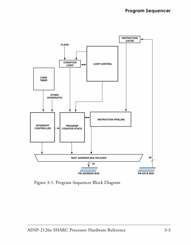
ADSP-2126x SHARC Processor Hardware Reference 3-3
Program Sequencer
Figure 3-1. Program Sequencer Block Diagram
CORETIMER
INTERRUPTCONTROLLER
PROGRAMCOUNTER STACK
NEXT ADDRESS MULTIPLEXER
INSTRUCTIONCACHE
INSTRUCTION PIPELINE
LOOP CONTROLCONDITION
LOGIC
FLAGS
PM ADDRESS BUS PM DATA BUS
48
24
OTHERINTERRUPTS
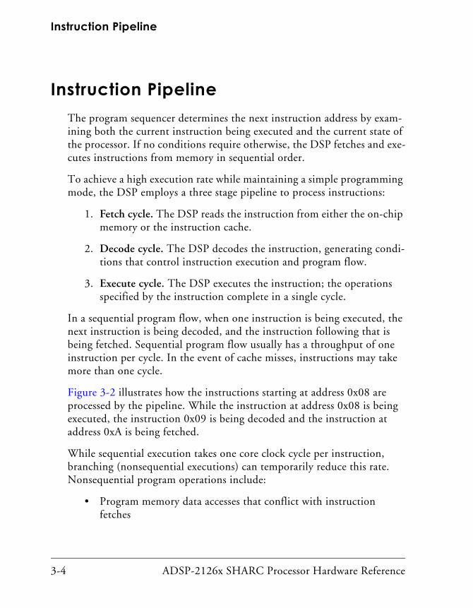
Instruction Pipeline
3-4 ADSP-2126x SHARC Processor Hardware Reference
Instruction PipelineThe program sequencer determines the next instruction address by exam-ining both the current instruction being executed and the current state of the processor. If no conditions require otherwise, the DSP fetches and exe-cutes instructions from memory in sequential order.
To achieve a high execution rate while maintaining a simple programming mode, the DSP employs a three stage pipeline to process instructions:
1. Fetch cycle. The DSP reads the instruction from either the on-chip memory or the instruction cache.
2. Decode cycle. The DSP decodes the instruction, generating condi-tions that control instruction execution and program flow.
3. Execute cycle. The DSP executes the instruction; the operations specified by the instruction complete in a single cycle.
In a sequential program flow, when one instruction is being executed, the next instruction is being decoded, and the instruction following that is being fetched. Sequential program flow usually has a throughput of one instruction per cycle. In the event of cache misses, instructions may take more than one cycle.
Figure 3-2 illustrates how the instructions starting at address 0x08 are processed by the pipeline. While the instruction at address 0x08 is being executed, the instruction 0x09 is being decoded and the instruction at address 0xA is being fetched.
While sequential execution takes one core clock cycle per instruction, branching (nonsequential executions) can temporarily reduce this rate. Nonsequential program operations include:
• Program memory data accesses that conflict with instruction fetches

ADSP-2126x SHARC Processor Hardware Reference 3-5
Program Sequencer
• Jumps
• Subroutine calls and returns
• Interrupts and returns
• Loops
Instruction CacheUsually, the sequencer fetches an instruction from memory on each cycle. Occasionally, bus constraints prevent some of the data and instructions from being fetched in a single cycle. To alleviate these data flow conflicts, the DSP has a large 32-location instruction cache that caches instructions that cause these conflicts. This solution removes the need to fetch the offending instruction from memory, which frees both memory blocks and data buses for data accesses. Except for enabling or disabling, the caches operation is completely automatic and transparent, requiring no user intervention. For more information, see “Using the Cache” on page 3-8.
Bus ConflictsA bus is comprised of two parts: the address bus and the data bus. Because the bus can be accessed continually by different sources (illustrated in Figure 3-1 on page 3-3), there is a potential for bus or block conflicts.
Figure 3-2. Pipelined Execution Cycles
CLOCK CYCLES
EXECUTEINSTRUCTION
DECODEINSTRUCTION
FETCHINSTRUCTION
1 2 3 4 5
0x08
0x08
0x08
0x09
0x09
0x09
0x0A
0x0A
0x0A
0x0B
0x0B
0x0C

Instruction Cache
3-6 ADSP-2126x SHARC Processor Hardware Reference
A bus conflict occurs when the PM data bus, normally used to fetch an instruction in each cycle, is used to fetch instruction and to access data. Because of the three stage instruction pipeline, as the DSP executes an instruction (at address n) it also uses the PM bus to access data. For sequential executions, this creates a conflict with the instruction fetch (at address n+2).
The cache stores the fetched instruction (n+2), not the instruction requiring the program memory data access.
Block conflicts differ from bus conflicts in that block conflicts occur when there are multiple outstanding writes to the same memory block or to the same word in a different block. When the DSP first encounters a bus con-flict, it must stall for one cycle while the data is transferred, and then fetch the instruction on the following cycle. To prevent the same delay from happening again, the DSP automatically writes the fetched instruction to the cache. The sequencer checks the instruction cache on every data access using the PM bus. If the instruction needed is in the cache, a “cache hit” occurs—the instruction fetch from the cache happens in parallel with the program memory data access, without incurring a delay.
If the instruction needed is not in the cache, a “cache miss” occurs, and the instruction fetch (from memory) takes place in the cycle following the program memory data access, incurring one cycle of overhead. This instruction is loaded into the cache (if the cache is enabled and not fro-zen), so that it is available the next time the same instruction (that requires program memory data) is executed.
Figure 3-3 shows a block diagram of the instruction cache. The cache holds 32 instuction-address pairs. These pairs (or cache entries) are arranged into 16 (15-0) cache sets according to the four least significant bits (3-0) of their address. The two entries in each set (entry 0 and entry 1) have a valid bit, indicating if the entry contains a valid instruction. The least recently used (LRU) bit for each set indicates which entry was not placed in the cache last (0=entry 0 and 1=entry 1).

ADSP-2126x SHARC Processor Hardware Reference 3-7
Program Sequencer
The cache places instructions in entries according to the four LSBs of the instruction’s address. When the sequencer checks for an instruction to fetch from the cache, it uses the four address LSBs as an index to a cache set. Within that set, the sequencer checks the addresses of the two entries as it looks for the needed instruction. If the cache contains the instruction, the sequencer uses the entry and updates the LRU bit (if necessary) to indi-cate the entry did not contain the needed instruction.
When the cache does not contain a needed instruction, it loads a new instruction and its address and places them in the least recently used entry of the appropriate cache set. The cache then toggles the LRU bit, if necessary.
Block ConflictsA bus conflict occurs when an instruction fetch and a data access are made on the same bus. Similarly, a block conflict occurs when multiple accesses
Figure 3-3. Instruction Cache Architecture
INSTRUCTIONS
SET0
SET1
SET2
SET13
SET14
SET15
ADDRESSESBITS (23-4)
LRUBIT
VALIDBIT
ENTRY 0
ENTRY 0
ENTRY 0
ENTRY 1
ENTRY 1
ENTRY 1
ENTRY 0
ENTRY 0
ENTRY 0
ENTRY 1
ENTRY 1
ENTRY 1
ADDRESSESBITS (3-0)
0000
0001
0010
1101
1110
1111

Instruction Cache
3-8 ADSP-2126x SHARC Processor Hardware Reference
are made to the same block in internal memory. This scenario occurs when data is accessed from the same block from which the instructions are executed. This scenario also occurs when an instruction performs both a DM and PM access to the same block in one instruction. In the first case, the instruction takes two cycles to complete, with the data being accessed in the first cycle and the instruction in the second. In the latter case, where a dual data access is performed, the processor takes three cycles to com-plete the instruction.
Block conflicts are not cached.
Using the CacheAfter a DSP reset, the cache is cleared (it contains no instructions), unfro-zen, and enabled. From then on, the MODE2 register controls the operating mode of the instruction cache as shown below.
• Cache Disable. Bit 4 (CADIS) directs the sequencer to disable the cache (if 1) or enable the cache (if 0).
• Cache Freeze. Bit 19 (CAFRZ) directs the sequencer to freeze the contents of the cache (if 1) or let new entries displace the entries in the cache (if 0).
Table A-3 on page A-8 lists all the bits in the MODE2 register.
Freezing the cache prevents any changes to its contents—a cache miss does not result in a new instruction being stored in the cache. Disabling the cache stops its operation completely; all instruction fetches conflicting with program memory data accesses are delayed by the access. These func-tions are selected by the CADIS (cache enable/disable) and CAFRZ (cache freeze) bits in the MODE2 register.
The cache content stays valid when the cache is disabled. The effect of dis-abling the cache is that an already cached instruction does not generate a

ADSP-2126x SHARC Processor Hardware Reference 3-9
Program Sequencer
cache hit. The same instruction does generate a hit and can be taken from the cache after the cache is enabled.
If the cache freeze bit of the MODE2 register is set by a program memory data access instruction n, then the n+2 instruction is cached. This results from the effect latency of the MODE2 register.
When a program changes the cache mode, an instruction contain-ing a program memory data access must not be placed directly after a cache enable or cache disable instruction. This is because the DSP must wait at least one cycle before executing the PM data access. A program should have a NOP or other non-conflicting instruction inserted after the cache enable instruction.
Optimizing Cache UsageCache operation is usually efficient and requires no intervention. How-ever, certain ordering of instructions can work against the cache’s architecture, reducing its efficiency. When the order of PM data accesses and instruction fetches continuously displaces cache entries and loads new entries, the cache does not operate efficiently. Rearranging the order of these instructions remedies this inefficiency. Optionally, a dummy PM read can be inserted to trigger the cache.
When a cache miss occurs, the needed instruction is loaded into the cache so that if the same instruction is needed again, it will be there (that is, a cache hit will occur). However, if another instruction whose address is mapped to the same set displaces this instruction, a cache miss occurs. The LRU bits help to reduce this possibility since at least two other instructions, mapped to the same set, are needed before an instruction is displaced. If three instructions mapped to the same set are all needed repeatedly, cache efficiency (that is, “hit rate”) can go to zero. To solve this problem, move one or more instructions to a new address that is mapped to a different cache set.

Instruction Cache
3-10 ADSP-2126x SHARC Processor Hardware Reference
An example of inefficient cache code appears in Table 3-1. The PM bus data access at address 0x101 in the loop, Outer, causes a bus conflict and also causes the cache to load the instruction being fetched at 0x103 (into set 3). Each time the program calls the subroutine, Inner, the program memory data accesses at 0x201 and 0x211 displace the instruction at 0x103 by loading the instructions at 0x203 and 0x213 (also into set 3). If the program rarely calls the Inner subroutine during the Outer loop exe-cution, the repeated cache loads do not greatly influence performance. If the program frequently calls the subroutine while in the loop, cache ineffi-ciency has a noticeable effect on performance. To improve cache efficiency on this code (if for instance, execution of the Outer loop is time critical), rearrange the order of some instructions. Moving the subroutine call up one location (starting at 0x201) also works. By using that order, the two cached instructions end up in cache set 4, instead of set 3.
Table 3-1. Cache Inefficient Code
Address Instruction
0x0100 lcntr = 1024, do Outer until LCE;
0x0101 r0 = dm(i0,m0), pm(i8,m8) = f3;
0x0102 r1 = r0 – r15;
0x0103 if eq call (Inner);
0x0104 f2 = float r1;
0x0105 f3 = f2 * f2;
0x0106 Outer: f3 = f3 + f4;
0x0107 pm(i8,m8) = f3;
...
0x0200 Inner: r1 = R13;
0x0201 r14 = pm(i9,m9);
...
0x0211 pm(i9,m9) = r12;

ADSP-2126x SHARC Processor Hardware Reference 3-11
Program Sequencer
Branches and SequencingOne type of nonsequential program flow that the sequencer supports is branching. A branch occurs when a JUMP or CALL/RETURN instruction moves execution to a location other than the next sequential address. For descriptions on how to use JUMP and CALL/RETURN instructions, see the SHARC Processor Programming Reference. Briefly, these instructions oper-ate as follows.
• A JUMP or a CALL instruction transfers program flow to another memory location. The difference between a JUMP and a CALL is that a CALL automatically pushes the return address (the next sequential address after the CALL instruction) onto the PC stack. This push makes the address available for the CALL instruction’s matching return from an RTS subroutine instruction.
• A RETURN instruction causes the sequencer to fetch the instruction at the return address, which is stored at the top of the PC stack. The two types of return instructions are return from subroutine (RTS) and return from interrupt (RTI). While the RTS only pops the return address off the PC stack, the RTI pops the return address and:
1. Clears the interrupt’s bit in the interrupt latch register (IRPTL) and allows another interrupt to be latched in the IRPTL register and the interrupt mask pointer (IMASKP) register. See Table A-9 on page A-27.
...
0x021F rts;
Table 3-1. Cache Inefficient Code (Cont’d)
Address Instruction

Branches and Sequencing
3-12 ADSP-2126x SHARC Processor Hardware Reference
2. Pops the status stack if the ASTATx/y and MODE1 status registers that have been pushed for interrupts IRQ2-0 or timers.
There are a number of parameters that can be specified for branching instructions:
• Branches can be direct or indirect. For direct branches, the sequencer generates the address; for indirect branches, the PM data address generator (DAG2) produces the address
• Direct branches are JUMP or CALL/RETURN instructions that use an absolute—not changing at run time—address (such as a program label) or use a PC-relative address. Some instruction examples that cause a direct branch are:
CALL fft1024; /* Where fft1024 is an address label */
JUMP (pc,10); /* Where (pc,10) is a PC-relative address */
Indirect branches are JUMP or CALL/RETURN instructions that use a dynamic address that comes from the PM data address generator (DAG2). For more information on the data address generator, see “Data Address Generators” on page 4-1. Some instruction exam-ples that cause an indirect branch are:
JUMP (i12, m8); /* where (m8,i12) are DAG2 registers */
CALL (i13, m9); /* where (m9,i13) are DAG2 registers */
Conditional BranchesThe sequencer supports conditional branches. These conditional branches are JUMP or CALL/RETURN instructions whose execution is based on testing an IF condition. For more information on condition types in IF condition instructions, see “Conditional Sequencing” on page 3-18. Note that the DSP’s Single-Instruction, Multiple-Data (SIMD) mode influences the execution of conditional branches. For more information, see “Summary” on page 3-61.

ADSP-2126x SHARC Processor Hardware Reference 3-13
Program Sequencer
Delayed BranchesThe instruction pipeline influences how the sequencer handles delayed branches. For immediate branches in which JUMP and CALL/RETURN instructions are not specified as delayed branches (DB), two instruction cycles are lost (NOP) as the pipeline empties and refills with instructions from the new branch.
As shown in Table 3-2 and Table 3-2, the DSP aborts the two instructions after the branch, which are in the fetch and decode stages. For a CALL, the decode address (the address of the instruction after the CALL) is the return address. During the two lost NOP cycles, the pipeline fetches and decodes the first instruction at the branch address.
In the illustrations that follow, shading indicates aborted instructions, which are followed by NOP instructions.
Table 3-2. Pipelined Execution Cycles for Immediate Branch(Jump/Call)
Cycles 1 2 3 4
Execute N NOP NOP J2
Decode N + 1–>NOP1 N + 2–>NOP3 J2 J + 1
Fetch N + 2 J2 J + 1 J + 2
1. N + 1 suppressed2. For call, N + 1 pushed onto PC stack3. N + 2 suppressed
Table 3-3. Pipelined Execution Cycles for Immediate Branch (Return)
Cycles 1 2 3 4
Execute N NOP NOP R
Decode N + 1–>NOP1 N + 2–>NOP3 R R + 1
Fetch N + 2 R2 R + 1 R + 2
1. N + 1 suppressed2. R (N + 1 in Figure 2-14 on page...)popped from PC stack3. N + 2 suppressed

Branches and Sequencing
3-14 ADSP-2126x SHARC Processor Hardware Reference
In delayed branch, JUMP and CALL/RETURN instructions that use the delayed branches (DB) modifier, no instruction cycles are lost in the pipeline. This is because the DSP executes the two instructions after the branch while the pipeline fills with instructions from the new location. This is shown in the sample code below.
call fft1024 (DB);
...
...
jump (pc,10) (DB);
As shown in Table 3-4 and Table 3-5, the DSP executes the two instruc-tions after the branch, while the instruction at the branch address is fetched and decoded. In the case of a CALL, the return address is the third address after the branch instruction. While delayed branches use the instruction pipeline more efficiently than immediate branches, delayed branch code can be harder to understand because of the instructions between the branch instruction and the actual branch.
Table 3-4. Pipelined Execution Cycles for Delayed Branch (JUMP or CALL)
Cycles 1 2 3 4
Execute N N + 1 N + 2 J
Decode N + 1 N + 2 J J + 1
Fetch N + 2 J1 J + 1 J + 2
N is the branching instruction, and J is the instruction branch address.1. For a delayed branch call, N + 3 is pushed on PC stack, not N + 1
Table 3-5. Pipelined Execution Cycles for Delayed Branch (Return)
Cycles 1 2 3 4
Execute N1 N + 1 N + 2 R
Decode N + 1 N + 2 R R + 1
Fetch N + 2 R R + 1 R + 2
N is the branching instruction, and R is the instruction at the return address.1. R (N + 3 pushed in figure...) popped from PC stack

ADSP-2126x SHARC Processor Hardware Reference 3-15
Program Sequencer
Besides being more challenging to code, delayed branches impose some limitations that stem from the instruction pipeline architecture. Because the delayed branch instruction and the two instructions that follow it must execute sequentially, the instructions in the two locations that follow a delayed branch instruction cannot be:
• Other branches (no JUMP, CALL, or RETURN instructions)
Normally, it is not valid to have two conditional instructions that use the (DB) option follow each other. However, where the execu-tion of those instructions is mutually exclusive, it is allowed. For example:
if gt jump (PC, 7) (db)
if le jump (PC,11) (db)
• Any stack manipulations (no PUSH or POP instructions or writes to the PC stack or PC stack pointer register)
• Any loops or other breaks in sequential operation (no DO/UNTIL or IDLE instructions)
Development software for the DSP should always flag these types of instructions as code errors in the two locations after a delayed branch instruction.
Delayed branches and the instruction pipeline also influence interrupt processing. Because the delayed branch instruction and the two instruc-tions that follow it always execute sequentially, the DSP does not immediately process an interrupt that occurs in between a delayed branch instruction and either of the two instructions that follow. Any interrupt that occurs during these instructions is latched, but is not processed until the branch is complete.
This may be useful when two instructions must execute atomically (with-out interruption), such as when working with semaphores. In the

Loop and Status Stacks and Sequencing
3-16 ADSP-2126x SHARC Processor Hardware Reference
following example, instruction 2 immediately follows instruction 1 in all occasions:
jump (pc, 3) (db):
instruction 1;instruction 2;
During a delayed branch, a program can read the PC stack register or PC stack pointer register. This read shows that the return address on the PC stack has already been pushed or popped, even though the branch has not yet occurred.
Loop and Status Stacks and SequencingThe sequencer includes a Program Counter (PC) stack, which appears in Figure 3-1 on page 3-3. At the start of a subroutine or loop, the sequencer pushes return addresses for subroutines (CALL/RETURN instructions) and top-of-loop addresses for loops (DO/UNTIL instructions) onto the PC stack. The sequencer pops the PC stack during a return from interrupt (RTI), return from subroutine (RTS), and a loop termination.
The Program Counter (PC) register is the last stage in the fetch-decode-execute instruction pipeline. It contains the 24-bit address of the instruction the DSP will execute on the next cycle. The PC register, combined with the Program Counter Stack (PCSTK) register, stores return addresses and top-of-loop addresses.
The PC stack is 30 locations deep. The stack is full when all entries are occupied, is empty when no entries are occupied, and is overflowed if a

ADSP-2126x SHARC Processor Hardware Reference 3-17
Program Sequencer
push occurs when the stack is full. The following bits in the STKYx register indicate the PC stack full and empty states.
• PC stack full. Bit 21 (PCFL) indicates that the PC stack is full (if 1) or not full (if 0)—not a sticky bit, cleared by a POP.
• PC stack empty. Bit 22 (PCEM) indicates that the PC stack is empty (if 1) or not empty (if 0)—not sticky, cleared by a PUSH.
Table A-5 on page A-17 lists all the bits in the STYKx register.
To prevent a PC stack overflow, the PC stack full condition generates the (maskable) stack overflow interrupt (SOVFI). This interrupt occurs when the PC stack has 29 of 30 locations filled (the almost full state). The PC stack full interrupt occurs when at this point because the PC stack full interrupt service routine needs that last location for its return address.
The address of the top of the PC stack is available in the PC stack pointer (PCSTKP) register. The value of PCSTKP is zero when the PC stack is empty, is 1 through 30 when the stack contains data, and is 31 when the stack overflows. A write to PCSTKP takes effect after a one cycle delay. If the PC stack is overflowed, a write to PCSTKP has no effect. This register can be read from and written to.
The overflow and full flags provide diagnostic aid only. Programs should not use these flags for runtime recovery from overflow. Note that the sta-tus stack, loop stack overflow, and PC stack full conditions trigger a maskable interrupt.
The empty flags can ease stack saves to memory. Programs can monitor the empty flag when saving a stack to memory to determine when the DSP has transferred all values.

Conditional Sequencing
3-18 ADSP-2126x SHARC Processor Hardware Reference
Conditional SequencingThe sequencer supports conditional execution with conditional logic, as illustrated in Figure 3-6 on page 3-62. This logic evaluates conditions for conditional (IF) instructions and loop (DO/UNTIL) terminations. The con-ditions are based on information from the arithmetic status registers (ASTATx and ASTATy), the mode control 1 register (MODE1), the flag inputs, and the loop counter. For more information on arithmetic status, see “Using Computational Status” on page 2-15. When in SIMD mode, con-ditional execution is effected by the arithmetic status of both processing elements. For information on conditional sequencing in SIMD mode, see “Summary” on page 3-61.
Each condition that the DSP evaluates has an assembler mnemonic. The condition mnemonics for conditional instructions appear in Table 3-6. For most conditions, the sequencer can test both true and false states. For example, the sequencer can evaluate ALU equal-to-zero (EQ) and ALU not-equal-to-zero (NZ).
To branch conditionally based on the value of a register, a program can use the Test Flag (TF) condition generated from a Bit Test Flag (BTF) instruction. The TF flag is set or cleared as a result of a BIT TST or BIT XOR instruction, which can test the contents of any of the DSP’s system regis-ters, including STKYx and STKYy.

ADSP-2126x SHARC Processor Hardware Reference 3-19
Program Sequencer
Table 3-6. IF Condition and DO/UNTIL Termination Mnemonics
Condition From Description True if… Mnemonic
ALU ALU = 0 AZ = 1 EQ
ALU ≠ 0 AZ = 0 NE
ALU > 0 footnote1 GT
ALU < zero footnote2 LT
ALU ≥ 0 footnote3 GE
ALU ≤ 0 footnote4 LE
ALU carry AC = 1 AC
ALU not carry AC = 0 NOT AC
ALU overflow AV = 1 AV
ALU not overflow AV = 0 NOT AV
Multiplier Multiplier overflow MV = 1 MV
Multiplier not overflow MV= 0 NOT MV
Multiplier sign MN = 1 MS
Multiplier not sign MN = 0 NOT MS
Shifter Shifter overflow SV = 1 SV
Shifter not overflow SV = 0 NOT SV
Shifter zero SZ = 1 SZ
Shifter not zero SZ = 0 NOT SZ
System register manipulation logic
Bit test flag true BTF = 1 TF
Bit test flag false BTF = 0 NOT TF

Conditional Sequencing
3-20 ADSP-2126x SHARC Processor Hardware Reference
The two conditions that do not have complements are LCE/NOT LCE (loop counter expired/not expired) and TRUE/FOREVER. The context of these con-dition codes determines their interpretation. Programs should use TRUE and NOT LCE in conditional (IF) instructions. Programs should use FOR-EVER and LCE to specify loop (DO/UNTIL) termination. A DO FOREVER instruction executes a loop indefinitely, until an interrupt or reset intervenes.
Flag Input Flag0 asserted FI0 = 1 FLAG0_IN
Flag0 not asserted FI0 = 0 NOT FLAG0_IN
Flag1 asserted FI1 = 1 FLAG1_IN
Flag1 not asserted FI1 = 0 NOT FLAG1_IN
Flag2 asserted FI2 = 1 FLAG2_IN
Flag2 not asserted FI2 = 0 NOT FLAG2_IN
Flag3 asserted FI3 = 1 FLAG3_IN
Flag3 not asserted FI3 = 0 NOT FLAG3_IN
Hardware Loop Loop counter expired (Do) CURLCNTR = 1 LCE
Loop counter not expired (IF) CURLCNTR ≠ 1 NOT ICE
Always false (Do) Always FOREVER
Always true (IF) Always TRUE
1 ALU greater than (GT) is true if: [AF and (AN xor (AV and ALUSAT)) or (AF and AN)] or AZ = 0
2 ALU less than (LT) is true if: [AF and (AN xor (AV and ALUSAT)) or (AF and AN and AZ)] = 1
3 ALU greater equal (GE) is true if: [AF and (AN xor (AV and ALUSAT)) or (AF and AN and AZ)] = 0
4 ALU lesser or equal (LT) is true if: [AF and (AN xor (AV and ALUSAT)) or (AF and AN)] or AZ = 1
Table 3-6. IF Condition and DO/UNTIL Termination Mnemonics (Cont’d)
Condition From Description True if… Mnemonic

ADSP-2126x SHARC Processor Hardware Reference 3-21
Program Sequencer
There are some restrictions on how programs may use conditions in DO/UNTIL loops. For more information, see “Restrictions on Ending Loops” on page 3-27 and “Restrictions on Short Loops” on page 3-28.
Core StallsLike all previous SHARC processors, there are a number of conditions that cause the core to temporarily stop fetching and executing further instructions. This event, known as a core stall, occurs when an instruction accesses a peripheral’s data-buffer. Specifically, the core stalls when it reads an empty receive buffer or writes a full transmit buffer. Execution resumes once the peripheral moves a valid word of data into the receive buffer or when the peripheral sends one word out from the transmit buffer.
In addition to standard core stall situations, there are four other condi-tions that cause the ADSP-2126x core to stall. The following instructions or sequences of instructions will cause the processor core to stall for one or more cycles. These stalls were introduced to facilitate the doubling of the core clock rate without modifying the 3-deep instruction-pipeline.
1. Reading or writing any memory mapped register in a conditional instruction stalls the core for one cycle. This means that a total of two cycles are needed for that instruction to complete.
2. Reading the System/Emulator memory-mapped registers shown in Table 3-7 stalls the processor for one cycle. Therefore, a total of two cycles are needed for that instruction.
Table 3-7. System/Emulator Memory-Mapped Registers
Register Address Register Address
EEMUIN 0x30020 PSA4S 0x300A6
EEMUSTAT 0x30021 PSA4E 0x300A7

Core Stalls
3-22 ADSP-2126x SHARC Processor Hardware Reference
3. Reading from all other memory-mapped registers and data-buffers (for example RXSPI, PPCTL, or SPISTAT) stalls the processor core for three cycles. Therefore, a total of four cycles is needed for that instruction to complete.
4. If the following sequence of three instructions is executed without any other instruction between them, then the processor stalls for one cycle.
a. Instruction 1: Compute instruction affecting flags such as R2 = R3 – R4;
b. Instruction 2: Conditional instruction involving post-mod-ify addressing such as IF EQ DM(I1,M1) = R15;
c. Instruction 3: Instruction involving post-modify or pre-modify addressing involving the same I register such as R0 = DM(I1,M2);
EEMUOUT 0x30022 DMA1S 0x300B2
SYSCTL 0x30024 DMA1E 0x300B3
BRKCTL 0x30025 DMA2S 0x300B4
REVPID 0x30026 DMA2E 0x300B5
PSA1S 0x300A0 PMDAS 0x300B8
PSA1E 0x300A1 PMDAE 0x300B9
PSA2S 0x300A2 EMUN 0x300AE
PSA2E 0x300A3 IOAS 0x300B0
PSA3S 0x300A4 IOAE 0x300B1
PSA3E 0x300A5
Table 3-7. System/Emulator Memory-Mapped Registers (Cont’d)
Register Address Register Address

ADSP-2126x SHARC Processor Hardware Reference 3-23
Program Sequencer
The stall occurs during the decode phase of Instruction 3. Instruc-tion 3 takes two cycles to complete decode.
Execution StallsThe following events can cause an execution stall for the ADSP-2126x:
• One cycle on a Program Memory Data Access with instruction cache miss
• Two cycles on non-delayed branches
• Two cycles on normal interrupts
• One to two cycles on short loops with small iterations
• n cycles on an IDLE instruction
• In a sequence of three instructions of the types shown below, the processor may stall for one cycle:
Instruction 1: Compute instruction affecting flags such as R2 = R3 - R4;
Instruction 2: Conditional instruction involving post-modify addressing such as IF EQ DM(I1,M1) = R15;
Instruction 3: Instruction such as R0 = DM(I1,M2); involving post-modify addressing involving same I register. This last instruc-tion stalls the processor for one cycle.
• Any read reference to a memory-mapped register located physically within core (registers like SYSCTL, which are not situated in the IOP) requires two cycles; therefore, the processor stalls for one cycle.

Core Stalls
3-24 ADSP-2126x SHARC Processor Hardware Reference
• Any read reference to a memory-mapped register located within a peripheral such as the SPI, SPORTS, IDP, or parallel port requires a minimum of four cycles; so the minimum stall is three cycles.
• Any reference to a memory-mapped register in a conditional instruction stalls the processor for one extra cycle (with respect to an unconditional instruction).
DAG StallsOne cycle hold on register conflict.
Memory StallsOne cycle on PM and DM bus access to the same block of internal memory.
IOP Register StallsRead of the IOP registers takes a minimum of four cycles, therefore the processor stalls for at least three cycles.
DMA StallsThe following events can cause a DMA stall for the ADSP-2126x:
• One cycle stall if an access to a DMA Parameter register conflicts with the DMA address generation. For example, writing to or read-ing from a DMA Parameter register while a register update is taking place conflicts with DMA chaining.
• n cycles if writing (or reading) to a DMA buffer when the buffer is full (or empty).

ADSP-2126x SHARC Processor Hardware Reference 3-25
Program Sequencer
• TCB loading takes 16 core clock cycles to configure 4 IOP regis-ters. This access is not divisible.
Loops and SequencingAnother type of nonsequential program flow that the sequencer supports is looping. A loop occurs when a DO/UNTIL instruction causes the DSP to repeat a sequence of instructions until a condition tests true. Unlike other processors, the SHARC automatically evaluates the loop termination con-dition and modifies the Program Counter (PC) register appropriately. This allows zero overhead looping.
In addition to the standard status flags available to all conditional instruc-tions (EQ, GT, LT, and so on), a special condition instruction Loop Counter Expired (LCE), is specifically used for terminating loops. This instruction tests whether the loop has completed the required number of iterations in the LCNTR register. Loops that terminate with conditions other than LCE have some additional restrictions. For more information, see “Restrictions on Ending Loops” on page 3-27 and “Restrictions on Short Loops” on page 3-28. For more information on condition types in DO/UNTIL instruc-tions, see “Interrupts and Sequencing” on page 3-48.
The DSP’s SIMD mode influences the execution of loops.
The DO/UNTIL instruction uses the sequencer’s loop and condition features, as shown in Figure 3-1 on page 3-3. These features provide efficient hard-ware loops without the overhead of additional instructions to branch, test a condition, or decrement a counter. The following code example shows a DO/UNTIL loop that contains three instructions and iterates 30 times.
LCNTR = 30, DO the_end UNTIL LCE; /*Loop iterates 30 times*/
R0 = DM(I0,M0), F2 = PM(I8,M8);
R1 = R0-R15;
the_end: F4 = F2 + F3; /*Last instruction in loop*/

Loops and Sequencing
3-26 ADSP-2126x SHARC Processor Hardware Reference
When executing a DO/UNTIL instruction, the program sequencer pushes the address of the loop’s last instruction and its termination condition onto the loop address stack. The sequencer also pushes the top-of-loop address—the address of the instruction following the DO/UNTIL instruc-tion—onto the PC stack.
The sequencer’s instruction pipeline architecture influences loop termina-tion. Because instructions are pipelined, the sequencer must test the termination condition and, if the loop is counter-based, decrement the counter before the end of the loop. Based on the test’s outcome, the next fetch either exits the loop or returns to the top-of-loop.
The termination condition test occurs when the DSP is executing the instruction that is two locations before the last instruction in the loop (at location e – 2, where e is the end-of-loop address). If the condition tests false, the sequencer repeats the loop and fetches the instruction from the top-of-loop address, which is stored on the top of the PC stack. If the con-dition tests true, the sequencer terminates the loop and fetches the next instruction after the end of the loop, popping the loop and PC stacks.
A special case of loop termination is the loop abort instruction, JUMP (LA). This instruction causes an automatic loop abort when it occurs inside a loop. When the loop aborts, the sequencer pops the PC and loop address stacks once. If the aborted loop was nested, the single pop of the stacks leaves the correct values in place for the outer loop.
Table 3-8 and Table 3-9 show the pipeline states for loop iteration and termination.

ADSP-2126x SHARC Processor Hardware Reference 3-27
Program Sequencer
Restrictions on Ending LoopsThe sequencer’s loop features (which optimize performance in many ways) limit the types of instructions that may appear at or near the end of the loop. These restrictions include:
• Nested loops cannot use the same end-of-loop instruction address.
• Nested loops with a non-counter-based loop as the outer loop must place the end address of the outer loop at least two addresses after the end address of the inner loop.
• Nested loops with a non-counter-based loop as the outer loop that use the loop abort instruction, JUMP (LA), to abort the inner loop, may not JUMP (LA) to the last instruction of the outer loop.
Table 3-8. Pipelined Execution Cycles for Loop Back (Iteration)
Cycles 1 2 3 4
Execute E – 21 E – 1 E B
Decode E – 1 E B B + 1
Fetch E B2 B + 1 B + 2
E is the loop end instruction, and B is the loop start instruction.1. Termination condition tests false2. Loop start address is the top of the PC stack
Table 3-9. Pipelined Execution Cycles for Loop Termination
Cycles 1 2 3 4
Execute E – 21 E – 1 E E + 1
Decode E – 1 E E + 1 E + 2
Fetch E E + 12 E + 2 E + 3
E is the loop end instruction.1. Termination condition tests true2. Loop aborts and loop stacks pop

Loops and Sequencing
3-28 ADSP-2126x SHARC Processor Hardware Reference
• An instruction that writes to the loop counter from memory can-not be used as the third-to-last instruction of a counter-based loop (at e–2, where e is the end-of-loop address).
• An IF NOT LCE instruction cannot be used as the instruction that follows a write to CURLCNTR from memory.
• Branch (JUMP or CALL/RETURN) instructions may not be used as any of the last three instructions of a loop. This no end-of-loop branches rule also applies to single instruction and two instruction loops with only one iteration.
There is one exception to the no end-of-loop branches rule. The last three instructions of a loop may contain an immediate CALL, a CALL without a DB modifier, that is paired with a loop re-entry return, a return (RTS) with loop reentry (LR) modifier. The immediate CALL may be one of the last three instructions of a loop, but not in a one instruction loop or a two instruction, single iteration loop.
Restrictions on Short LoopsThe sequencer’s pipeline features (which optimize performance in many ways) restrict how short loops iterate and terminate. Short loops (one or two instruction loops) terminate in a special way because they are shorter than the instruction pipeline. Counter-based loops (DO/UNTIL LCE) of one or two instructions are not long enough for the sequencer to check the ter-mination condition two instructions from the end of the loop. In these short loops, the sequencer has already looped back when the termination condition is tested. The sequencer provides special handling to prevent overhead (NOP) cycles if the loop is iterated a minimum number of times.
Table 3-10 and Table 3-11 show the pipeline execution for counter-based single instruction loops. Table 3-12 and Table 3-13 show the pipeline execution for counter-based two instruction loops. For no overhead, a loop of length one must be executed at least three times and a loop of length two must be executed at least twice. Loops of length one that

ADSP-2126x SHARC Processor Hardware Reference 3-29
Program Sequencer
iterate only once or twice and loops of length two that iterate only once incur two cycles of overhead, because two aborted instructions after the last iteration are needed to clear the instruction pipeline.
Table 3-10. Pipelined Execution Cycles for Single Instruction Counter-based Loop with Three Iterations
Cycles 1 2 3 4 5
Execute N1 N + 1 (Pass 1) N + 1 (Pass 2) N + 1 (Pass 3) N + 2
Decode N + 1 N + 1 N + 1 N + 2 N + 3
Fetch N + 2 N + 12 N + 23 N + 3 N + 4
N is the loop start instruction and N + 2 is the instruction after the loop.1. Loop count (LCNTR) equals 32. No opcode latch or fetch address update; count expired tests true3. Loop iteration aborts; PC and loop stacks pop
Table 3-11. Pipelined Execution Cycles for Single Instruction Counter-based Loop with Two Iterations (Two Overhead Cycles)
Cycles 1 2 3 4 5 6
Execute N1 N + 1 (Pass 1) N + 1 (Pass 2) NOP NOP N + 2
Decode N + 1 N + 1 N + 1 –>
NOP4N + 1 –>
NOP5N + 2 N + 3
Fetch N + 2 N + 12 N + 13 N + 2 N + 3 N + 4
N is the loop start instruction and N + 3 is the instruction after the loop.1. Loop count (LCNTR) equals 22. PC Stack supplies loop start address3. Count expired tests true4. Loop iteration aborts; PC and loop stacks pop
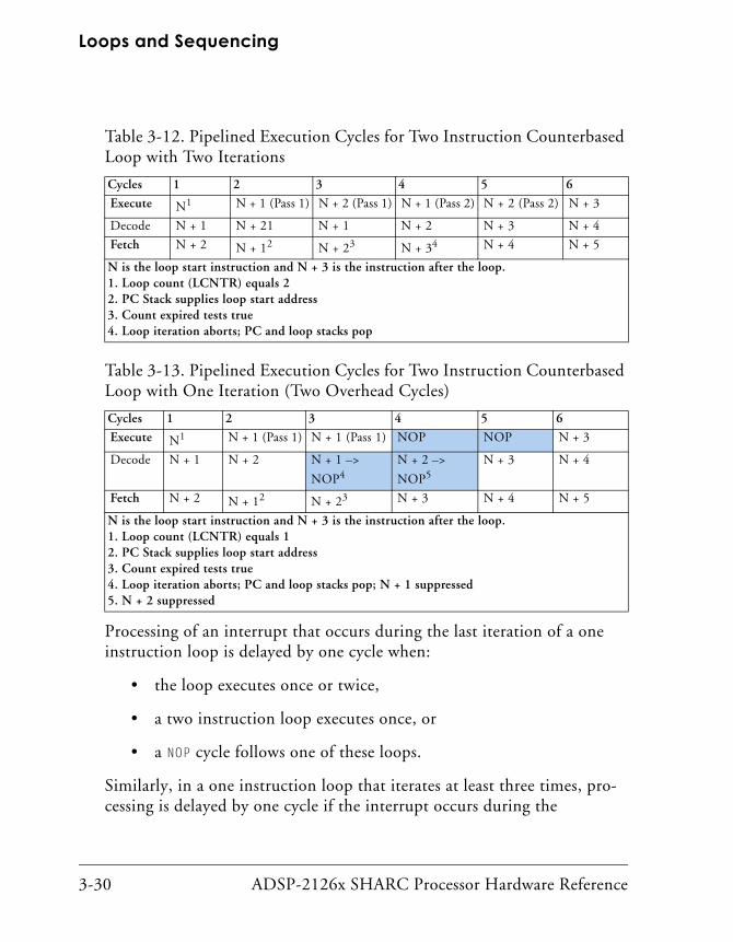
Loops and Sequencing
3-30 ADSP-2126x SHARC Processor Hardware Reference
Processing of an interrupt that occurs during the last iteration of a one instruction loop is delayed by one cycle when:
• the loop executes once or twice,
• a two instruction loop executes once, or
• a NOP cycle follows one of these loops.
Similarly, in a one instruction loop that iterates at least three times, pro-cessing is delayed by one cycle if the interrupt occurs during the
Table 3-12. Pipelined Execution Cycles for Two Instruction Counterbased Loop with Two Iterations
Cycles 1 2 3 4 5 6
Execute N1 N + 1 (Pass 1) N + 2 (Pass 1) N + 1 (Pass 2) N + 2 (Pass 2) N + 3
Decode N + 1 N + 21 N + 1 N + 2 N + 3 N + 4
Fetch N + 2 N + 12 N + 23 N + 34 N + 4 N + 5
N is the loop start instruction and N + 3 is the instruction after the loop.1. Loop count (LCNTR) equals 22. PC Stack supplies loop start address3. Count expired tests true4. Loop iteration aborts; PC and loop stacks pop
Table 3-13. Pipelined Execution Cycles for Two Instruction Counterbased Loop with One Iteration (Two Overhead Cycles)
Cycles 1 2 3 4 5 6
Execute N1 N + 1 (Pass 1) N + 1 (Pass 1) NOP NOP N + 3
Decode N + 1 N + 2 N + 1 –>
NOP4N + 2 –>
NOP5N + 3 N + 4
Fetch N + 2 N + 12 N + 23 N + 3 N + 4 N + 5
N is the loop start instruction and N + 3 is the instruction after the loop.1. Loop count (LCNTR) equals 12. PC Stack supplies loop start address3. Count expired tests true4. Loop iteration aborts; PC and loop stacks pop; N + 1 suppressed5. N + 2 suppressed

ADSP-2126x SHARC Processor Hardware Reference 3-31
Program Sequencer
third-to-last iteration. For more information on pipeline execution during interrupts, see “Interrupts and Sequencing” on page 3-48.
Short noncounter-based loops terminate differently from short coun-ter-based loops. These differences stem from the architecture of the pipeline and conditional logic:
• In a three instruction non counter-based loop, the sequencer tests the termination condition when the DSP executes the top of loop instruction. When the condition tests true, the sequencer com-pletes the iteration of the loop and terminates.
• In a two instruction non counter-based loop, the sequencer tests the termination condition when the DSP executes the last (second) instruction. If the condition becomes true when the first instruc-tion is executed, and the condition tests true during the second instruction, then the sequencer completes one more iteration of the loop before exiting. If the condition becomes true during the sec-ond instruction, the sequencer completes two more iterations of the loop before exiting.
• In a one instruction non counter-based loop, the sequencer tests the termination condition every cycle. After the cycle when the condition becomes true, the sequencer completes three more itera-tions of the loop before exiting. But if the one instruction used in the loop is a PM instruction, then the loop is executed only two more times.
Loop Address StackThe sequencer’s loop support, shown in Figure 3-1 on page 3-3, includes a loop address stack. The loop address stack is six levels deep by 32 bits wide.
The LADDR register contains the top entry on the loop address stack. This register is readable and writable over the DM data bus. Reading from and

Loops and Sequencing
3-32 ADSP-2126x SHARC Processor Hardware Reference
writing to LADDR does not move the loop address stack pointer; only a stack push or pop performed with explicit instructions moves the stack pointer. LADDR contains the value 0xFFFF FFFF when the loop address stack is empty. “Loop Address Stack Register (LADDR)” on page A-34 lists all the bits in the LADDR register.
The sequencer pushes an entry onto the loop address stack when executing a DO/UNTIL or PUSH loop instruction. The stack entry pops off the stack two instructions before the end of its loop’s last iteration or on a POP loop instruction. A stack overflow occurs if a seventh entry (one more than full) is pushed onto the loop stack. The stack is empty when no entries are occupied.
The loop stacks’ overflow or empty status is available. Because the sequencer keeps the loop stack and loop counter stack synchronized, the same overflow and empty flags apply to both stacks. These flags are in the sticky status register (STKYx). For more information on STKYx, see Table A-5 on page A-17. For more information on how these flags work with the loop stacks, see “Loop Counter Stack” on page 3-32. Note that a loop stack overflow causes a maskable interrupt.
Because the sequencer tests the termination condition two instructions before the end of the loop, the loop stack pops before the end of the loop’s final iteration. If a program reads LADDR at either of these instructions, the value is already the termination address for the next loop stack entry.
Loop Counter StackThe sequencer’s loop support, shown in Figure 3-1 on page 3-3, includes a loop counter stack. The sequencer keeps the loop counter stack synchro-nized with the loop address stack. Both stacks always have the same number of locations occupied. Because these stacks are synchronized, the same empty and overflow status flags from the STKYx register apply to both stacks.

ADSP-2126x SHARC Processor Hardware Reference 3-33
Program Sequencer
The loop counter stack is six locations deep. The stack is full when all entries are occupied, is empty when no entries are occupied, and is over-flowed if a push occurs when the stack is already full. The following bits in the STKYx register indicate the loop counter stack full and empty states.
• Loop stacks overflowed. Bit 25 (LSOV) indicates that the loop counter stack and loop stack are overflowed (if set to 1) or not overflowed (if set to 0)— LSOV is a sticky bit.
• Loop stacks empty. Bit 26 (LSEM) indicates that the loop counter stack and loop stack are empty (if set to 1) or not empty (if set to 0)—not sticky, cleared by a PUSH.
Within the sequencer, the current loop counter (CURLCNTR) and loop counter (LCNTR) registers allow access to the loop counter stack. The CURL-CNTR register tracks iterations for a loop being executed, and the LCNTR register holds the count value before the loop is executed. The two coun-ters let the DSP maintain the count for an outer loop, while a program is setting up the count for an inner loop.
The top entry in the loop counter stack (CURLCNTR) always contains the current loop count. This register is readable and writable over the DM data bus. Reading CURLCNTR when the loop counter stack is empty returns the value 0xFFFF FFFF.
The sequencer decrements the value of CURLCNTR for each loop iteration. Because the sequencer tests the termination condition two instruction cycles before the end of the loop, the loop counter also decrements before the end of the loop. If a program reads CURLCNTR at either of the last two loop instructions, the value is already the count for the next iteration.
The loop counter stack pops two instructions before the end of the last loop iteration. When the loop counter stack pops, the new top entry of the stack becomes the CURLCNTR value—the count in effect for the executing loop. If there is no executing loop, the value of CURLCNTR is 0xFFFF FFFF after the pop.

Loops and Sequencing
3-34 ADSP-2126x SHARC Processor Hardware Reference
Writing CURLCNTR does not cause a stack push. If a program writes a new value to CURLCNTR, the program changes the count value of the loop cur-rently executing. When a DO/UNTIL LCE loop is not executing, writing to CURLCNTR has no effect. Because the processor must use CURLCNTR to per-form counter-based loops, some restrictions relating to how a program can write CURLCNTR apply. See “Restrictions on Ending Loops” on page 3-27 for more information.
The next-to-top entry in the loop counter stack (LCNTR) is the location on the stack that takes effect on the next loop stack push. To set up a count value for a nested loop without changing the count for the currently exe-cuting loop, a program writes the count value to LCNTR.
A value of zero in LCNTR causes a loop to execute 232 times.
A DO/UNTIL LCE instruction pushes the value of LCNTR onto the loop count stack, making that value the new CURLCNTR value. Figure 3-4 demonstrates this process for a set of nested loops. The previous CURLCNTR value is pre-served one location down in the stack. If a program reads the LCNTR when the loop counter stack is full, the stack returns invalid data. When the loop counter stack is full, the stack discards any data written to LCNTR.

ADSP-2126x SHARC Processor Hardware Reference 3-35
Program Sequencer
Figure 3-4. Pushing the Loop Counter Stack for Nested Loops
1
AAAA AAAALCNTR
CURLCNTR
LCNTR
4
AAAA AAAA
DDDD DDDD
CCCC CCCC
BBBB BBBB
AAAA AAAA
0XFFFF FFFF
LCNTR
CURLCNTR
CURLCNTR
LCNTR
3
AAAA AAAA
CCCC CCCC
BBBB BBBB
CURLCNTR
LCNTR
6
BBBB BBBB
AAAA AAAA
DDDD DDDD
CCCC CCCC
FFFF FFFF
EEEE EEEE
CURLCNTR
7
BBBB BBBB
DDDD DDDD
FFFF FFFF
CCCC CCCC
EEEE EEEE
AAAA AAAA
CURLCNTR
LCNTR
2
AAAA AAAA
BBBB BBBB
CURLCNTR
LCNTR
5
AAAA AAAA
BBBB BBBB
CCCC CCCC
DDDD DDDD
EEEE EEEE
SIMD Mode and Sequencing
3-36 ADSP-2126x SHARC Processor Hardware Reference
Reading From LCNTR in a LOOP
If a program reads LCNTR during the last two instructions of a terminating loop, the value of LCNTR is the last CURLCNTR value for the loop. For example:
R12=0x8;LCNTR = R12, do (PC,7) until lce;nop;nop;nop;nop;nop;dm(I0,M0) = LCNTR;dm(I0,M0) = LCNTR;---------------------------------------LCNTR is 8 in first 7 iterations, in the last iteration it is 1.
SIMD Mode and SequencingThe DSP supports a SIMD (Single-Instruction, Multiple-Data) mode. In this mode, both of the DSP’s processing elements (PEx and PEy) execute instructions and generate status conditions. For more information on SIMD computations, see “SIMD (Computational) Operations” on page 2-49.
Because the two processing elements can generate different outcomes, the sequencers must evaluate conditions from both elements (in SIMD mode) for conditional (IF) instructions and loop (DO/UNTIL) terminations. The DSP records status for the PEx element in the ASTATx and STKYx registers. The DSP records status for the PEy element in the ASTATy and STKYy reg-isters. Table A-4 on page A-12 lists the bits in ASTATx and ASTATy, and Table A-5 on page A-17 lists the bits in STKYx and STKYy.
Even though the DSP has dual processing elements, the sequencer does not have dual sets of stacks. The sequencer has one PC stack, one loop address stack, and one loop counter stack. The status bits for stacks are in

ADSP-2126x SHARC Processor Hardware Reference 3-37
Program Sequencer
STKYx and are not duplicated in STKYy. In SIMD mode, the status stack stores both ASTATx and ASTATy values. A status stack PUSH or POP instruc-tion in SIMD mode affects both registers in parallel.
While in SIMD mode, the sequencer evaluates conditions from both pro-cessing elements for conditional (IF) and loop (DO/UNTIL) instructions. Table 3-14 summarizes how the sequencer resolves each conditional test when SIMD mode is enabled.
Table 3-14. Conditional Execution Summary
Conditional Operation Conditional Outcome Depends On …
Compute Operations Executes in each PE independently depending oncondition test in each PE
Branches and Loops Executes in sequencer depending on ANDing condition test on both PEs
Data Moves (from complementary
pair1 to complementary pair)
1 Complementary pairs are registers with SIMD complements, include PEx/y data registers and USTAT1/2, USTAT3/4, ASTATx/y, STKYx/y, and PX1/2 Uregs.
Executes move in each PE (and/or memory) independently depending on condition test in each PE
Data Moves (from uncomple-mented Ureg register to complemen-tary pair)
Executes move in each PE (and/or memory) independently depending on condition test in each PE ; Ureg is source for each move
Data Moves (from complementary
pair to uncomplemented register2)
2 Uncomplemented registers are Uregs that do not have SIMD complements.
Executes explicit move to uncomplemented universalregister depending on condition test in PEx only; no implicit move occurs
DAG Operations Executes modify3 in DAG depending on ORing condition test on both PE’s
3 Post-modify operations follow this rule, but pre-modify operations always occur despite the out-come.

SIMD Mode and Sequencing
3-38 ADSP-2126x SHARC Processor Hardware Reference
Conditional Compute OperationsWhile in SIMD mode, a conditional compute operation can execute on both processing elements, either element, or neither element, depending on the outcome of the status flag test. Flag testing is independently per-formed on each processing element.
Conditional Branches and LoopsThe DSP executes a conditional branch (JUMP or CALL/RETURN) or loop (DO/UNTIL) based on the result of ANDing the condition tests on both PEx and PEy. A conditional branch or loop in SIMD mode occurs only when the condition is true in PEx and PEy.
Using complementary conditions (for example EQ and NE), programs can produce an ORing of the condition tests for branches and loops in SIMD mode. A conditional branch or loop that uses this technique must consist of a series of conditional compute operations. These conditional computes generate NOPs on the processing element where a branch or loop does not execute. For more information on programming in SIMD mode, see the SHARC Processor Programming Reference.
Conditional Data MovesThe execution of a conditional (IF) data move (register-to-register and register-to/from-memory) instruction depends on three factors:
• The explicit data move depends on the evaluation of the condi-tional test in the PEx processing element.
• The implicit data move depends on the evaluation of the condi-tional test in the PEy processing element.
• Both moves depend on the types of registers used in the move.
There are four cases for SIMD conditional data moves.

ADSP-2126x SHARC Processor Hardware Reference 3-39
Program Sequencer
Case #1: Complementary Register Pair Data Move
In this case, data moves from a complementary register pair to a comple-mentary register pair. The DSP executes the explicit move depending on the evaluation of the conditional test in the PEx processing element and the implicit move depending on the evaluation of the conditional test in the PEy processing element. For example:
IF EQ DM(I0,M0) = R2;
Example 1: Register-to-Memory Move – PEx Explicit Register
For this instruction, the DSP is operating in SIMD mode, a register in the PEx data register file is the explicit register, and I0 is pointing to an even address in internal memory. Indirect addressing is shown in the instruc-tions in the example. However, the same results occur using direct addressing. The data movement resulting from the evaluation of the con-ditional test in the PEx and PEy processing elements is shown in Table 3-15.
The moves from the DAG registers to the memory also behave in a similar manner, as demonstrated in Table 3-15. For example: If EQ pm(i0,m0) = m15;
Table 3-15. Register-to-Memory Moves—Complementary Pairs
Conditionin PEx
Conditionin PEy
Result
AZx AZy Explicit Implicit
0 0 No data move occurs No data move occurs
0 1 No data move occurs from r2 to location I0
s2 transfers to location (I0+1)
1 0 r2 transfers to location I0 No data move occurs from s2 to location (I0+1)
1 1 r2 transfers to location I0 s2 transfers to location (I0+1)

SIMD Mode and Sequencing
3-40 ADSP-2126x SHARC Processor Hardware Reference
Example 2: Register Move – PEy Explicit Register
For this instruction, the DSP is operating in SIMD mode, a register in the PEy data register file is the explicit register and I0 is pointing to an even address in internal memory. The data movement resulting from the evalu-ation of the conditional test in the PEx and PEy processing elements is shown in Table 3-16. IF EQ DM(I0,M0) = S2;
Example 3: Register-to-Memory Move – PEx Explicit Register
For the following instructions, the DSP is operating in SIMD mode and registers in the PEx data register file are used as the explicit registers. The data movement resulting from the evaluation of the conditional test in the PEx and PEy processing elements is shown in Table 3-17.
IF EQ R9 = R2; IF EQ PX1 = R2; IF EQ USTAT1 = R2;
Table 3-16. Register-to-Register Moves – Complementary Pairs
Conditionin PEx
Conditionin PEy
Result
AZx AZy Explicit Implicit
0 0 No data move occurs No data move occurs
0 1 No data move occurs from s2 to location I0
r2 transfers to location I0+1
1 0 s2 transfers to location I0 No data move occurs from r2 to location I0 + 1
1 1 s2 transfers to location I0 r2 transfers to location I0 + 1

ADSP-2126x SHARC Processor Hardware Reference 3-41
Program Sequencer
Example 4: Register-to-Memory Move – PEy Explicit Register
For the following instructions, the DSP is operating in SIMD mode and registers in the PEy data register file are used as explicit registers. The data movement resulting from the evaluation of the conditional test in the PEx and PEy processing elements is shown in Table 3-18.
IF EQ R9 = S2; IF EQ PX1 = S2; IF EQ USTAT1 = S2;
Table 3-17. Register-to-Register Moves – Complementary Pairs
Conditionin PEx
Conditionin PEy
Result
AZx AZy Explicit Implicit
0 0 No data move occurs No data move occurs
0 1 No data move to registers r9, px1, and ustat1 occurs
s2 transfers to registers s9, px2 and ustat2
1 0 r2 transfers to registers r9, px1, and ustat1
No data move to s9, px2, or ustat2 occurs
1 1 r2 transfers to registers r9, px1, and ustat1
s2 transfers to registers s9, px2, and ustat2
Table 3-18. Register-to-Register Moves – Complementary Register Pairs
Conditionin PEx
Conditionin PEy
Result
AZx AZy Explicit Implicit
0 0 No data move occurs No data move occurs
0 1 No data move to registers s9, px and ustat1 occurs
r2 transfers to registers s9, px2, and ustat2

SIMD Mode and Sequencing
3-42 ADSP-2126x SHARC Processor Hardware Reference
Case #2: Uncomplimentary-to-Complementary Register Move
In this case, data moves from an uncomplemented register (Ureg without a SIMD complement) to a complementary register pair. The DSP executes the explicit move depending on the evaluation of the conditional test in the PEx processing element. The DSP executes the implicit move depend-ing on the evaluation of the conditional test in the PEy processing element. In each processing element where the move occurs, the content of the source register is duplicated in the destination register.
Example: Register Moves – Uncomplimentary-to-Complementary
While PX1 and PX2 are complementary registers, the combined PX register has no complementary register. For more information, see “Internal Data Bus Exchange” on page 5-6.
For the following instruction the DSP is operating in SIMD mode. The data movement resulting from the evaluation of the conditional test in the PEx and PEy processing elements is shown in Table 3-19. IF EQ R1 = PX;
1 0 s2 transfers to registers r9, px1, and ustat1
NO data move to registers s9, px2, and ustat2 occurs
1 1 s2 transfers to registers r9, px1, and ustat1
r2 transfers to registers s9, px2, and ustat2
Table 3-18. Register-to-Register Moves – Complementary Register Pairs
Conditionin PEx
Conditionin PEy
Result
AZx AZy Explicit Implicit

ADSP-2126x SHARC Processor Hardware Reference 3-43
Program Sequencer
Case #3: Complementary-to-Uncomplimentary Register Move
In this case data moves from a complementary register pair to an uncom-plementary register. The DSP executes the explicit move to the uncomplemented universal register, depending on the condition test in the PEx processing element only. The DSP does not perform an implicit move.
Example: Register Moves – Complementary-to-Uncomplimentary
For all of the following instructions, the DSP is operating in SIMD mode. The data movement resulting from the evaluation of the conditional test in the PEx and PEy processing elements for all of the example code sam-ples are shown in Table 3-20. IF EQ PX = R1;
Uncomplemented register to DAG move: if EQ m1=PX;
DAG to uncomplemented register move: if EQ PX = m1;
Note that PX1 and PX2 have compliments, but PX as a register is uncomplemented.
Table 3-19. Uncomplimentary-to-Complementary Register Move
Conditionin PEx
Conditionin PEy
Result
AZx AZy Explicit Implicit
0 0 r1 remains unchanged s1 remains unchanged
0 1 r1 remains unchanged s1 gets px value
1 0 r1 gets px value s1 remains unchanged
1 1 r1 gets px value s1 gets px value

SIMD Mode and Sequencing
3-44 ADSP-2126x SHARC Processor Hardware Reference
DAG to DAG move: if EQ m1 = i15;
Complimented register to DAG move: if EQ i6 = r9;
In all the cases described above, the behavior is the same. If the condition in PEx is true, then only the transfer occurs.
For more details on PX register transfers, refer to “Internal Data Bus Exchange” on page 5-6.
Case #4: External Memory or IOP Memory Space Data Move
Conditional data moves from a complementary register pair to an uncom-plemented register with an access to external memory space or IOP memory space. This results in unexpected behavior and should not be used.
Example: Register-to-Memory Moves – External or IOP Memory Space Data Move
For the following instructions the DSP is operating in SIMD mode and the explicit register is either a PEx register or PEy register. I0 points to either external memory space or IOP memory space. This example shows
Table 3-20. Complementary-to-Uncomplimentary Move
Conditionin PEx
Conditionin PEy
Result
AZx AZy Explicit Implicit
0 0 px remains unchanged no implicit move
0 1 px remains unchanged no implicit move
1 0 r1 40-bit explicit move to px no implicit move
1 1 r1 40-bit explicit move to px no implicit move

ADSP-2126x SHARC Processor Hardware Reference 3-45
Program Sequencer
indirect addressing. However, the same results occur using direct addressing.
IF EQ DM(I0,M0) = R2; IF EQ DM(I0,M0) = S2;
Case #5: Uncomplimentary Register Data Move
In the case of memory-to-DAG register moves, the transfer does not occur when both PEx and PEy are false. Other than that, if either PEx or PEy is true, transfers to the DAG register occurs. For example: if EQ m13 = dm(i0,m1);
Conditional DAG OperationsConditional post-modify DAG operations update the DAG register based on ORing of the condition tests on both processing elements. Actual data movement involved in a conditional DAG operation is based on indepen-dent evaluation of condition tests in PEx and PEy. Only the post-modify update is based on the ORing of the these conditional tests.
Conditional pre-modify DAG operations behave differently. The DAGs always pre-modify an index, independent of the outcome of the condition tests on each processing element.

Timer and Sequencing
3-46 ADSP-2126x SHARC Processor Hardware Reference
Timer and SequencingThe sequencer includes a programmable interval timer, which appears in Figure 3-1 on page 3-3. Bits in the MODE2, TCOUNT, and TPERIOD registers control timer operations as described below.
• Timer enable MODE2 Bit 5 (TIMEN). This bit directs the DSP to enable (if 1) or disable (if 0) the timer.
• Timer count (TCOUNT). This register contains the decrementing timer count value, counting down the cycles between timer interrupts.
• Timer period (TPERIOD). This register contains the timer period, indicating the number of cycles between timer interrupts.
Table A-3 on page A-8 lists all of the bits in the MODE2 register.
The TCOUNT register contains the timer counter. The timer decrements the TCOUNT register during each clock cycle. When the TCOUNT value reaches zero, the timer generates an interrupt and asserts the TIMEXP pin. This sce-nario applies only when TCOUNT is configured as TIMEXP output high for four cycles (when the timer is enabled), as shown in Figure 3-5. On the clock cycle after TCOUNT reaches zero, the timer automatically reloads TCOUNT from the TPERIOD register.
The TPERIOD value specifies the frequency of timer interrupts. The num-ber of cycles between interrupts is TPERIOD + 1. The maximum value of
TPERIOD is 232 – 1. This value is loaded into TCOUNT after it decrements to zero.
To start and stop the timer, programs use the MODE2 register’s TIMEN bit. With the timer disabled (TIMEN=0), the program loads TCOUNT with an ini-tial count value and loads TPERIOD with the number of cycles for the desired interval. Then, the program enables the timer (TIMEN=1) to begin the count.

ADSP-2126x SHARC Processor Hardware Reference 3-47
Program Sequencer
When a program enables the timer, the timer starts decrementing the TCOUNT register at the end of the next clock cycle. If the timer is subse-quently disabled, the timer stops decrementing TCOUNT after the next clock cycle as shown in Figure 3-5.
The timer expired event (TCOUNT decrements to zero) generates two inter-rupts, TMZHI and TMZLI. For information on latching and masking these interrupts to select timer expired priority, see “Latching Interrupts” on page 3-55.
As with other interrupts, the sequencer needs two cycles to fetch and decode the first instruction of the timer expired service routine before exe-cuting the routine. The pipeline execution for the timer interrupt appears in Figure 3-23 on page 3-51.
Programs can read and write the TPERIOD and TCOUNT registers by using universal register transfers. Reading the registers does not effect the timer. Note that an explicit write to TCOUNT takes priority over the sequencer’s
Figure 3-5. Timer Enable and Disable
CCLK
Set TIMEN
Timer ActiveTIMER
TCOUNT=N TCOUNT=N TCOUNT=N-1
CCLK
Clear TIMENTimer Inactive
TIMER
TCOUNT=M–1TCOUNT=M–2TCOUNT=M–2
in MODE2ENABLE
in MODE2DISABLE

Interrupts and Sequencing
3-48 ADSP-2126x SHARC Processor Hardware Reference
loading TCOUNT from TPERIOD and the timer’s decrementing of TCOUNT. Also note that TCOUNT and TPERIOD are not initialized at reset. Programs should initialize these registers before enabling the timer.
Interrupts and SequencingAnother type of nonsequential program flow that the sequencer supports is interrupt processing. Interrupts may stem from a variety of conditions, both internal and external to the processor. In response to an interrupt, the sequencer processes a subroutine call to a predefined address, called the interrupt vector. The DSP assigns a unique vector to each type of interrupt and assigns a priority to each interrupt based on the Interrupt Vector Table (IVT) addressing scheme. For more information, see “Inter-rupt Vector Addresses” in Appendix B, Interrupt Vector Addresses.
The DSP supports three prioritized, individually-maskable external inter-rupts, each of which can be either level- or edge-sensitive. External interrupts occur when another device asserts one of the DSP’s interrupt inputs (IRQ2–0). The DSP also supports internal interrupts. An internal interrupt can stem from arithmetic exceptions, stack overflows, DMA completion and/or peripheral data buffer status, or circular data buffer overflows. Several factors control the DSP’s response to an interrupt. The DSP responds to an interrupt request if:
• the DSP is executing instructions or is in an idle state.
• the interrupt is not masked.
• interrupts are globally enabled.
• a higher priority request is not pending.
When the DSP responds to an interrupt, the sequencer branches program execution with a call to the corresponding interrupt vector address. Within the DSP’s program memory, the interrupt vectors are grouped in an area called the Interrupt Vector Table (IVT). The interrupt vectors in

ADSP-2126x SHARC Processor Hardware Reference 3-49
Program Sequencer
this table are spaced at 4-instruction intervals. Each interrupt vector has associated latch and mask bits. For a list of interrupt vector addresses and their associated latch and mask bits, see Table B-2 on page B-2.
“Interrupt Register (LIRPTL)” on page A-29, “Interrupt Mask Register (IMASK)” on page A-24, and “Interrupt Latch Register (IRPTL)” on page A-23 lists the latch and mask bits.
To process an interrupt, the DSP’s program sequencer:
1. outputs the appropriate interrupt vector address.
2. pushes the current PC value (the return address) onto the PC stack.
3. pushes the current value of the ASTATx/y and MODE1 registers onto the status stack (if the interrupt is IRQ2–0, or timer).
4. resets the appropriate bit in the interrupt latch register (IRPTL and LIRPTL registers).
5. alters the interrupt mask pointer bits (IMASKP) to reflect the current interrupt nesting state, depending on the nesting mode.
At the end of the interrupt service routine (ISR), the sequencer processes the return-from-interrupt (RTI) instruction and performs the steps shown below. Between servicing and returning, the sequencer clears the latch bit of the in-progress ISR every cycle until the RTI is executed. This prevents the same interrupt from recurring until the ISR is done. Refer to the JUMP (CI) code example on page 3-60 to learn how to prevent this clearing.
1. Returns to the address stored at the top of the PC stack.
2. Pops this value off the PC stack.
3. Pops the status stack (if the ASTATx,y and MODE1 status registers were pushed for the IRQ2–0, or timer interrupt).
4. Clears the appropriate bit in the interrupt mask pointer (IMASKP).

Interrupts and Sequencing
3-50 ADSP-2126x SHARC Processor Hardware Reference
Except for reset, all interrupt service routines should end with a return-from-interrupt (RTI) instruction. After reset, the PC stack is empty, so there is no return address. The last instruction of the reset service rou-tine should be a JUMP to the start of the program.
If programs force an interrupt by writing to a bit in the IRPTL register, the processor recognizes the interrupt in the following cycle, and two cycles of branching to the interrupt vector follow the recognition cycle.
The DSP responds to interrupts in three stages: synchronization and latching (1 cycle), recognition (1 cycle), and branching to the interrupt vector (2 cycles). Table 3-21, Table 3-22, and Table 3-22 show the pipe-lined execution cycles for interrupt processing.
Table 3-21. Pipelined Execution Cycles for Interrupt During Single Cycle Instruction
Cycles 1 2 3 4 5
Execute N – 11 N NOP NOP V
Decode N N + 1 –>
NOP3N + 2 –>
NOP5V V + 1
Fetch N + 1 N + 22 V4 V + 1 V + 2
N is the loop start instruction and N + 3 is the instruction after the loop.1. Interrupt occurs2. Interrupt recognized3. N + 1 pushed on PC stack; N + 1 suppressed4. Interrupt Vector output5. N + 2 suppressed

ADSP-2126x SHARC Processor Hardware Reference 3-51
Program Sequencer
For most interrupts, both internal and external, only one instruction is executed after the interrupt occurs (and before the two aborted instruc-tions), while the processor fetches and decodes the first instruction of the service routine. Interrupt processing starts two cycles after an arithmetic exception occurs because of the one cycle delay between an arithmetic exception and the STKYx,y register update. There is also a three cycle
Table 3-22. Pipelined Execution Cycles for Interrupt During Delayed Branch Instruction
Cycles 1 2 3 4 5 6 7
Execute N – 11 N N + 1 N + 2 NOP NOP V
Decode N N + 1 N + 2 J–>NOP4 J + 1–>NOP6 V V + 1
Fetch N + 1 N + 22 J J + 13 V5 V + 1 V + 2
N is the delayed branch instruction, J is the instruction at the branch address, and V is the interrupt vector instruction.1. Interrupt occurs2. Interrupt recognized, but not processed3. Interrupt processed4. For a Call, N+3 (return address) is pushed onto the PC stack; J suppressed5. Interrupt vector output6. J pushed on PC stack; J+1 suppressed
Table 3-23. Pipelined Execution Cycles for Interrupt During Instruction with Conflicting PM Data Access (Instruction Not Cached)
Cycles 1 2 3 4 5 6
Execute N – 11 N NOP NOP NOP V
Decode N N + 1–>NOP3 N + 1–>NOP5 N + 1–>NOP7 V V + 1
Fetch N + 1 —2 N + 24 V6 V + 1 V + 2
N is the delayed branch instruction, J is the instruction at the branch address, and V is the interrupt vector instruction.1. Interrupt occurs2. Interrupt recognized, but not processed; PM data access3. N+1 suppressed4. Interrupt processed5. N+1 suppressed6. Interrupt vector output7. N + 1 pushed on PC stack; N + 2 suppressed

Interrupts and Sequencing
3-52 ADSP-2126x SHARC Processor Hardware Reference
latency associated with the IRQ2–0 interrupts. If an interrupt is latched by explicitly writing into the IRPTL register, then two instructions are exe-cuted after that cycle in which IRPTL is written.
If nesting is enabled and a higher priority interrupt occurs immediately after a lower priority interrupt, the service routine of the higher priority interrupt is delayed by one additional cycle. This delay allows the first instruction of the lower priority interrupt routine to be executed before it is interrupted. For more information, see “Nesting Interrupts” on page 3-58.
Delayed Interrupt ProcessingCertain DSP operations that span more than one cycle hold off interrupt processing. If an interrupt occurs during one of these operations, the DSP latches the interrupt, but delays its processing. The operations that have delayed interrupt processing are:
• A branch (JUMP or CALL/RETURN) instruction and the following cycle, whether it is an instruction (in a delayed branch) or a NOP (in a non-delayed branch)
• The first of the two cycles used to perform a program memory data access and an instruction fetch (a bus conflict) when the instruc-tion is not cached
• The third-to-last iteration of a one instruction loop
• The last iteration of either a one instruction loop executed once or twice or a two instruction loop executed once, and the following cycle (which is a NOP)
• The first of the two cycles used to fetch and decode the first instruction of an interrupt service routine
• Any wait states for external memory accesses

ADSP-2126x SHARC Processor Hardware Reference 3-53
Program Sequencer
Sensing InterruptsFor external interrupt pins IRQ2–0, the DSP supports two types of inter-rupt sensitivity—edge-sensitive and level-sensitive.
The DSP detects a level-sensitive interrupt if the signal input is low (active) when sampled on the rising edge of CCLK/2. A level-sensitive inter-rupt must go high (inactive) before the processor returns from the interrupt service routine. If a level-sensitive interrupt is still active when the DSP samples it after returning from its service routine, the DSP treats the signal as a new request. The DSP repeats the same interrupt routine without returning to the main program, assuming no higher priority inter-rupts are active.
The DSP detects an edge-sensitive interrupt if the input signal is high (inactive) on one cycle and low (active) on the next cycle when sampled on the rising edge of CCLK/2. An edge-sensitive interrupt signal can stay active indefinitely without triggering additional interrupts. To request another interrupt, the signal must go high, then low again.
Edge-sensitive interrupts require less external hardware compared to level-sensitive requests, because negating the request is unnecessary. An advantage of level-sensitive interrupts is that multiple interrupting devices may share a single level-sensitive request line on a wired OR basis, allow-ing easy system expansion.
The MODE2 register controls external interrupt sensitivity as described below.
• Interrupt 0 Sensitivity. Bit 0 (IRQ0E) directs the DSP to detect IRQ0 as edge-sensitive (if 1) or level-sensitive (if 0).
• Interrupt 1 Sensitivity. Bit 1 (IRQ1E) directs the DSP to detect IRQ1 as edge-sensitive (if 1) or level-sensitive (if 0).
• Interrupt 2 Sensitivity. Bit 2 (IRQ2E) directs the DSP to detect IRQ2 as edge-sensitive (if 1) or level-sensitive (if 0).

Interrupts and Sequencing
3-54 ADSP-2126x SHARC Processor Hardware Reference
Table A-3 on page A-8 lists all of the bits in the MODE2 register.
The DSP accepts external interrupts that are asynchronous to the DSP’s core clock (CLCK), allowing external interrupt signals to change at any time. An external interrupt must be held low at least one CCLK/2 cycle to guarantee that the DSP samples the signal.
External interrupts must meet the setup and hold time require-ments relative to the rising edge of CCLK/2. For information on interrupt signal timing requirements, see the appropriate ADSP-2126x data sheet.
Masking InterruptsThe sequencer supports interrupt masking—latching an interrupt, but not responding to it. Except for the RESET and EMU interrupts, all interrupts are maskable. If a masked interrupt is latched, the DSP responds to the latched interrupt if it is later unmasked.
Interrupts can be masked globally or selectively. Bits in the MODE1, IMASK, and LIRPTL registers control interrupt masking as shown in Table A-1 on page A-3.
Table A-2 on page A-5 lists all of the bits in MODE1, Table A-8 on page A-26 lists all of the bits in IMASK, and Table A-10 on page A-31 lists all of the bits in LIRPTL.
All interrupts are masked at reset except for the non-maskable and boot interrupts. For booting, the DSP automatically unmasks and uses the par-allel port interrupt (PPI) or high priority SPI port (SPIHI) interrupt after reset. Usage depends on whether the ADSP-2126x is booting from EPROM, or an SPI master or slave. See also “DAI Interrupts” on page 12-28 for a description of DAI interrupts.

ADSP-2126x SHARC Processor Hardware Reference 3-55
Program Sequencer
Latching InterruptsWhen the DSP recognizes an interrupt, the DSP’s interrupt latch (IRPTL and LIRPTL) registers set a bit (latch) to record that the interrupt occurred. The bits in these registers indicate all interrupts that are currently being serviced or are pending. Because these registers are readable and writable, any interrupt except reset (RSTI) and emulator (EMUI) can be set or cleared in software.
When an interrupt occurs, the sequencer sets the corresponding bit in IRPTL or LIRPTL once that interrupt is serviced. Throughout the execution of the interrupt’s service routine, the DSP clears this bit during every cycle. This prevents the same interrupt from being latched while its service routine is executing. After the return from interrupt (RTI), the sequencer stops clearing the latch bit.
If necessary, an interrupt can be reused while it is being serviced. (This is a matter of disabling this automatic clearing of the latch bit.) For more information, see “Reusing Interrupts” on page 3-60.
The interrupt latch bits in IRPTL correspond to interrupt mask bits in the IMASK register. In both registers, the interrupt bits are arranged in order of priority. The interrupt priority is from 0 (highest) to 31 (lowest). Inter-rupt priority determines which interrupt is serviced first when more than one occurs in the same cycle. Priority also determines which interrupts are nested when the DSP has interrupt nesting enabled. For more informa-tion, see “Nesting Interrupts” on page 3-58.
While the IRPTL register latches interrupts for a variety of events, the LIRPTL register contains latch and mask bits for the SP0, SP2, SP4, PP, GPTMR1, GPTMR2, DAI (low priority), SPI (low priority) interrupts.
Several events can cause arithmetic interrupts. They are fixed-point over-flow (FIXI) and floating-point overflow (FLTOI), underflow (FLTUI), and invalid operation (FLTII). To determine which event caused the interrupt, a program can read the arithmetic status flags in the STKYx or STKYy status
Interrupts and Sequencing
3-56 ADSP-2126x SHARC Processor Hardware Reference
registers. Table A-5 on page A-17 lists the bits in these registers. Service routines for arithmetic interrupts must clear the appropriate STKYx or STKYy bits to clear the interrupt. If the bits are not cleared, the interrupt is still active after the return from interrupt (RTI).
Status bits in STKYy apply only in SIMD mode. For more informa-tion, see “SIMD (Computational) Operations” on page 2-49.
One event can cause multiple interrupts. The timer decrementing to zero causes two timer expired interrupts to be latched, TMZHI (high priority) and TMZLI (low priority). This feature allows selection of the priority for the timer interrupt. Programs should unmask the timer interrupt with the desired priority and leave the other one masked. If both interrupts are unmasked, the DSP services the higher priority interrupt first, then it ser-vices the lower priority interrupt.
The IRPTL register also supports software interrupts. When a program sets the latch bit for one of these interrupts (SFT0I, SFT1I, SFT2I, or SFT3I), the sequencer services the interrupt, and the DSP branches to the corre-sponding interrupt routine. Software interrupts have the same behavior as all other maskable interrupts.
Stacking Status During InterruptsIn an interrupt driven system, the DSP must be restored to its pre-inter-rupt state after an interrupt is serviced. The sequencer’s status stack eases the return from an interrupt by eliminating some interrupt service over-head—register saves and restores.
The status stack is fifteen locations deep. The stack is full when all entries are occupied, is empty when no entries are occupied, and is overflowed if a

ADSP-2126x SHARC Processor Hardware Reference 3-57
Program Sequencer
push occurs when the stack is already full. Bits in the STKYx register indi-cate the status stack full and empty states as describe below.
• Status stack overflow. Bit 23 (SSOV) indicates that the status stack is overflowed (if 1) or not overflowed (if 0)—a sticky bit.
• Status stack empty. Bit 24 (SSEM) indicates that the status stack is empty (if 1) or not empty (if 0)—not sticky, cleared by a PUSH.
For some interrupts, (IRQ2–0 and timer expired), the sequencer automati-cally pushes the ASTATx, ASTATy, and MODE1 registers onto the status stack. When the sequencer pushes an entry onto the status stack, the DSP uses the MMASK register to clear the corresponding bits in the MODE1 register. All other bit settings remain the same. For more information and an example of how the MMASK and MODE1 registers work together, see “Mode Control 1 Register (MODE1)” on page A-4.
The sequencer automatically pops the ASTATx, ASTATY, and MODE1 registers from the status stack during the return from interrupt instruction (RTI). In one other case, JUMP (CI), the sequencer pops the stack. For more infor-mation, see “Reusing Interrupts” on page 3-60. Only the IRQ2–0 and timer expired interrupts cause the sequencer to push an entry onto the sta-tus stack. All other interrupts require either explicit saves and restores of effected registers or an explicit push or pop of the stack (PUSH/POP STS).
Pushing the ASTATx, ASTATy, and MODE1 registers preserves the status and control bit settings. This allows a service routine to alter these bits with the knowledge that the original settings are automatically restored upon the return from the interrupt.
The top of the status stack contains the current values of ASTATx, ASTATy, and MODE1. Reading and writing these registers does not move the stack pointer. Explicit PUSH or POP instructions do move the status stack pointer.

Interrupts and Sequencing
3-58 ADSP-2126x SHARC Processor Hardware Reference
Nesting InterruptsThe sequencer supports interrupt nesting—responding to another inter-rupt while a previous interrupt is being serviced. Bits in the MODE1, IMASKP, and LIRPTL registers control interrupt nesting as described below.
• Interrupt Nesting enable. MODE1 Bit 11 (NESTM). This bit directs the DSP to enable (if 1) or disable (if 0) interrupt nesting.
• Interrupt Mask Pointer. IMASKP bits. These bits list the interrupts in priority order and provide a temporary interrupt mask for each nesting level.
• SPI Port DMA Transmit or Receive Interrupt Mask Pointer. LIRPTL Bit 29 (SPILIMSKP). This bit is for the SPI port transmit or receive DMA interrupt. It provides a temporary interrupt mask.
• General-Purpose IOP Timer Interrupt Mask Pointer. LIRPTL Bits 24 and 28 (GPTMR1MSKP and GPTMR2MSKP). These bits are for the general purpose IOP timer 1 and timer 2 interrupts, respectively. They provide a temporary interrupt mask.
• Serial Port Interrupt Mask Pointer. LIRPTL Bits 22-20(SPxMSKP). These bits are for the serial port interrupts (SP0, SP2, and SP4). They provide a temporary interrupt mask.
• DAI Low Priority Interrupt Mask Pointer. LIRPTL Bit 26(DAILIMSKP). This bit is for the DAI low priority interrupt. It pro-vides a temporary interrupt mask.
When interrupt nesting is enabled, a higher priority interrupt can inter-rupt a lower priority interrupt’s service routine. Lower priority interrupts are latched as they occur, but the DSP processes them according to their priority after the nested routines finish.

ADSP-2126x SHARC Processor Hardware Reference 3-59
Program Sequencer
Programs should change the interrupt nesting enable (NESTM) bit only while outside of an interrupt service routine or during the reset service routine.
If nesting is enabled and a higher priority interrupt occurs immediately after a lower priority interrupt, the service routine of the higher priority interrupt is delayed by one cycle. This delay allows the first instruction of the lower priority interrupt routine to be executed, before it is interrupted.
When servicing nested interrupts, the DSP uses the interrupt mask pointer (IMASKP) to create a temporary interrupt mask for each level of interrupt nesting; the IMASK value is not effected. The DSP changes IMASKP each time a higher priority interrupt interrupts a lower priority ser-vice routine.
The bits in IMASKP correspond to the interrupts in order of priority. When an interrupt occurs, the DSP sets its bit in IMASKP. If nesting is enabled, the DSP uses IMASKP to generate a new temporary interrupt mask, mask-ing all interrupts of equal or lower priority to the highest priority bit set in IMASKP and keeping higher priority interrupts the same as in IMASK. When a return from an interrupt service routine (RTI) is executed, the DSP clears the highest priority bit set in IMASKP and generates a new temporary inter-rupt mask.
The DSP masks all interrupts of equal or lower priority to the highest pri-ority bit set in IMASKP. The bit set in IMASKP that has the highest priority always corresponds to the priority of the interrupt being serviced.
The MSKP bits in the LIRPTL register, and the entire IMASKP register are for interrupt controller use only. Modifying these bits interferes with the proper operation of the interrupt controller. Furthermore, explicit bit manipulation of any bit in the LIRPTL register while the IRPTEN bit (bit 12 in the MODE1 register) is set causes an interrupt to be serviced twice.
Interrupts and Sequencing
3-60 ADSP-2126x SHARC Processor Hardware Reference
Reusing InterruptsWhen an interrupt occurs, the sequencer sets the corresponding bit in the IRPTL register. During execution of the service routine, the sequencer keeps this bit cleared—the DSP clears the bit during every cycle, prevent-ing the same interrupt from being latched while its service routine is already executing. If necessary, programs may reuse an interrupt while it is being serviced. Using a jump clear interrupt instruction, (JUMP (CI)) in the interrupt service routine clears the interrupt, allowing its reuse while the service routine is executing.
The JUMP (CI) instruction reduces an interrupt service routine to a nor-mal subroutine, clearing the appropriate bit in the interrupt latch and interrupt mask pointer and popping the status stack. After the JUMP (CI) instruction, the DSP stops automatically clearing the interrupt’s latch bit, allowing the interrupt to latch again.
When returning from a subroutine entered with a JUMP (CI) instruction, a program must use a return loop reentry instruction RTS (LR), instead of an RTI instruction. For more information, see “Restrictions on Ending Loops” on page 3-27. The following example shows an interrupt service routine that is reduced to a subroutine with the (CI) modifier.instr1; /*Interrupt entry from main program*/
JUMP(PC,3) (DB,CI); /*Clear interrupt status*/
instr3;
instr4;
instr5;
RTS (LR); /*Use LR modifier with return from subroutine*/
The JUMP (PC,3)(DB,CI) instruction only continues linear execution flow by jumping to the location PC + 3 (instr5). The two intervening instruc-tions (instr3, instr4) are executed because of the delayed branch (DB). This JUMP instruction is only an example—a JUMP (CI) can perform a JUMP to any location.

ADSP-2126x SHARC Processor Hardware Reference 3-61
Program Sequencer
Interrupting IDLEThe sequencer supports placing the DSP in IDLE—a special instruction that halts the processor core in a low power state. The halt occurs until any interrupt is latched, serviced, and then returned from using the RTI instruction. When executing an IDLE instruction, the sequencer fetches one more instruction at the current fetch address and then suspends oper-ation. The DSP’s I/O processor is not affected by the IDLE instruction—DMA transfers to or from internal memory continue uninterrupted. The processor’s internal clock and timer (if enabled) continue to run during IDLE. When an interrupt occurs, the processor responds normally. After two cycles used to fetch and decode the first instruction of the interrupt service routine, the processor continues executing instructions normally.
SummaryTo manage events, the sequencer’s interrupt controller handles interrupt processing, determines whether an interrupt is masked, and generates the appropriate interrupt vector address.
With selective caching, the instruction cache lets the DSP access data in program memory and fetch an instruction (from the cache) in the same cycle. The DAG2 data address generator outputs program memory data addresses.
The sequencer evaluates conditional instructions and loop termination conditions by using information from the status registers. The loop address stack and loop counter stack support nested loops. The status stack stores status registers for implementing nested interrupt routines.
Figure 3-6 identifies all the functional blocks and their relationship to one another in detail.
Table 3-24 and Table 3-25 list the registers within and related to the pro-gram sequencer. All registers in the program sequencer are universal

Summary
3-62 ADSP-2126x SHARC Processor Hardware Reference
Figure 3-6. Program Sequencer Block Diagram
MODE1 MODE2ASTATX MMASK
CORETIMER
+
PC-RELATIVEADDRESS
DIRECTBRANCH
INTERRUPT LATCH(IRPTL)
INTERRUPT MASK(IMASK)
INTERRUPT MASKPOINTER (IMASKP)
INTERRUPTCONTROLLER
PROGRAMCOUNTER STACK
TOP OF PCSTACK (PCSTK)
PC STACKPOINTER (PCSTKP)
NEXT ADDRESS MULTIPLEXER
INSTRUCTIONCACHE
INSTRUCTIONLATCH
OTHERINTERRUPTS
TMREXP
INTERRUPTVECTOR
RETURN ADDRESSOR TOP OF LOOP
ADDRESSFROM DAG2
INDIRECTBRANCH
INSTRUCTION PIPELINE
LOOP ADDRESSSTACK
(LADDR)
LOOP COUNT STACK(CURLCNTR, LCNTR)
LOOP CONTROL
CONDITIONLOGIC
INPUTFLAGS
DM DATA BUS PM ADDRESS BUS PM DATA BUS
REPEATEDADDRESS
(IDLE)
NEXTADDRESS(LINEARFLOW)
+1
32 48
32
ASTATYSTKYX STKYY
BRANCHCONTROL
FETCHADDRESS(FADDR)
DECODEADDRESS(DADDR)
PROGRAMCOUNTER
(PC)

ADSP-2126x SHARC Processor Hardware Reference 3-63
Program Sequencer
registers (Uregs), so they are accessible to other universal registers and to data memory. All of the sequencer’s registers and the top of stacks are readable and writable, except for the fetch address, decode address, and PC. Pushing or popping the PC stack is done with a write to the PC stack pointer, which is readable and writable. Pushing or popping the loop address stack requires explicit instructions.
A set of system control registers configures or provides input to the sequencer. These registers appear across the top and within the interrupt controller and are shown in Figure 3-1 on page 3-3. A bit manipulation instruction permits setting, clearing, toggling, or testing specific bits in the system registers. For information on this instruction (Bit), see the SHARC Processor Programming Reference. Writes to some of these registers do not take effect on the next cycle. For example, after a write to the MODE1 register enables ALU saturation mode, the change takes effect two cycles after the write. Also, some of these registers do not update on the cycle immediately following a write. An extra cycle is required before a register read returns the new value.
With the lists of sequencer and system registers, Table 3-24 and Table 3-25 summarize the number of extra cycles (latency) for a write to take effect (effect latency) and for a new value to appear in the register (read latency). A “0” indicates that the write takes effect or appears in the register on the next cycle after the write instruction is executed, and a “1” indicates one extra cycle.

Summary
3-64 ADSP-2126x SHARC Processor Hardware Reference
Table 3-24. Sequencer Registers Read and Effect Latencies
Register Contents Bits Read Latency
Effect Latency
FADDR Fetch address 24 — —
DADDR Decode address 24 — —
PC Execute address 24 — —
PCSTK Top of PC stack 24 0 0
PCSTKP PC stack pointer 5 1 1
LADDER Top of loop address stack 32 0 0
CURLCNTR Top of loop count stack (current loop count)
32 0 0
LCNTR Loop count for next DO UNTIL loop 32 0 0
Table 3-25. System Registers Read and Effect Latencies
Register Contents Bits Read Latency
Maximum Effect
Latency1
MODE1 Mode control bits 32 0 1
MODE2 Mode control bits 32 0 1
IRPTL Interrupt latch 32 0 1
IMASK Interrupt mask 32 0 1
IMASKP Interrupt mask pointer (for nesting) 32 1 1
MMASK Mode mask 32 0 1
FLAGS Flag inputs 32 0 1
LIRPTL Interrupt latch/mask 32 0 1
ASTATX Arithmetic status flags 32 0 1
ASTATY Arithmetic status flags 32 0 1
STKYX Sticky status flags 32 0 1

ADSP-2126x SHARC Processor Hardware Reference 3-65
Program Sequencer
STKYY Sticky status flags 32 0 1
USTAT1 User-defined status flags 32 0 0
USTAT2 User-defined status flags 32 0 0
USTAT3 User-defined status flags 32 0 0
USTAT4 User-defined status flags 32 0 0
1 Note that the number of cycles it takes for the effect latencies for different registers (for example, MODE1, MODE2) given above is just a maximum value. Different bits in these registers have different effect latencies, ranging from 0 to the maximum value given in the table. Users can (a) write code that does not have any dependency on the above effect latencies or can (b) write code such that there are “NOPs” for those many cycles as specified in the table.
Table 3-25. System Registers Read and Effect Latencies (Cont’d)
Register Contents Bits Read Latency
Maximum Effect
Latency1

Summary
3-66 ADSP-2126x SHARC Processor Hardware Reference

ADSP-2126x SHARC Processor Hardware Reference 4-1
4 DATA ADDRESS GENERATORS
The DSP’s Data Address Generators (DAGs) generate addresses for data moves to and from Data Memory (DM) and Program Memory (PM). By generating addresses, the DAGs let programs refer to addresses indirectly, using a DAG register instead of an absolute address. The DAGs architec-ture, which appears in Figure 4-1, supports several functions that minimize overhead in data access routines. These functions include:
• Supply address and post-modify—provides an address during a data move and auto-increments the stored address for the next move.
• Supply pre-modified address—provides a modified address during a data move without incrementing the stored address.
• Modify address—increments the stored address without perform-ing a data move.
• Bit-reverse address—provides a bit-reversed address during a data move without reversing the stored address, as well as an instruction to explicitly bit-reverse the supplied address.
• Broadcast data moves—performs dual data moves to complemen-tary registers in each processing element to support Single-Instruction Multiple-Data (SIMD) mode.

4-2 ADSP-2126x SHARC Processor Hardware Reference
As shown in Figure 4-1, each DAG has four types of registers. These regis-ters hold the values that the DAG uses for generating addresses. The four types of registers are:
• Index registers (I0–I7 for DAG1 and I8–I15 for DAG2). An index register holds an address and acts as a pointer to memory. For example, the DAG interprets DM(I0,0) and PM(I8,0) syntax in an instruction as addresses.
• Modify registers (M0–M7 for DAG1 and M8–M15 for DAG2). A modify register provides the increment or step size by which an index register is pre- or post-modified during a register move. For example, the DM(I0,M1) instruction directs the DAG to output the address in register I0 then modify the contents of I0 using the M1 register.
• Length and Base registers (L0–L7 and B0–B7 for DAG1 and L8–L15 and B8–B15 for DAG2). Length and base registers set the range of addresses and the starting address for a circular buffer. For more information on circular buffers, see “Addressing Circular Buffers” on page 4-13.

ADSP-2126x SHARC Processor Hardware Reference 4-3
Data Address Generators
Figure 4-1. Data Address Generator (DAG) Block Diagram
STKYX
MODE1
MUX
ADD
LREGISTERS
8 X 32
32
32
6464
BIT-REVERSEI0 (DAG1) OR I8 (DAG2) ONLY.
(OPTIONAL)FOR ALL I REGISTERS
USING BITREV INSTRUCTIONS
BREGISTERS
8 X 32
DM ADDRESS BUS (DAG1)
PM ADDRESS BUS (DAG2)
32 32
DM/PM DATA BUS
IREGISTERS
8 X 32
MREGISTERS
8 X 32
MODULARLOGIC
6464 FROMINSTRUCTION
MUX
MUX
FOR INTERRUPTS
FOR BITREVINSTRUCTION
32
32UPDATE
32

Setting DAG Modes
4-4 ADSP-2126x SHARC Processor Hardware Reference
Setting DAG ModesThe MODE1 register controls the operating mode of the DAGs as described below.
• Circular buffering enable. Bit 24 (CBUFEN) enables (if 1) or disables (if 0) circular buffering.
• Broadcast register loading enable, DAG1-I1. Bit 23 (BDCST1) enables register broadcast loads to complementary registers from I1 indexed moves (if 1) or disables broadcast loads (if 0).
• Broadcast register loading enable, DAG2–I9. Bit 22 (BDCST9) enables register broadcast loads to complementary registers from I9 indexed moves (if 1) or disables broadcast loads (if 0).
• SIMD mode enable. Bit 21 (PEYEN) enables computations in PEy—SIMD mode—(if 1) or disables PEy—SISD mode—(if 0). For more information on SIMD mode, see “SIMD (Computa-tional) Operations” on page 2-49.
• Secondary registers for DAG2 lo, I, M, L, B8-11. Bit 6 (SRD2L)Secondary registers for DAG2 hi, I, M, L, B12–15. Bit 5 (SRD2H)Secondary registers for DAG1 lo, I, M, L, B0–3. Bit 4 (SRD1L)Secondary registers for DAG1 hi, I, M, L, B4–7. Bit 3 (SRD1H)These bits select the corresponding secondary register set (if 1) or select the corresponding primary register set—the set that is avail-able at reset—(if 0).
• Bit-reverse addressing enable, DAG1–I0. Bit 1 (BR0) enables bit-reversed addressing on I0 indexed moves (if 1) or disables bit-reversed addressing (if 0).
• Bit-reverse addressing enable, DAG2–I8. Bit 0 (BR8) enables bit-reversed addressing on I8 indexed moves (if 1) or disables bit-reversed addressing (if 0).

ADSP-2126x SHARC Processor Hardware Reference 4-5
Data Address Generators
Circular Buffering ModeThe CBUFEN bit in the MODE1 register enables circular buffering—a mode where the DAG supplies addresses that range within a constrained buffer length (set with an L register). Circular buffers start at a base address (set with a B register), and increment addresses on each access by a modify value (set with an M register).
The circular buffer enable bit (CBUFEN) in the MODE1 register is cleared (= 0) at reset. This makes the ADSP-2126x processor code incompatible with the ADSP-2106x SHARC family (ADSP-21060/1/2 and ADSP-21065L) where circular buffering is active upon reset. For code compatibility, programs ported to the ADSP-2126x processors should include the instruction: BIT SET MODE1 CBUFEN.
For more information on setting up and using circular buffers, see “Addressing Circular Buffers” on page 4-13. When using circular buffers, the DAGs can generate an interrupt on buffer overflow (wraparound). For more information, see “Using DAG Status” on page 4-9.
Broadcast Loading ModeThe BDCST1 and BDCST9 bits in the MODE1 register enable broadcast loading. An example of broadcast loading is when a program uses one load com-mand to load multiple registers. When the BDCST1 bit is set (=1), the DAG performs a dual data register load on instructions that use the I1 register for the address. The DAG loads both the named register (explicit register) in one processing element and loads that register’s complementary register (implicit register) in the other processing element. The BDCST9 bit in the MODE1 register enables this feature for the I9 register.
Enabling either DAG register to perform a broadcast load has no effect on register stores or loads to universal registers (Uregs). The one exception is the register file data registers. Table 4-1 demonstrates the effects of a regis-

Setting DAG Modes
4-6 ADSP-2126x SHARC Processor Hardware Reference
ter load operation on both processing elements with register load broadcasting enabled. In Table 4-1, note that Rx and Sx are complemen-tary data registers. Note also that the letters a and b (as in Ma or Mb) indicate numbers for modify registers in DAG1 and DAG2. The letter a indicates a DAG1 register and can be replaced with 0 through 7. The let-ter b indicates a DAG2 register and can be replaced with 8 through 15.
The PEYEN bit (SISD/SIMD mode select) does not influence broad-cast operations. Broadcast loading is particularly useful in SIMD applications where the algorithm needs identical data loaded into each processing element. For more information on SIMD mode (in particular, a list of complementary data registers), see “SIMD (Computational) Operations” on page 2-49.
Alternate (Secondary) DAG RegistersTo facilitate fast context switching, the DSP includes alternate register sets for all DAG registers. Bits in the MODE1 register control when alternate reg-isters become accessible. While inaccessible, the contents of alternate registers are not affected by DSP operations. Note that there is a maxi-mum one cycle latency between writing to MODE1 and being able to access an alternate register set. The alternate register sets for the DAGs are described in this section. For more information on alternate data and results registers, see “Alternate (Secondary) Data Registers” on page 2-39.
Table 4-1. Dual Processing Element Register Load Broadcasts
Instruction syntax Rx = DM(I1,Ma); {Syntax #1}Rx = PM(I9,Mb); {Syntax #2}Rx = DM(I1,Ma), Rx = PM(I9,Mb); {Syntax #3}
PEx explicit operations Rx = DM(I1,Ma); {Explicit #1}Rx = PM(I9,Mb); {Explicit #2}Rx = DM(I1,Ma), Rx = PM(I9,Mb); {Explicit #3}
PEy implicit operations Sx = DM(I1,Ma); {Implicit #1}Sx = PM(I9,Mb); {Implicit #2}Sx = DM(I1,Ma), Sx = PM(I9,Mb); {Implicit #3}

ADSP-2126x SHARC Processor Hardware Reference 4-7
Data Address Generators
Bits in the MODE1 register can activate alternate register sets within the DAGs: the lower half of DAG1 (I, M, L, B0–3), the upper half of DAG1 (I, M, L, B4–7), the lower half of DAG2 (I, M, L, B8–11), and the upper half of DAG2 (I, M, L, B12–15). Figure 4-2 shows the DAGs’ primary and alter-nate register sets.
To share data between contexts, a program places the data to be shared in one half of either the current DAGs’ registers or the other DAG’s registers and activates the alternate register set of the other half. The following example demonstrates how code handles the maximum one cycle of latency from the instruction that sets the bit in MODE1 to when the alter-
Figure 4-2. Data Address Generator Primary and Alternate Registers
I0
I1
I2
I3
M0
M1
M2
M3
L0
L1
L2
L3
B0
B1
B2
B3
SRD1L
I4
I5
I6
I7
M4
M5
M6
M7
L4
L5
L6
L7
B4
B5
B6
B7
SRD1H
I8
I9
I10
I11
M8
M9
M10
M11
L8
L9
L10
L11
B8
B9
B10
B11
SRD2L
I12
I13
I14
I15
M12
M13
M14
M15
L12
L13
L14
L15
B12
B13
B14
B15
SRD2H
MODE1 SELECT BIT DAG1 REGISTERS (DATA MEMORY)
DAG2 REGISTERS (PROGRAM MEMORY)

Setting DAG Modes
4-8 ADSP-2126x SHARC Processor Hardware Reference
nate registers may be accessed. Note that programs should use a NOP instruction for the wait period.
BIT SET MODE1 SRD1L; /* Activate alternate dag1 lo regs */
NOP; /* Wait for access to alternates */
R0 = DM(i0,m1);
Bit-Reverse Addressing ModeThe BR0 and BR8 bits in the MODE1 register enable the bit-reverse addressing mode where addresses are output in reverse bit order. When BR0 is set (=1), DAG1 bit-reverses 32-bit addresses output from I0. When BR8 is set (=1), DAG2 bit-reverses 32-bit addresses output from I8. The DAGs only bit-reverse the address output from I0 or I8; the contents of these registers are not reversed. Bit-reverse addressing mode effects both pre-modify and post-modify operations. The following example demonstrates how bit-reverse mode effects address output:
BIT SET Mode1 BR0; /* Enables bit-rev. addressing for DAG1 */
IO = 0x83000 /* Loads I0 with the bit reverse of the
buffer’s base address DM(0xC1000) */
M0 = 0x4000000; /* Loads M0 with value for post-modify, which
is the bit reverse value of the modifier
value M0 = 32 */
R1 = DM(I0,M0); /* Loads r1 with contents of DM address
DM(0xC1000), which is the bit-reverse of 0x83000, then post–modifies I0 for the next
access with (0x83000 + 0x4000000) = 0x4083000,
which is the bit-reverse of DM(0xC1020) */
In addition to bit-reverse addressing, the DSP supports a bit-reverse instruction (BITREV). This instruction bit-reverses the contents of the selected register. For more information on the BITREV instruction, see “Modifying DAG Registers” on page 4-18 or the ADSP-21160 SHARC DSP Instruction Set Reference.
ADSP-2126x SHARC Processor Hardware Reference 4-9
Data Address Generators
Using DAG StatusThe DAGs can provide addressing for a constrained range of addresses, repeatedly cycling through this data (or buffer). A buffer overflow (or wraparound) occurs each time the DAG circles past the buffer’s base address. (See “Addressing Circular Buffers” on page 4-13.)
The DAGs can provide buffer overflow information when executing circu-lar buffer addressing for the I7 or I15 registers. When a buffer overflow occurs (a circular buffering operation increments the I register past the end of the buffer), the appropriate DAG updates a buffer overflow flag in a sticky status (STKYx) register. A buffer overflow can also generate a mask-able interrupt. Two ways to use buffer overflows from circular buffering are:
• Interrupts. Enable interrupts and use an interrupt service routine (ISR) to handle the overflow condition immediately. This method is appropriate if it is important to handle all overflows as they occur; for example in a “ping-pong” or swap I/O buffer pointers routine.
• STKYx registers. Use the BIT TST instruction to examine overflow flags in the STKY register after a series of operations. If an overflow flag is set, the buffer has overflowed—wrapped around—at least once. This method is useful when overflow handling is not time sensitive.
DAG OperationsThe DSP’s DAGs perform several types of operations to generate data addresses. As shown in Figure 4-1, the DAG registers and the MODE1,
DAG Operations
4-10 ADSP-2126x SHARC Processor Hardware Reference
MODE2, and STKYx registers all contribute to DAG operations. The follow-ing sections provide details on DAG operations:
• “Addressing With DAGs” on page 4-10
• “Data Addressing Stalls” on page 4-12
• “Addressing Circular Buffers” on page 4-13
• “Modifying DAG Registers” on page 4-18
An important item to note from Figure 4-1 is that the DAG automatically adjusts the output address per the word size of the address location (short word, normal word, or long word). This address adjustment lets internal memory use the address directly.
SISD/SIMD mode, access word size, and data location (inter-nal/external) all influence data access operations.
Addressing With DAGsThe DAGs support two types of modified addressing which is defined as generating an address that is incremented by a value or a register. In pre-modify addressing, the DAG adds an offset (modifier), which is either an M register or an immediate value, to an I register and outputs the result-ing address. Pre-modify addressing does not change or update the I register. The other type of modified addressing is post-modify addressing. In post-modify addressing, the DAG outputs the I register value unchanged, then adds an M register or immediate value, updating the I register value. Figure 4-3 compares pre- and post-modify addressing.
The difference between pre-modify and post-modify instructions in the DSP’s assembly syntax is the position of the index and modifier in the instruction. If the I register comes before the modifier, the instruction is a post-modify operation. If the modifier comes before the I register, the instruction is a pre-modify without update operation. The following

ADSP-2126x SHARC Processor Hardware Reference 4-11
Data Address Generators
instruction accesses the program memory location indicated by the value in I15 and writes the value I15 + M12 to the I15 register:R6 = PM(I15,M12); /* Post-modify addressing with update */
By comparison, the following instruction accesses the program memory location indicated by the value I15 + M12 and does not change the value in I15:R6 = PM(M12,I15); /* Pre-modify addressing without update */
Modify (M) registers can work with any index (I) register in the same DAG (DAG1 or DAG2). For a list of I and M registers and their related DAGs, see Figure 4-2 on page 4-7.
Instructions can also use a number (immediate value), instead of an M reg-ister, as the modifier. The size of an immediate value that can modify an I register depends on the instruction type. For all single data access opera-tions, modify immediate values can be up to 32 bits wide. Instructions that combine DAG addressing with computations limit the size of the modify immediate value. In these instructions (multifunction computa-
Figure 4-3. Pre-Modify and Post-Modify Operations
I
M
+
OUTPUT I+M
PRE-MODIFYNO I REGISTER UPDATE
SYNTAX: PM(MX, IX)DM(MX, IX)
1. OUTPUT I
M
I+M
+
2. UPDATE
POST-MODIFYI REGISTER UPDATE
SYNTAX: PM(IX, MX)DM(IX, MX)

DAG Operations
4-12 ADSP-2126x SHARC Processor Hardware Reference
tions), the modify immediate values can be up to 6 bits wide. The following example instruction accepts up to 32-bit modifiers:R1 = DM(0x40000000,I1); /* DM address = I1 + 0x4000 0000 */
The following example instruction accepts up to 6-bit modifiers:F6 = F1 + F2,PM(I8,0x0B) = ASTAT; /* PM address = I8,
I8 = I8 + 0x0B */
Note that pre-modify addressing operations must not change the memory space of the address.
Data Addressing StallsAs explained in the previous sections, the instruction sequence stalls for one cycle if a read-after-write hazard is detected on a DAG register. For example, the following sequence automatically generates a one cycle stall.
I0 = R0;
DM(I0,M0) = R1;
DAG conditional addressing can generate stalls if a post-modify instruc-tion is aborted.
R2 = R3 – R4; /* Compute setting flags */
IF EQ DM(I1,M1) = R1; /* Flag is used immediately */
DM(I1,M2) = R2; /* Updated I1 is used immediately */
Note that even if the second instruction finds its condition true, a stall is still inserted. Furthermore, if the second instruction is annulled because the condition was false, then a stall is inserted in the address computation (decode) stage of the third instruction. Note that a stall is generated only if the above sequence is executed back-to-back.

ADSP-2126x SHARC Processor Hardware Reference 4-13
Data Address Generators
Addressing Circular BuffersThe DAGs support addressing circular buffers. This is defined as address-ing a range of addresses which contain data that the DAG steps through repeatedly, “wrapping around” to repeat stepping through the range of addresses in a circular pattern. To address a circular buffer, the DAG steps the index pointer (I register) through the buffer, post-modifying and updating the index on each access with a positive or negative modify value (M register or immediate value). If the index pointer falls outside the buf-fer, the DAG subtracts from or adds to the length of the buffer value, wrapping the index pointer back to the start of the buffer. The DAG’s support for circular buffer addressing appears in Figure 4-1 on page 4-3, and an example of circular buffer addressing appears in Figure 4-4.
The starting address that the DAG wraps around is called the buffer’s base address (B register). There are no restrictions on the value of the base address for a circular buffer.
Circular buffering may only use post-modify addressing. The DAG’s architecture, as shown in Figure 4-1 on page 4-3, cannot support pre-modify addressing for circular buffering because circu-lar buffering requires that the index be updated on each access.
It is important to note that the DAGs do not detect memory map over-flow or underflow. If the address post-modify produces I + M > 0xFFFF FFFF or I – M < 0, circular buffering may not function correctly. Also, the length of a circular buffer should not let the buffer straddle the top of the memory map. For more information on the DSP’s memory map, see Figure 4-1 on page 4-3.

DAG Operations
4-14 ADSP-2126x SHARC Processor Hardware Reference
As shown in Figure 4-4, programs use the following steps to set up a circu-lar buffer:
1. Enable circular buffering (BIT SET Mode1 CBUFEN;). This operation is only needed once in a program.
2. Load the buffer’s base address into the B register. This operation automatically loads the corresponding I register.
3. Load the buffer’s length into the corresponding L register. For example, L0 corresponds to B0.
4. Load the modify value (step size) into an M register in the corre-sponding DAG. For example, M0 through M7 correspond to B0. Alternatively, the program can use an immediate value for the modifier.
After circular buffering is set up, the DAGs use the modulus logic in Figure 4-1 on page 4-3 to process circular buffer addressing.
Using circular buffering with odd length in SIMD mode allows the implicit move to exceed the circular buffer limits.
On the ADSP-2126x, programs enable circular buffering by setting the CBUFEN bit in the MODE1 register. This bit has a corresponding mask bit in the MMASK register. Setting the corresponding MMASK bit causes the CBUFEN bit to be cleared following a push status instruction (PUSH STS) or the exe-cution of an external interrupt or timer interrupt. This feature allows programs to disable circular buffering while in an interrupt service routine that does not use circular buffering. By disabling circular buffering, the routine does not need to save and restore the DAG’s B and L registers.
Clearing the CBUFEN bit disables circular buffering for all data load and store operations. The DAGs perform normal post-modify load and store accesses, ignoring the B and L register values. Note that a write to a B regis-ter modifies the corresponding I register, independent of the state of the CBUFEN bit. The MODIFY instruction executes independent of the state of
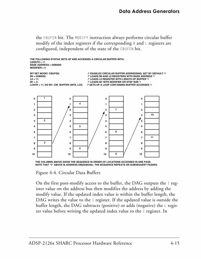
ADSP-2126x SHARC Processor Hardware Reference 4-15
Data Address Generators
the CBUFEN bit. The MODIFY instruction always performs circular buffer modify of the index registers if the corresponding B and L registers are configured, independent of the state of the CBUFEN bit.
On the first post-modify access to the buffer, the DAG outputs the I reg-ister value on the address bus then modifies the address by adding the modify value. If the updated index value is within the buffer length, the DAG writes the value to the I register. If the updated value is outside the buffer length, the DAG subtracts (positive) or adds (negative) the L regis-ter value before writing the updated index value to the I register. In
Figure 4-4. Circular Data Buffers
0
1
2
3
4
5
6
7
8
9
10
1
2
3
0
1
2
3
4
5
6
7
8
9
10
4
5
6
0
1
2
3
4
5
6
7
8
9
10
7
8
9
0
1
2
3
4
5
6
7
8
9
10
10
11
THE COLUMNS ABOVE SHOW THE SEQUENCE IN ORDER OF LOCATIONS ACCESSED IN ONE PASS.NOTE THAT "0" ABOVE IS ADDRESS DM(0X80500). THE SEQUENCE REPEATS ON SUBSEQUENT PASSES.
THE FOLLOWING SYNTAX SETS UP AND ACCESSES A CIRCULAR BUFFER WITH:LENGTH = 11BASE ADDRESS = 0X80500MODIFIER = 4
BIT SET MODE1 CBUFEN; /* ENABLES CIRCULAR BUFFER ADDRESSING; SET BY DEFAULT */B0 = 0X80500; /* LOADS B0 AND L0 REGISTERS WITH BASE ADDRESS */L0 = 11; /* LOADS L0 REGISTER WITH LENGTH OF BUFFER */M1 = 4; /* LOADS M1 WITH MODIFIER OR STEP SIZE */LCNTR = 11, DO MY_CIR_BUFFER UNTIL LCE; /* SETS UP A LOOP CONTAINING BUFFER ACCESSES */

DAG Operations
4-16 ADSP-2126x SHARC Processor Hardware Reference
equation form, these post-modify and wraparound operations work as follows.
• If M is positive:
Inew = Iold + M if Iold + M < buffer base (start of buffer)
Inew = Iold + M – L if Iold + M ≥ buffer base + length (end of buffer)
• If M is negative:
Inew = Iold + M if Iold + M ≥ buffer base (start of buffer)
Inew = Iold + M + L if Iold + M < buffer base (start of buffer)
The DAGs use all four types of DAG registers for addressing circular buf-fers. These registers operate as follows for circular buffering.
• The index (I) register contains the value that the DAG outputs on the address bus.
• The modify (M) register contains the post-modify amount (positive or negative) that the DAG adds to the I register at the end of each memory access. The M register can be any M register in the same DAG as the I register and does not have to have the same number. The modify value can also be an immediate value instead of an M register. The size of the modify value, whether from an M register or immediate, must be less than the length (L register) of the circular buffer.
• The length (L) register sets the size of the circular buffer and the address range that the DAG circulates the I register through. The L register must be positive and cannot have a value greater than 231 – 1. If an L register’s value is zero, its circular buffer operation is disabled.

ADSP-2126x SHARC Processor Hardware Reference 4-17
Data Address Generators
• The DAG compares the base (B) register, or the B register plus the L register, to the modified I value after each access. When the B regis-ter is loaded, the corresponding I register is simultaneously loaded with the same value. When I is loaded, B is not changed. Programs can read the B and I registers independently.
There is one set of registers (I7 and I15) in each DAG that can generate an interrupt on circular buffer overflow (address wraparound). For more information, see “Using DAG Status” on page 4-9.
When a program needs to use I7 or I15 without circular buffering and the DSP has the circular buffer overflow interrupts unmasked, the program should disable the generation of these interrupts by setting the B7/B15 and L7/L15 registers to values that prevent the interrupts from occurring. If I7 were accessing the address range 0x1000 – 0x2000, the program could set B7 = 0x0000 and L7 = 0xFFFF. Because the DSP generates the circular buffer interrupt based on the wraparound equations on page 4-16, setting the L register to zero does not necessarily achieve the desired results. If the program is using either of the circular buffer overflow interrupts, it should avoid using the corresponding I register(s) (I7 or I15) where interrupt branching is not needed.
There are two special cases to be aware of when using circular buffers.
1. In the case of circular buffer overflow interrupts, if CBUFEN = 1 and register L7 = 0 (or L15 = 0), the CB7I (or CB15I) interrupt occurs at every change of I7 (or I15) after the index register (I7 or I15) crosses the base register (B7 or B15) value. This behavior is indepen-dent of the context of the DAG registers, both primary and alternate.
2. When a LW access, SIMD access, or normal word access with the LW option crosses the end of the circular buffer, the processor completes the access before responding to the end of buffer condition.

DAG Operations
4-18 ADSP-2126x SHARC Processor Hardware Reference
Modifying DAG RegistersThe DAGs support two operations that modify an address value in an index register without outputting an address. These two operations, address bit-reversal and address modify, are useful for bit-reverse address-ing and maintaining pointers.
The MODIFY instruction modifies addresses in any DAG index register (I0-I15) without accessing memory. If the I register’s corresponding B and L registers are set up for circular buffering, a MODIFY instruction performs the specified buffer wraparound (if needed). The syntax for MODIFY is sim-ilar to post-modify addressing (index, then modifier). The MODIFY instruction accepts either a 32-bit immediate value or an M register as the modifier. The following example adds 4 to I1 and updates I1 with the new value:MODIFY(I1,4);
The BITREV instruction modifies and bit-reverses addresses in any DAG index register (I0-I15) without accessing memory. This instruction is independent of the bit-reverse mode. The BITREV instruction adds a 32-bit immediate value to a DAG index register, bit-reverses the result, and writes the result back to the same index register. The following example adds 4 to I1, bit-reverses the result, and updates I1 with the new value:BITREV(I1,4);
Addressing in SISD and SIMD ModesSingle-Instruction, Multiple-Data (SIMD) mode (PEYEN bit=1) does not change the addressing operations in the DAGs, but it does change the amount of data that moves during each access. The DAGs put the same addresses on the address buses in SIMD and Single-Instruction Sin-gle-Data (SISD) modes. In SIMD mode, the DSP’s memory and processing elements get data from the named (explicit) locations in the instruction syntax as well as complementary (implicit) locations. For more

ADSP-2126x SHARC Processor Hardware Reference 4-19
Data Address Generators
information on data moves between registers, see “SIMD (Computa-tional) Operations” on page 2-49.
DAGs, Registers, and MemoryDAG registers are part of the DSP’s universal register (Ureg) set. Programs may load the DAG registers from memory, from another universal regis-ter, or with an immediate value. Programs may store DAG registers’ contents to memory or to another universal register.
The DAG’s registers support the bidirectional register-to-register transfers that are described in “SIMD (Computational) Operations” on page 2-49. When the DAG register is a source of the transfer, the destination can be a register file data register. This transfer results in the contents of the single source register being duplicated in complementary data registers in each processing element.
Programs should use care in the case where the DAG register is a destina-tion of a transfer from a register file data register source. Programs should use a conditional operation to select either one processing element or nei-ther as the source. Having both processing elements contribute a source value results in the PEx element’s write having precedence over the PEy element’s write.
In the case where a DAG register is both source and destination, the data move operation executes the same as it would if SIMD mode were dis-abled (PEYEN cleared).
DAG Register-to-Bus AlignmentThere are three word alignment types for DAG registers and PM or DM data buses: normal word, extended-precision normal word, and long word.

DAGs, Registers, and Memory
4-20 ADSP-2126x SHARC Processor Hardware Reference
The DAGs align normal word (32-bit) addressed transfers to the low order bits of the buses. These transfers between memory and 32-bit DAG1 or DAG2 registers use the 64-bit DM and PM data buses. Figure 4-5 illus-trates these transfers.
The DAGs align extended-precision normal word (40-bit) addressed transfers or register-to-register transfers to bits 39-8 of the buses. These transfers between a 40-bit data register and 32-bit DAG1 or DAG2 regis-ters use the 64-bit DM and PM data buses. Figure 4-6 illustrates these transfers.
Long word (64-bit) addressed transfers between memory and 32-bit DAG1 or DAG2 registers target double DAG registers and use the 64-bit DM and PM data buses. Figure 4-7 illustrates how the bus works in these transfers.
If the long word transfer specifies an even numbered DAG register (I0 or I2), then the even numbered register value transfers on the lower half of
Figure 4-5. Normal Word (32-bit) DAG Register Memory Transfers
Figure 4-6. DAG Register-to-Data Register Transfers
DAG1 OR DAG2 REGISTERS
031630X0000 0000
DM OR PM DATA BUS
031
DAG1 OR DAG2 REGISTERS
039
039630X0000 00
DM OR PM DATA BUS
0X008

ADSP-2126x SHARC Processor Hardware Reference 4-21
Data Address Generators
the 64-bit bus, and the even numbered register + 1 value transfers on the upper half (bits 63-32) of the bus.
If the long word transfer specifies an odd numbered DAG register (I1 or B3), the odd numbered register value transfers on the lower half of the 64-bit bus, and the odd numbered register – 1 value (I0 or B2 in this example) transfers on the upper half (bits 63-32) of the bus.
In both the even and odd numbered cases, the explicitly specified DAG register sources or sinks bits 31-0 of the long word addressed memory.
For implicit moves and long word accesses that use the PX registers, as for example:
I0 = PX; equates to I0 = PX1;
only the contents of the PX1 register are written into I0. However, the fol-lowing example:
PX = I0; equates to PX1 = PX2 = I0;.
DAG Register Transfer RestrictionsThe two types of transfer restrictions are hold-off conditions and illegal conditions that the DSP does not detect.
Figure 4-7. Long Word DAG Register-to-Data Register Transfers
EXPLICIT (NAMED)DAG1 OR DAG2 REGISTERS
031
31 063
DM OR PM DATA BUS
IMPLICIT (NAMED + OR - 1)DAG1 OR DAG2 REGISTERS
031

DAGs, Registers, and Memory
4-22 ADSP-2126x SHARC Processor Hardware Reference
For certain instruction sequences involving transfers to and from DAG registers, an extra (NOP) cycle is automatically inserted by the processor. In case where an instruction that loads a DAG register is followed by an
instruction that uses any register in the same DAG register pair1 for data addressing, modify instructions, or indirect jumps, the DSP inserts an extra (NOP) cycle between the two instructions. This hold-off occurs because the same bus is needed by both operations in the same cycle. Therefore, the second operation must be delayed. The following example causes a delay because it exhibits a write/read dependency in which I0 is written in one cycle. The results of that register write are not available to a register read for one cycle. Note that if either instruction had specified I1, the stall occurs only if the first instruction performs a long word (LW) access. The DAG detects write/read dependencies with a register pair granularity:I0 = 8;
DM(I0,M1) = R1;
Certain sequences of instructions cause incorrect results on the DSP and are flagged as errors by the DSP assembler software. The following types of instructions can execute on the processor, but cause incorrect results.
• An instruction that stores a DAG register in memory using indirect addressing from the same DAG, with or without an update of the index register. The instruction writes the wrong data to memory or updates the wrong index register.
Do not try these: DM(M2,I1) = I0; or DM(I1,M2) = I0;These example instructions do not work because I0 and I1 are both DAG1 registers.
1 DAG registers are accessible in pair granularity for single cycle access. The pairings are odd-even. For example I0 and I1 are a pair, and I2 and I3 are a pair.

ADSP-2126x SHARC Processor Hardware Reference 4-23
Data Address Generators
• An instruction that loads a DAG register from memory using indi-rect addressing from the same DAG, with an update of the index register. The instruction either loads the DAG register or updates the index register, but not both.
Do not try this: L2 = DM(I1,M0);This example instruction does not work because L2 and I1 are both DAG1 registers.
DAG Instruction SummaryTable 4-2, Table 4-3, Table 4-4, Table 4-5, Table 4-6, Table 4-7, Table 4-8, and Table 4-9 list the DAG instructions. For more information on assembly language syntax, see the ADSP-21160 SHARC DSP Instruc-tion Set Reference.
In these tables, note the meaning of the following symbols:
• I15–8 indicates a DAG2 index register: I15, I14, I13, I12, I11, I10, I9, or I8, and I7–0 indicates a DAG1 index register I7, I6, I5, I4, I3, I2, I1, or I0.
• M15–8 indicates a DAG2 modify register: M15, M14, M13, M12, M11, M10, M9, or M8, and M7–0 indicates a DAG1 modify register M7, M6, M5, M4, M3, M2, M1, or M0.
• Ureg indicates any universal register; for a list of the DSP’s univer-sal registers, see Table A-1 on page A-3.
• Dreg indicates any data register; for a list of the DSP’s data regis-ters, see the Data Register File registers listed in Table A-1 on page A-3.
• Data32 indicates any 32-bit value, and Data6 indicates any 6-bit value.

DAG Instruction Summary
4-24 ADSP-2126x SHARC Processor Hardware Reference
Table 4-2. Post-Modify Addressing, Modified by M Register and Updating I Register
DM(I7–0,M7–0)=Ureg (LW); {DAG1}
PM(I15–8,M15–8)=Ureg (LW); {DAG2}
Ureg=DM(I7–0,M7–0) (LW); {DAG1}
Ureg=PM(I15–8,M15–8) (LW); {DAG2}
DM(I7–0,M7–0)=Data32; {DAG1}
PM(I15–8,M15–8)=Data32; {DAG2}
Table 4-3. Post-Modify Addressing, Modified by 6-bit Data and Updating I Register
DM(I7–0,Data6)=Dreg; {DAG1}
PM(I15–8,Data6)=Dreg; {DAG2}
Dreg=DM(I7–0,Data6); {DAG1}
Dreg=PM(I15–8,Data6); {DAG2}
Table 4-4. Pre-Modify Addressing, Modified by M Register (No I Register Update)
DM(M7–0,I7–0)=Ureg (LW); {DAG1}
PM(M15–8,I15–8)=Ureg (LW); {DAG2}
Ureg=DM(M7–0,I7–0) (LW); {DAG1}
Ureg=PM(M15–8,I15–8) (LW); {DAG2}

ADSP-2126x SHARC Processor Hardware Reference 4-25
Data Address Generators
Table 4-5. Pre-Modify Addressing, Modified by 6-bit Data (No I Register Update)
DM(Data6,I7–0)=Dreg; {DAG1}
PM(Data6,I15–8)=Dreg; {DAG2}
Dreg=DM(Data6,I7–0); {DAG1}
Dreg=PM(Data6,I15–8); {DAG2}
Table 4-6. Pre-Modify Addressing, Modified by 32-bit Data (No I Register Update)
Ureg=DM(Data32,I7–0) (LW); {DAG1}
Ureg=PM(Data32,I15–8) (LW); {DAG2}
DM(Data32,I7–0)=Ureg (LW); {DAG1}
PM(Data32,I15–8)=Ureg (LW); {DAG2}
Table 4-7. Update (Modify) I Register, Modified by M Register
Modify(I7–0,M7–0); {DAG1}
Modify(I15–8,M15–8); {DAG2}
Table 4-8. Update (Modify) I Register, Modified by 32-bit Data
Modify(I7–0,Data32); {DAG1}
Modify(I15–8,Data32); {DAG2}
Table 4-9. Bit-Reverse and Update I Register, Modified By 32-Bit Data
Bitrev(I7–0,Data32); {DAG1}
Bitrev(I15–8,Data32); {DAG2}
DAG Instruction Summary
4-26 ADSP-2126x SHARC Processor Hardware Reference

ADSP-2126x SHARC Processor Hardware Reference 5-1
5 MEMORY
The ADSP-2126x contains a large, dual-ported internal memory for single cycle, simultaneous, independent accesses by the core processor and I/O processor. The dual-ported memory, in combination with three separate on-chip buses, allow two data transfers from the core and one transfer from the I/O processor in a single cycle. Using the I/O bus, the I/O pro-cessor provides data transfers between internal memory and the DSP’s communication ports (serial ports and parallel port) without hindering the DSP core’s access to memory. This chapter describes the DSP’s memory and how to use it.
The DSP contains up to 2M bits of internal RAM and up to 4M bits of
internal ROM depending on the specific part number1. Regardless, each block can be configured for different combinations of code and data stor-age. All of the memory can be accessed as 16-bit, 32-bit, 48-bit, or 64-bit words. The DSP features a 16-bit floating-point storage format that effec-tively doubles the amount of data that may be stored on-chip. A single instruction converts the format from 32-bit floating-point to 16-bit floating-point.
While each memory block can store combinations of code and data, accesses are most efficient when one block stores data using the DM bus, (typically block 1) for transfers, and the other block (typically block 0) stores instructions and data using the PM bus. Using the DM bus and PM bus with one dedicated to each memory block assures single-cycle execu-tion with two data transfers. In this case, the instruction must be available in the cache.
1 For specific memory information, see your ADSP-2126x product specific data sheet.

Internal Memory
5-2 ADSP-2126x SHARC Processor Hardware Reference
Internal MemoryThe ADSP-21262 and ADSP-21266 SHARC DSPs contain 2M bits of internal RAM and 4M bits of internal ROM. Block 0 has 1M bit RAM and 2M bits ROM. Block 1 has 1M bit RAM and 2M bits ROM. Table 5-1 shows the maximum number of data or instruction words that can fit in each internal memory block.
The ADSP-2126x family members are available with varying amounts of internal ROM and RAM. For a complete list, visit our web site at www.analog.com\SHARC.
DSP ArchitectureMost microprocessors use a single address and a single-data bus for mem-ory accesses. This type of memory architecture is referred to as the Von Neumann architecture. Because DSPs require greater data throughput
Table 5-1. Words Per Internal Memory Block (ADSP-21262/21266 Models)
Word Type Bits Per Word
Maximum Number of Words in Block 0
Maximum Number of Words in Block 1
1M bit RAM 2M bits ROM 1M bit RAM 2M bits ROM
Instruction 48 bits 21.33K words 42K words 21.33K words 42K words
Long Word Data
64 bits 16K words 32K words 16K words 32K words
Extended-PrecisionNormal Word Data
40 bits 21.33K words 42K words 21.33K words 42K words
Normal Word Data
32 bits 32K words 64K words 32K words 64K words
Short Word Data
16 bits 64K words 128K words 64K words 128K words

ADSP-2126x SHARC Processor Hardware Reference 5-3
Memory
than the Von Neumann architecture provides, many DSPs use memory architectures that have separate data and address buses for program and data storage. These two sets of buses let the DSP retrieve a data word and an instruction simultaneously. This type of memory architecture is called Harvard architecture.
SHARC DSPs go a step further by using a Super Harvard architecture. This four bus architecture has two address buses and two data buses, but provides a single, unified address space for program and data storage. While the Data Memory (DM) bus only carries data, the Program Mem-ory (PM) bus handles instructions and data, allowing dual-data accesses.
Processor core and I/O processor accesses to internal memory are completely independent and transparent to one another. Each block of memory can be accessed by the DSP core and I/O proces-sor in every cycle—no extra cycles are incurred if the DSP core and the I/O processor access the same block.
A memory access conflict can occur when the processor core attempts two accesses to the same internal memory block in the same cycle. When this conflict, known as a block conflict occurs, an extra cycle is incurred. The DM bus access completes first and the PM bus access completes in the fol-lowing (extra) cycle.
For more information on how the buses access memory blocks, see “Inter-nal Memory” on page 5-2.
BusesAs shown in Figure 5-1, the processor has three sets of internal buses con-nected to its dual-ported memory, the Program Memory (PM), Data Memory (DM), and I/O Processor (I/O) buses. The PM and DM buses share one memory port and the I/O bus connects to the other port. Mem-ory accesses from the DSP’s core (computational units, data address generators, or program sequencer) use the PM or DM buses, while the I/O

Buses
5-4 ADSP-2126x SHARC Processor Hardware Reference
processor uses the I/O bus for memory accesses. The I/O processor’s par-allel port (PP) bus can access external memory devices.
Internal Address and Data BusesFigure 5-1 on page 5-5 shows that the PM and DM buses have access to internal memory.
The DSP’s DM and PM buses can access internal memory independently. The I/O processor can perform DMA between external and internal mem-ory without conflicts with the DM and PM buses.
Addresses for the PM and DM buses come from the DSP’s program sequencer and Data Address Generators (DAGs). The program sequencer generates 24-bit program memory addresses while DAGs supply 32-bit addresses for locations throughout the DSP’s memory spaces. The DAGs supply addresses for data reads and writes on both the PM and DM address buses, while the program sequencer uses only the PM address bus for sequencing execution.
Each DAG is associated with a particular data bus. DAG1 supplies addresses over the DM bus and DAG2 supplies addresses over the PM bus. For more information on address generation, see Chapter 3, Program Sequencer or Chapter 4, Data Address Generators.

ADSP-2126x SHARC Processor Hardware Reference 5-5
Memory
Figure 5-1. ADSP-21262 Processor Memory and Internal Buses Block Diagram
ADDRESS DATAADDRESS DATA
ADDRESS
DATA
ADDRESS
DATA
PX BUS EXCHANGE REGISTER
PM ADDRESS BUS
PM DATA BUS
DM ADDRESS BUS
DM DATA BUS
IO ADDRESS BUS
IO DATA BUS
ANY TWO PATHSSIMULTANEOUSLY
ADDRESSES ANDDATA FOLLOW
PARALLEL PATHS
IO ADDRESS
IO DATA
ADDRESS DATA
PARALLEL PORT
AD
BLOCK 0
BLOCK 1
INTERNAL(DSP) MEMORY
EXTERNAL(SYSTEM) MEMORY
I/O PROCESSOR
32 32 64 64 3224/16
64
16
19

Buses
5-6 ADSP-2126x SHARC Processor Hardware Reference
Because the DSP’s internal memory is arranged in four 16-bit wide by 96K columns, memory is addressable in widths that are multiples of col-umns up to 64 bits:
1 column = 16-bit words
2 columns = 32-bit words
3 columns = 48- or 40-bit words
4 columns = 64-bit words
For more information on the how the DSP works with memory words, see “Memory Organization and Word Size” on page 5-12.
The PM and DM data buses are 64 bits wide. Both data buses can handle long word (64-bit), normal word (32-bit), Extended-precision normal word (40-bit), and short word (16-bit) data, but only the PM data bus carries instruction words (48-bit).
Internal Data Bus ExchangeThe data buses allow programs to transfer the contents of any register in the DSP to any other register or to any internal memory location in a sin-gle cycle. As shown in Figure 5-2, the PM Bus Exchange (PX) register permits data to flow between the PM and DM data buses. The PX register can work as one 64-bit register or as two 32-bit registers (PX1 and PX2). The alignment of PX1 and PX2 within PX appears in Figure 5-2.
The PX1, PX2, and the combined PX registers are Universal registers (Ureg) that are accessible for register-to-register or memory-to-register transfers.
The PX register-to-register transfers using data registers are either 40-bit transfers for the combined PX or 32-bit transfers for PX1 or PX2. Figure 5-2 shows the bit alignment and gives an example of instructions for regis-ter-to-register transfers.

ADSP-2126x SHARC Processor Hardware Reference 5-7
Memory
Figure 5-2 shows that during a transfer between PX1 or PX2 and a data reg-ister (Dreg), the bus transfers the upper 32 bits of the register file and zero-fills the eight least significant bits (LSBs).
During a transfer between the combined PX register and a register file, the bus transfers the upper 40 bits of PX and zero-fills the lower 24 bits.
Figure 5-2. PM Bus Exchange (PX, PX1, and PX2) Registers
Figure 5-3. PX, PX1, and PX2 Register-to-Register Transfers
PX1
03263
PX2
31
0031 31
Combined PX RegisterInstruction Examples
PX = DM(0x80000)(LW);PX = DM(0x40000);
Register File Transfer
PX1 or PX2
39 7 0
0x0
32 bits
Register File Transfer
39 0
40 bits 0x0
02363
8
32 bits
31 024
40 bits
Combined PX
PX1PX2
Instruction Examples
R3 = PX; R3 = PX1; or R3 = PX2;

Buses
5-8 ADSP-2126x SHARC Processor Hardware Reference
The PX register-to-internal memory transfers over the DM or PM data bus are either 48-bit transfers for the combined PX or 32-bit transfers (on bits 31-0 of the bus) for PX1 or PX2. Figure 5-5 shows these transfers.
Figure 5-5 shows that during a transfer between PX1 or PX2 and internal memory, the bus transfers the lower 32 bits of the register.
During a transfer between the combined PX register and internal memory, the bus transfers the upper 48 bits of PX and zero-fills the lower 8 bits.
The status of the memory block’s Internal Memory Data Width (IMDWX) setting does not effect this default transfer size for PX to internal memory.
All transfers between the PX register (or any other internal register or memory) and any I/O processor register are 32-bit transfers (least signifi-cant 32 bits of PX).
Figure 5-4. PX, PX1, PX2 Register-to-Memory Transfers on DM (LW) or PM (LW) Data Bus
Instruction Examples
PX = DM (0xC0000) (LW); PM(I7,M7) = PX1;
31
PX1 or PX2
32 bits
063
0x0 32 bits
DM or PM Data Bus Transfer
31 0
7
PX2
DM and PM Data Bus Transfer (not LW)
03163
48 bits
8
7 03163 8
48 bits 0x0
0x0
PX1
Combined PX

ADSP-2126x SHARC Processor Hardware Reference 5-9
Memory
All transfers between the PX register and data registers (R0–R15 or S0–S15) are 40-bit transfers. The most significant 40 bits are transferred as shown in Figure 5-3 on page 5-7.
Figure 5-5 shows the transfer size between PX and internal memory over the PM or DM data bus when using the long word (LW) option.
The LW notation in Figure 5-5 shows an important feature of PX regis-ter-to-internal memory transfers over the PM or DM data bus for the combined PX register. The PX register transfers to memory are 48-bit (three column) transfers on bits 63-16 of the PM or DM data bus, unless forced to be 64-bit (four column) transfers with the LW (long word) mnemonic.
There is no implicit move when the combined PX register is used in SIMD mode. For example, in SIMD mode, the following moves occur:
Figure 5-5. PX Register-to-Memory Transfers on PM Data Bus
Combined PX
DM (LW) or PM (LW)
03163
64 bits
03163
64 bits
Data Bus Transfer
Instruction Example PX = PM (0x80000)LW;

ADSP-2126x Memory Map
5-10 ADSP-2126x SHARC Processor Hardware Reference
PX1 = R0; /* R0 32-bit explicit move to PX1,
and S0 32-bit implicit move to PX2 */
PX = R0; /* R0 40-bit explicit move to PX,
but no implicit move for S0 */
ADSP-2126x Memory MapThe ADSP-2126x family is composed of a variety of models that have varying amounts of RAM and/or ROM memory. However, in general, there are two memory spaces: internal memory space and external (DMA) memory space. These spaces have these definitions:
• Internal memory space. This space ranges from address 0x00 0000 through 0x1F FFFF. Internal memory space refers to the DSP’s on-chip RAM, on-chip ROM, and memory-mapped registers.
• External (DMA) memory. For information on external DMA memory space please refer to the product specific data sheet.
Figure 5-6. PX Register-to-Internal Memory Transfers Over the PM or DM DATA Bus
USTAT1
03163
64 bits
03163
64 bits
Instruction Example
PX = USTAT1;
03163
64 bits
03163
64 bits
USTAT2
PX2PX1

ADSP-2126x SHARC Processor Hardware Reference 5-11
Memory
The ADSP-2126x has two blocks of RAM that contain up to 1M bit of memory each, and two blocks of ROM that contain up to 2M bits of memory each. Each block is physically comprised of four 16-bit columns. “Wrapping”, as shown in Figure 5-8 on page 5-14, allows the memory to efficiently store 16-bit, 32-bit, 48-bit or 64-bit wide words. The width of the data word fetched from memory is dependant upon the address range used. The same physical location in memory can be accessed using three different addresses.
Accessing a short word memory address accesses one 16-bit word. Consec-utive 16-bit short-words are accessed from columns #1, #2, #3, #4, #1 and so on. Accessing a normal word memory address transfers 32 bits (from columns 1 and 2 or 3 and 4). Consecutive 32-bit words are accessed from columns 1 and 2, 3 and 4, 1 and 2 etc. Accessing a long word address transfers 64 bits (from all four columns). For example, the same 16 bits of Block-0 are overwritten in each of the following four write instructions (some, but not all of the short word accesses overwrite more than 16 bits).
Listing 5-1. Overwriting Bits (ADSP-21262 Example)
#include <def2126x.h>
DM(0x00040000) = PX; /* long word transfer
(64 bits/four columns) */DM(0x00080000) = R0; /* normal word transfer
(32 bits/two columns) */DM(0x00100000) = R0; /* short word transfer
(16 bits/1-column) */NOP
USTAT1 = dm(SYSCTL);
bit set USTAT1 IMDW0; /* set Blk0 access as ext. precision */dm(SYSCTL) = USTAT1;
DM(0x00080000) = R0; /* normal word transfer
(40 bits/three columns) */

ADSP-2126x Memory Map
5-12 ADSP-2126x SHARC Processor Hardware Reference
Normal word address space is also used by the program sequencer to fetch 48-bit instructions. Note that a 48-bit fetch spans three columns that can lead to a different address range between instruc-tion fetches and data fetches (Figure 5-7).
Normal word address space can also optionally be used to fetch 40-bit data (from three columns) if the IMDWx (Internal Memory Data Width) bit in the SYSCTL register is set. There are two bits in the SYSCTL register, IMDW0 and IMDW1, which determine whether access to each block is 32 or 40 bits. For more information, see “Accessing Memory” on page 5-22.
The I/O processor’s memory-mapped registers control the system configu-ration of the DSP and I/O operations. For information about the I/O Processor, see Chapter 7, I/O Processor. These registers occupy consecu-tive 32-bit locations in this region.
If a program uses long word addressing (forced with the LW mnemonic) to access this region, the access is only to the addressed 32-bit register, rather than the two adjacent I/O processor registers. The register contents are transferred on bits 31–0 of the data bus.
Memory Organization and Word SizeThe DSP’s internal memory is organized as four 16-bit wide by 64K high columns. These columns of memory are addressable as a variety of word sizes:
• 64-bit long word data (four columns)
• 48-bit instruction words or 40-bit extended-precision normal word data (3 columns)

ADSP-2126x SHARC Processor Hardware Reference 5-13
Memory
• 32-bit normal word data (2 columns)
• 16-bit short word data (1 column)
Extended-precision normal word data is only accessible if the IMDWx bit is set in the SYSCTL register. It is left-justified within a three col-umn location, using bits 47–8 of the location.
Placing 32-Bit Words and 48-Bit Words
When the processor core or I/O processor addresses memory, the word width of the access determines which columns within the memory are accessed. For instruction word (48 bits) or extended-precision normal word data (40 bits), the word width is 48 bits, and the DSP accesses the memory’s 16-bit columns in groups of three. Because these sets of three column accesses are packed into a 4 column matrix, there are four rota-tions of the columns for storing 40- or 48-bit data. The three column word rotations within the four column matrix appear in Figure 5-7.
For long word (64 bits), normal word (32 bits), and short word (16 bits) memory accesses, the DSP selects from fixed columns in memory. No rotations of words within columns occur for these data types.
Figure 5-7. 48-Bit Word Rotations
Column 0Column 1Column 2Column 3150
Rotation 2
Ad
dre
sses
Rotation 3 Rotation 2
Rotation 1
Rotation 1 Rotation 0
150150150

ADSP-2126x Memory Map
5-14 ADSP-2126x SHARC Processor Hardware Reference
Figure 5-8 shows the memory ranges for each data size in the DSP’s inter-nal memory.
Mixing 32-Bit Words and 48-Bit Words
The DSP’s memory organization lets programs freely place memory words of all sizes (see “Memory Organization and Word Size” on page 5-12) with few restrictions (see “Restrictions on Mixing 32-Bit Words and 48-Bit Words” on page 5-16). This memory organization also lets pro-grams mix (place in adjacent addresses) words of all sizes. This section discusses how to mix odd (three-column) and even (four-column) data words in the DSP’s memory.
Transition boundaries between 48-bit (three-column) data and any other data size can occur only at any 64-bit address boundary within either internal memory block. Depending on the ending address of the 48-bit words, there are zero, one, or two empty locations at the transition between the 48-bit (three-column) words and the 64-bit (four-column) words. These empty locations result from the column rotation for storing
Figure 5-8. Mixed Instructions and Data With No Unused Locations
Column 0Column 1Column 2Column 3150150150150
48-bit word top-348-bit word top-2
48-bit word top-248-bit word top-1
48-bit word top-148-bit word top
Ad
dre
sses
Transitioning from 48-bit to 32-bit data with zero empty locations:
(48-bit word top address)
32-bit word 232-bit word 3
32-bit word 032-bit word 1
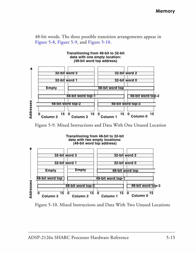
ADSP-2126x SHARC Processor Hardware Reference 5-15
Memory
48-bit words. The three possible transition arrangements appear in Figure 5-8, Figure 5-9, and Figure 5-10.
Figure 5-9. Mixed Instructions and Data With One Unused Location
Figure 5-10. Mixed Instructions and Data With Two Unused Locations
Column 0Column 1Column 2Column 3150150150150
48-bit word topEmpty
48-bit word top-1 48-bit word top-2
48-bit word top-2 48-bit word top-3
Ad
dre
sses
32-bit word 232-bit word 3
32-bit word 032-bit word 1
Transitioning from 48-bit to 32-bit data with one empty location:
(48-bit word top address)
Column 0Column 1Column 2Column 3150150150150
48-bit word topEmpty
48-bit word top-148-bit word top
48-bit word top-2
32-bit word 232-bit word 3
32-bit word 032-bit word 1
Transitioning from 48-bit to 32-bit data with two empty locations:
(48-bit word top address)
Empty
48-bit word top-3
Ad
dre
sses

ADSP-2126x Memory Map
5-16 ADSP-2126x SHARC Processor Hardware Reference
Restrictions on Mixing 32-Bit Words and 48-Bit Words
There are some restrictions that stem from the memory column rotations for three-column data (48- or 40-bit words) and they relate to the way that three-column data can mix with four-column data (32-bit words) in memory. These restrictions apply to mixing 48- and 32-bit words, because the DSP uses a normal word address to access both of these types of data even though 48-bit data maps onto three columns of memory and 32-bit data maps onto two columns of memory.
When a system has a range of three-column (48-bit) words followed by a range of two-column (32-bit) words, there is often a gap of empty 16-bit locations between the two address ranges. The size of the address gap var-ies with the ending address of the range of 48-bit words. Because the addresses within the gap alias to both 48- and 32-bit words, a 48-bit write into the gap corrupts 32-bit locations, and a 32-bit write into the gap cor-rupts 48-bit locations. The locations within the gap are only accessible with short word (16-bit) accesses.
Calculating the starting address for four column data that minimizes the gap after three column data is useful for programs that are mixing three and four column data. Given the last address of the three column (48-bit) data, the starting address of the 32-bit range that most efficiently uses memory can be determined by the equation shown in Listing 5-2.
Listing 5-2. Starting Address
m = B + 2 [(n MOD K) – TRUNC (n MOD K) / 4)]
where:
• K is 21844 for RAM and 43690 for ROM
• n is the number of contiguous 48-bit words allocated in the inter-nal memory block (n < 43,690 for ROM, n < 21844 for RAM)
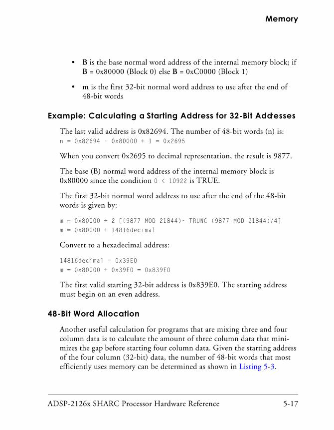
ADSP-2126x SHARC Processor Hardware Reference 5-17
Memory
• B is the base normal word address of the internal memory block; if B = 0x80000 (Block 0) else B = 0xC0000 (Block 1)
• m is the first 32-bit normal word address to use after the end of 48-bit words
Example: Calculating a Starting Address for 32-Bit Addresses
The last valid address is 0x82694. The number of 48-bit words (n) is:n = 0x82694 - 0x80000 + 1 = 0x2695
When you convert 0x2695 to decimal representation, the result is 9877.
The base (B) normal word address of the internal memory block is 0x80000 since the condition 0 < 10922 is TRUE.
The first 32-bit normal word address to use after the end of the 48-bit words is given by:
m = 0x80000 + 2 [(9877 MOD 21844)- TRUNC (9877 MOD 21844)/4]
m = 0x80000 + 14816decimal
Convert to a hexadecimal address:
14816decimal = 0x39E0
m = 0x80000 + 0x39E0 = 0x839E0
The first valid starting 32-bit address is 0x839E0. The starting address must begin on an even address.
48-Bit Word Allocation
Another useful calculation for programs that are mixing three and four column data is to calculate the amount of three column data that mini-mizes the gap before starting four column data. Given the starting address of the four column (32-bit) data, the number of 48-bit words that most efficiently uses memory can be determined as shown in Listing 5-3.

ADSP-2126x Memory Map
5-18 ADSP-2126x SHARC Processor Hardware Reference
Listing 5-3. 48-Bit Word Allocation
n = TRUNC{4[(m - B) / 2] / 3]} + B
where:
• m is the first 32-bit normal word address after the end of 48-bit words (1m values falls in the valid normal word address space)
• B is the base normal word address of the internal memory block; B = 0x80000 (block 0) else B = 0xC0000 (block 1) for valid m values
• n is the number of contiguous 48-bit words the system allocates in the internal memory block
Internal Interrupt Vector TableThe default location of the ADSP-2126x’s interrupt vector table (IVT) depends on the DSP’s booting mode. When the processor boots from an external source (EPROM, SPI port master or slave booting), the vector table starts at address 0x0008 0000 (normal word). When the processor is in “no boot” mode (runs from internal ROM location 0x000A 0000 with-out loading), the interrupt vector table starts at address 0x000A–0000.
The Internal Interrupt Vector Table (IIVT) bit in the SYSCTL register over-rides the default placement of the vector table. If IIVT is set (=1), the interrupt table starts at address 0x0008 0000 (internal memory) regardless of the booting mode.
Internal Memory Data WidthThe DSP’s internal memory blocks use normal word addressing to access either single-precision 32-bit data or extended-precision 40-bit data. Pro-grams select the data width independently for each internal memory block

ADSP-2126x SHARC Processor Hardware Reference 5-19
Memory
using the Internal Memory Data Width (IMDWx) bits in the SYSCTL regis-ter. If a block’s IMDWx bit is cleared (=0), normal word accesses to the block access 32-bit data. If a block’s IMDWx bit is set (=1), normal word accesses to the block access 48-bit data. If a program tries to write 40-bit data (for example, a data register-to-memory transfer), the transfer truncates the lower 8 bits from the register; only writing 32 most significant bits.
If a program tries to read 40-bit data (for example, a memory-to-data reg-ister transfer), the transfer zero-fills the lower 8 bits of the register, only reading the 32 most significant bits (MSBs).
The Program Memory Bus Exchange (PX) register is the only exception to these transfer rules—all loads and or stores of the PX register are performed as 48-bit accesses unless forced to a 64-bit access with the LW mnemonic. If any 40-bit data must be stored in a memory block configured for 32-bit words, the program uses the PX register to access the 40-bit data in 48-bit words. Programs should take care not to corrupt any 32-bit data with this type of access. For more information, see “Restrictions on Mixing 32-Bit Words and 48-Bit Words” on page 5-16.
The Long word (LW) mnemonic only effects normal word address accesses and overrides all other factors (SIMD, IMDWx).
Secondary Processor Element (PEy)When the PEYEN bit in the MODE1 register is set (=1), the DSP is in Sin-gle-Instruction, Multiple-Data (SIMD) mode. In SIMD mode, many data access operations differ from the DSP’s default Single-Instruction, Sin-gle-Data (SISD) mode. These differences relate to doubling the amount of data transferred for each data access.
Accesses in SIMD mode transfer both an explicit (named) location and an implicit (unnamed, complementary) location. The explicit transfer is a data transfer between the explicit register and the explicit address, and the implicit transfer is between the implicit register and the implicit address.

ADSP-2126x Memory Map
5-20 ADSP-2126x SHARC Processor Hardware Reference
For information on complementary (implicit) registers in SIMD mode accesses, see “Secondary Processor Element (PEy)” on page 5-19. For more information on complementary (implicit) memory locations in SIMD mode accesses, see “Accessing Memory” on page 5-22.
Broadcast Register LoadsThe DSP’s BDCST1 and BDCST9 bits in the MODE1 register control broadcast register loading. When broadcast loading is enabled, the DSP writes to complementary registers or complementary register pairs in each process-ing element on writes that are indexed with DAG1 register I1 (if BDCST1 =1) or DAG2 register I9 (if BDCST9 =1). Broadcast load accesses are similar to SIMD mode accesses in that the DSP transfers both an explicit (named) location and an implicit (unnamed, complementary) location. However, broadcast loading only influences writes to registers and writes identical data to these registers. Broadcast mode is independent of SIMD mode.
Table 5-2 shows examples of explicit and implicit effects of broadcast reg-ister loads to both processing elements. Note that broadcast loading only effects loads of data registers (register file); broadcast loading does not effect register stores or loads to other system registers. Furthermore, broadcast loads only work on register loads; broadcast loading cannot be used for memory writes. For more information on broadcast loading, see “Accessing Memory” on page 5-22.
Table 5-2. Register Load Dual PE Broadcast Operation
Instruction
(Explicit, PEx Operation)1
1 The post increment in the explicit operation is performed before the implicit instructions are executed.
(Implicit, PEy operation)
Rx = dm(i1,ma);Rx = pm(i9,mb);Rx = dm(i1,ma), Ry = pm(i9,mb);
Sx = dm(i1,ma);Sx = pm(i9,mb);Sx = dm(i1,ma), Sy = pm(i9,mb);

ADSP-2126x SHARC Processor Hardware Reference 5-21
Memory
Illegal I/O Processor Register AccessThe DSP monitors I/O processor register access when the Illegal I/O pro-cessor Register Access (IIRAE) bit in the MODE2 register is set (=1). If access to the IOP registers is detected, an Illegal Input Condition Detected (IICDI) interrupt occurs. The interrupt is latched in the IRPTL register when a core access to an IOP register occurs.
The I/O processor’s DMA controller cannot generate the IICDI interrupt. For more information, see “Mode Control 2 Register (MODE2)” on page A-7.
Unaligned 64-Bit Memory AccessThe DSP monitors for unaligned 64-bit memory accesses if the Unaligned 64-bit Memory Accesses (U64MAE) bit in the MODE2 register (bit 21) is set (=1). An unaligned access is an odd numbered address normal word access that is forced to 64 bits with the LW mnemonic. When detected, this con-dition is an input that can cause an Illegal Input Condition Detected (IICDI) interrupt if the interrupt is enabled in the IMASK register. For more information, see “Mode Control 2 Register (MODE2)” on page A-7.
The following code example shows the access for even and odd addresses. When accessing an odd address, the sticky bit is set to indicate the unaligned access.bit set mode2 U64MAE; /* set testbit for aligned or
unaligned 64-bit access*/
r0 = 0x11111111;
r1 = 0x22222222;
pm(0x80200) = r0(lw); /* even address in 32-bit, access
is aligned */
pm(0x80201) = r0(lw); /* odd address in 32-bit, sticky
bit is set */

Using Memory Access Status
5-22 ADSP-2126x SHARC Processor Hardware Reference
Using Memory Access StatusAs described in “Illegal I/O Processor Register Access” on page 5-21 and “Unaligned 64-Bit Memory Access” on page 5-21, the DSP can provide illegal access information for long word or I/O register accesses. When these conditions occur, the DSP updates an illegal condition flag in a sticky status (STKYx) register. Either of these two conditions can also gen-erate a maskable interrupt. Two ways to use illegal access information are:
• Interrupts. Enable interrupts and use an interrupt service routine (ISR) to handle the illegal access condition immediately. This method is appropriate if it is important to handle all illegal accesses as they occur.
• STKYx registers. Sticky registers hold a value that can be checked for a specific condition at a later time. Use the Bit Tst instruction to examine illegal condition flags in the STKYx register after an interrupt to determine which illegal access condition occurred.
Accessing MemoryThe word width of DSP processor core accesses to internal memory include:
• 48-bit access for instruction words, extended-precision normal word (40-bit) data, and PX register
• 64-bit access for long word data, normal word (32-bit) data, or PX register data with the LW mnemonic
• 32-bit access for normal word (32-bit) data
• 16-bit access for short word data
The DSP determines whether a normal word access is 32 or 40 bits from the internal memory block’s IMDWx setting. For more information, see

ADSP-2126x SHARC Processor Hardware Reference 5-23
Memory
“Internal Memory Data Width” on page 5-18. While mixed accesses of 48-bit words and 16-, 32-, or 64-bit words at the same address are not allowed, mixed read/writes of 16-, 32-, and 64-bit words to the same address are allowed. For more information, see “Restrictions on Mixing 32-Bit Words and 48-Bit Words” on page 5-16.
The DSP’s DM and PM buses support 24 combinations of regis-ter-to-memory data access options. The following factors influence the data access type:
• Size of words—short word, normal word, extended-precision nor-mal word, or long word
• Number of words—single or dual-data move
• Mode of DSP—SISD, SIMD, or broadcast load
Access Word SizeThe DSP’s internal memory accommodates the following word sizes:
• 64-bit word data
• 48-bit instruction words
• 40-bit extended-precision normal word data
• 32-bit normal word data
• 16-bit short word data
Long Word (64-Bit) Accesses
A program makes a long word (64-bit) access to internal memory using an access to a long word address. Programs can also make a 64-bit access through normal word addressing with the LW mnemonic or through a PX register move with the LW mnemonic. The address ranges for internal memory accesses appear in the processor model data sheet.

Accessing Memory
5-24 ADSP-2126x SHARC Processor Hardware Reference
When data is accessed using long word addressing, the data is always long word aligned on 64-bit boundaries in internal memory space. When data is accessed using normal word addressing and the LW mnemonic, the pro-gram should maintain this alignment by using an even normal word address (least significant bit of address = 0). This register selection aligns the normal word address with a 64-bit boundary (long word address).
All long word accesses load or store two consecutive 32-bit data values. The register file source or destination of a long word access is a set of two neighboring data registers in a processing element. In a forced long word access (uses the LW mnemonic), the even (normal word address) location moves to or from the explicit register in the neighbor-pair, and the odd (normal word address) location moves to or from the implicit register in the neighbor-pair. For example, the following long word moves could occur:
DM(0x80000) = R0 (LW);
/* The data in R0 moves to location DM(0x80000), and the data in
R1 moves to location DM(0x80001) */
R0 = DM(0x80003)(LW);
/* The data at location DM(0x80002) moves to R0, and the data at
location DM(0x80003) moves to R1 */
The example shows that R0 and R1 are neighbor registers in the same pro-cessing element. Table 5-3 lists the other neighbor register assignments that apply to long word accesses.
In unforced long word accesses (accesses to LW memory space), the DSP places the lower 32 bits of the long word in the named (explicit) register and places the upper 32 bits of the long word in the neighbor (implicit) register.

ADSP-2126x SHARC Processor Hardware Reference 5-25
Memory
Programs can monitor for unaligned 64-bit accesses by enabling the U64MAE bit. For more information, see “Unaligned 64-Bit Memory Access” on page 5-21.
The Long word (LW) mnemonic only effects normal word address accesses and overrides all other factors (PEYEN, IMDWx).
Instruction and Extended-Precision Normal Word Accesses
The sequencer uses 48-bit memory accesses for instruction fetches. Pro-grams can make 48-bit accesses with PX register moves, which default to 48 bits.
A program makes an extended-precision normal word (40-bit) access to internal memory using an access to a normal word address when that internal memory block’s IMDWx bit is set (=1) for 40-bit words. The address ranges for internal memory accesses appear in Figure 5-8 on page 5-14. For more information on configuring memory for extended-precision normal word accesses, see “Internal Memory Data Width” on page 5-18.
Table 5-3. Neighbor Registers for Long Word Accesses
PEx Neighbor Registers PEy Neighbor Registers
r0 and r1 s0 and s1
r2 and r3 s2 and s3
r4 and r5 s4 and s5
r6 and r7 s6 and s7
r8 and r9 s8 and s9
r10 and r11 s10 and s11
r12 and r13 s12 and s13
r14 and r15 s14 and s15

Accessing Memory
5-26 ADSP-2126x SHARC Processor Hardware Reference
The DSP transfers the 40-bit data to internal memory as a 48-bit value, zero-filling the least significant 8 bits on stores and truncating these 8 bits on loads. The register file source or destination of such an access is a single 40-bit data register.
Normal Word (32-Bit) Accesses
A program makes a normal word (32-bit) access to internal memory using an access to a normal word address when that internal memory block’s IMDWx bit is cleared (=0) for 32-bit words. Programs use normal word addressing to access all DSP memory spaces. The address ranges for mem-ory accesses appear in Figure 5-8 on page 5-14, Figure 5-10 on page 5-15, and Figure 5-11 on page 5-33.
The register file source or destination of a normal word access is a single 40-bit data register. The DSP zero-fills the least significant 8 bits on loads and truncates these bits on stores.
Short Word (16-Bit) Accesses
A program makes a short word (16-bit) access to internal memory using an access to a short word address. The address ranges for internal memory accesses appear in Figure 5-8 on page 5-14.
The register file source or destination of such an access is a single 40-bit data register. The DSP zero-fills the least significant 8 bits on loads and truncates these bits on stores. Depending on the value of the SSE bit in the MODE1 system register, the DSP loads the register’s upper 16 bits by either:
• Zero-filling these bits if SSE=0
• Sign-extending these bits if SSE=1

ADSP-2126x SHARC Processor Hardware Reference 5-27
Memory
Setting Data Access ModesThe SYSCTL, MODE1 and MODE2 registers control the operating mode of the DSP’s memory. These register are described in Appendix A, Registers Reference.
SYSCTL Register Control Bits
The following bits in the SYSCTL register control memory access modes:
• Internal Interrupt Vector Table. SYSCTL Bit 2 (IIVT) forces place-ment of the interrupt vector table at address 0x0008 0000 regardless of booting mode (if 1) or allows placement of the inter-rupt vector table as selected by the booting mode (if 0).
• Internal Memory Block Data Width. SYSCTL Bits 10-9 (IMDWx) selects the normal word data access size for internal memory Block 0 and Block1. A block’s normal word access size is fixed as 32 bits (two column, IMDWx=0) or 48 bits (three column, IMDWx = 1).
Mode 1 Register Control Bits
The following bits in the MODE1 register control memory access modes:
• Secondary Processor Element (PEy). MODE1 Bit 21 (PEYEN) enables computations in PEy in SIMD mode, (if 1) or disables PEy in SISD mode, (if 0).
• Broadcast Register Loads. MODE1 Bit 22 (BDCST9) and Bit 23 (BDCST1) enable broadcast register loads for memory transfers indexed with I1 (if BDCST1 = 1) or indexed with I9 (if BDCST9 =1).
Accessing Memory
5-28 ADSP-2126x SHARC Processor Hardware Reference
Mode 2 Register Control Bits
The following bits in the MODE2 register control memory access modes:
• Illegal IOP Register Access Enable. MODE2 Bit 20 (IIRAE) enables detection of IOP register access (if 1) or disables detection (if 0).
• Unaligned 64-bit Memory Access Enable. MODE2 Bit 21 (U64MAE) enables detection of uneven address memory access (if 1) or dis-ables detection (if 0).
SISD, SIMD, and Broadcast Load ModesThese modes influence memory accesses. For a comparison of their effects, see the examples in “Internal Memory Access Listings” on page 5-30. and “Secondary Processor Element (PEy)” on page 5-19.
Broadcast load mode is a hybrid between SISD and SIMD modes that transfers dual-data under special conditions. For examples of broadcast transfers, see“Internal Memory Access Listings” on page 5-30 . For more information on broadcast load mode, see “Broadcast Register Loads” on page 5-20.
Single- and Dual-Data AccessesThe number of transfers that occur in a cycle influences the data access operation. As described in “DSP Architecture” on page 5-2, the DSP sup-ports single cycle, dual-data accesses to and from internal memory for register-to-memory and memory-to-register transfers. Dual-data accesses occur over the PM and DM bus and act independent of SIMD/SISD. Though only available for transfers between memory and data registers, dual-data transfers are extremely useful because they double the data throughput over single-data transfers.

ADSP-2126x SHARC Processor Hardware Reference 5-29
Memory
Instruction Examples
R8 = DM (I4,M3), PM (I12,M13) = R0; /* Dual access */
R0 = DM (I5,M5); / * Single access */
For examples of data flow paths for single and dual-data transfers, see the following section, “Internal Memory Access Listings” on page 5-30.
Shadow Write FIFOBecause the processor’s internal memory operates at high speeds, writes to the memory block do not go directly into the memory array, but rather to a two-deep FIFO called the shadow write FIFO. This does not apply to ROM type block. The four shadow FIFOs are located inside the internal memory interface block (Figure 5-1 and Figure 5-2) which is responsible for access control to the individual blocks.
This FIFO uses a non-read cycle (either a write cycle, or a cycle in which there is no access of internal memory) to load data from the FIFO into internal memory. When an internal memory write cycle occurs, the FIFO loads any data from a previous write into memory and accepts new data.
When writing into a memory block, the writes passes through the shadow write buffer. Note the shadow FIFO is self-clearing, the last two writes are moved at any point into the block array.
Data can be read from internal memory in either of the following ways.
1. From the shadow write FIFO (caused by immediately read of the same data after a write).
2. From the memory block.
Internal Memory Access Listings
5-30 ADSP-2126x SHARC Processor Hardware Reference
The operation of the shadow Write FIFO is fully transparent to the user. The logic takes automatic control about SIMD, LW or unaligned access types. Moreover it is able to handle sequential 32 to 40-bit data type access since the address may be the same.
Internal Memory Access ListingsThe processor’s DM and PM buses support many combinations of regis-ter-to-memory data access options. The following factors influence the data access type:
• Size of words—short word, normal word, extended-precision nor-mal word, or long word
• Number of words—single or dual-data move
• Processor mode—SISD, SIMD, or broadcast load
The following list shows the processor’s possible memory transfer modes and provides a cross-reference to examples of each memory access option that stems from the processor’s data access options.
These modes include the transfer options that stem from the following data access options:
• The mode of the processor: SISD, SIMD, or Broadcast Load
• The size of access words: long, extended-precision normal word, normal word, or short word
• The number of transferred words
To take advantage of the processor’s data accesses to three and four col-umn locations, programs must adjust the interleaving of data into memory locations to accommodate the memory access mode. The following guidelines provide overviews of how programs should interleave data in

ADSP-2126x SHARC Processor Hardware Reference 5-31
Memory
memory locations. For more information and examples, see the ADSP-21160 DSP Instruction Set Reference.
• Programs can use odd or even modify values (1, 2, 3, …) to step through a buffer in single- or dual-data, SISD or broadcast load mode regardless of the data word size (long word, extended-preci-sion normal word, normal word, or short word).
• Programs should use a multiple of 4 modify values (4, 8, 12, …) to step through a buffer of short word data in single- or dual-data, SIMD mode. Programs must step through a buffer twice, once for addressing even short word addresses and once for addressing odd short word addresses.
• Programs should use a multiple of 2 modify values (2, 4, 6, …) to step through a buffer of normal word data in single- or dual-data SIMD mode.
• Programs can use odd or even modify values (1, 2, 3, …) to step through a buffer of long word or extended-precision normal word data in single- or dual-data SIMD modes.
Where a cross (†) appears in the PEx registers in any of the follow-ing figures, it indicates that the processor zero-fills or sign-extends the most significant 16 bits of the data register while loading the short word value into a 40-bit data register. Zero-filling or sign-extending depends on the state of the SSE bit in the MODE1 sys-tem register. For short word transfers, the least significant 8 bits of the data register are always zero.
Short Word Addressing of Single-Data in SISD ModeFigure 5-11 shows the SISD single-data, short word addressed access mode. For short word addressing, the processor treats the data buses as four 16-bit short word lanes. The 16-bit value for the short word access is transferred using the least significant short word lane of the PM or DM

Internal Memory Access Listings
5-32 ADSP-2126x SHARC Processor Hardware Reference
data bus. The processor drives the other short word lanes of the data buses with zeros.
In SISD mode, the instruction accesses the PEx registers to transfer data from memory. This instruction accesses WORD X0, whose short word address has “00” for its least significant two bits of address. Other loca-tions within this row have addresses with least significant two bits of “01”, “10”, or “11” and select WORD X1, WORD X2, or WORD X3 from memory respectively. The syntax targets register RX in PEx.

ADSP-2126x SHARC Processor Hardware Reference 5-33
Memory
Figure 5-11. Short Word Addressing of Single-Data in SISD Mode
WORD Y11 WORD Y10 WORD Y9 WORD Y8
WORD Y7 WORD Y6 WORD Y5 WORD Y4
WORD Y3 WORD Y2 WORD Y1
NO ACCESS
15-031-1647-3263-48
WORD Y0
…
…
…
…
…
…
…
…
…
…
…
…
PM DATABUS
MEMORY
WORD X0
OTHER INSTRUCTIONS WITH SIMILAR DATA FLOWS FOR SISD, SHORT WORD, SINGLE-DATA TRANSFERS ARE:UREG = PM(SHORT WORD ADDRESS);UREG = DM(SHORT WORD ADDRESS);PM(SHORT WORD ADDRESS) = UREG;DM(SHORT WORD ADDRESS) = UREG;
ANY OTHER BLOCKANY BLOCK
DM DATABUS
WORD X11 WORD X10 WORD X9 WORD X8
WORD X7 WORD X6 WORD X5 WORD X4
WORD X3 WORD X2 WORD X1
SHORT WORD ACCESS
15-031-1647-3263-48
WORD X0
AD
DR
ES
S
…
…
…
…
…
…
…
…
…
…
…
…
0X0000
AD
DR
ES
S
THIS EXAMPLE SHOWS THE DATA FLOW FOR INSTRUCTION:RX = DM(SHORT WORD X0 ADDRESS);
WORD X00X0000† 0X00
7-023-839-24
RX
7-023-839-24
RA
7-023-839-24
SX
7-023-839-24
SA
0X0000 0X0000

Internal Memory Access Listings
5-34 ADSP-2126x SHARC Processor Hardware Reference
Short Word Addressing of Dual-Data in SISD ModeFigure 5-12 shows the SISD, dual-data, short word addressed access mode. For short word addressing, the processor treats the data buses as four 16-bit short word lanes. The 16-bit values for short word accesses are transferred using the least significant short word lanes of the PM and DM data buses. The processor drives the other short word lanes of the data buses with zeros.
In SISD mode, the instruction explicitly accesses PEx registers. This instruction accesses WORD X0 in any block and WORD Y0 in any other block. Each of these words has a short word address with “00” for its least signif-icant two bits of address. Other accesses within these four column locations have addresses with their least significant two bits as “01”, “10”, or “11” and select WORD X1/Y1, WORD X2/Y2, or WORD X3/Y3 from memory respectively. The syntax explicitly accesses registers RX and RA in PEx.

ADSP-2126x SHARC Processor Hardware Reference 5-35
Memory
Figure 5-12. Short Word Addressing of Dual-Data in SISD Mode
WORD Y11 WORD Y10 WORD Y9 WORD Y8
WORD Y7 WORD Y6 WORD Y5 WORD Y4
WORD Y3 WORD Y2 WORD Y1
SHORT WORD ACCESS
15-031-1647-3263-48
WORD Y0
…
…
…
…
…
…
…
…
…
…
…
…
WORD X00X0000† 0X00
7-023-839-24
RX
7-023-839-24
RA
7-023-839-24
SX
7-023-839-24
SA
PM DATABUS
WORD X0
OTHER INSTRUCTIONS WITH SIMILAR DATA FLOWS FOR SIMD, SHORT WORD, DUAL-DATA TRANSFERS ARE:DREG = PM(SHORT WORD ADDRESS), DREG = DM(SHORT WORD ADDRESS);PM(SHORT WORD ADDRESS) = DREG, DM(SHORT WORD ADDRESS) = DREG;
DM DATABUS
WORD X11 WORD X10 WORD X9 WORD X8
WORD X7 WORD X6 WORD X5 WORD X4
WORD X3 WORD X2 WORD X1
SHORT WORD ACCESS
15-031-1647-3263-48
WORD X0
…
…
…
…
…
…
…
…
…
…
…
…
0X0000
THE ABOVE EXAMPLE SHOWS THE DATA FLOW FOR INSTRUCTION:RX = DM(SHORT WORD X0 ADDRESS), RA = PM(SHORT WORD Y0 ADDRESS);
WORD Y0 0X0000
WORD Y00X0000† 0X00
0X00000X0000 0
AD
DR
ES
S
AD
DR
ES
S
0
MEMORY ANY OTHER BLOCKANY BLOCK

Internal Memory Access Listings
5-36 ADSP-2126x SHARC Processor Hardware Reference
Short Word Addressing of Single-Data in SIMD Mode
Figure 5-13 shows the SIMD, single-data, short word addressed access mode. For short word addressing, the processor treats the data buses as four 16-bit short word lanes. The explicitly addressed (named in the instruction) 16-bit value is transferred using the least significant short word lane of the PM or DM data bus. The implicitly addressed (not named in the instruction, but inferred from the address in SIMD mode) short word value is transferred using the 47–32 bit short word lane of the PM or DM data bus. The processor drives the other short word lanes of the PM or DM data buses with zeros (31–16 bit lane and 63–48 bit lane).
The instruction explicitly accesses the register RX and implicitly accesses that register’s complementary register, SX. This instruction uses a PEx reg-ister with an RX mnemonic. If the syntax named the PEy register SX as the explicit target, the processor uses that register’s complement RX as the implicit target. For more information on complementary registers, see “Secondary Processor Element (PEy)” on page 5-19.
Figure 5-13 shows the data path for one transfer. The processor accesses short words sequentially in memory. For more information on arranging data in memory to take advantage of this access pattern, see Figure 5-39 on page 5-75.

ADSP-2126x SHARC Processor Hardware Reference 5-37
Memory
Figure 5-13. Short Word Addressing of Single-Data in SIMD Mode
WORD Y10WORD Y11 WORD Y9 WORD Y8
WORD Y7 WORD Y6 WORD Y5 WORD Y4
WORD Y3 WORD Y2 WORD Y1
NO ACCESS
15-031-1647-3263-48
WORD Y0
…
…
…
…
…
…
…
…
…
…
…
…
PM DATABUS WORD X0
OTHER INSTRUCTIONS WITH SIMILAR DATA FLOWS FOR SIMD, SHORT WORD, SINGLE-DATA TRANSFERS ARE:UREG = PM(SHORT WORD ADDRESS);UREG = DM(SHORT WORD ADDRESS);PM(SHORT WORD ADDRESS) = UREG;DM(SHORT WORD ADDRESS) = UREG;
DM DATABUS
WORD X11 WORD X10 WORD X9 WORD X8
WORD X7 WORD X6 WORD X5 WORD X4
WORD X3 WORD X2 WORD X1
SHORT WORD ACCESS
15-031-1647-3263-48
WORD X0
AD
DR
ES
S
…
…
…
…
…
…
…
…
…
…
…
…
AD
DR
ES
S
THIS EXAMPLE SHOWS THE DATA FLOW FOR INSTRUCTION:RX = DM(SHORT WORD X0 ADDRESS);
WORD X2 0X00000X0000
WORD X00X0000† 0X00
7-023-839-24
RX
7-023-839-24
RA
7-023-839-24
SX
7-023-839-24
SA
WORD X20X0000† 0X00
MEMORY ANY OTHER BLOCKANY BLOCK

Internal Memory Access Listings
5-38 ADSP-2126x SHARC Processor Hardware Reference
Short Word Addressing of Dual-Data in SIMD ModeFigure 5-14 shows the SIMD, dual-data, short word addressed access. For short word addressing, the processor treats the data buses as four 16-bit short word lanes. The explicitly addressed 16-bit values are transferred using the least significant short word lanes of the PM and DM data bus. The implicitly addressed short word values are transferred using the 47-32 bit short word lanes of the PM and DM data buses. The processor drives the other short word lanes of the PM and DM data buses with zeros.
The instruction explicitly accesses registers RX and RA, and implicitly accesses the complementary registers, SX and SA. This instruction uses PEx registers with the RX and RA mnemonics.
The second word from any other block is shown as x2 on the data bus and in the Sx register. It is shown as Y2 and Y0 respectively. The Sx and SA reg-isters are transparent and look similar to Rx and RA. All bits should be shown as in Rx and RA. For more information on arranging data in mem-ory to take advantage of short word addressing of dual-data in SIMD mode, see Figure 5-40 on page 5-76.

ADSP-2126x SHARC Processor Hardware Reference 5-39
Memory
Figure 5-14. Short Word Addressing of Dual-Data in SIMD Mode
OTHER INSTRUCTIONS WITH SIMILAR DATA FLOWS FOR SIMD, SHORT WORD, DUAL-DATA TRANSFERS ARE:DREG = PM(SHORT WORD ADDRESS), DREG = DM(SHORT WORD ADDRESS);PM(SHORT WORD ADDRESS) = DREG, DM(SHORT WORD ADDRESS) = DREG;
WORD Y11 WORD Y10 WORD Y9 WORD Y8
WORD Y7 WORD Y6 WORD Y5 WORD Y4
WORD Y3 WORD Y2 WORD Y1
SHORT WORD ACCESS
15-031-1647-3263-48
WORD Y0
…
…
…
…
…
…
…
…
…
…
…
…
WORD X00X0000† 0X00
7-023-839-24
RX
7-023-839-24
RA
SXSA
PM DATABUS
WORD X0DM DATABUS
WORD X11 WORD X10 WORD X9 WORD X8
WORD X7 WORD X6 WORD X5 WORD X4
WORD X3 WORD X2 WORD X1
SHORT WORD ACCESS
15-031-1647-3263-48
WORD X0
…
…
…
…
…
…
…
…
…
…
…
…
0X0000
THIS EXAMPLE SHOWS THE DATA FLOW FOR INSTRUCTION:RX = DM (SHORT WORD X0 ADDRESS), RA = PM (SHORT WORD Y0 ADDRESS);
WORD Y0 0X0000
WORD Y00X0000† 0X00
0X00000X0000
AD
DR
ES
S
AD
DR
ES
S
ANY OTHER BLOCKANY BLOCK
WORD Y2 WORD X2
WORD X20X0000† 0X00
7-023-839-247-023-839-24
WORD Y20X0000† 0X00

Internal Memory Access Listings
5-40 ADSP-2126x SHARC Processor Hardware Reference
32-Bit Normal Word Addressing of Single-Data in SISD Mode
Figure 5-15 shows the SISD, single-data, 32-bit normal word addressed access mode. For normal word addressing, the processor treats the data buses as two 32-bit normal word lanes. The 32-bit value for the normal word access completes a transfer using the least significant normal word lane of the PM or DM data bus. The processor drives the other normal word lanes of the data buses with zeros.
In SISD mode, the instruction accesses a PEx register. This instruction accesses WORD X0 whose normal word address has “0” for its least signifi-cant address bit. The other access within this four column location has an address with a least significant bit of “1” and selects WORD X1 from mem-ory. The syntax targets register RX in PEx.
For normal word accesses, the processor zero-fills the least signifi-cant 8 bits of the data register on loads and truncates these bits on stores to memory.

ADSP-2126x SHARC Processor Hardware Reference 5-41
Memory
Figure 5-15. Normal Word Addressing of Single-Data in SISD Mode
NO ACCESS
15-031-1647-3263-48
…
…
…
…
…
…
…
…
…
…
…
…
PM DATABUS WORD X0
OTHER INSTRUCTIONS WITH SIMILAR DATA FLOWS FOR SISD, NORMAL WORD, SINGLE-DATA TRANSFERS ARE:
UREG = PM(NORMAL WORD ADDRESS);UREG = DM(NORMAL WORD ADDRESS);PM(NORMAL WORD ADDRESS) = UREG;DM(NORMAL WORD ADDRESS) = UREG;
DM DATABUS
WORD X5 WORD X4
WORD X3 WORD X2
WORD X1 WORD X0
WORD Y5 WORD Y4
WORD Y3 WORD Y2
WORD Y1 WORD Y0
NORMAL WORD ACCESS
15-031-1647-3263-48
…
…
…
…
…
…
…
…
…
…
…
…
0X0000
THIS EXAMPLE SHOWS THE DATA FLOW FOR INSTRUCTION:RX = DM(NORMAL WORD X0 ADDRESS);
WORD X0
7-023-839-24
RXRY
7-023-839-24
RA
7-023-839-24
SX
7-023-839-24
SA
0X0000
0X00
AD
DR
ES
S
AD
DR
ES
S
MEMORY ANY OTHER BLOCKANY BLOCK
Internal Memory Access Listings
5-42 ADSP-2126x SHARC Processor Hardware Reference
32-Bit Normal Word Addressing of Dual-Data in SISD Mode
Figure 5-16 shows the SISD dual-data, 32-bit normal word addressed access mode. For normal word addressing, the processor treats the data buses as two 32-bit normal word lanes. The 32-bit values for normal word accesses transfer using the least significant normal word lanes of the PM and DM data buses. The processor drives the other normal word lanes of the data buses with zeros.
In Figure 5-16, the access targets the PEx registers in a SISD mode opera-tion. This instruction accesses WORD X0 in any other block and WORD Y0 in any block. Each of these words has a normal word address with 0 for its least significant address bit. Other accesses within these four column loca-tions have addresses with the least significant bit of 1 and select WORD X1/Y1 from memory. The syntax targets registers RX and RA in PEx.

ADSP-2126x SHARC Processor Hardware Reference 5-43
Memory
Figure 5-16. Normal Word Addressing of Dual-Data in SISD Mode
NORMAL WORD ACCESS
15-031-1647-3263-48
…
…
…
…
…
…
…
…
…
…
…
…
PM DATABUS
WORD X0
OTHER INSTRUCTIONS WITH SIMILAR DATA FLOWS FOR SISD, NORMAL WORD, DUAL-DATA TRANSFERS ARE:DREG = PM(NORMAL WORD ADDRESS), DREG = DM(NORMAL WORD ADDRESS);PM(NORMAL WORD ADDRESS) = DREG, DM(NORMAL WORD ADDRESS) = DREG;
DM DATABUS
NORMAL WORD ACCESS
15-031-1647-3263-48
…
…
…
…
…
…
…
…
…
…
…
…
0X0000
THIS EXAMPLE SHOWS THE DATA FLOW FOR INSTRUCTION:RA = DM(NORMAL WORD X0 ADDRESS), RY = PM(NORMAL WORD Y0 ADDRESS);
WORD Y00X0000
WORD X0
7-023-839-24
RXRA
7-023-839-24
SX
7-023-839-24
SA
WORD X5 WORD X4
WORD X3 WORD X2
WORD X1 WORD X0
WORD Y5 WORD Y4
WORD Y3 WORD Y2
WORD Y1 WORD Y0
0X0000 0X0000
0X00
AD
DR
ES
S
AD
DR
ES
S
MEMORY ANY OTHER BLOCKANY BLOCK
WORD Y0
7-023-839-24
0X00
Internal Memory Access Listings
5-44 ADSP-2126x SHARC Processor Hardware Reference
32-Bit Normal Word Addressing of Single-Data in SIMD Mode
Figure 5-17 shows the SIMD, single-data, normal word addressed access mode. For normal word addressing, the processor treats the data buses as two 32-bit normal word lanes. The explicitly addressed (named in the instruction) 32-bit value completes a transfer using the least significant normal word lane of the PM or DM data bus. The implicitly addressed (not named in the instruction, but inferred from the address in SIMD mode) normal word value completes a transfer using the most significant normal word lane of the PM or DM data bus.
In Figure 5-17, the explicit access targets the named register RX, and the implicit access targets that register’s complementary register, SX. This instruction uses a PEx register with an RX mnemonic. If the syntax named the PEy register SX as the explicit target, the processor would use that regis-ter’s complement, RX, as the implicit target. For more information on complementary registers, see “Secondary Processor Element (PEy)” on page 5-19.
Figure 5-17 shows the data path for one transfer. The processor accesses normal words sequentially in memory. For more information on arranging data in memory to take advantage of this access pattern, see Figure 5-40 on page 5-76.

ADSP-2126x SHARC Processor Hardware Reference 5-45
Memory
Figure 5-17. Normal Word Addressing of Single-Data in SIMD Mode
NO ACCESS
15-031-1647-3263-48
…
…
…
…
…
…
…
…
…
…
…
…
PM DATABUS WORD X0
OTHER INSTRUCTIONS WITH SIMILAR DATA FLOWS FOR SIMD, NORMAL WORD, SINGLE-DATA TRANSFERS ARE:UREG = PM(NORMAL WORD ADDRESS);UREG = DM(NORMAL WORD ADDRESS);PM(NORMAL WORD ADDRESS) = UREG;DM(NORMAL WORD ADDRESS) = UREG;
DM DATABUS
NORMAL WORD ACCESS
15-031-1647-3263-48
…
…
…
…
…
…
…
…
…
…
…
…
THIS EXAMPLE SHOWS THE DATA FLOW FOR INSTRUCTION:RX = DM(NORMAL WORD X0 ADDRESS);
WORD X1
WORD X0 0X00
7-023-839-24
RX
7-023-839-24
RA
7-023-839-24
SX
7-023-839-24
SA
WORD X1 0X00
WORD X5 WORD X4
WORD X3 WORD X2
WORD X1 WORD X0
WORD Y5 WORD Y4
WORD Y3 WORD Y2
WORD Y1 WORD Y0
AD
DR
ES
S
AD
DR
ES
S
MEMORY ANY OTHER BLOCKANY BLOCK

Internal Memory Access Listings
5-46 ADSP-2126x SHARC Processor Hardware Reference
32-Bit Normal Word Addressing of Dual-Data in SIMD Mode
Figure 5-18 shows the SIMD, dual-data, 32-bit normal word addressed access mode. For normal word addressing, the processor treats the data buses as two 32-bit normal word lanes. The explicitly addressed (named in the instruction) 32-bit values are transferred using the least significant normal word lane of the PM or DM data bus. The implicitly addressed (not named in the instruction, but inferred from the address in SIMD mode) normal word values are transferred using the most significant nor-mal word lanes of the PM and DM data bus.
In Figure 5-18, the explicit access targets the named registers RX and RA, and the implicit access targets those register’s complementary registers SX and SA. This instruction uses the PEx registers with the RX and RA mnemonics.
Figure 5-16 shows the data path for one transfer. The processor accesses normal words sequentially in memory. For more information on arranging data in memory to take advantage of this access pattern, see Figure 5-40 on page 5-76.

ADSP-2126x SHARC Processor Hardware Reference 5-47
Memory
Figure 5-18. Normal Word Addressing of Dual-Data in SIMD Mode
NORMAL WORD ACCESS
15-031-1647-3263-48
…
…
…
…
…
…
…
…
…
…
…
…
WORD X0
7-023-839-24
RX
7-023-839-24
RA
7-023-839-24
SX
7-023-839-24
SA
PM DATABUS
WORD X0
OTHER INSTRUCTIONS WITH SIMILAR DATA FLOWS FOR SIMD, NORMAL WORD,DUAL-DATA TRANSFERS ARE:
DREG = PM(NORMAL WORD ADDRESS), DREG = DM(NORMAL WORD ADDRESS);PM(NORMAL WORD ADDRESS) = DREG, DM(NORMAL WORD ADDRESS) = DREG;
DM DATABUS
NORMAL WORD ACCESS
15-031-1647-3263-48
…
…
…
…
…
…
…
…
…
…
…
…
THIS EXAMPLE SHOWS THE DATA FLOW FOR INSTRUCTION:RX = DM(NORMAL WORD X0 ADDRESS), RA = PM(NORMAL WORD Y0 ADDRESS);
WORD Y0 WORD X1
WORD Y0 0X00
WORD X1WORD Y1
WORD Y1
WORD X5 WORD X4
WORD X3 WORD X2
WORD X1 WORD X0
WORD Y5 WORD Y4
WORD Y3 WORD Y2
WORD Y1 WORD Y0
0X00
0X00
0X00
AD
DR
ES
S
AD
DR
ES
S
MEMORY ANY OTHER BLOCKANY BLOCK

Internal Memory Access Listings
5-48 ADSP-2126x SHARC Processor Hardware Reference
Extended-Precision Normal Word Addressing of Single-Data
Figure 5-19 on page 5-49 displays a possible single-data, 40-bit extended-precision normal word addressed access. For extended-precision normal word addressing, the processor treats each data bus as a 40-bit extended-precision normal word lane. The 40-bit value for the extended-precision normal word access is transferred using the most sig-nificant 40 bits of the PM or DM data bus. The processor drives the lower 24 bits of the data buses with zeros.
In Figure 5-19, the access targets a PEx register in a SISD or SIMD mode operation; extended-precision normal word single-data access operate the same in SISD or SIMD mode. This instruction accesses WORD X0 with syn-tax that targets register RX in PEx. The example targets a PEy register when using the syntax SX.
Extended precision can’t be supported in SIMD mode since the both PM and DM data busses are limited to 64-bits but would require 80-bits.

ADSP-2126x SHARC Processor Hardware Reference 5-49
Memory
Figure 5-19. Extended-Precision Normal Word Addressing of Single-Data
NO ACCESS
15-031-1647-3263-48
…
…
…
…
…
…
…
…
…
…
…
…
PM DATABUS
OTHER INSTRUCTIONS WITH SIMILAR DATA FLOWS FOR SISD OR SIMD, EXT. PREC. NORMAL WORD, SINGLE-DATATRANSFERS ARE:
UREG = PM(EXTENDED PRECISION NORMAL WORD ADDRESS);UREG = DM(EXTENDED PRECISION NORMAL WORD ADDRESS);PM(EXTENDED PRECISION NORMAL WORD ADDRESS) = UREG;DM(EXTENDED PRECISION NORMAL WORD ADDRESS) = UREG;
DM DATABUS
15-031-1647-3263-48
…
…
…
…
…
…
…
…
…
…
…
…
THIS EXAMPLE SHOWS THE DATA FLOW FOR INSTRUCTION:RX = DM(EXTENDED PRECISION NORMAL WORD X0 ADDRESS);
7-023-839-24
RX
7-023-839-24
RA
7-023-839-24
SX
7-023-839-24
SA
WORD X0
WORD X2 WORD X1
WORD X0WORD X1
WORD X2WORD X3
WORD Y2 WORD Y1
WORD Y0WORD Y1
WORD Y2WORD Y3
EXTENDED PRECISION NORMALWORD ACCESS
0X0000
WORD X0
0X00
AD
DR
ES
S
AD
DR
ES
S
MEMORY ANY OTHER BLOCKANY BLOCK

Internal Memory Access Listings
5-50 ADSP-2126x SHARC Processor Hardware Reference
Extended-Precision Normal Word Addressing of Dual-Data
Figure 5-20 shows the SISD, dual-data, 40-bit extended-precision normal word addressed access mode. For extended-precision normal word addressing, the processor treats each data bus as a 40-bit extended-preci-sion normal word lane. The 40-bit values for the extended-precision normal word accesses are transferred using the most significant 40 bits of the PM and DM data bus. The processor drives the lower 24 bits of the data buses with zeros.
In Figure 5-20, the access targets the PEx registers in a SISD mode opera-tion. This instruction accesses WORD X0 in block 1 and WORD Y0 in block 0 with syntax that targets registers RX and RY in PEx. The example targets a PEy register when using the syntax SX or SY.

ADSP-2126x SHARC Processor Hardware Reference 5-51
Memory
Figure 5-20. Extended-Precision Normal Word Addressing of Dual-Data in SISD Mode
EXTENDED PRECISION NORMALWORD ACCESS
15-031-1647-3263-48
…
…
…
…
…
…
…
…
…
…
…
…
PM DATABUS
OTHER INSTRUCTIONS WITH SIMILAR DATA FLOWS FOR SISD, EXTENDED PRECISION NORMAL WORD, DUAL-DATATRANSFERS ARE:
DREG = PM(EXT. PREC. NORMAL WORD ADDRESS), DREG = DM(EXT. PREC. NORMAL WORD ADDRESS);PM(EXT. PREC. NORMAL WORD ADDRESS) = DREG, DM(EXT. PREC. NORMAL WORD ADDRESS) = DREG;
DM DATABUS
15-031-1647-3263-48
…
…
…
…
…
…
…
…
…
…
…
…
THIS EXAMPLE SHOWS THE DATA FLOW FOR INSTRUCTION:RX = DM(EP NORMAL WORD X0 ADDR.), RA = PM(EP NORMAL WORD Y0 ADDR.);
WORD Y0
7-023-839-24
RX
WORD Y0
7-023-839-24
RA
7-023-839-24
SXSY
7-023-839-24
SA
WORD X0
WORD X2 WORD X1
WORD X0WORD X1
WORD X2WORD X3
WORD Y2 WORD Y1
WORD Y0WORD Y1
WORD Y2WORD Y3
EXTENDED PRECISION NORMALWORD ACCESS
0X0000
WORD X0
0X00000X00 0X00
AD
DR
ES
S
AD
DR
ES
SMEMORY ANY OTHER BLOCKANY BLOCK

Internal Memory Access Listings
5-52 ADSP-2126x SHARC Processor Hardware Reference
Long Word Addressing of Single-DataFigure 5-21 displays one possible single-data, long word addressed access. For long word addressing, the processor treats each data bus as a 64-bit long word lane. The 64-bit value for the long word access completes a transfer using the full width of the PM or DM data bus.
In Figure 5-21, the access targets a PEx register in a SISD or SIMD mode operation. Long word single-data access operate the same in SISD or SIMD mode. This instruction accesses WORD X0 with syntax that explicitly targets register RX and implicitly targets its neighbor register, RY, in PEx. The processor zero-fills the least significant 8 bits of both the registers. The example targets PEy registers when using the syntax SX.

ADSP-2126x SHARC Processor Hardware Reference 5-53
Memory
Figure 5-21. Long Word Addressing of Single-Data
NO ACCESS
15-031-1647-3263-48
…
…
…
…
…
…
…
…
…
…
…
…
PM DATABUS
OTHER INSTRUCTIONS WITH SIMILAR DATA FLOWS FOR SISD OR SIMD, LONG WORD, SINGLE-DATA TRANSFERS ARE:UREG = PM(LONG WORD ADDRESS);UREG = DM(LONG WORD ADDRESS);PM(LONG WORD ADDRESS) = UREG;DM(LONG WORD ADDRESS) = UREG;
DM DATABUS
15-031-1647-3263-48
…
…
…
…
…
…
…
…
…
…
…
…
THIS EXAMPLE SHOWS THE DATA FLOW FOR INSTRUCTION:RX = DM(LONG WORD X0 ADDRESS);
7-023-839-24
RXRYPEX REGISTERS
7-023-839-247-023-839-247-023-839-24
RARB
7-023-839-24
SXSYPEY REGISTERS
7-023-839-247-023-839-247-023-839-24
SASB
WORD X0
WORD X2
WORD X0
WORD X1
WORD X0, 31-0
WORD Y2
WORD Y0
WORD Y1
WORD X0, 63-32
LONG WORD ACCESS
0X000X00
AD
DR
ES
S
AD
DR
ES
S
MEMORY ANY OTHER BLOCKANY BLOCK

Internal Memory Access Listings
5-54 ADSP-2126x SHARC Processor Hardware Reference
Long Word Addressing of Dual-DataFigure 5-22 shows the SISD, dual-data, long word addressed access mode. For long word addressing, the processor treats each data bus as a 64-bit long word lane. The 64-bit values for the long word accesses completes a transfer using the full width of the PM or DM data bus.
In Figure 5-22, the access targets PEx registers in SISD mode operation. This instruction accesses WORD X0 and WORD Y0 with syntax that explicitly targets registers RX and RA and implicitly targets their neighbor registers RY and RB in PEx. The processor zero-fills the least significant 8 bits of all the registers.
Programs must be careful not to explicitly target neighbor registers in this instruction. While the syntax lets programs target these registers, one of the explicit accesses targets the implicit target of the other access. The pro-cessor resolves this conflict by performing only the access with higher priority. For more information on the priority order of data register file accesses, see “Data Register File” on page 2-37.
SIMD mode operation is only supported in NW and SW space.

ADSP-2126x SHARC Processor Hardware Reference 5-55
Memory
Figure 5-22. Long Word Addressing of Dual-Data in SISD Mode
0X00
LONG WORD ACCESS
15-031-1647-3263-48
…
…
…
…
…
…
…
…
…
…
…
…
PM DATABUS
OTHER INSTRUCTIONS WITH SIMILAR DATA FLOWS FOR SISD, LONG WORD, DUAL-DATA TRANSFERS ARE:DREG = PM(LONG WORD ADDRESS), DREG = DM(LONG WORD ADDRESS);PM(LONG WORD ADDRESS) = DREG, DM(LONG WORD ADDRESS) = DREG;
DM DATABUS
15-031-1647-3263-48
…
…
…
…
…
…
…
…
…
…
…
…
THIS EXAMPLE SHOWS THE DATA FLOW FOR INSTRUCTION:RX = DM(LONG WORD X0 ADDRESS), RA = PM(LONG WORD Y0 ADDRESS);
7-023-839-24
RXRYPEX REGISTERS
7-023-839-247-023-839-247-023-839-24
RARB
7-023-839-24
SXSYPEY REGISTERS
7-023-839-247-023-839-247-023-839-24
SASB
LONG WORD ACCESS
WORD Y0 WORD X0
WORD X2
WORD X0
WORD X1
WORD X0, 31-0
WORD Y2
WORD Y0
WORD Y1
WORD X0, 63-320X00WORD Y0, 31-0WORD Y0, 63-32 0X00 0X00
AD
DR
ES
S
AD
DR
ES
S
MEMORY ANY OTHER BLOCKANY BLOCK

Internal Memory Access Listings
5-56 ADSP-2126x SHARC Processor Hardware Reference
Broadcast Load AccessFigure 5-33 through Figure 5-40 provide examples of broadcast load accesses for single and dual-data transfers. These read examples show that the broadcast load’s to register access from memory is a hybrid of the cor-responding non-broadcast SISD and SIMD mode accesses. The exceptions to this relation are broadcast load dual-data, extended-preci-sion normal word and long word accesses. These broadcast accesses differ from their corresponding non-broadcast mode accesses.

ADSP-2126x SHARC Processor Hardware Reference 5-57
Memory
Figure 5-23. Short Word Addressing of Single-Data in Broadcast Load
WORD Y11 WORD Y10 WORD Y9 WORD Y8
WORD Y7 WORD Y6 WORD Y5 WORD Y4
WORD Y3 WORD Y2 WORD Y1
NO ACCESS
15-031-1647-3263-48
WORD Y0
…
…
…
…
…
…
…
…
…
…
…
…
PM DATABUS
MEMORY
WORD X0
OTHER INSTRUCTIONS WITH SIMILAR DATA FLOWS FOR BROADCAST, SHORT WORD, SINGLE-DATA TRANSFERS ARE:UREG = PM(SHORT WORD ADDRESS);UREG = DM(SHORT WORD ADDRESS);
DM DATABUS
WORD X11 WORD X10 WORD X9 WORD X8
WORD X7 WORD X6 WORD X5 WORD X4
WORD X3 WORD X2 WORD X1
SHORT WORD ACCESS
15-031-1647-3263-48
WORD X0
…
…
…
…
…
…
…
…
…
…
…
…
0X0000
THIS EXAMPLE SHOWS THE DATA FLOW FOR INSTRUCTION:RX = DM(SHORT WORD X0 ADDRESS);
WORD X00X0000† 0X00
7-023-839-24
RX
7-023-839-24
RA
7-023-839-24
SX
7-023-839-24
SA
WORD X00X0000† 0X00
0X0000 0X0000
AD
DR
ES
S
AD
DR
ES
S
ANY OTHER BLOCKANY BLOCK

Internal Memory Access Listings
5-58 ADSP-2126x SHARC Processor Hardware Reference
Figure 5-24. Short Word Addressing of Dual-Data in Broadcast Load
WORD Y11 WORD Y10 WORD Y9 WORD Y8
WORD Y7 WORD Y6 WORD Y5 WORD Y4
WORD Y3 WORD Y2 WORD Y1
SHORT WORD ACCESS
15-031-1647-3263-48
WORD Y0
…
…
…
…
…
…
…
…
…
…
…
…
PM DATABUS
MEMORY
WORD X0
OTHER INSTRUCTIONS WITH SIMILAR DATA FLOWS FOR BROADCAST,SHORT WORD, DUAL-DATA TRANSFERS ARE:
DREG = PM(SHORT WORD ADDRESS), DREG = DM(SHORT WORD ADDRESS);
DM DATABUS
WORD X11 WORD X10 WORD X9 WORD X8
WORD X7 WORD X6 WORD X5 WORD X4
WORD X3 WORD X2 WORD X1
SHORT WORD ACCESS
15-031-1647-3263-48
WORD X0
…
…
…
…
…
…
…
…
…
…
…
…
0X0000
THIS EXAMPLE SHOWS THE DATA FLOW FOR INSTRUCTION:RX = DM(SHORT WORD X0 ADDRESS), RY = PM(SHORT WORD Y0 ADDRESS);
WORD Y00X0000
WORD X00X0000† 0X00
7-023-839-24
RX
WORD Y00X0000† 0X00
7-023-839-24
RA
7-023-839-24
SXSY
7-023-839-24
WORD X00X0000†WORD Y00X0000†
0X0000 0X0000 0X0000 0X0000
0X00 0X00
AD
DR
ES
S
AD
DR
ES
S
ANY OTHER BLOCKANY BLOCK

ADSP-2126x SHARC Processor Hardware Reference 5-59
Memory
Figure 5-25. Normal Word Addressing of Single-Data in Broadcast Load
NO ACCESS
15-031-1647-3263-48
…
…
…
…
…
…
…
…
…
…
…
…
PM DATABUS WORD X0
OTHER INSTRUCTIONS WITH SIMILAR DATA FLOWS FOR BROADCAST, NORMAL WORD, SINGLE-DATA TRANSFERS ARE:UREG = PM(NORMAL WORD ADDRESS);UREG = DM(NORMAL WORD ADDRESS);
DM DATABUS
WORD X5 WORD X4
WORD X3 WORD X2
WORD X1 WORD X0
WORD Y5 WORD Y4
WORD Y3 WORD Y2
WORD Y1 WORD Y0
NORMAL WORD ACCESS
15-031-1647-3263-48
…
…
…
…
…
…
…
…
…
…
…
…
0X0000
THE ABOVE EXAMPLE SHOWS THE DATA FLOW FOR INSTRUCTION:RX = DM(NORMAL WORD X0 ADDRESS);
WORD X0 0X00
7-023-839-24
RX
7-023-839-24
RA
7-023-839-24
SX
7-023-839-24
SA
WORD X0 0X00
0X0000
AD
DR
ES
S
AD
DR
ES
S
MEMORY ANY OTHER BLOCKANY BLOCK

Internal Memory Access Listings
5-60 ADSP-2126x SHARC Processor Hardware Reference
Figure 5-26. Normal Word Addressing of Dual-Data in Broadcast Load
NORMAL WORD ACCESS
15-031-1647-3263-48
…
…
…
…
…
…
…
…
…
…
…
…
PM DATABUS WORD X0
OTHER INSTRUCTIONS WITH SIMILAR DATA FLOWS FOR BROADCAST, NORMAL WORD, DUAL-DATA TRANSFERS ARE:DREG = PM(NORMAL WORD ADDRESS), DREG = DM(NORMAL WORD ADDRESS);
DM DATABUS
NORMAL WORD ACCESS
15-031-1647-3263-48
…
…
…
…
…
…
…
…
…
…
…
…
THIS EXAMPLE SHOWS THE DATA FLOW FOR INSTRUCTION:RX = DM(NORMAL WORD X0 ADDRESS), RA = PM(NORMAL WORD Y0 ADDRESS);
WORD Y00X0000
WORD X0 0X00
7-023-839-24
RX
WORD Y0 0X00
7-023-839-24
SY
7-023-839-24
WORD Y0 0X00
RA
7-023-839-24
SX
WORD X5 WORD X4
WORD X3 WORD X2
WORD X1 WORD X0
WORD Y5 WORD Y4
WORD Y3 WORD Y2
WORD Y1 WORD Y0
WORD X0 0X00
0X0000 0X0000 0X0000
AD
DR
ES
S
AD
DR
ES
S
MEMORY ANY OTHER BLOCKANY BLOCK

ADSP-2126x SHARC Processor Hardware Reference 5-61
Memory
Figure 5-27. Extended-Precision Normal Word Addressing of Single-Data in Broadcast Load
NO ACCESS
15-031-1647-3263-48
…
…
…
…
…
…
…
…
…
…
…
…
PM DATABUS
OTHER INSTRUCTIONS WITH SIMILAR DATA FLOWS FOR BROADCAST, EXTENDED NORMAL WORD, SINGLE-DATA TRANSFERS ARE:UREG = PM(EP NORMAL WORD ADDRESS);UREG = DM(EP NORMAL WORD ADDRESS);
DM DATABUS
15-031-1647-3263-48
…
…
…
…
…
…
…
…
…
…
…
…
THIS EXAMPLE SHOWS THE DATA FLOW FOR INSTRUCTION:RX = DM(EXTENDED PRECISION NORMAL WORD X0 ADDRESS);
7-023-839-24
RX
7-023-839-24
RA
7-023-839-24
SX
7-023-839-24
SA
WORD X0
WORD X2 WORD X1
WORD X0WORD X1
WORD X2WORD X3
WORD Y2 WORD Y1
WORD Y0WORD Y1
WORD Y2WORD Y3
EXTENDED PRECISION NORMALWORD ACCESS
0X0000
WORD X0
0X00
WORD X0
AD
DR
ES
S
AD
DR
ES
S
MEMORY ANY OTHER BLOCKANY BLOCK

Internal Memory Access Listings
5-62 ADSP-2126x SHARC Processor Hardware Reference
Figure 5-28. Extended-Precision Normal Word Addressing of Dual-Data in Broadcast Load
EXTENDED PRECISION NORMALWORD ACCESS
15-031-1647-3263-48
…
…
…
…
…
…
…
…
…
…
…
…
PM DATABUS
OTHER INSTRUCTIONS WITH SIMILAR DATA FLOWS FOR BROADCAST, EXTENDED NORMAL WORD,DUAL-DATA TRANSFERS ARE:
DREG = PM(EP NORMAL WORD ADDRESS), DREG = DM(EPNORMAL WORD ADDRESS);
DM DATABUS
15-031-1647-3263-48
…
…
…
…
…
…
…
…
…
…
…
…
THIS EXAMPLE SHOWS THE DATA FLOW FOR INSTRUCTION:RX = DM(EP NORMAL WORD X0 ADDR.), RA = PM(EP NORMAL WORD Y0 ADDR.);
WORD Y0
7-023-839-24
RXRA
WORD Y0
7-023-839-24
SY
7-023-839-24
WORD Y0
7-023-839-24
SX
WORD X0
WORD X2 WORD X1
WORD X0WORD X1
WORD X2WORD X3
WORD Y2 WORD Y1
WORD Y0WORD Y1
WORD Y2WORD Y3
EXTENDED PRECISION NORMALWORD ACCESS
0X0000
WORD X0
0X00000X00 0X00
WORD X0
AD
DR
ES
S
AD
DR
ES
S
MEMORY ANY OTHER BLOCKANY BLOCK

ADSP-2126x SHARC Processor Hardware Reference 5-63
Memory
Figure 5-29. Long Word Addressing of Single-Data in Broadcast Load
NO ACCESS
15-031-1647-3263-48
…
…
…
…
…
…
…
…
…
…
…
…
PM DATABUS
OTHER INSTRUCTIONS WITH SIMILAR DATA FLOWS FOR BROADCAST, LONG WORD, SINGLE-DATA TRANSFERS ARE:
UREG = PM(LONG WORD ADDRESS);UREG = DM(LONG WORD ADDRESS);
DM DATABUS
15-031-1647-3263-48
…
…
…
…
…
…
…
…
…
…
…
…
THIS EXAMPLE SHOWS THE DATA FLOW FOR INSTRUCTION:RX = DM(LONG WORD X0 ADDRESS);
7-023-839-24
RXRYPEX REGISTERS
7-023-839-247-023-839-247-023-839-24
RARB
7-023-839-24
SXSYPEY REGISTERS
7-023-839-247-023-839-247-023-839-24
SASB
WORD X0
WORD X2
WORD X0
WORD X1
WORD X0, 31-0
WORD Y2
WORD Y0
WORD Y1
WORD X0, 63-32
LONG WORD ACCESS
0X000X00
WORD X0, 31-0WORD X0, 63-32 0X000X00
AD
DR
ES
S
AD
DR
ES
S
MEMORY ANY OTHER BLOCKANY BLOCK

Internal Memory Access Listings
5-64 ADSP-2126x SHARC Processor Hardware Reference
Figure 5-30. Long Word Addressing of Dual-Data in Broadcast Load
LONG WORD ACCESS
15-031-1647-3263-48
…
…
…
…
…
…
…
…
…
…
…
…
PM DATABUS
OTHER INSTRUCTIONS WITH SIMILAR DATA FLOWS FOR BROADCAST, LONG WORD, DUAL-DATA TRANSFERS ARE:
DREG = PM(LONG WORD ADDRESS), DREG = DM(LONG WORD ADDRESS);
DM DATABUS
15-031-1647-3263-48
…
…
…
…
…
…
…
…
…
…
…
…
THIS EXAMPLE SHOWS THE DATA FLOW FOR INSTRUCTION:RX = DM(LONG WORD X0 ADDRESS), RA = PM(LONG WORD Y0 ADDRESS);
7-023-839-24
RXRYPEX REGISTERS
7-023-839-247-023-839-247-023-839-24
RARB
7-023-839-24
SXSYPEY REGISTERS
7-023-839-247-023-839-247-023-839-24
SASB
LONG WORD ACCESS
WORD Y0 WORD X0
WORD X2
WORD X0
WORD X1
WORD X0, 31-0
WORD Y2
WORD Y0
WORD Y1
WORD X0, 63-32WORD Y0, 31-0WORD Y0, 63-32 0X00
WORD X0, 31-0WORD X0, 63-32WORD Y0, 31-0WORD Y0, 63-32 0X00
0X00
0X00 0X00
0X00
0X00
AD
DR
ES
S
AD
DR
ES
S
0X00
MEMORY ANY OTHER BLOCKANY BLOCK

ADSP-2126x SHARC Processor Hardware Reference 5-65
Memory
Mixed-Word Width Addressing of Long Word with Short Word
The mixed mode requires a dual data access in all cases. Modes like SISD, SIMD and Broadcast in conjunction with the address types LW, NW-40, NW-32 and SW will result in many different mixed word width access types to use in parallel between the two memory blocks.
Figure 5-31 shows an example of a mixed-word width, dual-data, SISD mode access. This example shows how the processor transfers a long word access on the DM bus and transfers a short word access on the PM bus.
In case of conflicting dual access to the data register file, the pro-cessor only performs the access with higher priority. For more information on how the processor prioritizes accesses, see“Data Register File” on page 2-37.

Internal Memory Access Listings
5-66 ADSP-2126x SHARC Processor Hardware Reference
Figure 5-31. Mixed-Word Width Addressing of Dual-Data in SISD Mode
SHORT WORD ACCESS
15-031-1647-3263-48
…
…
…
…
…
…
…
…
…
…
…
…
PM DATABUS
OTHER INSTRUCTIONS WITH SIMILAR DATA FLOWS FOR SISD, MIXED WORD, DUAL-DATA TRANSFERS ARE:DREG = PM(SHORT, NORMAL, EP NORMAL, LONG ADD), DREG = DM(SHORT, NORMAL, EP NORMAL, LONG ADD);PM(SHORT, NORMAL, EP NORMAL, LONG ADD) = DREG, DM(SHORT, NORMAL, EP NORMAL, LONG ADD) = DREG;
DM DATABUS
15-031-1647-3263-48
…
…
…
…
…
…
…
…
…
…
…
…
THIS EXAMPLE SHOWS THE DATA FLOW FOR INSTRUCTION:RX = DM(LONG WORD X0 ADDRESS), RA = PM(SHORT WORD Y0 ADDRESS);
7-023-839-24
RXRYPEX REGISTERS
7-023-839-247-023-839-247-023-839-24
RARB
7-023-839-24
SXSYPEY REGISTERS
7-023-839-247-023-839-247-023-839-24
SASB
LONG WORD ACCESS
0X00
WORD X0
WORD X2
WORD X0
WORD X1
WORD X0, 31-0WORD X0, 63-32 0X00
WORD Y11 WORD Y10 WORD Y9 WORD Y8
WORD Y7 WORD Y6 WORD Y5 WORD Y4
WORD Y3 WORD Y2 WORD Y1 WORD Y0
WORD Y00X0000
WORD Y00X0000† 0X00
0X0000 0X0000
AD
DR
ES
S
AD
DR
ES
S
MEMORY ANY OTHER BLOCKANY BLOCK

ADSP-2126x SHARC Processor Hardware Reference 5-67
Memory
Mixed-Word Width Addressing of Long Word with Extended Word
Figure 5-32 shows an example of a mixed-word width, dual-data, SISD mode access. This example shows how the processor transfers a long word access on the DM bus and transfers an extended-precision normal word access on the PM bus.
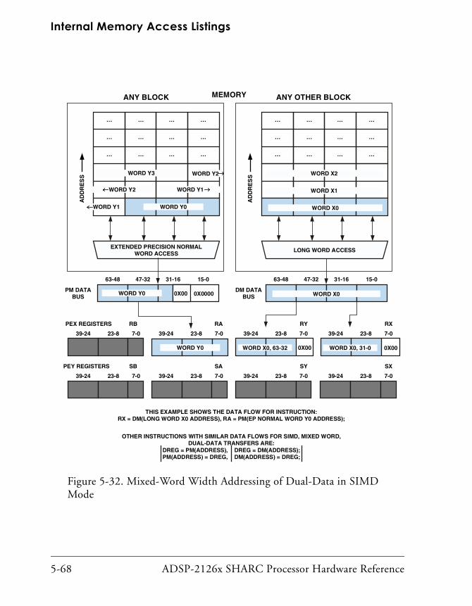
Internal Memory Access Listings
5-68 ADSP-2126x SHARC Processor Hardware Reference
Figure 5-32. Mixed-Word Width Addressing of Dual-Data in SIMD Mode
EXTENDED PRECISION NORMALWORD ACCESS
15-031-1647-3263-48
…
…
…
…
…
…
…
…
…
…
…
…
7-023-839-24
RXRYPEX REGISTERS
7-023-839-247-023-839-247-023-839-24
RARB
WORD Y0
7-023-839-24
SXSYPEY REGISTERS
7-023-839-247-023-839-247-023-839-24
SASB
PM DATABUS
OTHER INSTRUCTIONS WITH SIMILAR DATA FLOWS FOR SIMD, MIXED WORD,DUAL-DATA TRANSFERS ARE:
DREG = PM(ADDRESS), DREG = DM(ADDRESS);PM(ADDRESS) = DREG, DM(ADDRESS) = DREG;
DM DATABUS
15-031-1647-3263-48
…
…
…
…
…
…
…
…
…
…
…
…
THIS EXAMPLE SHOWS THE DATA FLOW FOR INSTRUCTION:RX = DM(LONG WORD X0 ADDRESS), RA = PM(EP NORMAL WORD Y0 ADDRESS);
LONG WORD ACCESS
0X00
WORD X0
WORD X2
WORD X0
WORD X1
WORD X0, 31-0WORD X0, 63-32 0X00
WORD Y2 WORD Y1
WORD Y0WORD Y1
WORD Y2WORD Y3
WORD Y0 0X00000X00
AD
DR
ES
S
AD
DR
ES
S
MEMORY ANY OTHER BLOCKANY BLOCK

ADSP-2126x SHARC Processor Hardware Reference 5-69
Memory
Figure 5-33. Short Word Addressing of Single-Data in Broadcast Load
WORD Y11 WORD Y10 WORD Y9 WORD Y8
WORD Y7 WORD Y6 WORD Y5 WORD Y4
WORD Y3 WORD Y2 WORD Y1
NO ACCESS
15-031-1647-3263-48
WORD Y0
…
…
…
…
…
…
…
…
…
…
…
…
PM DATABUS
MEMORY
WORD X0
OTHER INSTRUCTIONS WITH SIMILAR DATA FLOWS FOR BROADCAST, SHORT WORD, SINGLE-DATA TRANSFERS ARE:UREG = PM(SHORT WORD ADDRESS);UREG = DM(SHORT WORD ADDRESS);
DM DATABUS
WORD X11 WORD X10 WORD X9 WORD X8
WORD X7 WORD X6 WORD X5 WORD X4
WORD X3 WORD X2 WORD X1
SHORT WORD ACCESS
15-031-1647-3263-48
WORD X0
…
…
…
…
…
…
…
…
…
…
…
…
0X0000
THIS EXAMPLE SHOWS THE DATA FLOW FOR INSTRUCTION:RX = DM(SHORT WORD X0 ADDRESS);
WORD X00X0000† 0X00
7-023-839-24
RX
7-023-839-24
RA
7-023-839-24
SX
7-023-839-24
SA
WORD X00X0000† 0X00
0X0000 0X0000
AD
DR
ES
S
AD
DR
ES
S
ANY OTHER BLOCKANY BLOCK
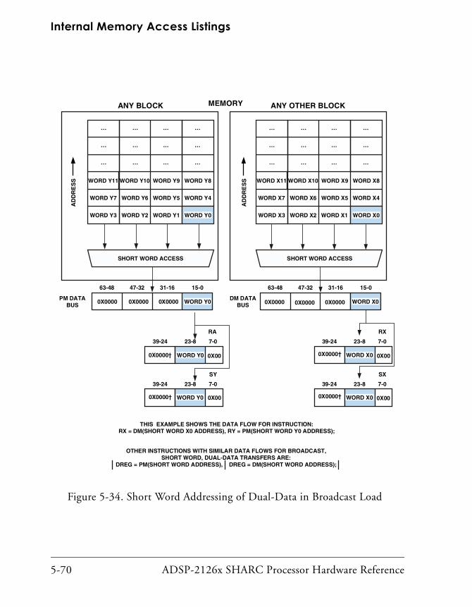
Internal Memory Access Listings
5-70 ADSP-2126x SHARC Processor Hardware Reference
Figure 5-34. Short Word Addressing of Dual-Data in Broadcast Load
WORD Y11 WORD Y10 WORD Y9 WORD Y8
WORD Y7 WORD Y6 WORD Y5 WORD Y4
WORD Y3 WORD Y2 WORD Y1
SHORT WORD ACCESS
15-031-1647-3263-48
WORD Y0
…
…
…
…
…
…
…
…
…
…
…
…
PM DATABUS
MEMORY
WORD X0
OTHER INSTRUCTIONS WITH SIMILAR DATA FLOWS FOR BROADCAST,SHORT WORD, DUAL-DATA TRANSFERS ARE:
DREG = PM(SHORT WORD ADDRESS), DREG = DM(SHORT WORD ADDRESS);
DM DATABUS
WORD X11 WORD X10 WORD X9 WORD X8
WORD X7 WORD X6 WORD X5 WORD X4
WORD X3 WORD X2 WORD X1
SHORT WORD ACCESS
15-031-1647-3263-48
WORD X0
…
…
…
…
…
…
…
…
…
…
…
…
0X0000
THIS EXAMPLE SHOWS THE DATA FLOW FOR INSTRUCTION:RX = DM(SHORT WORD X0 ADDRESS), RY = PM(SHORT WORD Y0 ADDRESS);
WORD Y00X0000
WORD X00X0000† 0X00
7-023-839-24
RX
WORD Y00X0000† 0X00
7-023-839-24
RA
7-023-839-24
SXSY
7-023-839-24
WORD X00X0000†WORD Y00X0000†
0X0000 0X0000 0X0000 0X0000
0X00 0X00
AD
DR
ES
S
AD
DR
ES
S
ANY OTHER BLOCKANY BLOCK

ADSP-2126x SHARC Processor Hardware Reference 5-71
Memory
Figure 5-35. Normal Word Addressing of Single-Data in Broadcast Load
NO ACCESS
15-031-1647-3263-48
…
…
…
…
…
…
…
…
…
…
…
…
PM DATABUS WORD X0
OTHER INSTRUCTIONS WITH SIMILAR DATA FLOWS FOR BROADCAST, NORMAL WORD, SINGLE-DATA TRANSFERS ARE:UREG = PM(NORMAL WORD ADDRESS);UREG = DM(NORMAL WORD ADDRESS);
DM DATABUS
WORD X5 WORD X4
WORD X3 WORD X2
WORD X1 WORD X0
WORD Y5 WORD Y4
WORD Y3 WORD Y2
WORD Y1 WORD Y0
NORMAL WORD ACCESS
15-031-1647-3263-48
…
…
…
…
…
…
…
…
…
…
…
…
0X0000
THE ABOVE EXAMPLE SHOWS THE DATA FLOW FOR INSTRUCTION:RX = DM(NORMAL WORD X0 ADDRESS);
WORD X0 0X00
7-023-839-24
RX
7-023-839-24
RA
7-023-839-24
SX
7-023-839-24
SA
WORD X0 0X00
0X0000
AD
DR
ES
S
AD
DR
ES
S
MEMORY ANY OTHER BLOCKANY BLOCK

Internal Memory Access Listings
5-72 ADSP-2126x SHARC Processor Hardware Reference
Figure 5-36. Normal Word Addressing of Dual-Data in Broadcast Load
NORMAL WORD ACCESS
15-031-1647-3263-48
…
…
…
…
…
…
…
…
…
…
…
…
PM DATABUS WORD X0
OTHER INSTRUCTIONS WITH SIMILAR DATA FLOWS FOR BROADCAST, NORMAL WORD, DUAL-DATA TRANSFERS ARE:DREG = PM(NORMAL WORD ADDRESS), DREG = DM(NORMAL WORD ADDRESS);
DM DATABUS
NORMAL WORD ACCESS
15-031-1647-3263-48
…
…
…
…
…
…
…
…
…
…
…
…
THIS EXAMPLE SHOWS THE DATA FLOW FOR INSTRUCTION:RX = DM(NORMAL WORD X0 ADDRESS), RA = PM(NORMAL WORD Y0 ADDRESS);
WORD Y00X0000
WORD X0 0X00
7-023-839-24
RX
WORD Y0 0X00
7-023-839-24
SY
7-023-839-24
WORD Y0 0X00
RA
7-023-839-24
SX
WORD X5 WORD X4
WORD X3 WORD X2
WORD X1 WORD X0
WORD Y5 WORD Y4
WORD Y3 WORD Y2
WORD Y1 WORD Y0
WORD X0 0X00
0X0000 0X0000 0X0000
AD
DR
ES
S
AD
DR
ES
S
MEMORY ANY OTHER BLOCKANY BLOCK

ADSP-2126x SHARC Processor Hardware Reference 5-73
Memory
Figure 5-37. Extended-Precision Normal Word Addressing of Single-Data in Broadcast Load
NO ACCESS
15-031-1647-3263-48
…
…
…
…
…
…
…
…
…
…
…
…
PM DATABUS
OTHER INSTRUCTIONS WITH SIMILAR DATA FLOWS FOR BROADCAST, EXTENDED NORMAL WORD, SINGLE-DATA TRANSFERS ARE:UREG = PM(EP NORMAL WORD ADDRESS);UREG = DM(EP NORMAL WORD ADDRESS);
DM DATABUS
15-031-1647-3263-48
…
…
…
…
…
…
…
…
…
…
…
…
THIS EXAMPLE SHOWS THE DATA FLOW FOR INSTRUCTION:RX = DM(EXTENDED PRECISION NORMAL WORD X0 ADDRESS);
7-023-839-24
RX
7-023-839-24
RA
7-023-839-24
SX
7-023-839-24
SA
WORD X0
WORD X2 WORD X1
WORD X0WORD X1
WORD X2WORD X3
WORD Y2 WORD Y1
WORD Y0WORD Y1
WORD Y2WORD Y3
EXTENDED PRECISION NORMALWORD ACCESS
0X0000
WORD X0
0X00
WORD X0
AD
DR
ES
S
AD
DR
ES
S
MEMORY ANY OTHER BLOCKANY BLOCK

Internal Memory Access Listings
5-74 ADSP-2126x SHARC Processor Hardware Reference
Figure 5-38. Extended-Precision Normal Word Addressing of Dual-Data in Broadcast Load
EXTENDED PRECISION NORMALWORD ACCESS
15-031-1647-3263-48
…
…
…
…
…
…
…
…
…
…
…
…
PM DATABUS
OTHER INSTRUCTIONS WITH SIMILAR DATA FLOWS FOR BROADCAST, EXTENDED NORMAL WORD,DUAL-DATA TRANSFERS ARE:
DREG = PM(EP NORMAL WORD ADDRESS), DREG = DM(EPNORMAL WORD ADDRESS);
DM DATABUS
15-031-1647-3263-48
…
…
…
…
…
…
…
…
…
…
…
…
THIS EXAMPLE SHOWS THE DATA FLOW FOR INSTRUCTION:RX = DM(EP NORMAL WORD X0 ADDR.), RA = PM(EP NORMAL WORD Y0 ADDR.);
WORD Y0
7-023-839-24
RXRA
WORD Y0
7-023-839-24
SY
7-023-839-24
WORD Y0
7-023-839-24
SX
WORD X0
WORD X2 WORD X1
WORD X0WORD X1
WORD X2WORD X3
WORD Y2 WORD Y1
WORD Y0WORD Y1
WORD Y2WORD Y3
EXTENDED PRECISION NORMALWORD ACCESS
0X0000
WORD X0
0X00000X00 0X00
WORD X0
AD
DR
ES
S
AD
DR
ES
S
MEMORY ANY OTHER BLOCKANY BLOCK

ADSP-2126x SHARC Processor Hardware Reference 5-75
Memory
Figure 5-39. Long Word Addressing of Single-Data in Broadcast Load
NO ACCESS
15-031-1647-3263-48
…
…
…
…
…
…
…
…
…
…
…
…
PM DATABUS
OTHER INSTRUCTIONS WITH SIMILAR DATA FLOWS FOR BROADCAST, LONG WORD, SINGLE-DATA TRANSFERS ARE:
UREG = PM(LONG WORD ADDRESS);UREG = DM(LONG WORD ADDRESS);
DM DATABUS
15-031-1647-3263-48
…
…
…
…
…
…
…
…
…
…
…
…
THIS EXAMPLE SHOWS THE DATA FLOW FOR INSTRUCTION:RX = DM(LONG WORD X0 ADDRESS);
7-023-839-24
RXRYPEX REGISTERS
7-023-839-247-023-839-247-023-839-24
RARB
7-023-839-24
SXSYPEY REGISTERS
7-023-839-247-023-839-247-023-839-24
SASB
WORD X0
WORD X2
WORD X0
WORD X1
WORD X0, 31-0
WORD Y2
WORD Y0
WORD Y1
WORD X0, 63-32
LONG WORD ACCESS
0X000X00
WORD X0, 31-0WORD X0, 63-32 0X000X00
AD
DR
ES
S
AD
DR
ES
S
MEMORY ANY OTHER BLOCKANY BLOCK

Internal Memory Access Listings
5-76 ADSP-2126x SHARC Processor Hardware Reference
Figure 5-40. Long Word Addressing of Dual-Data in Broadcast Load
LONG WORD ACCESS
15-031-1647-3263-48
…
…
…
…
…
…
…
…
…
…
…
…
PM DATABUS
OTHER INSTRUCTIONS WITH SIMILAR DATA FLOWS FOR BROADCAST, LONG WORD, DUAL-DATA TRANSFERS ARE:
DREG = PM(LONG WORD ADDRESS), DREG = DM(LONG WORD ADDRESS);
DM DATABUS
15-031-1647-3263-48
…
…
…
…
…
…
…
…
…
…
…
…
THIS EXAMPLE SHOWS THE DATA FLOW FOR INSTRUCTION:RX = DM(LONG WORD X0 ADDRESS), RA = PM(LONG WORD Y0 ADDRESS);
7-023-839-24
RXRYPEX REGISTERS
7-023-839-247-023-839-247-023-839-24
RARB
7-023-839-24
SXSYPEY REGISTERS
7-023-839-247-023-839-247-023-839-24
SASB
LONG WORD ACCESS
WORD Y0 WORD X0
WORD X2
WORD X0
WORD X1
WORD X0, 31-0
WORD Y2
WORD Y0
WORD Y1
WORD X0, 63-32WORD Y0, 31-0WORD Y0, 63-32 0X00
WORD X0, 31-0WORD X0, 63-32WORD Y0, 31-0WORD Y0, 63-32 0X00
0X00
0X00 0X00
0X00
0X00
AD
DR
ES
S
AD
DR
ES
S
0X00
MEMORY ANY OTHER BLOCKANY BLOCK

ADSP-2126x SHARC Processor Hardware Reference 6-1
6 JTAG TEST EMULATION PORT
In addition to boundary scan, the JTAG Test Emulation Port supports other functions including background telemetry channels, cycle counting with EMUCLK, user-configurable hardware support, breakpoints, and a reg-ister for viewing the revision ID.
JTAG Test Access PortThe emulator uses JTAG boundary scan logic for ADSP-2126x communi-cations and control. This JTAG logic consists of a state machine, a five pin Test Access Port (TAP), and Shift registers. The state machine and pins conform to the IEEE 1149.1 specification. The TAP pins appear in Table 6-1. A special pin (EMU) is used in the JTAG emulators from Analog Devices. This pin is not defined in the IEEE-1149.1 specification. This signal notifies the JTAG ICE that the processor has completed an operation.
Table 6-1. JTAG Test Access Port (TAP) Pins
Pin I/O Function
TCK I Test Clock: pin used to clock the TAP state machine1
1 Asynchronous with CLKIN
TMS I Test Mode Select: pin used to control the TAP state machine sequence
TDI I Test Data In: serial shift data input pin
TDO O Test Data Out: serial shift data output pin
TRST I Test Logic Reset: resets the TAP state machine

Boundary Scan
6-2 ADSP-2126x SHARC Processor Hardware Reference
A Boundary Scan Description language (BSDL) file for the ADSP-2126x is available on the Analog Devices Web site.
Refer to the IEEE 1149.1 JTAG specification for detailed information on the JTAG interface. This chapter assumes a working knowledge of the JTAG specification.
Boundary ScanA boundary scan allows a system designer to test interconnections on a printed circuit board with minimal test-specific hardware. The scan is made possible by the ability to control and monitor each input and output pin on each chip through a set of serially scannable latches. Each input and output is connected to a latch, and the latches are connected as a long Shift register so that data can be read from or written to them through a serial test access port (TAP). The ADSP-2126x contains a test access port compatible with the industry-standard IEEE 1149.1 (JTAG) specification. Only the IEEE 1149.1 features specific to the ADSP-2126x are described here. For more information, see the IEEE 1149.1 specification and the other documents listed in “References” on page 6-9.
The boundary scan allows a variety of functions to be performed on each input and output signal of the ADSP-2126x. Each input has a latch that monitors the value of the incoming signal and can also drive data into the chip in place of the incoming value. Similarly, each output has a latch that monitors the outgoing signal and can also drive the output in place of the outgoing value. For bidirectional pins, the combination of input and out-put functions is available.
Every latch associated with a pin is part of a single serial shift register path. Each latch is a master/slave type latch with the controlling clock provided externally. This clock (TCK) is asynchronous to the ADSP-2126x system clock (CLKIN).

ADSP-2126x SHARC Processor Hardware Reference 6-3
JTAG Test Emulation Port
The ADSP-2126x emulation features halt the processor at a predefined point to examine the state of the processor, execute arbitrary code, restore the original state, and continue execution.
The ADSP-2126x emulation features are a superset of the ADSP-21160 DSP emulation features. All emulation features sup-ported by previous SHARC DSPs are supported on the ADSP-2126x. The set of features on which JTAG ICE designs rely are supported in an identical fashion on ADSP-2126x. The DSP can be used with the ADSP-2106x SHARC JTAG ICE hardware.
There are several changes/extensions to the base functionality of the ADSP-2116x DSP emulation capability, which require changes in the JTAG ICE software for ADSP-2126x support. These extensions include:
• New registers for added functionality: EEMUCTL, EEMUSTAT, EEMUIN, EEMUOUT, and SHADOW_SHIFT.
• A new JTAG instruction to support these additional registers: EEMUINDATA, EEMUOUTDATA, and EEMUCTL.
• New functionality to allow the tools software to support statistical profiling.
• In addition to the IEEE boundary scan functionality, the DSP offers support for background telemetry, user-definable breakpoint interrupts, and cycle counting.
Several on-chip facilities are directly accessed through the JTAG interface. These facilities are listed in Table 6-2 on page 6-6. Other emulation facil-ities are only indirectly accessible. To indirectly access the facilities that do not appear in Table 6-2, scan the instruction which moves data of interest to/from the PX register, scan the PX data (if the instruction is a PX read), let the core execute the instruction, and then scan the PX register out (if the instruction is a PX write).

Background Telemetry Channel (BTC)
6-4 ADSP-2126x SHARC Processor Hardware Reference
The breakpoint start/end registers are mapped into the IOP register space of the ADSP-2126x. The EMUN, EMUCLK, and EMUCLK2 registers occupy the same Ureg address space as the ADSP-2106x DSP. These facilities are read-only by the ADSP-2126x core in normal operation.
Background Telemetry Channel (BTC)Programmers can read and write data to a set of memory-mapped buffers (EEMUIN and EEMUOUT) that are accessible by the emulator while the core is running. This function allows the emulator to feed new data to the DSP or get updates from the DSP in real time. A 32-bit memory-mapped I/O register called EEMUSTAT can be used to enable this functionality and check the status of the input and output data buffers. Low priority emulator interrupts are generated when the EEMUIN buffer is full or the EEMUOUT FIFO is empty so that the DSP core can handle reading/writing data from/to the buffers in an interrupt service routine (ISR). These interrupts are handled in the same way that normal interrupts are handled in the processor.
User-Definable Breakpoint InterruptsThe JTAG emulation port supports 3 interrupts:
1. EMUI (highest priority, emulator)
2. BKPI (user HW breakpoints)
3. EMULI (lowest priority, BTC)
If using the user breakpoint feature (BRKCTL register) it allows to detect legal or illegal address on all buses (DM, PM, IO). If such an exception event occurs the sequencer branches to the BKPI interrupt if enabled.

ADSP-2126x SHARC Processor Hardware Reference 6-5
JTAG Test Emulation Port
RestrictionsIf a breakpoint interrupt comes at a point when the program is coming out of an interrupt service routine (ISR) of a prior breakpoint, then in some cases the breakpoint status will not reflect that the second break-point interrupt has occurred.
If an instruction address breakpoint is placed just after a short loop, then a spurious breakpoint is generated.
Cycle Count Functionality (EMUCLK) RegisterWhen the emulator is connected to the DSP and the processor is single stepping, extra cycles are used by the emulator and this can make it seem as though the instructions are taking more cycles then the should. You can see the actual cycle time of the processor (without the emulator) by poll-ing the EMUCLK and EMUCLK2 registers. The processor cycle count can be seen while the core is in user space.
Silicon Revision IDThe ADSP-2126x contains an 8-bit revision ID (REVPID), or the Device Identification register. This register can be read by using the JTAG instruction EMUPID. The I/O address of REVPID is 0x30026.
JTAG Related RegistersInformation in this section describes public (JTAG) registers. For more information, see “Emulation Registers” on page A-45.
Instruction RegisterThe Instruction register shifts an instruction into the processor. This instruction selects the performed test and/or the access of the test data reg-

JTAG Related Registers
6-6 ADSP-2126x SHARC Processor Hardware Reference
ister. The instruction register is 5 bits long with no parity bit. A value of 10000 binary is loaded (LSB nearest TDO) into the Instruction register whenever the TAP reset state is entered.
The new JTAG instruction set, shown in Table 6-2, lists the binary code for each instruction. Bit 0 is nearest TDO and bit 4 is nearest TDI. No data registers are placed into test modes by any of the public instructions. The instructions affect the DSP as defined in the 1149.1 specification. The optional instructions RUNBIST, IDCODE, and USERCODE are not supported by the processor.
The entry under “Register” is the serial scan path, either Boundary or Bypass in this case, enabled by the instruction. Figure 6-1 shows these reg-ister paths. The 1-bit Bypass register is fully defined in the 1149.1 specification.
Table 6-2. JTAG Instruction Register Codes
43210 Register Instruction Inmode Outmode
11111 Bypass BYPASS 0 0
00000 Boundary EXTEST 0 1
10000 Boundary SAMPLE 0 0
11000 Boundary INTEST 1 1
11100 BRKSTAT EMULATION 0 0
01001 EEMUIN EMULATION 0 0
01011 EEMUOUT EMULATION 0 0
11101 EMUPID REV-id register 0 0

ADSP-2126x SHARC Processor Hardware Reference 6-7
JTAG Test Emulation Port
No special values need to be written into any register prior to the selection of any instruction. As Table 6-2 shows, certain instructions are reserved for emulator use. For more information, see Figure 6-1.
Other registers, reserved for use by Analog Devices, exist. However, this group of registers should not be accessed as they can cause damage to the part.
Figure 6-1. Serial Scan Path
0
1
2N-2
TDO
3 1
04
2
TDI 1
BOUNDARY REGISTER
BYPASS REGISTER
INSTRUCTION REGISTER
N-1
N

JTAG Related Registers
6-8 ADSP-2126x SHARC Processor Hardware Reference
Enhanced Emulation Status (EEMUSTAT) RegisterThe EEMUSTAT register acts as the breakpoint Status register for the ADSP-2126x. This register is a memory-mapped IOP register. The pro-cessor core can access this register. For I/O breakpoints, this register has two status bits, one each for the two I/O buses (IOX and IOY).
When a breakpoint is hit, a user interrupt is generated. The breakpoint status can be checked by looking at the EEMUSTAT register. When the core returns from interrupt, the breakpoint status bits will be cleared.
Boundary RegisterThe Boundary register is 163 bits long. This section defines the latch type and function of each position in the scan path. The positions are num-bered with 0 being the first bit output (closest to TDO) and 162 being the last (closest to TDI). When working with boundry scan registers keep the following points in mind:
• Scan position 0 (CLK_CFG0); this end is closest to TDO (scan in first).
• Scan position 162 (SPARE); this end is closest to TDI (scan in last).
• Output enables:
1 = Drive the associated signals during the EXTEST and INTEST instructions.
0 = Three-state the associated signals during the EXTEST and INTEST instructions
• The CLKIN signal can be sampled but not controlled (read-only). CLKIN continues to clock the ADSP-2126x no matter which instruction is enabled.

ADSP-2126x SHARC Processor Hardware Reference 6-9
JTAG Test Emulation Port
Built-In Self-Test Operation (BIST)No self-test functions are supported by the ADSP-2126x.
EMUIDLE InstructionThe EMUIDLE instruction places the DSP in the idle state and triggers an emulator interrupt. This operation uses the EMUIDLE instruction as a soft-ware breakpoint. When the EMUIDLE instruction is executed, the emulation clock counter immediately halts.
Private InstructionsTable 6-2 lists the private instructions that are reserved for emulation and memory test. The ADSP-2126x JTAG ICE emulator uses the TAP and boundary scan as a way to access the processor in the target system. The JTAG ICE emulator requires a target board connector for access to the TAP.
References• IEEE Standard 1149.1-1990. Standard Test Access Port and
Boundary-Scan Architecture.
To order a copy, contact IEEE at 1-800-678-IEEE.
• Maunder, C.M. and R. Tulloss. Test Access Ports and Boundary Scan Architectures.
IEEE Computer Society Press, 1991.
• Parker, Kenneth. The Boundary Scan Handbook.
Kluwer Academic Press, 1992.

References
6-10 ADSP-2126x SHARC Processor Hardware Reference
• Bleeker, Harry, P. van den Eijnden, and F. de Jong. Boundary-Scan Test—A Practical Approach.
Kluwer Academic Press, 1993.
• Hewlett-Packard Co. HP Boundary-Scan Tutorial and BSDL Ref-erence Guide.
(HP part# E1017-90001) 1992.
ADSP-2126x SHARC Processor Hardware Reference 7-1
7 I/O PROCESSOR
In applications that use extensive off-chip data I/O, programs may find it beneficial to use a processor resource other than the processor core to per-form data transfers. The ADSP-2126x contains an I/O processor (IOP) that supports a variety of DMA (direct memory access) operations. Each DMA operation transfers an entire block of data.
The DMA operations include the transfer types listed below and shown in Figure 7-3 on page 7-22:
• Internal memory ↔ external memory devices
• Internal memory ↔ serial port (DAI)
• Internal memory ↔ SPI I/O
• Internal memory ← IDP (DAI)
By managing DMA, the I/O processor frees the processor core, allowing it to perform other processor operations while off-chip data I/O occurs as a background task. The dual-ported internal memory allows the core and IOP to simultaneously access the same block of internal memory. This means that DMA transfers to internal memory do not impact core perfor-mance. The processor core continues to perform computations without penalty.
To further increase off-chip I/O, multiple DMAs can occur at the same time. The IOP accomplishes this by managing DMAs of processor mem-ory through the parallel, SPI, input data port (IDP) and serial ports.

General Procedure for Configuring DMA
7-2 ADSP-2126x SHARC Processor Hardware Reference
Each DMA is referred to as a channel, and each channel is configured independently.
There are 22 channels of DMA available on the ADSP-2126x processor—one channel for the SPI interface, one channel for the parallel port inter-face, 12 channels via the serial ports, and eight channels for the input data port (IDP). Another DMA feature is interrupt generation upon comple-tion of a DMA transfer or upon completion of a chain of DMAs.
General Procedure for Configuring DMATo configure the ADSP-2126x processor to use DMA, use the following general procedure.
1. Determine which DMA options you want to use:
• IOP/Core interaction method – Interrupt driven or status driven (polling)
• DMA transfer method – Chained or Non chained
• Channel priority scheme – fixed or rotating
2. Determine how you want the DMA to operate:
• Determine and set up the data’s source and/or destination addresses (INDEX)
• Set up the word COUNT (data buffer size)
• Configure the MODIFY values (step size)
3. Configure the peripheral(s):
• Serial ports (SPORTs)
• Parallel port (PP)

ADSP-2126x SHARC Processor Hardware Reference 7-3
I/O Processor
• Input data port (IDP)
4. Enable DMA by setting the applicable bits in the appropriate registers:
• parallel port – PPDEN in PPCTL
• serial port – SDEN_x (SCHEN_x for chaining) in SPCTLx
• SPI – SPIDEN (SPICHEN for chaining) in SPIDMAC
• IDP – IDP_DMA_EN in the IDP_CTL
IOP/Core Interaction OptionsThere are two methods the processor uses to monitor the progress of DMA operations—interrupts, which are the primary method, and status polling. The same program can use either method for each DMA channel. The following sections describe both methods in detail.
Interrupt-Driven I/OInterrupts on the ADSP-2126x processor are generated at the end of a DMA transfer. This happens when the count register for a particular channel decrements to zero. The interrupt vector locations for each of the channels are listed in Table 7-1. The interrupt register diagram and bit descriptions are in and “DAI Interrupt Controller Registers” on page A-164.
Programs can check the appropriate status register (for example PPCTL for the parallel port) to determine which channels are performing a DMA or chained DMA.
All DMA channels can be active or inactive. If a channel is active, a DMA is in progress on that channel. The I/O processor indicates the active sta-tus by setting the channel’s bit in the status register. The only exception to

IOP/Core Interaction Options
7-4 ADSP-2126x SHARC Processor Hardware Reference
this is the IDP_DMAx_STAT bits of the DAI_STAT register can become active even if DMA, through some IDP channel, is not intended.
The following are some other I/O processor interrupt attributes.
• When an unchained (single block) DMA process reaches comple-tion (as the count decrements to zero) on any DMA channel, the I/O processor latches that DMA channel’s interrupt. It does this by setting the DMA channel’s interrupt latch bit in the IRPTL, LIRPTL, DAI_IRPTL_H, or DAI_IRPTL_L registers.
• For chained DMA, the I/O processor generates interrupts in one of two ways: If PCI = 1, an interrupt occurs for each DMA in the chain; if PCI = 0, an interrupt occurs at the end of a complete chain. (For more information on DMA chaining, see “DMA Con-troller Operation” on page -8).
• When a DMA channel’s buffer is not being used for a DMA pro-cess, the I/O processor can generate an interrupt on single word writes or reads of the buffer. This interrupt service differs slightly for each port. For more information on single word inter-rupt-driven transfers, see “Parallel Port Control Register (PPCTL)” on page A-107, and SPCTL register in Table 9-6 on page 9-51.
During interrupt-driven DMA, programs use the interrupt mask bits in the IMASK, LIRPTL, DAI_IRPTL_PRI, DAI_IRPTL_RE, and DAI_IRPTL_FE reg-isters to selectively mask DMA channel interrupts that the I/O processor latches into the IRPTL, LIRPTL, DAI_IRPTL_H, and DAI_IRPTL_L registers.
The I/O processor only generates a DMA complete interrupt when the channel’s count register decrements to zero as a result of actual DMA transfers. Writing zero to a count register does not generate the interrupt. To stop a DMA preemptively, write a one to the count register. This causes one more word to be transferred or received and an interrupt is then generated.

ADSP-2126x SHARC Processor Hardware Reference 7-5
I/O Processor
A channel interrupt mask in the IMASK, LIRPTL, DAI_IRPTL_PRI, DAI_IRPTL_RE, and DAI_IRPTL_FE registers determines whether a latched interrupt is to be serviced or not. When an interrupt is masked, it is latched but not serviced.
By clearing a channel’s PCI bit during chained DMA, programs mask the DMA complete interrupt for a DMA process within a chained DMA sequence.
The I/O processor can also generate interrupts for I/O port operations that do not use DMA. In this case, the I/O processor generates an inter-rupt when data becomes available at the receive buffer or when the transmit buffer is not full (when there is room for the core to write to the buffer). Generating interrupts in this manner lets programs implement interrupt-driven I/O under control of the processor core. Care is needed because multiple interrupts can occur if several I/O ports transmit or receive data in the same cycle.
Table 7-1. DMA Interrupt Vector Locations
Associated Register(s) Bits Vector Address
Interrupt Name
DMA Channel
Data Buffer
IRPTL/IMASK 14 0x38 SP1I 0 RXSP1A, TXSP1A
LIRPTL 0 0x44 SP0I 2 RXSP0A, TXSP0A
IRPTL/IMASK 15 0x3C SP3I 4 RXSP3A, TXSP3A
LIRPTL 1 0x48 SP2I 6 RXSP2A, TXSP2A
IRPTL/IMASK 16 0x40 SP5I 8 RXSP5A, TXSP5A
LIRPTL 2 0x4C SP4I 10 RXSP4A, TXSP4A
IRPTL/IMASK 14 0x38 SP1I 1 RXSP1B, TXSP1B
LIRPTL 0 0x44 SP0I 3 RXSP0B, TXSP0B
IRPTL/IMASK 15 0x3C SP3I 5 RXSP3B, TXSP3B
LIRPTL 1 0x48 SP2I 7 RXSP2B, TXSP2B
IRPTL/IMASK 16 0x40 SP5I 9 RXSP5B, TXSP5B
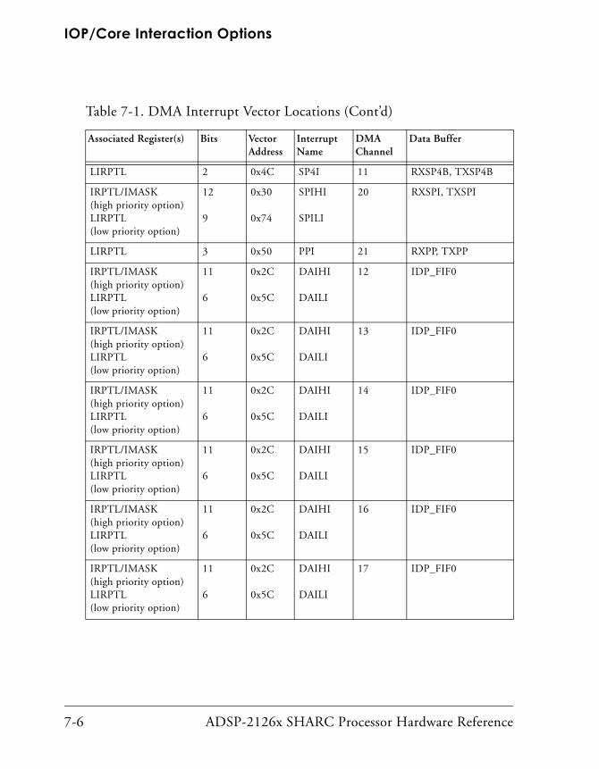
IOP/Core Interaction Options
7-6 ADSP-2126x SHARC Processor Hardware Reference
LIRPTL 2 0x4C SP4I 11 RXSP4B, TXSP4B
IRPTL/IMASK (high priority option)LIRPTL (low priority option)
12
9
0x30
0x74
SPIHI
SPILI
20 RXSPI, TXSPI
LIRPTL 3 0x50 PPI 21 RXPP, TXPP
IRPTL/IMASK (high priority option)LIRPTL (low priority option)
11
6
0x2C
0x5C
DAIHI
DAILI
12 IDP_FIF0
IRPTL/IMASK (high priority option)LIRPTL (low priority option)
11
6
0x2C
0x5C
DAIHI
DAILI
13 IDP_FIF0
IRPTL/IMASK (high priority option)LIRPTL (low priority option)
11
6
0x2C
0x5C
DAIHI
DAILI
14 IDP_FIF0
IRPTL/IMASK (high priority option)LIRPTL (low priority option)
11
6
0x2C
0x5C
DAIHI
DAILI
15 IDP_FIF0
IRPTL/IMASK (high priority option)LIRPTL (low priority option)
11
6
0x2C
0x5C
DAIHI
DAILI
16 IDP_FIF0
IRPTL/IMASK (high priority option)LIRPTL (low priority option)
11
6
0x2C
0x5C
DAIHI
DAILI
17 IDP_FIF0
Table 7-1. DMA Interrupt Vector Locations (Cont’d)
Associated Register(s) Bits Vector Address
Interrupt Name
DMA Channel
Data Buffer
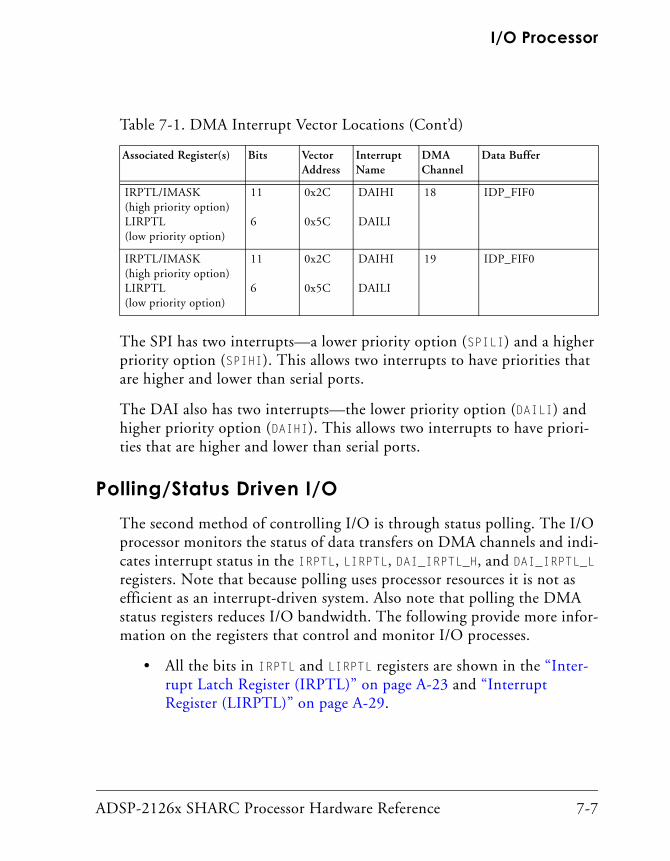
ADSP-2126x SHARC Processor Hardware Reference 7-7
I/O Processor
The SPI has two interrupts—a lower priority option (SPILI) and a higher priority option (SPIHI). This allows two interrupts to have priorities that are higher and lower than serial ports.
The DAI also has two interrupts—the lower priority option (DAILI) and higher priority option (DAIHI). This allows two interrupts to have priori-ties that are higher and lower than serial ports.
Polling/Status Driven I/OThe second method of controlling I/O is through status polling. The I/O processor monitors the status of data transfers on DMA channels and indi-cates interrupt status in the IRPTL, LIRPTL, DAI_IRPTL_H, and DAI_IRPTL_L registers. Note that because polling uses processor resources it is not as efficient as an interrupt-driven system. Also note that polling the DMA status registers reduces I/O bandwidth. The following provide more infor-mation on the registers that control and monitor I/O processes.
• All the bits in IRPTL and LIRPTL registers are shown in the “Inter-rupt Latch Register (IRPTL)” on page A-23 and “Interrupt Register (LIRPTL)” on page A-29.
IRPTL/IMASK (high priority option)LIRPTL (low priority option)
11
6
0x2C
0x5C
DAIHI
DAILI
18 IDP_FIF0
IRPTL/IMASK (high priority option)LIRPTL (low priority option)
11
6
0x2C
0x5C
DAIHI
DAILI
19 IDP_FIF0
Table 7-1. DMA Interrupt Vector Locations (Cont’d)
Associated Register(s) Bits Vector Address
Interrupt Name
DMA Channel
Data Buffer

7-8 ADSP-2126x SHARC Processor Hardware Reference
• Figure A-73 on page A-166 lists all the bits in DAI_IRPTL_H.
• Figure A-74 on page A-167 lists all the bits in DAI_IRPTL_L.
The DMA controller in the ADSP-2126x maintains the status informa-tion of the channels in each of the peripherals registers, SPMCTLxy, PPCTL, DAI_STAT, and SPIDMAC. More information on these registers can be found at the following locations.
• Bit definitions for the SPIDMAC register are illustrated in “SPI DMA Configuration (SPIDMAC) Register” on page A-101.
• Bit definitions for the SPMCTLxy register are illustrated in “SPORT Multichannel Control Registers (SPMCTLxy)” on page A-77.
• Bit definitions for the PPCTL register are illustrated in “Parallel Port Control Register (PPCTL)” on page A-107.
• Bit definitions for the DAI_STAT register are illustrated in Figure A-70 on page A-159.
There is a one cycle latency between a change in DMA channel sta-tus and the status update in the corresponding register.
If chaining is enabled on a DMA channel, programs should not use polling to determine channel status as it can provide inaccurate information. In this case, the DMA appears inactive if it is sampled while the next transfer control block (TCB) is loading.
DMA Controller OperationThere are two methods you can use to start DMA sequences: chaining and non-chaining.
Non-chained DMA. To start a new DMA sequence after the current one is finished, a program must first clear the DMA enable bit, write new

ADSP-2126x SHARC Processor Hardware Reference 7-9
I/O Processor
parameters to the index, modify, and count registers, then set the DMA enable bit to re-enable DMA.
Chained DMA. Chained DMA sequences are a set of multiple DMA operations, each autoinitializing the next in line. To start a new DMA sequence after the current one is finished, the IOP automatically loads new index, modify, and count values from an internal memory location pointed to by that channel’s chain pointer (CP) register. Using chaining, programs can set up consecutive DMA operations and each operation can have different attributes.
Chaining is only supported on the SPI and SPORT DMA chan-nels. The parallel port, and IDP port do not support chaining.
In general, a DMA sequence starts when one of the following occurs:
• Chaining is disabled, and the DMA enable bit transitions from low to high.
• Chaining is enabled, DMA is enabled, and the chain pointer regis-ter address field is written with a nonzero value. In this case, TCB chain loading of the channel parameter registers occurs first.
• Chaining is enabled, the chain pointer register address field is non-zero, and the current DMA sequence finishes. Again, TCB chain loading occurs.
A DMA sequence ends when one of the following occurs:
• The count register decrements to zero, and the CP register is zero.
• Chaining is disabled and the channel’s DMA enable bit transitions from high to low. If the DMA enable bit goes low (=0) and chain-ing is enabled, the channel enters chain insertion mode and the DMA sequence continues. For more information, see “Inserting a TCB in an Active Chain” on page 7-16.
7-10 ADSP-2126x SHARC Processor Hardware Reference
Once a program starts a DMA process, the process is influenced by two external controls—DMA channel priority and DMA chaining. For more information, see “Managing DMA Channel Priority” on page 7-18 or “Chaining DMA Processes” below.
Chaining DMA Processes
The location of the DMA parameters for the next sequence comes from the chain pointer (CP) register. In chained DMA operations, the ADSP-2126x processor automatically initializes and then begins another DMA transfer when the current DMA transfer is complete. In addition to the standard DMA parameter registers, each DMA channel (SP and SPI) also has a CP register that points to the next set of DMA parameters stored in the processor’s internal memory. In the SPI this is the CPSPI and in the SPORT it is CPSPxy. Each new set of parameters is stored in a four-word, user initialized buffer in internal memory known as a transfer control block (TCB). In TCB chain loading, the ADSP-2126x’s IOP automati-cally reads the TCB from internal memory and then loads the values into the channel parameter registers to set up the next DMA sequence.
The structure of a TCB is conceptually the same as that of a traditional linked-list. Each TCB has several data values and a pointer to the next TCB. Further, the chain pointer of a TCB may point to itself to con-stantly reiterate the same DMA.
A DMA sequence is defined as the sum of the DMA transfers for a single channel, from when the parameter registers initialize to when the count register decrements to zero. Each DMA channel has a chaining enable bit (CHEN) in the corresponding control register. This bit must be set to one to enable chaining. Chain pointer register should be cleared first before enabling chaining. When chaining is enabled, DMA transfers are initiated by writing a memory address to the CP register. This is also an easy way to start a single DMA sequence, with no subsequent chained DMAs.
The CP register can be loaded at any time during the DMA sequence. This allows a DMA channel to have chaining disabled (CP register address

ADSP-2126x SHARC Processor Hardware Reference 7-11
I/O Processor
field = 0x0000) until some event occurs that loads the CP register with a nonzero value. Writing all zeros to the address field of the chain pointer register (CP) also disables chaining.
Chained DMA operations may only occur within the same chan-nel. The processor does not support cross-channel chaining.
The parallel port and IDP port do not support DMA chaining.
The chain pointer register is 20 bits wide. The lower 19 bits are the mem-ory address field. Like other I/O processor address registers, the chain pointer register’s value is offset to match the starting address of the proces-sor’s internal memory before it is used by the I/O processor. On the ADSP-2126x, this offset value is 0x0008 0000.
Bit 19 of the chain pointer register is the Program Controlled Interrupts (PCI) bit. This bit controls whether an interrupt is latched after each DMA completes or whether the interrupt is latched after the entire DMA sequence completes. If set, the PCI bit enables a DMA channel interrupt to occur after every DMA in the chain. If cleared, an interrupt occurs at the completion of the entire DMA sequence.
Figure 7-1. TCB Chaining
CPSPxCSPxIMSPxIISPx
Address Pointerto Next TCB
Lowest Address
Highest Address
Chaining is not available on the IDP or parallel ports.An “x” denotes the DMA channel used.

IOP/Core Interaction Options
7-12 ADSP-2126x SHARC Processor Hardware Reference
The PCI bit only effects DMA channels that have chaining enabled. Also, interrupt requests enabled by the PCI bit are maskable with the IMASK register.
Because the PCI bit is not part of the memory address in the chain pointer register, programs must use care when writing and reading addresses to and from the register. To prevent errors, programs should mask out the PCI bit (bit 19) when copying the address in a chain pointer to another address register.
The DMA registers are shown in Figure 7-2.
Figure 7-2. DMA Parameter Registers
PCI BIT
31 30 29 28 27 26 25 24 23 22 21 20 19 18 17 16 15 14 13 12 11 10 9 8 7 6 5 4 3 2 1 0
CPx
31 30 29 28 27 26 25 24 23 22 21 20 19 18 17 16 15 14 13 12 11 10 9 8 7 6 5 4 3 2 1 0
EIPP
31 30 29 28 27 26 25 24 23 22 21 20 19 18 17 16 15 14 13 12 11 10 9 8 7 6 5 4 3 2 1 0
31 30 29 28 27 26 25 24 23 22 21 20 19 18 17 16 15 14 13 12 11 10 9 8 7 6 5 4 3 2 1 0
EMPP
ECPP
PROGRAM – CONTROLLED INTERRUPT BITIF THIS BIT IS SET, THE I/O PROCESSOR WILL GENERATE A
DMA INTERRUPT AFTER EVERY DMA IN THE CHAIN.
31 30 29 28 27 26 25 24 23 22 21 20 19 18 17 16 15 14 13 12 11 10 9 8 7 6 5 4 3 2 1 0
IIx
31 30 29 28 27 26 25 24 23 22 21 20 19 18 17 16 15 14 13 12 11 10 9 8 7 6 5 4 3 2 1 0
31 30 29 28 27 26 25 24 23 22 21 20 19 18 17 16 15 14 13 12 11 10 9 8 7 6 5 4 3 2 1 0
IMx
Cx

ADSP-2126x SHARC Processor Hardware Reference 7-13
I/O Processor
Transfer Control Block Chain Loading (TCB)
During TCB chain loading, the I/O processor loads the DMA channel parameter registers with values retrieved from internal memory. The address in the chain pointer register points to the highest address of the TCB (containing the index parameter). This means that if a program declares an array to hold the TCB, the CP register should not point to the first location of the array. Instead the CP register should point to array[3].
Table 7-2 shows the TCB-to-register loading sequence for the serial port and SPI port DMA channels. The I/O processor reads each word of the TCB and loads it into the corresponding register. Programs must set up the TCB in memory in the order shown in Table 7-2, placing the index parameter at the address pointed to by the CP register of the previous DMA operation of the chain. The end of the chain (no further TCBs are loaded) is indicated by a TCB with a CP value of zero.
A TCB chain load request is prioritized like all other DMA operations. The I/O processor latches a TCB loading request and holds it until the load request has the highest priority. If multiple chaining requests are present, the I/O processor services the TCB registers for the highest priority DMA channel first. A channel that is in the process of chain loading
Table 7-2. TCB Chain Loading Sequence1
1 Chaining is not available using the IDP or parallel ports.
Address2
2 An “x” denotes the DMA channel used. While the TCB is eight locations in length, SPI and serial ports only use the first four locations.
Serial Ports SPI Port
CPSPx + 0x0008 0000 IISPx IISPI
CPSPx – 1 + 0x0008 0000 IMSPx IMSPI
CPSPx – 2 + 0x0008 0000 CSPx CSPI
CPSPx – 3 + 0x0008 0000 CPSPx CPSPI

IOP/Core Interaction Options
7-14 ADSP-2126x SHARC Processor Hardware Reference
cannot be interrupted by a higher priority channel. For a list of DMA channels in priority order, see Table 7-5 on page 7-28.
Setting Up and Starting the Chain
To set up and initiate a chain of DMA operations, use these steps:
1. Clear the chain pointer register first before enabling chaining.
2. Set up all TCBs in internal memory.
3. Write to the appropriate DMA control register, setting the DMA enable bit to one and the chaining enable bit to one.
4. Write the address containing the index register value of the first TCB to the chain pointer register, which starts the chain.
The I/O processor responds by autoinitializing the first DMA parameter registers with the values from the first TCB, and then starts the first data transfer.
Setting Up and Starting Chained DMA over the SPI
Configuring and starting chained DMA transfers over the SPI port is the same as for the serial port, with one exception. Contrary to SPORT DMA chaining, (where the first DMA in the chain is configured by the first TCB), for SPI DMA chaining, the first DMA is not initialized by a TCB. Instead, the first DMA in the chain must be loaded into the SPI parameter registers (IISPI, IMSPI, CSPI), and the chain pointer register (CPSPI) points to a TCB that describes the second DMA in the sequence.
Writing an address to the CPSPI register does not begin a chained DMA sequence unless IISPI, IMSPI, and CSPI are initialized, SPI DMA is enabled, the SPI port is enabled, and SPI DMA chaining is enabled.

ADSP-2126x SHARC Processor Hardware Reference 7-15
I/O Processor
The sequence for setting up and starting a chained DMA is outlined in the following steps and can also be seen in “Chained DMA Transfers” on page 10-48.
1. Configure the TCB associated with each DMA in the chain except for the first DMA in the chain.
2. Write the first three parameters for the initial DMA to the IISPI, IMSPI, and CSPI registers directly.
3. Select a baud rate using the SPIBAUD register.
4. Select which flag to use as the SPI slave select signal in the SPIFLG register.
5. Configure and enable the SPI port with the SPICTL register.
6. Configure the DMA settings for the entire sequence, enabling DMA and DMA chaining in the SPIDMAC register.
7. Begin the DMA by writing the address of a TCB (describing the second DMA in the chain) to the CPSPI register.
8. Clear the chain pointer register before enabling chaining.
The address field of the chain pointer registers is only 19 bits wide. If a program writes a symbolic address to bit 19 of the chain pointer, there may be a conflict with the PCI bit. Programs should clear the upper bits of the address, then AND the PCI bit separately, if needed. For example,

IOP/Core Interaction Options
7-16 ADSP-2126x SHARC Processor Hardware Reference
Listing 7-1. Chain Assignment
R0=0;
dm(CPx)=R0; /* clear CPx register */
R2=(TCB1+3) & 0x7FFFF; /* init DMA control registers and
load IIx address of next TCB and
mask address */
R2=bset R2 by 19; /* set PCI bit */
dm(TCB2)=R2; /* write address to CPx location of
current TCB */
R2=(TCB2+3) & 0x7FFFF; /* load IIx address of next TCB and
mask address*/
R2=bclr R2 by 19; /* clear PCI bit */dm(TCB1)=R2; /* write address to CPx location of current TCB */dm(CPx)=R2; /* write IIx address of TCB1 to CPx
register to start chaining*/
Inserting a TCB in an Active Chain
This is supported by serial ports only. The SPI interface does not support inserting a TCB in an active chain.
It is possible to insert a single DMA operation or another DMA chain within an active DMA chain. Programs may need to perform insertion when a high priority DMA requires service and cannot wait for the cur-rent chain to finish.
When DMA on a channel is disabled and chaining on the channel is enabled, the DMA channel is in chain insertion mode. This mode lets a program insert a new DMA or DMA chain within the current chain with-out effecting the current DMA transfer. Use the following sequence to

ADSP-2126x SHARC Processor Hardware Reference 7-17
I/O Processor
insert a DMA subchain for the serial port 0A channel while another chain is active:
1. Enter chain insertion mode by setting SCHEN_A = 1 and SDEN_A = 0 in the channel’s DMA control register, SPCTL0. The DMA inter-rupt indicates when the current DMA sequence has completed.
2. Copy the address currently held in the chain pointer register to the chain pointer position of the last TCB in the chain that is being inserted.
3. Write the start address of the first TCB of the new chain into the chain pointer register.
4. Resume chained DMA mode by setting SCHEN_A = 1 and SDEN_A = 1.
Chain insertion mode operates the same as non-chained DMA mode. When the current DMA transfer ends, an interrupt request occurs and no TCBs are loaded. This interrupt request is independent of the PCI bit state.
Chain insertion should not be set up as an initial mode of opera-tion. This mode should only be used to insert one or more TCBs into an active DMA chaining sequence.
Setting Up DMA Channel Allocation and PrioritiesThe ADSP-2126x processor has 22 DMA channels including 12 channels accessible via the serial ports, one SPI channel, one parallel port channel, and eight input data port channels. Each channel has a set of parameter registers which are used to set up DMA transfers. Table 7-3 shows the DMA channel allocation and parameter register assignments for the ADSP-2126x processor. DMA channel 0 has the highest priority and DMA channel 21 has the lowest priority.

IOP/Core Interaction Options
7-18 ADSP-2126x SHARC Processor Hardware Reference
Managing DMA Channel Priority
The default channel priority is: DMA channel 0 as highest priority and DMA channel 22 as lowest priority. Table 7-5 on page 7-28 lists the DMA channels in priority order. When a channel becomes the highest priority requester, the I/O processor services the channel’s request. In the next clock cycle, the I/O processor starts the DMA transfer.
The I/O data (IOD) bus is 32 bits wide and is the only path that the IOP uses to transfer data between internal memory and the peripherals. When there are two or more peripherals with active DMAs in progress, they may all require data to be moved to or from memory in the same cycle. For example, the parallel port may fill its RXPP buffer just as a SPORT shifts a word into its RXn buffer. To determine which word is transferred first, the DMA channels for each of the processor’s I/O ports negotiate channel pri-ority with the I/O processor using an internal DMA request/grant handshake.
Each I/O port has one or more DMA channels, and each channel has a single request and a single grant. When a particular channel needs to read or write data to internal memory, the channel asserts an internal DMA request. The I/O processor prioritizes the request with all other valid DMA requests. When a channel becomes the highest priority requester, the I/O processor asserts the channel’s internal DMA grant. In the next clock cycle, the DMA transfer starts. Figure 7-4 on page 7-27 shows the paths for internal DMA requests within the I/O processor.
If a DMA channel is disabled (PPDEN, SPIDEN, SDEN, or IDP_DMA_EN bits =0), the I/O processor does not issue internal DMA grants to that channel (whether or not the channel has data to transfer).
The default DMA channel priority is fixed prioritization by DMA channel group (serial ports, parallel port, IDP, or SPI port). Table 7-5 on page 7-28 lists the DMA channels in descending order of priority.
For information on programming serial port priority modes, see Table 9-7 on page 9-65.

ADSP-2126x SHARC Processor Hardware Reference 7-19
I/O Processor
The I/O processor determines which DMA channel has the highest prior-ity internal DMA request during every cycle between each data transfer.
Processor core accesses of I/O processor registers and TCB chain loading (both of which occur after the IOD transfer) are subject to the same prior-itization scheme as the DMA channels. Applying this scheme uniformly prevents I/O bus contention, because these accesses are also performed over the internal I/O bus. For more information, see “Chaining DMA Processes” on page 7-10.
DMA Bus Arbitration
DMA channel arbitration is the method that the IOP uses to determine how groups rotate priority with other channels. This feature is enabled by setting the DCPR bit in the IOP’s SYSCTL register.
DMA-capable peripherals execute DMA data transfers to and from inter-nal memory over the IOD bus. When more than one of these peripherals requests access to the IOD bus in a clock cycle, the bus arbiter, which is attached to the IOD bus, determines which master should have access to the bus and grants the bus to that master.
IOP channel arbitration can be set to use either a fixed (SYSCTL[7] = 0) or rotating (SYSCTL[7] = 1) algorithm.
In the fixed priority scheme, the lower indexed peripheral has the highest priority.
In the rotating priority scheme, the default priorities at reset are the same as that of the fixed priority. However, the peripheral priority is deter-mined by group, not individually. Peripheral groups are shown in Table 7-3.
Initially, Group A has the highest priority and Group F the lowest. As one group completes its DMA operation, it is assigned the lowest priority (moves to the back of the line) and the next group is given the highest priority.

IOP/Core Interaction Options
7-20 ADSP-2126x SHARC Processor Hardware Reference
When none of the peripherals request bus access, the highest priority peripheral, for example, peripheral#0, is granted the bus. However, this does not change the currently assigned priorities to various peripherals.
Within a peripheral group the priority is highest for the higher indexed peripheral (see Table 7-3). For example in SP01 (group A), SP1 has the highest priority.
Table 7-3. DMA Channel Allocation and Parameter Register Assignments
DMA Channel Number
Data Buffer Group IOP Address of Data Buffers
Description
0 (highest pri-ority)
RXSP1A, TXSP1A A 0xC65, 0xC64 Serial Port 1A Data
1 RXSP1B, TXSP1B A 0xC67, 0xC66 Serial Port 1B Data
2 RXSP0A, TXSP0A A 0xC61, 0xC60 Serial Port 0A Data
3 RXSP0B, TXSP0B A 0xC63, 0xC62 Serial Port 0 B Data
4 RXSP3A, TXSP3A B 0x465, 0x464 Serial Port 3A Data
5 RXSP3B, TXSP3B B 0x467, 0x466 Serial Port 3B Data
6 RXSP2A, TXSP2A B 0x461, 0x460 Serial Port 2A Data
7 RXSP2B, TXSP2B B 0x463, 0x462 Serial Port 2B Data
8 RXSP5A, TXSP5A C 0x865 or 0x864 Serial Port 5A Data
9 RXSP5B, TXSP5B C 0x867 or 0x866 Serial Port 5B Data
10 RXSP4A, TXSP4A C 0x861 or 0x860 Serial Port 4A Data
11 RXSP4B, TXSP4B C 0x863 or 0x862 Serial Port 4B Data
12 IDP_FIF0 D 0x24D0 DAI IDP Channel 0
13 IDP_FIF0 D 0x24D0 DAI IDP Channel 1
14 IDP_FIF0 D 0x24D0 DAI IDP Channel 2
15 IDP_FIF0 D 0x24D0 DAI IDP Channel 3

ADSP-2126x SHARC Processor Hardware Reference 7-21
I/O Processor
Setting Up DMA Parameter RegistersOnce you have determined and configured the DMA options, you can configure the DMA parameter registers. The parameter registers control the source and destination of the data, the size of the data buffer, and the step size used. These topics are described in detail in the following sections.
DMA Transfer DirectionDMA transfers between internal memory and external memory devices use the processor’s parallel port. For these types of transfers, a program pro-vides the DMA controller with the internal memory buffer size, address, and address modifier, as well as the external memory buffer size, address and address modifier and the direction of transfer. After setup, the DMA transfers begin when the program enables the channel and continues until the I/O processor transfers the entire buffer to processor memory. Table 7-4 on page 7-25 shows the parameter registers for each DMA channel.
16 IDP_FIF0 D 0x24D0 DAI IPD Channel 4
17 IDP_FIF0 D 0x24D0 DAI IDP Channel 5
18 IDP_FIF0 D 0x24D0 DAI IDP Channel 6
19 IDP_FIF0 D 0x24D0 DAI IDP Channel 7
20 RXSPI, TXSPI E 0x1004, 0x1003 SPI Data
21 (lowest priority)
RXPP, TXPP F 0x1809, 0x1808 Parallel Port Data
Table 7-3. DMA Channel Allocation and Parameter Register Assignments (Cont’d)
DMA Channel Number
Data Buffer Group IOP Address of Data Buffers
Description

Setting Up DMA Parameter Registers
7-22 ADSP-2126x SHARC Processor Hardware Reference
Similarly, DMA transfers between internal memory and serial, IDP or SPI ports have DMA parameters. When the I/O processor performs DMA between internal memory and one of these ports, the program sets up the parameters, and the I/O uses the port instead of the external bus.
The direction (receive or transmit) of the I/O port determines the direc-tion of data transfer. When the port receives data, the I/O processor automatically transfers the data to internal memory. When the port needs to transmit a word, the I/O processor automatically fetches the data from internal memory. Figure 7-4 on page 7-27 shows more detail on DMA channel data paths. Figure 7-3 shows the processor’s I/O processor, related ports, and buses.
Figure 7-3. I/O Processor Block Diagram
IDP FIFO(8 DEEP)
PARALLELPORT FIFOS
(2 DEEP)
SPORTFIFOS
(2 DEEP)
SPI PORTFIFOS
(1 DEEP) SIG
NA
LR
OU
TIN
GU
NIT
(DA
I)
IOD BUS32-BIT
DMA BUS ARBITRATION / IOP MUX
DMD, PMD BUSES(64-BIT, TO CORE)
I/O PROCESSORREGISTERS
(IOP DOMAIN)
I/O PROCESSORREGISTERS
(CORE DOMAIN)
SPIDMAFIFO
(4 DEEP)
I/O PROCESSOR

ADSP-2126x SHARC Processor Hardware Reference 7-23
I/O Processor
Data Buffer RegistersThe data buffer registers in Figure 7-3 on page 7-22 shows the data buffer registers for each port. These registers include:
• Serial Port Receive Buffer (RXSPx). These receive buffers for the serial ports have two position FIFOs for receiving data when con-nected to another serial device.
• Serial Port Transmit Buffer (TXSPx). These transmit buffers for the serial ports have two position FIFOs for transmitting data when connected to another serial device.
• SPI Receive Buffer (RXSPI). This receive buffer for the SPI port has a single position buffer for receiving data when connected to another serial device.
• SPI Transmit Buffer (TXSPI). This transmit buffer for the SPI port has a single position buffer for transmitting data when connected to another serial device.
• Parallel Port Transmit Buffer (TXPP). This transmit buffer for the parallel port has two-position FIFOs for transmitting data when connected to another device.
• Parallel Port Receive Buffer (RXPP). This receive buffer for the par-allel port has two position FIFOs for receiving data when connected to another parallel device.
• Input Data Port Buffers (IDP_FIFO). This receive buffer for the input data port has eight position buffers for receiving data when connected to another device.

Setting Up DMA Parameter Registers
7-24 ADSP-2126x SHARC Processor Hardware Reference
Port, Buffer, and DMA Control RegistersThe Port, Buffer, and DMA Control Registers in Figure 7-3 shows the control registers for the ports and DMA channels. These registers include:
• Parallel Port Control register (PPCTL). This register enables the parallel port system, DMA, and external data width. It also config-ures wait states, bus hold cycles and identifies the status of the parallel port FIFO, internal, and external interfaces.
• Input Data Port Control register (IDP_CTL). This is the control register for input data ports.
• Serial Port Control registers (SPCTLx, SPMCTLxy). These control registers select the receive or transmit format, monitor FIFO status, enable chaining, and start DMA for each serial port.
• SPI Port Control register (SPICTL). This control register config-ures and enables the SPI interface, selects the device as master or slave, and determines the data transfer and word size. The SPIDMAC register also controls SPI DMA and FIFO status.
Table 7-4 shows the parameter registers for each DMA channel. These registers function similarly to data address generator registers and include:
• Internal Index registers (IISPx, IISPI, IIPP, IDP_DMA_Ix). Index registers provide an internal memory address, acting as a pointer to the next internal memory DMA read or write location.
• Internal Modify registers (IMSPx, IMPP, IMSPI, IDP_DMA_Mx). Mod-ify registers provide the signed increment by which the DMA controller post-modifies the corresponding internal memory index register after the DMA read or write.
• Count registers (CSPx, ICPP, CSPI, IDP_DMA_Cx). Count registers indicate the number of words remaining to be transferred to or from internal memory on the corresponding DMA channel.

ADSP-2126x SHARC Processor Hardware Reference 7-25
I/O Processor
• Chain Pointer registers (CPSPx, CPSPI). Chain pointer registers hold the starting address of the TCB (parameter register values) for the next DMA operation on the corresponding channel. These reg-isters also control whether the I/O processor generates an interrupt when the current DMA process ends.
• External Index register (EIPP). Index register provides an external memory address, acting as a pointer to the next external memory DMA read or write location.
• External Modify registers (EMPPx). Modify registers provide the increment by which the DMA controller post-modifies the corre-sponding external memory index register after the DMA read or write.
• External Count registers (ECPPx). External count registers indicate the number of words remaining to be transferred to or from exter-nal memory on the corresponding DMA channel.
Table 7-4. ADSP-2126x Processor DMA Channel Parameter Registers
Register Function Width Description
IIy Internal Index Register 19 bits Address of buffer in internalmemory
IMxy Internal Modify Register 16 bits1
1 IDP_DMA_Mx are 6 bits wide only.
Stride for internal buffer
Cxy Internal Count Register 16 bits Length of internal buffer
CPxy Chain Pointer Register 20 bits Chain pointer for DMA chaining
EIPP External Index Register 19 bits Address of buffer in externalmemory
EMPP External Modify Register 2 bits Stride for external buffer
ECPP External Count Register 16 bits Length of external buffer
Setting Up DMA Parameter Registers
7-26 ADSP-2126x SHARC Processor Hardware Reference
AddressingFigure 7-4 shows a block diagram of the I/O processor’s address generator (DMA controller). Table 7-4 lists the parameter registers for each DMA channel. The parameter registers are uninitialized following a processor reset.
The I/O processor generates addresses for DMA channels much the same way that the Data Address Generators (DAGs) generate addresses for data memory accesses. Each channel has a set of parameter registers including an index register and modify register that the I/O processor uses to address a data buffer in internal memory. The index register must be initialized with a starting address for the data buffer. As part of the DMA operation, the I/O processor outputs the address in the index register onto the pro-cessor’s I/O address bus and applies the address to internal memory during each DMA cycle—a clock cycle in which a DMA transfer is taking place.
All addresses in the index registers are offset by a value matching the pro-cessor’s first internal normal word addressed RAM location, before the I/O processor uses the addresses. For the ADSP-2126x processor, this off-set value is 0x0008 0000.
DMA addresses must always be normal word (32-bit) memory, and inter-nal memory data transfer sizes are 32 bits. External data transfer sizes may be 16 or 8 bits. The I/O processor can transfer short word data (16-bit) using the packing capability of the serial port and SPI port DMA channels.
After transferring each data word to or from internal memory, the I/O processor adds the modify value to the index register to generate the address for the next DMA transfer and writes the modified index value to the index register. The modify value in the modify register is a signed inte-ger, which allows both increment and decrement modifies. The modify value can have any positive or negative integer value.

ADSP-2126x SHARC Processor Hardware Reference 7-27
I/O Processor
Figure 7-4. DMA Address Generator
LOCAL BUS
CXCOUNT
CPXCHAIN POINTER
MUX
– 1
WORKING REGISTER
+
LOCAL BUS
IMXMODIFIER
INTERNALMEMORYADDRESS
IIXINDEX (ADDRESS)
+/-POST-MODIFY
DMA ADDRESS GENERATOR (INTERNAL ADDRESSES)
DMA WORD COUNTER
LOCAL BUS
EMPPEXT. MODIFIER
ECPPEXT. COUNT
– 1
EXTERNALMEMORYADDRESS
POST-MODIFY
EIPPEXT. INDEX (ADDRESS)
++
DMA ADDRESS GENERATOR (EXTERNAL ADDRESSES)

Setting Up DMA Parameter Registers
7-28 ADSP-2126x SHARC Processor Hardware Reference
If the I/O processor modifies the index register past the maximum 19-bit value to indicate an address out of internal memory, the index wraps around to zero. With the offset for the ADSP-2126x processor, the wraparound address is 0x0008 0000.
If a program loads the count register with zero, the I/O processor does not disable DMA transfers on that channel. The I/O proces-sor interprets the zero as a request for 216 transfers. This count occurs because the I/O processor starts the first transfer before test-ing the count value. The only way to disable a DMA channel is to clear its DMA enable bit.
If a DMA channel is disabled, the I/O processor does not service requests for that channel, whether or not the channel has data to transfer.
The processor’s 22 DMA channels are numbered as shown in Table 7-5. This table also shows the control, parameter, and data buffer registers that correspond to each channel.
In SP01, SP1 has a higher priority. Similarly, for SP23 and SP45, the odd numbered SPs have a higher priority (SP3, SP5).
Table 7-5. DMA Channel Registers: Controls, Parameters and Buffers
DMA Channel Number
Control Registers
Parameter Registers Buffer Registers Description
0 SPCTL1 IISP1A, IMSP1A, CSP1A, CPSP1A
RXSP1A, TXSP1A Serial Port 1A Data
1 SPCTL1 IISP1B, IMSP1B, CSP1B, CPSP1B
RXSP1B, TXSP1B Serial Port 1B Data
2 SPCTL0 IISP0A, IMSP0A, CSP0A, CPSP0A
RXSP0A, TXSP0A Serial Port 0A Data
3 SPCTL0 IISP0B, IMSP0B, CSP0B, CPSP0B
RXSP0B, TXSP0B Serial Port 0B Data

ADSP-2126x SHARC Processor Hardware Reference 7-29
I/O Processor
4 SPCTL3 IISP3A, IMSP3A, CSP3A, CPSP3A
RXSP3A, TXSP3A Serial Port 3A Data
5 SPCTL3 IISP3B, IMSP3B, CSP3B, CPSP3B
RXSP3B, TXSP3B Serial Port 3B Data
6 SPCTL2 IISP2A, IMSP2A, CSP2A, CPSP2A
RXSP2A, TXSP2A Serial Port 2A Data
7 SPCTL2 IISP2B, IMSP2B, CSP2B, CPSP2B
RXSP2B, TXSP2B Serial Port 2B Data
8 SPCTL5 IISP5A, IMSP5A, CSP5A, CPSP5A
RXSP5A, TXSP5A Serial Port 5A Data
9 SPCTL5 IISP5B, IMSP5B, CSP5B, CPSP5B
RXSP5B, TXSP5B Serial Port 5B Data
10 SPCTL4 IISP4A, IMSP4A, CSP4A, CPSP4A
RXSP4A, TXSP4A Serial Port 4A Data
11 SPCTL4 IISP4B, IMSP4B, CSP4B, CPSP4B
RXSP4B, TXSP4B Serial Port 4B Data
12 IDP_CTL IDP_DMA_I0, IDP_DMA_M0, IDP_DMA_C0
IDP_FIFO DAI IDP Channel 0
13 IDP_CTL IDP_DMA_I1, IDP_DMA_M1, IDP_DMA_C1
IDP_FIFO DAI IDP Channel 1
14 IDP_CTL IDP_DMA_I2, IDP_DMA_M2, IDP_DMA_C2
IDP_FIFO DAI IDP Channel 2
15 IDP_CTL IDP_DMA_I3, IDP_DMA_M3, IDP_DMA_C3
IDP_FIFO DAI IDP Channel 3
Table 7-5. DMA Channel Registers: Controls, Parameters and Buffers (Cont’d)
DMA Channel Number
Control Registers
Parameter Registers Buffer Registers Description

Setting Up DMA
7-30 ADSP-2126x SHARC Processor Hardware Reference
All of the I/O processor’s registers are memory-mapped, ranging from address 0x0000 0000 to 0x0003 FFFF. For more information on these registers, see “Core Registers” on page A-1.
Setting Up DMABecause the I/O processor registers are memory-mapped, the processor has access to program DMA operations. A processor sets up a DMA channel by writing the transfer’s parameters to the DMA parameter registers. After the index, modify, and count registers (among others) are loaded with a starting source or destination address, an address modifier, and a word count, the processor is ready to start the DMA.
16 IDP_CTL IDP_DMA_I4, IDP_DMA_M4, IDP_DMA_C4
IDP_FIFO DAI IPD Channel 4
17 IDP_CTL IDP_DMA_I5, IDP_DMA_M5, IDP_DMA_C5
IDP_FIFO DAI IDP Channel 5
18 IDP_CTL IDP_DMA_I6, IDP_DMA_M6, IDP_DMA_C6
IDP_FIFO DAI IDP Channel 6
19 IDP_CTL IDP_DMA_I7, IDP_DMA_M7, IDP_DMA_C7
IDP_FIFO DAI IDP Channel 7
20 SPICTL IISPI, IMSPI, CSPI, CPSPI
RXSPI, TXSPI SPI Data
21 PPCTL EIPP, EMPP, ECPP, IIPP, IMPP, ICPP
RXPP, TXPP Parallel Port Data
Table 7-5. DMA Channel Registers: Controls, Parameters and Buffers (Cont’d)
DMA Channel Number
Control Registers
Parameter Registers Buffer Registers Description

ADSP-2126x SHARC Processor Hardware Reference 7-31
I/O Processor
The SPI port, parallel port, serial ports and input data ports each have a DMA enable bit (SPIDEN, PPDEN, SDEN or IDP_DMA_EN) in their channel control register. Setting this bit for a DMA channel with configured DMA parameters starts the DMA on that channel.
If the parameters configure the channel to receive, the I/O processor trans-fers data words received at the buffer to the destination in internal memory. If the parameters configure the channel to transmit, the I/O pro-cessor transfers a word automatically from the source memory to the channel’s buffer register. These transfers continue until the I/O processor transfers the selected number of words as determined by the count param-eter. DMA through the IDP ports occurs in internal memory only.

Setting Up DMA
7-32 ADSP-2126x SHARC Processor Hardware Reference

ADSP-2126x SHARC Processor Hardware Reference 8-1
8 PARALLEL PORT
The ADSP-2126x processor has a parallel port that allows bidirectional transfers between it and external parallel devices. Using the parallel port bus and control lines, the processor can interface to 8-bit or 16-bit wide external memory devices. The parallel port provides a DMA interface between internal and external memory and has the ability to support core driven data transfer modes. Regardless of whether 8-bit or 16-bit external memory devices are used, the internal data word size is always 32 bits (normal word addressing), and the parallel port employs packing to place the data appropriately.
This chapter describes the parallel port operation, registers, interrupt function, and transfer protocol. Figure 8-1 shows a block diagram of the parallel port.
The processor provides two data packing modes, 8/32 and 16/32. For reads, data packing involves shifting multiple successive 8- or 16-bit ele-ments from the parallel port to the ADSP-2126x’s Receive register to form each 32-bit word, transferring multiple successive 8-bit or 16-bit ele-ments. For writes, packing involves shifting each 32-bit word out into 8- or 16-bit elements that are placed into the memory device.

8-2 ADSP-2126x SHARC Processor Hardware Reference
Figure 8-1. Parallel Port Block Diagram
PARALLEL PORTCONTROLLER
ALE
INTERNALMEMORY
EXTERNAL ADDRESS
RXPP
RD
WR
AD[15-0]
PPSI MUX
PPSOTXPP
DMAPARALLEL
PORT
IMPP
ICPP
EIPP
EMPP
ECPP
PPCTL
IIPP
COREACCESS
TRANSMIT REGISTER
RECEIVE REGISTER

ADSP-2126x SHARC Processor Hardware Reference 8-3
Parallel Port
Parallel Port PinsThis section describes the pins that the parallel port uses for its operation. For a complete list of pin descriptions and package pinouts, see the prod-uct specific data sheet for your device.
• Address/Data (AD15–0) pins. The ADSP-2126x processor pro-vides time multiplexed address/data pins that are used for providing both address and data information. The state of the address/data pins is determined by the 8- or 16-bit operating mode and the state of the ALE, RD, and WR pins.
• Read strobe (RD) pin. This output pin is asserted low to indicate a read operation. Data is latched into the processor using the rising edge of this signal.
• Write strobe (WR) pin. This output pin is asserted low to indicate a write operation. The rising edge of this signal can be used by mem-ory devices to latch the data from the processor.
• Address Latch Enable (ALE) pin. The address latch enable pin is used to strobe an external latch connected to the address/data pins (AD15–0). The external latch holds the most significant bits (MSBs) of the external memory address. An ALE cycle is inserted for the first access after the parallel port is enabled and anytime the upper 16 bits of the address change from a previous cycle.
In 8-bit mode, a maximum of 24 bits of external address are facilitated through latching the upper 16 bits, EA23–8, from AD15–0 into the external latch during the ALE phase of the cycle. The remaining 8 bits of address EA7–0 are provided through AD15–8 during the second half of the cycle when the RD or WR signal is asserted.
In 16-bit mode, a maximum of 16 bits of external address are facilitated through latching the upper 16 bits of AD15–0 from AD15–0 into the exter-nal latch during the ALE phase of the cycle. The AD15–0 represent the

Parallel Port Pins
8-4 ADSP-2126x SHARC Processor Hardware Reference
external 16 bits of data during the second half of the cycle when the RD or WR signal is asserted.
The ALE pin is active high by default, but can be set active low via the PPA-LEPL bit (bit 13) in the Parallel Port Control (PPCTL) register.
Since ALE polarity is active high by default, systems using parallel port boot mode must use address latching hardware that can pro-cess this active high signal.
Alternate Pin FunctionsThe following sections describe how to make the parallel port pins func-tion as flag pins and how to make the parallel data acquisition port pins function as address pins. For additional information on pin multiplexing, see “Pin Multiplexing” on page 15-2.
Parallel Ports as FLAG Pins
Setting (= 1) bit 20 in the SYSCTL register, (PPFLGS) causes the 16 address pins to function as FLAG0-FLAG15. To use the parallel port for data access, this bit should be cleared (= 0). For more information, see “System Design” on page 15-1.
The ADSP-2126x supports up to 16 general-purpose FLAG pins. These FLAG signals are multiplexed with other signals, and may be used in several different ways. If the parallel port is disabled, then the 16 address and data pins become FLAG0–FLAG15. If the parallel port is in use, then these same 16 FLAG signals can be routed through the SRU, to 16 DAI pins. Finally, FLAG0–FLAG3 are available on four separate pins. These pins are shared with IRQ0–2 and TIMEXP.
Configuring the parallel port pins to function as FLAG0–15 also causes these four dedicated pins to change to their alternate role, IRQ0–2 and TIMEXP.

ADSP-2126x SHARC Processor Hardware Reference 8-5
Parallel Port
Parallel Data Acquisition Port as Address Pins
PDAP use of AD[15:0] pins. When bit 26 of the IDP_PP_CTL register is set, the Parallel Data Acquisition Port (PDAP) reads from the parallel port’s AD0–15 pins. When this bit is cleared, the PDAP reads data using DAI pins DAIP20–5. To use the parallel port, this bit must be cleared (= 0). For more information, see “Parallel Data Acquisition Port (PDAP)” on page 11-6.
Parallel Port OperationThis section describes how the parallel port transfers data. The SYSCTL and PPCTL registers control the parallel port operating mode.
Basic Parallel Port External TransactionA parallel port external transaction consists of a combination of an ALE cycle and a data cycle, which is either a read or write cycle. The following section describes parallel port operation as it relates to processor timing. Refer to the data sheet for your processor for detailed timing specifications.
An ALE cycle is an address latch cycle. In this cycle the RD and WR signals are inactive and ALE is strobed. The upper 16 bits of the address are driven onto the AD15–0 lines, and shortly thereafter the ALE pin is strobed, with AD15–0 remaining valid slightly after de-assertion to ensure a sufficient hold time for the external latch. The ALE pin always remains high for 2 x CCLK, irrespective of the data cycle duration values that are set in the PPCTL register. The parallel port runs at 1/3 the CCLK rate, and so the ALE cycle is 3 x CCLK. An ALE cycle is inserted whenever the upper 16 bits of address differs from a previous access, as well as after the parallel port is enabled.

Parallel Port Operation
8-6 ADSP-2126x SHARC Processor Hardware Reference
In a read cycle, the WR and ALE signals are inactive and RD is strobed. If the upper 16 bits of the external address have changed, this cycle is always pre-ceded by an ALE cycle. In 8-bit mode, the lower 8 bits of the address, EA7–0, are driven on the AD15–8 pins, and data is sampled from the AD7–0 pins on the rising edge of RD. In 16-bit mode, address bits are not driven in the read cycle, the external address is provided entirely by the external latch, and data is sampled from the AD15–0 pins at the rising edge of RD. Read cycles can be lengthened by configuring the parallel port data cycle dura-tion bits in the PPCTL register.
In a write cycle, RD and ALE are inactive and WR is strobed. If the upper 16 bits of the external address have changed, this cycle is always preceded by an ALE cycle. In 8-bit mode, the lower 8 bits of the address are driven on the AD15–8 pins and data is driven on the AD7–0 pins. In 16-bit mode, address bits are not driven in the write cycle, the external address is pro-vided entirely by the external latch, 16-bit data is driven onto the AD15-0 pins, and data is written to the external device on the rising edge of the WR signal. Address and data are driven before the falling edge of WR and deas-serted after the rising edge to ensure enough setup and hold time with respect to the WR signal. Write cycles can be lengthened by configuring the parallel port data cycle duration bits in the PPCTL register.
Reading From an External Device or MemoryThe parallel port has a two stage data FIFO for receiving data (RXPP). In the first stage, a 32-bit register (PPSI) provides an interface to the external data pins and packs the 8- or 16-bit data into 32 bits. Once the 32-bit data is received in PPSI, the data is transferred into the second 32-bit reg-ister (RXPP). Once the receive FIFO is full, the chip cannot initiate any more external data transfers. The RXPP register acts as the interface to the core or I/O processor (for DMA).
The PPTRAN bit must be zero in order to be read.
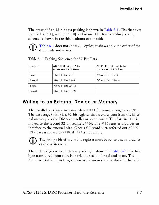
ADSP-2126x SHARC Processor Hardware Reference 8-7
Parallel Port
The order of 8 to 32-bit data packing is shown in Table 8-1. The first byte received is [7:0], second [15:8] and so on. The 16- to 32-bit packing scheme is shown in the third column of the table.
Table 8-1 does not show ALE cycles; it shows only the order of the data reads and writes.
Writing to an External Device or MemoryThe parallel port has a two stage data FIFO for transmitting data (TXPP). The first stage (TXPP) is a 32-bit register that receives data from the inter-nal memory via the DMA controller or a core write. The data in TXPP is moved to the second 32-bit register, PPSO. The PPSO register provides an interface to the external pins. Once a full word is transferred out of PPSO, TXPP data is moved to PPSO, if TXPP is not empty.
The PPTRAN bit of the PPCTL register must be set to one in order to enable writes to it.
The order of 32- to 8-bit data unpacking is shown in Table 8-2. The first byte transferred from PPSO is [7:0], the second [15:8] and so on. The 32-bit to 16-bit unpacking scheme is shown in column three of the table.
Table 8-1. Packing Sequence for 32-Bit Data
Transfer AD7–0, 8-bit to 32-bit (8-bit bus, LSW first)
AD15–0, 16-bit to 32-bit (16-bit bus, LSW first)
First Word 1; bits 7–0 Word 1; bits 15–0
Second Word 1; bits 15–8 Word 1; bits 31–16
Third Word 1; bits 23–16
Fourth Word 1; bits 31–24

8-8 ADSP-2126x SHARC Processor Hardware Reference
Table 8-2 does not show ALE cycles; it shows only the order of the data reads and writes.
Parallel port DMAs can only be performed to 32-bit (normal word) internal memory.
Transfer ProtocolThe external interface follows the standard asynchronous SRAM access protocol. The programmable Data Cycle Duration (PPDUR) and optional Bus Hold Cycle (BHC) addition at the end of each data cycle are provided to interface with memories having different access time requirements. The data cycle duration is programmed via the PPDUR bit in the PPCTL register. The hold cycle at the end of the data cycle is programmed via the PPBHC bit in the PPCTL register.
Disabling the parallel port (PPEN bit is cleared) flushes both parallel port FIFOs, RXPP, and TXPP.
For standard asynchronous SRAM there are two transfer modes—8-bit and 16-bit mode. In 8-bit mode, the address range is 0x0 to 0xFFFFFF which is 16M bytes (4M 32-bit words). In 16-bit mode, the address range is 0x0 to 0xFFFF which is a 128K bytes (32K 32-bit words). Although programs can initiate reads or writes on one and two byte boundaries, the parallel port always transfers 4 bytes (two 16-bit or four 8-bit words).
Table 8-2. Unpacking Sequence for 32-Bit Data
Transfer AD7–0, 32-bit to 8-bit (8-bit bus, LSW first)
AD15–0, 32-bit to 16-bit (16-bit bus, LSW first)
First Word 1; bits 7–0 Word 1; bits 15–0
Second Word 1; bits 15–8 Word 1; bits 31–16
Third Word 1; bits 23–16
Fourth Word 1; bits 31–24

ADSP-2126x SHARC Processor Hardware Reference 8-9
Parallel Port
8-Bit Mode
An ALE cycle always precedes the first transfer of data after the parallel port is enabled. During ALE cycles for 8-bit mode, the upper 16 bits of the external address (EA23–8) are driven on the 16-bit parallel port bus (pins AD15–0). In data cycles (reads and writes), the processor drives the lower 8 bits of address EA7–0 on AD15–8. The 8 bits of external data, ED7–0, that are provided by AD7–0, are sampled by the RD/WR signal respectively. The processor continues to receive and or send data with the same ALE cycle until the upper 16 bits of external address differ from the previous access. For consecutive accesses (EMPP = 1), this occurs once every 256 cycles. Figure 8-2 shows the connection diagram for the 8-bit mode.
Eight-bit mode enables a larger external address range.
16-Bit Mode
In 16-bit mode, the external address range is EA15–0 (64K addressable 16-bit words). For a nonzero stride value (EMPP = 0), the transfer of data
Figure 8-2. External Transfer—8-bit Mode
LATCH
ADSP-2126x
AD[7-0]
ALE
RD
WR
AD[15-8] ADDR[7-0]
DATA[7-0]
D[7-0]
ALE
D[15-8] Q[15-0] ADDR[23-8]
RD
WR
SRAM
DATA[7-0]
180V
68V
CE
CESRAMCE
FLASHCE
8
8FLASH

8-10 ADSP-2126x SHARC Processor Hardware Reference
occurs in two cycles. In cycle one, the processor performs an ALE cycle, driving the 16 bits of external address, EA15–0, onto the 16-bit parallel port bus (pins AD15–0), allowing the external latch to hold this address. In the second cycle, the processor either drives or receives the 16 bits of external data (ED15–0) through the 16-bit parallel port bus (pins AD15–0). This pattern repeats until the transfer completes.
However, a special case occurs when the external address modifier is zero, (EMPP = 0). In this case, the external address is latched only once, using the ALE cycle before the first data transfer. After the address has been latched externally, the processor continues receiving and sending 16-bit data on AD15–0 until the transfer completes. This mode can be used with external FIFOs and high speed A/D and D/A converters and offers the maximum throughput available on the parallel port (132 Mbyte/sec).
Figure 8-3 shows the connection diagram in 16-bit mode.
Figure 8-3. External Transfer—16-bit Mode
LATCH
ADSP-2126x
ALE
RD
WR
AD[15-0] DATA[17-0]
ALE
Q[15-0] ADDR[23-8]
RD
WR
SRAM
DATA[7-0]
180V
68V
CE
CESRAMCE
FLASHCE
16
16
16
FLASH

ADSP-2126x SHARC Processor Hardware Reference 8-11
Parallel Port
Comparison of 16-Bit and 8-Bit SRAM ModesWhen considering whether to employ the 16- or 8-bit mode in a particu-lar design, a few key points should be considered.
• The 8-bit mode provides a 24-bit address, and therefore can access 16M bytes of external memory. In contrast, the 16-bit mode can only address 64K x 16 bit words, which is equivalent to 128K bytes. Therefore, the 8-bit mode provides 128 times the storage capacity of the 16-bit mode.
• For sequential accesses, the 8-bit mode requires only one ALE cycle per 256 bytes. With minimum wait states selected, this represents a worst case overhead of:(1 ALE cycle)/(256 accesses + 1 ALE) x 100% = 0.39% overhead for ALE cycles. In contrast, the 16-bit mode requires one ALE cycle per external sequential access. Regardless of length (N), this represents a worst case overhead of:(N ALE cycles)/(N accesses + N ALE cycles) x 100% = 50% overhead for ALE cycles. However, the 16-bit mode delivers two bytes per cycle. Therefore, the total data transfer speed for sequential accesses is nearly identical for both 8-bit and 16-bit modes.
The question that arises at this point is: If the total transfer rates are the same for both 8-bit and 16-bit modes, and the 8-bit mode can also address 128 times as much external memory, why would a system use the 16-bit mode?
• Sometimes an external device is only capable of interfacing to a 16-bit bus.
• When the DMA external modifier is set to zero, the address does not change after the first cycle, therefore an ALE cycle is only inserted on the first cycle. In this case, the 16-bit port can run
Parallel Port Interrupt
8-12 ADSP-2126x SHARC Processor Hardware Reference
twice as fast as the 8-bit port, as the overhead for ALE cycles is zero. This is convenient when interfacing to high speed 16-bit FIFO-based devices, including A/D and D/A converters.
• In situations where a majority of address accesses are non-sequen-tial and cross 256 byte boundaries, the overhead of the ALE cycles in the 8-bit mode approaches 20%1. In this particular situation, the 16-bit memory can provide a 40% speed advantage over the 8-bit mode.
Parallel Port InterruptThe parallel port has one interrupt signal, PPI, (bit 3 in the LIRPTL regis-ter). When DMA is enabled, the maskable interrupt PPI occurs when the DMA block transfer has completed (when the DMA Internal Word Count register ICPP decrements to zero). When DMA is disabled, the maskable interrupt is latched in every cycle the receive buffer is not empty or the transmit buffer is not full.
The parallel port receive (RXPP) and transmit (TXPP) buffers are memory mapped IOP registers. The PPI bit is located at vector address 0x50. The latch (PPI), mask (PPIMSK) and mask pointer (PPIMSKP) bits associated with the parallel port interrupt are all located in the LIRPTL register.
Parallel Port ThroughputAs described in “Parallel Port Operation”, each 32-bit word transferred through the parallel port takes a specific period of time to complete. This throughput depends on a number of factors, namely parallel port speed (1/3 core instruction rate), memory width (8 bits or 16 bits), and memory
1 This can be realized by recalling that four bytes must be packed/unpacked into a single 32-bit word. For example when a 32-bit word is written/read, there is a single ALE cycle inserted per four consecu-tive addresses. This results in: (N/4 ALE cycles)/(N accesses + N/4 ALE cycles) x 100% = 20%.

ADSP-2126x SHARC Processor Hardware Reference 8-13
Parallel Port
access constraints (occurrence of ALE cycles at page boundaries, duration of data cycles, and/or addition of hold time cycles).
The maximum parallel port speed is 1/3 of the core. The relationship between core clock and parallel port speed is static. For a 200 MHz core clock, the parallel port runs at 66 MHz. Since there is no parallel port clock signal, it is easiest to think of parallel port throughput in terms of core clock cycles.
As described in “Parallel Port Operation” on page 8-5, parallel port accesses require both ALE cycles to latch the external address and addi-tional data cycles to transmit or receive data. Therefore, the throughput on the parallel port is determined by the duration and number of these cycles per word. The duration of each type of cycle is shown below and the frequency is determined by the external memory width.
There is one case where the frequency is also determined by the external address modifier register (EMPP).
• ALE cycles are fixed at 3 core cycles (CCLK) and are not affected by the PPDUR or BHC bit settings. In this case, the ALE is high for 2 core clock cycles. Address for ALE is set up a half core clock cycle before ALE goes HIGH (active) and remains on bus a half cycle after ALE goes LOW (inactive). Therefore, the total ALE cycles on the bus are 1/2 + 2 + 1/2 = 3 core clock cycles. Please refer to the data sheet for more precise timing characteristics.
• Data cycle duration is programmable with a range of 3 to 32 CCLK cycles. They may range from 4 to 33 cycles if the BHC bit is set (=1).
The following sections show examples of transfers that demonstrate the expected throughput for a given set of parameters. Each word transfer sequence is made up of a number of data cycles and potentially one addi-tional ALE cycle.

Parallel Port Throughput
8-14 ADSP-2126x SHARC Processor Hardware Reference
8-Bit AccessIn 8-bit mode, the first data-access (whether a read or a write) always con-sists of one ALE cycle followed by four data cycles. As long as the upper 16 bits of address do not change, each subsequent transfer consists of four data cycles. The ALE cycle is inserted only when the parallel port address crosses an 8-bit boundry page, in other words, after every 256 bytes that are transferred.
For example, if PPDUR3, BHC = 0, and the processor is in 8-bit mode. The first byte on a new page takes six core cycles (three for the ALE cycle and three for the data cycle), and the next sequential 255 bytes consume three core cycles each.
Therefore, the average data rate for a 256 byte page is: (3 CCLK x 255 + 6 CCLK x 1) / 256 = 3.01 core clock cycles per byte.
For a 200 MHz core, this results in:
(200M CCLK /sec) x (1 byte/3.008 CCLK) = 66.4M bytes/sec
16-Bit AccessIn 16-bit mode, every word transfer consists of two ALE cycles and two data cycles. Therefore, for every 32-bit word transferred, at least six CCLK cycles are needed to transfer the data plus an additional six CCLK cycles for the two ALE cycles, for a total of 12 CCLK cycles per 32-bit transfer (four bytes). For a 200 MHz core clock, this results in a maximum sustained data rate device of:
200 MHz /12 = 16.67 Million 32-bit words/sec = 66.6M Bytes/sec
There is a specific case which allows this maximum rate to be exceeded. If the external address modifier (EMPP) is set to a stride of zero, then only one

ADSP-2126x SHARC Processor Hardware Reference 8-15
Parallel Port
ALE cycle is needed at the very start of the transfer. Subsequent words, essentially written to the same address, do not require any ALE cycles, and every parallel port cycle may be a 16-bit data cycle. In this case, the throughput is nearly doubled (except for the very first ALE cycle) to over 132M bytes per second. This mode is particularly useful for interfacing to FPGA’s or other memory-mapped peripherals such as DAC/ADC converters.
ConclusionFor sequential accesses, the average data rates are nearly identical in 8- and 16-bit modes. For help deciding between the two modes, please refer to “Comparison of 16-Bit and 8-Bit SRAM Modes” on page 8-11.
Parallel Port RegistersThe ADSP-2126x’s parallel port contains several user-accessible registers. The Parallel Port Control Register, PPCTL, contains control and status bits and is described below. Two additional registers, RXPP and TXPP, are used for buffering receive and transmit data during DMA operations and can be accessed by the core. Finally, the following registers are used for every parallel port access (both core-driven and DMA-driven).
• “Parallel Port DMA Start External Index Address Register (EIPP)” on page A-110
• “Parallel Port DMA External Modifier Address Register (EMPP)” on page A-111

Parallel Port Registers
8-16 ADSP-2126x SHARC Processor Hardware Reference
For DMA transfers only, the following registers must also be initialized:
• “Parallel Port DMA Internal Word Count Register (ICPP)” on page A-110
• “Parallel Port DMA Start Internal Index Address Register (IIPP)” on page A-110
• “Parallel Port DMA Internal Modifier Address Register (IMPP)” on page A-110
• “Parallel Port DMA External Word Count Register (ECPP)” on page A-111
Additional information on Parallel Port registers can be found in “Parallel Port Registers” on page A-105.
Parallel Port DMA RegistersThe following registers require initialization only when performing DMA-driven accesses.
• DMA Start Internal Index Address (IIPP) register
This 19-bit register contains the offset from the DMA starting address of 32-bit internal memory.
• DMA Internal Modifier Address (IMPP) register
This 16-bit register contains the internal memory DMA address modifier.
• DMA Internal Word Count (ICPP) register
This 16-bit register contains the number of words in internal mem-ory to be transferred via DMA.
• Parallel Port DMA External Word Count (ECPP) register

ADSP-2126x SHARC Processor Hardware Reference 8-17
Parallel Port
This 24-bit register contains the number of words in external memory to be transferred via DMA.
Parallel Port External Setup RegistersThe following registers must be initialized for both core-driven and DMA-driven transfers.
• Parallel Port DMA External Index Address (EIPP) register
This 24-bit register contains the external memory byte address used for core-driven and DMA driven transfers.
• Parallel Port External Address Modifier (EMPP) register
This 2-bit register contains the external memory DMA address modifier. It supports only +1, 0, –1. After each data cycle, the EIPP register is modified by this value.
Using the Parallel PortThere are a number of considerations to make when interfacing to parallel external devices. This section describes the different the ways that the par-allel port can be used to access external devices. Considerations for choosing between an 8-bit and a 16-bit wide interface are discussed in “Comparison of 16-Bit and 8-Bit SRAM Modes” on page 8-11.
External parallel devices can be accessed in two ways, either using DMA-driven transfers or core-driven transfers. DMA transfers are per-formed in the background by the I/O Processor and are generally used to move blocks of data. To perform DMA transfers, the address, word-count, and address-modifier are specified for both the source and destination buf-fers (one internal, one external). Once initiated, (by setting PPEN = 1 and PPDEN = 1), the IOP performs the specified transfer in the background without further core interaction. The main advantage of DMA transfers

Using the Parallel Port
8-18 ADSP-2126x SHARC Processor Hardware Reference
over core driven transfers is that the core can continue executing code while sequential data is imported/exported in the background.
Unlike the external port on previous SHARC processors, the ADSP-2126x core cannot directly access the external parallel bus. Instead, the core ini-tializes two registers to indicate the external address and address-modifier and then accesses data through intermediate registers. Then, when the core accesses either the PPTX or PPRX registers, the parallel port writes/fetches data to/from the specified external address. The details of this functionality and the four main techniques to manage each transfer are detailed below. In general, core-driven transfers are most advantageous when performing single-word accesses and/or accesses to non-sequential addresses.
DMA TransfersTo use the parallel port for DMA programs, start by setting up values in the DMA parameter registers. The program then writes to the PPCTL regis-ter to enable PPDEN with all of the necessary settings like cycle duration value, transfer direction, and so on. While a parallel port DMA is active, the DMA parameter registers are not writable. Furthermore, only the PPEN and DMAEN bits (in the PPCTL register) can be changed. If any other bit is changed, the parallel port will malfunction. It is recommended that both the PPDEN and PPEN bits be set and reset together to ensure proper DMA operation.
To see an example program that sets up a parallel port DMA, see Listing 8-1 on page 8-23.
Core Driven TransfersCore-driven transfers can be managed using four techniques. The transfers can 1) use interrupts, 2) poll status bits in the PPCTL register, 3) predict when each access will complete by calculating the data and ALE cycle dura-tions, or 4) rely on the fact that the core stalls on certain accesses to PPRX

ADSP-2126x SHARC Processor Hardware Reference 8-19
Parallel Port
and PPTX. For all four of these methods, the core uses the same basic steps to initiate the transfer. However, each method uses a different technique to complete it. The following steps provide the basic procedure for setting up and initiating a data transfer using the core.
1. Write the external byte address to the EIPP register and the external address modifier to the EMPP register.
Before initializing or modifying any of the parallel port parameter registers such as EIPP and EMPP, the parallel port must first be dis-abled (bit 0, PPEN, of the PPCTL register must be cleared). Only when PPEN=0, can those registers be modified and the port then re-enabled. This sequence is most often used to perform non-sequential, external transfers, such as when accessing taps in a delay line.
For core-driven transfers, the ECPP, IIPP, IMPP, and ICPP are not used. Although these registers are automatically updated by the parallel port (the ECPP register decrements for example), they may be left uninitialized without consequence.
2. Initialize the PPCTL register with the appropriate settings.
These include the parallel port data-cycle duration (PPDUR) and whether the transfer is a receive or transmit operation (PPTRAN). For core-driven transfers, be sure to clear the DMA enable bit, PPDEN. In this same write to PPCTL, the port may also be enabled by setting bit 0, PPEN, to 1.
When enabling the parallel port (setting PPEN = 1), the external bus activ-ity varies, depending on the direction of data transfer (receive or transmit). For transmit operations (PPTRAN = 1), the parallel port does not perform any external accesses until valid data is written to the TXPP register by the core.
For read operations (PPTRAN = 0), two core clock cycles after PPEN is set (=1), the parallel port immediately fetches two 32-bit data words from the

Using the Parallel Port
8-20 ADSP-2126x SHARC Processor Hardware Reference
external byte address indicated by EIPP. Subsequently, additional data is fetched only when the core reads (empties) RXPP.
The following are guidelines that programs must follow when the proces-sor core accesses parallel port registers.
• While a DMA transfer is active, the core may only write the PPEN and PPDEN bits of PPCTL. Accessing any of the DMA parameter reg-isters or other bits in PPCTL during an active transfer will cause the parallel port to malfunction.
• Core reads of the FIFO register during a DMA operation are allowed but do not affect the status of the FIFO.
If PPEN is cleared while a transfer is underway (whether core or DMA-driven), the current external bus cycle (ALE cycle or data cycle) will complete but no further external bus cycles occur. Dis-abling the parallel port clears the data in the RXPP and TXPP registers.
• Core reads and writes to the TXPP and RXPP registers update the sta-tus of the FIFO when DMA is not active. This happens even when the parallel port is disabled.
• The PPCTL register has a two-cycle effect-latency. This means that if programs write to this register in cycle N, the new settings will not be in effect until cycle N + 2. Avoid sampling PPBS until at least 2 cycles after the PPEN bit in PPCTL is set.
• For core-driven transfers over the parallel port, the IIPP, IMPP, ICPP, and ECPP registers are not used. Only the EIPP and EMPP regis-ters need to be initialized before accessing the TXPP or RXPP buffers.
Known Duration Accesses
Of these methods, known duration accesses are the most efficient because they allow the core to execute code while the transfer to/from the RXPP or

ADSP-2126x SHARC Processor Hardware Reference 8-21
Parallel Port
TXPP occurs on the external bus. For example, after the core reads the PPTX register, it will take some number N core-cycles for the PP to shift out that data to the memory. During that time, the core can go on doing other tasks. After N core-cycles have passed, the parallel port may be disabled and the external address register updated for another access.
To determine the duration for each access, the designer simply add's the number of data-cycles and the duration of each (measured in CCLK cycles) along with the number of ALE cycles (which are fixed at 3 CCLK cycles). This duration is deterministic, and is based on two settings in the PPCTL register—parallel port data-cycle duration (PPDUR) and Bus Hold Cycle Enable (PPBHC).
Please refer to “Parallel Port Operation” for further explanation of the par-allel port bus cycles, but in summary, programs can use the following values:
• each ALE cycle is fixed at 3 CCLK cycles, regardless of the PPDUR or PPBHC settings.
• each Data cycle is the setting in the PPDUR register (+1 if PPBHC =1)
For example, in 8-bit mode, a single-word transfer is comprised of 1 ALE cycle and 4 Data cycles. If PPDUR3 is used (the fastest case) and PPBHC = 0, this transfer completes in:
(1 ALE-cycle x 3 CCLK) + (4 data-cycles x 3 CCLK) = 15 core cycles per 32-bit word.
This means that 15-instructions after data is written to TXPP or read from RXPP, the parallel port has finished writing/fetching that data externally, and the parallel port may be disabled. This case is shown in Listing 8-3 on page 8-27.

Using the Parallel Port
8-22 ADSP-2126x SHARC Processor Hardware Reference
Status Driven Transfers (Polling)
The second method that the core may use to manage parallel port transfers involves the status bits in PPCTL register, specifically the Parallel Port Bus Status (PPBS) bit. This bit reflects the status of the external address pins AD0-AD15 and is used to determine when it is safe to disable and modify the parallel port. The PPBS bit is set to 1 at the start of each transfer, and is cleared once the entire 32-bit word has been transmitted/received.
Core-Stall Driven Transfers
The final method of managing parallel port transfers simply relies on the fact that the core will stall execution when reading from an empty RX buf-fer and when writing to a full TX buffer. This technique can only be used for accesses to sequential addresses in external memory. For sequential external addresses, the parallel port does not need to be disabled after each word in order to manually update the EIPP register. Instead, the external address that is automatically incremented by the modifier (EMPP) register on each access is used.
Interrupt Driven Accesses
With interrupt-driven accesses, parallel port interrupts are generated on a word-by-word basis, rather than on a block transfer basis, as is the case when DMA is enabled. In this non-DMA mode, the interrupt indicates to the core that it is now safe to read a word from the RXPP buffer or to write a word to the TXPP buffer (depending on the value of the PPTRAN bit).
To facilitate this, the PPI (latch) bit of the LIRPTL register is set to one in every core cycle where the TXPP buffer is not full or, in receive mode, in every core cycle in which the RXPP buffer has valid data. When fast 16-bit wide parallel devices are accessed, there may be as few as 10 core cycles between each transfer. Because of this, interrupt-driven transfers are usu-ally the least efficient method to use for core-driven accesses. Interrupt driven transfers are most valuable when parallel port data-cycle durations are very long (allowing the core may do some work between accesses).

ADSP-2126x SHARC Processor Hardware Reference 8-23
Parallel Port
Generally, interrupts are the best choice for DMA-driven parallel port transfers rather than core-driven transfers.
Parallel Port Programming ExamplesThis section provides two programming examples written for the ADSP-21262 processor. The first, Listing 8-1, uses the parallel port to transfer a buffer to 16-bit external memory using DMA. The second example Listing 8-2, uses the parallel port to transfer a buffer to 8-bit external memory using status driven core writes. The last example, shows a calculated duration example of core driven parallel port access.
Listing 8-1. Parallel Port DMA Buffer Transfer
/* Register Definitions */
#define PPCTL 0x1800
#define EIPP 0x1810
#define EMPP 0x1811
#define ECPP 0x1812
#define IIPP 0x1818
#define IMPP 0x1819
#define ICPP 0x181a
/* Register Bit Definitions */
#define PPEN 0x00000001
#define PPDUR20 0x00000026
#define PPBHC 0x00000040
#define PP16 0x00000080
#define PPDEN 0x00000100
#define PPTRAN 0x00000200
#define PPBS 0x00020000
/* Source Buffer */

Parallel Port Programming Examples
8-24 ADSP-2126x SHARC Processor Hardware Reference
.section/dm seg_dmda;
.var source[8] = 0x11111111,
0x22222222,
0x33333333,
0x44444444,
0x55555555,
0x66666666,
0x77777777,
0x88888888;
.global _main;
.section/pm seg_pmco;
_main:
ustat3 = dm(PPCTL); /*disable parallel port*/
bit clr ustat3 PPEN|PPDEN;
dm(PPCTL) = ustat3;
/* initiate parallel port DMA registers*/
r0 = source; dm(IIPP) = r0;
r0 = 1; dm(IMPP) = r0;
r0 = LENGTH(source); dm(ICPP) = r0;
r0 = 1; dm(EMPP) = r0;
r0 = 0x1000000; dm(EIPP) = r0;
/* For 16-bit external memory, the External count is
double the internal count */
r0 = LENGTH(source) * 2; dm(ECPP) = r0;
ustat3 = PP16| /* for a 16-bit external memory */
PPTRAN| /* transmit (write) */
PPBHC| /* implement a bus hold cycle*/
PPDUR20; /* make pp data cycles last for a duration
of 20 cclk cycles */
dm(PPCTL) = ustat3;

ADSP-2126x SHARC Processor Hardware Reference 8-25
Parallel Port
/* initiate PP DMA*/
/*Enable Parallel Port and PP DMA in same cycle*/
ustat4 = dm(PPCTL);
bit set ustat4 PPDEN|PPEN;
dm(PPCTL) = ustat4;
_main.end: jump(pc,0);
Listing 8-2. Parallel Port Status Driven Core Transfer
/* Register Definitions */
#define PPCTL 0x1800
#define TXPP 0x1808
#define RXPP 0x1809
#define EIPP 0x1810
#define EMPP 0x1811
#define ECPP 0x1812
/* Register Bit Definitions */
#define PPEN 0x00000001
#define PPDUR20 0x00000026
#define PPBHC 0x00000040
#define PPTRAN 0x00000200
#define PPBS 0x00020000
/* Source Buffer */
.section/dm seg_dmda;
.var source[8] = 0x11111111,
0x22222222,
0x33333333,
0x44444444,
0x55555555,
0x66666666,

Parallel Port Programming Examples
8-26 ADSP-2126x SHARC Processor Hardware Reference
0x77777777,
0x88888888;
/* Main code section */
.global _main;
.section/pm seg_pmco;
_main:
i4 = source;
m4 = 1;
/* setup ppdma registers for core use */
r0 = 1; dm(EMPP) = r0;
r0 = 0x1000000; dm(EIPP) = r0;
/* For 8-bit external memory, the External count is
four times the internal count */
r0 = LENGTH(source) * 4; dm(ECPP) = r0;
ustat3 = PPEN| /* enable port */
PPTRAN| /* transmit (write) */
PPBHC| /* implement a bus hold cycle*/
PPDUR20; /* make pp data cycles last for a */
/* duration of 20 cclk cycles */
dm(PPCTL) = ustat3;
/* loop to write 10 words into TXPP */
lcntr = 10, do core_writes until lce;
write:
r0 = dm(i4,m4);
core_writes: dm(TXPP) = r0;
/* poll to ensure parallel port has completed the transfer */
waiting: ustat4 = dm(PPCTL);
bit tst ustat4 PPBS;
if tf jump waiting;
_main.end: jump(pc,0);

ADSP-2126x SHARC Processor Hardware Reference 8-27
Parallel Port
Listing 8-3. Calculated Duration Core Driven Access
_main: /* Setup once========================================= */
ustat3 = PPDUR3 | PPTRAN | PPEN; /* ustat3 enables PP */
ustat4 = PPDUR3 | PPTRAN; /* ustat4 disables PP */
dm(PPCTL) = ustat4; /* initialize but disable PP */
/* NOTE: Internal DMA registers AND the EXTERNAL COUNT can be
left uninitialized for Core-driven transfers (External count
determined by bus width: 16bit = count of 2, 8-bit = count of 4,
since internal width always = 32-bits.) */
r0=1; dm(EMPP)=r0; /* don't move external ptr */
/* initialize external address and sample-to-write */
r1=EZKIT_SRAM_BASE_ADDR; /* initialize R1 w/ first
ext. byte address */
r2=0x33221100; /* and R2 w/ first data to be
written /* /* =============================================== */
/* for testing */ do (write_loop.end - 1) until forever;
/* ===Instructions required for each 32-bit word written===*/
/* (18 instructions per sample = 4 cycles overhead + 14 cycles
work) /* /* R1 holds external byte address to be written */
/* R2 holds data to be written */
write_loop:

Parallel Port Programming Examples
8-28 ADSP-2126x SHARC Processor Hardware Reference
dm(EIPP) = r1;
dm(PPCTL)= ustat3; /* enable PP */
dm(TXPP) = r2; /* <-- write to PP FIFO */
/* -----14 core cycles (minimum) available while each word is
being transmitted. Writting to PPCTL has a 2 cycle
effect-latency, so the result of writing this register in the
14th cycle doesn't take effect until the 16th cycle - which is
one cycle after the cycle completes----- */
/* (NOTE: Modifying PP parameters before 14 cycles have passed
will cause the access to fail - Using more than 14 cycles is
fine. */
nop;nop;
nop;nop;
nop;nop;
nop;nop;
nop;nop;
nop;
/* update addr and data for next loop iteration: r0 = 4;
r1 = R1 + r0; /* next ext. destination address += 4
r2 = r2 + 1; /* next data to write /* /*-----------------------------------------------------------*/
dm(PPCTL)=ustat4; /* <-- 14 cycles later, it's safe to
disable/alter PP because each access takes
15 CCLK cycles, and writing PPCTL has a
2-cycle effect-latency. */
/* NOTE: PPEN must be cleared before modifying EIPP /* ========================================================

ADSP-2126x SHARC Processor Hardware Reference 9-1
9 SERIAL PORTS
The ADSP-2126x processors have up to six independent, synchronous serial ports (SPORTs) that provide an I/O interface to a wide variety of peripheral devices. Each serial port has its own set of control registers and data buffers. With a range of clock and frame synchronization options, the SPORTs allow a variety of serial communication protocols and provide a glueless hardware interface to many industry-standard data converters and codecs.
The number of serial ports varies depending on the specific proces-sor model you are using. This chapter was written using six serial ports for examples. Programs need to be written accordingly.
Serial ports can operate at one-quarter the full clock rate of the processor, at a maximum clock rate of n/4M bit/s, where n equals the processor core-clock frequency (CCLK). If channels A and B are active, each SPORT has 100M bit/s maximum throughput. Bidirectional (transmit or receive) functions provide greater flexibility for serial communications. Serial port data can be automatically transferred to and from on-chip memory using DMA block transfers. In addition to standard synchronous serial mode, each serial port offers a Time Division Multiplexed (TDM) multichannel
mode, Left-justified Sample Pair mode, and I2S mode.
Serial ports offer the following features and capabilities:
• Two bidirectional channels (A and B) per serial port, configurable as either transmitters or receivers. Each serial port can also be con-figured as two receivers or two transmitters, permitting two unidirectional streams into or out of the same serial port. This

9-2 ADSP-2126x SHARC Processor Hardware Reference
bidirectional functionality provides greater flexibility for serial communications. Further, two SPORTs can be combined to enable full-duplex, dual-stream communications.
• All serial data signals have programmable receive and transmit functions and thus have one transmit and one receive data buffer register (double-buffer) and a bidirectional shift register associated with each serial data signal. Double-buffering provides additional time to service the SPORT.
• μ-law and A-law compression/decompression hardware compand-ing on transmitted and received words.
• An internally-generated serial clock and frame sync provide signals in a wide range of frequencies. Alternately, the SPORT can accept clock and frame sync input from an external source, as described in Figure 9-8 on page 9-63.
• Interrupt-driven, single word transfers to and from on-chip mem-ory controlled by the processor core, described in “Single Word Transfers” on page 9-73.
• DMA transfers to and from on-chip memory. Each SPORT can automatically receive or transmit an entire block of data.
• Chained DMA operations for multiple data blocks, see “Chaining DMA Processes” on page 7-10.
• Four operation modes: DSP Standard Serial, Left-justified Sample Pair, I2S, and multichannel. In standard DSP serial, Left-justified Sample Pair, and I2S modes, when both A and B channels are used, they transmit or receive data simultaneously, sending or receiving bit 0 on the same edge of the serial clock, bit 1 on the next edge of the serial clock, and so on. In multichannel mode, SPORT1, 3 or 5 can receive A and B channel data, and SPORT0, 2 or 4 transmits A and B channel data selectively from up to 128 channels of a TDM serial bitstream. This mode is useful for H.100/H.110 and other

ADSP-2126x SHARC Processor Hardware Reference 9-3
Serial Ports
telephony interfaces. In multichannel mode, SPORT0 and SPORT1 work as a pair, SPORT2 and SPORT3 work as a pair, and SPORT4 and SPORT5 work as a pair. See “SPORT Opera-tion Modes” on page 9-9.
When programming the serial port channel (A or B) as a transmit-ter, only the corresponding transmit buffers TXSPxA and TXSPxB become active, while the receive buffers (RXSPxA and RXSPxB) remain inactive. Similarly, when SPORT channels A and B are pro-grammed to receive, only the corresponding RXSPxA and RXSPxB buffers are activated.
SPORTs are forced into pairs when in multichannel mode. For more information, see “Multichannel Operation” on page 9-24.
• The serial ports are configurable for transferring data words between 3 and 32 bits in length, either most significant bit (MSB) first or least significant bit (LSB) first. Words must be between 8 and 32 bits in length for I2S and Left-justified Sample Pair mode. Refer to “Data Word Formats” on page 9-39 and the individual SPORTs operation mode sections for additional information.
• 128-channel TDM is supported in multichannel mode operation, described in “Multichannel Operation” on page 9-24.
Receive comparison and 2-dimensional DMA are not supported in the ADSP-2126x.
The SPTRAN bit in the SPCTLx register affects the operation of the transmit or the receive data paths. The data path includes the data buffers and the shift registers. When SPTRAN = 0, the primary and secondary RXSPxy data buffers and receive shift registers are activated, and the transmit path is disabled. When SPTRAN = 1, the primary and secondary TXSPxy data buf-fers and transmit shift registers are activated, and the receive path is disabled.

9-4 ADSP-2126x SHARC Processor Hardware Reference
Figure 9-1. Serial Port Block Diagram
RXSPxARECEIVE DATABUFFER
TXSPxBTRANSMIT DATABUFFER
HARDWARECOMPANDING(EXPANSION)
SPORTS 1, 3 & 5 ONLY
RECEIVE SHIFTREGISTER
TXSPxATRANSMITDATA
BUFFER
32
RXSPxBRECEIVE DATA BUFFER
32 3232 3232
32
3232
32
3232
TRANSMIT SHIFTREGISTER
TRANSMITSHIFTREGISTER
RECEIVE SHIFTREGISTER
SERIALPORTCONTROL
SPORTX_DA SPORTX_CLKSPORTX_FS
DM DATA BUSDM DATA BUS
PM DATABUSPM DATABUS
I/O DATABUSI/O DATABUS
SPORTX_DB
SPTRANCNTL
SPORTX_CLK
SPORTX_FS
SPTRAN= 1TX ENABLE
SPTRAN = 0RX ENABLE
SPORTX_DA_OUT SPORTX_DA_IN SPORTX_DB_OUT SPORTX_DB_IN
HARDWARECOMPANDING
(COMPRESSION)SPORTS 0, 2 & 4 ONLY
SPTRAN = 1TX ENABLE
SPTRAN = 0RX ENABLE

ADSP-2126x SHARC Processor Hardware Reference 9-5
Serial Ports
Serial Port SignalsFigure 9-2 shows all of the signals used in the serial ports.
Pairings of SPORTs (0 and 1, 2 and 3, and 4 and 5) are only used in multichannel mode and loopback mode for testing.
Figure 9-2. DSP Standard Serial Mode – Serial Port Signals
SPORT4
SPORT5
SPORT4_DA
SPORT4_DB
SPORT4_CLK
SPORT4_FS
SPORT5_DA
SPORT5_DB
SPORT5_CLK
SPORT5_FS
SPORT0
SPORT0_DA
SPORT0_DB
SPORT0_CLK
SPORT0_FS
SPORT1
SPORT1_DA
SPORT1_DB
SPORT1_CLK
SPORT1_FS
SPORT 0_DA_IO
SPORT 0_DB_IO
SPORT0_CLK_IO
SPORT 0_FS_IO
SPORT 1_DA_IO
SPORT 1_DB_IO
SPORT1_CLK_IO
SPORT 1_FS_IO
SPORT 2_DA_IO
SPORT 2_DB_IO
SPORT2_CLK_IO
SPORT 2_FS_IO
SPORT 3_DA_IO
SPORT 3_DB_IO
SPORT3_CLK_IO
SPORT 3_FS_IO
SPORT 4_DA_IO
SPORT 4_DB_IO
SPORT4_CLK_IO
SPORT 4_FS_IO
SPORT 5_DA_IO
SPORT 5_DB_IO
SPORT5_CLK_IO
SPORT 5_FS_IO
SIGNAL ROUTINGUNIT (SRU)
SPORT2
SPORT3
SPORT2_DA
SPORT2_DB
SPORT2_CLK
SPORT2_FS
SPORT3_DA
SPORT3_DB
SPORT3_CLK
SPORT3_FS
SERIAL PORT SPORT SIGNALS
SPORT4_DA = SPORT4 CHANNEL A DATA (RX OR TX)SPORT4_DB = SPORT4 CHANNEL B DATA (RX OR TX)SPORT4_CLK = SPORT4 SERIAL CLOCKSPORT4_FS = SPORT4 FRAME SYNCSPORT5_DA = SPORT5 CHANNEL A DATA (RX OR TX)SPORT5_DB = SPORT5 CHANNEL B DATA (RX OR TX)SPORT5_CLK = SPORT5 SERIAL CLOCKSPORT5_FS = SPORT5 FRAME SYNC
SPORT2_DA = SPORT2 CHANNEL A DATA (RX OR TX)SPORT2_DB = SPORT2 CHANNEL B DATA (RX OR TX)SPORT2_CLK = SPORT2 SERIAL CLOCKSPORT2_FS = SPORT2 FRAME SYNCSPORT3_DA = SPORT3 CHANNEL A DATA (RX OR TX)SPORT3_DB = SPORT3 CHANNEL B DATA (RX OR TX)SPORT3_CLK = SPORT3 SERIAL CLOCKSPORT3_FS = SPORT3 FRAME SYNC
SPORT0_DA = SPORT0 CHANNEL A DATA (RX OR TX)SPORT0_DB = SPORT0 CHANNEL B DATA (RX OR TX)SPORT0_CLK = SPORT0 SERIAL CLOCKSPORT0_FS = SPORT0 FRAME SYNCSPORT1_DA = SPORT1 CHANNEL A DATA (RX OR TX)SPORT1_DB = SPORT1 CHANNEL B DATA (RX OR TX)SPORT1_CLK = SPORT1 SERIAL CLOCKSPORT1_FS = SPORT1 FRAME SYNC

Serial Port Signals
9-6 ADSP-2126x SHARC Processor Hardware Reference
Any 20 of these 24 signals can be mapped to Digital Audio Interface (DAI_Px) pins through the signal routing unit (SRU). For more informa-tion, see “Digital Audio Interface” in Chapter 12, Digital Audio Interface., Table A-34 on page A-115, and Table A-35 on page A-119.
A serial port receives serial data on one of its bidirectional serial data sig-nals configured as inputs, or transmits serial data on the bidirectional serial data signals configured as outputs. It can receive or transmit on both channels simultaneously and unidirectionally, where the pair of data sig-nals can both be configured as either transmitters or receivers.
The SPORTx_DA and SPORTx_DB channel data signals on each SPORT cannot transmit and receive data simultaneously for full-duplex operation. Two SPORTs must be combined to achieve full-duplex operation. The SPTRAN bit in the SPCTLx register con-trols the direction for both the A and B channel signals. Therefore, the direction of channel A and channel B on a particular SPORT must be the same.
Serial communications are synchronized to a clock signal. Every data bit must be accompanied by a clock pulse. Each serial port can generate or receive its own clock signal (SPORTx_CLK). Internally-generated serial clock frequencies are configured in the DIVx registers. The A and B channel data signals shift data based on the rate of SPORTx_CLK. See Figure 9-8 on page 9-63 for more details.
In addition to the serial clock signal, data may be signaled by a frame syn-chronization signal. The framing signal can occur at the beginning of an individual word or at the beginning of a block of words. The configura-tion of frame sync signals depends upon the type of serial device connected to the processor. Each serial port can generate or receive its own frame sync signal (SPORTx_FS) for transmitting or receiving data. Inter-nally-generated frame sync frequencies are configured in the DIVx registers. Both the A and B channel data signals shift data based on their corresponding SPORTx_FS signal. See Figure 9-8 on page 9-63 for more details.

ADSP-2126x SHARC Processor Hardware Reference 9-7
Serial Ports
Figure 9-1 shows a block diagram of a serial port. Setting the SPTRAN bit enables the data buffer path, which, once activated, responds by shifting data in response to a frame sync at the rate of SPORTx_CLK. An application program must use the correct serial port data buffers, according to the value of SPTRAN bit. The SPTRAN bit enables either the transmit data buffers for the transmission of A and B channel data, or it enables the receive data buffers for the reception of A and B channel data. Inactive data buffers are not used.
If the serial port is configured as a serial transmitter, the data transmitted is written to the TXSPxA/TXSPxB buffer. The data is (optionally) com-panded in hardware on the primary A channel (SPORT 0, 2, and 4 only), then automatically transferred to the transmit shift register, because com-panding is not supported on the secondary B channels. The data in the shift register is then shifted out via the SPORT’s SPORTx_DA or SPORTx_DB signal, synchronous to the SPORTx_CLK clock. If framing signals are used, the SPORTx_FS signal indicates the start of the serial word transmission. The SPORTx_DA or SPORTx_DB signal is always driven if the serial port is enabled (SPEN_A or SPEN_B = 1 in the SPCTLx control register), unless it is in multichannel mode and an inactive time slot occurs.
When the SPORT is configured as a transmitter (SPTRAN = 1), the TXSPxA and TXSPxB buffers, and the channel transmit shift registers respond to SPORTx_CLK and SPORTx_FS to transmit data. The receive RXSPxA and RXSPxB buffers, and the receive shift registers are inactive and do not respond to SPORTx_CLK and SPORTx_FS signals. Since these registers are inactive, reading from an empty buffer causes the core to hang indefinitely.
If the SPORTs are configured as transmitters (SPTRAN bit = 1 in SPCTL), programs should not read from the inactive RXSPxA and RXSPxB buffers. This causes the core to hang indefinitely since the receive buffer status is always empty.
If the serial data signal is configured as a serial receiver (SPTRAN = 0), the receive portion of the SPORT shifts in data from the SPORTx_DA or
9-8 ADSP-2126x SHARC Processor Hardware Reference
SPORTx_DB signal, synchronous to the SPORTx_CLK receive clock. If framing signals are used, the SPORTx_FS signal indicates the beginning of the serial word being received. When an entire word is shifted in on the primary A channel, the data is (optionally) expanded (SPORT1, 3, and 5 only), then automatically transferred to the RXSPxA buffer. When an entire word is shifted in on the secondary channel, it is automatically transferred to the RXSPxB buffer.
When the SPORT is configured as a receiver (SPTRAN = 0), the RXSPxA and RXSPxB buffers are activated along with the corresponding A and B chan-nel receive shift registers, responding to SPORTx_CLK and SPORTx_FS for reception of data. The transmit TXSPxA and TXSPxB buffer registers and transmit A and B shift registers are inactive and do not respond to the SPORTx_CLK and SPORTx_FS. Since the TXSPxA and TXSPxB buffers are inac-tive, writing to a transmit data buffer causes the core to hang indefinitely.
If the SPORTs are configured as receivers (SPTRAN bit = 0 in SPCTLx), programs should not write to the inactive TXSPxA and TXSPxB buffers. If the core keeps writing to the inactive buffer, the transmit buffer status becomes full. This causes the core to hang indefinitely since data is never transmitted out of the deactivated transmit data buffers.
The processor SPORTs are not UARTs and cannot communicate with an RS-232 device or any other asynchronous communications protocol. One way to implement RS-232 compatible communication with the processor is to use two of the FLG pins as asynchronous data receive and transmit sig-nals. Examples of this can be found in the following documents.
• “Software UART”, in Digital Signal Processing Applications Using The ADSP-2100 Family, Volume 2.
• Engineer-to-Engineer Note (EE-191), Implementing a Glueless UART Using the SHARC DSP SPORTs.

ADSP-2126x SHARC Processor Hardware Reference 9-9
Serial Ports
SPORT Operation ModesSerial ports operate in four modes:
• Standard DSP Serial mode, described in “Standard DSP Serial Mode” on page 9-11
• Left-justified Sample Pair mode, described in “Left-Justified Sam-ple Pair Mode” on page 9-14
• I2S mode, described in “I2S Mode” on page 9-18
• Multichannel mode, described in “Multichannel Operation” on page 9-24
Bit names and their functionality change based on the SPORT operating mode. See the mode specific section for the bit names and their functions.
The SPORT operating mode can be selected via the SPCTLx register. See Table 9-1 for a summary of the control bits as they relate to the four oper-ating modes.
The operating mode bit (OPMODE) of SPCTLx register selects between I2S
mode, Left-justified Sample Pair mode, and non-I2S mode (DSP Serial
Port/Multichannel mode). In non-I2S Multichannel mode, the MCEA bit in the SPMCTLxy register enables the A channels and the MCEB bit in the SPMCTLxy register enables the B channels. In addition to these bits, the Data Direction bit (SPTRAN) selects whether the port is a transmitter or receiver in non-multichannel mode.
If the SPTRAN bit is set (= 1), the SPORT becomes a transmitter and all the other control bits are defined accordingly. Similarly, when SPTRAN = 0, the SPORT becomes a receiver.
Companding is not supported in I2S and Left-justified Sample Pair modes.

9-10 ADSP-2126x SHARC Processor Hardware Reference
The SPCTLx register is unique in that the name and functionality of its bits changes depending on the operation mode selected. In each section that follows, the bit names associated with the operating modes are described. Table 9-1 provides values for each of the bits in the SPORT Serial Con-trol (SPCTLx) registers that must be set in order to configure each specific SPORT operation mode. An X in a field indicates that the bit is not sup-ported for the specified operating mode.
Table 9-1. SPORT Operation Modes
OPERATING MODES
Bits
OPMODE LAFS FRFS MCEA MCEB SLENx
Standard DSP Serial Mode 0 0, 1 X 0 0 3-321
1 Although serial ports process word lengths of 3 to 32 bits, transmitting or receiving words smaller than 7 bits at core clock frequency/4 of the processor may cause incorrect operation when DMA chaining is enabled. Chaining disables the processor’s internal I/O bus for several cycles while the new Transfer Control Block (TCB) parameters are being loaded. Receive data may be lost (for example, overwritten) during this period.
I2S (Tx/Rx on Left Channel First) 1 0 1 0 0 8-32
I2S (Tx/Rx on Right Channel First)
1 0 0 0 0 8-32
Left-justified Sample Pair Mode (Tx/Rx on FS Rising Edge)
1 1 0 0 0 8-32
Left-justified Sample Pair (Tx/Rx on FS Falling Edge)
1 1 1 0 0 8-32
Multichannel A Channels 0 0 X 1 0 3-321
Multichannel B Channels 0 0 X 0 1 3-321
Multichannel A and B Channels 0 0 X 1 1 3-321

ADSP-2126x SHARC Processor Hardware Reference 9-11
Serial Ports
Standard DSP Serial ModeThe Standard DSP Serial mode lets programs configure serial ports for use by a variety of serial devices such as serial data converters and audio codecs. In order to connect to these devices, a variety of clocking, framing, and data formatting options are available.
Standard DSP Serial Mode Control Bits
Several bits in the SPCTLx Control register enable and configure standard DSP serial mode operation:
• Operation mode, Master mode enable (OPMODE)
• Word length (SLEN)
• SPORT enable (SPEN_A and SPEN_B)
For more information, see “Registers Reference” in Appendix A, Registers Reference.
Clocking Options
In standard DSP serial mode, the serial ports can either accept an external serial clock or generate it internally. The ICLK bit in the SPCTL register determines the selection of these options (see “Clock Signal Options” on page 9-33 for more details). For internally-generated serial clocks, the CLKDIV bits in the DIVx register configure the serial clock rate (see Figure 9-8 on page 9-63 for more details).
Finally, programs can select whether the serial clock edge is used for sam-pling or driving serial data and/or frame syncs. This selection is performed using the CKRE bit in the SPCTL register (see Table A-23 on page A-75 for more details).

SPORT Operation Modes
9-12 ADSP-2126x SHARC Processor Hardware Reference
Frame Sync Options
A variety of framing options are available for the serial ports. For detailed descriptions of framing options, see “Frame Sync Options” on page 9-34. In this mode, these options are independent of clocking, data formatting, or other configurations. The frame sync signal (SPORTx_FS) is used as a framing signal for serial word transfers.
Framing is optional for serial communications. The FSR bit in the SPCTL register controls whether the frame sync signal is required for every serial word transfer or if it is used simply to start a block of serial word transfers. See “Framed Versus Unframed Frame Syncs” on page 9-34 for more details on this option. Similar to the serial clock, the frame sync can be an external signal or generated internally. The IFS bit in the SPCTL register allows the selection between these options. See the Internal Frame Sync Select bit description in Figure 9-8 on page 9-63 for more details. For internally-generated frame syncs, the FSDIV bits in the DIVx register con-figure the frame sync rate. For internally-generated frame syncs, it is also possible to configure whether the frame sync signal is activated based on the FSDIV setting and the transmit or receive buffer status, or by the FSDIV setting only.
All settings are configured through the DIFS bit of the SPCTL register. See “Data-Independent Frame Sync” on page 9-38 for more details. The frame sync can be configured to be active high or active low through the LFS bit in the SPCTL register. See “Active Low Versus Active High Frame Syncs” on page 9-36 for more details. The timing between the frame sync signal and the first bit of data either transmitted or received is also select-able through the LAFS bit in the SPCTL register. See “Early Versus Late Frame Syncs” on page 9-37 for more details.
Data Formatting
Several data formatting options are available for the serial ports in the DSP Standard Serial mode. Each serial port has an A channel and B chan-nel available. Both can be configured for transmitting or receiving. The

ADSP-2126x SHARC Processor Hardware Reference 9-13
Serial Ports
SPTRAN bit controls the configuration of transmit versus receive opera-tions. Serial ports can transmit or receive a selectable word length, which is programmed by the SLEN bits in the SPCTL register. See “Setting Word Length (SLEN)” on page 9-15 for more details. Serial ports also include companding hardware built in to the A channels that allow sign extension or zero-filling of upper bits of the serial data word. These configurations are selected by the DTYPE bits in the SPCTL register. See “Data Type” on page 9-41 and “Companding” on page 9-42 for more information. The endian format (LSB versus MSB first) is selectable by the LSBF bit of the SPCTL register. See “Endian Format” on page 9-40 for more details. Data packing of two serial words into a 32-bit word is also selectable. The PACK bit in the SPCTL register controls this option. See “Data Packing and Unpacking” on page 9-40 for more details.
Data Transfers
Serial port data can be transferred for use by the processor in two different methods:
• DMA transfers
• Core-driven single word transfers
DMA transfers can be set up to transfer a configurable number of serial words between the serial port buffers (TXSPxA, TXSPxB, RXSPxA, and RXSPxB) and internal memory automatically. For more information on Sport DMA operations, see “DMA Block Transfers” on page 9-66. Core driven transfers use SPORT interrupts to signal the processor core to per-form single word transfers to/from the serial port buffers (TXSPxA, TXSPxB, RXSPxA, and RXSPxB). See “SPORT Interrupts” on page 9-64 for more details.
Status Information
Serial ports provide status information about data buffers via the DXS_A and DXS_B status bits and error status via ROVF or TUVF bits in the SPCTL

SPORT Operation Modes
9-14 ADSP-2126x SHARC Processor Hardware Reference
register. See “Serial Port Control Registers (SPCTLx)” on page 9-50 for more details.
Depending on the SPTRAN setting, these bits reflect the status of either the TXSPxy or RXSPxy data buffers.
Left-Justified Sample Pair ModeLeft-justified Sample Pair mode is a mode where in each frame sync cycle two samples of data are transmitted/received—one sample on the high segment of the frame sync, the other on the low segment of the frame
sync. Prior to development of the I2S standard, many manufacturers used a variety of non-standard stereo modes. Some companies continue to use this mode, which is supported by many of today’s audio front-end devices.
The programmer has control over various attributes of this mode. One attribute is the number of bits (8- to 32-bit word lengths). However each sample of the pair that occurs on each frame sync must be the same length. Set the Late Frame Sync bit (LAFS bit) = 1 for Left-justified Sample Pair mode. See Table 9-1 on page 9-10. Then, choose the frame sync edge associated with the first word in the frame sync cycle, using the FRFS bit (1 = Frame on Falling Frame Sync, 0 = Frame on Rising Frame Sync).
Refer to Table 9-1 on page 9-10 for additional information about specify-ing Left-justified Sample Pair mode.
In Left-justified mode, if both channels on a SPORT are set up to trans-mit, then the SPORT transmits on channels (TXSPxA and TXSPxB) simultaneously; each transmits a sample pair. If both channels on a SPORT are set up to receive, the SPORT receives channels (RXSPxA and RXSPxB) simultaneously. Data is transmitted in MSB-first format.
Multichannel operation and companding are not supported in Left-justified Sample Pair mode.

ADSP-2126x SHARC Processor Hardware Reference 9-15
Serial Ports
Each SPORT transmit or receive channel has a buffer enable, DMA enable, and chaining enable bits in its SPCTLx Control register. The SPORTx_FS signal is used as the transmit and/or receive word select signal. DMA-driven or interrupt-driven data transfers can also be selected using bits in the SPCTLx register.
Setting the Internal Serial Clock and Frame Sync Rates
The serial clock rate (CLKDIV value) for internal clocks can be set using a bit field in the CLKDIV register. For details, see Figure 9-8 on page 9-63.
Left-Justified Sample Pair Mode Control Bits
Several bits in the SPCTLx register enable and configure Left-justified Sam-ple Pair mode operation:
• Operation mode (OPMODE)
• Channel enable (SPEN_A and SPEN_B)
• Word length (SLEN)
• Frame on Rising Frame Sync (FRFS)
• Master mode enable (MSTR)
• Late Frame Sync (LAFS)
For more information, see “Serial Port Registers” on page A-68.
Setting Word Length (SLEN)
SPORTs handle data words containing 8 to 32 bits in Left-justified mode. Programs need to set the bit length for transmitting and receiving data words. For details, see “Word Length” on page 9-39
The transmitter sends the MSB of the next word in the same clock cycle as the word select (SPORTx_FS) signal changes.

SPORT Operation Modes
9-16 ADSP-2126x SHARC Processor Hardware Reference
To transmit or receive words continuously in Left-justified Sample Pair mode, load the FSDIV register with the same value as SLEN. For example, for 8-bit data words (SLEN = 7), set FSDIV = 7.
Enabling SPORT Master Mode (MSTR)
The SPORTs transmit and receive channels can be configured for Master or Slave mode. In Master mode, (MSTR = 1) the processor generates the word select and serial clock signals for the transmitter or receiver. In Slave mode, (MSTR = 0) an external source generates the word select and serial clock signals for the transmitter or receiver. For more information, see “Setting the Internal Serial Clock and Frame Sync Rates” on page 9-15.
Selecting Transmit and Receive Channel Order (FRFS)
Using the FRFS bit, it is possible to select which frame sync edge (rising or falling) that the SPORTs transmit or receive the first sample. See Table 9-1 on page 9-10 for more details.
Selecting Frame Sync Options (DIFS)
When using both SPORT channels (SPORTx_DA and SPORTx_DB) as trans-mitters and MSTR = 1, SPTRAN = 1, and DIFS = 0, the processor generates a frame sync signal only when both transmit buffers contain data because both transmitters share the same CLKDIV and SPORTx_FS. For continuous transmission, both transmit buffers must contain new data.
When using both SPORT channels as transmitters and MSTR = 1, SPTRAN = 1 and DIFS = 1, the processor generates a frame sync signal at the frequency set by FSDIVx whether or not the transmit buffers contain new data. The DMA controller or the application is responsible for filling the transmit buffers with data.

ADSP-2126x SHARC Processor Hardware Reference 9-17
Serial Ports
Enabling SPORT DMA (SDEN)
DMA can be enabled or disabled independently on any of the SPORT’s transmit and receive channels. For more information, see “Moving Data Between SPORTS and Internal Memory” on page 9-65. Set SDEN_A or SDEN_B (=1) to enable DMA and set the channel in DMA-driven data transfer mode. Clear SDEN_A or SDEN_B (=0) to disable DMA and set the channel in an interrupt-driven data transfer mode.
Interrupt-Driven Data Transfer Mode
Both the A and B channels share a common interrupt vector, regardless of whether they are configured as transmitters or receivers.
The SPORT generates an interrupt in every core clock cycle when the transmit buffer has a vacancy or the receive buffer has data. To determine the source of an interrupt, applications must check the transmit or receive data buffer status bits. For details, see “Single Word Transfers” on page 9-73.
DMA-Driven Data Transfer Mode
Each transmitter and receiver has its own DMA registers. For details, see “Selecting Transmit and Receive Channel Order (FRFS)” on page 9-16 and “Moving Data Between SPORTS and Internal Memory” on page 9-65. The same DMA channel drives both samples in the pair for the transmitter or receiver. The software application must stop multiplexing the left and right channel data received by the receive buffer, because the left and right data is interleaved in the DMA buffers.
Channel A and B on each SPORT share a common interrupt vector. The DMA controller generates an interrupt at the end of DMA transfer only.
Figure 9-3 shows the relationship between frame sync (word select), serial clock, and Left-justified mode data. Timing for word select is the same as for frame sync.

SPORT Operation Modes
9-18 ADSP-2126x SHARC Processor Hardware Reference
I2S Mode
I2S mode is a three-wire serial bus standard protocol for transmission of two-channel (stereo) Pulse Code Modulation (PCM) digital audio data, in which each sample is transmitted in MSB-first format. Many of today’s
analog and digital audio front-end devices support the I2S protocol including:
• Audio D/A and A/D converters
• PC multimedia audio controllers
• Digital audio transmitters and receivers that support serial digital audio transmission standards, such as AES/EBU, SP/DIF, IEC958, CP-340, and CP-1201
• Digital audio signal processors
• Dedicated digital filter chips
• Sample rate converters
Figure 9-3. Word Select Timing in Left-justified Sample Pair Mode1
1 This figure illustrates only one possible combination of settings attainable in the Left-justified Sam-ple Pair mode. In this example case, OPMODE =1, LAFS =1, and FRFS =1. For additional combina-tions, refer to Table 9-1 on page 9-10.
SPORTX_CLK
SPORTx_FS/WS
LEFT-JUSTIFIED SAMPLEPAIR MODE DATA OR
SPORTX_DA OR SPORTX_DBMSBn
SAMPLE n SAMPLE n+1
LSBn MSBn+1
SAMPLE n-1
LSBn-1

ADSP-2126x SHARC Processor Hardware Reference 9-19
Serial Ports
The I2S bus transmits audio data and control signals over separate lines. The data line carries two multiplexed data channels—the left channel and
the right channel. In I2S mode, if both channels on a SPORT are set up to transmit, then SPORT transmit channels (TXSPxA and TXSPxB) transmit
simultaneously, each transmitting left and right I2S channels. If both channels on a SPORT are set up to receive, the SPORT receive channels (RXSPxA and RXSPxB) receive simultaneously, each receiving left and right
I2S channels. Data is transmitted in MSB-first format.
SHARC SPORTs are designed such that in I2S master mode, LRCLK is held at the last driven logic level and does not transition, to provide an edge, after the final data word is driven out. There-fore, while transmitting a fixed number of words to an I2S receiver that expects an LRCLK edge to receive the incoming data word, the SPORT should send a dummy word after transmitting the fixed number of words. The transmission of this dummy word tog-gles LRCLK, generating an edge. Transmission of the dummy word is not required when the I2S receiver is a SHARC SPORT.
If the MCEA or MCEB bits are set (=1) in the SPMCTLxy register, the SPEN_A and SPEN_B bits in the SPCTL register must be cleared (=0).
Multichannel operation and companding are not supported in I2S mode. See “Multichannel Operation” on page 9-24.
Each SPORT transmit or receive channel has a channel enable, a DMA enable, and chaining enable bits in its SPCTLx Control register. The SPORTx_FS signal is used as the transmit and/or receive word select signal. DMA-driven or interrupt-driven data transfers can also be selected using bits in the SPCTLx register.

SPORT Operation Modes
9-20 ADSP-2126x SHARC Processor Hardware Reference
I2S Mode Control Bits
Several bits in the SPCTLx Control register enable and configure I2S mode operation:
• Operation mode, Master mode enable (OPMODE)
• Word length (SLEN)
• SPORT enable (SPEN_A and SPEN_B)
For more information, see “Serial Port Registers” on page A-68.
Setting the Internal Serial Clock and Frame Sync Rates
The serial clock rate (CLKDIV value) for internal clocks can be set using a bit field in the CLKDIV register. For details, see Figure 9-8 on page 9-63.
I2S Control Bits
Table 9-8 on page 9-63 shows that I2S mode is simply a subset of the Left-justified Sample Pair mode which can be invoked by setting OPMODE = 1, LAFS = 0, and FRFS = 0.
If FRFS = 1, the Tx/Rx is on the right channel first. For normal I2S operation (FRFS = 0), the Tx/Rx starts on the left channel first.
Several bits in the SPCTLx register Control register enable and configure
I2S operation:
• Channel enable (SPEN_A or SPEN_B)
• Word length (SLEN)
• I2S channel transfer order (FRFS)
• Master mode enable (MSTR)

ADSP-2126x SHARC Processor Hardware Reference 9-21
Serial Ports
• DMA enable (SDEN_A and SDEN_B)
• DMA chaining enable (SCHEN_A and SCHEN_B)
Setting Word Length (SLEN)
SPORTs handle data words containing 8 to 32 bits in I2S Mode. Pro-grams need to set the bit length for transmitting and receiving data words. For details, see “Word Length” on page 9-39.
The transmitter sends the MSB of the next word one clock cycle after the word select (TFS) signal changes.
In I2S mode, load the FSDIV register with the same value as SLEN to trans-mit or receive words continuously. For example, for 8-bit data words (SLEN = 7), set FSDIV = 7.
Enabling SPORT Master Mode (MSTR)
The SPORTs transmit and receive channels can be configured for Master or Slave mode. In Master mode, the processor generates the word select and serial clock signals for the transmitter or receiver. In slave mode, an external source generates the word select and serial clock signals for the transmitter or receiver. When MSTR is cleared (=0), the processor uses an external word select and clock source. The SPORT transmitter or receiver is a slave. When MSTR is set (=1), the processor uses the processor’s internal clock for word select and clock source. The SPORT transmitter or receiver is the master. For more information, see “Setting the Internal Serial Clock and Frame Sync Rates” on page 9-15.
Selecting Transmit and Receive Channel Order (FRFS)
In Master and Slave modes, it is possible to configure the I2S channel to which each SPORT channel transmits or receives first. The left and right
I2S channels are time-duplexed data channels.

SPORT Operation Modes
9-22 ADSP-2126x SHARC Processor Hardware Reference
To select the channel order, set the FRFS bit (= 1) to transmit or receive on the left channel first, or clear the FRFS bit (= 0) to transmit or receive on the right channel first.
Selecting Frame Sync Options (DIFS)
When using both SPORT channels (SPORTx_DA and SPORTx_DB) as trans-mitters and MSTR = 1, SPTRAN = 1, and DIFS = 0, the processor generates a frame sync signal only when both transmit buffers contain data because both transmitters share the same SPORTx_CLK and SPORTx_FS. For continu-ous transmission, both transmit buffers must contain new data.
When using both SPORT channels (SPORTx_DA and SPORTx_DB) as receiv-ers and MSTR = 1, SPTRAN = 0, and DIFS = 0, the processor generates a frame sync signal only when both receive buffers are not full because they share the same SPORTx_CLK and SPORTxFS.
When using both SPORT channels as transmitters and MSTR = 1, SPTRAN = 1 and DIFS = 1, the processor generates a frame sync signal at the frequency set by FSDIVx whether or not the transmit buffers contain new data. The DMA controller or the application is responsible for filling the transmit buffers with data.
When using both SPORT channels as receivers and MSTR = 1, SPTRAN = 0 and DIFS = 1, the processor generates a frame sync signal at the frequency set by FSDIV, irrespective of the receive buffer status. Bits 31–16 of the DIV register comprise the FSDIV bit field. For more information, see “SPORT Divisor Registers (DIVx)” on page A-84.
Enabling SPORT DMA (SDEN)
DMA can be enabled or disabled independently on any of the SPORT’s transmit and receive channels. For more information, see “Moving Data Between SPORTS and Internal Memory” on page 9-65. Set SDEN_A or SDEN_B (=1) to enable DMA and set the channel in DMA-driven data

ADSP-2126x SHARC Processor Hardware Reference 9-23
Serial Ports
transfer mode. Clear SDEN_A or SDEN_B (=0) to disable DMA and set the channel in an interrupt-driven data transfer mode.
Interrupt-Driven Data Transfer Mode
Both the A and B channels share a common interrupt vector in the inter-rupt-driven data transfer mode, regardless of whether they are configured as a transmitter or receiver.
The SPORT generates an interrupt when the transmit buffer has a vacancy or the receive buffer has data. To determine the source of an interrupt, applications must check the transmit or receive data buffer sta-tus bits. For more information, see “Single Word Transfers” on page -73.
DMA-Driven Data Transfer Mode
Each transmitter and receiver has its own DMA registers. For details, see “Selecting Transmit and Receive Channel Order (FRFS)” on page 9-16 and “Moving Data Between SPORTS and Internal Memory” on
page 9-65. The same DMA channel drives the left and right I2S channels for the transmitter or the receiver. The software application must stop multiplexing the left and right channel data received by the receive buffer, because the left and right data is interleaved in the DMA buffers.
Channel A and B on each SPORT share a common interrupt vector. The DMA controller generates an interrupt at the end of DMA transfer only.
Figure 9-4 shows the relationship between frame sync (word select), serial
clock, and I2S data. Timing for word select is the same as for frame sync.
The SPL bit applies to DSP Standard Serial and I2S modes only.

SPORT Operation Modes
9-24 ADSP-2126x SHARC Processor Hardware Reference
Multichannel OperationThe serial ports offer a multichannel mode of operation, which allows the SPORT to communicate in a Time Division Multiplexed (TDM) serial system. In multichannel communications, each data word of the serial bit stream occupies a separate channel. Each word belongs to the next consec-utive channel. For example, a 24-word block of data contains one word for each of the 24 channels.
The serial port can automatically select some words for particular channels while ignoring others. Up to 128 channels are available for transmitting or receiving or both. Each SPORT can receive or transmit data selectively from any of the 128 channels.
Data companding and DMA transfers can also be used in Multichannel mode on channel A. Channel B can also be used in Multichannel mode, but companding is not available on this channel.
Figure 9-4. Word Select Timing in I2S Mode
SPORTX_CLK
SPORTX_FS/WS
LEFT-JUSTIFIED SAMPLEPAIR MODE DATA OR
SPORTX_DA OR SPORTX_DB
MSBn
WORD nLEFT CHANNEL
WORD n+1RIGHT CHANNEL
LSBn MSBn+1
WORD n-1RIGHT CHANNEL
LSBn-1

ADSP-2126x SHARC Processor Hardware Reference 9-25
Serial Ports
Although the six SPORTs are programmable for data direction in the standard mode of operation, their programmability is restricted for multi-channel operations. The following points summarize these limitations:
1. The primary A channels of SPORT1, 3, and 5 are capable of expansion only, and the primary A channels of SPORT0, 2, and 4 are capable of compression only.
2. In multichannel mode, SPORT0 and SPORT1 work in pairs; SPORT0 is the transmit channel, and SPORT1 is the receive chan-nel. The same is true for SPORT2, SPORT3, SPORT4, and SPORT5.
3. Receive comparison is not supported.
In multichannel mode, SPORT0_CLK, SPORT2_CLK, and SPORT4_CLK are input signals that are internally connected to their correspond-ing SPORT1_CLK, SPORT3_CLK, and SPORT5_CLK signals.
Figure 9-5 shows an example of timing for a multichannel transfer with SPORT pairing. The transfer has the following characteristics:
• The transfer uses the TDM method where serial data is sent or received on different channels while sharing the same serial bus.
• The SPORT1_FS signals the start of a frame for each multichannel SPORT pairing.
• The SPORT0_FS is used as transmit data valid for external logic. This signal is active only during transmit channels.
• The transfer is received on channel 0 (word 0), and transmits on channels 1 and 2 (word 1 and 2).
SPORT Operation Modes
9-26 ADSP-2126x SHARC Processor Hardware Reference
Frame Syncs in Multichannel Mode
All receiving and transmitting devices in a multichannel system must have the same timing reference. The SPORT1_FS signal is used for this reference, indicating the start of a block (or frame) of multichannel data words. Pairs of SPORTs share the same frame sync signal for multichannel mode—SPORT1_FS for SPORT0/1, SPORT3_FS for SPORT2/3, and SPORT5_FS for SPORT4/5.
When multichannel mode is enabled on a SPORT0/1, SPORT2/3, or SPORT4/5 pair, both the transmitter and receiver use the SPORT1_FS, SPORT3_FS, or the SPORT5_FS signals respectively as a frame sync. This is true whether SPORT1_FS, SPORT3_FS, or the SPORT5_FS is generated inter-nally or externally. This signal synchronizes the channels and restarts each multichannel sequence. The SPORT1_FS, SPORT3_FS, or SPORT5_FS signal initiates the beginning of the channel 0 data word.
SPORTs are paired when multichannel mode is selected; transmit/receive directions are fixed. SPORTS 0, 2, and 4 act as transmitters, and SPORTs 1, 3, and 5 act as receivers.
Figure 9-5. Multichannel Operation
SPORT1_DAA0 IGNOREDA1A2A3
SPORT1_CLK
SPORT1_FS
SPORT0_DAA2A3 A0 A3 A2A1
WORD 0 WORD 1 WORD 2
SPORT0_FS
SPORT1_DBB0 IGNOREDB1B2B3
SPORT0_DBB2B3 B0 B3 B2B1

ADSP-2126x SHARC Processor Hardware Reference 9-27
Serial Ports
The SPORT0_FS, SPORT2_FS or SPORT4_FS is used as a transmit data valid signal, which is active during transmission of an enabled word. Because the serial port’s SPORT0_DA/B, SPORT2_DA/B and SPORT4_DA/B signals are three-stated when the time slot is not active, the SPORT0_FS/SPORT2_FS/SPORT4_FS signal specifies if SPORT0_DA/B/SPORT2_DA/B/SPORT4_DA/B is being driven by the processor.
The SPORT0_FS signal is renamed TDV01. The SPORT2_FS signal is renamed TDV23 and the SPORT4_FS signal is renamed TDV45 in multichannel mode. These signals become outputs. Do not connect SPORT2_FS (TDV23) to SPORT0_FS, and SPORT4_FS (TDV45) to SPORT1_FS in multichannel mode. Bus contention between the transmit data valid and multichannel frame sync signals will result.
After the TXSPxA transmit buffer is loaded, transmission begins and the SPORT0_FS, SPORT2_FS/SPORT4_FS signal is generated. When serial port DMA is used, this may occur several cycles after the multichannel trans-mission is enabled. If a deterministic start time is required, pre-load the transmit buffer.
Active State Multichannel Receive Frame Sync Select
The LRFS bit in the SPCTL1, SPCTL3, and SPCTL5 registers selects the logic level of the multichannel received frame sync signals as active low (inverted) if set (=1) or active high if cleared (=0). Active high (=0) is the default.
Multichannel Mode Control Bits
Several bits in the SPCTLx Control register enable and configure multi-channel mode operation:
• Operation mode (OPMODE)
• Word length (SLEN)

SPORT Operation Modes
9-28 ADSP-2126x SHARC Processor Hardware Reference
• SPORT transmit/receive enable (SDEN_A and SDEN_B)
• Master mode enable (MSTR)
If the MCEA or MCEB bits are set (=1) in the SPMCTLxy register, the SPEN_A and SPEN_B bits in the SPCTL register must be cleared (=0).
The SPCTLx Control registers contain several bits that enable and config-ure multichannel operations. Refer to Table 9-6 on page 9-51.
Multichannel mode is enabled by setting the MCEA or MCEB bit in the SPMCTL01, SPMCTL23 or SPMCTL45 Control register.
• When the MCEA or MCEB bits are set (=1), multichannel operation is enabled.
• When the MCEA or MCEB bits are cleared (=0), all multichannel oper-ations are disabled.
Multichannel operation is activated three serial clock cycles after the MCEA or MCEB bits are set. Internally-generated frame sync signals activate four serial clock cycles after the MCEA or MCEB bits are set.
Setting the MCEA or MCEB bits enables multichannel operation for both receive and transmit sides of the SPORT0/1, SPORT2/3 or SPORT4/5 pair. A transmitting SPORT0, 2, or 4 must be in multichannel mode if the receiving SPORT1, 3, or 5 is in multichannel mode.
Select the number of channels used in multichannel operation by using the 7-bit NCH field in the Multichannel Control register. Set NCH to the actual number of channels minus one:
NCH = Number of channels – 1
The 7-bit CHNL field in the multichannel control registers indicates the channel that is currently selected during multichannel operation. This field is a read-only status indicator. The CHNL(6:0) bits increment modulo NCH(6:0) as each channel is serviced.

ADSP-2126x SHARC Processor Hardware Reference 9-29
Serial Ports
The 4-bit MFD field (bits 4-1) in the Multichannel Control registers (SPMCTL01, SPMCTL23, and SPMCTL45) specifies a delay between the frame sync pulse and the first data bit in multichannel mode. The value of MFD is the number of serial clock cycles of the delay. Multichannel frame delay allows the processor to work with different types of telephony interface devices.
A value of zero for MFD causes the frame sync to be concurrent with the first data bit. The maximum value allowed for MFD is 15. A new frame sync may occur before data from the last frame has been received, because blocks of data occur back to back.
Receive Multichannel Frame Sync Source
Bit 14 (IMFS) in the SPCTL1, SPCTL3 and SPCTL5 registers selects whether the serial port uses an internally generated frame sync (if set, =1) or frame sync from an external (if cleared, =0) source.
Active State Transmit Data Valid
Bit 16 (LTDV) in the SPCTL0, SPCTL2 and SPCTL4 registers selects the logic level of the transmit data valid signals (TDV01, TDV23, TDV45) as active low (inverted) if set (=1) or active high if cleared (=0). These signals are actu-ally SPORT0_FS, SPORT2_FS and SPORT4_FS reconfigured as outputs during multichannel operation. They indicate which timeslots have valid data to transmit. Active high (0) is the default.
Multichannel Status Bits
Bit 29 (ROVF) in the SPCTL1, SPCTL3, SPCTL5 registers provides status infor-mation. This bit indicates if the channel has received new data if set (=1) or not if cleared (=0) while the RXSPxA buffer is full. New data overwrites existing data.
Bits 31-30 (RXS_A) in the SPCTL1, SPCTL3, SPCTL5 registers indicate the sta-tus of the channel’s receive buffer contents as follows: 00 = buffer empty, 01 = reserved, 10 = buffer partially full, 11 = buffer full.

SPORT Operation Modes
9-30 ADSP-2126x SHARC Processor Hardware Reference
The SPCTL0, SPCTL2, SPCTL4 Bit 29 (TUVF_A). The Transmit Underflow Status (sticky, read-only) bit indicates (if set, =1) if the multichannel SPORTx_FS signal (from internal or external source) occurred while the TXS buffer was empty. The SPORTs transmit data whenever they detect a SPORTx_FS signal. If cleared (=0), no SPORTx_FS signal occurred.
This bit applies to multichannel mode only when the SPORTs are configured as transmitters.
Bits 31-30 (TXS_A) in the SPCTL0, SPCTL2, SPCTL4 registers indicate the sta-tus of the serial port channel’s transmit buffer as follows: 11= buffer full, 00=buffer empty, 10=buffer partially full. These bits apply to multichan-nel mode only.
Channel Selection Registers
Specific channels can be individually enabled or disabled to select the words that are received and transmitted during multichannel communica-tions. Data words from the enabled channels are received or transmitted, while disabled channel words are ignored. Up to 128 channels are avail-able for transmitting and receiving.
The multichannel selection registers enable and disable individual chan-nels. The registers for each serial port are shown in Table 9-2.
Table 9-2. Multichannel Selection Registers
Register Names Function
MR1CS(0–3)MR3CS(0–3)MR5CS(0–3)
Multichannel Receive Select specifies the active receive channels (4x32-bit registers for 128 channels).
MT0CS(0–3)MT2CS(0–3)MT4CS(0–3)
Multichannel Transmit Select specifies the active transmit channels (4x32-bit registers for 128 channels).

ADSP-2126x SHARC Processor Hardware Reference 9-31
Serial Ports
Each of the four Multichannel Enable and Compand Select registers are 32 bits in length. These registers provide channel selection for 128 (32 bits x 4 channels = 128) channels. Setting a bit enables that channel so that the serial port selects its word from the multiple-word block of data (for either receive or transmit). For example, setting bit 0 in MT0CS0 or MT2CS0 selects word 0, setting bit 12 selects word 12, and so on. Setting bit 0 in MT0CS1 or MT2CS1 selects word 32, setting bit 12 selects word 44, and so on.
Setting a particular bit to 1 in the MT0CS (0–3), MT2CS (0–3) or MT4CS (0–3) register causes SPORT0, 2, or 4 to transmit the word in that channel’s position of the data stream. Clearing the bit in the register causes SPORT0’s SPORT0_DA/B, SPORT2’s SPORT2_DA/B or SPORT4’s SPORT4_DA data transmit signal to three-state during the time slot of that channel.
Setting a particular bit to 1 in the MR1CS(0-3), MR3CS(0-3) or MR5CS(0-3) register causes the serial port to receive the word in that channel’s position of the data stream. The received word is loaded into the receive buffer. Clearing the bit in the register causes the serial port to ignore the data.
Companding may be selected on a per-channel basis. Setting a bit to 1 in any of the multichannel registers specifies that the data be companded for that channel. A-law or μ-law companding can be selected using the DTYPE bit in the SPCTLx control registers. SPORT1, 3, and 5 expand selected
MR1CCS(0–3)MR3CCS(0–3)MR5CCS(0–3)
Multichannel Receive Compand Select specifies which active receive channels (out of 128 channels) are companded.
MT0CCS(0–3)MT2CCS(0–3)MT4CCS(0–3)
Multichannel Transmit Compand Select specifies which active transmit channels (out of 128 channels) are companded.
Table 9-2. Multichannel Selection Registers (Cont’d)
Register Names Function

SPORT Operation Modes
9-32 ADSP-2126x SHARC Processor Hardware Reference
incoming time slot data, while SPORT0, 2, and 4 compress selected out-going time slot data.
SPORT Loopback
When the SPORT loopback bit, SPL bit 12 is set in the SPMCTL01, SPMCTL23, or SPMCTL45 control registers, the serial port is configured in an internal loopback connection as follows: SPORT0 and SPORT1 work as a pair for internal loopback, SPORT2 and SPORT3 work as pairs, and SPORT4 and SPORT5 work as pairs. The Loopback mode enables pro-grams to test the serial ports internally and to debug applications.
When loopback is configured the:
• SPORTx_DA, SPORTx_DB, SPORTx_CLK and SPORTx_FS signals of SPORT0 and SPORT1 are internally connected (where x = 0 or 1)
• The SPORTy_DA, SPORTy_DB, SPORTy_CLK, and SPORTy_FS signals of SPORT2 and SPORT3 are internally connected (where y = 2 or 3)
• The SPORTz_DA, SPORTz_DB, SPORTz_CLK and SPORTz_FS signals of SPORT4 and SPORT5 are internally connected (where z = 4 or 5)
In Loopback mode, either of the two paired SPORTS can be transmitters or receivers. One SPORT in the loopback pair must be configured as a transmitter; the other must be configured as a receiver. For example, SPORT0 can be a transmitter and SPORT1 can be a receiver for internal loopback. Or, SPORT0 can be a receiver and SPORT1 can be the trans-mitter when setting up internal loopback. The processor ignores external activity on the SPORTx_CLK, SPORTx_FS A and B channel data signals when the SPORT is configured in Loopback mode. This prevents contention with the internal loopback data transfer.
Only transmit clock and transmit frame sync options may be used in loopback mode—programs must ensure that the serial port is set up correctly in the SPCTLx control registers. Multichannel mode is not allowed. Only Standard DSP Serial, Left-justified Sample Pair,

ADSP-2126x SHARC Processor Hardware Reference 9-33
Serial Ports
and I2S modes support internal loopback. In loopback, each SPORT can be configured as transmitter or receiver, and each one is capable of generating internal frame sync and clock.
Any of the three paired SPORTs can be set up to transmit or receive, depending on their SPTRAN bit configurations.
Clock Signal OptionsEach serial port has a clock signal (SPORTx_CLK) for transmitting and receiving data on the two associated data signals. The clock signals are configured by the ICLK and CKRE bits of the SPCTLx Control registers. A single clock signal clocks both A and B data signals (either configured as inputs or outputs) to receive or transmit data at the same rate.
The serial clock can be independently generated internally or input from an external source. The ICLK bit of the SPCTLx Control registers deter-mines the clock source.
When ICLK is set (=1), the clock signal is generated internally by the pro-cessor and the SPORTx_CLK signals are outputs. The clock frequency is determined by the value of the serial clock divisor (CLKDIV) in the DIVx registers.
When ICLK is cleared (=0), the clock signal is accepted as an input on the SPORTx_CLK signals, and the serial clock divisors in the DIVx registers are ignored. The externally-generated serial clock does not need to be syn-chronous with the processor system clock. Refer to Table 9-8 on page 9-63.

Frame Sync Options
9-34 ADSP-2126x SHARC Processor Hardware Reference
Frame Sync OptionsFraming signals indicate the beginning of each serial word transfer. A vari-ety of framing options are available on the SPORTs. The SPORTx_FS signals are independent and are separately configured in the Control register.
Framed Versus Unframed Frame SyncsThe use of frame sync signals is optional in serial port communications. The FSR (transmit frame sync required) control bit determines whether frame sync signals are used. Active low or high frame syncs are selected using the LFS bit. This bit is located in the SPCTLx control registers.
When FSR is set (=1), a frame sync signal is required for every data word. To allow continuous transmission from the processor, each new data word must be loaded into the transmit buffer before the previous word is shifted out and transmitted.
When FSR is cleared (=0), the corresponding frame sync signal is not required. A single frame sync is required to initiate communications but it is ignored after the first bit is transferred. Data words are then transferred continuously in what is referred to as an unframed mode.
When DMA is enabled in a mode where frame syncs are not required, DMA requests may be held off by chaining or may not be serviced fre-quently enough to guarantee continuous unframed data flow.
Figure 9-6 illustrates framed serial transfers.

ADSP-2126x SHARC Processor Hardware Reference 9-35
Serial Ports
Internal Versus External Frame SyncsBoth transmit and receive frame syncs can be generated internally or input from an external source. The IFS bit of the SPCTLx Control register deter-mines the frame sync source.
When IFS is set (=1), the corresponding frame sync signal is generated internally by the processor, and the SPORTx_FS signal is an output. The frequency of the frame sync signal is determined by the value of the frame sync divisor (FSDIV) in the DIVx register. Refer to Figure 9-8 on page 9-63.
When IFS is cleared (=0), the corresponding frame sync signal is accepted as an input on the SPORTx_FS signals, and the frame sync divisors in the DIVx registers are ignored.
All frame sync options are available whether the signal is generated inter-nally or externally.
Figure 9-6. Framed Versus Unframed Data
B3
B2
B1
B0
B3
B2
B1
B0
B3
B2
B1
B0
B3
B2
B1
B0
B3
B2
B1
SPORTX_CLK
FRAMEDDATA
UNFRAMED
DATA

Frame Sync Options
9-36 ADSP-2126x SHARC Processor Hardware Reference
Active Low Versus Active High Frame SyncsFrame sync signals may be active high or active low (for example, inverted). The LFS bit of the SPCTLx Control register determines the frame sync’s logic level.
• When LFS is cleared (=0), the corresponding frame sync signal is active high.
• When LFS is set (=1), the corresponding frame sync signal is active low.
Active high frame syncs are the default. The LFS bit is initialized to zero after a processor reset.
Active low or active high frame syncs are selected using the LTDV and LRFS bits. These bits are located in the SPCTLx Control registers.
Sampling Edge for Data and Frame SyncsData and frame syncs can be sampled on the rising or falling edges of the serial port clock signals. The CKRE bit of the SPCTLx Control registers selects the sampling edge.
For sampling receive data and frame syncs, setting CKRE to 1 in the SPCTLx register selects the rising edge of SPORTx_CLK. When CKRE is cleared (=0), the processor selects the falling edge of SPORTx_CLK for sampling receive data and frame syncs. Note that transmit data and frame sync signals change their state on the clock edge that is not selected.
For example, the transmit and receive functions of any two serial ports connected together should always select the same value for CKRE so inter-nally-generated signals are driven on one edge and received signals are sampled on the opposite edge.

ADSP-2126x SHARC Processor Hardware Reference 9-37
Serial Ports
Early Versus Late Frame SyncsFrame sync signals can be early or late. Frame sync signals can occur dur-ing the first bit of each data word or during the serial clock cycle immediately preceding the first bit. The LAFS bit of the SPCTLx Control register configures this option.
When LAFS is cleared (=0), early frame syncs are configured. This is the normal mode of operation. In this mode, the first bit of the transmit data word is available (and the first bit of the receive data word is latched) in the serial clock cycle after the frame sync is asserted. The frame sync is not checked again until the entire word has been transmitted (or received). In multichannel operation, this is the case when the frame delay is one.
If data transmission is continuous in early Framing mode (for example, the last bit of each word is immediately followed by the first bit of the next word), the frame sync signal occurs during the last bit of each word. Inter-nally generated frame syncs are asserted for one clock cycle in early Framing mode.
When LAFS is set (=1), late frame syncs are configured. In this mode, the first bit of the transmit data word is available (and the first bit of the receive data word is latched) in the same serial clock cycle that the frame sync is asserted. In multichannel operation, this is the case when frame delay is zero. Receive data bits are latched by serial clock edges, but the frame sync signal is checked only during the first bit of each word. Inter-nally-generated frame syncs remain asserted for the entire length of the data word in late Framing mode. Externally-generated frame syncs are only checked during the first bit. They do not need to be asserted after that time period.
Figure 9-7 illustrates the two modes of frame signal timing.

Frame Sync Options
9-38 ADSP-2126x SHARC Processor Hardware Reference
Data-Independent Frame SyncWhen transmitting data out of the SPORT (SPTRAN = 1), the inter-nally-generated frame sync signal normally is output-only when the transmit buffer has data ready to transmit. The Data-Independent Frame Sync (DIFS) mode allows the continuous generation of the SPORTx_FS sig-nal, with or without new data in the register. The DIFS bit of the SPCTLx Control register configures this option.
When SPTRAN = 1, the DIFS bit selects whether the serial port uses a data-independent transmit frame sync (sync at selected interval, if set to 1) or a data-dependent transmit frame sync. When SPTRAN = 0, this bit selects whether the serial port uses a data-independent receive frame sync or a data-dependent receive frame sync.
When DIFS = 0 and SPTRAN = 1, the internally-generated transmit frame sync is only output when a new data word has been loaded into the SPORT channel’s transmit buffer. Once data is loaded into the transmit buffer, it is not transmitted until the next frame sync is generated. This mode of operation allows data to be transmitted only at specific times. When DIFS = 0 and SPTRAN = 0, a receive SPORTx_FS signal is generated only when receive data buffer status is not full.
Figure 9-7. Normal Versus Alternate Framing
B3 B2 B1 B0...
SPORTX_CLK
LATE
FRAMESYNC
DATA
EARLY
FRAME
SYNC

ADSP-2126x SHARC Processor Hardware Reference 9-39
Serial Ports
When DIFS = 1 and SPTRAN = 1, the internally-generated transmit frame sync is output at its programmed interval regardless of whether new data is available in the transmit buffer. The processor generates the transmit SPORTx_FS signal at the frequency specified by the value loaded in the DIV register. If a frame sync occurs when the transmitter FIFO is empty, the MSB or LSB (depending on how the LSBF bit in SPCTL is set) of the previ-ous word is transmitted. When DIFS = 1 and SPTRAN = 0, a receive SPORTx_FS signal is generated regardless of the receive data buffer status.
Depending on the SPORT operating mode, the Transmitter Underflow (TUVF_A or TUVF_B) bit is set if the transmit buffer does not have new data when a frame sync occurs; or a Receive Overflow bit (ROVF_A or ROVF_B) is set if the receive buffers are full and a new data word is received.
If the internally-generated frame sync is used and DIFS=0, a single write to the transmit data register is required to start the transfer.
Data Word FormatsThe format of the data words transmitted over the serial ports is config-ured by the DTYPE, LSBF, SLEN, and PACK bits of the SPCTLx control registers.
Word LengthSerial ports can process word lengths of 3 to 32 bits for Serial and Multi-
channel modes and 8 to 32 bits for I2S mode. Word length is configured using the 5-bit SLEN field in the SPCTLx Control registers. Refer to Table 9-1 on page 9-10 for further information.
The value of SLEN is:
SLEN = serial word length – 1

Data Word Formats
9-40 ADSP-2126x SHARC Processor Hardware Reference
Do not set the SLEN value to 0 or 1. Words smaller than 32 bits are right-justified in the receive and transmit buffers, residing in the least sig-nificant (LSB) bit positions.
Although serial ports process word lengths of 3 to 32 bits, transmitting or receiving words smaller than 7 bits at one-quarter the full clock rate of the processor may cause incorrect operation when DMA chaining is enabled. Chaining disables the processor’s internal I/O bus for several cycles while the new transfer control block (TCB) parameters are being loaded. Receive data may be lost (for example, overwritten) during this period.
Transmitting or receiving words smaller than five bits may cause incorrect operation when all the DMA channels are enabled with no DMA chaining.
Endian FormatEndian format determines whether serial words transmit MSB-first or LSB-first. Endian format is selected by the LSBF bit in the SPCTLx Control registers. When LSBF = 0, serial words transmit (or receive) MSB-first. When LSBF = 1, serial words transmit (or receive) LSB-first.
Data Packing and UnpackingReceived data words of 16 bits or less may be packed into 32-bit words, and 32-bit words being transmitted may be unpacked into 16-bit words. Word packing and unpacking is selected by the PACK bit in the SPCTLx control registers.
When PACK = 1 in the Control register, two successive words received are packed into a single 32-bit word, and each 32-bit word is unpacked and transmitted as two 16-bit words.
The first 16-bit (or smaller) word is right-justified in bits 15–0 of the packed word, and the second 16-bit (or smaller) word is right-justified in bits 31–16. This applies to both receive (packing) and transmit (unpack-

ADSP-2126x SHARC Processor Hardware Reference 9-41
Serial Ports
ing) operations. Companding can be used when word packing or unpacking is being used.
When serial port data packing is enabled, the transmit and receive inter-rupts are generated for the 32-bit packed words, not for each 16-bit word.
When 16-bit received data is packed into 32-bit words and stored in normal word space in processor internal memory, the 16-bit words can be read or written with short word space addresses.
Data Type
The DTYPE field of the SPCTLx Control registers specifies one of four data formats (for non-multichannel operation) shown in Table 9-3. This bit
field is reserved for I2S mode. In DSP Serial mode, if companding is selected for primary A channel, the secondary B channel performs a zero-fill.
In Multichannel mode, channel B looks at XDTYPE[0] only. If DTYPE[0] = 1 sign-extendIf DTYPE[0] = 0 zero-fill
Table 9-3. DTYPE and Data Formatting (DSP Serial Mode)
DTYPE Data Formatting
00 Right-justify, zero-fill unused MSBs
01 Right-justify, sign-extend into unused MSBs
10 Compand using μ-law (primary A channels only)
11 Compand using A-law (primary A channels only)

Data Word Formats
9-42 ADSP-2126x SHARC Processor Hardware Reference
These formats are applied to serial data words loaded into the receive and transmit buffers. Transmit data words are not zero-filled or sign-extended, because only the significant bits are transmitted.
Linear transfers occur in the primary channel, if the channel is active and companding is not selected for that channel. Companded transfers occur if the channel is active and companding is selected for that channel. The Multichannel Compand Select registers, MTxCCSy and MRxCCSy, specify the transmit and receive channels that are companded.
Transmit or receive sign extension is selected by bit 0 of DTYPE in the SPCTLx register and is common to all transmit or receive channels. If bit 0 of DTYPE is set, sign extension occurs on selected channels that do not have companding selected. If this bit is not set, the word contains zeros in the MSB positions. Companding is not supported for B channel. For B chan-nels, transmit or receive sign extension is selected by bit 0 of DTYPE in the SPCTLx register.
Companding
Companding (compressing/expanding) is the process of logarithmically encoding and decoding data to minimize the number of bits that must be sent. The serial ports support the two most widely used companding algo-rithms, A-law and μ-law, performed according to the CCITT G.711 specification. The type of companding can be selected independently for
Table 9-4. DTYPE and Data Formatting (Multichannel)
DTYPE Data Formatting
x0 Right-justify, zero-fill unused MSBs
x1 Right-justify, sign-extend into unused MSBs
0x Compand using μ-law (primary A channels only)
1x Compand using A-law (primary A channels only)

ADSP-2126x SHARC Processor Hardware Reference 9-43
Serial Ports
each SPORT. Companding is selected by the DTYPE field of the SPCTLx Control register.
Companding is supported on the A channel only. SPORTs 0, 2, and 4 primary channels are capable of compression, while SPORTs 1, 3, and 5 primary channels are capable of expansion.In Multichannel mode, when companding is enabled, the number of channels must be programmed via the NCH bit in the SPMCTLxy register before writing to the transmit FIFO. The MTxCSn and MTx-CCsn registers should also be written before writing to transmit FIFO.
When companding is enabled, the data in the RXSPxA buffers is the right-justified, sign-extended expanded value of the eight received LSBs. A write to TXSPxA compresses the 32-bit value to eight LSBs (zero-filled to the width of the transmit word) before it is transmitted. If the 32-bit value is greater than the 13-bit A-law or 14-bit μ-law maximum, it is automati-cally compressed to the maximum value.
Since the values in the transmit and receive buffers are actually com-panded in place, the companding hardware can be used without transmitting (or receiving) any data, for example during testing or debug-ging. This operation requires one cycle of overhead, as described below. For companding to execute properly, program the SPORT registers prior to loading data values into the SPORT buffers.
To compand data in place without transmitting:
1. Set the SPTRAN bit to 1 in the SPCTLx register. The SPEN_A and SPEN_B bits should be =0.
2. Enable companding in the DTYPE field of the SPCTLx Transmit Control register.
3. Write a 32-bit data word to the transmit buffer. Companding is calculated in this cycle.

SPORT Control Registers and Data Buffers
9-44 ADSP-2126x SHARC Processor Hardware Reference
4. Wait one cycle. A NOP instruction can be used to cause this delay; if a NOP is not inserted, the processor core is paused for one cycle any-way. This allows the serial port companding hardware to reload the transmit buffer with the companded value.
5. Read the 8-bit companded value from the transmit buffer.
To expand data in place, use the same sequence of operations (above) with the receive buffer instead of the transmit buffer. When expanding data in this way, set the appropriate serial word length (SLEN) in the SPCTLx Con-trol register.
With companding enabled, interfacing the serial port to a codec requires little additional programming effort. If companding is not selected, two formats are available for received data words of fewer than 32 bits—one that fills unused MSBs with zeros, and another that sign-extends the MSB into the unused bits.
SPORT Control Registers and Data BuffersThe ADSP-2126x has six serial ports. Each SPORT has two data paths corresponding to channel A and channel B. These data buffers are TXSPxA and RXSPxA (primary) and TXSPxB and RXSPxB (secondary). Channel A and B in all six SPORTS operate synchronously to their respective SPORTx_CLK and FSx signals. Companding is supported only on primary A channels.
The registers used to control and configure the serial ports are part of the IOP register set. Each SPORT has its own set of 32-bit control registers and data buffers. The SPORT registers are described in Table 9-5.
The SPORT control registers are programmed by writing to the appropri-ate address in memory. The symbolic names of the registers and individual control bits can be used in programs. The definitions for these symbols are contained in the file def2126x.h located in the INCLUDE directory of the

ADSP-2126x SHARC Processor Hardware Reference 9-45
Serial Ports
ADSP-21xxx DSP Development Software. All control and status bits in the SPORT registers are active high unless otherwise noted.
Since the SPORT registers are memory-mapped, they cannot be written with data directly from memory. Instead, they must be written from (or read into) processor core registers, usually one of the general-purpose Uni-versal registers (R0–R15) of the register file or one of the general-purpose Universal Status registers (USTAT1–USTAT4). The SPORT control registers can also be written or read by external devices (for example, another pro-cessor or a host processor) to set up a serial port DMA operation.
Table 9-5 provides a complete list of the SPORT registers in IOP address order, showing the memory-mapped IOP address and a brief description of each register.
Table 9-5. SPORT Registers
IOP Address
Register Reset Description
0x400 SPCTL2 0x0000 0000 SPORT2 Serial Control Register
0x401 SPCTL3 0x0000 0000 SPORT3 Serial Control Register
0x402 DIV2 None SPORT2 Divisor for Transmit/Receive SPORT2_CLK and SPORT2_FS
0x403 DIV3 None SPORT3 Divisor for Transmit/Receive SPORT3_CLK and SPORT3_FS
0x404 SPMCTL23 None SPORT 2/3 Multichannel Control Register
0x405 MT2CS0 None SPORT2 Multichannel Transmit Select 0 (Channel 31-0)
0x406 MT2CS1 None SPORT2 Multichannel Transmit Select 1 (Channel 63-32)
0x407 MT2CS2 None SPORT2 Multichannel Transmit Select 2 (Channel 95–64)
0x408 MT2CS3 None SPORT2 Multichannel Transmit Select 3 (Channel 127–96)

SPORT Control Registers and Data Buffers
9-46 ADSP-2126x SHARC Processor Hardware Reference
0x409 MR3CS0 None SPORT3 Multichannel Receive Select 0 (Channel 31–0)
0x40A MR3CS1 None SPORT3 Multichannel Receive Select 1 (Channel 63–32)
0x40B MR3CS2 None SPORT3 Multichannel Receive Select 2 (Channel 95–64)
0x40C MR3CS3 None SPORT3 Multichannel Receive Select 3 (Channel 127–96)
0x40D MT2CCS0 None SPORT2 Multichannel Transmit Compand Select 0 (Channel 31–0)
0x40E MT2CCS1 None SPORT2 Multichannel Transmit Compand Select 1 (Channel 63–32)
0x40F MT2CCS2 None SPORT2 Multichannel Transmit Compand Select 2 (Channel 95–64)
0x410 MT2CCS3 None SPORT2 Multichannel Transmit Compand Select 3 (Channel 127–96)
0x411 MR3CCS0 None SPORT3 Multichannel Receive Compand Select 0 (Channel 31–0)
0x412 MR3CCS1 None SPORT3 Multichannel Receive Compand Select 1 (Channel 63–32)
0x413 MR3CCS2 None SPORT3 Multichannel Receive Compand Select 2 (Channel 95–64)
0x414 MR3CCS3 None SPORT3 Multichannel Receive Compand Select 3 (Channel 127–96)
0x460 TXSP2A None SPORT2 Transmit Data Buffer; A channel data
0x461 RXSP2A None SPORT2 Receive Data Buffer; A channel data
0x462 TXSP2B None SPORT2 Transmit Data Buffer; B channel data
0x463 RXSP2B None SPORT2 Receive Data Buffer; B channel data
0x464 TXSP3A None SPORT3 Transmit Data Buffer; A channel data
0x465 RXSP3A 0x0000 0000 SPORT3 Receive Data Buffer; A channel data
Table 9-5. SPORT Registers (Cont’d)
IOP Address
Register Reset Description
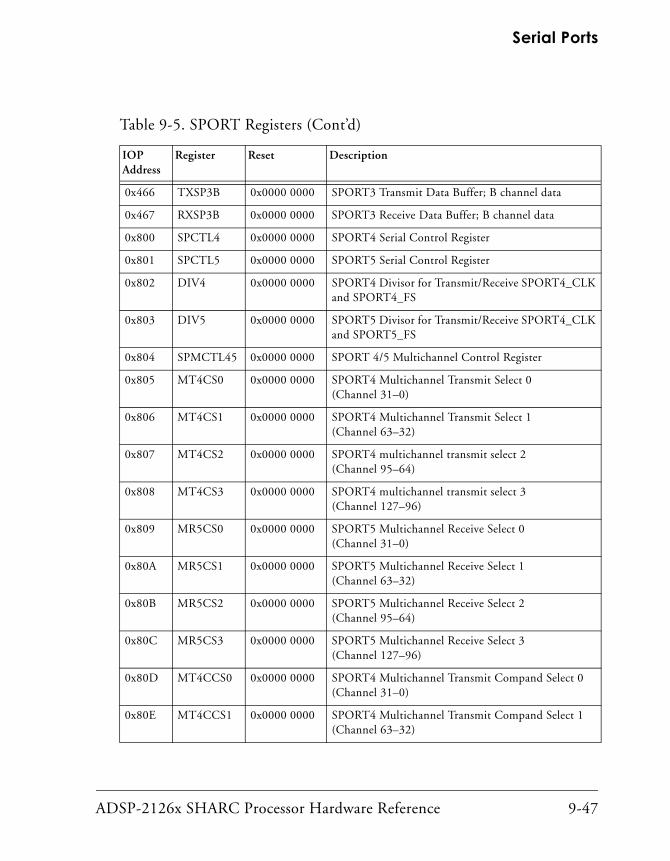
ADSP-2126x SHARC Processor Hardware Reference 9-47
Serial Ports
0x466 TXSP3B 0x0000 0000 SPORT3 Transmit Data Buffer; B channel data
0x467 RXSP3B 0x0000 0000 SPORT3 Receive Data Buffer; B channel data
0x800 SPCTL4 0x0000 0000 SPORT4 Serial Control Register
0x801 SPCTL5 0x0000 0000 SPORT5 Serial Control Register
0x802 DIV4 0x0000 0000 SPORT4 Divisor for Transmit/Receive SPORT4_CLK and SPORT4_FS
0x803 DIV5 0x0000 0000 SPORT5 Divisor for Transmit/Receive SPORT4_CLK and SPORT5_FS
0x804 SPMCTL45 0x0000 0000 SPORT 4/5 Multichannel Control Register
0x805 MT4CS0 0x0000 0000 SPORT4 Multichannel Transmit Select 0 (Channel 31–0)
0x806 MT4CS1 0x0000 0000 SPORT4 Multichannel Transmit Select 1 (Channel 63–32)
0x807 MT4CS2 0x0000 0000 SPORT4 multichannel transmit select 2 (Channel 95–64)
0x808 MT4CS3 0x0000 0000 SPORT4 multichannel transmit select 3 (Channel 127–96)
0x809 MR5CS0 0x0000 0000 SPORT5 Multichannel Receive Select 0 (Channel 31–0)
0x80A MR5CS1 0x0000 0000 SPORT5 Multichannel Receive Select 1(Channel 63–32)
0x80B MR5CS2 0x0000 0000 SPORT5 Multichannel Receive Select 2 (Channel 95–64)
0x80C MR5CS3 0x0000 0000 SPORT5 Multichannel Receive Select 3 (Channel 127–96)
0x80D MT4CCS0 0x0000 0000 SPORT4 Multichannel Transmit Compand Select 0 (Channel 31–0)
0x80E MT4CCS1 0x0000 0000 SPORT4 Multichannel Transmit Compand Select 1 (Channel 63–32)
Table 9-5. SPORT Registers (Cont’d)
IOP Address
Register Reset Description

SPORT Control Registers and Data Buffers
9-48 ADSP-2126x SHARC Processor Hardware Reference
0x80F MT4CCS2 0x0000 0000 SPORT4 Multichannel Transmit Compand Select 2 (Channel 95–64)
0x810 MT4CCS3 0x0000 0000 SPORT4 Multichannel Transmit Compand Select 3 (Channel 127–96)
0x811 MR5CCS0 0x0000 0000 SPORT5 Multichannel Receive Compand Select 0(Channel 31–0)
0x812 MR5CCS1 0x0000 0000 SPORT5 Multichannel Receive Compand Select 1 (Channel 63–32)
0x813 MR5CCS2 0x0000 0000 SPORT5 Multichannel Receive Compand Select 2 (Channel 95–64)
0x814 MR5CCS3 0x0000 0000 SPORT5 Multichannel Receive Compand Select 3 (Channel 127–96)
0x860 TXSP4A 0x0000 0000 SPORT4 Transmit Data Buffer; A channel data
0x861 RXSP4A 0x0000 0000 SPORT4 Receive Data Buffer; A channel data
0x862 TXSP4B 0x0000 0000 SPORT4 Transmit Data Buffer; B channel data
0x863 RXSP4B 0x0000 0000 SPORT4 Receive Data Buffer; B channel data
0x864 TXSP5A 0x0000 0000 SPORT5 Transmit Data Buffer; A channel data
0x865 RXSP5A 0x0000 0000 SPORT5 Receive Data Buffer; A channel data
0x866 TXSP5B 0x0000 0000 SPORT5 Transmit Data Buffer; B channel data
0x867 RXSP5B 0x0000 0000 SPORT5 Receive Data Buffer; B channel data
0xC00 SPCTL0 0x0000 0000 SPORT0 Serial Control Register
0xC01 SPCTL1 0x0000 0000 SPORT1 Serial Control Register
0xC02 DIV0 0x0000 0000 SPORT0 Divisor for Transmit/Receive SPORT0_CLK and SPORT0_FS
0xC03 DIV1 0x0000 0000 SPORT1 Divisor for Transmit/Receive SPORT1_CLK and SPORT1_FS
0xC04 SPMCTL01 0x0000 0000 SPORT 0/1 Multichannel Control Register
Table 9-5. SPORT Registers (Cont’d)
IOP Address
Register Reset Description

ADSP-2126x SHARC Processor Hardware Reference 9-49
Serial Ports
0xC05 MT0CS0 0x0000 0000 SPORT0 Multichannel Transmit Select 0 (Channels 31–0)
0xC06 MT0CS1 0x0000 0000 SPORT0 Multichannel Transmit Select 1 (Channels 63–32)
0xC07 MT0CS2 0x0000 0000 SPORT0 Multichannel Transmit Select 2 (Channels 95–64)
0xC08 MT0CS3 0x0000 0000 SPORT0 Multichannel Transmit Select 3 (Channels 127–96)
0xC09 MR1CS0 0x0000 0000 SPORT1 Multichannel Receive Select 0 (Channels 31–0)
0xC0A MR0CS1 0x0000 0000 SPORT0 Multichannel Receive Select 1 (Channels 63–32)
0xC0B MR0CS2 0x0000 0000 SPORT0 Multichannel Receive Select 2 (Channels 95–64)
0xC0C MR1CS3 0x0000 0000 SPORT0 Multichannel Receive Select 3(Channels 127–96)
0xC0D MT0CCS0 0x0000 0000 SPORT0 Multichannel Transmit Compand Select 0 (Channels 31–0)
0xC0E MT0CCS1 0x0000 0000 SPORT0 Multichannel Transmit Compand Select 1 (Channels 63–32)
0xC0F MT0CCS2 0x0000 0000 SPORT0 multichannel transmit compand select 2 (Channels 95–64)
0xC10 MT0CCS3 0x0000 0000 SPORT0 Multichannel Transmit Compand Select 3 (Channels 127–96)
0xC11 MR1CCS0 0x0000 0000 SPORT1 Multichannel Receive Compand Select 0 (Channels 31–0)
0xC12 MR1CCS1 0x0000 0000 SPORT1 Multichannel Receive Compand Select 1 (Channels 63–32)
0xC13 MR1CCS2 0x0000 0000 SPORT1 Multichannel Receive Compand Select 2 (Channels 95–64)
Table 9-5. SPORT Registers (Cont’d)
IOP Address
Register Reset Description

SPORT Control Registers and Data Buffers
9-50 ADSP-2126x SHARC Processor Hardware Reference
Register Writes and Effect LatencySPORT register writes are internally completed at the end of three (worst case) or two (best case) core clock cycles. The newly written value to the SPORT register can be read back on the next cycle. Reads of the SPORT registers take four core clock cycles.
After a write to a SPORT register, control and mode bit changes take effect in the second serial clock cycle. The serial ports are ready to start transmitting or receiving three serial clock cycles after they are enabled in the SPCTLx control register. No serial clocks are lost from this point on.
Serial Port Control Registers (SPCTLx)The main control register for each serial port is the Serial Port Control register, SPCTLx. These registers are described in “SPORT Serial Control Registers (SPCTLx)” on page A-68. When changing operating modes,
0xC14 MR1CCS3 0x0000 0000 SPORT1 Multichannel Receive Compand select 3 (Channels 127–96)
0xC60 TXSP0A 0x0000 0000 SPORT0 Transmit Data Buffer; A channel data
0xC61 RXSP0A 0x0000 0000 SPORT0 Receive Data Buffer; A channel data
0xC62 TXSP0B 0x0000 0000 SPORT0 Transmit Data Buffer; B channel data
0xC63 RXSP0B 0x0000 0000 SPORT0 Receive Data Buffer; B channel data
0xC64 TXSP1A 0x0000 0000 SPORT1 Transmit Data Buffer; A channel data
0xC65 RXSP1A 0x0000 0000 SPORT1 Receive Data Buffer; A channel data
0xC66 TXSP1B 0x0000 0000 SPORT1 Transmit Data Buffer; B channel data
0xC67 RXSP1B 0x0000 0000 SPORT1 Receive Data Buffer; B channel data
Table 9-5. SPORT Registers (Cont’d)
IOP Address
Register Reset Description

ADSP-2126x SHARC Processor Hardware Reference 9-51
Serial Ports
clear the Serial Port Control register before the new mode is written to the register.
There is one Global Control and Status register for each paired SPORT (SPORT0/1, SPORT 2/3 and SPORT 4/5) for multichannel operation. These are SPMCTL01, SPMCTL23, or SPMCTL45. These registers define the number of channels, provide the status of the current channel, enable multichannel operation, and set the multichannel frame delay. These reg-isters are described in “SPORT Multichannel Control Registers (SPMCTLxy)” on page A-77.
The SPCTLx registers control the operating modes of the serial ports for the I/O processor. Table 9-6 lists all the bits in the SPCTLx register.
Table 9-6. SPCTLx Control Bit Comparison in Four SPORT Operation Modes
BitStandard DSP Serial Mode
Left-justified and I2S Sample Pair Mode
Multichannel Mode
Transmit Control Bits (SPORT0, 2, and 4)
Receive Control Bits (SPORT1, 3, and 5)
0 SPEN_A SPEN_A Reserved Reserved
1 DTYPE Reserved DTYPE DTYPE
2 DTYPE Reserved DTYPE DTYPE
3 LSBF Reserved LSBF LSBF
4 SLEN0 SLEN0 SLEN0 SLEN0
5 SLEN1 SLEN1 SLEN1 SLEN1
6 SLEN2 SLEN2 SLEN2 SLEN2
7 SLEN3 SLEN3 SLEN3 SLEN3
8 SLEN4 SLEN4 SLEN4 SLEN4
9 PACK PACK PACK PACK
10 ICLK MSTR Reserved ICLK
11 OPMODE OPMODE OPMODE OPMODE

SPORT Control Registers and Data Buffers
9-52 ADSP-2126x SHARC Processor Hardware Reference
12 CKRE Reserved CKRE CKRE
13 FSR Reserved Reserved Reserved
14 IFS Reserved Reserved IMFS
15 DIFS DIFS Reserved Reserved
16 LFS FRFS LTDV LRFS
17 LAFS LAFS Reserved Reserved
18 SDEN_A SDEN_A SDEN_A SDEN_A
19 SCHEN_A SCHEN_A SCHEN_A SCHEN_A
20 SDEN_B SDEN_B SDEN_B SDEN_B
21 SCHEN_B SCHEN_B SCHEN_B SCHEN_B
22 FS_BOTH Reserved Reserved Reserved
23 BHD BHD BHD BHD
24 SPEN_B SPEN_B Reserved Reserved
25 SPTRAN SPTRAN Reserved Reserved
26 ROVF_B, or TUVF_B
ROVF_B, or TUVF_B TUVF_B ROVF_B
27 DXS_B DXS_B TXS_B RXS_B
28 DXS_B DXS_B TXS_B RXS_B
29 ROVF_A, or TUVF_A
ROVF_A, or TUVF_A TUVF_A ROVF_A
30 DXS_A DXS_A TXS_A RXS_A
31 DXS_A DXS_A TXS_A RXS_A
Table 9-6. SPCTLx Control Bit Comparison in Four SPORT Operation Modes (Cont’d)
BitStandard DSP Serial Mode
Left-justified and I2S Sample Pair Mode
Multichannel Mode
Transmit Control Bits (SPORT0, 2, and 4)
Receive Control Bits (SPORT1, 3, and 5)

ADSP-2126x SHARC Processor Hardware Reference 9-53
Serial Ports
The following bits, listed in bit number order, control serial port modes and are part of the SPCTLx (transmit and receive) Control registers. Other bits in the SPCTLx registers set up DMA and I/O processor-related serial port features. For information about configuring a specific operation mode, refer to Table 9-1 on page 9-10 and “Standard DSP Serial Mode” on page 9-11.
Serial Port Enable. SPCTLx bits 0 and 24 (SPEN_A and SPEN_B). This bit enables (if set, = 1) or disables (if cleared, = 0) the corresponding serial port channel A or B. Clearing this bit aborts any ongoing operation and clears the status bits. The SPORTS are ready to transmit or receive two serial clock cycles after enabling.
This description applies to I2S and DSP Standard Serial modes only.
Data Type Select. SPCTLxx bits 2–1 (DTYPE). These bits select the com-panding and MSB data type formatting of serial words loaded into the transmit and receive buffers. This bit applies to DSP standard Serial and Multichannel modes only. The Transmit Shift register does not zero-fill or sign-extend transmit data words; this only takes place for the receive shift register.
For Standard mode, selection of Companding mode and MSB format are exclusive:
00 = Right-justify; fill unused MSBs with 0s01 = Right-justify; sign-extend into unused MSBs10 = Compand using μ_law, (primary channels only)11 = Compand using A_law, (primary channels only)
For Multichannel mode, selection of companding mode and MSB format are independent:
x0 = Right-justify; fill unused MSBs with 0sx1 = Right-justify; sign-extend into unused MSBs0x = Compand using μ_law 1x = Compand using A_law
SPORT Control Registers and Data Buffers
9-54 ADSP-2126x SHARC Processor Hardware Reference
This description applies only to DSP Standard Serial mode and Multi-channel modes only.
Serial Word Endian Select. SPCTLx Bit 3 (LSBF). This bit selects little endian words (LSB first, if set, = 1) or big endian words (MSB first, if cleared, = 0). This description applies to DSP Standard Serial And Multi-channel modes only.
Serial Word Length Select. SPCTLx Bit 8–4 (SLENx). These bits select the word length in bits. Word sizes can be from 3 bits (SLEN = 2) to 32 bits (SLEN = 31). This bit applies to all operation modes.
Use this formula to calculate the value for SLEN:
SLEN = Actual serial word length – 1
In this case, the SLEN bit cannot equal 0 or 1, I2S, Left-justified Sample Pair word length is limited to 8-32 bits, and DSP Standard mode word length varies from 3 to 32 bits.
16-bit to 32-bit Word Packing Enable. SPCTLx bit 9 (PACK). This bit enables (if set, = 1) or disables (if cleared, = 0) 16- to 32-bit word packing. This bit applies to all operation modes.
Internal Clock Select. SPCTLx bit 10 (ICLK). This bit selects the internal (if set, =1) or external (if cleared, =0) transmit or receive clock. This bit applies to DSP Standard Serial mode and SPORTs 1, 3 and 5 for multi-channel modes.
Sport Operation Mode. SPCTLx bit 11 (OPMODE). This bit enables
I2S/Left-justified Sample Pair modes if set (= 1), or disables if cleared (= 0). This bit applies to all operation modes. See Table 9-1 on page 9-10 and “Standard DSP Serial Mode” on page 9-11.
Clock Rising Edge Select. SPCTLx bit 12 (CKRE). This bit selects whether the serial port uses the rising edge (if set, = 1) or falling edge (if cleared,

ADSP-2126x SHARC Processor Hardware Reference 9-55
Serial Ports
= 0) of the clock signal for sampling data and the frame sync. This bit applies to DSP Standard Serial and Multichannel modes only.
Frame Sync Required Select. SPCTLx bits 13 (FSR). This bit selects whether the serial port requires (if set, = 1) or does not require (if cleared, = 0) a transfer frame sync. See “Frame Sync Options” on page 9-34 for more details. This bit applies to DSP Standard Serial mode only.
Internal Frame Sync Select. SPCTLx bit 14 (IFS). This bit selects whether the serial port uses an internally-generated frame sync (if set, = 1) or a frame sync from an external (if cleared, = 0) source. This bit is used for Standard DSP Serial mode only.
Low Active Frame Sync Select. SPCTLx bit 16 (LFS). This bit selects the logic level of the (transmit or receive) frame sync signals. This bit selects an active low frame sync (if set, = 1) or active high frame sync (if cleared, = 0). Active high (0) is the default. This bit applies to DSP Standard Serial mode only.
Late Transmit Frame Sync Select. SPCTLx bit 17 (LAFS). This bit selects when to generate the frame sync signal. This bit selects a late frame sync if set (= 1) during the first bit of each data word. This bit selects an early frame sync if cleared (= 0) during the serial clock cycle immediately pre-ceding the first data bit. See “Frame Sync Options” on page 9-34 for more details.
This bit applies to DSP Standard Serial mode. This bit is also used to
select between I2S and Left-justified Sample Pair modes. See Table 9-1 on page 9-10 and “Standard DSP Serial Mode” on page 9-11 for more information.
Serial Port DMA Enable. SPCTLx bits 18 and 20 (SDEN_A and SDEN_B). This bit enables (if set, = 1) or disables (if cleared, = 0) the serial port’s channel DMA. Bits 18 and 20 apply to all operating modes.
Serial Port DMA Chaining Enable. SPCTLx bits 19 and 21 (SCHEN_A and SCHEN_B). These bits enable (if set, = 1) or disables (if cleared, = 0) serial

SPORT Control Registers and Data Buffers
9-56 ADSP-2126x SHARC Processor Hardware Reference
port’s channels A and B DMA chaining. Bits 19 and 21 apply to all oper-ating modes.
Frame Sync Both Enable. SPCTLx bit 22 (FS_BOTH). This bit applies when the SPORTS channels A and B are configured to transmit/receive data. If set (= 1), this bit issues frame sync only when data is present in both trans-mit buffers, TXA and TXB. If cleared (= 0), a frame sync is issued if data is present in either transmit buffers. This bit applies to DSP Standard Serial mode only.
When a SPORT is configured as a receiver, if FS_BOTH is set (= 1), frame sync is issued only when both the Rx FIFOs (RXSPA and RXSPB) are not full.
This bit is not used for I2S and Left-justified Sample Pair modes. If only channel A or channel B is selected, the frame sync behaves as if FS_BOTH is cleared (= 0). If both A and B channels are selected, the word select acts as if FS_BOTH is set (= 1).
Buffer Hang Disable. SPCTLx bit 23 (BHD). When cleared (= 0), this bit causes the processor core to hang when it attempts to write to a full buffer or read from an empty buffer. When set (= 1), this bit disables the core-hang. In this case, a core read from an empty receive buffer returns previously-read (invalid) data and core writes to a full transmit buffer to overwrite (valid) data that has not yet been transmitted. This bit is used in all modes.
Data Direction Control. SPCTLx bit 25 (SPTRAN). This bit controls the data direction of the serial port channel A and B signals.
• 0 = SPORT is configured to receive on both channels A and B. In this configuration, the RXSPxA and RXSPxB buffers are activated, while the Receive Shift registers are controlled by SPORTx_CLK and SPORTx_FS. The TXSPxA and TXSPxB buffers are inactive.

ADSP-2126x SHARC Processor Hardware Reference 9-57
Serial Ports
• 1 = SPORT is configured to transmit on both channels A and B. In this configuration, the TXSPxA and TXSPxB buffers are activated, while the Transmit Shift registers are controlled by SPORTx_CLK and SPORTx_FS. The RXSPxA and RXSPxB buffers are inactive.
This bit applies to I2S, Left-justified Sample Pair, and DSP Standard Serial modes.
Reading from or writing to inactive buffers cause the core to hang indefinitely until the SPORT is cleared.
Data Buffer Error Status (sticky, read-only). SPCTLx bit 29 and 26 (ROVF, TUVF). These bits indicate whether the serial transmit operation has under-flowed (if set, = 1 and SPTRAN = 1) or a receive operation has overflowed (if set, = 1 and SPTRAN = 0) in the TXSPxA/RXSPxA and TXSPxB/RXSPxB data buffers.
This description applies to I2S, Left-justified Sample Pair, and DSP Stan-dard Serial modes. In multichannel modes, corresponding bits (TUVF, ROVF) are used for this function.
When the SPORT is configured as a transmitter, this bit provides transmit underflow status. As a transmitter, if FSR = 1, this bit indicates whether the SPORTx_FS signal (from an internal or external source) occurred while the DXS buffer was empty. If FSR = 0, ROVF or TUVF is set whenever the SPORT is required to transmit and the transmit buffer is empty. The SPORTs transmit data whenever they detect a SPORTx_FS signal.
• 0 = No SPORTx_FS signal occurred while TXSPxA/B buffer is empty.
• 1 = SPORTx_FS signal occurred while TXSPxA/B buffer is empty.
SPORT Control Registers and Data Buffers
9-58 ADSP-2126x SHARC Processor Hardware Reference
When the SPORT is configured as a receiver, these bits provide receive overflow status. As a receiver, it indicates when the channel has received new data while the RXS_A buffer is full. New data overwrites existing data.
• 0 = No new data while RXSPxA/B buffer is full.
• 1 = New data while RXSPxA/B buffer is full.
Transmit Underflow Status (sticky, read-only). SPCTL0, SPCTL2, and SPCTL4 bit 29 (TUVF_A). This bit indicates (if set, = 1) whether the multi-channel SPORTx_FS signal (from an internal or external source) occurred while the TXS buffer was empty. SPORTs transmit data whenever they detect a SPORTx_FS signal. If cleared (= 0), no SPORTx_FS signal occurs because the TXS buffer is empty.
The Transmit Underflow Status bit (TUVF_A/ROVF_A or TUVF_A and TUVF_B/ROVF_B or TUVF_B) is set when the SPORTx_FS signal occurs from either an external or internal source while the TXSPxA or TXSPxB buffer is empty. The internally-generated SPORTx_FS signal may be suppressed whenever TXSPxA or TXSPxB is empty by clearing the DIFS control bit when SPTRAN = 1.
When the DIFS bit is cleared (the default setting) the frame sync signal (SPORTx_FS) is dependent upon new data being present in the transmit buffer. The SPORTx_FS signal is only generated for new data. Setting DIFS to 1 selects data-independent frame syncs which causes the SPORTx_FS sig-nal to be generated whether or not new data is present. With each SPORTx_FS signal, the SPORT transmits the contents of the transmit buf-fer. Serial port DMA typically keeps the transmit buffer full.
The DIFS bit applies to Multichannel mode only when the SPORTs are configured as transmitters.
Receive Overflow Status (read-only, sticky). SPCTL1, SPCTL3 and SPCTL5 Bit 29 (ROVF). This bit indicates if the channel has received new data if set (=1) or not if cleared (=0) while the RXS_A/B buffer is full. New data over-writes existing data.

ADSP-2126x SHARC Processor Hardware Reference 9-59
Serial Ports
This bit applies to Multichannel mode only.
Data Buffer Status Channel A (read-only). SPCTL1, SPCTL3 and SPCTL5 bits 31–30 (RXS_A). These bits indicate the status of the channel’s receive buffer contents as follows: 00 = buffer empty, 01 = reserved, 10 = buffer partially full, 11 = buffer full.
DXS Data Buffer Status. SPCTLx Bits 31–30 (DXS_A) and bits 28-27 (DXS_B). These read-only bits indicate the status of the serial port’s data buffer as follows: 11 = buffer full, 00 = buffer empty, 10 = buffer partially full, 01 = reserved.
The DXS_A or DXS_B Status bits indicate whether the TXSPxA/RXSPxA or TXSPxB/RXSPxB buffer is full (11), empty (00), or partially full (10). To test for space in TXSPxA/B or RXSPxA/B, test whether DXS_A (bit 30) is equal to zero for the A channel, or whether DXS_B (bit 27) is equal to zero for the B channel. To test for the presence of any data in TXSPxA/B or RXSPxA/B, test whether DXS_A (bit 31) is equal to one for the A channel, or whether DXS_B (bit 28) is equal to one for the B channel.
This description applies to I2S, Left-justified Sample Pair, and DSP Stan-dard Serial modes.
When the SPORT is configured as a transmitter, these bits reflect transmit buffer status for the TXSPxA and TXSPxB buffers. When the SPORT is configured as a receiver, these bits reflect receive buffer status for the RXSPxA and RXSPxB buffers.
Transmit Data Buffer Status (read-only). SPCTL0, SPCTL2 and SPCTL4 Bits 30 and 31(TXS_A). These bits indicate the status of the serial port chan-nel’s transmit buffer as follows: 11 = buffer full, 00 = buffer empty, 10 = buffer partially full.

SPORT Control Registers and Data Buffers
9-60 ADSP-2126x SHARC Processor Hardware Reference
Transmit and Receive Data BuffersThe transmit buffers (TXSP0A, TXSP0B, TXSP1A, TXSP1B, TXSP2A, TXSP2B, TXSP3A, TXSP3B, TXSP4A, TXSP4B, TXSP5A, and TXSP5B) are the 32-bit trans-mit data buffers for SPORT0, SPORT1, SPORT2, SPORT3, SPORT4, and SPORT5 respectively. These buffers must be loaded with the data to be transmitted if the SPORT is configured to transmit on the A and B channels. The data is loaded automatically by the DMA controller or loaded manually by the program running on the processor core.
The receive buffers (RXSP0A, RXSP0B, RXSP1A, RXSP1B, RXSP2A, RXSP2B, RXSP3A, RXSP3B, RXSP4A, RXSP4B, RXSP5A, and RXSP5B) are the 32-bit receive data buffers for SPORT0, SPORT1, SPORT2, SPORT3, SPORT4, and SPORT5 respectively. These 32-bit buffers become active when the SPORT is configured to receive data on the A and B channels. When a SPORT is configured as a receiver, the RXSPxA and RXSPxB regis-ters are automatically loaded from the receive shifter when a complete word has been received. The data is then loaded to internal memory by the DMA controller or read directly by the program running on the processor core.
Word lengths of less than 32 bits are automatically right-justified in the receive and transmit buffers.
The transmit buffers act like a two-location FIFO because they have a data register plus an Output Shift register. Two 32-bit words may both be stored in the transmit queue at any one time. When the transmit register is loaded and any previous word has been transmitted, the register contents are automatically loaded into the output shifter. An interrupt occurs when the Output Transmit shifter has been loaded, signifying that the transmit buffer is ready to accept the next word (for example, the transmit buffer is not full). This interrupt does not occur when serial port DMA is enabled or when the corresponding mask bit in the LIRPTL register is set.
In non-Multichannel modes (I2S, Left-justified Sample Pair, and DSP Standard Serial modes), the ROVF_A or TUVF_A and ROVF_B, or TUVF_B

ADSP-2126x SHARC Processor Hardware Reference 9-61
Serial Ports
Overflow/Underflow status bits are set when an overflow or underflow occurs. In multichannel mode, the ROVF_A or TUVF_A bits are redefined due to the fixed-directional functionality of the SPCTLx registers. When the SPCTL1, SPCTL3 and SPCTL5 registers are configured for Multichannel mode, the Receive Overflow bit ROVF_A indicates when the A channel has received new data while the RXS_A buffer is full. Similarly, when the SPCTL0, SPCTL2 and SPCTL4 registers are configured for Multichannel mode, the transmit overflow bit (TUVF_A) indicates that a new frame sync signal (SPORT0_FS/SPORT2_FS/SPORT4_FS) was generated while the TXSPxA buffer was empty.
The ROVF_A or TUVF_A (bit 29) Overflow/Underflow status bit in the SPCTLx register becomes fixed in Multichannel mode only as either the ROVF Overflow Status bit (SPORTs 1, 3, and 5) or TUVF_A Underflow Status bit (SPORTs 0, 2, and 4).
When the SPORT is configured as a transmitter (SPTRAN =1), and a trans-mit frame sync occurs and no new data has been loaded into the transmit buffer, a Transmit Underflow status bit is set in the Serial Port Control register. The TUVF_A/ROVF_A or TUVF_A status bit is sticky and is only cleared by disabling the serial port.
When the SPORT is configured as a receiver (SPTRAN = 0), the receive buf-fers are activated. The receive buffers act like a three-location FIFO because they have two data registers plus an input shift register. Two com-plete 32-bit words can be stored in the receive buffer while a third word is being shifted in. The third word overwrites the second if the first word has not been read out (by the processor core or the DMA controller). When this happens, the Receive Overflow Status bit is set in the Serial Port Con-trol register. Almost three complete words can be received without the receive buffer being read before an overflow occurs. The overflow status is generated on the last bit of the third word. The ROVF_A/ROVF_A or TUVF_A status bit is sticky and is cleared only by disabling the serial port.
An interrupt is generated when the receive buffer has been loaded with a received word (for example, the receive buffer is not empty). This inter-

SPORT Control Registers and Data Buffers
9-62 ADSP-2126x SHARC Processor Hardware Reference
rupt is masked if serial port DMA is enabled or if the corresponding bit in the LIRPTL register is set.
If your program causes the core processor to attempt to read from an empty receive buffer or to write to a full transmit buffer, the access is delayed until the buffer is accessed by the external I/O device. This delay is called a core processor hang. If you do not know if the core processor can access the receive or transmit buffer without a hang, the buffer’s status should be read first (in SPCTLx) to determine if the access can be made.
To support debugging buffer transfers, the processor has a Buffer Hang Disable (BHD) bit. When set (= 1), this bit prevents the pro-cessor core from detecting a buffer-related stall condition, permitting debugging of this type of stall condition. For more information, see the BHD bit description on on page 9-56.
The status bits in SPCTLx are updated during reads and writes from the core processor even when the serial port is disabled. Disable the serial port when writing to the receive buffer or reading from the transmit buffer.
When programming the serial port channel (A or B) as a transmit-ter, only the corresponding TXSPxA and TXSPxB buffers become active while the receive buffers RXSPxA and RXSPxB remain inactive. Similarly, when the SPORT channel A and B are programmed as receive-only the corresponding RXSPxA and RXSPxB is activated. Do not attempt to read or write to inactive data buffers. If the proces-sor operates on the inactive transmit or receive buffers while the SPORT is enabled, unpredictable results may occur.
Clock and Frame Sync Frequencies (DIV)The DIVx registers contain divisor values that determine frequencies for internally-generated clocks and frame syncs. The DIVx registers are described in Appendix A in “SPORT Divisor Registers (DIVx)” on page A-84.

ADSP-2126x SHARC Processor Hardware Reference 9-63
Serial Ports
The CLKDIV bit field specifies how many times the processor’s internal clock (CCLK) is divided to generate the transmit and receive clocks. The frame sync (SPORTx_FS) is considered a receive frame sync if the data sig-nals are configured as receivers. Likewise, the frame sync SPORTx_FS is considered a transmit frame sync if the data signals are configured as transmitters. The divisor is a 15-bit value, allowing a wide range of serial clock rates.
Use the following equation to calculate the serial clock frequency:
The maximum serial clock frequency is equal to one-quarter the proces-sor’s internal clock (CCLK) frequency, which occurs when CLKDIV is set to zero. Use the following equation to determine the value of CLKDIV, given the CCLK frequency and desired serial clock frequency:
The bit field FSDIV specifies how many transmit or receive clock cycles are counted before a frame sync pulse is generated. In this way, a frame sync
Figure 9-8. DIVx Register
fSPORTx_CLK = fCCLK4(CLKDIV+1)
4(fSPORTx_CLK)
fCCLK – 1 CLKDIV =
31 30 29 28 27 26 24 23 22 21 20 19 18 17 16
00 0 0 0 0 0 0 0 0 0 0 0 0 0 0
FSDIV
15 14 13 12 11 10 8 7 6 5 4 3 2 1 0
00 0 0 0 0 0 0 0 0 0 0 0 0 0 0
CLKDIVClock Divisor
25
9
Frame Sync Divis
Reserved
DIV0 (0xC02)DIV1 (0xC03)DIV2 (0x402)DIV3 (0x403)DIV4 (0x802)DIV5 (0x803)

SPORT Control Registers and Data Buffers
9-64 ADSP-2126x SHARC Processor Hardware Reference
can initiate periodic transfers. The counting of serial clock cycles applies to internally- or externally-generated serial clocks.
The formula for the number of cycles between frame sync pulses is:# of serial clocks between frame syncs = FSDIV + 1
Use the following equation to determine the value of FSDIV, given the serial clock frequency and desired frame sync frequency:
The frame sync is continuously active when FSDIV = 0. The value of FSDIV should not be less than the serial word length minus one (the value of the SLEN field in the Serial Port Control register), as this may cause an external device to abort the current operation or cause other unpredictable results. If the serial port is not being used, the FSDIV divisor can be used as a coun-ter for dividing an external clock or for generating a periodic pulse or periodic interrupt. The serial port must be enabled for this mode of oper-ation to work properly.
Exercise caution when operating with externally-generated transmit clocks near the frequency of one-quarter of the processor’s internal clock. There is a delay between when the clock arrives at the SPORTx_CLK node and when data is output. This delay may limit the receiver’s speed of opera-tion. Refer to the data sheet for exact timing specifications.
Externally-generated late transmit frame syncs also experience a delay from when they arrive to when data is output. This can also limit the max-imum serial clock speed. Refer to the product specific data sheet for exact timing specifications.
SPORT InterruptsEach serial port has an interrupt associated with it. For each SPORT, both the A and B channel transmit and receive data buffers share the same
fSPORTx_CLKfSPORTx_FS
– 1FSDIV =

ADSP-2126x SHARC Processor Hardware Reference 9-65
Serial Ports
interrupt vector. The interrupts can be used to indicate the completion of the transfer of a block of serial data when the serial ports are configured for DMA. They can also be used to perform single word transfers. Refer to “Single Word Transfers” on page 9-73. The priority of the serial port interrupts is shown in Table 9-7.
The interrupt names are defined in the def2126x.h file supplied with the ADSP-21xxx processor’s Development Software.
SPORT interrupts occur on the second coreclock (CCLK) after the last bit of the serial word is latched in or driven out.
Moving Data Between SPORTS and Internal Memory
Transmit and receive data can be transferred between the serial ports and on-chip memory with single word transfers or with DMA block transfers. Both methods are interrupt-driven, and use the same internally-generated interrupts.
SPORT DMA provides a mechanism for receiving or transmitting an entire block of serial data before the interrupt is generated. When serial
Table 9-7. Priority of the Serial Port Interrupts
Interrupt Name Interrupt
SPR1I SPORT1 DMA Channels (Highest Priority)
SPR3I SPORT3 DMA Channels
SPR5I SPORT5 DMA Channels
SPR0I SPORT0 DMA Channels
SPR2I SPORT2 DMA Channels
SPR4I SPORT4 DMA Channels

Moving Data Between SPORTS and Internal Memory
9-66 ADSP-2126x SHARC Processor Hardware Reference
port DMA is not enabled, the SPORT generates an interrupt every time it receives or starts to transmit a data word. The processor’s on-chip DMA controller handles the DMA transfer, allowing the processor core to con-tinue running until the entire block of data is transmitted or received. Service routines can then operate on the block of data rather than on sin-gle words, significantly reducing overhead.
Standard DMA does not function properly in I2S/left-justified mode when two channels (A and B) are enabled with different DMA count values. In this case, the interrupt is generated for the least (smallest) count only. If both the A and B channels of the SPORTs are used in I2S/left-justified mode with DMA enabled, then the DMA count value should be the same for both channels. This does not apply to chained DMA.
DMA Block TransfersThe processor’s on-chip DMA controller allows automatic DMA transfers between internal memory and each of the two channels of each serial port. Each SPORT has two channels for transferring data, and each can be con-figured to receive or to transmit. There are twelve DMA channels for serial port operations. The serial port DMA channels are numbered as shown in Table 9-8.

ADSP-2126x SHARC Processor Hardware Reference 9-67
Serial Ports
Data-direction programmability is supported in Standard DSP Standard
Serial, Left-justified Sample Pair, and I2S modes. The value of the SPTRAN bit in SPCTLx (0 = RX, 1 = TX) determines whether the receive or transmit register for the SPORT becomes active.
The SPORT DMA channels are assigned higher priority than all other DMA channels (for example, the SPI port and the parallel port) because of their relatively low service rate and their inability to hold off incoming data. Having higher priority causes the SPORT DMA transfers to be per-formed first when multiple DMA requests occur in the same cycle.
Although the DMA transfers are performed with 32-bit words, serial ports
can handle word sizes from 3 to 32 bits, with 8 to 32 bits for I2S mode. If serial words are 16 bits or smaller, they can be packed into 32-bit words for each DMA transfer. DMA transfers are configured using the PACK bit in the SPCTLx Control registers. When serial port data packing is enabled
Table 9-8. Serial Port DMA Channels
Channel Data Buffer Description Priority
0 RXSP1A/TXSP1A SPORT1 A data Highest
1 RXSP1B/TXSP1B SPORT1 B data
2 RXSP0A/TXSP0A SPORT0 A data
3 RXSP0B/TXSP0B SPORT0 B data
4 RXSP3A/TXSP3A SPORT3 A data
5 RXSP3B/TXSP3B SPORT3 B data
6 RXSP2A/TXSP2A SPORT2 A data
7 RXSP2B/TXSP2B SPORT2 B data
8 RXSP5A/TXSP5A SPORT5 A data
9 RXSP5B/TXSP5B SPORT5 B data
10 RXSP4A/TXSP4A SPORT4 A data
11 RXSP4B/TXSP4B SPORT4 B data Lowest

Moving Data Between SPORTS and Internal Memory
9-68 ADSP-2126x SHARC Processor Hardware Reference
(PACK = 1), the transmit and receive interrupts are generated for the 32-bit packed words, not for each 16-bit word.
The following sections present an overview of serial port DMA operations; additional details are covered in the“Memory” in Chapter 5, Memory.
• For information on SPORT DMA Channel Setup, see “Selecting Transmit and Receive Channel Order (FRFS)” on page 9-16.
• For information on SPORT DMA Parameter Registers, see “Select-ing Transmit and Receive Channel Order (FRFS)” on page 9-16.
• For information on SPORT DMA Chaining, see “SPORT DMA Chaining” on page 9-73.
Setting Up DMA on SPORT Channels
Each SPORT DMA channel has an Enable bit (SDEN_A and SDEN_B) in its SPCTLx Control register. When DMA is disabled for a particular channel, the SPORT generates an interrupt every time it receives a data word or whenever there is a vacancy in the transmit buffer. For more information, see “Single Word Transfers” on page 9-73.
Each channel also has a DMA Chaining Enable bit (SCHEN_A and SCHEN_B) in its SPCTLx control register.
To set up a serial port DMA channel, write a set of memory buffer param-eters to the SPORT DMA parameter registers as shown in Table 9-9.
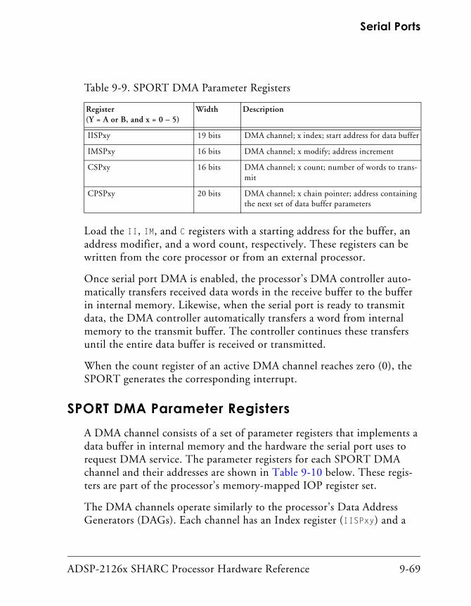
ADSP-2126x SHARC Processor Hardware Reference 9-69
Serial Ports
Load the II, IM, and C registers with a starting address for the buffer, an address modifier, and a word count, respectively. These registers can be written from the core processor or from an external processor.
Once serial port DMA is enabled, the processor’s DMA controller auto-matically transfers received data words in the receive buffer to the buffer in internal memory. Likewise, when the serial port is ready to transmit data, the DMA controller automatically transfers a word from internal memory to the transmit buffer. The controller continues these transfers until the entire data buffer is received or transmitted.
When the count register of an active DMA channel reaches zero (0), the SPORT generates the corresponding interrupt.
SPORT DMA Parameter RegistersA DMA channel consists of a set of parameter registers that implements a data buffer in internal memory and the hardware the serial port uses to request DMA service. The parameter registers for each SPORT DMA channel and their addresses are shown in Table 9-10 below. These regis-ters are part of the processor’s memory-mapped IOP register set.
The DMA channels operate similarly to the processor’s Data Address Generators (DAGs). Each channel has an Index register (IISPxy) and a
Table 9-9. SPORT DMA Parameter Registers
Register (Y = A or B, and x = 0 – 5)
Width Description
IISPxy 19 bits DMA channel; x index; start address for data buffer
IMSPxy 16 bits DMA channel; x modify; address increment
CSPxy 16 bits DMA channel; x count; number of words to trans-mit
CPSPxy 20 bits DMA channel; x chain pointer; address containing the next set of data buffer parameters

Moving Data Between SPORTS and Internal Memory
9-70 ADSP-2126x SHARC Processor Hardware Reference
Modify register (IMSPxy) for setting up a data buffer in internal memory. It is necessary to initialize the Index register with the starting address of the data buffer. After it transfers each serial I/O word to (or from) the SPORT, the DMA controller adds the modify value to the Index register to generate the address for the next DMA transfer. The modify value in the IM register is a signed integer, which provides capability for both incre-menting and decrementing the buffer pointer.
Each DMA channel has a Count register (CSPxA/CSPxB), which must be initialized with a word count that specifies the number of words to trans-fer. The Count register decrements after each DMA transfer on the channel. When the word count reaches zero, the SPORT generates an interrupt, then automatically stops DMA transfers in the DMA channel.
Each SPORT DMA channel also has a Chain Pointer register (CPSPxy). The CPSPxy register functions are used in chained DMA operations. For more information on SPORT DMA chaining registers, see Table 9-9 on page 9-69.
Table 9-10. SPORT DMA Parameter Registers Addresses
Register Address DMA Channel SPORT Buffer
IISP0A 0xc40 0 RXSP0A or TXSP0A
IMSP0A 0xc41 0 RXSP0A or TXSP0A
CSP0A 0xc42 0 RXSP0A or TXSP0A
CPSP0A 0xc43 0 RXSP0A or TXSP0A
IISP0B 0xc44 1 RXSP0B or TXSP0B
IMSP0B 0xc45 1 RXSP0B or TXSP0B
CSP0B 0xc46 1 RXSP0B or TXSP0B
CPSP0B 0xc47 1 RXSP0B or TXSP0B
IISP1A 0xc48 2 RXSP1A or TXSP1A
IMSP1A 0xc49 2 RXSP1A or TXSP1A
CSP1A 0xc4A 2 RXSP1A or TXSP1A

ADSP-2126x SHARC Processor Hardware Reference 9-71
Serial Ports
CPSP1A 0xc4B 2 RXSP1A or TXSP1A
IISP1B 0xc4C 3 RXSP1B or TXSP1B
IMSP1B 0xc4D 3 RXSP1B or TXSP1B
CSP1B 0xc4E 3 RXSP1B or TXSP1B
CPSP1B 0xc4F 3 RXSP1B or TXSP1B
Reserved
IISP2A 0x440 4 RXSP2A or TXSP2A
IMSP2A 0x441 4 RXSP2A or TXSP2A
CSP2A 0x442 4 RXSP2A or TXSP2A
CPSP2A 0x443 4 RXSP2A or TXSP2A
IISP2B 0x444 5 RXSP2B or TXSP2B
IMSP2B 0x445 5 RXSP2B or TXSP2B
CSP2B 0x446 5 RXSP2B or TXSP2B
CPSP2B 0x447 5 RXSP2B or TXSP2B
IISP3A 0x448 6 RXSP3A or TXSP3A
IMSP3A 0x449 6 RXSP3A or TXSP3A
CSP3A 0x44A 6 RXSP3A or TXSP3A
CPSP3A 0x44B 6 RXSP3A or TXSP3A
IISP3B 0x44C 7 RXSP3B or TXSP3B
IMSP3B 0x44D 7 RXSP3B or TXSP3B
CSP3B 0x44E 7 RXSP3B or TXSP3B
CPSP3B 0x44F 7 RXSP3B or TXSP3B
Reserved
IISP4A 0x840 8 RXSP4A or TXSP4A
IMSP4A 0x841 8 RXSP4A or TXSP4A
CSP4A 0x842 8 RXSP4A or TXSP4A
Table 9-10. SPORT DMA Parameter Registers Addresses (Cont’d)
Register Address DMA Channel SPORT Buffer

Moving Data Between SPORTS and Internal Memory
9-72 ADSP-2126x SHARC Processor Hardware Reference
When programming a serial port channel (either A or B) as a transmitter, only the corresponding TXSPxA and TXSPxB SPORT buffer becomes active, while the receive buffers (RXSPxA and RXSPxB) remain inactive. Similarly, when the SPORT channel A and B is programmed as a receiver, only the corresponding RXSP0A and RXSP0B SPORT buffer is activated.
When performing core-driven transfers, write to the buffer designated by the SPTRAN bit setting in the SPCTLx register. For DMA-driven transfers, the serial port logic performs the data transfer from internal memory to/from the appropriate buffer depending on the SPTRAN bit setting. If the inactive SPORT data buffers are read or written to by core while the port is being enabled, the core will hang. For example, if a SPORT is pro-grammed to be a transmitter, while at the same time the core reads from the receive buffer of the same SPORT, the core hangs just as it would if it
CPSP4A 0x843 8 RXSP4A or TXSP4A
IISP4B 0x844 9 RXSP4B or TXSP4B
IMSP4B 0x845 9 RXSP4B or TXSP4B
CSP4B 0x846 9 RXSP4B or TXSP4B
CPSP4B 0x847 9 RXSP4B or TXSP4B
IISP5A 0x848 10 RXSP5A or TXSP5A
IMSP5A 0x849 10 RXSP5A or TXSP5A
CSP5A 0x84A 10 RXSP5A or TXSP5A
CPSP5A 0x84B 10 RXSP5A or TXSP5A
IISP5B 0x84C 11 RXSP5B or TXSP5B
IMSP5B 0x84D 11 RXSP5B or TXSP5B
CSP5B 0x84E 11 RXSP5B or TXSP5B
CPSP5B 0x84F 11 RXSP5B or TXSP5B
Reserved (0x850 to 0x85F)
Table 9-10. SPORT DMA Parameter Registers Addresses (Cont’d)
Register Address DMA Channel SPORT Buffer

ADSP-2126x SHARC Processor Hardware Reference 9-73
Serial Ports
were reading an empty buffer that is currently active. This locks up the core until the SPORT is reset.
Therefore, set the Direction bit, the Serial Port Enable bit, and DMA Enable bits before initiating any operations on the SPORT data buffers. If the DSP operates on the inactive transmit or receive buffers while the SPORT is enabled, it can cause unpredictable results.
SPORT DMA Chaining
In chained DMA operations, the processor’s DMA controller automati-cally sets up another DMA transfer when the contents of the current buffer have been transmitted (or received). The Chain Pointer register (CPSPxy) functions as a pointer to the next set of buffer parameters stored in memory. The DMA controller automatically downloads these buffer parameters to set up the next DMA sequence. For more information on SPORT DMA chaining, see “Setting Up DMA Parameter Registers” on page 7-21.
DMA chaining occurs independently for the transmit and receive channels of each serial port. Each SPORT DMA channel has a chaining enable bit (SCHEN_A or SCHEN_B) that when set (= 1) enables DMA chaining and when cleared (= 0) disables DMA chaining. Writing all zeros to the address field of the chain pointer register (CPSPxy) also disables chaining.
Single Word TransfersIndividual data words may also be transmitted and received by the serial ports, with interrupts occurring as each 32-bit word is transmitted or received. When a serial port is enabled and DMA is disabled, the SPORT interrupts are generated whenever a complete 32-bit word has been received in the receive buffer, or whenever the transmit buffer is not full. Note that both channel A and B buffers share the same interrupt vector. Single word interrupts can be used to implement interrupt-driven I/O on the serial ports.

SPORT Programming Examples
9-74 ADSP-2126x SHARC Processor Hardware Reference
To avoid hanging the processor core—check the buffer’s full/empty status when the core’s program reads a word from a serial port’s receive buffer or writes a word to its transmit buffer. This condition can also happen to an external device, for example a host processor, when it is reading or writing a serial port buffer. The full/empty status can be read in the DXS bits of the SPCTLx register. Reading from an empty receive buffer or writing to a full transmit buffer causes the processor (or external device) to hang, while it waits for the status to change.
To support debugging buffer transfers, the processor has a Buffer Hang Disable (BHD) bit. When set (= 1), this bit prevents the pro-cessor core from detecting a buffer-related stall condition, permitting debugging of this type of stall condition. For more information, see the BHD bit discussion on on page 9-56.
Multiple interrupts can occur if both SPORTs transmit or receive data in the same cycle. Any interrupt can be masked in the IMASK register; if the interrupt is later enabled in the LIRPTL register, the corresponding inter-rupt latch bit in the IRPTL or LIRPTL registers must be cleared in case the interrupt has occurred in the same time period.
When serial port data packing is enabled (PACK=1 in the SPCTLx Control registers), the transmit and receive interrupts are generated for 32-bit packed words, not for each 16-bit word.
SPORT Programming ExamplesThe third listing, Listing 9-1, transmits a buffer of data from SPORT1 to SPORT0 using DMA chaining and the internal loopback feature of the serial port. In this example, SPORT5 drives the clock and frame sync, and the two TCBs for each SPORT are set up to ping-pong back and forth to continually send and receive data.
The second listing, Listing 9-2, transmits a buffer of data from SPORT5 to SPORT4 using DMA and the internal loopback feature of the serial port. In

ADSP-2126x SHARC Processor Hardware Reference 9-75
Serial Ports
this example, SPORT5 drives the clock and frame sync, and the buffer will be transferred only one time.
This section provides three programming examples written for the ADSP-21262 processor. The first listing, Listing 9-3, transmits a buffer of data from SPORT2 to SPORT3 using direct core reads and writes and the internal loopback feature of the serial port. In this example, SPORT2 drives the clock and frame sync, and the buffer is transferred only one time.
Listing 9-1. SPORT Transmit Using DMA Chaining
/* SPORT DMA Parameter Registers */
#define CPSP0A 0xC43
#define CPSP1A 0xC4B
/* SPORT Control Registers */
#define DIV0 0xC02
#define DIV1 0xC03
#define SPCTL0 0xC00
#define SPCTL1 0xC01
#define SPMCTL01 0xC04
/* SPMCTL Bits */
#define SPL 0x00001000
/* SPCTL Bits */
#define SPEN_A 0x00000001
#define SDEN_A 0x00040000
#define SCHEN_A 0x00080000
#define SLEN32 0x000001F0
#define SPTRAN 0x02000000
#define IFS 0x00004000
#define FSR 0x00002000
#define ICLK 0x00000400

SPORT Programming Examples
9-76 ADSP-2126x SHARC Processor Hardware Reference
/* Default Buffer Length */
#define BUFSIZE 10
.SECTION/DM seg_dmda;
/* TX Buffers */
.var tx_buf1a[BUFSIZE] = 0x11111111,
0x22222222,
0x33333333,
0x44444444,
0x55555555,
0x66666666,
0x77777777,
0x88888888,
0x99999999,
0xAAAAAAAA;
.var tx_buf1b[BUFSIZE] = 0x12345678,
0x23456789,
0x3456789A,
0x456789AB,
0x56789ABC,
0x6789ABCD,
0x789ABCDE,
0x89ABCDEF,
0x9ABCDEF0,
0xABCDEF01;
/* RX Buffers */
.var rx_buf0a[BUFSIZE];
.var rx_buf0b[BUFSIZE];
/* TX Transfer Control Blocks */
.var tx_tcb1[4] = 0,BUFSIZE,1,tx_buf1a;
.var tx_tcb2[4] = 0,BUFSIZE,1,tx_buf1b;

ADSP-2126x SHARC Processor Hardware Reference 9-77
Serial Ports
/* RX Transfer Control Blocks */
.var rx_tcb1[4] = 0,BUFSIZE,1,rx_buf0a;
.var rx_tcb2[4] = 0,BUFSIZE,1,rx_buf0b;
/* Main code section */
.global _main;
.SECTION/PM seg_pmco;
_main:
/* SPORT loopback: use SPORT0 as RX and SPORT1 as TX.
For no loopback (TDM mode), program MTaCSb [a=0,2,4 & b=0,1,2,3]
and MRcCSd [a=1,3,5 & b=0,1,2,3], */
/* initially clear SPORT control register */
r0 = 0x00000000;
dm(SPCTL0) = r0;
dm(SPCTL1) = r0;
dm(SPMCTL01) = r0;
SPORT_DMA_setup:
/* set internal loopback bit for SPORT0 & SPORT1 */
bit set ustat3 SPL;
dm(SPMCTL01) = ustat3;
/* Configure SPORT1 as a transmitter */
/* internally generating clock and frame sync */
/* CLKDIV = [fCCLK(200 MHz)/4xFSCLK(20 MHz)]-1 = 0x004 */
/* FSDIV = [FSCLK(20 MHz)/TFS(.625 MHz)]-1 = 31 = 0x001F */
R0 = 0x001F0004; dm(DIV1) = R0;
ustat4 = SPEN_A| /* Enable Channel A */
SLEN32| /* 32-bit word length */
FSR| /* Frame Sync Required */
SPTRAN| /* Transmit on enabled channels */
SDEN_A| /* Enable Channel A DMA */

SPORT Programming Examples
9-78 ADSP-2126x SHARC Processor Hardware Reference
SCHEN_A| /* Enable Channel A DMA Chaining */
IFS| /* Internally-generated Frame Sync */
ICLK; /* Internally-generated Clock */
dm(SPCTL1) = ustat4;
/* Configure SPORT0 as a receiver */
/* externally generating clock and frame sync */
r0 = 0x0; dm(DIV0) = R0;
r0 = 0; /* Clear CP registers before enabling chaining */
dm(CPSP0A) = r0;
dm(CPSP1A) = r0;
ustat3 = SPEN_A| /* Enable Channel A */
SLEN32| /* 32-bit word length */
FSR| /* Frame Sync Required */
SDEN_A| /* Enable Channel A DMA */
SCHEN_A; /* Enable Channel A DMA Chaining */
dm(SPCTL0) = ustat3;
/* Next TCB location for tx_tcb2 is tx_tcb1 */
/* Mask the first 19 bits of the TCB location */
r0 = (tx_tcb1 + 3) & 0x7FFFF;
dm(tx_tcb2) = r0;
/* Next TCB location for rx_tcb2 is rx_tcb1 */
/* Mask the first 19 bits of the TCB location */
r0 = (rx_tcb1 + 3) & 0x7FFFF;
dm(rx_tcb2) = r0;
/* Next TCB location for rx_tcb1 is rx_tcb2 */
/* Mask the first 19 bits of the TCB location */
r0 = (rx_tcb2 + 3) & 0x7FFFF;
dm(rx_tcb1) = r0;
/* Initialize SPORT DMA transfer by writing to the CP reg */
dm(CPSP0A) = r0;

ADSP-2126x SHARC Processor Hardware Reference 9-79
Serial Ports
/* Next TCB location for tx_tcb1 is tx_tcb2 */
/* Mask the first 19 bits of the TCB location */
r0 = (tx_tcb2 + 3) & 0x7FFFF;
dm(tx_tcb1) = r0;
/* Initialize SPORT DMA transfer by writing to the CP reg */
dm(CPSP1A) = r0;
_main.end: jump (pc,0);
Listing 9-2. SPORT Transmit Using Direct Core Access
/* SPORT Control Registers */
#define TXSP2A 0x460
#define RXSP3A 0x465
#define DIV2 0x402
#define DIV3 0x403
#define SPCTL2 0x400
#define SPCTL3 0x401
#define SPMCTL23 0x404
/* SPMCTL Bits */
#define SPL 0x00001000
/* SPCTL Bits */
#define SPEN_A 0x00000001
#define SDEN_A 0x00040000
#define SLEN32 0x000001F0
#define SPTRAN 0x02000000
#define IFS 0x00004000
#define FSR 0x00002000
#define ICLK 0x00000400
/* Default Buffer Length */

SPORT Programming Examples
9-80 ADSP-2126x SHARC Processor Hardware Reference
#define BUFSIZE 10
.SECTION/DM seg_dmda;
/* Transmit Buffer */
.var tx_buf2a[BUFSIZE] = 0x11111111,
0x22222222,
0x33333333,
0x44444444,
0x55555555,
0x66666666,
0x77777777,
0x88888888,
0x99999999,
0xAAAAAAAA;
/* Receive Buffer */
.var rx_buf3a[BUFSIZE];
/* Main code section */
.global _main;
.SECTION/PM seg_pmco;
_main:
bit set mode1 CBUFEN; /* enable circular buffers */ /* SPORT Loopback: Use SPORT2 as RX & SPORT3 as TX.
For no loopback (TDM mode), program MTaCSb
[a=0,2,4 & b=0,1,2,3] and MRcCSd [a=1,3,5 & b=0,1,2,3], /*
/* Initially clear SPORT control registers */
r0 = 0x00000000;
dm(SPCTL2) = r0;
dm(SPCTL3) = r0;
dm(SPMCTL23) = r0;
/* Set up DAG registers */

ADSP-2126x SHARC Processor Hardware Reference 9-81
Serial Ports
i4 = tx_buf2a;
m4 = 1;
i12 = rx_buf3a;
m12 = 1;
SPORT_DMA_setup:
/* set internal loopback bit for SPORT2 & SPORT3 */
bit set ustat3 SPL;
dm(SPMCTL23) = ustat3;
/* Configure SPORT2 as a transmitter */
/* internally generating clock and frame sync */
/* CLKDIV = [fCCLK(200MHz)/4 x FSCLK(20MHz)] – 1 = 0x004 */
/* FSDIV = [FSCLK(20 MHz)/TFS(.625 MHz)] – 1 = 31 = 0x001F */
R0 = 0x001F0004; dm(DIV2) = R0;
ustat4 = SPEN_A| /* Enable Channel A */
SLEN32| /* 32-bit word length */
FSR| /* Frame Sync Required */
SPTRAN| /* Transmit on enabled channels */
IFS| /* Internally Generated Frame Sync */
ICLK; /* Internally Generated Clock */
dm(SPCTL2) = ustat4;
/* Configure SPORT3 as a receiver */
/* externally generating clock and frame sync */
r0 = 0x0; dm(DIV3) = R0;
ustat3 = SPEN_A| /* Enable Channel A */
SLEN32| /* 32-bit word length */
FSR; /* Frame Sync Required */
dm(SPCTL3) = ustat3;
/* Set up loop to transmit and receive data */
lcntr = LENGTH(tx_buf2a), do (pc,4) until lce;
/* Retrieve data using DAG1 and send TX via SPORT2 */

SPORT Programming Examples
9-82 ADSP-2126x SHARC Processor Hardware Reference
r0 = dm(i4,m4);
dm(TXSP2A) = r0;
/* Receive data via SPORT3 and save via DAG2 */
r0 = dm(RXSP3A);
pm(i12,m12) = r0;
_main.end: jump (pc,0);
Listing 9-3. SPORT Transmit Using DMA
/* SPORT DMA Parameter Registers */
#define IISP4A 0x840
#define IISP5A 0x848
#define IMSP4A 0x841
#define IMSP5A 0x849
#define CSP4A 0x842
#define CSP5A 0x84A
/* SPORT Control Registers */
#define DIV4 0x802
#define DIV5 0x803
#define SPCTL4 0x800
#define SPCTL5 0x801
#define SPMCTL45 0x804
/* SPMCTL Bits */
#define SPL 0x00001000
/* SPCTL Bits */
#define SPEN_A 0x00000001
#define SDEN_A 0x00040000
#define SLEN32 0x000001F0
#define SPTRAN 0x02000000
#define IFS 0x00004000

ADSP-2126x SHARC Processor Hardware Reference 9-83
Serial Ports
#define FSR 0x00002000
#define ICLK 0x00000400
/* Default Buffer Length */
#define BUFSIZE 10
.SECTION/DM seg_dmda;
/*Transmit buffer*/
.var tx_buf5a[BUFSIZE] = 0x11111111,
0x22222222,
0x33333333,
0x44444444,
0x55555555,
0x66666666,
0x77777777,
0x88888888,
0x99999999,
0xAAAAAAAA;
/*Receive buffer*/
.var rx_buf4a[BUFSIZE];
/* Main code section */
.global _main;
.SECTION/PM seg_pmco;
_main:
/* SPORT Loopback: Use SPORT4 as RX & SPORT5 as TX.
For no loopback (TDM mode), program MTaCSb
[a=0,2,4 & b=0,1,2,3] and MRcCSd [a=1,3,5 & b=0,1,2,3], */
/* initially clear SPORT control register */
r0 = 0x00000000;
dm(SPCTL4) = r0;

SPORT Programming Examples
9-84 ADSP-2126x SHARC Processor Hardware Reference
dm(SPCTL5) = r0;
dm(SPMCTL45) = r0;
SPORT_DMA_setup:
/* SPORT 5 Internal DMA memory address */
r0 = tx_buf5a; dm(IISP5A) = r0;
/* SPORT 5 Internal DMA memory access modifier */
r0 = 1; dm(IMSP5A) = r0;
/* SPORT 5 Number of DMA transfers to be done */
r0 = @tx_buf5a; dm(CSP5A) = r0;
/* SPORT 4 Internal DMA memory address */
r0 = rx_buf4a; dm(IISP4A) = r0;
/* SPORT 4 Internal DMA memory access modifier */
r0 = 1; dm(IMSP4A) = r0;
/* SPORT 4 Number of DMA5 transfers to be done */
r0 = @rx_buf4a; dm(CSP4A) = r0;
/* set internal loopback bit for SPORT4 & SPORT5 */
bit set ustat3 SPL;
dm(SPMCTL45) = ustat3;
/* Configure SPORT5 as a transmitter */
/* internally generating clock and frame sync */
/* CLKDIV = [fCCLK(200 MHz)/4 x FSCLK(20 MHz)] – 1 = 0x004 */
/* FSDIV = [FSCLK(20 MHz)/TFS(.625 MHz)] – 1 = 31 = 0x001F */
R0 = 0x001F0004; dm(DIV5) = R0;
ustat4 = SPEN_A| /* Enable Channel A */
SLEN32| /* 32-bit word length */
FSR| /* Frame Sync Required */
SPTRAN| /* Transmit on enabled channels */
SDEN_A| /* Enable Channel A DMA */
IFS| /* Internally Generated Frame Sync */
ICLK; /* Internally Generated Clock */

ADSP-2126x SHARC Processor Hardware Reference 9-85
Serial Ports
dm(SPCTL5) = ustat4;
/* Configure SPORT4 as a receiver */
/* externally generating clock and frame sync */
r0 = 0x0; dm(DIV4) = R0;
ustat3 = SPEN_A| /* Enable Channel A */
SLEN32| /* 32-bit word length */
FSR| /* Frame Sync Required */
SDEN_A; /* Enable Channel A DMA */
dm(SPCTL4) = ustat3;
_main.end: jump (pc,0);

SPORT Programming Examples
9-86 ADSP-2126x SHARC Processor Hardware Reference

ADSP-2126x SHARC Processor Hardware Reference 10-1
10 SERIAL PERIPHERAL INTERFACE PORT
The ADSP-2126x processor is equipped with a synchronous serial periph-eral interface port that is compatible with the industry-standard Serial Peripheral Interface (SPI). The SPI port supports communication with a variety of peripheral devices including codecs, data converters, sample rate converters, S/PDIF or AES/EBU digital audio transmitters and receivers, LCDs, shift registers, microcontrollers, and FPGA devices with SPI emu-lation capabilities.
The processor’s SPI port provides the following features and capabilities:
• A simple 4-wire interface consisting of two data pins, a device select pin, and a clock pin
• Full-duplex operation (core and DMA) that allows the ADSP-2126x to transmit and receive data simultaneously on the same port
• Special data formats to accommodate little and big endian data, different word lengths, and packing modes
• Master and Slave modes as well as Multimaster mode in which the ADSP-2126x processor can be connected to up to four other SPI devices
• Open drain outputs to avoid data contention and to support multi-master scenarios
• Programmable baud rates, clock polarities, and phases

Functional Description
10-2 ADSP-2126x SHARC Processor Hardware Reference
• Master or slave booting from a master SPI device
• DMA capability to allow transfer of data without core overhead
Functional DescriptionThe SPI interface contains a Transmit Shift (TXSR) and a Receive Shift (RXSR) register. The TXSR register serially transmits data and the RXSR regis-ter receives data synchronously with the SPI clock signal (SPICLK). Figure 10-1 shows a block diagram of the SPI interface. The data is shifted into or out of the shift registers on two separate pins: the Master In Slave Out (MISO) pin and the Master Out Slave In (MOSI) pin.
Figure 10-1. SPI Block Diagram
RXSRRX SHIFT REGISTER
MOSI MISO SPICLK SPIDS
RXSPIRECEIVE
REGISTER
SPI INTERNALCLOCK
GENERATOR
TXSPITRANSMITREGISTER
32
DM DATA BUSPM DATA BUSI/0 DATA BUS
M M SS
SPICTL
SPISTAT
SPI IRQ ORDMA REQUEST
FLAGX
TXSRTX SHIFT REGISTER
TXSR
SPI INTERFACELOGIC

ADSP-2126x SHARC Processor Hardware Reference 10-3
Serial Peripheral Interface Port
During data transfers one SPI device acts as the SPI master by controlling the data flow. It does this by generating the SPICLK and asserting the SPI Device Select signal (SPIDS). The SPI master receives data using the MISO pin and transmits using the MOSI pin. The other SPI device acts as the SPI slave by receiving new data from the master into its Receive Shift register using the MOSI pin. It transmits requested data out of the Transmit Shift register using the MISO pin.
The SPI port contains a transmit data buffer (TXSPI) and a receive data buffer (RXSPI). Data to be transmitted is written to TXSPI and then auto-matically transferred into the Transmit Shift register. Once a full data word has been received in the Receive Shift register, the data is automati-cally transferred into RXSPI, from which the data can be read. When the processor is in SPI Master mode, programmable flag pins provide slave selection. These pins are connected to the SPIDS of the slave devices.
Different CPUs or DSPs can take turns being master, and one master may simultaneously shift data into multiple slaves (Broadcast mode). However, only one slave may drive its output to write data back to the master at any given time. This must be enforced in the Broadcast mode, where several slaves can be selected to receive data from the master, but only one slave can be enabled to send data back to the master.
In a multimaster or multidevice ADSP-2126x environment where multi-ple processors are connected via their SPI ports, all MOSI pins are connected together, all MISO pins are connected together, and the SPICLK pins are connected together as well. The FLGx pins connect to each of the slave SPI devices in the system via their SPIDS pins.
SPI Interface SignalsThe SPI protocol uses a 4-wire protocol to enable bidirectional serial com-munication. This section describes the signals used to connect the SPI

SPI Interface Signals
10-4 ADSP-2126x SHARC Processor Hardware Reference
ports in a system that has multiple devices. Figure 10-2 shows the mas-ter-slave connections between two ADSP-2126x devices.
SPI Clock Signal (SPICLK) The SPICLK signal is the Serial Peripheral Interface Clock signal. This con-trol signal is driven by the master and regulates the flow of data bits. The master may transmit data at a variety of baud rates. The SPICLK cycles once for each bit transmitted.
The SPICLK signal is a gated clock that is only active during data transfers, and only for the duration of the transferred word. The number of active edges is equal to the number of bits driven on the data lines. The clock rate can be as high as one-fourth the core clock rate. For master devices, the clock rate is determined by the 15-bit value of the Baud Rate register (SPIBAUD). For more information, see “SPI Baud Setup Register (SPI-BAUD)” on page 10-34. For slave devices, the value in the SPIBAUD register is ignored. When the SPI device is a master, SPICLK is an output signal; when the SPI is a slave, SPICLK is an input signal. Slave devices ignore the serial clock if the slave-select input is deasserted (HIGH).
Figure 10-2. Master-Slave Interconnections
TXSR
RXSR TXSR
RXSR
SPICLK
FLAGN
MOSI
ADSP-2126xSPI-COMPATIBLE MASTER DEVICE
SPICLK
SPIDS
MISO
MOSI
MISO
ADSP-2126xSPI-COMPATIBLE SLAVE DEVICE
RXSPI
RXSPI
TXSPI
TXSPI

ADSP-2126x SHARC Processor Hardware Reference 10-5
Serial Peripheral Interface Port
The SPICLK signal is used to shift out the data driven onto the MISO lines and shift in the data driven onto the MOSI lines. The data is always shifted out on one edge of the clock (referred to as the active edge) and sampled on the opposite edge of the clock (referred to as the sampling edge). Clock polarity and clock phase relative to data are programmable via bit 11 (CLKPL) and bit 10 (CPHASE) in the SPICTL control register.
SPICLK Timing
When the processor is configured as an SPI-Slave, the SPI-master must drive an SPICLK signal that conforms with Figure 10-3. For exact timing parameters, please refer to the appropriate ADSP-2126x data sheet.
The SPIDS lead time (T1), the SPIDS lag time (T2), and the sequential transfer delay time (T3) must always be greater than or equal to one-half the SPICLK period. The minimum time between successive word transfers (T4) is two SPICLK periods. This time period is measured from the last active edge of SPICLK of one word to the first active edge of SPICLK of the next word. This calculation is independent from the configuration of the SPI (CPHASE, SPIMS, and so on).
SPI Slave Select Outputs (SPIDS0-3)
When CPHASE=0, the SPI port hardware controls the device-select signal automatically (determined by DSxEN bits in SPIFLG). Setting CPHASE=1
Figure 10-3. SPICLK Timing
SPICLKCPHASE =0
T1 T2
T3
T4
SPIDSTO SLAVE

SPI Interface Signals
10-6 ADSP-2126x SHARC Processor Hardware Reference
requires these signals to be manually controlled in software via the SPIDSx bits in the SPIFLG register (the SPIDSx bits are ignored when CPHASE=0).
SPI Device Select SignalThe SPIDS signal is the Serial Peripheral Interface Device Select Input sig-nal. This is an active low signal used to enable an ADSP-2126x configured as a slave device. This input-only pin behaves like a chip select, and is pro-vided by the master device for the slave devices. When the processor is the SPI-master in a multimaster environment, the SPIDS pin acts as an error signal. In multimaster mode, if the SPIDS input signal of a master is asserted (driven low), an error has occurred. This means that another device is also trying to be the master device.
Master Out Slave In (MOSI)The MOSI pin is one of the bidirectional I/O data pins. If the processor is configured as a master, the MOSI pin becomes a data transmit (output) pin. If the processor is configured as a slave, the MOSI pin becomes a data receive (input) pin. In an ADSP-2126x processor SPI interconnection, the data is shifted out from the MOSI output pin of the master and shifted into the MOSI input of the slave.
Master In Slave Out (MISO)The MISO pin is one of the bidirectional I/O data pins. If the ADSP-2126x is configured as a master, the MISO pin becomes a data receive (input) pin. If the ADSP-2126x is configured as a slave, the MISO pin becomes a data transmit (output) pin. In an SPI interconnection, the data is shifted out from the MISO output pin of the slave and shifted into the MISO input pin of the master.
Only one slave is allowed to transmit data at any given time. Figure 10-4 illustrates how the ADSP-2126x can be used as the slave SPI device. The
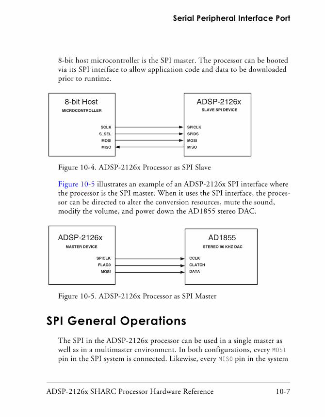
ADSP-2126x SHARC Processor Hardware Reference 10-7
Serial Peripheral Interface Port
8-bit host microcontroller is the SPI master. The processor can be booted via its SPI interface to allow application code and data to be downloaded prior to runtime.
Figure 10-5 illustrates an example of an ADSP-2126x SPI interface where the processor is the SPI master. When it uses the SPI interface, the proces-sor can be directed to alter the conversion resources, mute the sound, modify the volume, and power down the AD1855 stereo DAC.
SPI General OperationsThe SPI in the ADSP-2126x processor can be used in a single master as well as in a multimaster environment. In both configurations, every MOSI pin in the SPI system is connected. Likewise, every MISO pin in the system
Figure 10-4. ADSP-2126x Processor as SPI Slave
Figure 10-5. ADSP-2126x Processor as SPI Master
MICROCONTROLLER
SCLK
S_SEL
MOSI
ADSP-2126xSLAVE SPI DEVICE
SPICLK
SPIDS
MOSI
8-bit Host
MISO MISO
ADSP-2126xMASTER DEVICE
SPICLK
FLAG0
MOSI
AD1855STEREO 96 KHZ DAC
CCLK
CLATCH
DATA
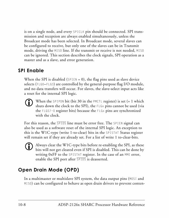
10-8 ADSP-2126x SHARC Processor Hardware Reference
is on a single node, and every SPICLK pin should be connected. SPI trans-mission and reception are always enabled simultaneously, unless the Broadcast mode has been selected. In Broadcast mode, several slaves can be configured to receive, but only one of the slaves can be in Transmit mode, driving the MISO line. If the transmit or receive is not needed, MISO can be ignored. This section describes the clock signals, SPI operation as a master and as a slave, and error generation.
SPI EnableWhen the SPI is disabled (SPIEN = 0), the flag pins used as slave device selects (FLG0–FLG3) are controlled by the general-purpose flag I/O module, and no data transfers will occur. For slaves, the slave-select input acts like a reset for the internal SPI logic.
When the SPIPDN bit (bit 30 in the PMCTL register) is set (= 1 which shuts down the clock to the SPI), the FLGx pins cannot be used (via the FLGS7–0 register bits) because the FLGx pins are synchronized with the clock.
For this reason, the SPIDS line must be error free. The SPIEN signal can also be used as a software reset of the internal SPI logic. An exception to this is the W1C-type (write 1-to-clear) bits in the SPISTAT Status register will remain set if they are already set. For a list of write 1 to-clear-bits.
Always clear the W1C-type bits before re-enabling the SPI, as these bits will not get cleared even if SPI is disabled. This can be done by writing 0xFF to the SPISTAT register. In the case of an MME error, enable the SPI port after SPIDS is deasserted.
Open Drain Mode (OPD)In a multimaster or multislave SPI system, the data output pins (MOSI and MISO) can be configured to behave as open drain drivers to prevent conten-

ADSP-2126x SHARC Processor Hardware Reference 10-9
Serial Peripheral Interface Port
tion and possible damage to pin drivers. An external pull-up resistor is required on both the MOSI and MISO pins when this option is selected.
When the OPD is set and the SPI port is configured as a master, the MOSI pin is three-stated when the data driven out on MOSI is logic-high. The MOSI pin is not three-stated when the driven data is logic-low. A zero is driven on the MOSI pin in this case. Similarly, when OPD is set and the SPI port is configured as a slave, the MISO pin is three-stated if the data driven out on MISO is logic-high.
Master Mode OperationWhen the SPI is configured as core master (and DMA mode is not selected), the SPI port should be configured and transfers started using the following steps:
1. When CPHASE is set to 0, the slave selects are automatically con-trolled by the SPI port. Otherwise [CPHASE = 1] the slave selects are controlled by the core, and user software controls the pins through the SPIFLGx bits. Before enabling the SPI port, programs should specify which slave-select signal to use by writing to the SPIFLG reg-ister, setting one or more of the SPI Flag Select bits (DSxEN).
2. Write to the SPICTL and SPIBAUD registers, enabling the device as a master and configuring the SPI system by specifying the appropri-ate word length, transfer format, baud rate, and other necessary information.
3. If CPHASE = 1 (user-controlled slave-select signals), activate the desired slaves by clearing one or more of the SPI flag bits (SPIFLG) in the SPIFLG register.
4. Initiate the SPI transfer. The trigger mechanism for starting the transfer is dependant upon the TIMOD bits in the SPICTL register. See Table 10-1 on page 10-16 for details.

10-10 ADSP-2126x SHARC Processor Hardware Reference
5. The SPI generates the programmed clock pulses on SPICLK and simultaneously shifts data out of MOSI and shifts data in from MISO. Before starting to shift, the Transmit Shift register is loaded with the contents of the TXSPI register. At the end of the transfer, the contents of the Receive Shift register are loaded into RXSPI.
6. With each new transfer initiate command, the SPI continues to send and receive words, according to the SPI Transfer mode (TIMOD in SPICTL). See Table 10-1 on page 10-16 for more details.
Slave Mode OperationWhen a device is enabled as a slave, the start of a transfer is triggered by a transition of the SPIDS Select signal to the active state (LOW) or by the first active edge of the clock (SPICLK), depending on the state of CPHASE.
The following steps illustrate SPI operation in the slave mode:
1. Write to the SPICTL register to make the mode of the serial link the same as the mode that is setup in the SPI master.
2. To prepare for the data transfer, write the data to be transmitted into the TXSPI register.
3. Once the SPIDS signal’s falling edge is detected, the slave starts sending and receiving data on active SPICLK edges.
4. The reception or transmission continues until SPIDS is released or until the slave has received the proper number of clock cycles.
5. The slave device continues to receive or transmit with each new falling-edge transition on SPIDS or active SPICLK clock edge.

ADSP-2126x SHARC Processor Hardware Reference 10-11
Serial Peripheral Interface Port
If the transmit buffer remains empty, or the receive buffer remains full, the devices operate according to the states of the SENDZ and GM bits in the SPICTL register.
• If SENDZ = 1 and the transmit buffer is empty, the device repeatedly transmits zero’s on the MISO pin.
• If SENDZ = 0 and the transmit buffer is empty, it repeatedly trans-mits the last word it transmitted before the transmit buffer became empty.
• If GM = 1 and the receive buffer is full, the device continues to receive new data from the MOSI pin, overwriting the older data in the RXSPI buffer.
• If GM = 0 and the receive buffer is full, the incoming data is dis-carded, and the RXSPI register is not updated.
Multimaster ConditionsA Multimaster mode is implemented to allow an SPI system to transition mastership from one SPI device to another. In a multidevice SPI configu-ration, several SPI ports are connected and any one of them can become a master at a given time, but only one master is allowed at any one time.
If a processor is a slave and wishes to become the SPI master, it asserts the SPIDS pin for the processor that is currently master and then drives the SPICLK signal. Once it receives the SPIDS signal, the device that was master is immediately reconfigured as a slave. In order to safely transition from one master to the other the SPI port features the use of open drain outputs for the data pad drivers in order to avoid data contention.
More information on this topic is described in “Mode Fault Error (MME)” on page 10-40.

SPI Data Transfer Operations
10-12 ADSP-2126x SHARC Processor Hardware Reference
SPI Data Transfer OperationsThe following sections provide information on the two methods the ADSP-2126x uses to transfer data; through the core or through DMA.
Core Transmit and Receive OperationsFor core-driven SPI transfers, the software has to read from or write to the RXSPI and TXSPI registers to control the transfer. It is important to check the buffer status before reading from or writing to these registers because the core does not hang when it attempts to read from an empty buffer or write to a full buffer. When the core writes to a full buffer, the data that is in that buffer is overwritten and the SPI begins transmitting the new data. Invalid data is obtained when the core reads from an empty buffer.
For a master, when the transmit buffer becomes empty, or the receive buffer becomes full, the SPI device stalls the SPI clock until it reads all the data from the receive buffer or it detects that the transmit buffer contains a piece of data.
• For a master configured with TIMOD = 01: When the transmit buffer becomes empty, the SPI device stalls the SPI clock until a piece of data is written to the transmit buffer.
• For a master configured with TIMOD = 00: When the receive buffer becomes full the SPI device stalls the SPI clock until all of the data is read from the receive buffer.
SPI DMAThe SPI has a single DMA channel associated with it that can be config-ured to support either an SPI transmit or a receive channel, but not both simultaneously. In addition to the TXSPI and RXSPI data buffers, there is a four-word deep DMA FIFO the SPI port uses to improve throughput.

ADSP-2126x SHARC Processor Hardware Reference 10-13
Serial Peripheral Interface Port
The SPI port supports both Master mode and Slave mode DMA. The fol-lowing sections describe Slave and Master mode DMA operation, DMA chaining, switching between transmit and receive DMA operations, and processing DMA interrupt errors.
Do not write to the TXSPI register during an active SPI transmit DMA operation because DMA data will be overwritten. However, writes to the TXSPI register during an active SPI receive DMA oper-ation are permitted. The RXS register is cleared when the RXSPI register is read. Reads from the RXSPI register are allowed at any time during transmit DMA. Interrupts are generated based on DMA events and are configured in the SPIDMAC register.
Similarly, do not read from the RXSPI register during active SPI DMA receive operations.
In order for a transmit DMA operation to begin, the transmit buffer must initially be empty (TXS = 0). While this is normally the case, this means that the TXSPI register should not be used for any purpose other than SPI transfers. For example, the TXSPI register should not be used as a scratch register for temporary data storage. Writing to the TXSPI register via the software sets the TXS bit.
When the SPI DMA engine is configured for transmitting:
1. The receive interface cannot generate an interrupt, but the status can be polled.
2. The four-deep FIFO is not available in the receive path.
Similarly, when the SPI DMA engine is configured for receiving,
1. The transmit interface cannot generate an interrupt, but the status can be polled.
2. The four-deep FIFO is not available in the transmit path.

SPI Data Transfer Operations
10-14 ADSP-2126x SHARC Processor Hardware Reference
Master Mode DMA Operation
To configure the SPI port for Master mode DMA transfers:
1. Specify which FLG pin(s) to use as the slave-select signal(s) by set-ting one or more of the SPI Flag (SPIFLG register) Select bits (DSxEN bits 3–0).
2. Enable the device as a master and configure the SPI system by selecting the appropriate word length, transfer format, baud rate, and so on in the SPIBAUD and SPICTL registers. The TIMOD field (bits 1–0) in the SPICTL register is configured to select transmit or receive with DMA mode (TIMOD = 10).
3. Activate the desired slaves by clearing one or more of the SPI flag bits (SPIFLGx) of SPIFLG if CPHASE = 1.
4. For a single DMA, define the parameters of the DMA transfer by writing to the IISPI, IMSPI, and CSPI registers. For DMA chaining, write the chain pointer address to the CPSPI register. The CPSPI register is a 20-bit read-write register that can contain address information.
5. Write to the SPI DMA configuration register, (SPIDMAC), to specify the DMA direction (SPIRCV, bit 1) and to enable the SPI DMA engine (SPIDEN, bit 0). If DMA chaining is desired, set (= 1) the SPICHEN bit (bit 4) in the SPIDMAC register.
To avoid data corruption, enable the SPI port before enabling DMA.
If flags are used as slave selects, programs should activate the flags by clear-ing the flag after SPICTL and SPIBAUD are configured, but before enabling the DMA. When CPHASE = 0, and a program is using DMA, the program must use automatic flags using SPIFLGx.

ADSP-2126x SHARC Processor Hardware Reference 10-15
Serial Peripheral Interface Port
When enabled as a master, the DMA engine transmits or receives data as follows:
1. If the SPI system is configured for transmitting, the DMA engine reads data from memory into the SPI DMA FIFO. Data from the DMA FIFO is loaded into the TXSPI register and then into the Transmit Shift register. This initiates the transfer on the SPI port.
2. If configured to receive, data from RXSPI is automatically loaded into the SPI DMA FIFO, the DMA engine reads data from the SPI DMA FIFO and writes to memory. Finally, the SPI initiates the receive transfer.
3. The SPI generates the programmed signal pulses on SPICLK and simultaneously shifts data out of MOSI and shifts data in from MISO.
4. The SPI continues sending or receiving words until the SPI DMA word count register transitions from 1 to 0.
If the DMA engine is unable to keep up with the transmit stream during a transmit operation because the IOP requires the IOD (I/O data) bus to service another DMA channel (or for another reason), the SPICLK stalls until data is written into the TXSPI register. All aspects of SPI receive oper-ation should be ignored. The data in the RXSPI register is not intended to be used, and the RXS (bits 28–27 and 31–30 in the SPCTLx register) and SPISTAT bits (bits 26 and 29) should be ignored. The ROVF overrun condi-tion cannot generate an error interrupt in this mode.
If the DMA engine cannot keep up with the receive data stream during receive operations, then SPICLK stalls until data is read from RXSPI. While performing a receive DMA, the processor core assumes the transmit buffer is empty. If SENDZ = 1, the device repeatedly transmits 0’s on the MOSI pin.

SPI Data Transfer Operations
10-16 ADSP-2126x SHARC Processor Hardware Reference
If SENDZ = 0, it repeatedly transmits the contents of the TXSPI register. The TUNF underrun condition cannot generate an error interrupt in this mode.
For receive DMA in master mode the SPICLK stops only when the FIFO and RXSPI buffer is full (even if the DMA count is zero). Therefore, SPICLK runs for an additional five word transfers filling junk data in the FIFO and the RXSPI buffer. This data must be cleared before a new DMA is initiated.
A master SPI DMA sequence may involve back-to-back transmission and/or reception of multiple DMA transfers. The SPI controller supports such a sequence with minimal processor core interaction.
Master Transfer Preparation
When the processor is enabled as a master, the initiation of a transfer is defined by the two bit fields (bits 1–0) of TIMOD in the SPICTL register. Based on these two bits and the status of the interface, a new transfer is started upon either a read of the RXSPI register or a write to the TXSPI reg-ister. This is summarized in Table 10-1.
Table 10-1. Transfer Initiation
TIMOD Function Transfer Initiated Upon Action, Interrupt
00 Transmit and Receive
Initiate new single word transfer upon read of RXSPI and previous trans-fer completed.
The SPI interrupt is latched in every core clock cycle in which the RXSPI buffer has a word in it.Emptying the RXSPI buffer or dis-abling the SPI port at the same time (SPIEN = 0) stops the interrupt latch.
01 Transmit and Receive
Initiate new single word transfer upon write to TXSPI and previous trans-fer completed.
The SPI interrupt is latched in every core clock cycle in which the TXSPI buffer is empty.Writing to the TXSPI buffer or dis-abling the SPI port at the same time (SPIEN = 0) stops the interrupt latch.

ADSP-2126x SHARC Processor Hardware Reference 10-17
Serial Peripheral Interface Port
Slave Mode DMA Operation
A Slave mode DMA transfer occurs when the SPI port is enabled and con-figured in Slave mode, and DMA is enabled. When the SPIDS signal transitions to the active-low state or when the first active edge of SPICLK is detected, it triggers the start of a transfer.
To configure for Slave mode DMA:
1. Write to the SPICTL register to make the mode of the serial link the same as the mode that is set up in the SPI master. Configure the TIMOD field to select transmit or receive DMA mode (TIMOD = 10).
2. Define a DMA receive (or transmit) transfer by writing to the IISPI, IMSPI, and CSPI registers. For DMA chaining, write to the chain pointer address of the CPSPI register.
10 Transmit or Receive with DMA
Initiate new multiword transfer upon write to DMA Enable bit. Individ-ual word transfers begin with either a DMA write to TXSPI or a DMA read of RXSPI depending on the direction of the trans-fer as specified by the SPIRCV bit.
If chaining is disabled, the SPI inter-rupt is latched in the cycle when the DMA count decrements from 1 to 0. If chaining is enabled, interrupt func-tion is based on the PCI bit in the CP register. If PCI = 0, the SPI interrupt is latched at the end of the DMA sequence. If PCI = 1, then the SPI interrupt is latched after each DMA in the sequence. For more informa-tion, see “DMA Transfer Direction” on page 7-21.
11 Reserved
Table 10-1. Transfer Initiation (Cont’d)
TIMOD Function Transfer Initiated Upon Action, Interrupt

SPI Data Transfer Operations
10-18 ADSP-2126x SHARC Processor Hardware Reference
3. Write to the SPIDMAC register to enable the SPI DMA engine and configure:
• A receive access (SPIRCV = 1) or
• A transmit access (SPIRCV = 0)
If DMA chaining is desired, set the SPICHEN bit in the SPIDMAC register.
Enable the SPI port before enabling DMA to avoid data corruption.
Slave Transfer Preparation
When enabled as a slave, the device prepares for a new transfer according to the function and actions described in Table 10-1.
The following steps illustrate the SPI receive or transmit DMA sequence in an SPI slave in response to a master command:
1. Once the slave-select input is active, the processor starts receiving and transmitting data on active SPICLK edges. The data for one channel (TX or RX) is automatically transferred to/from memory by the IOP. The function of the other channel is dependant on the GM and SENDZ bits in the SPICTL register.
2. Reception or transmission continues until the SPI DMA word count register transitions from 1 to 0.
3. A number of conditions can occur while the processor is configured for Slave mode:
• If the DMA engine cannot keep up with the receive data stream during receive operations, the receive buffer operates according to the state of the GM bit in the SPICTL register.

ADSP-2126x SHARC Processor Hardware Reference 10-19
Serial Peripheral Interface Port
• If GM = 0 and the DMA buffer is full, the incoming data is discarded, and the RXSPI register is not updated. While per-forming a receive DMA, the transmit buffer is assumed to be empty. If SENDZ = 1, the device repeatedly transmits zero’s on the MOSI pin. If SENDZ = 0, it repeatedly transmits the contents of the TXSPI register.
• If GM = 1 and the DMA buffer is full, the device continues to receive new data from the MISO pin, overwriting the older data in the DMA buffer.
• If the DMA engine cannot keep up with the transmit data stream during a transmit operation because another DMA engine has been granted the bus (or for another reason), the transmit port operates according to the state of the SENDZ bit in the SPICTL register.
If SENDZ = 1 and the DMA buffer is empty, the device repeatedly transmits zero’s on the MOSI pin. If SENDZ = 0 and the DMA buffer is empty, it repeatedly transmits the last word it transmitted before the DMA buffer became empty. All aspects of SPI receive operation should be ignored. The data in the RXSPI register is not intended to be used, and the RXS and ROVF bits should be ignored. The ROVF overrun con-dition cannot generate an error interrupt in this mode.
While a DMA transfer may be used on one channel (TX or RX), the core, (based on the RXS and TXS status bits), can transfer data in the other direction.
SPI Data Transfer Operations
10-20 ADSP-2126x SHARC Processor Hardware Reference
Changing SPI Configuration
Programs should take the following precautions when changing SPI configurations.
• The SPI configuration must not be changed during a data transfer.
• Change the clock polarity only when no slaves are selected.
• Change the SPI configuration when SPIEN = 0. For example, if operating as a master in a multislave system, and there are slaves that require different data or clock formats, then the master SPI should be disabled, reconfigured, and then re-enabled. However, when an SPI communication link consists of the follow-ing: 1) a single master and a single slave, 2) CPHASE = 1, and 3) the slave’s slave select input is tied low, the program can change the SPI configuration. In this case, the slave is always selected. Data corruption can be avoided by enabling the slave only after config-uring both the master and slave devices.
When performing transmit operations with the SPI port, disabling the SPI port prematurely can cause data to be corrupted and or not fully transmit-ted. Before the program disables the SPI port in order to reconfigure it, the status bits should be polled to ensure that all valid data has been com-pletely transferred. For core-driven transfers, data moves from the TXSPI buffer into a shift register. The following bits should be checked before disabling the SPI port:
1. Wait for the TXSPI buffer to empty into the shift register. This is done when the TXS bit, (bit 3) of the SPISTAT register becomes zero.
2. Wait for the SPI Shift register to finish shifting out data This is done when the SPIF bit, (bit 0) of the SPISTAT register becomes one.

ADSP-2126x SHARC Processor Hardware Reference 10-21
Serial Peripheral Interface Port
3. Disable the SPI Port by setting the SPIEN bit, (bit 0) in the SPICTL register, to zero.
When performing transmit DMA transfers, data moves through a four deep SPI DMA FIFO, then into the TXSPI buffer, and finally into the shift register. DMA interrupts are latched when the I/O processor moves the last word from memory to the peripheral. For the SPI, this means that the SPI “DMA complete” interrupt is latched when there are still six words left to be fully transmitted (four in the FIFO, one in the TXSPI buffer, and one being shifted out of the Shift register). To disable the SPI port after a DMA transmit operation, use these steps:
1. Wait for DMA FIFO to empty. This is done when the SPISx bits (bits 13–12) in the SPIDMAC register become zero.
2. Wait for the TXSPI register to empty. This is done when the TXS bit (bit 3) in the SPISTAT register becomes zero.
3. Wait for the SPI Shift register to finish transferring the last word. This is done when the SPIF bit, (bit 0) of the SPISTAT register, becomes one.
4. Disable the SPI Port by setting the SPIEN bit, (bit 0) of the SPICTL register, to zero.
Switching From Transmit To Receive DMA
The following sequence details the steps for switching from transmit to receive DMA.
With disabling the SPI:
1. Write 0x00 to the SPICTL register to disable SPI. Disabling the SPI also clears the RXSPI/TXSPI registers and the buffer status.
2. Disable DMA by writing 0x00 to the SPIDMAC register.

SPI Data Transfer Operations
10-22 ADSP-2126x SHARC Processor Hardware Reference
3. Clear all errors by writing to the W1C-type bits in the SPISTAT reg-ister. This ensures that no interrupts occur due to errors from a previous DMA operation.
4. Reconfigure the SPICTL register and enable the SPI port.
5. Configure DMA by writing to the DMA parameter registers and enable DMA.
Without disabling the SPI:
1. Clear RXSPI/TXSPI without disabling SPI. This can be done by ORing 0xc0000 with the present value in the SPICTL register. For example programs can use the RXFLSH and TXFLSH bits to clear TXSPI/RXSPI.
2. Disable DMA by writing 0x00 to the SPIDMAC register.
3. Clear all errors by writing to the MME bit (bit 1) in the SPISTAT reg-ister. This ensures that no interrupts occur due to errors from a previous DMA operation.
4. Reconfigure the SPICTL register to clear the TXSPI/RXSPI register values.
5. Configure DMA by writing to the DMA parameter registers and enabling DMA.
Switching From Receive to Transmit DMA
Use the following sequence to switch from receive to transmit DMA. Note that TXSPI and RXSPI are registers but they may not contain any bits, only address information.

ADSP-2126x SHARC Processor Hardware Reference 10-23
Serial Peripheral Interface Port
With disabling of the SPI:
1. Write 0x00 to the SPICTL register to disable SPI. Disabling SPI also clears the RXSPI/TXSPI register contents and the buffer status.
2. Disable DMA and clear the DMA FIFO by writing 0x80 to the SPIDMAC register. This ensures that any data from a previous DMA operation is cleared because the SPICLK signal runs for five more word transfers even after the DMA count falls to zero in receive DMA.
3. Clear all errors by writing to the SPISTAT register. This ensures that no interrupts occur due to errors from a previous DMA operation.
4. Reconfigure the SPICTL register and enable SPI.
5. Configure DMA by writing to the DMA parameter registers and the SPIDMAC register.
Without disabling the SPI:
1. Clear RXSPI/TXSPI without disabling the SPI. This can be done by ORing 0xc0000 with the present value in the SPICTL register. Use the RXFLSH (bit 19) and TXFLSH (bit 18 in the SPICTL register) bits to clear the RXSPI/TXSPI registers.
2. Disable DMA and clear the FIFO. For example, write 0x80 to the SPIDMAC register. This ensures that any data from a previous DMA operation clears because the SPICLK runs for five more word trans-fers even after the DMA count is zero in receive DMA.
3. Clear all errors by writing to the W1C-type bits in the SPISTAT reg-ister. This ensures that no interrupts occur due to errors from a previous DMA operation.

SPI Data Transfer Operations
10-24 ADSP-2126x SHARC Processor Hardware Reference
4. Reconfigure the SPICTL register to clear the TXSPI/RXSPI registers.
5. Configure DMA by writing to the DMA parameter registers and the SPIDMAC register using the SPIDEN bit (bit 0). These registers are described in Table 7-4 on page 7-25.
DMA Error Interrupts
The SPIUNF and SPIOVF bits of the SPIDMAC register indicate transmission errors during a DMA operation in Slave mode. When one of the bits is set, an SPI interrupt occurs. The following sequence details the steps to respond to this interrupt.
With disabling the SPI:
1. Disable the SPI port by writing 0x00 to the SPICTL register.
2. Disable DMA and clear the FIFO. For example, write 0x80 to the SPIDMAC register. This ensures that any data from a previous DMA operation clears before configuring a new DMA operation.
3. Clear all errors by writing to the W1C-type bits (see ) in the SPI-STAT register. This ensures that the error bits SPIOVF and SPIUNF (in the SPIDMAC register) clear when a new DMA is configured.
4. Reconfigure the SPICTL register and enable SPI using the SPIEN bit.
5. Configure DMA by writing to the DMA parameter registers and the SPIDMAC register.

ADSP-2126x SHARC Processor Hardware Reference 10-25
Serial Peripheral Interface Port
Without disabling the SPI:
1. Disable DMA and clear the FIFO. For example, write 0x80 to the SPIDMAC register. This ensures that any data from a previous DMA operation clears before configuring a new DMA operation.
2. Clear RXSPI/TXSPI without disabling SPI. This can be done by ORing 0xc0000 with the present value in the SPICTL register. Use the RXFLSH and TXFLSH bits to clear the RXSPI/TXSPI registers.
3. Clear all errors by writing to the W1C-type bits in the SPISTAT register. This ensures that error bits SPIOVF and SPIUNF in the SPIDMAC register are cleared when a new DMA is configured.
4. Reconfigure SPICTL to clear the RXSPI/TXSPI register bits.
5. Configure DMA by writing to the DMA parameter registers and the SPIDMAC register.
DMA Chaining
DMA chaining is enabled when the SPICHEN bit is set to 1 in the SPIDMAC register. In this mode, the DMA registers are loaded using a DMA transfer from a predefined Transfer Control Block (TCB). When this load occurs, it causes the Chaining Status bit (SPICHS) to be set. Once the chain pointer load completes, the SPICHS bit is cleared. Upon completion of the transfer block load, the normal DMA transfer is initiated. Table 10-2 describes the order of loading. For more information about chaining, refer to “Chaining DMA Processes” on page 7-10.
Table 10-2. DMA Chaining Sequence
Address Register Description
CPSPI DMA Start Address Address in Memory
CPSPI – 1 DMA Address Modifier Address increment

SPI Transfer Formats
10-26 ADSP-2126x SHARC Processor Hardware Reference
SPI Transfer FormatsThe ADSP-2126x SPI supports four different combinations of serial clock phases and polarity. The application code can select any of these combina-tions using the CLKPL and CPHASE bits in the SPICTL register.
Figure 10-6 on page 10-27 shows the transfer format when CPHASE = 0 where SPICLK starts toggling in the middle of the data transfer, WL = 0, and MSBF = 1. Figure 10-7 on page 10-28 shows the transfer format when CPHASE = 1. Each diagram shows two waveforms for SPICLK—one for CLKPL = 0 and the other for CLKPL = 1. The diagrams may be interpreted as master or slave timing diagrams since the SPICLK, MISO, and MOSI pins are directly connected between the master and the slave. The MISO signal is the output from the slave (slave transmission), and the MOSI signal is the out-put from the master (master transmission).
The SPICLK signal is generated by the master, and the SPIDS signal repre-sents the slave device select input to the processor from the SPI master. The diagrams represent 8-bit transfers (WL = 0) with MSB first (MSBF = 1). Any combination of the WL and MSBF bits of the SPICTL register is allowed. For example, a 16-bit transfer with the LSB first is one possible configuration.
The clock polarity and the clock phase should be identical for the master device and slave devices involved in the communication link. The transfer format from the master may be changed between transfers to adjust to var-ious requirements of a slave device.
CPSPI – 2 DMA Word Count Number of words to transfer
CPSPI – 3 DMA Next TCB Pointer to address of next TCB
Table 10-2. DMA Chaining Sequence (Cont’d)
Address Register Description

ADSP-2126x SHARC Processor Hardware Reference 10-27
Serial Peripheral Interface Port
When CPHASE = 0, the slave select line, SPIDS, must be inactive (HIGH) between each word in the transfer. When CPHASE = 1, SPIDS may either remain active (LOW) between successive transfers or be inactive (HIGH).
Figure 10-7 shows the SPI transfer protocol for CPHASE = 1. Note that SPICLK starts toggling at the beginning of the data transfer, WL = 0, and MSBF = 1.
Figure 10-6. SPI Transfer Protocol for CPHASE = 0
1CLOCK CYCLENUMBER
SPICLKCLKPL = 0
MOSIFROM MASTER
MISOFROM SLAVE
SPIDSFROM MASTER
SPICLKCLKPL = 1
2 3 4 5 6 7 8
* 6
6 5 4 3
5 4 3 2 1 LSB *
2 1 LSB *
MSB
MSB
* = UNDEFINED

SPI Transfer Formats
10-28 ADSP-2126x SHARC Processor Hardware Reference
Beginning and Ending an SPI TransferAn SPI transfer’s defined start and end depend on the following: whether the device is configured as a master or a slave, whether the CPHASE mode is selected, and whether the transfer initiation mode is (TIMOD) selected. For a master SPI with CPHASE = 0, a transfer starts when either the TXSPI regis-ter is written or the RXSPI register is read, depending on the TIMOD selection. At the start of the transfer, the enabled slave-select outputs are driven active (LOW). However, the SPICLK starts toggling after a delay equal to one-half the SPICLK period. For a slave with CPHASE = 0, the transfer starts as soon as the SPIDS input transitions to low.
For CPHASE = 1, a transfer starts with the first active edge of SPICLK for both slave and master devices. For a master device, a transfer is considered complete after it sends and simultaneously receives the last data bit. A transfer for a slave device is complete after the last sampling edge of SPICLK.
Figure 10-7. SPI Transfer Protocol for CPHASE = 1
1CLOCK CYCLENUMBER
SPICLKCLKPL=0
MOSIFROM MASTER
MISOFROM SLAVE
SPIDSTO SLAVE
SPICLKCLKPL=1
2 3 4 5 6 7 8
* 6
6 5 4 3
5 4 3 2 1 LSB *
2 1 LSB
MSB
MSB
* = UNDEF INED
*

ADSP-2126x SHARC Processor Hardware Reference 10-29
Serial Peripheral Interface Port
The RXS bit defines when the receive buffer can be read; the TXS bit defines when the transmit buffer can be filled. The end of a single word transfer occurs when the RXS bit is set. This indicates that a new word has just been received and latched into the receive buffer, RXSPI. The RXS bit is set shortly after the last sampling edge of SPICLK. The latency is typically a few core clock cycles and is independent of CPHASE, TIMOD, and the baud rate. If configured to generate an interrupt when RXSPI is full (TIMOD = 00), the interrupt becomes active one core clock cycle after RXS is set. When not relying on this interrupt, the end of a transfer can be detected by polling the RXS bit.
To maintain software compatibility with other SPI devices, the SPI Trans-fer Finished bit (SPIF) is also available for polling. This bit may have slightly different behavior from that of other commercially available devices. For a slave device, SPIF is set at the same time as RXS; for a master device, SPIF is set one-half of the SPICLK period after the last SPICLK edge, regardless of CPHASE or CLKPL.
The baud rate determines when the SPIF bit is set. In general, SPIF is set after RXS, but at the lowest baud rate settings (SPIBAUD<4). The SPIF bit is set before the RXS bit is set, and consequently before new data has been latched into the RXSPI buffer. For SPIBAUD = 2 or SPIBAUD = 3, the proces-sor must wait for the RXS bit to be set (after SPIF is set) before reading the RXSPI buffer. For larger SPIBAUD settings (SPIBAUD > 4), RXS is set before SPIF is set.
SPI Word LengthsThe processor’s SPI port can transmit and receive the word widths described in the following sections.

SPI Word Lengths
10-30 ADSP-2126x SHARC Processor Hardware Reference
8-Bit Word LengthsEight-bit word lengths can be used when transmitting or receiving. When transmitting, the SPI port sends out only the lower eight bits of the word written to the SPI buffer.
For example, if the processor executes the instructions below, the SPI port transmits 0x78.
r0 = 0x12345678
dm(TXSPI) = r0;
When receiving, the SPI port packs the 8-bit word to the lower 32 bits of the RXSPI buffer while the upper bits in the registers are zeros.
For example, if an SPI host sends the processor the 32-bit word 0x12345678, the processor receives the following words:
0x00000078 //first word
0x00000056 //second word
0x00000034 //third word
0x00000012 //forth word
This code works only if the MSBF bit is zero in both the transmitter and receiver, and the SPICLK frequency is small. If MSBF = 1 in the transmitter and receiver, and SPICLK has a small frequency, the received words follow the order 0x12, 0x34, 0x56, 0x78.
16-Bit Word LengthsSixteen-bit word lengths can be used when transmitting or receiving. When transmitting, the SPI port sends out only the lower 16 bits of the word written to the SPI buffer.

ADSP-2126x SHARC Processor Hardware Reference 10-31
Serial Peripheral Interface Port
For example, if the processor executes the following instructions, the SPI port transmits 0x5678.
r0 = 0x12345678
dm(TXSPI) = r0;
When receiving, the SPI port packs the 16-bit word to the lower 32 bits of the RXSPI buffer while the upper bits in the register are zeros.
For example, if an SPI host sends the processor the 32-bit word 0x12345678, the processor receives the following words:
0x00005678 //first word
0x00001234 //second word
32-Bit Word LengthsThirty-two bit word lengths can be used when transmitting or receiving. No packing of the RXSPI or TXSPI registers is necessary as the entire 32-bit register is used for the data word.
Packing In order to communicate with 8-bit SPI devices and store 8-bit words in internal memory, a packed transfer feature is built into the SPI port. Pack-ing is enabled through the PACKEN bit in the SPICTL register. The SPI is unpacks data when it transmits and packs data when it receives. When packing is enabled, two 8-bit words are packed into one 32-bit word. When the SPI port is transmitting, two eight-bit words are packed into one 32-bit word. When receiving, words are unpacked from one 32-bit word into two eight-bit words.

SPI Interrupts
10-32 ADSP-2126x SHARC Processor Hardware Reference
Transmitter packing example:
The value 0xXXLMXXJK (where XX is any random value and JK and LM are the data words to be transmitted out of the SPI port) is written to the TXSPI register. The processor transmits 0xJK first and then transmits 0xLM.
Receiver packing example:
The receiver unpacks the value and two words are received, 0xJK and then 0xLM. They appear in the RXSPI register as:
0x00LM00JK => if SGN is configured to 0 0xFFLMFFJK => if SGN is configured to 1 and L, J > 7.
SPI InterruptsThe SPI port can generate an interrupt in five different situations. During core-driven transfers, an SPI interrupt is triggered in these instances:
1. When the TXSPI buffer has the capacity to accept another word from the core
2. When the RXSPI buffer contains a valid word to be retrieved by the core
The TIMOD (Transfer Initiation and Interrupt) register determines whether the interrupt is based on the TXSPI or RXSPI buffer status. For more infor-mation, refer to the TIMOD bit descriptions in the SPICTL register in Table on page A-94.

ADSP-2126x SHARC Processor Hardware Reference 10-33
Serial Peripheral Interface Port
During IOP-driven transfers (DMA), an SPI interrupt is triggered in these instances:
1. When a single DMA transfer completes
2. When a number of DMA sequences (if DMA chaining is enabled) completes
3. When a DMA error has occurred
Again, the TIMOD register must be initialized properly to enable DMA interrupts.
All of these interrupts are serviced using the high priority (SPIHI) or low priority (SPILI) SPI interrupt. Whenever an SPI interrupt occurs (regard-less of the cause), both SPILI and SPIHI are latched. Programs specify the SPI interrupt priority by masking (disabling) one of the interrupts. To ser-vice the SPI port using the high priority interrupt, unmask (set = 1) the SPIHI bit (bit 12) in the IMASK register. To service the SPI port using the low priority interrupt, unmask (set = 1) the SPILIMSK bit (bit 19) in the LIRPTL register. For a list of these bits, see Table 7-1 on page 7-5.
To globally enable interrupts set (= 1), the IRPTEN bit in the MODE1 register. When using DMA transfers, programs must also specify whether to gener-ate interrupts based on transfer or error status. For DMA transfer status based interrupts, set the INTEN bit in the SPIDMAC register; otherwise, set the INTERR bit to trigger the interrupt if one of the error conditions is trig-gered during the transmission—multimaster error (MME), transmit buffer underflow (TUNF – only if SPIRCV = 0), or receive buffer overflow (ROVF – only if SPIRCV = 1). During core-driven transfers, the TUNF and ROVF error conditions do not generate interrupts.
When DMA is disabled, the processor core may read from the RXSPI regis-ter or write to the TXSPI data buffer. The RXSPI and TXSPI buffers are memory-mapped IOP registers. A maskable interrupt is generated when

SPI Registers
10-34 ADSP-2126x SHARC Processor Hardware Reference
the receive buffer is not empty or the transmit buffer is not full. The TUNF and ROVF error conditions do not generate interrupts in these modes.
• See the “Program Sequencer Registers” on page A-22 for IRPTL and LIRPTL register bit descriptions.
• See “SPI DMA Configuration (SPIDMAC) Register” on page A-101 for SPIDMAC register bit descriptions.
SPI RegistersThe SPI peripheral in the ADSP-2126x SHARC processor includes several memory-mapped registers, some of which are accessible by the IOP. Four registers contain control and status information—SPIBAUD, SPICTL, SPIFLG, and SPISTAT. Two registers are used for buffering receive and transmit data—RXSPI and TXSPI. Five registers are related to DMA func-tionality—SPIDMAC, IISPI, IMSPI, CSPI and CPSPI. Additionally, the four-deep SPI DMA FIFO and the SPI Transmit and Receive Shift regis-ters, TXSR and RXSR, are not accessible.
Control and Status RegistersThe following registers are used to control certain functions of the SPI or to provide SPI status information.
SPI Baud Setup Register (SPIBAUD)
The SPI Baud Rate register (SPIBAUD) is used to set the bit transfer rate for a master device. When configured as a slave, the value written to this reg-ister is ignored. The serial clock frequency is determined by the following formula:
SPI Baud Rate = Core Clock Rate
(4)x(BAUDR)

ADSP-2126x SHARC Processor Hardware Reference 10-35
Serial Peripheral Interface Port
Writing a value of zero to the register disables the serial clock. Therefore, the maximum serial clock rate is one-fourth the core clock rate (CCLK).
Table 10-3 provides the bit descriptions for the SPIBAUD register.
Table 10-4 lists several possible baud rate values for the SPIBAUD register.
Table 10-3. SPIBAUD Register Bits
Bit(s) Name Function Default
0 Reserved
15:1 BAUDR Baud Rate enables the SPICLK baud rate per the following equation:SPI Baud Rate = Core clock (CCLK) divided by (4* BAUDR)
0
31:16 Reserved
Table 10-4. SPI Master Baud Rate Example
BAUDR Decimal Value SPI Clock Divide Factor Baud Rate for CCLK @ 200 MHz
0 N/A N/A
1 4 50 MHz
2 8 25 MHz
3 12 16.67 MHz
4 16 12.5 MHz
5 20 10.0 MHz
and up to 32,767 (0x7FFF)1
1 BAUDR decimal values of 6 to 32,766 are also possible.
131,068 1.526 kHz

SPI Registers
10-36 ADSP-2126x SHARC Processor Hardware Reference
Use of DSxEN Bits in SPIFLG for Multiple Slave SPI Systems
The DSxEN bits in the SPIFLG register are used in a multiple slave SPI envi-ronment. For example, if there are five SPI devices in the system with an ADSP-2126x master, then the master ADSP-2126x processor can support the SPI mode transactions across all four other devices. This configuration requires that only one ADSP-2126x be a master. For example, assume that SPI0 is the master. The four flag pins on the ADSP-2126x master can be connected to each of the slave SPI device’s SPIDS pins. In this configura-tion, the DSxEN bits in the SPIFLG register can be used in three ways.
In cases 1 and 2, the processor acts as the master, and the four SPI micro-controllers/peripherals act as slaves. In this configuration, the ADSP-2126x processor can:
1. Transmit to all four SPI devices at the same time in Broadcast mode. Here, all the DSxEN bits are set.
2. Receive and transmit from one SPI device by enabling only one slave SPI device at a time.
In case 3, all five devices connected via SPI ports can be ADSP-2126x processors.
3. If all the slaves are also ADSP-2126x processors, then the requestor can receive data from only one ADSP-2126x processor (enable this by setting the DMISO bit in the other slave processors) at a time and transmit broadcast data to all four at the same time. This DMISO fea-ture may be available in some other microcontrollers. Therefore, it would be possible to use the DMISO feature with any other SPI device which includes this functionality.
Figure 10-8 shows one ADSP-2126x processor as a master with three ADSP-2126x processors (or other SPI-compatible devices) as slaves.

ADSP-2126x SHARC Processor Hardware Reference 10-37
Serial Peripheral Interface Port
SPI Device Select Input Pin
The behavior of the SPIDS input depends on the configuration of the SPI. If the SPI is a slave, SPIDS acts as the slave-select input. When enabled as a master, SPIDS can serve as an error-detection input for the SPI in a multi-master environment. The ISSEN bit (bit 4) in the SPICTL register enables the SPI master mode feature. When ISSEN=1, the SPIDS input is the mas-ter mode error input; otherwise, SPIDS is ignored. The state of these input pins can be observed in the flag I/O module’s data register.
Buffering and Transmit/Receive RegistersThe TXSPI and RXSPI registers are 32-bit memory-mapped registers that hold SPI data for transmit and receive operations.
Check the buffer status before reading from or writing to these registers because the core does not hang when it attempts to read from an empty buffer or write to a full buffer. When the core writes to a full buffer, the data in that buffer is overwritten and the SPI begins transmitting the new data. Invalid data is obtained when the core reads from an empty buffer.
Figure 10-8. Single Master, Multiple Slave Configuration
MISO
SPICLK
MOSI
SPIDS
SLAVE DEVICE
MISO
SPICLK
MOSI
SPIDS
SLAVE DEVICE
MISO
SPICLK
MOSI
SPIDS
SLAVE DEVICE
MISO
SPICLK
MOSI
SPIDS
MASTERDEVICE
FLAGFLAG
FLAG
VDD

SPI Registers
10-38 ADSP-2126x SHARC Processor Hardware Reference
SPI Transmit Data Buffer Register (TXSPI)
The Transmit Data Buffer register (TXSPI) is a 32-bit read-write (RW)reg-ister. Data is loaded into this register before being transmitted. Just prior to the beginning of a data transfer, the data in TXSPI is loaded into the Transmit Shift Data (SFDR) register. A normal core read of TXSPI can be done at any time and does not interfere with, or initiate, SPI transfers.
With DMA enabled for transmit operations, the IOP loads data into this register. Core writes to TXSPI should not be made to prevent corrupting the DMA data to be transmitted.
With DMA enabled for receive operations, the contents of the TXSPI regis-ter are repeatedly transmitted. A normal core write to TXSPI is permitted in this mode, and this data is transmitted. If the Send Zeroes Control bit (SENDZ) is set, TXSPI resets once the data is transferred from TX to TXSR.
If multiple writes to TXSPI occur while a transfer is already in progress, only the last data written is transmitted. None of the intermediate values written to TXSPI are transmitted. Multiple writes to TXSPI are possible but not recommended. To avoid overwriting data, be sure to poll the TXS bit before writing to TXSPI.
To prevent transmit collision errors, ensure that the program writes to the TXSPI register before the load to the Shift register occurs by writing to TXSPI whenever TXS is cleared. Programs should refrain from writing to TXSPI when TXS is set. For slave mode, data should exist in TXSPI before the first SPI clock edge (or negative edge of device select) occurs.
The TXCOL bit can be set when there is a TUNF condition and there are attempts to write to the TXSPI register. In this case, TXS is not set and the program wants to send new data. To ensure that TXSPI is written into before the next load to a Shift register occurs, write to the TXSPI register as soon as the SPIF bit (bit 0 in the SPISTAT register) goes from one to zero.

ADSP-2126x SHARC Processor Hardware Reference 10-39
Serial Peripheral Interface Port
SPI Receive Data Buffer Register (RXSPI)
The Receive Data Buffer register (RXSPI) is a 32-bit read-only (RO) regis-ter that is accessible by both the software and DMA. At the end of a data transfer, the data in the Receive Shift register (RXSR) loads into the RXSPI register. During a DMA receive operation, the data in the RXSPI register is automatically read by the DMA. A shadow register for the receive data buffer, RXSPI, supports software debugging functions. See “SPI Receive Data Buffer Shadow Register (RXSPI_SHADOW)” on page A-99.
DMA RegistersThe following registers configure and manage SPI DMA functions.
SPI DMA Internal Index Register (IISPI)
This 19-bit register contains the address where the IOP transfers data to or from. Initially, this register holds the first address of the source or desti-nation buffer, and then as the DMA progresses, this register is modified by the value in IMSPI.
SPI DMA Address Modifier Register (IMSPI)
This 16-bit register contains the DMA address modifier. After the IOP transfers each word between memory and the TXSPI/RXSPI register, this value is used to increment the internal index, IISPI

Error Signals and Flags
10-40 ADSP-2126x SHARC Processor Hardware Reference
SPI DMA Word Count Register (CSPI)
This 16-bit register contains the number of DMA words to be transferred. When this register decrements from one to zero, the DMA is complete, and an interrupt may be triggered.
To prematurely end a DMA transfer, software should write the value one to the Count register so that it will decrement to zero. Writing a value of zero causes the count to decrement to a negative number, and this is not advised.
Error Signals and FlagsThis section describes the error signals and flags that determine the cause of transmission errors for an SPI port. The bits MME, TUNF and ROVF are set in the SPISTAT register when a transmission error occurs. Corresponding bits (SPIMME, SPIUNF and SPIOVF) in the SPIDMAC register are set when an error occurs during a DMA transfer. These sticky bits generate an SPI interrupt when any one of them are set.
Mode Fault Error (MME)The MME bit is set in the SPISTAT register when the SPIDS input pin of a device that is enabled as a master is driven low by some other device in the system. This occurs in multimaster systems when another device is also trying to be the master.
To enable this feature, set the ISSEN bit in the SPICTL register. As soon as this error is detected, the following actions are taken.
1. The SPIMS control bit in SPICTL is cleared, configuring the SPI interface as a slave.
2. The SPIEN control bit in SPICTL is cleared, disabling the SPI system.

ADSP-2126x SHARC Processor Hardware Reference 10-41
Serial Peripheral Interface Port
3. The MME status bit in SPISTAT is set.
4. An SPI interrupt is generated.
These four conditions persist until the MME bit is cleared by a write 1-to-clear (W1C-type) software operation. Until the MME bit is cleared, the SPI cannot be re-enabled, even as a slave. Hardware prevents the program from setting either SPIEN or SPIMS while MME is set.
When MME is cleared, the interrupt is deactivated. Before attempting to re-enable the SPI as a master, the state of the SPIDS input pin should be checked to ensure that it is high; otherwise, once SPIEN and SPIMS are set, another mode-fault error condition will immediately occur. The state of the input pin is reflected in the Input Slave Select Status bit (bit 7) in the SPIFLG register.
As a result of SPIEN and SPIMS being cleared, the SPI data and clock pin drivers (MOSI, MISO, and SPICLK) are disabled. However, the slave-select output pins revert to control by the flag I/O module registers. This may cause contention on the slave-select lines if these lines are still being driven by the ADSP-2126x. In order to ensure that the slave-select output drivers are disabled once a MME error occurs, the program must configure these pins as inputs by clearing (= 0) the FLG0O, FLG1O, FLG2O, and FLG3O bits in the FLAGS register prior to configuring the SPI port. See the “Flag Value Register (FLAGS)” on page A-38.
Transmission Error Bit (TUNF)The TUNF bit is set in the SPISTAT register when all of the conditions of transmission are met and there is no new data in TXSPI (TXSPI is empty). In this case, the transmission contents depend on the state of the SENDZ bit in the SPICTL register. The TUNF bit is cleared by a W1C-type software operation.

Programming Model
10-42 ADSP-2126x SHARC Processor Hardware Reference
Reception Error Bit (ROVF)The ROVF flag is set in the SPISTAT register when a new transfer has com-pleted before the previous data could be read from the RXSPI register. This bit indicates that a new word was received while the receive buffer was full. The ROVF flag is cleared by a W1C-type software operation. The state of the GM bit in the SPICTL register determines whether the RXSPI register is updated with the newly received data or whether that new data is discarded.
Transmit Collision Error Bit (TXCOL)The TXCOL flag is set in the SPISTAT register when a write to the TXSPI reg-ister coincides with the load of the Shift register. The write to TXSPI can be via the software or the DMA. This bit indicates that corrupt data may have been loaded into the Shift register and transmitted. In this case, the data in TXSPI may not match what was transmitted. This error can easily be avoided by proper software control. The TXCOL bit is cleared by a W1C-type software operation.
This bit is never set when the SPI is configured as a slave with CPHASE = 0. The collision may occur, but it cannot be detected.
Programming ModelThe section describes which sequences of software steps are required to get the peripheral working successfully.

ADSP-2126x SHARC Processor Hardware Reference 10-43
Serial Peripheral Interface Port
Master Mode Core TransfersWhen the SPI is configured as a master, the SPI ports should be config-ured and transfers started using the following steps:
1. When CPHASE is set to 0 with CPHASE = 1, the slave-selects are auto-matically controlled by the SPI port. When CPHASE = 1, the slave-selects are controlled by the core, and the user software has to control the pins through the SPIFLGx bits. Before enabling the SPI port, programs should specify which of the slave-select signals to use, setting one or more of the required SPI flag select bits (DSxEN) in the SPIFLGx registers.
2. Write to the SPICTLx and SPIBAUDx registers, enabling the device as a master and configuring the SPI system by specifying the appro-priate word length, transfer format, baud rate, and other necessary information.
3. If CPHASE = 1 (user-controlled, slave-select signals), activate the desired slaves by clearing one or more of the SPI flag bits (SPIFLGx) in the SPIFLGx registers.
4. Initiate the SPI transfer. The trigger mechanism for starting the transfer is dependant upon the TIMOD bits in the SPICTLx registers. See Table 10-1 on page 10-16 for details.
5. The SPI generates the programmed clock pulses on SPICLK. The data is shifted out of MOSI and shifted in from MISO simultaneously. Before starting to shift, the transmit shift register is loaded with the contents of the TXSPIx registers. At the end of the transfer, the con-tents of the receive shift register are loaded into the RXSPIx registers.
6. With each new transfer initiate command, the SPI continues to send and receive words, according to the SPI transfer mode (TIMOD bit in SPICTLx registers). See Table 10-1 on page 10-16 for more details.

Programming Model
10-44 ADSP-2126x SHARC Processor Hardware Reference
If the transmit buffer remains empty, or the receive buffer remains full, the device operates according to the states of the SENDZ and GM bits in the SPICTLx registers.
• If SENDZ = 1 and the transmit buffer is empty, the device repeatedly transmits zeros on the MOSI pin. One word is transmitted for each new transfer initiate command.
• If SENDZ = 0 and the transmit buffer is empty, the device repeatedly transmits the last word transmitted before the transmit buffer became empty.
• If GM = 1 and the receive buffer is full, the device continues to receive new data from the MISO pin, overwriting the older data in the RXSPI buffer.
• If GM = 0 and the receive buffer is full, the incoming data is dis-carded, and the RXSPI register is not updated.
Slave Mode Core TransfersWhen a device is enabled as a slave (and DMA mode is not selected), the start of a transfer is triggered by a transition of the SPIDS select signal to the active state (LOW) or by the first active edge of the clock (SPICLK), depending on the state of CPHASE.
The following steps illustrate SPI operation in slave mode.
1. Write to the SPICTLx registers to make the mode of the serial link the same as the mode that is set up in the SPI master.
2. Write the data to be transmitted into the TXSPIx registers to pre-pare for the data transfer.
3. Once the SPIDS signal’s falling edge is detected, the slave starts sending and receiving data on active SPICLK edges.
ADSP-2126x SHARC Processor Hardware Reference 10-45
Serial Peripheral Interface Port
4. The reception or transmission continues until SPIDS is released or until the slave has received the proper number of clock cycles.
5. The slave device continues to receive or transmit with each new falling-edge transition on SPIDS or active SPICLK clock edge.
If the transmit buffer remains empty, or the receive buffer remains full, the devices operate according to the states of the SENDZ and GM bits in the SPICTLx registers.
• If SENDZ = 1 and the transmit buffer is empty, the device repeatedly transmits zero’s on the MISO pin.
• If SENDZ = 0 and the transmit buffer is empty, it repeatedly trans-mits the last word transmitted before the transmit buffer became empty.
• If GM = 1 and the receive buffer is full, the device continues to receive new data from the MOSI pin, overwriting the older data in the RXSPI buffer.
• If GM = 0 and the receive buffer is full, the incoming data is dis-carded, and the RXSPIx registers are not updated.
Master Mode DMA TransfersTo configure the SPI port for master mode DMA transfers:
1. Specify which FLAG pins to use as the slave-select signals by setting one or more of the DSxEN bits (bits 3–0) in the SPI flag (SPIFLGx) registers.
2. Enable the device as a master and configure the SPI system by selecting the appropriate word length, transfer format, baud rate, and so on in the SPIBAUDx and SPICTLx registers. The TIMOD field (bits 1–0) in the SPICTLx registers is configured to select transmit or receive with DMA mode (TIMOD = 10).

Programming Model
10-46 ADSP-2126x SHARC Processor Hardware Reference
3. Activate the desired slaves by clearing one or more of the SPI flag bits (SPIFLGx) of the SPIFLGx registers, if CPHASE = 1.
4. For a single DMA, define the parameters of the DMA transfer by writing to the IISPIx, IMSPIx, and CSPIx registers. For DMA chaining, write the chain pointer address to the CPSPIx registers.
Write to the SPI DMA configuration registers, (SPIDMACx), to specify the DMA direction (SPIRCV, bit 1) and to enable the SPI DMA engine (SPIDEN, bit 0). If DMA chaining is desired, set (= 1) the SPICHEN bit (bit 4) in the SPIDMACx registers.
If DPI pins are used as slave selects, programs should route them appro-priately after the SPICTLx and SPIBAUDx registers are configured, but before enabling the DMA. When CPHASE = 0, or CPHASE = 1, the DPI pins are automatically activated by the SPI ports.
When enabled as a master, the DMA engine transmits or receives data as follows.
1. If the SPI system is configured for transmitting, the DMA engine reads data from memory into the SPI DMA FIFO. Data from the DMA FIFO is loaded into the TXSPIx registers and then into the transmit shift register. This initiates the transfer on the SPI port.
2. If configured to receive, data from the RXSPIx registers is automati-cally loaded into the SPI DMA FIFO. Then the DMA engine reads data from the SPI DMA FIFO and writes to memory. Finally, the SPI initiates the receive transfer.
3. The SPI generates the programmed signal pulses on SPICLK and the data is shifted out of MOSI and in from MISO simultaneously.
4. The SPI continues sending or receiving words until the SPI DMA word count register transitions from 1 to 0.
If the DMA engine is unable to keep up with the transmit stream during a transmit operation because the IOP requires the IOD (I/O data) bus to

ADSP-2126x SHARC Processor Hardware Reference 10-47
Serial Peripheral Interface Port
service another DMA channel (or for another reason), the SPICLK stalls until data is written into the TXSPI register. All aspects of SPI receive operation should be ignored. The data in the RXSPI register is not intended to be used, and the RXS (bits 28–27 and 31–30 in the SPICTLx registers) and SPISTAT bits (bits 26 and 29) should be ignored. The ROVF overrun condition cannot generate an error interrupt in this mode.
If the DMA engine cannot keep up with the receive data stream during receive operations, then SPICLK stalls until data is read from RXSPI. While performing a receive DMA, the processor core assumes the transmit buffer is empty. If SENDZ = 1, the device repeatedly transmits 0s. If SENDZ = 0, it repeatedly transmits the contents of the TXSPI register. The TUNF underrun condition cannot generate an error interrupt in this mode.
A master SPI DMA sequence may involve back-to-back transmission and/or reception of multiple chained DMA transfers. The SPI controller supports such a sequence with minimal processor core interaction.
Slave Mode DMA TransfersA slave mode DMA transfer occurs when the SPI port is enabled and con-figured in slave mode, and DMA is enabled. When the SPIDS signal transitions to the active-low state or when the first active edge of SPICLK is detected, it triggers the start of a transfer.
When the SPI is configured for receive/transmit DMA, the number of words configured in the DMA count register should match the actual data transmitted. When the SPI DMA is used, the internal DMA request is generated for a DMA count of four. In case the count is less than four, one DMA request is generated for all the bytes. For example, when a DMA count of 16 is programmed, four DMA requests are generated (that is, four groups of four). For a DMA count of 18, five DMA requests are gen-erated (four groups of four and one group of two). In case the SPI DMA is programmed with a value more than the actual data transmitted, some

Programming Model
10-48 ADSP-2126x SHARC Processor Hardware Reference
bytes may not be received by the SPI DMA due to the condition for gen-erating the DMA request.
To configure for slave mode DMA:
1. Write to the SPICTLx register to make the mode of the serial link the same as the mode that is set up in the SPI master. Configure the TIMOD field to select transmit or receive DMA mode (TIMOD = 10).
2. Define DMA receive (or transmit) transfer parameters by writing to the IISPIx, IMSPIx, and CSPIx registers. For DMA chaining, write to the chain pointer address of the CPSPIx registers.
3. Write to the SPIDMACx registers to enable the SPI DMA engine and configure the following:
• A receive access (SPIRCV = 1) or
• A transmit access (SPIRCV = 0)
If DMA chaining is desired, set the SPICHEN bit in the SPIDMACx registers.
Enable the SPI port before enabling DMA to avoid data corruption.
Chained DMA TransfersThe sequence for setting up and starting a chained DMA is outlined in the following steps.
1. Clear the chain pointer register.
2. Configure the TCB associated with each DMA in the chain except for the first DMA in the chain.

ADSP-2126x SHARC Processor Hardware Reference 10-49
Serial Peripheral Interface Port
3. Write the first three parameters for the initial DMA to the IISPI, IMSPI, CSPI, IISPIB, IMSPIB, and CSPIB registers directly.
4. Select a baud rate using the SPIBAUD register.
5. Select which flag to use as the SPI slave select signal in the SPIFLG register.
6. Configure and enable the SPI port with the SPICTL, SPICTLB registers.
7. Configure the DMA settings for the entire sequence, enabling DMA and DMA chaining in the SPIDMAC register.
Begin the DMA by writing the address of a TCB (describing the second DMA in the chain) to the CPSPI, CPSPI registers.
Stopping Core TransfersWhen performing transmit operations with the SPI port, disabling the SPI port prematurely can cause data corruption and/or not fully transmitted data. Before the program disables the SPI port in order to reconfigure it, the status bits should be polled to ensure that all valid data has been com-pletely transferred. For core-driven transfers, data moves from the TXSPI buffer into a shift register. The following bits should be checked before disabling the SPI port:
1. Wait for the TXSPIx buffers to empty into the shift register. This is done when the TXS bit (bit 3) of the SPISTATx registers becomes zero.
2. Wait for the SPI shift registers to finish shifting out data. This is done when the SPIF bit (bit 0 of SPISTATx registers) becomes one.
3. Disable the SPI ports by setting the SPIEN bit (bit 0) in the SPICTLx registers to zero.

Programming Model
10-50 ADSP-2126x SHARC Processor Hardware Reference
Stopping DMA TransfersWhen performing transmit DMA transfers, data moves through a four deep SPI DMA FIFO, then into the TXSPIx buffers, and finally into the shift register. DMA interrupts are latched when the I/O processor moves the last word from memory to the peripheral. For the SPI, this means that the SPI “DMA complete” interrupt is latched when there are six words remaining to be transmitted (four in the FIFO, one in the TXSPIx buffers, and one being shifted out of the shift register). To disable the SPI port after a DMA transmit operation, use the following steps:
1. Wait for the DMA FIFO to empty. This is done when the SPISx bits (bits 13–12 in the SPIDMACx registers) become zero.
2. Wait for the TXSPIx registers to empty. This is done when the TXS bit, (bit 3) in the SPISTATx registers becomes zero.
When stopping receive DMA transfers, it is recommended that programs follow the SPI disable steps provided in “Switching from Receive to Receive/Transmit DMA” below.
3. Wait for the SPI shift register to finish transferring the last word. This is done when the SPIF bit (bit 0) of the SPISTATx registers becomes one.
4. Disable the SPI ports by setting the SPIEN bit (bit 0) of the SPICTLx registers to zero.
Switching from Transmit To Transmit/Receive DMAThe following sequence details the steps for switching from transmit to receive DMA.

ADSP-2126x SHARC Processor Hardware Reference 10-51
Serial Peripheral Interface Port
With disabled SPI:
1. Write 0x00 to the SPICTLx registers to disable SPI. Disabling the SPI also clears the RXSPIx/TXSPIx registers and the buffer status.
2. Disable DMA by writing 0x00 to the SPIDMAxC register.
3. Clear all errors by writing to the W1C-type bits in the SPISTATx registers. This ensures that no interrupts occur due to errors from a previous DMA operation.
4. Reconfigure the SPICTLx registers and enable the SPI ports.
5. Configure DMA by writing to the DMA parameter registers and enable DMA.
With enabled SPI:
1. Clear the RXSPIx/TXSPxI registers and the buffer status without dis-abling the SPI. This can be done by ORing 0xC0000 with the present value in the SPICTLx registers. For example, programs can use the RXFLSH and TXFLSH bits to clear TXSPIx/RXSPIx and the buf-fer status.
2. Disable DMA by writing 0x00 to the SPIDMAC register.
3. Clear all errors by writing to the W1C-type bits in the SPISTAT reg-ister. This ensures that no interrupts occur due to errors from a previous DMA operation.
4. Reconfigure the SPICTL register to remove the clear condition on the TXSPI/RXSPI registers.
5. Configure DMA by writing to the DMA parameter registers and enable DMA.

Programming Model
10-52 ADSP-2126x SHARC Processor Hardware Reference
Switching from Receive to Receive/Transmit DMAUse the following sequence to switch from receive to transmit DMA. Note that TXSPIx and RXSPIx are registers but they may not contain any bits, only address information.
With disabled SPI:
1. Write 0x00 to the SPICTLx registers to disable SPI. Disabling SPI also clears the RXSPIx/TXSPIx register contents and the buffer status.
2. Disable DMA and clear the DMA FIFO by writing 0x80 to the SPIDMACx registers. This ensures that any data from a previous DMA operation is cleared because the SPICLK signal runs for five more word transfers even after the DMA count falls to zero in the receive DMA.
3. Clear all errors by writing to the SPISTATx registers. This ensures that no interrupts occur due to errors from a previous DMA operation.
4. Reconfigure the SPICTLx registers and enable SPI.
5. Configure DMA by writing to the DMA parameter registers and the SPIDMACx register.

ADSP-2126x SHARC Processor Hardware Reference 10-53
Serial Peripheral Interface Port
With enabled SPI:
1. Clear the RXSPIx/TXSPIx registers and the buffer status without dis-abling the SPI by ORing 0xC0000 with the present value in the SPICTLx registers. Use the RXFLSH (bit 19) and TXFLSH (bit 18) bits in the SPICTLx registers to clear the RXSPIx/TXSPIx registers and the buffer status.
2. Disable DMA and clear the FIFO by writing 0x80 to the SPIDMACx registers. This ensures that any data from a previous DMA opera-tion is cleared because SPICLK runs for five more word transfers even after the DMA count is zero in receive DMA.
3. Clear all errors by writing to the W1C-type bits in the SPISTATx registers. This ensures that no interrupts occur due to errors from a previous DMA operation.
4. Reconfigure the SPICTLx registers to remove the clear condition on the TXSPIx/RXSPIx registers.
5. Configure DMA by writing to the DMA parameter registers (described in “Setting Up DMA Channel Allocation and Priorities” on page 7-17) and the SPIDMACx registers using the SPIDEN bit (bit 0).
DMA Error InterruptsThe SPIUNF and SPIOVF bits of the SPIDMACx registers indicate transmission errors during a DMA operation in slave mode. When one of the bits is set, an SPI interrupt occurs. The following sequence details the steps to respond to this interrupt.

Programming Model
10-54 ADSP-2126x SHARC Processor Hardware Reference
With disabling the SPI:
1. Disable the SPI port by writing 0x00 to the SPICTLx registers.
2. Disable DMA and clear the FIFO by writing 0x80 to the SPIDMACx registers. This ensures that any data from a previous DMA opera-tion is cleared before configuring a new DMA operation.
3. Clear all errors by writing to the W1C-type bits in the SPISTATx registers. This ensures that the error bits SPIOVF and SPIUNF (in the SPIDMACx registers) are cleared when a new DMA is configured.
4. Reconfigure the SPICTLx registers and enable the SPI using the SPIEN bit.
5. Configure DMA by writing to the DMA parameter registers and the SPIDMACx registers.
Without disabling the SPI:
1. Disable DMA and clear the FIFO by writing 0x80 to the SPIDMAC register. This ensures that any data from a previous DMA opera-tion is cleared before configuring a new DMA operation.
2. Clear the RXSPIx/TXSPIx registers and the buffer status without dis-abling SPI. This can be done by ORing 0xc0000 with the present value in the SPICTLx registers. Use the RXFLSH and TXFLSH bits to clear the RXSPIx/TXSPIx registers and the buffer status.
3. Clear all errors by writing to the W1C-type bits in the SPISTAT register. This ensures that error bits SPIOVF and SPIUNF in the SPIDMACx registers are cleared when a new DMA is configured.
4. Reconfigure the SPICTL register to remove the clear condition on the RXSPI/TXSPI register bits.
5. Configure DMA by writing to the DMA parameter registers and the SPIDMACx register.

ADSP-2126x SHARC Processor Hardware Reference 11-1
11 INPUT DATA PORT
The signal routing unit (SRU) provides paths among both on-chip and off-chip peripherals. To make this feature effective in a real-world system, a low overhead method of making data from various serial formats parallel and routing them back to the main core memory is needed. The Input Data Port (IDP) provides this mechanism for a large number of asynchro-nous channels.
This chapter describes how data is routed into the core’s memory space.
Figure 11-1 provides a graphical overview of the Input Data Port architec-ture. Notice that each channel is independent and each contains a separate clock and frame sync input.

11-2 ADSP-2126x SHARC Processor Hardware Reference
Figure 11-1. The Input Data Port
CH7
SerialTo
ParallelConverter
CLKFS
DATASMODE7
PDAP
FIFO(8 x 32)
32
29
CH0
SerialTo
ParallelConverter
CLKFS
DATASMODE0
29
29
29
29
29
29
29
CH6
SerialTo
ParallelConverter
CLKFS
DATASMODE6
CH5
SerialTo
ParallelConverter
CLKFS
DATASMODE5
CH4
SerialTo
ParallelConverter
CLKFS
DATASMODE4
CH3
SerialTo
ParallelConverter
CLKFS
DATASMODE3
CH2
SerialTo
ParallelConverter
CLKFS
DATASMODE2
CH1
SerialTo
ParallelConverter
CLKFS
DATASMODE1
CLKHOLD
PARALLEL DATAHANDLING
SERIAL DATAHANDLING
IDP_FIFO
DM
A

ADSP-2126x SHARC Processor Hardware Reference 11-3
Input Data Port
Channels 0 through 7 can accept serial data in audio format. Channel 0 can also be configured to accept parallel data. The parallel input bypasses the serial-to-parallel converter and latches up to 20 bits per clock cycle.
The parallel data is acquired through the Parallel Data Acquisition Port (PDAP) which provides a means of moving high bandwidth data to the core’s memory space. The data may be sent to memory as one 32-bit word per input clock or packed together (up to four clock cycles of data). Figure 11-2 illustrates the data flow for the IDP channel 0, where either the PDAP or serial input can be selected via control bit IDP_PDAP_EN (bit 31 of the IDP_PDAP_CTL register).
The following sections describe each of the Input Data Port functions.
Serial InputsThe IDP provides up to eight serial input channels—each with its own clock, frame sync, and data inputs. The eight channels are automatically multiplexed into a single 32-bit by eight-deep FIFO. Data is always for-matted as a 64-bit frame and divided into two 32-bit words. The serial
Figure 11-2. Detail of IDP Channel 0
PDAP ENABLE
DAI PINS[20:5]
DAI PINS[4:1]
[19:4]
[3:0]
MASK
16
4
20 PackingUnit
SerialInput
29
32
32 ToFIFO
Parallel Data Acquisition Port
AD[15:0]

Serial Inputs
11-4 ADSP-2126x SHARC Processor Hardware Reference
protocol is designed to receive audio channels in I2S, Left-justified Sample Pair, or Right-justified mode. One frame sync cycle indicates one 64-bit left-right pair, but data is sent to the FIFO as 32-bit words (that is, one-half a frame at a time).
Contained within the 32-bit word is an audio signal that is normally 24 bits wide. An additional four bits are available for status and formatting data (compliant with the IEC 90958, S/PDIF, and AES3 standards). An additional bit identifies the left-right one-half of the frame. If the data is not in IEC standard format, the serial data can be any data word up to 28 bits wide. Regardless of mode, bit 3 always specifies if the data is received in the first half (left channel), or the second half (right channel) of the same frame, as shown in Figure 11-3. The remaining three bits are used to encode one of the eight channels being passed through the FIFO to the core. The FIFO output may feed eight DMA channels, where the appro-priate DMA channel (corresponding to the channel number) is selected automatically.
Note that each input channel has its own clock and frame sync input, so unused IDP channels do not produce data and therefore have no impact on FIFO throughput. The clock and frame sync of any unused input should be assigned to LOW to avoid unintentional acquisition.
The framing format is selected by using IDP_SMODEx bits (three bits per channel) in the IDP_CTL register. The bits [31:8] of the IDP_CTL register control the input format modes for each of the eight channels. The eight groups of three bits indicate the mode of the serial input for each of the eight IDP channels, as shown in Table 11-1.
Figure 11-3. Word Format
31 8 7 4 3 2 0
AUDIO DATA (24 BITS) AUDIO STREAM
STATUSL/R
IDPCHNL

ADSP-2126x SHARC Processor Hardware Reference 11-5
Input Data Port
The polarity of left-right encoding is independent of the serial mode frame sync polarity selected in IDP_SMODE for that channel (Table 11-1). Note
that I2S mode uses a LOW frame sync (left-right) signal to dictate the first (left) channel, and Left-justified Sample Pair mode uses a HIGH frame sync (left-right) signal to dictate the first (left) channel of each frame. In either mode, the left channel has bit 3 set (= 1) and the right channel has bit 3 cleared (= 0).
Figure 11-4 shows the relationship between frame sync, serial clock, and Left-justified Sample Pair data.
Figure 11-5 shows the relationship between frame sync, serial clock, and
I2S data.
Table 11-1. Serial Modes
Bit Field ValuesIDP_SMODEx
Mode
000 Left-justified Sample Pair
001 I2S
010 Reserved
011 Reserved
100 Right-justified Sample Pair 24 bits
101 Right-justified Sample Pair 20 bits
110 Right-justified Sample Pair 18 bits
111 Right-justified Sample Pair 16 bits

Parallel Data Acquisition Port (PDAP)
11-6 ADSP-2126x SHARC Processor Hardware Reference
Parallel Data Acquisition Port (PDAP)The input to channel 0 of the IDP is multiplexed, and may be used either in the serial mode, described in “Serial Inputs” on page 11-3, or in a direct Parallel Input mode. Serial or parallel input is selected by setting IDP_PDAP_EN bit 31 in the IDP_PDAP_CTL register. When used in parallel mode, the clock input for channel 0 is used to latch parallel sub words. Multiple latched parallel sub-word samples may be packed into 32-bit
Figure 11-4. Timing in Left-justified Sample Pair Mode
Figure 11-5. Timing in I2S Mode
SERIAL CLOCKIDPx_CLK_I
FRAME SYNC (L/R)IDPx_FS_I
LEFT-JUSTIFIEDSAMPLE PAIRSERIAL DATA
IDPx_DAT_I
MSBn
F RAME [n] FRAME [n]
LSBn MSBn
FRAME [n-1]
LSBn-1
RIGHT LEFT RIGHT
0 63 62 3261 31
SERIAL CLOCKIDPx_CLK_I
FRAME SYNC (L/R)IDPx_FS_I
I2S SERIAL DATAIDPx_DAT_I MSBn
FRAME [n] FRAME [n]
LSBn MSBn
F RAME [n-1]
LSBn-1
0 63 62 32 3133
RIGHT LEF T RIGHT

ADSP-2126x SHARC Processor Hardware Reference 11-7
Input Data Port
words for efficiency. The frame sync input is used to hold off latching of the next sample (that is, ignore the clock edges). The data then flows through the FIFO and is transferred by a dedicated DMA channel into the core’s memory as with any IDP channel. As shown in Figure 11-6, the PDAP can accept input words up to 20 bits wide, or can accept input words that are packed as densely as four input words up to eight bits wide.
The IDP_PDAP_CTL register also provides a reset bit that zeros any data that is waiting in the packing unit to be latched into the FIFO. When asserted, the IDP_PDAP_RESET bit (bit 30 in the IDP_PDAP_CTL register) causes the reset circuit to strobe, then automatically clear itself. Therefore, this bit always returns a value of zero when read. The IDP_PORT_SELECT bit (bit 26 in the IDP_PDAP_CTL register) selects between the two sets of pins that may be used as the parallel input port. When IDP_PORT_SELECT is set (= 1), the upper 16 bits are read from the AD[15:0]. When IDP_PORT_SELECT is cleared (= 0), the upper 16 bits are read from DAI_P[20:5]. Note that the four least significant bits (LSB’s) of the parallel port input are not multi-plexed. These input bits are always read from Digital Audio Interface (DAI) pins 4–1, as shown in Figure 11-6. The DAI_P[4:1] pins are always connected as bits 3 through 0. A sample PDAP program is located at the end of this chapter. See Listing 11-2.

11-8 ADSP-2126x SHARC Processor Hardware Reference
MaskingThe IDP_PDAP_CTL register provides 20 mask bits that allow the input from any of the 20 pins to be ignored. The mask is specified by setting the IDP_Pxx_PDAPMASK bits (bits 19–0 of the IDP_PDAP_CTL register) for the 20 parallel input signals. For each of the parallel inputs, a bit is set (= 1) to indicate the bit is unmasked and therefore its data can be passed on to be read, or masked (= 0) so its data will not be read. After this masking pro-cess, data gets passed along to the packing unit.
Packing UnitThe Parallel Data Acquisition Port (PDAP) packing unit receives masked parallel sub words from the 20 parallel input signals and packs them into a 32-bit word. The IDP_PDAP_PACKING bit field (bits 28–27 of the IDP_PDAP_CTL register), indicates how data is to be packed. Data can be packed in any of four modes. Selection of Packing mode is made based on the application.
Figure 11-6. Parallel Data Acquisition Port (PDAP) Functions
AD[15:0]
DAI PINS[20:5]
DAI PINS[4:1]
IDP_PORT_SELECT(IDP_PP_CTL[26])
1
[19:4]
[3:0]
MASK
16
4
IDP_Pxx_MASK(IDP_PP_CTL[19:0])
20 PackingUnit
IDP_PP_PACKING(IDP_PP_CTL[28:27])
2
SerialInput
29
32
IDP_PP_EN(IDP_PP_CTL[31])
32 ToFIFO
20 1

ADSP-2126x SHARC Processor Hardware Reference 11-9
Input Data Port
Packing Mode 11
Mode 11 provides for 20 bits coming into the packing unit and 32 bits going out to the FIFO in a single cycle. On every clock edge, 20 bits of data are moved and placed in a 32-bit register, left-aligned. That is, bit 19 maps to bit 31. The lower bits [11:0] are always set to zero, as shown in Figure 11-7 on page 11-9.
This mode sends one 32-bit word to FIFO for each input clock cycle—the DMA transfer rate will match the PDAP input clock rate.
Packing Mode 10
On the first clock edge (cycle A), the packing unit latches parallel data up to 16 bits wide (bits 19–4 of the parallel input) and places it in bits 15–0 (the lower half of the word), then waits for the second clock edge (cycle B). On the second clock edge (cycle B), the packing unit takes the same set of inputs and places the word into bits 31–16 (the upper half of the word).
Figure 11-7. Packing Modes in IDP_PDAP_CTL
31 24 23 16 15 7 0
31 21 20 10 9 0
31 16 15 0
MODE 102x16-bit
MODE 01tri-word
MODE 004x8-bit
B A
ABC
ABCD
MODE 111x20-bit
31 12 11 0
A RESERVED
8
11-10 ADSP-2126x SHARC Processor Hardware Reference
This mode sends one packed 32-bit word to FIFO for every two input clock cycles—the DMA transfer rate is one-half the PDAP input clock rate.
Packing Mode 01
Mode 01 packs three acquired samples together. Since the resulting 32-bit word is not divisible by three, up to ten bits are acquired on the first clock edge and up to eleven bits are acquired on each of the second and third clock edges:
• On clock edge 1, bits 19:10 are moved to bits 9:0 (10 bits)
• On clock edge 2, bits 19:9 are moved to bits 20:10 (11 bits)
• On clock edge 3, bits 19:9 are moved to bits 31:21 (11 bits)
This mode sends one packed 32-bit word to FIFO for every three input clock cycles—the DMA transfer rate is one-third the PDAP input clock rate.
Packing Mode 00
Mode 00 moves data in four cycles. Each input word can be up to 8 bits wide.
• On clock edge 1, bits 19:12 are moved to bits 7:0
• On clock edge 2, bits 19:12 are moved to bits 15:8
• On clock edge 3, bits 19:12 are moved to bits 23:16
• On clock edge 4, bits 19:12 are moved to bits 31:24
This mode sends one packed 32-bit word to FIFO for every four input clock cycles—the DMA transfer rate is one-quarter the PDAP input clock rate.

ADSP-2126x SHARC Processor Hardware Reference 11-11
Input Data Port
Clocking Edge SelectionNotice that in all four packing modes described, data is read on a clock edge, but the specific edge used (rising or falling) is not indicated. Clock edge selection is configurable using the IDP_PDAP_CLKEDGE bit (bit 29 of the IDP_PDAP_CTL register). Setting this bit (= 1) causes the data to be latched on the falling edge. Clearing this bit (= 0) causes data to be latched on the rising edge (default).
Hold InputA synchronous clock enable can be passed from any DAI pin to the PDAP packing unit. This signal is called PDAP_HOLD.
The PDAP_HOLD signal is actually the same physical internal signal as the frame sync for IDP channel 0. Its functionality is determined by the PDAP Enable bit (IDP_PDAP_EN).
When the PDAP_HOLD signal is HIGH, all latching clock edges are ignored and no new data is read from the input pins. The packing unit operates as normal, but it pauses and waits for the PDAP_HOLD signal to be deasserted and waits for the correct number of distinct input samples before passing the packed data to the FIFO.
Figure 11-8 shows the affect of the hold input (B) for four 8-bit words in Packing Mode 00, and Figure 11-9 shows the affect of the hold input (B) for two 16-bit words in Packing Mode 10.

Parallel Data Acquisition Port (PDAP)
11-12 ADSP-2126x SHARC Processor Hardware Reference
Figure 11-8. Hold Timing for Four 8-bit Words to 32 bits (Mode 00)
PDAP_CLK
PDAP_DAT[19:12]
PDAP_HOLD
B0A0 C0 D0 A1 B1
PDAP_CLK
PDAP_DAT[19:12]
PDAP_HOLD
B0A0 C0 D0
B
A

ADSP-2126x SHARC Processor Hardware Reference 11-13
Input Data Port
PDAP StrobeWhenever the PDAP packing unit receives the number of sub words cor-responding to its select mode, it asserts the PDAP output strobe signal (all timing can be found the the ADSP-2126x SHARC Processor Data Sheet). This signal can be routed through the SRU using the MISC unit to any of the DAI pins. See “SRU Connection Groups” on page 12-17 for more information.
Figure 11-9. Hold Timing for Two 16-bit Words to 32 bits (Mode 10)
PDAP_CLK
PDAP_DAT[19:4]
PDAP_HOLD
BA A B A B
PDAP_CLK
PDAP_DAT[19:4]
PDAP_HOLD
BA A B
B
A

FIFO Control and Status
11-14 ADSP-2126x SHARC Processor Hardware Reference
FIFO Control and StatusSeveral bits can be used to control and monitor FIFO operations:
• IDP Enable. The IDP_ENABLE bit (bit 7 of the IDP_CTL register) enables the IDP.
• IDP Buffer Hang Disable. The IDP_BHD bit (bit 4 in the IDP_CTL register) determines whether or not the core hangs on reads when the FIFO is empty.
• Number of Samples in FIFO. The IDP_FIFOSZ bits (bits 31–28 in the DAI_STAT register) monitors the number of valid data words in the FIFO.
• FIFO Overflow Status. The IDP_FIFO_OVER bit (bit 25 in the DAI_STAT register) monitors overflow error conditions in the FIFO.
• FIFO Overflow Clear bit. The IDP_CLROVR bit (bit 6 of the IDP_CTL register) clears an indicated FIFO overflow error.
The IDP is enabled through the IDP_ENABLE bit. When this bit is set (= 1), the IDP is enabled. When this bit is cleared (= 0), the IDP is disabled, and data can not come to the IDP_FIFO register from the IDP channels. When this bit transitions from 1 to 0, all data in the IDP FIFO is cleared.
The IDP_BHD bit is used for buffer hang disable control. When there is no data in the FIFO, reading the IDP_FIFO register causes the core to hang. This condition continues until the FIFO contains valid data. Setting the IDP_BHD bit (= 1) prevents the core from hanging on reads from an empty IDP_FIFO register. Clearing this bit (= 0) causes the core to hang under the conditions described previously.
The IDP_FIFOSZ bits track the number of words in the FIFO. This four-bit field identifies the number of valid data samples in the IDP FIFO.

ADSP-2126x SHARC Processor Hardware Reference 11-15
Input Data Port
The IDP_FIFO_OVER bit provides IDP FIFO overflow status information. This bit is set (= 1), whenever an overflow occurs. When this bit is cleared (= 0), it indicates there is no overflow condition. This read-only bit is a sticky bit, which does not automatically reset to 0 when it is no longer in overflow condition. This bit must be reset manually, using the IDP_CLROVR bit in the IDP_CTL register. Writing one to this bit clears the overflow con-dition in the DAI_STAT register. Since IDP_CLROVR is a write-only bit, it always returns LOW when read.
FIFO to Memory Data TransferThe data from each of the eight IDP channels is inserted into an eight reg-ister deep FIFO, which can only be transferred to the core’s memory space sequentially. Data is moved into the FIFO as soon as it is fully received. When more than one channel has data ready, the channels access the FIFO with fixed priority, from low to high channel number (that is, chan-nel 0 is the highest priority and channel 7 is the lowest priority).
One of two methods can be used to move data from the IDP FIFO to internal memory:
• The core can remove data from the FIFO manually by reading the memory-mapped register, IDP_FIFO. The output of the FIFO is held in the (read-only) IDP_FIFO register. When this register is read, the corresponding element is removed from the IDP FIFO, and the next element is moved into the IDP_FIFO register. A mech-anism is provided to generate an interrupt when more than a specified number of words are in the FIFO. This interrupt signals the core to read the IDP_FIFO register.
This method of moving data from the IDP FIFO is described in “Interrupt-Driven Transfers” on page 11-16.

FIFO to Memory Data Transfer
11-16 ADSP-2126x SHARC Processor Hardware Reference
• Eight dedicated DMA channels can sort and transfer the data into one buffer per source channel. When the memory buffer is full, the DMA channel raises an interrupt in the DAI Interrupt Controller.
This method of moving data from the IDP FIFO is described in “DMA Transfers” on page 11-18.
Interrupt-Driven Transfers The output of the FIFO can be directly fetched by reading from the IDP_FIFO register. The IDP_FIFO register is used only to read and remove the top sample from the FIFO, which is eight locations deep.
As data is read from the IDP_FIFO register, it is removed from the FIFO and new data is copied into the IDP_FIFO register. The contents of the IDP_NSET bits (bits 3–0 in the IDP_CTL register) represent a threshold number of entries (N) in the FIFO. When the FIFO fills to a point where it has more than N words (data in FIFO exceeds the value set in the IDP_NSET bit field, bits 3–0 of IDP_CTL register), a DAI interrupt is gener-ated. This DAI interrupt corresponds to the IDP_FIFO_GTN_INT bit, the eighth interrupt in DAI_IRPTL_L or DAI_IRPTL_H. The core can use this interrupt to detect when data needs to be read.
Starting an Interrupt-Driven Transfer
To start an interrupt-driven transfer:
1. Clear and halt FIFO by setting (= 1) and clearing (= 0) the IDP_ENABLE bit (bit 7 in the IDP_CTL register).
2. Set the required values for:
• IDP_SMODEx bits in the IDP_CTL register to specify the frame sync format for the serial inputs (I2S, Left-justified Sample Pair, or Right-justified Sample Pair Mode).

ADSP-2126x SHARC Processor Hardware Reference 11-17
Input Data Port
• IDP_Pxx_PDAPMASK bits in the IDP_PDAP_CTL register to spec-ify the input mask, if the PDAP is used.
• IDP_PORT_SELECT bits in the IDP_PDAP_CTL register to spec-ify input from the DAI pins or the Parallel Port pins, if the PDAP is used.
• IDP_PDAP_CLKEDGE bit (bit 29) in the IDP_PDAP_CTL register to specify if data is latched on the rising or falling clock edge, if the PDAP is used.
3. Keep the clock and frame sync inputs of all serial inputs and/or PDAP connected to LOW. Use the SRU_CLK1, SRU_CLK2, SRU_FS1, and SRU_FS2 registers to specify these inputs.
4. Connect all of the inputs to the IDP by writing to the SRU_DAT3, SRU_DAT4, SRU_FS1, SRU_FS2, SRU_CLK1 and SRU_CLK2 registers. Connect the clock and frame sync of any unused ports to LOW.
5. Set the desired value for N_SET variable (the IDP_NSET bits, 3–0, in the IDP_CTL register).
6. Set the IDP_FIFO_GTN_INT bit (bit 8 of the DAI_IRPTL_RE register) to HIGH and set the corresponding bit in the DAI_IRPTL_FE register to LOW to unmask the interrupt. Set bit 8 of the DAI_IRPTL_PRI reg-ister (IDP_FIFO_GTN_INT) as needed to generate a high priority or low priority core interrupt when the number of words in the FIFO is greater than the value of N set in step 5.
7. Enable the PDAP by setting IDP_PDAP_EN (bit 31 in the IDP_PDAP_CTL register), if required.
8. Enable the IDP by setting IDP_ENABLE bit (bit 7 in the IDP_CTL register).
Do not set the IDP_DMA_EN bit (bit 5 of the IDP_CTL register).

FIFO to Memory Data Transfer
11-18 ADSP-2126x SHARC Processor Hardware Reference
Interrupt-Driven Transfer NotesThe following items provide general information about interrupt driven transfers.
• The three LSBs of FIFO data are the encoded channel number. These are transferred “as is” for this mode. These bits can be used by software to decode the source of data.
• The number of data samples in the FIFO at any time is reflected in the IDP_FIFOSZ bit field (bits 31–28 in the DAI_STAT register), which tracks the number of samples in FIFO.
When using the interrupt scheme, the IDP_NSET bits (bits 3–0 of the IDP_CTL register) can be set to N, so N + 1 data can be read from the FIFO in the interrupt service routine (ISR).
• If the IDP_BHD bit (bit 4 in the IDP_CTL register) is not set, attempts to read more data than is available in the FIFO results in a core hang.
DMA TransfersDMA access is enabled when the IDP_DMA_EN bit (bit 5 of the IDP_CTL reg-ister) is set (= 1).
Starting DMA Transfers
To start a DMA transfer from the FIFO to memory:
1. Clear and halt the FIFO by setting (= 1) and then clearing (= 0) the IDP_ENABLE bit (bit 7 in the IDP_CTL register).

ADSP-2126x SHARC Processor Hardware Reference 11-19
Input Data Port
2. While the IDP_DMA_EN and IDP_ENABLE bits are LOW, set the values for the DMA parameter registers that correspond to channels 7–0. If some channels are not going to be used, then the corresponding parameter registers can be left in their default states:
• Index registers (IDP_DMA_Ix)
• Modifier registers (IDP_DMA_Mx)
• Counter registers (IDP_DMA_Cx)
For each of these registers, “x” is 0 to 7. Refer to “DMA Channel Parameter Registers” on page 11-22.
3. Keep the clock and the frame sync input of the serial inputs and/or the PDAP connected to LOW, by setting proper values in the SRU_CLK1, SRU_CLK2, SRU_FS1, and SRU_FS2 registers.
4. Set required values for:
• IDP_SMODEx bits in the IDP_CTL register to specify the frame sync format for the serial inputs (I2S, Left-justified Sample Pair, or Right-justified Sample Pair modes).
• IDP_Pxx_PDAPMASK bits in the IDP_PDAP_CTL register to spec-ify the input mask, if the PDAP is used.
• IDP_PORT_SELECT bits in the IDP_PDAP_CTL register to spec-ify input from the DAI pins or the Parallel Port pins, if the PDAP is used.
• IDP_PDAP_CLKEDGE bit (bit 29) in the IDP_PDAP_CTL register to specify if data is latched on the rising or falling clock edge, if the PDAP is used.

FIFO to Memory Data Transfer
11-20 ADSP-2126x SHARC Processor Hardware Reference
5. Connect all of the inputs to the IDP by writing to the SRU_DAT3, SRU_DAT4, SRU_FS1, SRU_FS2, SRU_CLK1, and SRU_CLK2 registers. Keep the clock and frame sync of the ports connected to LOW when data transfer is not intended.
6. Enable DMA, IDP, and PDAP (if required) by setting each of the following bits to one:
• The IDP_DMA_EN bit (bit 5 of the IDP_CTL register)
• The IDP_PDAP_EN bit (bit 31 in IDP_PDAP_CTL register)
• The IDP_ENABLE bit (bit 7 in the IDP_CTL register)
A DAI interrupt is generated at the end of each DMA.
DMA Transfer Notes
The following items provide general information about DMA transfers.
• A DMA can be interrupted by changing the IDP_DMA_EN bit in the IDP_CTL register. None of the other control settings (except for the IDP_ENABLE bit) should be changed. Clearing the IDP_DMA_EN bit (= 0) does not affect the data in the FIFO, it only stops DMA transfers. If the IDP remains enabled, an interrupted DMA can be resumed by setting the IDP_DMA_EN bit again.
• Using DMA transfer overrides the mechanism used for inter-rupt-driven manual reads from the FIFO. When the IDP_DMA_EN bit is set, the eighth interrupt in the DAI_IRPTL_L or DAI_IRPTL_H registers (IDP_FIFO_GTN_INT) is not generated. This interrupt detects the condition that the number of data available in FIFO is more than the number set in the IDP_NSET bits (bits [3:0]) of the IDP_CTL register).

ADSP-2126x SHARC Processor Hardware Reference 11-21
Input Data Port
• At the end of the DMA transfer for individual channels, interrupts are generated. These interrupts are generated after the last DMA data from a particular channel have been transferred to memory. These interrupts are mapped to the IDP_DMA7_INT bit (bit 17), to the IDP_DMA0_INT bit (bit 10) in the DAI_IRPTL_L or DAI_IRPTL_H registers and generate interrupts when they are set (= 1). These bits are ORed and reflected in high-level interrupts sent to the core.
• If the combined data rate from the channels is more than the DMA can service, a FIFO overflow occurs. This condition is reflected by the IDP_FIFO_OVER bit (25) in the DAI_STAT register. This is a sticky bit that must be cleared by writing to the IDP_CLROVR bit (bit 6 of the IDP_CTL register). When an overflow occurs, incoming data from IDP channels is not accepted into the FIFO, and data values are lost. New data is only accepted once space is again created in the FIFO.
• For serial input channels, data is received in an alternating fashion from left and right channels. Data is not pushed into the FIFO as a full left/right frame. Rather, data is transferred as alternating left/right words as it is received. For the PDAP, data is transferred as packed 32-bit words.
• The state of all eight DMA channels is reflected in the IDP_DMAx_STAT bits (bits 24–17 of DAI_STAT register). These bits are set once IDP_DMA_EN is set, and remain set until the last data from that channel is transferred. Even if IDP_DMA_EN remains set, this bit clears once the required number of data transfers takes place. For more information, see “DAI Pin Status Register (DAI_PIN_STAT)” on page A-163.

FIFO to Memory Data Transfer
11-22 ADSP-2126x SHARC Processor Hardware Reference
Note that when a DMA channel is not used (that is, parameter reg-isters are at their default values), that DMA channel’s corresponding IDP_DMAx_STAT bit is set (= 1).
• The three LSBs of data from the serial inputs are channel encoding bits. Since the data is placed into a separate buffer for each channel, these bits are not required and are set to LOW when transferring data to internal memory through the DMA. Bit 3 will still contain the left/right status information.
DMA Channel Parameter RegistersThe eight DMA channels each have an I-register (pointer, 19 bits), an M-register (modifier/stride, 6 bits), and a C-register (count, 16 bits). For example, IDP_DMA_I0, IDP_DMA_M0 and IDP_DMA_C0 are the registers that control the DMA for Channel 0. For a detailed description of addressing using the I-register, see “Addressing” on page 7-26.
The IDP DMA parameter registers have these functions:
• Internal Index registers (IDP_DMA_Ix). Index registers provide an internal memory address, acting as a pointer to the next internal memory location where data is to be written.
• Internal Modify registers (IDP_DMA_Mx). Modify registers provide the signed increment by which the DMA controller post-modifies the corresponding internal memory Index register after each DMA write.
• Count registers (IDP_DMA_Cx). Count registers indicate the number of words remaining to be transferred to internal memory on the corresponding DMA channel.
For a descriptions of these registers see “Input Data Port DMA Control Registers” on page A-150.

ADSP-2126x SHARC Processor Hardware Reference 11-23
Input Data Port
IDP (DAI) Interrupt Service Routines for DMAsThe IDP can trigger either the high priority DAI core interrupt reflected in the DAI_IRPTL_H register or the low priority DAI core interrupt reflected in the DAI_IRPTL_L register. The ISR must read the correspond-ing DAI_IRPTL_H or DAI_IRPTL_L register to find all the interrupts currently latched. The DAI_IRPTL_H register reflects the high priority inter-rupts and the DAI_IRPTL_L register reflects the low priority interrupts. When these registers are read, it clears the latched interrupt bits. This is a destructive read.
The following steps describe how an IDP ISR should be handled.
1. When the DMA for a channel completes, an interrupt is generated and program control jumps to the ISR.
2. The program should clear the IDP_DMA_EN bit in the IDP_CTL register (= 0).
3. The program should read the DAI_IRPTL_L or DAI_IRPTL_H registers to determine which DMA channels have completed.
To ensure that the DMA of a particular IDP channel is complete, (all data is transferred into internal memory) wait until the IDP_DMAx_STAT bit of that channel becomes zero in the DAI_STAT register. This is required if a high priority DMA (for example a SPORT DMA) is occurring at the same time as the IDP DMA.
As each DMA channel completes, a corresponding bit in either the DAI_IRPTL_L or DAI_IRPTL_H registers for each DMA channel is set (IDP_DMAx_INT). Refer to Figure A-73 on page A-166 and Figure A-74 on page A-167 for more information on the DAI_IRPTL_L or DAI_IRPTL_H registers.
4. Reprogram the DMA registers for finished DMA channels.

Input Data Port Programming Example
11-24 ADSP-2126x SHARC Processor Hardware Reference
More than one DMA channel may have completed during this time period. For each, a bit is latched in the DAI_IRPTL_L or DAI_IRPTL_H registers. Ensure that the DMA registers are repro-grammed. If any of the channels is not used, then its clock and frame sync must be held LOW.
5. Read the DAI_IRPTL_L or DAI_IRPTL_H registers to see if more inter-rupts have been generated.
• If the value(s) are not zero, repeat step 4.
• If the value(s) are zero, continue to step 6.
6. Re-enable the IDP_DMA_EN bit in the IDP_CTL register (set to 1).
7. Exit the ISR.
If a zero is read in step 5 (no more interrupts are latched), then all of the interrupts needed for that ISR have been serviced. If another DMA com-pletes after step 5 (that is, during steps 6 or 7), as soon as the ISR completes, the ISR is called again because the OR of the latched bits will be nonzero again. DMAs in process run to completion.
If step 5 is not performed, and a DMA channel expires during step 4, then when IDP DMA is re-enabled (step 6) the completed DMA will not have been reprogrammed and its buffer will overrun.
Input Data Port Programming ExampleListing 11-1 shows a data transfer using an interrupt service routine (ISR). The transfer takes place through the Digital Audio Interface (DAI). This code implements the algorithm outlined in “FIFO to Memory Data Transfer” on page 11-15.
ADSP-2126x SHARC Processor Hardware Reference 11-25
Input Data Port
Listing 11-1. Interrupt-Driven Data Transfer
/* Using Interrupt-Driven Transfers from the IDP FIFO */
#define IDP_ENABLE (8) /* IDP_ENABLE = IDP_CTL[7] */
#define IDP_CTL (0x24B0) /* Memory-mapped register */
#define IDP_FIFO_GTN_INT (8) /* Bit 8 in interrupt regs */
#define IDP_FIFO (0x24D0) /* IDP FIFO packing mode */
#define DAI_IRPTL_FE (0x2480) /* Falling edge int latch */
#define DAI_IRPTL_RE (0x2481) /* Rising edge int latch */
#define DAI_IRPTL_PRI (0x2484) /* Interrupt priority */
.section/dm seg_dmda;
.var OutBuffer[6];
.section/pm seg_pmco;
initIDP:
r0 = dm(IDP_CTL); /* Reset the IDP */
r0 = BSET r0 BY IDP_ENABLE;
dm(IDP_CTL) = r0;
r0 = BCLR r0 BY IDP_ENABLE;
r0 = BCLR r0 BY 10; /* Set IDP serial input channel 0 */
r0 = BCLR r0 BY 9; /* to receive in I2S format */
r0 = BCLR r0 BY 8;
dm(IDP_CTL) = r0;
/*************************************************/
/* Connect the clock, data and frame sync of IDP */
/* channel 0 to DAI pin buffers 10, 11 and 12. */
/*************************************************/
/* Connect IDP0_CLK_I to DAI_PB10_O */

Input Data Port Programming Example
11-26 ADSP-2126x SHARC Processor Hardware Reference
/* (SRU_CLK1[19:15] = 01001) */
/* Connect IDP0_DAT_I to DAI_PB11_O */
/* (SRU_DAT3[11:6] = 001010) */
/* Connect IDP0_FS_I to DAI_PB12_O */
/* (SRU_FS1[19:15] = 01011) */
/******************************************************/
/* Pin buffers 10, 11 and 12 are always being used as */
/* inputs. Tie their enables to LOW (never driven). */
/******************************************************/
/* Connect PBEN10_I to LOW */
/* (SRU_PIN1[29:24] = 111110) */
/* Connect PBEN11_I to LOW */
/* (SRU_PIN2[5:0] = 111110) */
/* Connect PBEN12_I to LOW */
/* (SRU_PIN2[11:6] = 111110) */
/********************************************************/
/* Assign a value to N_SET. An interrupt will be raised */
/* when there are N_SET+1 words in the FIFO. */
/********************************************************/
r0 = dm(IDP_CTL); N = 6 */
r0 = BSET r0 BY 0;
r0 = BSET r0 BY 1;
r0 = BSET r0 BY 2;
r0 = BCLR r0 BY 3;
dm(IDP_CTL) = r0;
ADSP-2126x SHARC Processor Hardware Reference 11-27
Input Data Port
r0 = dm(DAI_IRPTL_RE); /* Unmask for rising edge */
r0 = BSET r0 BY IDP_FIFO_GTN_INT;
dm(DAI_IRPTL_RE) = r0;
r0 = dm(DAI_IRPTL_FE); /* Mask for falling edge */
r0 = BCLR r0 BY IDP_FIFO_GTN_INT;
dm(DAI_IRPTL_FE) = r0;
r0 = dm(DAI_IRPTL_PRI); /* Map to high priority in core */
r0 = BSET r0 BY IDP_FIFO_GTN_INT;
dm(DAI_IRPTL_PRI) = r0;
r0 = dm(IDP_CTL); /* Start the IDP */
r0 = BSET r0 BY IDP_ENABLE;
dm(IDP_CTL) = r0;
initIDP.end:
IDP_ISR:
i0 = OutBuffer;
m0 = 1;
LCNTR = 5, DO RemovedFromFIFO UNTIL LCE;
r0 = dm(IDP_FIFO);
dm(i0,m0) = r0;
RemovedFromFIFO:
RTI;
IDP_ISR.end:
Listing 11-2. PDAP Example
main:
IRPTL=0x0; /* clear all latched interrupts */
bit set IMASK DAIHI; /* enable hi-priority DAI interrupt
in core interrupt register */
bit set MODE1 CBUFEN; /* enable circular buffering */

Input Data Port Programming Example
11-28 ADSP-2126x SHARC Processor Hardware Reference
r0 = 0x000FFFFF;
dm(DAI_PIN_PULLUP) = r0; /* pullup un-used DAI pins */
ustat2 = dm(IDP_CTL); /* Reset the IDP by enabling... */
bit set ustat2 IDP_EN;
dm(IDP_CTL) = ustat2;
bit clr ustat2 IDP_EN; /* ...and then disabling it */
dm(IDP_CTL) = ustat2;
/*setup for DMA-driven data handling FIFO-->Internal memory */
r9=INTERNAL_MEM_ADDRESS;
dm(IDP_DMA_I0)=r9; /* initialize the index register
with the normal-word alias of data
buffer to store the data */
r0= 1; dm(IDP_DMA_M0)=r0; /* initialize the modify register with
a stride of 1 */
r0= 8;
dm(IDP_DMA_C0)=r0; /* FIFO is 8-deep x32, so initialize the
count register to 8 */
ustat2=
IDP_PDAP_PACKING2| /* two 16-bit words per 32-bit location
in fifo */
DP_PP_SELECT| /* Use AD[15-0] if set, if cleared use
DAI_P[20-5] */
IDP_P20_PDAPMASK| /* Bits in the data buffer can be
masked out */
IDP_P19_PDAPMASK| /* cclr=masked*/ IDP_P18_PDAPMASK| /* set=unmasked*/ */IDP_P17_PDAPMASK|
IDP_P16_PDAPMASK|
IDP_P15_PDAPMASK|IDP_P14_PDAPMASK|
ADSP-2126x SHARC Processor Hardware Reference 11-29
Input Data Port
IDP_P13_PDAPMASK|IDP_P12_PDAPMASK|IDP_P11_PDAPMASK|IDP_P10_PDAPMASK|IDP_P09_PDAPMASK|IDP_P08_PDAPMASK|IDP_P07_PDAPMASK|
IDP_PDAP_CLKEDGE; /* latch data in falling
edge of the clock that is
provided to the PDAP */
dm(IDP_PP_CTL) = ustat2;
ustat2 = IDP_DMA0_INT;
dm(DAI_IRPTL_PRI)=ustat2; /* unmask individual interrupt
for DMA_INT (PDAP) in RIC */
dm(DAI_IRPTL_RE)=ustat2; /* PDAP interrupt latches on
the rising edge only */
/* Following are two macros that setup the Signal Routing Unit
(SRU) to configure the two pins we'll be using there, PDAP_CLK &
PDAP_HOLD. The data pins in this case are routed through the par-
allel ports AD15-0 pins, but could alternatively be routed via
the SRU */
/* Hold */
SRU(LOW,DAI_PB01_I);
SRU(DAI_PB01_O, IDP0_FS_I);
SRU(LOW,PBEN01_I);
/* Clk */
SRU(LOW,DAI_PB02_I);
SRU(DAI_PB02_O, IDP0_CLK_I);
SRU(LOW,PBEN02_I);
ustat2 = dm(IDP_PP_CTL);

Input Data Port Programming Example
11-30 ADSP-2126x SHARC Processor Hardware Reference
bit set ustat2 IDP_PDAP_EN; /* PDAP if set, IDP channel 0
if cleared */
ustat2 = dm(IDP_CTL); /* Start the IDP */
bit set ustat2 IDP_EN;
dm(IDP_CTL) = ustat2;
/* in packing mode 2, the data is stored in the buffer like this:
1|OOOOPPPP|
2|MMMMNNNN|
3|KKKKLLLL|
4|IIIIJJJJ|
5|GGGGHHHH|
6|EEEEFFFF|
7|CCCCDDDD|
8|BBBBAAAA|
where AAAA is Sample 1 and BBBB is Sample 2, etc. */
IDP_ISR: /* This interrupt indicates that the current DMA
has completed */
/* test for IDP_DMA0_INT (Read of DAI_IRPTL clears latched
interrupt) */
r0=dm(DAI_IRPTL_H);
btst r0 by 10;
if not SZ call dma_again; /* SZ flag cleared if tested
bit = 1 */
rti;
dma_again:
ustat2 = dm(IDP_CTL);
bit clr ustat2 IDP_DMA_EN; /* disable DMA */
dm(IDP_CTL) = ustat2;
rts;
IDP_ISR.end:

ADSP-2126x SHARC Processor Hardware Reference 12-1
12 DIGITAL AUDIO INTERFACE
The Digital Audio Interface (DAI) is comprised of a group of peripherals and the signal routing unit (SRU). The inputs and outputs of the periph-erals are not directly connected to external pins. Rather, the SRU connects the peripherals to a set of pins and to each other, based on a set of config-uration registers. This allows the peripherals to be interconnected to suit a wide variety of systems. It also allows the ADSP-2126x processor to include an arbitrary number and variety of peripherals while retaining high levels of compatibility without increasing pin count.
Structure of the DAIThe DAI incorporates a set of peripherals and a very flexible routing (con-nection) system permitting a large combination of signal flows. A set of DAI-specific registers make such design, connectivity, and functionality variations possible. All routing related to peripheral states for the DAI interface is specified using DAI registers. For more information on pin states, refer to Figure 12-5 on page 12-8.
The function of the DAI in the ADSP-2126x procesors can be compared with the SPORTs’ communication with the core. SPORTs communicate with the core directly, just as the DAI communicates directly with the core. The DAI, however, makes use of the SRU to communicate with the core.
The DAI may be used to connect any combination of inputs to any com-bination of outputs. This function is performed by the SRU via memory-mapped registers.

DAI System Design
12-2 ADSP-2126x SHARC Processor Hardware Reference
This virtual connectivity design offers a number of distinct advantages:
• Flexibility
• Increased numbers and kinds of configurations
• Connections can be made via software—no hard-wiring is required
Inputs may only be connected to outputs.
DAI System DesignFigure and Figure show how the DAI pin buffers are connected via the SRU. The SRU allows for very flexible data routing. In its design, the DAI makes use of several types of data from a large variety of sources, including:
• Timers, which are shown in Figure .
• Six serial ports (SPORTS). Serial ports offer Left-justified Sample Pair and I2S mode support via 12 programmable and simultaneous receive or transmit pins. These pins support up to 24 transmit or 24 receive I2S channels of audio when all six SPORTs are enabled, or six full-duplex TDM streams of up to 128 channels per frame. For more information, see “Serial Ports” on page 9-1.
• Precision Clock Generators (PCG). The PCG consists of two units, each of which generates a pair of signals derived from a clock input signal. See “Precision Clock Generator” on page 13-1 for more information.
• Input Data Port (IDP). The IDP provides an additional mecha-nism for peripherals to communicate with memory. Part of the IDP’s function is to convert information from serial format to par-allel format so that it can be moved into memory using a parallel FIFO. IDP is described in “Input Data Port” on page 11-1.

ADSP-2126x SHARC Processor Hardware Reference 12-3
Digital Audio Interface
• Digital Audio Interface Pins. These pins provide the physical inter-face to the SRU. The DAI pins are described in “Pins Interface” on page 12-7.
• Signal Routing Unit. The SRU provides the connection between the serial ports, IDP, and PCG and DAI_P20-1 pins. The SRU is described in “Signal Routing Unit” on page 12-3.
For a sample of a DAI system configuration, refer to “Using the SRU() Macro” on page 12-31.
Signal Routing Unit This section describes how to use the signal routing unit (SRU) to connect inputs to outputs.
Connecting PeripheralsThe SRU can be likened to a set of patch bays, which contains a bank of inputs and a bank of outputs. For each input, there is a set of permissible output options. Outputs can feed any number of inputs in parallel, but every input must be patched to exactly one valid output source. Together, the set of inputs and outputs are called a group. The signal’s inputs and outputs that comprise each group all serve similar purposes. They are

Signal Routing Unit
12-4 ADSP-2126x SHARC Processor Hardware Reference
Figure 12-1. DAI System Design
SPORT4
CL
KF
SD
AD
B
SPORT0_CLK_PE_OSPORT0_CLK_OSPORT0_CLK_I
SPORT0_FS_PE_OSPORT0_FS_OSPORT0_FS_I
SPORT0_DA_PE_OSPORT0_DA_O
SPORT0_DB_PE_OSPORT0_DB_OSPORT0_DB_I
SPORT0
SPORT1
SPORT2
SPORT0_DA_I
SPORT3
SPORT5
DAI_P20DAI_PB20_O
DAI_PB20_I
DAI_PB20_PE_I
DAI_P19DAI_PB19_O
DAI_PB19_I
DAI_PB19_PE_I
DAI_P18DAI_PB18_O
DAI_PB18_I
DAI_PB18_PE_I
DAI_P17DAI_PB17_O
DAI_PB17_I
DAI_PB17_PE_I
DAI_P16DAI_PB16_O
DAI_PB16_I
DAI_PB16_PE_I
DAI_P15DAI_PB15_O
DAI_PB15_I
DAI_PB15_PE_I
DAI_P14DAI_PB14_O
DAI_PB14_I
DAI_PB14_PE_I
DAI_P13DAI_PB13_O
DAI_PB13_I
DAI_PB13_PE_I
DAI_P12DAI_PB12_O
DAI_PB12_I
DAI_PB12_PE_I
DAI_P11DAI_PB11_O
DAI_PB11_I
DAI_PB11_PE_I
DAI PINS
TIMER1_O
TIMER1_I
TIMER2_O
GENERAL-PURPOSECOUNTER/TIMERS
TIMER3_O
TIMER2_I
TIMER3_I
SIGNAL ROUTING UNIT
SERIALPORTS(SPORTS[5:0])
DAICORE
INTERFACE
DAI PINBUFFERS

ADSP-2126x SHARC Processor Hardware Reference 12-5
Digital Audio Interface
Figure 12-2. DAI System Design (continued)
PDAP
IDP0_CLK_IIDP0_FS_IIDP0_DAT_IIDP0
IDPDMA[7:1]
IDP1
IDP2
IDP3
IDP4
IDP5
IDP6
IDP
PCG
PCG_CLKB_O
PCG_EXTB_I
PCG_FSB_O
PCG_CLKA_O
PCG_EXTA_I
PCG_FSA_ODAICORE
INTERFACE
DAI_P10DAI_PB10_O
DAI_PB10_I
DAI_PB10_PE_I
DAI_P09DAI_PB09_O
DAI_PB09_I
DAI_PB09_PE_I
DAI_P08DAI_PB08_O
DAI_PB08_I
DAI_PB08_PE_I
DAI_P07DAI_PB07_O
DAI_PB07_I
DAI_PB07_PE_I
DAI_P06DAI_PB06_O
DAI_PB06_I
DAI_PB06_PE_I
DAI_P05DAI_PB05_O
DAI_PB05_I
DAI_PB05_PE_I
DAI_P04DAI_PB04_O
DAI_PB04_I
DAI_PB04_PE_I
DAI_P03DAI_PB03_O
DAI_PB03_I
DAI_PB03_PE_I
DAI_P02DAI_PB02_O
DAI_PB02_I
DAI_PB02_PE_I
DAI_P01DAI_PB01_O
DAI_PB01_I
DAI_PB01_PE_I
DAI PINS
SIGNAL ROUTING UNIT
SHARCSIMD CORE
AND MEMORY
IDP7_DAT_I
IDP7_CLK_IIDP7_FS_I
IDP7
PDAP_STRB_O
IDPDMA0 M
UX
DAI PINBUFFERS

Signal Routing Unit
12-6 ADSP-2126x SHARC Processor Hardware Reference
compatible such that almost any output-to-input patch makes functional sense.
The SRU contains six groups that are named sequentially A through F. Each group routes a unique set of signals with a specific purpose. For example, Group A routes clock signals, Group B routes serial data signals, and Group C routes frame sync signals. Together, the SRU’s six groups include all of the inputs and outputs of the DAI peripherals, a number of additional signals from the core, and all of the connections to the DAI pins.
Each input and output in each group is given a unique mnemonic. In the few cases where a signal appears in more than one group, the mnemonic is slightly different to distinguish between the connections. The convention is to begin the name with an identifier for the peripheral that the signal is coming to/from followed by the signal’s function. A number is included if the DAI contains more than one peripheral type (for example, serial ports) or if the peripheral has more than one signal that performs this function
Figure 12-3. Group A as a Patch Bay
SRU: GROUP AInputs to
peripherals in DAI(signal sinks)
Outputs fromperipherals in DAI(signal sources)

ADSP-2126x SHARC Processor Hardware Reference 12-7
Digital Audio Interface
(for example, IDP channels). The mnemonic always ends with _I if the signal is an input, or with _O if the signal is an output.
Note that it is not possible to connect a signal in one group directly to a signal in a different group (analogous to wiring from one patch bay to another). However, Group D is largely devoted to routing in this vein.
Pins InterfaceWithin the context of the SRU, physical connections to the DAI pins are replaced by a logical interface known as a pin buffer. This is a three termi-nal active device capable of sourcing/sinking output current when its driver is enabled, and passing external input signals when disabled. Each pin has a pin input, output, and enable as shown in Figure 12-5. The inputs and the outputs are defined with respect to the pin, similar to a peripheral device. This is consistent with the SRU naming convention.
Figure 12-4. Example SRU Mnemonic
SPORT0_CLK_O
PERIPHERAL
SIGNAL’SFUNCTION
DIRECTIONRELATIVE
TO SIGNAL’SPERIPHERAL

12-8 ADSP-2126x SHARC Processor Hardware Reference
The notation for pin input and output connections can be quite confusing at first because, in a typical system, a pin is simply a wire that connects to a device. The manner in which pins are connected within the SRU requires additional nomenclature. The pin interface’s input may be thought of as the input to a buffer amplifier that can drive a load on the physical external lead. The pin interface enable is the input signal that enables the output of the buffer by turning it on when its value is logic high, and turning it off when its value is logic low.
When the pin enable is asserted, the pin output is logically equal to pin input, and the pin is driven. When the pin enable is deasserted, the output of the buffer amplifier becomes high impedance. In this situation, an external device may drive a level onto the line, and the pin is used as an input to the ADSP-2126x processor.
Figure 12-5. Pin Buffer Example
IN OUT
ENABLE
PBxx_I
PBxx_O
PBENxx_I
ExternalPackage
ConnectionPin
Interfaceto SRU
PBxx_OPIN
BUFFER

ADSP-2126x SHARC Processor Hardware Reference 12-9
Digital Audio Interface
While the pin is high impedance and another device is driving a logic level onto the external pin, this value is sent to the SRU as the pin interface output. Even though the signal is an input to the processor, it is an output from the pin interface (as a three-terminal device) and may be patched to the signal inputs of peripherals within the SRU. Pin output is equal to pin input when the pin enable is asserted, but pin output is equal to the exter-nal (input) signal when the pin enable is deasserted.
If a DAI pin is not being used, the pin enable (DAI_PBxx_I) for its pin buffer should be connected to LOW and its associated bit in the DAI_PIN_PULLUP register should be set (= 1) to enable a pull-up resistor for that pin.
Pin Buffers as Signal Output PinsIn a typical embedded system, most pins are designated as either inputs or outputs when the circuit is designed, even if they may have the ability to be used in either direction. Each of the DAI pins can be used as either an output or an input. Although the direction of a DAI pin is set simply by writing to a memory-mapped register, most often the pin’s direction is
Figure 12-6. Input Signal from Off-chip Drives Pin Output when Pin is not Enabled
IN OUT
PINENABLE
PBxx_I
PBxx_O
PINENxx_I
EXTERNALPACKAGE
CONNECTIONPIN
INTERFACETO SRU
PBxx_OPAD
DRIVER

12-10 ADSP-2126x SHARC Processor Hardware Reference
dictated by the designated use of that pin. For example, if the DAI pin is hard-wired to only the input of another interconnected circuit, it would not make sense for the corresponding pin buffer to be configured as an input. Input pins are commonly tied to logic high or logic low to set the input to a fixed value. Similarly, setting the direction of a DAI pin at sys-tem startup by tying the pin buffer enable to a fixed value (either logic high or logic low) is often the simplest and cleanest way to configure the SRU.
When the DAI pin is to be used only as an output, connect the corre-sponding pin buffer enable to logic high as shown in Figure 12-7. This enables the buffer amplifier to operate as a current source and to drive the value present at the pin buffer input onto the DAI pin and off-chip. When the pin buffer enable (PBENxx_I) is set (= 1), the pin buffer output (PBxx_O) will be the same signal as the pin buffer input (PBxx_I), and this signal will be driven as an output.
Figure 12-7. Pin Buffer as Output
IN OUT
PINENABLE
PBxx_I
PBxx_O
PINENxx_I
EXTERNALPACKAGE
CONNECTIONPIN
INTERFACETO SRU
PBxx_OPAD
DRIVER
PIN BUFFEROUTPUT
PIN BUFFERINPUT
PIN BUFFERENABLE(= HIGH)

ADSP-2126x SHARC Processor Hardware Reference 12-11
Digital Audio Interface
Pin Buffers as Signal Input PinsWhen the DAI pin is to be used only as an input, connect the correspond-ing pin buffer enable to logic low as shown in Figure 12-8. This disables the buffer amplifier and allows an off-chip source to drive the value pres-ent on the DAI pin and at the pin buffer output. When the pin buffer enable (PBENxx_I) is cleared (= 0), the pin buffer output (PBxx_O) will be the signal driven onto the DAI pin by an external source, and the pin buf-fer input (PBxx_I) is not used.
Although not strictly necessary, it is recommended programming practice to tie the pin buffer input to logic low whenever the pin buffer enable is tied to logic low. By default, the pin buffer enables are connected to SPORT pin enable signals that may change value. Tying the pin buffer input low decouples the line from irrelevant signals and can make code simpler to debug. It also ensures that no voltage is driven by the pin if a bug in your code accidentally asserts the pin enable.
Figure 12-8. Pin Buffer as Input
IN OUT
PINENABLE
PBxx_I
PBxx_O
PINENxx_I
EXTERNALPACKAGE
CONNECTIONPIN
INTERFACETO SRU
PBxx_OPAD
DRIVER
PIN BUFFEROUTPUT
PIN BUFFERINPUT
(NOT USED)
PIN BUFFERENABLE(= LOW)

Signal Routing Unit
12-12 ADSP-2126x SHARC Processor Hardware Reference
Bidirectional Pin BuffersAll peripherals within the DAI that have bidirectional pins generate a cor-responding pin enable signal. Typically, the settings within a peripheral’s Control registers determine if a bidirectional pin is an input or an output, and is then is driven accordingly. Both the peripherals Controls registers and the configuration of the SRU can effect the direction of signal flow in a pin buffer.
For example, from an external perspective, when a serial port (SPORT) is completely routed off-chip, it uses four pins—clock, frame sync, data channel A, and data channel B. Because all four of these pins comprise the interface that the serial port presents to the SRU, there is a total of 12 con-nections as shown in Figure 12-9.
For each bidirectional line, the serial port provides three separate signals. For example, a SPORT clock has three separate SRU connections—an input clock to the SPORT (SPORTx_CLK_I), an output clock from the SPORT (SPORTx_CLK_O), and an output enable from the SPORT
Figure 12-9. SRU Connections for SPORTx
Interfaceto SRU
SPORT0_DA_O
SPORT0_DA_I
SPORT0_DA_PBEN_O
SPORT0_FS_O
SPORT0_FS_I
SPORT0_FS_PBEN_O
SPORT0_CLK_O
SPORT0_CLK_I
SPORT0_CLK_PBEN_O
SPORT0_DB_O
SPORT0_DB_I
SPORT0_DB_PBEN_O

ADSP-2126x SHARC Processor Hardware Reference 12-13
Digital Audio Interface
(SPORTx_CLK_PE_O). Note that the input and output signal pair are never used simultaneously. The pin enable signal dictates which of the two SPORT lines appears at the DAI pin at any given time. By connecting all three signals through the SRU, the standard SPORT configuration regis-ters behave as documented in “Serial Ports” in Chapter 9, Serial Ports. The SRU then becomes transparent to the peripheral. Figure 12-10 dem-onstrates SPORT0 properly routed to DAI pins one through four; although it can be equally well routed to any of the 20 DAI pins.
Though SPORT signals are capable of operating in this bidirectional man-ner, it is not required that they be connected to the pin buffer this way. As mentioned above, if the system design only uses a SPORT signal in one direction, it is simpler and safer to connect the pin buffer enable pin directly high or low as appropriate. Furthermore, signals in the SRU other than the pin buffer enable signal (which is generated by the peripheral) may be routed to the pin buffer enable input. For example, an outside source may be used to ‘gate’ a pin buffer output by controlling the corre-sponding pin buffer enable.

Signal Routing Unit
12-14 ADSP-2126x SHARC Processor Hardware Reference
Figure 12-10. SRU Connection to Four Bidirectional SPORT Pins
SPORT0_DA_O
SPORT0_DA_I
SPORT0_DA_PBEN_O
SPORT0_FS_O
SPORT0_FS_I
SPORT0_FS_PBEN_O
SPORT0_CLK_O
SPORT0_CLK_I
SPORT0_CLK_PBEN_O
SPORT0_DB_O
SPORT0_DB_I
SPORT0_DB_PBEN_O
PINENABLE
PB01_I
PB01_O
PBEN01_I
PB01_OIN OUT
EXTERNALPACKAGE
CONNECTION
PINENABLE
PB02_I
PB02_O
PBEN02_I
PB02_OIN OUT
PINENABLE
PB03_I
PB03_O
PBEN03_I
PB03_OIN OUT
PINENABLE
PB04_I
PB04_O
PBEN04_I
PB04_OIN OUT
EXTERNALPACKAGE
CONNECTION
EXTERNALPACKAGE
CONNECTION
EXTERNALPACKAGE
CONNECTION

ADSP-2126x SHARC Processor Hardware Reference 12-15
Digital Audio Interface
Making Connections in the SRUAs described previously, the SRU is similar to a set of patch bays. Each bay routes a distinct set of outputs to compatible inputs. These connections are implemented as a set of memory-mapped registers with a bit field for each input. The outputs are implemented as a set of bit encodings. Con-ceptually, a patch cord is used to connect an output to an input. In the SRU, a bit pattern that is associated with a signal output (shown as item 1 in Figure 12-11) is written to a bit field corresponding to a signal input (shown as item 2 in Figure 12-11).
The memory-mapped SRU registers are arranged by groups, referred to as Group A through Group F and described in “Signal Routing Unit Regis-ters” on page A-111. Each group has unique encodings for its associated output signals and a set of Configuration registers. For example, Group A is used to route clock signals. Four memory-mapped registers, SRU_CLK[3:0], contain 5-bit wide fields corresponding to the clock inputs of various peripherals. The values written to these bit fields specify a signal source that is an output from another peripheral. All of the possible encodings represent sources that are clock signals (or at least could be clock signals in some systems). Figure 12-11 diagrams the input signals that are controlled by the Group A register, SRU_CLK0. All bit fields in the SRU Configuration registers correspond to inputs. The value written to the bit field specifies the signal source. This value is also an output from some other component within the SRU.
Note that the lower portion of the patch bay in Figure 12-11 is shown with a large number of ports to reinforce the point that one output can be connected to many inputs. The same encoding can be written to any num-ber of bit fields in the same group. It is not possible to run out of patch points for an output signal.
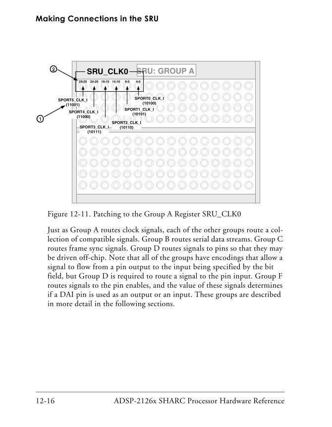
Making Connections in the SRU
12-16 ADSP-2126x SHARC Processor Hardware Reference
Just as Group A routes clock signals, each of the other groups route a col-lection of compatible signals. Group B routes serial data streams. Group C routes frame sync signals. Group D routes signals to pins so that they may be driven off-chip. Note that all of the groups have encodings that allow a signal to flow from a pin output to the input being specified by the bit field, but Group D is required to route a signal to the pin input. Group F routes signals to the pin enables, and the value of these signals determines if a DAI pin is used as an output or an input. These groups are described in more detail in the following sections.
Figure 12-11. Patching to the Group A Register SRU_CLK0
SRU: GROUP ASRU_CLK0
SPORT5_CLK_I(11001)
SPORT4_CLK_I(11000)
SPORT3_CLK_I(10111)
SPORT0_CLK_I(10100)
SPORT1_CLK_I(10101)
SPORT2_CLK_I(10110)
4:09:514:1019:1524:2029:25

ADSP-2126x SHARC Processor Hardware Reference 12-17
Digital Audio Interface
SRU Connection GroupsThe DAI/SRU has the default configuration shown in Table 12-1. .
There are five separate groups of connections that are used in the SRU. The following sections summarize each groups of connections.
Table 12-1. Default DAI/SRU Configuration (Pin Routing)
Pin Number Signal Name Pin Type
DAI_01 SDATA0A Three-State with programmable Pull-up
DAI_02 SDATA0AB Three-State with programmable Pull-up
DAI_03 SCLK0 Three-State with programmable Pull-up
DAI_04 SFS0 Three-State with programmable Pull-up
DAI_05 SDATA1A Three-State with programmable Pull-up
DAI_06 SDATA1B Three-State with programmable Pull-up
DAI_07 SCLK1 Three-State with programmable Pull-up
DAI_08 SFS1 Three-State with programmable Pull-up
DAI_09 SDATA2A Three-State with programmable Pull-up
DAI_10 SDATA2B Three-State with programmable Pull-up
DAI_11 SDATA2C Three-State with programmable Pull-up
DAI_12 SDATA2D Three-State with programmable Pull-up
DAI_13 SCLK2 Three-State with programmable Pull-up
DAI_14 SFS2 Three-State with programmable Pull-up
DAI_15 SDATA3A Three-State with programmable Pull-up
DAI_16 SDATA3B Three-State with programmable Pull-up
DAI_17 SDATA3C Three-State with programmable Pull-up
DAI_18 SDATA3D Three-State with programmable Pull-up
DAI_19 SCLK3 Three-State with programmable Pull-up
DAI_20 SFS3 Three-State with programmable Pull-up

Making Connections in the SRU
12-18 ADSP-2126x SHARC Processor Hardware Reference
Group A Connections – Clock Signals
Group A is used to route signals to clock inputs. The SPORTs clock inputs (when the SPORTs are in clock slave mode), the clock inputs to the eight IDP channels and the two Precision Clock Generators (PCGs) external sources are selected from the list of Group A sources and set in the Group A registers. When channel 0 of the IDP is configured for PDAP input, the clock source set here is used as the parallel word latch instead of the serial bit clock (Table 12-2).
All unused clock inputs should be set to logic LOW. Any IDP channels that receive clock signals set here will send data to the FIFO. When a SPORT is used as a clock master, setting the unused SPORT clock input to logic LOW improves signal integ-rity. The registers, and input and output signals for group A are shown in Table 12-6.
Table 12-2. Group A Sources – Serial Clock
Signal Inputs Signal Sources
Clock Register Bit field
SRU_CLK0 SPORT0_CLK_ISPORT1_CLK_ISPORT2_CLK_ISPORT3_CLK_ISPORT4_CLK_ISPORT5_CLK_I
• 20 External Pins (DAI_PBxx_O)• 6 Serial Port x Clock Outs
(SPORTx_CLK_O)• 2 Precision Clock Generators (A/B)
(PCG_CLKx_O)• 2 Logic Level (HIGH/LOW)
Options SRU_CLK1 IDP0_CLK_I
IDP1_CLK_IIDP2_CLK_I
SRU_CLK2 IDP3_CLK_IIDP4_CLK_IIDP5_CLK_IIDP6_CLK_IIDP7_CLK_I
SRU_CLK3 PCG_EXTA_IPCG_EXTB_I

ADSP-2126x SHARC Processor Hardware Reference 12-19
Digital Audio Interface
Group B Connections – Data Signals
Group B connections, shown in Table 12-3, are used to route signals to serial data inputs. The serial data inputs to both the A and B channels of the SPORTs and to each of the eight IDP channels are selected from the list of Group B sources and set in the Group B registers. When a SPORT is not configured to receive, the data source set here is ignored. Likewise, when channel 0 of the IDP is used for the PDAP, the serial data source set here is ignored.
Table 12-3. Group B Sources – Serial Data
Signal Inputs Signal Sources
Serial Data Register Bit field
SRU_DAT0 SPORT0_DA_ISPORT0_DB_ISPORT1_DA_ISPORT1_DB_ISPORT2_DA_I
• 20 External Pins (DAI_PBxx_O)• 12 Serial Port x Data Outs
(SPORTx_DB_O)• 2 Logic Level (High/Low) Options
SRU_DAT1 SPORT2_DB_ISPORT3_DA_ISPORT3_DB_ISPORT4_DA_ISPORT4_DB_I
SRU_DAT2 SPORT5_DA_ISPORT5_DB_I
SRU_DAT3 IDP0_DAT_IIDP1_DAT_IIDP2_DAT_IIDP3_DAT_I
SRU_DAT4 IDP4_DAT_IIDP5_DAT_IIDP6_DAT_IIDP7_DAT_I

Making Connections in the SRU
12-20 ADSP-2126x SHARC Processor Hardware Reference
Group C Connections – Frame Sync Signals
Group C connections are used to route signals to frame sync inputs. The SPORT frame sync inputs (when the SPORT is in slave mode) and the frame sync inputs to the eight IDP channels are selected from the list of Group C sources and set in the Group C registers.
Each of the frame sync inputs specified is connected to a frame sync source based on the 5-bit values described in the Group C frame sync sources, listed in Table 12-4. Thirty-two possible frame sync sources can be connected using the registers SRU_FS0-2 described in Figure A-43 on page A-121 through Figure A-45 on page A-122.
Table 12-4. Group C Sources – Frame Sync
Signal Inputs Signal Sources
Frame Sync Register Bit field
SRU_FS0 SPORT0_FS_ISPORT1_FS_ISPORT2_FS_ISPORT3_FS_ISPORT4_FS_ISPORT5_FS_I
• 20 External Pins (DAI_PBxx_O)• 6 Serial Port FS Output Options
(SPORTx_FS_O)• 2 Precision Frame Sync (A/B) Outputs
(PCG_FSx_O)• 2 Frame Sync Logic Level (High/Low)
Options SRU_FS1 IDP0_FS_I
IDP1_FS_IIDP2_FS_I
SRU_FS2 IDP3_FS_IIDP4_FS_IIDP5_FS_IIDP6_FS_IIDP7_FS_I
ADSP-2126x SHARC Processor Hardware Reference 12-21
Digital Audio Interface
Group D Connections – Pin Signal Assignments
Group D is used to specify any signals that will be driven off-chip by the pin buffers. A pin buffer input (DAI_PBxx_I) is driven as an output from the processor when the pin buffer enable is set (= 1). Note that DAI pins 19 and 20 may be configured as either active high or active low by setting the corresponding invert bit.
Each physical pin (connected to a bonded pad) may be routed via the SRU to any of the outputs of the DAI audio peripherals, based on the 6-bit val-ues listed in Table 12-5. The SRU also may be used to route signals that control the pins in other ways. These signals may be configured for use as flags, timers, precision clock generators, or miscellaneous control signals.
Group D registers are SRU_PIN0-3, described in Figure A-46 on page A-125 through Figure A-49 on page A-126.

Making Connections in the SRU
12-22 ADSP-2126x SHARC Processor Hardware Reference
Table 12-5. Group D Sources – Pin Signal Assignments
Signal Inputs Signal Sources
DAI Pin Register
Bit field
SRU_PIN0 DAI_PB01_IDAI_PB02_IDAI_PB03_IDAI_PB04_IDAI_PB05_I
• 20 External Pins (DAI_PBxx_O)• 12 Serial Port Data Channel Output Options (two
for each SPORT, and one for each Channel A/B) (SPORTx_DB_O)
• 6 Serial Port Clock Output Options (one for each SPORT) (SPORTx_CLK_O)
• 6 Serial Port FS Output Options (one for each SPORT) (SPORTx_FS_O)
• 3 Timers (TIMERx_O)• 6 Flags (FLGxx_O)• 4 Miscellaneous Control B Options (MISCBx_O)• 2 PCG Clock (A/B) Outputs• 2 PCG Frame Sync (A/B) Outputs• 2 Pin Logic Level (High/Low)
Designations
SRU_PIN1 DAI_PB06_IDAI_PB07_IDAI_PB08_IDAI_PB09_IDAI_PB10_I
SRU_PIN2 DAI_PB11_IDAI_PB12_IDAI_PB13_IDAI_PB14_IDAI_PB15_I
SRU_PIN3 DAI_PB16_IDAI_PB17_IDAI_PB18_IDAI_PB19_IDAI_PB20_IDAI_PB19_INVERTDAI_PB20_INVERT

ADSP-2126x SHARC Processor Hardware Reference 12-23
Digital Audio Interface
Group E Connections – Miscellaneous Signals
Group E connections, shown in Table 12-6, are slightly different from the others in that the inputs and outputs being routed vary considerably in function. This group routes control signals (flags, timers, and so on) and provides a means of connecting signals between groups. Signals with names such as MISCxy appear as inputs in Group E, but do not directly feed any peripheral. Rather, they reappear as outputs in Group D and Group F.
Additional connections among Groups D, E, and F provide a surprising amount of utility. Since Group D routes signals off-chip and Group F dic-tates pin direction, these few signal paths enable an enormous number of possible uses and connections for DAI pins. A few examples include:
• One pin’s input can be patched to another pin’s output, allowing board-level routing under software control.
• A pin input can be patched to another pin’s enable, allowing an off-chip signal to gate an output from the processor.
• Any of the DAI pins can be used as interrupt sources or gen-eral-purpose I/O (GPIO) signals.
• Both input and output signals of the timers can be routed to DAI pins. These peripherals are capable of counting in up, down, or elapsed time modes.
• Many types of bidirectional signaling may be created by routing an output of the PCG to a pin enable.
The SRU enables many possible functional changes, both within the pro-cessor as well as externally. Used creatively, it allows system designers to radically change functionality at run time, and potentially to reuse circuit boards across many products.

Making Connections in the SRU
12-24 ADSP-2126x SHARC Processor Hardware Reference
Table 12-6. Group E Sources – Misc. Assignment
Signal Inputs Signal Sources
DAI Pin Register Bit field
SRU_EXT_MISCA MISCA0_IDAI_INT_28FLG13_IMISCA1_IDAI_INT_29MISCA2_IDAI_INT_30FLG14_IMISCA_3_IDAI_INT_31MISCA_4_IMISCA_5_IINV_MISCA4_IINV_MISCA5_IMISCB_0_IDAI_INT_22TIMER0_IMISCB_1_IDAI_INT_23TIMER1_I
• 20 External Pins (DAI_PBxx_O)• 3 Timers (TIMERx_O)• 1 IDP Parallel Input Strobe Output
(PDAP_STRB_O)• 2 Clock A/B Outputs (PCG_CLKx_O)• 2 PCG Frame Sync A/B Outputs
(PCG_FSx_O)• 2 Logic Level (High/Low) Options
SRU_EXT_MISCB MISCB_2_IDAI_INT_24TIMER2_IMISCB_3_IDAI_INT_25FLG10_IMISCB_4_IDAI_INT26FLG11_IMISCB_5_IDAI_INT_27FLG12_I

ADSP-2126x SHARC Processor Hardware Reference 12-25
Digital Audio Interface
Group F – Pin Enable Signals
Group F signals, shown in Table 12-7, are used to specify whether each DAI pin is used as an output or an input by setting the source for the pin buffer enables. When a pin buffer enable (DAI_PBENxx_I) is set (= 1) the signal present at the corresponding pin buffer input (DAI_PBxx_I) is driven off-chip as an output. When a pin buffer enable is cleared (= 0) the signal present at the corresponding pin buffer input is ignored.
The Pin Enable Control registers activate the drive buffer for each of the 20 DAI pins. When the pins are not enabled (driven), they can be used as inputs.
Table 12-7. Group F Sources – Pin Output Enable
Signal Inputs Signal Sources
DAI Pin Register Bit field
SRU_PBEN0 DAI_PB01_IDAI_PB02_IDAI_PB03_IDAI_PB04_IDAI_PB05_I
• 2 Pin Enable Logic Level (High/Low) Options• 6 Miscellaneous A Control Pins
(MISCAx_O)• 24 Pin Enable Options for 6 Serial Ports (one each for
FS, Data Channel A/B, and Clock) (SPORTx_CLK_PBEN_O), (SPORTx_FS_PBEN_O), (SPORTx_DA_PBEN_O), (SPORTx_DB_PBEN_O)
• 3 Timer Pin Enables (TIMERx_PBEN_O)• 6 Flags Pin Enables (FLGxx_PBEN_O)
SRU_PBEN1 DAI_PB06_IDAI_PB07_IDAI_PB08_IDAI_PB09_IDAI_PB10_I
SRU_PBEN2 DAI_PB11_IDAI_PB12_IDAI_PB13_IDAI_PB14_IDAI_PB15_I
SRU_PBEN3 DAI_PB16_IDAI_PB17_IDAI_PB18_IDAI_PB19_IDAI_PB20_I

General-Purpose I/O (GPIO) and Flags
12-26 ADSP-2126x SHARC Processor Hardware Reference
General-Purpose I/O (GPIO) and Flags Any of the DAI pins may also be considered general-purpose input/output (GPIO) pins. Each of the DAI pins can also be set to drive a high or low logic level signal to assert signals. They can also be connected to miscella-neous signals and used as interrupt sources or as control inputs to other blocks. Other than these, out of the 16 flags available, six (10:15) can use 20 DAI pins.
Miscellaneous SignalsIn a standard SHARC processor, a clock out connects to a clock in. Like-wise, a frame sync out is connected to a frame sync in, and a data out is connected to a data in, and so on. In the ADSP-2126x processor, there are exceptions to these standard connection practices. Signals:
• May also be configured as interrupt sources
• Can be configured as invert signals (forcing a signal to active low)
• Can connect one pin to another
• Can be configured as pin enables
DAI Interrupt ControllerThe DAI contains a dedicated Interrupt Controller that signals the core when DAI-peripheral events have occurred.
Relationship to the CoreGenerally, interrupts are classified as catastrophic or normal. Catastrophic events include any hardware interrupts (for example, resets) and emula-tion interrupts (under the control of the PC), math exceptions, and

ADSP-2126x SHARC Processor Hardware Reference 12-27
Digital Audio Interface
“reads” of memory that do not exist. Catastrophic events are treated as high priority events. In comparison, normal interrupts are “determinis-tic”—specific events emanating from a source (the causes), the result of which is the generation of an interrupt. The expiration of a timer can gen-erate an interrupt, a signal that a serial port has received data that must be processed, a signal that an SPI has either transmitted or received data, and other software interrupts like the insertion of a trap that causes a break-point—all are conditions which identify to the core that an event has occurred.
Since DAI-specific events generally occur infrequently, the DAI IC classi-fies such interrupts as either high or low priority interrupts. Within these broad categories, users can indicate which interrupts are high and which are classified as low.
Any interrupt causes a two-cycle stall, since it forces the core to stop pro-cessing an instruction in process, then vector to the Interrupt Service routine (ISR), (which is basically an Interrupt Vector Table (IVT) lookup), then proceed to implement the instruction referenced in the IVT. For more information, see “Interrupt Vector Addresses” in Appendix B, Interrupt Vector Addresses.
When an interrupt from the DAI must be serviced, one of the two core ISRs must query the DAI’s Interrupt Controller to determine the source(s). Sources can be any one or more of the Interrupt Controller’s 32-configurable channels (DAI_INT[31:0]). For more information, see “DAI Interrupt Controller Registers” on page A-164.
DAI events trigger two interrupts in the primary IVT—one each for low or high priority. When any interrupt from the DAI needs to be serviced, one of the two core ISRs must interrogate the DAI’s Interrupt Controller to determine the source(s).
Reading the DAI’s interrupt latches clears them. Therefore, the ISR must service all the interrupt sources it discovers.

DAI Interrupt Controller
12-28 ADSP-2126x SHARC Processor Hardware Reference
DAI InterruptsThere are several registers in the DAI Interrupt Controller that can be configured to control how the DAI interrupts are reported to and serviced by the core’s Interrupt Controller. Among other options, each DAI inter-rupt can be mapped either as a high or low priority interrupt in the primary interrupt controller, certain DAI interrupts can be triggered on either the rising or falling edge of signals, and each DAI interrupt can also be independently masked.
Just as the core has its own interrupt latch registers (IRPTL and LIRPTL), the DAI has its own latch registers (DAI_IRPTL_L and DAI_IRPTL_H). When a DAI interrupt is configured to be high priority, it is latched in the DAI_IRPTL_H register. When any bit in the DAI_IRPTL_H register is set (= 1), bit 11 in the IRPTL register is also set and the core services that interrupt with high priority. When a DAI interrupt is configured to be low priority, it is latched in the DAI_IRPTL_L register. Similarly, when any bit in the DAI_IRPTL_L register is set (= 1), bit 6 in the LIRPTL register is also set and the core services that interrupt with low priority. Regardless of the priority, when a DAI interrupt is latched and promoted to the core interrupt latch, the ISR must query the DAI’s Interrupt Controller to determine the source(s). Sources can be any one or more of the Interrupt Controller’s 32-configurable channels (DAI_INT[31:0]). For more infor-mation, see “DAI Interrupt Controller Registers” on page A-164.
Reading the DAI’s interrupt latches clears them. Therefore, the ISR must service all the interrupt sources it discovers. That is, if multiple interrupts are latched in one of the DAI_IRPTL_x registers, all of them must be serviced before executing an RTI instruction.
The IDP_FIFO_GTN_INT interrupt is not cleared when the DAI_IRPTL_H/L registers are read. This interrupt is cleared automat-ically when the situation that caused of the interrupt goes away.

ADSP-2126x SHARC Processor Hardware Reference 12-29
Digital Audio Interface
High and Low Priority Latches In the ADSP-2126x, a pair of registers (DAI_IRPTL_H and DAI_IRPTL_L) replace functions normally performed by the IRPTL register. A single regis-ter (DAI_IRPTL_PRI) specifies the latch to which each of these interrupts are mapped.
Two registers (DAI_IRPTL_RE and DAI_IRPTL_FE) replace the DAI periph-eral’s version of the IMASK register. As with the IMASK register, these DAI registers provide a way to specify which interrupts to notice and handle, and which interrupts to ignore. These dual registers function like IMASK does, but with a higher degree of granularity.
Signals from the SRU can be used to generate interrupts. For example, when SRU_EXTMISCA2_INT (bit 30) or DAI_IRPTL_H is set to one, any signal from the external miscellaneous Channel 2 generates an interrupt. If set to one, DAI interrupts trigger an interrupt in the core and the interrupt latch is set. A read of this bit does not reset it to zero. The bit is only set to zero when the cause of the interrupt is cleared. A DAI interrupt indicates the source (in this case, external miscellaneous A, Channel 2), and checks the IVT for an instruction (next operation) to perform.
The 32 interrupt signals within the Interrupt Controller are mapped to two interrupt signals in the primary Interrupt Controller of the SHARC core. The DAI_IRPT_PRI register specifies if the Interrupt Controller inter-rupt is mapped to the high or low core interrupt (1 = high priority and 0 = low priority).
The DAI_IRPTL_H register is a read-only register with bits set for every DAI interrupt latched for the high priority core interrupt. The DAI_IRPTL_L register is a read-only register with bits set for every DAI interrupt latched for the low priority core interrupt. When a DAI interrupt occurs, the low or high priority core ISR should interrogate its corresponding register to determine which of the 32 interrupt sources to service. When the DAI_IRPTL_H register is read, the high priority latched interrupts are all

DAI Interrupt Controller
12-30 ADSP-2126x SHARC Processor Hardware Reference
cleared. When the DAI_IRPTL_L register is read, the low priority latched interrupts are all cleared.
Rising and Falling Edge MasksFor interrupt sources that correspond to waveforms (as opposed to DAI event signals such as DMA complete or buffer full), the edge of a wave-form may be used as an interrupt source as well. Just as interrupts can be generated by a source, interrupts can also be generated latched on the ris-ing (or falling) edges of a signal. This concept does not exist in the main Interrupt Controller, only in the DAI Interrupt Controller.
When a signal comes in, the system needs to determine what kind of sig-nal it is and what kind of protocol, as a result, to service. The preamble indicates the signal type. When the protocol changes, output (signal) type is noted.
For audio applications, the ADSP-2126x needs information about inter-rupt sources that correspond to waveforms (not event signals). As a result, the falling edge of the waveform may be used as an interrupt source as well. Programs may elect to use any of four conditions:
• Latch on the rising edge
• Latch on the falling edge
• Latch on both the rising and falling edge
The DAI Interrupt Controller may be configured using three registers. Each of the 32 interrupt lines can be independently configured to trigger in response to the incoming signal’s rising edge, its falling edge, both the rising edge and the falling edge, or neither the rising edge nor the falling edge. Setting a bit in either the DAI_IRPTL_RE or DAI_IRPTL_FE registers enables the interrupt level on the rising and falling edges, respectively. For more information on these registers, see Figure A-76 on page A-169 and Figure A-76 on page A-169.

ADSP-2126x SHARC Processor Hardware Reference 12-31
Digital Audio Interface
Programs can manage responses to signals by configuring registers. In a sample audio application, for example, upon detection of a change of pro-tocol, the output can be muted. This change of output and the resulting behavior (causing the sound to be muted) results in an alert signal (an interrupt) being introduced in response (if the detection of a protocol change is a high priority interrupt).
The DAI_IRPTL_FE register can only be used for latching interrupts on the falling edge.
Use of the DAI_IRPT_RE or DAI_IRPT_FE registers allows programs to notice and respond to rising edges, falling edges, both rising and falling edges, or neither rising nor falling edges so they can be masked separately.
Enabling responses to changes in condition signals (including changes in DMA state, introduction of error conditions, and so on) can only be enabled using the DAI_IRPT_RE register.
Using the SRU() MacroAs discussed above, the Signal Routing Unit is controlled by writing val-ues that correspond to signal sources into bit fields that further correspond to signal inputs. The SRU is arranged into functional groups such that the registers that are made up of these bit fields accept a common set of source signal values.
In order to ease the coding process, the include file sru2126x.h, is included with the VisualDSP++ tools. This file implements a macro that abstracts away most of the work of signal assignments and functions.
The macro has identical syntax in C/C++ and assembly, and makes a sin-gle connection from an output to an input:
SRU(OutputSignal,InputSignal);

Using the SRU() Macro
12-32 ADSP-2126x SHARC Processor Hardware Reference
The names passed to the macro are the names given in Table 12-2 through Table 12-7 and in the DAI registers section in “Signal Routing Unit Reg-isters” on page A-111. Note that each processor has its own specific version of the macro that implements the bit field encodings appropriate to that part. For example, in code for the ADSP-21262 processor, add the following line in your source code:
#include <sru21262.h>;
The following lines illustrate how the macro is used:/* Route SPORT 1 clock output to pin buffer 5 input */
SRU(SPORT1_CLK_O,DAI_PB05_I);
/* Route pin buffer 14 out to IDP3 frame sync input */
SRU(DAI_PB14_O,IDP3_FS_I);
/* Connect pin buffer enable 19 to logic low */
SRU(LOW,PBEN19_I);
Additional example code is available on the Analog Devices Web site.
There is a macro that has been created to connect peripherals used in a DAI configuration. This code can be used in both Assembly and C code. See the INCLUDE file SRU.H.

ADSP-2126x SHARC Processor Hardware Reference 13-1
13 PRECISION CLOCK GENERATOR
The Precision Clock Generator (PCG) consists of two units, each of which generates a pair of signals derived from a clock input signal. The pair of units, A and B, are identical in functionality and operate indepen-dently of each other. Each unit generates two signals that are normally used as a clock frame sync pair. The unit that generates the clock is rela-tively simple, since digital clock signals are usually regular and symmetrical. The unit that generates the frame sync output, however, is designed to be extremely flexible and capable of generating the wide vari-ety of framing signals needed by the many types of peripherals that can be connected to the signal routing unit (SRU). For more information, see “Signal Routing Unit” on page 12-3.
The core phase locked loop (PLL) has been designed to provide clocking for the processor core. Although the performance specifications of this PLL are appropriate for the core, they have not been optimized or speci-fied for precision data converters where jitter directly translates into time quantization errors and distortion.
The PCG can accept its clock input either directly from the external oscil-lator (or discrete crystal) connected to the CLKIN/XTAL pins or from any of the 20 DAI pins. This allows a design to contain an external clock with performance specifications appropriate for the application target.

13-2 ADSP-2126x SHARC Processor Hardware Reference
Note that any clock and frame sync signals generated by the serial ports are also subject to these jitter problems because the SPORT clock is gener-ated from the core clock. However, a SPORT can produce data output while being a clock and frame sync slave. The clock generated by the SPORT is sufficient for most serial communications, but it is suboptimal for analog conversion. Therefore, all precision data converters should be synchronized to a clock generated by the PCG or to a clean (low jitter) clock that is fed into the SRU off-chip via a pin.
Any clock or frame sync unit should be disabled (have its enable bit cleared) before changing any of the associated parameters. After disabling PCG, delay of N core clock cycles (N = PCG source clock period/CLKIN period) should be provided before programming PCG with new parameters.
Figure 13-1. Clock Inputs
COREPLL
SHARC ADSP-2126x
PRECISIONCLOCK
GENERATOR
M/NCORE CLOCKGENERATOR
SPORTSRU
CORECORE CLOCKBUFFER
AMP
EXTERNALOSCILLATOR
EXTERNALOSCILLATOR
OR XTAL
CLKIN

ADSP-2126x SHARC Processor Hardware Reference 13-3
Precision Clock Generator
Clock OutputsAs stated in the overview, each of the two units (A and B) produces a clock output and a frame sync output. The clock output is derived from the input to the PCG with a 20-bit divisor.
If the divisor is either zero or one, the PCG’s clock generation unit is bypassed, and the clock input is connected directly to the clock output. Otherwise, the PCG unit clock output frequency is equal to the input clock frequency, divided by a 20-bit integer. The integer is specified in the CLKADIV bit field (bits 19–0 of the PCG_CTLA_1 register) for unit A and a corresponding bit field in the PCG_CTLB_1 register for unit B. See also Figure A-57 on page A-141 and Figure A-59 on page A-143.
The clock outputs have two other control bits that enable the A and B units, ENCLKA and ENCLKB, respectively (bits 31 of the PCG_CTLA_0 and PCG_CTLB_0 registers). These bits enable (= 1) and disable (= 0) the clock output signal for units A and B, respectively. When disabled, clock output is held at logic low.
The CLKASOURCE bit (bit 31 in the PCG_CTLA_1 register) specifies the input source for the clock of unit A. When this bit is cleared (= 0), the input is sourced from the external oscillator, as shown in Figure 13-1. When set (= 1), the input is sourced from the SRU, as specified in the SRU_CLK3 register in PCG_EXTA_I (bits 4–0). See Table A-41 on page A-141.
The PCG unit B functions identically, except that the PCG_CTLB_1 bit (bit 31) indicates that the external source for unit B is specified in PCG_EXTB_I (bits 9–5 of the SRU_CLK3 register). See Table A-44 on page A-144.
Note that the clock output is always set (as closely as possible) to a 50% duty cycle. If the clock divisor is even, the duty cycle of the clock output is exactly 50%. If the clock divisor is odd, then the duty cycle is slightly less
Frequency of Clock Output = Frequency of Clock Input
Clock Divisor
Frame Sync Outputs
13-4 ADSP-2126x SHARC Processor Hardware Reference
than 50%. The low period of the output clock is one input clock period more than the high period of the output clock.
A PCG clock output cannot be fed to its own input. Setting SRU_CLK3[4:0] = 28 connects PCG_EXTA_I to logic low, not to PCG_CLKA_O. Setting SRU_CLK3[9:5] = 29 connects PCG_EXTB_I to logic low, not to PCG_CLKB_0.
Frame Sync OutputsEach of the two units (A and B) also produces a synchronization signal for framing serial data. The frame sync outputs are much more flexible since they need to accommodate the wide variety of serial protocols used by peripherals.
There are two modes of operation for the PCG frame sync. The divisor field determines if the frame sync will operate in Normal mode (divisor > 1) or Bypass mode (divisor = 0 or 1).
Frame SyncFor a given frame sync, the output is determined by the following:
• Divisor. A 20-bit divisor of the input clock that determines the period of the frame sync. When set to zero or one, the frame sync operates in Bypass mode, otherwise it operates in Normal mode.
• Phase. A 20-bit value that determines the phase relationship between the clock output and the frame sync output. Settings for phase can be anywhere between zero to DIV - 1.

ADSP-2126x SHARC Processor Hardware Reference 13-5
Precision Clock Generator
• Pulse width. A 16-bit value that determines the width of the fram-ing pulse. Settings for pulse width can be zero to DIV-1. If the pulse width is equal to zero, then the actual pulse width of the output frame sync is:
The frequency of the frame sync output is determined by:
When the divisor is set to any value other than zero or one, the ADSP-2126x operates in Normal mode.
The frame sync A divisor is specified in bits 19–0 of the PCG_CTLA_0 register and the frame sync B divisor is specified in bits 19–0 of the PCG_CTLB_0 register. The pulse width of frame sync output is equal to the number of input clock periods specified in the 16-bit field of the PCG_PW register. Bits 15–0 specify the pulse width of frame sync A, and bits 31–16 specify the pulse width of frame sync B.
Frame Sync Output Synchronization with External Clock
The frame sync output may be synchronized with an external clock by programming the SRU_EXT_MISCA, SRU_CLK2 and SRU_CLK3 registers appro-priately. In this mode, the PCG frame sync output is synchronized with the rising edge of the external clock (shown in Figure 13-2). The external clock is routed to the PCG block from any of the SRU group E sources
Frame Sync Divisor
2For even divisors:
Frame Sync Divisor – 1
2For odd divisors:
Frequency of Frame Sync Output =Frequency of Clock Input
Frame Sync Divisor

Frame Sync Outputs
13-6 ADSP-2126x SHARC Processor Hardware Reference
through the MISCA4_I (for PCGA) and MISCA5_I (for PCGB) signals of the SRU_EXT_MISCA register. For more information, see “Miscellaneous SRU Registers (SRU_EXT_MISCx, Group E)” on page A-130.
Synchronization with the external clock is enabled by setting bit 25 of the SRU_CLK2 register for PCGA frame sync output and bit 10 of the SRU_CLK3 register for PCGB frame sync output. For more information, see “Clock Routing Control Registers (SRU_CLKx, Group A)” on page A-112. The phase must be programmed to three, so that the rising edge of the external clock is in sync with the frame sync. Programming should occur in the fol-lowing order:
1. Program PCG control registers SRU_EXT_MISCA, SRU_CLK2 and SRU_CLK3 as mentioned above.
2. Enable the clock, frame sync, or both. In other words, program all the values before enabling the PCG (clock and frame sync).
Since the rising edge of the external clock is used to synchronize with the frame sync, the frame sync output is not generated until a rising edge of the external clock is sensed.
The clock output cannot be aligned with the rising edge of the external clock as there is no phase programmability. Once CLKA and CLKB have been enabled, by programming bit 31 of PCG_CTLA_0 and PCG_CTLB_0 registers
Figure 13-2. Clock Output Synchronization with External Clock
FSA(OUTPUT)
PCGx_CLKIN
EXT CLK(INPUT)

ADSP-2126x SHARC Processor Hardware Reference 13-7
Precision Clock Generator
respectively, these outputs are activated when a low to high transition is sensed in the external clock (MISCA4_I, MISCA5_I).
Phase ShiftAnother PCG frame sync parameter provides for phase shifting with respect to the clock of the same unit. This feature allows shifting in time relative to clock signals. Frame sync phase shifting is often required by
peripherals that need to lead or lag a clock signal. For example, the I2S protocol specifies that the frame sync should transition from high to low
one clock cycle before the beginning of a frame. Since an I2S frame is 64 clock cycles long, delaying the frame sync by 63 cycles produces the required framing.
The amount of phase shifting is specified as a 20-bit value in the FSAPHASE_HI bit field (bits 29–20) of the PCG_CTLA_O register and in the FSAPHASE_LO bit field (bits 29–20) of the PCG_CTLA_1 register for unit A. A single 20-bit value spans these two bit fields. The upper half of the word [19:10] is in the PCG_CTLA_O register, and the lower half [9:0] is in the PCG_CTLA_1 register.
Similarly, the phase shift for frame sync B is specified in the PCG_CTLB_O and PCG_CTLB_1 registers.
When using a clock and frame sync as a synchronous pair, the units must be enabled in a single atomic instruction before their parame-ters are modified. Both units must also be disabled in a single atomic instruction.

13-8 ADSP-2126x SHARC Processor Hardware Reference
Phase Shift SettingsThe phase shift between clock and frame sync outputs may be pro-grammed under these conditions:
• The input clock source for the clock generator output and the frame sync generator output is the same.
• Clock and frame sync are enabled at the same time using a single atomic instruction.
• Frame sync divisor is an integral multiple of the clock divisor.
If the phase shift is zero, the clock and frame sync outputs rise at the same time. If the phase shift is one, the frame sync output transitions one input clock period ahead of the clock transition. If the phase shift is DIVISOR – 1, the frame sync transitions DIVISOR – 1 input clock periods ahead of the clock transitions. This translates to the input clock period after the clock transition, which further translates to one input clock period after the clock transition.
Phase shifting is represented as a full 20-bit value so that even when frame sync is divided by the maximum amount, the phase can be shifted to the full range, from zero to one input clock short of the period.

ADSP-2126x SHARC Processor Hardware Reference 13-9
Precision Clock Generator
Pulse WidthPulse width is the number of input clock periods for which the frame sync output is HIGH. Pulse width should be less than the divisor of the frame sync. The pulse width of frame sync A is specified in bits 15–0 of the PCG_PW register and the pulse width of frame sync B is specified in bits 31–16 of the PCG_PW register.
Figure 13-3. Adjusting Frame Sync Phase Shift
FRAME SYNC OUTPUT(PHASE SHIFT = DIVISOR -1)
CLOCK INPUT(FOR BOTH CLOCKAND FRAME SYNC)
ENABLE
FRAME SYNC OUTPUT(PHASE SHIFT = 0)
FRAME SYNC OUTPUT(PHASE SHIFT = 1)
CLOCK OUTPUT
FRAME SYNC OUTPUT(PHASE SHIFT = 2)
OTHER VALUES:
CLOCK DIVISOR = 2FRAME SYNC DIVISOR = 8PULSE WIDTH = 4

13-10 ADSP-2126x SHARC Processor Hardware Reference
If the pulse width is equal to zero, then the actual pulse width of the frame sync output is equal to:
if the divisor is even, or
if the divisor is odd.
Bypass ModeWhen the divisor for the frame sync has a value of zero or one, the frame sync is in Bypass mode, and the PCG_PW register has different functionality than in Normal mode. Two bit fields determine the operation in this mode. The One Shot Frame Sync A or B (STROBEx) bit (bits 0 and 16, respectively) determines if the frame sync has the same width as the input, or of a single strobe. These bits also determine whether the Active Low Frame Sync Select for the Frame Sync A or B (INVFSx) bit (bits 1 and 17, respectively) inverts the input. For additional information about the PCG_PW register, see Figure A-60 on page A-144.
In Bypass mode, bits 15–2 and bits 31–18 of the PCG_PW register are ignored.
Bypass as a Pass Through
When the STROBEA bit in the PCG_PW register for unit A or the STROBEB bit in the PCG_PW register for unit B equals zero, the unit is bypassed and the output equals the input. If INVFSA (bit 1) for unit A or INVFSB (bit 17) for unit B is set, then the signal is inverted.
Bypass mode also enables the generation of a strobe pulse (“one shot”). Strobe usage ignores the counter and looks to the SRU to provide the input signal.
DIVISOR2
DIVISOR – 12

ADSP-2126x SHARC Processor Hardware Reference 13-11
Precision Clock Generator
Bypass as a One Shot
When the STROBEA bit (bit 0 of the PCG_PW register) or STROBEB bit (bit 16 of the PCG_PW register) is set (= 1), the One Shot option is used. When the STROBEx bit is set (= 1), the frame sync is a pulse with a duration equal to one period, or one full cycle, of MISCA2_I for unit A and MISCA3_I for unit B that repeats at the beginning of every clock input period. This pulse is generated during the high period when the INVFSA/B bits (bits 1 or 17, respectively = 0), are cleared or low period when invert bit (INVFSA/B = 1) of the input clock.
A strobe period is equal to the period of the normal clock input signal spec-ified by FSASOURCE (bit 30 in the PCG_CTLA_1 register for unit A) and FSBSOURCE (bit 30 in the PCG_CTLB_1 register for unit B).
The output pulse width is equal to the period of the SRU source signal (MISCA2_I for frame sync A and MISCB3_I for frame sync B). The pulse begins at the second rising edge of MISCxx_I following a rising edge of the clock input. When the INVFSA/B bit is set, the pulse begins at the second rising edge of MISCxx_I coincident or following a falling edge of the clock input.
For more information, see “Group E Connections – Miscellaneous Sig-nals” on page 12-23.
Figure 13-4. Frame Sync Bypass
CLOCK INPUTFOR FRAME SYNC
FRAME SYNC OUTPUT(INVFSA = 0, STROBEA = 0)
FRAME SYNC OUTPUT(INVFSA = 1, STROBEA = 0)

PCG Programming Examples
13-12 ADSP-2126x SHARC Processor Hardware Reference
The second INVFSA bit (bit 1) of the Pulse Width Control (PCG_PW) regis-ter determines whether the falling or rising edge is used. When set (= 1), this bit selects an active low frame sync, and the pulse comes during the low period of clock input. When cleared (= 0) this bit is set to active high frame sync and the pulse comes during the high period of clock input. For more information on the PCG_PW register, refer to Table A-44 on page A-144.
PCG Programming ExamplesThis section provides two programming examples written for the ADSP-21262 processor. The first listing, Listing 13-1, uses PCG channel B to output a clock on DAI pin 1 and frame sync on DAI pin 2. The input used to generate the clock and frame sync is CLKIN. This example demon-strates the clock and frame sync divisors, as well as the pulse width and phase shift capabilities of the PCG.
The second listing, Listing 13-2, uses both PCG channels. Channel A is set up to only generate a clock signal. This clock signal is used as the input to channel B via the SRU. The clock and frame sync are routed to DAI pins 1 and 2, respectively, in the same manner as the first example. This
Figure 13-5. One Shot (Synchronous Clock Input and MISCA2_I)
CLOCK INPUTFOR FRAME SYNC
MISCA2_I
FRAME SYNC OUTPUT(INVFSA = 0, STROBEA = 1)
FRAME SYNC OUTPUT(INVFSA = 1, STROBEA = 1)

ADSP-2126x SHARC Processor Hardware Reference 13-13
Precision Clock Generator
frame sync generated in this example is set for a 50% duty cycle, with no phase shift.
Listing 13-1. PCG Channel B Output Example
/* Register definitions */
#define SRU_CLK3 0x2434
#define SRU_PIN0 0x2460
#define SRU_PBEN0 0x2478
#define PCG_CTLB1 0x24C3
#define PCG_CTLB0 0x24C2
#define PCG_PW 0x24C4
/* SRU definitions */
#define PCG_CLKB_P 0x39
#define PCG_FSB_P 0x3B
#define PBEN_HIGH_Of 0x01
//Bit Positions
#define DAI_PB02 6
#define PCG_PWB 16
/* Bit definitions */
#define ENFSB 0x40000000
#define ENCLKB 0x80000000
/* Main code section */
.global _main;
.section/pm seg_pmco;
_main:
/* Route PCG Channel B clock to DAI Pin 1 via SRU */
/* Route PCG Channel B frame sync to DAI Pin 2 via SRU */
r0 = PCG_CLKB_P|(PCG_FSB_P<<DAI_PB02);
dm(SRU_PIN0) = r0;

PCG Programming Examples
13-14 ADSP-2126x SHARC Processor Hardware Reference
/* Enable DAI Pins 1 & 2 as outputs */
r0 = PBEN_HIGH_Of|(PBEN_HIGH_Of<<DAI_PB02);
dm(SRU_PBEN0) = r0;
r0 = (100<<PCG_PWB); /* PCG Channel B FS Pulse width = 100 */
dm(PCG_PW) = r0;
r2 = 1000; /* Define 20-bit Phase Shift */
r0 = (ENFSB|ENCLKB| /*Enable PCG Channel B Clock and FS*/
1000000); /* FS Divisor = 1000000 */
r1 = lshift r2 by -10;
/* Deposit the upper 10-bits of the Phase Shift in the */
/* correct position in PCG_CTLB0 (Bits 20-29) */
r1 = fdep r1 by 20:10;
r0 = r0 or r1; /* Phase Shift 10-19 = 0 */
dm(PCG_CTLB1) = r0;
dm(PCG_CTLB0) = r0;
r0 = (100000); /* Clk Divisor = 100000 */
/* Use CLKIN as clock source */
/* Deposit the lower 10-bits of the Phase Shift in the */
/* correct position in PCG_CTLB1 (Bits 20-29) */
r1 = fdep r2 by 20:10;
r0 = r0 or r1; /* Phase Shift 10-19 = 0x3E8 */
dm(PCG_CTLB1) = r0;
//----------------------------------------
_main.end: jump(pc,0);
Listing 13-2. PCG Channel A and B Output Example
/* Register Definitions */
#define SRU_CLK3 0x2434

ADSP-2126x SHARC Processor Hardware Reference 13-15
Precision Clock Generator
#define SRU_PIN0 0x2460
#define SRU_PBEN0 0x2478
#define PCG_CTLA1 0x24C1
#define PCG_CTLA0 0x24C0
#define PCG_CTLB1 0x24C3
#define PCG_CTLB0 0x24C2
#define PCG_PW 0x24C4
/* SRU Definitions */
#define PCG_CLKA_O 0x1c
#define PCG_CLKB_P 0x39
#define PCG_FSB_P 0x3B
#define PBEN_HIGH_Of 0x01
//Bit Positions
#define PCG_EXTB_I 5
#define DAI_PB02 6
#define PCG_PWB 16
/* Bit Definitions */
#define ENCLKA 0x80000000
#define ENFSB 0x40000000
#define ENCLKB 0x80000000
#define CLKBSOURCE 0x80000000
#define FSBSOURCE 0x40000000
/* Main code section */
.global _main; /* Make main global to be accessed by ISR */
.section/pm seg_pmco;
_main:
/*Route PCG Channel A clock to PCG Channel B Input via SRU*/
r0 = (PCG_CLKA_O<<PCG_EXTB_I);
dm(SRU_CLK3) = r0;

PCG Programming Examples
13-16 ADSP-2126x SHARC Processor Hardware Reference
/* Route PCG Channel B clock to DAI Pin 1 via SRU */
/* Route PCG Channel B frame sync to DAI Pin 2 via SRU */
r0 = (PCG_CLKB_P|(PCG_FSB_P<<DAI_PB02));
dm(SRU_PIN0) = r0;
/* Enable DAI Pins 1 & 2 as outputs */
r0 = (PBEN_HIGH_Of|(PBEN_HIGH_Of<<DAI_PB02));
dm(SRU_PBEN0) = r0;
r0 = ENCLKA; /* Enable PCG Channel A Clock, No Channel A FS */
/* FS Divisor = 0, FS Phase 10-19 = 0 */
dm(PCG_CTLA0) = r0;
r1 = 0xfffff; /* Clk Divisor = 0xfffff, FS Phase 0-9 = 0 */
/* Use CLKIN as clock source */
dm(PCG_CTLA1) = r1;
r0 = (5<<PCG_PWB); /* PCG Channel B FS Pulse width = 1 */
dm(PCG_PW) = r0;
r0 = (ENFSB|ENCLKB|10); /*Enable PCG Channel B Clock and FS*/
/* FS Divisor = 10, FS Phase 10-19 = 0 */
dm(PCG_CTLB0) = r0;
r0 = (CLKBSOURCE|FSBSOURCE|10); /* Clk Divisor = 10 */
/* FS Phase 0-9 = 0, Use SRU_MISC4 as clock source */
dm(PCG_CTLB1) = r0;
_main.end: jump(pc,0);

ADSP-2126x SHARC Processor Hardware Reference 14-1
14 PERIPHERAL TIMER
In addition to the internal core timer, the ADSP-2126x contains three identical 32-bit timers that can be used to interface with external devices. Each timer can be individually configured in any of three modes:
• “Pulse Width Modulation Mode (PWM_OUT)” on page 14-7
• “Pulse Width Count and Capture Mode (WDTH_CAP)” on page 14-10
• “Pulse Width Count and Capture Mode (WDTH_CAP)” on page 14-10
Timer ArchitectureEach timer has one dedicated bidirectional chip signal, TIMERx. The three timer signals are connected to the 20 Digital Audio Interface (DAI) pins through the Signal Routing Unit (SRU). The timer signal functions as an output signal in PWM_OUT mode and as an input signal in WDTH_CAP and EXT_CLK modes. To provide these functions, each timer has four, 32-bit registers. The registers for each timer are:
• Timer x Configuration (TMxCTL) register
• Timer x Word Count (TMxCNT) register
• Timer x Word Period (TMxPRD) register
• Timer x Word Pulse Width (TMxW) register

Timer Architecture
14-2 ADSP-2126x SHARC Processor Hardware Reference
The timers also share one common status and control register, the Timer Global Status and Control (TMSTAT) register.
For information on the Timer registers, see “Peripheral Timer Registers” on page A-155.
When clocked internally, the clock source is the ADSP-2126x’s core clock (CCLK). The timer produces a waveform with a period equal to 2 x TMxPRD and a width equal to 2 x TMxW. The period and width are set
Figure 14-1. Timer Block Diagram
U
SUB
PERIOD
COUNT
PULSE WIDTH
PERIOD BUFFER PULSE WIDTH BUFFER
32 (READ-ONLY)
3232
–
EXPIRE
I/O MEMORY DATA BUS
+

ADSP-2126x SHARC Processor Hardware Reference 14-3
Peripheral Timer
through the TMxPRD[30:0] and the TMxW[30:0] bits. Bit 31 is ignored for both. Assuming CCLK = 200 MHz:
maximum period = 2 x (231 – 1) x 5 ns = 20 seconds.
Timer Status and ControlThe Timer Global Status and Control (TMSTAT) register indicates the sta-tus of all three timers using a single read. The TMSTAT register also contains timer enable bits. Within TMSTAT, each timer has a pair of sticky Status bits, that require a write one-to-set (TIMxEN) or write one-to-clear (TIMxDIS) to enable and disable the timer respectively.
Writing a one to both bits of a pair disables that timer.
Each timer also has an Overflow Error Detection bit, TIMxOVF. When an overflow error occurs, this bit is set in the TMSTAT register. A program must write one-to-clear this bit.
See Table 14-1 for more information about bits in the TMSTAT register.

Timer Status and Control
14-4 ADSP-2126x SHARC Processor Hardware Reference
After the timer has been enabled, its TIMxEN bit is set (= 1). The timer then starts counting three core clock cycles after the TIMxEN bit is set. Setting (writing one to) the timer’s TIMxDIS bit stops the timer without waiting for another event.
Timer InterruptsEach timer generates a unique interrupt request signal. A common register latches these interrupts so that a program can determine the interrupt
Table 14-1. Timer Global Status and Control (TMSTAT) Register Bits
Bit(s) Name Definition
0 TIM0IRQ Timer 0 Interrupt Latch Write one-to-clear (also an output)1
1 TIM1IRQ Timer 1 Interrupt Latch Write one-to-clear (also an output)1
2 TIM2IRQ Timer 2 Interrupt Latch Write one-to-clear (also an output)1
3 Reserved
4 TIM0OVF Timer 0 Overflow/Error Write one-to-clear (also an output)
5 TIM1OVF Timer 1 Overflow/Error Write one-to-clear (also an output)
6 TIM2OVF Timer 2 Overflow/Error Write one-to-clear (also an output)
7 Reserved
8 TIM0EN Timer 0 Enable Write one-to-enable Timer 0
9 TIM0DIS Timer 0 Disable Write one-to-disable Timer 0
10 TIM1EN Timer 1 Enable Write one-to-enable Timer 1
11 TIM1DIS Timer 1 Disable Write one-to-disable Timer 1
12 TIM2EN Timer 2 Enable Write one-to-enable Timer 2
13 TIM2DIS Timer 2 Disable Write one-to-disable Timer 2
31–14 Reserved
1 This bit is set to one when an interrupt generating event occurs. When the program writes a one to this bit position, it clears the source event which causes this bit to clear. A subsequent read of this bit will return a zero.

ADSP-2126x SHARC Processor Hardware Reference 14-5
Peripheral Timer
source without reference to the timer’s interrupt signal. The TMSTAT regis-ter contains an Interrupt Latch bit (TIMxIRQ) and an Overflow/Error Indicator bit (TIMxOVF) for each timer.
The three timer interrupts are connected as follows:
• TIM0IRQ to GPTMR0I, bit 13 in the IRPTL register
• TIM1IRQ to GPTMR1I, bit 4 in the LIRPTL register
• TIM2IRQ to GPTMR2I, bit 8 in the LIRPTL register
These sticky bits are set by the timer hardware and may be watched by software. They need to be cleared in the TMSTAT register by software explic-itly. To clear, write a one to the corresponding bit in the TMSTAT register.
Interrupt and overflow bits may be cleared simultaneously with timer enable or disable.
To enable a timer’s interrupt, set the IRQEN bit in the timer’s Configura-tion (TMxCTL) register and unmask the timer’s interrupt by setting the corresponding bit of the IMASK register. With the IRQEN bit cleared, the timer does not set its Interrupt Latch (TIMxIRQ) bits. To poll the TIMxIRQ bits without generating a timer interrupt, programs can set the IRQEN bit while leaving the timer’s interrupt masked.
With interrupts enabled, ensure that the interrupt service routine (ISR) clears the TIMxIRQ latch before the RTI instruction to assure that the inter-rupt is not serviced erroneously. In External Clock (EXT_CLK) mode, the latch should be reset at the very beginning of the interrupt routine so as not to miss any timer event.
Enabling a TimerTo enable an individual timer, set the timer’s TIMxEN bit in the TMSTAT reg-ister. To disable an individual timer, set the timer’s TIMxDIS bit in the

Enabling a Timer
14-6 ADSP-2126x SHARC Processor Hardware Reference
TMSTAT register. To enable all three timers in parallel, set all the TIMxEN bits in the TMSTAT register.
Before enabling a timer, always program the corresponding timer’s Con-figuration (TMxCTL) register. This register defines the timer’s operating mode, the polarity of the TIMERx signal, and the timer’s interrupt behav-ior. Do not alter the operating mode while the timer is running. For more information on the TMxCTL register, see “Timer Configuration Registers (TMxCTL)” on page A-156.
The timer enable and disable timing appears in Figure 14-2.
When the timer is enabled, the Count register is loaded according to the operation mode specified in the TMxCTL register. When the timer is dis-abled, the Counter registers retain their state; when the timer is re-enabled, the counter is reinitialized based on the operating mode. The software should never write the counter value directly.
Figure 14-2. Timer PWM Enable and Disable Timing
CCLK
PWMOUT
CCLKTCOUNT
= MTC OUNT= M + 1
TCOUNT= M + 1
TCOUNT= M + 1
TIMER ENABLESET
TIMENTIMER
ENABLED
T MxPRD = 0x2T MxW = 0x1
TCOUNT= XX
TCOUNT= XX
TCOUNT= 1
TCOUNT= 2
TCOUNT= 4
TCOUNT= 3
TIMERDISABLED
TIMER DISABLESET
TIMDIS

ADSP-2126x SHARC Processor Hardware Reference 14-7
Peripheral Timer
Any of the timers can be used to implement a watchdog functionality that can be controlled by either an internal or an external clock source.
For software to service the watchdog, the program must reset the timer value by disabling and then re-enabling the timer. Servicing the watchdog periodically prevents the Count register from reaching the period value and prevents the timer interrupt from being generated. When the timer reaches the period value and generates the interrupt, reset the DSP within the corresponding watchdog’s ISR.
Pulse Width Modulation Mode (PWM_OUT)In PWM_OUT mode, the timer supports on-the-fly updates of period and width values of the PWM waveform. The period and width values can be updated once every PWM waveform cycle, either within or across PWM cycle boundaries.
To enable PWM_OUT mode, set the TIMODE1–0 bits to 01 in the timer’s Con-figuration (TMxCTL) register. This configures the timer’s TIMERx signal as an output with its polarity determined by PULSE as follows:
• If PULSE is set (= 1), an active high width pulse waveform is gener-ated at the TIMERx signal.
• If PULSE is cleared (= 0), an active low width pulse waveform is gen-erated at the TIMERx signal.
The timer is actively driven as long as the TIMODE field remains 01.
Figure 14-3 shows a flow diagram for PWM_OUT mode. When the timer becomes enabled, the timer checks the period and width values for plausi-bility (independent of the value set with the PRDCNT bit) and does not start to count when any of the following conditions are true:
• Width is equal to zero

Enabling a Timer
14-8 ADSP-2126x SHARC Processor Hardware Reference
• Period value is lower than width value
• Width is equal to period
On invalid conditions, the timer sets both the TMxOVF and the TIMIRQx bits and the Count register is not altered. Note that after reset, the timer regis-ters are all zero.
As mentioned earlier, 2 x TMxPRD is the period of the PWM waveform and 2 x TMxW is the width. If the period and width values are valid after the timer is enabled, the Count register is loaded with the value resulting from 0xFFFF FFFF – width. The timer counts upward to 0xFFFF FFF. Instead
Figure 14-3. Timer Flow Diagram - PWM_OUT Mode
DATA BUS
RESET
TIMER_ENABLE
TMxPRD TMxW
CLOCK
YES
INTERRUPT
HIGH
LOW
TMRX
EQUAL?
TMxCNT
YES
PWMOUTLOGIC
EQUAL?
SET PWMOUT

ADSP-2126x SHARC Processor Hardware Reference 14-9
Peripheral Timer
of incrementing to 0xFFFF FFFF, the timer then reloads the counter with the value derived from 0xFFFF FFFF – (period – width) and repeats.
PWM Waveform Generation
If the PRDCNT bit is set, the internally-clocked timer generates rectangular signals with well-defined period and duty cycles. This mode also generates periodic interrupts for real-time DSP processing.
The 32-bit Period (TMxPRD) and Width (TMxW) registers are programmed with the values of the timer count period and pulse width modulated out-put pulse width.
When the timer is enabled in this mode, the TIMERx signal is pulled to a deasserted state each time the pulse width expires, and the signal is asserted again when the period expires (or when the timer is started).
To control the assertion sense of the TIMERx signal, the PULSE bit in the corresponding TMxCTL register is either cleared (causes a low assertion level) or set (causes a high assertion level).
When enabled, a timer interrupt is generated at the end of each period. An ISR must clear the Interrupt Latch bit TIMxIRQ and might alter period and/or width values. In pulse width modulation applications, the software needs to update the period and pulse width values while the timer is running.
When a program updates the timer configuration, the TMxW register must always be written to last, even if it is necessary to update only one of the registers. When the TMxW value is not subject to change, the ISR reads the current value of the TMxW register and rewrite it again. On the next counter reload, all of the timer Control registers are read by the timer.
To generate the maximum frequency on the TIMERx output signal, set the period value to two and the pulse width to one. This makes the TIMERx signal toggle every two CCLK clock cycles.

Enabling a Timer
14-10 ADSP-2126x SHARC Processor Hardware Reference
Single-Pulse Generation
If the PRDCNT bit is cleared, the PWM_OUT mode generates a single pulse on the TIMERx signal. This mode can also be used to implement a well defined software delay that is often required by state machines. The pulse width (= 2 x TMxW) is defined by the width register and the period register is not used.
At the end of the pulse, the Interrupt Latch bit (TIMxIRQ) is set and the timer is stopped automatically. If the PULSE bit is set, an active high pulse is generated on the TIMERx signal. If the PULSE bit is not set, the pulse is active low.
Using a General-Purpose Timer as a Core Timer
Programs can use a general-purpose timer as a core timer. When in this mode, the timer can also generate a periodic interrupt in a fashion similar to the core timer. In this case there is no need to route the timer signal to an external pin.
To implement this behavior, it is necessary to set the TIMODEPWM bits, the PRDCNT bit, and the IRQEN bit in the applicable TMxCTL register. The period at which the interrupt is latched is the pulse period (2 x value in TMxPRD register) in core cycles. Even though the TMxW register is not used in this case, it is necessary to initialize it to a nonzero value less than the value in the TMxPRD register for correct operation.
Unlike the core timer, programs must manually clear the interrupt in the TMSTAT register for each interrupt that is serviced.
Pulse Width Count and Capture Mode (WDTH_CAP)To enable WDTH_CAP mode, set the TIMODE1–0 bits in the TMxCTL register to 10. This configures the TIMERx signal as an input signal with its polarity determined by PULSE. If PULSE is set (= 1), an active high width pulse waveform is measured at the TIMERx signal. If PULSE is cleared (= 0), an

ADSP-2126x SHARC Processor Hardware Reference 14-11
Peripheral Timer
active low width pulse waveform is measured at the TIMERx signal. The internally-clocked timer is used to determine the period and pulse width of externally-applied rectangular waveforms. The Period and Width regis-ters are read-only in WDTH_CAP mode. The period and pulse width measurements are with respect to a clock frequency of CCLK/2.
Figure 14-4 shows a flow diagram for WDTH_CAP mode. In this mode, the timer resets words of the count in the TMxCNT register value to 0x0000 0001 and does not start counting until it detects the leading edge on the TIMERx signal.
Figure 14-4. Timer Flow Diagram – WDTH_CAP Mode
DATA BUS
RESET
SETTMxOVF
BIT
TMxPRD TMxW
CLOCK
INTERRUPT
PRDCNT
TMRx
TMxCNT
1
LEADINGEDGE
DETECT
TMxOVF
TMRxTRAILING
EDGEDETECT
INTERRUPTLOGIC
1
2
2

Enabling a Timer
14-12 ADSP-2126x SHARC Processor Hardware Reference
When the timer detects a first leading edge, it starts incrementing. When it detects the trailing edge of a waveform, the timer captures the current value of the Count register (= TMxCNT/2) and transfers it into the TMxW width registers. At the next leading edge, the timer transfers the current value of the Count register (= TMxCNT/2) into the TMxPRD period register. The Count registers are reset to 0x0000 0001 again, and the timer contin-ues counting until it is either disabled or the count value reaches 0xFFFF FFFF.
In this mode, software can measure both the pulse width and the pulse period of a waveform. To control the definition of the leading edge and trailing edge of the TIMERx signal, the PULSE bit in the TMxCTL register is set or cleared. If the PULSE bit is cleared, the measurement is initiated by a falling edge, the Count register is captured to the Width register on the rising edge, and the Period register is captured on the next falling edge.
The PRDCNT bit in the TMxCTL register controls whether an enabled inter-rupt is generated when the pulse width or pulse period is captured. If the PRDCNT bit is set, the Interrupt Latch bit (TIMxIRQ) gets set when the pulse period value is captured. If the PRDCNT bit is cleared, the TIMxIRQ bit gets set when the pulse width value is captured.
If the PRDCNT bit is cleared, the first period value has not yet been mea-sured when the first interrupt is generated. Therefore, the period value is not valid. If the interrupt service routine reads the period value anyway, the timer returns a period value of zero. When the period expires, the period value is loaded in the TMxPRD register.
A timer interrupt (if enabled) is also generated if the Count register reaches a value of 0xFFFF FFFF. At that point, the timer is disabled auto-matically, and the TIMxOVF Status bit is set, indicating a count overflow. The TIMxIRQ and TMxOVF bits are sticky bits, and software must explicitly clear them.

ADSP-2126x SHARC Processor Hardware Reference 14-13
Peripheral Timer
The first width value captured in WDTH_CAP mode is erroneous due to syn-chronizer latency. To avoid this error, software must issue two NOP instructions between setting WDTH_CAP mode and setting TIMxEN.
External Event Watchdog Mode (EXT_CLK)To enable EXT_CLK mode, set the TIMODE1–0 bits in the TMxCTL register to 11 in the TMxCTL register. This configures the TIMERx signal as an input. The PULSE bit determines the TIMERx signal polarity. The timer works as a counter clocked by any external source, which can also be asynchronous to the DSP clock. Therefore, in EXT_CLK mode, the TMxCNT register should not be read when the counter is running.
The operation of the EXT_CLK mode is:
1. Program the TMxPRD Period register with the value of the maximum timer external count.
2. Set the TIMxEN bits. This loads the period value in the Count regis-ter and starts the countdown.
3. When the period expires, an interrupt, (TIMxIRQ) occurs.
After the timer is enabled, it waits for the first rising edge on the TIMERx signal. The PULSE bit defines the rising edge and trailing edge. The rising edge forces the Count register to be loaded by the value (0xFFFF FFFF – TMxPRD). Every subsequent rising edge increments the Count register. After reaching the count value 0xFFFF FFFE, the TIMxIRQ bit is set and an interrupt is generated. The next rising edge reloads the Count register with (0xFFFF FFFF – TMxPRD) again.
The Configuration bit, PRDCNT, has no effect in this mode. Also, TIMxOVF is never set and the width register is unused.

Timer Programming Examples
14-14 ADSP-2126x SHARC Processor Hardware Reference
Timer Programming ExamplesThis section provides three programming examples written for the ADSP-2126x.
The first listing, Listing 14-1, sets up Timer 0 in External Watchdog mode, using DAI pin 1 as its input. The Timer generates an interrupt when it senses the number of edges are equal to the Timer Period setting.
The second listing, Listing 14-2, uses both Timer 0 and Timer 1. Timer 0 is set up in PWMOUT mode, using DAI pin 1 as its output. Timer 1 is set up in Width Capture mode, using Timer 0 as its input. The period and pulse width measured by Timer 1 are identical to the settings of Timer 0.
Listing 14-1. External Watchdog Mode Example
/* Register Definitions */
#define TMSTAT (0x1400) /* GP Timer 0 Status register */
#define TM0CTL (0x1401) /* GP Timer 0 Control register */
#define TM0PRD (0x1403) /* GP Timer 0 Period register */
#define TM0W (0x1404) /* GP Timer 0 Width register */
#define SRU_EXT_MISCB (0x2471)
/* SRU definitions */
#define DAI_PB01_O 0x00
/* Bit Positions */
#define TIMER0_I 0
/* Bit Definitions */
#define TIMODEEXT 0x00000003
#define PULSE 0x00000004
#define PRDCNT 0x00000008
#define IRQEN 0x00000010

ADSP-2126x SHARC Processor Hardware Reference 14-15
Peripheral Timer
#define TIM0EN 0x00000100
/* Main code section */
.global _main;
.section/pm seg_pmco;
_main:
/* Route Timer 0 Input to DAI Pin 1 via SRU */
r0 = (DAI_PB01_O<<TIMER0_I);
dm(SRU_EXT_MISCB)=r0;
ustat3 = TIMODEEXT| /* External Watchdog Mode */
PULSE| /* Positive edge is active */ IRQEN| /* Enable Timer 0 interrupt */ PRDCNT; /* Count to end of period */
dm(TM0CTL) = ustat3;
R0 = 0xff;
dm(TM0PRD) = R0; /* Timer 0 period = 255 */
/* An interrupt is generated when the Timer senses end of the
selected period, In this example Interrupts are disabled, so pro-
gram flow will not be affected */
R0 = TIM0EN; /* Enable timer 0 */
dm(TMSTAT) = R0;
_main.end: jump (pc,0); /* endless loop */
Listing 14-2. PWMOUT and Width Capture Mode Example
/* Register Definitions */
#define TMSTAT (0x1400) /* GP Timer 0 Status register */
#define TM0CTL (0x1401) /* GP Timer 0 Control register */
#define TM0CNT (0x1402) /* GP Timer 0 Count register */

Timer Programming Examples
14-16 ADSP-2126x SHARC Processor Hardware Reference
#define TM0PRD (0x1403) /* GP Timer 0 Period register */
#define TM0W (0x1404) /* GP Timer 0 Width register */
#define TM1CTL (0x1409) /* GP Timer 1 Control register */
#define TM1CNT (0x140A) /* GP Timer 1 Count register */
#define TM1PRD (0x140B) /* GP Timer 1 Period register */
#define TM1W (0x140C) /* GP Timer 1 Width register */
#define SRU_PIN0 (0x2460)
#define SRU_PBEN0 (0x2478)
#define SRU_EXT_MISCB (0x2471)
/* Bit Definitions */
#define TIMODEPWM 0x00000001
#define TIMODEW 0x00000002
#define PULSE 0x00000004
#define PRDCNT 0x00000008
#define IRQEN 0x00000010
#define TIM0EN 0x00000100
#define TIM1EN 0x00000400
#define GPTMR1I 0x00000010
/* SRU Definitions */
#define TIMER0_Od 0x2C
#define TIMER0_Oe 0x14
#define PBEN_HIGH_Of 0x01
/* Bit positions */
#define TIMER1_I 5
/* Main code section */
.global _main;
.section/pm seg_pmco;
_main:
/* Set up and enable Timer 0 in PWM Out mode*/
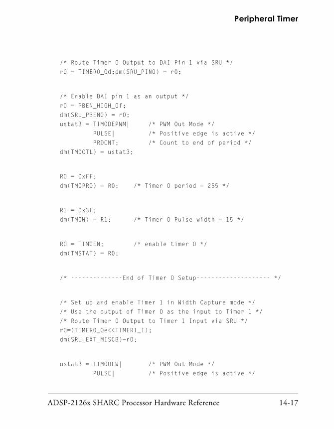
ADSP-2126x SHARC Processor Hardware Reference 14-17
Peripheral Timer
/* Route Timer 0 Output to DAI Pin 1 via SRU */
r0 = TIMER0_Od;dm(SRU_PIN0) = r0;
/* Enable DAI pin 1 as an output */
r0 = PBEN_HIGH_Of;
dm(SRU_PBEN0) = r0;
ustat3 = TIMODEPWM| /* PWM Out Mode */
PULSE| /* Positive edge is active */
PRDCNT; /* Count to end of period */
dm(TM0CTL) = ustat3;
R0 = 0xFF;
dm(TM0PRD) = R0; /* Timer 0 period = 255 */
R1 = 0x3F;
dm(TM0W) = R1; /* Timer 0 Pulse width = 15 */
R0 = TIM0EN; /* enable timer 0 */
dm(TMSTAT) = R0;
/* --------------End of Timer 0 Setup-------------------- */
/* Set up and enable Timer 1 in Width Capture mode */
/* Use the output of Timer 0 as the input to Timer 1 */
/* Route Timer 0 Output to Timer 1 Input via SRU */
r0=(TIMER0_Oe<<TIMER1_I);
dm(SRU_EXT_MISCB)=r0;
ustat3 = TIMODEW| /* PWM Out Mode */
PULSE| /* Positive edge is active */

Timer Programming Examples
14-18 ADSP-2126x SHARC Processor Hardware Reference
IRQEN| /* Enable Timer 1 Interrupt */
PRDCNT; /* Count to end of period */
dm(TM1CTL) = ustat3;
R0 = TIM1EN; /* enable timer 1 */
dm(TMSTAT) = R0;
/* Poll the Timer 1 interrupt latch, the interrupt will latch
when the measured period and pulse width are ready to read */
bit tst LIRPTL GPTMR1I;
if not tf jump(pc,-1);
/* Read the measured values */
r0 = dm(TM1PRD);
r1 = dm(TM1W);
/* r0 and r1 will match the Timer 0 settings above */
_main.end: jump (pc,0);
Listing 14-3. Using a General-Purpose Timer as a Core Timer
/* Register Definitions */#define TMSTAT (0x1400) /* GP Timer
Status Register */
#define TM0CTL (0x1401) /* GP Timer 0 Control Register */
#define TM0PRD (0x1403) /* GP Timer 0 Period Register */
#define TM0W (0x1404) /* GP Timer 0 Width Register */
/* Bit Definitions */#define TIMODEPWM (0x00000001)
#define PRDCNT (0x00000008)
#define IRQEN (0x00000010)
#define TIM0EN (0x00000100)
/* Main code section */
.global _main;
.section/pm seg_pmco;

ADSP-2126x SHARC Processor Hardware Reference 14-19
Peripheral Timer
_main:
/* Using PWM Out mode as a core timer */
ustat3 = TIMODEPWM| /* PWM Out Mode */
PRDCNT| /* Count to end of period */ IRQEN;dm(TM0CTL) = ustat3;
R0 = 0x8000;
dm(TM0PRD) = R0; /* Timer 0 period = 0x8000 */
R1 = 1;
dm(TM0W) = R1; /* Timer 0 Pulse width = 1 */
R0 = TIM0EN; /* enable timer 0 */
dm(TMSTAT) = R0;
/* Get start clock count */
R1 = EMUCLK;
// Wait until TIM0IRQ is set
// Alternatively, we could test GPTMR0I in IRPTL
r0=dm(TMSTAT);
btst r0 by 0;
if not sz jump (pc,2);
jump(pc,-3) (db);
/* Get end clock count */
R2=EMUCLK;
/* Subtract the start count from the end count
to obtain the number of cycles before the interrupt */
R4=R2-R1;
// R4 will be double the value of TM0PRD
_main.end: jump(pc,0);

Timer Programming Examples
14-20 ADSP-2126x SHARC Processor Hardware Reference

ADSP-2126x SHARC Processor Hardware Reference 15-1
15 SYSTEM DESIGN
The processor supports many system design options. The options imple-mented in a system are influenced by cost, performance, and system requirements. This chapter provides the following system design information:
• “Pin Descriptions” on page 15-2
• “Phase-Locked Loop Startup” on page 15-13
• “Conditioning Input Signals” on page 15-14
• “Designing for High Frequency Operation” on page 15-15
• “Booting” on page 15-19
Other chapters also discuss system design issues. Some other locations for system design information include:
• “SPORT Operation Modes” on page 9-9
• “SPI General Operations” on page 10-7
By following the guidelines described in this chapter, you can ease the design process for your ADSP-2126x product. Development and testing of your application code and hardware can begin without debugging the debug port.

Pin Descriptions
15-2 ADSP-2126x SHARC Processor Hardware Reference
Pin DescriptionsThe processor’s pin descriptions are fully described in the ADSP-2126x SHARC Processor Data Sheet.
Pin MultiplexingThe ADSP-2126x provides the same functionality as other SHARC pro-cessors but with a much lower pin count which helps to reduce total system costs. It does this through extensive use of pin multiplexing. Table 15-2 shows an example multiplexing scheme. The following regis-ters (addresses) and bits are used.
Table 15-1. Register and their Bits Used for Multiplexing
Registers Used (Address) Bits Used
SYSCTL (0x3024) PPFLGS, TMREXPEN, IRQxEN
SPIFLG (0x1001) SPIFLGx (3:0)
SPICTL (0x1000) SPIMS
IDP_PDAP_CTL (0x24B1)
IDP_PP_SELECT
PMCTL (0x2000) CLOCKOUTEN (for debug only)

ADSP-2126x SHARC Processor Hardware Reference 15-3
System Design
Table 15-2. ADSP-2126x Processor Pin Multiplexing Scheme
External Pin Function TypeI = inputO = output
Control0 = cleared1 = setx = do not care
FLGn1 FLGn I/O PPFLGS = 0SPIFLG[n] = 0 and SPIMS=0IRQxEN = 0
IRQn2 I PPFLGS=0SPIFLG[n] = 0 and SPIMS = 0IRQxEN = 1
SPI Device Select3 O PPFLGS=0SPIFLG[n] = 1 and SPIMS = 1IRQxEN = 0
AD[15:0] AD[15:0] I/O PPFLGS = 04
IDP_PP_SELECT = 0
PDAP I PPFLGS = 0IDP_PP_SELECT = 1
FLG[15:0] I/O PPFLGS = 15
IDP_PP_SELECT = 0
DAI_P[20:1]6 PDAP I IDP_PP_SELECT = 0
FLG[15:10] I/O Note7
Other I/O Note 6
CLKOUT CLKOUT O PMCTL [12] = 1 (for debug only)
RESETOUT O PMCTL [12] = 0
1 n = 0, 1, 2, 3.2 For n = 3 function is FLG3 or TIMEXP, not IRQ3.3 These pins are used at boot time as device selects during SPI Master booting.4 Setting PPFLGS = 1 and IDP_PP_SELECT = 1 at the same time is illegal.5 When PPFLGS = 1, the FLG pins toggle then alternate functions. For example IRQx and
TIMEXP.6 For complete information on the operation of these pins, see “Digital Audio Interface” on
page 12-1.7 For complete information on the operation of these pins, see “Clock Routing Control Reg-
isters (SRU_CLKx, Group A)” on page A-112.

Pin Descriptions
15-4 ADSP-2126x SHARC Processor Hardware Reference
If the system clock to the SPICLK module is shut off in the PMCTL register, FLG0–3 are not usable.
Input Synchronization DelayThe processor has several asynchronous inputs—RESET, TRST, IRQ2–0, DAI pins and FLG15-0 (when configured as inputs). These inputs can be asserted in arbitrary phase to the processor clock, CLKIN. The processor synchronizes the inputs prior to recognizing them. The delay associated with recognition is called the synchronization delay.
Any asynchronous input must be valid prior to the recognition point in a particular cycle. If an input does not meet the setup time on a given cycle, it may be recognized in the current cycle or during the next cycle.
To ensure recognition of an asynchronous input, it must be asserted for at least one full processor cycle plus setup and hold time, except for RESET, which must be asserted for at least four processor cycles. The minimum time prior to recognition (the setup and hold time) is specified in the data sheet.
Clock DerivationThe processor uses a PLL on the chip, to provide clocks that switch at higher frequencies than the system clock (CLKIN). The PLL-based clocking methodology used influences the clock frequencies and behavior for the serial, SPI, and parallel ports, in addition to the processor core and inter-nal memory. In each case, the processor PLL provides a non-skewed clock to the port logic and I/O pins.
The PLL provides a clock that switches at the processor core frequency to the serial ports. Each of the serial ports can be programmed to operate at clock frequencies derived from this clock. The six serial ports’ transmit and receive clocks are divided down from the processor core clock fre-quency by setting the DIVx registers appropriately.

ADSP-2126x SHARC Processor Hardware Reference 15-5
System Design
On power-up, the CLKCFG1–0 pins are used to select ratios of 16:1, 8:1, and 3:1. After booting, numerous other ratios (slowing or speeding up the clock) can be selected via software control using the Power Management Control register.
Power Management Control Register
The ADSP-2126x has a Power Management Control register (PMCTL) that allows programs to determine the amount of power dissipated. This includes the ability to program the PLL dynamically in software. This fea-ture eases design for systems that need to use specific clock frequencies or are sensitive to power consumption.
In addition to changing the clock rate on the fly, The PMCTL register also allows programs to disable the clock source to a particular processor peripheral completely, (for example the serial ports or the timers), to fur-ther conserve power. By default, each peripheral block has its internal CLK enabled only after it is initialized. Programs can use the PMCTL register to turn the specific peripheral off after the application no longer needs it. After reset these clocks are not enabled until the peripheral is initialized by the program.
Listing 15-1 and Listing 15-2 are examples that show how to use the Power Management Control register to enable/disable clocking to a peripheral.
Listing 15-1. Power Management Example
ustat2 = dm(PMCTL);
bit set ustat2 SPIPDN; /* disable internal peripheral clock for
SPI module. SPIPDN is defined as bit 3
of PMCTL*/ dm(PMCTL) = ustat2;

Pin Descriptions
15-6 ADSP-2126x SHARC Processor Hardware Reference
Listing 15-2. PMCTL Example Code.
PLL Divisor modification:
ustat2 = dm(PMCTL); bit set ustat2 DIVEN|PLLD8; /* set and enable PLL Divisor for CoreCLK = CLKIN/8 */
dm(PMCTL) = ustat2;
PLL Multiplier modification:
ustat2 = dm(PMCTL); bit set ustat2 PLLM8 | PLLBP; /* set a multiplier of 8 (default divisor is 2) and put
PLL in Bypass */
dm(PMCTL) = ustat2; waiting loop: r0 = 4096; /* wait for PLL to lock at new rate (requirement for modifying multiplier only) */
lcntr = r0, do pllwait until lce; pllwait:nop; ustat2 = dm(PMCTL); bit clr ustat2 PLLBP; /* take PLL out of Bypass, PLL is now at CLKIN*4 (CoreCLK = CLKIN
* M/N = CLKIN* 8/2) */
dm(PMCTL) = ustat2;
PLL Input Divider Usage:
ustat2 = dm(PMCTL);
bit set ustat2 INDIV | PLLBP; /* divide clkin/2, put
PLL in Bypass */
dm(PMCTL) = ustat2;
waiting loop:

ADSP-2126x SHARC Processor Hardware Reference 15-7
System Design
r0 = 4096; /* wait for PLL to lock at new rate
(requirement for modifying multiplier
and setting INDIV bit only) */
lcntr = r0, do pllwait until lce;
pllwait:nop;
ustat2 = dm(PMCTL);
bit clr ustat2 PLLBP;
/* take PLL out of Bypass */
dm(PMCTL) = ustat2;
PMCTL register bit definitions:
/* Power Management Control register (PMCTL) */
#define PLLM8 (BIT_3) // PLL Multiplier 8
#define PLLD8 (BIT_7) // PLL Divisor 8
#define INDIV (BIT_8) // Input Divider
#define DIVEN (BIT_9) // Enable PLL Divisor
#define CLKOUTEN (BIT_12) // Mux select for CLKOUT/RESETOUT
#define PLLBP (BIT_15) // PLL Bypass mode indication
#define SPIPDN (BIT_30) // Shutdown clock to SPI
RESET and CLKINThe processor receives its clock input on the CLKIN pin. The processor uses an on-chip phase-locked loop (PLL) to generate its internal clock, which is a multiple of the CLKIN frequency (Figure 15-1 on page 15-11). Because the PLL requires some time to achieve phase lock, CLKIN must be valid for a minimum time period during reset before the RESET signal can be deas-serted. For information on minimum clock setup, see the specific ADSP-2126x data sheet.
Table 15-3 and Table 15-4 show the internal clock to CLKIN frequency ratios supported by the processor. Note that programs control the PLL through the PMCTL register. This register is described in “Power Manage-ment Registers” on page A-64.
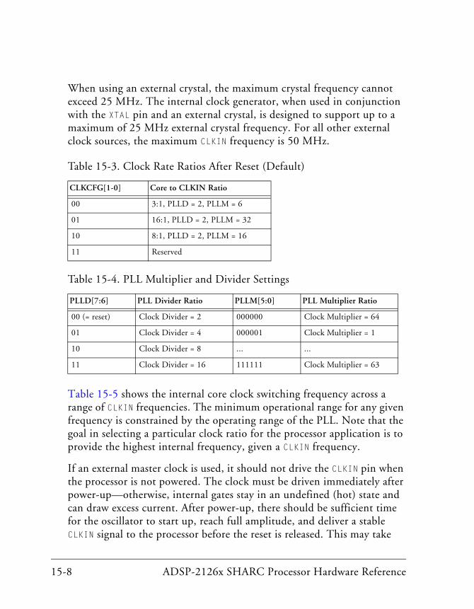
15-8 ADSP-2126x SHARC Processor Hardware Reference
When using an external crystal, the maximum crystal frequency cannot exceed 25 MHz. The internal clock generator, when used in conjunction with the XTAL pin and an external crystal, is designed to support up to a maximum of 25 MHz external crystal frequency. For all other external clock sources, the maximum CLKIN frequency is 50 MHz.
Table 15-5 shows the internal core clock switching frequency across a range of CLKIN frequencies. The minimum operational range for any given frequency is constrained by the operating range of the PLL. Note that the goal in selecting a particular clock ratio for the processor application is to provide the highest internal frequency, given a CLKIN frequency.
If an external master clock is used, it should not drive the CLKIN pin when the processor is not powered. The clock must be driven immediately after power-up—otherwise, internal gates stay in an undefined (hot) state and can draw excess current. After power-up, there should be sufficient time for the oscillator to start up, reach full amplitude, and deliver a stable CLKIN signal to the processor before the reset is released. This may take
Table 15-3. Clock Rate Ratios After Reset (Default)
CLKCFG[1-0] Core to CLKIN Ratio
00 3:1, PLLD = 2, PLLM = 6
01 16:1, PLLD = 2, PLLM = 32
10 8:1, PLLD = 2, PLLM = 16
11 Reserved
Table 15-4. PLL Multiplier and Divider Settings
PLLD[7:6] PLL Divider Ratio PLLM[5:0] PLL Multiplier Ratio
00 (= reset) Clock Divider = 2 000000 Clock Multiplier = 64
01 Clock Divider = 4 000001 Clock Multiplier = 1
10 Clock Divider = 8 ... ...
11 Clock Divider = 16 111111 Clock Multiplier = 63

ADSP-2126x SHARC Processor Hardware Reference 15-9
System Design
100 μs depending on the choice of crystal, operating frequency, loop gain and capacitor ratios. For details on timing, refer to the product specific data sheet.
After the external processor RESET signal is deasserted, the PLL starts oper-ating. The rest of the chip will be held in reset for 4096 CLKIN cycles after RESET is deasserted by an internal reset signal. This sequence allows the PLL to lock and stabilize. Add one CLKIN cycle if RESET doesn’t meet setup requirements with respect to the CLKIN falling edge.
Reset GeneratorsIt is important that a processor (or programmable device) have a reliable active RESET that is released once the power supplies and internal clock cir-cuits have stabilized. The RESET signal should not only offer a suitable delay, but it should also have a clean monotonic edge. Analog Devices has a range of microprocessor supervisory ICs with different features. Features include one or more of the following:
• Power-up reset
• Optional manual reset input
Table 15-5. Selecting Core to CLKIN Ratio
Typical Crystal and Clock Oscillators Inputs
12.5 16.67 25 33.3 40 50
Clock Ratios Core CLK (MHz)
3:1 37.5 50 75 100 120 150
8:1 100 133.36 200 N/A N/A N/A
16:1 200 N/A N/A N/A N/A N/A

15-10 ADSP-2126x SHARC Processor Hardware Reference
• Power low monitor
• Backup battery switching
The part number series for supervisory circuits from Analog Devices are:
• ADM69x
• ADM70x
• ADM80x
• ADM1232
• ADM181x
• ADM869x
A simple power-up reset circuit is shown below, using the ADM809-RART reset generator. The ADM809 provides an active low RESET signal whenever the supply voltage is below 2.63 V. At power-up, a 240 ms active reset delay is generated to give the power supplies and oscil-lators time to stabilize.
Another part, the ADM706TAR, provides power on RESET and optional manual RESET. It allows designers to create a more complete supervisory circuit that monitors the supply voltage. Monitoring the supply voltage allows the system to initiate an orderly shutdown in the event of power failure. The ADM706TAR also allows designers to create a watchdog timer that monitors for software failure. This part is available in an eight-lead SOIC package. Figure 15-2 shows a typical application circuit using the ADM706TAR.
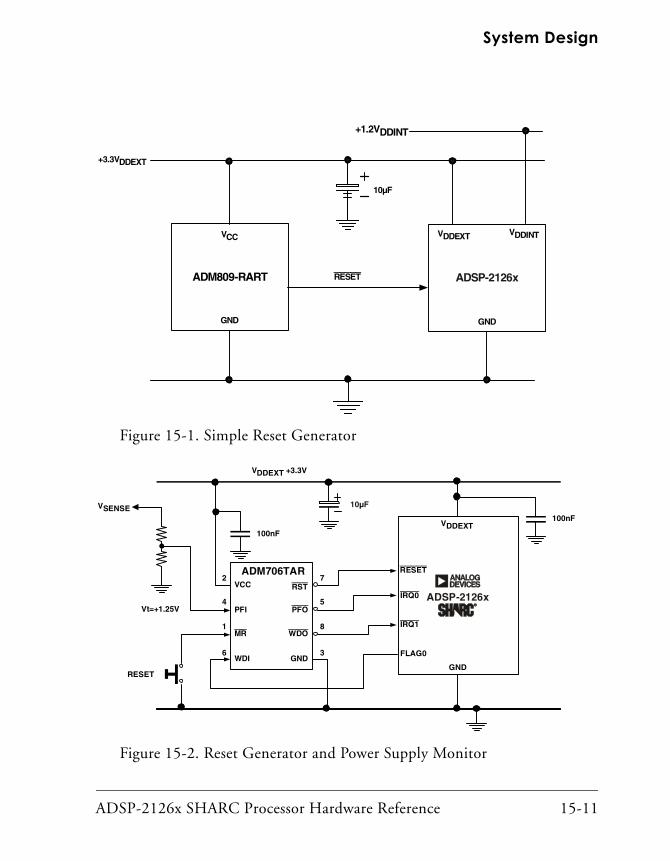
ADSP-2126x SHARC Processor Hardware Reference 15-11
System Design
Figure 15-1. Simple Reset Generator
Figure 15-2. Reset Generator and Power Supply Monitor
VCC
GND
ADM809-RART
VDDEXT
RESET
GND
+3.3VDDEXT
10µF
VDDINT
+1.2VDDINT
ADSP-2126x
RESET
IRQ0
IRQ1
FLAG0
GNDRESET
Vt=+1.25V
VSENSE
VDDEXT
PFI
MR
WDI
PFO
WDO
GND
4
1
6
5
8
3
ADM706TARVCC
2RST
7
100nF
10µF
100nF
VDDEXT +3.3V
aADSP-2126xS

Pin Descriptions
15-12 ADSP-2126x SHARC Processor Hardware Reference
Interrupt and Peripheral Timer PinsThe processor’s external interrupt pins, flag pins, and timer pin can be used to send and receive control signals to and from other devices in the system. Hardware interrupt signals IRQ2–0 are received on the FLG2–0 pins and the TIMEXP pin is mapped on the FLG3 pin. Hardware interrupt signals (IRQ2–0) are received on the FLG2–0 pins. Interrupts can come from devices that require the processor to perform some task on demand. A memory-mapped peripheral, for example, can use an interrupt to alert the processor that it has data available.
The TIMEXP output is generated by the on-chip timer. It indicates to other devices that the programmed time period has expired.
Core-Based Flag PinsThe FLG3–0 pins allow single bit signalling between the processor and other devices. For example, the processor can raise an output flag to inter-rupt a host processor. Each flag pin can be programmed to be either an input or output. In addition, many instructions can be conditioned on a flag’s input value, enabling efficient communication and synchronization between multiple processors or other interfaces.
The flags are bidirectional pins and all have the same functionality. The FLGxO bits in the FLAGS register program the direction of each flag pin.
JTAG Interface PinsThe JTAG Test Access Port (TAP) consists of the TCK, TMS, TDI, TDO, and TRST pins. The JTAG port can be connected to a controller that performs a boundary scan for testing purposes. This port is also used by the Analog Devices Tools product line of JTAG emulator and development software to access on-chip emulation features. To allow the use of the emulator, a connector for its in-circuit probe must be included in the target system.

ADSP-2126x SHARC Processor Hardware Reference 15-13
System Design
If the TRST pin is not asserted (or held low) at power-up, the JTAG port is in an undefined state that may cause the processor to drive out on I/O pins that would normally be three-stated at reset. The TRST pin can be held low with a jumper to ground on the target board connector.
A detailed discussion of JTAG and its use can be found in the Engi-neer-to-Engineer Note (EE-68), Analog Devices JTAG Emulation Technical Reference. This document is available on the Analog Devices Web site at www.analog.com.
Phase-Locked Loop StartupThe RESET signal can be held low long enough to guarantee a stable CLKIN source and stable VDDINT/VDDEXT power supplies before the PLL is reset.
In order for the PLL to lock to the CLKIN frequency, the PLL needs time to lock before the core can execute or begin the boot process. A delayed core reset has been added via the delay circuit. There is a 12-bit counter that
Figure 15-3. Chip Reset Circuit
CLKIN
RESET
Delayed Internal Core Processor
PLLCore Reset Delay Circuit
CLKIN CORE_RST
CLKIN
ENA_CLK
PLL_RESET
12-bit Counter Count 4096 CLKIN Cycles
ENA_CNT
RESETOUT
PLL reset and PLL clock input enable occur on the
rising edge of RESET
Reset

Conditioning Input Signals
15-14 ADSP-2126x SHARC Processor Hardware Reference
counts up to 4096 CLKIN cycles after RESET is transitioned from low to high. The delay circuit is activated at the same time the PLL is taken out of reset.
The advantage of the delayed core reset is that the PLL can be reset any number of times without having to power-down the system. If there is a brown-out situation, the watchdog circuit only has to control the RESET.
Conditioning Input SignalsThe processor is a CMOS device. It has input conditioning circuits which simplify system design by filtering or latching input signals to reduce sus-ceptibility to glitches or reflections.
The following sections describe why these circuits are needed and their effect on input signals.
A typical CMOS input consists of an inverter with specific N and P device sizes that cause a switching point of approximately 1.4 V. This level is selected to be the midpoint of the standard TTL interface specification of VIL = 0.8 V and VIH = 2.0 V. This input inverter, unfortunately, has a fast response to input signals and external glitches wider than 1 ns. Filter cir-cuits and hysteresis are added after the input inverter on some processor inputs, as described in the following sections.
Input Pin HysteresisHysteresis (shown in Figure 15-4) is used on all SHARC input signals. Hysteresis causes the switching point of the input inverter to be slightly above 1.4 V (VT) for a rising edge (VT+) and slightly below 1.4 V for a falling edge (VT–). The value of the hysteresis is approximately ± 100 mV. The hysteresis is intended to prevent multiple triggering of signals that are allowed to rise slowly, as might be expected for example on a reset line with a delay implemented by an RC input circuit. Hysteresis is not used to
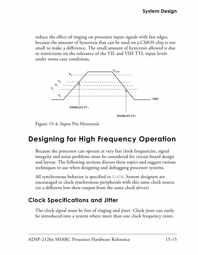
ADSP-2126x SHARC Processor Hardware Reference 15-15
System Design
reduce the effect of ringing on processor input signals with fast edges, because the amount of hysteresis that can be used on a CMOS chip is too small to make a difference. The small amount of hysteresis allowed is due to restrictions on the tolerance of the VIL and VIH TTL input levels under worst-case conditions.
Designing for High Frequency OperationBecause the processor can operate at very fast clock frequencies, signal integrity and noise problems must be considered for circuit board design and layout. The following sections discuss these topics and suggest various techniques to use when designing and debugging processor systems.
All synchronous behavior is specified to CLKIN. System designers are encouraged to clock synchronous peripherals with this same clock source (or a different low-skew output from the same clock driver).
Clock Specifications and JitterThe clock signal must be free of ringing and jitter. Clock jitter can easily be introduced into a system where more than one clock frequency exists.
Figure 15-4. Input Pin Hysteresis
GNDVIL
VIH
VDDEXT
VTVT-
VT+
ENABLES VT-
ENABLES VT+

Designing for High Frequency Operation
15-16 ADSP-2126x SHARC Processor Hardware Reference
Jitter should be kept to an absolute minimum. High frequency jitter on the clock to the processor may result in abbreviated internal cycles.
Never share a clock buffer IC with a signal of a different clock fre-quency. This introduces excessive jitter.
As shown in Figure 15-5, keep the portions of the system that operate at different frequencies as physically separate as possible. The clock supplied to the processor must have a rise time of 3 ns or less and must meet or exceed a high and low voltage of 2 V and 0.4 V, respectively.
Other Recommendations and Suggestions• Use more than one ground plane on the PCB to reduce crosstalk.
Be sure to use lots of vias between the ground planes. One VDD plane for each supply is sufficient. These planes should be in the center of the PCB.
• To reduce crosstalk, keep critical signals such as clocks, strobes, and bus requests on a signal layer next to a ground plane and away from or layout perpendicular to other non-critical signals.
• If possible, position the processors on both sides of the board to reduce area and distances.
• To allow better control of impedance and delay, and to reduce crosstalk, design for lower transmission line impedances.
Figure 15-5. Reducing Clock Jitter and Ring
FREQUENCY 1 CLOCK aADSP-2126x
S

ADSP-2126x SHARC Processor Hardware Reference 15-17
System Design
• Use 3.3 V peripheral components and power supplies to help reduce transmission line problems, ground bounce and noise cou-pling (the receiver switching voltage of 1.5 V is close to the middle of the voltage swing).
• Experiment with the board and isolate crosstalk and noise issues from reflection issues. This can be done by driving a signal wire from a pulse generator and studying the reflections while other components and signals are passive.
Decoupling Capacitors and Ground PlanesGround planes must be used for the ground and power supplies. Designs should use a minimum of eight bypass capacitors (six 0.1 μF and two 0.01 μF ceramic). The capacitors should be placed very close to the VDDEXT and VDDINT pins of the package as shown in Figure 15-6. Use short and fat traces for this. The ground end of the capacitors should be tied directly to the ground plane inside the package footprint of the processor (under-neath, on the bottom of the board), not outside the footprint. A surface-mount capacitor is recommended because of its lower series induc-tance. Connect the power plane to the power supply pins directly with minimum trace length. The ground planes must not be densely perforated with vias or traces as their effectiveness is reduced. In addition, there should be several large tantalum capacitors on the board.
Designs can use either bypass placement case shown in Figure 15-6, or combinations of the two. Designs should try to minimize signal feedthroughs that perforate the ground plane.
Oscilloscope ProbesWhen making high speed measurements, be sure to use a “bayonet” type or similarly short (< 0.5 inch) ground clip, attached to the tip of the oscil-loscope probe. The probe should be a low capacitance active probe with 3 pF or less of loading. The use of a standard ground clip with four

Designing for High Frequency Operation
15-18 ADSP-2126x SHARC Processor Hardware Reference
inches of ground lead causes ringing to be seen on the displayed trace and makes the signal appear to have excessive overshoot and undershoot. A 1 GHz or better sampling oscilloscope is needed to see the signals accurately.
Recommended ReadingThe text High-Speed Digital Design: A Handbook of Black Magic is recom-mended for further reading. This book is a technical reference that covers the problems encountered in state-of-the-art, high frequency digital cir-
Figure 15-6. Bypass Capacitor Placement
CASE 1:BYPASS CAPACITORS ON NON-COMPONENT(BOTTOM) SIDE OF BOARD, BENEATH DSP PACKAGE
aADSP-21262
S
CASE 2:BYPASS CAPACITORS ON COMPONENT (TOP)SIDE OF BOARD, AROUND DSP PACKAGE

ADSP-2126x SHARC Processor Hardware Reference 15-19
System Design
cuit design. It is also an excellent source of information and practical ideas. Topics covered in the book include:
• High-Speed Properties of Logic Gates
• Measurement Techniques
• Transmission Lines
• Ground Planes and Layer Stacking
• Terminations
• Vias
• Power Systems
• Connectors
• Ribbon Cables
• Clock Distribution
• Clock Oscillators
High-Speed Digital Design: A Handbook of Black Magic, Johnson & Gra-ham, Prentice Hall, Inc., ISBN 0-13-395724-1.
BootingWhen a processor is initially powered up, its internal SRAM is undefined. Before actual program execution can begin, the application must be loaded from an external non-volatile source such as flash memory or a host processor. This process is known as bootstrap loading or booting and is automatically performed by the ADSP-2126x processor after power-up or after a software reset.

Booting
15-20 ADSP-2126x SHARC Processor Hardware Reference
The ADSP-2126x supports three booting modes—EPROM, SPI master and SPI slave. Each of these modes uses the following general procedure:
1. At reset, the ADSP-2126x is hardwired to load two hundred fifty-six 32-bit instruction words via a DMA starting at location 0x80000. In this chapter, these instructions are referred to as the boot kernel or loader kernel.
2. The DMA completes and the interrupt associated with the periph-eral that the processor is booting from is activated. The processor jumps to the applicable interrupt vector location (0x80030 for SPI and 0x80050 for the parallel port) and executes the code located there. (Typically, the first instruction at the interrupt vector is a Return From Interrupt (RTI) instruction.)
3. The loader kernel executes a series of Direct Memory Accesses (DMAs) to import the rest of the application, overwriting itself with the applications’ Interrupt Vector Table (IVT).
4. After executing the kernel, the processor returns to location 0x80005 where normal program execution begins.
To support this process, a 256-word loader kernel and loader (which con-verts executables into boot-loader images) are supplied with the VisualDSP++ development tools for both SPI and parallel port booting. For more information on the loader, see the tools documentation in “Product Information” on page -xxxvii.
The boot source is determined by strapping the two BOOTCFGx pins to either logic low or logic high. These settings are shown in Table 15-6.
Table 15-6. Booting Modes
BOOT_CFG1-0 Description
00 SPI Slave boot
01 SPI Master boot

ADSP-2126x SHARC Processor Hardware Reference 15-21
System Design
Parallel Port BootingThe ADSP-2126x supports an 8-bit boot mode through the parallel port. This mode is used to boot from external 8-bit wide memory devices. The processor is configured for 8-bit boot mode when the BOOT_CFG1–0 pins = 10. When configured for parallel boot loading, the parallel port transfers occur with the default bit settings (shown in Table 15-7) for the PPCTL register.
For a complete description of the Parallel Port Control register, see “Paral-lel Port Control Register (PPCTL)” on page A-107.
10 EPROM boot via parallel port
11 ROM Boot mode (not available on all ADSP-2126x processors)
Table 15-7. Parallel Port Boot Mode Settings in the PPCTL Register
Bit Setting
PPALEPL = 0; ALE is active high
PPEN = 1
PPDUR = 10111; (24 core clock cycles per data transfer cycle)
PPBHC = 1; insert a bus hold cycle on every access
PP16 = 0; external data width = 8 bits
PPDEN = 1; use DMA
PPTRAN = 0; receive (read) DMA
PPBHD = 0; buffer hang enabled
Table 15-6. Booting Modes
BOOT_CFG1-0 Description

Booting
15-22 ADSP-2126x SHARC Processor Hardware Reference
The parallel port DMA channel is used when downloading the boot kernel information to the processor. At reset, the DMA Parameter registers are initialized to the values listed in Table 15-8.
Unlike previous SHARC processors, the ADSP-2126x does not have a Boot Memory Select (BMS) pin.
SPI Port BootingThe ADSP-2126x supports booting from a host processor via SPI Slave mode (BOOT_CFG1–0 = 00), and booting from an SPI Flash, SPI PROM, or a host processor via SPI Master mode (BOOT_CFG1–0 = 01).
In both (master and slave) boot modes, the LSBF format is used and SPI mode 3 is selected (clock polarity and clock phase = 1).
Both SPI boot modes support booting from 8-, 16-, or 32-bit SPI devices. In all SPI boot mode, the data word size in the shift register is hardwired to 32 bits. Therefore, for 8 or 16-bit devices, data words are packed into the Shift register to generate 32-bit words least significant bit (LSB) first, which are then shifted into internal memory. The relationship between
Table 15-8. Parameter Initialization Value
Parameter Register Initialization Value Comment
PPCTL 0x0000 016F See Table 15-7.
IIPP 0 This is the offset from internal memory normal word starting address of 0x80000.
ICPP 0x180 (384) This is the number of 32-bit words that are equivalent to 256 instructions.
IMPP 0x01
EIPP 0x00
ECPP 0x600 This is the number of bytes in 0x100 48-bit instructions.
EMPP 0x01

ADSP-2126x SHARC Processor Hardware Reference 15-23
System Design
the 32-bit words received into the RXSPI register and the instructions that need to be placed in internal memory is shown in Figure 15-7.
For more information about 32- and 48-bit internal memory addressing, see “Setting Data Access Modes” on page 5-27.
For 16-bit SPI devices, two words shift into the 32-bit receive Shift regis-ter (RXSR) before a DMA transfer to internal memory occurs. For 8-bit SPI devices, four words shift into the 32-bit receive shift register before a DMA transfer to internal memory occurs.
When booting, the ADSP-2126x processor expects to receive words into the RXSPI register seamlessly. This means that bits are received continu-ously without breaks. For more information, see “Core Transmit and Receive Operations” on page 10-12. For different SPI host sizes, the pro-cessor expects to receive instructions and data packed in a least significant word (LSW) format.
Figure 15-7. SPI Data Packing
32-BIT RECEIVESHIFT
REGISTER
S
DMA #1: DM[80000]
MSW LSW
4 3 2 1
PM48 [0X800FF]
16
DMA #2: DM[80001]
MSW LSW
DMA #3: DM[40002]
MSW LSW
PM48 [0X80003]
DMA #6: DM[80005]
MSW LSW
MOSI
256 48-BITWORDS
0X800FF
0X80000
DMA #4: DM[80003]
MSW LSW
PM48 [0X80002]
DMA
P
I
R
X PM48 [0X80001]
DMA #5: DM[80004]
MSW LSW
PM48 [0X80000]
#384:DM[0X8017F]
MSW LSW
#384:DM[0X8017E]
MSW LSW
[X80001]
[X800FE]
[X80002]
LWUW

Booting
15-24 ADSP-2126x SHARC Processor Hardware Reference
Figure 15-8 shows how a pair of instructions are packed for SPI booting using a 32-, 16-, and an 8-bit device. These two instructions are received as three 32-bit words as illustrated in Figure 15-7.
The following sections examine how data is packed into internal memory during SPI booting for SPI devices with widths of 32, 16, or 8 bits.
32-bit SPI Host Boot
Figure 15-9 shows 32-bit SPI host packing of 48-bit instructions executed at PM addresses 0x80000 and 0x80001. The 32-bit word is shifted to internal program memory during the 256-word kernel load.
The following example shows a 48-bit instructions executed:[0x80000] 0x112233445566
[0x80001] 0x7788AABBCCDD
Figure 15-8. Instruction Packing for Different Hosts
16-BIT HOST
CCDD1122
1122
33445566 7788AABB
CCDD AABB 778833445566
66 55 44 33 22 11 DD CC BB AA 88 77
32-BIT HOST
8-BIT HOST
[0x80000] 0x1122 33445566
[0x80001] 0x7788 AABBCCDD
WORDSINSTRUCTIONS IN
INTERNAL MEMORY
t = 0 t = 96 SPICLK

ADSP-2126x SHARC Processor Hardware Reference 15-25
System Design
The 32-bit SPI host packs or prearranges the data as:
SPI word 1= 0x33445566
SPI word 2 = 0xCCDD1122
SPI word 3 = 0x7788AABB
16-bit SPI Host Boot
Figure 15-10 shows how a 16-bit SPI host packs 48-bit instructions at PM addresses 0x80000 and 0x80001. For 16-bit hosts, two 16-bit words are packed into the shift register to generate a 32-bit word. The 32-bit word shifts to internal program memory during the kernel load.
The following example shows a 48-bit instructions executed.[0x80000] 0x112233445566
[0x80001] 0x7788AABBCCDD
Figure 15-9. 32-Bit SPI Host Packing
RXSPI DMA INTERNALMEMORY
0x90000
0x900FF
MOSI
32 3232
32-B
ITW
OR
DN

Booting
15-26 ADSP-2126x SHARC Processor Hardware Reference
The 16-bit SPI host packs or prearranges the data as:
SPI word 1 = 0x5566SPI word 2 = 0x3344
SPI word 3 = 0x1122SPI word 4 = 0xCCDD
SPI word 5 = 0xAABBSPI word 6 = 0x7788
The initial boot of the 256-word loader kernel requires a 16-bit host to transmit 768 16-bit words. Two packed 16-bit words comprise the 32-bit word. The SPI DMA count value of 0x180 is equivalent to 384 words. Therefore, the total number of 16-bit words loaded is 768.
8-bit SPI Host Boot
Figure 15-11 shows 8-bit SPI host packing of 48-bit instructions executed at PM addresses 0x80000 and 0x80001. For 8-bit hosts, four 8-bit words pack into the shift register to generate a 32-bit word. The 32-bit word
Figure 15-10. 16-Bit SPI Host Packing
WO
RD
N
16-
BIT
WO
RD
N+
1
RXSPI DMAINTERNALMEMORY
(LOADER KERNEL)
0X80000
0X800FF
MOSI
32 3232
16-
BIT

ADSP-2126x SHARC Processor Hardware Reference 15-27
System Design
shifts to internal program memory during the load of the 256-instruction word kernel.
The following example shows a 48-bit instructions executed.[0x80000] 0x112233445566
[0x80001] 0x7788AABBCCDD
The 8-bit SPI host packs or prearranges the data as:
SPI word 1 = 0x66SPI word 2 = 0x55
SPI word 3 = 0x44SPI word 4 = 0x33
SPI word 5 = 0x22SPI word 6 = 0x11
SPI word 7 = 0xDDSPI word 8 = 0xCC
Figure 15-11. 8-Bit SPI Host Packing
RXSPI
DMA
MOSI
0X80000
0X800FF
32 3232
8-B
ITW
OR
DN
+1
8-B
ITW
OR
DN
8-B
ITW
OR
DN
+2
8-B
ITW
OR
DN
+3
INTERNALMEMORY
LOADER KERNEL

Booting
15-28 ADSP-2126x SHARC Processor Hardware Reference
SPI word 9 = 0xBBSPI word 10 = 0xAA
SPI word 11 = 0x88SPI word 12 = 0x77
The initial boot of the 256-word loader kernel requires an 8-bit host to transmit fifteen hundred thirty-six 8-bit words. The SPI DMA count value of 0x180 is equal to 384 words. Since one 32-bit word is created from four packed 8-bit words, the total number of 8-bit words transmitted is 1536.
For all boot modes, the VisualDSP++ loader automatically outputs the correct word width and count based on the project settings. For more information, see the VisualDSP++ tools documentation.
Slave Boot Mode
In Slave boot mode, the host processor initiates the booting operation by activating the SPICLK signal and asserting the SPIDS signal to the active low state. The 256-word kernel is loaded 32 bits at a time, via the SPI Receive Shift register (RXSR). To receive 256 instructions (48-bit words) properly, the SPI DMA initially loads a DMA count of 0x180 (384) 32-bit words, which is equivalent to 0x100 (256) 48-bit words.
The processor’s SPIDS pin should not be tied low. When in SPI Slave mode, including booting, the SPIDS signal is required to tran-sition from high to low. SPI slave booting uses the default bit settings shown in Table 15-9.
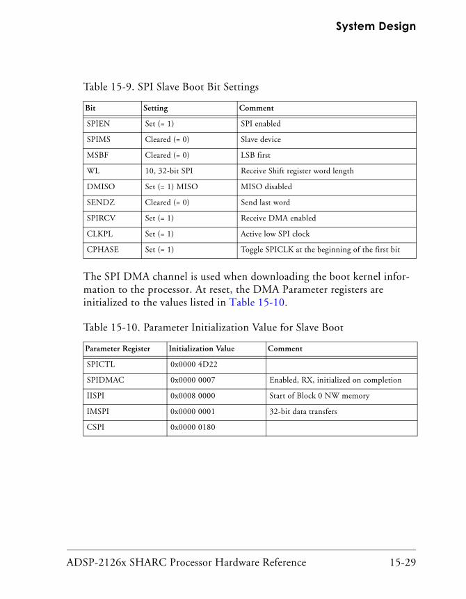
ADSP-2126x SHARC Processor Hardware Reference 15-29
System Design
The SPI DMA channel is used when downloading the boot kernel infor-mation to the processor. At reset, the DMA Parameter registers are initialized to the values listed in Table 15-10.
Table 15-9. SPI Slave Boot Bit Settings
Bit Setting Comment
SPIEN Set (= 1) SPI enabled
SPIMS Cleared (= 0) Slave device
MSBF Cleared (= 0) LSB first
WL 10, 32-bit SPI Receive Shift register word length
DMISO Set (= 1) MISO MISO disabled
SENDZ Cleared (= 0) Send last word
SPIRCV Set (= 1) Receive DMA enabled
CLKPL Set (= 1) Active low SPI clock
CPHASE Set (= 1) Toggle SPICLK at the beginning of the first bit
Table 15-10. Parameter Initialization Value for Slave Boot
Parameter Register Initialization Value Comment
SPICTL 0x0000 4D22
SPIDMAC 0x0000 0007 Enabled, RX, initialized on completion
IISPI 0x0008 0000 Start of Block 0 NW memory
IMSPI 0x0000 0001 32-bit data transfers
CSPI 0x0000 0180

Booting
15-30 ADSP-2126x SHARC Processor Hardware Reference
Master Boot
In Master Boot mode, the ADSP-2126x initiates the booting operation by:
1. Activating the SPICLK signal and asserting the FLG0 signal to the active low state.
2. Writing the read command 0x03 and address 0x00 to the slave device as shown in Figure 15-8.
Master Boot mode is used when the processor is booting from an SPI compatible serial PROM, serial FLASH, or slave host processor. The spe-cifics of booting from these devices are discussed individually. On reset, the interface starts up in Master mode performing a three hundred eighty-four 32-bit word DMA transfer.
SPI master booting uses the default bit settings shown in Table 15-11.
Table 15-11. SPI Master Boot Mode Bit Settings
Bit Setting Comment
SPIEN Set (= 1) SPI Enabled
SPIMS Set (= 1) Master device
MSBF Cleared (= 0) LSB first
WL 10 32-bit SPI Receive Shift register word length
DMISO Cleared (= 0) MISO enabled
SENDZ Set (= 1) Send zeros
SPIRCV Set (= 1) Receive DMA enabled
CLKPL Set (= 1) Active low SPI clock
CPHASE Set (= 1) Toggle SPICLK at the beginning of the first bit

ADSP-2126x SHARC Processor Hardware Reference 15-31
System Design
The SPI DMA channel is used when downloading the boot kernel infor-mation to the processor. At reset, the DMA parameter registers are initialized to the values listed in Table 15-12.
From the perspective of the ADSP-2126x processor, there is no difference between booting from the three types of SPI slave devices. Since SPI is a full-duplex protocol, the processor is receiving the same amount of bits that it sends as a read command. The read command comprises a full 32-bit word (which is what the processor is initialized to send) comprised of a 24-bit address with an 8-bit opcode. The 32-bit word that is received while this read command is transmitted is thrown away in hardware, and can never be recovered by the user. Because of this, special measures must be taken to guarantee that the boot stream is identical in all three cases. The processor boots in Least Significant Bit First (LSBF) format, while most serial memory devices operate in Most Significant Bit First (MSBF) format. Therefore, it is necessary to program the device in a fashion that is compatible with the required LSBF format.
Also, because the processor always transmits 32 bits before it begins read-ing boot data from the slave device, it is necessary for the VisualDSP++ tools to insert extra data to the boot image (in the loader file) if using memory devices that do not use the LSBF format. VisualDSP++ has
Table 15-12. Parameter Initialization Value for Master Boot
Parameter Register Initialization Value Comment
SPICTL 0x0000 5D06
SPIBAUD 0x0064 CCLK/400 =500 KHz@ 200 MHz
SPIFLG 0xfe01 FLG0 used as slave-select
SPIDMAC 0x0000 0007 Enable receive interrupt on completion
IISPI 0x0008 0000 Start of block 0 normal word memory
IMSPI 0x0000 0001 32-bit data transfers
CSPI 0x0000 0180 0x100 instructions = 0x180 32-bit words

Booting
15-32 ADSP-2126x SHARC Processor Hardware Reference
built-in support for creating a boot stream compatible with both endian formats, and devices requiring 16-bit and 24-bit addresses, as well as those requiring no read command at all.
Booting From an SPI Flash
For SPI flash devices, the format of the boot stream will be identical to that used in SPI Slave mode, with the first byte of the boot stream being the first byte of the kernel. This is because SPI flash devices do not drive out data until they receive an 8-bit command and a 24-bit address.
Booting From an SPI PROM (16-bit address)
SPI EEPROMS only require an 8-bit opcode and a 16-bit address. These devices begin transmitting on clock cycle 24. However, because the pro-cessor is not expecting data until clock cycle 32, it is necessary to pad an extra byte to the beginning of the boot stream when programming the PROM. In other words, the first byte of the kernel will be the second byte of the boot stream. The VisualDSP++ tools automatically handles this in the loader file generation process for SPI PROM devices.
Booting From an SPI Host Processor
Typically, host processors in SPI Slave mode transmit data on every SPICLK cycle. This means that the first four bytes that are sent by the host processor are part of the first 32-bit word that is thrown away by the pro-cessor). Therefore, it is necessary to pad an extra four bytes to the beginning of the boot stream when programming the host, for example, the first byte of the kernel will be the fifth byte of the boot stream. Visu-alDSP++ automatically handles this in the loader file generation process.

ADSP-2126x SHARC Processor Hardware Reference A-1
A REGISTERS REFERENCE
The ADSP-2126x processor has general-purpose and dedicated registers in each of its functional blocks. The register reference information for each functional block includes bit definitions, initialization values, and mem-ory-mapped addresses (for IOP registers). Information on each type of register is available at:
• “Core Registers” on page A-1
• “I/O Processor Registers” on page A-61
When writing programs, it is often necessary to set, clear, or test bits in the processor’s registers. While these bit operations can all be done by referring to the bit’s location within a register or (for some operations) the register’s address with a hexadecimal number, it is much easier to use sym-bols that correspond to the bit’s or register’s name. For convenience and consistency, Analog Devices provides a header file that provides these bit and registers definitions. An #include file is provided with VisualDSP++ tools and can be found in the VisualDSP/2126x/include directory.
Many registers have reserved bits. When writing to a register, pro-grams may only clear (write zero to) the register’s reserved bits.
Core RegistersThe DSP has general-purpose and dedicated registers in each of its func-tional blocks. The register reference information for each functional block includes bit definitions, initialization values, and memory-mapped

Core Registers
A-2 ADSP-2126x SHARC Processor Hardware Reference
addresses (for I/O processor registers). Information on each type of regis-ter is available at the following locations:
• “Control and Status System Registers” on page A-2
• “Processing Element Registers” on page A-19
• “Program Sequencer Registers” on page A-22
• “Data Address Generator Registers” on page A-36
• “Peripheral Timer Registers” on page A-155
• “Power Management Registers” on page A-64
When writing DSP programs, it is often necessary to set, clear, or test bits in the DSP’s registers. While these bit operations can all be done by refer-ring to the bit’s location within a register or (for some operations) the register’s address with a hexadecimal number, it is much easier to use sym-bols that correspond to the bit’s or register’s name. For convenience and consistency, Analog Devices provides a header file that contains these bit and registers definitions. VisualDSP++ tools includes a #include file in the VisualDSP/2126x/include directory.
Many registers have reserved bits. When writing to a register, pro-grams may only clear (write zero to) the register’s reserved bits.
Control and Status System RegistersThe DSP’s Control And Status System registers determine how the pro-cessor core operates and indicate the status of many processor core operations. In the SHARC Processor Programming Reference, these registers are referred to as System registers (Sreg), which are a subset of the DSP’s Universal registers (Ureg). Not all registers are valid in all assembly lan-guage instructions. In the assembly syntax descriptions, the register group name (Ureg, Sreg, and others) indicates which type of register is valid within the instruction’s context. Table A-1 lists the processor core’s

ADSP-2126x SHARC Processor Hardware Reference A-3
Registers Reference
Control And Status registers with their initialization values. Descriptions of each register follow. Other system registers (Sreg) are in the I/O proces-sor. For more information, see “I/O Processor Registers” on page A-61.
Table A-1. Control and Status Registers for the Processor Core
Register Name and Page Reference Initialization After Reset
“Mode Control 2 Register (MODE2)” on page A-7 0x0000 0000
“Mode Mask Register (MMASK)” on page A-9 0x0020 0000
“Mode Control 2 Register (MODE2)” on page A-7 0x4200 0000
“Arithmetic Status Registers (ASTATx and ASTATy)” on page A-10
0x0000 0000
“Sticky Status Registers (STKYx and STKYy)” on page A-15 0x0540 0000
“User-Defined Status Registers (USTATx)” on page A-19 0x0000 0000

Core Registers
A-4 ADSP-2126x SHARC Processor Hardware Reference
Mode Control 1 Register (MODE1)
The mode control 1 register is a non memory-mapped, universal, system register (Ureg and Sreg). Figure A-1 and Table A-3 provide bit informa-tion for the MODE1 register.
Figure A-1. Mode Control 1 Register
31 30 29 28 27 26 25 24 23 22 21 20 19 18 17 16
00 0 0 0 0 0 0 0 0 0 0 0 0 0 0
PEYEN
BDCST9
RND32
BDCST1
CBUFEN
Circular Buffer Addressing Enable
Broadcast Register Loads Indexed With I1 Enable
Broadcast Register Loads Indexed With I9 Enable
Processor Element Y Enable
Rounding for 32-Bit Float-ing-Point Data Select
15 14 13 12 11 10 9 8 7 6 5 4 3 2 1 0
00 0 0 0 0 0 0 0 0 0 0 0 0 0 0
BR0
SRCU
IRPTEN
BR8
ALUSAT
SSE
TRUNC
Truncation Rounding Mode Select
Fixed-point Sign Extension Select
ALU Saturation Select
Global Interrupt Enable
Secondary Registers Computa-tional Units Enable
Bit-Reverse Addressing for I0
Bit-Reverse Addressing for I8
NESTM
Nesting Multiple Interrupts Enable
SRD1H
SRD1L
Secondary Registers DAG1 Low Enable
Secondary Registers DAG1 High Enable
SRRFL
Secondary Registers Register File Low Enable
SRD2H
Secondary Registers DAG2 High Enable
SRD2L
Secondary Registers DAG2Low Enable
SRRFH
Secondary Registers Register File High Enable
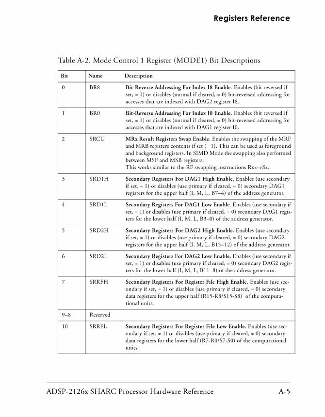
ADSP-2126x SHARC Processor Hardware Reference A-5
Registers Reference
Table A-2. Mode Control 1 Register (MODE1) Bit Descriptions
Bit Name Description
0 BR8 Bit-Reverse Addressing For Index I8 Enable. Enables (bit reversed if set, = 1) or disables (normal if cleared, = 0) bit-reversed addressing for accesses that are indexed with DAG2 register I8.
1 BR0 Bit-Reverse Addressing For Index I0 Enable. Enables (bit reversed if set, = 1) or disables (normal if cleared, = 0) bit-reversed addressing for accesses that are indexed with DAG1 register I0.
2 SRCU MRx Result Registers Swap Enable. Enables the swapping of the MRF and MRB registers contents if set (= 1). This can be used as foreground and background registers. In SIMD Mode the swapping also performed between MSF and MSB registers.This works similar to the RF swapping instructions Rx<->Sx.
3 SRD1H Secondary Registers For DAG1 High Enable. Enables (use secondary if set, = 1) or disables (use primary if cleared, = 0) secondary DAG1 registers for the upper half (I, M, L, B7–4) of the address generator.
4 SRD1L Secondary Registers For DAG1 Low Enable. Enables (use secondary if set, = 1) or disables (use primary if cleared, = 0) secondary DAG1 regis-ters for the lower half (I, M, L, B3–0) of the address generator.
5 SRD2H Secondary Registers For DAG2 High Enable. Enables (use secondary if set, = 1) or disables (use primary if cleared, = 0) secondary DAG2 registers for the upper half (I, M, L, B15–12) of the address generator.
6 SRD2L Secondary Registers For DAG2 Low Enable. Enables (use secondary if set, = 1) or disables (use primary if cleared, = 0) secondary DAG2 regis-ters for the lower half (I, M, L, B11–8) of the address generator.
7 SRRFH Secondary Registers For Register File High Enable. Enables (use sec-ondary if set, = 1) or disables (use primary if cleared, = 0) secondary data registers for the upper half (R15-R8/S15-S8) of the computa-tional units.
9–8 Reserved
10 SRRFL Secondary Registers For Register File Low Enable. Enables (use sec-ondary if set, = 1) or disables (use primary if cleared, = 0) secondary data registers for the lower half (R7-R0/S7-S0) of the computational units.

Core Registers
A-6 ADSP-2126x SHARC Processor Hardware Reference
11 NESTM Nesting Multiple Interrupts Enable. Enables (nest if set, = 1) or dis-ables (no nesting if cleared, = 0) interrupt nesting in the interrupt con-troller. When interrupt nesting is disabled, a higher priority interrupt can not interrupt a lower priority interrupt’s service routine. Other interrupts are latched as they occur, but the processor processes them after the active routine finishes. When interrupt nesting is enabled, a higher priority interrupt can interrupt a lower priority interrupt’s ser-vice routine. Lower interrupts are latched as they occur, but the proces-sor processes them after the nested routines finish.
12 IRPTEN Global Interrupt Enable. Enables (if set, = 1) or disables (if cleared, = 0) all maskable interrupts.
13 ALUSAT ALU Saturation Select. Selects whether the computational units satu-rate results on positive or negative fixed–point overflows (if 1) or return unsaturated results (if 0).
14 SSE Fixed–Point Sign Extension Select. Selects whether the computational units sign-extend short-word, 16-bit data (if 1) or zero-fill the upper 32 bits (if 0).
15 TRUNC Truncation Rounding Mode Select. Selects whether the computational units round results with round-to-zero (if 1) or round-to-nearest (if 0).
16 RND32 Rounding For 32-Bit Floating-Point Data Select. Selects whether the computational units round floating-point data to 32 bits (if 1) or round to 40 bits (if 0).
20–17 Reserved
21 PEYEN Processor Element Y Enable. Enables computations in PEy—SIMD mode—(if 1) or disables PEy—SISD mode—(if 0).When set, Processing Element Y (computation units and register files) accepts instruction dispatches. When cleared, ProcessingElement Y goes into a low power mode.Note if SIMD Mode disabled you can load data to the secondary regis-ters e.g. s0=dm(i0,m0); only computation does not work
Table A-2. Mode Control 1 Register (MODE1) Bit Descriptions (Cont’d)
Bit Name Description

ADSP-2126x SHARC Processor Hardware Reference A-7
Registers Reference
Mode Control 2 Register (MODE2)
The MODE2 register is a non memory-mapped, universal, system register (Ureg and Sreg). Figure A-2 and Table A-3 provide bit information for the MODE2 register.
22 BDCST9 Broadcast Register Loads Indexed With I9 Enable. Enables (broadcast I9 if set, = 1) or disables (no I9 broadcast if cleared, = 0) broadcast reg-ister loads for loads that use the data address generator I9 index.When the BDCST9 bit is set, data register loads from the PM data bus that use the I9 DAG2 Index register are “broadcast” to a register or reg-ister pair in each PE.
23 BDCST1 Broadcast Register Loads Indexed With I1 Enable. Enables (broadcast I1 if set, = 1) or disables (no I1 broadcast if cleared, = 0) broadcast reg-ister loads for loads that use the data address generator I1 index.When the BDCST1 bit is set, data register loads from the DM data bus that use the I1 DAG1 Index register are “broadcast” to a register or reg-ister pair in each PE.
24 CBUFEN Circular Buffer Addressing Enable. Enables (circular if set, = 1) or dis-ables (linear if cleared, = 0) circular buffer addressing for buffers with loaded I, M, B, and L DAG registers.
31–25 Reserved
Table A-2. Mode Control 1 Register (MODE1) Bit Descriptions (Cont’d)
Bit Name Description

A-8 ADSP-2126x SHARC Processor Hardware Reference
Figure A-2. MODE2 Control Register
Table A-3. Mode Control 2 Register (MODE2) Bit Descriptions
Bit Name Description
0 IRQ0E IRQ0 Sensitivity Select. Selects sensitivity for the flag configured as IRQ0 as edge-sensitive (if set, = 1) or level-sensitive (if cleared, = 0).
1 IRQ1E IRQ1 Sensitivity Select. Selects sensitivity for the flag configured as IRQ1 as edge-sensitive (if set, = 1) or level-sensitive (if cleared, = 0).
2 IRQ2E IRQ2 Sensitivity Select. Selects sensitivity for the flag configured as IRQ2 as edge-sensitive (if set, = 1) or level-sensitive (if cleared, = 0).
3 Reserved
4 CADIS Cache Disable. This bit disables the instruction cache (if set, = 1) or enables the cache (if cleared, = 0). If this bit is set, then the caching of instructions from internal memory and external memory both are disabled (see bit 6).
15 14 13 12 11 10 9 8 7 6 5 4 3 2 1 0
00 0 0 0 0 0 0 0 0 0 0 0 0 0 0
IRQ0E
CADIS
TIMEN
Timer Enable
Cache Disable
Interrupt RequestSensitivity Select
31 30 29 28 27 26 25 24 23 22 21 20 19 18 17 16
00 1 0 0 0 0 1 0 0 0 0 0 0 0 0
CAFRZ
IIRAE
U64MAE
Unaligned 64-Bit Memory Access Enable
Illegal IOP Register Access Enable
Cache Freeze
IRQ1E
Interrupt RequestSensitivity Select
IRQ2E
Interrupt Request Sensi-tivity Select
EXTCADIS
External Cache Only Disable

ADSP-2126x SHARC Processor Hardware Reference A-9
Registers Reference
Mode Mask Register (MMASK)
This is a non memory-mapped, universal, system register (Ureg and Sreg). Each bit in the MMASK register corresponds to a bit in the MODE1 register. Bits that are set in the MMASK register are used to clear bits in the MODE1 reg-ister when the processor’s status stack is pushed. This effectively disables different modes upon servicing an interrupt, or when executing a PUSH STS instruction. Figure A-3 provides bit information for the MMASK register.
5 TIMEN Timer Enable. Enables the core timer (starts, if set, = 1) or disables the core timer (stops, if cleared, = 0).
6 EXTCADIS External Cache Only Disable. Disables the caching of the instruc-tions coming from external memory (if set, =1) or enables caching of the instructions coming from external memory (if cleared, = 0 and CADIS bit 4 = 0). This bit can only be used with the ADSP-214xx products.
18–7 Reserved
19 CAFRZ Cache Freeze. Freezes the instruction cache (retain contents if set, = 1) or thaws the cache (allow new input if cleared, = 0).
20 IIRAE Illegal I/O Processor Register Access Enable. Enables (if set, = 1) or disables (if cleared, = 0) detection of I/O processor register accesses. If IIRAE is set, the processor flags an illegal access by setting the IIRA bit in the STKYx register.
21 U64MAE Unaligned 64-Bit Memory Access Enable. Enables (if set, = 1) or disables (if cleared, = 0) detection of unaligned long word accesses.If U64MAE is set, the processor flags an unaligned long word access by setting the U64MA bit in the STKYx register.
31–22 Reserved
Table A-3. Mode Control 2 Register (MODE2) Bit Descriptions (Cont’d)
Bit Name Description

A-10 ADSP-2126x SHARC Processor Hardware Reference
Arithmetic Status Registers (ASTATx and ASTATy)
The ASTATx and ASTATy registers are non memory-mapped, universal, sys-tem registers (Ureg and Sreg). Each processing element has its own ASTAT register. The ASTATx register indicates status for PEx operations, the
Figure A-3. MMASK Register Bits
31 30 29 28 27 26 25 24 23 22 21 20 19 18 17 16
00 0 0 0 0 0 0 0 0 0 1 0 0 0 0
PEYEN
BDCST9
RND32
BDCST1
CBUFEN
Circular Buffer Addressing Enable
Broadcast Register Loads
Broadcast Register Loads
Processor Element Y Enable
Rounding For 32-BitFloating-Point Data Select
15 14 13 12 11 10 9 8 7 6 5 4 3 2 1 0
00 0 0 0 0 0 0 0 0 0 0 0 0 0 0
BR0
SRCU
IRPTEN
BR8
ALUSAT
SSE
TRUNC
Truncation Rounding Mode Select
Fixed-Point Sign Extension Select
ALU Saturation Select
Global Interrupt Enable
Secondary Registers Computational Units Enable
Bit Reverse Addressing for I0
Bit-Reverse Addressing for I8
NESTM
Nesting Multiple Interrupts Enable
SRD1H
SRD1L
Secondary Registers DAG1 Low Enable
Secondary Registers DAG1 High Enable
SRRFL
Secondary Registers Register File Low Enable
SRD2H
Secondary Registers DAG2 High Enable
SRD2L
Secondary Registers DAG2 Low Enable
SRRFH
Secondary Registers Register File High Enable

ADSP-2126x SHARC Processor Hardware Reference A-11
Registers Reference
ASTATy register indicates status for PEy operations. Figure A-4 and Table A-4 provide bit information for the ASTAT registers.
If these registers are loaded manually, there is a one cycle effect latency before the new value in the ASTATx register can be used in a
Figure A-4. ASTAT Register
15 14 13 12 11 10 9 8 7 6 5 4 3 2 1 0
00 0 0 0 0 0 0 0 0 0 0 0 0 0 0
AF
SV
SZ
SSShifter Input Sign
Shifter Zero
Shifter Overflow
ALU Floating-Point Operation
MIMultiplier Floating-Point Invalid Operation
MUMultiplier Floating-Point Underflow
MVMultiplier Overflow
AC
AN
AV
AZALU Zero/Float-ing-Point Underflow
ALU Overflow
ALU Negative
ALU Fixed-Point Carry
ASALU X-Input Sign (for ABS and MANT)
AIALU Floating-Point Invalid Operation
MNMultiplier Negative
31 30 29 28 27 26 25 24 23 22 21 20 19 18 17 16
00 0 0 0 0 0 0 0 0 0 0 0 0 0 0
BTFCACC (31–24)
Compare Accumulation Shift BitsBit Test Flag for System Registers
SFShifter Bit FIFO

Core Registers
A-12 ADSP-2126x SHARC Processor Hardware Reference
conditional instruction.
Table A-4. ASTATx and ASTATy Register Bit Descriptions
Bit Name Description
0 AZ ALU Zero/Floating-Point Underflow. Indicates if the last ALU operation’s result was zero (if set, = 1) or non-zero (if cleared, = 0). The ALU updates AZ for all fixed-point and floating-point ALU operations. AZ can also indicate a floating-point underflow. During an ALU underflow (indicated by a set (= 1) AUS bit in the STKYx/y register), the processor sets AZ if the floating-point result is smaller than can be represented in the output for-mat.
1 AV ALU Overflow. Indicates if the last ALU operation’s result overflowed (if set, = 1) or did not overflow (if cleared, = 0). The ALU updates AV for all fixed-point and floating-point ALU operations. For fixed-point results, the processor sets AV and the AOS bit in the STKYx/y register when the XOR of the two most significant bits (MSBs) is a 1. For floating-point results, the processor sets AV and the AVS bit in the STKYx/y register when the rounded result overflows (unbiased exponent > 127).
2 AN ALU Negative. Indicates if the last ALU operation’s result was negative (if set, = 1) or positive (if cleared, = 0). The ALU updates AN for all fixed-point and floating-point ALU operations.
3 AC ALU Fixed-Point Carry. Indicates if the last ALU operation had a carry out of the MSB of the result (if set, = 1) or had no carry (if cleared, = 0). The ALU updates AC for all fixed-point operations. The processor clears AC during the fixed-point logic operations: PASS, MIN, MAX, COMP, ABS, and CLIP. The ALU reads the AC flag for the fixed-point accumulate oper-ations: Addition with Carry and Fixed-point Subtraction with Carry.
4 AS ALU X-Input Sign (for ABS and MANT). Indicates if the last ALU ABS or MANT operation’s input was negative (if set, = 1) or positive (if cleared, = 0). The ALU updates AS only for fixed- and floating-point ABS and MANT operations. The ALU clears AS for all operations other than ABS and MANT.

ADSP-2126x SHARC Processor Hardware Reference A-13
Registers Reference
5 AI ALU Floating-Point Invalid Operation. Indicates if the last ALU opera-tion’s input was invalid (if set, = 1) or valid (if cleared, = 0). The ALU updates AI for all fixed- and floating-point ALU operations. The processor sets AI and AIS in the STKYx/y register if the ALU operation:• Receives a NAN input operand• Adds opposite-signed infinities• Subtracts like-signed infinities• Overflows during a floating-point to fixed-point conversion when satu-
ration mode is not set• Operates on an infinity when the saturation mode is not set
6 MN Multiplier Negative. Indicates if the last multiplier operation’s result was negative (if set, = 1) or positive (if cleared, = 0). The multiplier updates MN for all fixed- and floating-point multiplier operations.
7 MV Multiplier Overflow. Indicates if the last multiplier operation’s result over-flowed (if set, = 1) or did not overflow (if cleared, = 0). The multiplier updates MV for all fixed-point and floating-point multiplier operations. For floating-point results, the processor sets MV and MVS in the STKYx/y register if the rounded result overflows (unbiased exponent > 127). For fixed-point results, the processor sets MV and the MOS bit in the STKYx/y register if the result of the multiplier operation is:• Twos-complement, fractional with the upper 17 bits of MR not all zeros
or all ones• Twos-complement, integer with the upper 49 bits of MR not all zeros or
all ones• Unsigned, fractional with the upper 16 bits of MR not all zeros• Unsigned, integer with the upper 48 bits of MR not all zerosIf the multiplier operation directs a fixed-point result to an MR register, the processor places the overflowed portion of the result in MR1 and MR2 for an integer result or places it in MR2 only for a fractional result.
Table A-4. ASTATx and ASTATy Register Bit Descriptions (Cont’d)
Bit Name Description

Core Registers
A-14 ADSP-2126x SHARC Processor Hardware Reference
8 MU Multiplier Floating-Point Underflow. Indicates if the last multiplier opera-tion’s result underflowed (if set, = 1) or did not underflow(if cleared, = 0). The multiplier updates MU for all fixed- and float-ing-point multiplier operations. For floating-point results, the processor sets MU and the MUS bit in the STKYx/y register if the floating-point result underflows (unbiased exponent < –126). Denormal operands are treated as zeros, therefore they never cause underflows. For fixed-point results, the processor sets MU and the MUS bit in the STKYx/y register if the result of the multiplier operation is:• Twos-complement, fractional: with upper 48 bits all zeros or all ones,
lower 32 bits not all zeros• Unsigned, fractional: with upper 48 bits all zeros, lower 32 bits not all
zerosIf the multiplier operation directs a fixed-point, fractional result to an MR register, the processor places the underflowed portion of the result in MR0.
9 MI Multiplier Floating-Point Invalid Operation. Indicates if the last multi-plier operation’s input was invalid (if set, = 1) or valid (if cleared, = 0).The multiplier updates MI for floating-point multiplier operations. The processor sets MI and the MIS bit in the STKYx/y register if the ALU oper-ation:• Receives a NAN input operand• Receives an Infinity and zero as input operands
10 AF ALU Floating-Point Operation. Indicates if the last ALU operation was floating-point (if set, = 1) or fixed-point (if cleared, = 0). The ALU updates AF for all fixed-point and floating-point ALU operations.
11 SV Shifter Overflow. Indicates if the last shifter operation’s result overflowed (if set, = 1) or did not overflow (if cleared, = 0). The shifter updates SV for all shifter operations. The processor sets SV if the shifter operation:• Shifts the significant bits to the left of the 32-bit fixed-point field• Tests, sets, or clears a bit outside of the 32-bit fixed-point field• Extracts a field that is past or crosses the left edge of the 32-bit
fixed-point field• Performs a LEFTZ or LEFTO operation that returns a result of 32
12 SZ Shifter Zero. Indicates if the last shifter operation’s result was zero (if set, = 1) or non-zero (if cleared, = 0). The shifter updates SZ for all shifter operations. The processor also sets SZ if the shifter operation per-forms a bit test on a bit outside of the 32-bit fixed-point field.
Table A-4. ASTATx and ASTATy Register Bit Descriptions (Cont’d)
Bit Name Description
ADSP-2126x SHARC Processor Hardware Reference A-15
Registers Reference
Sticky Status Registers (STKYx and STKYy)
These are non memory-mapped, universal, system registers (Ureg and Sreg). Each processing element has its own STKY register. The STKYx regis-ter indicates status for PEx operations and some program sequencer stacks. The STKYy register only indicates status for PEy operations.
STKY bits do not clear themselves after the condition they flag is no longer true. They remain “sticky” until cleared by the program.
The processor sets a STKY bit in response to a condition. For example, the processor sets the AUS bit in the STKY register when an ALU underflow set AZ in the ASTAT register. The processor clears AZ if the next ALU operation does not cause an underflow. The AUS bit remains set until a program
13 SS Shifter Input Sign. Indicates if the last shifter operation’s input was nega-tive (if set, = 1) or positive (if cleared, = 0). The shifter updates SS for all shifter operations.
14 SF ShifterBit FIFO. Indicates the current value of Write Pointer. SF is set when write pointer is greater than or equal to 32, otherwise it is cleared.(upon ADSP-2146x processors only)
17–15 Reserved
18 BTF Bit Test Flag for System Registers. Indicates if the system register bit is true (if set, = 1) or false (if cleared, = 0). The processor sets BTF when the bit(s) in a system register and value in the Bit Tst instruction match. The processor also sets BTF when the bit(s) in a system register and value in the Bit Xor instruction match.
23–19 Reserved
31–24 CACC Compare Accumulation Shift Register. Bit 31 of CACC indicates which operand was greater during the last ALU compare operation: X input (if set, = 1) or Y input (if cleared, = 0). The other seven bits in CACC form a right-shift register, each storing a previous compare accumulation result. With each new compare, the processor right shifts the values of CACC, storing the newest value in bit 31 and the oldest value in bit 24.
Table A-4. ASTATx and ASTATy Register Bit Descriptions (Cont’d)
Bit Name Description
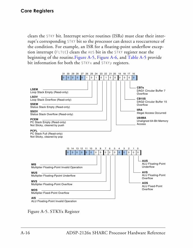
Core Registers
A-16 ADSP-2126x SHARC Processor Hardware Reference
clears the STKY bit. Interrupt service routines (ISRs) must clear their inter-rupt’s corresponding STKY bit so the processor can detect a reoccurrence of the condition. For example, an ISR for a floating-point underflow excep-tion interrupt (FLTUI) clears the AUS bit in the STKY register near the beginning of the routine.Figure A-5, Figure A-6, and Table A-5 provide bit information for both the STKYx and STKYy registers.
Figure A-5. STKYx Register
15 14 13 12 11 10 9 8 7 6 5 4 3 2 1 0
00 0 0 0 0 0 0 0 0 0 0 0 0 0 0
PCEM
SSOV
LSOVLoop Stack Overflow (Read-only)
Status Stack Overflow (Read-only)
PC Stack Empty (Read-only)Not Sticky, cleared by push
Multiplier Floating-Point Invalid OperationMIS
Multiplier Floating-Ppoint UnderflowMUS
U64MA
IIRA
CB15S
CB7sDAG1 Circular Buffer 7 Overflow
DAG2 Circular Buffer 15 Overflow
Illegal Access Occurred
Unaligned 64-Bit Memory Access
AOS
ALU Floating-Point Overflow
AUS
AVS
ALU Floating-Point Underflow
31 30 29 28 27 26 25 24 23 22 21 20 19 18 17 16
00 0 0 0 0 1 0 1 0 1 0 0 0 0 0
LSEMLoop Stack Empty (Read-only)
PCFLPC Stack Full (Read-only)Not Sticky, cleared by pop
SSEMStatus Stack Empty (Read-only)
ALU Fixed-Point Overflow
AISALU Floating-Point Invalid Operation
Multiplier Floating-Point OverflowMVS
Multiplier Fixed-Point OverflowMOS

ADSP-2126x SHARC Processor Hardware Reference A-17
Registers Reference
Figure A-6. STKYy Register
Table A-5. STKYx and STKYy Register Bit Descriptions
Bit Name Description: √ shows bits in both STKYx/y × shows bits in STKYx only
0 AUS ALU Floating-Point Underflow. A sticky indicator for the ALU AS bit. For more information, see “AZ” on page A-12.
√
1 AVS ALU Floating-Point Overflow. A sticky indicator for the ALU AV bit. For more information, see “AV” on page A-12.
√
2 AOS ALU Fixed-Point Overflow. A sticky indicator for the ALU AV bit. For more information, see “AV” on page A-12.
√
4–3 Reserved
5 AIS ALU Floating-Point Invalid Operation. A sticky indicator for the ALU AI bit. For more information, see “AI” on page A-13.
√
6 MOS Multiplier Fixed-Point Overflow. A sticky indicator for the mul-tiplier MV bit. For more information, see “MV” on page A-13.
√
15 14 13 12 11 10 9 8 7 6 5 4 3 2 1 0
00 0 0 0 0 0 0 0 0 0 0 0 0 0 0
Multiplier Floating-Point Invalid Operation
MIS
Multiplier Floating-Point UnderflowMUS
AOS
ALU Floating-Point Overflow
AUS
AVS
ALU Fixed-Point Overflow
AISALU Floating-Point Invalid Operation
Multiplier Floating-Point OverflowMVS
Multiplier Fixed-Point OverflowMOS
ALU Floating-Point Underflow
31 30 29 28 27 26 25 24 23 22 21 20 19 18 17 16
00 0 0 0 0 1 0 1 0 1 0 0 0 0 0

Core Registers
A-18 ADSP-2126x SHARC Processor Hardware Reference
7 MVS Multiplier Floating-Point Overflow. A sticky indicator for the multiplier MV bit. For more information, see “MV” on page A-13.
√
8 MUS Multiplier Floating-Point Underflow. A sticky indicator for the multiplier MU bit. For more information, see “MU” on page A-14.
√
9 MIS Multiplier Floating-Point Invalid Operation. A sticky indicator for the multiplier MI bit. For more information, see “MI” on page A-14.
√
16–10 Reserved
17 CB7S DAG1 Circular Buffer 7 Overflow. Indicates if a circular buffer being addressed with DAG1 register I7 has overflowed (if set, = 1) or has not overflowed (if cleared, = 0). A circular buffer overflow occurs when DAG circular buffering operation increments the I register past the end of buffer.
×
18 CB15S DAG2 Circular Buffer 15 Overflow. Indicates if a circular buffer being addressed with DAG2 register I15 has overflowed (if set, = 1) or has not overflowed (if cleared, = 0). A circular buffer over-flow occurs when DAG circular buffering operation increments the I register past the end of buffer.
×
19 IIRA Illegal IOP Register Access. Indicates if set (= 1) the core had accessed the IOP register space or not.
×
20 U64MA Unaligned 64-Bit Memory Access. Indicates if set (= 1) if a Nor-mal word access with the LW mnemonic addressing an uneven memory address has occurred or has not occurred (if 0).
×
21 PCFL PC Stack Full. Indicates if the PC stack is full (if 1) or not full (if 0)—Not a sticky bit, cleared by a Pop.
×
22 PCEM PC Stack Empty. Indicates if the PC stack is empty (if 1) or not empty (if 0)—Not sticky, cleared by a Push.
×
23 SSOV Status Stack Overflow. Indicates if the status stack is overflowed (if 1) or not overflowed (if 0)—sticky bit.
×
Table A-5. STKYx and STKYy Register Bit Descriptions (Cont’d)
Bit Name Description: √ shows bits in both STKYx/y × shows bits in STKYx only

ADSP-2126x SHARC Processor Hardware Reference A-19
Registers Reference
User-Defined Status Registers (USTATx)
These are non-memory-mapped, universal, system registers (Ureg and Sreg). The reset value for these registers is 0x0000 0000. The USTATx reg-isters are user-defined, general-purpose status registers. Programs can use these 32-bit registers with bit-wise instructions (SET, CLEAR, TEST, and oth-ers). Often, programs use these registers for low overhead, general-purpose flags or for temporary 32-bit storage of data.
Processing Element RegistersExcept for the PX register, the DSP’s Processing Element registers store data for each element’s ALU, multiplier, and shifter. The inputs and out-puts for processing element operations go through these registers. The PX
24 SSEM Status Stack Empty. Indicates if the status stack is empty (if 1) or not empty (if 0)—not sticky, cleared by a Push.
×
25 LSOV Loop Stack Overflow. Indicates if the loop counter stack and loop stack are overflowed (if 1) or not overflowed (if 0)—sticky bit.
×
26 LSEM Loop Stack Empty. Indicates if the loop counter stack and loop stack are empty (if 1) or not empty (if 0)—not sticky, cleared by a Push.
×
31–27 Reserved
Table A-5. STKYx and STKYy Register Bit Descriptions (Cont’d)
Bit Name Description: √ shows bits in both STKYx/y × shows bits in STKYx only

Core Registers
A-20 ADSP-2126x SHARC Processor Hardware Reference
register lets programs transfer data between the data buses, but cannot be an input or output in a calculation.
Data File Data Registers (Rx, Sx)
The Data File Data registers are non memory-mapped, universal, data reg-isters (Ureg and Dreg). Each of the DSP’s processing elements has a data register file—a set of 40-bit data registers that transfer data between the data buses and the computation units. These registers also provide local storage for operands and results.
The R and S prefixes on register names do not effect the 32-bit or 40-bit data transfer; the naming convention determines how the ALU, multi-plier, and shifter treat the data and determines which processing element’s data registers are being used. For more information on how to use these registers, see “Data Register File” on page 2-37.
Alternate Data File Data Registers (Rx’, Sx’)
The processor includes alternate register sets for all data registers to facili-tate fast context switching. Bits in the MODE1 register control when alternate registers become accessible. While inaccessible, the contents of alternate registers are not affected by processor operations. Note that there is an one cycle latency between writing to MODE1 and being able to access an alternate register set.
Table A-6. Processing Element Registers
Register Name and Page Reference Initialization After Reset
“Data File Data Registers (Rx, Sx)” on page A-20 Undefined
“PEx Multiplier Result Registers (MRFx, MRBx)” on page A-21 Undefined
“Program Memory Bus Exchange Register (PX)” on page A-22 Undefined

ADSP-2126x SHARC Processor Hardware Reference A-21
Registers Reference
PEx Multiplier Result Registers (MRFx, MRBx)
The MRFx and MRBx registers are non memory-mapped. The PEx unit has a primary or foreground (MRF) register and alternate or background (MRB) results register. Fixed-point operations place 80-bit results in the multi-plier’s foreground MRF register or background MRB register, depending on which is active. For more information on selecting the Result register, see “Alternate (Secondary) Data Registers” on page 2-39. For more informa-tion on result register fields, see “Data Register File” on page 2-37.
Figure A-7. MRFx and MRBx Registers
MV SET
Integer Multiplier Fixed-point Result Placement
0316379
INTEGER RESULTINTEGER RESULTOVERFLOW
MR2 MR1 MR0
UREG ZEROS
8 BITS32 BITS
REGISTER FILEPLACEMENT
MRF OR MRBPLACEMENT
BINARY POINT
INTEGER RESULTOVERFLOW (IS LOST)
UREG ZEROS
T
32 BITS
0316379
FRACTIONAL RESULTOVERFLOW
MR2 MR1 MR0
Fractional Multiplier Fixed-point Result Placement
MRF OR MRBPLACEMENT
REGISTER FILEPLACEMENT
FRACTIONAL RESULT UNDERFLOW (IS LOST)
BINARY POINT
FRACTIONAL RESULT
MV SET8 BITS

Core Registers
A-22 ADSP-2126x SHARC Processor Hardware Reference
PEy Multiplier Result Registers (MSFx, MSBx)
The MSFx and MSBx registers are non memory-mapped. The PEy unit has a primary or foreground (MSF) register and alternate or background (MSB) results register. Fixed-point operations place 80-bit results in the multiplier’s foreground MSF register or background MSB register, depending on which is active. For more information on selecting the Result register, see “Alternate (Secondary) Data Registers” on page 2-39. For more information on result register fields, see “Data Register File” on page 2-37.
Program Memory Bus Exchange Register (PX)
The PX register is a non-memory-mapped, universal registers (Ureg only). The PM Bus Exchange (PX) register permits data to flow between the PM and DM data buses. The PX register can work as one 64-bit register or as two 32-bit registers (PX1 and PX2). The PX1 register is the lower 32 bits of the PX register and PX2 is the upper 32 bits of PX. See the section “Internal Data Bus Exchange” on page 5-6 for more information about the PX register.
Program Sequencer RegistersThe DSP’s program sequencer registers direct the execution of instruc-tions. These registers include support for the:
• Instruction pipeline
• Program and loop stacks
• Timer
• Interrupt mask and latch

ADSP-2126x SHARC Processor Hardware Reference A-23
Registers Reference
Interrupt Latch Register (IRPTL)
The IRPTL register is a non-memory-mapped, universal, system register (Ureg and Sreg). The IRPTL register indicates latch status for interrupts. Figure A-8 and Table A-9 provide bit definitions for the IRPTL register.
The programmable interrupt latch bits (P0I–P5I, P14I–P16I) are con-trolled through the priority interrupt control registers (PICR). The descriptions provided are their default source. For information on their
Table A-7. Program Sequencer Registers
Register Initialization After Reset
“Interrupt Latch Register (IRPTL)” on page A-23 0x0000 0000 (cleared)
“Interrupt Mask Register (IMASK)” on page A-24 0x0000 0003
“Interrupt Mask Pointer Register (IMASKP)” on page A-24 0x0000 0000 (cleared)
“Interrupt Register (LIRPTL)” on page A-29 0x0000 0000 (cleared)
Table A-8. Program Counter Registers
Register Initialization After Reset
“Program Counter Register (PC)” on page A-32 Undefined
“Program Counter Stack Register (PCSTK)” on page A-33 Undefined
“Program Counter Stack Pointer Register (PCSTKP)” on page A-33
Undefined
“Fetch Address Register (FADDR)” on page A-34 Undefined
“Decode Address Register (DADDR)” on page A-34 Undefined
“Loop Address Stack Register (LADDR)” on page A-34 Undefined
“Current Loop Counter Register (CURLCNTR)” on page A-35 Undefined
“Loop Counter Register (LCNTR)” on page A-35 Undefined
“Timer Period Register (TPERIOD)” on page A-35 Undefined
“Timer Count Register (TCOUNT)” on page A-36 Undefined
Core Registers
A-24 ADSP-2126x SHARC Processor Hardware Reference
optional use, see “Programmable Interrupt Control Registers (PICRx)” in the processor specific hardware reference.
Interrupt Mask Register (IMASK)
The IMASK register is a non-memory-mapped, universal, system register (Ureg and Sreg). Each bit in the IMASK register corresponds to a bit with the same name in the IRPTL registers. The bits in the IMASK register unmask (enable if set, = 1), or mask (disable if cleared, = 0) the interrupts that are latched in the IRPTL register. Except for the RSTI and EMUI bits, all interrupts are maskable.
When the IMASK register masks an interrupt, the masking disables the pro-cessor’s response to the interrupt. The IRPTL register still latches an interrupt even when masked, and the processor responds to that latched interrupt if it is later unmasked. Figure A-8 and Table A-9 provide bit definitions for the IMASK register.
Interrupt Mask Pointer Register (IMASKP)
The IMASKP register is a non-memory-mapped, universal, system register (Ureg and Sreg). Each bit in the IMASKP register corresponds to a bit with the same name in the IRPTL registers. The IMASKP register field descrip-tions are shown in Figure A-8, and described in Table A-9. Shaded cells indicate user programmable interrupts.
This register supports an interrupt nesting scheme that lets higher priority events interrupt an ISR and keeps lower priority events from interrupting.
When interrupt nesting is enabled, the bits in the IMASKP register mask interrupts that have a lower priority than the interrupt that is currently being serviced. Other bits in this register unmask interrupts having higher priority than the interrupt that is currently being serviced. Interrupt nest-ing is enabled using NESTM in the MODE1 register. The IRPTL register latches a lower priority interrupt even when masked, and the processor responds to that latched interrupt if it is later unmasked.

ADSP-2126x SHARC Processor Hardware Reference A-25
Registers Reference
When interrupt nesting is disabled (NESTM = 0 in the MODE1 register), the bits in the IMASKP register mask all interrupts while an interrupt is cur-rently being serviced. The IRPTL register still latches these interrupts even when masked, and the processor responds to the highest priority latched interrupt after servicing the current interrupt.

Core Registers
A-26 ADSP-2126x SHARC Processor Hardware Reference
Figure A-8. IRPTL, IMASK, and IMASKP Registers
31 30 29 28 27 26 25 24 23 22 21 20 19 18 17 16
00 0 0 0 0 0 0 0 0 0 0 0 0 0 0
TMZLI
P5ISFT3IUser Software Interrupt 3
Timer Expired Low Priority
CB15I
Programmable Interrupt 5 SFT2IUser Software Interrupt 2 SFT1IUser Software Interrupt 1
SFT0IUser Software Interrupt 0
EMULIEmulator Interrupt
FLTIIFloating-point Invalid Operation
Floating-point UnderflowFLTUI
CB7I
DAG1 Circular Buffer 15Overflow
FIXIFixed-point Overflow
FLTOIFloating-point Overflow
DAG1 Circular Buffer 7IOverflow
P15IProgrammable Interrupt 15
P14I
P16I
Programmable Interrupt 14 (DPI)
Programmable Interrupt 16
15 14 13 12 11 10 9 8 7 6 5 4 3 2 1 0
00 0 0 0 0 0 0 0 0 0 0 0 0 0 0
SOVFI
EMUIP4IProgrammable Interrupt 4
Stack Full/Overflow
Reset
IICDI
Emulator Interrupt P3IProgrammable Interrupt 3 P2IProgrammable Interrupt 2
P1IProgrammable Interrupt 1
P0IProgrammable Interrupt 0
IRQ0IIRQ0_I Hardware Interrupt
IRQ1_I Hardware Interrupt IRQ1I
RSTI
Illegal Input Condition Detected
TMZHITimer Expired High Priority
Hardware Breakpoint Interrupt
IRQ2_I Hardware Interrupt IRQ2I
BKPI
SPERRISPORT Error Interrupt

ADSP-2126x SHARC Processor Hardware Reference A-27
Registers Reference
Table A-9. IRPTL, IMASK, IMASKP Register Bit Descriptions
Bit Name Definition
0 EMUI Emulator Interrupt. An EMUI occurs when the external emulator trig-gers an interrupt or the core hits a emulator breakpoint.Note this interrupt has highest priority, it is read-only and non-mask-able
1 RSTI Reset Interrupt. An RSTI occurs as an external device asserts the RESET pin or after a software reset (SYSCTL register). Note this inter-rupt is read-only and non-maskable.
2 IICDI Illegal Input Condition Detected Interrupt. An IICDI occurs when a TRUE results from the logical OR’ing of the illegal I/O processor regis-ter access (IIRA) and unaligned 64-bit memory access bits in the STKYx registers.
3 SOVFI Stack Overflow/Full Interrupt. A SOVFI occurs when a stack in the program sequencer overflows or is full.
4 TMZHI Core Timer Expired High Priority. A TMZHI occurs when the timer decrements to zero. Note that this event also triggers a TMZLI. Since the timer expired event (TCOUNT decrements to zero) generates two interrupts, TMZHI and TMZLI, programs should unmask the timer interrupt with the desired priority and leave the other one masked.
5 SPERRI1 Sport Error Interrupt. A SPERRI occurs on a FIFO underflow/over-flow or a frame sync error.
6 BKPI Hardware Breakpoint Interrupt. When the processor is servicing another interrupt, indicates if the BKPI interrupt is unmasked (if set, = 1), or masked (if cleared, = 0).
7 Reserved
8 IRQ2I Hardware Interrupt. An IRQ2I occurs when an external device asserts the FLAG2 pin configured as IRQ2. The IRQ2E bit (MODE2) defines if interrupt latched on edge or level.
9 IRQ1I Hardware Interrupt. An IRQ1I occurs when an external device asserts the FLAG2 pin configured as IRQ1. The IRQ1E bit (MODE2) defines if interrupt latched on edge or level.
10 IRQ0I Hardware Interrupt. An IRQ0I occurs when an external device asserts the FLAG2 pin configured as IRQ0. The IRQ0E bit (MODE2) defines if interrupt latched on edge or level.

Core Registers
A-28 ADSP-2126x SHARC Processor Hardware Reference
11 P0I Programmable Interrupt 0. A P0I interrupt occurs when the default/programmed peripheral sets (= 1) this bit.
12 P1I Programmable Interrupt 1. See P0I
13 P2I Programmable Interrupt 2. See P0I
14 P3I Programmable Interrupt 3. See P0I
15 P4I Programmable Interrupt 4. See P0I
16 P5I Programmable Interrupt 5. See P0I
17 P14I Programmable Interrupt 14. See P0I
18 P15I Programmable Interrupt 15. See P0I
19 P16I Programmable Interrupt 16. See P0I
20 CB7I DAG1 Circular Buffer 7 Overflow Interrupt. A circular buffer over-flow occurs when the DAG circular buffering operation increments the I7 register past the end of the buffer.
21 CB15I DAG2 Circular Buffer 15 Overflow Interrupt. A circular buffer over-flow occurs when the DAG circular buffering operation increments the I15 register past the end of the buffer.
22 TMZLI Core Timer Expired (Low Priority) Interrupt. A TMZLI occurs when the timer decrements to zero. (Refer to TMZHI)
23 FIXI Fixed-Point Overflow Interrupt. Refer to the status registers for the execution units (ASTATx/y, STKYx/y).
24 FLTOI Floating-Point Overflow Interrupt. Refer to the status registers for the execution units (ASTATx/y, STKYx/y).
25 FLTUI Floating-Point Underflow Interrupt. Refer to the status registers for the execution units (ASTATx/y, STKYx/y).
26 FLTII Floating-Point Invalid Operation Interrupt. Refer to the status regis-ters for the execution units (ASTATx/y, STKYx/y).
27 EMULI Emulator Low Priority Interrupt. An EMULI occurs during Back-ground telemetry channels (BTC). This interrupt has a lower priority than EMUI, but higher priority than software interrupts.
Table A-9. IRPTL, IMASK, IMASKP Register Bit Descriptions (Cont’d)
Bit Name Definition

ADSP-2126x SHARC Processor Hardware Reference A-29
Registers Reference
Interrupt Register (LIRPTL)
The LIRPTL register is a non-memory-mapped, universal, system register (Ureg and Sreg). The LIRPTL register indicates latch status, select masking, and displays mask pointers for interrupts. Figure A-9 and Table A-10 pro-vide bit definitions for the LIRPTL register.
The MSKP bits in the LIRPTL register, and the entire IMASKP register are for interrupt controller use only. Modifying these bits interferes with the proper operation of the interrupt controller.
The programmable interrupt latch bits (P6I–P13I, P17I, P18I) are con-trolled through the programmable interrupt controller registers (PICRx). The descriptions provided are their default source. For information on their optional use, see “Programmable Interrupt Priority Control Regis-ters” in the product related hardware reference.
28 SFT0I User Software Interrupt 0. An SFT0I occurs when a program sets (= 1) this bit.
29 SFT1I User Software Interrupt 1. See SFT01.
30 SFT2I User Software Interrupt 2. See SFT01.
31 SFT3I User Software Interrupt 3. See SFT01. Lowest priority.
1 The SPERRI interrupt (bit 5) is reserved for ADSP-21362/3/4/5/6 SHARC processors.
Table A-9. IRPTL, IMASK, IMASKP Register Bit Descriptions (Cont’d)
Bit Name Definition

Core Registers
A-30 ADSP-2126x SHARC Processor Hardware Reference
Figure A-9. LIRPTL Register
15 14 13 12 11 10 9 8 7 6 5 4 3 2 1 0
00 0 0 0 0 0 0 0 0 0 0 0 0 0 0
P13I
P9IMSK
P10IProgrammable Interrupt 10
Programmable Interrupt 12 P12I
P10IMASKProgrammable Interrupt 10
P8IMSKProgrammable Interrupt 8 Mask
Programmable Interrupt 9 Mask
P7IMSKProgrammable Interrupt 7 Mask P6IMSKProgrammable Interrupt 6 Mask P18IProgrammable Interrupt 18
P6IProgrammable Interrupt 6
P7IProgrammable Interrupt 7 P8IProgrammable Interrupt 8 P9IProgrammable Interrupt 9
P17IProgrammable Interrupt 17
Programmable Interrupt 13
31 30 29 28 27 26 25 24 23 22 21 20 19 18 17 16
00 0 0 0 0 0 0 0 0 0 0 0 0 0 0
P13IMSK
P12IMSKProgrammable Interrupt 12 Mask P18IMSKP
Programmable Interrupt 18 Mask Pointer P17IMSKPProgrammable Interrupt 17 Mask Pointer P13MASKP
Programmable Interrupt 12 Mask P12IMSKP
Programmable Interrupt 9 Mask
P10IMSKPProgrammable Interrupt 10 Mask P9IMSKP
P17IMSKProgrammable Interrupt 17 Mask P18IMSKProgrammable Interrupt 18 Mask P6IMSKPProgrammable Interrupt 6 Mask Pointer P7IMSKPProgrammable Interrupt 7 Mask Pointer
P8IMSKPProgrammable Interrupt 8 Mask Pointer
Programmable Interrupt 13 Mask
Programmable Interrupt 13 Mask
Programmable Interrupt 11 P11I
P11IMASKProgrammable Interrupt 11
P11IMSKPProgrammable Interrupt 11 Mask

ADSP-2126x SHARC Processor Hardware Reference A-31
Registers Reference
Table A-10. LIRPTL Register Bit Descriptions
Bit Name Definition
0 P6I Programmable Interrupt 6.
1 P7I Programmable Interrupt 7
2 P8I Programmable Interrupt 8
3 P9I Programmable Interrupt 9
4 P10I Programmable Interrupt 10
5 P11I Programmable Interrupt 11
6 P12I Programmable Interrupt 12
7 P13I Programmable Interrupt 13
8 P17I Programmable Interrupt 17
9 P18I Programmable Interrupt 18
10 P6IMSK Programmable Interrupt Mask 6. Unmasks the P6I interrupt (if set, = 1),or masks the P6I interrupt (if cleared, = 0).
11 P7IMSK Programmable Interrupt Mask 7. See P6IMSK.
12 P8IMSK Programmable Interrupt Mask 8. See P6IMSK.
13 P9IMSK Programmable Interrupt Mask 9. See P6IMSK.
14 P10IMSK Programmable Interrupt Mask 9. See P6IMSK.
15 P11IMSK Programmable Interrupt Mask 11. See P6IMSK.
16 P12IMSK Programmable Interrupt Mask 12. See P6IMSK.
17 P13IMSK Programmable Interrupt Mask 12. See P6IMSK.
18 P17IMSK Programmable Interrupt Mask 17. See P6IMSK.
19 P18IMSK Programmable Interrupt Mask 18. See P6IMSK.
20 P6IMSKP Programmable Interrupt Mask Pointer 9. When the proces-sor is servicing another interrupt, indicates if the P6I inter-rupt is unmasked (if set, = 1), or the P6I interrupt is masked (if cleared, = 0).

Core Registers
A-32 ADSP-2126x SHARC Processor Hardware Reference
Program Counter Register (PC)
The PC register is a non-memory-mapped, universal register (Ureg only). The Program Counter register is the last stage in the fetch-decode-execute instruction pipeline and contains the 24-bit address of the instruction that the DSP executes on the next cycle. The PC couples with the Program Counter Stack, PCSTK, which stores return addresses and top-of-loop addresses. All addresses generated by the sequencer are 24-bit program memory instruction addresses.
As shown in Figure A-10, the address buses can handle 32-bit addresses, but the program sequencer only generates 24-bit addresses over the PM bus.
21 P7IMSKP Programmable Interrupt Mask Pointer 7. See P6IMSKP.
22 P8IMSKP Programmable Interrupt Mask Pointer 8. See P6IMSKP.
23 P9IMSKP Programmable Interrupt Mask Pointer 9. See P6IMSKP.
24 P10IMSKP Programmable Interrupt Mask Pointer 10. See P6IMSKP.
25 P11IMSKP Programmable Interrupt Mask Pointer 11. See P6IMSKP.
26 P12IMSKP Programmable Interrupt Mask Pointer 12. See P6IMSKP.
27 P13IMSKP Programmable Interrupt Mask Pointer 13. See P6IMSKP.
28 P17IMSKP Programmable Interrupt Mask Pointer 17. See P6IMSKP.
29 P18MSKP Programmable Interrupt Mask Pointer 18. See P6IMSKP.
31–30 Reserved
Table A-10. LIRPTL Register Bit Descriptions (Cont’d)
Bit Name Definition

ADSP-2126x SHARC Processor Hardware Reference A-33
Registers Reference
Program Counter Stack Register (PCSTK)
This is a non-memory-mapped, universal register (Ureg only). The Pro-gram Counter Stack register contains the address of the top of the PC stack. This register is a readable and writable register.
Program Counter Stack Pointer Register (PCSTKP)
The PCSTKP register is a non-memory-mapped, universal register (Ureg only). The Program Counter Stack Pointer register contains the value of PCSTKP. This value is given as follows: 0 when the PC stack is empty, 1...30 when the stack contains data, and 31 when the stack overflows. This regis-ter is readable and writable. A write to PCSTKP takes effect after a one-cycle delay. If the PC stack is overflowed, a write to PCSTKP has no effect.
Figure A-10. PM and DM Bus Addresses Versus Sequencing Addresses
PM and DM Address Buses and DAGs Can Handle 32-Bit Addresses
Program Sequencer Handles
S Field
Bits 20-18, System (Internal) Memory
Bits 31-21, All zeros
31 23 21 20 18 17 0
System Values in this field have the following meaning:
000- Address of an IOP register001- Address in Long Word space01x- Address in Normal Word space1xx- Address in Short Word space
24-Bit Addresses
17-16 = 00; IOP peripheral17-16 = 11; IOP core

Core Registers
A-34 ADSP-2126x SHARC Processor Hardware Reference
Status Stack Register (STS)
The STS register is a status stack register that stores three status registers (MODE1, ASTATx and ASTATy). The register is 3x32-bit wide and 15 loca-tions deep. For the IRQ2-0 and timer interrupts, the sequencer automatically pushes and pops the status stack. Note the STS register can only be accessed by push sts or pop sts instructions.
Fetch Address Register (FADDR)
The FADDR register is a non-memory-mapped, universal register (Ureg only). The Fetch Address register is the first stage in the fetch-decode-exe-cute instruction pipeline and contains the 24-bit address of the instruction that the DSP fetches from memory on the next cycle.
Decode Address Register (DADDR)
The DADDR register is a non-memory-mapped, universal register (Ureg only). The Decode Address register is the second stage in the fetch-decode-execute instruction pipeline and contains the 24-bit address of the instruction that the DSP decodes on the next cycle.
Loop Address Stack Register (LADDR)
The LADDR register is a non-memory-mapped, universal register (Ureg only). The Loop Address Stack is six levels deep by 32 bits wide. The 32-bit word of each level consists of a 24-bit loop termination address, a 5-bit termination code, and a 2-bit loop type code.
Table A-11. LADDR Register Bit Descriptions
Bits Value
23–0 Loop Termination Address
28–24 Termination Code

ADSP-2126x SHARC Processor Hardware Reference A-35
Registers Reference
Current Loop Counter Register (CURLCNTR)
The CURLCNTR register is a non-memory-mapped, universal register (Ureg only). The Current Loop Counter register provides access to the loop counter stack and tracks iterations for the DO UNTIL LCE loop being exe-cuted. For more information on how to use the CURLCNTR register, see “Loop Counter Stack” on page 3-32.
Loop Counter Register (LCNTR)
The LCNTR register is a non-memory-mapped, universal register (Ureg only). The Loop Counter register provides access to the loop counter stack and holds the count value before the DO UNTIL LCE loop is executed. For more information on how to use the LCNTR register, see “Loop Counter Stack” on page 3-32.
Timer Period Register (TPERIOD)
The TPERIOD register is a non memory-mapped, universal register (Ureg only). The Timer Period register contains the decrementing timer count value, counting down the cycles between timer interrupts. For more infor-mation on how to use the TPERIOD register, see “Timer and Sequencing” on page 3-46.
29 Reserved (always reads zero)
31–30 Loop Type Code00 = arithmetic condition-based (not LCE)01 = counter-based, length 110 = counter-based, length 211 = counter-based, length > 2
Table A-11. LADDR Register Bit Descriptions
Bits Value

Core Registers
A-36 ADSP-2126x SHARC Processor Hardware Reference
Timer Count Register (TCOUNT)
The TCOUNT register is a non memory-mapped, universal register (Ureg only). The Timer Count register contains the timer period, indicating the number of cycles between timer interrupts. For more information on how to use the TCOUNT register, see “Timer and Sequencing” on page 3-46.
Data Address Generator RegistersThe DSP’s Data Address Generator (DAG) registers hold data addresses, modify values, and circular buffer configurations. Using these registers, the DAGs can automatically increment addressing for ranges of data loca-tions (a buffer). For more information, see “Data Address Generators” on page 4-1.
Index Registers (Ix)
The Ix registers are non-memory-mapped, universal registers (Ureg only). The DAGs store addresses in Index registers (I0–I7 for DAG1 and I8–I15 for DAG2). An index register holds an address and acts as a pointer to a memory location.
Modify Registers (Mx)
The Mx register are non-memory-mapped, universal registers (Ureg only). The DAGs update stored addresses using Modify registers (M0–M7 for DAG1 and M8–M15 for DAG2). A Modify register provides the increment
Table A-12. DAG Registers
Register Initialization After Reset
“Index Registers (Ix)” on page A-36 Undefined
“Modify Registers (Mx)” on page A-36 Undefined
“Length and Base Registers (Lx, Bx)” on page A-37 Undefined

ADSP-2126x SHARC Processor Hardware Reference A-37
Registers Reference
or step size by which an Index register is pre- or post-modified during a register move.
Length and Base Registers (Lx, Bx)
The Lx and Bx registers are non-memory-mapped, universal registers (Ureg only). The DAGs control circular buffering operations with Length and Base registers (L0–L7 and B0–B7 for DAG1 and L8–L15 and B8–B15 for DAG2). Length and Base registers set up the range of addresses and the starting address for a circular buffer.
Alternate DAG Registers (Ix', Mx', Lx', Bx')
The processor includes alternate register sets for all DAG registers to facil-itate fast context switching. Bits in the MODE1 register (“Mode Control 1 Register (MODE1)” on page A-4) control when alternate registers become accessible. While inaccessible, the contents of alternate registers are not affected by processor operations. Note that there is a one cycle latency between writing to MODE1 and being able to access an alternate register set.
Revision ID Register (REVPID)The REVPID register is top layer metal programmable 8-bit register. Because REVPID register bits 7-0 are the DSP ID and silicon revision, the reset value varies with the system setting and silicon revision, that is, if value in top-level metal layer changes. External devices can poll this regis-ter for the DSP’s processor ID and silicon revision numbers.
As shown in Table A-13, the bit position from 0–3 signifies the Proces-sor-id. For the ADSP-2126x, the process-id is 0001. The bit position 4–7 signifies the silicon revision-id. For the ADSP-2126x the present silicon revision -id is 0000.

Core Registers
A-38 ADSP-2126x SHARC Processor Hardware Reference
Flag Value Register (FLAGS)The FLAGS register is a non-memory-mapped, universal, system register (Ureg and Sreg). At reset:
• FLG0 bit is FLAG0 pin value
• FLG1 bit is FLAG1 pin value
• FLG2 bit is FLAG2 pin value
• FLG3 bit is FLAG3 pin value
• Other FLGx bit values are unknown
• FLGx0 bits are zero
The FLAGS register indicates the state of the FLGx pins. When a FLGx pin is an output, the processor outputs a high in response to a program setting the bit in FLAGS. The I/O direction (input or output) selection of each bit is controlled by its FLGxO bit in the FLAGS register. The FLAGS register bit definitions are given in Figure A-11.
When the flag pins are changed from inputs to outputs, the value that is driven is the value that had been sampled while the pins were inputs.
There are 16 flags in ADSP-2126x. All are multiplexed with other pins. The FLAG[0:3] pins have four dedicated pins. The FLAG[10:15] pins are accessible to the Signal Routing Unit (SRU). All 16 flags are routed to the
Table A-13. REVPID Register Bit Descriptions
Bits Name Definition
3–0 PID Processor Identification (Read-only) PID
7–4 Silicon Revision
Silicon Revision

ADSP-2126x SHARC Processor Hardware Reference A-39
Registers Reference
AD pins when the PPFLGS bit in the SYSCTL register (= 1). While this bit is set, the parallel port is not operational and the four dedicated FLAG[0:3] pins switch to their alternate state—IRQ0, IRQ1, IRQ2, and TMREXP.
When the SPIPDN bit (bit 30 in the PMCTL register) is set (= 1 which shuts down the clock to the SPI), the FLGx pins cannot be used (via the FLGS7–0 register bits) because the FLGx pins are synchronized with the clock. “Power Management Registers” on page A-64.
Programs cannot change the Output Selects of the FLAGS register and provide a new value in the same instruction. Instead, programs must use two write instructions—the first to change the output select of a particular FLG pin, and the second to provide the new value.
Figure A-11. FLAGS Register (Upper Bits)
31 30 29 28 27 26 25 24 23 22 21 20 19 18 17 16
U0 U 0 U 0 U 0 U 0 U 0 U 0 U 0
FLG15OFLAG15 Output SelectFLG15FLAG15 Value
FLG14OFLAG14 Output Select
FLG14FLAG14 Value
FLG13OFLAG13 Output Select
FLG13FLAG13 Value
FLG12OFLAG12 Output Select
FLG12FLAG12 Value
FLG8FLAG8 ValueFLG8OFLAG8 Output SelectFLG9FLAG9 Value
FLG9OFLAG9 Output SelectFLG10FLAG10 Value
FLG10OFLAG10 Output Select
FLG11FLAG11 Value
FLG11OFLAG11 Output Select
-For all FLGx bits, FLAGx values are as follows: 0=low, 1=high.-For all FLGxO bits, FLAGx output selects are as follows: 0=FLAGx Input, 1=FLAGx Output.-U indicates the bit value is unknown at reset.
FLAGS (Bits 31-16)

Core Registers
A-40 ADSP-2126x SHARC Processor Hardware Reference
Table A-14. FLAGS Register Bit Descriptions
Bits Name Definition
0 FLG0 FLAG0 Value. Indicates the state of the FLG0 pin—high if set, (= 1) or low if cleared, (= 0).
1 FLG0O FLAG0 Output Select. Selects the I/O direction for the FLG0 pin, the flag is programmed as an output if set, (= 1) or input if cleared, (= 0).
2 FLG1 FLAG1 Value. Indicates the state of the FLG1 pin—high if set, (= 1) or low if cleared, (= 0).
3 FLG1O FLAG1 Output Select. Selects the I/O direction for the FLG1 pin—an output if set, (= 1) or input if cleared, (= 0).
4 FLG2 FLAG2 Value. Indicates the state of the FLG2 pin—high if set, (= 1) or low if cleared, (= 0).
5 FLG2O FLAG2 Output Select. Selects the I/O direction for the FLG2 pin—out-put if set, (= 1) or input if cleared, (= 0).
6 FLAG3 FLAG3 Value. Indicates the state of the FLAG3 pin—high (if set, = = 1) or low if cleared, (= 0).
7 FLG3O FLAG3 Output Select. Selects the I/O direction for the FLAG3 pin—output if set, (= 1) or input if cleared, (= 0).
8 FLG4 FLAG4 Value. Indicates the state of the FLAG4 pin—high if set, (= 1) or low if cleared, (= 0).
9 FLG4O FLAG4 Output Select. Selects the I/O direction for the FLAG4 pin—output if set, (= 1) or input if cleared, (= 0).
10 FLG5 FLAG5 Value. Indicates the state of the FLAG5 pin—high if set, (= 1) or low if cleared, (= 0).
11 FLG5O FLAG5 Output Select. Selects the I/O direction for the FLAG5 pin—output if set, (= 1) or input if cleared, (= 0).
12 FLG6 FLAG6 Value. Indicates the state of the FLAG6 pin—high if set, (= 1) or low if cleared, (= 0).
13 FLG6O FLAG6 Output Select. Selects the I/O direction for the FLAG6 pin—output if set, (= 1) or input if cleared, (= 0).
14 FLG7 FLAG7 Value. Indicates the state of the FLAG7 pin—high if set, (= 1) or low if cleared, (= 0).
15 FLG7O FLAG7 Output Select. Selects the I/O direction for the FLAG7 pin—output if set, (= 1) or input if cleared, (= 0).

ADSP-2126x SHARC Processor Hardware Reference A-41
Registers Reference
16 FLG8 FLAG8 Value. Indicates the state of the FLAG8 pin—high if set, (= 1) or low if cleared, (= 0).
17 FLG8O FLAG8 Output Select. Selects the I/O direction for FLAG8—output if set, (= 1) or an input if cleared, (= 0).
18 FLG9 FLAG9 Value. Indicates the state of the FLAG9 pin—high if set, (= 1) or low if cleared, (= 0).
19 FLG9O FLAG9 Output Select. Selects the I/O direction for FLAG9—output if set, (= 1) or input if cleared, (= 0).
20 FLG10 FLAG10 Value. Indicates the state of the FLAG10 pin—high if set, (= 1) or low if cleared, (= 0).
21 FLG10O FLAG10 Output Select. Selects the I/O direction for FLAG10—output if set, (= 1) or an input if cleared, (= 0).
22 FLG11 FLAG11 Value. Indicates the state of the FLAG11 pin—high if set, (= 1) or low if cleared, (= 0).
23 FLG11O FLAG11 Output Select. Selects the I/O direction for the FLAG11—out-put if set, (= 1) or an input if cleared, (= 0).
24 FLG12 FLAG12 Value. Indicates the state of the FLAG12 pin—high if set, (= 1) or low if cleared, (= 0).
25 FLG12O FLAG12 Output Select. Selects the I/O direction for FLAG12—output if set, (= 1) or input if cleared, (= 0).
26 FLG13 FLAG13 Value. Indicates the state of the FLAG13 pin—high if set, (= 1) or low if cleared, (= 0).
27 FLG13O FLAG13 Output Select. Selects the I/O direction for FLAG13—output if set, (= 1) or an input if cleared, (= 0).
28 FLG14 FLAG14 Value. Indicates the state of the FLAG14 pin—high if set, (= 1) or low if cleared, (= 0).
29 FLG14O FLAG14 Output Select. Selects the I/O direction for FLAG14—output if set, (= 1) or input if cleared, (= 0).
30 FLG15 FLAG15 Value. Indicates the state of the FLAG15 pin—high if set, (= 1) or low if cleared, (= 0).
31 FLG15O FLAG15 Output Select. Selects the I/O direction for FLAG15—output if set, (= 1) or input if cleared, (= 0).
Table A-14. FLAGS Register Bit Descriptions (Cont’d)
Bits Name Definition
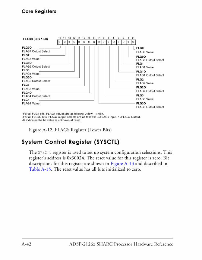
Core Registers
A-42 ADSP-2126x SHARC Processor Hardware Reference
System Control Register (SYSCTL)The SYSCTL register is used to set up system configuration selections. This register’s address is 0x30024. The reset value for this register is zero. Bit descriptions for this register are shown in Figure A-13 and described in Table A-15. The reset value has all bits initialized to zero.
Figure A-12. FLAGS Register (Lower Bits)
15 14 13 12 11 10 9 8 7 6 5 4 3 2 1 0
U0 U 0 U 0 U 0 U 0 U 0 U 0 U 0
FLG7OFLAG7 Output SelectFLG7FLAG7 ValueFLG6OFLAG6 Output SelectFLG6FLAG6 ValueFLG5OFLAG5 Output SelectFLG5FLAG5 ValueFLG4OFLAG4 Output SelectFLG4FLAG4 Value
FLG0FLAG0 Value
FLG0OFLAG0 Output SelectFLG1FLAG1 Value
FLG1OFLAG1 Output Select
FLG2FLAG2 Value
FLG2OFLAG2 Output Select
FLG3FLAG3 Value
FLG3OFLAG3 Output Select
-For all FLGx bits, FLAGx values are as follows: 0=low, 1=high.-For all FLGxO bits, FLAGx output selects are as follows: 0=FLAGx Input, 1=FLAGx Output.-U indicates the bit value is unknown at reset.
FLAGS (Bits 15-0)

ADSP-2126x SHARC Processor Hardware Reference A-43
Registers Reference
Figure A-13. SYSCTL Register
Table A-15. SYSCTL Register Bit Descriptions
Bits Name Definition
0 SRST Software Reset. Resets (when set, = 1) the processor. When a program sets (= 1) SRST, the processor responds to the non-maskable RSTI interrupt and clears (= 0) SRST.
1 Reserved
15 14 13 12 11 10 9 8 7 6 5 4 3 2 1 0
00 0 0 0 0 0 0 0 0 0 0 0 0 0 0
SRST
IMDW0
IMDW1
Reserved
Internal Memory Block 1 Data Width1=Data bus width is 48 bits0=Data bus is 32 bits
Software Reset1=Disable0=Enable (permits core writes)
IRQ0EN
TMREXPEN
PPFLGS
Reserved
Parallel Port Mode Enable1=Enable0=Disable Parallel Port. ADDR pins are FLAGS (permits core writes)
Flag3 Mode1=FLAG3 is in TIMEXP mode0=FLAG3 is in FLAG3 mode (permits core writes)
Flag0 Mode1=FLAG0 is in IRQ0 mode0=FLAG0 is in FLAG0 mode (permits core writes)
IRQ1EN
Flag1 Mode1=FLAG1 is in IRQ1 mode0=FLAG1 is in FLAG1 mode (permits core writes)
IRQ2ENFlag2 Mode1=FLAG2 is in IRQ2 mode0=FLAG2 is in FLAG2 mode (permits core writes)
Internal Memory Block 0 Data Width1=Data bus width is 48 bits0=Data bus is 32 bits
Reserved
Reserved
IIVT
Internal Interrupt Vector Table1=Interrupt Vector Table is in internal RAM0=Interrupt Vector Table is not in internal RAM (permits core reads)
ReservedDCPR
Priority Bit Enable1=Rotating priority0=Fixed priority (permits core writes)
SYSCTL (0x30024)31 30 29 28 27 26 25 24 23 22 21 20 19 18 17 16
00 0 0 0 0 0 0 0 0 0 0 0 0 00

Core Registers
A-44 ADSP-2126x SHARC Processor Hardware Reference
2 IIVT Internal Interrupt Vector Table. Forces placement of the inter-rupt vector table at address 0x0008 0000 regardless of booting mode (if 1) or allows placement of the interrupt vector table as selected by the booting mode (if 0).
6–3 Reserved
7 DCPR DMA Channel Priority Rotation Enable. Enables (rotates if set, = 1) or disables (fixed if cleared, = 0) priority rotation among DMA channels. Permits core writes.
8 Reserved
9 IMDW0 Internal Memory Data Width 0. Selects the data access size for internal memory as 48-bit data if set, (= 1) or 32-bit data if cleared, (= 0). Permits core writes.
10 IMDW1 Internal Memory Data Width 1. Selects the data access size for internal memory as 48-bit data if set, (= 1) or 32-bit data if cleared, (= 0). Permits core writes.
15–11 Reserved
16 IRQ0EN Flag0 Interrupt Mode. 1 = Flag0 pin is allocated to interrupt request IRQ0. 0 = Flag0 pin is a general purpose I/O pin. Permits core writes.
17 IRQ1EN Flag1 Interrupt Mode.1 = Flag1 pin is allocated to interrupt request IRQ1.0 = Flag1 pin is a general purpose I/O pin. Permits core writes.
18 IRQ2EN Flag2 Interrupt Mode.1 = Flag2 pin is allocated to interrupt request IRQ2.0 = Flag2 pin is a general purpose I/O pin. Permits core writes.
19 TMREXPEN Flag Timer Expired Mode. Read/Write 1 = Flag3 pin outputs are timer-expired signal (TIMEXP).0 = Flag3 pin is a general purpose I/O pin.Permits core writes.
Table A-15. SYSCTL Register Bit Descriptions (Cont’d)
Bits Name Definition

ADSP-2126x SHARC Processor Hardware Reference A-45
Registers Reference
Emulation Registers
Hardware Breakpoint Control Register (BRKCTL)
The BRKCTL register controls how breakpoints are used (if the UMODE bit is set). This user-accessible register in the BRKCTL register is located at address 0x30025.
The BRKCTL register is a 32-bit memory-mapped I/O register. The proces-sor core can write into this register. The bits related to the breakpoint register are same as in the EMUCTL register.
20 PPFLGS Parallel Port Select.0 = Parallel port is selected.1 = Parallel port is not selected. ADDR and DATA pins are in FLAG mode. Permits core writes. Configuring the parallel port pins to function as FLAG0-15 also causes the FLAG[0:3] pins to change to their alternate role, IRQ0-2 and TIMEXP.
31–21 Reserved
Table A-15. SYSCTL Register Bit Descriptions (Cont’d)
Bits Name Definition

Core Registers
A-46 ADSP-2126x SHARC Processor Hardware Reference
Figure A-14. BRKCTL Register (Upper Bits)
31 30 29 28 27 26 25 24 23 22 21 20 19 18 17 16
00 0 0 0 0 0 0 0 0 0 0 0 0 0 0
NEGIA4
UMODE
IODISABLEReserved
Disable I/O Breakpoints00=Breakpoint Disabled01=WRITE Access10=READ Access11=Any Access
Enable User Mode BreakpointAddress Breakpoint #31=Enable Breakpoint0=Disable Breakpoint
Negate Instruction Address Breakpoint #41=Enable Breakpoint0=Disable Breakpoint
ANDBKPAND Composite Breakpoints1=AND Breakpoint Types0=OR Breakpoint Types
Reserved
Enable Instruction Address Breakpoints (See ENBPA bit description)
ENBIA
NEGIO1Negate I/O Address Breakpoint #11=Enable Breakpoint0=Disable Breakpoint
ENBPAEnable Program Memory Address Breakpoints1=Enable Breakpoint0=Disable Breakpoint
ENBDAEnable Data Memory Breakpoints1=Enable Breakpoint0=Disable Breakpoint
BRKCTL (Bits 31-16)

ADSP-2126x SHARC Processor Hardware Reference A-47
Registers Reference
Figure A-15. BRKCTL Register (Lower Bits)
Table A-16. BRKCTL Register Bit Descriptions
Bit # Name Function
1–0 PA1MODE PA1Triggering Mode00 = Breakpoint Disabled01 = WRITE Access10 = READ Access11 = Any access
3–2 DA1MODE DA1 Triggering Mode00 = Breakpoint Disabled01 = WRITE Access10 = READ Access11 = Any access
15 14 13 12 11 10 9 8 7 6 5 4 3 2 1 0
10 0 0 0 0 0 0 0 0 0 0 0 0 0 0
NEGIA3Negate Instruction Address Breakpoint #31=Enable Breakpoint0=Disable Breakpoint
PA1MODEPA1 Triggering Mode00=Breakpoint Disabled01=WRITE Access10=READ Access11=Any AccessNEGIA2
Negate Instruction Address Breakpoint #21=Enable Breakpoint0=Disable Breakpoint
NEGIA1Negate Instruction Address Breakpoint #11=Enable Breakpoint0=Disable Breakpoint
NEGDA2Negate DM Address Breakpoint #21=Enable Breakpoint0=Disable Breakpoint
NEGDA1Negate DM Address Breakpoint #11=Enable Breakpoint0=Disable Breakpoint
DA1MODEDA1 Triggering Mode00=Breakpoint Disabled01=WRITE Access10=READ Access11=Any Access
DA2MODEDA2 Triggering Mode00=Breakpoint Disabled01=WRITE Access10=READ Access11=Any Access
IO1MODEIO1 Triggering Mode00=Breakpoint Disabled01=WRITE Access10=READ Access11=Any Access
NEGPA1Negate PM Address Breakpoint #11=Enable Breakpoint0=Disable Breakpoint
BRKCTL (0x30025)(Bits 15-0)

Core Registers
A-48 ADSP-2126x SHARC Processor Hardware Reference
5–4 DA2MODE DA2 Triggering Mode00 = Breakpoint Disabled01 = WRITE Access10 = READ Access11 = Any Access
7–6 IO1MODE IO1 Triggering Mode trigger on the following conditions:Mode Triggering condition00 = Breakpoint is disabled01 = WRITE accesses only10 = READ accesses only11 = Any access
9–8 Reserved
10 NEGPA1 Negate Program Memory Data Address BreakpointEnable breakpoint events if the address is greater than the end register value OR less than the start register value. This function is useful to detect index range violations in user code. 0 = Disable Breakpoint1 = Enable Breakpoint
11 NEGDA1 Negate Data Memory Address Breakpoint #1For more information, see NEGPA1 bit description.
12 NEGDA2 Negate Data Memory Address Breakpoint #2For more information, see NEGPA1 bit description.
13 NEGIA1 Negate Instruction Address Breakpoint #10 = Disable Breakpoint1 = Enable Breakpoint
14 NEGIA2 Negate Instruction Address Breakpoint #2For more information, see NEGPA1 bit description.
15 NEGIA3 Negate Instruction Address Breakpoint #3For more information, see NEGPA1 bit description.
16 NEGIA4 Negate Instruction Address Breakpoint #4For more information, see NEGPA1 bit description.
17 NEGIO1 Negate I/O Address BreakpointFor more information, see NEGPA1 bit description.
18 Reserved
Table A-16. BRKCTL Register Bit Descriptions (Cont’d)
Bit # Name Function

ADSP-2126x SHARC Processor Hardware Reference A-49
Registers Reference
Emulation Control (EMUCTL) Register
The EMUCTL Serial Shift register is located in the system unit. The EMUCTL register is 40 bits wide and is accessed by the emulator through the TAP. The EMUCTL register controls all of the ADSP-2126x emulation functional-ity. Table A-17 lists the EMUCTL register’s bits and describes their function.
19 ENBPA Enable Program Memory Data Address BreakpointsThe ENB* bits enable each breakpoint group. Note that when the ANDBKP bit is set, breakpoint types not involved in the generation of the effective breakpoint must be disabled. 0 = Disable Breakpoints1 = Enable Breakpoints
20 ENBDA Enable Data Memory Address BreakpointsFor more information, see ENBPA bit description.
21 ENBIA Enable Instruction Address Breakpoints.For more information, see ENBPA bit description.
23–22 Reserved
24 ANDBKP AND composite breakpoints Enables ANDing of each break-point type to generate an effective breakpoint from the compos-ite breakpoint signals.0 = OR Breakpoint Types1 = AND Breakpoint Types
25 UMODE User Mode Breakpoint Functionality Enable Address Breakpoint 30 = Disable Breakpoint1 = Enable Breakpoint
27–26 IODISABLE Enable I/O Breakpoints00 = Breakpoint Disabled01 = WRITE Access10 = READ Access11 = Any Access
31–28 Reserved
Table A-16. BRKCTL Register Bit Descriptions (Cont’d)
Bit # Name Function

Core Registers
A-50 ADSP-2126x SHARC Processor Hardware Reference
Table A-17. Emulation Control Register (EMUCTL) Definitions
Bit # Name Function
0 EMUENA Emulator Function Enable. Enables processor emulation func-tions. (0 = ignore breakpoints and emulator interrupts, 1=respond
to breakpoints and emulator interrupts)
1 EIRQENA Emulator Interrupt Enable. Enables the emulation logic to recog-
nize external emulator interrupts. (0 = disable, 1 = enable)
2 BKSTOP Enable Autostop on Breakpoint. Enables the ADSP-2126x DSP to generate an external emulator interrupt when any breakpoint event occurs. (0=disable, 1=enable)
3 SS Enable Single Step Mode. Enables single-step operation.
(0=disable, 1=enable)
4 SYSRST Software Reset of the ADSP-2126x. Resets the ADSP-2126x DSP in the same manner as the external RESET pin. The SYSRST bit
must be cleared by the emulator.(0=normal operation, 1=reset)
5 ENBRKOUT Enable the BRKOUT pin. Enables the BRKOUT pin operation.
(0 = BRKOUT pin at high impedance state, 1 = BRKOUT pin enabled)
6 IOSTOP Stop IOP DMAs in EMU Space. Disables all DMA requests when the DSP is in emulation space. Data that is currently in the SPI or SPORT DMA buffers is held there unless the internal DMA request was already granted. IOSTOP causes incoming data to be held off and outgoing data to cease. Because SPORT receive data cannot be held off, it is lost and the overrun bit is set.
(0 = I/O continues, 1 = I/O Stops)
7 Reserved
8 NEGPA1 Negate program memory data address breakpoint. Enable break-point events if the address is greater than the end register value OR less than the start register value. This function is useful to detect index range violations in user code.(0 = disable breakpoint, 1 = enable breakpoint)Instruction address and program memory breakpoint negates have an effect latency of four (4) core clock cycles.

ADSP-2126x SHARC Processor Hardware Reference A-51
Registers Reference
9 NEGDA1 Negate data memory address breakpoint #1 see NEGPA1 bit
description.
10 NEGDA2 Negate data memory address breakpoint #2 see NEGPA1 bit
description.
11 NEGIA1 Negate instruction address breakpoint #1 see NEGPA1 bit
description.
12 NEGIA2 Negate instruction address breakpoint #2. see NEGPA1 bit
description.
13 NEGIA3 Negate instruction address breakpoint #3 see NEGPA1 bit
description.
14 NEGIA4 Negate instruction address breakpoint #4 see NEGPA1 bit
description.
15 NEGIO1 Negate I/O address breakpoint see NEGPA1 bit description.
16 NEGEP1 Negate EP address breakpoint see NEGPA1 bit description.
17 ENBPA Enable program memory data address breakpoints. Enable each breakpoint group. Note that when the ANDBKP bit is set, break-point types not involved in the generation of the effective break-point must be disabled. (0 = disable breakpoints, 1 = enable
breakpoints)
18 ENBDA Enable data memory address breakpoints see ENBPA bit descrip-
tion.
19 ENBIA Enable instruction address breakpoints see ENBPA bit descrip-
tion.
20–21 Reserved
Table A-17. Emulation Control Register (EMUCTL) Definitions (Cont’d)
Bit # Name Function
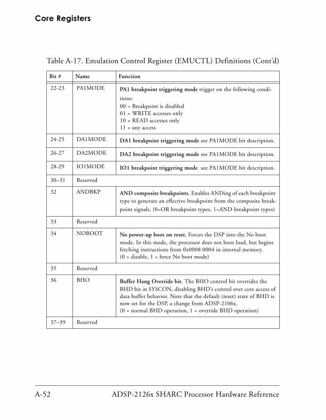
Core Registers
A-52 ADSP-2126x SHARC Processor Hardware Reference
22-23 PA1MODE PA1 breakpoint triggering mode trigger on the following condi-
tions:00 = Breakpoint is disabled01 = WRITE accesses only10 = READ accesses only11 = any access
24-25 DA1MODE DA1 breakpoint triggering mode see PA1MODE bit description.
26-27 DA2MODE DA2 breakpoint triggering mode see PA1MODE bit description.
28-29 IO1MODE IO1 breakpoint triggering mode see PA1MODE bit description.
30–31 Reserved
32 ANDBKP AND composite breakpoints. Enables ANDing of each breakpoint type to generate an effective breakpoint from the composite break-
point signals. (0=OR breakpoint types, 1=AND breakpoint types)
33 Reserved
34 NOBOOT No power-up boot on reset. Forces the DSP into the No boot mode. In this mode, the processor does not boot load, but begins fetching instructions from 0x0008 0004 in internal memory.(0 = disable, 1 = force No boot mode)
35 Reserved
36 BHO Buffer Hang Override bit. The BHO control bit overrides the BHD bit in SYSCON, disabling BHD’s control over core access of data buffer behavior. Note that the default (reset) state of BHD is now set for the DSP, a change from ADSP-2106x. (0 = normal BHD operation, 1 = override BHD operation)
37–39 Reserved
Table A-17. Emulation Control Register (EMUCTL) Definitions (Cont’d)
Bit # Name Function

ADSP-2126x SHARC Processor Hardware Reference A-53
Registers Reference
Breakpoint (PSx, DMx, IOx) Registers
The PSx, DMx, IOx (Breakpoint) registers are located in the I/O processor register set. The emulation breakpoint registers are user-accessible if the UMODE bit is set in the BRKCTL register. Otherwise they can be written only when the DSP is in emulation space or test mode. The Breakpoint regis-ters vary in size according to the address type: instruction (24-bit address), data (32-bit address), or I/O data (19-bit address).
The ADSP-2126x contains nine sets of emulation Breakpoint registers. Each set consists of a start and end register which describe an address range, with the start register setting the lower end of the address range. Each breakpoint set monitors a particular address bus. When a valid address is in the address range, then a breakpoint signal is generated. The address range includes the start and end addresses.
The eight breakpoint sets are grouped into four types—instruction (IA), DM data (DA), PM data (PA), and I/O data (I/O). The individual break-point signals in each type are ORed together to create five composite breakpoint signals.
These composite signals can be optionally ANDed or ORed together to create the effective breakpoint event signal used to generate an emulator interrupt. The ANDBKP bit in the EMUCTL register selects the function used.
Each breakpoint type has an enable bit in the EMUCTL register. When set, these bits add the specified breakpoint type into the generation of the effective breakpoint signal. If cleared, the specified breakpoint type is not used in the generation of the effective breakpoint signal. This allows the user to trigger the effective breakpoint from a subset of the breakpoint types.
To provide further flexibility, each individual breakpoint can be pro-grammed to trigger if the address is in range AND one of these conditions is met: READ access, WRITE access, ANY access, or NO access. The con-trol bits for this feature are also located in EMUCTL register. For more information, see the PA1MODES bit description.

Core Registers
A-54 ADSP-2126x SHARC Processor Hardware Reference
The address ranges of the emulation Breakpoint registers are negated by setting the appropriate negation bits in the EMUCTL register. For more information, see the NEGPA1 bit description. Each breakpoint can be dis-abled by setting the start address larger than the end address.
Four of the breakpoints monitor the instruction address. Two monitor the data memory address. One monitors the program memory data address, and one monitors the I/O address bus.
The instruction address breakpoints monitor the address of the instruc-tion being executed, not the address of the instruction being fetched. If the current execution is aborted, the breakpoint signal does not occur even if the address is in range. Data address breakpoints (DA and PA only) are also ignored during aborted instructions. The nine breakpoint sets appear in Table A-18.
Table A-18. PSx, DMx, IOx, and EPx (Breakpoint) Registers
Register Function Group1
PSA1S Instruction Address Start #1 IA
PSA1E Instruction Address End #1 IA
PSA2S Instruction Address Start #2 IA
PSA2E Instruction Address End #2 IA
PSA3S Instruction Address Start #3 IA
PSA3E Instruction Address End #3 IA
PSA4S Instruction Address Start #4 IA
PSA4E Instruction Address End #4 IA
DMA1S Data Address Start #1 DA
DMA1E Data Address End #1 DA
DMA2S Data Address Start #2 DA
DMA2E Data Address End #2 DA

ADSP-2126x SHARC Processor Hardware Reference A-55
Registers Reference
PMDAS Program Data Address Start PA
PMDAE Program Data Address End PA
IOAS I/O Address Start I/O
IOAE I/O Address End I/O
1 Group IA = 24-bit addresses, Groups DA and PA = 32-bit addresses, Group I/O = 19-bit addresses.
Table A-19. EEMUSTAT (Breakpoint Status) Register Definitions
Bits Name Function
0 STATPA Program memory Data Breakpoint Hit1
1 = Program memory breakpoint occurs0 = No program memory breakpoint occurs
1 STATDA0 Data Memory Breakpoint Hit1
1 = Data memory #0 breakpoint occurs0 = No data memory #0 breakpoint occurs
2 STATDA1 Data Memory Breakpoint Hit1
1 = Data memory #1 breakpoint occurs0 = No Data memory #1 breakpoint occurs
3 STATIA0 Instruction Address Breakpoint Hit1
1 = Instruction address #0 breakpoint occurs0 = no Instruction address #0 breakpoint occurs
4 STATIA1 Instruction Address Breakpoint Hit1
1 = Instruction address #1 breakpoint occurs0 = no Instruction address #1 breakpoint occurs
5 STATIA2 Instruction Address Breakpoint Hit1
1 = Instruction address #2 breakpoint occurs0 = no Instruction address #2 breakpoint occurs
Table A-18. PSx, DMx, IOx, and EPx (Breakpoint) Registers (Cont’d)
Register Function Group1

Core Registers
A-56 ADSP-2126x SHARC Processor Hardware Reference
6 STATIA3 Instruction Address Breakpoint Hit1
1 = Instruction address #3 breakpoint occurs0 = no Instruction address #3 breakpoint occurs
7 STATIO I/O Address Breakpoint Hit1 = I/O address breakpoint occurs0 = no I/O address breakpoint occurs
8 Reserved1
9 EEMU-OUTIRQEN
Enhanced Emulation EEMUOUT Interrupt Enable2
1 = EEMUOUT interrupt enable0 = EEMUOUT interrupt disableNote: Interrupts are of low priority interrupts
10 EEMUOUTRDY Enhanced Emulation EEMUOUT Ready3
1 = EEMUOUT FIFO contains valid data0 = EEMUOUT FIFO is empty
11 EEMUOUTFULL Enhanced Emulation EEMUOUT FIFO Status3
1 = EEMUOUT FIFO FULL0 = EEMUOUT FIFO is not FULL
12 EEMUINFULL Enhanced Emulation EEMUIN Register Status4
1 = EEMUIN register full0 = EEMUIN register is empty
13 EEMUENS Enhanced Emulation Feature Enable4
1 = Enhanced emulation feature enable0 = Enhanced emulation feature disable
14 OSPIDENS OSPID Register Enable4
1 = OSPID register enable0 = OSPID register disable
15 EEMUINENS EEMUIN Interrupt Enable.1 = EEMUIN interrupt enable0 = EEMUIN interrupt disable
31:16 Reserved for future use.
1 Internal hardware sets this bit.
Table A-19. EEMUSTAT (Breakpoint Status) Register Definitions
Bits Name Function

ADSP-2126x SHARC Processor Hardware Reference A-57
Registers Reference
EEMUIN Register
The EEMUIN register is a one-deep, 32-bit memory-mapped I/O buffer that is readable by the core. This buffer is used by the background telemetry channel to allow the emulator to pass data to the DSP without interrupt-ing the core. When this buffer is full, a low priority emulator interrupt is generated. This register’s address is 0x30020.
Enhanced Emulation Status Register (EEMUSTAT)
The EEMUSTAT register reports the breakpoint status of the programs that run on the SHARC processors. This register is a memory-mapped IOP register that can be accessed by the core. The bit settings for these registers are shown in Figure A-16.
2 This bit is set and reset by the core.3 The FIFO controller sets and resets this bit.4 Internal hardware sets and resets this bit.

Core Registers
A-58 ADSP-2126x SHARC Processor Hardware Reference
Figure A-16. EEMUSTAT Register
Table A-20. EEMUSTAT Register Bit Descriptions
Bit Name Description
0 STATPA Program Memory Data Breakpoint Hit.1
0 = No program memory breakpoint occurs1 = Program memory breakpoint occurs
1 STATDA0 Data Memory Breakpoint Hit.1
0 = No data memory #0 breakpoint occurs1 = Data memory #0 breakpoint occurs
2 STATDA1 Data Memory Breakpoint Hit.1
0 = No data memory #1 breakpoint occurs1 = Data memory #1 breakpoint occurs
15 14 13 12 11 10 9 8 7 6 5 4 3 2 1 0
00 0 0 0 0 0 0 0 0 0 0 0 0 0 0
EEMUIN Interrupt EnableEEMUINENS
EEMUENSEnhanced Emulation Feature Enable Status
EEMUINFULL
EEMUOUTFULL
EEMUIN FIFO Full Status
EEMUOUTRDYEEMUOUT FIFO Full Status
EEMUOUT Valid Data Status
EEMUOUTIRQENEEMUOUT Interrupt Enable
STATPAProgram Memory Break-point Status
STATDA0DM Breakpoint #0 StatusSTATDA1DM Breakpoint #1 StatusSTATIA0Instruction Breakpoint #0 StatusSTATIA1Instruction Breakpoint #1 StatusSTATIA2Instruction Breakpoint #2 StatusSTATIA3Instruction Breakpoint #3 Status
STATIO0DMA Peripheral Address Break-point Status
31 30 29 28 27 26 25 24 23 22 21 20 19 18 17 16
00 0 0 0 0 0 0 0 0 0 0 0 0 0 0
STATIO1DMA EP Address Breakpoint Status

ADSP-2126x SHARC Processor Hardware Reference A-59
Registers Reference
3 STATIA0 Instruction Address Breakpoint Hit.1
0 = No instruction address #0 breakpoint occurs1 = Instruction address #0 breakpoint occurs
4 STATIA1 Instruction Address Breakpoint Hit.1
0 = No instruction address #1 breakpoint occurs1 = Instruction address #1 breakpoint occurs
5 STATIA2 Instruction Address Breakpoint Hit.1
0 = No instruction address #2 breakpoint occurs1 = Instruction address #2 breakpoint occurs
6 STATIA3 Instruction Address Breakpoint Hit.1
0 = No instruction address #3 breakpoint occurs1 = Instruction address #3 breakpoint occurs
7 STATIO0 DMA Peripheral Address Breakpoint Status.1 Set bit if breakpoint hit detected on the IOD/IOD0 bus0 = No DMA peripheral address breakpoint occurs1 = DMA peripheral address breakpoint occurs
8 Reserved
9 EEMUOUTIRQEN Enhanced Emulation EEMUOUT Interrupt Enable.2
0 = EEMUOUT interrupt disable1 = EEMUOUT interrupt enableNote: Interrupts are of the low priority variety
10 EEMUOUTRDY Enhanced Emulation EEMUOUT Ready.3
1 = EEMUOUT FIFO contains valid data0 = EEMUOUT FIFO is empty
11 EEMUOUTFULL Enhanced Emulation EEMUOUT FIFO Status.3
0 = EEMUOUT FIFO is not full1 = EEMUOUT FIFO full
12 EEMUINFULL Enhanced Emulation EEMUIN Register Status.4
0 = EEMUIN register is empty1 = EEMUIN register full
Table A-20. EEMUSTAT Register Bit Descriptions (Cont’d)
Bit Name Description

Core Registers
A-60 ADSP-2126x SHARC Processor Hardware Reference
EEMUOUT Register
The EEMUOUT register is a four-deep memory, 32-bit memory-mapped I/O buffer that is writable by the core. Its address is 0x30022.
Emulation Clock Counter Registers
The EMUCLK (clock counter) and EMUCLK2 (clock counter scaling) registers are located in the Universal (Ureg) register set. EMUCLK and EMUCLK2 regis-ters are user accessible and can be written only when the DSP is in emulation space. These registers are read-only from normal-space and can be written only when the ADSP-2126x is in emulation space. The Emula-tion Clock Counter consists of a 32-bit Count register (EMUCLK) and a 32-bit scaling register (EMUCLK2). The EMUCLK register counts clock cycles
13 EEMUENS Enhanced Emulation Feature Enable.4
0 = Enhanced emulation feature enable1 = Enhanced emulation feature disable
14 Reserved
15 EEMUINENS EEMUIN Interrupt Enable.4
0 = EEMUIN interrupt disable1 = EEMUIN interrupt enable
16 STATIO1 DMA EP Address Breakpoint Status. Set bit if breakpoint hit detected on the IOD1 bus (between EP and internal memory)0 = No EP DMA breakpoint occurs 1 = EP DMA Breakpoint occurs(reserved for ADSP-21362/3/4/5/6 processors)
31–17 Reserved
1 Internal hardware sets this bit.2 This bit is set and reset by the core.3 The FIFO controller sets and resets this bit.4 Internal hardware sets and resets this bit.
Table A-20. EEMUSTAT Register Bit Descriptions (Cont’d)
Bit Name Description

ADSP-2126x SHARC Processor Hardware Reference A-61
Registers Reference
while the user has control of the DSP and stops counting when the emula-tor gains control. These registers let you gauge the amount of time spent executing a particular section of code. The EMUCLK2 register extends the time EMUCLK can count by incrementing each time the EMUCLK value rolls over to zero. The combined emulation clock counter can count accurately for thousands of hours.
I/O Processor RegistersThe I/O Processor (IOP) registers are accessible as part of the processor’s memory map. Table A-21 on page A-62 lists the IOP memory-mapped registers and provides a cross-reference to a description of each register. These registers occupy addresses 0x0000 0000 through 0x0003 FFFF of the memory map. The IOP memory-mapped space is sub divided into peripheral and core memory mapped registers. The IOP registers control the following operations: Parallel port, Serial port, Serial Peripheral Inter-face port (SPI), and Input Data port (IDP).
IOP registers have a one cycle effect latency (changes take effect on the second cycle after the change).
Since the IOP registers are part of the processor’s memory map, buses access these registers as locations in memory. While these registers act as memory-mapped locations, they are separate from the processor’s internal memory and have different bus access. One bus can access one IOP regis-ter group at a time. Table A-21 on page A-62 lists the IOP register groups.
When there is contention among the buses for access to registers, the pro-cessor arbitrates register access as:
• Data Memory (DM) bus accesses
• Program Memory (PM) bus accesses
• IOP (IO) bus (lowest priority) accesses

I/O Processor Registers
A-62 ADSP-2126x SHARC Processor Hardware Reference
The bus with highest priority gets access to the IOP register, and the other buses are held off from accessing that I/O processor register group until that access been completed.
Table A-21. I/O Processor Registers
Register Group IOP Registers
Core I/O Registers SYSCTL, REVPID, EEMUIN, EEMUSTAT, EEMUOUT, OSPID, BRKCTL, PSA1S, PSA1E, PSA2S, PSA2E, PSA3S, PSA3E, PSA4S, PSA4E, DMA1S, DMA1E, DMA2S, DMA2E, PMDAS, PMDAE, EMUN, IOAS, IOAE
Parallel Port (PP) Regis-ters
PPCTL, RXPP, TXPP, EIPP, EMPP, ECPP, IIPP, IMPP, ICPP
Serial Peripheral Interface (SPI) Registers
RXSPI, SPIFLG, TXSPI, SPICTL, SPISTAT, SPIBAUD, SPIDMAC, IISPI, IMSPI, RXSPI_SHADOW, CPSPI, CSPI
Timer Registers TM0STAT, TM0CTL, TM0CNT, TM0PRD, TM0W, TM1STAT, TM1CTL, TM1CNT, TM1PRD, TM1W, TM2STAT, TM2CTL, TM2CNT, TM2PRD, TM2W
Power Management Registers
PMCTL

ADSP-2126x SHARC Processor Hardware Reference A-63
Registers Reference
Since the I/O processor registers are memory-mapped, the processor’s architecture does not allow programs to directly transfer data between
Serial Port (SP)Registers
IISP0A, IISP0B, IMSP0A, IMSP0B, CSP0A, CSP0B, CPSP0A, CPSP0B, IISP1A, IISP1B, IMSP1A, IMSP1B, CSP1A, CSP1B, CPSP1A, CPSP1B, IISP2A, IISP2B, IMSP2A, IMSP2B, CSP2A, CSP2B, CPSP2A, CPSP2B, IISP3A, IISP3B, IMSP3A, IMSP3B, CSP3A, CSP3B, CPSP3A, CPSP3B, IISP4A, IISP4B, IMSP4A, IMSP4B, CSP4A, CSP4B, CPSP4A, CPSP4B, IISP5A, IISP5B, IMSP5A, IMSP5B, CSP5A, CSP5B, CPSP5A, CPSP5BRXSP0A, RXSP0B, TXSP0A, TXSP0B, SPCTL0, DIV0, MT0CS0, MT0CCS0, MT0CS1, MT0CCS1, MT0CS2, MT0CCS2, MT0CS3, MT0CCS3RXSP1A, RXSP1B, TXSP1A, TXSP1B, SPCTL1, DIV1, MR1CS0, MR1CCS0, MR1CS1, MR1CCS1, MR1CS2, MR1CCS2, MR1CS3, MR1CCS3RXSP2A, RXSP2B, TXSP2A, TXSP2B, SPCTL2, DIV2, MT2CS0, MT2CCS0, MT2CS1, MT2CCS1, MT2CS2, MT2CCS2, MT2CS3, MT2CCS3RXSP3A, RXSP3B, TXSP3A, TXSP3B, SPCTL3, DIV3, MR3CS0, MR3CCS0, MR3CS1, MR3CCS1, MR3CS2, M3CCS2, MR3CCS2, MR3CS3, MR3CCS3RXSP4A, RXSP4B, TXSP4A, TXSP4B, SPCTL4, DIV4, MT4CS0, MT4CCS0, MT4CS1, MT4CCS1, MT4CS2, MT4CCS2, MT4CS3, MT4CCS3RXSP5A, RXSP5B, TXSP5A, TXSP5B, SPCTL5, DIV5, MR5CS0, MR5CCS0, MR5CS1, MR5CCS1, MR5CS2, MR5CCS2, MR5CS3, MR5CCS3SPMCTL01, SPMCTL23, SPMCTL45
DAI Registers SRU_CLK0, SRU_CLK1, SRU_CLK2, SRU_CLK3SRU_DAT0, SRU_DAT1, SRU_DAT2, SRU_DAT3, SRU_DAT4SRU_FS0, SRU_FS1, SRU_FS2SRU_PIN0, SRU_PIN1, SRU_PIN2, SRU_PIN3SRU_EXT_MISCA, SRU_EXT_MISCBSRU_PBEN0, SRU_PBEN1, SRU_PBEN2, SRU_PBEN3PCG_CTLA_0, PCG_CTLA_1, PCG_CTLB_0, PCG_CTLB_1, PCG_PWIDP_CTL, DAI_STAT, IDP_FIFO, IDP_DMA_I0, IDP_DMA_I1, IDP_DMA_I2, IDP_DMA_I3, IDP_DMA_I4, IDP_DMA_I5, IDP_DMA_I6, IDP_DMA_I7, IDP_DMA_M0, IDP_DMA_M1, IDP_DMA_M2, IDP_DMA_M3, IDP_DMA_M4, IDP_DMA_M5, IDP_DMA_M6, IDP_DMA_M7, IDP_DMA_C0, IDP_DMA_C1, IDP_DMA_C2, IDP_DMA_C3, IDP_DMA_C4, IDP_DMA_C5, IDP_DMA_C6, IDP_DMA_C7, IDP_PP_CTLDAI_PIN_PULLUP, DAI_PIN_STAT, DAI_IRPTL_H, DAI_IRPTL_L, DAI_IRPTL_PRI, DAI_IRPTL_RE, DAI_IRPTL_FE
Table A-21. I/O Processor Registers (Cont’d)
Register Group IOP Registers

I/O Processor Registers
A-64 ADSP-2126x SHARC Processor Hardware Reference
these registers and other memory locations, except as part of a DMA oper-ation. To read or write IOP registers, programs must use the processor core registers.
The register names for IOP registers are not part of the processor’s assem-bly syntax. To ease access to these registers, programs should use the header file containing the registers’ symbolic names and addresses as described on page A-61.
Power Management RegistersThe following sections describe the registers associated with the DSPs power management functions.
Power Management Control Register (PMCTL)
The Power Management Control register is a 32-bit memory-mapped reg-ister. The PMCTL register’s addresses is 0x2000. This register contains bits to control phase lock loop (PLL) multiplier and Divider (both input and output) values, PLL bypass mode, and clock enabling control for peripher-als (see Table A-22). This register also contains status bits, which keep track of the status of the CLK_CFG pins (read-only).
The core can write to all bits except the read-only status bits. The DIVEN bit is a logical bit, that is, it can be set, but on reads it always responds with zero.
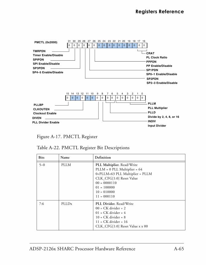
ADSP-2126x SHARC Processor Hardware Reference A-65
Registers Reference
Figure A-17. PMCTL Register
Table A-22. PMCTL Register Bit Descriptions
Bits Name Definition
5–0 PLLM PLL Multiplier. Read/WritePLLM = 0 PLL Multiplier = 640<PLLM<63 PLL Multiplier = PLLMCLK_CFG[1:0] Reset Value00 = 000011001 = 10000010 = 01000011 = 000110
7:6 PLLDx PLL Divider. Read/Write00 = CK divider = 201 = CK divider = 410 = CK divider = 811 = CK divider = 16CLK_CFG[1:0] Reset Value x x 00
31 30 29 28 27 26 25 24 23 22 21 20 19 18 17 16
00 0 0 0 0 0 0 0 0 0 0 0 0 0 0
15 14 13 12 11 10 9 8 7 6 5 4 3 2 1 0
00 0 0 0 0 0 0 0 0 0 0 0 0 0 0
TMRPDN
PLLBP
Timer Enable/Disable
CLKOUTENClockout Enable
DIVEN
CRATPL Clock Ratio
PLLM
PLL Multiplier
SPIPDNSPI Enable/Disable
SP3PDN
SP2PDNSP2–3 Enable/Disable
PPPDNPP Enable/DisableSP1PDNSP0–1 Enable/Disable
PLL Divider Enable
PLLD
Divide by 2, 4, 8, or 16
INDIV
Input Divider
PMCTL (0x2000)
SP4–5 Enable/Disable

I/O Processor Registers
A-66 ADSP-2126x SHARC Processor Hardware Reference
8 INDIV Input Divisor. Read/Write0 = divide by 11 = divide by 2Reset Value = 0
9 DIVEN Enable PLL Divider Value Loading. Read/Write0 = Do not load PLLDx1 = Load PLLDxReset Value = 0
11–10 Reserved
12 CLKOUTEN Clockout Enable. Read/Write (Use for debug only)Mux select for CLKOUT and RESETOUT0 Mux output = RESETOUT1 Mux output = CLKOUTReset Value = 0
14–13 Reserved
15 PLLBP PLL Bypass Mode Indication. Read/Write0 = PLL is in normal mode1 = Put PLL in bypass modeReset Value = 0
17:16 CRAT PLL clock ratio (CLKIN to CK). Read only. For more detail look for refer to the ADSP-2126x clock configura-tion pin description.Reset Value = CLK_CFG[1:0]
25–18 Reserved
26 PPPDN PP Enable/Disable. Read/Write0 = PP is in normal mode1 = Shutdown clock to PPReset Value = 0
27 SP1PDN SP1 Enable/Disable. Read/Write0 = SP0–1 are in normal mode1 = Shutdown clock to SP0–1Reset Value = 0
Table A-22. PMCTL Register Bit Descriptions (Cont’d)
Bits Name Definition

ADSP-2126x SHARC Processor Hardware Reference A-67
Registers Reference
28 SP2PDN SP2 Enable/Disable. Read/Write0 = SP2–3 are in normal mode1 = Shutdown clock to SP2–3Reset Value = 0
29 SP3PDN SP3 Enable/Disable. Read/Write0 = SP4–5 are in normal mode1 = Shutdown clock to SP4–5Reset Value = 0
30 SPIPDN SPI Enable/Disable. Read/Write0 = SPI is in normal mode1 = Shutdown clock to SPINOTE: When this bit is set (= 1), the FLAGx pins cannot be used (via the FLAG7–0 register bits) because the FLAGx pins are synchronized with the clock. Reset Value = 0
31 TMRPDN Timer Enable/Disable. Read/Write0 = Timer is in normal mode1 = Shutdown clock to TimerReset Value = 0
Table A-22. PMCTL Register Bit Descriptions (Cont’d)
Bits Name Definition

I/O Processor Registers
A-68 ADSP-2126x SHARC Processor Hardware Reference
Serial Port RegistersThe following section describes Serial Port (SPORT) registers.
SPORT Serial Control Registers (SPCTLx)
The SPORT Serial Control registers’ addresses are:
The reset value for these registers is 0x0000 0000. The SPCTLx registers are Transmit and Receive Control registers for the corresponding serial ports (SPORT 0 through 5).
• Figure A-18 and Figure A-19 provide bit definitions for the SPCTLx register in Standard DSP Serial mode.
• Figure A-20 and Figure A-21 provide bit definitions in Left-justi-fied Sample Pair and I2S mode.
• Figure A-22 and Figure A-23 provide bit definitions for SPORTS 1, 3, and 5 (receive) in Multichannel mode.
• Figure A-24 and Figure A-25 provide bit definitions for SPORTS 0, 2, and 4 (transmit) in Multichannel mode.
SPCTL0 – 0xc00 SPCTL1 – 0xc01
SPCTL2 – 0x400 SPCTL3 – 0x401
SPCTL4 – 0x800 SPCTL5 – 0x801

ADSP-2126x SHARC Processor Hardware Reference A-69
Registers Reference
Figure A-18. SPCTLx Control Bits for Standard DSP Serial Mode (Upper)
31 30 29 28 27 26 24 23 22 21 20 19 18 17 16
00 0 0 0 0 0 0 0 0 1 0 0 0 0 0
DXS_AData Buffer Channel A Status11=Full 10=Partially Full 00=Empty
LFSActive Low Frame Sync1=Active Low0=Active HighDERR_A
Channel A Error Status (sticky)SPTRAN=1, Transmit Under-flow Status, SPTRAN=0 Receive Overflow Status
SDEN_ADMA Channel A Enable1=Enable0=Disable
DXS_BData Buffer Channel B Status11=Full 10=Partially Full 00=Empty
DERR_BChannel B Error Status (sticky)SPTRAN=1 Transmit Underflow StatusSPTRAN=0 Receive Overflow Status
SPTRANSPORT Data Direction1=Transmit0=Receive
SPEN_BSPORT Enable B1=Enable0=Disable
BHDBuffer Hang Disable1=Ignore Core Hang0=Core Stall when TXSPx full or RXSPx Empty
LAFSLate Frame Sync1=Late Frame Sync0=Early Frame Sync
SCHEN_ADMA Channel A Chaining Enable1=Enable0=DisableSDEN_BDMA Channel B Enable1=Enable0=DisableSCHEN_B
DMA Channel B Chaining Enable1=Enable0=Disable
25
FS_BOTH
Frame Sync Both1=Issue Word Select if data is present in both TXSPxy and RXSPxy0=Issue Word Select if data is present in either of TXSPxy or RXSPxy buffers
SPCTL0 (0xc00)SPCTL1 (0xc01)SPCTL2 (0x400)SPCTL3 (0x401)SPCTL4 (0x800)SPCTL5 (0x800)(Bits 31–16)

I/O Processor Registers
A-70 ADSP-2126x SHARC Processor Hardware Reference
Figure A-19. SPCTLx Control Bits for Standard DSP Serial Mode (Lower)
15 14 13 12 11 10 9 8 7 6 5 4 3 2 1 0
00 0 0 0 0 0 0 0 0 0 0 0 0 0 0
SPEN_ADIFS
Data Independent TX FS (if SPTRAN=1 or RX FS (if SPTRAN=0) 1=Data Independent0=Data Dependent
IFS
Internally-generated FS1=Internal0=External
FSR
Frame Sync Requirement1=Frame Sync Required0=Frame Sync Not Required
CKRE
Clock Edge for Data Frame Sync Sampling or Driving1=Rising Edge0=Falling Edge
OP MODE
SPORT Operation Mode0=DSP Serial Mode/Multichannel Mode(This bit must be set to 0)
DTYPEData Type00=Right-justify01=Right-justify, sign extend SPIMS10=Compand µ-law11=Compand A-law
ICLK
Internally Generated SPORTx_CLK1=Internal Clock0=External Clock
SPORT Enable A1=Enable0=Disable
LSBF
Least Significant Bit Format1=LSB first0=MSB first
SLEN
Serial Word Length=1PACK
16/32 Packing1=Packing0=No Packing
SPCTL0 (0xc00)SPCTL1 (0xc01)SPCTL2 (0x400)SPCTL3 (0x401)SPCTL4 (0x800)SPCTL5 (0x801)(Bits 15–0)

ADSP-2126x SHARC Processor Hardware Reference A-71
Registers Reference
Figure A-20. SPCTLx Control Bits – for I2S and Related Modes (Upper)
31 30 29 28 27 26 24 23 22 21 20 19 18 17 16
00 0 0 0 0 0 0 0 0 1 0 0 0 0 0
DXS_AData Buffer Channel A Status11=Full 10=Partially Full 00=Empty
FRFSFrame on Rising Frame Sync1=Left Channel First (default)0=Right Channel First
DERR_AChannel A Error Status (sticky)SPTRAN=1 Transmit Underflow Status SPTRAN=0 Receive Overflow Status
SDEN_ADMA Channel A Enable1=Enable0=Disable
DXS_BData Buffer Channel B Status11=Full, 10=Partially Full, 00=Empty
DERR_BChannel B Error Status (sticky)SPTRAN=1 Transmit Underflow Status, SPTRAN=0 Receive Overflow Status
SPTRANSPORT Transaction1=Active Transmit Buffers TXSPXA/TXSPXB0=Enable Receive Buffers RXSPXA/RXSPXB
SPEN_BSPORT Enable B1=Enable0=Disable
BHDBuffer Hang Disable1=Ignore Core Hang0=Core Stall when TXSPx Full or RXSPx Empty
LAFSLate Frame SyncThis bit must be set to 1.
SCHEN_ADMA Channel A Chaining Enable1=Enable0=DisableSDEN_BDMA Channel B Enable1=Enable0=DisableSCHEN_B
DMA Channel B Chaining Enable1=Enable0=DisableReserved
25
SPCTL0 (0xc00)SPCTL1 (0xc01)SPCTL2 (0x400)SPCTL3 (0x401)SPCTL4 (0x800)SPCTL5 (0x801)

I/O Processor Registers
A-72 ADSP-2126x SHARC Processor Hardware Reference
Figure A-21. SPCTLx Control Bits – for I2S and Related Modes (Lower)
15 14 13 12 11 10 9 8 7 6 5 4 3 2 1 0
00 0 0 0 0 0 0 0 0 0 0 0 0 0 0
SPEN_ADIFSData Independent Frame Sync 1=Data Independent0=Data DependentReservedOP MODESPORT Operation Mode1=I2S or Left-justified Sample Pair Mode0=DSP Serial Mode/Multichannel ModeMSTRI2S Serial and L/R Clock Master1=Internal Clock and Word Select0=External Clock and Word Select
SPORT Enable A1=Enable0=Disable
ReservedSLENSerial Word Length=1
PACK16/32 Packing1=Packing0=No Packing
SPCTL0 (0xc00)SPCTL1 (0xc01)SPCTL2 (0x400)SPCTL3 (0x401)SPCTL4 (0x800)SPCTL5 (0x801)
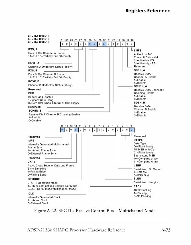
ADSP-2126x SHARC Processor Hardware Reference A-73
Registers Reference
Figure A-22. SPCTLx Receive Control Bits – Multichannel Mode
31 30 29 28 27 26 24 23 22 21 20 19 18 17 16
00 0 0 0 0 0 0 0 0 0 0 0 0 0 0
RXS_AData Buffer Channel A Status11=Full 10=Partially Full 00=Empty
LMFSActive Low MC Transmit Data valid1=Active low FS0=Active High FSROVF_A
Channel A Underflow Status (sticky) SDEN_AReceive DMA Channel A Enable1=Enable0=Disable
RXS_BData Buffer Channel B Status11=Full 10=Partially Full 00=Empty
ROVF_B
BHDBuffer Hang Disable1=Ignore Core Hang0=Core Stall when TXn full or RXn Empty
SCHEN_AReceive DMA Channel A Chaining Enable1=Enable0=DisableSDEN_BReceive DMA Channel B Enable1=Enable0=Disable
SCHEN_BReceive DMA Channel B Chaining Enable1=Enable0=Disable
Reserved
Channel B Underflow Status (sticky)
Reserved
Reserved
25
SPCTL1 (0xc01)SPCTL3 (0x401)SPCTL5 (0x801)
15 14 13 12 11 10 9 8 7 6 5 4 3 2 1 0
00 0 0 0 0 0 0 0 0 0 0 0 0 0 0
Reserved Reserved
IMFS DTYPEData Type00=Right Justify, Fill MSB with 0’s01=Right Justify, Sign extend MSB10=Compand µ-law11=Compand A-law
LSBFSerial Word Bit Order1=LSB First0=MSB FirstSLENSerial Word Length-1
PACK16/32 Packing1=Packing0=No Packing
Internally Generated Multichannel Frame Sync1=Internal Frame Sync0=External Frame Sync
OPMODESPORT Operation Mode1=I2S or Left-justified Sample pair Mode0=DSP Serial Mode/Multichannel Mode
CKREActive Clock Edge for Data and Frame Sync Sampling1=Rising Edge0=Falling Edge
Reserved
ICLKInternally Generated Clock1=Internal Clock0=External Clock

I/O Processor Registers
A-74 ADSP-2126x SHARC Processor Hardware Reference
Figure A-23. SPCTLx Transmit Control Bits – Multichannel Mode
31 30 29 28 27 26 24 23 22 21 20 19 18 17 16
00 0 0 0 0 0 0 0 0 0 0 0 0 0 0
TXS_AData Buffer Channel A Status11=Full 10=Partially Full 00=Empty
LTDVActive Low MC Transmit Data valid1=Active low FS0=Active High FS
TUVF_AChannel A Underflow Status (sticky)
SDEN_ASPORT Transmit DMA Channel A Enable1=Enable0=Disable
TXS_BData Buffer Channel B Status11=Full 10=Partially Full 00=EmptyTUVF_B
BHDBuffer Hang Disable1=Ignore Core Hang0=Core Stall when TXn Full or RXn Empty
SCHEN_ASPORT Transmit DMA Channel A Chaining Enable1=Enable0=DisableSDEN_BSPORT Transmit DMA Channel B Enable1=Enable0=Disable
SCHEN_BSPORT Transmit DMA Channel B Chaining Enable1=Enable0=Disable
Reserved
Channel B Underflow Status (sticky) Reserved
Reserved
25
SPCTL0 (0xc00)SPCTL2 (0x400)SPCTL4 (0x800)
15 14 13 12 11 10 9 8 7 6 5 4 3 2 1 0
00 0 0 0 0 0 0 0 0 0 0 0 0 0 0
Reserved Reserved
CKRE DTYPEData Type00=Right Justify, Fill MSB with 0’s01=Right Justify, Sign extend MSB10=Compand µ-law11=Compand A-lawLSBFSerial Word Bit Order1=LSB First0=MSB FirstSLENSerial Word Length-1
PACK16/32 Packing1=Packing0=No Packing
Active Clock Edge for Data and Frame Sync Driving1=Rising Edge0=Falling Edge
OPMODESPORT Operation Mode1=I2S or Left-justified Sample pair Mode0=DSP Serial Mode/Multichannel Mode
Reserved

ADSP-2126x SHARC Processor Hardware Reference A-75
Registers Reference
When changing SPORT operating modes, programs should clear a serial port’s control register before writing new settings to the control register.
Table A-23. SPCTLx Register Bit Descriptions
Bits Name Definition
0 SPEN_A Enable Channel A Serial Port. Enables if set, (= 1) or disables if cleared, (= 0) the corresponding serial port A channel.This bit is reserved when the SPORT is in Multichannel mode.
2–1 DTYPE Data Type Select. Selects the data type formatting for normal and mul-tichannel transmissions as follows:NormalMultiData Type Formatting00x0Right-justify, zero-fill unused MSBs 01x1Right-justify, sign-extend unused MSBs 100xCompand using μ-law 111xCompand using A-law
3 LSBF Serial Word Endian Select. Selects little-endian words (LSB first, if set, = 1) or big-endian words (MSB first, if cleared, = 0). This bit is reserved when the SPORT is in I²S or Left-Justified Sample Pair mode.
8–4 SLEN Serial Word Length Select. Selects the word length in bits. For DSP serial and multichannel modes, word sizes can be from 3 bits to 32 bits. For I²S and Left-justified modes, word sizes can be from 8 bits to 32 bits.
9 PACK 16-bit to 32-bit Word Packing Enable. Enables if set, (= 1) or disables if cleared, (= 0) 16- to 32-bit word packing.
10 ICLK Internal Clock Select. Selects the internal transmit clock if set, (= 1) or external transmit clock if cleared, (= 0). This bit applies to DSP Serial and multichannel modes.
MSTR (I2S mode only)
In I2S and Left-justified Sample Pair mode, this bit selects the word source and internal clock if set, (= 1) or external clock if cleared, (= 0)
11 OPMODE Sport Operation Mode. Selects the I2S/Left-justified Sample Pair mode if set (= 1) or DSP Serial/Multichannel mode if cleared (= 0).
12 CKRE Clock Rising Edge Select. Selects whether the serial port uses the rising edge if set, (= 1) or falling edge if cleared, (= 0) of the clock signal to sample data and the frame sync. CKRE is reserved when the SPORT is
in I2S and Left-justified Sample Pair mode.
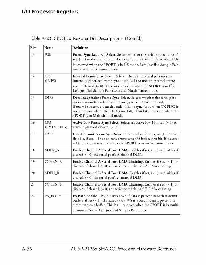
I/O Processor Registers
A-76 ADSP-2126x SHARC Processor Hardware Reference
13 FSR Frame Sync Required Select. Selects whether the serial port requires if set, (= 1) or does not require if cleared, (= 0) a transfer frame sync. FSR
is reserved when the SPORT is in I2S mode, Left-Justified Sample Pair mode and multichannel mode.
14 IFS(IMFS)
Internal Frame Sync Select. Selects whether the serial port uses an internally generated frame sync if set, (= 1) or uses an external frame
sync if cleared, (= 0). This bit is reserved when the SPORT is in I2S, Left-justified Sample Pair mode and Multichannel mode.
15 DIFS Data Independent Frame Sync Select. Selects whether the serial port uses a data-independent frame sync (sync at selected interval, if set, = 1) or uses a data-dependent frame sync (sync when TX FIFO is not empty or when RX FIFO is not full). This bit is reserved when the SPORT is in Multichannel mode.
16 LFS (LMFS, FRFS)
Active Low Frame Sync Select. Selects an active low FS if set, (= 1) or active high FS if cleared, (= 0).
17 LAFS Late Transmit Frame Sync Select. Selects a late frame sync (FS during first bit, if set, = 1) or an early frame sync (FS before first bit, if cleared, = 0). This bit is reserved when the SPORT is in multichannel mode.
18 SDEN_A Enable Channel A Serial Port DMA. Enables if set, (= 1) or disables if cleared, (= 0) the serial port’s A channel DMA.
19 SCHEN_A Enable Channel A Serial Port DMA Chaining. Enables if set, (= 1) or disables if cleared, (= 0) the serial port’s channel A DMA chaining.
20 SDEN_B Enable Channel B Serial Port DMA. Enables if set, (= 1) or disables if cleared, (= 0) the serial port’s channel B DMA.
21 SCHEN_B Enable Channel B Serial Port DMA Chaining. Enables if set, (= 1) or disables if cleared, (= 0) the serial port’s channel B DMA chaining.
22 FS_BOTH FS Both Enable. This bit issues WS if data is present in both transmit buffers, if set (= 1). If cleared (= 0), WS is issued if data is present in either transmit buffer. This bit is reserved when the SPORT is in multi-
channel, I2S and Left-justified Sample Pair mode.
Table A-23. SPCTLx Register Bit Descriptions (Cont’d)
Bits Name Definition

ADSP-2126x SHARC Processor Hardware Reference A-77
Registers Reference
SPORT Multichannel Control Registers (SPMCTLxy)
The SPORT Multichannel Control registers’ addresses are:
23 BHD Buffer Hang Disable. This bit ignores a core hang, when set (= 1). When cleared (= 0), this bit indicates a core stall. The core stall occurs when the transmit buffer is full or the receive buffer is empty and the core tries to write or read from the FIFO respectively. This bit applies to all modes
24 SPEN_B Enable Channel B Serial Port. Enables if set, (= 1) or disables if cleared, (= 0) the corresponding serial port B channel.This bit is reserved when the SPORT is in Multichannel mode.
25 SPTRAN Data Direction Control. Enables receive buffers if cleared (= 0), or acti-vates transmit buffers if set (= 1). This bit is reserved when the SPORT is in Multichannel mode.
26 ROVF_B, TUVF_B
Channel B Error Status (sticky, read-only). Indicates if the serial trans-mit operation has underflowed or a receive operation has overflowed in the channel B data buffer. This bit is reserved when the SPORT is in Multichannel mode.
28–27 DXS_B Channel B Data Buffer Status (read-only). Indicates the status of the serial port’s channel B data buffer as follows: 11 = full, 00 = empty, 10 = partially full. This bit is reserved when the SPORT is in Multichannel mode.
29 ROVF_A or TUVF_A
Channel A Error Status (sticky, read-only). Indicates if the serial trans-mit operation has underflowed or a receive operation has overflowed in the channel A data buffer.
31–30 RXS_A or TXS_A
Channel A Data Buffer Status (read-only). Indicates the status of the serial port’s channel A data buffer as follows: 11 = full, 00 = empty, 10 = partially full.
SPMCTL01 0xc04
SPMCTL23 0x404
SPMCTL45 0x804
Table A-23. SPCTLx Register Bit Descriptions (Cont’d)
Bits Name Definition

I/O Processor Registers
A-78 ADSP-2126x SHARC Processor Hardware Reference
The SPMCTL01 register is the Multichannel Control register for SPORTs 0 and 1. The SPMCTL23 register is the Multichannel Control register for SPORTs 2 and 3. The SPMCTL45 register is the Multichannel Control reg-ister for SPORTs 4 and 5. The reset value for these registers is undefined.
Figure A-24. SPMCTL01 Register – Multichannel Mode
31 30 29 28 27 26 24 23 22 21 20 19 18 17 16
00 0 0 0 0 0 0 0 0 0 0 0 0 0 0
DMACHS1B
SPORT1 Channel B StatusDMA Chaining Status
CHNL
Current Channel Status (read-only)
DMAS0A
SPORT0 Channel A StatusDMA Status
MCEB
Multichannel Enable, B Channels1=Enable0=Disable
DMACHS1A
SPORT1 Channel A StatusDMA Chaining Status
DMACHS0B
SPORT0 Channel B StatusDMA Chaining Status
DMACHS0A
SPORT0 Channel A StatusDMA Chaining Status
DMAS1B
SPORT1 Channel B Status/ DMA Status
DMAS1A
SPORT1 Channel A Status/DMA Status
DMAS0B
SPORT0 Channel B StatusDMA Status
15 14 13 12 11 10 8 7 6 5 4 3 2 1 0
00 0 0 0 0 0 0 0 0 0 0 0 0 0 0
ReservedSPL
MCEAMultichannel Enable, A Channels1=Enable0=Disable
MFDxMultichannel Frame Delay
SPORT LoopbackSPORT0 A to SPORT1 A OnlySPORT0 B to SPORT1 B Only
NCHNumber of Channels – 1
25
9
SPMCTL01 (0xc04)
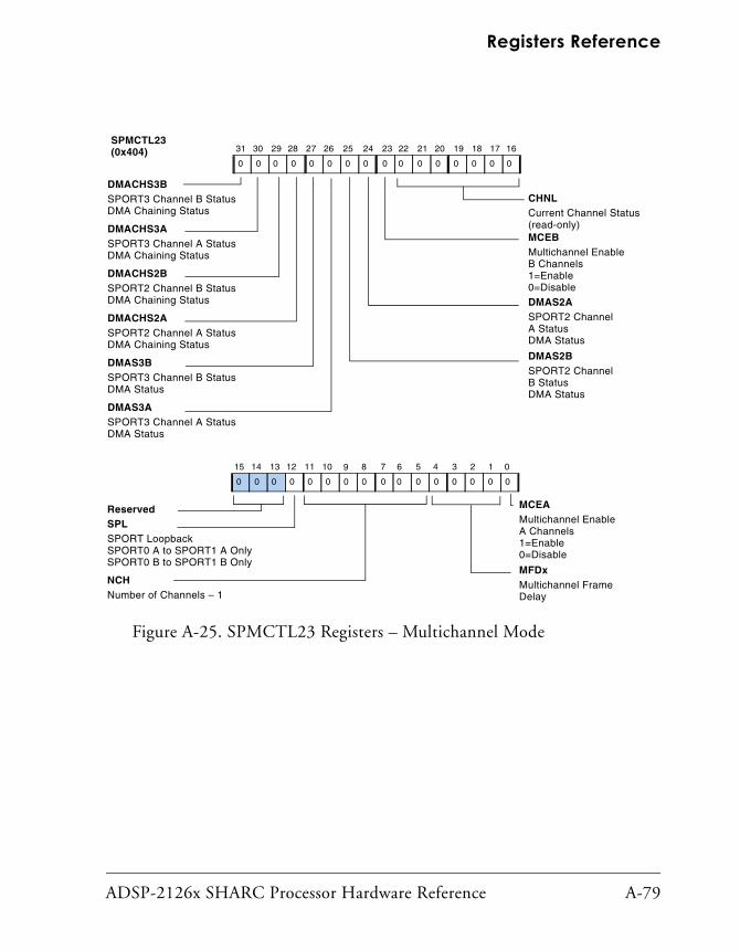
ADSP-2126x SHARC Processor Hardware Reference A-79
Registers Reference
Figure A-25. SPMCTL23 Registers – Multichannel Mode
31 30 29 28 27 26 24 23 22 21 20 19 18 17 16
00 0 0 0 0 0 0 0 0 0 0 0 0 0 0
DMACHS3BSPORT3 Channel B StatusDMA Chaining Status
CHNLCurrent Channel Status (read-only)
DMAS2ASPORT2 Channel A StatusDMA Status
MCEBMultichannel EnableB Channels1=Enable0=Disable
DMACHS3ASPORT3 Channel A StatusDMA Chaining Status
DMACHS2BSPORT2 Channel B StatusDMA Chaining Status
DMACHS2ASPORT2 Channel A StatusDMA Chaining Status
DMAS3BSPORT3 Channel B StatusDMA Status
DMAS3ASPORT3 Channel A StatusDMA Status
DMAS2BSPORT2 Channel B StatusDMA Status
15 14 13 12 11 10 8 7 6 5 4 3 2 1 0
00 0 0 0 0 0 0 0 0 0 0 0 0 0 0
ReservedSPL
MCEAMultichannel EnableA Channels1=Enable0=Disable
MFDxMultichannel Frame Delay
SPORT LoopbackSPORT0 A to SPORT1 A OnlySPORT0 B to SPORT1 B Only
NCHNumber of Channels – 1
25
9
SPMCTL23 (0x404)

I/O Processor Registers
A-80 ADSP-2126x SHARC Processor Hardware Reference
Figure A-26. SPMCTL45 Registers – Multichannel Mode
31 30 29 28 27 26 24 23 22 21 20 19 18 17 16
00 0 0 0 0 0 0 0 0 0 0 0 0 0 0
DMACHS5BSPORT3 Channel B StatusDMA Chaining Status
CHNLCurrent Channel Status (read-only)
DMAS4ASPORT2 Channel A StatusDMA Status
MCEBMultichannel EnableB Channels1=Enable0=Disable
DMACHS5ASPORT3 Channel A StatusDMA Chaining Status
DMACHS4BSPORT2 Channel B StatusDMA Chaining Status
DMACHS4ASPORT2 Channel A StatusDMA Chaining Status
DMAS5BSPORT3 Channel B StatusDMA Status
DMAS5ASPORT3 Channel A StatusDMA Status
DMAS4BSPORT2 Channel B Status DMA Status
15 14 13 12 11 10 8 7 6 5 4 3 2 1 0
00 0 0 0 0 0 0 0 0 0 0 0 0 0 0
ReservedSPL
MCEAMultichannel EnableA Channels1=Enable0=Disable
MFDxMultichannel Frame Delay
SPORT LoopbackSPORT3 A to C, B to D Only
NCHNumber of Channels – 1
9
25SPMCTL45 (0x804)
ADSP-2126x SHARC Processor Hardware Reference A-81
Registers Reference
For a detailed description of the bits in the SPMCTLxy register, refer to Table A-24.
Table A-24. SPMCTLxy Register Bit Descriptions
Bits Name Definition
0 MCEA Multichannel Mode Enable. Standard and Multichannel modes only. One of two configuration bits that enable and disable multi-channel mode on serial port channels. See also, OPMODE on page A-26.0 = Disable multichannel operation1 = Enable multichannel operation if OPMODE = 0
4–1 MFD Multichannel Frame Delay. Set the interval, in number of serial clock cycles, between the multichannel frame sync pulse and the first data bit. These bits provide support for different types of T1 interface devices. Valid values range from 0 to 15 with bits SPMCTL01 [4:1] or SPMCTL23[4:1] or SPMCTL45[4:1]. Val-ues of 1 to15 correspond to the number of intervening serial clock cycles. A value of 0 corresponds to no delay. The multichannel frame sync pulse is concurrent with first data bit.
11–5 NCH Number of Multichannel Slots (minus one). Select the number of channel slots (maximum of 128) to use for multichannel opera-tion. Valid values for actual number of channel slots range from 1 to 128. Use this formula to calculate the value for NCH: NCH = Actual number of channel slots – 1.

I/O Processor Registers
A-82 ADSP-2126x SHARC Processor Hardware Reference
12 SPL SPORT Loopback Mode. Enables if set (= 1) or disables if cleared (= 0) the channel loopback mode. Loopback mode enables devel-opers to run internal tests and to debug applications. Loopback only works under the following SPORT configurations:• SPORT0 (configured as a receiver or transmitter) together with
SPORT1 (configured as a transmitter or receiver). SPORT0 can only be paired with SPORT1, controlled via the SPL bit in the SPMCTL01 register.
• SPORT2 (as a receiver or transmitter) together with SPORT3 (as a transmitter or receiver). SPORT2 can only be paired with SPORT3, controlled via the SPL bit in the SPMCTL23 register.
• SPORT4 (configured as a receiver or transmitter) together with SPORT5 (configured as a transmitter or receiver). SPORT4 can only be paired with SPORT5, controlled via the SPL bit in the SPMCTL45 register. Either of the two paired SPORTs can be set up to transmit or receive, depending on their SPTRAN bit configurations.
15–13 Reserved
22–16 CHNL Current Channel Selected (Read-only, Sticky). Identify the cur-rently selected transmit channel slot (0 to 127).
23 MCEB Multichannel Enable, B Channels.0 = Disable1 = Enable
27–24 DMASxy DMA Status. Selects the transfer format.0 = Inactive 1 = Active(Read-only)
31–28 DMACHSxy DMA Chaining Status.0 = Inactive1 = Active)(Read-only)
Table A-24. SPMCTLxy Register Bit Descriptions (Cont’d)
Bits Name Definition

ADSP-2126x SHARC Processor Hardware Reference A-83
Registers Reference
SPORT Transmit Buffer Registers (TXSPx)
The addresses of the TXSPx registers are:
The reset value for these registers is undefined. The 32-bit TXSPx registers hold the output data for serial port transmit operations. For more infor-mation on how transmit buffers work, see “Transmit and Receive Data Buffers” on page 9-60.
SPORT Receive Buffer Registers (RXSPx)
The addresses of the RXSPx registers are:
The reset value for these registers is undefined. The 32-bit RXSPx registers hold the input data from serial port receive operations. For more informa-tion on how receive buffers work, see “Transmit and Receive Data Buffers” on page 9-60.
TXSP0A – 0xc60 TXSP0B – 0xc62
TXSP1A – 0xc64 TXSP1B – 0xc66
TXSP2A – 0x460 TXSP2B – 0x462
TXSP3A – 0x464 TXSP3B – 0x466
TXSP4A – 0x860 TXSP4B – 0x862
TXSP5A – 0x864 TXSP5B – 0x866
RXSP0A – 0xc61 RXSP0B – 0xc63
RXSP1A – 0xc65 RXSP1B – 0xc67
RXSP2A – 0x461 RXSP2B – 0x463
RXSP3A – 0x465 RXSP3B – 0x467
RXSP4A – 0x861 RXSP4B – 0x863
RXSP5A – 0x865 RXSP5B – 0x867

I/O Processor Registers
A-84 ADSP-2126x SHARC Processor Hardware Reference
SPORT Divisor Registers (DIVx)
The addresses of the DIVx registers are:
The reset value for these registers is undefined. These registers contain two fields:
• Bits 15–1 are CLKDIV. These bits identify the Serial Clock Divisor value for internally-generated SCLK as follows:
• Bits 31–16 are FSDIV. These bits select the Frame Sync Divisor for internally-generated TFS as follows:
DIV0 – 0xc02 DIV1 – 0xc03
DIV2 – 0x402 DIV3 – 0x403
DIV4 – 0x802 DIV5 – 0x803
Figure A-27. DIVx Register
CLKDIVfCCLK
4 fSCLK( )--------------------- 1–=
FSDIVfSCLK
fSFS------------ 1–=
31 30 29 28 27 26 24 23 22 21 20 19 18 17 16
00 0 0 0 0 0 0 0 0 1 0 0 0 0 0
FSDIV
15 14 13 12 11 10 8 7 6 5 4 3 2 1 0
00 0 0 0 0 0 0 0 0 1 0 0 0 0 0
CLKDIVClock Divisor
25
9
Frame Sync Divisor
Reserved

ADSP-2126x SHARC Processor Hardware Reference A-85
Registers Reference
SPORT Count Registers (SPCNTx)
The addresses of the SPCNTx registers are:
The reset value for these registers is undefined. The SPCNTx registers pro-vides status information for the internal clock and frame sync.
SPORT Transmit Select Registers (MTxCSy)
The addresses of the MTxCSy registers are:
The reset value for these registers is undefined.
Each bit, 31–0, set (= 1) in one of four MTxCSy registers corresponds to an active transmit channel, 127–0, on a Multichannel mode serial port. When the MTxCSy registers activate a channel, the serial port transmits the word in that channel’s position of the data stream. When a channel’s bit in the MTxCSy register is cleared (= 0), the serial port’s data transmit pin three-states during the channel’s transmit time slot.
SPCNT0 – 0xC15 SPCNT1 – 0xC16
SPCNT2 – 0x415 SPCNT3 – 0x416
SPCNT4 – 0x815 SPCNT5 – 0x816
MT0CS0 – 0xC05 MT0CS1 – 0xC06
MT0CS2 – 0xC07 MT0CS3 – 0xC08
MT2CS0 – 0x405 MT2CS1 – 0x406
MT2CS2 – 0x407 MT2CS3 – 0x408
MT4CS0 – 0x805 MT4CS1 – 0x806
MT4CS2 – 0x807 MT4CS3 – 0x808

I/O Processor Registers
A-86 ADSP-2126x SHARC Processor Hardware Reference
SPORT Transmit Compand Registers (MTxCCSy)
The addresses of the MTxCCSy registers are:
The reset value for these registers is undefined.
Each bit, 31–0, set (= 1) in one of four MTxCCSy registers corresponds to an companded transmit channel, 127–0, on a Multichannel mode serial port. When the MTxCCSy register activates companding for a channel, the serial port applies the companding from the serial port’s DTYPE selection to the transmitted word in that channel’s position of the data stream. When a channel’s bit in the MTxCCSy register is cleared (= 0), the serial port does not compand the output during the channel’s receive time slot.
SPORT Receive Select Registers (MRxCSy
The addresses of the MRxCSx registers are:
The reset value for these registers is undefined.
MT0CCS0 – 0xC0D MT0CCS1 – 0xC0E
MT0CCS2 – 0xC0F MT0CCS3 – 0xc10
MT2CCS0 – 0x40D MT2CCS1 – 0x40E
MT2CCS2 – 0x40F MT2CCS3 – 0x410
MT4CCS0 – 0x80D MT4CCS1 – 0x80E
MT4CCS2 – 0x80F MT4CCS3 – 0x810
MR1CS0 – 0xC09 MR1CS1 – 0xC0A
MR1CS2 – 0xC0B MR1CS3 – 0xC0C
MR3CS0 – 0x409 MR3CS1 – 0x40A
MR3CS2 – 0x40B MR3CS3 – 0x40C
MR5CS0 – 0x809 MR5CS1 – 0x80A
MR5CS2 – 0x80B MR5CS3 – 0x80C

ADSP-2126x SHARC Processor Hardware Reference A-87
Registers Reference
Each bit, 31–0, set (= 1) in one of the four MRCSx registers corresponds to an active receive channel, 127–0, on a Multichannel mode serial port. When the MRxCSx register activates a channel, the SPORT receives the word in that channel’s position of the data stream and loads the word into the RXSPx buffer. When a channel’s bit in the MRxCSx register is cleared (= 0), the serial port ignores any input during the channel’s receive time slot.
SPORT Receive Compand Registers (MRxCCSy)
These addresses for the MRxCCSy registers are:
The reset value for these registers is undefined.
Each bit, 31–0, set (= 1) in the MRxCCSy registers corresponds to an com-panded receive channel, 127–0, on a Multichannel mode serial port. When one of the four MRxCCSy registers activate companding for a chan-nel, the serial port applies the companding from the serial port’s DTYPE selection to the received word in that channel’s position of the data stream. When a channel’s bit in the MRxCCSy registers are cleared (= 0), the serial port does not compand the input during the channel’s receive time slot.
MR1CCS0 – 0xC11 MR1CCS1 – 0xC12
MR1CCS2 – 0xC13 MR1CCS3 – 0xC14
MR3CCS0 – 0x411 MR3CCS1 – 0x412
MR3CCS2 – 0x413 MR3CCS3 – 0x414
MR5CCS0 – 0x811 MR5CCS1 – 0x812
MR5CCS2 – 0x813 MR5CCS3 – 0x814

I/O Processor Registers
A-88 ADSP-2126x SHARC Processor Hardware Reference
SPORT DMA Index Registers (IISPx)
The addresses of the IISPx registers are:
The reset value for these registers is undefined. The IISPx register is 19 bits wide and it holds an address and acts as a pointer to memory for a DMA transfer. For more information, see “I/O Processor” in Chapter 7, I/O Processor.
SPORT DMA Modifier Registers (IMSPx)
The addresses of the IMSPx registers are:
The reset value for these registers is undefined. The IMSPx register is 16 bits wide and it provides the increment or step size by which an IISPx reg-ister is post-modified during a DMA operation. For more information, see “I/O Processor” in Chapter 7, I/O Processor.
IISP0A – 0xC40 IISP0B – 0xC44
IISP1A – 0xC48 IISP1B – 0xC4C
IISP2A – 0x440 IISP2B – 0x444
IISP3A – 0x448 IISP3B – 0x44C
IISP4A – 0x840 IISP4B – 0x844
IISP5A – 0x848 IISP5B – 0x84C
IMSP0A – 0xC41 IMSP0B – 0xC45
IMSP1A – 0xC49 IMSP1B – 0xC4D
IMSP2A – 0x441 IMSP2B – 0x445
IMSP3A – 0x449 IMSP3B – 0x44D
IMSP4A – 0x841 IMSP4B – 0x845
IMSP5A – 0x849 IMSP5B – 0x84D
ADSP-2126x SHARC Processor Hardware Reference A-89
Registers Reference
SPORT DMA Count Registers (CSPx)
The CSPx registers’ addresses are:
The reset value for these registers is undefined. The CSPx registers are 16 bits wide and they hold the word count for a DMA transfer. For more information, see “I/O Processor” in Chapter 7, I/O Processor.
SPORT Chain Pointer Registers (CPSPxx)
The addresses of the CPSPxx registers are:
The reset value for these registers is undefined. The CPSPxx registers are 20 bits wide and they hold the address for the next Transfer Control Block in a chained DMA operation. For more information, see “I/O Processor” in Chapter 7, I/O Processor.
CSP0A – 0xC42 CSP0B – 0xC46
CSP1A – 0xC4A CSP1B – 0xC4E
CSP2A – 0x442 CSP2B – 0x446
CSP3A – 0x44A CSP3B – 0x44E
CSP4A – 0x842 CSP4B – 0x846
CSP5A – 0x84A CSP5B – 0x84E
CPSP0A – 0xC43 CPSP0B – 0xC47
CPSP1A – 0xC4B CPSP1B – 0xC4F
CPSP2A – 0x443 CPSP2B – 0x447
CPSP3A – 0x44B CPSP3B – 0x44F
CPSP4A – 0x843 CPSP4B – 0x847
CPSP5A – 0x84B CPSP5B – 0x84F
I/O Processor Registers
A-90 ADSP-2126x SHARC Processor Hardware Reference
SPI RegistersThe following sections describe the registers associated with the Serial Peripheral Interface (SPI).
SPI Port Status Register (SPISTAT)
The SPI Status register (SPISTAT) is used to detect when an SPI transfer is complete or if transmission/reception errors occur. The SPISTAT register can be read at any time.
Some of the bits in the SPISTAT register are read-only (RO) and cannot be cleared. The remainder of the bits can be read, but can also be cleared by a write one-to-clear (W1C-type) operation. Bits that provide information about the SPI are also read-only; these bits get set and cleared by the hard-ware. Bits that are W1C-type are set when an error condition occurs (see Table A-25 on page A-91); these bits are set by hardware and must be cleared by software. To clear a W1C-type bit, the program must write a one to the desired bit position of the SPISTAT register. For example, if the TUNF bit is set, the program must write a one to bit 2 of SPISTAT to clear the TUNF error condition. This allows the program to read the status register without changing its value.
Write one-to-clear (W1C-type) bits can only be cleared by writing 1 to them. Writing zero does not clear (or have any effect on) a W1C-type bit. Table A-25 provides the bit descriptions for the SPISTAT register.

ADSP-2126x SHARC Processor Hardware Reference A-91
Registers Reference
Figure A-28. SPISTAT Register
Table A-25. SPISTAT Register Bits
Bit Name Function Type Default
0 SPIF SPIRCV bits in SPICTL. Set to 1 when the appropriate shift-register has completed shift-ing in or out data.
RO 1
1 MME Multimaster Error or Mode-fault Error. Set when the processor is configured as the SPI master and another device tries to become the master by driving the SPIDS signal low. See “Mode Fault Error (MME)” on page 10-40.
W1C 0
2 TUNF Transmission Error (Underflow). Set when a transmission occurred with no new data in the TXSPI register. See “Transmission Error Bit (TUNF)” on page 10-41.
W1C 0
31 30 29 28 27 26 24 23 22 21 20 19 18 17 16
00 0 0 0 0 0 0 0 0 0 0 0 0 0 0
Reserved
15 14 13 12 11 10 8 7 6 5 4 3 2 1 0
00 0 0 0 0 0 0 0 0 0 0 0 0 0 0
ReservedTXCOL
SPIFSPI Transmit Transfer Complete1=Transfer Complete0=Transfer Active
MMEMultimaster Error1=SPIDS Asserted by Slave0=No Error
Transmit Collision Error
RXS
Data Buffer Status (read-only)1=Full0=Empty
ROVFReception Error (Overflow)1=New Data Received with Full RXSPI Buffer TUNF
Transmission Error (Under-flow)1=No New Data in TXSPI Buffer
TXS
Data Buffer Status (read-only)1=Full0=Empty
25
9
SPISTAT (0x1002)

I/O Processor Registers
A-92 ADSP-2126x SHARC Processor Hardware Reference
The transmit buffer is full after data is written to it and is empty when a transfer begins and the transmit value loads into the Shift register. The receive buffer is full at the end of a transfer when the Shift register value is loaded into the receive buffer. It is empty when the receive buffer is read.
The SPI status also depends on the PACKEN bit in the SPICTL register. If packing is enabled, then the receive buffer status is set to full only after two transfers from the Shift register.
3 TXS Transmit Data Buffer Status. Indicates the TXSPI data buffer status.0 = Empty1 = Full
RO 0
4 ROVF Reception Error (Overflow). Set when data is received and the receive buffer is full.1 = New data received with full RXSPI regis-ter. See “Reception Error Bit (ROVF)” on page 10-42.
W1C 0
5 RXS Receive Data Buffer Status. Indicates the RXSPI data buffer status.0 = Empty1 = Full
RO 0
6 TXCOL Transmission Collision Error. The TXCOL flag is set in the SPISTAT register when a write to the TXSPI register coincides with the load of the shift register. See “Transmit Colli-sion Error Bit (TXCOL)” on page 10-42
W1C 0
31–7 Reserved
Table A-25. SPISTAT Register Bits (Cont’d)
Bit Name Function Type Default

ADSP-2126x SHARC Processor Hardware Reference A-93
Registers Reference
SPI Port Flags Register (SPIFLG)
This register’s address is 0x1001. The reset value for this register is 0x0F80.The SPIFLG register is used to enable individual SPI slave select lines when the SPI is enabled as a master.
Figure A-29. SPIFLG Register
Table A-26. SPIFLG Register Bits
Bit Name Function
3–0 DSxEN(3–0)
SPI Device Select Bits. This bit enables or disables if set, (= 1 or if cleared = 0) the corresponding flag output to be used for an SPI slave-select.
6–4 Reserved
7 ISSS Input Service Select Bit. This read-only bit reflects the status of the slave select input pin.
11–8 SPIFLGx(3–0)
SPI Device Select Control. This bit if cleared, (= 0) selects a corre-sponding flag output to be used for SPI slave-select.
31–12 Reserved
31 30 29 28 27 26 24 23 22 21 20 19 18 17 16
00 0 0 0 0 0 0 0 0 0 0 0 0 0 0
Reserved
15 14 13 12 11 10 8 7 6 5 4 3 2 1 0
00 0 0 0 1 1 1 1 0 0 0 0 0 0 0
ReservedSPIDSx
DSxENSPI Device Select Enable1=Enable0=DisableReserved
SPI Device Select Control1=Disable0=EnableISSSStatus of Input Slave Select Pin
24
9
SPIFLG (0x1001)

I/O Processor Registers
A-94 ADSP-2126x SHARC Processor Hardware Reference
SPI Control Register (SPICTL)
This register’s address is 0x1000. The reset value for this register is 0x0400. The SPI Control register (SPICTL) is used to configure and enable the SPI system. This register is used to set up SPI configurations such as selecting the device as a master or slave or determining the data transfer rate and word size.
Figure A-30. SPICTL Register (Upper bits)
31 30 29 28 27 26 24 23 22 21 20 19 18 17 16
00 0 0 0 0 0 0 0 0 0 0 0 0 0 0
ReservedSGN
Sign-extend Data1=Sign-extend0=No Sign-extend
SMLS
Seamless Transfer1=Enable0=Disable
TXFLSH
Transmit Buffer Flush1=SPITX Cleared0=SPITX Not Cleared
RXFLSH
Receive Buffer Flush1=SPIRX Cleared0=SPIRX Not Cleared
25SPICTL (0x1000) (Bits 31–16)

ADSP-2126x SHARC Processor Hardware Reference A-95
Registers Reference
Figure A-31. SPICTL Register (Lower bits)
15 14 13 12 11 10 8 7 6 5 4 3 2 1 0
00 0 0 0 0 0 0 0 0 0 0 0 0 0 0
PACKENTIMODTransfer Initiation Mode00=Initiate Transfer by Read of Receive Buffer01=Initiate Transfer by Write of Transmit Buffer10=Enable DMA Transfer Mode11=Reserved
Reserved
8-Bit Packing Enable1=8 to 16-bit Packing0=No Packing
SPIEN
SPI System Enable1=Enable0=Disable
OPDOpen Drain Output Enable for Data Pins1=Open Drain0=Normal
SPIMSMaster Slave Mode Bit1=SPI Master Device0=SPI Slave Device
CLKPLClock Polarity1=Active-Low SPICLK, High in Idle State0=Active-High SPICLK, Low in Idle State
CPHASE
Clock Phase1=SPICLK Toggles at Start of 1st Data Bit0=SPICLK Toggles at Middle of 1st Data Bit
MSBF
Most Significant Byte First1=MSB Sent/Received First0=LSB Sent/Received First
SENDZ
Send Zero/Repeat Byte when SPITX Empty1=Repeat Last Data0=Send Zero
GM
Fetch/Discard Incoming Data when SPIRX Full1=Overwrite with New Data0=Discard Incoming Data
ISSEN
Input Slave Select Enable1=Enable0=Disable
DMISO
Disable MISO Pin (Broad-cast)1=MISO Disabled0=MISO Enabled
WL
Word Length00=8 bits, 01=16 bits, 10=32 bits, 11=Reserved
9SPICTL (0x1000) (Bits 15–0)

I/O Processor Registers
A-96 ADSP-2126x SHARC Processor Hardware Reference
Table A-27. SPICTL Register Bit Descriptions
Bits Name Definition
1–0 TIMOD Transfer Initiation Mode. Defines the transfer initiation mode and interrupt generation. 00 = Initiate transfer by read of receive buffer. Interrupt active when receive buffer is full.01 = Initiate transfer by write to transmit buffer. Interrupt active when transmit buffer is empty.10 = Enable DMA Transfer mode. Interrupt configured by DMA11 = Reserved
2 SENDZ Send Zero. Send Zero or last word when TXSPI is empty.0 = Send Last Word1 = Send Zeros
3 GM Get Data. When RXSPI is full, get data or discard incoming data.0 = Discard incoming data 1 = Get more data, overwrites the previous data
4 ISSEN Input Slave Select Enable. Enables Slave-Select (SPIDS) input for the master. When not used, SPIDS can be disabled, freeing up a chip pin as a general-purpose I/O pin. 0 = Disable1 = Enable
5 DMISO Disable MISO Pin. Disables MISO as an output in an environ-ment where the master wishes to transmit to various slaves at one time (broadcast). Only one slave is allowed to transmit data back to the master. Except for the slave from whom the master wishes to receive, all other slaves should have this bit set.0 = MISO Enabled1 = MISO Disabled
6 Reserved
8–7 WL Word Length. 00 = 8 bits, 01 = 16 bits, 10 = 32 bits
9 MSBF Most Significant Byte First.1 = MSB sent/received first0 = LSB sent/received first
10 CPHASE Clock Phase. Selects the transfer format.0 = SPICLK starts toggling at the middle of 1st data bit1 = SPICLK starts toggling at the start of 1st data bit

ADSP-2126x SHARC Processor Hardware Reference A-97
Registers Reference
11 CLKPL Clock Polarity.0 = Active-high SPICLK (SPICLK low is the idle state)1 = Active-low SPICLK (SPICLK high is the idle state)
12 SPIMS Master Select. Configures SPI module as master or slave0 = Device is a slave device1 = Device is a master device
13 OPD Open Drain Output Enable. Enables open drain data output enable (for MOSI and MISO) 0 = Normal 1 = Open Drain
14 SPIEN SPI Port Enable. 0 = SPI Module is disabled1 = SPI Module is enabled
15 PACKEN Packing Enable.0 = No Packing1 = 8-16 PackingNote: This bit may be 1 only when WL = 00 (8-bit transfer). When in transmit mode, PACKEN bit will unpack data.
16 SGN Sign Extend Bit.0 = No sign extension1 = Sign Extension
17 SMLS Seamless Transfer Bit.0 = Seamless transfer disabled1 = Seamless transfer enabled not supported in modeTIMOD[1:0] = 00 and CPHASE = 0 for all modes.
18 TXFLSH Flush Transmit Buffer. Write a 1 to this bit to clear TXSPI0 = TXSPI not Cleared1 = TXSPI Cleared
19 RXFLSH Clear RXSPI. Write a 1 to this bit to clear RXSPI0 = RXSPI not Cleared1 = RXSPI Cleared
31–20 Reserved
Table A-27. SPICTL Register Bit Descriptions (Cont’d)
Bits Name Definition

I/O Processor Registers
A-98 ADSP-2126x SHARC Processor Hardware Reference
Shift Registers
The processor core contains two separate 32-bit shift registers—one for reception (RXSR) and one for transmission (TXSR).
Receive Shift Register (RXSR)
The RXSR register is clocked on the sampling edge of the SPICLK clock. The active edge is the opposite edge from the sampling edge. The RXSR register behaves the same way whether the device is in Slave or Master mode.
The register is configured by the MSBF and WL bits of the SPICTL register. The MSBF bit indicates the data format (LSB-first or MSB-first) and selects the direction of the shift. The WL bit indicates the length of the transfer—8 bits if WL = 00, 16 bits if WL = 01, and 32 bits if WL = 10. For more infor-mation, see “SPI Control Register (SPICTL)” on page A-94.
Transmit Shift Register (TXSR)
The TXSR register is clocked on the active or shifting edge. The active edge is the opposite edge from the sampling edge. The TXSR register can be shifted right or left, depending on the direction of the data flow. This reg-ister can also be loaded from the TXSPI register with data that is to be transmitted.
This register behaves the same way whether the device is in Slave or Mas-ter mode. The TXSR register contains 32 shift cells.
Each Shift register is configured by the MSBF and WL bits of the SPICTL reg-ister. The MSBF bit indicates the data format (LSB-first or MSB-first) and selects the direction of the shift. The WL bit indicates the length of the transfer—8 bits if WL = 00, 16 bits if WL = 01, and 32 bits if WL = 10. When WL = 00, the upper 24 MSBs of the register loads with zeroes after a write to the TXSPI register. For more information, see “SPI Control Register (SPICTL)” on page A-94.

ADSP-2126x SHARC Processor Hardware Reference A-99
Registers Reference
SPI Receive Data Buffer Shadow Register (RXSPI_SHADOW)
Use the RXSPI_SHADOW register for the receive data buffer (RXSPI) to debug software. The RXSPI_SHADOW register resides at a different address from RXSPI, but its contents are identical to the RXSPI. When RXSPI is read via the software, the RXS bit clears and an SPI transfer may be initiated (if TIMOD = 00). No such hardware action occurs when the shadow register is read. The RXSPI_SHADOW register is a read-only (RO) register accessible only by the software and not the DMA. For more information, see “SPI Receive Buffer Register (RXSPI)” on page A-98.
SPI Receive Buffer Register (RXSPI)
The SPI Receive Buffer register’s address is 0x1004. The reset value for this register is undefined. This is a 32-bit read-only register accessible by the core or DMA controller. At the end of a data transfer, the RXSPI regis-ter is loaded with the data in the Shift register. During a DMA receive operation, the data in RXSPI is automatically loaded into the internal memory. For core- or interrupt-driven transfers, programs can also use the RXS status bits in the SPISTAT register to determine if the receive buffer is full.
SPI Transmit Data Buffer Register (TXSPI)
The SPI Transmit Buffer register’s address is 0x1003.The reset value for this register is undefined. This SPI Transmit Data register is a 32-bit reg-ister which is part of the IOP register set and can be accessed by the core or the DMA controller. Data is loaded into this register before being transmitted. Prior to the beginning of a data transfer, data in the TXSPI register is automatically loaded into the Transmit Shift register. During a DMA transmit operation, the data in the TXSPI register is automatically loaded from internal memory.

I/O Processor Registers
A-100 ADSP-2126x SHARC Processor Hardware Reference
SPI Baud Rate Register (SPIBAUD)
The SPI Baud Rate register’s address is 0x1005 and its reset value is unde-fined. This SPI register is a 16-bit read-write register that is used to set the bit transfer rate for a master device. When configured as a slave, the value written to this register is ignored. The SPIBAUD register can be read or written at any time.
Writing a value of zero or one to the register disables the serial clock. Therefore, the maximum serial clock rate is one-fourth the core clock rate (CCLK).
Table A-28. SPIBAUD Register Bit Descriptions
Bits Name Definition
0 Reserved
15–1 BAUDR Enables the SPICLK per the following equation:SPICLK baud rate = core clock (CCLK)/4 x BAUDR)Default = 0.
31–16 Reserved
Table A-29. SPI Master Baud Rate Example
BAUDR(Decimal Value)
SPI Clock Divide Factor Baud Rate for CCLK @ 200 MHz
0 N/A N/A
1 4 50.0 MHz
2 8 25.0 MHz
3 12 16.67 MHz
4 16 12.5 MHz
32,767, (0x7FFF) 131,068 1.53 KHz

ADSP-2126x SHARC Processor Hardware Reference A-101
Registers Reference
SPI DMA RegistersThere are five SPI DMA-specific registers which are described in the fol-lowing sections.
SPI DMA Configuration (SPIDMAC) Register
The SPI DMA Configuration Register contains the control bits for SPI DMA transfers. Table A-30 provides the bit descriptions for the SPIDMAC register.
The SPIMME, SPIUNF, and SPIOVF bits are sticky; these bits remain set even if the corresponding SPISTAT bits (MME, TUNF, and ROVF) are cleared. To clear these bits, clear corresponding bits in the SPISTAT, register then con-figure a new DMA

I/O Processor Registers
A-102 ADSP-2126x SHARC Processor Hardware Reference
Figure A-32. SPIDMAC Register
31 30 29 28 27 26 25 24 23 22 21 20 19 18 17 16
00 0 0 0 0 0 0 0 0 0 0 0 0 0 0
SPICHSReserved
15 14 13 12 11 10 9 8 7 6 5 4 3 2 1 0
00 0 0 0 0 0 0 0 0 0 0 0 0 0 0
SPIDENSPIDMAS
DMA Transfer Status1=DMA Transfer in Progress0=DMA Idle
DMA Chain Loading Status1=DMA Chain Pointer Loading in Progress0=DMA Chain Idle
SPIERRSDMA Error Status1=Error During Transfer0=Successful DMA Transfer
SPISxDMA FIFO Status00=FIFO Empty 11=FIFO Full 10=FIFO Partially Full
DMA Enable1=DMA Enable0=DMA Disable
SPIRCV
DMA Write/Read1=SPI DMA Read0=SPI DMA Transmit
SPIMMEMultimaster Error1=Error During Transfer0=Successful Transfer
SPIUNFTransmit Underflow Error (DMADIR=0)1=Transmission Error Occurred with DMA FIFO Empty0=Successful Transfer
Receive Overflow Error (DMADIR=1)1=Error-Data Received with DMA FIFO Full0=Successful Transfer
SPIOVF
INTEN
Enable DMA Interrupt on Transfer1=Enable0=Disable
Reserved
DMA FIFO Clear1=Enable0=Disable
FIFOFLSH
Enable Interrupt on Error1=Enable0=Disable
INTERR
SPI DMA Chaining Enable1=Enable0=Disable
SPICHEN
Reserved
SPIDMAC (0x1084)

ADSP-2126x SHARC Processor Hardware Reference A-103
Registers Reference
Table A-30. SPIDMAC Register Bits
Bit(s) Name Function Type Default
0 SPIDEN DMA Enable. Enables if set (= 1) or dis-ables if cleared (= 0) DMA for the SPI port.
Control 0
1 SPIRCV DMA Direction. When set, the IOP emp-ties the RXSPI buffer, when cleared, the IOP fills the TXSPI buffer.0 = SPI Transmit DMA (Memory read)1 = SPI Receive DMA (Memory write)
Control 0
2 INTEN Enable DMA Interrupt. Enables if set (= 1) or disables if cleared (= 0) an inter-rupt upon completion of the DMA trans-fer.
Control 0
3 Reserved
4 SPICHEN SPI DMA Chaining Enable. Enables if set (=1) or disables if cleared (= 0) DMA chaining.
Control 0
6:5 Reserved
7 FIFOFLSH DMA FIFO Flush. Clears the four-deep FIFO and FIFO status bits if set (= 1). Once a one is written to this bit, it remains set. A zero need to be written to clear this bit.
Control 0
8 INTERR Enable Interrupt on Error. Enables if set (= 1) or disables if cleared (= 0) an inter-rupt when an error in the transmission occurs.
Control 0
9 SPIOVF Receive Overflow Error (SPIRCV=1). Set when SPIRCV = 1 and data is received with the receive buffer full (1 = error data received with receive data buffer RXSPI full in receive mode DMA).
Status 0
10 SPIUNF SPI Transmit Underrun Error. Set when SPIRCV = 0 and the SPI transmits without any new data in the transmit buffer TXSPI.
Status 0

I/O Processor Registers
A-104 ADSP-2126x SHARC Processor Hardware Reference
SPI DMA Start Address Register (IISPI)
The SPI DMA Start Address (IISPI) register’s address is 0x1080. The reset value for this register is undefined. This SPI register is a 19-bit read/write register that contains the start address of the buffer in memory.
SPI DMA Address Modifier Register (IMSPI)
The SPI DMA Address Modifier (IMSPI) register’s address is 0x1081. The reset value for this register is undefined. This SPI register is a 16-bit read/write register that contains the address modifier.
11 SPIMME SPI Multimaster Error. Set when MME is set in the SPISTAT register and DMA is enabled.
Status 0
13:12 SPISx DMA FIFO Status 0. Indicates the status of the DMA FIFO as follows:00 = FIFO empty11 = FIFO full10 = FIFO partially full01 = Reserved
Status
14 SPIERRS DMA Error Status. Set if any of the fol-lowing error bits get set: SPIOVF, SPIUNF, or SPIMME
Status 0
15 SPIDMAS DMA Transfer Status. Indicates the status of the DMA transfer as follows:1 = DMA in progress, 0 = DMA idle
Status 0
16 SPICHS DMA Chain Loading Status. Indicates the status of the DMA chain loading as fol-lows: 1 = DMA chain pointer loading in prog-ress, 0 = Chain idle
Status 0
31:17 Reserved
Table A-30. SPIDMAC Register Bits (Cont’d)
Bit(s) Name Function Type Default

ADSP-2126x SHARC Processor Hardware Reference A-105
Registers Reference
SPI DMA Word Count Register (CSPI)
This 16-bit register contains the number of DMA words to be transferred. When this register decrements from one to zero, the DMA is complete, and an interrupt may be triggered.
To prematurely end a DMA transfer, software should write the value one to the Count register so that it will decrement to zero. Writing a value of zero causes the count to decrement to a negative number, and this is not advised.
SPI DMA Chain Pointer Register (CPSPI)
This register contains the address of the Transfer Control Block (TCB) in memory when DMA chaining is enabled. This register’s address is 0x1083 and its reset value is undefined. For more information, see “Transfer Con-trol Block Chain Loading (TCB)” on page 7-13.
Table A-31 provides the bit descriptions for the CPSPI register.
Parallel Port RegistersThe Parallel Port peripheral in the ADSP-2126x processor includes several user-accessible registers. One register, (PPCTL), contains control and status. Two registers, (RXPP and TXPP), are used for buffering receive and transmit
Table A-31. CPSPI Register Bits
Bits Function Default
18:0 Next Chain Pointer Address. The address of the next transfer control block (TCB) in memory.
0
19 PCI – Program Controlled Interrupt. Affects interrupt functionality when DMA chaining is enabled. Setting this bit (= 1) causes an inter-rupt to occur after each DMA in the chain completes. Clearing this bit (= 0) causes an interrupt to occur only after the final DMA transfer in the chain is completed.
0

I/O Processor Registers
A-106 ADSP-2126x SHARC Processor Hardware Reference
operations. Six registers are used for DMA functionality—IIPP, IMPP, ICPP, EIPP, EMPP, and ECPP.
Table A-32. Parallel Port Registers
Function Registers Description
Control and Status Register
PPCTL “Parallel Port Control Register (PPCTL)” on page A-107
Buffering Receive and Transmit Data
TXPP “Parallel Port DMA Transmit Register (TXPP)” on page A-109
RXPP “Parallel Port DMA Receive Register (RXPP)” on page A-110
DMA functionality IIPP “Parallel Port DMA Start Internal Index Address Register (IIPP)” on page A-110r
IMPP “Parallel Port DMA Internal Modifier Address Reg-ister (IMPP)” on page A-110
ICPP “Parallel Port DMA Internal Word Count Register (ICPP)” on page A-110
EIPP “Parallel Port DMA Start External Index Address Register (EIPP)” on page A-110
EMPP “Parallel Port DMA External Modifier Address Reg-ister (EMPP)” on page A-111
ECPP “Parallel Port DMA External Word Count Register (ECPP)” on page A-111

ADSP-2126x SHARC Processor Hardware Reference A-107
Registers Reference
Parallel Port Control Register (PPCTL)
The Parallel Port Control Register (PPCTL) is used to configure and enable the parallel port system. This register’s address is 0x1800. Figure A-33 and Table A-33 describe the bits in this register.
Figure A-33. PPCTL Register
31 30 29 28 27 26 25 24 23 22 21 20 19 18 17 16
00 0 0 0 0 0 0 0 0 0 0 0 0 0 0
PPDSReserved
15 14 13 12 11 10 9 8 7 6 5 4 3 2 1 0
00 0 0 0 0 0 0 0 0 1 1 0 1 1 1
PPEN
PPALEPLParallel Port ALE Polarity1=ALE is Active Low0=ALE is Active High
Internal DMA Status1=If Internal Interface is Busy
PPBHDBus Hang Disable1=Disable Bus Hang0=Enable Bus HangPPSFIFO Status00=RXPP/TXPP Empty01=RXPP/TXPP Partially Full11=RXPP/TXPP Full
Parallel Port System Enable1=Enabled0=Disabled
PPDURParallel Port Data Cycle Duration00000; 00001=Reserved00010=3 clock cycles; 66 MHz 00011=4 clock cycles; 50 MHz 00100=5 clock cycles; 40 MHz 00101=6 clock cycles; 33 MHz...11111=32 clock cycles; 6.25 MHz
PPTRANExternal Memory Read/Write1=Write to External Memory0=Read from External Memory
PPBHC
External Data Width1=16-bit Width0=8-bit Width
Bus Hold Cycle1=Bus Hold Cycle at End of Every Access0=No Bus Hold Cycle
PP16
PPBS
Bus Status1=If External Interface is Busy
Reserved
PPDENDMA Enable1=Enable DMA0=Disable DMA
PPCTL (0x1800)

I/O Processor Registers
A-108 ADSP-2126x SHARC Processor Hardware Reference
Table A-33. Parallel Port Register (PPCTL) Bit Definitions
Bit Name Definition Default
0 PPEN Parallel Port Enable. Enables if set, (= 1) or disables if cleared, (= 0) the parallel port. Clearing this bit clears FIFO and status. If an RD, WR, or ALE cycle has already started, it completes normally before the port is disabled. The parallel port is ready to transmit or receive 2 cycles after enabling. An ALE cycle always occurs before the first read or write cycle after PPEN is enabled.
0
5–1 PPDUR Parallel Port Duration. The duration of Parallel Port data cycles is based on core-clock and controlled by these five bits as follows:00000 = Reserved00001 = Reserved00010 = 2 Wait States = 3 Core Clock Cycles; 66 MHz throughput00011 = 3 Wait States = 4 Core Clock Cycles; 50 MHz throughput00100 = 4 Wait States = 5 Core Clock Cycles; 40 MHz throughput00101 = 5 Wait States = 6 Core Clock Cycles; 33 MHz throughput... 11111 = 31 wait states; 6.25MHz throughput
Bit 1 = 1Bit 2=1Bit 3=1Bit 4=0Bit 5=1
6 PPBHC Bus Hold Cycle. Inserts a bus hold cycle at the end of every access (read or write cycle) if set, (= 1) or no bus hold cycle occurs if cleared, (= 0). During a BHC address and/or data continue to be driven for one cycle.
1
7 PP16 Parallel Port External Data Width. Selects the external data width to 16 bits if set, (= 1) or 8 bits if cleared, (= 0).
0
8 PPDEN Parallel Port DMA Enable. Enables if set, (= 1) DMA on the parallel port or disables DMA if cleared, (= 0). When PPDEN is cleared, any DMA requests already in the pipe-line complete, and no new DMA requests are made. This does not affect FIFO status.
0
9 PPTRAN Parallel Port Transmit/Receive Select. Indicates if the processor is reading from external memory if cleared, (= 0) or writing to external memory if set, (= 1).
0

ADSP-2126x SHARC Processor Hardware Reference A-109
Registers Reference
Parallel Port DMA Transmit Register (TXPP)
This register’s address is 0x1808. This Transmit Data register is a 32-bit register that is part of the IOP register set and can be accessed by the core or the DMA controller. Data is loaded into this register before being transmitted. Prior to the beginning of a data transfer, data in the TXPP reg-ister is automatically loaded into the Transmit Shift register. During a DMA transmit operation, the data in TXPP is automatically loaded from internal memory.
11-10 PPS Parallel Port FIFO Status. These read-only bits indicate the status of the parallel port FIFO as follows: 00 = RXPP/TXPP is empty01 = RXPP/TXPP is partially full11 = RXPP/TXPP is full
0
12 PPBHD Parallel Port Buffer Hang Disable. When cleared (= 0), core stalls occur normally when the core attempts to write to a full transmit buffer or read from an empty receive buf-fer. Prevents a core hang when set (= 1). The old data pres-ent in the receive buffer is read again if the core tries to read it. If a write to the transmit buffer is performed, the core will overwrite the current data in the buffer.
0
13 PPALEPL Parallel Port ALE Polarity Level. Asserts ALE active low if set, (= 1) or active high if cleared, (= 0).
0
15–14 Reserved 0
16 PPDS DMA Status. Indicates that the internal DMA interface is active if set, (= 1) or not active if cleared, (= 0).
0
17 PPBS Parallel Port Bus Status. Indicates that the external bus interface is busy if set, (= 1) or available if cleared, (= 0). The bus will be “busy” until one ALE cycle, RD cycle or WR cycle has taken place.
0
31–18 Reserved 0
Table A-33. Parallel Port Register (PPCTL) Bit Definitions (Cont’d)
Bit Name Definition Default

I/O Processor Registers
A-110 ADSP-2126x SHARC Processor Hardware Reference
Parallel Port DMA Receive Register (RXPP)
This register’s address is 0x1809. This is a 32-bit read-only register acces-sible by the core or the DMA controller. At the end of a data transfer, RXPP is loaded with the data in the shift register. During a DMA receive operation, the data in the RXPP register is automatically loaded into the internal memory. For core or interrupt driven transfer, you can also use the RXS status bits in the PPSTAT register to determine if the receive buffer is full.
Parallel Port DMA Start Internal Index Address Register (IIPP)
This register’s address is 0x1818. This 19-bit register contains the offset from the DMA starting address of 32-bit internal memory.
Parallel Port DMA Internal Modifier Address Register (IMPP)
This register’s address is 0x1819. This 16-bit register contains the internal memory DMA address modifier.
Parallel Port DMA Internal Word Count Register (ICPP)
This register’s address is 0x181A. This 16-bit register contains the number of words in internal memory to be transferred via DMA.
Parallel Port DMA Start External Index Address Register (EIPP)
This register’s address is 0x1810. This 24-bit register contains the external memory DMA address index.

ADSP-2126x SHARC Processor Hardware Reference A-111
Registers Reference
Parallel Port DMA External Modifier Address Register (EMPP)
This register’s address is 0x1811. This 2-bit register contains the external memory DMA address modifier. It supports only +1, 0, -1.
Parallel Port DMA External Word Count Register (ECPP)
This register’s address is 0x1812. This 24-bit register contains the number of words in external memory to be transferred via DMA.
Signal Routing Unit RegistersThe Digital Audio Interface (DAI) is comprised of a group of peripherals and the signal routing unit (SRU).
The SRU is a matrix routing unit that enables the peripherals provided by the DAI and serial ports to be interconnected under software control. This removes the limitations associated with hard-wiring audio or other periph-erals to each other and to the rest of the processor. The SRU allows the programs to make optimal use of the peripherals for a wide variety of applications. This flexibility enables a much larger set of algorithms than would be possible with non-configurable signal paths.
The SRU provides groups of control registers, described in the sections that follow. The registers define the interconnections between the func-tional modules within the DAI as well as to the core and to the pins. The SRU is a series of multiplexers that connect the:
• serial ports, SPORT[5:0]
• input data port, (IDP) IDP[7:0] including the parallel data acquisi-tion port pins and their output enable drivers: DAI_PB[20:1]
• precision clock generators, (PCG_CTLA_1 and PCG_CTLB_1)

I/O Processor Registers
A-112 ADSP-2126x SHARC Processor Hardware Reference
Each of these modules is separated from each other by the SRU, and their input and output signals (the “junctions”) may only be connected via the SRU.
Clock Routing Control Registers (SRU_CLKx, Group A)
The Clock Routing Control registers route a serial data clock, a sample clock, and signals to the SPORTs and the Input Data Port (IDP) chan-nels. Each of the clock inputs specified are connected to a clock source, based on the five bit values in the Table A-34. When either of the preci-sion clock generators is in external source mode, the SRU_CLK3[4:0] and/or SRU_CLK3[9:5] bits specify the source.
The Clock Routing Control registers correspond to the Group A clock sources, listed in Table A-34. Thirty-two possible clock sources can be connected using these read/write registers:
• SRU_CLK0, described in Figure A-34
• SRU_CLK1, described in Figure A-35
• SRU_CLK2, described in Figure A-36 on page A-114
• SRU_CLK3, described in Figure A-37 on page A-114

ADSP-2126x SHARC Processor Hardware Reference A-113
Registers Reference
Figure A-34. SRU_CLK0 Register
Figure A-35. SRU_CLK1 Register
31 30 29 28 27 26 25 24 23 22 21 20 19 18 17 16
00 0 1 0 0 1 0 1 0 0 1 0 0 1 1
Reserved
15 14 13 12 11 10 9 8 7 6 5 4 3 2 1 0
00 0 1 1 0 0 0 0 1 1 0 0 0 0 1
SPORT5_CLK_I
Serial Port 5 Clock Input
SPORT3_CLK_I
Serial Port 3 Clock Input
SPORT4_CLK_I
Serial Port 4 Clock Input
SPORT2_CLK_ISerial Port 2 Clock Input
SPORT1_CLK_ISerial Port 1 Clock Input
SPORT0_CLK_I
Serial Port 0 Clock Input
SRU_CLK0 (0x2430)
31 30 29 28 27 26 25 24 23 22 21 20 19 18 17 16
10 0 1 1 1 1 0 1 1 1 1 0 1 1 1
Reserved
15 14 13 12 11 10 9 8 7 6 5 4 3 2 1 0
00 1 1 1 1 0 1 1 1 1 0 1 1 1 1
IDP2_CLK_IInput Data Port 2 Clock Input
IDP0_CLK_IInput Data Port 2 Clock Input
IDP1_CLK_IInput Data Port 2 Clock Input
Reserved
SRU_CLK1 (0x2432)

I/O Processor Registers
A-114 ADSP-2126x SHARC Processor Hardware Reference
Figure A-36. SRU_CLK2 Register
Figure A-37. SRU_CLK3 Register
31 30 29 28 27 26 25 24 23 22 21 20 19 18 17 16
10 0 1 1 1 1 0 1 1 1 1 0 1 1 1
Reserved
15 14 13 12 11 10 9 8 7 6 5 4 3 2 1 0
00 1 1 1 1 0 1 1 1 1 0 1 1 1 1
IDP7_CLK_IInput Data Port 7 Clock Input
IDP6_CLK_IInput Data Port 6 Clock Input
IDP5_CLK_IInput Data Port 5 Clock Input
IDP3_CLK_IInput Data Port 3 Clock Input
IDP4_CLK_IInput Data Port 4 Clock Input
SRU_CLK2 (0x2433)
PCG_FSA_SYNC_ENEnable synchronization of frame sync A with external LRCLK (MISCA4_I)
31 30 29 28 27 26 25 24 23 22 21 20 19 18 17 16
00 0 0 0 0 0 0 0 0 0 0 0 0 0 0
Reserved
15 14 13 12 11 10 9 8 7 6 5 4 3 2 1 0
00 1 1 1 1 0 1 1 1 1 0 1 1 1 1
Reserved PCG_EXTA_IPrecision Clock Generator External Clock A InputPCG_FSB_SYNC_EN
Enable synchronization of frame sync B with external LRCLK (MISCA5_I)
SRU_CLK3 (0x2434)
PCG_EXTB_IPrecision Clock Generator External Clock B Input

ADSP-2126x SHARC Processor Hardware Reference A-115
Registers Reference
Table A-34. Group A Sources – Serial Clock
Selection Code Source Signal Description
00000 (0x0) DAI_PB01_O Select DAI Pin Buffer 1 as the source
00001 (0x1) DAI_PB02_O Select DAI Pin Buffer 2 as the source
00010 (0x2) DAI_PB03_O Select DAI Pin Buffer 3 as the source
00011 (0x3) DAI_PB04_O Select DAI Pin Buffer 4 as the source
00100 (0x4) DAI_PB05_O Select DAI Pin Buffer 5 as the source
00101 (0x5) DAI_PB06_O Select DAI Pin Buffer 6 as the source
00110 (0x6) DAI_PB07_O Select DAI Pin Buffer 7 as the source
00111 (0x7) DAI_PB08_O Select DAI Pin Buffer 8 as the source
01000 (0x8) DAI_PB09_O Select DAI Pin Buffer 9 as the source
01001 (0x9) DAI_PB10_O Select DAI Pin Buffer 10 as the source
01010 (0xA) DAI_PB11_O Select DAI Pin Buffer 11 as the source
01011 (0xB) DAI_PB12_O Select DAI Pin Buffer 12 as the source
01100 (0xC) DAI_PB13_O Select DAI Pin Buffer 13 as the source
01101 (0xD) DAI_PB14_O Select DAI Pin Buffer 14 as the source
01110 (0xE) DAI_PB15_O Select DAI Pin Buffer 15 as the source
01111 (0xF) DAI_PB16_O Select DAI Pin Buffer 16 as the source
10000 (0x10) DAI_PB17_O Select DAI Pin Buffer 17 as the source
10001 (0x11) DAI_PB18_O Select DAI Pin Buffer 18 as the source
10010 (0x12) DAI_PB19_O Select DAI Pin Buffer 19 as the source
10011 (0x13) DAI_PB20_O Select DAI Pin Buffer 20 as the source
10100 (0x14) SPORT0_CLK_O Select SPORT 0 Clock as the source
10101 (0x15) SPORT1_CLK_O Select SPORT 1 Clock as the source
10110 (0x16) SPORT2_CLK_O Select SPORT 2 Clock as the source
10111 (0x17) SPORT3_CLK_O Select SPORT 3 Clock as the source
11000 (0x18) SPORT4_CLK_O Select SPORT 4 Clock as the source
11001 (0x19) SPORT5_CLK_O Select SPORT 5 Clock as the source

I/O Processor Registers
A-116 ADSP-2126x SHARC Processor Hardware Reference
Setting SRU_CLK3[4:0] = 28 connects PCG_EXTA_I to logic low, not to PCG_CLKA_O.
Setting SRU_CLK3[9:5] = 29 connects PCG_EXTB_I to logic low, not to PCG_CLKB_0.
Serial Data Routing Registers (SRU_DATx, Group B)
The Serial Data Routing Control registers route serial data to the serial ports (a, b) and the IDP. Each of the data inputs specified are connected to a data source based on the six bit values shown in Table A-35. Sixty-four possible data sources can be designated for these registers:
• SRU_DAT0, described in Figure A-38
• SRU_DAT1, described in Figure A-39
• SRU_DAT2, described in Figure A-40
• SRU_DAT3, described in Figure A-41
• SRU_DAT4, described in Figure A-42
11010 (0x1A) Reserved
11011 (0x1B) Reserved
11100 (0x1C) PCG_CLKA_O Select Precision Clock A Output as the source
11101 (0x1D) PCG_CLKB_O Select Precision Clock B Output as the source
11110 (0x1E) LOW Select Logic Level Low (0) as the source
11111 (0x1F) HIGH Select Logic Level High (1) as the source
Table A-34. Group A Sources – Serial Clock (Cont’d)
Selection Code Source Signal Description

ADSP-2126x SHARC Processor Hardware Reference A-117
Registers Reference
Figure A-38. SRU_DAT0 Register
Figure A-39. SRU_DAT1 Register
31 30 29 28 27 26 25 24 23 22 21 20 19 18 17 16
00 0 0 0 1 0 0 0 0 0 0 1 0 1 0
Reserved
15 14 13 12 11 10 9 8 7 6 5 4 3 2 1 0
00 1 0 0 0 0 0 0 0 1 0 0 0 0 0
Serial Port 2 Data Channel A Input
SPORT2_DA_ISerial Port 1 DataChannel A Input
SPORT1_DA_I
Serial Port 1 Data Channel B Input
SPORT1_DB_I
Serial Port 0 Data Channel B Input
SPORT0_DB_ISerial Port 0 DataChannel A Input
SPORT0_DA_I
SRU_DAT0 (0x2440)
31 30 29 28 27 26 25 24 23 22 21 20 19 18 17 16
00 0 0 0 1 1 1 1 0 0 1 1 1 0 0
Reserved
15 14 13 12 11 10 9 8 7 6 5 4 3 2 1 0
11 0 1 1 0 0 1 0 1 0 0 0 1 0 0
Serial Port 4 Data Channel B Input
SPORT4_DB_ISerial Port 3 Data Channel B Input
SPORT3_DB_I
Serial Port 4 Data Channel A Input
SPORT4_DA_I
Serial Port 3 Data Channel A Input
SPORT3_DA_ISerial Port 2 DataChannel B Input
SPORT2_DB_I
SRU_DAT1 (0x2441)

I/O Processor Registers
A-118 ADSP-2126x SHARC Processor Hardware Reference
Figure A-40. SRU_DAT2 Register
Figure A-41. SRU_DAT3 Register
31 30 29 28 27 26 25 24 23 22 21 20 19 18 17 16
00 0 0 0 0 0 0 0 0 0 0 0 0 0 0
Reserved
15 14 13 12 11 10 9 8 7 6 5 4 3 2 1 0
00 0 0 0 0 1 0 0 0 1 0 1 0 0 0
Serial Port 5 Data Channel B Input
SPORT5_DB_ISerial Port 5 DataChannel A Input
SPORT5_DA_I
SRU_DAT2 (0x2442)
31 30 29 28 27 26 25 24 23 22 21 20 19 18 17 16
00 0 0 0 0 0 0 0 0 0 0 0 0 0 0
Reserved
15 14 13 12 11 10 9 8 7 6 5 4 3 2 1 0
00 0 0 0 0 0 0 0 0 0 0 0 0 0 0
Input Data Port 3 Data Input
IDP3_DAT_I
IDP1_DAT_I
Input Data Port 2 Data Input
IDP2_DAT_I
Input Data Port 1 Data Input
IDP0_DAT_I
Input Data Port 0 Data Input
Reserved
SRU_DAT3 (0x2444)

ADSP-2126x SHARC Processor Hardware Reference A-119
Registers Reference
Figure A-42. SRU_DAT4 Register
Table A-35. Group B Sources – Serial Data
Selection Code Source Signal Description
000000 (0x0) DAI_PB01_O Select DAI Pin Buffer 1 as the source
000001 (0x1) DAI_PB02_O Select DAI Pin Buffer 2 as the source
000010 (0x2) DAI_PB03_O Select DAI Pin Buffer 3 as the source
000011 (0x3) DAI_PB04_O Select DAI Pin Buffer 4 as the source
000100 (0x4) DAI_PB05_O Select DAI Pin Buffer 5 as the source
000101 (0x5) DAI_PB06_O Select DAI Pin Buffer 6 as the source
000110 (0x6) DAI_PB07_O Select DAI Pin Buffer 7 as the source
000111 (0x7) DAI_PB08_O Select DAI Pin Buffer 8 as the source
001000 (0x8) DAI_PB09_O Select DAI Pin Buffer 9 as the source
001001 (0x9) DAI_PB10_O Select DAI Pin Buffer 10 as the source
001010 (0xA) DAI_PB11_O Select DAI Pin Buffer 11 as the source
001011 (0xB) DAI_PB12_O Select DAI Pin Buffer 12 as the source
001100 (0xC) DAI_PB13_O Select DAI Pin Buffer 13 as the source
001101 (0xD) DAI_PB14_O Select DAI Pin Buffer 14 as the source
001110 (0xE) DAI_PB15_O Select DAI Pin Buffer 15 as the source
31 30 29 28 27 26 25 24 23 22 21 20 19 18 17 16
00 0 0 0 0 0 0 0 0 0 0 0 0 0 0
Reserved
15 14 13 12 11 10 9 8 7 6 5 4 3 2 1 0
00 0 0 0 0 0 0 0 0 0 0 0 0 0 0
Input Data Port 4 Data Input
IDP4_DAT_I
IDP6_DAT_IInput Data Port 6 Data Input
IDP7_DAT_I
Input Data Port 7 Data Input
IDP5_DAT_IInput Data Port 5 Data Input
SRU_DAT4 (0x2445)

I/O Processor Registers
A-120 ADSP-2126x SHARC Processor Hardware Reference
001111 (0xF) DAI_PB16_O Select DAI Pin Buffer 16 as the source
010000 (0x10) DAI_PB17_O Select DAI Pin Buffer 17 as the source
010001 (0x11) DAI_PB18_O Select DAI Pin Buffer 18 as the source
010010 (0x12) DAI_PB19_O Select DAI Pin Buffer 19 as the source
010011 (0x13) DAI_PB20_O Select DAI Pin Buffer 20 as the source
010100 (0x14) SPORT0_DA_O Select SPORT 0A data as the source
010101 (0x15) SPORT0_DB_O Select SPORT 0B data as the source
010110 (0x16) SPORT1_DA_O Select SPORT 1A data as the source
010111 (0x17) SPORT1_DB_O Select SPORT 1B data as the source
011000 (0x18) SPORT2_DA_O Select SPORT 2A data as the source
011001 (0x19) SPORT2_DB_O Select SPORT 2B data as the source
011010 (0x1A) SPORT3_DA_O Select SPORT 3A data as the source
011011 (0x1B) SPORT3_DB_O Select SPORT 3B data as the source
011100 (0x1C) SPORT4_DA_O Select SPORT 4A data as the source
011101 (0x1D) SPORT4_DB_O Select SPORT 4B data as the source
011110 (0x1E) SPORT5_DA_O Select SPORT 5A data as the source
011111 (0x1F) SPORT5_DB_O Select SPORT 5B data as the source
100000 (0x20) – 101001 (0x29)
Reserved
101010 (0x2A) LOW Select Logic Level Low (0) as the source
101011 (0x2B) HIGH Select Logic Level High (1) as the source
101100 (0x2C) – 111111 (0x3F)
Reserved
Table A-35. Group B Sources – Serial Data (Cont’d)
Selection Code Source Signal Description

ADSP-2126x SHARC Processor Hardware Reference A-121
Registers Reference
Frame Sync Routing Control Registers(SRU_FSx, Group C)
The Frame Sync Routing Control registers route frame sync, or a word clock, to the serial ports and IDP. Each of the frame sync inputs specified is connected to a frame sync source based on the values described in the Group C frame sync sources listed in Table A-36. Thirty-two possible frame sync sources can be connected using these registers:
• SRU_FS0, described in Figure A-43
• SRU_FS1, described in Figure A-44
• SRU_FS2, described in Figure A-45
Figure A-43. SRU_FS0 Register
31 30 29 28 27 26 25 24 23 22 21 20 19 18 17 16
00 0 1 0 0 1 1 1 0 0 1 1 0 1 1
Reserved
15 14 13 12 11 10 9 8 7 6 5 4 3 2 1 0
11 0 1 1 0 1 0 0 1 1 1 0 0 0 1
Serial Port 2 Frame Sync Input
SPORT2_FS_ISerial Port 0 Frame Sync Input
SPORT0_FS_I
Serial Port 5 Frame Sync Input
SPORT5_FS_I Serial Port 3 Frame Sync Input
SPORT3_FS_I
Serial Port 4 Frame Sync Input
SPORT4_FS_I
Serial Port 1 Frame Sync Input
SPORT1_FS_I
SRU_FS0 (0x2450)

I/O Processor Registers
A-122 ADSP-2126x SHARC Processor Hardware Reference
Figure A-44. SRU_FS1 Register
Figure A-45. SRU_FS2 Register
Table A-36. Group C Sources – Frame Sync
Selection Code Source Signal Description
00000 (0x0) DAI_PB01_O Select DAI Pin Buffer 1 as the source
00001 (0x1) DAI_PB02_O Select DAI Pin Buffer 2 as the source
00010 (0x2) DAI_PB03_O Select DAI Pin Buffer 3 as the source
31 30 29 28 27 26 25 24 23 22 21 20 19 18 17 16
10 0 1 1 1 1 0 1 1 1 1 0 1 1 1
Reserved
15 14 13 12 11 10 9 8 7 6 5 4 3 2 1 0
00 1 1 1 1 0 1 1 1 1 0 1 1 1 1
Input Data Port 2 Frame Sync Input
IDP2_FS_I Input Data Port 0 Frame Sync Input
IDP0_FS_I
Reserved
Input Data Port 1 Frame Sync Input
IDP1_FS_I
SRU_FS1 (0x2452)
31 30 29 28 27 26 25 24 23 22 21 20 19 18 17 16
10 0 1 1 1 1 0 1 1 1 1 0 1 1 1
Reserved
15 14 13 12 11 10 9 8 7 6 5 4 3 2 1 0
00 1 1 1 1 0 1 1 1 1 0 1 1 1 1
Input Data Port 7 Frame Sync Input
IDP7_FS_I
IDP5_FS_I
Input Data Port 6 Frame Sync Input
IDP6_FS_I
Input Data Port 5 Frame Sync Input
IDP4_FS_I
Input Data Port 4 Frame Sync Input
Input Data Port 3 Frame Sync Input
IDP3_FS_I
SRU_FS2 (0x2453)

ADSP-2126x SHARC Processor Hardware Reference A-123
Registers Reference
00011 (0x3) DAI_PB04_O Select DAI Pin Buffer 4 as the source
00100 (0x4) DAI_PB05_O Select DAI Pin Buffer 5 as the source
00101 (0x5) DAI_PB06_O Select DAI Pin Buffer 6 as the source
00110 (0x6) DAI_PB07_O Select DAI Pin Buffer 7 as the source
00111 (0x7) DAI_PB08_O Select DAI Pin Buffer 8 as the source
01000 (0x8) DAI_PB09_O Select DAI Pin Buffer 9 as the source
01001 (0x9) DAI_PB10_O Select DAI Pin Buffer 10 as the source
01010 (0xA) DAI_PB11_O Select DAI Pin Buffer 11 as the source
01011 (0xB) DAI_PB12_O Select DAI Pin Buffer 12 as the source
01100 (0xC) DAI_PB13_O Select DAI Pin Buffer 13 as the source
01101 (0xD) DAI_PB14_O Select DAI Pin Buffer 14 as the source
01110 (0xE) DAI_PB15_O Select DAI Pin Buffer 15 as the source
01111 (0xF) DAI_PB16_O Select DAI Pin Buffer 16 as the source
10000 (0x10) DAI_PB17_O Select DAI Pin Buffer 17 as the source
10001 (0x11) DAI_PB18_O Select DAI Pin Buffer 18 as the source
10010 (0x12) DAI_PB19_O Select DAI Pin Buffer 19 as the source
10011 (0x13) DAI_PB20_O Select DAI Pin Buffer 20 as the source
10100 (0x14) SPORT0_FS_O Select SPORT 0 Frame Sync as the source
10101 (0x15) SPORT1_FS_O Select SPORT 1 Frame Sync as the source
10110 (0x16) SPORT2_FS_O Select SPORT 2 Frame Sync as the source
10111 (0x17) SPORT3_FS_O Select SPORT 3 Frame Sync as the source
11000 (0x18) SPORT4_FS_O Select SPORT 4 Frame Sync as the source
11001 (0x19) SPORT5_FS_O Select SPORT 5 Frame Sync as the source
11010 (0x1A) Reserved
11011 (0x1B) Reserved
Table A-36. Group C Sources – Frame Sync (Cont’d)
Selection Code Source Signal Description

I/O Processor Registers
A-124 ADSP-2126x SHARC Processor Hardware Reference
Pin Signal Assignment Registers (SRU_PINx, Group D)
Each physical pin (connected to a bonded pad) can be routed via the SRU to any of the inputs or outputs of the DAI peripherals, based on the 6-bit values listed in Table A-37. The SRU can also be used to route signals that control the pins in other ways. The pin signal assignments are shown in the following figures:
• SRU_PIN0, described in Figure A-46
• SRU_PIN1, described in Figure A-47
• SRU_PIN2, described in Figure A-48
• SRU_PIN3, described in Figure A-49
11100 (0x1C) PCG_FSA_O Select Precision Frame Sync A Output as the source
11101 (0x1D) PCG_FSB_O Select Precision Frame Sync B Output as the source
11110 (0x1E) LOW Select Logic Level Low (0) as the source
11111 (0x1F) HIGH Select Logic Level High (1) as the source
Table A-36. Group C Sources – Frame Sync (Cont’d)
Selection Code Source Signal Description

ADSP-2126x SHARC Processor Hardware Reference A-125
Registers Reference
Figure A-46. SRU_PIN0 Register
Figure A-47. SRU_PIN1 Register
31 30 29 28 27 26 25 24 23 22 21 20 19 18 17 16
00 0 0 1 0 1 1 0 1 0 0 1 1 0 1
Reserved
15 14 13 12 11 10 9 8 7 6 5 4 3 2 1 0
00 0 0 0 0 1 0 1 0 1 0 1 0 1 0
Digital Audio Interface Pin Buffer 5 Input
DAI_PB05_I
DAI_PB03_I
Digital Audio Interface PinBuffer 4 Input
DAI_PB04_I
Digital Audio Interface Pin Buffer 3 Input
DAI_PB02_IDigital Audio Interface Pin Buffer 2 Input
Digital Audio Interface Pin Buffer 1 Input
DAI_PB01_I
SRU_PIN0 (0x2460)
31 30 29 28 27 26 25 24 23 22 21 20 19 18 17 16
00 0 0 1 1 0 0 1 0 1 1 0 0 0 1
Reserved
15 14 13 12 11 10 9 8 7 6 5 4 3 2 1 0
10 1 1 1 1 0 0 0 0 1 0 1 0 1 1
Digital Audio Interface Pin Buffer 10 Input
DAI_PB10_I
DAI_PB08_I
Digital Audio Interface Pin Buffer 9 Input
DAI_PB09_I
Digital Audio Interface Pin Buffer 8 Input
DAI_PB07_I
Digital Audio Interface Pin Buffer 7 Input
Digital Audio Interface Pin Buffer 6 Input
DAI_PB06_I
SRU_PIN1 (0x2461)
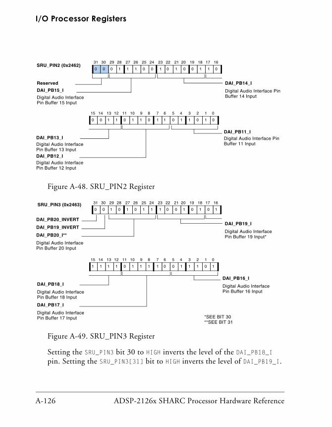
I/O Processor Registers
A-126 ADSP-2126x SHARC Processor Hardware Reference
Setting the SRU_PIN3 bit 30 to HIGH inverts the level of the DAI_PB18_I pin. Setting the SRU_PIN3[31] bit to HIGH inverts the level of DAI_PB19_I.
Figure A-48. SRU_PIN2 Register
Figure A-49. SRU_PIN3 Register
31 30 29 28 27 26 25 24 23 22 21 20 19 18 17 16
00 0 0 1 1 1 0 0 1 0 1 0 0 1 1
Reserved
15 14 13 12 11 10 9 8 7 6 5 4 3 2 1 0
00 0 1 1 0 1 1 0 1 1 0 1 1 0 1
Digital Audio Interface Pin Buffer 15 Input
DAI_PB15_I
DAI_PB13_I
Digital Audio Interface Pin Buffer 14 Input
DAI_PB14_I
Digital Audio Interface Pin Buffer 13 InputDAI_PB12_IDigital Audio Interface Pin Buffer 12 Input
Digital Audio Interface Pin Buffer 11 Input
DAI_PB11_I
SRU_PIN2 (0x2462)
31 30 29 28 27 26 25 24 23 22 21 20 19 18 17 16
10 0 1 0 1 0 1 1 1 0 0 1 0 1 0
DAI_PB20_INVERT
15 14 13 12 11 10 9 8 7 6 5 4 3 2 1 0
11 1 1 1 0 1 1 1 1 0 0 1 1 1 0
Digital Audio Interface Pin Buffer 20 Input
DAI_PB20_I**
DAI_PB18_I
Digital Audio Interface Pin Buffer 19 Input*
DAI_PB19_I
Digital Audio Interface Pin Buffer 18 Input
DAI_PB17_I
Digital Audio Interface Pin Buffer 17 Input
Digital Audio Interface Pin Buffer 16 Input
DAI_PB16_I
DAI_PB19_INVERT
*SEE BIT 30**SEE BIT 31
SRU_PIN3 (0x2463)

ADSP-2126x SHARC Processor Hardware Reference A-127
Registers Reference
If the SRU_PIN3[23:18] bits = 18, then setting SRU_PIN3[30] to HIGH does not invert the output. If the SRU_PIN3[29:24] bits = 19, then setting SRU_PIN3[31] to HIGH does not invert the output.
Table A-37. Group D Sources – Pin Signal Assignments
Selection Code Source Signal Description
000000 (0x0) DAI_PB01_O Select DAI Pin Buffer 1 as the source
000001 (0x1) DAI_PB02_O Select DAI Pin Buffer 2 as the source
000010 (0x2) DAI_PB03_O Select DAI Pin Buffer 3 as the source
000011 (0x3) DAI_PB04_O Select DAI Pin Buffer 4 as the source
000100 (0x4) DAI_PB05_O Select DAI Pin Buffer 5 as the source
000101 (0x5) DAI_PB06_O Select DAI Pin Buffer 6 as the source
000110 (0x6) DAI_PB07_O Select DAI Pin Buffer 7 as the source
000111 (0x7) DAI_PB08_O Select DAI Pin Buffer 8 as the source
001000 (0x8) DAI_PB09_O Select DAI Pin Buffer 9 as the source
001001 (0x9) DAI_PB10_O Select DAI Pin Buffer 10 as the source
001010 (0xA) DAI_PB11_O Select DAI Pin Buffer 11 as the source
001011 (0xB) DAI_PB12_O Select DAI Pin Buffer 12 as the source
001100 (0xC) DAI_PB13_O Select DAI Pin Buffer 13 as the source
001101 (0xD) DAI_PB14_O Select DAI Pin Buffer 14 as the source
001110 (0xE) DAI_PB15_O Select DAI Pin Buffer 15 as the source
001111 (0xF) DAI_PB16_O Select DAI Pin Buffer 16 as the source
010000 (0x10) DAI_PB17_O Select DAI Pin Buffer 17 as the source
010001 (0x11) DAI_PB18_O Select DAI Pin Buffer 18 as the source
010010 (0x12) DAI_PB19_O Select DAI Pin Buffer 19 as the source
010011 (0x13) DAI_PB20_O Select DAI Pin Buffer 20 as the source
010100 (0x14) SPORT0_DA_O Select SPORT 0A Data as the source
010101 (0x15) SPORT0_DB_O Select SPORT 0B Data as the source
010110 (0x16) SPORT1_DA_O Select SPORT 1A Data as the source

I/O Processor Registers
A-128 ADSP-2126x SHARC Processor Hardware Reference
010111 (0x17) SPORT1_DB_O Select SPORT 1B Data as the source
011000 (0x18) SPORT2_DA_O Select SPORT 2A Data as the source
011001 (0x19) SPORT2_DB_O Select SPORT 2B Data as the source
011010 (0x1A) SPORT3_DA_O Select SPORT 3A Data as the source
011011 (0x1B) SPORT3_DB_O Select SPORT 3B Data as the source
011100 (0x1C) SPORT4_DA_O Select SPORT 4A Data as the source
011101 (0x1D) SPORT4_DB_O Select SPORT 4B Data as the source
011110 (0x1E) SPORT5_DA_O Select SPORT 5A Data as the source
011111 (0x1F) SPORT5_DB_O Select SPORT 5B Data as the source
100000 (0x20) SPORT0_CLK_O Select SPORT 0 Clock as the source
100001 (0x21) SPORT1_CLK_O Select SPORT 1 Clock as the source
100010 (0x22) SPORT2_CLK_O Select SPORT 2 Clock as the source
100011 (0x23) SPORT3_CLK_O Select SPORT 3 Clock as the source
100100 (0x24) SPORT4_CLK_O Select SPORT 4 Clock as the source
100101 (0x25) SPORT5_CLK_O Select SPORT 5 Clock as the source
100110 (0x26) SPORT0_FS_O Select SPORT 0 Frame Sync as the source
100111 (0x27) SPORT1_FS_O Select SPORT 1 Frame Sync as the source
101000 (0x28) SPORT2_FS_O Select SPORT 2 Frame Sync as the source
101001 (0x29) SPORT3_FS_O Select SPORT 3 Frame Sync as the source
101010 (0x2A) SPORT4_FS_O Select SPORT 4 Frame Sync as the source
101011 (0x2B) SPORT5_FS_O Select SPORT 5 Frame Sync as the source
101100 (0x2C) TIMER0_O Select Timer 0 as the source
101101 (0x2D) TIMER1_O Select Timer 1 as the source
101110 (0x2E) TIMER2_O Select Timer 2 as the source
101111 (0x2F) FLAG10_O Select Flag 10 as the source1
Table A-37. Group D Sources – Pin Signal Assignments (Cont’d)
Selection Code Source Signal Description

ADSP-2126x SHARC Processor Hardware Reference A-129
Registers Reference
110000 (0x30) MISCB_2_O Select Miscellaneous Control B-2 as the source
110001 (0x31) MISCB_3_O Select Miscellaneous Control B-3 as the source
110010 (0x32) MISCB_4_O Select Miscellaneous Control B-4 as the source
110011 (0x33) MISCB_5_O Select Miscellaneous Control B-5 as the source
110100 (0x34) FLAG11_O Select Flag 11 as the source
110101 (0x35) FLAG12_O Select Flag 12 as the source
110110 (0x36) FLAG13_O Select Flag 13 as the source
110111 (0x37) FLAG14_O Select Flag 14 as the source
111000 (0x38) PCG_CLKA_O Select Precision Clock A as the source
111001 (0x39) PCG_CLKB_O Select Precision Clock B as the source
111010 (0x3A) PCG_FSA_O Select Precision Frame Sync A as the source
111011 (0x3B) PCG_FSB_O Select Precision Frame Sync B as the source
111100 (0x3C) FLAG15_O Select Flag 15 as the source
111101 (0x3D) Reserved
111110 (0x3E) LOW Select Logic Level Low (0) as the source
111111 (0x3F) HIGH Select Logic Level High (1) as the source
1 The ADSP-2126x SHARC processor supports 16 flags including: four pins in the IRQ, six pins (FLAG10-15) in the Digital Application Interface (DAI), and 16 address pins in the Parallel Port can act as flags. Parallel ports function as flags when the PPFLGS bit (bit 20) of the SYS-CTL register is set (= 1). This bit causes the 16 address pins to function as FLAG0–FLAG15. The IRQ acts as a flag that also generates an interrupt.
Table A-37. Group D Sources – Pin Signal Assignments (Cont’d)
Selection Code Source Signal Description

I/O Processor Registers
A-130 ADSP-2126x SHARC Processor Hardware Reference
Miscellaneous SRU Registers (SRU_EXT_MISCx, Group E)
The Miscellaneous Signal Routing registers are a very powerful and versa-tile feature of the DAI. These registers allow external pins, timers, and clocks to serve as interrupt sources or timer inputs and outputs. They also allow pins to connect to other pins, or to invert the logic of other pins. Note that MISCB2_I, MISCB3_I, MISCB4_I, and MISCB5_I may be mapped directly to the DAI pin buffers using Group D registers (see Table A-37).
The Miscellaneous Signal Routing registers correspond to the Group E miscellaneous signals listed in Table A-38. Thirty-two possible signal sources can be connected using these read/write registers:
• SRU_EXT_MISCA, described in Figure A-50 on page A-131
• SRU_EXT_MISCB, described in Figure A-51 on page -132

ADSP-2126x SHARC Processor Hardware Reference A-131
Registers Reference
Figure A-50. SRU_EXT_MISCA Register
31 30 29 28 27 26 25 24 23 22 21 20 19 18 17 16
10 0 1 1 1 1 0 1 1 1 1 0 1 1 1
INV_MISCA5_I
15 14 13 12 11 10 9 8 7 6 5 4 3 2 1 0
00 1 1 1 1 0 1 1 1 1 0 1 1 1 1
Invert Miscellaneous Channel A 4
INV_MISCA4_I
External Miscellaneous Channel A 3
MISCA3_IInvert Miscellaneous Channel A 5
External Miscellaneous Channel A 5
MISCA5_I**External Miscellaneous Channel A 4
MISCA4_I*
External Miscellaneous Channel A 2
MISCA2_IExternal Miscellaneous Channel A 0
MISCA0_I
External Miscellaneous Channel A 1
MISCA1_I
*SEE BIT 30**SEE BIT 31
DAI Interrupt 31DAI_INT_31
DAI Interrupt 30DAI_INT_30
Flag 15 InterruptFLAG15_I
DAI Interrupt 28DAI_INT_28
Flag 13 InterruptFLAG13_I
DAI Interrupt 29DAI_INT_29
Flag 14 InterruptFLAG14_I
SRU_EXT_MISCA (0x2470)
MISCA3_I
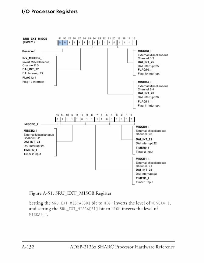
I/O Processor Registers
A-132 ADSP-2126x SHARC Processor Hardware Reference
Setting the SRU_EXT_MISCA[30] bit to HIGH inverts the level of MISCA4_I, and setting the SRU_EXT_MISCA[31] bit to HIGH inverts the level of MISCA5_I.
Figure A-51. SRU_EXT_MISCB Register
31 30 29 28 27 26 25 24 23 22 21 20 19 18 17 16
10 0 1 1 1 1 0 1 1 1 1 0 1 1 1
Reserved
15 14 13 12 11 10 9 8 7 6 5 4 3 2 1 0
00 1 1 1 1 0 1 1 1 1 0 1 1 1 1
Invert Miscellaneous Channel B 5
INV_MISCB5_I
External Miscellaneous Channel B 2
MISCB2_I External Miscellaneous Channel B 0
MISCB0_I
External Miscellaneous Channel B 1
MISCB1_I
DAI Interrupt 27DAI_INT_27
Flag 12 InterruptFLAG12_I
External Miscellaneous Channel B 3
MISCB3_I
External Miscellaneous Channel B 4
MISCB4_I
DAI Interrupt 25DAI_INT_25
Flag 10 InterruptFLAG10_I
DAI Interrupt 26DAI_INT_26
Flag 11 InterruptFLAG11_I
DAI Interrupt 22DAI_INT_22
TIMER0_I
DAI Interrupt 23DAI_INT_23
TIMER1_I
DAI Interrupt 24DAI_INT_24
TIMER2_I
SRU_EXT_MISCB (0x2471)
MISCB3_I
Timer 2 Input
Timer 1 Input
Timer 2 Input
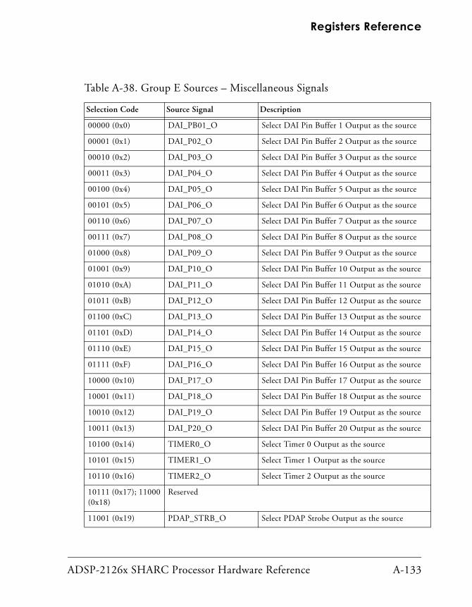
ADSP-2126x SHARC Processor Hardware Reference A-133
Registers Reference
Table A-38. Group E Sources – Miscellaneous Signals
Selection Code Source Signal Description
00000 (0x0) DAI_PB01_O Select DAI Pin Buffer 1 Output as the source
00001 (0x1) DAI_P02_O Select DAI Pin Buffer 2 Output as the source
00010 (0x2) DAI_P03_O Select DAI Pin Buffer 3 Output as the source
00011 (0x3) DAI_P04_O Select DAI Pin Buffer 4 Output as the source
00100 (0x4) DAI_P05_O Select DAI Pin Buffer 5 Output as the source
00101 (0x5) DAI_P06_O Select DAI Pin Buffer 6 Output as the source
00110 (0x6) DAI_P07_O Select DAI Pin Buffer 7 Output as the source
00111 (0x7) DAI_P08_O Select DAI Pin Buffer 8 Output as the source
01000 (0x8) DAI_P09_O Select DAI Pin Buffer 9 Output as the source
01001 (0x9) DAI_P10_O Select DAI Pin Buffer 10 Output as the source
01010 (0xA) DAI_P11_O Select DAI Pin Buffer 11 Output as the source
01011 (0xB) DAI_P12_O Select DAI Pin Buffer 12 Output as the source
01100 (0xC) DAI_P13_O Select DAI Pin Buffer 13 Output as the source
01101 (0xD) DAI_P14_O Select DAI Pin Buffer 14 Output as the source
01110 (0xE) DAI_P15_O Select DAI Pin Buffer 15 Output as the source
01111 (0xF) DAI_P16_O Select DAI Pin Buffer 16 Output as the source
10000 (0x10) DAI_P17_O Select DAI Pin Buffer 17 Output as the source
10001 (0x11) DAI_P18_O Select DAI Pin Buffer 18 Output as the source
10010 (0x12) DAI_P19_O Select DAI Pin Buffer 19 Output as the source
10011 (0x13) DAI_P20_O Select DAI Pin Buffer 20 Output as the source
10100 (0x14) TIMER0_O Select Timer 0 Output as the source
10101 (0x15) TIMER1_O Select Timer 1 Output as the source
10110 (0x16) TIMER2_O Select Timer 2 Output as the source
10111 (0x17); 11000 (0x18)
Reserved
11001 (0x19) PDAP_STRB_O Select PDAP Strobe Output as the source

I/O Processor Registers
A-134 ADSP-2126x SHARC Processor Hardware Reference
Setting the SRU_EXT_MISCA[30] bit to HIGH inverts the level of the EXT_MSCA_4 bit. Setting the SRU_EXT_MISCA[31] bit to HIGH inverts the level of the EXT_MISCA_5 bit.
DAI Pin Buffer Enable Registers (SRU_PBENx, Group F)
The Pin Enable Control registers activate the drive buffer for each of the 20 DAI pins. When the pins are not enabled (driven), they can be used as inputs. Each of the pin enables are connected, based on the 6-bit values in Table A-39. Sixty-four possible signal sources can be designated for these read/write registers:
• SRU_PBEN0, described in Figure A-52
• SRU_PBEN1, described in Figure A-53
• SRU_PBEN2, described in Figure A-54
• SRU_PBEN3, described in Figure A-55
11010 (0x1A) PCG_CLKA_O Select Precision Clock A Output as the source
11011 (0x1B) PCG_FSA_O Select Precision Frame Sync A Output as the source
11100 (0x1C) PCG_CLKB_O Select Precision Clock B Output as the source
11101 (0x1D) PCG_FSB_O Select Precision Frame Sync B Output as the source
11110 (0x1E) MISC_LOW_MISC_O Select Logic Level Low (0) as the source
11111 (0x1F) MISC_HIGH_MISC_O Select Logic Level High (1) as the source
Table A-38. Group E Sources – Miscellaneous Signals (Cont’d)
Selection Code Source Signal Description

ADSP-2126x SHARC Processor Hardware Reference A-135
Registers Reference
Figure A-52. SRU_PBEN0
Figure A-53. SRU_PBEN1
31 30 29 28 27 26 25 24 23 22 21 20 19 18 17 16
00 0 0 0 1 1 1 0 0 0 1 0 0 1 0
Reserved
15 14 13 12 11 10 9 8 7 6 5 4 3 2 1 0
01 0 0 0 0 0 1 0 1 1 0 0 1 0 1
DAI Port 5 Pin Buffer Enable Input
PBEN05
DAI Port 3 Pin Buffer Enable Input
PBEN03 DAI Port 1 Pin Buffer Enable Input
PBEN01
DAI Port 4 Pin Buffer Enable Input
PBEN04
DAI Port 2 Pin Buffer Enable Input
PBEN02
SRU_PBEN0 (0x2478)
31 30 29 28 27 26 25 24 23 22 21 20 19 18 17 16
00 0 0 1 0 0 1 1 0 0 1 0 1 0 0
Reserved
15 14 13 12 11 10 9 8 7 6 5 4 3 2 1 0
11 1 0 1 0 0 1 1 0 0 0 0 1 1 1
DAI Port 10 Pin Buffer Enable Input
PBEN10
DAI Port 8 Pin Buffer Enable Input
PBEN08 DAI Port 6 Pin Buffer Enable Input
PBEN06
DAI Port 8 Pin Buffer Enable Input
PBEN08
DAI Port 7 Pin Buffer Enable Input
PBEN07
SRU_PBEN1 (0x2479)
DAI Port 9 Pin Buffer Enable Input
PBEN09

I/O Processor Registers
A-136 ADSP-2126x SHARC Processor Hardware Reference
Figure A-54. SRU_PBEN2
Figure A-55. SRU_PBEN3
31 30 29 28 27 26 25 24 23 22 21 20 19 18 17 16
10 0 0 1 1 0 1 0 0 1 0 1 0 1 0
Reserved
15 14 13 12 11 10 9 8 7 6 5 4 3 2 1 0
00 1 0 0 0 1 0 1 1 1 0 1 0 1 1
DAI Port 15 Pin Buffer Enable Input
PBEN15
DAI Port 13 Pin Buffer Enable Input
PBEN13 DAI Port 11 Pin Buffer Enable Input
PBEN11
DAI Port 14 Pin Buffer Enable Input
PBEN14
DAI Port 12 Pin Buffer Enable Input
PBEN12
SRU_PBEN2 (0x247A)
31 30 29 28 27 26 25 24 23 22 21 20 19 18 17 16
10 0 0 1 1 1 0 1 0 1 1 1 0 0 0
Reserved
15 14 13 12 11 10 9 8 7 6 5 4 3 2 1 0
11 1 1 1 0 1 1 1 1 0 0 1 1 0 1
DAI Port 20 Pin Buffer Enable Input
PBEN20
DAI Port 18 Pin Buffer Enable Input
PBEN18 DAI Port 16 Pin Buffer Enable Input
PBEN16
DAI Port 19 Pin Buffer Enable Input
PBEN19
DAI Port 17 Pin Buffer Enable Input
PBEN17
SRU_PBEN3 (0x247B)

ADSP-2126x SHARC Processor Hardware Reference A-137
Registers Reference
Table A-39. Group F Sources – Pin Output Enable
Selection Code Source Signal Description
000000 (0x0) LOW Select Logic Level Low (0) as the source
000001 (0x1) HIGH Select Logic Level High (1) as the source
000010 (0x2) MISCA0_O Assign Miscellaneous Control A0 Output to a pin
000011 (0x3) MISCA1_O Assign Miscellaneous Control A1 Output to a pin
000100 (0x4) MISCA2_O Assign Miscellaneous Control A2 Output to a pin
000101 (0x5) MISCA3_O Assign Miscellaneous Control A3 Output to a pin
000110 (0x6) MISCA4_O Assign Miscellaneous Control A4 Output to a pin
000111 (0x7) MISCA5_O Assign Miscellaneous Control A5 Output to a pin
001000 (0x8) SPORT0_CLK_PBEN_O Select Serial Port 0 Clock Output Enable as the source
001001 (0x9) SPORT0_FS_PBEN_O Select Serial Port 0 Frame Sync Output Enable as the source
001010 (0xA) SPORT0_DA_PBEN_O Select Serial Port 0 Data Channel A Output Enable as the source
001011 (0xB) SPORT0_DB_PBEN_O Select Serial Port 0 Data Channel B Output Enable as the source
001100 (0xC) SPORT1_CLK_PBEN_O Select Serial Port 1 Clock Output Enable as the source
001101 (0xD) SPORT1_FS_PBEN_O Select Serial Port 1 Frame Sync Output Enable as the source
001110 (0xE) SPORT1_DA_PBEN_O Select Serial Port 1 Data Channel A Output Enable as the source
001111 (0xF) SPORT1_DB_PBEN_O Select Serial Port 1 Data Channel B Output Enable as the source
010000 (0x10) SPORT2_CLK_PBEN_O Select Serial Port 2 Clock Output Enable as the source
010001 (0x11) SPORT2_FS_PBEN_O Select Serial Port 2 Frame Sync Output Enable as the source
010010 (0x12) SPORT2_DA_PBEN_O Select Serial Port 2 Data Channel A Output Enable as the source

I/O Processor Registers
A-138 ADSP-2126x SHARC Processor Hardware Reference
010011 (0x13) SPORT2_DB_PBEN_O Select Serial Port 2 Data Channel B Output Enable as the source
010100 (0x14) SPORT3_CLK_PBEN_O Select Serial Port 3 Clock Output Enable as the source
010101 (0x15) SPORT3_FS_PBEN_O Select Serial Port 3 Frame Sync Output Enable as the source
010110 (0x16) SPORT3_DA_PBEN_O Select Serial Port 3 Data Channel A Output Enable as the source
010111 (0x17) SPORT3_DB_PBEN_O Select Serial Port 3 Data Channel B Output Enable as the source
011000 (0x18) SPORT4_CLK_PBEN_O Select Serial Port 4 Clock Output Enable as the source
011001 (0x19) SPORT4_FS_PBEN_O Select Serial Port 4 Frame Sync Output Enable as the source
011010 (0x1A) SPORT4_DA_PBEN_O Select Serial Port 4 Data Channel A Output Enable as the source
011011 (0x1B) SPORT4_DB_PBEN_O Select Serial Port 4 Data Channel B Output Enable as the source
011100 (0x1C) SPORT5_CLK_PBEN_O Select Serial Port 5 Clock as the Output Enable source
011101 (0x1D) SPORT5_FS_PBEN_O Select Serial Port 5 Frame Sync Output Enable as the source
011110 (0x1E) SPORT5_DA_PBEN_O Select Serial Port 5 Data Channel A Output Enable as the source
011111 (0x1F) SPORT5_DB_PBEN_O Select Serial Port 5 Data Channel B Output Enable as the source
100000 (0x20) TIMER0_PBEN_O Select Timer 0 Output Enable as the source
100001 (0x21) TIMER1_PBEN_O Select Timer 1 Output Enable as the source
100010 (0x22) TIMER2_PBEN_O Select Timer 2 Output Enable as the source
100011 (0x23) FLAG10_PBEN_O Select Flag 10 Output Enable as the source
100100 (0x24) FLAG11_PBEN_O Select Flag 11 Output Enable as the source
Table A-39. Group F Sources – Pin Output Enable (Cont’d)
Selection Code Source Signal Description

ADSP-2126x SHARC Processor Hardware Reference A-139
Registers Reference
Precision Clock Generator RegistersThe Precision Clock Generator (PCG) consists of two identical units. Each of these two units (A and B) generates one clock signal (CLKA_O or CLKB_O) and one frame sync (FSA_O or FSB_O) output. The PCGs are con-trolled by the following five memory-mapped registers in the DAI:
• PCG_CTLA_0, described in Figure A-56
• PCG_CTLA_1, described in Figure A-57
• PCG_CTLB_0, described in Figure A-58
• PCG_CTLB_1, described in Figure A-59
• PCG_PW, described in Figure A-60
100101 (0x25) FLAG12_PBEN_O Select Flag 12 Output Enable as the source
100110 (0x26) FLAG13_PBEN_O Select Flag 13 Output Enable as the source
100111 (0x27) FLAG14_PBEN_O Select Flag 14 Output Enable as the source
101000 (0x28) FLAG15_PBEN_O Select Flag 15 Output Enable as the source
101001 (0x29) Reserved
Table A-39. Group F Sources – Pin Output Enable (Cont’d)
Selection Code Source Signal Description

I/O Processor Registers
A-140 ADSP-2126x SHARC Processor Hardware Reference
Figure A-56. PCG_CTLA_0 Register
Table A-40. PCG_CTLA_0 Register Bit Descriptions
Bits Name Description
19–0 FSADIV Divisor for Frame Sync A.
29–20 FSAPHASE_HI Phase for Frame Sync A. Represents the upper half of the 20-bit value for the channel A frame sync phase. The phase represents the number of input clocks remaining in the first frame after the signal is enabled.See FSAPHASE_LO (Bits 29-20) in PCG_CTLA_1 described on on page A-141.
30 ENFSA Enable Frame Sync A.0 = Frame Sync A generation disabled1 = Frame Sync A generation enabled
31 ENCLKA Enable Clock A.0 = Clock A generation disabled1 = Clock A generation enabled
31 30 29 28 27 26 25 24 23 22 21 20 19 18 17 16
00 0 0 0 0 0 0 0 0 0 0 0 0 0 0
ENCLKA
15 14 13 12 11 10 9 8 7 6 5 4 3 2 1 0
00 0 0 0 0 0 0 0 0 0 0 0 0 0 0
Enable Clock A
Frame Sync A Divisor
FSADIV
Frame Sync A Phase 19:10
FSAPHASE_HI
ENFSAEnable Frame Sync A
PCG_CTLA_0 (0x24C0)

ADSP-2126x SHARC Processor Hardware Reference A-141
Registers Reference
Figure A-57. PCG_CTLA_1 Register
Table A-41. PCG_CTLA_1 Register Bit Descriptions
Bits Name Description
19–0 CLKADIV Divisor for Clock A.
29–20 FSAPHASE_LO Phase for Frame Sync A. Note: This field represents the lower half of the 20-bit value for the channel A frame sync phase. The phase represents the number of input clocks remaining in the first frame after the signal is enabled.See also FSAPHASE_HI (Bits 29-20) in PCG_CTLA_0 shown in on page A-140.
30 FSASOURCE Frame Sync A Source Master Clock Source for Frame Sync A.0 = CLKIN input selected for Frame Sync A1 = PCG_EXTA_I selected for Frame Sync A
31 CLKASOURCE Clock A Source Master Clock Source for Clock A.0 = CLKIN input selected for Clock A1 = PCG_EXTA_I selected for Clock A
31 30 29 28 27 26 25 24 23 22 21 20 19 18 17 16
00 0 0 0 0 0 0 0 0 0 0 0 0 0 0
CLKASOURCE
15 14 13 12 11 10 9 8 7 6 5 4 3 2 1 0
00 0 0 0 0 0 0 0 0 0 0 0 0 0 0
Clock A Source
CLK A DivisorCLKADIV
Frame Sync A Phase 9:0
FSAPHASE_LO
FSASOURCEFrame Sync A Source
PCG_CTLA_1 (0x24C1)

I/O Processor Registers
A-142 ADSP-2126x SHARC Processor Hardware Reference
Figure A-58. PCG_CTLB_0 Register
Table A-42. PCG_CTLB_0 Register Bit Descriptions
Bits Name Description
19–0 FSBDIV Divisor for Frame Sync B.
29–20 FSBPHASE_HI Phase for Frame Sync B. This field represents the upper half of the 20-bit value for the channel B frame sync phase. The phase represents the number of input clocks remaining in the first frame after the signal is enabled.See also FSBPHASE_LO (Bits 29-20) in PCG_CTLB_1 shown in Figure A-59 on page A-143.
30 ENFSB Enable Frame Sync B.0 = Frame Sync B generation disabled1 = Frame Sync B generation enabled
31 ENCLKB Enable Clock B.0 = Clock B generation disabled1 = Clock B generation enabled
31 30 29 28 27 26 25 24 23 22 21 20 19 18 17 16
00 0 0 0 0 0 0 0 0 0 0 0 0 0 0
ENCLKB
15 14 13 12 11 10 9 8 7 6 5 4 3 2 1 0
00 0 0 0 0 0 0 0 0 0 0 0 0 0 0
Enable Clock B
Frame Sync B Divisor
FSBDIV
Frame Sync B Phase 19:10
FSBPHASE_HI
ENFSBEnable Frame Sync B
PCG_CTLB_0 (0x24C2)

ADSP-2126x SHARC Processor Hardware Reference A-143
Registers Reference
Figure A-59. PCG_CTLB_1 Register
Table A-43. PCG_CTLB_1 Register Bit Descriptions
Bits Name Description
19–0 CLKBDIV Divisor for Clock B.
29–20 FSBPHASE_LO Phase for Frame Sync B. Note: This field represents the lower half of the 20-bit value for the channel B frame sync phase. The phase represents the number of input clocks remaining in the first frame after the signal is enabled.See also FSBPHASE_HI (Bits 29-20) in PCG_CTLB_0 shown in Figure A-58 on page A-142.
30 FSBSOURCE Frame Sync B Source. Master Clock Source for Frame Sync B.0 = CLKIN input selected for Frame Sync B1 = PCG_EXTB_I selected for Frame Sync B
31 CLKBSOURCE Clock B Source. Master Clock Source for Clock B.0 = CLKIN input selected for Clock B1 = PCG_EXTB_I selected for Clock B
31 30 29 28 27 26 25 24 23 22 21 20 19 18 17 16
00 0 0 0 0 0 0 0 0 0 0 0 0 0 0
CLKBSOURCE
15 14 13 12 11 10 9 8 7 6 5 4 3 2 1 0
00 0 0 0 0 0 0 0 0 0 0 0 0 0 0
Clock B Source
CLK B DivisorCLKBDIV
Frame Sync B Phase 9:0
FSBPHASE_LO
FSBSOURCEFrame Sync B Source
PCG_CTLB_1 (0x24C3)

I/O Processor Registers
A-144 ADSP-2126x SHARC Processor Hardware Reference
Figure A-60. PCG_PW Register (Bypass Mode)
Table A-44. PCG_PW Register (Bypass Mode)
Bits Name Description
0 STROBEA One Shot Frame Sync A. Frame sync is a pulse with duration equal to one period of MISCA2_I signal repeating at the beginning of every frame.Note: This is valid in bypass mode only.
1 INVFSA Active Low Frame Sync Select for Frame Sync A. Selects an active low FS if set, (= 1) or active high FS if cleared, (= 0).
15–2 Reserved1
16 STROBEB One Shot Frame Sync B. Frame Sync is a pulse with duration equal to one period of MISCA3_I signal repeating at the beginning of every frame.Note: This is valid in bypass mode only.
17 INVFSB Active Low Frame Sync Select. Selects an active low FS if set, (= 1) or active high FS if cleared, (= 0).
31–18 Reserved1
1 In bypass mode, Bits 15-2 and Bits 31-18 are ignored.
31 30 29 28 27 26 25 24 23 22 21 20 19 18 17 16
00 0 0 0 0 0 0 0 0 0 0 0 0 0 0
Reserved
15 14 13 12 11 10 9 8 7 6 5 4 3 2 1 0
00 0 0 0 0 0 0 0 0 0 0 0 0 0 0
One Shot Frame Sync B
STROBEB
INVFSBActive Low Frame Sync B
Reserved One Shot Frame Sync A
STROBEA
INVFSAActive Low Frame Sync A
PCG_PW (0x24C4)

ADSP-2126x SHARC Processor Hardware Reference A-145
Registers Reference
Figure A-61. PCG_PW Register (Normal Mode)
Table A-45. PCG_PW Register (Normal Mode)
Number of Bits Name Description
15–0 PWFSA Pulse Width for Frame Sync A. These bits are valid when not in Bypass mode.
31–16 PWFSB Pulse Width for Frame Sync B. These bits are valid when not in Bypass mode.
31 30 29 28 27 26 25 24 23 22 21 20 19 18 17 16
00 0 0 0 0 0 0 0 0 0 0 0 0 0 0
15 14 13 12 11 10 9 8 7 6 5 4 3 2 1 0
00 0 0 0 0 0 0 0 0 0 0 0 0 0 0
PWFSB
Pulse Width Frame Sync A
PWFSA
Pulse Width Frame Sync B
PCG_PW (0x24C4)
I/O Processor Registers
A-146 ADSP-2126x SHARC Processor Hardware Reference
Input Data Port RegistersThe Input Data Port (IDP) provides an additional input path to the pro-cessor core, configurable as 8 channels of serial data or 7 channels of serial data, and a single channel of up to a 20-bit wide parallel data. Seven regis-ters are used to specify modes, track status of inputs and outputs, permit the IDP FIFO buffer to be read, and so on.
• IDP_CTL, described in Figure A-62
• DAI_STAT, described in Figure A-70
• IDP_FIFO, described on Figure A-63
• IDP_DMA_Ix (including IDP_DMA_I0, IDP_DMA_I1, IDP_DMA_I2, IDP_DMA_I3, IDP_DMA_I4, IDP_DMA_I5, IDP_DMA_I6, and IDP_DMA_I7) described beginning with Figure A-64
• IDP_DMA_Mx (including IDP_DMA_M0, IDP_DMA_M1, IDP_DMA_M2, IDP_DMA_M3, IDP_DMA_M4, IDP_DMA_M5, IDP_DMA_M6, and IDP_DMA_M7), described beginning with Figure A-65
• IDP_DMA_Cx (including IDP_DMA_C0, IDP_DMA_C1, IDP_DMA_C2, IDP_DMA_C3, IDP_DMA_C4, IDP_DMA_C5, IDP_DMA_C6, and IDP_DMA_C7), described beginning with Figure A-66
• IDP_PDAP_CTL, described in Figure A-67

ADSP-2126x SHARC Processor Hardware Reference A-147
Registers Reference
Input Data Port Control Register (IDP_CTL)
The IDP_CTL[31:8] bits control the input format modes for each of the eight channels.
Figure A-62. IDP_CTL Register
Table A-46. IDP_CTL Register
Bits Name Description
3–0 IDP_NSET Monitored number of FIFO entries where N > samples raises Interrupt Controller bit 8.
4 IDP_BHD IDP Buffer Hang Disable. Reads of an empty FIFO or writes to a full FIFO make the core hang. This condition continues until the FIFO has valid data (in the case of reads) or the FIFO has at least one empty location (in the case of writes).1 = Core hang is disabled0 = Core hang is enabled
31 30 29 28 27 26 25 24 23 22 21 20 19 18 17 16
00 0 0 0 0 0 0 0 0 0 0 0 0 0 0
15 14 13 12 11 10 9 8 7 6 5 4 3 2 1 0
00 0 0 0 0 0 0 0 0 0 0 0 0 0 0
IDP_SMODE7
Buffer Hang Disable
IDP_SMODE6
IDP_SMODE3
IDP_SMODE4
IDP_SMODE5
IDP_SMODE2
IDP_SMODE1
IDP_SMODE0
IDP_ENABLE
IDP_NSET
IDP_BHD
IDP_DMA_EN
IDP_CLROVER
IDP_CTL (0x24B0)
Serial Mode Input Select 7
Serial Mode Input Select 6
Serial Mode Input Select 2
Serial Mode Input Select 1
Serial Mode Input Select 0
Input data port Enable
Serial Mode Input Select 3
Serial Mode Input Select 4
Serial Mode Input Select 5
Monitor FIFO Entries
IDP DMA Enable
Clear FIFO Overflow
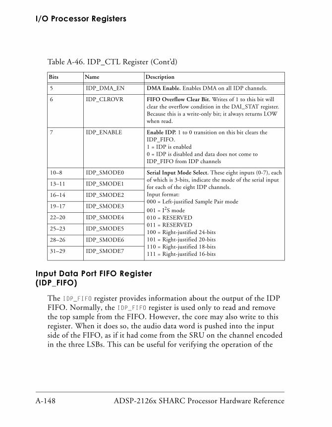
I/O Processor Registers
A-148 ADSP-2126x SHARC Processor Hardware Reference
Input Data Port FIFO Register (IDP_FIFO)
The IDP_FIFO register provides information about the output of the IDP FIFO. Normally, the IDP_FIFO register is used only to read and remove the top sample from the FIFO. However, the core may also write to this register. When it does so, the audio data word is pushed into the input side of the FIFO, as if it had come from the SRU on the channel encoded in the three LSBs. This can be useful for verifying the operation of the
5 IDP_DMA_EN DMA Enable. Enables DMA on all IDP channels.
6 IDP_CLROVR FIFO Overflow Clear Bit. Writes of 1 to this bit will clear the overflow condition in the DAI_STAT register. Because this is a write-only bit; it always returns LOW when read.
7 IDP_ENABLE Enable IDP. 1 to 0 transition on this bit clears the IDP_FIFO.1 = IDP is enabled0 = IDP is disabled and data does not come to IDP_FIFO from IDP channels
10–8 IDP_SMODE0 Serial Input Mode Select. These eight inputs (0-7), each of which is 3-bits, indicate the mode of the serial input for each of the eight IDP channels.Input format: 000 = Left-justified Sample Pair mode
001 = I2S mode010 = RESERVED011 = RESERVED100 = Right-justified 24-bits101 = Right-justified 20-bits110 = Right-justified 18-bits111 = Right-justified 16-bits
13–11 IDP_SMODE1
16–14 IDP_SMODE2
19–17 IDP_SMODE3
22–20 IDP_SMODE4
25–23 IDP_SMODE5
28–26 IDP_SMODE6
31–29 IDP_SMODE7
Table A-46. IDP_CTL Register (Cont’d)
Bits Name Description

ADSP-2126x SHARC Processor Hardware Reference A-149
Registers Reference
FIFO, the DMA channels, and the status portions of the IDP. The IDP FIFO is an eight-deep FIFO.
Channel encoding provides for eight combinations, corresponding to the eight inputs. When using Channels 1–7, this register format applies, as well as when using Channel 0 in Serial mode. When using Channel 0 in Parallel mode, refer to the descriptions of the four possible packing modes. For more information, see “Packing Unit” on page 11-8.
Figure A-63. IDP_FIFO Register
Table A-47. IDP_FIFO Register Bit Descriptions
Bits Name Description
2–0 IDP Channel Encoding Bits. Indicate serial input port channel number that gave this serial input data.Note: This information is not valid when data comes from PDAP channel.
3 LR_STAT Left/Right Channel Status. Indicate whether the data in bits 31–4 is the left or the right audio channel as dictated by the frame sync signal. The polarity of the encoding depends on the serial mode selected in IDP_SMODE for that channel. See IDP_CTL description in Table A-46 on page A-147.
31–4 Input Data (Serial). Some LSBs can be zero, depending on the mode.
31 30 29 28 27 26 25 24 23 22 21 20 19 18 17 16
00 0 0 0 0 0 0 0 0 0 0 0 0 0 0
15 14 13 12 11 10 9 8 7 6 5 4 3 2 1 0
00 0 0 0 0 0 0 0 0 0 0 0 0 0 0
SERIAL INPUT DATA
Indicates Serial Input Port Channel Number
IDP Channel Encoding Bits
Left/Right Channel as Specified by Frame Sync
LR_STAT
IDP_FIFO (0x24D0)

I/O Processor Registers
A-150 ADSP-2126x SHARC Processor Hardware Reference
The information in this table is not valid for the case where data comes from the PDAP channel.
Input Data Port DMA Control Registers
Each of the eight DMA channels have an I register with an Index pointer (19 bits), an M register with an M modifier/stride (6 bits), and a C regis-ter with a count (16 bits). For example, IDP_DMA_I0, IDP_DMA_M0 and IDP_DMA_C0 control the DMA for Channel 0. These registers are:
• IDP_DMA_Ix (Index) registers
• IDP_DMA_Mx (Modifier) registers
• IDP_DMA_Cx (Count) registers
Figure A-64. IDP_DMA_Ix Register
31 30 29 28 27 26 25 24 23 22 21 20 19 18 17 16
00 0 0 0 0 0 0 0 0 0 0 0 0 0 0
15 14 13 12 11 10 9 8 7 6 5 4 3 2 1 0
00 0 0 0 0 0 0 0 0 0 0 0 0 0 0
Reserved
Input Data Port DMA Channel Index
INDEX
IDP_DMA_Ix (0x2400–0x2407)

ADSP-2126x SHARC Processor Hardware Reference A-151
Registers Reference
Parallel Data Acquisition Port Control Register (IDP_PDAP_CTL)
Setting the IDP_PDAP_CTL[31] bit enables either the 20 DAI pins or the 16 parallel port address/data pins to be used as a parallel input channel. These parallel words may be packed into 32-bit words for efficiency. The data then flows through the FIFO and is transferred by a dedicated DMA channel into the core’s memory as with any IDP channel.
The IDP_PDAP_CTL register provides 20 mask bits that allow the input from any of the 20 pins to be ignored. When the mask bit is cleared, the corresponding bit is cleared in the acquired data word. This register also
Figure A-65. IDP_DMA_Mx Register
Figure A-66. IDP_DMA_Cx Register
31 30 29 28 27 26 25 24 23 22 21 20 19 18 17 16
00 0 0 0 0 0 0 0 0 0 0 0 0 0 0
15 14 13 12 11 10 9 8 7 6 5 4 3 2 1 0
00 0 0 0 0 0 0 0 0 0 0 0 0 0 0
Reserved
Input Data Port DMA Channel Modifier
MODIFIER
IDP_DMA_Mx (0x2410–0x2417)
31 30 29 28 27 26 25 24 23 22 21 20 19 18 17 16
00 0 0 0 0 0 0 0 0 0 0 0 0 0 0
15 14 13 12 11 10 9 8 7 6 5 4 3 2 1 0
00 0 0 0 0 0 0 0 0 0 0 0 0 0 0
Reserved
Input Data Port DMA Channel Counter
COUNTER
IDP_DMA_Cx (0x2420–0x2427)

I/O Processor Registers
A-152 ADSP-2126x SHARC Processor Hardware Reference
provides a reset bit that zeros any data waiting in the packing unit to be latched into the FIFO. The RESET bit (bit 30) causes the reset circuit to strobe when asserted, and then automatically clears. Therefore, this bit always returns a value of zero when read. Bit 26 of the IDP_PDAP_CTL regis-ter selects between the two sets of pins that may be used as the parallel input port. When the IDP_PDAP_CTL[26] bit is set, the upper 16 bits are read from the AD[15:Ø] pins. When the IDP_PDAP_CTL[26] bit is cleared, the upper 16 bits are read from the DAI_P[20:5] pins.
Note that the four LSB’s of the parallel data acquisition port input are not multiplexed, and this input value is always read from the DAI pins, DAI_P[4:1].
Figure A-67. IDP_PDAP_CTL Register
IDP_P12_PDAPMASK
31 30 29 28 27 26 25 24 23 22 21 20 19 18 17 16
00 0 0 0 0 0 0 0 0 0 0 0 0 0 0
15 14 13 12 11 10 9 8 7 6 5 4 3 2 1 0
00 0 0 0 0 0 0 0 0 0 0 0 0 0 0
Reserved
IDP_P16_PDAPMASK
IDP_PDAP_EN
IDP_P19_PDAPMASK
IDP_P18_PDAPMASK
IDP_P17_PDAPMASK
IDP_P15_PDAPMASK
IDP_P14_PDAPMASK
IDP_P13_PDAPMASK
IDP_P01_PDAPMASK
IDP_P02_PDAPMASK
IDP_P03_PDAPMASK
IDP_P04_PDAPMASK
IDP_P05_PDAPMASK
IDP_P06_PDAPMASKIDP_P11_PDAPMASK
IDP_P10_PDAPMASK
IDP_P09_PDAPMASK
IDP_P07_PDAPMASK
IDP_P08_PDAPMASK
IDP_PDAP_RESET
IDP_PDAP_CLKEDGE
IDP_PDAP_PACKINGX
IDP_PORT_SELECT
IDP_P20_PDAPMASK

ADSP-2126x SHARC Processor Hardware Reference A-153
Registers Reference
Table A-48. IDP_PDAP_CTL Register
Bits Name Description
0 IDP_P01_PDAPMASK Parallel Data Acquisition Port Mask0 = Input data from DAI_01 is masked1 = Input data from DAI_01 is un-masked
1 IDP_P02_PDAPMASK Parallel Data Acquisition Port Mask0 = Input data from DAI_02 is masked1 = Input data from DAI_02 is un-masked
2 IDP_P03_PDAPMASK Parallel Data Acquisition Port Mask0 = Input data from DAI_03 is masked1 = Input data from DAI_03 is un-masked
3 IDP_P04_PDAPMASK Parallel Data Acquisition Port Mask0 = Input data from DAI_04 is masked1 = Input data from DAI_04 is un-masked
4 IDP_P05_PDAPMASK Parallel Data Acquisition Port Mask0 = Input data from DAI_05/DATA0 is masked1 = Input data from DAI_05/DATA0 is un-masked
5 IDP_P06_PDAPMASK Parallel Data Acquisition Port Mask0 = Input data from DAI_06/DATA1 is masked1 = Input data from DAI_06/DATA1 is un-masked
6 IDP_P07_PDAPMASK Parallel Data Acquisition Port Mask0 = Input data from DAI_07/DATA2 is masked1 = Input data from DAI_07/DATA2 is un-masked
7 IDP_P08_PDAPMASK Parallel Data Acquisition Port Mask0 = Input data from DAI_08/DATA3 is masked1 = Input data from DAI_08/DATA3 is un-masked
8 IDP_P09_PDAPMASK Parallel Data Acquisition Port Mask0 = Input data from DAI_09/DATA4 is masked1 = Input data from DAI_09/DATA4 is un-masked
9 IDP_P10_PDAPMASK Parallel Data Acquisition Port Mask0 = Input data from DAI_10/DATA5 is masked1 = Input data from DAI_10/DATA5 is un-masked
10 IDP_P11_PDAPMASK Parallel Data Acquisition Port Mask0 = Input data from DAI_11/DATA6 is masked1 = Input data from DAI_11/DATA6 is un-masked
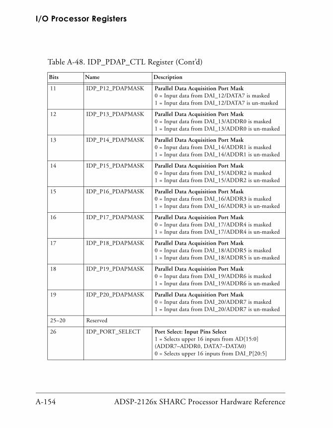
I/O Processor Registers
A-154 ADSP-2126x SHARC Processor Hardware Reference
11 IDP_P12_PDAPMASK Parallel Data Acquisition Port Mask0 = Input data from DAI_12/DATA7 is masked1 = Input data from DAI_12/DATA7 is un-masked
12 IDP_P13_PDAPMASK Parallel Data Acquisition Port Mask0 = Input data from DAI_13/ADDR0 is masked1 = Input data from DAI_13/ADDR0 is un-masked
13 IDP_P14_PDAPMASK Parallel Data Acquisition Port Mask0 = Input data from DAI_14/ADDR1 is masked1 = Input data from DAI_14/ADDR1 is un-masked
14 IDP_P15_PDAPMASK Parallel Data Acquisition Port Mask0 = Input data from DAI_15/ADDR2 is masked1 = Input data from DAI_15/ADDR2 is un-masked
15 IDP_P16_PDAPMASK Parallel Data Acquisition Port Mask0 = Input data from DAI_16/ADDR3 is masked1 = Input data from DAI_16/ADDR3 is un-masked
16 IDP_P17_PDAPMASK Parallel Data Acquisition Port Mask0 = Input data from DAI_17/ADDR4 is masked1 = Input data from DAI_17/ADDR4 is un-masked
17 IDP_P18_PDAPMASK Parallel Data Acquisition Port Mask0 = Input data from DAI_18/ADDR5 is masked1 = Input data from DAI_18/ADDR5 is un-masked
18 IDP_P19_PDAPMASK Parallel Data Acquisition Port Mask0 = Input data from DAI_19/ADDR6 is masked1 = Input data from DAI_19/ADDR6 is un-masked
19 IDP_P20_PDAPMASK Parallel Data Acquisition Port Mask0 = Input data from DAI_20/ADDR7 is masked1 = Input data from DAI_20/ADDR7 is un-masked
25–20 Reserved
26 IDP_PORT_SELECT Port Select: Input Pins Select1 = Selects upper 16 inputs from AD[15:0] (ADDR7–ADDR0, DATA7–DATA0)0 = Selects upper 16 inputs from DAI_P[20:5]
Table A-48. IDP_PDAP_CTL Register (Cont’d)
Bits Name Description

ADSP-2126x SHARC Processor Hardware Reference A-155
Registers Reference
Peripheral Timer RegistersThe timer peripheral module provides general-purpose timer functional-ity. It consists of three identical timer units. Each timer has memory-mapped registers described in the following sections.
28–27 IDP_PDAP_PACKING PACKINGSelects PDAP packing mode00 = 8 to 32 packing01 = {11,11,10} to 32 packing10 = 16 to 32 packing11 = 20 to 32 packing
29 IDP_PDAP_CLKEDGE PDAP (Rising or Falling) Clock EdgeSetting this bit (= 1) causes the data to be latched on the falling edge. Clearing this bit causes data to be latched on the rising edge of the clock (IDP0_CLK_I).
30 IDP_PDAP_RESET PDAP Reset Setting this bit (= 1) causes the PDAP reset circuit to strobe; then this bit is cleared automat-ically. This bit will always return a value of zero when read.
31 IDP_PDAP_EN PDAP Enable Setting this bit (= 1) enables either the 20 DAI pins or the 16 parallel port address/data pins to be used as a parallel input channel. Clearing this bit (= 0) disables those pins from use as parallel input channels.Note: When this bit is set to 1, then IDP Channel 0 cannot be used as a serial input port.
Table A-48. IDP_PDAP_CTL Register (Cont’d)
Bits Name Description

I/O Processor Registers
A-156 ADSP-2126x SHARC Processor Hardware Reference
Timer Configuration Registers (TMxCTL)
All timer clocks are gated off when the specific timer’s configuration regis-ter is set to zero at system reset or subsequently reset by user programs. These registers are shown in Figure A-68.
Figure A-68. TMxCTL Register
Table A-49. TMxCTL Register Bit Descriptions
Bit Name Definition
1–0 TIMODE Timer Mode.00 = Reset01 = PWM_OUT mode (TIMODEPWM)10 = WDTH_CAP mode (TIMODEW)11 = EXT_CLK mode (TIMODEEXT)
2 PULSE Pulse Edge Select.1 = Positive active pulse0 = Negative active pulse
3 PRDCNT Period Count.1 = Count to end of period0 = Count to end of width
4 IRQEN Interrupt Enable.1 = Enable0 = Disable
TIMODE (1–0)
Interrupt Enable
PRDCNTPulse Edge Select
Timer Mode
PULSE
Period Count
IRQEN
15 14 13 12 11 10 9 8 7 6 5 4 3 2 1 0

ADSP-2126x SHARC Processor Hardware Reference A-157
Registers Reference
Timer Status Registers (TMxSTAT)
The global status registers TMxSTAT are shown in Figure A-69. Status bits are sticky and require a write-one to clear operation. During a status regis-ter read access, all reserved or unused bits return a zero. Each timer generates a unique processor interrupt request signal, TIMxIRQ.
A common status register latches these interrupts. Interrupt bits are sticky and must be cleared to assure that the interrupt is not reissued.
Each timer is provided with its own sticky status register TIMxEN bit. To enable or disable an individual timer, the TIMxEN bit is set or cleared. For example, writing a one to bit 8 sets the TIM0EN bit; writing a one to bit 9 clears it. Writing a one to both bit 8 and bit 9 clears TIM0EN. Reading the status register returns the TIM0EN state on both bit 8 and bit 9. The remaining TIMxEN bits operate similarly.
Figure A-69. TMxSTAT Register
Table A-50. TMxSTAT Register Bit Descriptions
Bit Name Description
0 TIM0IRQ Timer 0 Interrupt Latch Write one-to-clear (also an output)
1 TIM1IRQ Timer 1 Interrupt Latch Write one-to-clear (also an output)
TIM1DIS (W1C)
TIM1ENTimer 1 Disable
Timer 1 EnableTIM0DIS (W1C)
TIM0EN
Timer 0 Disable
Timer 0 Enable
TIM0IRQ (W1C)Timer 0 Interrupt
TIM2IRQ (W1C)Timer 2 Interrupt
TIM0OVFTimer 0 CounterOverflow Error
TIM1OVFTimer 1 CounterOverflow Error
15 14 13 12 11 10 9 8 7 6 5 4 3 2 1 0
TIM2DIS (W1C)
TIM2ENTimer 2 Disable
Timer 2 EnableTIM1IRQ (W1C)Timer 1 Interrupt
TIM2OVFTimer 1 Counter Overflow Error

I/O Processor Registers
A-158 ADSP-2126x SHARC Processor Hardware Reference
DAI RegistersThe digital applications interface (DAI) is comprised of a group of periph-erals and the signal routing unit (SRU).
Digital Audio Interface Status Register (DAI_STAT)
The DAI_STAT register is a read-only register located at address 0x24B8. The state of all eight DMA channels is reflected in the IDP_DMAx_STAT bits (bits 24–17) of the DAI_STAT register. These bits are set once the IDP_DMA_EN bit is set and they remain set until the last data in that channel is transferred. Even if the IDP_DMA_EN bit is set, it goes low once the required number of data transfers occurs. Even if the DMA through some channel is not intended, its IDP_DMAx_STAT goes high.
2 TIM2IRQ Timer 2 Interrupt Latch Write one-to-clear (also an output)
3 Reserved
4 TIM0OVF Timer 0 Overflow/Error Write one-to-clear (also an output)
5 TIM1OVF Timer 1 Overflow/Error Write one-to-clear (also an output)
6 TIM2OVF Timer 2 Overflow/Error Write one-to-clear (also an output)
7 Reserved
8 TIM0EN Timer 0 Enable Write one to enable timer 0
9 TIM0EN Timer 0 Disable Write one to disable timer 0
10 TIM1EN Timer 1 Enable Write one to enable timer 1
11 TIM1EN Timer 1 Disable Write one to disable timer 1
12 TIM2EN Timer 2 Enable Write one to enable timer 2
13 TIM2EN Timer 2 Disable Write one to disable timer 2
31–11 Reserved
Table A-50. TMxSTAT Register Bit Descriptions (Cont’d)
Bit Name Description
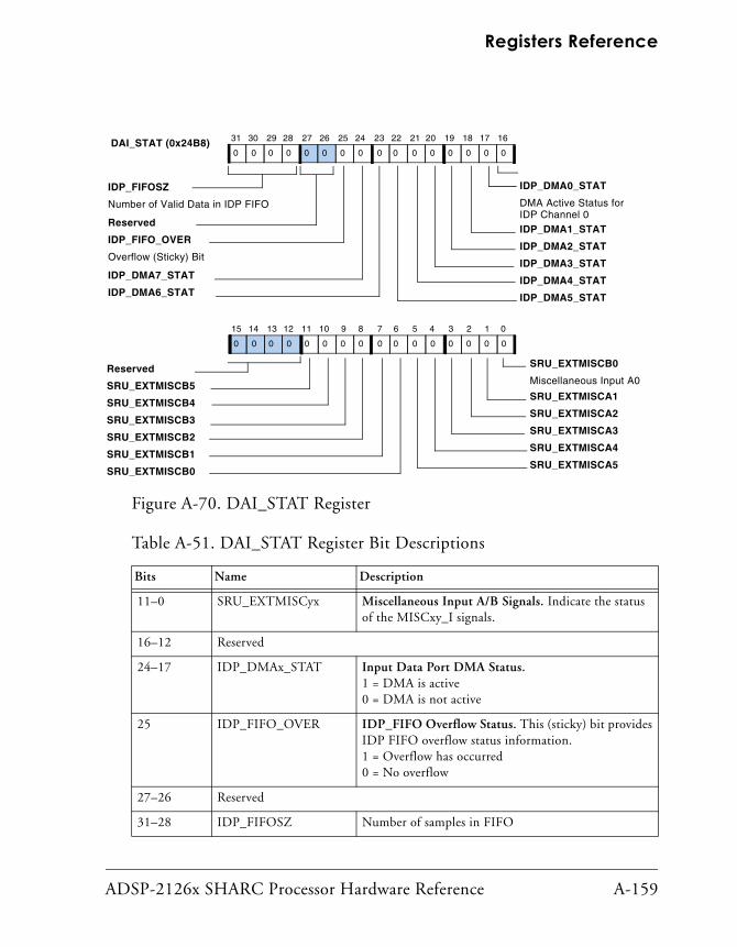
ADSP-2126x SHARC Processor Hardware Reference A-159
Registers Reference
Figure A-70. DAI_STAT Register
Table A-51. DAI_STAT Register Bit Descriptions
Bits Name Description
11–0 SRU_EXTMISCyx Miscellaneous Input A/B Signals. Indicate the status of the MISCxy_I signals.
16–12 Reserved
24–17 IDP_DMAx_STAT Input Data Port DMA Status.1 = DMA is active0 = DMA is not active
25 IDP_FIFO_OVER IDP_FIFO Overflow Status. This (sticky) bit provides IDP FIFO overflow status information.1 = Overflow has occurred0 = No overflow
27–26 Reserved
31–28 IDP_FIFOSZ Number of samples in FIFO
31 30 29 28 27 26 25 24 23 22 21 20 19 18 17 16
00 0 0 0 0 0 0 0 0 0 0 0 0 0 0
15 14 13 12 11 10 9 8 7 6 5 4 3 2 1 0
00 0 0 0 0 0 0 0 0 0 0 0 0 0 0
IDP_FIFOSZ
Miscellaneous Input A0
Reserved
SRU_EXTMISCB5
Number of Valid Data in IDP FIFO
IDP_FIFO_OVER
Overflow (Sticky) Bit
IDP_DMA7_STAT
IDP_DMA6_STAT
IDP_DMA3_STAT
IDP_DMA4_STAT
IDP_DMA1_STAT
IDP_DMA2_STAT
IDP_DMA0_STAT
DMA Active Status for IDP Channel 0
IDP_DMA5_STAT
Reserved
SRU_EXTMISCB4
SRU_EXTMISCB3
SRU_EXTMISCB2
SRU_EXTMISCB1
SRU_EXTMISCB0
SRU_EXTMISCA1
SRU_EXTMISCA2
SRU_EXTMISCA3
SRU_EXTMISCA4
SRU_EXTMISCA5SRU_EXTMISCB0
DAI_STAT (0x24B8)

I/O Processor Registers
A-160 ADSP-2126x SHARC Processor Hardware Reference
DAI Resistor Pull-up Enable Register (DAI_PIN_PULLUP)
This 20-bit read/write register is located at address 0x247D. Bits 19–0 of this register control the enabling/disabling 22.5 KΩ pull-up resistor on the DAI_P0[19:0] bits. Setting a bit to one enables a pull-up resistor on the corresponding pin. After RESET, the value of this register is 0xFFFFF, which means pull-up is enabled on all 20 DAI pins.
Figure A-71. DAI_PIN_PULLUP Register
Table A-52. DAI_PIN_PULLUP Register
Bits Name Description
0 DAI_P01_PULLUP Enable/Disable 22.5 KΩ Pull-up Resistor for DAI_P011 = enables pull-up on DAI_P010 = disables pull-up on DAI_P01
1 DAI_P02_PULLUP Enable/Disable 22.5 KΩ Pull-up Resistor for DAI_P021 = enables pull-up on DAI_P020 = disables pull-up on DAI_P02
2 DAI_P03_PULLUP Enable/Disable 22.5 KΩ Pull-up Resistor for DAI_P031 = enables pull-up on DAI_P030 = disables pull-up on DAI_P03
31 30 29 28 27 26 25 24 23 22 21 20 19 18 17 16
10 0 0 0 0 0 0 0 0 0 0 0 1 1 1
15 14 13 12 11 10 9 8 7 6 5 4 3 2 1 0
11 1 1 1 1 1 1 1 1 1 1 1 1 1 1
Reserved
DAI_P16_PULLUP
DAI_P20_PULLUP DAI_P19_PULLUP
DAI_P18_PULLUP
DAI_P17_PULLUP
DAI_P15_PULLUP
DAI_P14_PULLUP
DAI_P13_PULLUP
DAI_P12_PULLUP
DAI_P01_PULLUP
DAI_P02_PULLUP
DAI_P03_PULLUP
DAI_P04_PULLUP
DAI_P05_PULLUP
DAI_P06_PULLUPDAI_P11_PULLUP
DAI_P10_PULLUP
DAI_P09_PULLUP
DAI_P07_PULLUP
DAI_P08_PULLUP
DAI_PIN_PULLUP(0x247D)

ADSP-2126x SHARC Processor Hardware Reference A-161
Registers Reference
3 DAI_P04_PULLUP Enable/Disable 22.5 KΩ Pull-up Resistor for DAI_P041 = enables pull-up on DAI_P040 = disables pull-up on DAI_P04
4 DAI_P05_PULLUP Enable/Disable 22.5 KΩ Pull-up Resistor for DAI_P051 = enables pull-up on DAI_P050 = disables pull-up on DAI_P05
5 DAI_P06_PULLUP Enable/Disable 22.5 KΩ Pull-up Resistor for DAI_P061 = enables pull-up on DAI_P060 = disables pull-up on DAI_P06
6 DAI_P07_PULLUP Enable/Disable 22.5 KΩ Pull-up Resistor for DAI_P071 = enables pull-up on DAI_P070 = disables pull-up on DAI_P07
7 DAI_P08_PULLUP Enable/Disable 22.5 KΩ Pull-up Resistor for DAI_P081 = enables pull-up on DAI_P080 = disables pull-up on DAI_P08
8 DAI_P09_PULLUP Enable/Disable 22.5 KΩ Pull-up Resistor for DAI_P091 = enables pull-up on DAI_P090 = disables pull-up on DAI_P09
9 DAI_P10_PULLUP Enable/Disable 22.5 KΩ Pull-up Resistor for DAI_P101 = enables pull-up on DAI_P100 = disables pull-up on DAI_P10
10 DAI_P11_PULLUP Enable/Disable 22.5 KΩ Pull-up Resistor for DAI_P111 = enables pull-up on DAI_P110 = disables pull-up on DAI_P11
11 DAI_P12_PULLUP Enable/Disable 22.5 KΩ Pull-up Resistor for DAI_P121 = enables pull-up on DAI_P120 = disables pull-up on DAI_P12
12 DAI_P13_PULLUP Enable/Disable 22.5 KΩ Pull-up Resistor for DAI_P131 = enables pull-up on DAI_P130 = disables pull-up on DAI_P13
13 DAI_P14_PULLUP Enable/Disable 22.5 KΩ Pull-up Resistor for DAI_P141 = enables pull-up on DAI_P140 = disables pull-up on DAI_P14
Table A-52. DAI_PIN_PULLUP Register (Cont’d)
Bits Name Description

I/O Processor Registers
A-162 ADSP-2126x SHARC Processor Hardware Reference
14 DAI_P15_PULLUP Enable/Disable 22.5 KΩ Pull-up Resistor for DAI_P151 = enables pull-up on DAI_P150 = disables pull-up on DAI_P15
15 DAI_P16_PULLUP Enable/Disable 22.5 KΩ Pull-up Resistor for DAI_P161 = enables pull-up on DAI_P160 = disables pull-up on DAI_P16
16 DAI_P17_PULLUP
Enable/Disable 22.5 KΩ Pull-up Resistor for DAI_P171 = enables pull-up on DAI_P170 = disables pull-up on DAI_P17
17 DAI_P18_PULLUP Enable/Disable 22.5 KΩ Pull-up Resistor for DAI_P181 = enables pull-up on DAI_P180 = disables pull-up on DAI_P18
18 DAI_P19_PULLUP Enable/Disable 22.5 KΩ Pull-up Resistor for DAI_P191 = enables pull-up on DAI_P190 = disables pull-up on DAI_P19
19 DAI_P20_PULLUP Enable/Disable 22.5 KΩ Pull-up Resistor for DAI_P201 = enables pull-up on DAI_P200 = disables pull-up on DAI_P20
31–20 Reserved
Table A-52. DAI_PIN_PULLUP Register (Cont’d)
Bits Name Description

ADSP-2126x SHARC Processor Hardware Reference A-163
Registers Reference
DAI Pin Status Register (DAI_PIN_STAT)
This 20-bit read-only register is located at address 0x24B9. Bits 19–0 of this register indicate the status of DAI_P[20:1]. Reads from bits 31–20 always return 0. This register is updated at ½ core clock rate.
Figure A-72. DAI_PIN_STAT Register
Table A-53. DAI_PIN_STAT Register
Bits Name Description
0 DAI_P01 Provides status of DAI_P01 pin
1 DAI_P02 Provides status of DAI_P01 pin
2 DAI_P03 Provides status of DAI_P03 pin
3 DAI_P04 Provides status of DAI_P04 pin
4 DAI_P05 Provides status of DAI_P05 pin
5 DAI_P06 Provides status of DAI_P06 pin
31 30 29 28 27 26 25 24 23 22 21 20 19 18 17 16
10 0 0 0 0 0 0 0 0 0 0 0 1 1 1
15 14 13 12 11 10 9 8 7 6 5 4 3 2 1 0
11 1 1 1 1 1 1 1 1 1 1 1 1 1 1
Reserved
DAI_P16
DAI_P20 DAI_P19
DAI_P18
DAI_P17
DAI_P15
DAI_P14
DAI_P13
DAI_P12
DAI_P01
DAI_P02
DAI_P03
DAI_P04
DAI_P05
DAI_P06DAI_P11
DAI_P10
DAI_P09
DAI_P07
DAI_P08
DAI_PIN_STAT (0x24B9)

I/O Processor Registers
A-164 ADSP-2126x SHARC Processor Hardware Reference
DAI Interrupt Controller Registers
The DAI contains its own Interrupt Controller that indicates to the core when DAI audio peripheral related events occur. Since audio events gener-ally occur infrequently relative to the SHARC processor core, the DAI Interrupt Controller reduces all of its interrupts onto two interrupt signals within the core’s primary interrupt systems—one mapped with low prior-ity and one mapped with high priority. This architecture allows the user to indicate priority broadly. In this way, the DAI interrupt controller reg-isters provide 32 independently configurable interrupts labeled DAI_INT[31:0], respectively.
6 DAI_P07 Provides status of DAI_P07 pin
7 DAI_P08 Provides status of DAI_P08 pin
8 DAI_P09 Provides status of DAI_P09 pin
9 DAI_P10 Provides status of DAI_P10 pin
10 DAI_P11 Provides status of DAI_P11 pin
11 DAI_P12 Provides status of DAI_P12 pin
12 DAI_P13 Provides status of DAI_P13 pin
13 DAI_P14 Provides status of DAI_P14 pin
14 DAI_P15 Provides status of DAI_P15 pin
15 DAI_P16 Provides status of DAI_P16 pin
16 DAI_P17 Provides status of DAI_P17 pin
17 DAI_P18 Provides status of DAI_P18 pin
18 DAI_P19 Provides status of DAI_P19 pin
19 DAI_P20 Provides status of DAI_P20 pin
31–20 Reserved
Table A-53. DAI_PIN_STAT Register (Cont’d)
Bits Name Description

ADSP-2126x SHARC Processor Hardware Reference A-165
Registers Reference
The DAI Interrupt Controller is configured using three registers. Each of the 32 interrupt lines can be independently configured to trigger based on the incoming signal’s rising edge, falling edge, both or neither. Setting a bit in the DAI_IRPTL_RE or DAI_IRPTL_FE registers enables the interrupt level on the rising and falling edges, respectively.
The 32 interrupt signals within the DAI are mapped to two interrupt sig-nals in the primary Interrupt Controller of the SHARC processor core. The DAI_IRPTL_PRI register selects if the DAI interrupt is mapped to the high priority or low priority core interrupt (1 = high priority, 0 = low priority).
The DAI_IRPTL_H register is a read-only register that has bits set for every DAI interrupt latched for the high priority core interrupt. The DAI_IRPTL_L register is a read-only register that has bits set for every DAI interrupt latched for the low priority core interrupt. When a DAI inter-rupt occurs, the low or high priority core ISR should query its corresponding register to determine which of the 32 interrupt sources requires service. When the DAI_IRPTL_H register is read, the high priority latched interrupts are cleared. When the DAI_IRPTL_L register is read, the low priority latched interrupts are cleared.
DMA, overflow, and greater than N interrupts can be sensed only at rising edges. Falling edges are not used for these ten interrupts (eight DMA, one overflow, and one FIFO valid data greater than N).
The IDP_FIFO_GTN_INT interrupt is not cleared when the DAI_IRPTL_H/L registers are read. This interrupt is cleared automat-ically when the situation that caused of the interrupt goes away.

I/O Processor Registers
A-166 ADSP-2126x SHARC Processor Hardware Reference
The following registers are used primarily to provide status of the Resident Interrupt Controller:
• High Priority Interrupt Latch (DAI_IRPTL_H) register, described on page A-166
• Low Priority Interrupt Latch (DAI_IRPTL_L) register, described on page A-167
• Core Interrupt Priority Assignment (DAI_IRPTL_PRI) register, described on page A-168
• Rising Edge Interrupt Mask (DAI_IRPTL_RE) register, described on page A-169
• Falling Edge Interrupt Mask (DAI_IRPTL_FE) register, described on page A-170
Figure A-73. DAI_IRPTL_H Register
31 30 29 28 27 26 25 24 23 22 21 20 19 18 17 16
00 0 0 0 0 0 0 0 0 0 0 0 0 0 0
15 14 13 12 11 10 9 8 7 6 5 4 3 2 1 0
00 0 0 0 0 0 0 0 0 0 0 0 0 0 0
Reserved
IDP_DMA5_INT
SRU_EXTMISCA3_INT
ISRU_EXTMISCB1_INT
IDP_DMA7_INT
IDP_DMA6_INT
IDP_DMA4_INT
IDP_DMA3_INT
IDP_DMA2_INT
IDP_DMA1_INT
Reserved
IDP_FIFO_OVR_INT
ISRU_EXTMISCB0_INT
SRU_EXTMISCA2_INT
SRU_EXTMISCA1_INT
SRU_EXTMISCA0_INT
SRU_EXTMISCB5_INT
SRU_EXTMISCB4_INT
SRU_EXTMISCB3_INT
ISRU_EXTMISCB2_INT
IDP_DMA0_INT
IDP_FIFO_GTN_INTIDP FIFO Samples Exceeded Interrupt
IDP FIFO Overflow Interrupt
DAI_IRPTL_H (0x2488)

ADSP-2126x SHARC Processor Hardware Reference A-167
Registers Reference
An explicit read resets these register values to zero, except for the IDP_FIFO_GTN_INT (IDP FIFO samples exceeded interrupt) bit. The inter-rupt on the IDP_FIFO_GTN_INT bit clears automatically when the condition that caused the interrupt goes away.
A read resets the value to zero, except under the following condition—the IDP_FIFO_GTN_INT bit is not cleared when DAI_IRPTL_H/L registers are read. This bit is cleared when the cause of this interrupt is zero.
Figure A-74. DAI_IRPTL_L Register
31 30 29 28 27 26 25 24 23 22 21 20 19 18 17 16
00 0 0 0 0 0 0 0 0 0 0 0 0 0 0
15 14 13 12 11 10 9 8 7 6 5 4 3 2 1 0
00 0 0 0 0 0 0 0 0 0 0 0 0 0 0
Reserved
IDP_DMA5_INT
SRU_EXTMISCA3_INT
ISRU_EXTMISCB1_INT
IDP_DMA7_INT
IDP_DMA6_INT
IDP_DMA4_INT
IDP_DMA3_INT
IDP_DMA2_INT
IDP_DMA1_INT
Reserved
IDP_FIFO_OVR_INT
ISRU_EXTMISCB0_INT
SRU_EXTMISCA2_INT
SRU_EXTMISCA1_INT
SRU_EXTMISCA0_INT
SRU_EXTMISCB5_INT
SRU_EXTMISCB4_INT
SRU_EXTMISCB3_INT
ISRU_EXTMISCB2_INT
IDP_DMA0_INT
IDP_FIFO_GTN_INTIDP FIFO Samples Exceeded Interrupt
IDP FIFO Overflow Interrupt
DAI_IRPTL_L (0x2489)

I/O Processor Registers
A-168 ADSP-2126x SHARC Processor Hardware Reference
Figure A-75. DAI_IRPTL_PRI Register
31 30 29 28 27 26 25 24 23 22 21 20 19 18 17 16
00 0 0 0 0 0 0 0 0 0 0 0 0 0 0
15 14 13 12 11 10 9 8 7 6 5 4 3 2 1 0
00 0 0 0 0 0 0 0 0 0 0 0 0 0 0
Reserved
IDP_DMA5_INT
SRU_EXTMISCA3_INT
ISRU_EXTMISCB1_INT
IDP_DMA7_INT
IDP_DMA6_INT
IDP_DMA4_INT
IDP_DMA3_INT
IDP_DMA2_INT
IDP_DMA1_INT
Reserved
IDP_FIFO_OVR_INT
ISRU_EXTMISCB0_INT
SRU_EXTMISCA2_INT
SRU_EXTMISCA1_INT
SRU_EXTMISCA0_INT
SRU_EXTMISCB5_INT
SRU_EXTMISCB4_INT
SRU_EXTMISCB3_INT
ISRU_EXTMISCB2_INT
IDP_DMA0_INT
IDP_FIFO_GTN_INT
IDP FIFO Samples Exceeded Interrupt
IDP FIFO Overflow Interrupt
DAI_IRPTL_PRI (0x2484)
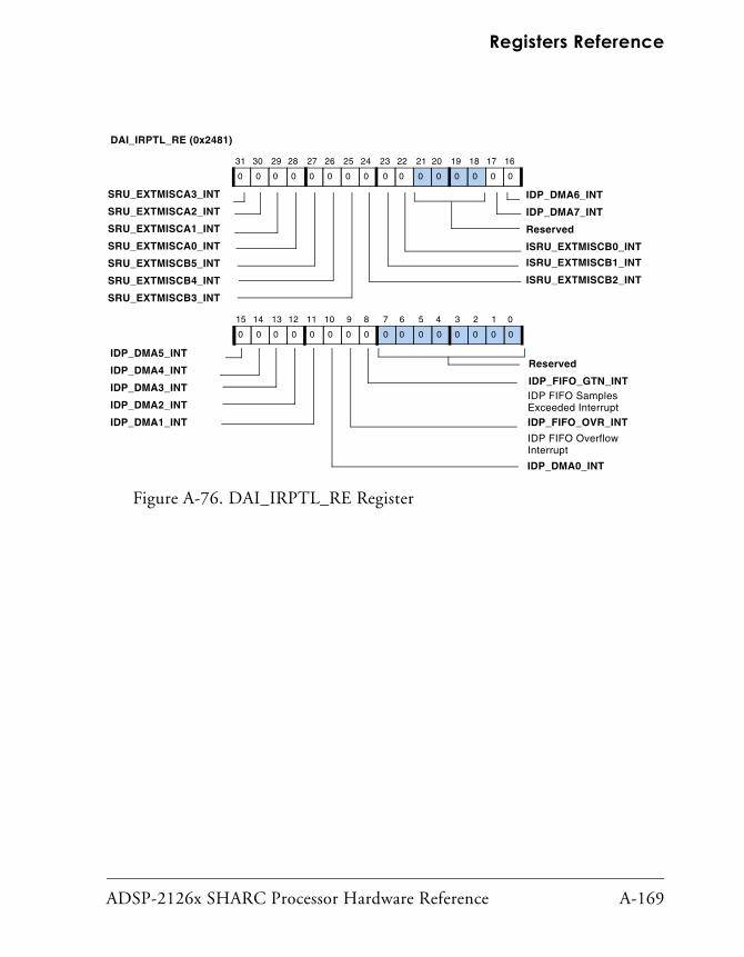
ADSP-2126x SHARC Processor Hardware Reference A-169
Registers Reference
Figure A-76. DAI_IRPTL_RE Register
31 30 29 28 27 26 25 24 23 22 21 20 19 18 17 16
00 0 0 0 0 0 0 0 0 0 0 0 0 0 0
15 14 13 12 11 10 9 8 7 6 5 4 3 2 1 0
00 0 0 0 0 0 0 0 0 0 0 0 0 0 0
Reserved
IDP_DMA5_INT
SRU_EXTMISCA3_INT
ISRU_EXTMISCB1_INT
IDP_DMA7_INT
IDP_DMA6_INT
IDP_DMA4_INT
IDP_DMA3_INT
IDP_DMA2_INT
IDP_DMA1_INT
Reserved
IDP_FIFO_OVR_INT
ISRU_EXTMISCB0_INT
SRU_EXTMISCA2_INT
SRU_EXTMISCA1_INT
SRU_EXTMISCA0_INT
SRU_EXTMISCB5_INT
SRU_EXTMISCB4_INT
SRU_EXTMISCB3_INT
ISRU_EXTMISCB2_INT
IDP_DMA0_INT
IDP_FIFO_GTN_INTIDP FIFO Samples Exceeded Interrupt
IDP FIFO Overflow Interrupt
DAI_IRPTL_RE (0x2481)

I/O Processor Registers
A-170 ADSP-2126x SHARC Processor Hardware Reference
Figure A-77. DAI_IRPTL_FE Register
31 30 29 28 27 26 25 24 23 22 21 20 19 18 17 16
00 0 0 0 0 0 0 0 0 0 0 0 0 0 0
15 14 13 12 11 10 9 8 7 6 5 4 3 2 1 0
00 0 0 0 0 0 0 0 0 0 0 0 0 0 0
Reserved
IDP_DMA5_INT
SRU_EXTMISCA3_INT
ISRU_EXTMISCB1_INT
IDP_DMA7_INT
IDP_DMA6_INT
IDP_DMA4_INT
IDP_DMA3_INT
IDP_DMA2_INT
IDP_DMA1_INT
Reserved
IDP_FIFO_OVR_INT
ISRU_EXTMISCB0_INT
SRU_EXTMISCA2_INT
SRU_EXTMISCA1_INT
SRU_EXTMISCA0_INT
SRU_EXTMISCB5_INT
SRU_EXTMISCB4_INT
SRU_EXTMISCB3_INT
ISRU_EXTMISCB2_INT
Reserved
IDP_FIFO_GTN_INTIDP FIFO Samples Exceeded Interrupt
IDP FIFO Overflow Interrupt
DAI_IRPTL_FE (0x2480)

ADSP-2126x SHARC Processor Core Manual -1
B INTERRUPT VECTOR ADDRESSES
Table B-2 shows all the ADSP-2126x processor interrupts, listed accord-ing to their bit position in the IRPTL, LIRPTL, and IMASK registers. For more information, see “Interrupt Latch Register (IRPTL)” on page A-23, “Interrupt Register (LIRPTL)” on page A-29, and “Interrupt Mask Regis-ter (IMASK)” on page A-24. Also shown is the address of the interrupt vector. Each vector is separated by four memory locations. The addresses in the vector table represent offsets from a base address. For an Interrupt Vector Table in internal RAM, the base address is 0x8 0000 and for inter-nal ROM, the base address is 0xA 0000. These are 48-bit addresses.
The interrupt name column in Table B-2 lists a mnemonic name for each interrupt as they are defined by the definitions file (def2126x.h) that comes with the software development tools.
SPI has only one interrupt for both transmit and receive.
Each serial port (SPORT) has only one interrupt for both transmit and receive.
Table B-1. Interrupt Vector Table Base Address
Address1
1 These are 48-bit addresses.
Description
0x0008 0000 Internal RAM
0x000A 0000 Internal ROM

-2 ADSP-2126x SHARC Processor Core Manual
Table B-2. ADSP-2126x Interrupt Vector Addresses
Register IRPTL/ IMASK, LIRPTL Bit#
Vector Address
Interrupt Name
Function
IRPTL 0 0x00 EMUI Emulator (read-only, non-mask-able); HIGHEST PRIORITY
IRPTL 1 0x04 RSTI Reset (read-only, non-maskable)
IRPTL 2 0x08 IICDI Illegal Input Condition Detected
IRPTL 3 0x0C SOVFI Status loop or mode stack over-flow; or PC stack full
IRPTL 4 0x10 TMZHI Timer = 0 (high priority option)
IRPTL 5 0x14 Reserved
IRPTL 6 0x18 BKPI Hardware Breakpoint Interrupt
IRPTL 7 0x1C Reserved
IRPTL 8 0x20 IRQ2I IRQ2I_ is asserted
IRPTL 9 0x24 IRQ1I IRQ1I_ is asserted
IRPTL 10 0x28 IRQ0I IRQ0I_ is asserted
IRPTL 11 0x2C DAIHI DAI High Priority Interrupt
IRPTL 12 0x30 SPIHI SPI Transmit or Receive (higher priority option)
IRPTL 13 0x34 GPTMR0I General-purpose IOP Timer 0 Interrupt
IRPTL 14 0x38 SP1I SPORT1 Interrupt
IRPTL 15 0x3C SP3I SPORT3 Interrupt
IRPTL 16 0x40 SP5I SPORT5 Interrupt
LIRPTL 0 0x44 SP0I SPORT0 Interrupt
LIRPTL 1 0x48 SP2I SPORT2 Interrupt
LIRPTL 2 0x4C SP4I SPORT4 Interrupt
LIRPTL 3 0x50 PPI Parallel Port Interrupt

ADSP-2126x SHARC Processor Core Manual -3
LIRPTL 4 0x54 GPTMR1I General-purpose IOP Timer 1 Interrupt
LIRPTL 5 0x58 -- Reserved
LIRPTL 6 0x5C DAILI DAI Low Priority Interrupt
LIRPTL 7 0x60 -- Reserved
IRPTL 17, 18, 19 0x64-0x6F -- Reserved
LIRPTL 8 0x70 GPTMR2I General-purpose IOP Timer 2 Interrupt
LIRPTL 9 0X74 SPILI SPI Transmit or Receive (lower priority option)
IRPTL 20 0x78 CB7I Circular Buffer 7 Overflow
IRPTL 21 0x7C CB15I Circular Buffer 15 Overflow
IRPTL 22 0x80 TMZLI Timer=0(Low Priority Option)
IRPTL 23 0x84 FIXI Fixed-point Overflow
IRPTL 24 0x88 FLTOI Floating-point Overflow Excep-tion
IRPTL 25 0x8C FLTUI Floating-point Underflow Excep-tion
IRPTL 26 0x90 FLTII Floating-point invalid exception
IRPTL 27 0x94 EMULI Emulator Low Priority Interrupt
IRPTL 28 0x98 SFT0I User Software Interrupt 0
IRPTL 29 0x9C SFT1I User Software Interrupt 1
IRPTL 30 0xA0 SFT2I User Software Interrupt 2
IRPTL 31 0xA4 SFT3I User Software Interrupt 3; LOW-EST PRIORITY
Table B-2. ADSP-2126x Interrupt Vector Addresses (Cont’d)
Register IRPTL/ IMASK, LIRPTL Bit#
Vector Address
Interrupt Name
Function

-4 ADSP-2126x SHARC Processor Core Manual

ADSP-2126x SHARC Processor Core Manual -1
G GLOSSARY
Autobuffering Unit (ABU). See I/O processor on page -5 and DMA on page -3.
Arithmetic Logic Unit (ALU). This part of a processing element performs arithmetic and logic operations on fixed-point and floating-point data.
Auxiliary registers. See Index Registers on page -5.
Base address. The starting address of a circular buffer to which the DAG wraps around. This address is stored in a DAG Bx register.
Base registers. A base (Bx) register is a Data Address Generator (DAG) register that sets up the starting address for a circular buffer.
Bit-reverse addressing. The Data Address Generator (DAG) provides a bit-reversed address during a data move without reversing the stored address.
Block repeat. See Do/Until instructions in the ADSP-21160 DSP Instruc-tion Set Reference.
Block size register. See Length Registers on page -6.
Broadcast data moves. The Data Address Generator (DAG) performs dual data moves to complementary registers in each processing element to sup-port SIMD mode.
Buffered serial port. See Serial ports on page -9.

-2 ADSP-2126x SHARC Processor Core Manual
Bus slave or slave mode. A DSP can be a bus slave to another DSP or to a host processor. The DSP becomes a host bus slave when the HBG signal is returned.
Circular buffer addressing. The DAG uses the Ix, Mx and Lx register set-tings to constrain addressing to a range of addresses. This range contains data that the DAG steps through repeatedly, “wrapping around” to repeat stepping through the range of addresses in a circular pattern.
Companding (compressing/expanding). This is the process of logarithmi-cally encoding and decoding data to minimize the number of bits that must be sent.
Conditional branches. These are JUMP or CALL/return instructions whose execution is based on testing an IF condition.
DAGEN, Data address generator. See Data Address Generator (DAG).
Data Address Generator (DAG). The data address generators (DAGs) provide memory addresses when data is transferred between memory and registers.
Data register file. This is the set of data registers that transfer data between the data buses and the computation units. These registers also provide local storage for operands and results.
Data registers (Dreg). These are registers in the PEx and PEy processing elements. These registers are hold operands for multiplier, ALU, or shifter operations and are denoted as Rx when used for fixed point operations or Fx when used for floating-point operations.
Deadlock Resolution. When both the DSP subsystem and the system try to access each other’s bus in the same cycle, a deadlock may occur in which neither access can complete. Techniques for resolving deadlock vary with the interface: DRAM, host, or multiprocessor DSP.
Delayed branches. These are JUMPS and CALL/return instructions with the delayed branches (DB) modifier. In delayed branches, no instruction

ADSP-2126x SHARC Processor Core Manual -3
cycles are lost in the pipeline, because the DSP executes the two instruc-tions after the branch while the pipeline fills with instructions from the new branch.
Denormal operands. When the biased exponent is zero, smaller numbers can only be represented by making the integer bit (and perhaps other lead-ing bits) of the significant zero. The numbers in this range are called denormalized (or tiny) numbers. The use of leading zeros with denormal-ized numbers allows smaller numbers to be represented.
Direct branches. These are JUMP or CALL/return instructions that use an absolute—not changing at runtime—address (such as a program label) or use a PC-relative address.
Direct reads & writes. A direct access of the DSP's internal memory or I/O processor registers by another DSP or by a host processor.
DMA (Direct Memory Accessing). The DSP’s I/O processor supports DMA of data between DSP memory and external memory, host, or peripherals through the external, link, and serial ports. Each DMA opera-tion transfers an entire block of data.
DMA chaining. The DSP supports chaining together multiple DMA sequences. In chained DMA, the I/O processor loads the next Transfer Control Block (DMA parameters) into the DMA parameter registers when the current DMA finishes and auto-initializes the next DMA sequence.
DMA Parameter Registers. These registers function similarly to data address generator registers, setting up a memory access process. These reg-isters include Internal Index registers (IISPX, IISPI), Internal Modify registers (IMSPI), Count registers (CSPx, CSPI), Chain Pointer registers (CPSPI), External Index registers (EIPP), External Modify registers (EMPP), and External Count registers (ECPP).
DMA TCB chain loading. This is the process that the I/O processor uses for loading the TCB of the next DMA sequence into the parameter regis-ters during chained DMA.

-4 ADSP-2126x SHARC Processor Core Manual
Edge-sensitive interrupt. The DSP detects this type of interrupt if the input signal is high (inactive) on one cycle and low (active) on the next cycle when sampled on the rising edge of CLKIN.
Endian Format, Little Versus Big. The DSP uses big-endian format—moves data starting with most-significant-bit and finishing with least-sig-nificant-bit—in almost all instances. The two exceptions are bit order for data transfer through the serial port and word order for packing through the parallel port. For compatibility with little-endian (least-signifi-cant-first) peripherals, the DSP supports both big- and little-endian bit order data transfers. Also for compatibility little endian hosts, the DSP supports both big and little endian word order data transfers.
Explicit Versus Implicit operations. In SIMD mode, identical instruc-tions execute on the PEx and PEy computational units; the difference is the data. The data registers for PEy operations are identified (implicitly) from the PEx registers in the instruction. This implicit relation between PEx and PEy data registers corresponds to complementary register pairs.
Field deposit (Fdep) instructions. These shifter instructions take a group of bits from the input register (starting at the LSB of the 32-bit integer field) and deposit the bits as directed anywhere within the result register.
Field extract (Fext) instructions. These shifter extract a group of bits as directed from anywhere within the input register and place them in the result register (aligned with the LSB of the 32-bit integer field).
Programmable Flag pins. These pins (FLAGx) can be programmed as input or output pins using bit settings in the MODE2 register. The status of the flag pins is given in the FLAGS or IOFLAG register.
General purpose input/output pins. See Programmable Flag pins.
Flag update. The DSP’s update to status flags occurs at the end of the cycle in which the status is generated and is available on the next cycle.

ADSP-2126x SHARC Processor Core Manual -5
Harvard architecture. DSPs use memory architectures that have separate buses for program and data storage. The two buses let the DSP get a data word and an instruction simultaneously.
Hold time cycle. This is an inactive bus cycle that the DSP automatically generates at the end of a read or write (depending on the parallel port access mode) to allow a longer hold time for address and data. The address—and data, if a write—remains unchanged and is driven for one cycle after the read or write strobes are deasserted.
I/O processor register. One of the control, status, or data buffer registers of the DSP's on-chip I/O processor.
Idle cycle. This is an inactive bus cycle that the DSP automatically gener-ates (depending on the parallel port access mode) to avoid data bus driver conflicts. Such a conflict can occur when a device with a long output dis-able time continues to drive after RD is deasserted while another device begins driving on the following cycle.
IDLE. An instruction that causes the processor to cease operations, hold-ing its current state until an interrupt occurs. Then, the processor services the interrupt and continues normal execution.
Index registers. An index register is a Data Address Generator (DAG) reg-ister that holds an address and acts as a pointer to memory.
Indirect branches. These are JUMP or CALL/return instructions that use a dynamic—changes at runtime—address that comes from the PM data address generator.
Inexact flags. An inexact flag is an exception flag whose bit position is inexact.
Interleaved data. To take advantage of the DSP’s data accesses to 4- and 3-column locations, programs must adjust the interleaving of data into (not necessarily sequential) memory locations to accommodate the mem-ory access mode.

-6 ADSP-2126x SHARC Processor Core Manual
Internal memory space. This space ranges from address 0x0000 0000 through 0x0005 3FFF (Normal word). Internal memory space refers to the DSP’s on-chip SRAM and memory mapped registers.
Interrupts. Subroutines in which a runtime event (not an instruction) triggers the execution of the routine.
JTAG port. This port supports the IEEE standard 1149.1 Joint Test Action Group (JTAG) standard for system test. This standard defines a method for serially scanning the I/O status of each component in a system.
Jumps. Program flow transfers permanently to another part of program memory.
Length registers. A length registers is a Data Address Generator (DAG) register that sets up the range of addresses a circular buffer.
Level-sensitive interrupts. The DSP detects this type of interrupt if the signal input is low (active) when sampled on the rising edge of CLKIN.
Loops. One sequence of instructions executes several times with zero overhead.
McBSP, Multichannel buffered serial port. See Serial port.
MCM, Multichannel mode. See Multichannel mode on page -9.
Memory Access Modes. The DSP supports Asynchronous external mem-ory space. In asynchronous access mode, the DSP’s RD and WR strobes change before CLKIN edge. In synchronous access mode, the DSP’s RD and WR strobes change on CLKIN edge.
Memory blocks and banks. The DSP’s internal memory is divided into blocks that are each associated with different data address generators. The DSP’s external memory spaces is divided into banks, which may be addressed by either data address generator.

ADSP-2126x SHARC Processor Core Manual -7
Modified addressing. The DAG generates an address that is incremented by a value or a register.
Modify address. The Data Address Generator (DAG) increments the stored address without performing a data move.
Modify registers. A modify register is a Data Address Generator (DAG) register that provides the increment or step size by which an index register is pre- or post-modified during a register move.
Multichannel Mode. In this mode, each data word of the serial bit stream occupies a separate channel.
Multifunction computations. Using the many parallel data paths within its computational units, the DSP supports parallel execution of multiple computational instructions. These instructions complete in a single cycle, and they combine parallel operation of the multiplier and the ALU or dual ALU functions. The multiple operations perform the same as if they were in corresponding single-function computations.
Multiplier. This part of a processing element does floating-point and fixed-point multiplication and executes fixed-point multiply/add and multiply/subtract operations.
Nonzero numbers. Nonzero, finite numbers are divided into two classes: normalized and denormalized
Neighbor Registers. In Long word addressed accesses, the DSP moves data to or from two neighboring data registers. The least-significant-32 bits moves to or from the explicit (named) register in the neighbor register pair. In forced Long word accesses (Normal word address with LW mne-monic), the DSP converts the Normal word address to Long word, placing the even Normal word location in the explicit register and the odd Nor-mal word location in the other register in the neighbor pair.
Parallel port. This port extends the DSPs internal address and data buses off-chip, providing the processor’s interface to off-chip memory devices.

-8 ADSP-2126x SHARC Processor Core Manual
PAGEN, Program address generation logic. “Chapter 3, Program Sequencer.
Peripherals. This refers to everything outside the processor core. The ADSP-2126x processor’s peripherals include internal memory, parallel port, I/O processor, JTAG port, and any external devices that connect to the DSP.
Precision. The precision of a floating-point number depends on the num-ber of bits after the binary point in the storage format for the number. The DSP supports two high precision floating-point formats: 32-bit IEEE single-precision floating-point (which uses 8 bits for the exponent and 24 bits for the mantissa) and a 40-bit extended precision version of the IEEE format.
Post-modify addressing. The Data Address Generator (DAG) provides an address during a data move and auto-increments the stored address for the next move.
Pre-modify addressing. The Data Address Generator (DAG) provides a modified address during a data move without incrementing the stored address.
Registers swaps. This special type of register-to-register move instruction uses the special swap operator, <->. A register-to-register swap occurs when registers in different processing elements exchange values.
Saturation (ALU saturation mode). In this mode, all positive fixed-point overflows return the maximum positive fixed-point number (0x7FFF FFFF), and all negative overflows return the maximum negative number (0x8000 0000).
Semaphore. This is a flag that can be read and written by any of the pro-cessors sharing the resource. Semaphores can be used in multiprocessor systems to allow the processors to share resources such as memory or I/O. The value of the semaphore tells the processor when it can access the

ADSP-2126x SHARC Processor Core Manual -9
resource. Semaphores are also useful for synchronizing the tasks being per-formed by different processors in a multiprocessing system.
Serial ports. The DSP has six synchronous serial ports that provide an inexpensive interface to a wide variety of digital and mixed-signal periph-eral devices.
SHARC. This is an acronym for Super Harvard Architecture. This DSP architecture balances a high performance processor core with high perfor-mance buses (PM, DM, I/O).
Shifter. This part of a processing element completes logical shifts, arith-metic shifts, bit manipulation, field deposit, and field extraction operations on 32-bit operands. Also, the Shifter can derive exponents.
SMUL, Saturation on multiplication. See Multiplier on page -7.
S/PDIF. (Sony/Philips Digital InterFace) A serial interface for transferring digital audio between devices such as CD and DVD players and amplifi-ers. S/PDIF is the consumer version of the AES/EBU interface and uses unbalanced 75 ohm coaxial cable with RCA or BNC connectors.
SST, Saturation on store. See Multiplier on page -7.
Subroutines. The processor temporarily interrupts sequential flow to exe-cute instructions from another part of program memory.
TADD, TDM address. See Multichannel Mode on page -7.
TCB chain loading. The process in which the DSP's DMA controller downloads a Transfer Control Block from memory and autoinitializes the DMA parameter registers.
Time Division Multiplexed (TDM) mode. The serial ports support TDM or multichannel operations. In multichannel mode, each data word of the serial bit stream occupies a separate channel— each word belongs to the next consecutive channel so that, for example, a 24-word block of data contains one word for each of 24 channels.

-10 ADSP-2126x SHARC Processor Core Manual
Transfer control block (TCB). A set of DMA parameter register values stored in memory that are downloaded by the DSP's DMA controller for chained DMA operations.
Tristate Versus Three-state. Analog Devices documentation uses the term “three-state” instead of “tristate” because Tristate™ is a trademarked term, which is owned by National Semiconductor.
Universal registers (Ureg). These are any processing element registers (data registers), any Data Address Generator (DAG) registers, any pro-gram sequencer registers, and any I/O processor registers.
Von Neumann architecture. This is the architecture used by most (non-DSP) microprocessors. This architecture uses a single address and data bus for memory access.
Wait states. The time spent waiting for an operation to take place. It may refer to a variable length of time a program has to wait before it can be processed, or to a fixed duration of time, such as a machine cycle.
When memory is too slow to respond to the CPU’s request for it, wait states are introduced until the memory can catch up.

ADSP-2126x SHARC Processor Hardware Reference I-1
I INDEX
Numerics16-bit floating-point format, 2-516-bit mode, 8-9, 8-11, 8-1416-bit to 32-bit word packing enable (PACK),
9-5432-bit data, normal word, 5-2632-bit shift registers, A-9832-bit single-precision floating-point format,
2-440-bit extended precision, 1-340-bit extended-precision floating-point format,
2-564-bit signed fixed-point product, 2-88-bit mode, 8-9, 8-11, 8-14
AABS function, 2-16absolute address, 3-12, G-3AC (ALU fixed-point carry) bit, A-12AC bit, 2-18, 3-19access to SPI registers, 10-34A channel See TXSP5A registeractive edge, defined, 10-5active low versus active high frame syncs, 9-36active state multichannel receive frame sync
select See LMFS bitAD1855 stereo DAC, power down, 10-7ADD instruction, 2-16, 2-43additional literature, -xxxivaddress
latch enable See also ALE pin
address bus, 1-2address fields, A-32address generator, 7-26addressing
even short words, 5-31odd short words, 5-31See post-modify, modify, bit-reverse, or
circular bufferstoring top-of-loop addresses, 3-16, A-32with DAGs, 4-10
ADSP-2126x processorconfigured as slave device, 10-6design advantages, 1-1enhancements, 1-13processor core, 1-5
AF (ALU floating point operation) bit, A-14AF bit, 2-18AI (ALU floating-point invalid operation) bit,
A-13AI bit, 2-18AIS (ALU floating-point invalid) bit, A-17AIS bit, 2-18A-law companding See companding
(compressing/expanding)ALE
cycle, 8-5pin, 8-3
aligning data, 5-13alternate DAG registers, 4-6alternate registers See also secondary registers,
1-8

Index
I-2 ADSP-2126x SHARC Processor Hardware Reference
ALU(AOS) bit, 2-18carry (AC) bit, 2-18, 3-19, A-12fixed-point overflow (AOS) bit, A-17floating-point operation (AF) bit, 2-18,
A-14result zero (AZ) bit, A-12saturation (ALUSAT) bit, A-6 See also arithmetic logic unit, 2-1x-input sign (AS) bit, 2-18, A-12zero (AZ) bit, 2-18
ALUSAT bit, 2-11, 2-17AN (ALU result negative) bit, 2-18, A-12AND, logical, 2-16AND breakpoints (ANDBKP) bit, A-49,
A-52AOS (ALU fixed-point overflow) bit, 2-18,
A-17Arithmetic Logic Unit (ALU), 1-5, 2-16
instructions, 2-16, 2-19interrupts, 3-55operations, 2-17saturation, 2-17status, 2-11, 2-15, 2-17, 2-18, 2-27, 3-55
arithmetic operations, 1-3, 2-16, 2-17arithmetic shifts, G-9arithmetic status (ASTATx/y) registers,
2-15AS (ALU x-input sign) bit, A-12AS bit, 2-18ASTATx/y registers, 2-15asymmetric data moves, 2-46asynchronous
access mode, G-6audience, intended, xxxiAUS (ALU floating-point underflow) bit,
A-17AUS bit, 2-18AV (ALU overflow) bit, A-12AV bit, 2-18, 3-19
average instructions, 2-16, 2-43AVS (ALU floating-point overflow) bit,
A-17AVS bit, 2-18AZ (ALU result zero or floating-point
underflow) bit, A-12AZ bit, 2-18
Bbackground registers See secondary registersbackground telemetry, 6-3background telemetry channel (BTC), 6-4barrel shifter See shifterbase (Bx) registers, 4-2, 4-17, A-37, G-1baud rate
See BAUDR bit See SPIBAUD registersetting, 10-43, 10-49
BAUDR bit, 10-35B channel data See RXSPxB registerB channel See TXSPxB registerBHC bit, 8-8(BHD) bit, A-52BHD bit, 9-56, 9-62bidirectional connections through SRU,
12-12bidirectional functions, 9-1binary log (floating-point operation), 2-16bit (bit manipulation) instruction, 3-63bit manipulation, 2-29, G-9bit reverse address enable (BRx) bits, 4-4bit-reverse addressing, 4-4, 4-8, G-1bit-reverse addressing (BRx) bits, 4-4, 4-8bit-reverse (BITREV) instruction, 4-8,
4-18, 4-25bits
bit-reverse address enable (BRx), A-5cache disable (CADIS), A-8cache freeze (CAFRZ), A-9circular buffer x overflow (CBxS), A-18

ADSP-2126x SHARC Processor Hardware Reference I-3
Index
bits (continued)nesting multiple interrupt enable
(NESTM), A-6PC stack full (PCFL), A-18unaligned 64-bit memory access
(U64MA), A-9, A-18bit test (BTST) instruction, 2-15, 5-22bit test flag (BTF) bit, 3-18, A-15bit XOR instruction, 3-18block conflicts, 3-8booting
EPROM, 15-21parallel port, 15-20
booting from the parallel port, 15-20boot kernel, 15-21boundary scan, 6-1, 6-2, 6-9branch
conditional, 3-12delayed, 3-13, 3-16direct, 3-12, G-3indirect, 3-12
branching execution, 3-11direct and indirect branches, 3-12
breakpointoutput (BRKOUT) pin, A-50status (STATx) bit, A-55stop (BKSTOP) bit, A-50triggering mode (xMODE) bit, A-52
breakpoint control, A-45breakpoint control (BRKCTL) register,
A-53BRKCTL register, A-45broadcast load, 4-1, 4-4, 4-5, 5-20, 5-28,
A-7, G-1enable (BDCSTx) bits, A-7
broadcast load (BDCSTx) register, 5-27broadcast loading, 5-56broadcast loading (BDCSTx) bits, 4-4, 4-5,
5-20broadcast loading (BDCSTx) register, 5-27
broadcast load mode, 5-28broadcast mode, 10-3, 10-8BRx (bit-reverse addressing) bits, 4-4, 4-8BSDL (boundary scan) file, 6-2BSDL Reference Guide, 6-10BTC (background telemetry channel), 6-4BTF (bit test flag) bit, 3-18, A-15BTST (bit test) instruction, 2-15buffer hang disable See BHD bitbuffer hang override (BHO) bit, A-52buffer overflow, circular, 4-9, 4-13, 4-16built-in self-test operation (BIST), 6-9bus conflicts, 3-5, 3-52buses, 1-2, 1-9
addressing operations, 5-4bus contention, A-61bus slave defined, G-2contention, 10-46data access types, 5-23, 5-30I/O data (IOD), 10-46
bus hold cycle, 8-8Bx registers, 4-2, 4-17, A-37, G-1bypass
as a one-shot, 13-11as a pass through, 13-10mode, 13-10
BYPASS instruction, 6-6
CCACCx bits, 2-18CACCx (compare accumulation) bits,
A-15cache
cache disable (CADIS) bit, A-8cache freeze (CAFRZ) bit, A-9disable (CADIS) bit, 3-8freeze (CAFRZ) bit, 3-8hit, 3-6miss, 3-6
CADIS (cache disable) bit, 3-8, A-8

Index
I-4 ADSP-2126x SHARC Processor Hardware Reference
CAFRZ (cache freeze) bit, 3-8, A-9calculating starting address (32-bit
addresses), 5-17CALL instructions, 3-11capacitors
bypass, 15-17decoupling capacitors, 15-17
CBUFEN (circular bufferenable) bit, 4-4, 4-5, 4-14
CBxI (circular buffer x overflow interrupt) bit, A-28
CBxS (circular buffer x overflow) bit, A-18chained DMA
chain pointer (CPSPI) registers, SPI, 10-46, 10-48
SPI chained DMA enable (SPICHEN) bit, 10-48
chained DMA enable See SCHEN_A and SCHEN_B bit,
serial port See SPICHEN_A and SPICHEN_B bit,
serial portchained DMA sequences, 7-10chain insertion mode, 7-17chain pointer (CP) register, 7-10chain pointer registers See CPSPx and
CPSPI registerschange clock polarity, 10-20changing SPI configuration, 10-20channel number, encoded, 11-18channel selection registers, 9-30circular buffer addressing, 1-7, 4-4, 4-5,
4-13, A-7, A-10, G-2enable (CBUFEN) bit, A-7registers, 4-16setup, 4-14wrap around, 4-16
circular buffer addressing enable (CBUFEN) bit, 4-4, 4-5, 4-14
circular buffering, length and base registers, A-37
circular buffer wrap, 4-15circular buffer x overflow interrupt (CBxI),
A-28CKRE bit, 9-54clear, bit, 2-29clip function, 2-16CLKDIV bit, A-84CLKDIV bit field, 9-63clock
generated by the PCG, 13-2output, 13-3signal options, 9-11, 9-33
clock input (CLKIN) pin, 6-2clock input See CLKIN pinclock routing control registers (Group A),
A-112Clock Routing Control (SRU_CLKx)
registers, A-112Clocks and system clocking
CLKIN pin, 6-2, 15-4, 15-7clock cycles and program flow, 3-4clock distribution, 15-16clock input See CLKIN pinjitter, 15-15CKRE bit, A-75CLKDIV bit, A-84CLKPL bit, A-97clock and frame sync frequencies
See DIVx registersclock and frame sync frequencies (DIV),
9-62clock divisor See CLKDIV bitsclocking edge selection, 11-11clock polarity See CLKPL bitclock rising edge select, 9-54
See CKRE bitSPI clock rate, 10-4
compand data in place, 9-43

ADSP-2126x SHARC Processor Hardware Reference I-5
Index
companding (compressing/expanding), 1-11, 9-2, 9-42, G-2
compare function, 2-16complementary conditions, 3-38complementary registers, 2-46, G-4computational mode, 2-47
status, using, 2-15units See processing elements
computational mode, setting, 2-11conditional
branches, 3-12, 3-38, G-2complementary conditions, 3-38compute operations, 3-38conditions list, 3-19execution summary, 3-37instructions, 3-18, 3-61SIMD mode and conditionals, 3-36
condition codes, 3-19conditioning input signals, 15-14configurable channels, A-164configuring frame sync signals, 9-6context switch, 1-8, 2-39control and status registers, 10-34
See also SPIBAUD, SPICTL, SPIFLG, and SPISTAT registers
conventions, xxxixconverters, A/D and D/A, 8-10core clock cycle, 10-29core-driven SPI transfers, 10-12core-driven transfers, 8-18Core Interrupt Priority Assignment
(DAI_IRPTL_PRI) register, A-166core phase locked loop (PLL), 13-1core-stall driven transfers, 8-22core stalls, 3-21counter-based loops, 3-29
See also non-counter-based loops, 3-29count registers, 7-24count registers See CSPx, ICPP, CSPI, and
IDP_DMA_Cx registers
CPSPI register, 7-11, A-105CPSPxx registers, A-89crosstalk, 15-16CSPI register, 10-40, A-105CSPx registers, 7-24, 7-28, A-89CURLCNTR (current loop counter)
register, 3-33, A-35current loop counter (CURLCNTR)
register, 3-33, A-35customer support, -xxxivcycle count functionality (EMUCLK)
register, 6-5cycle counting, 6-3
DDAG
addressing, 4-10DAG register, 1-7, 4-1, 5-4, 5-20, A-36,
G-2DAI
configuration macro, 12-32control registers—clock routing control
registers (Group A), 12-18, A-112DAI_IRPTL_FE register, 11-17, A-165
as replacement to IMASK, 12-29DAI (continued)
DAI_IRPTL_H/L registers, 11-23DAI_IRPTL_H register, 11-16, 11-23,
A-165DAI_IRPTL_L register, 11-16, A-165DAI_IRPTL_L register as replacement
to IRPTL, 12-29DAI_IRPTL_PRI register, 11-17,
12-29, A-165DAI_IRPTL_RE register, A-165DAI_IRPTL_x registers, 11-20DAI_PIN_PULLUP register, A-160DAI_PIN_STAT register, A-163DAI_STAT ad-only register, A-158DAI_STAT register, 11-18, 11-21

Index
I-6 ADSP-2126x SHARC Processor Hardware Reference
DAI (continued)dedicated interrupt controller in, 12-26,
12-27general-purpose (GPIO) and flags, 12-26GPIO pins, 12-26interrupt controller, 12-26, A-164interrupt controller registers, A-164interrupts, 11-20, 12-27, 12-28, A-164overview, 12-1pin buffers, 12-2pin status See DAI_PIN_STAT registerresistor pull-up enable See
DAI_PIN_PULLUP registerrising and falling edge masks, 12-30system configuration sample, 12-31system design, 12-2
DAI_INT bits, A-164DAI_IRPTL_FE register, A-165, A-166DAI_IRPTL_H register, A-165, A-166
as replacement to IRPTL, 12-29DAI_IRPTL_L register, A-165, A-166DAI_IRPTL_PRI register, A-165, A-166DAI_IRPTL_RE register, A-165, A-166
as replacement to IMASK, 12-29DAI Pin Buffer Enable (SRU_PBENx,
Group F) registers, A-134DAI_PIN_PULLUP register, A-160DAI_PIN_STAT register, A-163DAI Pin Status (DAI_PIN_STAT)
register, A-163DAI Resistor Pull-up Enable
(DAI_PIN_PULLUP) register, A-160DAI selection groups
group B, 12-19group C, 12-20
DAI/SRU configuration, 12-17DAI_STAT register, A-158
dataaddressing mode, 2-47alignment, 5-13alignment, normal word, 5-24alignment in busses, 5-6alignment in memory, 5-13buffer registers, 7-23buffers in DMA registers, 7-28cycle duration, 8-8direction control See SPTRAN bitformats, rounding, 2-2formatting options, 9-12fractional, 2-14numeric formats, 2-3packing and unpacking, 9-40packing modes, 8-1transfer direction, 7-21transfers options, 9-13unconstrained flow, 1-3word formats, 9-39, 9-41
data, fixed- and floating-point, G-1data access
options, 5-30settings, 5-27
data address (DADDR) register, 3-2, 3-64, A-34
Data Address Generators (DAGs)data alignment, 4-19data move restrictions, 4-21data moves, 4-19enhancements, 1-14features, 1-3instructions, 4-23operations, 4-9setting modes, 4-4SIMD mode, 4-18status, 4-9
data (Dreg) registers, 4-23, 4-24, 5-7, A-20, G-2
data file registers, listed, A-20

ADSP-2126x SHARC Processor Hardware Reference I-7
Index
data formatextended precision normal word, 40-bit
floating-point, 2-13normal word, 32-bit fixed-point, 2-14normal word, 32-bit floating-point, 2-12short word, 16-bit floating-point, 2-13
data-independent frame sync, 9-38(DIFS) mode, 9-38
data memory breakpoint hit (STATDx) bit, A-55, A-58
data memory (DM) bus, 1-2data moves, 1-9
conditional, 3-38moves to/from PX, 5-9
data moves, SPI port data, 10-34data registers, 1-5, 2-37, 2-47, G-2data registers, secondary hi/lo (SRRFH/L)
bits, 2-40data type, 5-23, 9-41
and formatting (multichannel), 9-42and formatting (non-multichannel),
9-41data type select See DTYPE bitdeadlock resolution, G-2decode address (DADDR) register, 3-2,
3-64, A-34decode cycle, 3-4delayed branch
(DB) instruction, 3-13, 3-15, 3-16(DB) Jump or Call instruction, 3-14,
G-2DEN bit, 7-31denormal operands, 2-12, G-3deposit bit field, 2-30development tools, 1-13device identification register, 6-5Digital Audio Interface (DAI), 12-1digital audio interface (DAI), 12-1
pins, 12-3registers, listed, A-63
Digital Audio Interface Status (DAI_STAT) register, A-158
DITFS bit, A-76DIVEN (PLL divider enable) bit, A-64divisor See DIVx registers, serial portDIVx registers, 9-6, 9-45, 9-47, 9-48, 9-62,
A-84DMA
address generator, 7-26address modifier., 10-39block transfers, 9-66chained operations, 9-73chaining, 10-25chain pointer See CPSPI registerchannel arbitration, 7-19channel buffer registers, listed, 7-28channel parameter registers, 7-25, 11-19channel parameter registers, listed, 11-22channel priority, 7-18configuration See SPIDMAC registerconfiguring for ADSP-2126x processor,
7-2controller, 1-2, 7-8controller enhancements, 1-16controller operation, 7-8defined, G-3enable, see also SPIDEN bit, 11-18enable bit, 7-31engine transmit or receive operations,
10-15interrupt-driven DMA, 7-4operation, master mode, 10-14, 10-45operation, slave mode, 10-17, 10-48parameter registers, defined, G-3registers. listed, 10-39sequences
TCB loading, G-3sequences, chain insertion, 7-16sequences, complete interrupt, 7-4sequences, sequence end, 7-9

Index
I-8 ADSP-2126x SHARC Processor Hardware Reference
DMA (continued)sequences, TCB loading, 7-13setting up, 7-30setting up on SPORT channels, 9-68set up and initiate a chain, 7-14set up and initiate a chain over SPI port,
7-14SPI slave mode, 10-10, 10-11, 10-44,
10-45start address See IISPI registerstatus See PPDS bitswitching from receive to transmit mode,
10-22, 10-52switching from transmit to receive mode,
10-21, 10-50transfer direction, 7-21transfer error See SPIDMAC registertransfers, 11-18transfers, starting, 11-18transmit or receive operations (SPI),
10-46word count See CSPI register
DMA channellatency, 7-8parameter registers, listed, 7-28priority, 7-18setting up, 7-30
DMA Internal Modifier Address (IMPP) register, 8-16
DMA Internal Word Count (ICPP) register, 8-16
DMA Start Internal Index Address (IIPP) register, 8-16
DMx register, A-54, A-57double register operations
unsupported, 2-50DO UNTIL instruction, 3-26
See also loops, 3-26
DSParchitectural overview, 1-5serial mode, 9-67
DSxEN(3-0) bits, 10-14, 10-36, A-93DSxEN bits, 10-36DSxEN (SPI device select) bits, 10-45DTYPE and data formatting
DSP serial mode, 9-41multichannel, 9-42
DTYPE bit, 9-53, A-75dual add and subtract, 2-42dual-data accesses, 5-28dual processing element moves (broadcast
load mode), 5-56D unit See DAGs or ALUDXS_B bit, A-77DXS data status See DXS_x bitDXS_x bit, 9-59
Eearly vs. late frame syncs, 9-37ECEPx registers, 7-25ECPP register, 15-22, A-111edge-related interrupts, four conditions,
12-30edge-sensitive interrupts, 3-53, A-8, G-4EEMUENS bit, A-56EEMUIN buffer, 6-4EEMUINENS bit, A-56, A-60EEMUINFULLS bit, A-56, A-59EEMUOUIRQENS bit, A-59EEMUOUT FIFO buffer, 6-4EEMUOUTRDY bit, A-59EEMUSTAT register, 6-4, 6-8effect latency See alsolatency, 3-63E field, address, A-32EIPP register, 7-25, 8-17, A-110EIPPx registers, 15-22EMEPx registers, 7-25EMISO bit, 10-36

ADSP-2126x SHARC Processor Hardware Reference I-9
Index
EMPP register, 8-17, 15-22, A-111EMUCLKx register, 6-4, 6-9EMUI (emulator lower priority interrupt)
bit, A-27, A-28emulation (JTAG), 1-2emulator
clock See EMUCLKx registercontrol shift (EMUCTL) register, A-50enable (EMUENA) bit, A-50interrupt (EMUI) bit, A-27, A-28interrupt enable (EIRQENA) bit, A-50
emulator clock See EMUCLKx registeremulator control shift (EMUCTL) register,
A-50emulator idle (EMUIDLE) instruction, 6-9emulator lower priority interrupt (EMUI),
A-27, A-28emulator Nth event counter See EMUN
registerEMUN register, 6-4EMUPID, 6-5enable
breakpoint (ENBx) bit, A-51breakpoints (ENBx) bit, A-49(BRKOUT) pin, A-50DMA interrupt on transfer See INTEN
bitDMA interrupt See INTEN bitinterrupt on error See INTERR bitmaster input slave output See EMISO bitSPI DMA, 10-46SPIDS See ISSEN bit
enablingDMA, 11-18SPORT DMA (SDEN), 9-23SPORT master mode (MSTR), 9-21
endian format, 9-40, G-4end-of-loop instruction address, 3-27
enhanced emulationfeature enable (EEMUENS) bit, A-60features and bits (EEMUENS)FIFO status (EEMUOUTFULLS) bit,
A-59INDATA FIFO status
(EEMUINFULLS) bit, A-56, A-59OUTDATA FIFO status
(EEMUOUTFULLS) bit, A-59OUTDATA interrupt enable
(EEMUOUIRQENS) bit, A-59OUTDATA ready (EEMUOUTRDY)
bit, A-59Equals (EQ) condition, 3-19errors/flags See DMA, external port, host
port, serial port, SPI port, and UART port
examplesbit reverse addressing, 4-8cache inefficient code, 3-10direct branch, 3-12DO UNTIL loop, 3-25interrupt service routine, 3-60long word moves, 5-24PX register transfers, 5-6 to 5-9single and dual data access, 5-29
examples, timingframed vs. unframed data, 9-37left-justified sample pair mode, 9-17normal vs. alternate framing, 9-37serial port word select, 9-23
execute address latency in PC register, 3-64execute cycle, 3-4explicit versus implicit operations, G-4exponent derivation, G-9extended precision normal word, 5-12,
5-25data access, 5-48, 5-49data storage, 5-2mixed data access, 5-25

Index
I-10 ADSP-2126x SHARC Processor Hardware Reference
extended precision normal word (continued)SISD mode access, 5-51
external device or memoryreading from, 8-6writing to, 8-7
external event watchdog (EXT_CLK) mode, 14-1, 14-13
external memory, 1-15access modes, G-6DMA count See ECEPx registersDMA index See EIPP registerDMA modifier See EMEPx registers
external port, 1-12, 8-1enhancements, 1-15modes, 8-5
EXTEST instruction, 6-6extract bit field, 2-30extract exponent, 2-30
FFADDR register, 3-2, 3-64, A-34Falling Edge Interrupt Mask
(DAI_IRPTL_FE) register, A-166false always (FOREVER) Do/Until
condition, 3-20fetch address (FADDR) register, 3-2, 3-64fetch address See FADDR registerfetch cycle, 3-4fetched address, 3-2field deposition/extraction, G-9FIFO
control and status, 11-14controlling, 11-14FIFOFLSH bit, A-103memory data transfer, 11-15overflow clear bit, 11-14SPI DMA, 10-46, 10-54to memory data transfer, 11-15
FIFOFLSH bit, A-103
fixed-pointALU instructions, 2-20data, G-1multiplier instructions, 2-28, 2-42operands, 2-17, A-12operations, 2-38overflow interrupt (FIXI) bit, A-28saturation values, 2-25
fixed-point overflow interrupt (FIXI) bit, 3-55
flagerrors See DMA, external port, host port,
serial port, SPI port, and UART portinput (FLGx_IN) conditions, 3-20input/output See FLAGx pinsinput/output signals See FLAGx pinsinput/output value (FLAGS) register,
3-64input/output value See FLAGS registerslave device select See DSxEN(3-0)slave See DSxEN bitsupdate, 2-19, 2-27, 2-34, 2-48, 3-55,
4-9, 5-22, G-4flag input (FLGx_IN) conditions, 3-20flag input/output See FLAGx pinsflags, DAI, 12-26FLAGS register, 3-64, A-38Flag Value (FLAGS) register, A-38FLAGx pins, 9-8, 10-3, 15-12, A-40floating-point
ALU instructions, 2-21data, 2-15, G-1data format (RND32) bit, 2-11invalid interrupt (FLTII) bit, 3-55invalid operation interrupt (FLTII) bit,
A-28multiplier instructions, 2-29operations, 2-38, 2-43overflow interrupt (FLTOI) bit, 3-55,
A-28

ADSP-2126x SHARC Processor Hardware Reference I-11
Index
floating-point (continued)underflow interrupt (FLTUI) bit, 3-55,
A-12, A-28FLTII (floating-point invalid operation
interrupt) bit, A-28FLTOI (floating-point overflow interrupt)
bit, 3-55FLTUI (floating-point underflow
interrupt) bit, 3-55format
conversion, 2-16packing (Fpack/Funpack) instructions,
2-13formats
16-bit floating-point, 2-540-bit floating-point, 2-564-bit fixed-point, 2-8data, 2-4extended-precision floating-point, 2-5fixed-point, 2-7normal word (32-bit), 2-11short word floating-point, 2-5single-precision floating-point data, 2-3
fractionaldata, 2-14, 2-15input(s), 2-29results, 2-7, 2-23
framed versus unframed data, 9-34frame sync
active low vs. active high, 9-36both enable See FS_BOTH bitearly vs. late, 9-37frequencies, 9-62in multichannel mode, 9-26internal vs. external, 9-35options, 9-12, 9-34phase shifting, 13-7required See FSR bitrouting control See SRU_FSx registers
(Group C)
frame sync (continued)signals configuration, 9-6versus unframed sync, 9-34
frame sync options (DIFS), selecting, 9-22frame sync options (FS_BOTH and DIFS),
selecting, 9-16frame sync output, 13-3, 13-4
synchronized with external clock, 13-5frame sync rates
setting, 9-15, 9-20setting the internal serial clock and, 9-20
frame sync required See FSR bitFrame Sync Routing Control (SRU_FSx,
Group C) registers, A-121FRFS bit, 9-15FSASOURCE, 13-11FS_BOTH bit, 9-56, A-76FSBSOURCE, 13-11FSDIV bits, 9-63FSR bit, 9-55, A-76full-duplex operation specifications, 9-6full/empty status, 9-74function, 2-40functions
Abs, 2-16
Ggeneral-purpose (GPIO) and flags for DAI,
12-26general-purpose IOP Timer 2 interrupt
mask (GPTMR2IMSK) bit, A-31generators, reset, 15-10global interrupt enable, A-6GM bit, 10-42GM (get more data) bit, 10-44GPIO and flags, 12-26GPTMR2IMSK bit, A-31greater or equals (GE) condition, 3-19greater than (GT) condition, 3-19ground plane, 15-16

Index
I-12 ADSP-2126x SHARC Processor Hardware Reference
HHardware Breakpoint Control (BRKCTL)
register, A-45Harvard architecture, 5-3, G-5high and low priority latches, 12-29High Priority Interrupt Latch
(DAI_IRPTL_H) register, A-166hold cycle, 8-8hold input, 11-11hold time, inputs, 15-4hold time cycle, G-5host interface enhancements, 1-16hysteresis on reset See RESET pin
II2S
control bits, 9-20mode, 9-67, 12-2SPCTLx control bits, 9-20support, 1-11(Tx/Rx on left channel first), 9-10(Tx/Rx on right channel first), 9-10
ICLK bit, 9-33, 9-54, A-75ICPP register, 8-16, 15-22, A-110IDCODE instruction
unsupported, 6-6identification, processor (PIDx) bit, A-38IDLE cycle, G-5IDLE instruction, 3-1, 3-61IDLE instruction, defined, G-5IDP
(DAI) interrupt service routine steps, 11-23
DMA control registers, A-150illustrated, 11-1reset See IDP_PDAP_RESET bit
IDP_BHD bit, 11-14, 11-18IDP_CLROVR bit, 11-14, 11-15, 11-21IDP_CTL register, 7-24, 11-18, A-147
IDP_DMA_C0 register, 11-22IDP_DMA_Cx (Count) registers, 11-19,
11-22, A-150IDP_DMA_EN bit, 11-18, 11-19, 11-20
do not set, 11-17IDP_DMA_I0 register, 11-22IDP_DMA_Ix (Index) registers, 11-19,
11-22, A-150IDP_DMA_M0 register, 11-22IDP_DMA_Mx (Modifier) registers,
11-19, 11-22, A-150IDP_DMA_X DMA control registers,
A-150IDP_DMAx_STAT bits, 11-21, 11-22IDP_ENABLE bit, 11-14, 11-16, 11-18,
11-19, 11-20IDP_FIFO_GTN_INT bit, 11-16, 11-17IDP_FIFO_GTN_INT interrupt, A-165IDP_FIFO_OVER bit, 11-14, 11-15,
11-21IDP_FIFO register, 11-15, 11-16, A-148IDP_FIFOSZ bits, 11-14, 11-18IDP_NSET bits, 11-16, 11-17, 11-18IDP_PDAP_CLKEDGE bit, 11-11,
11-17, 11-19, A-155IDP_PDAP_CTL register, 11-6, 11-7,
11-8, 11-11, A-151, A-152IDP_PDAP_EN bit, 11-6, 11-11, 11-20,
A-155IDP_PDAP_PACKING bits, 11-8, A-155IDP_PDAP_RESET bit, 11-7, A-155IDP_PORT_SELECT bit, 11-7, 11-19,
A-154IDP_PORT_SELECT bits, 11-17IDP_Px_PPMASK bits, 11-17, 11-19IDP_Pxx_PPMASK bits, 11-8IDP_SMODEx bits, 11-4, 11-16, 11-19IEEE 1149.1 JTAG standard, G-6IEEE 754/854 floating-point data format,
2-3, 2-11

ADSP-2126x SHARC Processor Hardware Reference I-13
Index
IEEE floating-point number conversion, 2-13
IFS bit, 9-55IFS or IRFS bit, A-76IICD bit, 5-21IICD (illegal input condition interrupt) bit,
A-27IIMDWx bits, 5-8IIPP register, 8-16, A-110IIRAE bit, 5-21, 5-28IIRAE (illegal IOP register access enable)
bit, A-9IIRAE (illegal IOP register access
enable) bit, A-9IIRA (illegal IOP register access) bit, A-18IISPI register, 10-39, A-104IISPx registers, 7-24, 7-26, A-88IIVT bit, 5-27IIVT (internal interrupt vector table
enable) bit, 5-18illegal input condition detected (IICD) bit,
5-21, A-27illegal IOP register access (IIRA) bit, A-18illegal I/O processor register access enable
(IIRAE) bit, 5-21, 5-28, A-9IMASK control register, 3-64IMASK (interrupt mask) register, A-24IMASKP (interrupt mask pointer) register,
A-24IMDWx (internal memory data width)
bits, 5-12, 5-19, 5-22, 5-27implicit operations, 5-20
broadcast load, 4-6complementary registers, 2-46long word (LW) accesses, 5-23neighbor registers, 5-24SIMD mode, 2-46
IMPP register, 8-16, 15-22, A-110IMSPI register, 10-39, A-104
IMSPI (serial peripheral interface address modify) register, 10-46, 10-48
IMSPx registers, 7-24, 7-26, A-88INCLUDE directory, 9-44increment instruction, 2-16INDATA interrupt enable
(EEMUINENS) bit, A-56, A-60index (Ix) registers, 4-2, 4-16, A-36index See Ix registersindirect addressing, 1-7indirect branch, 3-12, G-5inexact flags, G-5infinity, round-to, 2-12input data port buffer See IDP_FIFO
registerinput data port control buffer See
IDP_CTL registerInput Data Port Control (IDP_CTL)
register, A-147input data port control registers, A-146
See also IDP_CTL registerInput Data Port FIFO (IDP_FIFO)
register, A-148input data port (IDP), 11-1, 12-2input/output (I/O) bus, 1-2input setup and hold time, 15-4input signal conditioning, 15-14input slave select enable See ISSEN bitinput synchronization delay, 15-12instruction
ADD, 2-16, 2-43(bit), 3-63BIT CLR, 2-29bit-reverse, 4-8
instruction address breakpoint hit (STATIx) bit, A-55, A-56, A-59
instruction cache, 1-8, 3-5instruction dispatch/decode See program
sequencerinstruction pipeline, 3-2

Index
I-14 ADSP-2126x SHARC Processor Hardware Reference
instruction register, 6-5instructions
AVE, 2-16, 2-43conditional, 2-15, 2-48, 2-50decrement, 2-16FDEP, 2-31multiplier, 2-22, 2-27
instruction setchanges, 1-16enhancements, 1-16
instruction worddata access, 5-25storage, 5-2
integerdata, 2-14input(s), 2-29results, 2-8, 2-23
INTEN bit, 10-33, A-103interconnections, master-slave, 10-4interface to core or internal DMA via RXPP
register, 8-6interleaved data, G-5interleaving data, 5-30internal buses, 1-9internal clock select (ICLK), 9-54internal frame sync select See IFS bitinternal interrupt vector table (IIVT) bit,
5-18, 5-27internal interrupt vector table See IIVT bitinternal I/O bus arbitration (request &
grant), 7-18internal memory, 5-2, 5-10, 5-29, G-6
data width (IMDWx) bits, 5-8, 5-19, 5-22
DMA count See CSPx registersDMA index, 7-24, A-88DMA index See IDP_DMA_Ix (Index)
registersDMA index See IISPx registers
internal memory (continued)DMA modifier See IDP_DMA_Mx
(Modifier) registersDMA modifier See IMSPx registers
internal serial clock See ICLK bitsetting, 9-15
internal transmit frame sync See IFS bitinternal vs. external frame syncs, 9-35INTERR bit, 10-33, A-103interrupt and timer pins, 15-12interrupt controller, 3-61interrupt controller, DAI, 12-26interrupt-driven accesses, 8-22interrupt-driven I/O, 7-3interrupt-driven transfers, 11-16
starting, 11-16interrupting IDLE, 3-61interrupt input See IRQ2-0 pinsinterrupt input x interrupt (IRQxI) bit,
A-27interrupt latch (IRPTL) register, 3-11,
A-23interrupt latch/mask (LIRPTL) registers,
3-54, 3-55, 3-64, A-29interrupt latch/mask See LIRPTL registersinterrupt latch See IRPTL registerinterrupt latency, 3-50
delayed branch, 3-52single-cycle instruction, 3-50writes to IRPTL, 3-50
interrupt maskcontrol (IMASK) register, 3-55control register pointer, (IMASKP)
control register, 3-58IMASK control register, 3-64
interrupt mask (IMASK) control register, A-24
interrupt nesting enable (NESTM) bit, 3-58

ADSP-2126x SHARC Processor Hardware Reference I-15
Index
interrupts, 1-8, 2-15, 3-1, 3-48, 4-9, 5-21, 5-22, 7-3, G-6
arithmetic, 3-55conditions for generating interrupts,
9-68DAI, 11-20, 12-28Data Address Generators (DAGs), 4-14DMA interrupts, 7-4enable, global (IRPTEN) bit, A-6hold off, 3-52IDLE instructions, 3-61inputs (IRQ2-0), 3-48input x interrupt (IRQxI) bit, A-27interrupt sensitivity, 3-53, A-8, G-6interrupt vector table, 5-18, B-2interrupt x edge/level sensitivity (IRQxE)
bits, A-8IRPTL write timing, 3-50latching, 3-55latch (IRPTL) register, A-23latch/mask (LIRPTL) register, A-29latch status for, A-23latency, 3-50listed in registers, B-1mask (IMASK) register, A-24masking and latching, 3-54, 3-55mask pointer (IMASKP) register, A-24nested interrupts, 3-57nesting, A-6non-maskable RSTI, A-43parallel port, 8-12PC stack full, 3-17response, 3-48re-using, 3-60sensitivity, interrupts, A-8software, 1-8, 3-50timer, 3-47, 14-5
interrupts and sequencing, 3-48interrupt vector, sharing, 9-65interrupt vector table
by register and interrupt name, B-2interrupt vector table (IVT), 3-48interrupt x edge/level sensitivity (IRQxE)
bits, 3-53interval timer, 3-46INTEST instruction, 6-6I/O
address breakpoint hit (STATI0) bit, A-56
architecture, 1-16interface to peripheral devices, 9-1interrupt driven, 7-3processor, 7-1processor interrupt attributes, 7-4status polling, 7-7stop (IOSTOP) bit, A-50
I/O address breakpoint hit (STATI0) bit, A-59
IOP registers, A-61memory-mapped, A-61
IOP register set, 9-44I/O processor, 1-2, 1-11
baud rate, 10-49generating addresses for DMA channels,
7-26registers, G-5registers, listed, A-61status, 7-7
IRPTL (interrupt latch) register, 3-11, A-23
IRPTL register, 10-33IRQ2-0 pins, 15-12IRQxE (interrupt sensitivity) bits, A-8IRQxE (interrupt x edge/level sensitivity)
bits, 3-53IRQxI (hardware interrupt) bits, A-27ISSEN bit, 10-37, 10-40ISSS bit, A-93IVT bit, A-44Ix (index) registers, 4-2, 4-16, A-36

Index
I-16 ADSP-2126x SHARC Processor Hardware Reference
Ix registers, G-5
JJTAG
instruction register codes, 6-6interface, access to features, 6-3interface pins, 15-12logic, 6-1port, 1-2, 6-1, G-6specification, IEEE 1149.1, 6-1, 6-2, 6-9test access port (TAP), 6-1test-emulation port, 6-1 to 6-10
JTAG ICE, 6-1JTAG instruction
EMUPID, 6-5JUMP instructions, 3-1, 3-11, G-6
loop abort (LA) register, 3-26pops status stack with (CI), 3-57
Kknown duration accesses, 8-20
LLADDR register, 3-64, A-34LAFS bit, 9-55, A-76LA register, 3-26latch
characteristics, 6-2status for interrupts, A-23
latches, high and low priority, 12-29latching interrupts, 3-55latchup, 15-14latency, 3-9, 3-50, 3-63
input synchronization, 15-12I/O processor registers, A-61one cycle, 7-8system registers, 3-63
LCNTR (loop counter) register, 3-25, 3-33, 3-34, 3-64, A-35
Least Significant Bits (LSB), 3-6left-justified sample pair mode, 9-9, 9-14,
9-15, 9-16, 9-17, 9-18, 9-20, 12-2control bits, 9-15SPCTLx control bits, 9-11Tx/Rx on FS falling edge, 9-10Tx/Rx on FS rising edge, 9-10
LEFTO operation, A-14LEFTZ (shifter) operation, A-14less or equals (LE) condition, 3-19less than (LT) condition, 3-19level sensitive interrupts, 3-53, A-8, G-6LFS, LTFS and LTDV bit, 9-55, A-76,
A-144link buffer DMA enable See LxDEN bitlink port, 1-16
enhancements, 1-16LIRPTL (interrupt latch/mask) registers,
3-54, 3-55, 3-64LIRPTL (interrupt) registers, A-29LIRPTL registers, 10-33LMFS bit, 9-27loader kernel, 15-21logical operations, 2-16logical shifts, G-9long word, 5-12, 5-23, 5-25
data access, 5-23, G-7data moves, 5-24data storage, 5-2single data, 5-52SISD mode, 5-54
loop, 3-1, 3-25, G-6address stack, 3-31, 3-63conditional loops, 3-25counter stack, 3-32, 3-33end restrictions, 3-27last iteration, 3-33stack empty (LSEM) bit, A-19

ADSP-2126x SHARC Processor Hardware Reference I-17
Index
stack overflow (LSOV) bit, A-19status, 3-32termination, 3-19, 3-26, 3-32, 3-33,
3-61, A-34loop abort (LA jump) register, 3-26loop address stack, 3-31loop address stack (LADDR) register, 3-64loop address stack (LADDR) registerr,
A-34loop counter expired (LCE) condition,
3-20, 3-25loop counter stack
access, A-35loop count (LCNTR) register, 3-25, 3-33,
3-34, 3-64, A-35loop stack empty (LSEM) bit, 3-33loop stack overflow (LSOV) bit, 3-33low active transmit frame sync See LFS,
LTFS and LTDV bitlow jitter clock, 13-2low jitter clock generator, frame sync
output, A-139Low Priority Interrupt Latch
(DAI_IRPTL_L) register, A-166LRFS bit, 9-27LSBF bit, 9-54, A-75LSEM (loop stack empty) bit, 3-33, A-19LSOV (loop stack overflow) bit, 3-33, A-19L unit See ALULxDEN bit, 7-31Lx (length) registers, 4-2, 4-16, A-37Lx registers, G-6
Mmaking connections via the SRU, 12-15mantissa (floating-point operation), 2-16manual
audience, xxxicontents, xxxiiconventions, xxxix
manual (continued)new in this edition, xxxiv
maskable interrupt, 8-12masking, 11-8masking interrupts, 3-54master input slave output (MISO) pin,
10-2, 10-7, 10-26master input slave output (MISO) pin,
configuration of, 10-6master mode enable, 9-11, 9-20, 9-28master mode operation, configuring for,
10-9master mode operation, SPI, 10-43master or slave timing diagrams, 10-26master output slave input (MOSI) pin,
10-2, 10-7, 10-26master output slave input (MOSI) pin,
configuration of, 10-6master-slave interconnections, 10-4max/min function, 2-16memory, 1-2, 5-1, 5-10, 5-29, G-6
access priority, 5-3, 5-65access types, 5-19, 5-22, G-6access word size, 5-23asynchronous interface, G-6banks of memory, G-6blocks, 5-18, G-6broadcast loading, 5-56columns of memory, 5-6data types, 5-23enhancements, 1-15mixing 32-bit & 48-bit words, 5-14mixing 32-bit and 48-bit words, 5-14mixing 40/48-bit and 16/32/64-bit data,
5-17mixing instructions and data
two unused locations, 5-17mixing word width in SIMD mode, 5-67mixing word width in SISD mode, 5-65SRAM, 1-10
Index
I-18 ADSP-2126x SHARC Processor Hardware Reference
memory (continued)transition from 32-bit/48-bit data, 5-16writes, 5-29
memory data transfer, FIFO to, 11-15memory-mapped IOP registers, 8-12, A-61
(RXSPI and TXSPI) buffer, 10-33(RXSPI) buffer, A-99
memory transfers16-bit (short word), 5-3132-bit (normal word), 5-4040-bit (extended precision normal word),
5-4864-bit (long word), 5-52
M field, address, A-32MI (multiplier floating-point invalid) bit,
A-14MI (multiplier floating-point invalid
operation) bit, 2-26MISCA_x_I, 13-11miscellaneous signal routing See
SRU_EXT_MISCx registers (Group E)
miscellaneous signals, 12-26miscellaneous SRU (SRU_EXT_MISCx)
registers, A-130MIS (multiplier floating-point invalid) bit,
A-18MIS (multiplier floating-point invalid
operation status) bit, 2-26MISO pin, 10-2, 10-6, 10-7, 10-26μ-law compandingMMASK (mode mask) register, 3-57, 3-64,
4-14, A-9MME bit, 10-8, 10-40, A-91mnemonics See instructionsMN (multiplier negative) bit, 2-26, A-13mode
timer, A-156MODE1 register, A-5MODE2 register, 3-8
mode control (MODEx) registers, 3-64, A-4
mode fault (multimaster error) SPI DMA status
See MME bitmode fault (multimaster error) SPI DMA
status See MME bitmode mask (MMASK) register, 3-57, 3-64,
4-14, A-9modes
multichannel, 9-2SPI port master mode, 10-9
MODEx registers, 3-64, A-4modified addressing, 4-10, G-7modify address, 4-1, G-7modify instruction, 4-14, 4-18, 4-25modify (Mx) registers, 4-2, 4-16, A-36modify See Mx registersmodulo addressing, 1-7MOSI pin, 10-2, 10-6, 10-7, 10-26MOS (multiplier fixed-point overflow) bit,
2-26, A-17most significant byte first See MSBF bitMRF/MRB (multiplier
forground/background) registers, 2-39
MRxCCSy registers, 9-46, 9-47, 9-48, 9-49, A-87
MRxCSy registers, 9-46, 9-49, A-86MSBF bitMS (multiplier sign) bit, 3-19MTxCCSx registers, 9-45, 9-47, 9-48MTxCCSy and MRxCCSy registers, 9-42MTxCCSy registers, 9-45, 9-47, A-86MTxCSy registers, 9-46, 9-47, A-85multichannel
A and B channels, 9-10mode, 9-2mode of operation, 9-24mode of operation, configuring, 9-27
ADSP-2126x SHARC Processor Hardware Reference I-19
Index
multichannel (continued)operation, 9-24selection registers, 9-30status bits, 9-29
multichannel buffered serial port, McBSP See serial ports
multichannel compand select See MTxCCSy and MRxCCSy registers
multichannel mode, G-9multichannel receive channel select See
MRxCSy registersmultichannel transmit compand select See
MTxCCSy registersmulti-device SPI configuration, 10-11multifunction computation, 2-40multifunction computations, 2-40, G-7multimaster
conditions, 10-11environment, 10-7error or mode-fault error See MME biterror See MME bitmode, 10-6
multiplier, 1-5, 1-14, G-7clear operation, 2-25fixed-point overflow status (MOS) bit,
A-17floating-point invalid (MI) bit, A-14floating-point invalid status (MIS) bit,
A-18floating-point overflow status (MVS) bit,
A-18floating-point underflow (MU) bit, A-14floating-point underflow status (MUS)
bit, A-18input modifiers, 2-29instructions, 2-22, 2-27MRF/B registers, 2-22, 2-23operations, 2-22, 2-26overflow (MV) bit, A-13
multiplier (continued)rounding, 2-25saturation, 2-25status, 2-15, 2-26
multiplier fixed-point overflow status (MOS) bit, 2-26
multiplier floating-point invalid (MI) bit, 2-26
multiplier floating-point invalid status (MIS) bit, 2-26
multiplier floating-point overflow status (MVS) bit, 2-26
multiplier floating-point underflow (MU) bit, 2-26
multiplier floating-point underflow status See MUS bit
multiplier overflow (MV) bit, 3-19multiplier overflow See MV bitmultiplier results (MRFx and MRBx)
registers, listed, A-21multiplier results registers See MRF/MRB
registersmultiplier signed (MS) bit, 3-19multiply accumulator See multipliermultiprocessing
memory, 5-10MU (multiplier floating-point underflow)
bit, A-14MU (multiplier underflow) bit, 2-26M unit See multiplierMUS bit, 2-26MUS (multiplier floating-point underflow)
bit, A-18MV bit, 2-26MV (multiplier not overflow) bit, A-13MV (multiplier overflow) bit, 3-19MVS bit, 2-26MVS (multiplier floating-point overflow)
bit, A-18Mx registers, 4-2, 4-16, A-36, G-7

Index
I-20 ADSP-2126x SHARC Processor Hardware Reference
Nnearest, round-to, 2-12negate breakpoint (NEGx) bit, A-48, A-50nested interrupt routines, 3-61nested loops, 3-27nesting multiple interrupts enable
(NESTM) bit, A-6NESTM bit, 3-58next descriptor (chain) pointer address bits,
A-105no boot mode (NOBOOT) bit, A-52normal mode, 13-10normal word, 5-13, 5-26
accesses with LW, G-7data access, 5-26data storage, 5-2mixing 32-bit data and 48-bit
instructions, 5-13SIMD mode, 5-44, 5-46SISD mode, 5-40, 5-42
not, logical, 2-16not-a-number (NAN), 2-12not equal (NE), 3-19
Oone shot option, 13-11OPD
pin, 10-8open drain
drivers support, 1-12mode (OPD), 10-8
operands, 2-12, 2-16, 2-22, 2-30, 2-37, G-2
operands and resultsstorage for, A-20
operation mode See OPMODE bitOPMODE bit, 9-11, 9-15, 9-20, 9-27,
9-54, A-75or, logical, 2-16
OSPIDENS bit, A-56OSPIDENS (operating system process ID)
register enable bit, A-60OSPID (operating system process ID),
A-60OSPID register enable See OSPIDENS bitoutput pulse width, defined, 13-11overflow See ALU, multiplier, or shifter
PPACK bit, 9-54, A-75PACKEN bit, A-92packing (16-to-32 data), 2-6packing enable
(SPI port) See PACKEN bitpacking modes, 8-1
mode 00, 11-10mode 01, 11-10mode 10, 11-9mode 11, 11-9
packing modes in IDP_PP_CTL, illustrated, 11-8
packing sequence, for 32-bit data, 8-7packing unit, 11-8parallel assembly code See multifunction
computation or SIMD operationsParallel Data Acquisition Port Control
(IDP_PDAP_CTL) register, A-151parallel data acquisition port (PDAP), 8-5,
11-6, A-153parallel data acquisition port (PDAP)
packing unit, 11-8parallel input mode, 11-6parallel operations, 2-40, G-7parallel port, 8-1
accessing external devices via, 8-17ALE polarity level See PPALEPL bitbooting, 15-20buffer hang disable See PPBHD bitbus status (PPBS) bit See PPBS bit
ADSP-2126x SHARC Processor Hardware Reference I-21
Index
clock cycles value See PPDUR bitcontrol See PPCTL registerDMA registers, 8-16enable See PPEN bitexternal data width See PP16 bitFIFO status See PPS bitinterrupts, 8-12interrupt See PPI signaloperation, 15-20registers, 8-15, A-105signals, 8-3speed, 8-13system configure and enable, A-107throughput, 8-12used as flags, 8-4using for core-driven transfers, 8-18using for DMA transfers, 8-18
Parallel Port Control (PPCTL) register, A-107
parallel port control See PPCTL registerbit definitions
parallel port DMAaddress See IMPP registerenable See PPDEN bitexternal address See EIPP registerexternal address See EIPPx registersexternal address See EMPP registerexternal word count See ECPP registerinternal word count See ICPP registerstart internal index address, 15-22start internal index address (IIPP)
register, A-110transmit/receive (TXPP/RXPP) registers,
A-109Parallel Port DMA External Index Address
(EIPP) register, 8-17Parallel Port DMA External Modifier
Address (EMPP) register, A-111Parallel Port DMA External Word Count
(ECPP) register, 8-16, A-111
Parallel Port DMA Internal Modifier Address (IMPP) register, A-110
Parallel Port DMA Internal Word Count (ICPP) register, A-110
Parallel Port DMA Receive (RXPP) register, A-110
Parallel Port DMA Start External Index Address (EIPP) register, A-110
Parallel Port DMA Start Internal Index Address (IIPP) register, A-110
Parallel Port DMA Transmit (TXPP) register, A-109
Parallel Port External Address Modifier (EMPP) register, 8-17
parallel port receive buffer See RXPP register
parallel port transmit buffer See TXPP register
parallel port transmit/receive select See PPTRAN bit
pass function, 2-16PCEM bit, 3-17PCEM (PC stack empty bit, A-18PCEM (PC stack empty) bit, A-18PCFL bit, 3-17PCFL (PC stack full) bit, 3-17, A-18PCG_CTLx_x registers, A-139PCG_PW register, 13-11, A-139PCI bit, 7-5, 7-11, A-105PC (program counter) register, 3-12, 3-16,
3-64PC register, A-32, G-3PC-relative, 3-12PC stack pointer, 3-15PC stack pointer See PCSTKP registerPCSTKP (program counter stack pointer)
register, 3-17, 3-63, 3-64PCSTKP register, A-33PCSTK (program counter stack) register,
3-63, 3-64

Index
I-22 ADSP-2126x SHARC Processor Hardware Reference
PCSTK register, A-33PDAP control See IDP_PDAP_CTL
registerPDAP enable See IDP_PDAP_EN bitPDAP_HOLD signal, 11-11PDAP output strobe, 11-13PDAP (rising or falling) clock edge See
IDP_PDAP_CLKEDGE bitperipheral devices, I/O interface to, 9-1peripherals, 1-10, G-8peripheral timers
configuring, A-156peripheral timers registers
timer control (TMxCTL), A-156timer status (TMxSTAT), A-157
PEYEN bit, SIMD mode, 2-11, 2-45, 4-4, 4-6, 4-18, 5-19, 5-27
PFx pins, 10-36phase shifting, 13-7, 13-8PIDx bit, A-38pin descriptions, 15-2Pin Signal Assignment (SRU_PINx, Group
D) registers, A-124plane, ground, 15-16PLL-based clocking, 15-4PLL divider (PLLDx) bits, A-65PLLDx bits, A-65PMCTL register, A-64PMDAx register, A-55pop
loop counter stack, 3-33program counter (PC) stack, 3-11status stack, 3-57
porting from previous SHARC processors, symbol changes, 1-16
porting from previous SHARCsassembly syntax, 2-38performance, 2-45
post-modify addressing, 1-7, 4-1, 4-10, 4-24, G-8
power management control See PMCTL register
power supply, monitor and reset generator, 15-10
PP16 bit, A-108PPALEPL bit, A-109PPBHC bit, 8-8, A-108PPBHD bit, A-109PPBS bit, A-109PPBS bit., 8-22PPCTL register, 7-24, 8-4, 15-22, A-107,
A-108PPDEN bit, A-108PPDS bit, A-109PPDUR bit, 8-8, A-108PPEN bit, 8-4, A-108PPI signal, 8-12PP registers, listed, A-62PPS bit, A-109PPTRAN bit, A-108precision, 1-3, 2-11, 2-13, G-8precision clock generator (PCG), 12-2,
13-1, A-139precision clock generator registers See
PCG_CTLx_x and PCG_PW registers
pre-modify addressing, 1-7, 4-1, 4-10, 4-24, 4-25, G-8
primary registers, 1-8, 2-37priority of the serial port interrupts, 9-65processing elements, 1-2, 1-5, 1-6, 2-1,
2-38processing element Y enable (PEYEN) bit,
SIMD mode, 2-11, 2-45, 4-4, 4-6, 4-18, 5-19, 5-27
processorclock frequency, 9-1core, 1-5core enhancements, 1-14

ADSP-2126x SHARC Processor Hardware Reference I-23
Index
processor core, 1-5buses, 1-9
processor core stalls, 3-21program control interrupt See PCI bitprogram counter, relative address (PC)
register, 3-12program counter, relative address See PC
registerprogram counter, stack See PC registerprogram counter (PC) register, 3-2, 3-16,
A-32program counter stack empty (PCEM) bit,
3-17, A-18program counter stack full (PCFL) bit,
3-17, A-18program counter stack (PCSTK) register,
3-63, A-33program counter stack pointer (PCSTKP)
register, 3-17, 3-63, A-33program fetch See program sequencerprogram flow, 3-4programmable clock cycles, 8-8programmable flag See PFx pinsprogrammable interrupt bits, A-29 to A-31program memory address (PMDAx)
register, A-55program memory breakpoint hit
(STATPA) bit, A-58program memory bus exchange (PX)
register, 5-6, 5-19, A-22program memory bus exchange See PX
registerprogram memory (PM) bus, 1-2program sequence address (PSAx) register,
A-54program sequencer
control, 1-6latency, 3-63
PSAx register, A-54
PSx, DMx, IOx, & EPx registers, A-54, A-57
pulse width, 13-9pulse width count and capture
(WDTH_CAP) mode, 14-10pulse width modulation (PWMOUT)
mode, 14-7push
loop counter stack, 3-34program counter (PC) stack, 3-11status stack, 3-57
pushing loop counter stack (nested loops), 3-36
PWMOUT mode, 14-1, 14-7PX register, 1-9, 5-6, 5-19, A-22
Rread cycle, 8-5receive buffers, 9-60receive busy
(overflow error) SPI DMA status See ROVF bit
(overflow error) SPI DMA status See SPIROVF bit
receive busy (overflow error) SPI DMA status See ROVF bit
receive data See ROVF bit See RXSPI buffer See RXSPx registers
receive data buffer See RXSPI registerstatus See RXS bit
receive data buffer shadow See RXSPI_SHADOW register
receive overflow error See SPIOVF bitreceive overflow error (SPIOVF) bit,
10-53, 10-54Receive Shift (RXSR) register, 10-2, A-98

Index
I-24 ADSP-2126x SHARC Processor Hardware Reference
reception error bit (ROVF), set in SPISTAT register, 10-42
reciprocalsquare root primitives, 2-16
reciprocal function, 2-16register codes
JTAG instruction, 6-6register files, 2-37, G-2
See data register files, 2-37write precedence, 2-37
register latency See latencyregister load broadcasting See broadcast
loadregisters
boundary, 6-8channel selection, 9-30complementary See complementary
registersDAG, A-36DAI interrupt controller, A-164DAI pin buffer enable (Group F), A-134data file registers listed, A-20data (R0-R15, S0-S15) registers, A-20decode address, 3-2frame sync routing control, A-121input data port control, A-146I/O processor registers, listed, A-61loads, and memory transfers, 5-27neighbor, 5-24, 5-52, 5-54parallel port, A-105serial data routing, A-116SPI, A-90system, A-2uncomplemented, 3-37universal, A-2universal (Ureg) registers, 2-46
register-to-registermoves, 2-51, 5-6swaps, 2-50, G-8transfers, 2-49
register writes and effect latency, 9-60reset interrupt (RSTI) bit, A-27RESET pin, 15-7, 15-14
input hysteresis, 15-14restrictions on ending loops, 3-27restrictions on short loops, 3-28return (RTI/RTS) instructions, 3-11, 3-50revision ID (REVPID) register, A-37REVPID register, A-37rising and falling edge masks, DAI, 12-30Rising Edge Interrupt Mask
(DAI_IRPTL_RE) register, A-166rotate, 2-50rotate bits, 2-29rounded output, 2-29rounding 32-bit data (RND32) bit, A-6rounding mode, 2-11, 2-14, A-6ROVF_A or TUVF_A bit, A-77ROVF bit, 10-42, A-92ROVF_B or TUVF_B bit, A-77RS-232 device restrictions, 9-8RSTI (reset interrupt) bit, A-27RTI/RTS instructions, 3-11, 3-50RUNBIST instruction, 6-6RXFLSH bit, 10-22, 10-23, 10-25RXFLSH (flush receive buffer) bit, 10-51,
10-53, 10-54RXPP register, A-110RXS bit, 10-29, A-92RXSP0A register, 9-50RXSP0B register, 9-50RXSP1A register, 9-50RXSP2A register, 9-46RXSP2B register, 9-46RXSP3A register, 9-46RXSP4A register, 9-48RXSP4B register, 9-48RXSP5A register, 9-48RXSPI and TXSPI buffer registers, 10-33RXSPI buffer, 10-3

ADSP-2126x SHARC Processor Hardware Reference I-25
Index
RXSPI buffer receive data See RXSPI bufferRXSPI register, 10-12, 10-37, 10-39,
10-42, A-99RXSPI_SHADOW register, A-99RXSPxB register, 9-47, 9-48, 9-50RXSPx registers, 7-23, A-83RXSR register, 10-2, 10-39, A-98
SSAMPLE instruction, 6-6sampling edge, defined, 10-5sampling receive data and frame syncs, 9-36saturation (ALU saturation mode), G-8saturation maximum values, 2-25saturation on store, G-9scale (floating-point operation), 2-16SCHEN_A and SCHEN_B bit, A-76SCKx pins, 10-4, 10-8, 10-26SCLKx pins, 9-6SDEN bit, 7-31, 9-55, A-76secondary processing element, 2-44secondary registers, 1-8, 2-39, 4-4, 4-6, A-5
for computational units (SRCU) bit, 2-40, A-5
for DAGs (SRDxH/L) bits, A-5for register file (SRRFH/L) bit, A-5
secondary registers for DAGs (SRDxH/L) bits, A-5
secondary registers for register file (SRRFH/L) bit, A-5
selecting I2S transmit and receive channel order (FRFS), 9-16, 9-21
selecting transmit and receive channel order (FRFS), 9-16, 9-21
semaphores, G-8SENDZ bit, 10-41SENDZ (send zeros ) bit, 10-44sensing interrupts, 3-53serial clock (SPORTx_CLK) pins, 9-6
Serial Data Routing Control SRU_DATx, Group B) registers, A-116
serial inputs, 11-3serial modes, specifying, 11-5serial peripheral interface clock See SPICLK
clock signalserial peripheral interface See SPI portserial port
chained DMA enable See SCHEN, SPICHEN bits
clock, internal clock See ICLK, MSTR (I2S mode only) bits
connections, 9-5controlling channel signal direction See
SPCTLx registerscontrolling of See SPCTLx registerscontrolling with See SPTRAN bit in
SPCTLx registerscontrol registers See SPCTLx registerscount See SPCNTx registersdata independent transmit/receive frame
sync See DITFS bitdata types, 9-41DMA chaining, 9-73DMA channels, 9-66, 9-67DMA enable See SDEN, SPIEN bitsDMA parameter registers, 9-69DXA error status See ROVF_A or
TUVF_A bitDXB data buffer status See DXS_B bitDXB error status See ROVF_B or
TUVF_B bitenable bit See SPEN_x bitsenabling I2S mode (OPMODE), 9-15,
9-21enabling master mode (MSTR), 9-16,
9-21enabling with SPCTLx registers, 9-7features, 9-1frame sync See IFS or IRFS bit, internal

Index
I-26 ADSP-2126x SHARC Processor Hardware Reference
serial port (continued)FS both enable See FS_BOTH bitgeneral information, 1-11interrupts, 9-65, 9-68interrupt See SPxI bitlate frame sync See LAFS bitnamed, 9-1operation modes, 9-9, 9-51priority of interrupts, 9-65registers See SP registers, listedsignals, 9-5SPCTLx control bit comparisontiming example for word select timing in
I2S mode, 9-17, 9-23transmit buffer See TXx registersword length, 9-39
serial port control See SPCTLx registersserial port modes
I2S (Tx/Rx on left channel first), 9-10I2S (Tx/Rx on right channel first), 9-10left-justified sample pair mode
Tx/Rx on FS falling edge, 9-10Tx/Rx on FS rising edge, 9-10
multichannel A and B channels, 9-10standard DSP, 9-10
serial port receive compand See MRxCCSy registers
serial port receive select See MRxCSy registers
serial port receive underflow status See ROVF_A or TUVF_A bit
serial port (SPORT), G-9multichannel operation, G-9
serial port transmit compand See MTxCCSy registers
serial port transmit underflow status See TUVF_A bit
serial scan path, 6-6serial test access port (TAP), 6-2
serial word endian select bit See LSBF bitserial word length See SLEN bitsserial word length select (SLENx) bits, 9-54set, bit, 2-29setting the internal serial clock and frame
sync rates, 9-20setup time, inputs, 15-4SFDR register, 10-38S field, address, A-32SFTx (user software interrupt) bits, A-29shadow write FIFO, 5-12SHARC, G-9
background information, 1-14See also porting from previous SHARCs
shift bits, 2-29shift data See SFDR registershifter, 1-5, 1-14, 2-29, G-9
instructions, 2-13, 2-35operations, 2-30, 2-34, A-14status flags, 2-34
shifter input sign (SS) bit, A-15shift registers, A-98short (16-bit data) sign extend (SSE) bit,
5-26, A-6short word, 5-13, 5-26
data access, 5-26data storage, 5-2SIMD mode, 5-36, 5-38, 5-44SISD mode, 5-31, 5-34
signal naming convention, 12-6signal routing unit (SRU), 9-6, 11-1, 12-1,
12-3, 13-1, 14-1, A-111communication with the core, 12-1overview, A-111
signalsslave select (SPI), 10-49
signed data, 2-14signed input, 2-29sign extension, A-6

ADSP-2126x SHARC Processor Hardware Reference I-27
Index
SIMD mode, 1-6, 1-14, 3-18, 5-28complementary registers, 2-46computational operations, 2-49defined, 2-44implicit operations, 2-46status flags, 2-48
SIMD (single-instruction, multiple-data) mode, A-6
single serial shift register path, 6-2single-step (SS) bit, A-50single word interrupts, 9-73single word transfers, 9-73SISD mode, 5-28
defined, 1-6unidirectional register transfer, 2-51
slavedevice, 10-6DMA operations, 10-17operation, configure for, 10-10
slave mode DMA operations (SPI), 10-48slave mode operation, configure for, 10-44SLEN bits, 9-15, 9-21, 9-54, A-75SLENx bits, 9-54software interrupt (SFT0x) bit, A-29software interrupt x, user (SFTxI) bit, A-29software reset See SRST bitsoftware reset (SYSRST) bit, A-50SOVFI (stack overflow/full) bit, A-27SOVFI (stack overflow interrupt) bit, 3-17SP0I (serial port interrupt) bit, A-31SP2I (serial port interrupt) bit, A-31SP4I (serial port interrupt) bit, A-31SPCNTx registers, A-85SPCTL2 register, 9-45SPCTL3 register, 9-45SPCTL4 register, 9-47SPCTL5 register, 9-47SPCTLx control bit comparison in four
SPORT operation modes, 9-51
SPCTLx control bits for left-justify sample pair mode, 9-11, 9-20
SPCTLx Control registers, 9-33SPCTLx register bit descriptions, A-75SPCTLx registers, 7-24, 9-3, 9-6, 9-7,
9-27, 9-48, 9-50, 9-51, A-68S/PDIF, G-9SPEN_A bit, 9-15SPEN_B bit, 9-15SPEN bit, 9-53, A-75SPEN_x bits, 9-53SPI
address, chain pointer, 10-46address, TCB, 10-49baud rate See SPIBAUD registerbaud setup See SPIBAUD registerbits, A-93block diagram, 10-2chaining, DMA, 10-46, 10-48clock rate, 10-4clock signal, 10-4configuration, changing, 10-20configured as a master, 10-9configuring and enabling, 10-45core transmit and receive operations,
10-12data fetch See GM bitdevice select input pin, 10-37device select signal, 10-6disable, 10-8DMA, switching from transmit to receive
mode, 10-50DMA registers, A-101DMA transfers, 10-12eight-bit word lengths, 10-30enable, 10-8features, 10-1finished See SPIF bitfunctional description, 10-2interconnection, 10-6

Index
I-28 ADSP-2126x SHARC Processor Hardware Reference
SPI (continued)interface signals, 10-3interrupt, 10-47interrupts, 10-24, 10-32in the slave mode, 10-10master mode, 10-9, 10-43master mode operation, configuring for,
10-43mode-fault error See MME bitmultimaster error See SPIMME bitmultimaster mode, 10-11open drain output enable See OPD pinoperation, master mode, 10-45operation, slave mode, 10-48operations, 10-43port control See SPICTL registerreceive buffer See RXSPI registerreceive control See SPICTL registerreceive data (RXSPI) buffer, 10-43registers, A-90registers, listed, A-62send zero See SENDZ bitsend zero (SENDZ) bit, 10-44sixteen-bit word lengths, 10-30slave mode, 10-10, 10-44, 10-45SPIDS pin, 10-44, 10-47switching from receive to transmit mode,
10-50, 10-52system, configuring and enabling bits,
10-46system configuring and enabling, A-94thirty-two bit word lengths, 10-31transmission errror status See SPISTAT
registertransmit and receive operation data,
10-37transmit buffer See TXSPI registertransmit data buffer See TXSPI registertransmit underrun error (SPIUNF) bit,
10-53, 10-54
SPI (continued)TXFLSH (flush transmit buffer) bit,
10-51SPIBAUD, SPICTL, SPIFLG, and
SPISTAT registers, 10-34SPI baud rate See SPIBAUD registerSPI Baud Rate (SPIBAUD) register, 10-34,
A-100SPIBAUD register, 10-4, 10-34, 10-35,
A-100SPIBAUD register bits, 10-35SPI bits
chained DMA enable (SPICHEN_A and SPICHEN_B), 10-46
device select enable (DSxEN), 10-45flush receive buffer (RXFLSH), 10-51,
10-53get more data (GM), 10-44receive overflow error (SPIOVF), 10-53,
10-54SENDZ (send zeros) bit, 10-44
SPICHEN_A and SPICHEN_B bit, 10-14, 10-18
SPICHEN_A and SPICHEN_B (SPI DMA chaining enable) bits, 10-46, 10-48
SPICHEN bit, 9-55, A-76, A-103SPICHS bit, A-104SPICLK
clock signal, 10-2, 10-4signal, generated by the master, 10-26timing, 10-5
SPI clock See SCKx pins, SPICLK signalSPI Control (SPICTL) register, A-94SPICTL register, 7-24, A-92, A-94, A-98SPIDEN bit, 7-31, A-103SPI device select enable See DSxEN bitsSPI device select enable slave See DSxEN
bits

ADSP-2126x SHARC Processor Hardware Reference I-29
Index
SPI DMA Address Modifier (IMSPI) register, 10-39, A-104
SPI DMA address modify See IMSPI register
SPI DMA chain enable See SPICHEN bitSPI DMA Chain Pointer (CPSPI) register,
A-105SPI DMA Configuration (SPIDMAC)
register, A-101SPIDMAC register, 7-24, 10-13, 10-34,
A-101SPI DMA Internal Index (IISPI) register,
10-39SPIDMAS bit, A-104SPI DMA Start Address (IISPI) register,
A-104SPI DMA start address See IISPI registerSPI DMA Word Count (CSPI) register,
10-40, A-105SPIDS pin, 10-6, 10-26, 10-36SPIDS status See ISSS bitSPIDSx bits, 10-6, 10-9SPIEN bit, 7-31SPIEN control bit, 10-40SPIERRS bit, A-104SPIF bit, 10-29, 10-38, A-91SPI FIFO buffer status bit See SPIS0 bitSPI finished See SPIF bitSPI flag See SPIFLG registerSPIFLG register, 10-5, 10-36, A-93SPIFLGx3-0 bits, A-93SPILI bit, 10-33SPI master mode operation, 10-43SPIMME bit, 10-40, A-104SPIMS control bit, 10-40SPIOVF bit, 10-24, 10-25, 10-33, A-103SPIOVF (SPI receive overflow error) bit,
10-53, 10-54
SPI port, 10-1clock, 10-5clock phase, 10-26DMA channel, 10-12error signals and flags, 10-40flags See SPIFLG registerformats, 10-40interrupts, 10-32master mode, 10-9open drain mode, 10-8operations, 10-7, 10-9registers, 10-34registers, listed, 10-34slave mode, 10-10transfers, 10-29transmission errors, 10-40
SPI port. data packing, 10-31SPI Port Flags (SPIFLG) register, A-93SPI Port Status (SPISTAT) register, A-90SPIRCV bit, A-103SPIRCV bit/DMA direction See SPIRCV
bitSPI Receive Buffer (RXSPI) register, A-99SPI Receive Data Buffer (RXSPI) register,
10-39SPI Receive Data Buffer Shadow
(RXSPI_SHADOW) register, A-99SPI receive data buffer shadow See
RXSPI_SHADOW registerSPI receive DMA interrupt mask
(SPILIMSKP) bit, A-32SPI registers
control and status, 10-34DMA configuration (SPIDMAC),
10-46, 10-48, 10-50, 10-51status (SPISTAT), 10-50, 10-53transmit buffer (TXSPI), 10-43
SPIROVF bit, 10-40SPIS0 bit, A-104SPI slave mode operation, 10-44

Index
I-30 ADSP-2126x SHARC Processor Hardware Reference
SPISTAT register, 10-40, A-90, A-99SPI status See SPISTAT registerSPI transfer
beginning and ending, 10-28formats, 10-26
SPI Transmit Data Buffer (TXSPI) register, 10-38, A-99
SPI (transmit/receive) finished See SPIF bitSPI transmit underrun error See SPIUNF,
SPIUNFE bitsSPIUNF bit, 10-24, 10-25, 10-33, 10-40,
A-103SPIUNF (SPI transmit underrun error) bit,
10-53, 10-54SPMCTL01 register, 9-48SPMCTL23 register, 9-45SPMCTL45 register, 9-47SPMCTLxy registers, A-77SPORT
control registers, 9-44data buffers, 9-44DMA chaining, 9-73DMA parameter register addresses, 9-70DMA parameter registers, 9-69interrupts, 9-64loopback, 9-32loopback mode, A-82master mode (MSTR), enabling, 9-16operation modes, left-justified sample
pair mode, 9-9, 9-14operation modes, multichannel mode,
9-9, 9-24operation modes, standard DSP serial,
9-9operation modes (I2S), 9-9, 9-18OPMODE bit, 9-54pairing, 9-25receive buffer See RXSPx registersregisters, memory-mapped IOP
addresses, 9-45
SPORT (continued)registers. listed, 9-45register writes, 9-50transmit buffer See TXSPx registers
SPORT 0/1 multichannel control See SPMCTL01 register
SPORT0 multichannel transmit compand select x See MT0CCSx register
SPORT0 multichannel transmit select x See MTxCSy registers
SPORT0 receive data buffer, 9-50SPORT0 transmit data buffer, 9-50SPORT1 receive data buffer, 9-50SPORT1 transmit data buffer, 9-50SPORT 2/3 multichannel control See
SPMCTL23 registerSPORT2 divisor for transmit/receive
SCLK2 and SFS2 See DIV2 registerSPORT2 multichannel transmit compand
select See MTxCSx registerSPORT2 receive data buffer, 9-46
A channel data See RXSP2A registerSPORT2 serial control See SPCTL2
registerSPORT2 transmit data buffer, 9-46SPORT3 divisor for transmit/receive
SCLK3 and SFS3 See DIV3 registerSPORT3 receive data buffer, 9-46, 9-47SPORT3 serial control See SPCTL3
registerSPORT3 transmit data buffer, 9-46, 9-47SPORT 4/5 multichannel control See
SPMCTL45 registerSPORT4 divisor for transmit/receive See
DIV4 registerSPORT4 receive data buffer, 9-48SPORT4 serial control See SPCTL4
registerSPORT4 transmit data buffer, 9-48

ADSP-2126x SHARC Processor Hardware Reference I-31
Index
SPORT5 divisor for transmit/receive See DIV5 register
SPORT5 receive data buffer, 9-48SPORT5 serial control See SPCTL5
registerSPORT5 transmit data buffer, 9-48SPORT Chain Pointer (CPSPxx) registers,
A-89SPORT Count (SPCNTx) registers, A-85SPORT Divisor (DIVx) registers, A-84SPORT DMA Count (CSPx) registers,
A-89SPORT DMA Index (IISPx) registers,
A-88SPORT DMA Modifier (IMSPx) registers,
A-88SPORT DMA (SDEN), enabling, 9-17SPORT Multichannel Control
(SPMCTLxy) registers, A-77SPORT operating mode, selected via
SPCTLx register, 9-9SPORT operation modes, 9-51
I2S, 9-18 See OPMODE bit
SPORT operation modes, left-justified sample pair, 9-14
SPORT operation modes, multichannel, 9-24
SPORT operation modes, standard DSP serial, 9-11
SPORT Receive Buffer (RXSPx) registers, A-83
SPORT Receive Compand (MRxCCSy) registers, A-87
SPORT Receive Select (MRxCSy) registers, A-86
SPORTsbidirectional functions, 9-1registers, A-68serial ports, 9-1
SPORT Serial Control (SPCTLx) registers, 9-27, A-68
SPORT Serial Port Control (SPCTLx) registers, 9-50
SPORT Transmit Buffer (TXSPx) registers, A-83
SPORT transmit channel 4 (SP4I), A-31SPORT Transmit Compand (MTxCCSy)
registers, A-86SPORT Transmit Select (MTxCSy)
registers, A-85SPORTx divisor for transmit/receive See
DIVx registersSPORTx_FS pins, 9-6SPORTx multichannel receive compand
select x See MR1CCSx registerSP registers, A-63SPTRAN bit, 9-6, 9-56, A-77SPxI bit, 9-65SRAM (memory), 1-2SRAM modes,16-bit vs. 8-bit, 8-11SRDxH/L(secondary registers, DAGs) bits,
4-4SREG (system) registers, A-2SRRFH/L (Secondary registers, LO/HI)
bits, 2-40SRST bit, A-43SRU, 9-6
bidirectional pin buffers, 12-12connecting peripherals, 12-3connecting through, 12-15connection groups, 12-17Group A connections, 12-18Group B connections, 12-19Group C connections, 12-20Group D connections, 12-21Group E connections, 12-23Group F connections, 12-25pin buffer, 12-7pin buffer as signal input pins, 12-11

Index
I-32 ADSP-2126x SHARC Processor Hardware Reference
SRU (continued)pin buffer as signal output pins, 12-9register groups, 12-15registers, A-111, A-158 to ??signal routing unit, 12-1using to make a connection, 12-15
sru2126x.h include file, 12-31SRU_CLKx registers, 11-17, 11-19, A-112SRU_DATx registers, 11-17, 11-20, A-116SRU_EXT_MISCx registers, A-130SRU_FSx registers, A-121SRU() macro, 12-31SRU_PBENx registers, A-134SRU pin assignment See SRU_PINx
registers (group D pin signal assignments)
SRU pin enable See SRU_PBENx registersSRU_PINx pins, A-124SRU_PINx registers, A-124SRU registers
overview, A-158SRU (signal routing unit), 14-1SSE (fixed point sign extension) bit, 5-26SSEM (status stack empty) bit, 3-57, A-19SSOV (status stack overflow) bit, 3-57SS (shifter input sign) bit, A-15stacking status during interrupts, 3-56stack overflow/full interrupt (SOVFI) bit,
3-17, A-27stacks
SSOV (status stack overflow) bit, A-18stacks and sequencing, 3-16stalls, core, 3-21standard DSP serial mode, 9-10, 9-11starting an interrupt driven transfer, 11-16,
11-18STATDAx (data memory breakpoint hit)
bit, A-58STATDx bit, A-55
STATI0 (I/O address breakpoint hit) bit, A-59
STATI0 (I/O memory breakpoint hit) bit, A-56
STATIx (instruction address breakpoint hit) bit, A-55, A-56, A-59
STATPA (program memory data breakpoint hit) bit, A-58
status, 5-22status driven transfers (polling), 8-22status information about data buffers, 9-13status of the DAI_Px pins, A-163status polling, 7-7status registers, 3-61status stack, 3-56
pop, 3-57push, 3-57
status stack empty (SSEM) bit, 3-57, A-19status stack overflow (SSOV) bit, 3-57,
A-18STATx bit, A-55sticky bit, 11-15sticky status (STKYx/y) register, 2-15,
2-27, 3-32, 3-55, 3-64, A-14, A-15STKYx/y register, A-14, A-15STKYx/y (sticky status) register, 2-15,
2-27, 3-32, 3-55, 3-64STROBEA bit, 13-11STROBEB bit, 13-11strobe period, 13-11strobe pulse, 13-10subroutines, 3-1, G-9subtract/add, 2-16subtract instructions, 2-43subtract/multiply, 2-1, G-7subtract with borrow, 2-16S unit See shiftersupport, technical or customer, -xxxivSV (shifter overflow) bit, 3-19, A-14swap register operator, 2-50, G-8

ADSP-2126x SHARC Processor Hardware Reference I-33
Index
switching from receive to transmit DMA, 10-51
switching from transmit to receive DMA, 10-50
SYSCTL register, 5-12, A-42System Control (SYSCTL) register, A-42system design
designing for high frequency operation, 15-15
recommendations and suggestions, 15-16
system registers (SREG), A-2SZ (shifter zero) bit, 3-19, A-14
TTAP pin, 6-1TCB chain loading, 7-10, 7-13, G-9TCB chain load request, 7-13TCB-to-register loading sequence, 7-13TCK pin, 6-1, 15-12TCOUNT register, A-36TCOUNT (timer count) register, 3-46TDI pin, 6-1, 15-12TDM method, 9-25TDO pin, 15-12technical or customer support, -xxxivtechnical support, -xxxivtermination codes
condition codes and loop termination, 3-19
test, bit, 2-29test access port (TAP) See JTAG porttest clock See TCK pintest data input See TDI pintest data output See TDO pintest flag (TF) condition, 3-18, 3-19TFSDIV bit, A-84three-state vs. three-state, G-10
Time-Division-Multiplexed (TDM)mode, 1-11, 9-1, G-9serial system, 9-24
TIMEN (timer enable) bit, 3-46, A-9timer, 1-8, 3-46
external event watchdog (EXT_CLK) mode, 14-13
interrupts, 14-5modes, 14-1pulsewidth count and capture
(WDTH_CAP) mode, 14-10pulsewidth modulation (PWMOUT)
mode, 14-7registers, 14-1
timer count (TCOUNT) register, 3-46timer enable (TIMEN) bit, 3-46timer expired high priority (TMZHI),
A-27timer expired high priority (TMZHI) bit,
3-47timer expired low priority (TMZLI), A-28timer expired low priority (TMZLI) bit,
3-47timer expired See TIMEXP pintimer input/output (TMRx) pin, 14-1timer period (TPERIOD) register, 3-46timer registers, listed, A-62timer word count (TMxCNT) registers,
14-1TIMERx (bidirectional chip time signal)
pin, 14-1timer x high word period (T_PRDHx)
registers, 14-1timer x high word pulse width (T_WHRx)
registers, 14-1TIMEXP pin, 15-12TIMOD bit, 10-9, 10-33TIMOD (transfer initiation mode) bit,
10-43TMS pin, 15-12

Index
I-34 ADSP-2126x SHARC Processor Hardware Reference
TMSTAT (timer status) register, 14-3TMS (test mode select) pin, 6-1TMxCNT (timer count) register, 14-1TMxCTL (peripheral timer control)
registers, A-156TMxCTL (timer configuration) registers,
14-1TMxSTAT (peripheral timer status)
register, A-157TMZHI (timer expired high priority) bit,
A-27TMZHI (timer expired HI priority) bit,
3-47TMZLI (timer expired LO priority) bit,
3-47TMZLI (timer expired low priority) bit,
A-28toggle, bit, 2-29top-of-loop address, 3-26top-of-PC stack, 3-17TPERIOD register, A-35TPERIOD (timer period) register, 3-46T_PRDHx registers, 14-1transfer control block (TCB), 7-13, G-10transfer data buffer status See TXS bittransfer initiation and interrupt See
TIMOD modetransfer protocol, 8-8transmission collision error See TXCOL bittransmission error See TUNF bittransmit and receive channel order (FRFS),
selecting, 9-16transmit and receive data buffers
(TXSPxA/B, RXSPxA/B), 9-60transmit buffers, 9-60transmit collision error See TXCOL bittransmit data, serial port See TXSPx
registerstransmit data buffer status See TXS bittransmit data See TXSPI buffer
transmit frame sync divisor See TFSDIV bittransmit shift See TXSR registerTransmit Shift (TXSR) register, 10-2, A-98TRST pin, 6-1, 15-12True always (TRUE) if condition, 3-20truncate, rounding See TRUNC bittruncate, rounding (TRUNC) bit, A-6TRUNC bit, 2-11TUNF bit, 10-41, A-91TUVF_A bit, 9-30, 9-57, 9-58, A-77T_WHRx registers, 14-1twos-complement data, 2-14, 2-17TX2A register, 9-46TXCOL bit, 10-42, A-92TXFLSH bit, 10-22, A-97TXFLSH (flush transmit buffer) bit, 10-51TXPP register, A-109TXS bit, 9-59, 10-29, A-92TXSP0A register, 9-50TXSP1A register, 9-50TXSP3A register, 9-46TXSP4A register, 9-48TXSP5A register, 9-48TXSPI register, 7-23, 10-9, 10-12, 10-37,
10-38, 10-41, A-91, A-98, A-99TXSPI (SPI transmit buffer) register, 10-43TXSPxB register, 9-46, 9-47, 9-48, 9-50TXSPx registers, 7-23, A-83TXSR register, 10-2, A-98TXx registers, A-83
UU64MA bit, 5-21, 5-28, A-9, A-18UMODE bit, A-45, A-53unaligned 64-bit memory access (U64MA)
bit, A-9uncomplemented register, 3-37underflow exception, 2-12underflow See multiplieruniversal registers See Ureg registers

ADSP-2126x SHARC Processor Hardware Reference I-35
Index
universal registers (UREG), A-2unpacking (32-to-16-bit data), 2-6unpacking sequence for 32-bit data, 8-8unsigned data, 2-14unsigned input, 2-29unsupported instructions
IPCODE, 6-6Uregs, A-2USERCODE instruction
unsupported, 6-6user-definable breakpoint interrupts, 6-3user-defined status flag registers See
USTATx registersuser-defined status registers See USTATx
registersusing the cache, 3-8USTATx, 3-65USTATx registers, A-19
Vvalues, saturation maximum, 2-25VisualDSP++ IDDE, 1-13Von Neumann architecture, 5-2, G-10
Wwait states
defined, G-10watchdog timer, 14-7WDTH_CAP (width capture) mode, 14-1,
14-10word length
(SLEN, WL) bits, 9-15SLEN bits, 9-27SLEN bits, setting, 9-15, 9-21, 9-39
word packing enable (packing 16-bit to 32-bit words) See PACK bit
word rotations, 5-13word select timing
I2S mode, 9-23left-justified sample pair mode, 9-17
wrap around, buffer, 4-9, 4-13, 4-16write cycle, 8-6write-one-to-clear (W1C) operation, A-90writing memory, 5-29WR pin, 8-3
XXor, logical, 2-16
Zzero, round-to, 2-12

Index
I-36 ADSP-2126x SHARC Processor Hardware Reference