adsp-21368 sharc processor hardware referencefelber/datasheets/dsp/adsp-21369/... · a adsp-21368...
TRANSCRIPT

a
ADSP-21368 SHARC® ProcessorHardware Reference
Includes ADSP-21367, ADSP-21369,ADSP-21371, ADSP-21375
Revision 1.0, September 2006
Part Number82-000100-01
Analog Devices, Inc.One Technology WayNorwood, Mass. 02062-9106

Copyright Information© 2006 Analog Devices, Inc., ALL RIGHTS RESERVED. This document may not be reproduced in any form without prior, express written consent from Analog Devices, Inc.
Printed in the USA.
DisclaimerAnalog Devices, Inc. reserves the right to change this product without prior notice. Information furnished by Analog Devices is believed to be accurate and reliable. However, no responsibility is assumed by Analog Devices for its use; nor for any infringement of patents or other rights of third parties which may result from its use. No license is granted by implication or otherwise under the patent rights of Analog Devices, Inc.
Trademark and Service Mark NoticeThe Analog Devices logo and icon bar, Blackfin, EZ-KIT Lite, SHARC, the SHARC logo, TigerSHARC, and VisualDSP++ are registered trademarks of Analog Devices, Inc.
All other brand and product names are trademarks or service marks of their respective owners.

ADSP-21368 SHARC Processor Hardware Reference iii
CONTENTS
PREFACE
Purpose of This Manual ............................................................... xxxi
Intended Audience ....................................................................... xxxi
Manual Contents ........................................................................ xxxii
What’s New in This Manual ....................................................... xxxiv
Technical or Customer Support ................................................... xxxv
Supported Processors .................................................................. xxxvi
Product Information .................................................................. xxxvi
MyAnalog.com .................................................................... xxxvii
Processor Product Information ............................................. xxxvii
Related Documents ............................................................ xxxviii
Online Technical Documentation ......................................... xxxix
Printed Manuals ....................................................................... xli
Conventions ................................................................................ xliii
INTRODUCTION
Design Advantages ........................................................................ 1-1
Architectural Overview ................................................................. 1-6
Processor Core ......................................................................... 1-7

Contents
iv ADSP-21368 SHARC Processor Hardware Reference
Processor Peripherals ............................................................... 1-7
I/O Processor ..................................................................... 1-7
Digital Audio Interface (DAI) ............................................. 1-9
Digital Peripheral Interface (DPI) ..................................... 1-10
Development Tools ..................................................................... 1-10
Differences From Previous Processors .......................................... 1-11
I/O Architecture Enhancements ............................................ 1-11
Instruction Set Enhancements ............................................... 1-12
I/O PROCESSOR
General Procedure for Configuring DMA ...................................... 2-2
Core Access to IOP Registers ........................................................ 2-3
Configuring IOP/Core Interaction ................................................ 2-6
Interrupt-Driven I/O .............................................................. 2-6
Interrupt Latency in Interrupt-Driven Transfers ................ 2-11
Polling/Status-Driven I/O ..................................................... 2-12
DMA Controller Operation .................................................. 2-13
Chaining DMA Processes .................................................. 2-14
Transfer Control Block Chain Loading (TCB) ................... 2-16
Setting Up DMA Channel Allocation and Priorities ............... 2-18
Managing DMA Channel Priority ..................................... 2-19
DMA Bus Arbitration ....................................................... 2-20
Setting Up DMA Parameter Registers .......................................... 2-24
DMA Transfer Direction ....................................................... 2-24
Data Buffer Registers ............................................................ 2-25

ADSP-21368 SHARC Processor Hardware Reference v
Contents
Port, Buffer, and DMA Control Registers ............................... 2-26
Addressing ............................................................................ 2-29
External Port DMA ..................................................................... 2-35
Setting Up and Starting Chained DMA .................................. 2-36
Delay Line DMA ................................................................... 2-38
Serial Port DMA ......................................................................... 2-40
Setting Up and Starting Chained DMA .................................. 2-40
Inserting a TCB in an Active Chain ....................................... 2-41
Serial Peripheral Interface DMA .................................................. 2-42
Setting Up and Starting Chained DMA over the SPI .............. 2-42
UART DMA ............................................................................... 2-44
Notes On Using DMA With the UART ................................. 2-47
Memory-to-Memory DMA ......................................................... 2-48
Summary .................................................................................... 2-48
Programming Example ................................................................ 2-49
EXTERNAL PORT
External Memory Interface ............................................................ 3-2
External Memory Interface on the ADSP-2137x Processors ...... 3-3
Direct Execution of Instructions From External Memory ..... 3-3
Throughput and Instruction Execution Rate ........................ 3-3
Location of Interrupt Vector Table (IVT) ............................ 3-4
Instruction Cache ............................................................... 3-5
Instruction Storage and Packing .......................................... 3-9
Register Configurations for External Memory Execution .... 3-15

Contents
vi ADSP-21368 SHARC Processor Hardware Reference
EMI Registers and Signals ..................................................... 3-16
External Port Arbitration Logic ......................................... 3-18
Channel Freezing .............................................................. 3-18
Managing Data Paths ........................................................ 3-18
External Memory Interface Pins ............................................ 3-19
Asynchronous Memory Interface ................................................. 3-20
AMI Timing Control .................................................................. 3-21
Wait States ............................................................................ 3-21
Bus Idle Cycles ...................................................................... 3-22
Bus Hold Cycles .................................................................... 3-23
Setting AMI Modes .................................................................... 3-24
External Memory Reads ........................................................ 3-25
Data Packing .................................................................... 3-25
External Memory Writes ....................................................... 3-26
Data Packing .................................................................... 3-27
Read/Write Throughput ........................................................ 3-28
External Access Addressing .................................................... 3-28
External Port DMA ............................................................... 3-30
Booting Through the AMI .................................................... 3-30
SDRAM Controller .................................................................... 3-30
Definition of Terms .............................................................. 3-31
Timing External Memory Accesses ......................................... 3-36
Parallel Connection of SDRAMs ........................................... 3-39
SDRAM Control Register (SDCTL) ...................................... 3-39

ADSP-21368 SHARC Processor Hardware Reference vii
Contents
SDRAM Control Status Register (SDSTAT) ........................... 3-49
SDRAM Refresh Rate Control Register (SDRRC) .................. 3-49
SDRAM Initialization ........................................................... 3-51
SDRAM Address Mapping .................................................... 3-51
SDRAM Controller Address Mapping ............................... 3-58
SDC Operation ..................................................................... 3-58
Single Bank Operation ...................................................... 3-60
Multibank Operation (ADSP-2137x Processors) ................ 3-60
Data Mask (DQM) ........................................................... 3-61
SDC Configuration ............................................................... 3-61
SDC Commands ................................................................... 3-63
Load Mode Register .......................................................... 3-64
Single Bank Activation ...................................................... 3-65
Multibank Activation (ADSP-2137x Processors) ................ 3-66
Single Precharge (ADSP-2137x Processors) ........................ 3-66
Precharge All ..................................................................... 3-66
Read/Write ....................................................................... 3-67
Read/Write (ADSP-2137x Processors) ............................... 3-69
Burst Stop (ADSP-2137x Processors) ................................. 3-69
Auto-Refresh ..................................................................... 3-70
Self-Refresh Mode ............................................................. 3-70
No Operation/Command Inhibit ...................................... 3-71
Changing System Clock During Runtime .......................... 3-73

Contents
viii ADSP-21368 SHARC Processor Hardware Reference
SDRAM Timing ................................................................... 3-74
SDRAM Read Optimization ............................................. 3-75
External Memory Access Restrictions ................................ 3-78
Shared Memory Interface ............................................................ 3-79
Shared Memory Bus Arbitration ............................................ 3-79
Bus Arbitration Protocol ................................................... 3-82
Bus Arbitration Priority (RPBA) ....................................... 3-86
Bus Mastership Time-out .................................................. 3-87
Bus Synchronization After Reset ............................................ 3-88
Bus Synchronization Notes ............................................... 3-91
Bus Lock and Semaphores ..................................................... 3-92
Shared Memory Interface Status ........................................ 3-93
Shared Memory and the SDRAM Controller ......................... 3-94
Shared Memory Booting ....................................................... 3-94
DIGITAL AUDIO/DIGITAL PERIPHERAL INTERFACES
Structure of the Interfaces ............................................................. 4-2
DAI/DPI System Design ............................................................... 4-3
Signal Routing Units .................................................................... 4-8
Connecting Peripherals ........................................................... 4-8
Pin Interface ......................................................................... 4-10
Pin Buffers as Signal Output Pins .......................................... 4-11
Pin Buffers as Signal Input Pins ............................................. 4-12
Bidirectional Pin Buffers ....................................................... 4-13

ADSP-21368 SHARC Processor Hardware Reference ix
Contents
Making Connections in the SRUs ................................................ 4-15
DAI/SRU1 Connection Groups ............................................. 4-18
Group A Connections—Clock Signals ............................... 4-19
Group B Connections—Data Signals ................................. 4-25
Group C Connections—Frame Sync Signals ...................... 4-31
Group D Connections—Pin Signal Assignments ................ 4-36
Group E Connections—Interrupts and Miscellaneous Signals ........................................................................... 4-43
Group F—Pin Enable Signals ............................................ 4-47
DPI/SRU2 Connection Groups ............................................. 4-51
Group A Connections—Input Routing Signals .................. 4-52
Group B Connections—Pin Assignment Signals ............... 4-56
Group C Connections—Pin Enable Signals ...................... 4-60
General-Purpose I/O (GPIO) and Flags ....................................... 4-64
DAI GPIO and Flags ............................................................. 4-64
DPI GPIO and Flags ............................................................. 4-65
Miscellaneous Signals .................................................................. 4-65
DAI/DPI Interrupt Controller ..................................................... 4-65
Relationship to the Core ........................................................ 4-65
DAI Interrupts ...................................................................... 4-66
DPI Interrupts ...................................................................... 4-67
High and Low Priority Latches .............................................. 4-69
Rising and Falling Edge Masks ............................................... 4-70

Contents
x ADSP-21368 SHARC Processor Hardware Reference
Configuring Peripherals Using SRU1 .......................................... 4-71
Configuring the SPORTs ...................................................... 4-71
Configuring the PCGs .......................................................... 4-72
Configuring Peripherals Using SRU2 .......................................... 4-72
Configuring the SPI .............................................................. 4-72
Choosing the Pin Enable for the SPI Clock ....................... 4-72
Configuring the Two Wire Interface ...................................... 4-73
Using the SRU() Macro to Configure the DAI ................................................................................... 4-76
SERIAL PORTS
Features ........................................................................................ 5-2
Operation Modes ......................................................................... 5-3
Serial Port Signals ......................................................................... 5-5
Serial Port Signal Sensitivity .................................................... 5-9
SPORT Operation Modes ........................................................... 5-10
Standard DSP Serial Mode .................................................... 5-12
Standard DSP Serial Mode Control Bits ............................ 5-13
Clocking Options ............................................................. 5-13
Frame Sync Options ......................................................... 5-13
Data Formatting ............................................................... 5-14
Data Transfers .................................................................. 5-15
Status Information ............................................................ 5-15
Left-Justified Sample Pair Mode ............................................ 5-16
Setting the Internal Serial Clock and Frame Sync Rates ..... 5-17

ADSP-21368 SHARC Processor Hardware Reference xi
Contents
Left-Justified Sample Pair Mode Control Bits ..................... 5-17
Setting Word Length (SLEN) ............................................ 5-17
Enabling SPORT Master Mode (MSTR) ........................... 5-18
Selecting Transmit and Receive Channel Order (FRFS) ...... 5-18
Selecting Frame Sync Options (DIFS) ............................... 5-18
Enabling SPORT DMA (SDEN) ....................................... 5-19
I2S Mode .............................................................................. 5-20
Setting the Internal Serial Clock and Frame Sync Rates ...... 5-21
I2S Mode Control Bits ...................................................... 5-21
Setting Word Length (SLEN) ............................................ 5-22
Enabling SPORT Master Mode (MSTR) ........................... 5-23
Selecting Transmit and Receive Channel Order (FRFS) ...... 5-23
Selecting Frame Sync Options (DIFS) ............................... 5-23
Enabling SPORT DMA (SDEN) ....................................... 5-24
Multichannel Operation ........................................................ 5-25
Frame Syncs in Multichannel Mode ................................... 5-28
Multichannel Mode Control Bits ....................................... 5-29
Packed I2S Mode ................................................................... 5-33
Programming Packed I2S Mode ......................................... 5-34
SPORT Loopback ................................................................. 5-35
Clock Signal Options .................................................................. 5-36
Frame Sync Options .................................................................... 5-37
Framed Versus Unframed Frame Syncs ................................... 5-37
Internal Versus External Frame Syncs ..................................... 5-38

Contents
xii ADSP-21368 SHARC Processor Hardware Reference
Active Low Versus Active High Frame Syncs .......................... 5-39
Sampling Edge for Data and Frame Syncs .............................. 5-39
Early Versus Late Frame Syncs ............................................... 5-40
Data-Independent Frame Syncs ............................................. 5-41
Frame Sync Error Detection .................................................. 5-42
Data Word Formats .................................................................... 5-43
Word Length ........................................................................ 5-43
Endian Format ...................................................................... 5-45
Data Packing and Unpacking ................................................ 5-45
Data Type ........................................................................ 5-46
Companding .................................................................... 5-47
SPORT Control Registers and Data Buffers ................................ 5-49
Register Writes and Effect Latency ......................................... 5-58
Serial Port Control Registers (SPCTLx) ................................. 5-59
Transmit and Receive Data Buffers (TXSPxA/B, RXSPxA/B) .................................................... 5-67
Clock and Frame Sync Frequency Registers (DIVx) ................ 5-69
SPORT Reset ........................................................................ 5-71
SPORT Interrupts ................................................................ 5-72
Moving Data Between SPORTs and Internal Memory ................. 5-73
DMA Block Transfers ............................................................ 5-73
Setting Up DMA on SPORT Channels ............................. 5-75
SPORT DMA Parameter Registers ......................................... 5-76
SPORT DMA Chaining ................................................... 5-81
Single Word Transfers ........................................................... 5-81

ADSP-21368 SHARC Processor Hardware Reference xiii
Contents
SPORT Programming Examples .................................................. 5-82
SERIAL PERIPHERAL INTERFACE PORTS
Functional Description ................................................................. 6-2
SPI Interface Signals ..................................................................... 6-4
SPI Clock Signal (SPICLK) ..................................................... 6-4
SPICLK Timing .................................................................. 6-5
SPI Slave Select Input (SPIDS) ............................................ 6-6
SPI Flag Signals (SPIFLG3-0) .................................................. 6-6
Master Out Slave In (MOSI) ................................................... 6-7
Master In Slave Out (MISO) ................................................... 6-7
SPI General Operations ................................................................. 6-8
SPI Enable .............................................................................. 6-9
Open Drain Mode (OPD) ....................................................... 6-9
Master Mode Operation ........................................................ 6-10
Slave Mode Operation ........................................................... 6-11
Multimaster Operation .......................................................... 6-12
SPI Data Transfer Operations ...................................................... 6-13
SPI Operation Using the Core ............................................... 6-13
SPI Operation Using DMA .................................................... 6-14
Master Mode DMA Operation .......................................... 6-15
Slave Mode DMA Operation ............................................. 6-19
Changing SPI Configuration ............................................. 6-21
Switching From Transmit To Receive DMA ....................... 6-23
Switching From Receive to Transmit DMA ........................ 6-24

Contents
xiv ADSP-21368 SHARC Processor Hardware Reference
DMA Error Interrupts ...................................................... 6-25
DMA Chaining ................................................................ 6-27
SPI Transfer Formats .................................................................. 6-27
Beginning and Ending an SPI Transfer .................................. 6-29
SPI Word Lengths ...................................................................... 6-31
8-Bit Word Lengths .............................................................. 6-31
16-Bit Word Lengths ............................................................ 6-32
32-Bit Word Lengths ............................................................ 6-32
Packing ................................................................................. 6-32
SPI Interrupts ............................................................................. 6-33
Error Signals and Flags ............................................................... 6-35
Mode Fault Error (MME) ..................................................... 6-35
Transmission Error Bit (TUNF) ............................................ 6-37
Reception Error Bit (ROVF) ................................................. 6-37
Transmit Collision Error Bit (TXCOL) ................................. 6-37
Programming Notes .................................................................... 6-38
Routing SPI Signals Using The DPI ...................................... 6-38
Programming Examples .............................................................. 6-38
INPUT DATA PORT
Serial Inputs ................................................................................. 7-3
Parallel Data Acquisition Port (PDAP) .......................................... 7-8
Masking .................................................................................. 7-9
Packing Unit ........................................................................... 7-9
Packing Mode 11 ................................................................ 7-9

ADSP-21368 SHARC Processor Hardware Reference xv
Contents
Packing Mode 10 .............................................................. 7-10
Packing Mode 01 .............................................................. 7-11
Packing Mode 00 .............................................................. 7-11
Clocking Edge Selection ........................................................ 7-12
Hold Input ............................................................................ 7-12
PDAP Strobe ......................................................................... 7-14
FIFO Control and Status ............................................................ 7-15
FIFO to Memory Data Transfer ................................................... 7-16
IDP Transfers Using the Core ................................................ 7-17
Starting an Interrupt-Driven Transfer ................................ 7-18
Core Transfer Notes .......................................................... 7-19
IDP Transfers Using DMA .................................................... 7-20
Simple DMA .................................................................... 7-20
Ping-Pong DMA ............................................................... 7-22
DMA Transfer Notes ......................................................... 7-25
DMA Channel Parameter Registers ........................................ 7-27
IDP (DAI) Interrupt Service Routines for DMAs ................... 7-28
FIFO Overflow ..................................................................... 7-30
Input Data Port Programming Example ....................................... 7-31
PULSE WIDTH MODULATION
PWM Implementation .................................................................. 8-1
PWM Waveforms .................................................................... 8-1
Edge-Aligned Mode ............................................................ 8-2
Center-Aligned Mode .......................................................... 8-3
Contents
xvi ADSP-21368 SHARC Processor Hardware Reference
Switching Frequencies ............................................................. 8-5
Dead Time ............................................................................. 8-6
Duty Cycles ............................................................................ 8-7
Duty Cycles and Dead Time ............................................... 8-8
Over Modulation .............................................................. 8-12
Update Modes ...................................................................... 8-15
Single Update ................................................................... 8-15
Double Update ................................................................. 8-15
Configurable Polarity ............................................................ 8-15
PWM Pins and Signals .......................................................... 8-16
Crossover ......................................................................... 8-16
PWM Accuracy ..................................................................... 8-17
PWM Registers .......................................................................... 8-18
Duty Cycles .......................................................................... 8-19
Output Enable ...................................................................... 8-20
Programming Example ................................................................ 8-21
S/PDIF TRANSMITTER/RECEIVER
AES3/SPDIF Stream Format ......................................................... 9-2
Subframe Format .................................................................... 9-3
Channel Coding ..................................................................... 9-5
Preambles ............................................................................... 9-6
S/PDIF Transmitter ...................................................................... 9-7
Channel Status ........................................................................ 9-9
SRU1 Signals for the S/PDIF Transmitter .............................. 9-10

ADSP-21368 SHARC Processor Hardware Reference xvii
Contents
S/PDIF Transmitter Registers ................................................ 9-12
Modes of Operation .............................................................. 9-12
Standalone Mode .............................................................. 9-13
Structure of the Serial Input Data .......................................... 9-14
S/PDIF Receiver ......................................................................... 9-16
S/PDIF Receiver Registers ..................................................... 9-17
SRU1 Receiver Signals ........................................................... 9-18
Phase-Locked Loop ..................................................................... 9-19
Channel Status Decoding ............................................................ 9-19
Compressed or Non-Linear Audio Data ................................. 9-20
Emphasized Audio Data ........................................................ 9-21
Single-Channel, Double-Sampling Frequency Mode ............... 9-21
Error Handling ........................................................................... 9-22
Interrupts ................................................................................... 9-24
DAI Programming Examples ....................................................... 9-24
S/PDIF Transmitter Programming Guidelines ........................ 9-24
Control Register ............................................................... 9-24
SRU1 Programming for Input and Output Streams ............ 9-25
Control Register Programming and Enable ........................ 9-25
S/PDIF Receiver Programming Guidelines ............................. 9-25
Control Register ............................................................... 9-25
SRU1 Programming .......................................................... 9-26
Control Register Programming .......................................... 9-26
Receiver Locking ............................................................... 9-26

Contents
xviii ADSP-21368 SHARC Processor Hardware Reference
Status Bits ........................................................................ 9-26
Interrupted Data Streams on the Receiver .......................... 9-27
ASYNCHRONOUS SAMPLE RATE CONVERTER
Theory of Operation .................................................................. 10-2
Conceptual Model ................................................................ 10-4
Hardware Model ................................................................... 10-7
Sample Rate Converter Architecture ............................................ 10-8
Group Delay ....................................................................... 10-12
SRC Operation ......................................................................... 10-12
Enabling the SRC ............................................................... 10-13
Serial Data Ports ................................................................. 10-13
Data Format ................................................................... 10-13
Time-Division Multiplex (TDM) Output Mode .............. 10-15
TDM Input Mode .......................................................... 10-16
Matched-Phase Mode ..................................................... 10-16
Bypass Mode .................................................................. 10-18
De-Emphasis Filter ............................................................. 10-18
Mute Control ..................................................................... 10-19
Soft Mute ....................................................................... 10-20
Hard Mute ..................................................................... 10-20
Auto Mute ...................................................................... 10-20
SRC Registers ........................................................................... 10-21
Programming the SRC Module ................................................. 10-22
SRC Control Register Programming .................................... 10-22

ADSP-21368 SHARC Processor Hardware Reference xix
Contents
SRU Programming .............................................................. 10-22
SRC Mute-Out Interrupt ..................................................... 10-23
Sample Rate Ratio ............................................................... 10-23
Programming Summary ....................................................... 10-23
UART PORT CONTROLLER
Serial Communications ............................................................... 11-2
UART Control and Status Registers ............................................. 11-3
UARTxLCR Registers ............................................................ 11-3
UARTxLSR Register .............................................................. 11-4
UARTxTHR Register ............................................................ 11-4
UARTxRBR Register ............................................................. 11-5
UARTxIER Register .............................................................. 11-7
UARTxIIR Register ............................................................... 11-9
UARTxDLL and UARTxDLH Registers .............................. 11-11
UARTxSCR Register ........................................................... 11-12
UARTxMODE Register ...................................................... 11-13
I/O Mode ................................................................................. 11-13
Packing Mode ........................................................................... 11-15
TWO WIRE INTERFACE CONTROLLER
Overview .................................................................................... 12-1
Architecture ................................................................................ 12-2
Register Descriptions .................................................................. 12-4
TWI Master Internal Time Register ....................................... 12-4
Contents
xx ADSP-21368 SHARC Processor Hardware Reference
TWIDIV Register ................................................................. 12-5
Slave Mode Control Register ................................................. 12-5
Slave Mode Address Register ................................................. 12-6
Slave Mode Status Register .................................................... 12-6
Master Mode Control Register .............................................. 12-6
Master Mode Address Register ............................................... 12-6
Master Mode Status Register ................................................. 12-7
FIFO Control Register .......................................................... 12-7
FIFO Status Register ............................................................. 12-7
Interrupt Source Register ...................................................... 12-7
Interrupt Enable Register ...................................................... 12-8
8-Bit Transmit FIFO Register ................................................ 12-8
16-Bit Transmit FIFO Register .............................................. 12-8
8-Bit Receive FIFO Register .................................................. 12-9
16-Bit Receive FIFO Register .............................................. 12-10
Data Transfer Mechanics ........................................................... 12-10
Clock Generation and Synchronization ................................ 12-11
Bus Arbitration ................................................................... 12-12
Start and Stop Conditions ................................................... 12-12
General Call Support .......................................................... 12-14
Fast Mode ........................................................................... 12-14
Programming Examples ............................................................ 12-15
General Setup ..................................................................... 12-15
Slave Mode ......................................................................... 12-15

ADSP-21368 SHARC Processor Hardware Reference xxi
Contents
Master Mode Clock Setup ................................................... 12-17
Master Mode Transmit ........................................................ 12-17
Master Mode Receive ........................................................... 12-18
Repeated Start Condition .................................................... 12-19
Transmit/Receive Repeated Start Sequence ....................... 12-19
Receive/Transmit Repeated Start Sequence ....................... 12-21
Electrical Specifications ............................................................. 12-22
PRECISION CLOCK GENERATORS
Clock Outputs ............................................................................ 13-3
Frame Sync Outputs ................................................................... 13-4
Normal Mode ........................................................................ 13-5
Bypass Mode ......................................................................... 13-6
Frame Sync Output Synchronization With an External Clock ...... 13-7
Frame Sync ........................................................................... 13-8
Phase Shift .................................................................................. 13-9
Phase Shift Settings ............................................................. 13-10
Pulse Width ........................................................................ 13-10
Bypass Mode ....................................................................... 13-12
Bypass as a Pass Through ................................................. 13-12
Bypass as a One-Shot ...................................................... 13-13
Programming Examples ............................................................. 13-14
PCG Setup for I2S or Left-Justified DAI .............................. 13-15
Clock and Frame Sync Divisors PCG Channel B .................. 13-20
PCG Channel A and B Output Example .............................. 13-23

Contents
xxii ADSP-21368 SHARC Processor Hardware Reference
SYSTEM DESIGN
Processor Pin Descriptions .......................................................... 14-2
Pin Multiplexing ................................................................... 14-2
Choosing EP Data Mode .................................................. 14-6
Interrupt and Timer Pins ...................................................... 14-8
Core-Based Flag Pins ............................................................. 14-8
Programming Flags ........................................................... 14-9
RESETOUT/CLKOUT/RUNRSTIN ............................. 14-12
JTAG Interface Pins ............................................................ 14-12
Clock Derivation ...................................................................... 14-13
Power Management Control Register ................................... 14-14
PLL Programming Examples ........................................... 14-16
Phase-Locked Loop Startup ................................................. 14-19
RESET and CLKIN ............................................................ 14-20
Running Reset (ADSP-2137x) ............................................ 14-22
System Design Considerations ........................................ 14-23
Running Reset Control Register (RUNRSTCTL) ............ 14-25
Programming The RUNRSTCTL Register ...................... 14-26
Reset Generators ............................................................. 14-27
Timing Specifications .......................................................... 14-28
Input Synchronization Delay ............................................... 14-32
Conditioning Input Signals ....................................................... 14-32
RESET Input Hysteresis ...................................................... 14-33

ADSP-21368 SHARC Processor Hardware Reference xxiii
Contents
Designing for High Frequency Operation .................................. 14-33
Clock Specifications and Jitter ............................................. 14-33
Other Recommendations and Suggestions ............................ 14-34
Decoupling Capacitors and Ground Planes .......................... 14-35
Oscilloscope Probes ............................................................. 14-35
Recommended Reading ....................................................... 14-36
Booting .................................................................................... 14-37
External Port Booting .......................................................... 14-39
Booting Through the AMI .............................................. 14-39
Shared Memory Booting ................................................. 14-40
SPI Port Booting ................................................................. 14-42
32-Bit SPI Host Boot ...................................................... 14-43
16-Bit SPI Host Boot ...................................................... 14-44
8-Bit SPI Host Boot ........................................................ 14-46
Slave Boot Mode ............................................................. 14-47
Master Boot .................................................................... 14-48
Booting From an SPI Flash .............................................. 14-51
Booting From an SPI PROM (16-Bit address) .................. 14-52
Booting From an SPI Host Processor ............................... 14-52
Data Delays, Latencies, and Throughput ................................... 14-52
Execution Stalls ................................................................... 14-53
DAG Stalls .......................................................................... 14-54
Memory Stalls ..................................................................... 14-54
IOP Register Stalls ............................................................... 14-55

Contents
xxiv ADSP-21368 SHARC Processor Hardware Reference
DMA Stalls ......................................................................... 14-56
IOP Buffer Stalls ................................................................. 14-56
REGISTER REFERENCE
I/O Processor Registers ................................................................. A-2
Notes on Reading Register Drawings ....................................... A-3
System Control Register (SYSCTL) ......................................... A-5
System Status Register (SYSTAT) ............................................ A-9
External Port Registers ................................................................ A-10
External Port Control Register (EPCTL) ............................... A-10
External Port DMA Control Registers (DMACx) ................... A-14
AMI Control Registers (AMICTLx) ...................................... A-17
AMI Status Register (AMISTAT) ........................................... A-20
SDRAM Control Register (SDCTL) ...................................... A-21
SDRAM Control Status Register (SDSTAT) .......................... A-26
SDRAM Refresh Rate Control Register (SDRRC) .................. A-26
Memory-to-Memory DMA Register ............................................ A-28
Serial Port Registers .................................................................... A-29
SPORT Serial Control Registers (SPCTLx) ............................ A-29
SPORT Multichannel Control Registers (SPMCTLx) ............ A-40
SPORT Transmit Buffer Registers (TXSPx) ........................... A-43
SPORT Receive Buffer Registers (RXSPx) .............................. A-44
SPORT Divisor Registers (DIVx) .......................................... A-44
SPORT Count Registers (SPCNTx) ...................................... A-45
SPORT Active Channel Select Registers (SPxCSy) ................. A-46

ADSP-21368 SHARC Processor Hardware Reference xxv
Contents
SPORT Compand Registers (SPxCCSy) ................................ A-47
SPORT Error Control Register (SPERRCTLx) ...................... A-48
SPORT Error Status Register (SPERRSTAT) ......................... A-49
SPORT DMA Index Registers (IISPx) ................................... A-50
SPORT DMA Modifier Registers (IMSPx) ............................ A-50
SPORT DMA Count Registers (CSPx) ................................. A-51
SPORT Chain Pointer Registers (CPSPx) .............................. A-51
Serial Peripheral Interface Registers ............................................. A-52
SPI Control Registers (SPICTL, SPICTLB) .......................... A-52
SPI Port Status (SPISTAT, SPISTATB) Registers ................... A-56
SPI Port Flags Registers (SPIFLG, SPIFLGB) ........................ A-58
SPI Receive Buffer Registers (RXSPI, RXSPIB) ..................... A-59
RXSPI Shadow Registers (RXSPI_SHADOW, RXSPIB_SHADOW) ......................... A-59
SPI Transmit Buffer Registers (TXSPI, TXSPIB) ................... A-59
SPI Baud Rate Registers (SPIBAUD, SPIBAUDB) ................ A-60
SPI DMA Registers .............................................................. A-61
SPI DMA Configuration Registers (SPIDMAC, SPIDMACB) ................................................................ A-62
SPI DMA Start Address Registers (IISPI, IISPIB) .............. A-64
SPI DMA Address Modify Registers (IMSPI, IMSPIB) ..... A-64
SPI DMA Word Count Registers (CSPI, CSPIB) .............. A-64
SPI DMA Chain Pointer Registers (CPSPI, CPSPIB) ........ A-65
Input Data Port Registers ........................................................... A-65
Input Data Port Control Register 0 (IDP_CTL0) .................. A-66

Contents
xxvi ADSP-21368 SHARC Processor Hardware Reference
Input Data Port Control Register 1 (IDP_CTL1) .................. A-68
Input Data Port FIFO Register (IDP_FIFO) .......................... A-69
Input Data Port DMA Control Registers ............................... A-70
IDP_DMA_Ix .................................................................. A-70
IDP_DMA_Mx ................................................................ A-71
IDP_DMA_Cx ................................................................. A-71
Input Data Port Ping-Pong DMA Registers ............................ A-72
IDP Ping-Pong Index Registers (IDP_DMA_IxA) ............. A-72
IDP Ping-Pong Count Registers (IDP_DMA_PCx) ........... A-73
Parallel Data Acquisition Port Control Register (IDP_PP_CTL) ................................................................. A-74
Pulse Width Modulation Registers .............................................. A-78
PWM Global Control Register (PWMGCTL) ....................... A-78
PWM Global Status Register (PWMGSTAT) ......................... A-79
PWM Control Register (PWMCTLx) .................................... A-80
PWM Status Registers (PWMSTATx) .................................... A-81
PWM Period Registers (PWMPERIODx) .............................. A-81
PWM Output Disable Registers (PWMSEGx) ....................... A-82
PWM Polarity Select Registers (PWMPOLx) ......................... A-83
PWM Channel Duty Control Registers (PWMAx, PWMBx) ........................................................... A-84
PWM Channel Low Duty Control Registers (PWMALx, PWMBLx) ...................................................... A-84
PWM Dead Time Registers (PWMDTx) ............................... A-85

ADSP-21368 SHARC Processor Hardware Reference xxvii
Contents
Sony/Philips Digital Interface Registers ...................................... A-86
Transmitter Control Register (DITCTL) ............................... A-86
Left Channel Status for Subframe A Registers (DITCHANAx) .................................................. A-89
Right Channel Status for Subframe B Registers (DITCHANBx) .................................................. A-90
User Bits Buffer Registers for Subframe ARegisters (DITUSRBITAx) ................................................ A-90
User Bits Buffer Registers for Subframe B Registers (DITUSRBITBx) ................................................ A-91
Receiver Control Register (DIRCTL) .................................... A-92
Receiver Status Register (DIRSTAT) ..................................... A-94
Left Channel Status for Subframe A Register (DIRCHANL) ...................................................... A-96
Right Channel Status for Subframe B Register (DIRCHANR) ..................................................... A-96
Sample Rate Converter Registers ................................................ A-97
SRC Control Registers (SRCCTLx) ...................................... A-97
SRC Mute Register (SRCMUTE) ....................................... A-107
SRC Ratio Registers (SRCRATx) ........................................ A-108
DAI/DPI Registers ................................................................... A-109
Digital Audio Interface Status Register (DAI_STAT) ........... A-109
DAI Resistor Pull-up Enable Register (DAI_PIN_PULLUP) ...................................................... A-111
DAI Pin Buffer Status Register (DAI_PIN_STAT) .............. A-112
DAI Interrupt Controller Registers ..................................... A-112

Contents
xxviii ADSP-21368 SHARC Processor Hardware Reference
DPI Resistor Pull-up Enable Register (DPI_PIN_PULLUP) ...................................................... A-115
DPI Pin Buffer Status Register (DPI_PIN_STAT) ................ A-116
DPI Interrupt Controller Registers ...................................... A-116
UART Control and Status Registers .......................................... A-118
Line Control Registers (UARTxLCR) .................................. A-118
Line Status Registers (UARTxLSR) ...................................... A-120
Transmit Hold Registers (UARTxTHR) ............................... A-121
Receive Buffer Registers (UARTxRBR) ................................ A-122
Interrupt Enable Registers (UARTxIER) .............................. A-123
Interrupt Identification Registers (UARTxIIR) ..................... A-124
Divisor Latch Registers (UARTxDLL, UARTxDLH) ........... A-125
Scratch Registers (UARTxSCR) ........................................... A-126
Mode Registers (UARTxMODE) ......................................... A-126
UART DMA Registers ........................................................ A-127
DMA Control Registers (UARTxTXCTL, UARTxRXCTL) .......................................................... A-128
DMA Status Registers (UARTxTXSTAT, UARTxRXSTAT) ........................................................ A-129
Two Wire Interface Registers ..................................................... A-130
Master Internal Time Register (TWIMITR) ........................ A-131
Clock Divider Register (TWIDIV) ...................................... A-132
Slave Mode Control Register (TWISCTL) ........................... A-133
Slave Address Register (TWISADDR) ................................. A-135
Slave Status Register (TWISSTAT) ...................................... A-135

ADSP-21368 SHARC Processor Hardware Reference xxix
Contents
Master Control Register (TWIMCTL) ................................ A-136
Master Address Register (TWIMADDR) ............................. A-139
Master Status Register (TWIMSTAT) ................................. A-140
FIFO Control Register (TWIFIFOCTL) ............................. A-143
FIFO Status Register (TWIFIFOSTAT) .............................. A-145
Interrupt Source Register (TWIIRPTL) .............................. A-147
Interrupt Enable Register (TWIIMASK) ............................. A-150
8-Bit Transmit FIFO Register (TXTWI8) ........................... A-152
16-Bit Transmit FIFO Register (TXTWI16) ....................... A-153
8-Bit Receive FIFO Register (RXTWI8) .............................. A-154
16-Bit Receive FIFO Register (RXTWI16) .......................... A-154
Precision Clock Generator Registers ......................................... A-155
Control Registers (PCG_CTLxx) ........................................ A-155
PCG Pulse Width Registers ................................................ A-158
PCG Frame Synchronization Registers (PCG_SYNCx) ........ A-160
Peripheral Interrupt Priority Control Registers .......................... A-164
Peripheral Interrupt Priority Control Registers (PICRx) ............................................................ A-164
Peripheral Interrupt Priority0 Control Register (PICR0) ......................................................... A-167
Peripheral Interrupt Priority1 Control Register (PICR1) ......................................................... A-168
Peripheral Interrupt Priority2 Control Register (PICR2) ......................................................... A-169
Peripheral Interrupt Priority3 Control Register (PICR3) ......................................................... A-170

Contents
xxx ADSP-21368 SHARC Processor Hardware Reference
Power Management Control Register (PMCTL) ................................................................. A-170
Hardware Breakpoint Control Register ...................................... A-175
Enhanced Emulation Status Register ......................................... A-179
INTERRUPTS
Interrupt Vector Tables ................................................................. B-1
Interrupt Priorities .................................................................. B-4
Interrupt Registers ........................................................................ B-6
Interrupt Register (LIRPTL) ................................................... B-6
Interrupt Latch Register (IRPTL) .......................................... B-13
Interrupt Mask Register (IMASK) ......................................... B-18
Interrupt Mask Pointer Register (IMASKP) ........................... B-22
INDEX

ADSP-21368 SHARC Processor Hardware Reference xxxi
PREFACE
Thank you for purchasing and developing systems using the ADSP-21367/8/9 and ADSP-2137x SHARC® processors from Analog Devices.
Purpose of This Manual The ADSP-21368 SHARC Processor Hardware Reference contains informa-tion about the architecture and assembly language for ADSP-21367/8/9 and ADSP-2137x. These are 32-bit, fixed- and floating-point digital sig-nal processors from Analog Devices for use in computing, communications, and consumer applications.
The manual provides information on the processor’s I/O architecture and the operation of the peripherals associated with each model.
Intended AudienceThe primary audience for this manual is a programmer who is familiar with Analog Devices processors. This manual assumes that the audience has a working knowledge of the appropriate processor architecture and instruction set. Programmers who are unfamiliar with Analog Devices processors can use this manual, but should supplement it with other texts (such as the appropriate hardware reference manuals and data sheets) that describe your target architecture.

Manual Contents
xxxii ADSP-21368 SHARC Processor Hardware Reference
Manual ContentsThe manual consists of:
• Chapter 1, “Introduction”Provides an architectural overview of the ADSP-21367/8/9 and ADSP-2137x SHARC processors.
• Chapter 2, “I/O Processor”Describes ADSP-21367/8/9 and ADSP-2137x processors input/output processor architecture and direct memory accesses (DMA) for the peripherals that have this feature.
• Chapter 3, “External Port” Describes the operation of the asynchronous memory interface (AMI).
• Chapter 4, “Digital Audio/Digital Peripheral Interfaces”Provides information about the digital applications interface (DAI) which allows you to attach an arbitrary number and a variety of peripherals to the ADSP-21367/8/9 and ADSP-2137x processors while retaining high levels of compatibility.
• Chapter 5, “Serial Ports”Describes the up to eight dual data line serial ports. Each SPORT contains a clock, a frame sync, and two data lines that can be con-figured as either a receiver or transmitter pair.
• Chapter 6, “Serial Peripheral Interface Ports”Describes the operation of the SPI port. SPI devices communicate using a master-slave relationship and can achieve high data transfer rates because they can operate in full-duplex mode.
• Chapter 7, “Input Data Port”Discusses the function of the input data port (IDP) which provides a low overhead method of routing signal routing unit (SRU) sig-nals back to the core’s memory.

ADSP-21368 SHARC Processor Hardware Reference xxxiii
Preface
• Chapter 8, “Pulse Width Modulation”Describes the implementation and use of the pulse width modula-tion module which provides a technique for controlling analog circuits with the microprocessor’s digital outputs.
• Chapter 9, “S/PDIF Transmitter/Receiver”Provides information on the use of the Sony/Philips Digital Inter-face which is a standard audio file transfer format that allows the transfer of digital audio signals from one device to another without having to be converted to an analog signal.
• Chapter 10, “Asynchronous Sample Rate Converter”Provides information on the sample rate converter module. This module performs synchronous or asynchronous sample rate conver-sions across independent stereo channels, without using any internal processor resources.
• Chapter 11, “UART Port Controller”Describes the operation of the Universal Asynchronous Receiver/Transmitter (UART) which is a full-duplex peripheral compatible with PC-style industry-standard UART.
• Chapter 12, “Two Wire Interface Controller”The two wire interface is fully compatible with the widely used I2C bus standard. It is designed with a high level of functionality and is compatible with multi-master, multi-slave bus configurations.
• Chapter 13, “Precision Clock Generators”Details the precision clock generators (PCG) each of which gener-ates a pair of signals derived from a clock input signal.
• Chapter 14, “System Design”Describes system design features of the ADSP-21367/8/9 and ADSP-2137x processors. These include power, reset, clock, JTAG, and booting, as well as pin descriptions and other system level information.

What’s New in This Manual
xxxiv ADSP-21368 SHARC Processor Hardware Reference
• Appendix A, “Register Reference” Provides a graphical presentation of all registers and describes the bit usage in each register.
• Appendix B, “Interrupts” Provides a complete listing of the registers that are used to config-ure and control interrupts.
This hardware reference is a companion document to the ADSP-2136x/ADSP-2137x SHARC Processor Programming Refer-ence. The programming reference provides information relating to the processor core, such as processing elements, internal memory, and program sequencing. It also provides programming specific information, such as complete descriptions of the ADSP-21xxx instruction set and the compute operations, including their assem-bly language syntax and opcode fields.
What’s New in This Manual Revision 1.0 of the ADSP-21368 SHARC Processor Hardware Reference is the first general release of this manual. The following changes should be noted.
• In the preliminary version this manual was titled ADSP-2136x SHARC Processor Hardware reference for the ADSP-21367/8/9 Pro-cessors. The title change to ADSP-21368 SHARC Processor Hardware Reference was done to reflect the fact that the ADSP-21368 processor contains the super set of features of the ADSP-21367 and ADSP-21369 models as well as the new ADSP-21371 and ADSP-21375 models.
• This version of the manual contains information about the ADSP-21371 and ADSP-21375 SHARC processors. These new models contain the same core as the ADSP-21367/8/9 processors

ADSP-21368 SHARC Processor Hardware Reference xxxv
Preface
and as such are completely code compatible. The primary differ-ences in these new models is the ability to execute programs from external memory and a running reset feature.
For more information on these topics, see “Direct Execution of Instructions From External Memory” on page 3-3 and “Running Reset (ADSP-2137x)” on page 14-22.
Technical or Customer SupportYou can reach Analog Devices, Inc. Customer Support in the following ways:
• Visit the Embedded Processing and DSP products Web site athttp://www.analog.com/processors/manuals
• E-mail tools questions [email protected]
• E-mail processor questions [email protected] (World wide support)
[email protected] (Europe support)
[email protected] (China support)
• Phone questions to 1-800-ANALOGD
• Contact your Analog Devices, Inc. local sales office or authorized distributor
• Send questions by mail to:
Analog Devices, Inc.
One Technology Way
P.O. Box 9106
Norwood, MA 02062-9106
USA

Supported Processors
xxxvi ADSP-21368 SHARC Processor Hardware Reference
Supported ProcessorsThe following is the list of Analog Devices, Inc. processors supported in VisualDSP++®.
Blackfin® (ADSP-BFxxx) Processors
The name Blackfin refers to a family of 16-bit, embedded processors. VisualDSP++ currently supports the following Blackfin families: ADSP-BF53x, ADSP-BF54x, and ADSP-BF56x.
SHARC (ADSP-21xxx) Processors
The name SHARC refers to a family of high-performance, 32-bit,floating-point processors that can be used in speech, sound, graphics, and imaging applications. VisualDSP++ currently supports the following SHARC families: ADSP-2106x, ADSP-2116x, ADSP-2126x, ADSP-2136x, and ADSP-2137x.
TigerSHARC® (ADSP-TSxxx) Processors
The name TigerSHARC refers to a family of floating-point and fixed-point (8-bit, 16-bit, and 32-bit) processors. VisualDSP++ currently supports the following TigerSHARC families: ADSP-TS101 and ADSP-TS20x.
Product InformationYou can obtain product information from the Analog Devices Web site, from the product CD-ROM, or from the printed publications (manuals).
Analog Devices is online at www.analog.com. Our Web site provides infor-mation about a broad range of products—analog integrated circuits, amplifiers, converters, and digital signal processors.

ADSP-21368 SHARC Processor Hardware Reference xxxvii
Preface
MyAnalog.comMyAnalog.com is a free feature of the Analog Devices Web site that allows customization of a Web page to display only the latest information on products you are interested in. You can also choose to receive weekly e-mail notifications containing updates to the Web pages that meet your interests. MyAnalog.com provides access to books, application notes, data sheets, code examples, and more.
Registration
Visit www.myanalog.com to sign up. Click Register to use MyAnalog.com. Registration takes about five minutes and serves as a means to select the information you want to receive.
If you are already a registered user, just log on. Your user name is your e-mail address.
Processor Product InformationFor information on embedded processors and DSPs, visit our Web site at www.analog.com/processors, which provides access to technical publica-tions, data sheets, application notes, product overviews, and product announcements.
You may also obtain additional information about Analog Devices and its products in any of the following ways.
• E-mail processor questions [email protected] (World wide support)
[email protected] (Europe support)
[email protected] (China support)

Product Information
xxxviii ADSP-21368 SHARC Processor Hardware Reference
• Fax questions or requests for information to1-781-461-3010 (North America)+49-89-76903-157 (Europe)
• Access the FTP Web site atftp ftp.analog.com or ftp://137.71.25.69 ftp://ftp.analog.com
Related DocumentsThe following publications that describe the ADSP-2136x SHARC pro-cessors (and related processors) can be ordered from any Analog Devices sales office:
• ADSP-21362 SHARC Processor Data Sheet
• ADSP-21363 SHARC Processor Data Sheet
• ADSP-21364 SHARC Processor Data Sheet
• ADSP-21365 SHARC Processor Data Sheet
• ADSP-21366 SHARC Processor Data Sheet
• ADSP-21367/ADSP-21368/ADSP-21369 SHARC Processor Data Sheet
• ADSP-21371 SHARC Processor Preliminary Data Sheet
• ADSP-21375 SHARC Processor Preliminary Data Sheet
• ADSP-2136x/ADSP-2137x SHARC Processor Programming Reference

ADSP-21368 SHARC Processor Hardware Reference xxxix
Preface
For information on product related development software and Analog Devices processors, see these publications:
• VisualDSP++ User’s Guide
• VisualDSP++ C/C++ Compiler and Library Manual for SHARC Processors
• VisualDSP++ Assembler and Preprocessor Manual
• VisualDSP++ Linker and Utilities Manual
• VisualDSP++ Kernel (VDK) User’s Guide
Visit the Technical Library Web site to access all processor and tools manuals and data sheets:
http://www.analog.com/processors/manuals
Online Technical Documentation Online documentation comprises the VisualDSP++ Help system, software tools manuals, hardware tools manuals, processor manuals, the Dinkum Abridged C++ library, and Flexible License Manager (FlexLM) network license manager software documentation. You can easily search across the entire VisualDSP++ documentation set for any topic of interest. For easy printing, supplementary .PDF files of most manuals are also provided.
Each documentation file type is described as follows.
If documentation is not installed on your system as part of the software installation, you can add it from the VisualDSP++ CD-ROM at any time by running the Tools installation. Access the online documentation from the VisualDSP++ environment, Windows® Explorer, or the Analog Devices Web site.

Product Information
xl ADSP-21368 SHARC Processor Hardware Reference
Accessing Documentation From VisualDSP++
From the VisualDSP++ environment:
• Access VisualDSP++ online Help from the Help menu’s Contents, Search, and Index commands.
• Open online Help from context-sensitive user interface items (tool-bar buttons, menu commands, and windows).
Accessing Documentation From Windows
In addition to any shortcuts you may have constructed, there are many ways to open VisualDSP++ online Help or the supplementary documenta-tion from Windows.
Help system files (.CHM) are located in the Help folder, and .PDF files are located in the Docs folder of your VisualDSP++ installation CD-ROM. The Docs folder also contains the Dinkum Abridged C++ library and the FlexLM network license manager software documentation.
Using Windows Explorer
• Double-click the vdsp-help.chm file, which is the master Help sys-tem, to access all the other .CHM files.
• Double-click any file that is part of the VisualDSP++ documenta-tion set.
File Description
.CHM Help system files and manuals in Help format
.HTM or
.HTMLDinkum Abridged C++ library and FlexLM network license manager software doc-umentation. Viewing and printing the .HTML files requires a browser, such as Internet Explorer 4.0 (or higher).
.PDF VisualDSP++ and processor manuals in Portable Documentation Format (PDF). Viewing and printing the .PDF files requires a PDF reader, such as Adobe Acrobat Reader (4.0 or higher).

ADSP-21368 SHARC Processor Hardware Reference xli
Preface
Using the Windows Start Button
• Access VisualDSP++ online Help by clicking the Start button and choosing Programs, Analog Devices, VisualDSP++, and VisualDSP++ Documentation.
• Access the .PDF files by clicking the Start button and choosing Programs, Analog Devices, VisualDSP++, Documentation for Printing, and the name of the book.
Accessing Documentation From the Web
Download manuals at the following Web site: http://www.analog.com/processors/resources/manuals
Select a processor family and book title. Download archive (.ZIP) files, one for each manual. Use any archive management software, such as WinZip, to decompress downloaded files.
Printed ManualsFor general questions regarding literature ordering, call the Literature Center at 1-800-ANALOGD (1-800-262-5643) and follow the prompts.
VisualDSP++ Documentation Set
To purchase VisualDSP++ manuals, call 1-603-883-2430. The manuals may be purchased only as a kit.
If you do not have an account with Analog Devices, you are referred to Analog Devices distributors. For information on our distributors, log onto http://www.analog.com/salesdir/continent.asp.

Product Information
xlii ADSP-21368 SHARC Processor Hardware Reference
Hardware Tools Manuals
To purchase EZ-KIT Lite® and In-Circuit Emulator (ICE) manuals, call 1-603-883-2430. The manuals may be ordered by title or by product number located on the back cover of each manual.
Processor Manuals
Hardware reference and instruction set reference manuals may be ordered through the Literature Center at 1-800-ANALOGD (1-800-262-5643), or downloaded from the Analog Devices Web site. Manuals may be ordered by title or by product number located on the back cover of each manual.
Data Sheets
All data sheets (preliminary and production) may be downloaded from the Analog Devices Web site. Only production (final) data sheets (Rev. 0, A, B, C, and so on) can be obtained from the Literature Center at 1-800-ANALOGD (1-800-262-5643); they also can be downloaded from the Web site.
To have a data sheet faxed to you, call the Analog Devices Faxback System at 1-800-446-6212. Follow the prompts and a list of data sheet code numbers will be faxed to you. If the data sheet you want is not listed, check for it on the Web site.

ADSP-21368 SHARC Processor Hardware Reference xliii
Preface
ConventionsText conventions used in this manual are identified and described as follows.
Example Description
Close command (File menu)
Titles in reference sections indicate the location of an item within the VisualDSP++ environment’s menu system. For example, the Close command appears on the File menu.
{this | that} Alternative items in syntax descriptions appear within curly brackets and separated by vertical bars; read the example as this or that. One or the other is required.
[this | that] Optional items in syntax descriptions appear within brackets and sepa-rated by vertical bars; read the example as an optional this or that.
[this,…] Optional item lists in syntax descriptions appear within brackets delimited by commas and terminated with an ellipse; read the example as an optional comma-separated list of this.
.SECTION Commands, directives, keywords, and feature names are in text with letter gothic font.
filename Non-keyword placeholders appear in text with italic style format.
Note: For correct operation, ...A Note: provides supplementary information on a related topic. In the online version of this book, the word Note appears instead of this symbol.
Caution: Incorrect device operation may result if ...Caution: Device damage may result if ... A Caution: identifies conditions or inappropriate usage of the product that could lead to undesirable results or product damage. In the online version of this book, the word Caution appears instead of this symbol.
Warning: Injury to device users may result if ... A Warning: identifies conditions or inappropriate usage of the product that could lead to conditions that are potentially hazardous for devices users. In the online version of this book, the word Warning appears instead of this symbol.

Conventions
xliv ADSP-21368 SHARC Processor Hardware Reference
Additional conventions, which apply only to specific chapters, may appear throughout this document.

ADSP-21368 SHARC Processor Hardware Reference 1-1
1 INTRODUCTION
The ADSP-21367/8/9 and ADSP-2137x SHARC processors are high per-formance, 32-bit processors used for high quality audio, medical imaging, communications, military, test equipment, 3D graphics, speech recogni-tion, motor control, imaging, and other applications. By adding on-chip SRAM, integrated I/O peripherals, and an additional processing element for single-instruction, multiple-data (SIMD) support, this processor builds on the ADSP-21000 family DSP core to form a complete system-on-a-chip.
Design AdvantagesA digital signal processor’s data format determines its ability to handle sig-nals of differing precision, dynamic range, and signal-to-noise ratios. Because floating-point DSP math reduces the need for scaling and the probability of overflow, using a floating-point processor can simplify algo-rithm and software development. The extent to which this is true depends on the floating-point processor’s architecture. Consistency with IEEE workstation simulations and the elimination of scaling are clearly two ease-of-use advantages. High level language programmability, large address spaces, and wide dynamic range allow system development time to be spent on algorithms and signal processing concerns, rather than assem-bly language coding, code paging, and/or error handling. The processors are highly integrated, 32-bit floating-point processors which provide all of these design advantages.
The SHARC processor architecture balances a high performance processor core with high performance program memory (PM), data memory (DM),

Design Advantages
1-2 ADSP-21368 SHARC Processor Hardware Reference
and input/output (I/O) buses. In the core, every instruction can execute in a single cycle. The buses and instruction cache provide rapid, unimpeded data flow to the core to maintain the execution rate.
Figure 1-1 shows a detailed block diagram of the processor core and the I/O processor (IOP). This figures illustrates the following architectural features:
• Two processing elements (PEx and PEy), each containing 32-bit, IEEE, floating-point computation units—multiplier, arithmetic logic unit (ALU), shifter, and data register file
• Program sequencer with related instruction cache, interval timer, and data address generators (DAG1 and DAG2)
• An SDRAM controller that provides an interface up to four sepa-rate banks of industry-standard SDRAM devices or DIMMs, at speeds up to fSCLK
• Up to 2M bits of SRAM and 6M bits of on-chip, mask-program-mable ROM
• IOP with integrated direct memory access (DMA) controller, serial peripheral interface (SPI) compatible port, and serial ports (SPORTs) for point-to-point multiprocessor communications
• A variety of audio centric peripheral modules including a Sony/Philips Digital Interface (S/PDIF), sample rate converter (SRC) and pulse width modulation (PWM). Table 1-1 on page 1-5 provides details on these and other features for the current mem-bers of the ADSP-21367/8/9 and ADSP-2137x processors families.
• JTAG test access port for emulation
Figure 1-1 also shows the three on-chip buses: the PM bus, DM bus, and I/O bus. The PM bus provides access to either instructions or data. Dur-ing a single cycle, these buses let the processor access two data operands

ADSP-21368 SHARC Processor Hardware Reference 1-3
Introduction
from memory, access an instruction (from the cache), and perform a DMA transfer.
Figure 1-1 also shows the asychronous memory interface available on the ADSP-21368 processor.
The ADSP-21367/8/9 and ADSP-2137x processors address the five cen-tral requirements for signal processing:
Fast, Flexible Arithmetic. The ADSP-21000 family processors execute all instructions in a single cycle. They provide fast cycle times and a complete set of arithmetic operations. The processor is IEEE floating-point compat-ible and allows either interrupt on arithmetic exception or latched status exception handling.
Figure 1-1. ADSP-21368 Block Diagram
SPI PO RT (2)
TIMERS (3)
TWO WIREINTERFACE
UART (2)
DP
IRO
UT
ING
UN
IT
D IGITAL PE RIPHERAL INTERFACE
G PIO FLAGS /IRQ/TIMEXP
4SE RIAL PORTS (8)
INPUT DATA PORT/P DAP
DA
IR
OU
TIN
GU
NITSPDIF (RX /TX)
DIGITAL AUDIO INTERFACE
IOD(32)
ADDR DATA
IOA(24)
ON-CHIP MEMORY
P M D A TA BU S
D M D A TA B U S
3 2PM AD D R ES S B U S
D M A D D R ES S BU S
64
PX REGIS TER
2 PROCES SINGELEME NTS(PEX , P EY)
PROGRAMSEQ UENCER
TIMER
INSTRUCTIONCACHE
32 X 48-BIT
CO RE PROCESS OR
DMACONTRO LLER
3 4 CH A N N ELS
SMEMORY-TO-
MEMORY DMA (2)
IOP REG ISTER (MEMORY MAPPED)CONTROL, S TATUS, & DATA BUFFERS
2 DAG S8X4X32
I/O PROCESSOR
DAI PINS DP I PINS
64
3 2
1420
SRC (8 CHANNELS )
PRECISION CLOCKGE NERATO RS (4)
*THE ADSP-21368 PROCESS OR INCLUDES A CUSTOMER-DE FINABLE RO M BLOCK.PLEASE CONTACT YOUR ANALOG DEVICES SALES REPRES ENTATIVE FO R ADDITIO NAL DETAILS
24
18
SDRAMCO NTROLLER
ADDRESS
CONTRO L
3
8
ASYNCHRONO USMEMORY
INTERFACE
SHARED MEMORYINTERFACE
8
EX TE RNAL PO RT
CO
NT
RO
LP
INS
PWM32
DATA
FLAGS 4-15

Design Advantages
1-4 ADSP-21368 SHARC Processor Hardware Reference
Unconstrained Data Flow. The ADSP-21367/8/9 and ADSP-2137x pro-cessors have a Super Harvard Architecture combined with a ten-port data register file. In every cycle, the processor can write or read two operands to or from the register file, supply two operands to the ALU, supply two operands to the multiplier, and receive three results from the ALU and multiplier. The processor’s 48-bit orthogonal instruction word supports parallel data transfers and arithmetic operations in the same instruction.
40-Bit Extended Precision. The processor handles 32-bit IEEE float-ing-point format, 32-bit integer and fractional formats (twos-complement and unsigned), and extended-precision, 40-bit floating-point format. The processors carry extended precision throughout their computation units, limiting intermediate data truncation errors (up to 80 bits of precision are maintained during multiply-accumulate operations).
Dual Address Generators. The processor has two data address generators (DAGs) that provide immediate or indirect (pre- and post-modify) addressing. Modulus, bit-reverse, and broadcast operations are supported with no constraints on data buffer placement.
Efficient Program Sequencing. In addition to zero-overhead loops, the processor supports single-cycle setup and exit for loops. Loops are both nestable (six levels in hardware) and interruptable. The processors support both delayed and non-delayed branches.
The ADSP-21367/8/9 and ADSP-2137x processors also provide the fol-lowing features which increase the variety processor applications.
High Bandwidth I/O. The processors contain a dedicated, 6M bits on-chip ROM, an external port, an SPI port, serial ports, digital audio interface (DAI), and JTAG. The DAI incorporates a precision clock gen-erator, input data port, and a signal routing unit.
Serial Ports. Provides an inexpensive interface to a wide variety of digital and mixed-signal peripheral devices. The serial ports can operate at up to half the processor core clock (CCLK) rate.

ADSP-21368 SHARC Processor Hardware Reference 1-5
Introduction
Input Data Port (IDP). The IDP provides an additional input path to the processor core, configurable as eight channels of serial data or seven chan-nels of serial data and a single channel of up to 20-bit wide parallel data.
Two Serial Peripheral Interfaces (SPI). The primary SPI has dedicated pins and the secondary is controlled through the DAI. The SPI provides master or slave serial boot through the SPI, full-duplex operation, mas-ter-slave mode, multimaster support, open drain outputs, programmable baud rates, clock polarities, and phases.
Digital Audio Interface and Digital Peripheral Interface. The digital audio interface (DAI) and the digital peripheral interface (DPI) are com-prised of groups of peripherals and their signal routing units (SRU1 and SRU2 respectively). This allows peripherals to be interconnected to suit a wide variety of systems. It also allows the processors to include an arbi-trary number and variety of peripherals while retaining high levels of compatibility without increasing pin count.
Signal Routing Units (SRU1/SRU2). The SRUs provide configuration flexibility by allowing software-programmable connections to be made between the DAI/DPI components and the 20 DAI pins and 14 DPI pins.
I/O Processor (IOP). The IOP manages the SHARC processor’s off-chip data I/O to alleviate the core of this burden. This unit manages the other processor peripherals such as the SPI, DAI, and IDP as well as direct memory accesses (DMA).
Table 1-1. SHARC Processor Features
Feature ADSP-21367 ADSP-21368 ADSP-21369 ADSP-21371 ADSP-21375
RAM 2M bit 2M bit 2M bit 1M bit 0.5M bit
ROM 6M bit 6M bit1 6M bit1 4M bit1 2M bit1
Audio Decoders
in ROM2Yes No No No No

Architectural Overview
1-6 ADSP-21368 SHARC Processor Hardware Reference
Architectural OverviewThe ADSP-21367/8/9 and ADSP-2137x processors form a complete sys-tem-on-a-chip, integrating a large, high speed SRAM and I/O peripherals supported by a dedicated I/O bus. The following sections summarize the features of each functional block in the processor architecture, which appears in Figure 1-1.
Pulse Width Modulation
Yes Yes Yes Yes No
S/PDIF Yes Yes Yes Yes No
Shared Memory
No Yes No No No
SRC Performance
128dB 140dB 128dB 128dB N/A
Package Option3 256-ball SBGA208 Lead MQFP
256-ball SBGA
256-ball SBGA208 Lead MQFP
208-lead MQFP
208-lead MQFP
Processor Speed 333 MHz 333 MHz 333 MHz 266 MHz 266 MHz
1 The ADSP-21367 processor include a customer-definable ROM block. Please contact your Analog Devices sales representative for additional details.
2 Audio decoding algorithms include PCM, Dolby Digital EX, PCM, Dolby Digital EX, Dolby Pro-logic IIx, DTS 96/24, Neo:6, DTS ES, MPEG2 AAC, MPEG2 2channel, MP3, and functions like bass management, delay, speaker equalization, graphic equalization, and more. Decoder/post-proces-sor algorithm combination support will vary depending upon the chip version and the system config-urations. Please visit www.analog.com/SHARC for complete information.
3 Analog Devices offers these packages in lead-free (Pb) versions.
Table 1-1. SHARC Processor Features (Cont’d)
Feature ADSP-21367 ADSP-21368 ADSP-21369 ADSP-21371 ADSP-21375

ADSP-21368 SHARC Processor Hardware Reference 1-7
Introduction
Processor CoreThe processor core of the ADSP-21367/8/9 and ADSP-2137x processors contain two processing elements (each with three computation units and data register file), a program sequencer, two data address generators, a timer, and an instruction cache. All digital signal processing occurs in the processor core. For complete information, see the ADSP-21367/8/9 and ADSP-2137x SHARC processors.
Processor PeripheralsThe term processor peripherals refers to the multiple on-chip functional blocks used to communicate with off-chip devices. The peripherals include the JTAG, UART, serial ports, SPI ports, DAI/DPI components (PCG, timers, and IDP are a few), and any external devices that connect to the processor.
I/O Processor
The ADSP-21367/8/9 and ADSP-2137x processors input/output proces-sor (IOP) manages the off-chip data I/O to alleviate the core of this burden. Up to thirty-four channels of DMA are available on the ADSP-21367/8/9 and ADSP-2137x processors—sixteen via the serial ports, 8 via the input data port, 4 for the UARTs, 2 for the SPI interface, 2 for the external port, and 2 for memory-to-memory transfers. The I/O processor can perform DMA transfers between the peripherals and inter-nal memory at the full core clock speed. The architecture of the internal memory allows the IOP and the core to access internal memory simulta-neously with no reduction in throughput.
Serial Ports. The processors feature up to eight synchronous serial ports that provide an inexpensive interface to a wide variety of digital and mixed-signal peripheral devices. The serial ports can operate at up to half of the processor core clock rate with maximum of 50M bits per second. Each serial port features two data pins that function as a pair based on the

Architectural Overview
1-8 ADSP-21368 SHARC Processor Hardware Reference
same serial clock and frame sync. Accordingly, each serial port has two DMA channels and serial data buffers associated with it to service the dual serial data pins. Programmable data direction provides greater flexibility for serial communications. Serial port data can automatically transfer to and from on-chip memory using DMA. Each of the serial ports offers a TDM multichannel mode (up to 128 channels) and supports μ-law or
A-law companding. I2S support is also provided with the ADSP-21367/8/9 and ADSP-2137x processors.
The serial ports can operate with least significant bit first (LSBF) or most significant bit first (MSBF) transmission order, with word lengths from 3 to 32 bits. The serial ports offer selectable synchronization and transmit modes. Serial port clocks and frame syncs can be internally or externally generated.
Serial Peripheral (Compatible) Interface (SPI). The SPI is an industry standard synchronous serial link that enables the SPI-compatible port to communicate with other SPI-compatible devices. SPI is an interface con-sisting of two data pins, one device select pin, and one clock pin. It is a full-duplex synchronous serial interface, supporting both master and slave modes. It can operate in a multimaster environment by interfacing with up to four other SPI-compatible devices, either acting as a master or slave device.
The SPI-compatible peripheral implementation also supports programma-ble baud rate and clock phase/polarities, as well as the use of open drain drivers to support the multimaster scenario to avoid data contention.
SDRAM Controller. The SDRAM controller provides an interface of up to four separate banks of industry-standard SDRAM devices or DIMMs, at speeds up to fSCLK. Fully compliant with the SDRAM standard, each bank has it’s own memory select line (MS0–MS3), and can be configured to contain between 16M bytes and 256M bytes of memory.
ADSP-21368 SHARC Processor Hardware Reference 1-9
Introduction
ROM-Based Security. For those processors with application code in the on-chip ROM, an optional ROM security feature is included. This feature provides hardware support for securing user software code by preventing unauthorized reading from the enabled code. The processor does not boot-load any external code, executing exclusively from internal ROM. Also, the processor is not freely accessible via the JTAG port. Instead, a 64-bit key is assigned to the user. This key must be scanned in through the JTAG or Test Access Port. The device ignores a wrong key. Emulation features and external boot modes are only available after the correct key is scanned.
Digital Audio Interface (DAI)
The digital audio interface (DAI) unit is a new addition to the SHARC processor peripherals. This set of audio peripherals consists of an interrupt controller, an interface data port, and a signal routing unit, four precision clock generators (PCGs) and three timers. Some family members have an S/PDIF receiver/transmitter and eight channels asynchronous sample rate converters (SRC).
Interrupt Controller. The DAI contains its own interrupt controller that indicates to the core when DAI audio events have occurred. This interrupt controller offer 32 independently configurable channels.
Input Data Port (IDP). The input data port provides the DAI with a way to transmit data from within the DAI to the core. The IDP provides a means for up to eight additional DMA paths from the DAI into on-chip memory. All eight channels support 24-bit wide data and share a 16-deep FIFO.
Signal Routing Unit One (SRU1). Conceptually similar to a “patch-bay” or multiplexer, the SRU provides a group of registers that define the inter-connection of the serial ports, the input data port, the DAI pins, and the precision clock generators.
Development Tools
1-10 ADSP-21368 SHARC Processor Hardware Reference
Digital Peripheral Interface (DPI)
The digital peripheral interface (DPI) unit is a new addition to the SHARC processor peripherals. This set of audio peripherals consists of an interrupt controller, a two wire interface port (TWI), and a signal routing unit, three timers and a Universal Asynchronous Receiver/Transmitter (UART).
Interrupt Controller. The DPI contains its own interrupt controller that indicates to the core when DPI audio events have occurred. This interrupt controller offer 32 independently configurable channels.
Two Wire Interface (TWI). The two wire interface (TWI) controller allows a device to interface to an Inter IC bus as specified by the Philips
I2C Bus Specification version 2.1 dated January 2000.
Universal Asynchronous Receiver/Transmitter (UART). A full-duplex peripheral compatible with PC-style, industry-standard UARTs. The UART converts data between serial and parallel formats. The UART includes interrupt handling hardware. Interrupts can be generated from 12 different events.
Signal Routing Unit Two (SRU2). Conceptually similar to a “patch-bay” or multiplexer, SRU2 provides a group of registers that define the inter-connection of the DPI’s peripherals, the DPI pins, and the timers.
Development ToolsThe ADSP-21367/8/9 and ADSP-2137x processors are supported by VisualDSP++, an easy-to-use integrated development and debugging envi-ronment (IDDE). VisualDSP++ allows you to manage projects from start to finish from within a single, integrated interface. Because the project development and debug environments are integrated, you can move easily between editing, building, and debugging activities.
ADSP-21368 SHARC Processor Hardware Reference 1-11
Introduction
Differences From Previous ProcessorsThis section identifies differences between the ADSP-21367/8/9 and ADSP-2137x processors and previous SHARC processors: ADSP-21161, ADSP-21160, ADSP-21060, ADSP-21061, ADSP-21062, and ADSP-21065L. Like the ADSP-2116x family, the ADSP-2136x SHARC processor family is based on the original ADSP-2106x SHARC family. The ADSP-21367/8/9 and ADSP-2137x processors preserve much of the ADSP-2106x architecture and is code compatible to the ADSP-21160, while extending performance and functionality. For background informa-tion on SHARC processors and the ADSP-2106x family DSPs, see the ADSP-2106x SHARC User’s Manual or the ADSP-21065L SHARC DSP Technical Reference.
I/O Architecture EnhancementsThe I/O processor provides much greater throughput than that on the ADSP-2106x processors.
The DMA controller supports up to 34 channels compared to 14 channels on the ADSP-21161 processor. DMA transfers occur at clock speed in parallel with full speed processor execution. The ADSP-21367/8/9 and ADSP-2137x processors also provide delay line DMA functionality. This allows processor reads and writes to external delay line buffers (and hence to external memory) with limited core interaction.
In addition to the above, the ADSP-21367/8/9 and ADSP-2137x proces-sors have up to eight serial ports (SPORTs), a 32-bit external memory interface, a universal asynchronous transmitter/receiver (UART) and an
I2C compatible interface called the TWI (two wire interface).

Differences From Previous Processors
1-12 ADSP-21368 SHARC Processor Hardware Reference
Instruction Set EnhancementsThe ADSP-21367/8/9 and ADSP-2137x processors provide source code compatibility with the previous SHARC processor family members to the application assembly source code level. All instructions, control registers, and system resources available in the ADSP-2106x core programming model are also available in the ADSP-21367/8/9 and ADSP-2137x proces-sors. Instructions, control registers, or other facilities required to support the new feature set of the ADSP-2116x core include:
• Code compatibility to the ADSP-21160 SIMD core
• Supersets of the ADSP-2106x programming model
• Reserved facilities in the ADSP-2106x programming model
• Symbol name changes from the ADSP-2106x programming models
These name changes can be managed through reassembly by using the development tools to apply the ADSP-21367/8/9 and ADSP-2137x pro-cessor symbol definitions header file and linker description file. While these changes have no direct impact on existing core applications, system and I/O processor initialization code and control code do require modifications.
Although the porting of source code written for the ADSP-2106x family to the ADSP-21367/8/9 and ADSP-2137x processors has been simplified, code changes are required to take full advantage of the new features. For more information, see the ADSP-2136x SHARC Processor Programming Reference.

ADSP-21368 SHARC Processor Hardware Reference 2-1
2 I/O PROCESSOR
In applications that use extensive off-chip data I/O, programs may find it beneficial to use a processor resource other than the processor core to per-form data transfers. The ADSP-21367/8/9 and ADSP-2137x processors contain an I/O processor (IOP) that supports a variety of DMA (direct memory access) operations. Each DMA operation transfers an entire block of data. These operations include the transfer types listed below and shown in Figure 2-2 on page 2-25.
• Internal memory ↔ external memory devices (through the external port)
• Internal memory ← digital audio/digital peripheral interfaces (DAI/DPI)
• Internal memory ↔ serial port I/O
• Internal memory ↔ serial peripheral interface I/O
• Internal memory ↔ UART I/O
• Internal memory ↔ internal memory
By managing DMA, the I/O processor frees the processor core, allowing it to perform other operations while off-chip data I/O occurs as a back-ground task. The multibank architecture of the internal memory allows the core and IOP to simultaneously access the internal memory if the accesses are to different memory banks. This means that DMA transfers to internal memory do not impact core performance. The processor core continues to perform computations without penalty.

General Procedure for Configuring DMA
2-2 ADSP-21368 SHARC Processor Hardware Reference
To further increase off-chip I/O, multiple DMAs can occur at the same time. The IOP accomplishes this by managing DMAs of processor mem-ory through the TWI, UART, SPI, input data port (IDP), and serial ports.
Accesses to IOP spaces (from the processor core) should not use Type 1 (dual access) or LW instructions.
General Procedure for Configuring DMATo configure the ADSP-21367/8/9 and ADSP-2137x processors to use DMA, use the following general procedure.
1. Determine which DMA options you want to use:
• IOP/core interaction method – interrupt-driven or sta-tus-driven (polling)
• DMA transfer method – chained, non-chained, or delay line
• Channel priority scheme – fixed or rotating
2. Determine how you want the DMA to operate:
• Set up the data’s source and/or destination addresses (INDEX)
• Set up the word COUNT (data buffer size)
• Configure the MODIFY values (step size)
3. Configure the peripheral(s):
• External port (includes AMI, SDRAM)
• Serial ports (SPORTs)
• Universal asynchronous receive/transmit (UART)

ADSP-21368 SHARC Processor Hardware Reference 2-3
I/O Processor
• Serial peripheral interface ports (SPI)
• Input data port (IDP)
4. Enable DMA
• Set the applicable bits in the appropriate control registers
For peripheral specific DMA information, see the following sections.
• “External Port DMA” on page 2-35
• “Serial Port DMA” on page 2-40
• “Serial Peripheral Interface DMA” on page 2-42
• “UART DMA” on page 2-44
• “Memory-to-Memory DMA” on page 2-48
Core Access to IOP RegistersIn certain cases, extra core cycles are needed to process register accesses. The access cycles are shown in Table 2-1 and the registers are shown in Table 2-2.
Table 2-1. I/O Processor Stall Conditions
Type Of Access Number of Core Cycles
Core write1 1
Core read1 2
Unconditional, isolated I/O processor register write2
1
Unconditional I/O processor register write after a write2
2 (back-to-back)
Unconditional I/O processor register read2 7/8

Core Access to IOP Registers
2-4 ADSP-21368 SHARC Processor Hardware Reference
Aborted conditional I/O processor register read/write 2
3
Conditional I/O processor register read/write 2 9/10
1 Applies to memory-mapped registers from Table 2-2.2 Applies to all other memory-mapped registers not in Table 2-2.
Table 2-2. Memory-Mapped Emulation/Breakpoint Registers
Register Description Address
EEMUIN Emulator input FIFO 0x30020
EEMUSTAT Enhanced emulation status 0x30021
EEMUOUT Emulator output FIFO 0x30022
OSPID Operating system process ID 0x30023
SYSCTL System control 0x30024
BRKCTL Breakpoint control 0x30025
REVPID Emulation/revision ID 0x30026
PSA1S/E Instruction breakpoint address number 1 start/end
0x300A0/0x300A1
PSA2S/E Instruction breakpoint address number 2 start/end
0x300A2/0x300A3
PSA3S/E Instruction breakpoint address number 3 start/end
0x300A4/0x300A5
PSA4S/E Instruction breakpoint address number 4 start/end
0x300A6/0x300A7
EMUN Number of breakpoints before EMU interrupt
0x300AE
IOAS/E I/O address breakpoint start/end 0x300B0/0x300B1
Table 2-1. I/O Processor Stall Conditions (Cont’d)
Type Of Access Number of Core Cycles

ADSP-21368 SHARC Processor Hardware Reference 2-5
I/O Processor
In addition to the above, the following situations incur additional stall cycles.
1. An aborted conditional I/O processor register read can cause one or two extra core-clock stall cycles if it immediately follows a write. Such a read is expected to take three core cycles, but it takes four or five.
2. In case of a full write FIFO, the held-off I/O processor register read or write access incurs one extra core-clock cycle.
3. Interrupted reads and writes, if preceded by another write, creates an additional one core cycle stall.
Inside of an interrupt service routine (ISR), a write into an IOP register that clears the interrupt has some latency. During this delay, the interrupt may be generated a second time if the program executes an RTI instruction.
For example, in the following code the interrupt isn’t cleared instanta-neously. During the delay, if the program comes out of the ISR, the interrupt is generated again.
/*.... code .....*/
dm(TXSPI) = R0; /* Write to TXSPI FIFO; disable spi;
clears the interrupt */
rti;
DMA1S/E Data memory breakpoint address number 1 start/end
0x300B2/0x300B3
DMA2S/E Data memory breakpoint address number 2 start/end
0x300B3/0x300B4
PMDAS/E Program memory breakpoint address start/end
0x300B8/0x300B9
Table 2-2. Memory-Mapped Emulation/Breakpoint Registers (Cont’d)
Register Description Address
Configuring IOP/Core Interaction
2-6 ADSP-21368 SHARC Processor Hardware Reference
In order to resolve this issue, use one of the following methods.
1. Read an IOP register from the same peripheral block before execut-ing the RTI. This read forces the write to occur first.
dm(TXSPI) = R0; /* Write to TXSPI FIFO */
R0 = dm(SPICTL); /* Dummy read. This read happens only
after write */
rti;
2. Add sufficient NOP instructions after a write. In all cases, ten NOP instructions after a write is sufficient to properly update the status.
R0 = 0x0;
dm(SPICTL) = R0; /* Disable spi */
nop; nop; nop; nop; nop;
nop; nop; nop; nop; nop;
rti;
Configuring IOP/Core InteractionThere are two methods the processor uses to monitor the progress of DMA operations—interrupts, which are the primary method, and status polling. The same program can use either method for each DMA channel. The following sections describe both methods in detail.
Interrupt-Driven I/OInterrupts are generated at the end of a DMA transfer. This happens when the count register for a particular channel decrements to zero. The default interrupt vector locations for each of the channels are listed in Table 2-3 on page 2-9. The interrupt register diagrams and bit descriptions are given in Appendix B, Interrupts and “DAI Interrupt Controller Registers” on page A-112.

ADSP-21368 SHARC Processor Hardware Reference 2-7
I/O Processor
The processors also have programmable interrupts using the peripheral interrupt priority control registers, PICRx. For more information, see “Peripheral Interrupt Priority Control Registers” on page A-164.
Programs can check the appropriate status or configuration register to determine which channels are performing a DMA or chained DMA.
All DMA channels can be active or inactive. If a channel is active, a DMA is in progress on that channel. The I/O processor indicates the active sta-tus by setting the channel’s bit in the status register. The only exception to this is the IDP_DMAx_STAT bits of the DAI_STAT register can become active even if DMA, through some IDP channel, is not intended.
The following are some other I/O processor interrupt attributes.
• When an unchained (single block) DMA process reaches comple-tion (as the count decrements to zero) on any DMA channel, the I/O processor latches that DMA channel’s interrupt. It does this by setting the DMA channel’s interrupt latch bit in the IRPTL, LIRPTL, DAI_IRPTL_H, or DAI_IRPTL_L registers.
• For chained DMA, the I/O processor generates interrupts in one of two ways: If PCI = 1, bit 19 of the chain pointer register is the program con-trolled interrupts bit and an interrupt occurs for each DMA in the chain. If PCI = 0, an interrupt occurs at the end of a complete chain. (For more information on DMA chaining, see “DMA Controller Oper-ation” on page 2-13.)
• When a DMA channel’s buffer is not being used for a DMA pro-cess, the I/O processor can generate an interrupt on single word writes or reads of the buffer. This interrupt service differs slightly for each port. For more information on single-word inter-rupt-driven transfers, see “Serial Port Control Registers (SPCTLx)” on page 5-59.

Configuring IOP/Core Interaction
2-8 ADSP-21368 SHARC Processor Hardware Reference
During interrupt-driven DMA, programs use the interrupt mask bits in the IMASK, LIRPTL, DAI_IRPTL_PRI, DAI_IRPTL_RE, and DAI_IRPTL_FE reg-isters to selectively mask DMA channel interrupts that the I/O processor latches into the IRPTL, LIRPTL, DAI_IRPTL_H, and DAI_IRPTL_L registers.
The I/O processor only generates a DMA complete interrupt when the channel’s count register decrements to zero as a result of actual DMA transfers. Writing zero to a count register does not generate the interrupt. To stop a DMA preemptively, write a one to the count register. This causes one more word to be transferred or received and an interrupt is then generated.
A channel interrupt mask in the IMASK, LIRPTL, DAI_IRPTL_PRI, DAI_IRPTL_RE, and DAI_IRPTL_FE registers determines whether a latched interrupt is to be serviced or not. When an interrupt is masked, it is latched but not serviced. For more information on the IMASK and LIRPTL registers, see “Interrupt Registers” on page B-6.
By clearing a channel’s PCI bit during chained DMA, programs mask the DMA complete interrupt for a DMA process within a chained DMA sequence.
The I/O processor can also generate interrupts for I/O port operations that do not use DMA. In this case, the I/O processor generates an inter-rupt when data becomes available at the receive buffer or when the transmit buffer is not full (when there is room for the core to write to the buffer). Generating interrupts in this manner lets programs implement interrupt-driven I/O under control of the processor core. Care is needed because multiple interrupts can occur if several I/O ports transmit or receive data in the same cycle.
The digital audio interface (DAI) has two interrupts—the lower priority option (DAILI) and higher priority option (DAIHI). This allows two inter-rupts to have priorities that are higher and lower than serial ports.
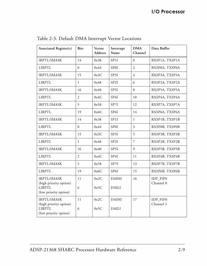
ADSP-21368 SHARC Processor Hardware Reference 2-9
I/O Processor
Table 2-3. Default DMA Interrupt Vector Locations
Associated Register(s) Bits Vector Address
Interrupt Name
DMA Channel
Data Buffer
IRPTL/IMASK 14 0x38 SP1I 0 RXSP1A, TXSP1A
LIRPTL 0 0x44 SP0I 2 RXSP0A, TXSP0A
IRPTL/IMASK 15 0x3C SP3I 4 RXSP3A, TXSP3A
LIRPTL 1 0x48 SP2I 6 RXSP2A, TXSP2A
IRPTL/IMASK 16 0x40 SP5I 8 RXSP5A, TXSP5A
LIRPTL 2 0x4C SP4I 10 RXSP4A, TXSP4A
IRPTL/IMASK 5 0x58 SP7I 12 RXSP7A, TXSP7A
LIRPTL 19 0x6C SP6I 14 RXSP6A, TXSP6A
IRPTL/IMASK 14 0x38 SP1I 1 RXSP1B, TXSP1B
LIRPTL 0 0x44 SP0I 3 RXSP0B, TXSP0B
IRPTL/IMASK 15 0x3C SP3I 5 RXSP3B, TXSP3B
LIRPTL 1 0x48 SP2I 7 RXSP2B, TXSP2B
IRPTL/IMASK 16 0x40 SP5I 9 RXSP5B, TXSP5B
LIRPTL 2 0x4C SP4I 11 RXSP4B, TXSP4B
IRPTL/IMASK 5 0x58 SP7I 13 RXSP7B, TXSP7B
LIRPTL 19 0x6C SP6I 15 RXSP6B, TXSP6B
IRPTL/IMASK (high priority option)LIRPTL (low priority option)
11
6
0x2C
0x5C
DAIHI
DAILI
16 IDP_FIF0Channel 0
IRPTL/IMASK (high priority option)LIRPTL (low priority option)
11
6
0x2C
0x5C
DAIHI
DAILI
17 IDP_FIF0Channel 1
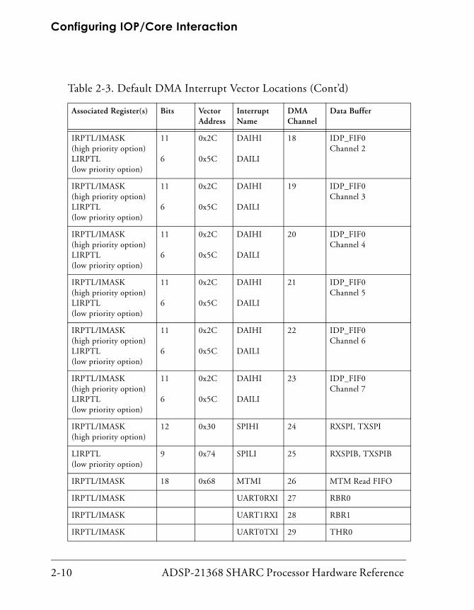
Configuring IOP/Core Interaction
2-10 ADSP-21368 SHARC Processor Hardware Reference
IRPTL/IMASK (high priority option)LIRPTL (low priority option)
11
6
0x2C
0x5C
DAIHI
DAILI
18 IDP_FIF0Channel 2
IRPTL/IMASK (high priority option)LIRPTL (low priority option)
11
6
0x2C
0x5C
DAIHI
DAILI
19 IDP_FIF0Channel 3
IRPTL/IMASK (high priority option)LIRPTL (low priority option)
11
6
0x2C
0x5C
DAIHI
DAILI
20 IDP_FIF0Channel 4
IRPTL/IMASK (high priority option)LIRPTL (low priority option)
11
6
0x2C
0x5C
DAIHI
DAILI
21 IDP_FIF0Channel 5
IRPTL/IMASK (high priority option)LIRPTL (low priority option)
11
6
0x2C
0x5C
DAIHI
DAILI
22 IDP_FIF0Channel 6
IRPTL/IMASK (high priority option)LIRPTL (low priority option)
11
6
0x2C
0x5C
DAIHI
DAILI
23 IDP_FIF0Channel 7
IRPTL/IMASK (high priority option)
12 0x30 SPIHI 24 RXSPI, TXSPI
LIRPTL (low priority option)
9 0x74 SPILI 25 RXSPIB, TXSPIB
IRPTL/IMASK 18 0x68 MTMI 26 MTM Read FIFO
IRPTL/IMASK UART0RXI 27 RBR0
IRPTL/IMASK UART1RXI 28 RBR1
IRPTL/IMASK UART0TXI 29 THR0
Table 2-3. Default DMA Interrupt Vector Locations (Cont’d)
Associated Register(s) Bits Vector Address
Interrupt Name
DMA Channel
Data Buffer

ADSP-21368 SHARC Processor Hardware Reference 2-11
I/O Processor
For more information, see the program sequencer “Interrupts and Sequencing” section of Chapter 3 in the ADSP-2136x SHARC Processor Programming Reference and Appendix B, Interrupts.
Interrupt Latency in Interrupt-Driven Transfers
During an interrupt-driven I/O transfer from any peripheral that uses an IOP interrupt service routine, a write into an IOP register to clear the interrupt causes a certain amount of latency. If the program comes out of the interrupt service routine during that period of latency, the interrupt is generated again.
To avoid the interrupt from being regenerated, use one of the following solutions.
1. Read an IOP register from the same peripheral block before the return from interrupt (RTI). The read forces the write to occur as shown in the example code below.
isr_code:
R0 = 0x0;
dm(SPICTL) = R0; /* disable SPI */
R0 = dm(SPICTL); /* dummy read, occurs only after
write */
rti;
IRPTL/IMASK UART1TXI 30 THR1
LIRPTL 0x50 EPDMA 31 EPDF0
LIRPTL EPDMA 32 EPTF0
LIRPTL 0x50 EPDMA 33 EPDF1
IRPTL/IMASK MTMI 34 MTM Write FIFO
Table 2-3. Default DMA Interrupt Vector Locations (Cont’d)
Associated Register(s) Bits Vector Address
Interrupt Name
DMA Channel
Data Buffer

Configuring IOP/Core Interaction
2-12 ADSP-21368 SHARC Processor Hardware Reference
2. Add sufficient NOP instructions after a write. In the worst case pro-grams need to add ten NOP instructions after a write as shown in the example code below.
isr_code: R0 = 0x0;
dm(SPICTL) = R0; /* disable SPI */
nop; nop; nop; nop; nop;
nop; nop; nop; nop; nop;
rti;
3. Read a status register from the same peripheral block to check whether the interrupt has cleared.
Polling/Status-Driven I/OThe second method of controlling I/O is through status polling. The I/O processor monitors the status of data transfers on DMA channels and indi-cates interrupt status in the IRPTL, LIRPTL, DAI_IRPTL_H, and DAI_IRPTL_L registers. Note that because polling uses processor resources it is not as efficient as an interrupt-driven system. Also note that polling the DMA status registers reduces I/O bandwidth. The following provide more infor-mation on the registers that control and monitor I/O processes.
• All the bits in the IRPTL and LIRPTL registers are shown in “Inter-rupt Latch Register (IRPTL)” on page B-13 and “Interrupt Register (LIRPTL)” on page B-6.
• Figure A-44 on page A-114 lists all the bits in the DAI_IRPTL_H and DAI_IRPTL_L registers.
The DMA controller in the ADSP-21367/8/9 and ADSP-2137x proces-sors maintains the status information of the channels in each of the peripherals registers, SPMCTLx, EPDMACTL, DAI_STAT, DPI_PIN_STAT, RXSTAT_UACx, TXSTAT_UACx and SPIDMAC. More information on these regis-ters can be found at the following locations.

ADSP-21368 SHARC Processor Hardware Reference 2-13
I/O Processor
• Bit definitions for the SPIDMAC register are illustrated in “SPI Port Status (SPISTAT, SPISTATB) Registers” on page A-56.
• Bit definitions for the SPMCTLx register are illustrated in “SPORT Multichannel Control Registers (SPMCTLx)” on page A-40.
• Bit definitions for the DAI_STAT register are illustrated in Figure A-41 on page A-110.
Note that there is a one-cycle latency between a change in DMA channel status and the status update in the corresponding register.
DMA Controller OperationThere are two methods you can use to start DMA sequences: chaining and non-chaining.
Non-chained DMA. To start a new DMA sequence after the current one is finished, a program must first clear the DMA enable bit, write new parameters to the index, modify, and count registers, then set the DMA enable bit to re-enable DMA.
Chained DMA. Chained DMA sequences are a set of multiple DMA operations, each autoinitializing the next in line. To start a new DMA sequence after the current one is finished, the IOP automatically loads new index, modify, and count values from an internal memory location pointed to by that channel’s chain pointer register. Using chaining, pro-grams can set up consecutive DMA operations and each operation can have different attributes.
Chaining is only supported on the SPI and SPORT DMA chan-nels. The IDP port does not support chaining.

Configuring IOP/Core Interaction
2-14 ADSP-21368 SHARC Processor Hardware Reference
In general, a DMA sequence starts when one of the following occurs:
• Chaining is disabled, and the DMA enable bit transitions from low to high.
• Chaining is enabled, DMA is enabled, and the chain pointer regis-ter address field is written with a nonzero value. In this case, TCB chain loading of the channel parameter registers occurs first.
• Chaining is enabled, the chain pointer register address field is non-zero, and the current DMA sequence finishes. Again, TCB chain loading occurs.
A DMA sequence ends when one of the following occurs:
• The count register decrements to zero, and the chain pointer regis-ter is zero.
• Chaining is disabled and the channel’s DMA enable bit transitions from high to low. If the DMA enable bit goes low (=0) and chain-ing is enabled, the channel enters chain insertion mode and the DMA sequence continues. For more information, see “Inserting a TCB in an Active Chain” on page 2-41.
Once a program starts a DMA process, the process is influenced by two external controls—DMA channel priority and DMA chaining. For more information, see “Managing DMA Channel Priority” on page 2-19 or “Chaining DMA Processes” below.
Chaining DMA Processes
The location of the DMA parameters for the next sequence comes from the chain pointer register. In chained DMA operations, the processor automatically initializes and then begins another DMA transfer when the current DMA transfer is complete. In addition to the standard DMA parameter registers, each DMA channel (SPORT, eternal port, UART and SPI) also has a chain pointer register that points to the next set of DMA

ADSP-21368 SHARC Processor Hardware Reference 2-15
I/O Processor
parameters stored in the processor’s internal memory. These are the CPSPxy registers for the SPORTs, the CPEP register for the external port, the RXCP_UACx registers for the UART, and the CPSPI register for the SPI. Each new set of parameters is stored in a four-word, user-initialized buffer in internal memory known as a transfer control block (TCB).
The structure of a TCB is conceptually the same as that of a traditional linked list. Each TCB has several data values and a pointer to the next TCB. Further, the chain pointer of a TCB may point to itself to con-stantly reiterate the same DMA.
A DMA sequence is defined as the sum of the DMA transfers for a single channel, from when the parameter registers initialize to when the count register decrements to zero. Each DMA channel has a chaining enable bit (CHEN) in the corresponding control register. This bit must be set to one to enable chaining. When chaining is enabled, DMA transfers are initiated by writing a memory address to the chain pointer register. This is also an easy way to start a single DMA sequence, with no subsequent chained DMAs.
The chain pointer register can be loaded at any time during the DMA sequence. This allows a DMA channel to have chaining disabled (chain pointer register address field = 0x0000) until some event occurs that loads the chain pointer register with a nonzero value. Writing all zeros to the address field of the chain pointer register also disables chaining.
If chaining is enabled on a DMA channel, programs should not use poll-ing to determine channel status as it can provide inaccurate information. In this case, the DMA appears inactive if it is sampled while the next transfer control block (TCB) is loading.
Chained DMA operations may only occur within the same chan-nel. The processor does not support cross-channel chaining.
The chain pointer register is 20 bits wide. The lower 19 bits are the mem-ory address field. Like other I/O processor address registers, the chain pointer register’s value is offset to match the starting address of the

Configuring IOP/Core Interaction
2-16 ADSP-21368 SHARC Processor Hardware Reference
processor’s internal memory before it is used by the I/O processor. On the ADSP-21367/8/9 and ADSP-2137x processors, this offset value is 0x0008 0000.
Bit 19 of the chain pointer register is the program-controlled interrupts (PCI) bit. This bit controls whether an interrupt is latched after every DMA in the chain (when set), or whether the interrupt is latched after the entire DMA sequence completes (if cleared).
The PCI bit only effects DMA channels that have chaining enabled. Also, interrupt requests enabled by the PCI bit are maskable with the IMASK register.
Because the PCI bit is not part of the memory address in the chain pointer register, programs must use care when writing and reading addresses to and from the register. To prevent errors, programs should mask out the PCI bit (bit 19) when copying the address in a chain pointer register to another address register.
The DMA registers are shown in Figure 2-1.
Transfer Control Block Chain Loading (TCB)
During TCB chain loading, the I/O processor loads the DMA channel parameter registers with values retrieved from internal memory. The address in the chain pointer register points to the highest address of the TCB (containing the index parameter). This means that if a program declares an array to hold the TCB, the chain pointer register should not point to the first location of the array.
Table 2-4 shows the TCB-to-register loading sequence for the serial port and SPI port DMA channels. The I/O processor reads each word of the TCB and loads it into the corresponding register. Programs must set up the TCB in memory in the order shown in Table 2-4, placing the index parameter at the address pointed to by the chain pointer register of the

ADSP-21368 SHARC Processor Hardware Reference 2-17
I/O Processor
previous DMA operation of the chain. The end of the chain (no further TCBs are loaded) is indicated by a TCB with a chain pointer register value of zero.
Figure 2-1. DMA Parameter Registers
PCI Bit
31 30 29 28 27 26 25 24 23 22 21 20 19 18 17 16 15 14 13 12 11 10 9 8 7 6 5 4 3 2 1 0
CPx
31 30 29 28 27 26 25 24 23 22 21 20 19 18 17 16 15 14 13 12 11 10 9 8 7 6 5 4 3 2 1 0
EIPP
31 30 29 28 27 26 25 24 23 22 21 20 19 18 17 16 15 14 13 12 11 10 9 8 7 6 5 4 3 2 1 0
31 30 29 28 27 26 25 24 23 22 21 20 19 18 17 16 15 14 13 12 11 10 9 8 7 6 5 4 3 2 1 0
EMPP
ECPP
Program – Controlled Interrupt BitIf this bit is set, the I/O processor generates aDMA interrupt after every DMA in the chain.
31 30 29 28 27 26 25 24 23 22 21 20 19 18 17 16 15 14 13 12 11 10 9 8 7 6 5 4 3 2 1 0
IIx
31 30 29 28 27 26 25 24 23 22 21 20 19 18 17 16 15 14 13 12 11 10 9 8 7 6 5 4 3 2 1 0
31 30 29 28 27 26 25 24 23 22 21 20 19 18 17 16 15 14 13 12 11 10 9 8 7 6 5 4 3 2 1 0
IMx
Cx

Configuring IOP/Core Interaction
2-18 ADSP-21368 SHARC Processor Hardware Reference
A TCB chain load request is prioritized like all other DMA operations. The I/O processor latches a TCB loading request and holds it until the load request has the highest priority. If multiple chaining requests are present, the I/O processor services the TCB registers for the highest priority DMA channel first. A channel that is in the process of chain loading can-not be interrupted by a higher priority channel. For a list of DMA channels in priority order, see Table 2-7 on page 2-32.
Setting Up DMA Channel Allocation and PrioritiesThere are between 24 and 34 channels of DMA available on the ADSP-21367/8/9 and ADSP-2137x processors, depending on the proces-sor model. The maximum number is configured as—16 via the serial ports, 8 via the input data port, 4 for the UARTs, 2 for the SPI interface, 2 for the external port, and 2 for memory-to-memory transfers. Each channel has a set of parameter registers which are used to set up DMA
Table 2-4. TCB Chain Loading Sequence1
Address2 External Port Serial Ports SPI Port
CPSPx + 0x0008 0000 See Table 2-9, Table 2-10, Table 2-11
IISPx IISPI
CPSPx – 1 + 0x0008 0000 IMSPx IMSPI
CPSPx – 2 + 0x0008 0000 CSPx CSPI
CPSPx – 3 + 0x0008 0000 CPSPx CPSPI
CPSPx – 4 + 0x0008 0000
CPSPx – 5 + 0x0008 0000
CPSPx – 6 + 0x0008 0000
1 Chaining is not available using the IDP port.2 An “x” denotes the DMA channel used. While the TCB is eight locations in length, SPI and serial
ports only use the first four locations.

ADSP-21368 SHARC Processor Hardware Reference 2-19
I/O Processor
transfers. Table 2-5 shows the DMA channel allocation and parameter register assignments for the ADSP-21367/8/9 and ADSP-2137x processors.
DMA channels vary by processor model. For a breakdown of DMA channels for a particular model, see the processor specific data sheet.
Managing DMA Channel Priority
The DMA channel prioritization scheme ranks channel 0 as highest prior-ity and channel 34 as the lowest priority. Table 2-7 on page 2-32 lists the DMA channels in priority order. When a channel becomes the highest priority requester, the I/O processor services the channel’s request. In the next clock cycle, the I/O processor starts the DMA transfer.
The I/O data (IOD) bus is 32 bits wide and is the only path that the IOP uses to transfer data between internal memory and the peripherals. When there are two or more peripherals with active DMAs in progress, they may all require data to be moved to or from memory in the same cycle. For example, the input data port may fill its RXPP buffer just as a SPORT shifts a word into its RXn buffer. To determine which word is transferred first, the DMA channels for each of the processor’s I/O ports negotiate channel priority with the I/O processor using an internal DMA request/grant handshake.
Each I/O port has one or more DMA channels, and each channel has a single request and a single grant. When a particular channel needs to read or write data to internal memory, the channel asserts an internal DMA request. The I/O processor prioritizes the request with all other valid DMA requests. When a channel becomes the highest priority requester, the I/O processor asserts the channel’s internal DMA grant. In the next clock cycle, the DMA transfer starts. Figure 2-3 on page 2-30 shows the paths for internal DMA requests within the I/O processor.

Configuring IOP/Core Interaction
2-20 ADSP-21368 SHARC Processor Hardware Reference
If a DMA channel is disabled (EPDEN, SPIDEN, SDEN, or IDP_DMA_EN bits =0), the I/O processor does not issue internal DMA grants to that channel (whether or not the channel has data to transfer).
The default DMA channel priority is fixed prioritization by DMA channel group (serial ports, TWI, UART, IDP, or SPI port). Table 2-7 on page 2-32 lists the DMA channels in descending order of priority.
For information on programming serial port priority modes, see Table 5-11 on page 5-74.
The I/O processor determines which DMA channel has the highest prior-ity internal DMA request during every cycle between each data transfer.
Processor core accesses of I/O processor registers and TCB chain loading (both of which occur after the IOD transfer) are subject to the same prior-itization scheme as the DMA channels. Applying this scheme uniformly prevents I/O bus contention, because these accesses are also performed over the internal I/O bus. For more information, see “Chaining DMA Processes” on page 2-14.
DMA Bus Arbitration
DMA channel arbitration is the method that the IOP uses to determine how groups rotate priority with other channels. This feature is enabled by setting the DCPR bit in the IOP’s SYSCTL register.
DMA-capable peripherals execute DMA data transfers to and from inter-nal memory over the IOD bus. When more than one of these peripherals requests access to the IOD bus in a clock cycle, the bus arbiter, which is attached to the IOD bus, determines which master should have access to the bus and grants the bus to that master.
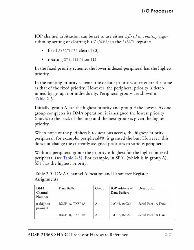
ADSP-21368 SHARC Processor Hardware Reference 2-21
I/O Processor
IOP channel arbitration can be set to use either a fixed or rotating algo-rithm by setting or clearing bit 7 (DCPR) in the SYSCTL register:
• fixed SYSCTL[7] cleared (0)
• rotating SYSCTL[7] set (1)
In the fixed priority scheme, the lower indexed peripheral has the highest priority.
In the rotating priority scheme, the default priorities at reset are the same as that of the fixed priority. However, the peripheral priority is deter-mined by group, not individually. Peripheral groups are shown in Table 2-5.
Initially, group A has the highest priority and group F the lowest. As one group completes its DMA operation, it is assigned the lowest priority (moves to the back of the line) and the next group is given the highest priority.
When none of the peripherals request bus access, the highest priority peripheral, for example, peripheral#0, is granted the bus. However, this does not change the currently assigned priorities to various peripherals.
Within a peripheral group the priority is highest for the higher indexed peripheral (see Table 2-5). For example, in SP01 (which is in group A), SP1 has the highest priority.
Table 2-5. DMA Channel Allocation and Parameter Register Assignments
DMA Channel Number
Data Buffer Group IOP Address of Data Buffers
Description
0 (highest priority)
RXSP1A, TXSP1A A 0xC65, 0xC64 Serial Port 1A Data
1 RXSP1B, TXSP1B A 0xC67, 0xC66 Serial Port 1B Data

Configuring IOP/Core Interaction
2-22 ADSP-21368 SHARC Processor Hardware Reference
2 RXSP0A, TXSP0A A 0xC61, 0xC60 Serial Port 0A Data
3 RXSP0B, TXSP0B A 0xC63, 0xC62 Serial Port 0B Data
4 RXSP3A, TXSP3A B 0x465, 0x464 Serial Port 3A Data
5 RXSP3B, TXSP3B B 0x467, 0x466 Serial Port 3B Data
6 RXSP2A, TXSP2A B 0x461, 0x460 Serial Port 2A Data
7 RXSP2B, TXSP2B B 0x463, 0x462 Serial Port 2B Data
8 RXSP5A, TXSP5A C 0x865, 0x864 Serial Port 5A Data
9 RXSP5B, TXSP5B C 0x867, 0x866 Serial Port 5B Data
10 RXSP4A, TXSP4A C 0x861, 0x860 Serial Port 4A Data
11 RXSP4B, TXSP4B C 0x863, 0x862 Serial Port 4B Data
12 RXSP7A, TXSP7A C 0x04865, 0x04864
Serial Port 7A Data
13 RXSP7B, TXSP7B C 0x04867, 0x04866
Serial Port 7B Data
14 RXSP6A, TXSP6A C 0x04861 or 0x04860
Serial Port 6A Data
15 RXSP6B, TXSP6B C 0x04863 or 0x04862
Serial Port 6B Data
16 IDP_FIF0 D 0x24D0 DAI IDP Channel 0
17 IDP_FIF0 D 0x24D0 DAI IDP Channel 1
18 IDP_FIF0 D 0x24D0 DAI IDP Channel 2
19 IDP_FIF0 D 0x24D0 DAI IDP Channel 3
20 IDP_FIF0 D 0x24D0 DAI IPD Channel 4
21 IDP_FIF0 D 0x24D0 DAI IDP Channel 5
Table 2-5. DMA Channel Allocation and Parameter Register Assignments (Cont’d)
DMA Channel Number
Data Buffer Group IOP Address of Data Buffers
Description

ADSP-21368 SHARC Processor Hardware Reference 2-23
I/O Processor
22 IDP_FIF0 D 0x24D0 DAI IDP Channel 6
23 IDP_FIF0 D 0x24D0 DAI IDP Channel 7
24 RXSPI, TXSPI E 0x1004, 0x1003 SPI Data
25 RXSPIB, TXSPIB G 0x2804, 0x2803 SPI Data
26 MTM Read FIFO G Not accessible Memory-to-Memory Read Data
27 THR0 G 0x3C00 UART0 Transmit Holding Register
28 RBR0 G 0x3C00 UART0 Receive Buffer Register
29 THR1 G 0x4000 UART1 Transmit Holding Register
30 RBR1 G 0x4000 UART1 Receive Buffer Register
31 EPDF0 G 0x182C External Port Channel0 Data FIFO
32 EPTF0 G 0x182D External Port Channel0 Tap List FIFO
33 EPDF1 G 0x183C External Port Channel1 Data FIFO
34 EPTF1 G 0x183D External Port Channel1 Tap List FIFO
35 (lowest priority)
MTM Write FIFO G Not accessible Memory-to Memory Write Data
Table 2-5. DMA Channel Allocation and Parameter Register Assignments (Cont’d)
DMA Channel Number
Data Buffer Group IOP Address of Data Buffers
Description
Setting Up DMA Parameter Registers
2-24 ADSP-21368 SHARC Processor Hardware Reference
Setting Up DMA Parameter RegistersOnce you have determined and configured the DMA options, you can configure the DMA parameter registers. The parameter registers control the source and destination of the data, the size of the data buffer, and the step size used. These topics are described in detail in the following sections.
DMA Transfer DirectionDMA transfers between internal memory and external memory devices use the processor’s external port. For these types of transfers, a program pro-vides the DMA controller with the internal memory buffer size, address, and address modifier, as well as the external memory buffer size, address and address modifier and the direction of transfer. After setup, the DMA transfers begin when the program enables the channel and continues until the I/O processor transfers the entire buffer to processor memory. Table 2-6 on page 2-29 shows the parameter registers for each DMA channel.
Similarly, DMA transfers between internal memory and serial, IDP or SPI ports have DMA parameters. When the I/O processor performs DMA between internal memory and one of these ports, the program sets up the parameters, and the I/O uses the port instead of the external bus.
Additionally, the ADSP-21367/8/9 and ADSP-2137x processors can use DMA to transfer 64-bit blocks of data between internal memory locations.
The direction (receive or transmit) of the peripheral determines the direc-tion of data transfer. When the port receives data, the I/O processor automatically transfers the data to internal memory. When the port needs to transmit a word, the I/O processor automatically fetches the data from internal memory. Figure 2-2 shows the processor’s I/O processor, related ports, and buses. Figure 2-3 on page 2-30 shows more detail on DMA channel data paths.

ADSP-21368 SHARC Processor Hardware Reference 2-25
I/O Processor
Data Buffer RegistersFigure 2-2 shows the data buffer registers for each port. These registers include:
• Serial port receive buffers (RXSPx). These receive buffers for the serial ports have two-position FIFOs for receiving data when con-nected to another serial device.
Figure 2-2. I/O Processor Block Diagram
ID P
ID P F IFO8 D E E P
E X TE R N E LP O R T
EX TE R N A LA D D R E SS
G EN E R A TO R
TX SP 5A -0A ,TX SP 5B -0B ,R X S P5A -0A ,R X SP 5B -0B
(2 D E E P)
SP O R T S
SP I P O R T
R X S P I, T XS P I(1 D EE P EA C H )
S PID M AFIFO
(4 D EE P )
IO D B U S
IIS PI, IM S PI,C S P I, C P S PI
S PI
IIS P7A -0A ,IIS P7B -0B ,
IM SP 7A -0A ,IM S P 7B -0BC S P7A -0A ,C S P7B -0B ,
C PS P 7A -0A ,C P SP 7B -0B
S P O R T
IO A B U S
IN T ER N A LD M A
P R IO R IT IZE R
D M D , P M DB U S ES (T O C O R E)
I/O P R O C E S S O R
ID P _D M A _IxID P _D M A _M xID P _D M A _C x
ID P
M U X M U X
U A R T
U A R T xR XC T L , IIU A R TxR XIM U A R TxR X, C U A R TxR X
C PU A R T xR X, U A R T xR XS TA TU A R TxT XC T L , IIU A R TxTXIM U A R T xT X, C U A R TxTX
C P U A R TxT X, U A R T xTXS TA T
E XT ER N A LPO R T
E IEP x , E M E P xE C E P x, IIE P xIM E Px , IC E P xC E P x , C PE P x
E B E Px , T PE P xE LE P x
D F EP 0 (D A TA F IFO )TFE P 0 (TA P L IS T FIFO )

Setting Up DMA Parameter Registers
2-26 ADSP-21368 SHARC Processor Hardware Reference
• Serial port transmit buffers (TXSPx). These transmit buffers for the serial ports have two-position FIFOs for transmitting data when connected to another serial device.
• SPI receive buffers (RXSPI, RXSPIB). These receive buffers for the SPI ports have a single-position buffer for receiving data when con-nected to another serial device.
• SPI transmit buffers (TXSPI, TXSPIB). These transmit buffers for the SPI ports have a single-position buffer for transmitting data when connected to another serial device.
• Input data port buffers (IDP_FIFO). This receive buffer for the input data port has eight-position buffers for receiving data when connected to another device.
Port, Buffer, and DMA Control RegistersThe port, buffer, and DMA control registers in Figure 2-2 shows the con-trol registers for the ports and DMA channels. These registers include:
• External port control registers (DMACx). These are the control regis-ters for the external port DMA channels.
• Input data port control register (IDP_CTL). This is the control reg-ister for the input data ports.
• Serial port control registers (SPCTLx, SPMCTLx). These control reg-isters select the receive or transmit format, monitor FIFO status, enable chaining, and start DMA for each serial port.
• SPI port control registers (SPICTL, SPICTLB). These control regis-ters configure and enable the two SPI interfaces, selecting the devices as masters or slaves, and determine the data transfer and word size. The SPIDMAC and SPIDMACB registers also control SPI DMA and FIFO status.
ADSP-21368 SHARC Processor Hardware Reference 2-27
I/O Processor
• Universal asynchronous receiver/transmitter registers (RXCTL_UACx, TXCTL_UACx). These control registers configure and enable the UART receiver and transmitter DMA, (chaining and non chaining).
• Memory-to-memory DMA control register (MTMCTL). This control register contains the MTM DMA read and write channel enable and status bits.
Table 2-6 shows the parameter registers for each DMA channel. These registers function similarly to data address generator registers and include:
• Internal index registers (IISPx, IISPI, IISPIB, IIEP, IDP_DMA_Ix, RXI_UAC/TXI_UAC). Index registers provide an internal memory address, acting as a pointer to the next internal memory DMA read or write location.
• Internal modify registers (IMSPx, IMEP, IMSPI, IMSPIB, IDP_DMA_Mx, RXM_UAC/TXM_UAC). Modify registers provide the signed increment by which the DMA controller post-modifies the corresponding internal memory index register after the DMA read or write.
• Count registers (CSPx, ICEP, CSPI, CSPIB, IDP_DMA_Cx, RXC_UAC/TXC_UAC). Count registers indicate the number of words remaining to be transferred to or from internal memory on the cor-responding DMA channel.
• Chain pointer registers (CPSPx, CPSPI, CPSPIB, CPEP, RXCP_UAC/TXCP_UAC). Chain pointer registers hold the starting address of the TCB (parameter register values) for the next DMA operation on the corresponding channel. These registers also con-trol whether the I/O processor generates an interrupt when the current DMA process ends.
• External index registers (EIEPx). Index registers provide an exter-nal memory address, acting as a pointer to the next external memory DMA read or write location.

Setting Up DMA Parameter Registers
2-28 ADSP-21368 SHARC Processor Hardware Reference
• External modify registers (EMEPx). Modify registers provide the increment by which the DMA controller post-modifies the corre-sponding external memory index register after the DMA read or write.
• External count registers (ECEPx). External count registers indicate the number of words remaining to be transferred to or from exter-nal memory on the corresponding DMA channel.
• Memory-to-memory write index register (IIMTMW). This register provides the base address in memory where DMA writes start.
• Memory-to-memory write modify register (IMMTMW). The MTM modify register modifies the write index register after each 32-bit write.
• Memory-to-memory write counter register (CMTMW). The MTM counter register indicates the quantity of 32-bit data to be trans-ferred to memory. The counter is decremented by one after each data write.
• Memory-to-memory read index register (IIMTMR). This register provides the base address in memory where DMA reads start.
• Memory-to-memory read modify register (IMMTMR). The MTM modify register modifies the write index register after each 32-bit read.
• Memory-to-memory read counter register (CMTMR). The MTM counter register indicates the quantity of 32-bit data to be read from memory. The counter is decremented by one after each data write.

ADSP-21368 SHARC Processor Hardware Reference 2-29
I/O Processor
AddressingFigure 2-3 shows a block diagram of the I/O processor’s address generator (DMA controller). Table 2-6 lists the parameter registers for each DMA channel. The parameter registers are uninitialized following a processor reset.
The I/O processor generates addresses for DMA channels much the same way that the data address generators (DAGs) generate addresses for data memory accesses. Each channel has a set of parameter registers including an index register and modify register that the I/O processor uses to address a data buffer in internal memory. The index register must be initialized with a starting address for the data buffer. As part of the DMA operation, the I/O processor outputs the address in the index register onto the pro-cessor’s I/O address bus and applies the address to internal memory during each DMA cycle—a clock cycle in which a DMA transfer is taking place.
Table 2-6. DMA Parameter Registers
Register Function Width Description
IIy Internal Index Register 19 bits Address of buffer in internalmemory
IMxy Internal Modify Register 16 bits1 Stride for internal buffer
Cxy Internal Count Register 16 bits Length of internal buffer
CPxy Chain Pointer Register 20 bits Chain pointer for DMA chaining
EIEP External Index Register 19 bits Address of buffer in externalmemory
EMEP External Modify Register 16 bits Stride for external buffer
ECEP External Count Register 16 bits Length of external buffer
1 IDP_DMA_Mx registers are 6 bits wide only.

Setting Up DMA Parameter Registers
2-30 ADSP-21368 SHARC Processor Hardware Reference
All addresses in the index registers are offset by a value that matches the processor’s first internal normal word addressed RAM location (before the I/O processor uses the addresses). For the ADSP-21367/8/9 and ADSP-2137x processors, this offset value is 0x0008 0000.
Figure 2-3. DMA Address Generator
LOCAL BUS
IMXMODIFIER
INTERNALMEMORYADDRESS
DMA ADDRESS GENERATOR (INTERNAL ADDRESSES)
LOCAL BUS
CXCOUNT
CPXCHAIN POINTER
MUX
DMA WORD COUNTER
– 1
WORKING REGISTER
IIXINDEX (ADDRESS)
+/-POST-MODIFY
+
LOCAL BUS
EMPPEXT. MODIFIER
ECPPEXT. COUNT
– 1
EXTERNALMEMORYADDRESS
POST-MODIFY
EIPPEXT. INDEX (ADDRESS)
DMA ADDRESS GENERATOR (EXTERNAL ADDRESSES)
++

ADSP-21368 SHARC Processor Hardware Reference 2-31
I/O Processor
The following rules for data transfers must be followed.
• DMA addresses must always be normal word (32-bit) memory.
• Internal memory data transfer sizes are 32 bits, while external data transfer sizes may be 32, 16, or 8 bits.
• The I/O processor can transfer short word data (16-bit) using the packing capability of the serial port and SPI port DMA channels.
After transferring each data word to or from internal memory, the I/O processor adds the modify value to the index register to generate the address for the next DMA transfer and writes the modified index value to the index register. The modify value in the modify register is a signed inte-ger, which allows both increment and decrement modifies. The modify value can have any positive or negative integer value. Note that:
• If the I/O processor modifies the index register past the maximum 18-bit value to indicate an address out of internal memory, the index wraps around to zero. With the offset for the ADSP-2136x SHARC processor processors, the wraparound address is 0x0008 0000.
• If a DMA channel is disabled, the I/O processor does not service requests for that channel, (whether or not the channel has data to transfer).
If a program loads the count register with zero, the I/O processor does not disable DMA transfers on that channel. The I/O proces-sor interprets the zero as a request for 216 transfers. This count occurs because the I/O processor starts the first transfer before test-ing the count value. The only way to disable a DMA channel is to clear its DMA enable bit.
The processor’s 34 DMA channels are numbered as shown in Table 2-7. This table also shows the control, parameter, and data buffer registers that correspond to each channel.

Setting Up DMA Parameter Registers
2-32 ADSP-21368 SHARC Processor Hardware Reference
In the serial port pair SP0/1, SP1 has a higher priority. For multichannel pairs, the odd numbered channels have a higher priority (for example SP3, SP5).
Table 2-7. DMA Channel Registers: Controls, Parameters, and Buffers
DMA Channel Number
Control Registers Parameter Registers Buffer Registers Description
0 SPCTL1 IISP1A, IMSP1A, CSP1A, CPSP1A
RXSP1A, TXSP1A
Serial Port 1A Data
1 SPCTL1 IISP1B, IMSP1B, CSP1B, CPSP1B
RXSP1B, TXSP1B
Serial Port 1B Data
2 SPCTL0 IISP0A, IMSP0A, CSP0A, CPSP0A
RXSP0A, TXSP0A
Serial Port 0A Data
3 SPCTL0 IISP0B, IMSP0B, CSP0B, CPSP0B
RXSP0B, TXSP0B
Serial Port 0B Data
4 SPCTL3 IISP3A, IMSP3A, CSP3A, CPSP3A
RXSP3A, TXSP3A
Serial Port 3A Data
5 SPCTL3 IISP3B, IMSP3B, CSP3B, CPSP3B
RXSP3B, TXSP3B
Serial Port 3B Data
6 SPCTL2 IISP2A, IMSP2A, CSP2A, CPSP2A
RXSP2A, TXSP2A
Serial Port 2A Data
7 SPCTL2 IISP2B, IMSP2B, CSP2B, CPSP2B
RXSP2B, TXSP2B
Serial Port 2B Data
8 SPCTL5 IISP5A, IMSP5A, CSP5A, CPSP5A
RXSP5A, TXSP5A
Serial Port 5A Data
9 SPCTL5 IISP5B, IMSP5B, CSP5B, CPSP5B
RXSP5B, TXSP5B
Serial Port 5B Data
10 SPCTL4 IISP4A, IMSP4A, CSP4A, CPSP4A
RXSP4A, TXSP4A
Serial Port 4A Data
11 SPCTL4 IISP4B, IMSP4B, CSP4B, CPSP4B
RXSP4B, TXSP4B
Serial Port 4B Data

ADSP-21368 SHARC Processor Hardware Reference 2-33
I/O Processor
12 SPCTL7 IISP7A, IM7P5A, CSP7A, CPSP7A
RXSP7A, TXSP7A
Serial Port 7A Data
13 SPCTL7 IISP7B, IMSP7B, CSP7B, CPSP7B
RXSP7B, TXSP7B
Serial Port 7B Data
14 SPCTL6 IISP6A, IMSP6A, CSP6A, CPSP6A
RXSP6A, TXSP6A
Serial Port 6A Data
15 SPCTL6 IISP6B, IMSP6B, CSP6B, CPSP6B
RXSP6B, TXSP6B
Serial Port 6B Data
16 IDP_CTL IDP_DMA_I0, IDP_DMA_M0, IDP_DMA_C0
IDP_FIFO DAI IDP Channel 0
17 IDP_CTL IDP_DMA_I1, IDP_DMA_M1, IDP_DMA_C1
IDP_FIFO DAI IDP Channel 1
18 IDP_CTL IDP_DMA_I2, IDP_DMA_M2, IDP_DMA_C2
IDP_FIFO DAI IDP Channel 2
19 IDP_CTL IDP_DMA_I3, IDP_DMA_M3, IDP_DMA_C3
IDP_FIFO DAI IDP Channel 3
20 IDP_CTL IDP_DMA_I4, IDP_DMA_M4, IDP_DMA_C4
IDP_FIFO DAI IDP Channel 4
21 IDP_CTL IDP_DMA_I5, IDP_DMA_M5, IDP_DMA_C5
IDP_FIFO DAI IDP Channel 5
22 IDP_CTL IDP_DMA_I6, IDP_DMA_M6, IDP_DMA_C6
IDP_FIFO DAI IDP Channel 6
Table 2-7. DMA Channel Registers: Controls, Parameters, and Buffers (Cont’d)
DMA Channel Number
Control Registers Parameter Registers Buffer Registers Description

Setting Up DMA Parameter Registers
2-34 ADSP-21368 SHARC Processor Hardware Reference
23 IDP_CTL IDP_DMA_I7, IDP_DMA_M7, IDP_DMA_C7
IDP_FIFO DAI IDP Channel 7
24 SPICTL IISPI, IMSPI, CSPI, CPSPI RXSPI, TXSPI SPI Data
25 SPICTLB IISPIB, IMSPIB, CSPIB, CPSPIB
RXSPIB, TXSPIB
SPI B Data
26 MTMCTL IIMTMWIMMTMW,CMTMW
N/A MTM Write Channel
27 MTMCTL IIMTMR,IMMTMR,CMTMR
N/A MTM Read Channel
28 AMICTL EIEP0, EMEP0, ECEP0, IIEP0, IMEP0, ICEP0, CEP0, CPEP0, EBEP0, TPEP0, ELEP0
DFEP0, TFEP0 External Port Channel 0
29 AMICTL EIEP1, EMEP1, ECEP1, IIEP1, IMEP1, ICEP1, CEP1, CPEP1, EBEP1, TPEP1, ELEP1
DFEP1, TFEP1 External Port Channel 1
30 RXCTL_UAC0 RXI_UAC0, RXM_UAC0, RXC_UAC0, RXCP_UAC0, RXSTAT_UAC0
RBR0, RBRSH_UAC0
UART0 Rx
31 RXCTL_UAC1 RXI_UAC1, RXM_UAC1, RXC_UAC1, RXCP_UAC1, RXSTAT_UAC1
RBR1, RBRSH_UAC1
UART1 Rx
Table 2-7. DMA Channel Registers: Controls, Parameters, and Buffers (Cont’d)
DMA Channel Number
Control Registers Parameter Registers Buffer Registers Description

ADSP-21368 SHARC Processor Hardware Reference 2-35
I/O Processor
All of the I/O processor’s registers are memory-mapped, ranging from address 0x0000 0000 to 0x0003 FFFF. For more information on these registers, see “I/O Processor Registers” on page A-2.
External Port DMAThe external port has two DMA channels that can use either the SDRAM controller (SDC) or the asynchronous memory interface (AMI). The DMA chooses the correct interface (AMI or SDC) based on the external address as determined by bits 0–3 in the external port global control regis-ter (EPCTL, Table A-3 on page A-11). The DMA controllers support conventional DMA, chained and circular DMA, and delay line DMA. The priority of the two DMA channels is fixed with external port 0 having pri-ority over external port 1.
The DMA controllers have two FIFOs, a four deep data FIFO for received/transmitted data and a four deep tap list FIFO for the tap list entries for the delay line DMA.
The registers that control external port DMA are described in Table 2-8.
32 TXCTL_UAC0 TXI_UAC0, TXM_UAC0, TXC_UAC0, TXCP_UAC0, TXSTAT_UAC0
THR0 UART0 Tx
33 TXCTL_UAC1 TXI_UAC1, TXM_UAC1, TXC_UAC1, TXCP_UAC1, TXSTAT_UAC1
THR1 UART1 Tx
Table 2-7. DMA Channel Registers: Controls, Parameters, and Buffers (Cont’d)
DMA Channel Number
Control Registers Parameter Registers Buffer Registers Description

External Port DMA
2-36 ADSP-21368 SHARC Processor Hardware Reference
Setting Up and Starting Chained DMAUse the following procedure to set up and run a chained DMA on the external port.
1. Configure the AMICTLx registers to enable the AMI, set the desired wait states, set the data bus width, and so on. Configure the SDCTL register to enable the SDRAM, set the desired clock and timing set-tings, set the data bus width, and so on.
2. Initialize the CPEP register—set the PCI bit if interrupts are needed after the end of each DMA block.
Table 2-8. External Port Registers
Register Description Address
EPCTL External Port Global Control Register 0x1801
DMAC1–0 External Port DMA Control Register 0x180B, 0x180C
IIEP1–0 Internal Index Register 0x1823, 0x1833
IMEP1–0 Internal Modifier Register 0x1824, 0x1834
ICEP1–0 Internal Count Register 0x1825, 0x1835
EIEP1–0 External Index Register 0x1820, 0x1830
EMEP1–0 External Modifier Register 0x1821, 0x1831
CPEP1–0 Chain Pointer Register 0x1826, 0x1836
TPEP1–0 Tap List Pointer Register 0x1828, 0x1838
ELEP1–0 Circular Buffer Length Register 0x1829, 0x1839
EBEP1–0 External Base Address Register 0x1827, 0x1837

ADSP-21368 SHARC Processor Hardware Reference 2-37
I/O Processor
3. If circular buffering is needed, then program additional writes to the ELEP and EBEP registers. Note that for normal chained DMA, the ELEP and EBEP registers are not part of the TCB. So if circular buffering is used with the normal chained DMA, all the DMA blocks will have same ELEP and EBEP values.l
4. Enable DMA (DEN), chaining (CHEN), and circular buffering (CBEN) if needed, in the DMACx registers. It is advised that the DMA FIFOs are flushed (DFLSH) when DMA is enabled.
Once the DMA control register is initialized, the DMA controller fetches the DMA descriptors from the address pointed to by the external port chain pointer register (CPEP). The order the descriptors are fetched is shown in Table 2-9.
The order the descriptors are fetched with circular buffering enabled is shown in Table 2-10
Table 2-9. Chain Pointer Loading Sequence (Normal DMA)
Address Register Value
CPEP[18:0] IIEP
CPEP[18:0] – 0x1 IMEP
CPEP[18:0] – 0x2 ICEP
CPEP[18:0] – 0x3 EIEP
CPEP[18:0] – 0x4 EMEP
CPEP[18:0] – 0x5 CPEP

External Port DMA
2-38 ADSP-21368 SHARC Processor Hardware Reference
Once the DMA descriptors are fetched, the normal DMA process starts. Upon completion, new DMA descriptors are loaded and the process is repeated until CPEP = 0x00000. A DMA completion interrupt is generated at the end of each DMA block or at the end of an entire chained DMA, depending on the PCI bit setting.
Delay Line DMADelay line DMA is used to support reads and writes to external delay line buffers with limited core interaction. In this sense, delay line DMA is basi-cally a quantity of integrated writes followed by reads from external memory—called a delay line DMA access. The delay line DMA access con-sists of the following accesses in the order listed.
1. Writes to external memory. The number of writes are determined by the external port internal count ICEP register. The data is fetched from the external port internal index register (IIEP) and the external port internal modify register (IMEP) is used as the inter-nal modifier. The external port external index register (EIEP) serves
Table 2-10. Chain Pointer Loading Sequence (Circular Buffering Enabled)
Address Register Value
ELEP[18:0] IIEP
CPEP[18:0] – 0x1 IMEP
CPEP[18:0] – 0x2 ICEP
CPEP[18:0] – 0x3 EIEP
CPEP[18:0] – 0x4 EMEP
CPEP[18:0] – 0x5 CPEP
EPCP[18:0] – 0x5 EPEB
EPCP[18:0] – 0x6 EPEL
ADSP-21368 SHARC Processor Hardware Reference 2-39
I/O Processor
as the external index and is incremented by the external modifier register (EMEP) after each write. These writes are circular buffered if circular buffering is enabled.
2. In chained DMA, when the writes are complete, (ICEP = zero) the EPEI register, which serves as the write pointer of the delay line, is written back to the internal memory location from where it was fetched.
3. Reads from external memory. For reads, the tap list (TL) modifiers are used and the number of reads is determined by the external port read count register (RCEP). The write pointer in the external port external index register (EIEP) serves as the index address for these reads (reads start from where writes end). The EIEP register, along with tap list modifiers, are used in a pre-modify addressing mode to create the external address for the writes. For each 32-bit read the external index is:
• EIEP – TL[0] is the first read address (where TL[0] is the first tap list entry in internal memory as pointed to by the external port tap list pointer register TPEP).
• EIEP – TL[1] is the second address, and so on.
Therefore, for each read, the DMA controller fetches the external modifier from the tap list and the reads are circular buffered (if enabled).
The external address generation follows pre-modify addressing for reads in delay line DMA and therefore EIEP values are not modi-fied. Also the EMEP register does not have any effect during delay line reads.

Serial Port DMA
2-40 ADSP-21368 SHARC Processor Hardware Reference
4. Once the read count completes, the delay line DMA access is com-plete and the DMA complete interrupt is generated. Note that if chaining is enabled, the interrupt is generated based on the PCI bit setting. For more information on the PCI bit, see “Interrupt-Driven I/O” on page 2-6.
Serial Port DMAThe serial ports support standard as well as chained DMA.
Setting Up and Starting Chained DMATo set up and initiate a chain of DMA operations, use these steps:
1. Set up all TCBs in internal memory.
Table 2-11. Chain Pointer Loading Sequence (Delay Line DMA)
Address Register Value
EPCP[18:0] EPII (Write Index)
EPCP[18:0] – 0x1 EPIM
EPCP[18:0] – 0x2 EPIC (Write Count)
EPCP[18:0] – 0x3 EPEI
EPCP[18:0] – 0x4 EPEM
EPCP[18:0] – 0x5 EPEB
EPCP[18:0] – 0x6 EPEL
EPCP[18:0] – 0x7 EPRI
EPCP[18:0] – 0x8 EPRC
EPCP[18:0] – 0x9 EPTP
EPCP[18:0] – 0xA EPCP
ADSP-21368 SHARC Processor Hardware Reference 2-41
I/O Processor
2. Write to the appropriate DMA control register, setting the DMA enable bit to one and the chaining enable bit to one.
3. Write the address containing the index register value of the first TCB to the chain pointer register, which starts the chain.
The I/O processor responds by autoinitializing the first DMA parameter registers with the values from the first TCB, and then starts the first data transfer.
Inserting a TCB in an Active ChainIt is possible to insert a single DMA operation or another DMA chain within an active DMA chain. Programs may need to perform insertion when a high priority DMA requires service and cannot wait for the cur-rent chain to finish.
When DMA on a channel is disabled and chaining on the channel is enabled, the DMA channel is in chain insertion mode. This mode lets a program insert a new DMA or DMA chain within the current chain with-out effecting the current DMA transfer. Use the following sequence to insert a DMA subchain for the serial port 0A channel while another chain is active:
1. Enter chain insertion mode by setting SCHEN_A = 1 and SDEN_A = 0 in the channel’s DMA control register, SPCTL0. The DMA inter-rupt indicates when the current DMA sequence is complete.
2. Copy the address currently held in the chain pointer register to the chain pointer position of the last TCB in the chain that is being inserted.
3. Write the start address of the first TCB of the new chain into the chain pointer register.
4. Resume chained DMA mode by setting SCHEN_A = 1 and SDEN_A = 1.

Serial Peripheral Interface DMA
2-42 ADSP-21368 SHARC Processor Hardware Reference
Chain insertion mode operates the same as non-chained DMA mode. When the current DMA transfer ends, an interrupt request occurs and no TCBs are loaded. This interrupt request is independent of the PCI bit state.
Chain insertion should not be set up as an initial mode of operation. This mode should only be used to insert one or more TCBs into an active DMA chaining sequence.
Serial Peripheral Interface DMAThe serial peripheral interface supports both standard and chained DMA. However, unlike the serial ports, programs cannot insert a TCB in an active chain using the SPI.
Setting Up and Starting Chained DMA over the SPIConfiguring and starting chained DMA transfers over the SPI port is the same as for the serial port, with one exception. Contrary to SPORT DMA chaining, (where the first DMA in the chain is configured by the first TCB), for SPI DMA chaining, the first DMA is not initialized by a TCB. Instead, the first DMA in the chain must be loaded into the SPI parameter registers (IISPI, IMSPI, CSPI), and the chain pointer register (CPSPI) points to a TCB that describes the second DMA in the sequence. Table 2-12 shows the order of register loading.
Table 2-12. DMA Chaining Sequence
Address Register Description
CPSPI DMA Start Address Address in memory
CPSPI – 1 DMA Address Modifier Address increment
CPSPI – 2 DMA Word Count Number of words to transfer
CPSPI – 3 DMA Next TCB Pointer to address of next TCB

ADSP-21368 SHARC Processor Hardware Reference 2-43
I/O Processor
Writing an address to the CPSPI register does not begin a chained DMA sequence unless the IISPI, IMSPI, and CSPI registers are ini-tialized, SPI DMA is enabled, the SPI port is enabled, and SPI DMA chaining is enabled.
The sequence for setting up and starting a chained DMA is outlined in the following steps and can also be seen in Listing 6-3 on page 6-43.
1. Configure the TCB associated with each DMA in the chain except for the first DMA in the chain.
2. Write the first three parameters for the initial DMA to the IISPI, IMSPI, and CSPI registers directly.
3. Select a baud rate using the SPIBAUD register.
4. Select which flag to use as the SPI slave select signal in the SPIFLG register.
5. Configure and enable the SPI port with the SPICTL register.
6. Configure the DMA settings for the entire sequence, enabling DMA and DMA chaining in the SPIDMAC register.
7. Begin the DMA by writing the address of a TCB (describing the second DMA in the chain) to the CPSPI register.
The address field of the chain pointer registers is only 19 bits wide. If a program writes a symbolic address to bit 19 of the chain pointer, there may be a conflict with the PCI bit. Programs should clear the upper bits of the address, then AND the PCI bit separately, if needed. For example:
R0 = next_TCB+3; /* addr of next chain */
R1 = 0x7FFFF; /* mask 19 bits */
R0 = R0 or R1;
CPSPI = R0;

UART DMA
2-44 ADSP-21368 SHARC Processor Hardware Reference
UART DMA In the UART, separate receive and transmit DMA channels move data between the UART and memory. The software does not have to move data, it just has to set up the appropriate transfers either through the descriptor mechanism or through auto buffer mode. See also “DMA Con-troller Operation” on page 2-13.
To perform DMA transfers, the UART has a special set of receive and transmit registers. These registers are listed in Table 2-14.
No additional buffering is provided in the UART DMA channel, so the latency requirements are the same as in non-DMA mode. However, the latency is determined by the bus activity and arbitration mechanism and not by the processor loading and interrupt priorities.
Table 2-13. UART DMA Registers
Register Description
UARTxRXCTL (3 bits) DMA Config/Control register for UART Rx
IIUARTxRX (19 bits) Address for DMA
IMUARTxRX (16 bits) Modifier
CUARTxRX (16 bits) Count
CPUARTxRX (20 bits) Chain Pointer
UARTxRXSTAT (3 bits) DMA Status register
UARTxTXCTL (3 bits) DMA Config/Control register for UART Tx
IIUARTxTX (19 bits) Address for DMA
IMUARTxTX (16 bits) Modifier
CUARTxTX (16 bits) Count
CPUARTxTX (20 bits) Chain Pointer
UARTxTXSTAT (3 bits) DMA Status register

ADSP-21368 SHARC Processor Hardware Reference 2-45
I/O Processor
DMA through the UART is started by setting up values in the DMA parameter registers and then writing to the transmit and receive control registers, enabling the module using the UARTEN bits (in the UARTxTXCTL and UARTxRXCTL registers) and enabling DMA using the UARTDEN bits. A DMA can be interrupted by resetting the UARTDEN bit in the control regis-ter. A DMA request that is already in the pipeline completes normally.
DMA chaining is enabled by setting the UARTCHEN bit in the transmit and receive control registers. When chaining is enabled at the end of a current DMA, the next set of DMA parameters are loaded from internal memory and a new DMA starts. The index of the memory location is written in the chain pointer register. DMA parameter values reside in consecutive mem-ory locations as shown in Table 2-14. Chaining ends when the CP register contains address 0x00000 for the next parameter block.
To start a DMA use the following steps.
1. Initialize index, modify, and count registers with the appropriate values, keeping DEN and EN bits disabled in the UARTxTX/RXCTL register.
2. Write to the control register with the required control values and set the DEN, EN and CHEN (if chaining is needed) bits.
Table 2-14. Transfer Control Block Chain Loading Sequence
Address Register Value
CPUARTxTX/RX18–0 IIUARTxTX/RX
CPUARTxTX/RX18–0 – 0x1 IMUARTxTX/RX
CPUARTxTX/RX18–0 – 0x2 CUARTxTX/RX
CPUARTxTX/RX18–0 – 0x3 CPUARTxTX/RX

UART DMA
2-46 ADSP-21368 SHARC Processor Hardware Reference
When performing DMA using the UART module, receive interrupts are generated when:
• The receive word block is complete/the DMA is complete.
• A receive overrun error is detected.
• A receive parity error is detected.
• A receive framing error is detected.
• An address detect interrupt (for 9 bit mode) is detected.
The transmit interrupt is generated when the transmit word block is com-plete/the DMA is complete.
To start a chain pointer DMA use the following steps.
1. Initialize the chain pointer register with the address of the DMA descriptor table. Set the PCI bit if an interrupt is needed at the end of each DMA block.
2. Set up the appropriate control register to enable the UART trans-mitter and receiver, chain pointer, and DMA. Once chain pointer DMA is enabled, the DMA engine fetches the index, modify, count, and chain pointer values from the memory address specified in the chain pointer register. Once the DMA descriptors are fetched, normal DMA starts. This process is continued until the chain pointer register contains all zeros.

ADSP-21368 SHARC Processor Hardware Reference 2-47
I/O Processor
Notes On Using DMA With the UARTThe following should be noted when performing DMA in conjunction with the UART module.
1. DMA can be interrupted by resetting the DEN bit, but none of the other control settings should be changed. If the UART is enabled again, then interrupted DMA can be resumed by resetting the DEN bit.
2. Disabling the UART by resetting the enable (EN) bit flushes data in the transmit/receive buffer. Resetting the UART during a DMA operation is prohibited and leads to data loss.
3. Do not disable chaining (CHEN bit in the control registers) when a chaining DMA is in progress. If this occurs, a DMA completion interrupt will not be generated when the PCI bit = 1.
4. During a receive DMA, a read of the receiver buffer (UARTxRBR) is not allowed. If needed, programs should read the receiver shadow buffer (UARTxRBRSH).
5. During DMA, the UARTDR bit in the UARTxLSR register is cleared automatically.
6. DMA may be used in 9-bit mode, once the address has been detected. If, between DMAs, another address is received, an address detect interrupt is generated (if enabled). At this point, the UARTxRBRSH shadow register can be read to find the 9-bit word (the address). The UARTxLSR register also shows the UARTRX9D (address detect) bit.

Memory-to-Memory DMA
2-48 ADSP-21368 SHARC Processor Hardware Reference
Memory-to-Memory DMAMemory-to-memory (MTM) DMA allows programs to transfer blocks of 64-bit data from one internal memory location to another. This transfer method uses two DMA channels, one for reading data and one for writing data. This data transfer can be set up using the following procedure.
1. Program the DMA registers for both channels.
2. Set (=1) the MTMFLUSH bit in the MTMCTL register to flush the FIFO and reset the read/write pointers.
3. Set (=1) the MTMEN bit in the MTMCTL register and clear (=0) the MTMFLUSH bit.
A two-deep, 32-bit FIFO regulates the data transfer through the DMA channels.
If the MTMI bit in the IMASK register is enabled, an interrupt occurs at the end of each DMA (read/write). For more information, see “Interrupts” in Appendix B, Interrupts.
SummaryBecause the IOP registers are memory-mapped, the processors have access to program DMA operations. A program sets up a DMA channel by writ-ing the transfer’s parameters to the DMA parameter registers. After the index, modify, and count registers (among others) are loaded with a start-ing source or destination address, an address modifier, and a word count, the processor is ready to start the DMA.
The SPI port, external port, serial ports, input data ports and the MTM DMA engine each have a DMA enable bit (SPIDEN, DMAEN, SDEN IDP_DMA_EN, or MTM_DEN) in their channel control register. Setting this bit for a DMA channel with configured DMA parameters starts the DMA on

ADSP-21368 SHARC Processor Hardware Reference 2-49
I/O Processor
that channel. If the parameters configure the channel to receive, the I/O processor transfers data words received at the buffer to the destination in internal memory. If the parameters configure the channel to transmit, the I/O processor transfers a word automatically from the source memory to the channel’s buffer register. These transfers continue until the I/O pro-cessor transfers the selected number of words as determined by the count parameter. DMA through the IDP ports occurs in internal memory only.
Programming ExampleThe following example demonstrates setting up a memory-to-memory direct memory access (DMA).
/* Register Definitions */
#define MTMCTL 0x2c01
#define IIMTMW 0x2c10
#define IIMTMR 0x2c11
#define IMMTMW 0x2c0e
#define IMMTMR 0x2c0f
#define CMTMW 0x2c16
#define CMTMR 0x2c17
/* Bit Definitions */
#define MTMI 0x00040000
#define IRPTEN 0x00001000
#define MTMEN 0x1
#define MTMFLUSH 0x2
/* Buffer Declarations */
.section/dm seg_dmda;
.align 2;
.var dest[100];

Programming Example
2-50 ADSP-21368 SHARC Processor Hardware Reference
.align 2;
.var source[100];
/* Main code section */
.global _main;
.section/pm seg_pmco;
_main:
r0=0x11111111;
i0=source;
/* Fill the source buffer */
lcntr=LENGTH(source), do fill until lce;
dm(i0,1)=r0;
fill: r0=rot r0 by 1;
/* Set the interrupt mask for MTMDMA */
bit set imask MTMI;
bit set mode1 IRPTEN;
/* Flush the MTMDMA FIFO */
r0=MTMFLUSH;
dm(MTMCTL)=r0;
/* Set up the source address to read */
r0=source;
dm(IIMTMR)=r0;
/* Set up the destination address to write */
r0=dest;
dm(IIMTMW)=r0;

ADSP-21368 SHARC Processor Hardware Reference 2-51
I/O Processor
/* Read and write sequentially with a step of 1 */
r0=1;
dm(IMMTMW)=r0;
dm(IMMTMR)=r0;
/* Read the number of words in source */
r0=@source;
dm(CMTMR)=r0;
/* Write the number of words in destination */
r0=@dest;
dm(CMTMW)=r0;
/* Enable MTMDMA */
r0=MTMEN;
dm(MTMCTL)=r0;
_main.end: jump(pc,0);

Programming Example
2-52 ADSP-21368 SHARC Processor Hardware Reference

ADSP-21368 SHARC Processor Hardware Reference 3-1
3 EXTERNAL PORT
The external ports of the ADSP-21367/8/9 and ADSP-2137x processors are comprised of the following modules.
• An “Asynchronous Memory Interface” on page 3-20 which com-municates with SRAM, FLASH, and other devices that meet the standard asynchronous SRAM access protocol. The AMI supports 16M words of external memory in bank1, bank2, and bank3 and 14M words of external memory in bank0. The maximum external data is 64M bytes on bank1.
Each bank is individually programmed to access a single memory, either SDRAM or asynchronous.
• An SDRAM controller that supports a glueless interface with any of the standard SDRAMs of 32, 64, 128, 256, and 512M bit. See “SDRAM Controller” on page 3-30.
• A “Shared Memory Interface” on page 3-79 that allows the connec-tion of up to four ADSP-21368 processors to create shared external bus systems (ADSP-21368 only).
• A DMA interface between internal and external memory that directs processor core accesses to external memory locations. For more information, see Chapter 2, I/O Processor.

External Memory Interface
3-2 ADSP-21368 SHARC Processor Hardware Reference
External Memory InterfaceThe external memory interface provides a glueless interface to external memories. The processor’s I/O processor (IOP) supports synchronous DRAMs (SDRAMs), SRAMs, FIFOs, flash memory, and ASIC/FPGA devices. The external memory interface and the SDRAM memory that interfaces to the external port is clocked by the SDRAM clock (SDCLK). The ratio of core clock (CCLK) to SDCLK is determined by programming bits in the power management control (PMCTL) registers. For more informa-tion, see “Power Management Control Register (PMCTL)” in Appendix A, Register Reference.
The various possible SDRAM clock to core clock frequency ratios are 1:2, 1:2.5, 1:3, 1:3.5, and 1:4. This ratio is independent of the peripheral clock (PCLK) used by the other peripherals. For more information on tim-ing, see Chapter 14, System Design and the appropriate ADSP-21367/8/9 and ADSP-2137x processor data sheet.
The asynchronous external interface follows the standard asynchronous SRAM access protocol. Programmable wait states, idle cycles, and hold cycles are provided to interface memories that have different access times. To extend access, an acknowledge (ACK) signal can be pulled low by the external device.
The external memory interface supports access to the external memory by direct core accesses and DMA accesses. The external memory address space for non-SDRAM addresses is shown in Table 3-1 on page 3-10. The external memory address space for SDRAM addresses is shown in Table 3-20 on page 3-52. The external memory is divided in to four banks. Any bank can be programmed as either asynchronous or synchro-nous memory.

ADSP-21368 SHARC Processor Hardware Reference 3-3
External Port
External memory address space is supported in normal word addressing mode only. Single-instruction, multiple-data (SIMD), extended-precision, short word and long word addressing modes are not supported. Program execution from external memory on the ADSP-2136x processors is also not supported.
External Memory Interface on the ADSP-2137x Processors
The ADSP-2137x SHARC processors support direct execution of instruc-tions from external memory, using the 16-bit external port (on the ADSP-21375) or the 32-bit external port (as on the ADSP-21371). Exe-cution is supported from external memory bank0 space which is selected by MS0. This external memory can either be SDRAM, or asynchronous memory, such as SRAM or flash.
While 16-bit to 48-bit packing, and 32-bit to 48-bit packing are supported when the external memory is SDRAM, the external asynchronous memory interface (AMI) also supports 8-bit to 48-bit, 16-bit to 48-bit, and 32-bit to 48-bit instruction packing.
Direct Execution of Instructions From External Memory
While the earlier SHARC processor families (including ADSP-2126x and ADSP-2136x) supported data storage in external memory, and core as well as DMA accesses to and from external memory, the ADSP-2137x proces-sors extends this capability to support direct execution of instructions from external memory.
Throughput and Instruction Execution Rate
Since instructions on the SHARC processor are 48 bits wide, instruction throughput when executing code from external SDRAM memory is 2 instructions every 3 SDCLK (peripheral) clock cycles over a 32-bit wide external port, and 2 instructions every 6 SDCLK clock cycles over a 16-bit

External Memory Interface
3-4 ADSP-21368 SHARC Processor Hardware Reference
wide external port. When executing from external asynchronous memory, instruction throughput depends on the settings of asynchronous memory such as the number of wait states, the ratio of core to peripheral clock and other settings. For details, please refer to the external port global control register (EPCTL), asynchronous memory interface control register (AMICTLx), and SDRAM control register (SDCTL) documentation in the ADSP-2136x SHARC Processor Hardware Reference for the ADSP-21367/8/9 Processors.
The SDRAM controller along with the processor core incorporates appro-priate enhancements so that the code can be fetched from the SDRAM at the maximum possible throughput. Throughput is limited only by SDRAM when the code executes sequentially.
The address map for code is same as the data—each address refers to a 32-bit word. Any address produced by the sequencer is checked to deter-mine if it falls in the external memory and if it does, the SDRAM controller initiates access to the SDRAM. Because the sequencer address bus is limited to 24 bits, only part of the external memory address area can be used to store code. As explained in the following section, “Location of Interrupt Vector Table (IVT)”, the address generated by the sequencer undergoes translation to produce physical address, since the SDRAM data bus width is less than 48 bits.
Location of Interrupt Vector Table (IVT)
On ADSP-2137x processors, the interrupt vector table always starts at the top of internal memory at address 0x90000. This is set by programming the IIVT bit in the system control register (SYSCTL). Therefore, if code exe-cution from external memory is desired upon reset, the program needs to set up the appropriate interrupt vector tables in internal memory as part of the boot-up code before beginning to execute instructions from external memory.

ADSP-21368 SHARC Processor Hardware Reference 3-5
External Port
When an unmasked interrupt occurs and is serviced, program execution automatically jumps to the location of the corresponding interrupt vector table in internal memory. Upon returning from the interrupt, the sequencer resumes execution from external memory because locating the IVT in external memory is not supported. Placing the interrupt vector table in external memory is not supported.
Instruction Cache
To circumvent the relative difference in clock domains between the core and external memory interface (1:2 in the best case) and enable faster exe-cution throughput, the functionality of the traditional “conflict” cache on the SHARC has been enhanced to serve as an instruction cache in external execution mode.
In previous generations of SHARC processors, the function of the conflict cache had been to cache only those instructions whose fetching conflicted with access of a data operand from memory over the PM bus. The enhancements to the cache architecture mean that the functionality of the cache remains intact for execution from internal memory whereas it behaves as instruction cache for external memory execution. Every instruction that is fetched from external memory into the program sequencer is also simultaneously loaded into the cache. The next time that this instruction needs to be fetched from external memory, it is first searched for in the cache. The instruction is stored using the entire 24-bit address. Figure 3-1 shows the format for storing an instruction and Figure 3-2 shows the cache architecture.
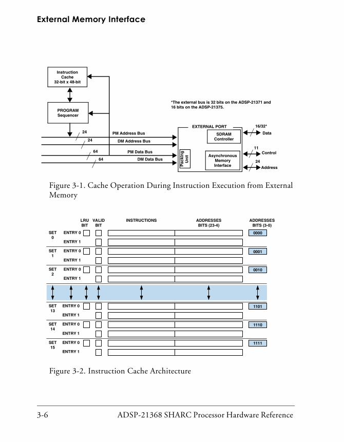
External Memory Interface
3-6 ADSP-21368 SHARC Processor Hardware Reference
Figure 3-1. Cache Operation During Instruction Execution from External Memory
Figure 3-2. Instruction Cache Architecture
PM Address Bus
DM Address Bus
PM Data Bus
DM Data Bus
Pac
kin
gU
nit
SDRAMController
AsynchronousMemoryInterface
PROGRAMSequencer
InstructionCache
32-bit x 48-bit
16/32*
11
24
Data
Control
Address
24
24
64
64
EXTERNAL PORT
*The external bus is 32 bits on the ADSP-21371 and 16 bits on the ADSP-21375.
INSTRUCTIONS
SET0
SET1
SET2
SET13
SET14
SET15
ADDRESSESBITS (23-4)
LRUBIT
VALIDBIT
ENTRY 0
ENTRY 0
ENTRY 0
ENTRY 1
ENTRY 1
ENTRY 1
ENTRY 0
ENTRY 0
ENTRY 0
ENTRY 1
ENTRY 1
ENTRY 1
ADDRESSESBITS (3-0)
0000
0001
0010
1101
1110
1111

ADSP-21368 SHARC Processor Hardware Reference 3-7
External Port
In other words, the 32-entry 2-way set-associative cache in the SHARC has been modified to act as an instruction cache when the program sequencer executes instructions from external memory, while continuing to work as the traditional conflict cache when the sequencer executes instructions located in internal memory. This context switching from con-flict cache to instruction cache and vice-versa happens automatically without the need for any user intervention.
The first time that an instruction from a particular address is fetched from external memory, there is a cache miss when the sequencer looks for this instruction within the cache. Consequently, the instruction has to be fetched from external memory and a copy of instruction is stored in cache. Upon subsequent executions of this instruction, the sequencer search results in a cache hit, resulting in the instruction being fetched from cache instead of external memory. This allows for an instruction throughput that is equivalent to internal memory execution.
This context-dependent caching preserves the cache performance of the traditional SHARC conflict cache as well as significantly improving pro-gram instruction throughput for repetitive instructions such as those inside loops when executing from external memory. Analyses of typical application code examples have shown that this 32-entry instruction cache improves execution throughput by 50-80% over not having this cache.
In general, cache hits occur for all instructions which are fetched and exe-cuted multiple times (for example loops, subroutine calls, negative branches, and so on). Typical applications, such as signal processing algo-rithms, are ideal candidates for significant performance improvements as a result of the cache.
An important and significant result of the instruction being fetched from the cache is that it frees up the external port as well as the internal PM and DM buses for other operations such as data transfers, operand fetches, or DMA transfers.

External Memory Interface
3-8 ADSP-21368 SHARC Processor Hardware Reference
The following example shows the innermost loop of a FIR filter.
lcntr=FILTER_TAPS-1, do macloop until lce;
macloop: f12=f0*f4, f8=f8+f12, f0=dm(i0,m1), f4=pm(i9,m9);
In this example, if the code is stored and executed from external memory, the first time through this loop the program sequencer places the appro-priate 24-bit address on the external address bus, and fetches the instruction in line 2 from external memory. While this instruction is being fetched and processed by the sequencer, it is also simultaneously stored in the internal instruction cache.
For every subsequent iteration of this loop, the instruction is fetched from the internal cache, thereby occurring in a single cycle, while freeing up the internal memory buses to fetch the data operands required for the instruction.
Previously, in the absence of the internal instruction cache, the number of cycles taken by the loop for a case of FILTER_TAPS = 16 would have been a minimum of 48 cycles over a 16-bit wide external bus, and 24 cycles over a 32-bit wide external bus (excluding any conflicts for data operand fetches). However, with the presence of the instruction cache, and assum-ing that the execution is from external SDRAM, and that the instructions are on the same SDRAM page, the number of cycles is reduced to 17 over a 16-bit wide external bus, and either 15 cycles or 16 cycles over a 32-bit wide bus (depending on whether instruction 1 begins on an even 32-bit address, or odd 32-bit address).
Thus, the internal cache improves the efficiency of execution from 16-bit wide external memory by approximately 64.5% for this example.
As might be expected, it is important to remember that the instruction cache will not play a significant role in improving the efficiency of strictly linearly executed code from external memory.

ADSP-21368 SHARC Processor Hardware Reference 3-9
External Port
Instruction Storage and Packing
The ADSP-2137x processors incorporate a 32-bit SDRAM controller. However, the SDRAM controller supports SDRAMs with data bus widths of 16 as well as 32 bits. The packing logic in the SDRAM controller packs the data from SDRAM into 48-bit instructions. Any address produced by the sequencer which falls in external memory is first translated into the physical address in external memory based on the actual data bus width of external memory as shown in Figure 3-3.
The controller completes the required number of accesses from consecu-tive locations for returning a 48-bit word instructions. For a 16-bit SDRAM bus, it performs three accesses. For 32-bit SDRAM, three accesses are performed for two instructions. In this packing mode, all the even addresses in external memory are translated by multiplying the address by a factor of 3/2. For example, if A is an even address falling in external memory region (A > 0x200000), the translated address is ((A>>1) + A). For an odd address, the translated address for the previous even address is incremented by 1. Note that it is the absolute address rather than the offset from the base of external memory that is translated. Therefore, the beginning of external memory, 0x200000, is translated to 0x300000. Two 32-bit accesses are performed for each even address. For an odd address in the sequence, only one access is necessary. Two accesses are necessary however, if the odd address happens to be first in a sequence.
Only bank0 can be populated for external code execution on ADSP-2137x processors.

External Memory Interface
3-10 ADSP-21368 SHARC Processor Hardware Reference
The address range of external memory (asynchronous memory) is shown in Table 3-1. External bank 0 can be used to execute instructions.
Table 3-2 shows the addressable range for SDRAM memory space. Bank 0 can be used for executing instructions. Note that the external memory bank addresses shown are for normal word accesses.
The actual throughput execution from external SDRAM is dependent on the configuration of the SDRAM. The SDRAM can be programmed to run at a number of different frequency ratios with respect to the core clock, the fastest being half of the core clock (or the same as the peripheral clock). The core and SDRAM controller have been enhanced so that
Figure 3-3. Logical Versus Physical Addresses
Table 3-1. External Memory Address Space for Non SDRAM Addresses
Bank Size in words Address Range
Bank 0 14M 0x0020 0000 – 0x00FF FFFF
Bank 1 16M 0x0400 0000 – 0x04FF FFFF
Bank 2 16M 0x0800 0000 – 0x08FF FFFF
Bank 3 16M 0x0C00 0000 – 0x0CFF FFFF
External
ADSP-213xx
Port
External
Bank 0
SequencerPacking
Unit
48
24
“PhysicalAddress” onaddress bus
16/32 bit*“Instruction Data”
on data bus
*32-bit on the ADSP-21371 and 16-bit on the ADSP-21375.
“LogicalAddress” 24
Data
Address
Memory
AddressTranslator

ADSP-21368 SHARC Processor Hardware Reference 3-11
External Port
throughput is maximized when SDRAM is programmed to run at half the core clock frequency and the instructions being fetched are sequential. After the initial latency, accesses follow a 4-2-4-2-4 core cycles pattern for the above setting for a 32-bit SDRAM meaning that because of the way the instructions are packed in external memory, the first instruction takes four core clock cycles to execute, while the second instruction only takes two core cycles, and so on.
It is possible to store both 48-bit instructions as well as 32-bit data in the external memory bank 0. However, care must be taken while specifying the proper starting addresses if 48-bit instructions are stored or interleaved with 32-bit data in the same memory bank. For example, in case of 32-bit wide external SDRAM memory, two instructions are packed into three 32-bit memory locations, while 32-bit data occupies one memory location each. If 2K instructions are placed starting at the bank 0 base address (0x0020 0000), then the starting address for placing data has to be at least 0x0020 0C00 (in other words, an offset of 3K 32-bit words).
The ADSP-2137x processors support the execution of 48-bit wide pro-gram instructions from external memory devices of various widths. The processor can transparently pack and execute instructions stored in 16-bit (ADSP-21375) or 32-bit wide (ADSP-21371) external memory. Table 3-3 shows the format of stored instructions in external 32-bit wide memory. The sequencer automatically places the normal word address corresponding to the starting address of the first instruction to be fetched from external memory on the appropriate address bus, fetches three 16-bit
Table 3-2. External Address Space for SDRAM Memory Accesses
Bank Size in words Address Range
Bank 0 62M 0x0020 0000 – 0x03FF FFFF
Bank 1 64M 0x0400 0000 – 0x07FF FFFF
Bank 2 64M 0x0800 0000 – 0x0BFF FFFF
Bank 3 64M 0x0C00 0000 – 0x0FFF FFFF

External Memory Interface
3-12 ADSP-21368 SHARC Processor Hardware Reference
words and packs them to form the 48-bit instruction to be executed. The address is automatically incremented, and program execution continues with placing the next address on the external address bus, and so on.
In Table 3-3, the logical to physical translation is a multiplication by a factor of 3/2 and N = 0x8AAAA9. Therefore, the 32-bit wide memory supports 8.6 million instructions.
In Table 3-4 the logical to physical translation is a multiplication by a fac-tor of 3 and N = 0x355554. Therefore, the 16-bit wide memory supports 3.3 million instructions.
Table 3-3. Logical Versus Physical Address Mapping, 32-Bit Asynchronous Memory
Logical Address Dispatched by Program Sequencer
Physical Address Observed on the External Address Bus
Data31 0
0x200000 0x300000 Instr0[31:0]
0x300001 Instr1[15:0] Instr0[47:32]
0x200001 0x300001 Instr1[47:16]
0x300002 Instr2[31:0]
0x200002 0x300002 Instr3[15:0] Instr2[47:32]
0x300003 Instr3[47:16]
... ...
...
... ...
...
0xAAAA9 0xFFFFFE InstrN[31:0]
0xFFFFFF 0000 InstrN[47:32]

ADSP-21368 SHARC Processor Hardware Reference 3-13
External Port
Table 3-5 and Table 3-6 show the logical to physical address translation maps for external SDRAM. In SDRAM, there is an additional 2 bits of address generation available to the SDRAM controller. Therefore, the external addressable range is larger than with asynchronous memory and the entire allowable internal address range of 24 bits can be accessed in external memory.
In Table 3-5, N = 0xE00000. Therefore, the total number of external memory instructions for a 32-bit wide SDRAM memory is 14 million.
Table 3-4. Logical Versus Physical Address Mapping, 16-Bit Asynchronous Memory
Logical Address Dispatched by Program Sequencer
Physical Address Observed on the External Address Bus
Data16 0
0x200000 0x600000 Instr0[15:0]
0x600001 Instr0[31:16]
0x600002 Instr0[47:32]
0x200001 0x600003 Instr1[15:0]
0x600004 Instr1[31:16]
0x600005 Instr1[47:32]
0x200002 0x600006 Instr2[15:0]
0x600007 Instr2[31:16]
0x600008 Instr2[47:32]
... ...
... ...
... ...
0x555554 0xFFFFFD InstrN[15:0]
0xFFFFFE InstrN[31:16]
0xFFFFFF InstrN[47:32]

External Memory Interface
3-14 ADSP-21368 SHARC Processor Hardware Reference
In Table 3-6, P = 0xE00000. Therefore, the total number of external memory instructions for a 16-bit wide SDRAM memory is 14 million.
Table 3-5. Logical Versus Physical Address Mapping, 32-Bit SDRAM Memory
Logical Address Dispatched by Program Sequencer
Physical Address Observed on the External Address Bus
Data31 0
0x200000 0x300000 Instr0[31:0]
0x300001 Instr1[15:0] Instr0[47:32]
0x200001 0x300001 Instr1[47:16]
0x300002 Instr2[31:0]
0x200002 0x300002 Instr3[15:0] Instr2[47:32]
0x300003 Instr3[47:16]
... ...
...
... ...
...
0xFFFFFF 0x17FFFFE InstrP[31:0]
0x17FFFFF 0000 InstrN[47:32]
Table 3-6. Logical Versus Physical Address Mapping, 16-Bit SDRAM Memory
Logical Address Dispatched by Program Sequencer
Physical Address Observed on the External Address Bus
Data16 0
0x200000 0x600000 Instr0[15:0]
0x600001 Instr0[31:16]
0x600002 Instr0[47:32]

ADSP-21368 SHARC Processor Hardware Reference 3-15
External Port
Register Configurations for External Memory Execution
If bank 0 memory is asynchronous memory (such as SRAM or flash) then programs need to appropriately configure the asynchronous memory interface control register (AMICTL) and the external port control register (EPCTL). Bits [2:1] of the AMICTL register configure the external bus width as either 16 or 32 bits wide. If bank 0 memory is SDRAM, then programs need to configure the SDRAM control register (SDCTL). Bit 16 determines whether the external bus data width is either 16-bits wide, or 32-bits wide.
The default packing mode on the ADSP-21375 is 16-to-48 bit mode packing, while for the ADSP-21371 it is 32-to-48 bit mode packing.
0x200001 0x600003 Instr1[15:0]
0x600004 Instr1[31:16]
0x600005 Instr1[47:32]
0x200002 0x600006 Instr2[15:0]
0x600007 Instr2[31:16]
0x600008 Instr2[47:32]
... ...
... ...
... ...
0xFFFFFF 0x2FFFFFD InstrN[15:0]
0x2FFFFFE InstrN[31:16]
0x2FFFFFF InstrN[47:32]
Table 3-6. Logical Versus Physical Address Mapping, 16-Bit SDRAM Memory (Cont’d)
Logical Address Dispatched by Program Sequencer
Physical Address Observed on the External Address Bus
Data16 0

External Memory Interface
3-16 ADSP-21368 SHARC Processor Hardware Reference
For the ADSP-21371 processor, the SDCTL register needs to be explicitly programmed for 16-bit wide external memory by setting bit 16 (X16DE) of this register.
EMI Registers and SignalsThe external port global control register is used to set the priority between core and DMA memory accesses and to determine whether SDRAM or asynchronous memory is used on each bank. The bits in this register are described in Table 3-7.
In multiple clock domains, the effect latency of the control register bits of the external port varies. The worst case is 1:4, where the time from a con-trol bit write, to the time the write takes effect, is a maximum of four IOP clock cycles/eight core clock cycles. It is essential to put NOP commands (no operation) in the program to accommodate this time. It is also advised that programs not perform any external memory accesses until the effect takes place. The status bits of the control register can also have a maxi-mum latency of up to one cycle.
The EPCTL register bits should not be changed during external accesses.
Table 3-7. External Port Control Register Bit Descriptions
Bit Name Description Default
0 B0SD Bank 0 SDRAM. 1 = Bank 0 (MS0) connected to SDRAM0 = Bank 0 (MS0) connected to asynchronous memory
0
1 B1SD Bank 1 SDRAM. 1 = Bank 1(MS1) connected to SDRAM0 = Bank 1 (MS1) connected to asynchronous memory
0
2 B2SD Bank 2 SDRAM. 1 = Bank 2 (MS2) connected to SDRAM0 = Bank 2 (MS2) connected to asynchronous memory
0

ADSP-21368 SHARC Processor Hardware Reference 3-17
External Port
3 B3SD Bank 3 SDRAM. 1 = Bank 3 (MS3) connected to SDRAM0 = Bank 3 (MS3) connected to asynchronous memory
0
5–4 EPBR External Port Bus Priority. 11 = Rotating priority 10 = Core has high priority 01 = DMA has high priority00 = Reserved
11
7–6 DMAPR DMA channel Priority for CH0 and CH1. 11 = Rotating priority 10 = Fixed priority 01 = Reserved 00 = Reserved
11
8 Reserved
10–9 FRZDMA Arbitration Freezing Length for DMA. 0 = No freezing 1 = 4 Accesses 2 = 8 Accesses 3 = 16 Accesses
0
12–11 Reserved
14–13 FRZCR Arbitration Freezing Length for CORE Accesses.0 = No freezing 1 = 4 Accesses 2 = 8 Accesses 3 = 16 Accesses
0
18–15 DATE DATA Enable. When the SDRAM/AMI memory con-troller is in no pack mode, these bits of the data lane are masked with zeros. The data lane is 8 bits. The 32-bit data bus has four data lanes. DATA[31:0] is mapped to DL3, DL2, DL1, DL0. For example, if DATE is 1010, then DL3 and DL1 are masked with zeros.
0000
19 Reserved
Table 3-7. External Port Control Register Bit Descriptions (Cont’d)
Bit Name Description Default

External Memory Interface
3-18 ADSP-21368 SHARC Processor Hardware Reference
External Port Arbitration Logic
The external port arbitration logic controls the arbitration between the two DMA channels and processor core. The following control the arbitra-tion logic.
• The EPCTL register can be programmed to use the various features of arbitration between different channels. DMA channels 0 and 1 can be programmed for rotating or fixed priority.
• The winning DMA channel can be arbitrated with the core chan-nel. The EBPR and DMAPR bits define the priorities.
Channel Freezing
The external port is idle when DMA engines are idle and no core access is pending. When multiple DMA channels are reading data from SDRAM memory, channel freezing can improve the data throughput. By setting the freeze bits (FRZDMA, bits 10–9 and FRZCR, bits 14–13), each channel is fro-zen for programmed accesses. For example, if the processor core is frozen for 16 accesses, and if the core requests 16 accesses to SDRAM sequen-tially, data throughput improves. Freezing is based on the fact that sequential accesses to the SDRAM provide better throughput then non-sequential accesses. Freezing does not add value for write accesses. For details on throughput, see “SDRAM Timing” on page 3-74.
Managing Data Paths
The DATE bits (bits 18–15) are used to enable the data paths in the input path. If the DATE bits are set (=1), then the incoming data that corresponds to the set bits are connected to zero. This helps to avoid the floating pin data coming in to the processor.

ADSP-21368 SHARC Processor Hardware Reference 3-19
External Port
External Memory Interface PinsThe pins used by the external memory interface are described in Table 3-8.
Table 3-8. External Memory Pin Descriptions
Pin Name I/O Description for AMI Description for SDRAM
DATA31–0 I/O Data bus Data bus
ADDR23–0 O Address bus Address bus, includes bank selects ADDR [23:0]
SDCLK O N/A SDRAM clock
SDCKE O N/A SDRAM clock enable
SDA10 O N/A SDRAM address bit 10 used for auto refresh
SDRAS O N/A SDRAM row address strobe
SDCAS O N/A SDRAM column address strobe
SDWE O N/A SDRAM write enable
MS3–0 O Chip select Chip select. MS1-0, FLAG2 and FLAG3 are muxed to form MS3-2, (FLAG3 is MS3 and FLAG2 is MS2
RD O Read output strobe N/A
WR O Write output strobe N/A
ACK I Acknowledge signal N/A

Asynchronous Memory Interface
3-20 ADSP-21368 SHARC Processor Hardware Reference
Asynchronous Memory InterfaceBoth the processor core and the I/O processor have access to external memory using the AMI. Table 3-9 describes the processor pins used for interfacing to external memory.
The processor’s memory control signals also permit direct connection to fast static RAM devices. Memory-mapped peripherals and slower memo-ries can also connect to the processor using a user-defined combination of programmable waitstates and hardware acknowledge signals.
External memory can hold data and packed instructions (the ADSP-2136x cannot execute from external memory). Data packing of 16 to 32 bits or 8 to 32 bits is supported for transfers directly from 32-bit, 16-bit, or 8-bit wide external memories to and from internal memory.
Table 3-9. Asynchronous Memory Interface Signals
Pin Type Description
ACK I Memory Acknowledge. External devices can deassert ACK (low) to hold off an external memory access. ACK is used by I/O devices, memory controllers, or other peripherals to hold off completion of an external memory access. ACK has a 22.5 kΩ internal pull-up resistor that is enabled during reset.
ADDR23-0 O External Bus Address. The processor outputs addresses for external memory and peripherals on these pins. A pull-up enabled on the processor’s ADDR23-0 pins maintains the input at the level it was last driven. This pull-up is only enabled on the processor with ID2-0=01x in shared memory system during reset. Note that only the ADSP-21368 processor has shared memory capability.
DATA31–0 I/O External Bus Data. The processor inputs and outputs data on these pins. Pull-up resistors on unused data pins are not necessary. A pull-up on the processor’s DATA31-0 pins maintains the input at the level it was last driven. This pull-up is only enabled on the pro-cessors with ID2-0=01x in shared memory system during reset.

ADSP-21368 SHARC Processor Hardware Reference 3-21
External Port
AMI Timing ControlThe following three sections introduce the available control settings that affect the timing used to make AMI accesses. Note that all accesses are in terms of SDCLK since the SDRAM controller and AMI share this clock.
Wait StatesWait states and acknowledge signals are used to allow the processors to connect to memory-mapped peripherals and slower memories. Wait states are programmable from 1 to 31 using the WS bits (bits 10–6) in the AMI control register. Wait states are programmed relative to SDCLK.
When ACK is enabled, the wait state value should be set to indicate when the processor can sample ACK after the RD/WR edge goes low. The minimum wait state value that can be used is WS = 1 when ACK is enabled. If ACK is not
MS3–0 O Memory Select Lines [FLAG2-3 are muxed and used as MS2 and MS3]. Memory select lines 0–1 are asserted (low) as chip selects for the corresponding banks of external memory. The MS3-0 lines are decoded memory address lines that change at the same time as the other address lines. When no external memory access is occurring, the MS3-0 lines are inactive; they are active however when a condi-tional memory access instruction is executed, whether or not the condition is true.
RD O Memory Read Strobe. RD is asserted whenever the processor reads a word from external memory. In a shared memory system, RD is driven by the bus master. RD has a 22.5 kΩ internal pull-up resistor that is enabled for processors with ID2-0=01x during reset.
WR O Memory Write Strobe. WR is asserted when the processor writes a word to external memory. In a shared memory system, WR is driven by the bus master. WR has a 22.5 kΩ internal pull-up resistor that is enabled for processors with ID2-0=01x during reset.
Table 3-9. Asynchronous Memory Interface Signals (Cont’d)
Pin Type Description

AMI Timing Control
3-22 ADSP-21368 SHARC Processor Hardware Reference
enabled, the minimum value is WS = 2 (a wait state value of 0 corresponds to 32 wait cycles). The processor samples the ACK signal after the pro-grammed wait state count expires—it is imperative that the WS value is initialized when the acknowledge enable bit (ACKEN) is set.
Bus Idle Cycles A bus idle cycle (IC bits 16–14 in the AMICTLx registers) is an inactive bus cycle that the processor automatically generates to avoid data bus driver conflicts. Such a conflict can occur when a device with a long output dis-able time continues to drive after RD is deasserted, while another device begins driving on the following cycle. Idle cycles are also required to pro-vide time for a slave in one bank to three-state its ACK driver, before the slave in the next bank enables its ACK driver in synchronous access modes. Figure 3-4 shows idle cycle insertion between a synchronous read and a zero-wait, synchronous write in cycle 3.
To avoid this data bus driver conflict, the processor generates an idle cycle in the following cases:
• On a transition from a read operation to a write operation
• On a transition from read from one bank to another bank
• On a transition from read from one bank to external access from another device such as an SDRAM controller or another master in a shared memory system
Unlike previous SHARC processors, the ADSP-21367/8/9 and ADSP-2137x SHARC processors do not support idle cycle inser-tion on a page boundary crossing. If an idle cycle is programmed for a particular bank, then a minimum of one cycle is inserted for reads, even if they are from the same bank.

ADSP-21368 SHARC Processor Hardware Reference 3-23
External Port
Bus Hold CyclesThe processor is able to insert bus hold and read hold cycles by setting bits in the AMI control register (AMICTLx). These two methods for holding off data processing are described below.
• Bus hold cycle (HC bits 13–11) is an inactive bus cycle that the pro-cessor automatically generates at the end of a read or write to allow a longer hold time for address and data. Programs may disable holds, or hold off processing for one or more external port proces-sor cycles.
• Read hold cycle (RHC bits 20–18) is the delay between two reads at the end of a read access. Programs may disable the read hold cycle, or hold the address for one or more external port clock cycles.
Figure 3-4. Idle Cycle Example, Wait State = 2
1 2 3 4 5
SDCLK
ADDRESS 23-0
MSx
RD
WR
DATA 31-0
READ IDLE WRITE
6

Setting AMI Modes
3-24 ADSP-21368 SHARC Processor Hardware Reference
The address, data (if a write), and bank select (if in banked external mem-ory) remain unchanged and are driven for one or more cycles after the read or write strobes are deasserted. Figure 3-5 demonstrates a hold time cycle appended to an asynchronous write access (EBxWS = 011).
Setting AMI ModesThe AMICTLx registers control the asynchronous memory interface’s oper-ating mode and the AMISTAT register provides status information. Table A-5 on page A-18 lists all the bits in the AMICTLx registers and Figure A-7 on page A-20 shows all the bits in the AMISTAT register.
• For information on using DMA through the external port, see “External Port DMA” on page 2-35.
• For information on using external port interrupts, see “Inter-rupt-Driven I/O” on page 2-6.
Figure 3-5. Hold Time Cycle Example
1 2 3 4 5
SDCLK
ADDRESS 23-0
MSx
WR
DATA 31-0
HOLDTIME
WRITE

ADSP-21368 SHARC Processor Hardware Reference 3-25
External Port
There is a 3:1 bus conflict resolution ratio at the external port interface (three internal buses to one external bus) in addition to the 2:1 or greater clock ratio between the processor’s internal clock and the external SDRAM clock (SDCLK). Systems that fetch data through the external port must tolerate at least one cycle—and pos-sibly many additional cycles—of latency for non-SDRAM accesses.
Data alignment through the external port is identical for these interfaces.
External Memory ReadsThe AMI behaves as an external port bus slave and an external read access is performed only upon a read request from the external port control bus. Reads from external memory are done through the AMI. When an exter-nal address that is mapped to the AMI in the EPCTL register is accessed, the module receives 8-, 16-, or 32-bit data and packs the data based on the packing and control modes in the AMI control register (AMICTLx). Once the data is received, the status bit RXS is set, indicating valid data is present. Updates occur on a feedback RD signal and the status update occurs on the SDCLK signal. The RXS status update is delayed by one cycle to accommodate the delay in the feedback RD signal.
The AMI provides the interface to the external data pins as well as to the processor core or to the internal DMA controller. When the AMI receives data, it is passed by internal hardware to the DMA controller or to the external port control bus, depending on which entity requested the data.
Data Packing
Data packing for memory reads is accomplished using the packing disable (PKDIS, bit 3) and most significant word first (bit 4 in the MSWF register) bits in the AMICTLx register.
For packed data mode where PKDIS = 0 and MSWF = 0, the packing order for BW = 8 is: first byte is bits [7–0], the second byte is bits [15–8], and so on.

Setting AMI Modes
3-26 ADSP-21368 SHARC Processor Hardware Reference
For packed data mode where PKDIS = 0 and MSWF = 1, the packing order for BW = 8 is: first byte received is bits 31–24, the second byte is bits 23–15, and so on.
If the PKDIS bit is set (=1), then the 8- or 16-bit data (based on the bus width) is zero appended to 32 bits.
Both of these methods apply to 16- to 32-bit packing as well. These modes are summarized in Table 3-10.
External Memory WritesThe AMI behaves as an external port bus slave and external write accesses are performed when there is a write request from the external port control bus. Writes to external memory are done through the AMI module. When an external address that is mapped to the AMI in the EPCTL register is accessed, the module receives data from internal memory using the DMA
Table 3-10. Data Packing Bit Settings (Reads)
Packing Mode
PKDIS Bit Setting
MSWF Bit Setting Description
Enabled 0 0 8- or 16-bit received data is packed to 32-bit data and transmitted 32-bit data is unpacked to two 16-bit data or four 8-bit data. First 8- or 16-bit word read/written occupies the least significant position in the 32bit packed word.
Enabled 0 1 8 or 16 bit received data is packed to 32-bit data and 32-bit data to be transmitted is unpacked to two 16-bit data or four 8-bit data. First 8- or 16-bit word read/written occupies the most significant position in the 32-bit packed word.
Disabled 1 N/A 8- or 16-bit data received is zero filled. For transmit-ted data only 16-bit or the 8-bit LSB part of the 32-bit data word is written to external memory.

ADSP-21368 SHARC Processor Hardware Reference 3-27
External Port
controller or through direct core writes. Writes to the AMI set a status bit (AMITXS, bit 2 in the AMISTAT register) and initiate the external write access.
Once a full word is transferred out of the AMI, the AMITXS bit is cleared and new writes are allowed. No more external transfers can start while the AMI module is empty.
Whenever the AMITX is empty, the DMA controller or a direct access from the processor core can write fresh data into the AMI. If the register is full, further writes from the core (or DMA controller) are stalled.
Data Packing
Data unpacking for memory writes uses the packing disable bit (PKDIS, bit 3) and the most significant word first (MSWF, bit 4) bits in the AMICTLx register.
For packed data mode where PKDIS = 0 MSWF = 0, the order of unpacking for 32- to 8-bit data is: the first byte is bits 7–0, the second byte is bits 15–8, and so on.
For packed data mode where PKDIS = 0 MSWF = 1, the unpacking order for 32- to 8-bit data is: first byte received is bits 31–24, the second byte is bits 23–16, and so on.
If PKDIS bit is set (=1), only the 16- or 8-bit least significant portion of the 32-bit data is written to external memory.
Both of these methods apply to 32- to 16-bit unpacking as well. These modes are summarized in Table 3-10.
For direct access (core and DMA), the received data is also unpacked, depending on the setting of the PKDIS bit. The order of unpacking is dependent on the MSWF bit in AMICTLx registers.

Setting AMI Modes
3-28 ADSP-21368 SHARC Processor Hardware Reference
Read/Write ThroughputFor a wait state of 2 (which is the smallest wait state), the throughput is shown in Table 3-11.
External Access AddressingThe AMI supports 16M words of external memory in bank1, bank2, and bank3 and 14M words of external memory in bank0. The maximum amount of external data is 64M bytes when the external bus width (set using the BW bits 2–1 in the AMICTLx registers) is 32 bits on bank1, bank2, or bank3.
The ADSP-21367/8/9 and ADSP-2137x processors have the ability to use logical addressing when an external memory smaller than 32 bits is used. When logical addresses are used, multiple external addresses seen by the memory correspond to a single internal address, depending on the width of the memory being accessed, and the packing mode setting of the AMI or SDRAM controller. The following are examples of logical addressing.
Table 3-11. Read/Write Throughput
Bus Width Operation Throughput in SDCLK Cycles
32-bit Write One 32-bit word per 3 SDCLK cycles
32-bit Read One 32-bit word per 3 SDCLK cycles
16-bit Write One 32-bit word per 6 SDCLK cycles
16-bit Read One 32-bit word per 6 SDCLK cycles
8-bit Write One 32-bit word per 12 SDCLK cycles
8-bit Read One 32-bit word per 12 SDCLK cycles

ADSP-21368 SHARC Processor Hardware Reference 3-29
External Port
• For an external bus width of 32 bits, or when packing is disabled with other bus widths (PKDIS = 1 and BW = 16 bits or PKDIS = 1 and BW = 8 bits), then the external physical memory is the same as the lower 24 bits of bits 23–0 in the address being supplied to the external port by the core or DMA controller.
• For an external bus width of 16 bits with packing enabled (PKDIS = 0), the external physical address ADDR23–0 generation is ADDR23–1 = bits 22–0 in the address being supplied to the external port by the core or DMA controller. Here, ADDR[0] corresponds to the 1st/2nd 16-bit word.
• For an external bus width of 8 bits with packing enabled (PKDIS = 0), the external physical address ADDR23–0 generation is ADDR23–2 = bits 21–0 in the address being supplied to the external port by the core or DMA controller. Here, ADDR1–0 corresponds to the 1st/2nd/3rd/4th 8-bit word.
The external physical address map is shown in Table 3-12.
Table 3-12. AMI Address Memory Map
Bus Width External Memory BANK
External Physical Address (on ADDR23–0)
32-bit (or PKDIS=1) 0 0x20_0000 to 0xFF_FFFF
32-bit (or PKDIS=1) 1, 2, and 3 0x00_0000 to 0xFF_FFFF
16-bit (and PKDIS=0) 0 0x40_0000 to 0xFF_FFFF
16-bit (and PKDIS=0) 1, 2, and 3 0x00_0000 to 0xFF_FFFF
8-bit (and PKDIS=0) 0 0x80_0000 to 0xFF_FFFF
8-bit (and PKDIS=0) 1, 2, and 3 0x00_0000 to 0xFF_FFFF

SDRAM Controller
3-30 ADSP-21368 SHARC Processor Hardware Reference
External Port DMAThe AMI shares the two DMA channels of the external port with the SDRAM controller. Either of these DMA channels can be directed to the external asynchronous memories. For information on external port DMA, see Chapter 2, I/O Processor.
Booting Through the AMIThe AMI supports an 8-bit user boot called AMI boot. For more informa-tion, see “Booting Through the AMI” on page 14-39.
SDRAM ControllerThe ADSP-21367/8/9 and ADSP-2137x SHARC processors support a glueless interface with any of the standard SDRAMs of 64M bit, 128M bit, 256M bit, and 512M bit with configurations x4, x8, x16 and x32. The SDRAM controller (SDC) can support up to 254M words of SDRAM in four banks. Bank 0 can accommodate up to 62M words, and banks 1, 2, and 3 can accommodate up to 64M words each. The SDC includes timing options to support additional buffers between the proces-sors and SDRAM. This allows the processor to handle the capacitive loads of large memory arrays. The following are additional features of the SDC.
• I/O width 16-bit or 32-bits, I/O supply 3.3 V
• Types of 32, 64, 128, 256, and 512M bit with I/O of x4, x8, x16 and x32
• Page sizes of 128, 256, 512, 1k, 2k words
• SDC uses no-burst mode (BL = 1) with sequential burst type
• SDC uses optional full page burst (ADSP-2137x only)

ADSP-21368 SHARC Processor Hardware Reference 3-31
External Port
• SDC uses open page policy—any open page is closed only if a new access in another page of the same bank occurs
• Supports multibank operation within the SDRAM (ADSP-2137x only)
• Uses a programmable refresh counter to coordinate between vary-ing clock frequencies and the SDRAM’s required refresh rate
• Provides multiple timing options to support additional buffers between the processor and SDRAM
• Allows independent auto-refresh while the asynchronous memory interface (AMI) has control of the External Port
• Supports self-refresh mode for power savings
• Supports instruction fetch (ADSP-2137x only)
• Supports 32-bit data access by the processor core
All inputs are sampled and all outputs are valid on the rising edge of the SDRAM clock output (SDCLK).
Definition of TermsThe following are terms commonly used in SDRAM systems.
Bank activate command
The bank activate command causes the SDRAM to open an internal bank of memory (specified by the bank address) in a specific row (specified by the row address). For more information, see “SDC Commands” on page 3-63.

SDRAM Controller
3-32 ADSP-21368 SHARC Processor Hardware Reference
Burst length
The burst length determines the number of words that the SDRAM device stores or delivers after detecting a single write or read command, respectively.
The SDC supports burst length = 1 mode only.
Burst stop command
Use of this command is one of several ways to terminate or interrupt a burst read or write operation. Since the burst length is hardwired to 1, the SDC does not support the burst stop command. However, this command is optionally supported by ADSP-2137x processors.
Burst type
The burst type determines the address order in which the SDRAM deliv-ers burst data after detecting a read command, or stores burst data after detecting a write command.
Since the burst length is always programmed to 1, the burst type does not apply. However, the SDC always sets the burst type to sequen-tial-accesses-only during the SDRAM power-up sequence.
CAS latency
Also tAA, tCAC. The column address strobe (CAS) latency is the delay in clock cycles between when the SDRAM detects the read command and when it provides the data at its output pins. The CAS latency is pro-grammed in the SDRAM mode register during the power-up sequence with the value programmed in the SDRAM control register (SDCTL bits 1-0).
The speed grade of the SDRAM and the SDCLK frequency determine the value of the CAS latency. The SDC supports CAS latencies of 2 or 3 clock cycles. The selected CAS latency value is programmed into the SDCTL reg-ister before the SDRAM power-up sequence.

ADSP-21368 SHARC Processor Hardware Reference 3-33
External Port
CBR (CAS before RAS)
Refresh or auto-refresh. When the SDC refresh counter times out, the SDC precharges all four banks of SDRAM and then issues an auto-refresh command to them. This causes the SDRAMs to generate an internal CBR refresh cycle. When the internal refresh completes, the SDRAM banks are precharged.
Data mask feature
SDRAM’s allow partial read or writes in byte addressing mode. Since SHARC processors do not support byte addressing, DQM pins are not con-trolled by the SDC.
Internal bank
There are several internal memory banks on a given SDRAM row. An internal bank in a specific row cannot be activated (opened) until the pre-vious internal bank in that row has been precharged.
The SDC does not support multibank accesses. The bank address can be thought of as part of the row address. The SDC also assumes that all SDRAMs to which it interfaces have four internal banks.
Only the SDRAM controller on the ADSP-2137x processors sup-ports multibank accesses.
Mode register
SDRAM devices contain an internal configuration register which allows specification of the SDRAM device’s functionality. During power-up, and before executing a read or write to the SDRAM memory space, the appli-cation must trigger the SDC to write to the SDRAM’s mode register. The write of the this register is triggered by writing a 1 to the SDPSS bit (bit 14) in the processor’s SDRAM control register (SDCTL), and then issuing a read or write transfer to the SDRAM address space.

SDRAM Controller
3-34 ADSP-21368 SHARC Processor Hardware Reference
The initial read or write triggers the SDRAM power-up sequence, which programs the SDRAM’s mode register with the CAS latency from the SDCTL register. This initial read or write to SDRAM takes many cycles to complete. Note that for most applications the SDRAM power-up sequence and a write to the mode register is performed only once. Once the power-up sequence has completed, the SDPSS bit should not be set again unless a change to the mode register is desired.
Page size
Page size is the amount of memory which has the same row address and can be accessed with successive read or write commands without needing to activate another row.
Precharge command
The precharge command closes a specific internal bank in the active page or all internal banks in the page. For more information, see “SDC Com-mands” on page 3-63.
Self-refresh
When the SDRAM is in self-refresh mode, its internal timer initiates auto-refresh cycles periodically, without external control input. The SDC must issue a series of commands, including the self-refresh command, to put the SDRAM into this low power mode. It must issue another series of commands to exit self-refresh mode. Entering self-refresh mode is pro-grammable in the SDRAM control register (SDCTL) and any access to the SDRAM address space causes the SDC to exit the SDRAM from self-refresh mode. For more information, see “Self-Refresh Mode” on page 3-70.

ADSP-21368 SHARC Processor Hardware Reference 3-35
External Port
tRAS
Required delay between issuing a bank activate command and a precharge command, and between issuing the self-refresh command and the exit from self-refresh mode. The SDTRAS bits (7–4) in the SDCTL register can be set to 1 to 15 clock cycles.
tRP
Required delay between issuing a precharge command and issuing:
• a bank activate command
• an auto-refresh command
• a self-refresh command
The SDTRP bits (10–8) in the SDCTL register can be set to 1 to 7 clock cycles.
tMRD
Required delay between issuing a mode register set command and a suc-cessive bank activate command. This delay is not directly programmable and is assumed to be 2 clock cycles.
tRCD
Required delay between a bank activate command and the start of the first read or write command. The SDTRCD bits (26–24) in the SDCTL register can be set to 1 to 7 clock cycles.
tWR
Required delay between a write command (driving write data) and a pre-charge command. The SDTWR bits (18–17) in the SDCTL register can be set to 1 to 3 clock cycles.

SDRAM Controller
3-36 ADSP-21368 SHARC Processor Hardware Reference
tRC
Required delay between issuing successive bank activate commands to the same SDRAM internal bank. This delay is not directly programmable. The tRC delay is satisfied by programming the SDTRAS and SDTRP fields to ensure that tRAS + tRP ≥ tRC.
tRFC
Required delay between issuing an auto-refresh command and a bank acti-vate command, and between issuing successive auto-refresh commands. This delay is not directly programmable and is assumed to be equal to tRC. The tRC delay is satisfied by programming the SDTRAS and SDTRP fields to ensure that tRAS + tRP ≥ tRC.
tRRD
This is the required delay between a bank A activate command and a bank B activate command. This delay is not programmable and fixed to tRCD + 1 cycles. This delay is used for multibank operation (ADSP-2137x processors only).
tXSR
Required delay between exiting the self-refresh mode and issuing an auto-refresh command. This delay is not directly programmable and is assumed to be equal to tRC. The tRC delay is satisfied by programming the tRAS and tRP fields to ensure that tRAS + tRP ≥ tRC.
Timing External Memory AccessesThe SDRAM controller is capable of running at up to 166 MHz and can run at various frequencies, depending on the programmed SDRAM clock (SDCLK) to core clock (CCLK) ratios. These are shown in Table 3-13.
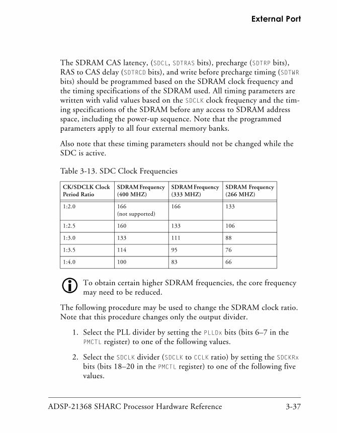
ADSP-21368 SHARC Processor Hardware Reference 3-37
External Port
The SDRAM CAS latency, (SDCL, SDTRAS bits), precharge (SDTRP bits), RAS to CAS delay (SDTRCD bits), and write before precharge timing (SDTWR bits) should be programmed based on the SDRAM clock frequency and the timing specifications of the SDRAM used. All timing parameters are written with valid values based on the SDCLK clock frequency and the tim-ing specifications of the SDRAM before any access to SDRAM address space, including the power-up sequence. Note that the programmed parameters apply to all four external memory banks.
Also note that these timing parameters should not be changed while the SDC is active.
To obtain certain higher SDRAM frequencies, the core frequency may need to be reduced.
The following procedure may be used to change the SDRAM clock ratio. Note that this procedure changes only the output divider.
1. Select the PLL divider by setting the PLLDx bits (bits 6–7 in the PMCTL register) to one of the following values.
2. Select the SDCLK divider (SDCLK to CCLK ratio) by setting the SDCKRx bits (bits 18–20 in the PMCTL register) to one of the following five values.
Table 3-13. SDC Clock Frequencies
CK/SDCLK Clock Period Ratio
SDRAM Frequency (400 MHZ)
SDRAM Frequency (333 MHZ)
SDRAM Frequency(266 MHZ)
1:2.0 166 (not supported)
166 133
1:2.5 160 133 106
1:3.0 133 111 88
1:3.5 114 95 76
1:4.0 100 83 66
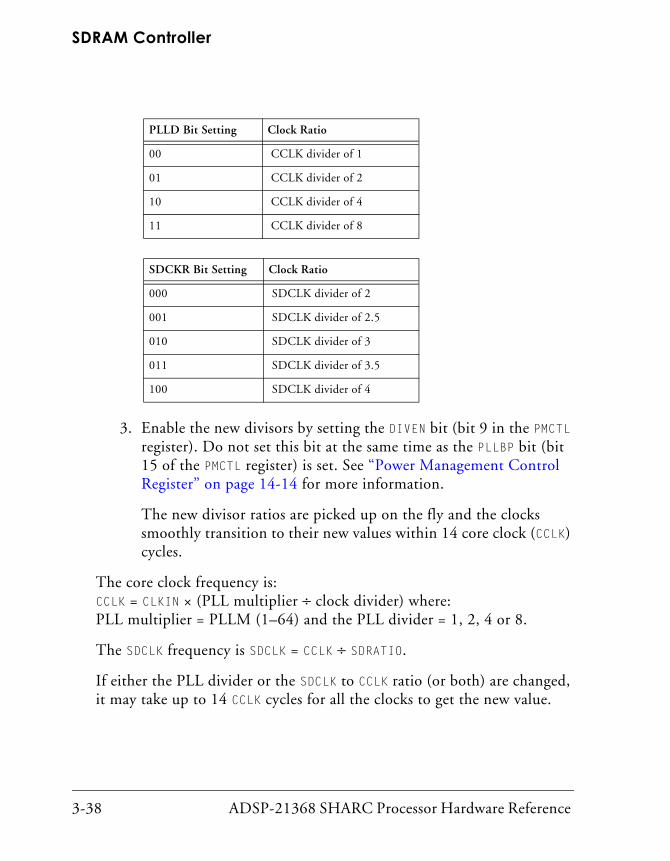
SDRAM Controller
3-38 ADSP-21368 SHARC Processor Hardware Reference
3. Enable the new divisors by setting the DIVEN bit (bit 9 in the PMCTL register). Do not set this bit at the same time as the PLLBP bit (bit 15 of the PMCTL register) is set. See “Power Management Control Register” on page 14-14 for more information.
The new divisor ratios are picked up on the fly and the clocks smoothly transition to their new values within 14 core clock (CCLK) cycles.
The core clock frequency is: CCLK = CLKIN × (PLL multiplier ÷ clock divider) where: PLL multiplier = PLLM (1–64) and the PLL divider = 1, 2, 4 or 8.
The SDCLK frequency is SDCLK = CCLK ÷ SDRATIO.
If either the PLL divider or the SDCLK to CCLK ratio (or both) are changed, it may take up to 14 CCLK cycles for all the clocks to get the new value.
PLLD Bit Setting Clock Ratio
00 CCLK divider of 1
01 CCLK divider of 2
10 CCLK divider of 4
11 CCLK divider of 8
SDCKR Bit Setting Clock Ratio
000 SDCLK divider of 2
001 SDCLK divider of 2.5
010 SDCLK divider of 3
011 SDCLK divider of 3.5
100 SDCLK divider of 4

ADSP-21368 SHARC Processor Hardware Reference 3-39
External Port
For more information on SDRAM clocking and programming the PLL, see “Clock Derivation” on page 14-13, “Power Management Control Reg-ister” on page 14-14, and “Power Management Control Register (PMCTL)” on page A-170.
Parallel Connection of SDRAMsTo specify a SDRAM system, multiple possibilities are given based on the different memory sizes. For a 32-bit I/0 capability, the following can configured.
• 1 x 32-bit/page 256 words
• 2 x 16-bit/page 512 words
• 4 x 8-bit/page 1k words
• 8 x 4-bit/page 2k words
The SDRAM’s page size is used to determine the system you select. All four systems have the same external bank size, but different page sizes. Note that larger page sizes, allow higher performance but larger page sizes require more complex hardware layouts.
Even if connecting SDRAMs in parallel, the SDC always considers the cluster as one external SDRAM bank because all address and control lines feed the parallel parts.
SDRAM Control Register (SDCTL)The SDRAM memory control register includes all programmable parame-ters associated with the SDRAM access timing and configuration. These bits are described below. For more information, see “SDRAM Control Register (SDCTL)” on page A-21.

SDRAM Controller
3-40 ADSP-21368 SHARC Processor Hardware Reference
SDRAM CAS latency parameter setting. SDCL bits 1–0. The column address strobe (CAS) latency is the delay in clock cycles between when the SDRAM detects the read command and when it provides the data at its output pins. Settings are: 10 = 2 cycles, 11 = 3 cycles.
Generally, the frequency of operation determines the value of the CAS latency. For specific information about setting this value, consult the SDRAM device documentation.
SDRAM controller disable. DSDCTL bit 2. Enables or disables the SDC. If DSDCTL is set (=1), any access to SDRAM address space does not occur externally. All SDC control pins are in their inactive states and the SDRAM clock, SDCLK, does not run.
The DSDCTL bit is cleared (=0) by default, so that SDCLK is running after reset deasserts. If the SDC is not used, the DSDCTL bit can be set to stop the clock and reduce power dissipation. Even though the SDC is enabled at reset, the power-up sequence must be executed before reading or writing to SDRAM address space. Failure to execute the power-up sequence before reading or writing to SDRAM address space results in unpredict-able operation. However, DSDCTL must remain cleared at all times when the SDC is needed to generate auto-refresh commands to the SDRAM.
SDRAM tRAS parameter setting. SDTRAS bits 7–4. The tRAS value (bank activate command delay) defines the required delay, in number of SDCLK cycles, between the time the SDC issues a bank activate command and the time it issues a precharge command as shown below.
The SDRAM must also remain in self-refresh mode for a period of time of at least tRAS. The tRP and tRAS values define the tRFC, tRC, and tXSR val-ues. For more information, see “Timing External Memory Accesses” on page 3-36.
SDTRAStRASmintSDCLK
--------------------≥

ADSP-21368 SHARC Processor Hardware Reference 3-41
External Port
The tRAS parameter allows the ADSP-21367/8/9 and ADSP-2137x pro-cessors to adapt to the timing requirements of the system’s SDRAM devices. Any value between 1 and 15 SDCLK cycles can be selected as shown in Table 3-14.
SDRAM tRP parameter setting. SDTRP bits 10–8. Defines the required precharge delay, in number of SDCLK cycles, between the time the SDC issues a precharge command and the time it issues a bank activate com-mand as shown in the following equation.
The tRP setting also specifies the time required between precharge and auto-refresh, and between precharge and self-refresh. Any value between 1 and 7 SDCLK cycles may be selected as shown in Table 3-15.
Table 3-14. Bank Activate Command Delay Bit Settings
Bit Setting Clock Cycles Bit Setting Clock Cycles
SDTRAS1 = 0000 Reserved SDTRAS8 = 1000 8
SDTRAS1 = 0001 1 SDTRAS9 = 1001 9
SDTRAS2 = 0010 2 SDTRAS10 = 1010 10
SDTRAS3 = 0011 3 SDTRAS11 = 1011 11
SDTRAS4 = 0100 4 SDTRAS12 = 1100 12
SDTRAS5 = 0101 5 SDTRAS13 = 1101 13
SDTRAS6 = 0110 6 SDTRAS14 = 1110 14
SDTRAS7 = 0111 7 SDTRAS15 = 1111 15
SDTRPtRPmintSDCLK------------------≥

SDRAM Controller
3-42 ADSP-21368 SHARC Processor Hardware Reference
SDRAM power-up mode. SDPM bit 11. If the SDPM bit is set (=1), the SDC does a precharge all command, followed by a load mode register com-mand, and eight auto-refresh cycles. If the SDPM bit is cleared (=0), the SDC does a precharge all command, followed by eight auto-refresh cycles, and a load mode register command.
SDRAM bank column address width. SDCAW bits 13–12 shown in Table 3-16. Sets the SDRAM page size. Page sizes of 256 and 512 bits, and 1K and 2K bits are supported. Table 3-22 on page 3-53 shows the page size and breakdown of the internal address (IA31–0), as seen from the core into the row, bank, and column address. The column address makes up the address inside the page.
Programming the SDC with non-supported page size values pro-duces unpredictable results.
Table 3-15. Precharge Delay Bit Settings
Bit Setting Clock Cycles Bit Setting Clock Cycles
000 Reserved SDTRP4 = 100 4
SDTRP1 = 001 1 SDTRP5 = 101 5
SDTRP2 = 010 2 SDTRP6 = 110 6
SDTRP3 = 011 3 SDTRP7 = 111 7
Table 3-16. SDRAM Bank Column Address Width Bit Settings
SDCAW Bit Setting SDRAM Bank Column Address Width
SDCAW8 = 00 8 bits (256 words)
SDCAW9 = 01 9 bits (512 words)
SDCAW10 = 10 10 bits (1K words)
SDCAW11 = 11 11 bits (2K words)

ADSP-21368 SHARC Processor Hardware Reference 3-43
External Port
SDRAM power-up sequence start. SDPSS bit 14. The SDPM bit specifies the power-up mode and the SDPSS bit starts an SDRAM power-up (initial-ization) sequence. When this bit is set (=1), the SDRAM power-up sequence starts on the next SDRAM access. When cleared, this bit has no effect. This bit always reads zero. See also “Load Mode Register” on page 3-64.
SDRAM self-refresh command. SDSRF bit 15. When set (=1), starts the self-refresh mode. When cleared (=0) this bit has no effect. This bit always reads zero. In self-refresh mode, the SDRAM performs refresh operations internally which reduces the SDRAM’s power consumption.
When SDSRF is set to 1, the SDC enters an idle state. In this state, it issues a precharge command (if necessary) and then issues a self-refresh com-mand. If an internal access is pending, the SDC delays issuing the self-refresh command until it completes all pending SDRAM access requests. Once the SDRAM device enters into self-refresh mode, the SDRAM controller asserts the SDSRA bit in the SDRAM control status reg-ister (SDSTAT). The SDRAM controller ignores other self-refresh requests when the SDRAM device is already in self-refresh mode.
The SDRAM device exits self-refresh mode only when the SDC receives a request for SDRAM space access. There is no way to can-cel entry into self-refresh mode.
SDRAM external data path width. X16DE bit 16. Selects whether the SDRAM interface is 32 or 16 bits wide.
• If set (=1), a 16-bit SDRAM should be used; DATA[15–0] should be connected to the SDRAM data pins; ADDR[14:0] should be connected to SDRAM address pins 14–0; 16 to 32-bit packing is performed.Note that ADDR[18:17] pins are also used. See tables Table 3-22 on page 3-53 to Table 3-25 on page 3-57 for bank address usage.

SDRAM Controller
3-44 ADSP-21368 SHARC Processor Hardware Reference
• If cleared (=0), a 32-bit SDRAM should be used; DATA[31–0] should be connected to the SDRAM data pins; ADDR[15:1] should be connected SDRAM address pins 14–0. For more information, see “SDRAM Address Mapping” on page 3-51.Note that ADDR[18:17] pins are also used. See tables Table 3-22 on page 3-53 to Table 3-25 on page 3-57 for bank address usage.
SDRAM tWR parameter setting. SDTWR bits 18–17. Defines the required delay, in number of SDCLK cycles, between the time the SDC issues a write command (drives write data) and a precharge command.
The tWR parameter enables applications to accommodate the SDRAM’s timing requirements. For more information, see “Timing External Mem-ory Accesses” on page 3-36. Any value between 1 and 3 SDCLK cycles may be selected as shown in Table 3-17.
SDRAM optional refresh. SDORF bit 19. Used for memories built as SDRAM in FPGAs. When set (=1), auto-refresh is not performed and the Force AR bit does not have any effect. When cleared (=0), auto-refresh occurs when the refresh counter expires. See also “SDRAM Refresh Rate Control Register (SDRRC)” on page 3-49.
Table 3-17. SDRAM tWR Bit Settings
SDTWR Bit Setting SDRAM Parameter Setting
00 Reserved
SDTWR1 = 01 One clock cycle
SDTWR2 = 10 Two clock cycles
SDTWR3 = 11 Three clock cycles
SDTWRtWRmin
tSDCLK------------------≥

ADSP-21368 SHARC Processor Hardware Reference 3-45
External Port
Force auto-refresh. Force AR bit 20. When set (=1), forces auto-refresh. When cleared (=0), has no effect. Note that when SDORF bit is set, setting this bit causes Force AR to have no effect.
Force precharge. Force PC bit 21. When set (=1), forces precharge. When cleared (=0), has no effect.
Force load mode register. Force LMR bit 22. If set (=1), when SDRAMs are in a precharged state, a mode register write to SDRAMs is initiated immediately. This is in contrast to the normal load mode register set which requires some delay. This command performs a precharge all (if not precharged already) followed by a mode register write (ADSP-2137x pro-cessors only).
External register buffer pipeline option. SDBUF bit 23. Enables, if set (=1), or disables, if cleared (=0), external buffer timing. When buffered SDRAM modules or discrete register buffers are used to drive the SDRAM control inputs, SDBUF should be set to 1. This adds a cycle of data buffer-ing to read and write accesses. An example single processor system is shown in Figure 3-7.
When no buffering is required, the example shown in Figure 3-6 can be used.
SDRAM tRCD parameter setting. SDTRCD bits 26–24. Sets the required delay (in terms of SDCLK) between a bank activate command and the start of the first read or write command.
SDRCDtRCDmin
tSDCLK---------------------=
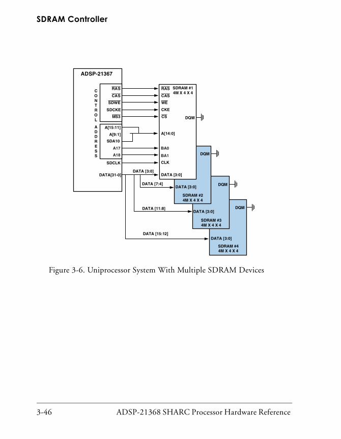
SDRAM Controller
3-46 ADSP-21368 SHARC Processor Hardware Reference
Figure 3-6. Uniprocessor System With Multiple SDRAM Devices
SDRAM #44M X 4 X 4
DATA [3:0]
DQM
DATA[31-0]
ADSP-21367
MS3
RAS
CAS
SDWE
SDCKE
CONTROL
RAS
CAS
DQM
WE
CLK
CKE
SDRAM #14M X 4 X 4
DATA [3:0]
A[14:0]
CS
SDRAM #24M X 4 X 4
SDRAM #34M X 4 X 4
DATA [3:0]
DATA [3:0]
DATA [7:4]
DATA [11:8]
DATA [3:0]
BA1
BA0
ADDRESS
SDCLK
A[15:11]
A[9:1]
SDA10
A17
A18 DQM
DQM
DATA [15:12]

ADSP-21368 SHARC Processor Hardware Reference 3-47
External Port
Figure 3-7. Uniprocessor System With Multiple Buffered SDRAM Devices
SDRAM #84 X 4 X 4
DATA[3:0]
DQM
SDRAM #74 X 4 X 4
SDRAM #64 X 4 X 4
DATA[31-0]
ADSP-21367
MS3
RAS
CAS
SDWE
SDCLK
SDCKE
CONTROL
REGISTEREDBUFFERS
I0
I5
I4
I2
I1
O0A
O4A
O3A
O2A
O1A
IX[14:0]
OXA[14:0]
OXB[14:0]
RAS
CAS
WE
CLK
CKE
SDRAM #54 X 4 X 4
DATA [3:0]
A[14:0]
CS
DATA[3:0]
AB[15:1]
AA[15:1]
D Q
D Q
ADDR [15]
CTRL [6]
21
21
SDRAM BANK 1ADDR & CTRL
SDRAM BANK 2ADDR & CTRL
DATA[3:0]
ADDRESS
A[15:11]
A[9:1]
SDA10
A17
A18
DQM
DQM
DQM
DATA [31:28]
DATA [19:16]
DATA [23:20]
O0B
O4B
O3B
O2B
O1B
TO SDRAM #1, 2, 3, 44 X 4 X 4
DATA [15:12]
DATA [7:4]
DATA [11:8]
DATA [3:0]
DATA [27:24]

SDRAM Controller
3-48 ADSP-21368 SHARC Processor Hardware Reference
For more information, see “Timing External Memory Accesses” on page 3-36. Any value between 1 and 7 SDCLK cycles may be selected as shown in Table 3-18.
SDRAM row address width. SDRAW bits 29–27. With the X16DE and SDCAW bits, defines the SDRAM core memory space (internal address to external address mapping). Any value between 0 to 7 can be selected as shown in Table 3-19. For more information, see “SDRAM Address Mapping” on page 3-51.
Program the SDRAM Controller for Page Size of 128 Words. PGSZ 128 bit 30. This bit allows programs to configure the SDC for a page size of 128 words (7 bits) which supports most available 32 Mb SDRAMs.
No burst mode. NO BSTOP bit 31. This bit is used to select between full page burst or no burst mode (BL=1). If set (=1), no burst mode is active and the burst stop command is ignored. If cleared, full page burst is active using the burst stop command for access interruption. This bit must be cleared if the SDRAM does not support no burst mode but supports full page burst.
Table 3-18. SDRAM tRCD Bit Settings
SDTRCD Bit Setting
SDRAM Parameter Setting
SDTWR Bit Setting
SDRAM Parameter Setting
000 Reserved STDRCD4 = 100 Four clock cycles
STDRCD1 = 001 One clock cycle STDRCD5 = 101 Five clock cycles
STDRCD2 = 010 Two clock cycles STDRCD6 = 110 Six clock cycles
STDRCD3 = 011 Three clock cycles STDRCD7 = 111 Seven clock cycles

ADSP-21368 SHARC Processor Hardware Reference 3-49
External Port
SDRAM Control Status Register (SDSTAT)The SDRAM control status register provides information on the state of the SDC. This information can be used to determine when it is safe to alter SDC control parameters, or as a debug aid. The status bits that appear in this register are described in detail in “SDRAM Control Status Register (SDSTAT)” on page A-26.
SDRAM Refresh Rate Control Register (SDRRC)The SDRAM refresh rate control register provides a flexible mechanism for specifying auto-refresh timing. The SDC provides a programmable refresh counter which has a period based on the value programmed into the lower 12 bits of this register. This coordinates the supplied clock rate with the SDRAM device’s required refresh rate.
The delay (in number of SDCLK cycles) between consecutive refresh counter time-outs must be written to the RDIV field. A refresh counter time-out triggers an auto-refresh command to the external SDRAM bank. Programs should write the RDIV value to the SDRRC register before the SDRAM power-up sequence is triggered. Change this value only when the SDC is idle as indicated in the SDSTAT register.
Table 3-19. SDRAM Row Address Width Bit Settings
SDRAW Bit Setting Row Address Width SDRAW Bit Setting Row Address Width
SDRAW8 = 000 8 bits (256) SDRAW12 = 100 12 bits (4K)
SDRAW9 = 001 9 bits (512) SDRAW13 = 101 13 bits (8K)
SDRAW10 = 010 10 bits (1K) SDRAW14 = 110 14 bits (16K)
SDRAW11 = 011 11 bits (2K) SDRAW15 = 111 15 bits (32K)

SDRAM Controller
3-50 ADSP-21368 SHARC Processor Hardware Reference
To calculate the value to write to the SDRRC register, use the following equation.
Where:
fSDCLK = SDCLK frequency (SDRAM clock frequency)
tREF = SDRAM refresh period
NRA = Number of row addresses in SDRAM (refresh cycles to refresh whole SDRAM)
tRAS = Active to precharge time (SDTRAS bits in the SDRAM mem-ory control register) in number of clock cycles
tRP = RAS to precharge time (in the SDRAM memory control reg-ister) in number of clock cycles
This equation calculates the number of clock cycles between required refreshes and subtracts the required delay between bank activate com-mands to the same bank (tRC = tRAS + tRP). The tRC value is subtracted, so that in the case where a refresh time-out occurs while an SDRAM cycle is active, the SDRAM refresh rate specification is guaranteed to be met. The result from the equation is always rounded down to an integer. Below is an example of the calculation of RDIV for a typical SDRAM in a system with a 133 MHz SDRAM clock.
fSDCLK = 133 MHz
tREF = 64 ms
NRA = 8192 row addresses
tRAS = 6
tRP = 3
RDIVfSDCLK tREF×
NRA-----------------------------------⎠
⎞ tRAS(– tRP )+⎝⎛≤

ADSP-21368 SHARC Processor Hardware Reference 3-51
External Port
This means RDIV is 0x406 (hex) and the SDRAM refresh rate control reg-ister is written with 0x406.
The RDIV value must be programmed to a nonzero value if the SDRAM controller is enabled. When RDIV = 0, operation of the SDRAM controller is not supported and can produce undesirable behavior. Values for RDIV can range from 0x001 to 0xFFF.
For details on the SDROPT and SDMODIFY bits see, “SDRAM Read Optimi-zation” on page 3-75.
SDRAM InitializationBefore executing the SDC power-up sequence, ensure that:
1. The SDRAM receives stable power and is clocked for the proper amount of time, as specified by the SDRAM specification.
2. The SDPSS bit is set to 1 to enable the SDRAM power-up sequence.
3. A read or write access occurs to enabled SDRAM address space in order to have the external bus granted to the SDC. This allows the SDRAM power-up sequence to occur.
There is a long latency for this first access to SDRAM because the power-up sequence takes many cycles to complete.
SDRAM Address MappingThe address that is seen from the processor core and DMA controller is referred to as internal address space IA[31–0] in the following sections. The internal address is divided into three parts to generate the SDRAM row, column, and bank addresses as shown in Figure 3-8.
RDIV133 10
6( ) 64×× 103–( )×
8192-----------------------------------------------------------------⎝ ⎠⎜ ⎟⎛ ⎞
6 3+( ) 1030=–=

SDRAM Controller
3-52 ADSP-21368 SHARC Processor Hardware Reference
On the ADSP-21367/8/9 and ADSP-2137x processors, bank 0 starts at address 0x20 0000 in external memory and is followed in order by banks 1, 2, and 3. When the processor generates an address located within one of the four banks, it asserts the corresponding memory select line, MS3-0.
The external memory address ranges are shown in Table 3-20.
External memory address space is supported in normal word addressing mode only. Single-instruction, multiple-data (SIMD), extended-precision, short word, and long word addressing modes are not supported. Program execution from external memory is also not supported in the ADSP-21367/8/9 processors but is supported in the ADSP-2137x processors. For more information, “External Memory Interface on the ADSP-2137x Processors” on page 3-3.
The MS3-0 outputs serve as chip selects for memories or other external devices, eliminating the need for external decoding logic. For more infor-mation, see “Timing External Memory Accesses” on page 3-36. The MS3-0
Figure 3-8. Core Address Mapping to Bank, Row, and Column Addresses
Table 3-20. External Memory Address Space for SDRAM Addresses
Bank Size in Words Address Range
Bank 0 62M 0x0020 0000 – 0x03FF FFFF
Bank 1 64M 0x0400 0000 – 0x07FF FFFF
Bank 2 64M 0x0800 0000 – 0x0BFF FFFF
Bank 3 64M 0x0C00 0000 – 0x0FFF FFFF
31 0
Unused Bank Column AddressRow AddressAddress

ADSP-21368 SHARC Processor Hardware Reference 3-53
External Port
lines are decoded memory address lines that change at the same time as the other address lines. When no external memory access is occurring, the MS3-0 lines are inactive.
The width of the bank address is only two bits and is shown in Table 3-21. The width of the column address is programmable. The row address is also programmable using SDRAW bits. The SDRAM bank address is calculated using the row address width and the column address width.
In the following sections and in Table 3-22 through Table 3-25, the map-ping of internal addresses to the external addresses is discussed. The mapping of the addresses depends on the row address width (SDRAW), col-umn address width (SDCAW), and the X16DE bit setting.
In Table 3-22, X16DE = 0, SDRAW[2:0] = 100 (12 bits), and SDCAW[1:0] = 10 (10 bits).
Table 3-21. External Memory Address Bank Decoding
IA[27] IA[26] External Bank
0 0 Bank 0
0 1 Bank 1
1 0 Bank 2
1 1 Bank 3
Table 3-22. 32-Bit Column, Row, and Bank Address Mapping (1K Words)
Pin Column Address Row Address Bank Address Pins of SDRAM
A[18] IA[23] BA[1]
A[17] IA[22] BA[0]
A[13] A[12]
A[12] IA[21] A[11]

SDRAM Controller
3-54 ADSP-21368 SHARC Processor Hardware Reference
In Table 3-23, X16DE = 0, SDRAW[2:0] = id 100 (12 bits), and SDCAW[1:0] = 11 (11 bits).
SDA10 IA[20] A[10]
A[10] IA[9] IA[19] A[9]
A[9] IA[8] IA[18] A[8]
A[8] IA[7] IA[17] A[7]
A[7] IA[6] IA[16] A[6]
A[6] IA[5] IA[15] A[5]
A[5] IA[4] IA[14] A[4]
A[4] IA[3] IA[13] A[3]
A[3] IA[2] IA[12] A[2]
A[2] IA[1] IA[11] A[1]
A[1] IA[0] IA[10] A[0]
A[0] Not USED for 32-bit SDRAMs
Table 3-23. 32-Bit Column, Row and Bank Address Mapping (2K Words)
Pin Column Address Row Address Bank Address Pins of SDRAM
A[18] IA[24] BA[1]
A[17] IA[23] BA[0]
A[13] A[12]
A[12] IA[10] IA[22] A[11]
SDA10 IA[21] A[10]
A[10] IA[9] IA[20] A[9]
Table 3-22. 32-Bit Column, Row, and Bank Address Mapping (1K Words) (Cont’d)
Pin Column Address Row Address Bank Address Pins of SDRAM

ADSP-21368 SHARC Processor Hardware Reference 3-55
External Port
Even if the external data width is 16 bits, the ADSP-21367/8/9 and ADSP-2137x SHARC processors support only 32-bit data accesses. If X16DE is enabled (=1) the SDC performs two 16-bit accesses to get and place 32-bit data. The SDC takes the IA address and appends one extra bit to the LSB to generate the address externally.
For example, if the processor core requests address 0x200–0000 for a 32-bit access, the SDC performs two 16-bit accesses at 0x000–0000 and 0x000–0001, using MS0 to get one 32-bit data word. The column and row addresses seen by 16-bit SDRAMs is shown in Table 3-24 where X16DE = 1, SDRAW[2:0] = 100 (12 bits), and SDCAW[1:0] = 10 (10 bits) and Table 3-25 where X16DE = 1, SDRAW[2:0] = 100 (12 bits), and SDCAW[1:0] = 11 (11 bits).
A[9] IA[8] IA[19] A[8]
A[8] IA[7] IA[18] A[7]
A[7] IA[6] IA[17] A[6]
A[6] IA[5] IA[16] A[5]
A[5] IA[4] IA[15] A[4]
A[4] IA[3] IA[14] A[3]
A[3] IA[2] IA[13] A[2]
A[2] IA[1] IA[12] A[1]
A[1] IA[0] IA[11] A[0]
A[0] Not USED for 32-bit SDRAMs
Table 3-23. 32-Bit Column, Row and Bank Address Mapping (2K Words) (Cont’d)
Pin Column Address Row Address Bank Address Pins of SDRAM

SDRAM Controller
3-56 ADSP-21368 SHARC Processor Hardware Reference
Table 3-24. 16-Bit Row and Column Address Mapping (1K Words)
Pin Column Address Row Address Bank Address Pins of SDRAM
A[18] IA[22] BA[1]
A[17] IA[21] BA[0]
A[13]
A[12] A[12]
A[11] IA[20] A[11]
SDA10 IA[19] A[10]
A[9] IA[8] IA[18] A[9]
A[8] IA[7] IA[17] A[8]
A[7] IA[6] IA[16] A[7]
A[6] IA[5] IA[15] A[6]
A[5] IA[4] IA[14] A[5]
A[4] IA[3] IA[13] A[4]
A[3] IA[2] IA[12] A[3]
A[2] IA[1] IA[11] A[2]
A[1] IA[0] IA[10] A[1]
A[0] 1/0 IA[9] A[0]

ADSP-21368 SHARC Processor Hardware Reference 3-57
External Port
If you are using 32-bit SDRAMs, the SDC on the ADSP-21367/8/9 and ADSP-2137x processors A0 pin is not con-nected to the SDRAM’s A0 pin.
Table 3-25. 16-Bit Row and Column Address Mapping (2K Words)
Pin Column Address Row Address Bank Address Pins of SDRAM
A[18] IA[23] BA[1]
A[17] IA[22] BA[0]
A[13]
A[12] A[12]
A[11] IA[9] IA[21] A[11]
SDA10 IA[20] A[10]
A[9] IA[8] IA[19] A[9]
A[8] IA[7] IA[18] A[8]
A[7] IA[6] IA[17] A[7]
A[6] IA[5] IA[16] A[6]
A[5] IA[4] IA[15] A[5]
A[4] IA[3] IA[14] A[4]
A[3] IA[2] IA[13] A[3]
A[2] IA[1] IA[12] A[2]
A[1] IA[0] IA[11] A[1]
A[0] 1/0 IA[10] A[0]

SDRAM Controller
3-58 ADSP-21368 SHARC Processor Hardware Reference
SDRAM Controller Address Mapping
To access SDRAM, the SDC multiplexes the internal 32-bit, non-multi-plexed address into a row and column address. The row and column address mappings for 32-bit and 16-bit addresses are shown in Table 3-25. The row and column addresses are muxed to pins A14–A0 of the processor. The SDRAM address pin A10 is connected to the processor’s SDA10 pin. The SDC bank address pins BA[0] and BA[1], are connected to the processor’s A[17] and A[18] pins.
For 2 banked SDRAMs connect BA with A[17].
SDC OperationThe AMI normally generates an external memory address, which then asserts the corresponding CS select on the SDRAM, along with RD and WR strobes. However these control signals are not used by the SDRAM con-troller. The internal strobes are used to generate pulsed commands (MSx, SDCKE, SDRAS, SDCAS, SDWE) within a truth table Table 3-26. The memory access to SDRAM is based by mapping ADDR[27:0] causing an internal memory select to SDRAM space.
The configuration is programmed in the SDCTL register. The SDRAM con-troller can hold off the processor core or DMA controller with an internally connected acknowledge signal, as controlled by refresh, or page miss latency overhead.
A programmable refresh counter is provided which generates background auto-refresh cycles at the required refresh rate based on the clock fre-quency used. The refresh counter period is specified with the SDRRC field in the SDRAM refresh rate control register (“SPERRCTLx Register” on page A-48).

ADSP-21368 SHARC Processor Hardware Reference 3-59
External Port
The internal 32-bit non-multiplexed address is multiplexed into:
• SDRAM column address
• SDRAM row address
• Internal SDRAM bank address
The lowest bits are mapped into the column address, next bits are mapped into the row address, and the final two bits are mapped into the internal bank address. This mapping is based on the SDCAW and SDRAW values pro-grammed into the SDRAM control register.
The SDC uses no burst mode (BL = 1) for read and write operations. This requires the SDC to post every read or write address on the bus as for non-sequential reads or writes, but does not cause any performance degra-dation. For ADSP-2137x processors, optional full page burst can be activated, However, every single access is immediately interrupted by another access resulting in no burst mode.
For read commands, there is a latency from the start of the read command to the availability of data from the SDRAM, equal to the CAS latency. This latency is always present for any single read transfer. Subsequent reads do not have latency.
For more information on commands used by the SDRAM controller, see “SDC Commands” on page 3-63.

SDRAM Controller
3-60 ADSP-21368 SHARC Processor Hardware Reference
Single Bank Operation
The SDC keeps only one page open at a time, however, driving four exter-nal memory selects populated with SDRAM, the effective page size is increased up to four pages.
Multibank Operation (ADSP-2137x Processors)
Since an SDRAM contains four independent internal banks (A–D), the SDC on the ADSP-2137x processors is capable of supporting multibank operation, thus taking advantage of the architecture.
Any first access to SDRAM bank (A) forces an activate command before a read or write command. However, if any new access falls into the address space of the other banks (B, C, or D) the SDC leaves bank (A) open and activates any of the other banks (B, C, or D). Bank (A) to bank (B) active time is controlled by tRRD = tRCD + 1. This scenario is repeated until all four banks (A–D) are opened and results in an effective page size of up to four pages. This is because the absence of latency allows switching between these open pages (as compared to one page in only one bank at a time). Any access to any closed page in any opened bank (A–D) forces a precharge command only to that bank. If, for example, two external port DMA channels are pointing to the same internal SDRAM bank, this always forces precharge and activation cycles to switch between the differ-ent pages. However, if the two external port DMA channels are pointing to different internal SDRAM banks, there is no additional overhead. See Figure 3-9.
Furthermore the SDC supports four external memory selects containing each SDRAM. However only the MS0 and MS1 signals provide multibank support, so the maximum number of open pages is 2 × 4 + 2 × 1 = 10 pages.
Multibank operation reduces precharge and activation cycles by mapping opcode/data among different internal SDRAM banks driven by the A[18:17] pins and external memory selects (MSx).

ADSP-21368 SHARC Processor Hardware Reference 3-61
External Port
Data Mask (DQM)
Since the ADSP-21367/8/9 and ADSP-2137x processors do not support byte addressing, there is no need to mask data during partial writes (for example, higher or lower byte on a 16-bit wide SDRAM).
All SDRAM DQM pins must be tied low.
SDC ConfigurationAfter reset, the SDC clocks are enabled. However, the SDC must be con-figured and initialized. Before programming the SDC and executing the power-up sequence, select the correct CCLK to SDCLK ratio, and ensure that the clock to the SDRAM is enabled (after the power has stabilized for the proper amount of time as specified by the SDRAM).
Figure 3-9. Single Versus Multibank Operation
Bank A
Bank B
Bank C
Bank D
Bank A
Bank B
Bank C
Bank D
Access to page x
Access to page y
Access to page x
Access to page y
Access to page x
Access to page y
Single bank operation Multibank operation

SDRAM Controller
3-62 ADSP-21368 SHARC Processor Hardware Reference
In order to set up the SDC and start the SDRAM power-up sequence for the SDRAMs, use the following procedure. Note that the registers must be programmed in order.
1. External port control (EPCTL) register (assign external banks to SDC)
2. Refresh rate control (SDRRC) register (program refresh counter)
3. SDRAM control (SDCTL) register (define global control for SDC and SDRAM based on speed and SDRAM specs)
4. Access to SDRAM address space (initiates power-up sequence)
The SDRS bit (bit 3) of the SDRAM control status register can be checked to determine the current state of the SDC. If this bit is set, the SDRAM power-up sequence has not been initiated.
In order to set up the SDC and start the SDRAM power-up sequence for the SDRAMs, the SDRAM refresh rate control register (SDRRC) and SDRAM memory control register (SDCTL) must be written, and a transfer must be started to SDRAM address space. The SDRS bit of the SDRAM control status register can be checked to determine the current state of the SDC. If this bit is set, the SDRAM power-up sequence has not been initiated.
The RDIV field of the SDRRC register ia written to set the SDRAM refresh rate.
Write to the SDCTL register in order to:
• Set the SDRAM cycle timing options—SDCL, SDTRAS, SDTRP, SDTRCD, SDTWR, SDBUF
• Enable the SDRAM clock (DSDCTL)
• Set the data path width (X16DE)

ADSP-21368 SHARC Processor Hardware Reference 3-63
External Port
• Select and enable the start of the SDRAM power-up sequence (SDPM, SDPSS)
• Select the column/row address widths
Once the SDPSS bit in the SDCTL register is set to 1, and a transfer occurs to enabled SDRAM address space, the SDC initiates the SDRAM power-up sequence. The exact sequence is determined by the SDPM bit in the SDCTL register. The transfer that is used to trigger the SDRAM power-up sequence can be either a read or a write. This transfer occurs when the SDRAM power-up sequence has completed. This initial transfer takes many cycles to complete since the SDRAM power-up sequence must take place.
SDC CommandsThis section provides a description of each of the commands that the SDC uses to manage the SDRAM interface. These commands are handled auto-matically by the SDC. A summary of the various commands used by the on-chip controller for the SDRAM interface follows and is shown in Table 3-26 on page 3-72.
• Load mode register—initializes the SDRAM operation parameters during the power-up sequence.
• Single precharge—closes a specific internal bank depending on user code (ADSP-2137x processors only).
• Precharge all—closes all internal banks, preceding any auto-refresh command.
• Activate—activates a page in the required internal SDRAM bank
• Read/write
• Auto-refresh—causes the SDRAM to execute an internal CAS before RAS refresh.

SDRAM Controller
3-64 ADSP-21368 SHARC Processor Hardware Reference
• Self-refresh entry—places the SDRAM in self-refresh mode, in which the SDRAM powers down and controls its refresh opera-tions internally.
• Self-refresh exit—exits from self-refresh mode by expecting auto-refresh commands from SDC.
• NOP/command inhibit—no operation used to insert wait states for activate and precharge cycles
• Burst Stop command—used to interrupt any full page burst opera-tion (ADSP-2137x processors only).
Load Mode Register
This command is initializes SDRAM operation parameters. It is a part of the SDRAM power-up sequence. Load mode register uses the address bus of the SDRAM as data input. The power-up sequence is initiated by writ-ing 1 to the SDPSS bit in the SDCTL register and then writing or reading from any enabled address within the SDRAM address space to trigger the power-up sequence. The exact order of the power-up sequence is deter-mined by the SDPM bit of the SDCTL register.
The load mode register command initializes the following parameters.
• Burst length = 1, bits 2–0, always zero
• Optional burst length = full page, bits 2–0, all ones (ADSP-2137x processors only).
• Wrap type = sequential, bit 3, always zero
• Ltmode = latency mode (CAS latency), bits 6–4, programmable in the SDCTL register
• Bits 14–7, always zero

ADSP-21368 SHARC Processor Hardware Reference 3-65
External Port
While executing the load mode register command, the unused address pins are set to zero. During the first SDCLK cycle following load mode reg-ister, the SDC issues only NOP commands.
Alternatively, programs can use the Force LMR command by setting bit 22 (=1) in the SDCTL register. This command performs precharge all (if not precharged already) followed by a mode register write. Unlike the standard load mode register command, the eight CBR commands are not per-formed. The correct usage of this bit is:
1. Force precharge (set bit 21)
2. Wait
3. Force LMR (set bit 22)
4. Wait
5. Eight CBR refresh cycles (set bit 20 eight times)
The order of these commands (step 3 and step 5, depending on SDRAM) can be changed depending on the SDRAM requirements (see your SDRAM vendors data sheet).
When the Force LMR bit is set, the load mode register command is performed immediately. This is in contrast to the normal load mode register command which requires a dummy access to be exe-cuted (ADSP-2137x processors only).
Single Bank Activation
The bank activation command is required for first access to any internal bank in SDRAM. Any subsequent access to the same internal bank but different row will be preceded by a precharge and activation command to that bank.

SDRAM Controller
3-66 ADSP-21368 SHARC Processor Hardware Reference
However, if an access to another bank occurs, the SDC closes the current page open and issues another bank activate command before executing the read or write command to that bank. With this method, called single bank operation, Only one page can be open at a time.
Multibank Activation (ADSP-2137x Processors)
Unlike this command for the ADSP-21367/8/9 processors, if any other access to another bank occurs, the SDC leaves the current page open and issues a bank activate command before executing the read or write com-mand to that bank. With this method, called multibank operation, one page per bank can be open at a time, which results in a maximum of four pages. For more information, see “Multibank Operation (ADSP-2137x Processors)” on page 3-60.
Multibank activation is only supported for the external banks 0 and 1.
Single Precharge (ADSP-2137x Processors)
For a page miss during reads or writes in any specific internal SDRAM bank, the SDC uses the single precharge command to close that bank. All other internal banks are untouched.
This command is only supported for the external banks 0 and 1.
Precharge All
The precharge all command is given to precharge all internal banks at the same time before executing an auto-refresh. All open banks are automati-cally closed. This is possible since the SDC uses a separate SDA10 pin which is asserted high during this command. This command proceeds the auto-refresh command. Also, for single bank operation, this command is used to close any open bank after a page miss detection.

ADSP-21368 SHARC Processor Hardware Reference 3-67
External Port
Read/Write
This command is executed if the next read/write access is in the present active page. During the read command, the SDRAM latches the column address. The delay between activate and read commands is determined by the tRCD parameter. Data is available from the SDRAM after the CAS latency has been met.
In the write command, the SDRAM latches the column address. The write data is also valid in the same cycle. The delay between activate and write commands is determined by the tRCD parameter.
The SDC does not use the auto-precharge function of SDRAMs, which is enabled by asserting SDA10 high during a read or write command.
Figure 3-10 and Figure 3-11 show the SDRAM write and read timing of the ADSP-21367/8/9 processors respectively. Figure 3-12 and Figure 3-13 show the SDRAM write and read timing for the ADSP-2137x processors.
Figure 3-10. Write Timing Diagram ADSP-21367/8/9
SDCLK
COMMAND ACT ACTNOP NOPPREWR WR WR WR NOP
COL COL COL COL
A A A A
D D D D
ROW
A
ROW
A
tRAS
tRCDtRP
tWR
tRC
ADDR
BA[1:0]
DATA
SDA10

SDRAM Controller
3-68 ADSP-21368 SHARC Processor Hardware Reference
Figure 3-11. Read Timing Diagram ADSP-21367/8/9
Figure 3-12. Write Timing Diagram (ADSP-2137x, Full Page Burst))
SDCLK
COMMAND AC T ACTNOP NOPPRERD RD NOP NOP NOP
COL COL
A A
D D
ROW
A
ROW
A
tRAS
tRCDtRP
CL
tRC
ADDR
BA[1:0]
DATA
SDA10
SD CLK
COMMAND ACT ACTNOP NOPPREWR WR WR WR BST
COL COL COL COL
A A A A
D D D D
ROW
A A
ROW
A
tRAS
tRCDtRP
tWR
tRC
ADDR
BA[1:0]
DATA
SDA10
u

ADSP-21368 SHARC Processor Hardware Reference 3-69
External Port
Read/Write (ADSP-2137x Processors)
If the optional full page burst is select in the SDCTL register, the SDC posts for every read and write an address on the bus. It does not burst, this causes that every start address of the burst is interrupted with another start address. This mode is equivalent to no burst mode.
Burst Stop (ADSP-2137x Processors)
If the optional full page burst is selected in the SDCTL register, the SDC posts an address on the bus for every read and write. However if a non-SDRAM access is latched, the SDC interrupts the full page burst pro-tocol. By executing a burst stop command, the specific page remains open.
Figure 3-13. Read Timing Diagram (ADSP-2137x, Full Page Burst)
SDCLK
COMMAND ACT ACTNOP NOPPRERD RD NOP NOP BST
COL COL
A A
D D
ROW
A A
ROW
A
tRAS
tRCDtRP
CL
tRC
ADDR
BA[1:0]
DATA
SDA10
SDA10

SDRAM Controller
3-70 ADSP-21368 SHARC Processor Hardware Reference
Auto-Refresh
The SDRAM internally increments the refresh address counter and causes a CAS before RAS (CBR) refresh to occur internally for that address when the auto-refresh command is given. The SDC generates an auto-refresh command after the SDC refresh counter times out. The RDIV value in the SDRAM refresh rate control register (SDRRC) must be set so that all addresses are refreshed within the tREF period specified in the SDRAM timing specifications.
Before executing the auto-refresh command, the SDC executes a pre-charge all command to all external banks. The next activate command is not given until the tRFC specification (tRFC = tRAS + tRP) is met. Auto-refresh commands are also issued by the SDC as part of the power-up sequence and after exiting self-refresh mode.
Self-Refresh Mode
This mode causes refresh operations to be performed internally by the SDRAM, without any external control. This means that the SDC does not generate any auto-refresh cycles while the SDRAM is in self-refresh mode.
Self-refresh entry—Self-refresh mode is enabled by writing a 1 to the SDSRF bit of the SDRAM memory control register (SDCTL). This de-asserts the SDCKE pin and puts the SDRAM in self-refresh mode if no access is currently underway. The SDRAM remains in self-refresh mode for at least tRAS and until an internal access (read/write) to SDRAM space occurs
Self-refresh exit—When any SDRAM access occurs, the SDC asserts SDCKE high which causes the SDRAM to exit from self-refresh mode. The SDC waits to meet the tXSR specification (tXSR = tRAS + tRP) and then issues an auto-refresh command. After the auto-refresh command, the SDC waits for the tRFC specification (tRFC = tRAS + tRP) to be met before executing the activate command for the transfer that caused the SDRAM

ADSP-21368 SHARC Processor Hardware Reference 3-71
External Port
to exit self-refresh mode. Therefore, the latency from when a transfer is received by the SDC while in self-refresh mode, until the activate com-mand occurs for that transfer, is 2 × (tRC + tRP) cycles
System clock during self-refresh mode. Note that the SDCLK is not dis-abled by the SDC during self-refresh mode. However, software may disable the clocks by clearing the DSDCTL bit in the SDCTL register. Pro-grams should ensure that all applicable clock timing specifications are met before the transfer to SDRAM address space (which causes the controller to exit the self-refresh mode). If a transfer occurs to SDRAM address space when the DSDCTL bit is cleared, an internal bus error is generated, and the access does not occur externally, leaving the SDRAM in self-refresh mode.
The following steps are required when using self-refresh mode.
1. Set the SDSRF bit to enter self-refresh mode
2. Poll the SDSRA bit in the SDRAM status register (SDSTAT) to deter-mine if the SDRAM has already entered self-refresh mode.
3. Optionally: set the DSDCTL bit to freeze SDCLK
4. Optionally: clear the DSDCTL bit to re-enable SDCLK
5. SDRAM access occurs the SDRAM exits from self-refresh mode
The minimum time between a subsequent self-refresh entry and exit command is the tRAS cycle. If a self-refresh request is issued during any external port DMA, the SDC grants the request with the tRAS cycle and continues DMA operation afterwards.
No Operation/Command Inhibit
The no operation (NOP) command to the SDRAM has no effect on opera-tions currently in progress. The command inhibit command is the same as a NOP command; however, the SDRAM is not chip-selected. When the SDC is actively accessing the SDRAM but needs to insert additional

SDRAM Controller
3-72 ADSP-21368 SHARC Processor Hardware Reference
commands with no effect, the NOP command is given. When the SDC is not accessing any SDRAM external banks, the command inhibit com-mand is given.
A summary of pin states during SDC commands appears in Table 3-26. Note that an X means do not care.
Table 3-26. SDRAM Pin States During SDC Commands
Command SDCKE(n-1)
SDCKE(n)
MS3–0 SDRAS SDCAS SDWE SDA10 Addresses
Mode register set
High High Low Low Low Low Opcode Opcode
Activate High High Low Low High Low Valid Valid
Read High High Low High Low High Low Valid
Single Precharge
High High Low Low High Low Low Valid
Precharge all High High Low Low High Low High X
Write High High Low High Low Low Low Valid
Auto-refresh High High Low Low Low High X X
Self-refresh entry
High Low Low Low Low High X X
Self-refresh Low Low X X X X X X
Self-refresh exit
Low High High X X X X X
Burst Stop High High Low High High Low X X
Nop High High Low High High High X X
Inhibit High High High X X X X X

ADSP-21368 SHARC Processor Hardware Reference 3-73
External Port
Changing System Clock During Runtime
All timing specifications are normalized to the system clock. Since most of these are minimum specifications, (except tREF, which is a maximum spec-ification), a variation of the system clock violates a specific specification and causes a performance degradation for the other specifications.
The reduction of system clock violates the minimum specifications, while increasing the system clock violates the maximum tREF specification. Therefore, careful software control is required to adapt these changes.
For most applications, the SDRAM power-up sequence and writ-ing of the mode register needs to occur only once. Once the power-up sequence has completed, the SDPSS bit should not be set again unless a change to the mode register is desired.
The recommended procedure for changing the system frequency SDCLK is as follows.
1. Set the SDRAM to self-refresh mode by writing a 1 to the SDSRF bit of SDCTL register.
2. Poll the SDSRA bit of SDSTAT register for self-refresh grant.
3. Execute the desired PLL programming sequence. (For details see “PLL Programming Examples” on page 14-16).
4. Wait until the signal RESETOUT/CLKOUT is asserted which ensures that the PLL has settled to the new frequency.
5. Reprogram the SDRAM registers (SDRRC, SDCTL) with values appropriate to the new SDCLK frequency and assure that the SDSRF bit is set.
6. Bring the SDRAM out of self-refresh mode by performing a read or write access.

SDRAM Controller
3-74 ADSP-21368 SHARC Processor Hardware Reference
SDRAM TimingTo support key timing requirements and power-up sequences for different SDRAM vendors, the SDC provides programmability for tRAS, tRP, tRCD, tWR and the power-up sequence mode.
CAS latency is programmed in the SDCTL register based on the frequency of operation. (Please refer to the SDRAM vendor’s data sheet for more information.)
For other parameters, the SDC assumes:
• Bank cycle time is tRC = tRAS + tRP
• Bank A to Bank B cycle time is tRRD = tRCD + 1 (ADSP-2137x processors only)
• Refresh cycle time is tRFC = tRAS + tRP
• Exit self-refresh time is tXSR = tRAS + tRP
• Load mode register to activate time is tMRD = 2 SDCLK cycles.
Table 3-27 and Table 3-28 show the optimal data throughput for 32- and 16-bit data accesses respectively. Table 3-29 shows accesses between exter-nal memory banks.
Table 3-27. Optimal Data Throughput for 32-Bit Data Accesses (CAS Latency = 2)
Access Operation Page Throughput per SDCLK (32-Bit Data)
Sequential and uninterrupted
Read Same 32 words per 37 cycles
Any Write Same core = 1 word per cycleDMA = 1 word per 2 cycles
Non Sequential and uninterrupted
Read Same 6 cycles

ADSP-21368 SHARC Processor Hardware Reference 3-75
External Port
With external buffering enabled, each access takes one extra cycle.
SDRAM Read Optimization
To achieve better performance, read addresses can be provided in a predic-tive manner to the SDRAM memory. This is done by setting (=1) the SDROPT bit (bit 16) and correctly configuring the SDMODIFY bits (bits 20–17) in the SDRRC register. The predictive address given to the memory depends on the SDMODIFY bits values. If the SDMODIFY value is 2, then the address + 2 is the predictive value provided to the SDRAM address pins.
Programs may choose to determine whether read optimization is used or not. If read optimization is disabled, then each read takes 6 cycles for a CAS latency of 2. With read optimization enabled, 32 sequential reads, with offsets ranging from 0 to 15, take only 37 cycles. Read optimization should not be enabled while reading at the external bank boundaries. For
Table 3-28. Optimal Data Throughput for 16-Bit Data Accesses (CAS Latency = 2)
Access Operation Page Throughput per SDCLK(32-Bit Data)
Sequential and uninterrupted
Read Same 32 words per 69 cycles
Sequential and uninter-rupted
Write Same 2 cycles
Non Sequential and uninterrupted
Read Same 7 cycles
Table 3-29. Accesses Between External Memory Banks (MSx, CAS Latency = 2)
Operation Idle Cycles per SDCLK (32-Bit Data)
Read 6 cycles
Write 1 cycle

SDRAM Controller
3-76 ADSP-21368 SHARC Processor Hardware Reference
example, if SDMODIFY = 1, then 32 locations in the boundary of the exter-nal banks should not be used. These locations can be used without optimization enabled. If SDMODIFY = 2 then 64 locations can not be used at the boundaries of the external bank (if it is fully populated).
Achieving Maximum Throughput Using Core Accesses
Any break of sequential reads of 32 accesses can cause a throughput loss due to a maximum of eight extra reads in 32-bit memories or four extra reads (eight 16-bit reads). Listing 3-1 shows how to achieve maximum throughput using core accesses. Any cycle between consecutive reads to an SDRAM address results in nonsequential reads.
Listing 3-1. Maximum Throughput Using Sequential Reads
I0 = sdram_addr;
M0 = 1; /* SET sdmodify to 1 */
Lcntr = 1024, do(PC,1) until lce;
R0 = R0 + R1, R0 = dm (I0, M0);
The examples in Listing 3-2 show how read optimization can be used effi-ciently using core accesses. In Listing 3-2, all reads are on the same page and it takes 1184 cycles to perform 1024 reads.
Listing 3-2. Sequential Reads With Read Optimization
I0 = sdram_addr;
M0 = 2; /* SET sdmodify to 2 */
Lcntr = 1024, do(PC,1) until lce;
R0 = R0 + R1, R0 = dm (I0, M0);
In Listing 3-3, reads are not performed sequentially and the read optimi-zation reduces throughput.

ADSP-21368 SHARC Processor Hardware Reference 3-77
External Port
Listing 3-3. Nonsequential Reads With Read Optimization
I0 = sdram_addr;
M0 = 2; /* SET sdmodify to 2 */
Lcntr = 1024, do(PC,2) until lce;
R0 = R0 + R1, R0 = dm (I0, M0);
NOP;
Without read optimization, 1024 reads use 6144 processor cycles if all of the reads are on the same page. With read optimization, 1024 reads take 7168 cycles, due to the breaking of sequential reads.
SDRAM Read Optimization Restrictions
Incorrect data may be read from external memory in the presence of the following two types of sequences:
1. Any sequence of IOP register accesses (read or write) followed by an external memory read causes incorrect data to be read from external memory. For example:
r0=dm(RXSP3A);
r0=dm(ext_dest_seq_read); /* r0 is filled with the
wrong data */
To avoid this error, separate the IOP and external memory access by adding a NOP or any other instruction which is NOT an IOP read/write or an external memory read.
2. In a dual-data move instruction, both accesses should not be to external memory.
r0=dm(IOP), r8=pm(Ext_Mem);

SDRAM Controller
3-78 ADSP-21368 SHARC Processor Hardware Reference
The workaround is to break up this instruction into separate instructions and use the workaround similar to case #1.
r0=dm(IOP);
NOP;
r8=pm(Ext_Mem);
External Memory Access Restrictions
The following restrictions should be noted when writing programs for the ADSP-21367/8/9 and ADSP-2137x processors.
1. The processor does not execute from external memory in SIMD mode and the LW mnemonic is not applicable to external memory.
2. In a dual-data move instruction, both accesses should not be to external memory.
3. Conditional accesses to external memory should not be based on any of the FLAG pin status.
4. If there is an aborted or interrupted conditional read to an external memory, the processor generates a spurious read. This is an issue for FIFO devices and not standard memories.
5. Any sequence of IOP register access (read or write) followed by an external memory read, causes incorrect data to be read from exter-nal memory. To workaround this restriction, separate the IOP and external memory access by adding a NOP instruction or any other instruction which is not either an IOP read/write, or an external memory read.

ADSP-21368 SHARC Processor Hardware Reference 3-79
External Port
Shared Memory InterfaceThe ADSP-21368 processor supports connections to a common shared external memory of other ADSP-21368 processors. These connections create shared external bus processor systems. This support includes:
• Support for asynchronous memory and SDRAM
• Distributed, on-chip arbitration for the shared external bus
• Fixed and rotating priority bus arbitration
• Bus time-out logic
• Bus lock
Figure 3-14 illustrates a basic shared memory system. In a system with several processors sharing the external bus, any of the processors can become the bus master. The bus master has control of the bus, which con-sists of the DATA31-0 and ADDR23-0 pins and associated control lines.
In a shared memory system, programs should not reset the current bus master as this leads to system synchronization problems.
Shared Memory Bus ArbitrationMultiple processors can share the external bus with no additional arbitra-tion logic as shown in Figure 3-14. Arbitration logic is included on chip to allow the connection of up to four ADSP-21368 processors.
The processor accomplishes bus arbitration through the BR1-4 signals which arbitrate between multiple processors. The priority scheme for bus arbitration is determined by the RPBA pin setting. Table 3-30 defines the processor pins used in multiprocessing systems.

Shared Memory Interface
3-80 ADSP-21368 SHARC Processor Hardware Reference
Figure 3-14. ADSP-21368 Shared Memory System
ADDR23-0
DATA31-0
CO
NT
RO
L
A DSP-21368 #1
CLOCK
RESET
ADDR
DAT A
SDRAM(OPTIONAL)
ACK
GLOBALMEMORY
ANDPERIPHERALS
(OPTIONAL)
OE
ADDR
DATA
CS
ADDR
DATA B OOTEPROM
(OPTIONAL)
RD
MS3-0
RAS
SDCLK1-0
SDWE
ACKID2-0
RESET
CLKIN
3001
BR4-2
CS
WEWR
CO
NTR
OL
AD
DR
ES
S
DA
TA
CAS
CONTROL
ADSP-21368 #N
ADDR
DATA
ID2-0
RESET
CLKIN
3011
BR1
SDCKESDA10
RAS
CLK
WECAS
CKEA10
RD
ADSP-21368 SHARC Processor Hardware Reference 3-81
External Port
The ID2-0 pins provide a unique identity for each processor in a multipro-cessing system. The first processor should be assigned ID = 001, the second should be assigned ID = 010, and so on. One of the processors must be assigned ID = 001 in order for the bus synchronization scheme to function properly.
The processor with ID = 001 holds the external bus control lines stable (pull-up enabled) during reset.
A processor in a shared memory system can determine which processor is the current bus master by reading the CRBM2-0 bits of the SYSTAT register (see “System Status Register (SYSTAT)” on page A-9). These bits provide the values of the ID2-0 inputs of the current bus master.
Table 3-30. Shared Memory Pins
Signal Type Definition
BR4–1 I/O/S Shared Memory Bus Requests. Used to arbitrate for bus mastership. A processor only drives its own BRx line (corresponding to the value of its ID2-0 inputs) and monitors all others. In a shared memory system with less than four processors, the unused BRx pins should be tied high; the processor’s own BRx line must not be tied high or low because it is an output.
ID2–0 I Shared Memory ID. Determines which bus request (BR1–BR4) is used by the ADSP-21368. ID = 001 corresponds to BR1, ID = 010 corresponds to BR2, and so on. Use ID = 000 or ID = 001 in single processor systems. These lines are a system configuration selection that should be hardwired or only changed at reset.
RPBA I Rotating Priority Bus Arbitration Select. When RPBA is high, rotating priority for shared memory bus arbitration is selected. When RPBA is low, fixed priority is selected. This signal is a system configuration selection which must be set to the same value on every processor.
I = Input, S = Synchronous, O = Output

Shared Memory Interface
3-82 ADSP-21368 SHARC Processor Hardware Reference
Conditional instructions can be written that depend upon whether the processor is the current bus master in a shared memory system. The assembly language mnemonic for this condition code is BM, and its com-plement is Not BM (not bus master). The BM condition indicates whether the processor is the current bus master. For more information, see the “Conditional Sequencing” section in the ADSP-2136x SHARC Processor Programming Reference, “Program Sequencer” chapter. To use the bus master condition, the condition code select (CSEL) field in the MODE1 regis-ter must be zero or the condition is always evaluated as false.
Bus Arbitration Protocol
The bus request (BR1-4) pins are connected between each processor in a shared memory system, where the number of BRx lines used is equal to the number of processors in the system. Each processor drives the BRx pin that corresponds to its ID2-0 inputs and monitors all others.
If less than four processors are used in the system, the unused BRx pins should be tied high.
When one of the slave processors needs to become bus master, it automat-ically initiates the bus arbitration process by asserting its BRx line at the beginning of the cycle. Later in the same cycle, the processor samples the value of the other BRx lines.
The cycle in which mastership of the bus is passed from one processor to another is called a bus transition cycle (BTC). A BTC occurs when the current bus master’s BRx pin is deasserted and one or more of the slave’s BRx pins is asserted. The bus master can retain bus mastership by keeping its BRx pin asserted.
By observing all of the BRx lines, each processor can detect when a bus transition cycle occurs and which processor has become the new bus mas-ter. A bus transition cycle is the only time that bus mastership is transferred.

ADSP-21368 SHARC Processor Hardware Reference 3-83
External Port
After conditions determine that a bus transition cycle is going to occur, every processor in the system evaluates the priority of the BRx lines asserted within that cycle. For a description of bus arbitration priority, see “Bus Arbitration Priority (RPBA)” on page 3-86. The processor with the high-est priority request becomes the bus master on the following cycle, and all of the processors update their internal records to indicate which processor is the current bus master. Figure 3-15 shows typical timing for bus arbitration.
The actual transfer of bus mastership is accomplished by the current bus master three-stating the external bus—DATA31-0, ADDR23-0, RD, WR, and MS3-0—at the end of the bus transition cycle and the new bus master driv-ing these signals at the beginning of the next cycle. The bus strobes RD, WR,
Figure 3-15. Bus Arbitration Timing
INTERNALOPERATION
INTERNALOPERATION
INTERNALOPERATION
INTERNALOPERATION
INTERNALOPERATION
EXTERNALACCESS
UNDRIVENPERFORMACCESS
INTERNALOPERATION
EXTERNALACCESS
INTERNALOPERATION
EXTERNA LACC ESS
INTERNALOPERATION
INTERNALOPERAT ION
UNDRIVENHOLD SIGNAL
STABLEPERFORMACC ESS
HOLD SIGNALSTABLE
PERFOR MACCESS
PERFORMACCESS
BRX SAMPLEDAT THIS POINT
BUS REQUESTS
CLKIN
BR1
BR2
EXECUTEFLOW
BUSACTIVE
EXECUTEFLOW
BUSACTIVE
PROCESSOR #1IS BUS MASTER
PROCESSOR #2IS BUS MASTER
BTCBTC
EXTERNALACCESS
HOLD SIGNALSTABLE
UNDRIVEN
PROCESSOR WITH ID=1
PROCESSOR WITH ID=2

Shared Memory Interface
3-84 ADSP-21368 SHARC Processor Hardware Reference
and MS3-0 are driven high (inactive) before three-stating occurs. The ACK signal must be sampled high by the new master before it starts a new bus operation. For more information, see Figure 3-16.
During bus transition cycle delays, execution of external accesses are delayed. When one of the slave processors needs to perform an external read or write, it automatically initiates the bus arbitration process by asserting its BRx line. This read or write is delayed until the processor receives bus mastership. If the read or write was generated by the proces-sor’s core (not the I/O processor), program execution stops on that processor until the instruction is completed.
The following steps occur as a slave acquires bus mastership and performs an external read or write over the bus as shown in Figure 3-16.
1. The slave determines that it is executing an instruction which requires an off-chip access. It asserts its BRx line at the beginning of the cycle. Extra cycles are generated by the core processor (or I/O processor) until the slave acquires bus mastership.
2. To acquire bus mastership, the slave waits for a bus transition cycle in which the current bus master deasserts its BRx line. If the slave has the highest priority request in the BTC, it becomes the bus master in the next cycle. If not, it continues waiting.
3. At the end of the BTC, the current bus master releases the bus and the new bus master starts driving.
During the CLKIN cycle in which the bus master deasserts its BRx output, it three-states its outputs in case another bus master wins arbitration and enables its drivers in the next CLKIN cycle. If the current bus master retains control of the bus in the next cycle, it enables its bus drivers, even if it has no bus operation to run.
The processor with ID = 001 enables internal pull-up devices on key sig-nals, including the address and data buses, strobes, and ACK. These devices provide a weak current source or sink (approximate 20 kΩ impedance) to

ADSP-21368 SHARC Processor Hardware Reference 3-85
External Port
keep these signals from drifting near input receiver thresholds when all drivers are three-stated. Note that single processor systems with ID = 000 also enable these pull-up devices.
When the bus master stops using the bus, its BRx line is deasserted, allow-ing other processors to arbitrate for mastership if they need it. If no other processors are asserting their BRx line when the master deasserts its BRx, the master retains control of the bus and continues to drive the memory control signals until: 1) it needs to use the bus again, or 2) another proces-sor asserts its BRx line.
Figure 3-16. Bus Request and Read/Write Timing
BRx
1 2 3 4 5 6
ADDR
MSx
RD
WR
ACK
DATA
BTC
VALID
OPTIONAL
VALID
BTC DOES NOTOCCUR IF NO OTHER
BRS ASSERTED
VALID VALID
VALID VALID
HIGHEST PRIORITY REQUESTER BECOMES BUS MASTER
MS, STROBES DRIVEN INACTIVE BEFORE THREE-STATE
CLKIN

Shared Memory Interface
3-86 ADSP-21368 SHARC Processor Hardware Reference
Bus Arbitration Priority (RPBA)
To resolve competing bus requests, there are two available priority schemes—fixed and rotating. The RPBA pin selects the scheme. When RPBA is high, rotating priority bus arbitration is selected, and when RPBA is low, fixed priority is selected. The RPBA pin must be set to the same value on each processor in a multiprocessing system.
In the fixed priority scheme, the processor with the lowest ID number among the competing bus requests becomes the bus master. If, for exam-ple, the processor with ID = 010 and the processor with ID =100 request the bus simultaneously, the processor with ID=010 becomes bus master in the following cycle.
Each processor knows the ID of the other processors requesting the bus, because the ID corresponds to the BRx line being used for each processor.
The rotating priority scheme gives roughly equal priority to each proces-sor. When rotating priority is selected, the priority of each processor is reassigned after every transfer of bus mastership. Highest priority is rotated from processor to processor as if they were arranged in a circle—the processor with the next highest ID setting from the current bus master is the one that receives highest priority. Table 3-31 shows an example of how rotating priority changes on a cycle-by-cycle basis.
Table 3-31. Rotating Priority Arbitration Example
Cycle Number
Hardwired Processor IDs and Priority1
ID1 ID2 ID3 ID4
12 M 1 2-BR 3
2 2 3-BR M-BR 1
3 2 3-BR M 1
ADSP-21368 SHARC Processor Hardware Reference 3-87
External Port
Bus Mastership Time-out
In either the fixed or rotating priority scheme, systems may need to limit how long a bus master can retain the bus. This is accomplished by forcing the bus master to deassert its BRx line after a specified number of CLKIN cycles and giving the other processors a chance to acquire bus mastership.
To set up a bus master time-out, a program must load the bus time-out maximum (BMAX register, address = 0x180D, Figure 3-17) with the maxi-mum number of CLKIN cycles (minus 2) that allows the processor to retain bus mastership. This equation is shown below.
BMAX = (maximum number of bus mastership CLKIN cycles) – 2
The minimum value for BMAX is 2, which lets the processor retain bus mas-tership for four CLKIN cycles. Setting BMAX=1 is not allowed. To disable the bus master time-out function, set BMAX=0.
Each time a processor acquires bus mastership, its bus time-out counter (BCNT register, address = 0x180E) is loaded with the value in BMAX. The BCNT is then decremented in every CLKIN cycle in which the master per-forms a read or write over the bus and any other (slave) processors are requesting the bus. Any time the bus master deasserts its BRx line, BCNT is reloaded from BMAX.
4 3-BR M 1 2-BR
53 1-BR 2 3 M
1 The following symbols appear in these cells: 1-3 = assigned priority, M = bus mastership (in that cycle), BR = requesting bus mastership with BRx
2 Initial priority assignments3 Final priority assignments
Table 3-31. Rotating Priority Arbitration Example (Cont’d)
Cycle Number
Hardwired Processor IDs and Priority1
ID1 ID2 ID3 ID4

Shared Memory Interface
3-88 ADSP-21368 SHARC Processor Hardware Reference
When BCNT decrements to zero, the bus master first completes its off-chip read/write and then deasserts its own BRx (any new off-chip accesses are delayed), which allows transfer of bus mastership. If the ACK signal is hold-ing off an access when BCNT reaches zero, bus mastership is not relinquished until the access can complete.
If BCNT reaches zero while bus lock is active, the bus master does not deas-sert its BRx line until bus lock is removed. Bus lock is enabled by the BUSLK bit (bit 29 of SYSCTL register). For more information, see “Bus Lock and Semaphores” on page 3-92.
Bus Synchronization After ResetWhen a shared memory system comes out of reset (after RESET is asserted), the bus arbitration logic on each processor must synchronize, ensuring that only one processor drives the external bus. One processor must become the bus master, and all other processors must recognize it before actively arbitrating for the bus. The bus synchronization scheme also lets the system safely bring individual processors into and out of reset.
One of the processors in the system must be assigned ID = 001 in order for the bus synchronization scheme to function properly. This processor also holds the external bus control lines stable during reset.
Bus arbitration and synchronization are disabled if the processor is in a single processor system (ID = 000).
Figure 3-17. BMAX Register
15 14 13 12 11 10 9 8 7 6 5 4 3 2 1 0
00 0 0 0 0 0 0 0 0 0 0 0 0 0 0
BMAX = maximum # of bus mastership cycles – 2Bits 31-16 are reserved.
BMAX (0x180D)

ADSP-21368 SHARC Processor Hardware Reference 3-89
External Port
To synchronize their bus arbitration logic and define the bus master after a system reset, the multiple processors obey the following rules:
• All processors except the one with ID = 001 deassert their BRx line during reset. They keep their BRx deasserted for at least two cycles after reset and until their bus arbitration logic is synchronized.
• After reset, a processor considers itself synchronized when it detects a cycle in which only one BRx line is asserted. The processor identi-fies the bus master by recognizing which BRx is asserted and updates its internal record to indicate the current master.
• The processor with ID = 001 asserts its BRx during reset and for at least two cycles after reset. If no other BRx lines are asserted during these cycles, the processor with ID = 001 drives the memory control signals to prevent glitches. Although the processor with ID = 001 is asserting its BRx and driving the memory control signals during these cycles, this processor does not perform reads or writes over the bus.
• While in reset, the processor with ID = 001 attempts to gain con-trol of the bus by asserting BR1.
• While in reset, the processor with ID = 001 drives the RD, WR, and MS3-0 signals only if it determines that it has control of the bus. For the processor to decide it has control of the bus: 1) its BR1 signal must be asserted and 2) in the previous cycle, no other processor’s BRx signals were asserted.
The processor with ID = 001 continues to drive the RD, WR, and MS3-0 sig-nals for two cycles after reset, as long as other BRx lines are asserted.
If the processor with ID = 001 is synchronized by the end of the two cycles following reset, it becomes the bus master. If it is not synchronized at this time, it deasserts its BRx and stops driving the memory control signals and does not arbitrate for the bus until it becomes synchronized. When a pro-cessor has synchronized itself, it sets the BSYN bit in the SYSTAT register.

Shared Memory Interface
3-90 ADSP-21368 SHARC Processor Hardware Reference
If one processor comes out of reset after the others have synchronized and started program execution, that processor may not be able to synchronize immediately (for example, if it detects more than one BRx line asserted). If the non-synchronized processor tries to execute an instruction with an off-chip read or write, it cannot assert its BRx line to request the bus and execution is delayed until it can synchronize and correctly arbitrate for the bus.
During reset, the ACK line is pulled high internally by the processor bus master with a 20 kΩ equivalent resistor.
In a system where multiple ADSP-21368 processors share a bank of SDRAM, the master processor’s SDRAM controller powers up the SDRAM. The master processor then periodically performs an auto-refresh command as expected. When another ADSP-21368 arbitrates for and receives bus mastership, it assumes the responsibility for performing a pre-charge all command, followed by the auto-refresh command.
When a processor (other than the one responsible for power-up) receives bus mastership for the first time, the auto-refresh command is not per-formed. This can cause a delay of up to four times the value programmed between the execution of auto-refresh commands. Further, this delay can occur for each processor (other than the master) in the system.
To compensate for this delay, use the following procedure.
1. The processors, other than the one responsible for power-up, should wait for SDRAM power-up to complete. Flags or NOP-loops may be used to accomplish this.
2. After detecting that power-up is complete, and before performing any external data accesses, the processors (other than the power-up processor) should execute the following set of instructions to ensure that an auto-refresh command is executed.
r0 = dm(sdram_addr); /* dummy access to grab the bus */
if not BM jump(pc,0); /* wait for bus mastership */

ADSP-21368 SHARC Processor Hardware Reference 3-91
External Port
/* Force an auto-refresh */
ustat1 = dm(SDCTL);
bit set ustat1 F_AR;
dm(SDCTL) = ustat1;
After this code is executed, the processors in the system can start normal external accesses. These steps must be repeated when a pro-cessor is reset.
Bus Synchronization Notes
1. During normal operation, do not reset the current bus master (external hard reset) as this causes system synchronization prob-lems. A few key signals (for example SDCLK) are three stated or undriven at reset.
2. The SDCLK and CLKIN signals are used in the arbitration logic for the shared external bus. This logic requires that these clocks are ris-ing edge aligned to function properly. Therefore, not all clock ratios are allowed in shared memory systems. The values of PLLM (PLL multiplier) and PLLD (PLL divider), which are set in the power management control register (PMCTL), need to be pro-grammed such that the ratio (PLLM/2PLLD) is an integer. For more information, see “Power Management Control Register (PMCTL)” on page A-170.
3. If the clock ratio from the PLL is changed by programming values of PLLM and/or PLLD in the PMCTL register, the FSYNC bit (bit 28 of SYSCTL register) should be set to re synchronize the shared mem-ory system. This bit should be cleared after meeting the PLL settling time and the clock locks to the new ratio. If only the value of PLLD is programmed, in addition to the above, enter dummy bypass mode by setting and clearing the PLLBP bit (bit 15 in the PMCTL register) to ensure the SDCLK and CLKIN are rising edge aligned.

Shared Memory Interface
3-92 ADSP-21368 SHARC Processor Hardware Reference
Only SDRAM clock (SDCLK) ratios of two and four are supported in shared memory systems.
Bus Lock and SemaphoresTo allow the processors in shared memory systems to share resources such as memory or I/O, semaphores can be used. A semaphore is a flag that can be read and written by any of the processors sharing the resource. The value of the semaphore tells the processor when it can access the resource. Semaphores are also useful to synchronize tasks being performed by differ-ent processors in a system.
With the use of its bus lock feature, the processor has the ability to read and modify a semaphore—a key requirement of shared memory systems.
Read-modify-write operations on semaphores can be performed if all of the processors obey two simple rules:
1. A processor must not write to a semaphore unless it is the bus master.
2. When attempting a read-modify-write operation on a semaphore, the processor must have bus mastership for the duration of the operation.
Both of these rules apply when a processor uses its bus lock feature, which retains its mastership of the bus and prevents other processors from simul-taneously accessing the semaphore.
Bus lock is requested by setting the BUSLK bit in the SYSCTL register. When this happens, the processor initiates the bus arbitration process by assert-ing its BRx line. When the processor becomes bus master, it locks the bus by keeping its BRx line asserted, even when it is not performing an external read or write. When the BUSLK bit is cleared, the processor gives up the bus by deasserting its BRx line.

ADSP-21368 SHARC Processor Hardware Reference 3-93
External Port
While the BUSLK bit is set, the processor can determine if it has acquired bus mastership by executing a conditional instruction with the bus master (BM) or not bus master (Not BM) condition codes, for example:
IF NOT BM JUMP(PC,0); /* Wait for bus mastership */
If the processor becomes the bus master, it can proceed with the external read or write. If not, it can clear its BUSLK bit and try again later.
A read-modify-write operation is accomplished with the following steps:
1. Request bus lock by setting the BUSLK bit in SYSCTL.
2. Wait for bus mastership to be acquired.
3. Read the semaphore, test it, then write to it.
Locking the bus prevents other processors from writing to the semaphore while the read-modify-write operation is occurring.
Shared Memory Interface Status
The system status (SYSTAT) register provides status information for host and multiprocessor systems. Table 3-32 shows the status bits in this register.
Table 3-32. SYSTAT Register
Bit(s) Name Definition
1 BSYN Bus Synchronized. This bit indicates whether the proces-sor’s bus arbitration logic is synchronized (if set, =1) or is not synchronized (if cleared, =0, reset value).
6-4 CRBM Current Bus Master. These bits indicate the ID of the processor that is currently the bus master in a multipro-cessor system.
10-8 IDC ID Code. These bits indicate the state of the ID pins on the processor.

Shared Memory Interface
3-94 ADSP-21368 SHARC Processor Hardware Reference
Shared Memory and the SDRAM ControllerIn a shared memory environment, the SDRAM is shared among two or more ADSP-21368 processors. SDRAM input signals (including clock) are always driven by the bus master. The current bus master continues to hold the bus for tRASmin – 1 cycles before giving up the bus to the new bus master.
The clock is three-stated on releasing the bus, and command lines are driven for one extra cycle with a NOP instruction. The new bus master also drives a NOP on the command lines immediately after acquiring the bus mastership. This prevents latching of invalid commands due to glitches on the clock, (if any) during bus mastership changeover.
The following should be noted when using the SDRAM controller in a shared memory system.
1. Processors do not track commands on the bus.
2. The master processor issues a refresh command immediately after getting bus-mastership and clearing its refresh counter. This sim-plifies the design and avoids maintaining the refresh counters in sync on all processors using an overhead of a few clock cycles on each mastership changeover.
3. For shared SDRAM timing, all processors must have the same SDCLK frequency, and the same core clock (CCLK) to SDRAM clock (SDCLK) ratio. This implies that all processors must use the same settings in their respective control (SDCTL) and refresh rate (SDRRC) registers.
Shared Memory BootingThe ADSP-21368 processor allows booting for multiple processors from a single EPROM/FLASH. For more information, see “Shared Memory Booting” on page 14-40.

ADSP-21368 SHARC Processor Hardware Reference 4-1
4 DIGITAL AUDIO/DIGITAL PERIPHERAL INTERFACES
The digital audio interface (DAI) and the digital peripheral interface (DPI) are comprised of a groups of peripherals and their respective signal routing units (SRU1 and SRU2). The inputs and outputs of the peripher-als are not directly connected to external pins. Rather, the SRUs connect the peripherals to a set of pins and to each other, based on a set of config-uration registers. This allows the peripherals to be interconnected to suit a wide variety of systems. It also allows the ADSP-21367/8/9 and ADSP-2137x SHARC processors to include an arbitrary number and vari-ety of peripherals while retaining high levels of compatibility without increasing pin count. Table 4-1 shows the peripherals that are assigned to each SRU.
The peripherals listed in Table 4-1 represent the maximum in any single processor. For a listing
Table 4-1. Signal Routing Unit Peripheral Assignments
DAI SRU1 DPI SRU21
Serial Ports (up to 8)2 Timers (3)
S/PDIF Transmitter/Receiver Serial Peripheral Interface (2)
Interrupts (10) Two Wire Interface
Precision Clock Generators (4) Universal Asynchronous Receiver/Transmitter (2)
Asynchronous Sample Rate Converter (8 channels)
General-Purpose I/O (9)

Structure of the Interfaces
4-2 ADSP-21368 SHARC Processor Hardware Reference
The following sections describe the general operating theory of both the DAI and DPI as well as their SRUs.
Structure of the InterfacesBoth the DAI and DPI incorporate a specific set of peripherals and a very flexible routing (connection) system permitting a large combination of signal flows. A set of DAI/DPI-specific registers make such design, con-nectivity, and functionality variations possible. All routing related to peripheral states for the DAI/DPI interfaces are specified using registers related to each interface. For more information on pin states, refer to Figure 4-6 on page 4-10.
The DAI/DPI may be used to connect any combination of inputs to any combination of outputs. This function is performed by the SRUs through memory-mapped registers.
Input Data Port Flags (12)
General-Purpose I/O (20 channels)
1 The precision clock generator (PCG) units C and D can also be routed through the DPI.
2 SPORT6 and SPORT7 receive clocks from other sources but cannot send their own clocks to other SPORTS or other peripherals internally through SRU1. If needed, they have to be connected externally through pins.
Table 4-1. Signal Routing Unit Peripheral Assignments (Cont’d)
DAI SRU1 DPI SRU21

ADSP-21368 SHARC Processor Hardware Reference 4-3
Digital Audio/Digital Peripheral Interfaces
This virtual connectivity design offers a number of distinct advantages:
• Flexibility
• Increased numbers and kinds of configurations
• Connections can be made through software—no hard wiring is required
Inputs may only be connected to outputs.
DAI/DPI System DesignFigure 4-1 and Figure 4-2 show how the DAI pin buffers are connected through SRU1 and Figure 4-3 and Figure 4-4 show how the DPI pin buffers are connected through SRU2. The SRUs allow for very flexible data routing. In its design, the DAI/DPI makes use of several types of data from the sources, shown in Table 4-1.
For a sample of a DAI system configuration, refer to “Using the SRU() Macro to Configure the DAI” on page 4-76.

DAI/DPI System Design
4-4 ADSP-21368 SHARC Processor Hardware Reference
Figure 4-1. DAI System Design
CL
KF
SD
AD
B
SPORTx_CLK_PE_OSPORTx_CLK_OSPORTx_CLK_I
SPORTx_FS_PE_OSPORTx_FS_OSPORTx_FS_I
SPORTx_DA_PE_OSPORTx_DA_O
SPORTx_DB_PE_OSPORTx_DB_OSPORTx_DB_I
SPORTx_DA_IDAI_P20
DAI_PB20_O
DAI_PB20_I
DAI_PB20_PE_I
DAI_P19DAI_PB19_O
DAI_PB19_I
DAI_PB19_PE_I
DAI_P18DAI_PB18_O
DAI_PB18_I
DAI_PB18_PE_I
DAI_P17DAI_PB17_O
DAI_PB17_I
DAI_PB17_PE_I
DAI_P16DAI_PB16_O
DAI_PB16_I
DAI_PB16_PE_I
DAI_P15DAI_PB15_O
DAI_PB15_I
DAI_PB15_PE_I
DAI_P14DAI_PB14_O
DAI_PB14_I
DAI_PB14_PE_I
DAI_P13DAI_PB13_O
DAI_PB13_I
DAI_PB13_PE_I
DAI_P12DAI_PB12_O
DAI_PB12_I
DAI_PB12_PE_I
DAI_P11DAI_PB11_O
DAI_PB11_I
DAI_PB11_PE_I
DAI PINS
SIGNAL ROUTING UNIT
DAICORE
INTERFACE
DAI PINBUFFERS
DIT_CLK_I
DIT_DAT_IDIT_FS_IDIT_HFCLK_IDIT_EXTSYNC_I*
DIR_DAT_O
DIR_CLK_ODIR_FS_O
DIR_TDMCLK_O
SPDIF_PLLCLK_I*
DIR_I
SRC0_DAT_IP_I
SRC0_CLK_IP_I
SRC0_FS_IP_I
SRC0_DAT_OP_O
SRC0_CLK_OP_O
SRC0_FS_OP_O
S/PDIF TRANSMITTER
S/PDIF RECEIVER
SRC0_TDM_OP_I*
SRC0_TDM_IP_O*
SAMPLE RATECONVERTER 0
SERIAL PORTS[7-0]
TD
V
SPORTx_TDV_O
DIT_O
BLK_START*
SRC 1SRC 2
SRC 3
DIR_LRCLK_FB*
DIR_LRCLK_REF* *OPTIONAL SIGNAL
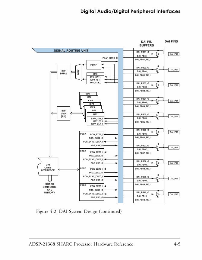
ADSP-21368 SHARC Processor Hardware Reference 4-5
Digital Audio/Digital Peripheral Interfaces
Figure 4-2. DAI System Design (continued)
PDAP
IDP0_CLK_IIDP0_FS_IIDP0_DAT_I
IDP0
IDPDMA[7:1]
IDP1
IDP2
IDP3
IDP4
IDP5
IDP6
PCG_CLKD_O
PCG_EXTD_I
PCG_FSD_O
PCG_CLKC_O
PCG_EXTC_I
PCG_FSC_O
DAICORE
INTERFACE
DAI_P10DAI_PB10_O
DAI_PB10_I
DAI_PB10_PE_I
DAI_P09DAI_PB09_O
DAI_PB09_I
DAI_PB09_PE_I
DAI_P08DAI_PB08_O
DAI_PB08_I
DAI_PB08_PE_I
DAI_P07DAI_PB07_O
DAI_PB07_I
DAI_PB07_PE_I
DAI_P06DAI_PB06_O
DAI_PB06_I
DAI_PB06_PE_I
DAI_P05DAI_PB05_O
DAI_PB05_I
DAI_PB05_PE_I
DAI_P04DAI_PB04_O
DAI_PB04_I
DAI_PB04_PE_I
DAI_P03DAI_PB03_O
DAI_PB03_I
DAI_PB03_PE_I
DAI_P02DAI_PB02_O
DAI_PB02_I
DAI_PB02_PE_I
DAI_P01DAI_PB01_O
DAI_PB01_I
DAI_PB01_PE_I
DAI PINS
SIGNAL ROUTING UNIT
SHARCSIMD CORE
ANDMEMORY
IDP7_DAT_I
IDP7_CLK_IIDP7_FS_I
IDP7
PDAP_STRB_O
IDPDMA0 M
UX
DAI PINBUFFERS
PCG_CLKB_O
PCG_EXTB_I
PCG_FSB_O
PCG_CLKA_O
PCG_EXTA_I
PCG_FSA_O
PCGA
PCGB
PCGC
PCGD
PCG_SYNC_CLKA_I
PCG_SYNC_CLKB_I
PCG_SYNC_CLKC_I
PCG_SYNC_CLKD_I

DAI/DPI System Design
4-6 ADSP-21368 SHARC Processor Hardware Reference
Figure 4-3. DPI System Design
UART0
DPI_P07DPI_PB07_O
DPI_PB07_I
DPI_PB07_PE_I
DPI_P06DPI_PB06_O
DPI_PB06_I
DPI_PB06_PE_I
DPI_P05DPI_PB05_O
DPI_PB05_I
DPI_PB05_PE_I
DPI_P04DPI_PB04_O
DPI_PB04_I
DPI_PB04_PE_I
DPI_P03DPI_PB03_O
DPI_PB03_I
DPI_PB03_PE_I
DPI_P02DPI_PB02_O
DPI_PB02_I
DPI_PB02_PE_I
DPI_P01DPI_PB01_O
DPI_PB01_I
DPI_PB01_PE_I
DPI PINS
TIMER1_O
TIMER1_I
TIMER2_O
GENERALPURPOSECOUNTER/
TIMERS
TIMER3_O
TIMER2_I
TIMER3_I
SIGNAL ROUTING UNIT 2
DPICORE
INTERFACE
DPI PINBUFFERS
UART0_RX_I
UART0_TX_O
UART1
PCG_CLKD_O
PCG_EXTD_I
PCG_FSD_O
PCG_CLKC_O
PCG_EXTC_I
PCG_FSC_O
PCGC
PCGD
PCG_SYNC_CLKC_I
PCG_SYNC_CLKD_I
FLAGS
FLAG[15-4]_PE_O
FLAG[15-4]_O

ADSP-21368 SHARC Processor Hardware Reference 4-7
Digital Audio/Digital Peripheral Interfaces
Figure 4-4. DPI System Design (continued)
DPICORE
INTERFACEDPI_P14
DPI_PB06_O
DPI_PB06_I
DPI_PB06_PE_I
DPI_P13DPI_PB05_O
DPI_PB05_I
DPI_PB05_PE_I
DPI_P12DPI_PB04_O
DPI_PB04_I
DPI_PB04_PE_I
DPI_P11DPI_PB03_O
DPI_PB03_I
DPI_PB03_PE_I
DPI_P09DPI_PB02_O
DPI_PB02_I
DPI_PB02_PE_I
DPI_P08DPI_PB01_O
DPI_PB01_I
DPI_PB01_PE_I
DPI PINS
SIGNAL ROUTING UNIT 2
SHARCSIMD CORE
ANDMEMORY
DPI PINBUFFERS
SPI
TWI
TWI_SDATA_IN
TWI_SCLK_OE
TWI_SDATA_OE
SPI_MOSI_I
SPI_MISO_I
SPI_CLK_I
SPI_DS_I
SPI_FLG0_I
SPI_FLG1_I
SPI_FLG3_I
SPI_FLG2_I
SPI_MOSI_O
SPI_MISO_O
SPI_CLK_O
SPI_DS_O
SPI_FLG0_O
SPI_FLG1_O
SPI_FLG3_O
SPI_FLG2_O
SPI_CLK_PBEN_O
SPIB

Signal Routing Units
4-8 ADSP-21368 SHARC Processor Hardware Reference
Signal Routing UnitsThis section describes how to use the signal routing units (SRU1 and SRU2) to connect inputs to outputs.
Connecting PeripheralsThe SRUs can be likened to a set of patch bays, which contains a bank of inputs and a bank of outputs. For each input, there is a set of permissible output options. Outputs can feed to any number of inputs in parallel, but every input must be patched to exactly one valid output source. Together, the set of inputs and outputs are called a group. The signal’s inputs and outputs that comprise each group all serve similar purposes. They are compatible such that almost any output-to-input patch makes functional sense.
Table 4-2 lists the SRU signal groups that are named sequentially A through F for SRU1 and A through C for SRU2. Each group routes a unique set of signals with a specific purpose. For example, SRU1 Group A routes clock signals, while SRU2 group A routes the external 14 pins and other sources like timer outputs to the inputs of the various peripherals. Unlike SRU1 in the DAI module, all types of functionality like serial clock and data are clubbed into the same group in the DPI/SRU2.
Table 4-2. Pin Signal Group Assignments
Signal Group DAI (SRU1) DPI (SRU2)
Group A Clock routing control Input routing control, includes serial clock and data
Group B Serial data routing control Pin signal assignments
Group C Frame sync routing control Pin enable assignment, routes enables of various peripherals to the drive buffer of each of the 14 pins
Group D Pin signal assignments N/A

ADSP-21368 SHARC Processor Hardware Reference 4-9
Digital Audio/Digital Peripheral Interfaces
Each input and output in each group is given a unique mnemonic. In the few cases where a signal appears in more than one group, the mnemonic is slightly different to distinguish between the connections. The convention is to begin the name with an identifier for the peripheral that the signal is coming to/from followed by the signal’s function as shown in Figure 4-5. A number is included if the DAI contains more than one peripheral type (for example, serial ports) or if the peripheral has more than one signal that performs this function (for example, IDP channels). The mnemonic always ends with _I if the signal is an input, or with _O if the signal is an output.
Note that it is not possible to connect a signal in one group directly to a signal in a different group (analogous to wiring from one patch bay to another). However, group D (in SRU1) is largely devoted to routing in this vein.
Group E Interrupts and miscellaneous signals
N/A
Group F Pin enable signals used to spec-ify whether each DAI pin is used as an output or an input.
N/A
Figure 4-5. Example SRU Mnemonic
Table 4-2. Pin Signal Group Assignments (Cont’d)
Signal Group DAI (SRU1) DPI (SRU2)
SPORT0_CLK_O
PERIPHERAL(SERIAL PORT 0)
SIGNAL’S FUNCTION(CLOCK)
DIRECTION; RELATIVE TOSIGNAL’S PERIPHERAL (OUTPUT)

Signal Routing Units
4-10 ADSP-21368 SHARC Processor Hardware Reference
Pin InterfaceWithin the context of the SRUs, physical connections to the DAI/DPI pins are replaced by a logical interface known as a pin buffer. This is a three-terminal active device capable of sourcing/sinking output current when its driver is enabled, and passing external input signals when dis-abled. Each pin has an input, output, and enable pin as shown in Figure 4-6. The inputs and the outputs are defined with respect to the pin, similar to a peripheral device. This is consistent with the SRU nam-ing convention.
The notation for pin input and output connections can be quite confusing at first because, in a typical system, a pin is simply a wire that connects to a device. The manner in which the pins are connected within the SRU requires additional nomenclature. The pin interface’s input may be thought of as the input to a buffer amplifier that can drive a load on the physical external lead. The pin interface enable is the input signal that enables the output of the buffer by turning it on when its value is logic high, and turning it off when its value is logic low.
Figure 4-6. Pin Buffer Example
IN OUT
ENABLE
PBxx_I
PBxx_O
PBENxx_I
ExternalPackage
ConnectionPin
Interfaceto SRU
PBxx_OPIN
BUFFER

ADSP-21368 SHARC Processor Hardware Reference 4-11
Digital Audio/Digital Peripheral Interfaces
When the pin enable is asserted, the pin output is logically equal to pin input, and the pin is driven. When the pin enable is deasserted, the output of the buffer amplifier becomes high impedance. In this situation, an external device may drive a level onto the line, and the pin is used as an input to the ADSP-21367/8/9 and ADSP-2137x processors.
While the pin is at high impedance and another device is driving a logic level onto the external pin, this logic level value is sent to the SRUs as the pin interface output. Even though the signal is an input to the SHARC processor, it is an output from the pin interface (as a three-terminal device) and may be patched to the signal inputs of peripherals within the SRUs. Pin output is equal to pin input when the pin enable is asserted, but pin output is equal to the external (input) signal when the pin enable is deasserted.
If a DAI/DPI pin is not being used, the pin enable (for example DAI_PBxx_I) for its pin buffer should be connected to LOW and its associated bit in the DAI_PIN_PULLUP register should be set (= 1) to enable a 22.5 kΩ pull-up resistor for that pin.
Pin Buffers as Signal Output PinsIn a typical embedded system, most pins are designated as either inputs or outputs when the circuit is designed, even though they may have the abil-ity to be used in either direction. Each of the DAI/DPI pins can be used as either an input or an output. Although the direction of a DAI/DPI pin is set simply by writing to a memory-mapped register, most often the pin’s direction is dictated by the designated use of that pin. For example, if a DAI pin is hard wired to only the input of another interconnected circuit, it would not make sense for the corresponding pin buffer to be configured as an input. Input pins are commonly tied to logic high or logic low to set the input to a fixed value. Similarly, setting the direction of a DAI pin at system startup by tying the pin buffer enable to a fixed value (either logic high or logic low) is often the simplest and cleanest way to configure the SRUs.

Signal Routing Units
4-12 ADSP-21368 SHARC Processor Hardware Reference
When the DAI/DPI pin is used only as an output, connect the corre-sponding pin buffer enable to logic high as shown in Figure 4-7. This enables the buffer amplifier to operate as a current source and to drive the value present at the pin buffer input onto the DAI/DPI pin and off chip. When the pin buffer enable (in this example PBENxx_I) is set (= 1), the pin buffer output (PBxx_O) is the same signal as the pin buffer input (PBxx_I), and this signal is driven as an output.
Pin Buffers as Signal Input PinsWhen the DAI/DPI pin is used only as an input, connect the correspond-ing pin buffer enable to logic low as shown in Figure 4-8. This disables the buffer amplifier and allows an off-chip source to drive the value present on the DAI/DPI pin and at the pin buffer output. When the pin buffer enable (PBENxx_I) is cleared (= 0), the pin buffer output (PBxx_O) is the signal driven onto the DAI pin by an external source, and the pin buffer input (PBxx_I) is not used.
Figure 4-7. Pin Buffer as Output
IN OUTPIN
ENABLE
DAI_PBxx_I
DAI_PBxx_O
PBENxx_I
EXTERNALPACKAGE
CONNECTIONPIN
INTERFACETO SRU
PADDRIVER
PIN BUFFEROUTPUT
PIN BUFFERINPUT
PIN BUFFERENABLE(= HIGH)
DAI_PBxx_O

ADSP-21368 SHARC Processor Hardware Reference 4-13
Digital Audio/Digital Peripheral Interfaces
Although not strictly necessary, it is recommended programming practice to tie the pin buffer input to logic low whenever the pin buffer enable is tied to logic low. By default, the pin buffer enables are connected to SPORT pin enable signals that may change value. Tying the pin buffer input low decouples the line from irrelevant signals and can make code easier to debug. It also ensures that no voltage is driven by the pin if a bug in your code accidentally asserts the pin enable.
Bidirectional Pin BuffersAll peripherals within the DAI and DPI that have bidirectional pins gen-erate a corresponding pin enable signal. Typically, the settings within a peripheral’s control registers determine if a bidirectional pin is an input or an output, and is then driven accordingly. Both the peripheral control reg-isters and the configuration of the SRUs can effect the direction of signal flow in a pin buffer.
Figure 4-8. Pin Buffer as Input
IN OUTPIN
ENABLE
DAI_PBxx_I
DAI_PBxx_O
PBENxx_I
EXTERNALPACKAGE
CONNECTIONPIN
INTERFACETO SRU
PADDRIVER
PIN BUFFEROUTPUT
PIN BUFFERINPUT
(NOT USED)
PIN BUFFERENABLE(= LOW)
DAI_PBxx_O
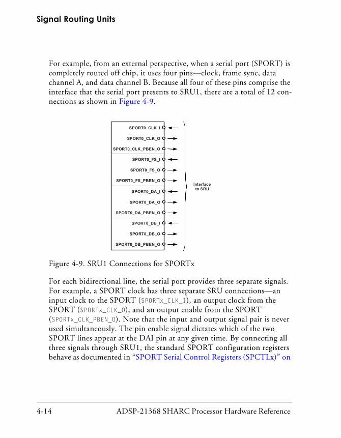
Signal Routing Units
4-14 ADSP-21368 SHARC Processor Hardware Reference
For example, from an external perspective, when a serial port (SPORT) is completely routed off chip, it uses four pins—clock, frame sync, data channel A, and data channel B. Because all four of these pins comprise the interface that the serial port presents to SRU1, there are a total of 12 con-nections as shown in Figure 4-9.
For each bidirectional line, the serial port provides three separate signals. For example, a SPORT clock has three separate SRU connections—an input clock to the SPORT (SPORTx_CLK_I), an output clock from the SPORT (SPORTx_CLK_O), and an output enable from the SPORT (SPORTx_CLK_PBEN_O). Note that the input and output signal pair is never used simultaneously. The pin enable signal dictates which of the two SPORT lines appear at the DAI pin at any given time. By connecting all three signals through SRU1, the standard SPORT configuration registers behave as documented in “SPORT Serial Control Registers (SPCTLx)” on
Figure 4-9. SRU1 Connections for SPORTx
Interfaceto SRU
SPORT0_DA_O
SPORT0_DA_I
SPORT0_DA_PBEN_O
SPORT0_FS_O
SPORT0_FS_I
SPORT0_FS_PBEN_O
SPORT0_CLK_O
SPORT0_CLK_I
SPORT0_CLK_PBEN_O
SPORT0_DB_O
SPORT0_DB_I
SPORT0_DB_PBEN_O

ADSP-21368 SHARC Processor Hardware Reference 4-15
Digital Audio/Digital Peripheral Interfaces
page A-29. SRU1 then becomes transparent to the peripheral. Figure 4-10 demonstrates SPORT0 properly routed to DAI pins one through four—although it can be equally well routed to any of the 20 DAI pins.
Though SPORT signals are capable of operating in this bidirectional man-ner, it is not required that they be connected to the pin buffer this way. As mentioned above, if the system design only uses a SPORT signal in one direction, it is easier and safer to connect the pin buffer enable directly high or low as appropriate. Furthermore, signals in the SRUs other than the pin buffer enable signal (which is generated by the peripheral) may be routed to the pin buffer enable input. For example, an outside source may be used to ‘gate’ a pin buffer output by controlling the corresponding pin buffer enable.
Making Connections in the SRUsAs described previously, the SRUs are similar to a set of patch bays. Each bay routes a distinct set of outputs to compatible inputs. These connec-tions are implemented as a set of memory-mapped registers with a bit field for each input. The outputs are implemented as a set of bit encodings. Conceptually, a patch cord is used to connect an output to an input. In the SRUs, a bit pattern that is associated with a signal output (shown as item 1 in Figure 4-11) is written to a bit field corresponding to a signal input (shown as item 2 in Figure 4-11).
The memory-mapped SRU registers are arranged by groups, referred to as group A through group F in SRU1 and group A through group C in SRU2 and described in “DAI/SRU1 Connection Groups” on page 4-18 and “DPI/SRU2 Connection Groups” on page 4-51. Each group has a unique encoding for its associated output signals and a set of configura-tion registers. For example, in the DAI, group A is used to route clock signals. Five memory-mapped registers, SRU_CLK4–0, contain 5-bit wide fields corresponding to the clock inputs of various peripherals. The values written to these bit fields specify a signal source that is an output from

Making Connections in the SRUs
4-16 ADSP-21368 SHARC Processor Hardware Reference
Figure 4-10. SRU1 Connection to Four Bidirectional SPORT Pins
SPORT0_DA_O
SPORT0_DA_I
SPORT0_DA_PBEN_O
SPORT0_FS_O
SPORT0_FS_I
SPORT0_FS_PBEN_O
SPORT0_CLK_O
SPORT0_CLK_I
SPORT0_CLK_PBEN_O
SPORT0_DB_O
SPORT0_DB_I
SPORT0_DB_PBEN_O
PINENABLE
PB01_I
PB01_O
PBEN01_I
PB01_OIN OUT
EXTERNALPACKAGE
CONNECTION
PINENABLE
PB02_I
PB02_O
PBEN02_I
PB02_OIN OUT
PINENABLE
PB03_I
PB03_O
PBEN03_I
PB03_OIN OUT
PINENABLE
PB04_I
PB04_O
PBEN04_I
PB04_OIN OUT
EXTERNALPACKAGE
CONNECTION
EXTERNALPACKAGE
CONNECTION
EXTERNALPACKAGE
CONNECTION

ADSP-21368 SHARC Processor Hardware Reference 4-17
Digital Audio/Digital Peripheral Interfaces
another peripheral. All of the possible encodings represent sources that are clock signals (or at least could be clock signals in some systems). Figure 4-11 diagrams the input signals that are controlled by the DAI group A register, SRU_CLK0. All bit fields in the SRU1 configuration regis-ters correspond to inputs. The value written to the bit field specifies the signal source. This value is also an output from some other component within the SRU.
Note that the lower portion of the patch bay in Figure 4-11 is shown with a large number of ports to reinforce the point that one output can be con-nected to many inputs. The same encoding can be written to any number of bit fields in the same group. It is not possible to run out of patch points for an output signal.
Figure 4-11. Patching to the Group A Register SRU_CLK0
2 SRU: GROUP ASRU_CLK0
SPORT5_CLK_I(11001)
SPORT4_CLK_I(11000)
SPORT3_CLK_I(10111)
SPORT0_CLK_I(10100)
SPORT1_CLK_I(10101)
SPORT2_CLK_I(10110)
4:09:514:1019:1524:2029:25
1

Making Connections in the SRUs
4-18 ADSP-21368 SHARC Processor Hardware Reference
Just as DAI group A routes clock signals, each of the other groups route a collection of compatible signals. Group B routes serial data streams while group C routes frame sync signals. Group D routes signals to pins so that they may be driven off chip. Note that all of the groups have an encoding that allows a signal to flow from a pin output to the input being specified by the bit field. However, group D is required to route a signal to the pin input. Group F routes signals to the pin enables, and the value of these signals determines if a DAI pin is used as an output or an input. These groups are described in more detail in the following sections.
DAI/SRU1 Connection GroupsThe DAI/SRU1 has the default configuration shown in Table 4-3.
There are five separate groups of connections that are used in SRU1. The following sections summarize each.
Table 4-3. DAI/SRU1 Default Configuration
Pin Number Signal Name Pin Number Signal Name
DAI_01 SPORT0_DA DAI_11 SPORT3_DA
DAI_02 SPORT0_DB DAI_12 SPORT3_DB
DAI_03 SPORT0_CLK DAI_13 SPORT3_CLK
DAI_04 SPORT0_FS DAI_14 SPORT3_FS
DAI_05 SPORT1_DA DAI_15 SPORT4_DA
DAI_06 SPORT1_DB DAI_16 SPORT4_DB
DAI_07 SPORT1_CLK DAI_17 SPORT5_DA
DAI_08 SPORT1_FS DAI_18 SPORT5_DB
DAI_09 SPORT2_DA DAI_19 SPORT5_CLK
DAI_10 SPORT2_DB DAI_20 SPORT5_FS

ADSP-21368 SHARC Processor Hardware Reference 4-19
Digital Audio/Digital Peripheral Interfaces
Group A Connections—Clock Signals
Group A is used to route the following signals to clock inputs and are selected from the list of group A sources.
• SPORTs clock inputs (when the SPORTs are in clock slave mode)
• Clock inputs to the eight IDP (input data port) channels
• Four precision clock generator (PCG) external sources
• SRC clock inputs
• SPDIF transmitter clock inputs
When channel 0 of the IDP is configured for PDAP input, the clock source set here is used as the parallel word latch instead of the serial bit clock.
Set all clock inputs that are not used to logic low. Any IDP channels that receive clock signals as set here send data to the FIFO. When a SPORT is used as a clock master, setting the unused SPORT clock input to logic low improves signal integrity. The registers are shown in Figure 4-12 through Figure 4-17. The input and output signals for group A are summarized in Table 4-4 on page 4-23.
The following notes apply to the group A connections
1. The SRU_CLK4–0 registers are 30-bit registers. On reads, bits 30 and 31 always return zero.
2. SPORTs 6 and 7 receive their clocks from other sources but cannot send their own clocks to other SPORTs or other peripherals internally through SRU. If needed, they have to be connected externally through pins.

Making Connections in the SRUs
4-20 ADSP-21368 SHARC Processor Hardware Reference
3. Setting SRU_CLK4[4:0] = 0x1C connects PCG_EXTA_I to logic low, not PCG_CLKA_O. Setting SRU_CLK4[9:5] = 0x1D connects PCG_EXTB_I to logic low, not PCG_CLKB_O.
Figure 4-12. SRU_CLK0 Register
31 30 29 28 27 26 25 24 23 22 21 20 19 18 17 16
00 0 1 0 0 1 0 1 0 0 1 0 0 1 1
Reserved
15 14 13 12 11 10 9 8 7 6 5 4 3 2 1 0
00 0 1 1 0 0 0 0 1 1 0 0 0 0 1
SPORT5_CLK_ISerial Port 5 Clock Input
SPORT3_CLK_ISerial Port 3 Clock Input
SPORT4_CLK_ISerial Port 4 Clock Input
SPORT2_CLK_ISerial Port 2 Clock Input SPORT1_CLK_I
Serial Port 1 Clock Input
SPORT0_CLK_I
Serial Port 0 Clock Input
SRU_CLK0 (0x2430)
SPORT3_CLK_I
Reset = 0x252630C2

ADSP-21368 SHARC Processor Hardware Reference 4-21
Digital Audio/Digital Peripheral Interfaces
Figure 4-13. SRU_CLK1 Register
Figure 4-14. SRU_CLK2 Register
31 30 29 28 27 26 25 24 23 22 21 20 19 18 17 16
10 0 1 1 1 1 0 1 1 1 1 0 1 1 1
Reserved
Reset = 0x3DEF7BDE
15 14 13 12 11 10 9 8 7 6 5 4 3 2 1 0
00 1 1 1 1 0 1 1 1 1 0 1 1 1 1
SRC2_CLK_OP_I
SRC1_CLK_OP_I
SRC2_CLK_IP_I
SRU_CLK1 (0x2431)
SRC1_CLK_OP_I
SRC1_CLK_IP_ISRC0_CLK_OP_I
SRC0_CLK_IP_I
Sample Rate Converter 2 Clock Output Input
Sample Rate Converter 1 Clock Output Input
Sample Rate Converter 2 Clock Input Input
Sample Rate Converter 1 Clock Output Input Sample Rate Converter 0
Clock Input Input
Sample Rate Converter 0 Clock Output Input
Sample Rate Converter 1 Clock Input Input
31 30 29 28 27 26 25 24 23 22 21 20 19 18 17 16
10 0 1 1 1 1 0 1 1 1 1 0 1 1 1
Reserved
15 14 13 12 11 10 9 8 7 6 5 4 3 2 1 0
00 1 1 1 1 0 1 1 1 1 0 1 1 1 1
IDP2_CLK_IInput Data Port 2 Clock Input
IDP0_CLK_IInput Data Port 0 Clock Input
DIT_CLK_I
SRC3_CLK_IP_I
SRC3_CLK_OP_I
SRU_CLK2 (0x2432)
IDP0_CLK_I
Reset = 0x3DEF7BDE
IDP1_CLK_IInput Data Port 1Clock Input
Sample Rate Converter 3 Clock Input Input
SPDIF Transmitter Clock Input Sample Rate Converter 3
Clock Output Input
Input Data Port 0 Clock Input

Making Connections in the SRUs
4-22 ADSP-21368 SHARC Processor Hardware Reference
Figure 4-15. SRU_CLK3 Register
Figure 4-16. SRU_CLK4 Register
31 30 29 28 27 26 25 24 23 22 21 20 19 18 17 16
10 0 1 1 1 1 0 1 1 1 1 0 1 1 1
Reserved
15 14 13 12 11 10 9 8 7 6 5 4 3 2 1 0
00 1 1 1 1 0 1 1 1 1 0 1 1 1 1
SRU_CLK3 (0x2433) Reset = 0x3DEF7BDE
DIT_HFCLK_I
IDP6_CLK_I
IDP7_CLK_I
IDP6_CLK_I
IDP5_CLK_I
IDP3_CLK_I
IDP4_CLK_I
Input Data Port Channel 6 Clock Input
SPDIF Oversampling Clock Input
Input Data Port Channel 3 Clock Input
Input Data Port Channel 4 Clock Input
Input Data Port Channel 7 Clock Input
Input Data Port Channel 5 Clock Input
Input Data Port Channel 6 Clock Input
31 30 29 28 27 26 25 24 23 22 21 20 19 18 17 16
10 0 1 1 1 1 0 1 1 1 1 0 1 1 1
Reserved
15 14 13 12 11 10 9 8 7 6 5 4 3 2 1 0
00 1 1 1 1 0 1 1 1 1 0 1 1 1 1
SPDIF_EXTPLLCLK_I
External 512 x FS PLL Clock Input
PCG_EXTA_I
Precision Clock Generator External Clock A Input
PCG_EXTB_I
Precision Clock Generator External Clock B Input
SRU_CLK4 (0x2434)
Setting SRU_CLK4 4–0 = 28 connects PCG_EXTA_I to logic low, not to PCG_CLKA_O.Setting SRU_CLK4 9–5 = 29 connects PCG_EXTB_I to logic low, not to PCG_CLKB_O.
PCG_SYNC_CLKB_IPrecision Clock Generator Clock B Sync Input
Reserved
PCG_SYNC_CLKA_I
Precision Clock Generator Clock A Sync Input
Reset = 0x3DEF7BDE
Reserved

ADSP-21368 SHARC Processor Hardware Reference 4-23
Digital Audio/Digital Peripheral Interfaces
Figure 4-17. SRU_CLK5 Register
Table 4-4. Group A Sources—Serial Clock
Selection Code Source Signal Description (Source)
00000 (0x0) DAI_PB01_O Select DAI pin buffer 1
00001 (0x1) DAI_PB02_O Select DAI pin buffer 2
00010 (0x2) DAI_PB03_O Select DAI pin buffer 3
00011 (0x3) DAI_PB04_O Select DAI pin buffer 4
00100 (0x4) DAI_PB05_O Select DAI pin buffer 5
00101 (0x5) DAI_PB06_O Select DAI pin buffer 6
00110 (0x6) DAI_PB07_O Select DAI pin buffer 7
00111 (0x7) DAI_PB08_O Select DAI pin buffer 8
01000 (0x8) DAI_PB09_O Select DAI pin buffer 9
01001 (0x9) DAI_PB10_O Select DAI pin buffer 10
01010 (0xA) DAI_PB11_O Select DAI pin buffer 11
31 30 29 28 27 26 25 24 23 22 21 20 19 18 17 16
10 0 1 1 1 1 0 1 1 1 1 0 1 1 1
Reserved
15 14 13 12 11 10 9 8 7 6 5 4 3 2 1 0
00 1 1 1 1 0 1 1 1 1 0 1 1 1 1
PCG_SYNC_CLKC_I
Precision Clock Generator Clock C Sync Input
SPORT6_CLK_I
Serial Port 6 Clock Input
SPORT7_CLK_I
Serial Port 7 Clock Input
SRU_CLK5 (0x2435)
PCG_SYNC_CLKD_I
Precision Clock Generator Clock D Sync Input
PCG_EXTC_I
Reset = 0x3DEF7BDE
PCG_SYNC_CLKD_I
Precision Clock Generator External Clock C Input
PCG_EXTD_I
Precision Clock Generator External Clock D Input
Precision Clock Generator Clock D Sync Input

Making Connections in the SRUs
4-24 ADSP-21368 SHARC Processor Hardware Reference
01011 (0xB) DAI_PB12_O Select DAI pin buffer 12
01100 (0xC) DAI_PB13_O Select DAI pin buffer 13
01101 (0xD) DAI_PB14_O Select DAI pin buffer 14
01110 (0xE) DAI_PB15_O Select DAI pin buffer 15
01111 (0xF) DAI_PB16_O Select DAI pin buffer 16
10000 (0x10) DAI_PB17_O Select DAI pin buffer 17
10001 (0x11) DAI_PB18_O Select DAI pin buffer 18
10010 (0x12) DAI_PB19_O Select DAI pin buffer 19
10011 (0x13) DAI_PB20_O Select DAI pin buffer 20
10100 (0x14) SPORT0_CLK_O Select SPORT 0 Clock
10101 (0x15) SPORT1_CLK_O Select SPORT 1 Clock
10110 (0x16) SPORT2_CLK_O Select SPORT 2 Clock
10111 (0x17) SPORT3_CLK_O Select SPORT 3 Clock
11000 (0x18) SPORT4_CLK_O Select SPORT 4 Clock
11001 (0x19) SPORT5_CLK_O Select SPORT 5 Clock
11010 (0x1A) DIR_CLK_O Select SPDIF receive clock output
11011 (0x1B) DIR_TDMCLK_O Select SPDIF receive TDM clock output
11100 (0x1C) PCG_CLKA_O Select precision clock A output
11101 (0x1D) PCG_CLKB_O Select precision clock B output
11110 (0x1E) LOW Select logic level low (0)
11111 (0x1F) HIGH Select logic level high (1)
Table 4-4. Group A Sources—Serial Clock (Cont’d)
Selection Code Source Signal Description (Source)

ADSP-21368 SHARC Processor Hardware Reference 4-25
Digital Audio/Digital Peripheral Interfaces
Group B Connections—Data Signals
Group B connections are used to route signals to serial data inputs. This includes serial data inputs to both the A and B channels of the SPORTs and to each of the eight IDP channels. The SRCs and SPDIF transmitter are also selected from the list of group B sources and set in the group B registers. When a SPORT is configured to transmit, the data source set here is ignored. Likewise, when channel 0 of the IDP is used for the PDAP, the serial data source set here is ignored. The registers are shown in Figure 4-18 through Figure 4-24. The input and output signals for group B are summarized in Table 4-5 on page 4-29.
The following notes apply to group B connections.
1. SRU_DAT0, SRU_DAT1, SRU_DAT2, SRU_DAT3, SRU_DAT4, and SRU_DAT5 are 30-bit registers. On reads, bits 30 and 31 always return zero.
2. SRU_DAT6 is a 24-bit register. On reads, bits 31 through 24 always return zero.
Figure 4-18. SRU_DAT0 Register
31 30 29 28 27 26 25 24 23 22 21 20 19 18 17 16
00 0 0 0 1 0 0 0 0 0 0 1 0 1 0
Reserved
15 14 13 12 11 10 9 8 7 6 5 4 3 2 1 0
00 1 0 0 0 0 0 0 0 1 0 0 0 0 0
Serial Port 2 Data Channel A Input
SPORT2_DA_ISerial Port 1 DataChannel A Input
SPORT1_DA_I
Serial Port 1 Data Channel B Input
SPORT1_DB_I
Serial Port 0 Data Channel B Input
SPORT0_DB_I Serial Port 0 DataChannel A Input
SPORT0_DA_I
SRU_DAT0 (0x2440)
SPORT1_DA_I
Reset = 0x08144040
Serial Port 1 Data Channel A Input

Making Connections in the SRUs
4-26 ADSP-21368 SHARC Processor Hardware Reference
Figure 4-19. SRU_DAT1 Register
Figure 4-20. SRU_DAT2 Register
31 30 29 28 27 26 25 24 23 22 21 20 19 18 17 16
00 0 0 0 1 1 1 1 0 0 1 1 1 0 0
Reserved
15 14 13 12 11 10 9 8 7 6 5 4 3 2 1 0
11 0 1 1 0 0 1 0 1 0 0 0 1 0 0
Serial Port 4 Data Channel B Input
SPORT4_DB_ISerial Port 3 Data Channel B Input
SPORT3_DB_I
Serial Port 4 Data Channel A Input
SPORT4_DA_I
Serial Port 3 Data Channel A Input
SPORT3_DA_I Serial Port 2 DataChannel B Input
SPORT2_DB_I
SRU_DAT1 (0x2441)
SPORT3_DB_I
Reset = 0x0F38B289
Serial Port 3 Data Channel B Input
Reserved
15 14 13 12 11 10 9 8 7 6 5 4 3 2 1 0
00 0 0 0 0 1 0 0 0 1 0 1 0 0 0
Serial Port 5 Data Channel B Input
SPORT5_DB_ISerial Port 5 DataChannel A Input
SPORT5_DA_I
SRU_DAT2 (0x2442)
SRC0_DAT_IP_I
Reset = 0x00000450
Sample Rate Converter 2 Data Input Input
SRC2_DAT_IP_I
Sample Rate Converter 1 Data Input Input
SRC1_DAT_IP_I
Sample Rate Converter 0 Data Input Input
31 30 29 28 27 26 25 24 23 22 21 20 19 18 17 16
00 0 0 0 0 0 0 0 0 0 0 0 0 0 0
SRC0_DAT_IP_ISample Rate Converter 0 Data Input Input

ADSP-21368 SHARC Processor Hardware Reference 4-27
Digital Audio/Digital Peripheral Interfaces
Figure 4-21. SRU_DAT3 Register
Figure 4-22. SRU_DAT4 Register
31 30 29 28 27 26 25 24 23 22 21 20 19 18 17 16
00 0 0 0 0 0 0 0 0 0 0 0 0 0 0
Reserved
15 14 13 12 11 10 9 8 7 6 5 4 3 2 1 0
00 0 0 0 0 0 0 0 0 0 0 0 0 0 0
Sample Rate Converter 3 TDM Output Input
SRC3_TDM_OP_I
SRC1_TDM_OP_I
SRC2_TDM_OP_I
SRC0_TDM_OP_I
SRU_DAT3 (0x2443) Reset = 0x00000000
SRC3_DAT_IP_I
Sample Rate Converter 2 TDM Output Input
Sample Rate Converter 1 TDM Output Input
Sample Rate Converter 0 TDM Output Input
Sample Rate Converter 3 Data Input Input
SRC1_TDM_OP_ISample Rate Converter 1 TDM Output Input
31 30 29 28 27 26 25 24 23 22 21 20 19 18 17 16
00 0 0 0 0 0 0 0 0 0 0 0 0 0 0
Reserved
15 14 13 12 11 10 9 8 7 6 5 4 3 2 1 0
00 0 0 0 0 0 0 0 0 0 0 0 0 0 0
SPDIF Transmit Data Input
DIT_DAT_I
IDP2_DAT_IInput Data Port 2 Data Input
IDP3_DAT_I
Input Data Port 3 Data Input
IDP0_DAT_IInput Data Port 0 Data Input
SRU_DAT4 (0x2444)
IDP1_DAT_I
Reset = 0x00000000
Input Data Port 1 Data Input
IDP1_DAT_IInput Data Port 1 Data Input

Making Connections in the SRUs
4-28 ADSP-21368 SHARC Processor Hardware Reference
Figure 4-23. SRU_DAT5 Register
Figure 4-24. SRU_DAT6 Register
31 30 29 28 27 26 25 24 23 22 21 20 19 18 17 16
00 0 0 0 0 0 0 0 0 0 0 0 0 0 0
15 14 13 12 11 10 9 8 7 6 5 4 3 2 1 0
00 0 0 0 0 0 0 0 0 0 0 0 0 0 0
Input Data Port 4 DataChannel A Input
IDP4_DAT_I
IDP6_DAT_I
IDP7_DAT_I
Input Data Port 7 Data Input
IDP5_DAT_I
Input Data Port 5 Data Input
SRU_DAT5 (0x2445)
IDP6_DAT_I
Reset = 0x00000000
Input Data Port 6 Data Input
SPDIF Receive Data Input
DIR_DAT_I Input Data Port 6 Data Input
31 30 29 28 27 26 25 24 23 22 21 20 19 18 17 16
00 0 0 0 0 0 0 0 0 0 0 0 0 0 0
Reserved
15 14 13 12 11 10 9 8 7 6 5 4 3 2 1 0
00 0 0 0 0 0 0 0 0 0 0 0 0 0 0
Serial Port 7 Data Channel A Input
SPORT7_DA_I
Serial Port 7 Data Channel BA Input
SPORT7_DB_I
Serial Port 6 Data Channel B Input
SPORT6_DB_I Serial Port 6 DataChannel A Input
SPORT6_DA_I
SRU_DAT6 (0x2446)
SPORT7_DA_I
Reset = 0x00000000
Serial Port 7 Data Channel A Input

ADSP-21368 SHARC Processor Hardware Reference 4-29
Digital Audio/Digital Peripheral Interfaces
Table 4-5. Group B Sources—Serial Data
Selection Code Source Signal Description (Source)
000000 (0x0) DAI_PB01_O Select DAI pin buffer 1
000001 (0x1) DAI_PB02_O Select DAI pin buffer 2
000010 (0x2) DAI_PB03_O Select DAI pin buffer 3
000011 (0x3) DAI_PB04_O Select DAI pin buffer 4
000100 (0x4) DAI_PB05_O Select DAI pin buffer 5
000101 (0x5) DAI_PB06_O Select DAI pin buffer 6
000110 (0x6) DAI_PB07_O Select DAI pin buffer 7
000111 (0x7) DAI_PB08_O Select DAI pin buffer 8
001000 (0x8) DAI_PB09_O Select DAI pin buffer 9
001001 (0x9) DAI_PB10_O Select DAI pin buffer 10
001010 (0xA) DAI_PB11_O Select DAI pin buffer 11
001011 (0xB) DAI_PB12_O Select DAI pin buffer 12
001100 (0xC) DAI_PB13_O Select DAI pin buffer 13
001101 (0xD) DAI_PB14_O Select DAI pin buffer 14
001110 (0xE) DAI_PB15_O Select DAI pin buffer 15
001111 (0xF) DAI_PB16_O Select DAI pin buffer 16
010000 (0x10) DAI_PB17_O Select DAI pin buffer 17
010001 (0x11) DAI_PB18_O Select DAI pin buffer 18
010010 (0x12) DAI_PB19_O Select DAI pin buffer 19
010011 (0x13) DAI_PB20_O Select DAI pin buffer 20
010100 (0x14) SPORT0_DA_O Select SPORT 0A data
010101 (0x15) SPORT0_DB_O Select SPORT 0B data
010110 (0x16) SPORT1_DA_O Select SPORT 1A data
010111 (0x17) SPORT1_DB_O Select SPORT 1B data

Making Connections in the SRUs
4-30 ADSP-21368 SHARC Processor Hardware Reference
011000 (0x18) SPORT2_DA_O Select SPORT 2A data
011001 (0x19) SPORT2_DB_O Select SPORT 2B data
011010 (0x1A) SPORT3_DA_O Select SPORT 3A data
011011 (0x1B) SPORT3_DB_O Select SPORT 3B data
011100 (0x1C) SPORT4_DA_O Select SPORT 4A data
011101 (0x1D) SPORT4_DB_O Select SPORT 4B data
011110 (0x1E) SPORT5_DA_O Select SPORT 5A data
011111 (0x1F) SPORT5_DB_O Select SPORT 5B data
100000 (0x20) SRC0_DAT_OP_O SRC0 data out (stereo)
100001 (0x21) SRC1_DAT_OP_O SRC1 data out (stereo)
100010 (0x22) SRC2_DAT_OP_O SRC2 data out (stereo)
100011 (0x23) SRC3_DAT_OP_O SRC3 data out (stereo)
100100 (0x24) SRC0_TDM_IP_O SRC0 data out
100101 (0x25) SRC1_TDM_IP_O SRC1 data out
100110 (0x26) SRC2_TDM_IP_O SRC2 data out
100111 (0x27) SRC3_TDM_IP_O SRC3 data out
101000 (0x28) DIR_DAT_O SPDIF_RX serial data out
101001 (0x29) LOW Select logic level low (0)
101010 (0x2A) LOW Select logic level low (0)
101011 (0x2B) HIGH Select logic level high (1)
101100 (0x2C) SPORT6_DA_O Select SPORT 6A data
101101 (0x2D) SPORT6_DB_O Select SPORT 6B data
101110 (0x2E) SPORT7_DA_O Select SPORT 7A data
101111 (0x2F) SPORT7_DB_O Select SPORT 7B data
Table 4-5. Group B Sources—Serial Data (Cont’d)
Selection Code Source Signal Description (Source)

ADSP-21368 SHARC Processor Hardware Reference 4-31
Digital Audio/Digital Peripheral Interfaces
Group C Connections—Frame Sync Signals
Group C connections are used to route signals to frame sync inputs. These are the SPORT frame sync inputs (when the SPORT is in slave mode) and the frame sync inputs to the eight IDP channels. The SRCs and SPDIF transmitter and receiver are also selected from the list of group C sources and set in the group C registers.
Each of the frame sync inputs specified is connected to a frame sync source based on the 5-bit values described in the group C frame sync sources. Thirty-two possible frame sync sources can be connected using the SRU_FS0-4 registers. The registers are shown in Figure 4-25 through Figure 4-29. The input and output signals for group C are summarized in Table 4-6 on page 4-35.
The following notes apply to group C connections.
1. SRU_FS0, SRU_FS1, and SRU_FS2 are 30-bit registers. On reads, bits 30 and 31 always return zero.
2. SRU_FS3 is a 24-bit register. On reads, bits 31 through 24 always return zero.
3. SRU_FS4 is a 10-bit register. On reads, bits 31 through 10 always return zero.
110000 (0x30) DIT_O Select SPDIF biphase encoded output
110001 (0x31) –111101 (0x3D) Reserved
111110 (0x3E) LOW Select logic level low (0)
111111 (0x3F) HIGH Select logic level high (1)
Table 4-5. Group B Sources—Serial Data (Cont’d)
Selection Code Source Signal Description (Source)

Making Connections in the SRUs
4-32 ADSP-21368 SHARC Processor Hardware Reference
4. SPORTs 6 and 7 receive frame syncs from other sources but cannot send their own frame syncs to other SPORTs or other peripherals internally through the SRU. If needed, they have to be connected externally through pins.
Figure 4-25. SRU_FS0 Register
31 30 29 28 27 26 25 24 23 22 21 20 19 18 17 16
00 0 1 0 0 1 1 1 0 0 1 1 0 1 1
Reserved
15 14 13 12 11 10 9 8 7 6 5 4 3 2 1 0
11 0 1 1 0 1 0 0 1 1 1 0 0 0 1
Serial Port 2 Frame Sync Input
SPORT2_FS_ISerial Port 0 Frame Sync Input
SPORT0_FS_I
Serial Port 5 Frame Sync Input
SPORT5_FS_I
Serial Port 3 Frame Sync Input
SPORT3_FS_I
Serial Port 4 Frame Sync Input
SPORT4_FS_I
Serial Port 1 Frame Sync Input
SPORT1_FS_I
SRU_FS0 (0x2450)
SPORT3_FS_I
Serial Port 3 Frame Sync Input
Reset = 0x2736B4E3

ADSP-21368 SHARC Processor Hardware Reference 4-33
Digital Audio/Digital Peripheral Interfaces
Figure 4-26. SRU_FS1 Register
Figure 4-27. SRU_FS2 Register
31 30 29 28 27 26 25 24 23 22 21 20 19 18 17 16
10 0 1 1 1 1 0 1 1 1 1 0 1 1 1
Reserved
15 14 13 12 11 10 9 8 7 6 5 4 3 2 1 0
00 1 1 1 1 0 1 1 1 1 0 1 1 1 1
SRC2_FS_OP_I
SRC1_FS_OP_I
SRC2_FS_IP_I
SRU_FS1 (0x2451)
SRC1_FS_OP_ISRC0_FS_IP_I
SRC0_FS_OP_ISRC1_FS_IP_I
Sample Rate Converter 2 Frame Sync Output Input Sample Rate Converter 2
Frame Sync Input Input
Sample Rate Converter 0 Frame Sync Input Input
Sample Rate Converter 1 Frame Sync Output Input
Sample Rate Converter 1 Frame Sync Input Input Sample Rate Converter 0
Frame Sync Output Input
Sample Rate Converter 1 Frame Sync Output Input
Reset = 0x3DEF7BDE
31 30 29 28 27 26 25 24 23 22 21 20 19 18 17 16
10 0 1 1 1 1 0 1 1 1 1 0 1 1 1
Reserved
15 14 13 12 11 10 9 8 7 6 5 4 3 2 1 0
00 1 1 1 1 0 1 1 1 1 0 1 1 1 1
IDP2_FS_I
SPDIF_TX_FS_I
IDP0_FS_I
SRU_FS2 (0x2452)
IDP0_FS_ISRC3_FS_IP_I
SRC3_FS_OP_I
IDP1_FS_I
Sample Rate Converter 3 Frame Sync Input Input
Input Data Port Channel 1 Frame Sync Input
Input Data Port Channel 0 Frame Sync Input
Input Data Port Channel 0 Frame Sync Input
Sample Rate Converter 3 Frame Sync Output Input
SPDIF 3 Oversampling Clock Input
Input Data Port Channel 0 Frame Sync Input
Reset = 0x3DEF7BDE

Making Connections in the SRUs
4-34 ADSP-21368 SHARC Processor Hardware Reference
Figure 4-28. SRU_FS3 Register
Figure 4-29. SRU_FS4 Register
31 30 29 28 27 26 25 24 23 22 21 20 19 18 17 16
10 0 1 1 1 1 0 1 1 1 1 0 1 1 1
Reserved
15 14 13 12 11 10 9 8 7 6 5 4 3 2 1 0
00 1 1 1 1 0 1 1 1 1 0 1 1 1 1
Input Data Port Channel 7 Frame Sync Input
IDP7_FS_I
IDP5_FS_I
IDP6_FS_I
Input Data Port Channel 5 Frame Sync Input
IDP4_FS_I
Input Data Port Channel 4 Frame Sync Input
Input Data Port Channel 3 Frame Sync Input
IDP3_FS_I
SRU_FS3 (0x2453)
SPDIF_RX_I
SPDIF Receiver Biphase Encoded Data Input
Input Data Port Channel 6 Frame Sync Input
IDP6_FS_I
Input Data Port Channel 6 Frame Sync Input
Reset = 0x3DEF7BDE
31 30 29 28 27 26 25 24 23 22 21 20 19 18 17 16
00 0 0 0 0 0 0 0 0 0 0 0 0 0 0
15 14 13 12 11 10 9 8 7 6 5 4 3 2 1 0
00 0 0 0 0 0 1 1 1 1 0 1 1 1 1
Serial Port 6 Frame Sync Input
SPORT6_FS_I
Reserved
Serial Port 7 Frame Sync Input
SPORT7_FS_I
SRU_FS4 (0x2454)
Reserved
Reset = 0x000003DE

ADSP-21368 SHARC Processor Hardware Reference 4-35
Digital Audio/Digital Peripheral Interfaces
Table 4-6. Group C Sources—Frame Sync
Selection Code Source Signal Description (Source)
00000 (0x0) DAI_PB01_O Select DAI pin buffer 1
00001 (0x1) DAI_PB02_O Select DAI pin buffer 2
00010 (0x2) DAI_PB03_O Select DAI pin buffer 3
00011 (0x3) DAI_PB04_O Select DAI pin buffer 4
00100 (0x4) DAI_PB05_O Select DAI pin buffer 5
00101 (0x5) DAI_PB06_O Select DAI pin buffer 6
00110 (0x6) DAI_PB07_O Select DAI pin buffer 7
00111 (0x7) DAI_PB08_O Select DAI pin buffer 8
01000 (0x8) DAI_PB09_O Select DAI pin buffer 9
01001 (0x9) DAI_PB10_O Select DAI pin buffer 10
01010 (0xA) DAI_PB11_O Select DAI pin buffer 11
01011 (0xB) DAI_PB12_O Select DAI pin buffer 12
01100 (0xC) DAI_PB13_O Select DAI pin buffer 13
01101 (0xD) DAI_PB14_O Select DAI pin buffer 14
01110 (0xE) DAI_PB15_O Select DAI pin buffer 15
01111 (0xF) DAI_PB16_O Select DAI pin buffer 16
10000 (0x10) DAI_PB17_O Select DAI pin buffer 17
10001 (0x11) DAI_PB18_O Select DAI pin buffer 18
10010 (0x12) DAI_PB19_O Select DAI pin buffer 19
10011 (0x13) DAI_PB20_O Select DAI pin buffer 20
10100 (0x14) SPORT0_FS_O Select SPORT 0 frame sync
10101 (0x15) SPORT1_FS_O Select SPORT 1 frame sync
10110 (0x16) SPORT2_FS_O Select SPORT 2 frame sync
10111 (0x17) SPORT3_FS_O Select SPORT 3 frame sync
Making Connections in the SRUs
4-36 ADSP-21368 SHARC Processor Hardware Reference
Group D Connections—Pin Signal Assignments
Group D is used to specify any signals that are driven off chip by the pin buffers. A pin buffer input (DAI_PBxx_I) is driven as an output from the processor when the pin buffer enable is set (= 1).
Each physical pin (connected to a bonded pad) may be routed via the SRU to any of the outputs of the DAI audio peripherals, based on the 7-bit val-ues listed in Table 4-7 on page 4-39. The SRU may also be used to route signals that control the pins in other ways. These signals may be config-ured for use as general-purpose I/O, precision clock generators, or miscellaneous control signals. The registers are shown in Figure 4-30 through Figure 4-34.
The following notes apply to the group D sources.
1. Setting SRU_PIN4[28] to high inverts the level of DAI_P19_I and setting SRU_PIN4[29] inverts the level of DAI_P20_I.
2. If SRU_PIN4[20:14] = 0x12 then setting SRU_PIN4[28] to high does not invert the output.
11000 (0x18) SPORT4_FS_O Select SPORT 4 frame sync
11001 (0x19) SPORT5_FS_O Select SPORT 5 frame sync
11010 (0x1A) DIR_FS_O SPDIF_RX frame sync output
11011 (0x1B) Reserved
11100 (0x1C) PCG_FSA_O Select precision frame sync A output
11101 (0x1D) PCG_FSB_O Select precision frame sync B output
11110 (0x1E) LOW Select logic level low (0)
11111 (0x1F) HIGH Select logic level high (1)
Table 4-6. Group C Sources—Frame Sync (Cont’d)
Selection Code Source Signal Description (Source)

ADSP-21368 SHARC Processor Hardware Reference 4-37
Digital Audio/Digital Peripheral Interfaces
3. If SRU_PIN4[27:21] = 0x13, then setting SRU_PIN4[29] to high does not invert the output.
4. SRU_PIN0, SRU_PIN1, SRU_PIN2, and SRU_PIN3 are 28-bit reg-isters. Reads on bits 28 through 31 always return zero.
5. SRU_PIN4 is a 30-bit register. Reads on bits 31 and 30 always return zero.
Figure 4-30. SRU_PIN0 Register
Figure 4-31. SRU_PIN1 Register
31 30 29 28 27 26 25 24 23 22 21 20 19 18 17 16
00 0 0 0 0 1 0 0 1 1 0 0 1 0 0
Reserved
15 14 13 12 11 10 9 8 7 6 5 4 3 2 1 0
00 0 0 0 1 0 1 0 1 0 0 1 0 1 0
DAI_PB04_I
DAI_PB03_I
DAI_PB03_I
DAI_PB02_I
DAI_PB01_I
SRU_PIN0 (0x2460)
DAI Pin Buffer 3 Input DAI Pin Buffer 1 Input
DAI Pin Buffer 2 Input
DAI Pin Buffer 4 Input
DAI Pin Buffer 3 Input
Reset = 0x04C80A94
31 30 29 28 27 26 25 24 23 22 21 20 19 18 17 16
00 0 0 0 0 1 0 0 1 1 1 0 1 0 0
Reserved
15 14 13 12 11 10 9 8 7 6 5 4 3 2 1 0
00 1 0 0 1 0 1 1 1 0 0 1 0 1 1
DAI_PB08_I
DAI_PB07_I
DAI_PB07_I
DAI_PB06_I
DAI_PB05_I
SRU_PIN1 (0x2461)
DAI Pin Buffer 7 InputDAI Pin Buffer 5 Input
DAI Pin Buffer 8 Input
DAI Pin Buffer 6 Input
DAI Pin Buffer 7 Input
Reset = 0x04E84B96

Making Connections in the SRUs
4-38 ADSP-21368 SHARC Processor Hardware Reference
Figure 4-32. SRU_PIN2 Register
Figure 4-33. SRU_PIN3 Register
31 30 29 28 27 26 25 24 23 22 21 20 19 18 17 16
00 0 0 0 0 0 1 1 0 1 1 0 0 1 1
Reserved
15 14 13 12 11 10 9 8 7 6 5 4 3 2 1 0
01 0 0 0 1 1 0 0 1 0 0 1 1 0 0
DAI_PB12_I
DAI_PB11_I
DAI_PB10_I
DAI_PB09_I
SRU_PIN2 (0x2462)
DAI_PB11_I
DAI Pin Buffer 11 Input
DAI Pin Buffer 9 Input
DAI Pin Buffer 10 Input
DAI Pin Buffer 12 Input
DAI Pin Buffer 11 Input
Reset = 0x03668C98
31 30 29 28 27 26 25 24 23 22 21 20 19 18 17 16
10 0 0 0 0 0 1 1 1 0 1 0 0 1 1
Reserved
15 14 13 12 11 10 9 8 7 6 5 4 3 2 1 0
10 0 0 1 0 1 0 0 1 0 1 0 0 0 1
DAI_PB15_I
DAI_PB15_I
DAI_PB14_I
DAI_PB13_I
DAI_PB16_I
SRU_PIN3 (0x2463)
DAI Pin Buffer 13 Input
DAI Pin Buffer 14 Input
DAI Pin Buffer 16 Input
DAI Pin Buffer 15 Input
DAI Pin Buffer 15 Input
Reset = 0x03A714A3

ADSP-21368 SHARC Processor Hardware Reference 4-39
Digital Audio/Digital Peripheral Interfaces
Figure 4-34. SRU_PIN4 Register
Table 4-7. Group D Sources—Pin Signal Assignments
Selection Code Source Signal Description (Source)
0000000 (0x0) DAI_PB01_O Select DAI pin buffer 1
0000001 (0x1) DAI_PB02_O Select DAI pin buffer 2
0000010 (0x2) DAI_PB03_O Select DAI pin buffer 3
0000011 (0x3) DAI_PB04_O Select DAI pin buffer 4
0000100 (0x4) DAI_PB05_O Select DAI pin buffer 5
0000101 (0x5) DAI_PB06_O Select DAI pin buffer 6
0000110 (0x6) DAI_PB07_O Select DAI pin buffer 7
0000111 (0x7) DAI_PB08_O Select DAI pin buffer 8
0001000 (0x8) DAI_PB09_O Select DAI pin buffer 9
0001001 (0x9) DAI_PB10_O Select DAI pin buffer 10
0001010 (0xA) DAI_PB11_O Select DAI pin buffer 11
0001011 (0xB) DAI_PB12_O Select DAI pin buffer 12
0001100 (0xC) DAI_PB13_O Select DAI pin buffer 13
31 30 29 28 27 26 25 24 23 22 21 20 19 18 17 16
10 0 0 0 0 1 0 1 0 1 1 0 1 0 0
Reserved
15 14 13 12 11 10 9 8 7 6 5 4 3 2 1 0
00 1 0 0 1 1 1 1 1 0 0 1 1 1 1
DAI_PB19_I
DAI_PB19_I
DAI_PB18_I
DAI_PB17_I
DAI_PB20_I
SRU_PIN4 (0x2464)
DAI Pin Buffer 19 InputDAI Pin Buffer 17 Input
DAI Pin Buffer 18 Input
DAI Pin Buffer 20 Input
DAI Pin Buffer 19 Input
Reset = 0x05694F9E

Making Connections in the SRUs
4-40 ADSP-21368 SHARC Processor Hardware Reference
0001101 (0xD) DAI_PB14_O Select DAI pin buffer 14
0001110 (0xE) DAI_PB15_O Select DAI pin buffer 15
0001111 (0xF) DAI_PB16_O Select DAI pin buffer 16
0010000 (0x10) DAI_PB17_O Select DAI pin buffer 17
0010001 (0x11) DAI_PB18_O Select DAI pin buffer 18
0010010 (0x12) DAI_PB19_O Select DAI pin buffer 19
0010011 (0x13) DAI_PB20_O Select DAI pin buffer 20
0010100 (0x14) SPORT0_DA_O Select SPORT 0A data
0010101 (0x15) SPORT0_DB_O Select SPORT 0B data
0010110 (0x16) SPORT1_DA_O Select SPORT 1A data
0010111 (0x17) SPORT1_DB_O Select SPORT 1B data
0011000 (0x18) SPORT2_DA_O Select SPORT 2A data
0011001 (0x19) SPORT2_DB_O Select SPORT 2B data
0011010 (0x1A) SPORT3_DA_O Select SPORT 3A data
0011011 (0x1B) SPORT3_DB_O Select SPORT 3B data
0011100 (0x1C) SPORT4_DA_O Select SPORT 4A data
0011101 (0x1D) SPORT4_DB_O Select SPORT 4B data
0011110 (0x1E) SPORT5_DA_O Select SPORT 5A data
0011111 (0x1F) SPORT5_DB_O Select SPORT 5B data
0100000 (0x20) SPORT0_CLK_O Select SPORT 0 clock
0100001 (0x21) SPORT1_CLK_O Select SPORT 1 clock
0100010 (0x22) SPORT2_CLK_O Select SPORT 2 clock
0100011 (0x23) SPORT3_CLK_O Select SPORT 3 clock
0100100 (0x24) SPORT4_CLK_O Select SPORT 4 clock
Table 4-7. Group D Sources—Pin Signal Assignments (Cont’d)
Selection Code Source Signal Description (Source)

ADSP-21368 SHARC Processor Hardware Reference 4-41
Digital Audio/Digital Peripheral Interfaces
0100101 (0x25) SPORT5_CLK_O Select SPORT 5 clock
0100110 (0x26) SPORT0_FS_O Select SPORT 0 frame sync
0100111 (0x27) SPORT1_FS_O Select SPORT 1 frame sync
0101000 (0x28) SPORT2_FS_O Select SPORT 2 frame sync
0101001 (0x29) SPORT3_FS_O Select SPORT 3 frame sync
0101010 (0x2A) SPORT4_FS_O Select SPORT 4 frame sync
0101011 (0x2B) SPORT5_FS_O Select SPORT 5 frame sync
0101100 (0x2C) SPORT6_DA_O Select SPORT 6A data
0101101 (0x2D) SPORT6_DB_O Select SPORT 6B data
0101110 (0x2E) SPORT7_DA_O Select SPORT 7A data
0101111 (0x2F) SPORT7_DB_O Select SPORT 7B data
0110000 (0x30) PDAP_STRB_O Select PDAP data transfer request strobe
0110001–0110011 Reserved
0110100 (0x34) SPORT6_CLK_O Select SPORT 6 clock
0110101 (0x35) SPORT7_CLK_O Select SPORT 7 clock
0110110 (0x36) SPORT6_FS_O Select SPORT 6 frame sync
0110111 (0x37) SPORT7_FS_O Select SPORT 7 frame sync
0111000 (0x38) PCG_CLKA_O Select precision clock A
0111001 (0x39) PCG_CLKB_O Select precision clock B
0111010 (0x3A) PCG_FSA_O Select precision frame sync A
0111011 (0x3B) PCG_FSB_O Select precision frame sync B
0111100 (0x3C) Reserved
0111101 (0x3D) SRC0_DAT_OP_O SRC0 data output
0111110 (0x3E) SRC1_DAT_OP_O SRC1 data output
Table 4-7. Group D Sources—Pin Signal Assignments (Cont’d)
Selection Code Source Signal Description (Source)

Making Connections in the SRUs
4-42 ADSP-21368 SHARC Processor Hardware Reference
0111111 (0x3F) SRC2_DAT_OP_O SRC2 data output
1000000 (0x40) SRC3_DAT_OP_O SRC3 data output
1000001 (0x41) DIR_DAT_O SPDIF_RX data output
1000010 (0x42) DIR_FS_O SPDIF_RX frame sync output
1000011 (0x43) DIR_CLK_O SPDIF_RX clock output
1000100 (0x44) DIR_TDMCLK_O SPDIF_RX TDM clock output
1000101 (0x45) DIT_DAT_O SPDIF_TX data output
1000110 (0x46) SPORT0_TDV_O SPORT0 transmit data valid output
1000111 (0x47) SPORT1_TDV_O SPORT0 transmit data valid output
1001000 (0x48) SPORT2_TDV_O SPORT0 transmit data valid output
1001001 (0x49) SPORT3_TDV_O SPORT0 transmit data valid output
1001010 (0x4A) SPORT4_TDV_O SPORT0 transmit data valid output
1001011 (0x4B) SPORT5_TDV_O SPORT0 transmit data valid output
1001100 (0x4C) SPORT6_TDV_O SPORT0 transmit data valid output
1001101 (0x4D) SPORT7_TDV_O SPORT0 transmit data valid output
1001110 (0x4E) DIR_LRCLK_FB External PLL – feedback point connection
1001111 (0x4F) DIR_LRCLK_REF External PLL – reference point connection
1010000 (0x50) PCG_CLKC_O Select precision clock C
1011001 (0x51) PCG_CLKD_O Select precision clock D
1011010 (0x52) PCG_FSC_O Select precision frame sync C
1010011 (0x53) PCG_FSD_O Select precision frame sync D
1010100 – 1111101 Reserved
1111110 (0x7E) LOGIC_LEVEL_LOW Logic level low (0)
1111111 (0x7F) LOGIC_LEVEL_HIGH Logic level high (1)
Table 4-7. Group D Sources—Pin Signal Assignments (Cont’d)
Selection Code Source Signal Description (Source)

ADSP-21368 SHARC Processor Hardware Reference 4-43
Digital Audio/Digital Peripheral Interfaces
Group E Connections—Interrupts and Miscellaneous Signals
Group E connections, shown in Table 4-8 on page 4-45, are slightly dif-ferent from the others in that the inputs and outputs being routed vary considerably in function. This group routes control signals (interrupts and miscellaneous signals) and provides a means of connecting signals between groups. Signals with names such as MISCxy appear as inputs in group E, but do not directly feed any peripheral. Rather, they reappear as outputs in group D and group F. The registers for this group are shown in Figure 4-35 and Figure 4-36.
Additional connections among groups D, E, and F provide a surprising amount of utility. Since group D routes signals off chip and group F dic-tates pin direction, these few signal paths enable an enormous number of possible uses and connections for DAI pins. A few examples include:
• One pin’s input can be patched to another pin’s output, allowing board-level routing under software control.
• A pin input can be patched to another pin’s enable, allowing an off-chip signal to gate an output from the processor.
• Any of the DAI pins can be used as interrupt sources or gen-eral-purpose I/O (GPIO) signals.
• Many types of bidirectional signaling may be created by routing an output of the PCG to a pin enable.
The SRUs enable many possible functional changes, both internally and externally. Used creatively, the SRUs allow system designers to radically change functionality at run time, and to potentially reuse circuit boards across many products.

Making Connections in the SRUs
4-44 ADSP-21368 SHARC Processor Hardware Reference
The following notes apply to group E connections.
1. SRU_EXT_MISCB is a 30-bit register. On reads, bits 30 and 31 always return zero.
2. A detailed description of the DAI interrupt register and its usage is provided in “DAI Interrupt Controller Registers” on page A-112.
3. Setting SRU_MISCA[30] to high inverts the level of MISCA4_I, and setting SRU_MISCA[31] to high inverts the level of MISCA5_I.
Figure 4-35. SRU_MISCA Register
31 30 29 28 27 26 25 24 23 22 21 20 19 18 17 16
10 0 1 1 1 1 0 1 1 1 1 0 1 1 1
MISCA5_INVERT
15 14 13 12 11 10 9 8 7 6 5 4 3 2 1 0
00 1 1 1 1 0 1 1 1 1 0 1 1 1 1
Invert Miscellaneous Channel A 4
MISCA4_INVERT
External Miscellaneous Channel A 3
MISCA3_IInvert Miscellaneous Channel A 5
External Miscellaneous Channel A 5
MISCA5_IExternal Miscellaneous Channel A 3
MISCA4_I
External Miscellaneous Channel A 2
MISCA2_I
External Miscellaneous Channel A 0
MISCA0_I
External Miscellaneous Channel A 1
MISCA1_I
DAI Interrupt 31DAI_INT_31
DAI Interrupt 30DAI_INT_30
DAI Interrupt 28DAI_INT_28
DAI Interrupt 29DAI_INT_29
SRU_MISCA (0x2470)
MISCA3_I
External Miscellaneous Channel A 3
Reset = 0x3DEF7BDE

ADSP-21368 SHARC Processor Hardware Reference 4-45
Digital Audio/Digital Peripheral Interfaces
Figure 4-36. SRU_MISCB Register
Table 4-8. Group E Sources—Miscellaneous Signals
Selection Code Source Signal Description (Output Source)
00000 (0x0) DAI_PB01_O Select DAI pin buffer 1 output
00001 (0x1) DAI_PB02_O Select DAI pin buffer 2 output
00010 (0x2) DAI_PB03_O Select DAI pin buffer 3 output
00011 (0x3) DAI_PB04_O Select DAI pin buffer 4 output
00100 (0x4) DAI_PB05_O Select DAI pin buffer 5 output
00101 (0x5) DAI_PB06_O Select DAI pin buffer 6 output
00110 (0x6) DAI_PB07_O Select DAI pin buffer 7 output
00111 (0x7) DAI_PB08_O Select DAI pin buffer 8 output
01000 (0x8) DAI_PB09_O Select DAI pin buffer 9 output
01001 (0x9) DAI_PB10_O Select DAI pin buffer 10 output
01010 (0xA) DAI_PB11_O Select DAI pin buffer 11 output
01011 (0xB) DAI_PB12_O Select DAI pin buffer 12 output
31 30 29 28 27 26 25 24 23 22 21 20 19 18 17 16
10 0 1 1 1 1 0 1 1 1 1 0 1 1 1
Reserved
15 14 13 12 11 10 9 8 7 6 5 4 3 2 1 0
00 1 1 1 1 0 1 1 1 1 0 1 1 1 1
DAI Interrupt 27
DAI_INT_27
DAI Interrupt 25
DAI_INT_25
DAI Interrupt 26
DAI_INT_26
DAI Interrupt 22DAI_INT_22
DAI Interrupt 23DAI_INT_23DAI Interrupt 24
DAI_INT_24
SRU_MISCB (0x2471)
DAI_INT_25
DAI Interrupt 25
Reset = 0x3DEF7BDE

Making Connections in the SRUs
4-46 ADSP-21368 SHARC Processor Hardware Reference
01100 (0xC) DAI_PB13_O Select DAI pin buffer 13 output
01101 (0xD) DAI_PB14_O Select DAI pin buffer 14 output
01110 (0xE) DAI_PB15_O Select DAI pin buffer 15 output
01111 (0xF) DAI_PB16_O Select DAI pin buffer 16 output
10000 (0x10) DAI_PB17_O Select DAI pin buffer 17 output
10001 (0x11) DAI_PB18_O Select DAI pin buffer 18 output
10010 (0x12) DAI_PB19_O Select DAI pin buffer 19 output
10011 (0x13) DAI_PB20_O Select DAI pin buffer 20 output
10100 (0x14) SPORT0_F0_O Select serial port0 frame sync
10101 (0x15) SPORT1_FS_O Select serial port1 frame sync
10110 (0x16) SPORT2_FS_O Select serial port2 frame sync
10111 (0x17) SPORT3_FS_O Select serial port3 frame sync
11000 (0x18) SPORT4_FS_O Select serial port4 frame sync
11001 (0x19) SPORT5_FS_O Select serial port5 frame sync
11010 (0x1A) PCG_CLKA_O Select precision clock A
11011 (0x1B) PCG_FSA_O Select precision frame sync A
11100 (0x1C) PCG_CLKB_O Select precision clock B
11101 (0x1D) PCG_FSB_O Select precision frame sync B
11110 (0x1E) LOW Select logic level low (0) as a source
11111 (0x1F) HIGH Select logic level high (1) as a source
Table 4-8. Group E Sources—Miscellaneous Signals (Cont’d)
Selection Code Source Signal Description (Output Source)

ADSP-21368 SHARC Processor Hardware Reference 4-47
Digital Audio/Digital Peripheral Interfaces
Group F—Pin Enable Signals
Group F signals, shown in Figure 4-37 through Figure 4-40 and described in Table 4-9, are used to specify whether each DAI pin is used as an out-put or an input by setting the source for the pin buffer enables. When a pin buffer enable (DAI_PBENxx_I) is set (= 1) the signal present at the cor-responding pin buffer input (DAI_PBxx_I) is driven off chip as an output. When a pin buffer enable is cleared (= 0) the signal present at the corre-sponding pin buffer input is ignored.
The pin enable control registers activate the drive buffer for each of the 20 DAI pins. When the pins are not enabled (driven), they can be used as inputs.
The following note applies to the group F connections.
SRU_PBEN0, SRU_PBEN1, SRU_PBEN2 and SRU_PBEN3 are 30 bit regis-ters. On reads, bits 30 and 31 always return zero.
Figure 4-37. SRU_PBEN0
31 30 29 28 27 26 25 24 23 22 21 20 19 18 17 16
00 0 0 0 1 1 1 0 0 0 1 0 0 1 0
Reserved
15 14 13 12 11 10 9 8 7 6 5 4 3 2 1 0
01 0 0 0 0 0 1 0 1 1 0 0 1 0 1
DAI Port 5 Pin Buffer Enable Input
PBEN05_I
DAI Port 3 Pin Buffer Enable Input
PBEN03_I DAI Port 1 Pin Buffer Enable Input
PBEN01_I
DAI Port 4 Pin Buffer Enable Input
PBEN04_I
DAI Port 2 Pin Buffer Enable Input
PBEN02_I
SRU_PBEN0 (0x2478)
PBEN03_IDAI Port 3 Pin Buffer Enable Input
Reset = 0x0E2482CA

Making Connections in the SRUs
4-48 ADSP-21368 SHARC Processor Hardware Reference
Figure 4-38. SRU_PBEN1
Figure 4-39. SRU_PBEN2
31 30 29 28 27 26 25 24 23 22 21 20 19 18 17 16
00 0 0 1 0 0 1 1 0 1 0 0 1 0 0
Reserved
15 14 13 12 11 10 9 8 7 6 5 4 3 2 1 0
11 1 0 1 0 0 1 1 0 0 0 0 1 1 1
DAI Port 10 Pin Buffer Enable Input PBEN10_I
DAI Port 8 Pin Buffer Enable Input PBEN08_I
DAI Port 6 Pin Buffer Enable Input
PBEN06_I
DAI Port 9 Pin Buffer Enable Input
PBEN09_I
DAI Port 7 Pin Buffer Enable Input PBEN07_I
SRU_PBEN1 (0x2479)
PBEN08_IDAI Port 8 Pin Buffer Enable Input
Reset = 0x1348D30F
31 30 29 28 27 26 25 24 23 22 21 20 19 18 17 16
10 0 0 1 1 0 1 0 0 1 0 1 0 1 0
Reserved
15 14 13 12 11 10 9 8 7 6 5 4 3 2 1 0
00 1 0 0 0 1 0 1 1 1 0 1 0 1 1
DAI Port 15 Pin Buffer Enable Input PBEN15_I
DAI Port 13 Pin Buffer Enable Input PBEN13_I
DAI Port 11 Pin Buffer Enable Input
PBEN11_I
DAI Port 14 Pin Buffer Enable Input
PBEN14_I
DAI Port 12 Pin Buffer Enable Input PBEN12_I
SRU_PBEN2 (0x247A)
PBEN13_I
DAI Port 13 Pin Buffer Enable Input
Reset = 0x1A5545D6

ADSP-21368 SHARC Processor Hardware Reference 4-49
Digital Audio/Digital Peripheral Interfaces
Figure 4-40. SRU_PBEN3
Table 4-9. Group F Sources—Pin Output Enable
Selection Code Source Signal Description (Output Source)
000000 (0x0) LOW Select logic level low (0)
000001 (0x1) HIGH Select logic level high (1)
000010 (0x2) MISCA0_O Assign miscellaneous control A0 output to a pin
000011 (0x3) MISCA1_O Assign miscellaneous control A1 output to a pin
000100 (0x4) MISCA2_O Assign miscellaneous control A2 output to a pin
000101 (0x5) MISCA3_O Assign miscellaneous control A3 output to a pin
000110 (0x6) MISCA4_O Assign miscellaneous control A4 output to a pin
000111 (0x7) MISCA5_O Assign miscellaneous control A5 output to a pin
001000 (0x8) SPORT0_CLK_PBEN_O Select serial port 0 clock output enable
001001 (0x9) SPORT0_FS_PBEN_O Select serial port 0 frame sync output enable
001010 (0xA) SPORT0_DA_PBEN_O Select serial port 0 data channel A output enable
001011 (0xB) SPORT0_DB_PBEN_O Select serial port 0 data channel B output enable
001100 (0xC) SPORT1_CLK_PBEN_O Select serial port 1 clock output enable
31 30 29 28 27 26 25 24 23 22 21 20 19 18 17 16
10 0 0 1 1 1 0 1 0 1 1 1 0 0 0
Reserved
15 14 13 12 11 10 9 8 7 6 5 4 3 2 1 0
11 1 1 1 0 1 1 1 1 0 0 1 1 0 1
DAI Port 20 Pin Buffer Enable Input PBEN20_I
DAI Port 18 Pin Buffer Enable Input PBEN18_I
DAI Port 16 Pin Buffer Enable Input
PBEN16_I
DAI Port 19 Pin Buffer Enable Input
PBEN19_I
DAI Port 17 Pin Buffer Enable Input PBEN17_I
SRU_PBEN3 (0x247B)
PBEN18_IDAI Port 18 Pin Buffer Enable Input
Reset = 0x1D71F79B
Making Connections in the SRUs
4-50 ADSP-21368 SHARC Processor Hardware Reference
001101 (0xD) SPORT1_FS_PBEN_O Select serial port 1 frame sync output enable
001110 (0xE) SPORT1_DA_PBEN_O Select serial port 1 data channel A output enable
001111 (0xF) SPORT1_DB_PBEN_O Select serial port 1 data channel B output enable
010000 (0x10) SPORT2_CLK_PBEN_O Select serial port 2 clock output enable
010001 (0x11) SPORT2_FS_PBEN_O Select serial port 2 frame sync output enable
010010 (0x12) SPORT2_DA_PBEN_O Select serial port 2 data channel A output enable
010011 (0x13) SPORT2_DB_PBEN_O Select serial port 2 data channel B output enable
010100 (0x14) SPORT3_CLK_PBEN_O Select serial port 3 clock output enable
010101 (0x15) SPORT3_FS_PBEN_O Select serial port 3 frame sync output enable
010110 (0x16) SPORT3_DA_PBEN_O Select serial port 3 data channel A output enable
010111 (0x17) SPORT3_DB_PBEN_O Select serial port 3 data channel B output enable
011000 (0x18) SPORT4_CLK_PBEN_O Select serial port 4 clock output enable
011001 (0x19) SPORT4_FS_PBEN_O Select serial port 4 frame sync output enable
011010 (0x1A) SPORT4_DA_PBEN_O Select serial port 4 data channel A output enable
011011 (0x1B) SPORT4_DB_PBEN_O Select serial port 4 data channel B output enable
011100 (0x1C) SPORT5_CLK_PBEN_O Select serial port 5 clock output enable
011101 (0x1D) SPORT5_FS_PBEN_O Select serial port 5 frame sync output enable
011110 (0x1E) SPORT5_DA_PBEN_O Select serial port 5 data channel A output enable
011111 (0x1F) SPORT5_DB_PBEN_O Select serial port 5 data channel B output enable
100000 (0x20) SPORT6_CLK_PBEN_O Select serial port 6 clock output enable
100001 (0x21) SPORT6_FS_PBEN_O Select serial port 6 frame sync output enable
100010 (0x22) SPORT6_DA_PBEN_O Select serial port 6 data channel A output enable
100011 (0x23) SPORT6_DB_PBEN_O Select serial port 6 data channel B output enable
100100 (0x24) SPORT7_CLK_PBEN_O Select serial port 7 clock output enable
Table 4-9. Group F Sources—Pin Output Enable (Cont’d)
Selection Code Source Signal Description (Output Source)
ADSP-21368 SHARC Processor Hardware Reference 4-51
Digital Audio/Digital Peripheral Interfaces
DPI/SRU2 Connection GroupsThe DPI/SRU2 has the following default configurations where seven bits are for SPI1 booting, two bits are for UART1, two bits are for the TWI, and the remaining three bits are for the timers.
100101 (0x25) SPORT7_FS_PBEN_O Select serial port 7 frame sync output enable
100110 (0x26) SPORT7_DA_PBEN_O Select serial port 7 data channel A output enable
100111 (0x27) SPORT7_DB_PBEN_O Select serial port 7 data channel B output enable
101000 (0x28) SPORT0_TDV_PBEN_O Select serial port 0 transmit data valid output
101001 (0x29) SPORT1_TDV_PBEN_O Select serial port 1 transmit data valid output
101010 (0x2A) SPORT2_TDV_PBEN_O Select serial port 2 transmit data valid output
101011 (0x2B) SPORT3_TDV_PBEN_O Select serial port 3 transmit data valid output
101100 (0x2C) SPORT4_TDV_PBEN_O Select serial port 4 transmit data valid output
101101 (0x2D) SPORT5_TDV_PBEN_O Select serial port 5 transmit data valid output
100111 (0x2E) SPORT6_TDV_PBEN_O Select serial port 6 transmit data valid output
101110 (0x2F) SPORT7_TDV_PBEN_O Select serial port 7 transmit data valid output
110000 (0x30)–1111111 (0x3F) Reserved
Table 4-10. DPI/SRU2 Default Configuration
Pin Number Signal Pin Number Signal
DPI_01 SPIMOSI DPI_08 SPIFLG3
DPI_02 SPIMISO DPI_09 UART0_TX
DPI_03 SPICLK DPI_10 UART0_RX
DPI_04 SPIDS DPI_11 TWI_SDATA
DPI_05 SPIFLG0 DPI_12 TWI_SCLK
Table 4-9. Group F Sources—Pin Output Enable (Cont’d)
Selection Code Source Signal Description (Output Source)

Making Connections in the SRUs
4-52 ADSP-21368 SHARC Processor Hardware Reference
There are three separate groups of connections that are used in SRU2. The following sections summarize each.
Group A Connections—Input Routing Signals
Group A is used to route the 14 external pin signals, timer, and UART outputs to the inputs of the other peripherals. Unlike the DAI SRU, all functions, such as serial clock and data, are combined into the same group A connections.
All clock inputs that are not used should be set to logic low. The registers and input signals for group A are summarized in Figure 4-41 through Figure 4-46 and Table 4-11.
DPI_06 SPIFLG1 DPI_13 TIMER0_O
DPI_07 SPIFLG2 DPI_14 TIMER1_O
Figure 4-41. SRU2_INPUT0 Register
Table 4-10. DPI/SRU2 Default Configuration (Cont’d)
Pin Number Signal Pin Number Signal
31 30 29 28 27 26 25 24 23 22 21 20 19 18 17 16
00 0 0 0 0 0 0 0 0 0 0 0 0 0 1
Reserved
15 14 13 12 11 10 9 8 7 6 5 4 3 2 1 0
00 0 0 1 0 1 0 0 0 1 1 0 0 0 1
SPIB_MISO_I
SPI B MISO Input
SPI_CLK_ISPI Clock Input
SPIB_MOSI_ISPI B MOSI Input
SPI_DS_ISPI Device Select Input SPI_MISO_I
SPI MOSI Input
SPI_MOSI_I
SPI MISO Input
SRU2_INPUT0 (0x1C00)
SPI_CLK_ISPI Clock Input
Reset = 0x00021462

ADSP-21368 SHARC Processor Hardware Reference 4-53
Digital Audio/Digital Peripheral Interfaces
Figure 4-42. SRU2_INPUT1 Register
Figure 4-43. SRU2_INPUT2 Register
31 30 29 28 27 26 25 24 23 22 21 20 19 18 17 16
00 0 0 1 1 0 1 0 1 1 0 0 0 0 0
Reserved
15 14 13 12 11 10 9 8 7 6 5 4 3 2 1 0
00 0 1 0 1 1 0 0 0 0 0 0 0 0 0
TWI_SCLK_I
TWI Serial Clock Input
UART1_RX_IUART 1 Receiver Input
TWI_SDATA_ITWI Serial Data Input
UART0_RX_IUART 0 Receiver Input SPIB_CLK_I
SPI B Clock Input
SPIB_DS_I
SPIB Device Select Input
SRU2_INPUT1 (0x1C01)
UART1_RX_IUART 1 Receiver Input
Reset = 0x1AC02C00
31 30 29 28 27 26 25 24 23 22 21 20 19 18 17 16
00 0 0 0 0 0 0 0 0 0 0 0 0 0 0
Reserved
15 14 13 12 11 10 9 8 7 6 5 4 3 2 1 0
00 0 0 0 0 0 0 0 0 0 0 0 0 0 0
FLAG6_I
Flag 6 Input
FLAG4_IFlag 4 Input
FLAG5_IFlag 5 Input
TIMER2_ITimer 2 Input TIMER1_I
Timer 1 Input
TIMER0_I
Timer 0 Input
SRU2_INPUT2 (0x1C02)
FLAG4_IFlag 4 Input
Reset = 0x00000000
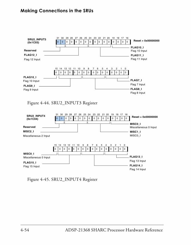
Making Connections in the SRUs
4-54 ADSP-21368 SHARC Processor Hardware Reference
Figure 4-44. SRU2_INPUT3 Register
Figure 4-45. SRU2_INPUT4 Register
31 30 29 28 27 26 25 24 23 22 21 20 19 18 17 16
00 0 0 0 0 0 0 0 0 0 0 0 0 0 0
Reserved
15 14 13 12 11 10 9 8 7 6 5 4 3 2 1 0
00 0 0 0 0 0 0 0 0 0 0 0 0 0 0
FLAG12_I
Flag 12 Input
FLAG10_IFlag 10 Input
FLAG11_IFlag 11 Input
FLAG9_IFlag 9 Input FLAG8_I
Flag 8 Input
FLAG7_I
Flag 7 Input
SRU2_INPUT3 (0x1C03)
FLAG10_IFlag 10 Input
Reset = 0x00000000
31 30 29 28 27 26 25 24 23 22 21 20 19 18 17 16
00 0 0 0 0 0 0 0 0 0 0 0 0 0 0
Reserved
15 14 13 12 11 10 9 8 7 6 5 4 3 2 1 0
00 0 0 0 0 0 0 0 0 0 0 0 0 0 0
MISC2_I
Miscellaneous 2 Input
MISC0_IMiscellaneous 0 Input
MISC1_IMISC0_I
FLAG15_IFlag 15 Input FLAG14_I
Flag 14 Input
FLAG13_I
Flag 13 Input
SRU2_INPUT4 (0x1C04)
MISC0_IMiscellaneous 0 Input
Reset = 0x00000000

ADSP-21368 SHARC Processor Hardware Reference 4-55
Digital Audio/Digital Peripheral Interfaces
Figure 4-46. SRU2_INPUT5 Register
Table 4-11. Group A Connections
Binary Decimal Signal Description
00000 00 LOGIC_LEVEL_LOW Logic level low (0)
00001 01 LOGIC_LEVEL_HIGH logic level high (1)
00010 02 DPI_P01_O External pin 1
00011 03 DPI_P02_O External pin 2
00100 04 DPI_P03_O External pin 3
00101 05 DPI_P04_O External pin 4
00110 06 DPI_P05_O External pin 5
00111 07 DPI_P06_O External pin 6
01000 08 DPI_P07_O External pin 7
01001 09 DPI_P08_O External pin 8
01010 10 DPI_P09_O External pin 9
01011 11 DPI_P10_O External pin 10
01100 12 DPI_P11_O External pin 11
31 30 29 28 27 26 25 24 23 22 21 20 19 18 17 16
00 0 0 0 0 0 0 0 0 0 0 0 0 0 0
Reserved
15 14 13 12 11 10 9 8 7 6 5 4 3 2 1 0
00 0 0 0 0 0 0 0 0 0 0 0 0 0 0
MISC8_I
Miscellaneous 8 Input
MISC6_IMiscellaneous 6 Input
MISC7_IMiscellaneous 7 Input
MISC5_IMiscellaneous 5 Input MISC4_I
Miscellaneous 4 Input
MISC3_I
Miscellaneous 3 Input
SRU2_INPUT5 (0x1C05)
MISC6_IMiscellaneous 6 Input
Reset = 0x00000000

Making Connections in the SRUs
4-56 ADSP-21368 SHARC Processor Hardware Reference
Group B Connections—Pin Assignment Signals
Group B connections, shown in Figure 4-47 through Figure 4-49 and Table 4-12, are used to route output signals to the 14 DPI pins.
01101 13 DPI_P12_O External pin 12
01110 14 DPI_P13_O External pin 13
01111 15 DPI_P14_O External pin 14
10000 16 TIMER0_O Timer0 output
10001 17 TIMER1_O Timer1 output
10010 18 TIMER2_O Timer2 output
10011 19 UART0_TX_O UART0 transmitter output
10100 20 UART1_TX_O UART1 transmitter output
10101-11111 21-31 RESERVED RESERVED
Figure 4-47. SRU2_PIN0 Register
Table 4-11. Group A Connections (Cont’d)
Binary Decimal Signal Description
31 30 29 28 27 26 25 24 23 22 21 20 19 18 17 16
10 0 1 1 0 0 0 0 0 0 0 0 0 0 0
Reserved
15 14 13 12 11 10 9 8 7 6 5 4 3 2 1 0
00 1 1 1 0 1 0 1 0 1 0 1 0 1 1
DPI_PB05_I
DPI pin buffer 5 Input
DPI_PB03_IDPI Pin Buffer 3 Input
DPI_PB04_IDPI Pin Buffer 4 Input
DPI_PB03_I
DPI_PB02_IDPI Pin Buffer2 Input
DPI_PB01_I
DPI Pin Buffer 1 Input
SRU2_PIN0 (0x01C10)
DPI Pin Buffer 3 Input
Reset = 0x30017556

ADSP-21368 SHARC Processor Hardware Reference 4-57
Digital Audio/Digital Peripheral Interfaces
Figure 4-48. SRU2_PIN1 Register
Figure 4-49. SRU2_PIN2 Register
Table 4-12. Group B Signals
Binary Decimal Signal Description
000000 00 LOGIC_LEVEL_LOW Logic level low (0)
000001 01 LOGIC_LEVEL_HIGH Logic level high (1)
000010 02 DPI_P01_O External pin 1
31 30 29 28 27 26 25 24 23 22 21 20 19 18 17 16
10 0 0 0 0 0 0 0 0 1 0 0 1 1 0
Reserved
15 14 13 12 11 10 9 8 7 6 5 4 3 2 1 0
11 0 1 1 0 1 1 0 1 0 0 1 1 0 0
DPI_PB10_I
DPI Pin Buffer 10 Input
DPI_PB08_IDPI Pin Buffer 8 Input
DPI_PB09_IDPI Pin Buffer 9 Input
DPI_PB08_I
DPI_PB07_IDPI Pin Buffer 7 Input
DPI_PB06_I
DPI Pin Buffer 6 Input
SRU2_PIN1 (0x01C11)
DPI Pin Buffer 8 Input
Reset = 0x002DB699
31 30 29 28 27 26 25 24 23 22 21 20 19 18 17 16
10 0 0 0 0 0 0 0 0 1 0 0 0 1 0
Reserved
15 14 13 12 11 10 9 8 7 6 5 4 3 2 1 0
00 0 0 0 0 0 0 0 0 0 0 0 0 0 0
DPI_PB13_IDPI Pin Buffer 13 Input
DPI_PB14_IDPI Pin Buffer 14 Input
DPI_PB13_I
DPI_PB12_IDPI Pin Buffer 12 Input
DPI_PB11_I
DPI Pin Buffer 11 Input
SRU2_PIN2 (0x01C12)
DPI Pin Buffer 13 Input
Reset = 0x00450000

Making Connections in the SRUs
4-58 ADSP-21368 SHARC Processor Hardware Reference
000011 03 DPI_P02_O External pin 2
000100 04 DPI_P03_O External pin 3
000101 05 DPI_P04_O External pin 4
000110 06 DPI_P05_O External pin 5
000111 07 DPI_P06_O External pin 6
001000 08 DPI_P07_O External pin 7
001001 09 DPI_P08_O External pin 8
001010 10 DPI_P09_O External pin 9
001011 11 DPI_P10_O External pin 10
001100 12 DPI_P11_O External pin 11
001101 13 DPI_P12_O External pin 12
001110 14 DPI_P13_O External pin 13
001111 15 DPI_P14_O External pin 14
010000 16 TIMER0_O Timer0 output
010001 17 TIMER1_O Timer1 output
010010 18 TIMER2_O Timer2 output
010011 19 UART0_TX_O UART0 transmitter output
010100 20 UART1_TX_O UART1 transmitter output
010101 21 SPI_MISO_O MISO from SPI
010110 22 SP_IM0SI_O MOSI from SPI
010111 23 SPI_CLK_O Clock output from SPI
011000 24 SPI_FLG0_O Slave select 0 from SPI
011001 25 SPI_FLG1_O Slave select 1 from SPI
011010 26 SPI_FLG2_O Slave select 2 from SPI
Table 4-12. Group B Signals (Cont’d)
Binary Decimal Signal Description

ADSP-21368 SHARC Processor Hardware Reference 4-59
Digital Audio/Digital Peripheral Interfaces
011011 27 SPI_FLG3_O Slave select 3 from SPI
011100 28 SPIB_MISO_O MISO from SPIB
011101 29 SPIB_M0SI_O MOSI from SPIB
011110 30 SPIB_CLK_O Clock output from SPIB
011111 31 SPIB_FLG0_O Slave select 0 from SPIB
100000 32 SPIB_FLG1_O Slave select 1 from SPIB
100001 33 SPIB_FLG2_O Slave select 2 from SPIB
100010 34 SPIB_FLG3_O Slave select 3 from SPIB
100011 35 FLAG4_O Flag 4 output
100100 36 FLAG5_O Flag 5 output
100101 37 FLAG6_O Flag 6 output
100110 38 FLAG7_O Flag 7 output
100111 39 FLAG8_O Flag 8 output
101000 40 FLAG9_O Flag 9 output
101001 41 FLAG10_O Flag 10 output
101010 42 FLAG11_O Flag 11 output
101011 43 FLAG12_O Flag 12 output
101100 44 FLAG13_O Flag 13 output
101101 45 FLAG14_O Flag 14 output
101110 46 FLAG15_O Flag 15 output
101111 47 PCG_CLKC_O Precision clock generator clock C out
110000 48 PCG_CLKD_O Precision clock generator clock D out
110001 49 PCG_FSC_O Precision clock generator frame sync C out
Table 4-12. Group B Signals (Cont’d)
Binary Decimal Signal Description

Making Connections in the SRUs
4-60 ADSP-21368 SHARC Processor Hardware Reference
Group C Connections—Pin Enable Signals
Group C signals, shown in Table 4-13 on page 4-62, are used to specify whether each DPI pin is used as an output or an input by setting the source for the pin buffer enable. When a pin buffer enable (DPI_PBENxx_I) is set (= 1), the signal present at the corresponding pin buffer input (DPI_PBxx_I) is driven off chip as an output. When a pin buffer enable is cleared (= 0), the signal present at the corresponding pin buffer input is ignored.
The registers that control group C settings are shown in Figure 4-50 through Figure 4-52.
The TWI output is an open-drain output so the pins used for TWI data and clock should be connected to logic level 0.
110010 50 PCG_FSD_O Precision clock generator frame sync D out
110011–111111
51-63 RESERVED
Table 4-12. Group B Signals (Cont’d)
Binary Decimal Signal Description

ADSP-21368 SHARC Processor Hardware Reference 4-61
Digital Audio/Digital Peripheral Interfaces
Figure 4-50. SRU2_PBEN0 Register
Figure 4-51. SRU2_PBEN1 Register
31 30 29 28 27 26 25 24 23 22 21 20 19 18 17 16
00 0 0 1 1 0 0 1 0 0 0 0 0 0 0
Reserved
15 14 13 12 11 10 9 8 7 6 5 4 3 2 1 0
11 1 0 0 0 0 1 0 1 0 0 0 1 0 1
DPI_PBEN05_I
DPI Pin Buffer Enable 5 Input
DPI_PBEN03_IDPI Pin Buffer Enable 3 Input
DPI_PBEN04_IDPI Pin Buffer Enable 4 Input
DPI_PBEN03_I
DPI_PBEN02_IDPI Pin Buffer Enable 2 Input
DPI_PBEN01_I
DPI Pin Buffer Enable 1 Input
SRU2_PBEN0 (0x01C20)
DPI Pin Buffer Enable 3 Input
Reset = 0x1900C28B
31 30 29 28 27 26 25 24 23 22 21 20 19 18 17 16
10 0 0 0 0 0 0 0 0 0 1 0 0 0 0
Reserved
15 14 13 12 11 10 9 8 7 6 5 4 3 2 1 0
00 0 0 0 0 0 1 1 1 1 0 0 1 1 1
DPI_PBEN10_I
DPI Pin Buffer Enable 10 Input
DPI_PBEN08_IDPI Pin Buffer Enable 8 Input
DPI_PBEN09_IDPI Pin Buffer Enable 9 Input
DPI_PBEN08_I
DPI_PBEN07_IDPI Pin Buffer Enable 7 Input
DPI_PBEN06_I
DPI Pin Buffer Enable 6 Input
SRU2_PBEN1 (0x01C21)
DPI Pin Buffer Enable 8 Input
Reset = 0x002103CE

Making Connections in the SRUs
4-62 ADSP-21368 SHARC Processor Hardware Reference
Figure 4-52. SRU2_PBEN2 Register
Table 4-13. Group C Signals
Binary Decimal Signal Description
000000 00 LOGIC_LEVEL_LOW Logic level low (0)
000001 01 LOGIC_LEVEL_HIGH Logic level high (1)
000010 02 EXT_MISC_0 Miscellaneous control 0
000011 03 EXT_MISC_1 Miscellaneous control 1
000100 04 EXT_MISC_2 Miscellaneous control 2
000101 05 TIMER0_PE_O Enable for timer 0 output
000110 06 TIMER1_PE_O Enable for timer 1 output
000111 07 TIMER2_PE_O Enable for timer 2 output
001000 08 UART0_TX_PE_0 Pin enable for UART 0 transmitter
001001 09 UART1_TX_PE_0 Pin enable for UART 1 transmitter
001010 10 SPIMISO_PE_O Pin enable for MISO from SPI
001011 11 SPIMOSI_PE_O Pin enable for MOSI froM SPI
001100 12 SPICLK_PE_O Pin enable for CLK from SPI
31 30 29 28 27 26 25 24 23 22 21 20 19 18 17 16
00 0 0 0 0 0 0 0 0 0 0 1 1 0 0
Reserved
15 14 13 12 11 10 9 8 7 6 5 4 3 2 1 0
00 1 0 1 1 0 0 1 0 1 1 0 0 1 0
DPI_PBEN13_IDPI Pin Buffer Enable 13 Input
DPI_PBEN14_IDPI Pin Buffer Enable 14 Input
DPI_PBEN13_I
DPI_PBEN12_IDPI Pin Buffer Enable 12 Input
DPI_PBEN11_I
DPI Pin Buffer Enable 11 Input
SRU2_PBEN2 (0x01C22)
DPI Pin Buffer Enable 13 Input
Reset = 0x00185964

ADSP-21368 SHARC Processor Hardware Reference 4-63
Digital Audio/Digital Peripheral Interfaces
001101 13 SPIFLG0_PE_O Pin enable for slave select 0 from SPI
001110 14 SPIFLG1_PE_O Pin enable for slave select 1 from SPI
001111 15 SPIFLG2_PE_O Pin enable for slave select 2 from SPI
010000 16 SPIFLG3_PE_O Pin enable for slave select 3 from SPI
010001 17 SPIBMISO_PE_O Pin enable for MISO from SPIB
010010 18 SPIBMOSI_PE_O Pin enable for MOSI from SPIB
010011 19 SPIBCLK_PE_O Pin enable for CLK from SPIB
010100 20 SPIBFLG0_PE_O Pin enable for slave select 0 from SPIB
010101 21 SPIBFLG1_PE_O Pin enable for slave select 1 from SPIB
010110 22 SPIBFLG2_PE_O Pin enable for slave select 2 from SPIB
010111 23 SPIBFLG3_PE_O Pin enable for slave select 3 from SPIB
011000 24 FLAG4_PE_O Pin enable for Flag 4 output
011001 25 FLAG5_PE_O Pin enable for Flag 5 output
011010 26 FLAG6_PE_O Pin enable for Flag 6 output
011011 27 FLAG7_PE_O Pin enable for Flag 7 output
011100 28 FLAG8_PE_O Pin enable for Flag 8 output
011101 29 FLAG9_PE_O Pin enable for Flag 9 output
011110 30 FLAG10_PE_O Pin enable for Flag 10 output
011111 31 FLAG11_PE_O Pin enable for Flag 11 output
100000 32 FLAG12_PE_O Pin enable for Flag 12 output
100001 33 FLAG13_PE_O Pin enable for Flag 13 output
100010 34 FLAG14_PE_O Pin enable for Flag 14 output
100011 35 FLAG15_PE_O Pin enable for Flag 15 output
100100 36 TWI_SDATA_OE Serial data output enable from TWI
Table 4-13. Group C Signals (Cont’d)
Binary Decimal Signal Description

General-Purpose I/O (GPIO) and Flags
4-64 ADSP-21368 SHARC Processor Hardware Reference
The pin enable control registers activate the drive buffer for each of the 14 DPI pins. When the pins are not enabled (driven), they can be used as inputs.
General-Purpose I/O (GPIO) and Flags Each interface is capable of using its pins for general-purpose I/O and flags. The sections that follow describe this use for each interface.
DAI GPIO and FlagsIn the DAI, any of the pins may also be considered general-purpose input/output (GPIO) pins. Each of the DAI pins can also be set to drive a high or low logic level signal to assert signals. They can also be connected to miscellaneous signals and used as interrupt sources or as control inputs to other blocks.
100101 37 TWI_SCLK_OE Serial clock output enable from TWI
100110 38 EXT_MISC_3 Miscellaneous control 3
100111 39 EXT_MISC_4 Miscellaneous control 4
101000 40 EXT_MISC_5 Miscellaneous control 5
101001 41 EXT_MISC_6 Miscellaneous control 6
101010 42 EXT_MISC_7 Miscellaneous control 7
101011 43 EXT_MISC_8 Miscellaneous control 8
101100–111111
44-63 Reserved
Table 4-13. Group C Signals (Cont’d)
Binary Decimal Signal Description

ADSP-21368 SHARC Processor Hardware Reference 4-65
Digital Audio/Digital Peripheral Interfaces
DPI GPIO and FlagsIn the DPI, the EXT_MISC signals are used for general-purpose I/O. An interrupt controller processes these signals to generate an interrupt, for example DPI_INT. The EXT_MISC signals can also be used to control pin enables. Flags 4-15 can be routed using the DPI pins.
Miscellaneous SignalsIn the ADSP-21367/8/9 and ADSP-2137x processors, exception applica-tions can also configure signals to:
• Act as interrupt sources
• Act as inverted signals (forcing a signal to active low)
• Connect one pin to another
• Act as pin enables
DAI/DPI Interrupt ControllerThe DAI contains a dedicated interrupt controller that signals the core when DAI peripheral events occur.
Relationship to the CoreGenerally, interrupts are classified as catastrophic or normal. Catastrophic events include any hardware interrupts (for example, resets) and emula-tion interrupts (under the control of the PC), math exceptions, and “reads” of memory that do not exist. Catastrophic events are treated as high priority events. In comparison, normal interrupts are “determinis-tic”—specific events emanating from a source (the causes), the result of which is the generation of an interrupt. The expiration of a timer can

DAI/DPI Interrupt Controller
4-66 ADSP-21368 SHARC Processor Hardware Reference
generate an interrupt, a signal that a serial port has received data that must be processed, a signal that an SPI has either transmitted or received data, and other software interrupts like the insertion of a trap that causes a breakpoint—all are conditions, which identify to the core that an event has occurred.
Since DAI specific events generally occur infrequently, the DAI IC classi-fies such interrupts as either high or low priority interrupts. Within these broad categories, programs can indicate which interrupts are high and which are classified as low.
Any interrupt causes a four-cycle stall, since it forces the core to stop instruction execution while in process, then vector to the interrupt service routine (ISR), (which is basically an interrupt vector table (IVT) lookup), then proceed to implement the instruction referenced in the IVT. For more information, see Appendix B, Interrupts.
When an interrupt from the DAI needs servicing, one of the two core interrupt service routines (ISR) must query the DAI’s interrupt controller to determine the source(s). Sources can be any one or more of the inter-rupt controller’s 32 configurable channels (DAI_INT[31:0]). For more information, see “DAI Interrupt Controller Registers” on page A-112.
DAI events trigger two interrupts in the primary IVT—one each for low or high priority.
DAI InterruptsThere are several registers in the DAI interrupt controller that can be con-figured to control how the DAI interrupts are reported to and serviced by the core’s interrupt controller. Among other options, each DAI interrupt can be mapped either as a high or low priority interrupt in the primary interrupt controller. Certain DAI interrupts can be triggered on either the rising or the falling edge of the signals, and each DAI interrupt can also be independently masked.

ADSP-21368 SHARC Processor Hardware Reference 4-67
Digital Audio/Digital Peripheral Interfaces
Just as the core has its own interrupt latch registers (IRPTL and LIRPTL), the DAI has its own latch registers (DAI_IRPTL_L and DAI_IRPTL_H). When a DAI interrupt is configured to be high priority, it is latched in the DAI_IRPTL_H register. When any bit in the DAI_IRPTL_H register is set (= 1), bit 11 in the IRPTL register is also set and the core services that interrupt with high priority. When a DAI interrupt is configured to be low priority, it is latched in the DAI_IRPTL_L register. Similarly, when any bit in the DAI_IRPTL_L register is set (= 1), bit 6 in the LIRPTL register is also set and the core services that interrupt with low priority. Regardless of the priority, when a DAI interrupt is latched and promoted to the core interrupt latch, the ISR must query the DAI’s interrupt controller to determine the source(s). Sources can be any one or more of the interrupt controller’s 32 configurable channels (DAI_INT31–0). For more informa-tion, see “DAI Interrupt Controller Registers” on page A-112.
Reading the DAI’s interrupt latches clears them. Therefore, the ISR must service all the interrupt sources it discovers. That is, if multiple interrupts are latched in one of the DAI_IRPTL_x registers, all of them must be serviced before executing an RTI instruction.
The IDP_FIFO_GTN_INT interrupt is not cleared when the DAI_IRPTL_H/L registers are read. This interrupt is cleared automatically when the situa-tion that caused the interrupt goes away.
DPI InterruptsThe DPI also has an interrupt controller, similar to that in the DAI. There are 14 interrupts—4 from the UARTs, 1 from the two wire interface (TWI) and 9 general-purpose I/O interrupts. All of these interrupts are combined into a single interrupt, namely DPI_INT. The DPI_IRPTL register contains the status on individual interrupts. Apart from DPI_IRPTL, there are two additional registers, DPI_IRPTL_RE and DPI_IRPTL_FE which are used for interrupt latching. Setting a corresponding bit in the DPI_IRPTL_RE register enables interrupt latching at the rising edge of the corresponding signal. Similarly, setting a corresponding bit in the

DAI/DPI Interrupt Controller
4-68 ADSP-21368 SHARC Processor Hardware Reference
DPI_IRPTL_FE register enables interrupt latching at the falling edge of that signal. A particular interrupt can be latched at the rising or falling edge independently. Keeping corresponding bits reset in both these registers (DPI_IRPTL_RE and DPI_IRPTL_FE) disables the corresponding interrupt.
The DPI_INT interrupt is automatically cleared when the DPI_IRPTL register is read for the EXT_MISC, UART_TX, and UART_RX (for DMA mode only) interrupts. Furthermore, the UART_RX interrupt for I/O mode must be cleared in the ISR. For information on using inter-rupts in the UART, see “UARTxIER Register” on page 11-7, and “UARTxIIR Register” on page 11-9. For information on using interrupts in the TWI, see “Interrupt Source Register” on page 12-7 and “Interrupt Enable Register” on page 12-8.
The UART and TWI interrupts are only used as rising edge interrupts. The corresponding bits in the DPI_IRPTL_FE register are reserved. By default, at reset, all interrupts are disabled (in other words, both the DPI_IRPTL_RE and DPI_IRPTL_FE registers have zero values).
Interrupt service routines (ISR) must read the DPI_IRPTL register to dis-cover all of the interrupts that are currently latched. A shadow register, DPI_IRPTL_SH, is provided for the primary register DPI_IRPTL. Reads of this register returns data in the DPI_IRPTL register without clearing the contents of the register.
Note that the ISR must make sure that the current interrupt condition is removed before exiting to the main program. Further note that for the interrupts corresponding to the UART and the TWI, the bits in the DPI_IRPTL_RE register are used as enable bits and corresponding bits from the DPI_IRPTL_FE register are not used.

ADSP-21368 SHARC Processor Hardware Reference 4-69
Digital Audio/Digital Peripheral Interfaces
High and Low Priority Latches In the ADSP-21367/8/9 and ADSP-2137x processors, a pair of registers (DAI_IRPTL_H and DAI_IRPTL_L) replace functions normally performed by the IRPTL register. A single register (DAI_IRPTL_PRI) specifies the latch to which each of these interrupts are mapped.
Two registers (DAI_IRPTL_RE and DAI_IRPTL_FE) replace the DAI periph-eral’s version of the IMASK register. As with the IMASK register, these DAI registers provide a way to specify which interrupts to notice and handle, and which interrupts to ignore. These dual registers function like IMASK does, but with a higher degree of granularity.
Signals from the SRU can be used to generate interrupts. For example, when SRU_EXTMISCA2_INT (bit 30) of DAI_IRPTL_H is set to one, any signals from the external miscellaneous channel 2 generate an interrupt. If set to one, DAI interrupts trigger an interrupt in the core and the interrupt latch is set. A read of this bit does not reset it to zero. The bit is only set to zero when the cause of the interrupt is cleared. A DAI interrupt indicates the source (in this case, external miscellaneous A, channel 2), and checks the IVT for an instruction (next operation) to perform.
The 32 interrupt signals within the interrupt controller are mapped to 2 interrupt signals in the primary interrupt controller of the SHARC pro-cessor core. The DAI_IRPTL_PRI register specifies if the interrupt controller interrupt is mapped to the high or low core interrupt (1 = high priority and 0 = low priority).
The DAI_IRPTL_H register is a read-only register with bits set for every DAI interrupt latched for the high priority core interrupts. The DAI_IRPTL_L register is a read-only register with bits set for every DAI interrupt latched for the low priority core interrupts. When a DAI interrupt occurs, the low or high priority core ISR interrogates its corresponding register to deter-mine which of the 32 interrupt sources to service. When the DAI_IRPTL_H

DAI/DPI Interrupt Controller
4-70 ADSP-21368 SHARC Processor Hardware Reference
register is read, the high priority latched interrupts are all cleared. When the DAI_IRPTL_L register is read, the low priority latched interrupts are all cleared.
Rising and Falling Edge MasksFor interrupt sources that correspond to waveforms (as opposed to DAI event signals such as DMA complete or buffer full), the edge of a wave-form may be used as an interrupt source as well. Just as interrupts can be generated by a source, interrupts can also be generated and latched on the rising (or falling) edges of a signal. This concept does not exist in the main interrupt controller—only in the DAI interrupt controller.
When a signal comes in, the system needs to determine what kind of sig-nal it is and what kind of protocol, as a result, to service. The preamble indicates the signal type. When the protocol changes, output (signal) type is noted.
For audio applications, the ADSP-21367/8/9 and ADSP-2137x processors need information about interrupt sources that correspond to waveforms (not event signals). As a result, the falling edge of the waveform may be used as an interrupt source as well. Programs may select any of these four conditions:
• Latch on the rising edge
• Latch on the falling edge
• Latch on both the rising and falling edge
The DAI interrupt controller may be configured using three registers. Each of the 32 interrupt lines can be independently configured to trigger in response to the incoming signal’s rising edge, its falling edge, or both the rising edge and the falling edge. Setting a bit in either the

ADSP-21368 SHARC Processor Hardware Reference 4-71
Digital Audio/Digital Peripheral Interfaces
DAI_IRPTL_RE or DAI_IRPTL_FE registers enables the interrupt level on the rising and falling edges, respectively. For more information on these regis-ters, see “DAI Interrupt Controller Registers” on page A-112.
Programs can manage responses to signals by configuring registers. In a sample audio application, for example, upon detection of a change of pro-tocol, the output can be muted. This change of output and the resulting behavior (causing the sound to be muted) results in an alert signal (an interrupt) being introduced in response (if the detection of a protocol change is a high priority interrupt).
The DAI_IRPTL_FE register can only be used for latching interrupts on the falling edge.
Use of the DAI_IRPTL_RE or DAI_IRPTL_FE registers allows programs to notice and respond to rising edges, falling edges, both rising and falling edges, or neither rising nor falling edges so they can be masked separately.
Responses to changes in conditions of signals (including changes in DMA state, introduction of error conditions, and so on) can only be enabled using the DAI_IRPTL_RE register.
Configuring Peripherals Using SRU1The following sections describe how the various peripherals associated with SRU1 are configured.
Configuring the SPORTsThe serial port chapter provides the signal sensitivity information of the SPORT signals which needs to be considered while configuring the serial ports using DAI pins. For more information, see “Serial Port Signal Sensi-tivity” on page 5-9.

Configuring Peripherals Using SRU2
4-72 ADSP-21368 SHARC Processor Hardware Reference
Configuring the PCGs“Precision Clock Generators” on page 13-1 provides extensive informa-tion on programming using the DAI. “Clock and Frame Sync Divisors PCG Channel B” on page 13-20 is an example program that uses PCG channel B to output a clock on DAI pin 1 and a frame sync on DAI pin 2.
Configuring Peripherals Using SRU2The following sections describe how the various peripherals associated with SRU2 are configured.
Configuring the SPIAll SPI signals are routed through the SRU2 and are routed as described in “Signal Routing Units” on page 4-8, Figure 4-3 on page 4-6 and Figure 4-4 on page 4-7. Normally, it is acceptable to enable (SRU2) out-put buffers to permanently ground the pin enable signals. However, this does not work for the open-drain mode, because the SRU2 buffer always actively drives the output pin. Where open-drain mode is used, the pin enable signals must be connected to the pin enable associated with the SPI SRU2 buffers and connected with the SPIB_MISO_O, SPIB_MOSI_O, SPIB_CLK_O, and SPIB_FLGx_O pins. For more information on open-drain mode, see “Open Drain Mode (OPD)” on page 6-9.
Choosing the Pin Enable for the SPI Clock
When in SPI master mode, the SPICLK signal is sent from the processor. The enable signal for the DPI pin being used for the clock must be con-nected correctly depending on the SPI mode being used (based on the setting of CPHASE and CLKPL bits in the SPICTL register). Table 4-14 shows the correct pin enable to use by SPI mode.

ADSP-21368 SHARC Processor Hardware Reference 4-73
Digital Audio/Digital Peripheral Interfaces
As an example, the output of the clock to DPI pin 3 would be configured in SPI mode 3 as follows.
SRU(SPI_CLK_O,DPI_PB03_I);
SRU(SPI_CLK_O,DPI_PBEN03_I);
Configuring the Two Wire InterfaceEach TWI device, whether master or slave, responds to the other devices with an acknowledge bit when data is received. For details, see Chapter 12, Two Wire Interface Controller. For proper operation, the SRU must be set up so that data communication is possible in both direc-tions on the data pin.
The examples in Listing 4-1 through Listing 4-4 show the SRU settings for different TWI modes.
Listing 4-1. TWI Master Transmit Mode
SRU(LOW,DPI_PB11_I) /* Since TWI output is an open-drain
output, the TWI pin is connected
to logic level low */
SRU(TWI_DATA_PBEN_O,DPI_PBEN11_I) /* TWI data output connected
to DPI pin 11 input */
Table 4-14. SPI Pin Enable Selections
Mode CLKPL CPHASE Use Pin Enable...
0 0 0 HIGH
1 0 1 HIGH
2 1 0 SPI_CLK_O
3 1 1 SPI_CLK_O

Configuring Peripherals Using SRU2
4-74 ADSP-21368 SHARC Processor Hardware Reference
SRU(DPI_PB11_O, TWI_DATA_I); /* DPI pin 11 output connected
to TWI data input */
SRU(LOW,DPI_PB12_I) /* Since TWI output is an open-drain
output, the TWI pin is connected
to logic level low */
SRU2(TWI_CLK_PBEN_O,DPI_PBEN12_I) /* TWI clock connected to DPI
pin 12 */
Listing 4-2. TWI Master Receive Mode
SRU(DPI_PB11_O,TWI_DATA_I) /* DPI pin 11 output connected to
TWI data input */
SRU(LOW,DPI_PB11_I) /* Since TWI output is an open-drain
output the TWI pin is connected to
logic level low */
SRU(TWI_DATA_PBEN_O,DPI_PBEN11_I) ) /* TWI data output
connected to DPI pin 11
input */
SRU(LOW,DPI_PB12_I) ) /* Since TWI output is an open-drain
output the TWI pin is connected to
logic level low */
SRU(TWI_CLK_PBEN_O,DPI_PBEN12_I) /* TWI Clock connected to DPI
pin 12

ADSP-21368 SHARC Processor Hardware Reference 4-75
Digital Audio/Digital Peripheral Interfaces
Listing 4-3. TWI Slave Transmit Mode
SRU(LOW,DPI_PB11_I) /* Since TWI output is an open-drain
output the TWI pin is connected
to logic level low */
SRU(TWI_DATA_PBEN_O,DPI_PBEN11_I) /* TWI data output connected
to DPI pin 11 input */
SRU(DPI_PB11_O,TWI_DATA_I) /* DPI pin 11 output connected to
TWI data input */
SRU(DPI_PB12_O, TWI_CLK_I) /* clock signal from DPI pin 12 is
connected to the TWI slave
clock input */
SRU(LOW,DPI_PBEN12_I) /* Disables DPI pin 12 as input as
the clock is not generated by
the slave */
Listing 4-4. TWI Slave Receive Mode
SRU(DPI_PB11_O,TWI_DATA_I /* DPI pin 11 output connected to
TWI data input */
SRU(LOW,DPI_PB11_I) ) /* Since TWI output is an open
drain output the TWI pin is
connected to logic level low */
SRU2(TWI_DATA_PBEN_O,DPI_PBEN11_I) /* TWI data output
connected to DPI pin
11 input */

Using the SRU() Macro to Configure the DAI
4-76 ADSP-21368 SHARC Processor Hardware Reference
SRU2(DPI_PB12_O, TWI_CLK_I) /* Clock signal from DPI pin 12
is connected to the TWI slave
clock input */
SRU2(LOW,DPI_PBEN12_I) ) /* Disables DPI pin 12 as input as
the clock is not generated by
the slave */
Using the SRU() Macro to Configure the DAI
As discussed in the previous sections, the signal routing unit (SRU) is con-trolled by writing values that correspond to signal sources into bit fields that further correspond to signal inputs. The SRU is arranged into func-tional groups such that registers that are made up of these bit fields accept a common set of source signal values.
In order to ease the coding process, the header file sru.h is included with the VisualDSP++ tools. This file implements a macro that automates most of the work of signal assignments and functions. The macro has identical syntax in C/C++ and assembly, and makes a single connection from an output to an input:
SRU(Output Signal, Input Signal);
The names passed to the macro are the names given in Table 4-4 through Table 4-9 and in the DAI registers section in “DAI/SRU1 Connection Groups” on page 4-18. To use this macro, add the code shown in Listing 4-5 to your source code.

ADSP-21368 SHARC Processor Hardware Reference 4-77
Digital Audio/Digital Peripheral Interfaces
Listing 4-5. DAI Macro Code
#include <sru.h>;
/* The following lines illustrate how the macro is used: */
/* Route SPORT 1 clock output to pin buffer 5 input */
SRU(SPORT1_CLK_O,DAI_PB05_I);
/* Route pin buffer 14 out to IDP3 frame sync input */
SRU(DAI_PB14_O,IDP3_FS_I);
/* Connect pin buffer enable 19 to logic low */
SRU(LOW,DAI_PBEN19_I);
Additional example code is available on the Analog Devices Web site.
There is a macro that has been created to connect peripherals used in a DAI configuration. This code can be used in both assembly and C code. See the INCLUDE file SRU.H.
There is also a software plug-in called the Expert DAI that greatly simplifies the task of connecting the signals described in this chap-ter. This plug-in is described in Engineer-to-Engineer Note EE-243, “Using the Expert DAI for ADSP-2126x and ADSP-2136x SHARC Processors”. This EE note is also found on the Analog Devices Web site.

Using the SRU() Macro to Configure the DAI
4-78 ADSP-21368 SHARC Processor Hardware Reference

ADSP-21368 SHARC Processor Hardware Reference 5-1
5 SERIAL PORTS
The ADSP-21367/8/9 and ADSP-2137x processors have up to eight inde-pendent, synchronous serial ports (SPORTs) that provide an I/O interface to a wide variety of peripheral devices. They are called SPORT0, SPORT1, SPORT2, SPORT3, SPORT4, SPORT 5, SPORT6, and SPORT7. Each SPORT has its own set of control registers and data buff-ers. With a range of clock and frame synchronization options, the SPORTs allow a variety of serial communication protocols and provide a glueless hardware interface to many industry-standard data converters and CODECs.
Serial ports can operate at one-eighth the full clock rate of the processor, a maximum rate of 50M bit/s for (CCLK) = 3 ns. If channels A and B are active, each SPORT has 83.3M bit/s maximum total throughput. Bidirec-tional (transmit or receive) functions provide greater flexibility for serial communications. Serial port data can be automatically transferred to and from on-chip memory using DMA block transfers. In addition to standard synchronous serial mode, each SPORT offers a time division multiplexed (TDM) multichannel mode, left-justified sample pair mode, and I2S mode.
Features
5-2 ADSP-21368 SHARC Processor Hardware Reference
FeaturesSerial ports offer the following additional features and capabilities:
• Two additional SPORTs, each with their own DMA channels and interrupts, have been added to the ADSP-21367, ADSP-21368, ADSP-21369, and ADSP-21371 SHARC processors.
• Two bidirectional channels (A and B) per SPORT, configurable as either transmitters or receivers. Each SPORT can also be config-ured as two receivers or two transmitters, permitting two unidirectional streams into or out of the same SPORT. This bidi-rectional functionality provides greater flexibility for serial communications. Further, two SPORTs can be combined to enable full-duplex, dual-stream communications.
• All serial data signals have programmable receive and transmit functions and thus have one transmit and one receive data buffer register (double buffer). There is also a bidirectional shift register associated with each serial data signal. Double buffering provides additional time to service the SPORT.
• A serial clock and frame sync provide signals in a wide range of fre-quencies. Alternately, the SPORT can accept clock and frame sync input from an external source, as described in Figure 5-10 on page 5-70.
• The processors allow interrupt-driven, single word transfers to and from on-chip memory controlled by the core, described in “Single Word Transfers” on page 5-81.
• DMA transfers to and from on-chip memory. Each SPORT can automatically receive or transmit an entire block of data. Further the SPORTs on the processors offer chained DMA operations for multiple data blocks, see “Chaining DMA Processes” on page 2-14.

ADSP-21368 SHARC Processor Hardware Reference 5-3
Serial Ports
New DMA channels are added for SPORT6 and 7. These new SPORTs also have their own interrupt lines.
Operation ModesThee serial ports have four operation modes: standard DSP serial, left-jus-tified sample pair, I2S, and multichannel. In standard DSP serial, left-justified sample pair and I2S modes, when both A and B channels are used, they transmit or receive data simultaneously, sending or receiving bit 0 on the same edge of the serial clock, bit 1 on the next edge of the serial clock, and so on. In multichannel mode, SPORTs can receive and trans-mit A and B channel data selectively from up to 128 channels of a TDM serial bit stream. See “SPORT Operation Modes” on page 5-10.
For the ADSP-21367/8/9 and ADSP-2137x processors in multi-channel mode, there are several enhancements from previous SHARC processors.
• In previous SHARC processors, SPORTs were forced into pairs when in multichannel mode. The SPORTs in the ADSP-21367/8/9 and ADSP-2137x processors now operate independently.
• In addition, control registers are added to each SPORT. In previ-ous versions, there was only one TDM control register for each SPORT pair.
• New data valid pins are added to each SPORT. In previous ver-sions, in paired mode, the frame sync of one of the SPORTs was used as a data valid pin so eight new pin definitions are added to the SRU.

Operation Modes
5-4 ADSP-21368 SHARC Processor Hardware Reference
• In multichannel mode, support for packed I2S mode is new for the ADSP-21367/8/9 and ADSP-2137x processors. However, it should be noted that packed I2S mode is not identical to I2S mode in all cases. For more information, see “Packed I2S Mode” on page 5-33.
• Even though SPORTs can operated independently in TDM mode, compression and expansion logic is only available in SPORT0, 2, 4, and 6 and expansion logic is available only in SPORT1, 3, 5 and 7.
• The Frame sync error detection logic is added for the ADSP-21367/8/9 and ADSP-2137x processors. It detects frame syncs coming early where the frame sync arrives while transmis-sion/reception of previous word is occurring. It does not detect errors such as frame syncs arriving late. One dedicated error inter-rupt is added which is shared by all sports.
The SPORTs are configurable for transferring data words between 3 and 32 bits in length, either most significant bit (MSB) first or least significant bit (LSB) first. Words must be between 8 and 32 bits in length for I2S and left-justified sample pair mode. Refer to “Data Word Formats” on page 5-43 and the individual SPORTs operation mode sections for addi-tional information.
Multichannel mode operation supports 128-channel TDM, described in “Multichannel Operation” on page 5-25.
Receive comparison and two-dimensional DMA are not supported in the ADSP-21367/8/9 and ADSP-2137x.
The SPTRAN bit in the SPCTLx register affects the operation of the transmit or the receive data paths. The data path includes the data buffers and the shift registers. When SPTRAN = 0, the primary and secondary RXSPxy data buffers and receive shift registers are activated, and the transmit path is disabled. When SPTRAN = 1, the primary and secondary TXSPxy data buff-ers and transmit shift registers are activated, and the receive path is disabled.

ADSP-21368 SHARC Processor Hardware Reference 5-5
Serial Ports
Serial Port SignalsFigure 5-1 shows the SPORT signals (note that not all models have eight SPORTs). Any 20 of these 32 signals can be mapped to digital audio interface (DAI_Px) pins through the signal routing unit (SRU1). For more information, see Chapter 4, Digital Audio/Digital Peripheral Interfaces.
Figure 5-1. DSP Standard Serial Mode – Serial Port Signals
S P O R T 4
S P O R T 5
S P O R T4 _D A
S P O R T4 _D B
S P O R T 4_ C L K
S P O R T4 _F S
S P O R T5 _D A
S P O R T5 _D B
S P O R T 5_ C L K
S P O R T5 _F S
S P O R T 4 _ D A = S P O R T4 C H A N N E L A D A T A (R X O R T X )S P O R T 4 _ D B = S P O R T4 C H A N N E L B D A T A (R X O R T X )S P O R T 4 _ C L K = S P O R T4 S E R IA L C L O C KS P O R T 4 _ FS = S P O R T4 F R A M E S Y N CS P O R T 4 _ TD V = S P O R T4 T R A N S M IT D A TA V A L IDS P O R T 5 _ D A = S P O R T5 C H A N N E L A D A T A (R X O R T X )S P O R T 5 _ D B = S P O R T5 C H A N N E L B D A T A (R X O R T X )S P O R T 5 _ C L K = S P O R T5 S E R IA L C L O C KS P O R T 5 _ FS = S P O R T5 F R A M E S Y N CS P O R T 5 _ TD V = S P O R T5 T R A N S M IT D A TA V A L ID
S P O R T 0
S P O RT 0 _D A
S P O RT 0 _D B
S P O R T 0_ C LK
S P O RT 0 _F S
S P O R T 1
S P O R T 1_ D A
S P O R T 1_ D B
S P O R T 1_C L K
S P O R T 1_ F S
S P O R T 0_ D A _ IO
S P O R T 0_ D B _ IO
S P O R T 0_ C L K _ IO
S P O R T 0 _F S _ IO
S P O R T 1_ DA _ IO
S P O R T 1_ DB _ IO
S P O R T1 _C L K _ IO
S P O R T 1_ F S _ IO
S P O R T 2_ D A _ IO
S P O R T 2_ D B _ IO
S P O R T 2_ C LK _ IO
S P O RT 2 _F S _ IO
S P O R T 3_ D A _ IO
S P O R T 3_ D B _ IO
S P O R T 3_ C LK _ IO
S P O RT 3 _F S _ IO
S P O R T 4_ D A _ IO
S P O R T 4_ D B _ IO
S P O R T 4_ C LK _ IO
S P O RT 4 _F S _ IO
S P O R T 5_ D A _ IO
S P O R T 5_ D B _ IO
S P O R T 5_ C LK _ IO
S P O RT 5 _F S _ IO
S IG N A L R O U T I N GU N IT ( S R U )
S P O R T 2
S P O R T 3
S P O R T2 _D A
S P O R T2 _D B
S P O R T 2 _C L K
S P O R T2 _F S
S P O R T3 _D A
S P O R T3 _D B
S P O R T 3 _C L K
S P O R T3 _F S
S E R IA L P O R T S P O R T S I G N A L S
S P O R T 2 _ D A = S P O R T2 C H A N N E L A D A T A ( R X O R T X )S P O R T 2 _ D B = S P O R T2 C H A N N E L B D A T A ( R X O R T X )S P O R T 2 _ C L K = S P O R T2 S E R IA L C LO C KS P O R T 2 _ FS = S P O R T2 F R A M E S Y N CS P O R T 2 _ TD V = S P O R T2 T R A N S M IT D A T A V A L IDS P O R T 3 _ D A = S P O R T3 C H A N N E L A D A T A ( R X O R T X )S P O R T 3 _ D B = S P O R T3 C H A N N E L B D A T A ( R X O R T X )S P O R T 3 _ C L K = S P O R T3 S E R IA L C LO C KS P O R T 3 _ FS = S P O R T3 F R A M E S Y N CS P O R T 3 _ TD V = S P O R T3 T R A N S M IT D A T A V A L ID
S P O R T 0 _ D A = S P O R T0 C H A N N E L A D A T A (R X O R T X )S P O R T 0 _ D B = S P O R T0 C H A N N E L B D A T A (R X O R T X )S P O R T 0 _ C L K = S P O R T0 S E R IA L C L O C KS P O R T 0 _ FS = S P O R T0 F R A M E S Y N CS P O R T 0 _ TD V = S P O R T0 T R A N S M IT D A TA V A L IDS P O R T 1 _ D A = S P O R T1 C H A N N E L A D A T A (R X O R T X )S P O R T 1 _ D B = S P O R T1 C H A N N E L B D A T A (R X O R T X )S P O R T 1 _ C L K = S P O R T1 S E R IA L C L O C KS P O R T 1 _ FS = S P O R T1 F R A M E S Y N CS P O R T 1 _ TD V = S P O R T1 T R A N S M IT D A TA V A L ID
S P O R T 6
S P O R T 7
S P O R T6 _D A
S P O R T6 _D B
S P O R T 6_ C L K
S P O R T6 _F S
S P O R T7 _D A
S P O R T7 _D B
S P O R T 7_ C L K
S P O R T7 _F S
S P O R T 6 _ D A = S P O R T6 C H A N N E L A D A T A (R X O R T X )S P O R T 6 _ D B = S P O R T6 C H A N N E L B D A T A (R X O R T X )S P O R T 6 _ C L K = S P O R T6 S E R IA L C L O C KS P O R T 6 _ FS = S P O R T6 F R A M E S Y N CS P O R T 6 _ TD V = S P O R T6 T R A N S M IT D A TA V A L IDS P O R T 7 _ D A = S P O R T7 C H A N N E L A D A T A (R X O R T X )S P O R T 7 _ D B = S P O R T7 C H A N N E L B D A T A (R X O R T X )S P O R T 7 _ C L K = S P O R T7 S E R IA L C L O C KS P O R T 7 _ FS = S P O R T7 F R A M E S Y N CS P O R T 7 _ TD V = S P O R T7 T R A N S M IT D A TA V A L ID
S P O R T 6_ DA _ IO
S P O R T 6_ DB _ IO
S P O R T6 _C L K _ IO
S P O R T 6_ F S _ IO
S P O R T 7_ DA _ IO
S P O R T 7_ DB _ IO
S P O R T7 _C L K _ IO
S P O R T 7_ F S _ IO
S P O RT 0_T D VS P O R T 0_ T D V _P B E N _O
S P O R T 1_ TD VS P O R T1 _T D V _ P B E N _O
S P O R T 2_ T D VS P O R T 2 _T D V _P B E N _O
S P O R T 3_ T D VS P O R T3 _T D V _ P B E N _O
S P O R T 4_ T D VS P O R T 4_ T D V _P B E N _ O
S P O R T 5_ T D VS P O R T 5_ T D V _P B E N _ O
S P O R T 6_ T D VS P O R T 6 _T D V _ P B E N _O
S P O R T 7_ T D VS P O R T7 _T D V _ P B E N _ O

Serial Port Signals
5-6 ADSP-21368 SHARC Processor Hardware Reference
Pairings of SPORTs (0 and 1, 2 and 3, and 4 and 5, 6 and 7) are used only in loopback mode for testing.
A SPORT receives serial data on one of its bidirectional serial data signals configured as inputs, or transmits serial data on the bidirectional serial data signals configured as outputs. It can receive or transmit on both channels simultaneously and unidirectionally, where the pair of data sig-nals can both be configured as either transmitters or receivers.
The SPORTx_DA and SPORTx_DB channel data signals on each SPORT can-not transmit and receive data simultaneously for full-duplex operation. Two SPORTs must be combined to achieve full-duplex operation. The SPTRAN bit in the SPCTLx register controls the direction for both the A and B channel signals. Therefore, the direction of channel A and channel B on a particular SPORT must be the same.
Serial communications are synchronized to a clock signal. Every data bit must be accompanied by a clock pulse. Each SPORT can generate or receive its own clock signal (SPORTx_CLK). Internally-generated serial clock frequencies are configured in the DIVx registers. The A and B channel data signals shift data based on the rate of SPORTx_CLK. See Figure 5-10 on page 5-70 for more details.
In addition to the serial clock signal, data may be signaled by a frame syn-chronization signal. The framing signal can occur at the beginning of an individual word or at the beginning of a block of words. The configura-tion of frame sync signals depends upon the type of serial device connected to the processor. Each SPORT can generate or receive its own frame sync signal (SPORTx_FS) for transmitting or receiving data. Inter-nally-generated frame sync frequencies are configured in the DIVx registers. Both the A and B channel data signals shift data based on their corresponding SPORTx_FS signal. See Figure 5-10 on page 5-70 for more details.

ADSP-21368 SHARC Processor Hardware Reference 5-7
Serial Ports
Figure 5-2 shows a block diagram of a SPORT. Setting the SPTRAN bit enables the data buffer path, which, once activated, responds by shifting data in at the rate of SPORTx_CLK. An application program must use the correct SPORT data buffers, according to the value of SPTRAN bit. The SPTRAN bit enables either the transmit data buffers for the transmission of A and B channel data, or it enables the receive data buffers for the recep-tion of A and B channel data. Inactive data buffers are not needed.
If the SPORT is configured as a transmitter, the data transmitted is writ-ten to the TXSPxA/TXSPxB buffer. The data is (optionally) companded in hardware on the primary A channel (SPORT0, 2, 4, and 6 only), then automatically transferred to the transmit shift register, because compand-ing is not supported on the secondary B channels. The data in the shift register is then shifted out via the SPORT’s SPORTx_DA or SPORTx_DB sig-nal, synchronous to the SPORTx_CLK clock. If framing signals are used, the SPORTx_FS signal indicates the start of the serial word transmission. The SPORTx_DA or SPORTx_DB signal is always driven if the SPORT is enabled (SPEN_A or SPEN_B = 1 in the SPCTLx control register), unless it is in multi-channel mode and an inactive time slot occurs.
When the SPORT is configured as a transmitter (SPTRAN = 1), the TXSPxA and TXSPxB buffers, and the channel transmit shift registers respond to SPORTx_CLK and SPORTx_FS to transmit data. The receive RXSPxA and RXSPxB buffers, and the receive shift registers are inactive and do not respond to SPORTx_CLK and SPORTx_FS signals. Since these registers are inactive, using the core to read them causes a core hang. Furthermore, a DMA operation may read these registers erroneously without causing a core hang.
If the SPORTs are configured as transmitters (SPTRAN bit = 1 in SPCTL), programs should not read from the inactive RXSPxA and RXSPxB buffers. This causes the core to hang indefinitely since the receive buffer status is always empty.

Serial Port Signals
5-8 ADSP-21368 SHARC Processor Hardware Reference
If the SPORT is configured as a serial receiver (SPTRAN = 0), the receive portion of the SPORT shifts in data from the SPORTx_DA or SPORTx_DB sig-nal, synchronous to the SPORTx_CLK receive clock. If framing signals are used, the SPORTx_FS signal indicates the beginning of the serial word being received. When an entire word is shifted in on the primary
Figure 5-2. Serial Port Block Diagram
RXSPxARECEIVE DATA BUFFER
TXSPxBTRANSMIT DATA BUFFER
HARDWARECOMPANDING(EXPANSION)
SPORTS 1, 3, 5 & 7 ONLY
RECEIVE SHIFTREGISTER
TXSPxATRANSMIT DATA
BUFFER
32
RXSPxBRECEIVE DATA BUFFER
32 3232 3232
32
3232
32
3232
TRANSMIT SHIFTREGISTER
TRANSMIT SHIFTREGISTER
RECEIVE SHIFTREGISTER
SERIAL PORTCONTROL
SPORTX_DA SPORTX_CLKSPORTX_FS
DM DATA BUS
PM DATA BUS
I/O DATA BUS
SPORTX_DB
SPTRAN CNTL
SPORTX_CLK
SPORTX_FS
SPTRAN=1TX ENABLE
SPTRAN=0RX ENABLE
SPORTX_DA_OUT SPORTX_DA_IN SPORTX_DB_OUT SPORTX_DB_IN
HARDWARECOMPANDING
(COMPRESSION)SPORTS 0, 2, 4 & 6 ONLY
SPTRAN=1TX ENABLE
SPTRAN=0RX ENABLE

ADSP-21368 SHARC Processor Hardware Reference 5-9
Serial Ports
A channel, the data is (optionally) expanded (SPORT1, 3, and 5 only), then automatically transferred to the RXSPxA buffer. When an entire word is shifted in on the secondary channel, it is automatically transferred to the RXSPxB buffer.
When the SPORT is configured as a receiver (SPTRAN = 0), the RXSPxA and RXSPxB buffers are activated along with the corresponding A and B chan-nel receive shift registers, responding to SPORTx_CLK and SPORTx_FS for reception of data. The transmit TXSPxA and TXSPxB buffer registers and transmit A and B shift registers are inactive and do not respond to the SPORTx_CLK and SPORTx_FS. Since the TXSPxA and TXSPxB buffers are inac-tive, writing to a transmit data buffer causes the core to hang indefinitely.
If the SPORTs are configured as receivers (SPTRAN bit = 0 in SPCTLx), programs should not write to the inactive TXSPxA and TXSPxB buffers. If the core keeps writing to the inactive buffer, the transmit buffer status becomes full. This causes the core to hang indefinitely since data is never transmitted out of the deactivated transmit data buffers.
The processor’s SPORTs are not UARTs and cannot communicate with an RS-232 device or any other asynchronous communications protocol. Instead, the ADSP-21367/8/9 and ADSP-2137x proces-sors have two dedicated UART peripherals. For more information, see Chapter 11, UART Port Controller.
Serial Port Signal SensitivityThere is some sensitivity to noise on the SPORTx_CLK and SPORTx_FS sig-nals. In certain cases, by correctly programming the signal routing unit (SRU1) clock and frame sync registers, the reflection sensitivity in these signals can be avoided.
Consider this SPORT clock example. In its default routing, SRU1 maps the signal from the DAI pin (DAI_PBxx_O) back to the sport clock input (SPORTx_CLK_I), as well as routing the SPORT clock output

SPORT Operation Modes
5-10 ADSP-21368 SHARC Processor Hardware Reference
(SPORTx_CLK_O) to the pin buffer input (PBxx_I). The connection of PBxx_O to SPORTx_CLK_I opens a vulnerability to a glitch coming in even though the SPORT is driving the clock as an output. By programming SRU1 to remove this input path, programs can avoid this vulnerability.
This is done by leaving the routing of SPORTx_CLK_O to PBxx_I as before, providing the SPORT clock off chip, but also routing it directly back to SPORTx_CLK_I to give the state machine its signal. This effectively closes off the external access to SPORTx_CLK_I. In the SRU programming code, the following code should be added: SRU(SPORTx_CLK_O,SPORTx_CLK_I). For more information, see Chapter 4, Digital Audio/Digital Peripheral Interfaces.
SPORT Operation ModesSPORTs operate in four modes:
• Standard DSP serial mode, described in “Standard DSP Serial Mode” on page 5-12
• Left-justified sample pair mode, described in “Left-Justified Sam-ple Pair Mode” on page 5-16
• I2S mode, described in “I2S Mode” on page 5-20
• Multichannel mode, described in “Multichannel Operation” on page 5-25
Bit names and their functions change based on the SPORT operat-ing mode. See the mode specific section for the bit names and their functionality.
The SPORT operating mode can be selected via the SPCTLx register. See Table 5-1 for a summary of the control bits as they relate to the four oper-ating modes.

ADSP-21368 SHARC Processor Hardware Reference 5-11
Serial Ports
The operating mode (OPMODE) bit of the SPCTLx register selects between I2S mode/left-justified sample pair mode, and non-I2S mode (DSP serial port/multichannel mode). In multichannel mode, the MCEA bit in the SPM-CTLx register enables the A channels and the MCEB bit in the SPMCTLx register enables the B channels. The data direction bit (SPTRAN) selects whether the port is a transmitter or receiver in all the SPORT oper-ation modes.
If the SPTRAN bit is set (= 1), the SPORT becomes a transmitter and all the other control bits are defined accordingly. Similarly, when SPTRAN = 0, the SPORT becomes a receiver.
Companding logic is only supported for multi-channel mode and packed I2S mode. Companding logic is available only for SPORT0, 2, 4 and 6 A channels. Expansion logic is now available only in SPORT1, 3, 5 and 7 A channels.
The SPCTLx register is unique in that the name and functionality of its bits changes depending on the operation mode selected. In each section that follows, the bit names associated with the operating modes are described. Table 5-1 provides values for each of the bits in the SPORT control (SPCTLx) registers that must be set in order to configure each specific SPORT operation mode. An X in a field indicates that the bit is not sup-ported for the specified operating mode.
Table 5-1. SPORT Operation Modes
Operating Modes
Bits
OPMODE LAFS FRFS MCEA MCEB SLENx
Standard DSP Serial Mode 0 0, 1 X 0 0 3-321
I2S (Tx/Rx on Left Channel First)
1 0 1 0 0 8-32
I2S (Tx/Rx on Right Channel First)
1 0 0 0 0 8-32

SPORT Operation Modes
5-12 ADSP-21368 SHARC Processor Hardware Reference
Standard DSP Serial ModeThe standard DSP serial mode lets programs configure SPORTs for use by a variety of serial devices such as serial data converters and audio CODECs. In order to connect to these devices, a variety of clocking, framing, and data formatting options are available.
Packed I2S Mode A Channel 1 0 X 1 0 3-32
Packed I2S Mode B Channel 1 0 X 0 1 3-32
Packed I2S Mode A and B Channels
1 0 X 1 1 3-32
Left-justified Sample Pair Mode (Tx/Rx on FS Rising Edge)
1 1 0 0 0 8-32
Left-justified sample pair (Tx/Rx on FS Falling Edge)
1 1 1 0 0 8-32
Multichannel A Channels 0 0 X 1 0 3-321
Multichannel B Channels 0 0 X 0 1 3-321
Multichannel A and B Channels
0 0 X 1 1 3-321
1 Although SPORTs process word lengths of 3 to 32 bits, transmitting or receiving words smaller than 7 bits at core clock frequency/4 of the processor may cause incorrect operation when DMA chaining is enabled. Chaining disables the processor’s internal I/O bus for several cycles while the new transfer control block (TCB) parameters are being loaded. Receive data may be lost (for example, overwritten) during this period.
Table 5-1. SPORT Operation Modes (Cont’d)
Operating Modes
Bits
OPMODE LAFS FRFS MCEA MCEB SLENx

ADSP-21368 SHARC Processor Hardware Reference 5-13
Serial Ports
Standard DSP Serial Mode Control Bits
Several bits in the SPCTLx control register enable and configure standard DSP serial mode operation:
• Operation mode, master mode enable (OPMODE)
• Word length (SLEN)
• SPORT enable (SPEN_A and SPEN_B)
Clocking Options
In standard DSP serial mode, the SPORTs can either accept an external serial clock or generate it internally. The ICLK bit in the SPCTL register determines the selection of these options (see “Clock Signal Options” on page 5-36 for more details). For internally-generated serial clocks, the CLKDIV bits in the DIVx register configure the serial clock rate (see Figure 5-10 on page 5-70 for more details).
Finally, programs can select whether the serial clock edge is used for sam-pling or driving serial data and/or frame syncs. This selection is performed using the CKRE bit in the SPCTL register (see Table A-8 on page A-37 for more details).
Frame Sync Options
A variety of framing options are available for the SPORTs. For detailed descriptions of framing options, see “Frame Sync Options” on page 5-37. In this mode, these options are independent of clocking, data formatting, or other configurations. The frame sync signal (SPORTx_FS) is used as a framing signal for serial word transfers.
Framing is optional for serial communications. The FSR bit in the SPCTL register controls whether the frame sync signal is required for every serial word transfer or if it is used simply to start a block of serial word transfers. See “Framed Versus Unframed Frame Syncs” on page 5-37 for more

SPORT Operation Modes
5-14 ADSP-21368 SHARC Processor Hardware Reference
details on this option. Similar to the serial clock, the frame sync can be an external signal or generated internally. The IFS bit in the SPCTL register allows the selection between these options (see the internal frame sync select bit description in Figure 5-10 on page 5-70 for more details). For internally-generated frame syncs, the FSDIV bits in the DIVx register con-figure the frame sync rate. For internally-generated frame syncs, it is also possible to configure whether the frame sync signal is activated based on the FSDIV setting and the transmit or receive buffer status, or by the FSDIV setting only.
All settings are configured through the DIFS bit of the SPCTL register. See “Data-Independent Frame Syncs” on page 5-41 for more details. The frame sync can be configured to be active high or active low through the LFS bit in the SPCTL register. See “Active Low Versus Active High Frame Syncs” on page 5-39 for more details). The timing between the frame sync signal and the first bit of data that are either transmitted or received is also selected through the LAFS bit in the SPCTL register. See “Early Versus Late Frame Syncs” on page 5-40 for more details.
Data Formatting
Several data formatting options are available for the SPORTs in DSP stan-dard serial mode. Each SPORT has an A and B channel available. Both can be configured for transmitting or receiving. The SPTRAN bit controls the configuration of transmit versus receive operations. Serial ports can transmit or receive a selectable word length, which is programmed by the SLEN bits in the SPCTL register (see “Setting Word Length (SLEN)” on page 5-17 for more details).
Serial ports also include companding hardware built into the A channels that allows sign extension or zero-filling of upper bits of the serial data word. These configurations are selected by the DTYPE bits in the SPCTL reg-ister. See “Data Type” on page 5-46 and “Companding” on page 5-47 for more information.

ADSP-21368 SHARC Processor Hardware Reference 5-15
Serial Ports
The endian format (LSB versus MSB first) is selectable by the LSBF bit of the SPCTL register (see “Endian Format” on page 5-45 for more details). Data packing of two serial words into a 32-bit word is also selectable. The PACK bit in the SPCTL register controls this option. See “Data Packing and Unpacking” on page 5-45 for more details.
Data Transfers
Serial port data is transferred using two different methods:
• DMA transfers
• Core-driven single word transfers
DMA transfers can be set up to transfer a configurable number of serial words between the SPORT buffers (TXSPxA, TXSPxB, RXSPxA, and RXSPxB) and internal memory automatically. For more information on Sport DMA operations, see DMA Block transfers section on “DMA Block Transfers” on page 5-73. Core-driven transfers use SPORT interrupts to signal the processor core to perform single word transfers to/from the SPORT buff-ers (TXSPxA, TXSPxB, RXSPxA, and RXSPxB). See “SPORT Interrupts” on page 5-72 for more details.
Status Information
Serial ports provide status information about data buffers through the DXS_A and DXS_B status bits and error status through the ROVF or TUVF bits in the SPCTLx register. See “Serial Port Control Registers (SPCTLx)” on page 5-59 for more details.
Depending on the SPTRAN setting, these bits reflect the status of either the TXSPxy or RXSPxy data buffers.

SPORT Operation Modes
5-16 ADSP-21368 SHARC Processor Hardware Reference
Left-Justified Sample Pair ModeIn left-justified sample pair mode, each frame sync cycle receives or trans-mits two samples of data—one sample on the high segment of the frame sync, the other on the low segment of the frame sync. Prior to develop-ment of the I2S standard, many manufacturers used a variety of non-standard stereo modes. Some companies continue to use this mode, which is supported by many of today’s audio front-end devices.
Programs have control over various attributes of this mode. One attribute is the number of bits (8- to 32-bit word lengths). However each sample of the pair that occurs on each frame sync must be the same length. Set the late frame sync bit (LAFS bit) = 1 for left-justified sample pair mode. (See Table 5-1 on page 5-11.) Then, choose the frame sync edge associated with the first word in the frame sync cycle, using the FRFS bit (1 = frame on falling edge of frame sync, 0 = frame on rising edge of frame sync).
Refer to Table 5-1 on page 5-11 for additional information about specify-ing left-justified sample pair mode.
In left-justified sample pair mode, if both transmit channels (TXSPxA and TXSPxB) on a SPORT are enabled, then the SPORT transmits these chan-nels simultaneously. In other words, each channel transmits a sample pair. Data is transmitted in MSB-first format. If both receive channels (RXSPxA and RXSPxB) on a SPORT are enabled, the SPORT receives simultaneously.
Multichannel operation and companding are not supported in left-justified sample pair mode.
Each SPORT transmit or receive channel has a buffer enable, DMA enable, and chaining enable bits in its SPCTLx control register. The SPORTx_FS signal is used as the transmit and/or receive word select signal. DMA-driven or interrupt-driven data transfers can also be selected using bits in the SPCTLx register.

ADSP-21368 SHARC Processor Hardware Reference 5-17
Serial Ports
Setting the Internal Serial Clock and Frame Sync Rates
The serial clock rate for internal clocks can be set using the CLKDIV bit field in the DIVx register and the frame sync rate for internal frame sync can be set using the FSDIV bit field in the DIVx register. For details, see Figure 5-10 on page 5-70.
Left-Justified Sample Pair Mode Control Bits
Several bits in the SPCTLx control register enable and configure left-justi-fied sample pair mode operation:
• Operation mode (OPMODE)
• Channel enable (SPEN_A and SPEN_B)
• Word length (SLEN)
• Left channel first (FRFS)
• Master mode enable (MSTR)
• Late frame sync (LAFS)
For complete descriptions of these bits, see “SPORT Serial Control Regis-ters (SPCTLx)” on page A-29.
Setting Word Length (SLEN)
SPORTs handle data words containing 8 to 32 bits in left-justified sample pair mode. Programs need to set the bit length for transmitting and receiv-ing data words. For details, see “Word Length” on page 5-43.
The transmitter sends the MSB of the next word in the same clock cycle as the word select (SPORTx_FS) signal changes.

SPORT Operation Modes
5-18 ADSP-21368 SHARC Processor Hardware Reference
To transmit or receive words continuously in left-justified sample pair mode, load the DIV register with the FSDIV value the same as SLEN. For example, for 8-bit data words where SLEN = 7, set FSDIV = 7.
Enabling SPORT Master Mode (MSTR)
The SPORTs transmit and receive channels can be configured for master or slave mode. In master mode (MSTR = 1), the processor generates the word select and serial clock signals for the transmitter or receiver. In slave mode (MSTR = 0), an external source generates the word select and serial clock signals for the transmitter or receiver. For more information, see “Setting the Internal Serial Clock and Frame Sync Rates” on page 5-17.
Selecting Transmit and Receive Channel Order (FRFS)
Using the FRFS bit, it is possible to select which frame sync edge (rising or falling) on which the serial ports transmit or receive the first sample. See Table 5-1 on page 5-11 for more details.
Selecting Frame Sync Options (DIFS)
When using both SPORT channels (SPORTx_DA and SPORTx_DB) as trans-mitters and MSTR = 1, SPTRAN = 1, and DIFS = 0, the processor generates a frame sync signal only when both transmit buffers contain data.This is because both transmitters share the same FSDIV and SPORTx_FS. For con-tinuous transmission, both transmit buffers must contain new data.
When using both SPORT channels as transmitters and MSTR = 1, SPTRAN = 1 and DIFS = 1, the processor generates a frame sync signal at the frequency set by FSDIVx, whether or not the transmit buffers contain new data. The DMA controller or the application is responsible for filling the transmit buffers with data.

ADSP-21368 SHARC Processor Hardware Reference 5-19
Serial Ports
Enabling SPORT DMA (SDEN)
DMA can be enabled or disabled independently on any SPORT transmit and receive channels. For more information, see “Moving Data Between SPORTs and Internal Memory” on page 5-73. Set SDEN_A or SDEN_B (=1) to enable DMA and set the channel in DMA-driven data transfer mode. Clear SDEN_A or SDEN_B (=0) to disable DMA and set the channel in an interrupt-driven data transfer mode.
Interrupt-Driven Data Transfer Mode
Both the A and B channels share a common interrupt vector, regardless of whether they are configured as transmitters or receivers.
The SPORT generates an interrupt in every peripheral clock cycle when the transmit buffer has a vacancy or the receive buffer has data. To deter-mine the source of an interrupt, applications must check the transmit or receive data buffer status bits. For details, see “Single Word Transfers” on page 5-81.
DMA-Driven Data Transfer Mode
Each transmitter and receiver has its own DMA registers. For details, see “Selecting Transmit and Receive Channel Order (FRFS)” on page 5-18 and “Moving Data Between SPORTs and Internal Memory” on page 5-73. The same DMA channel drives both channels in the pair for the transmitter or receiver. The software application must stop multiplex-ing the left and right channel data received by the receive buffer, as the left and right data is interleaved in the DMA buffers.
Channel A and B on each SPORT share a common interrupt vector. The DMA controller generates an interrupt at the end of DMA transfer only.
Figure 5-3 shows the relationship between frame sync (word select), serial clock, and left-justified sample pair mode data. Timing for word select is the same as for frame sync.

SPORT Operation Modes
5-20 ADSP-21368 SHARC Processor Hardware Reference
I2S ModeI2S mode is a three-wire serial bus standard protocol for transmission of two-channel (stereo) pulse code modulation (PCM) digital audio data, where each sample is transmitted in MSB-first format. Many of today’s analog and digital audio front-end devices support the I2S protocol including:
• Audio D/A and A/D converters
• PC multimedia audio controllers
• Digital audio transmitters and receivers that support serial digital audio transmission standards, such as AES/EBU, SP/DIF, IEC958, CP-340, and CP-1201
• Digital audio signal processors
• Dedicated digital filter chips
• Sample rate converters
Figure 5-3. Word Select Timing in Left-Justified Sample Pair Mode1
1 This figure illustrates only one possible combination of settings attainable in the left-justified sample pair mode. In this example case, OPMODE =1, LAFS =1, and FRFS =1. For additional combinations, refer to Table 5-1 on page 5-11.
SPORTX_CLK
SPORTx_FS/WS
LEFT-JUSTIFIED SAMPLEPAIR MODE DATA OR
SPORTX_DA OR SPORTX_DBMSBn
SAMPLE n SAMPLE n+1
LSBn MSBn+1
SAMPLE n-1
LSBn-1

ADSP-21368 SHARC Processor Hardware Reference 5-21
Serial Ports
The I2S bus transmits audio data and control signals over separate lines. The data line carries two multiplexed data channels—the left channel and the right channel. In I2S mode, if both channels on a SPORT are set up to transmit, then SPORT transmit channels (TXSPxA and TXSPxB) transmit simultaneously, each transmitting left and right I2S channels. If both channels on a SPORT are set up to receive, the SPORT receive channels (RXSPxA and RXSPxB) receive simultaneously, each receiving left and right I2S channels. Data is transmitted in MSB-first format.
Companding is not supported in I2S mode.
Each SPORT transmit or receive channel has a channel enable, a DMA enable, and chaining enable bits in its SPCTLx control register. The SPORTx_FS signal is used as the transmit and/or receive word select signal. DMA-driven or interrupt-driven data transfers can also be selected using bits in the SPCTLx register.
Setting the Internal Serial Clock and Frame Sync Rates
The serial clock rate for internal clocks can be set using the CLKDIV bit field in the DIVx register and the frame sync rate for internal frame sync can be set using the FSDIV bit field in the DIVx register. For details, see Figure 5-10 on page 5-70.
I2S Mode Control Bits
Table 5-1 on page 5-5 shows that I2S mode is simply a subset of the left-justified sample pair mode which can be invoked by setting OPMODE = 1, LAFS = 0, and FRFS = 1.
If FRFS = 0, the Tx/Rx is on the right channel first. For normal I2S operation (FRFS = 1), the Tx/Rx starts on the left channel first.

SPORT Operation Modes
5-22 ADSP-21368 SHARC Processor Hardware Reference
Several bits in the SPCTLx register control register enable and configure I2S operation:
• Operation mode enable (OPMODE)
• Channel enable (SPEN_A or SPEN_B)
• Word length (SLEN)
• I2S channel transfer order (FRFS)
• Master mode enable (MSTR)
• DMA enable (SDEN_A and SDEN_B)
• DMA chaining enable (SCHEN_A and SCHEN_B)
Setting the OPMODE bit = 1 selects the I2S mode of operation.
Setting Word Length (SLEN)
SPORTs handle data words containing 8 to 32 bits in standard I2S mode. Programs need to set the bit length for transmitting and receiving data words. For details, see “Word Length” on page 5-43.
More than 32-bit words can be handled using the packed I2S mode. For more information, see “Packed I2S Mode” on page 5-33.
The transmitter sends the MSB of the next word one clock cycle after the word select (FS) signal changes.
In I2S mode, load the FSDIV value in the in the DIVx register with the same value used for SLEN to transmit or receive words continuously. For exam-ple, for 8-bit data words where SLEN = 7, set FSDIV = 7.

ADSP-21368 SHARC Processor Hardware Reference 5-23
Serial Ports
Enabling SPORT Master Mode (MSTR)
The SPORTs transmit and receive channels can be configured for master or slave mode. In master mode, the processor generates the word select and serial clock signals for the transmitter or receiver. In slave mode, an external source generates the word select and serial clock signals for the transmitter or receiver. When MSTR is cleared (=0), the processor uses an external word select and clock source and the SPORT transmitter or receiver is a slave. When MSTR is set (=1), the processor uses the processor’s internal clock for word select and clock source and the SPORT transmit-ter or receiver is the master. For more information, see “Setting the Internal Serial Clock and Frame Sync Rates” on page 5-17.
Selecting Transmit and Receive Channel Order (FRFS)
In master and slave modes, programs can configure which I2S channel that each SPORT channel transmits or receives first. By default, the SPORT channels transmit and receive on the right I2S channel first. The left and right I2S channels are time-duplexed data channels.
To select the channel order, set the FRFS bit (= 1) to transmit or receive on the left channel first, or clear the FRFS bit (= 0) to transmit or receive on the right channel first.
Selecting Frame Sync Options (DIFS)
The DIFS bit selects whether the serial port uses the data independent frame sync or the data dependant frame sync. Normally, the internally generated frame sync signal is output only when the transmit buffer has data ready to transmit for the transmitter and when the receive buffer is not full for the receiver. The data-independent frame sync (DIFS) mode allows the continuous generation of the FSx signal, with or without new data in the transmit register or the receive buffer.

SPORT Operation Modes
5-24 ADSP-21368 SHARC Processor Hardware Reference
When using both SPORT channels (SPORTx_DA and SPORTx_DB) as trans-mitters and MSTR = 1, SPTRAN = 1, and DIFS = 0, the processor generates a frame sync signal only when both transmit buffers contain data because both transmitters share the same SPORTx_CLK and SPORTx_FS. For continu-ous transmission, both transmit buffers must contain new data.
When using both SPORT channels (SPORTx_DA and SPORTx_DB) as receiv-ers and MSTR = 1, SPTRAN = 1, and DIFS = 0, the processor generates a frame sync signal only when both receive buffers are not full because they share the same SPORTx_CLK and SPORTxFS.
When using both SPORT channels as transmitters and MSTR = 1, SPTRAN = 1 and DIFS = 1, the processor generates a frame sync signal at the frequency set by FSDIVx whether or not the transmit buffers contain new data. The DMA controller or the application is responsible for filling the transmit buffers with data.
When using both SPORT channels as receivers and MSTR = 1, SPTRAN = 1 and DIFS = 1, the processor generates a frame sync signal at the frequency set by FSDIV, irrespective of the receive buffer status. Bits 31–16 of the DIV register comprise the FSDIV bit field. For more information, see “SPORT Divisor Registers (DIVx)” on page A-44.
Enabling SPORT DMA (SDEN)
DMA can be enabled or disabled independently on any SPORTs transmit and receive channels. For more information, see “Moving Data Between SPORTs and Internal Memory” on page 5-73. Set SDEN_A or SDEN_B (=1) to enable DMA and set the channel in DMA-driven data transfer mode. Clear SDEN_A or SDEN_B (=0) to disable DMA and set the channel in an interrupt-driven data transfer mode.

ADSP-21368 SHARC Processor Hardware Reference 5-25
Serial Ports
Interrupt-Driven Data Transfer Mode
Both the A and B channels share a common interrupt vector in the inter-rupt-driven data transfer mode, regardless of whether they are configured as a transmitter or receiver.
The SPORT generates an interrupt when the transmit buffer has a vacancy or the receive buffer has data. To determine the source of an interrupt, applications must check the transmit or receive data buffer sta-tus bits. For more information, see “Single Word Transfers” on page 5-81.
DMA-Driven Data Transfer Mode
Each transmitter and receiver has its own DMA registers. For details, see “Selecting Transmit and Receive Channel Order (FRFS)” on page 5-18 and “Moving Data Between SPORTs and Internal Memory” on page 5-73. The same DMA channel drives the left and right I2S channels for the transmitter or the receiver. The software application must stop multiplexing the left and right channel data received by the receive buffer, because the left and right data is interleaved in the DMA buffers.
Channel A and B on each SPORT share a common interrupt vector. The DMA controller generates an interrupt at the end of DMA transfer only.
Figure 5-4 shows the relationship between frame sync (word select), serial clock, and I2S data. Timing for word select is the same as for frame sync.
The SPL bit applies to DSP standard serial and I2S modes only.
Multichannel OperationThe processor’s SPORTs offer a multichannel mode of operation, which allows the SPORT to communicate in a time division multiplexed (TDM) serial system. In multichannel communications, each data word of the

SPORT Operation Modes
5-26 ADSP-21368 SHARC Processor Hardware Reference
serial bit stream occupies a separate channel. Each word belongs to the next consecutive channel. For example, a 24-word block of data contains one word for each of the 24 channels.
In previous SHARC processors, μ-law and A-law compres-sion/decompression hardware companding was available on transmitted and received words when the SPORT operated in TDM mode. In the ADSP-21367/8/9 and ADSP-2137x processors companding logic is available only in SPORT0, 2, 4, and 6 A chan-nels and expansion logic is available only in SPORT1, 3, 5, and 7 A channels.
The SPORT can automatically select some words for particular channels while ignoring others. Up to 128 channels are available for transmitting or receiving or both. Each SPORT can receive or transmit data selectively from any of the 128 channels.
Data companding and DMA transfers can also be used in multichannel mode on channel A. Channel B can also be used in multichannel mode, but companding is not available on this channel.
Figure 5-4. Word Select Timing in I2S Mode
SPORTX_CLK
SPORTX_FS/WS
LEFT-JUSTIFIED SAMPLEPAIR MODE DATA OR
SPORTX_DA OR SPORTX_DB
MSBn
WORD NLEFT CHANNEL
WORD N+1RIGHT CHANNEL
LSBn MSBn+1
WORD n-1RIGHT CHANNEL
LSBn-1

ADSP-21368 SHARC Processor Hardware Reference 5-27
Serial Ports
Although the eight SPORTs are programmable for data direction in the standard mode of operation, their programmability is restricted for multi-channel operations. The following points summarize these limitations:
1. The primary A channels of SPORT1, 3, 5, and 7 are capable of expansion only, and the primary A channels of SPORT0, 2, 4, and 6 are capable of companding only.
2. In previous SHARC processors in multichannel mode, SPORTs worked in pairs where, for example, SPORT0 was the transmit channel, and SPORT1 was the receive channel. In the ADSP-21367/8/9 and ADSP-2137x processors, the SPORTs work independently.
Since the SPORTs now work independently, clocks are not inter-nally connected. Programs need to use SRU1 to connect clocks to two SPORTs separately. For more information, see “Group A Connections—Clock Signals” on page 4-19.
3. Receive comparison is not supported.
Figure 5-5 shows an example of timing for a multichannel transfer with SPORT pairing using SPORT0 and 1. The transfer has the following characteristics:
• The transfer uses the TDM method where serial data is sent or received on different channels while sharing the same serial bus.
• SPORT1 is configured as the receiver and SPORT1_FS signals the start of a frame for each multichannel SPORT pairing.
• Unlike previous SHARC processors where the SPORT0_FS was used as a transmit data valid signal for external logic and was active only on transmit channels, in the ADSP-21367/8/9 and ADSP-2137x processors, SPORT0_FS is not used as a transmit data valid signal. Each SPORT has a dedicated data valid pin (SPORTx_TDV) and pro-grams use SRU1 to connect them to external pins.

SPORT Operation Modes
5-28 ADSP-21368 SHARC Processor Hardware Reference
• The multichannel transfer is received on channel 0 (word 0), and transmits on channels 1 and 2 (word 1 and 2).
Frame Syncs in Multichannel Mode
In previous SHARC processors, all receiving and transmitting devices in a multichannel system had to use the same timing reference. In the ADSP-21367/8/9 and ADSP-2137x processors, SPORTs operate inde-pendently and each use its own frame sync signal programmed using SRU1. For more information, see “Group C Connections—Frame Sync Signals” on page 4-31.
The frame sync signal synchronizes the channels and restarts each multi-channel sequence. The SPORTx_FS signal initiates the beginning of the channel 0 data word.
In the ADSP-21367/8/9 and ADSP-2137x processors, each SPORT has its own transmit data valid signal, which is active during transmission of an enabled word.
Figure 5-5. Multichannel Operation
SPORT1_CLK
SPORT1_DA/B
SPORT1_FS
B0 IGNORED
SPORT0_DA/BB2B3 B0 B3 B2B1
WORD 0 WORD 1 WORD 2
SPORT0_TDV
B1B2B2

ADSP-21368 SHARC Processor Hardware Reference 5-29
Serial Ports
After the TXSPxA transmit buffer is loaded, transmission begins and the SPORTx_TDV signal is generated. When SPORT DMA is used, this signal may occur several cycles after the multichannel transmission is enabled. If a deterministic start time is required, pre-load the transmit buffer.
Active State Multichannel Frame Sync Select
The LFS bit in the SPCTLx, registers selects the logic level of the multichan-nel frame sync signals as active low (inverted) if set (=1), or active high if cleared (=0). Active high (=0) is the default.
Multichannel Mode Control Bits
Several bits in the SPCTLx control register enable and configure multichan-nel mode operation:
• Operation mode (OPMODE)
• Word length (SLEN)
• SPORT transmit/receive enable (SDEN_A and SDEN_B)
• Master mode enable (MSTR)
If the MCEA or MCEB bits are set (=1) in the SPMCTLx register, the SPEN_A and SPEN_B bits in the SPCTL register must be cleared (=0).
The SPCTLx control registers contain several bits that enable and configure multichannel operations. Refer to Table 5-9 on page 5-59.
Multichannel mode is enabled by setting the MCEA or MCEB bit in the SPMCTL0 through SPMCTL7 control register:
• When the MCEA or MCEB bits are set (=1), multichannel operation is enabled.
• When the MCEA or MCEB bits are cleared (=0), all multichannel oper-ations are disabled.

SPORT Operation Modes
5-30 ADSP-21368 SHARC Processor Hardware Reference
Multichannel operation is activated three serial clock cycles after the MCEA/MCEB bits are set. Internally-generated frame sync signals activate four serial clock cycles after the MCEA/MCEB bits are set.
Select the number of channels used in multichannel operation by using the 7-bit NCH field in the multichannel control register. Set NCH to the actual number of channels minus one:
NCH = Number of channels – 1
The 7-bit CHNL field in the multichannel control registers indicates the channel that is currently selected during multichannel operation. This field is a read-only status indicator. The CHNL(6:0) bits increment modulo NCH(6:0) as each channel is serviced.
The 4-bit MFD field (bits 4-1) in the multichannel control registers (SPMCTL0–7) specifies a delay between the frame sync pulse and the first data bit in multichannel mode. The value of MFD is the number of serial clock cycles of the delay. Multichannel frame delay allows the processor to work with different types of telephony interface devices.
A value of zero for MFD causes the frame sync to be concurrent with the first data bit. The maximum value allowed for MFD is 15. A new frame sync may occur before data from the last frame has been received, because blocks of data occur back-to-back.
Multichannel Frame Sync Source
Bit 14 (IMFS) in the SPCTLx registers selects whether the SPORT uses an internally-generated frame sync (if set, =1) or frame sync from an external (if cleared, =0) source.
Multichannel Status Bits
Bits 29 and 26 (DERR_A and DERR_B) in the SPCTLx registers provide error status information for the SPORT A and B channels. When the SPORT is configured as a receiver this bit indicates the receiver overflow condition.

ADSP-21368 SHARC Processor Hardware Reference 5-31
Serial Ports
This bit is set when the channel has received new data while the RXSPxA or RXSPxB buffer is full. New data then overwrites existing data. When the SPORT is configured as a transmitter this bit indicates the transmit underflow status (sticky, read-only). This bit is set, = 1 when multichannel SPORTx_FS signal (from internal or external source) occurred while the TXS buffer was empty.
Bits 31-30 and bits 28-27 (DXS_B) in the SPCTLx registers indicate the buffer status of the channel A and B buffer contents as follows: 00 = buffer empty, 01 = reserved, 10 = buffer partially full, 11 = buffer full.
Channel Selection Registers
Specific channels can be individually enabled or disabled to select the words that are received and transmitted during multichannel communica-tions. Data words from the enabled channels are received or transmitted, while disabled channel words are ignored. Up to 128 channels are avail-able for transmitting and receiving.
The multichannel selection registers enable and disable individual chan-nels. The registers for each SPORT are shown in Table 5-2.
Table 5-2. Multichannel Selection Registers
Register Names Function
SP1CS(0–3)SP3CS(0–3)SP5CS(0–3)SP7CS(0–3)SP0CS(0–3)SP2CS(0–3)SP4CS(0–3)SP6CS(0–3)
Multichannel Active Channels Select. Specifies the active trans-mit/receive channels (4x32-bit registers for 128 channels).

SPORT Operation Modes
5-32 ADSP-21368 SHARC Processor Hardware Reference
Each of the four multichannel enable and compand select registers are 32 bits in length. These registers provide channel selection for 128 (32 bits x 4 channels = 128) channels. Setting a bit enables that channel so that the SPORT selects its word from the multiple-word block of data (for either receive or transmit). For example, setting bit 0 in SP0CS0 or SP2CS0 selects word 0, setting bit 12 selects word 12, and so on. Setting bit 0 in SP0CS1 or SP2CS1 selects word 32, setting bit 12 selects word 44, and so on.
Setting a particular bit to 1 in the SPxCS (0–3)registers causes the SPORTx to transmit or receive the word in that channel’s position of the data stream. Clearing the bit in the register causes the SPORTx_DA data transmit signal to three-state during the time slot of that channel if the SPORT is configured as transmitter. If the SPORT is configured as receiver, the data received is ignored.
Companding may be selected on a per-channel basis. Setting a bit to 1 in any of the multichannel registers specifies that the data be companded for that channel. A-law or μ-law companding can be selected using the DTYPE bit in the SPCTLx control registers. SPORT1, 3, 5 and 7 expand selected incoming time slot data, while SPORT0, 2, 4 and 6 can compand the data.
SP1CCS(0–3)SP3CCS(0–3)SP5CCS(0–3)SP7CCS(0–3)
Multichannel Receive Compand Select. Specifies which active receive channels (out of 128 channels) are companded.
SP0CCS(0–3)SP2CCS(0–3)SP4CCS(0–3)SP6CCS(0–3)
Multichannel Transmit Compand Select. Specifies which active trans-mit channels (out of 128 channels) are companded.
Table 5-2. Multichannel Selection Registers (Cont’d)
Register Names Function

ADSP-21368 SHARC Processor Hardware Reference 5-33
Serial Ports
Packed I2S ModeA packed I2S mode is available in ADSP-21367/8/9 SHARC processor serial ports. This mode allows applications to send more than the standard 32 bits per channel available through standard I2S mode. Packed I2S mode is implemented using standard TDM mode (and is therefore pro-grammed similarly to TDM mode). Packed I2S mode also supports the maximum of 128 channels as does TDM mode as well as the maximum of (128 x 32) bits per left or right channel.
As shown in Figure 5-6, packed I2S waveforms are the same as the wave forms used in TDM mode, except that the frame sync is toggled for every frame, and therefore emulates I2S mode.
Figure 5-6. Packed I2S Mode Operation
Data
FrameSync
WORD 1WORD 0WORD 1WORD 0
CLK

SPORT Operation Modes
5-34 ADSP-21368 SHARC Processor Hardware Reference
Programming Packed I2S Mode
Since packed I2S mode is implemented on top of TDM, programming this modes is the same as programming TDM. Use the serial port control (SPCTLx) and channel selection registers to configure the serial ports to run in packed I2S mode as follows.
1. Set the OPMODE bit (bit 11, = 1) in the SPCTLx register to configure the processor to run in packed I2S mode.
2. Configure the ICLK (bit 10) and IFS (bit 14) bits to emulate I2S master or slave which in this case is internal or external clock and frame sync.
In the I2S standard, the master generates both clock and frame sync and the slave uses external clock and frame sync.
3. Configure the channel select registers. See “Channel Selection Reg-isters” on page 5-31.
4. Set the CKRE bit (bit 12) to 1 in both transmitter and receiver to emulate I2S mode.
In the I2S standard, the transmitter drives output at the clock fall-ing edge and the receiver samples the input at the clock rising edge. This does not apply to packed I2S mode.
5. Clear (= 0) the LSBF bit in both transmitter and receiver to emulate I2S mode. In the I2S standard, the MSB of a word is sent first. In packed I2S mode, this is not the case.
6. To emulate I2S in packed I2S mode, set (=1) the MFD bit in the SPMCTLx register. In TDM mode, the transmitter starts to transmit the first bit of data immediately upon the frame sync pulsing high. In the I2S standard, data transmission starts one cycle after the frame sync pulse toggles.

ADSP-21368 SHARC Processor Hardware Reference 5-35
Serial Ports
SPORT LoopbackWhen the SPORT loopback bit, SPL bit 12, is set in the SPMCTLx, control registers, the SPORT is configured in an internal loopback connection as follows: SPORT0 and SPORT1 work as a pair for internal loopback, SPORT2 and SPORT3 work as pairs, SPORT4 and SPORT5 and SPORT6 and SPORT7 work as pairs. The loopback mode enables pro-grams to internally test the SPORTs and to debug applications.
When loopback is configured:
• SPORTx_DA, SPORTx_DB, SPORTx_CLK and SPORTx_FS signals of SPORT0 and SPORT1 are internally connected (where x = 0 or 1).
• SPORTy_DA, SPORTy_DB, SPORTy_CLK, and SPORTy_FS signals of SPORT2 and SPORT3 are internally connected (where y = 2 or 3).
• SPORTz_DA, SPORTz_DB, SPORTz_CLK and SPORTz_FS signals of SPORT4 and SPORT5 are internally connected (where z = 4 or 5).
• SPORTn_DA, SPORTn_DB, SPORTn_CLK and SPORTn_FS signals of SPORT6 and SPORT7 are internally connected (where n = 6 or 7).
In loopback mode, either of the two paired SPORTs can be transmitters or receivers. One SPORT in the loopback pair must be configured as a transmitter; the other must be configured as a receiver. For example, SPORT0 can be a transmitter and SPORT1 can be a receiver for internal loopback. Or, SPORT0 can be a receiver and SPORT1 can be the trans-mitter when setting up internal loopback. The processor ignores external activity on the SPORTx_CLK, SPORTx_FS A and B channel data signals when the SPORT is configured in loopback mode which prevents contention with the internal loopback data transfer.
Only transmit clock and transmit frame sync options may be used in loopback mode—programs must ensure that the SPORT is set up correctly in the SPCTLx control registers. Multichannel mode is

Clock Signal Options
5-36 ADSP-21368 SHARC Processor Hardware Reference
not allowed. Only standard DSP serial, left-justified sample pair, and I2S modes support internal loopback. In loopback, each SPORT can be configured as transmitter or receiver, and each SPORT is capable of generating an internal frame sync and clock.
Any of the four paired SPORTs can be set up to transmit or receive, depending on their SPTRAN bit configurations.
Clock Signal OptionsEach SPORT has a clock signal (SPORTx_CLK) for transmitting and receiv-ing data on the two associated data signals. The clock signals are configured by the ICLK and CKRE bits of the SPCTLx control registers. A sin-gle clock signal clocks both A and B data signals (either configured as inputs or outputs) to receive or transmit data at the same rate.
The serial clock can be independently generated internally or input from an external source. The ICLK bit of the SPCTLx control registers determines the clock source.
When ICLK is set (=1), the clock signal is generated internally by the pro-cessor and the SPORTx_CLK signals are outputs. The clock frequency is determined by the value of the serial clock divisor (CLKDIV) in the DIVx registers.
When ICLK is cleared (=0), the clock signal is accepted as an input on the SPORTx_CLK signals, and the serial clock divisors in the DIVx registers are ignored. The externally-generated serial clock does not need to be syn-chronous with the processor’s system clock. Refer to Table 5-10 on page 5-70.

ADSP-21368 SHARC Processor Hardware Reference 5-37
Serial Ports
Frame Sync OptionsFraming signals indicate the beginning of each serial word transfer. A vari-ety of framing options are available on the SPORTs. The SPORTx_FS signals are independent and are separately configured in the control register.
Framed Versus Unframed Frame SyncsThe use of frame sync signals is optional in SPORT communications. The FSR (transmit frame sync required) control bit determines whether frame sync signals are required. Active low or active high frame syncs are selected using the LFS bit. This bit is located in the SPCTLx control registers.
When FSR is set (=1), a frame sync signal is required for every data word. To allow continuous transmission from the processor, each new data word must be loaded into the transmit buffer before the previous word is shifted out and transmitted.
When FSR is cleared (=0), the corresponding frame sync signal is not required. A single frame sync is required to initiate communications but it is ignored after the first bit is transferred. Data words are then transferred continuously in what is referred to as an unframed mode.
When DMA is enabled in a mode where frame syncs are not required, DMA requests may be held off by chaining or may not be serviced frequently enough to guarantee continuous unframed data flow.
Figure 5-7 illustrates framed serial transfers.

Frame Sync Options
5-38 ADSP-21368 SHARC Processor Hardware Reference
Internal Versus External Frame SyncsBoth transmit and receive frame syncs can be generated internally or input from an external source. The IFS bit of the SPCTLx control registers deter-mines the frame sync source.
When IFS is set (=1), the corresponding frame sync signal is generated internally by the processor, and the SPORTx_FS signal is an output. The frequency of the frame sync signal is determined by the value of the frame sync divisor (FSDIV) in the DIVx registers. Refer to Figure 5-10 on page 5-70.
When IFS is cleared (=0), the corresponding frame sync signal is accepted as an input on the SPORTx_FS signals, and the frame sync divisors in the DIVx registers are ignored.
All frame sync options are available whether the signal is generated inter-nally or externally.
Figure 5-7. Framed Versus Unframed Data
SPORTX_CLK
FRAMEDDATA
UNFRAMEDDATA
B3 B2 B1 B0 B3 B2 B1 B0
B3 B2 B1 B0 B3 B2 B1 B0 B3 B2 B1
ADSP-21368 SHARC Processor Hardware Reference 5-39
Serial Ports
Active Low Versus Active High Frame SyncsFrame sync signals may be active high or active low (for example, inverted). The LFS bit (bit 16) of the SPCTLx control registers determines the frame sync’s logic level:
• When LFS is cleared (=0), the corresponding frame sync signal is active high.
• When LFS is set (=1), the corresponding frame sync signal is active low.
Active high frame syncs are the default. The LFS bit is initialized to zero after a processor reset.
Sampling Edge for Data and Frame SyncsData and frame syncs can be sampled on the rising or falling edges of the SPORT clock signals. The CKRE bit of the SPCTLx control registers selects the sampling edge.
For sampling receive data and frame syncs, setting CKRE to 1 in the SPCTLx registers selects the rising edge of SPORTx_CLK. When CKRE is cleared (=0), the processor selects the falling edge of SPORTx_CLK for sampling receive data and frame syncs. Note that transmit data and frame sync signals change their state on the clock edge that is not selected.
For example, the transmit and receive functions of any two SPORTs con-nected together should always select the same value for CKRE so internally-generated signals are driven on one edge and received signals are sampled on the opposite edge.

Frame Sync Options
5-40 ADSP-21368 SHARC Processor Hardware Reference
Early Versus Late Frame SyncsFrame sync signals can be early or late. Frame sync signals can occur dur-ing the first bit of each data word or during the serial clock cycle immediately preceding the first bit. The LAFS bit of the SPCTLx control registers configures this option.
When LAFS is cleared (=0), early frame syncs are configured. This is the normal mode of operation. In this mode, the first bit of the transmit data word is available (and the first bit of the receive data word is latched) in the serial clock cycle after the frame sync is asserted. The frame sync is not checked again until the entire word has been transmitted (or received). In multichannel operation, this is the case when the frame delay is one clock cycle.
If data transmission is continuous in early framing mode (for example, the last bit of each word is immediately followed by the first bit of the next word), the frame sync signal occurs during the last bit of each word. Inter-nally-generated frame syncs are asserted for one clock cycle in early framing mode.
When LAFS is set (=1), late frame syncs are configured. In this mode, the first bit of the transmit data word is available (and the first bit of the receive data word is latched) in the same serial clock cycle that the frame sync is asserted. In multichannel operation, this is the case when frame delay is zero. Receive data bits are latched by serial clock edges, but the frame sync signal is checked only during the first bit of each word. Inter-nally-generated frame syncs remain asserted for the entire length of the data word in late framing mode. Externally-generated frame syncs are only checked during the first bit. They do not need to be asserted after that time period.
Figure 5-8 illustrates the two modes of frame signal timing.

ADSP-21368 SHARC Processor Hardware Reference 5-41
Serial Ports
Data-Independent Frame SyncsWhen transmitting data out of the SPORT (SPTRAN = 1), the inter-nally-generated frame sync signal normally is output-only when the transmit buffer has data ready to transmit. The data-independent frame sync (DIFS) mode allows the continuous generation of the SPORTx_FS sig-nal, with or without new data in the register. The DIFS bit of the SPCTLx control registers configures this option.
When SPTRAN = 1, the DIFS bit selects whether the SPORT uses a data-independent transmit frame sync (sync at selected interval, if set to 1) or a data-dependent transmit frame sync. When SPTRAN = 0, this bit selects whether the SPORT uses a data-independent receive frame sync or a data-dependent receive frame sync.
When DIFS = 0 and SPTRAN = 1, the internally-generated transmit frame sync is only output when a new data word has been loaded into the SPORT channel’s transmit buffer. Once data is loaded into the transmit buffer, it is not transmitted until the next frame sync is generated. This
Figure 5-8. Normal Versus Alternate Framing
B3 B2 B1 B0...
SPORTX_CLK
LATE
FRAMESYNC
DATA
EARLY
FRAME
SYNC

Frame Sync Options
5-42 ADSP-21368 SHARC Processor Hardware Reference
mode of operation allows data to be transmitted only at specific times. When DIFS = 0 and SPTRAN = 0, a receive SPORTx_FS signal is generated only when receive data buffer status is not full.
When DIFS = 1 and SPTRAN = 1, the internally-generated transmit frame sync is output at its programmed interval regardless of whether new data is available in the transmit buffer. The processor generates the transmit SPORTx_FS signal at the frequency specified by the value loaded in the DIVx registers. If a frame sync occurs when the transmitter FIFO is empty, the MSB or LSB (depending on how the LSBF bit in SPCTL is set) of the previ-ous word is transmitted. When DIFS = 1 and SPTRAN = 0, a receive SPORTx_FS signal is generated regardless of the receive data buffer status.
Depending on the SPORT operating mode, the transmitter underflow (TUVF_A or TUVF_B) bit is set if the transmit buffer does not have new data when a frame sync occurs; or a receive overflow bit (ROVF_A or ROVF_B) is set if the receive buffers are full and a new data word is received.
If the internally-generated frame sync is used and DIFS=0, a single write to the transmit data register is required to start the transfer.
Frame Sync Error DetectionSimilar to the SPORTs on previous SHARC processors, the SPORTs can detect underflow and overflow errors. In addition to this, the SPORTs on the ADSP-21367/8/9 and ADSP-2137x processors can also detect frame syncs that are occurring early, even before the last transmit or receive completes.
To detect these errors, these processors have a new error interrupt that works for all eight SPORTs together. It is triggered on a data underflow, data overflow, or frame sync error in their respective channels.

ADSP-21368 SHARC Processor Hardware Reference 5-43
Serial Ports
Unlike previous SHARC processors where programs had to poll the SPORT control registers, on the ADSP-21367/8/9 and ADSP-2137x pro-cessors, an interrupt is triggered and programs simply read the SPERRSTAT register (Figure 5-9). This reduces the processor overhead needed to do the register polling.
The frame sync error (which sets the error bit) is triggered when an early frame sync occurs during data transmission or reception. However, the current transmit/receive operation continues without interruption. Note that a frame sync error is not detected in following cases.
• When there is no active data transmit/receive and the frame sync pulse occurs due to noise in the input signal an error is not gener-ated (and is considered as valid frame sync).
• If there is a underflow or overflow error, frame sync errors are not detected.
Each SPORT can generate an interrupt if a DERRA, DERRB, or FSYNCERR error occurs. The SPERRCTLx registers control and report the status of the interrupts generated by each SPORT (see Figure 5-9).
Data Word FormatsThe format of the data words transmitted over the SPORTs is configured by the DTYPE, LSBF, SLEN, and PACK bits of the SPCTLx control registers. This is discussed in the following sections.
Word LengthSerial ports can process word lengths of 3 to 32 bits for serial and multi-channel modes and 8 to 32 bits for I2S and left-justified modes. Word length is configured using the 5-bit SLEN field in the SPCTLx control regis-ters. Refer to Table 5-1 on page 5-11 for further information.

Data Word Formats
5-44 ADSP-21368 SHARC Processor Hardware Reference
The value of SLEN is:
SLEN = serial word length – 1
Do not set the SLEN value to 0 or 1. Words smaller than 32 bits are right-justified in the receive and transmit buffers, residing in the least sig-nificant (LSB) bit positions.
Although the word lengths can be 3 to 32 bits, transmitting or receiving words smaller than 7 bits at one-quarter the full clock rate of the SPORT may cause incorrect operation when DMA chaining is enabled. Chaining disables the processor’s internal I/O bus for several cycles while the new transfer control block (TCB) parameters are being loaded. Receive data may be lost (for example, overwritten) during this period.
Figure 5-9. SPERRSTAT Register
SP5 DERRB Int Status
31 30 29 28 27 26 25 24 23 22 21 20 19 18 17 16
00 0 0 0 0 0 0 0 0 0 0 0 0 0 0
15 14 13 12 11 10 9 8 7 6 5 4 3 2 1 0
00 0 0 0 0 0 0 0 0 0 0 0 0 0 0
Reserved
SP7 DERRB Int Status
SP4 FSERR Int Status
SP2 FSERR Int Status
SP1 FSERR Int Status
SP0 FSERR Int Status
SP7 DERRA Int Status
SP6 DERRB Int Status
SP6 DERRA Int Status
SP0 DERRA Int Status
SP0 DERRB Int Status
SP1 DERRA Int Status
SP1 DERRB Int Status
SP2 DERRA Int Status
SP2 DERRB Int StatusSP5 DERRA Int Status
SP4 DERRB Int Status
SP4 DERRA Int Status
SP3 DERRA Int Status
SP3 DERRB Int Status
SP5 FSERR Int Status
SP6 FSERR Int Status
SP7 FSERR Int Status
SP3 FSERR Int Status
ADSP-21368 SHARC Processor Hardware Reference 5-45
Serial Ports
Transmitting or receiving words smaller than 5 bits may cause incorrect operation when all the DMA channels are enabled with no DMA chaining.
Endian FormatEndian format determines whether serial words transmit MSB first or LSB first. Endian format is selected by the LSBF bit in the SPCTLx control regis-ters. When LSBF = 0, serial words transmit (or receive) MSB first. When LSBF = 1, serial words transmit (or receive) LSB first.
Data Packing and UnpackingReceived data words of 16 bits or less may be packed into 32-bit words, and 32-bit words being transmitted may be unpacked into 16-bit words. Word packing and unpacking is selected by the PACK bit in the SPCTLx control registers.
When PACK = 1 in the control registers, two successive words received are packed into a single 32-bit word, and each 32-bit word is unpacked and transmitted as two 16-bit words.
The first 16-bit (or smaller) word is right-justified in bits 15–0 of the packed word, and the second 16-bit (or smaller) word is right-justified in bits 31–16. This applies to both receive (packing) and transmit (unpack-ing) operations. Companding can be used when word packing or unpacking is being used.
When SPORT data packing is enabled, the transmit and receive interrupts are generated for the 32-bit packed words, not for each 16-bit word.
When 16-bit received data is packed into 32-bit words and stored in normal word space in processor internal memory, the 16-bit words can be read or written with short word space addresses.

Data Word Formats
5-46 ADSP-21368 SHARC Processor Hardware Reference
Data Type
The DTYPE field of the SPCTLx control registers specifies one of four data formats (for non-multichannel operation) shown in Table 5-3. This bit field is reserved in I2S and left-justified mode. In DSP serial mode, if com-panding is selected for primary A channel, the secondary B channel performs a zero-fill.
In multichannel mode, channel B looks at XDTYPE[0] only. If DTYPE[0] = 1 sign-extendIf DTYPE[0] = 0 zero-fill
These formats are applied to serial data words loaded into the receive and transmit buffers. Transmit data words are not zero-filled or sign-extended, because only the significant bits are transmitted (shown in Table 5-4).
Table 5-3. DTYPE and Data Formatting (DSP Serial Mode)
DTYPE Data Formatting
00 Right-justify, zero-fill unused MSBs
01 Right-justify, sign-extend into unused MSBs
10 Compand using μ-law (primary A channels only)
11 Compand using A-law (primary A channels only)
Table 5-4. DTYPE and Data Formatting (Multichannel)
DTYPE Data Formatting
x0 Right-justify, zero-fill unused MSBs
x1 Right-justify, sign-extend into unused MSBs
0x Compand using μ-law (primary A channels only)
1x Compand using A-law (primary A channels only)
ADSP-21368 SHARC Processor Hardware Reference 5-47
Serial Ports
Linear transfers occur in the primary channel, if the channel is active and companding is not selected for that channel. Companded transfers occur if the channel is active and companding is selected for that channel. The multichannel compand select registers, SPxCCSy, specify the transmit and receive channels that are companded when multichannel mode is enabled. For more information, see “SPORT Compand Registers (SPxCCSy)” on page A-47.
Transmit or receive sign extension is selected by bit 0 of DTYPE in the SPCTLx registers and is common to all transmit or receive channels. If bit 0 of DTYPE is set, sign extension occurs on selected channels that do not have companding selected. If this bit is not set, the word contains zeros in the MSB positions. Companding is not supported for B channel. For B chan-nels, transmit or receive sign extension is selected by bit 0 of DTYPE in the SPCTLx registers.
Companding
Companding (compressing/expanding) is the process of logarithmically encoding and decoding data to minimize the number of bits that must be sent. The processor’s SPORTs support the two most widely used com-panding algorithms, A-law and μ-law, performed according to the CCITT G.711 specification. The type of companding can be selected indepen-dently for each SPORT. Companding is selected by the DTYPE field of the SPCTLx registers.
Companding is supported on the A channel only. SPORT0, 2, 4 and 6 primary channels are capable of compression, while SPORTs 1, 3, 5 and 7 primary channels are capable of expansion.In multichannel mode, when companding and expansion is enabled, the number of channels must be programmed via the NCH bit in the SPMCTLx registers before writing to the transmit FIFO. The SPxCSn and SPxCCsn registers should also be written before writing to transmit FIFO.
Data Word Formats
5-48 ADSP-21368 SHARC Processor Hardware Reference
When companding is enabled, the data in the RXSPxA buffers is the right-justified, sign-extended expanded value of the eight received LSBs. A write to TXSPxA compresses the 32-bit value to eight LSBs (zero-filled to the width of the transmit word) before it is transmitted. If the 32-bit value is greater than the 13-bit A-law or 14-bit μ-law maximum, it is automati-cally compressed to the maximum value.
Since the values in the transmit and receive buffers are actually com-panded in place, the companding hardware can be used without transmitting (or receiving) any data, for example during testing or debug-ging. This operation requires one peripheral clock cycle of overhead, as described below. For companding to execute properly, program the SPORT registers prior to loading data values into the SPORT buffers.
To compand data in place without transmitting:
1. Set the SPTRAN bit to 1 in the SPCTLx registers. The SPEN_A and SPEN_B bits should be =0.
2. Enable companding in the DTYPE field of the SPCTLx transmit con-trol registers.
3. Write a 32-bit data word to the transmit buffer. Companding is calculated in this cycle.
4. Wait two cycles. Any instruction not accessing the Tx buffer can be used to cause this delay. This allows the SPORT companding hard-ware to reload the transmit buffer with the companded value.
5. Read the 8-bit companded value from the transmit buffer.
To expand data in place, use the same sequence of operations with the receive buffer instead of the transmit buffer. When expanding data in this way, set the appropriate serial word length (SLEN) in the SPCTLx registers.

ADSP-21368 SHARC Processor Hardware Reference 5-49
Serial Ports
With companding enabled, interfacing the SPORT to a codec requires lit-tle additional programming effort. If companding is not selected, two formats are available for received data words of fewer than 32 bits—one that fills unused MSBs with zeros, and another that sign-extends the MSB into the unused bits.
SPORT Control Registers and Data BuffersThe ADSP-21367/8/9 and ADSP-2137x processors have up to eight SPORTs. Each SPORT has two data paths corresponding to channel A and channel B. These data buffers are TXSPxA and RXSPxA (primary) and TXSPxB and RXSPxB (secondary). Channel A and B in all eight SPORTS operate synchronously to their respective SPORTx_CLK and SPORTx_FS sig-nals. Companding is supported only on primary A channels.
The registers used to control and configure the SPORTs are part of the IOP register set. Each SPORT has its own set of 32-bit control registers and data buffers. The SPORT registers are described in Table 5-5 through Table 5-8.
The SPORT control registers are programmed by writing to the appropri-ate address in memory. The symbolic names of the registers and individual control bits can be used in programs. The definitions for these symbols are contained in the file def21367.h located in the INCLUDE directory of the ADSP-21xxx DSP development software. All control and status bits in the SPORT registers are active high unless otherwise noted.
Since the SPORT registers are memory-mapped, they cannot be written with data directly. Instead, they must be written from (or read into) pro-cessor core registers, usually one of the general-purpose universal registers (R0–R15) of the register file or one of the general-purpose universal status registers (USTAT1–USTAT4).

SPORT Control Registers and Data Buffers
5-50 ADSP-21368 SHARC Processor Hardware Reference
Table 5-5 through Table 5-8 provides a complete list of the SPORT regis-ters in IOP address order, showing the memory-mapped IOP address and a brief description of each register.
Table 5-5. SPORT0 and SPORT1 Registers
Register Name
Function Width No. of Registers
Memory Map [17:0]
SPCTL0–1 SPORT Control Register for SPORT0, SPORT1
32 2 00C00–00C01
DIV0–1 Clock and Frame Sync Divisors for SPORT0, SPORT1
32 2 00C02–00C03
SPMCTL0 SPORT Multichannel Control Register for SPORT0
32 1 00C04
SP0CS0–3 Multichannel Active channels select for SPORT0
32 4 00C05–00C08
SP1CS0–3 Multichannel Active channels select for SPORT1
32 4 00C09–00C0C
SP0CCS0–3 Multichannel Transmit Compand Select (128 channels) for SPORT0
32 4 00C0D–00C10
SP1CCS0–3 Multichannel Receive Compand Select (128 channels) for SPORT1
32 4 00C11–00C14
SPCNT0–1 Clock and Frame Sync Divider Counter (Internal Use Only) for SPORT0, SPORT1
32 2 00C15–00C16
SPMCTL1 SPORT Multichannel Control Register for SPORT1
32 1 00C17
SPERRCTL0–1
SPORT Error Interrupt Control Register for SPORT0, SPORT1
7 2 00C18–00C19
Reserved 00C1A–00C3F
II0A Address for DMA Channel 0A 19 1 00C40
IM0A Internal Modifier for DMA Channel 0A 16 1 00C41
C0A Counter for DMA Channel 0A 16 1 00C42

ADSP-21368 SHARC Processor Hardware Reference 5-51
Serial Ports
CP0A Chain Pointer for DMA Chaining Channel 0A
20 1 00C43
II0B Address for DMA Channel 0B 19 1 000C44
IM0B Internal Modifier for DMA Channel 0B 16 1 00C45
C0B Counter for DMA Channel 0B 16 1 00C46
CP0B Chain Pointer for DMA Chaining Channel 0B
20 1 00C47
II1A Address for DMA Channel 1A 19 1 00C48
IM1A Internal Modifier for DMA Channel 1A 16 1 00C49
C1A Counter for DMA Channel 1A 16 1 00C4A
CP1A Chain Pointer for DMA Chaining Channel 1A
20 1 00C4B
II1B Address for DMA Channel 1B 19 1 00C4C
IM1B Internal Modifier for DMA Channel 1B 16 1 00C4D
C1B Counter for DMA Channel 1B 16 1 00C4E
CP1B Chain Pointer for DMA ChainingChannel 1B
20 1 00C4F
Reserved 00C50–00C5F
TX0A Transmitter FIFO Register in SP0A 32 1 00C60
RX0A Receiver FIFO Register in SP0A 32 1 00C61
TX0B Transmitter FIFO Register in SP0B 32 1 00C62
RX0B Receiver FIFO Register in SP0B 32 1 00C63
TX1A Transmitter FIFO Register in SP1A 32 1 00C64
RX1A Receiver FIFO Register in SP1A 32 1 00C65
Table 5-5. SPORT0 and SPORT1 Registers (Cont’d)
Register Name
Function Width No. of Registers
Memory Map [17:0]

SPORT Control Registers and Data Buffers
5-52 ADSP-21368 SHARC Processor Hardware Reference
TX1B Transmitter FIFO Register in SP1B 32 1 00C66
RX1B Receiver FIFO Register in SP1B 32 1 00C67
Table 5-6. SPORT2 and SPORT3 Registers
Register Name
Function Width No. of Registers
Memory Map [17:0]
SPCTL2–3 SPORT Control Register for SPORT2, 3 32 2 00400–00401
DIV2–3 Clock and Frame Sync Divisors for SPORT2, SPORT3
32 2 00402–00403
SPMCTL2 SPORT Multichannel Control Register for SPORT2
32 1 00404
SP2CS0–3 Multichannel Active channels select for SPORT2
32 4 00405–00408
SP3CS0–3 Multichannel Active channels select for SPORT3
32 4 00409–0040C
SP2CCS0–3 Multichannel Transmit Compand Select (128 channels) for SPORT2
32 4 0040D–00410
SP3CCS0–3 Multichannel Receive Compand Select (128 channels) for SPORT3
32 4 00411–00414
SPCNT2–3 Clock and Frame Sync; Divider Counter (Internal Use Only) for SPORT2, SPORT3
32 2 00415–00416
SPMCTL3 SPORT Multichannel Control Register for SPORT3
32 1 00417
SPERRCT2–3 SPORT Error Interrupt Control Register for SPORT2, SPORT3
7 2 00418–00419
Reserved 0041A–0043F
II2A Address for DMA Channel 2A 19 1 00440
Table 5-5. SPORT0 and SPORT1 Registers (Cont’d)
Register Name
Function Width No. of Registers
Memory Map [17:0]

ADSP-21368 SHARC Processor Hardware Reference 5-53
Serial Ports
IM2A Internal Modifier for DMA Channel 2A 16 1 00441
C2A Counter for DMA Channel 2A 16 1 00442
CP2A Chain Pointer for DMA Chaining Channel 2A
20 1 00443
II2B Address for DMA Channel 2B 19 1 00444
IM2B Internal Modifier for DMA Channel 2B 16 1 00445
C2B Counter for DMA Channel 2B 16 1 00446
CP2B Chain Pointer for DMA Chaining Channel 2B
20 1 00447
II3A Address for DMA Channel 3A 19 1 00448
IM3A Internal Modifier for DMA Channel 3A 16 1 00449
C3A Counter for DMA Channel 3A 16 1 0044A
CP3A Chain Pointer for DMA Chaining Channel 3A
20 1 0044B
II3B Address for DMA Channel 3B 19 1 0044C
IM3B Internal Modifier for DMA Channel 3B 16 1 0044D
C3B Counter for DMA Channel 3B 16 1 0044E
CP3B Chain Pointer for DMA Chaining Channel 3B
20 1 0044F
Reserved 00450–0045F
TX2A Transmitter FIFO Register in SP2A 32 1 00460
RX2A Receiver FIFO Register in SP2A 32 1 00461
TX2B Transmitter FIFO Register in SP2B 32 1 00462
RX2B Receiver FIFO Register in SP2B 32 1 00463
TX3A Transmitter FIFO Register in SP3A 32 1 00464
Table 5-6. SPORT2 and SPORT3 Registers (Cont’d)
Register Name
Function Width No. of Registers
Memory Map [17:0]

SPORT Control Registers and Data Buffers
5-54 ADSP-21368 SHARC Processor Hardware Reference
RX3A Receiver FIFO Register in SP3A 32 1 00465
TX3B Transmitter FIFO Register in SP3B 32 1 00466
RX3B Receiver FIFO Register in SP3B 32 1 00467
Table 5-7. SPORT4 and SPORT5 Registers
Register Name
Function Width No. of Registers
Memory Map [17:0]
SPCTL4–5 SPORT Control Register for SPORT4, 5 32 2 00800–00801
DIV4–5 Clock and Frame Sync Divisors for SPORT4, SPORT5
32 2 00802–00803
SPMCTL4 SPORT Multichannel Control Register for SPORT4
32 1 00804
SP4CS0–3 Multichannel Active channels select for SPORT4
32 4 00805–00808
SP5CS0–3 Multichannel Active channels select for SPORT5
32 4 00809–0080C
SP4CCS0–3 Multichannel Transmit Compand Select (128 channels) for SPORT4
32 4 0080D–00810
SP5CCS0–3 Multichannel Receive Compand Select (128 channels) for SPORT5
32 4 00811–00814
SPCNT4–5 Clock and Frame Sync. Divider Counter (Internal Use Only) for SPORT4, SPORT5
32 2 00815–00816
SPMCTL5 SPORT Multichannel Control Register for SPORT5
32 1 00817
SPERRCTL4–5
SPORT Error Interrupt Control Register for SPORT4, SPORT5
7 2 00818–00819
Reserved 0081A–0083F
Table 5-6. SPORT2 and SPORT3 Registers (Cont’d)
Register Name
Function Width No. of Registers
Memory Map [17:0]

ADSP-21368 SHARC Processor Hardware Reference 5-55
Serial Ports
II4A Address for DMA Channel 4A 19 1 00840
IM4A Internal Modifier for DMA Channel 4A 16 1 00841
C4A Counter for DMA Channel 4A 16 1 00842
CP4A Chain Pointer for DMA Chaining Channel 4A
20 1 00843
II4B Address for DMA Channel 4B 19 1 00844
IM4B Internal Modifier for DMA Channel 4B 16 1 00845
C4B Counter for DMA Channel 4B 16 1 00846
CP4B Chain Pointer for DMA Chaining Channel 4B
20 1 00847
II5A Address for DMA Channel 5A 19 1 00848
IM5A Internal Modifier for DMA Channel 5A 16 1 00849
C5A Counter for DMA Channel 5A 16 1 0084A
CP5A Chain Pointer for DMA Chaining Channel 5A
20 1 0084B
II5B Address for DMA Channel 5B 19 1 0084C
IM5B Internal Modifier for DMA Channel 5B 16 1 0084D
C5B Counter for DMA Channel 5B 16 1 0084E
CP5B Chain Pointer for DMA Chaining Channel 5B
20 1 0084F
Reserved 00850–0085F
TX4A Transmitter FIFO Register in SP4A 32 1 00860
RX4A Receiver FIFO Register in SP4A 32 1 00861
TX4B Transmitter FIFO Register in SP4B 32 1 00862
RX4B Receiver FIFO Register in SP4B 32 1 00863
Table 5-7. SPORT4 and SPORT5 Registers (Cont’d)
Register Name
Function Width No. of Registers
Memory Map [17:0]

SPORT Control Registers and Data Buffers
5-56 ADSP-21368 SHARC Processor Hardware Reference
TX5A Transmitter FIFO Register in SP5A 32 1 00864
RX5A Receiver FIFO Register in SP35A 32 1 00865
TX5B Transmitter FIFO Register in SP5B 32 1 00866
RX5B Receiver FIFO Register in SP5B 32 1 00867
Table 5-8. SPORT6 and SPORT7 Registers
Register Name Function Width No. of Registers
Memory Map [17:0]
SPCTL6–7 SPORT Control Register for SPORT6, SPORT7
32 2 04800–04801
DIV6–7 Clock and Frame Sync Divisors for SPORT6, 7
32 2 04802–04803
SPMCTL6 SPORT Multichannel Control Regis-ter for SPORT6
32 1 04804
SP4CS0–3 Multichannel Active channels select for SPORT6
32 4 04807–04808
SP7CS0–3 Multichannel Active channels select for SPORT7
32 4 04809–0480C
SP6CCS0–3 Multichannel Transmit Compand Select (128 channels) for SPORT6
32 4 0480D–04810
SP7CCS0–3 Multichannel Receive Compand Select (128 channels) for SPORT7
32 4 04811–04814
SPCNT6–7 Clock and Frame Sync Divider Counter (internal use only) for SPORT6, 7
32 2 04815–04816
SPMCTL7 SPORT Multichannel Control Regis-ter for SPORT7
32 1 04817
SPERRCTL6–7
SPORT Error Interrupt Control Register for SPORT6, SPORT7
7 2 04818–04819
Table 5-7. SPORT4 and SPORT5 Registers (Cont’d)
Register Name
Function Width No. of Registers
Memory Map [17:0]

ADSP-21368 SHARC Processor Hardware Reference 5-57
Serial Ports
Reserved 0481A–0483F
II6A Address for DMA Channel 6A 19 1 04840
IM6A Internal Modifier for DMA Channel 6A
16 1 04841
C6A Counter for DMA Channel 6A 16 1 04842
CP6A Chain Pointer for DMA Chaining Channel 6A
20 1 04843
II6B Address for DMA Channel 6B 19 1 04844
IM6B Internal Modifier for DMA Channel 6B
16 1 04845
C6B Counter for DMA Channel 6B 16 1 04846
CP6B Chain Pointer for DMA Chaining Channel 6B
20 1 04847
II7A Address for DMA Channel 7A 19 1 04868
IM7A Internal Modifier for DMA Channel 7A
16 1 04849
C7A Counter for DMA Channel 7A 16 1 0484A
CP7A Chain Pointer for DMA Chaining Channel 7A
20 1 0484B
II7B Address for DMA Channel 7B 19 1 0484C
IM7B Internal modifier for DMA Channel 7B
16 1 0484D
C7B Counter for DMA Channel 7B 16 1 0484E
CP7B Chain pointer for DMA chaining Channel 7B
20 1 0484F
Reserved 04850–0485F
TX6A Transmitter FIFO Register in SP4A 32 1 04860
Table 5-8. SPORT6 and SPORT7 Registers (Cont’d)
Register Name Function Width No. of Registers
Memory Map [17:0]
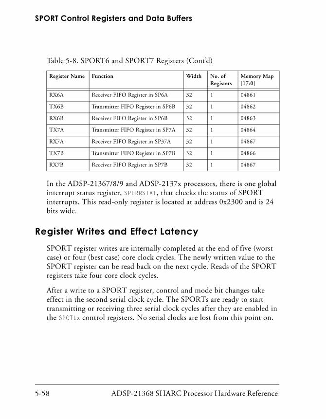
SPORT Control Registers and Data Buffers
5-58 ADSP-21368 SHARC Processor Hardware Reference
In the ADSP-21367/8/9 and ADSP-2137x processors, there is one global interrupt status register, SPERRSTAT, that checks the status of SPORT interrupts. This read-only register is located at address 0x2300 and is 24 bits wide.
Register Writes and Effect LatencySPORT register writes are internally completed at the end of five (worst case) or four (best case) core clock cycles. The newly written value to the SPORT register can be read back on the next cycle. Reads of the SPORT registers take four core clock cycles.
After a write to a SPORT register, control and mode bit changes take effect in the second serial clock cycle. The SPORTs are ready to start transmitting or receiving three serial clock cycles after they are enabled in the SPCTLx control registers. No serial clocks are lost from this point on.
RX6A Receiver FIFO Register in SP6A 32 1 04861
TX6B Transmitter FIFO Register in SP6B 32 1 04862
RX6B Receiver FIFO Register in SP6B 32 1 04863
TX7A Transmitter FIFO Register in SP7A 32 1 04864
RX7A Receiver FIFO Register in SP37A 32 1 04867
TX7B Transmitter FIFO Register in SP7B 32 1 04866
RX7B Receiver FIFO Register in SP7B 32 1 04867
Table 5-8. SPORT6 and SPORT7 Registers (Cont’d)
Register Name Function Width No. of Registers
Memory Map [17:0]

ADSP-21368 SHARC Processor Hardware Reference 5-59
Serial Ports
Serial Port Control Registers (SPCTLx)The main control registers for each SPORT are the SPORT control regis-ters, SPCTLx. These registers are described in “SPORT Serial Control Registers (SPCTLx)” on page A-29. When changing operating modes, clear the SPORT control registers before the new mode is written to the registers.
There is one global control and status register for each SPORT (unlike previous SHARC designs where SPORTs were paired) for multichannel operation. These registers are SPMCTL0–7 and they define the number of channels, provide the status of the current channel, enable multichannel operation, and set the multichannel frame delay. These registers are described in “SPORT Multichannel Control Registers (SPMCTLx)” on page A-40.
The SPCTLx registers control the operating modes of the SPORTs for the I/O processor. Table 5-9 lists all the bits in the SPCTLx registers.
Table 5-9. SPCTLx Control Bit Comparison in Four SPORT Operation Modes
Bit Standard DSP Serial Mode Left-justified and I2S Mode Multichannel Mode
0 SPEN_A SPEN_A Reserved
1 DTYPE Reserved DTYPE
2 DTYPE Reserved DTYPE
3 LSBF Reserved LSBF
4 SLEN0 SLEN0 SLEN0
5 SLEN1 SLEN1 SLEN1
6 SLEN2 SLEN2 SLEN2
7 SLEN3 SLEN3 SLEN3
8 SLEN4 SLEN4 SLEN4
9 PACK PACK PACK

SPORT Control Registers and Data Buffers
5-60 ADSP-21368 SHARC Processor Hardware Reference
10 ICLK MSTR ICLK
11 OPMODE OPMODE OPMODE
12 CKRE Reserved CKRE
13 FSR Reserved Reserved
14 IFS Reserved IMFS
15 DIFS DIFS Reserved
16 LFS FRFS LMFS
17 LAFS LAFS Reserved
18 SDEN_A SDEN_A SDEN_A
19 SCHEN_A SCHEN_A SCHEN_A
20 SDEN_B SDEN_B SDEN_B
21 SCHEN_B SCHEN_B SCHEN_B
22 FS_BOTH No effect Reserved
23 BHD BHD BHD
24 SPEN_B SPEN_B Reserved
25 SPTRAN SPTRAN SPTRAN
26 ROVF_B, or TUVF_B ROVF_B, or TUVF_B DERR_B, ROVF_B, or TUVF_B
27 DXS_B DXS_B DXS_B
28 DXS_B DXS_B DXS_B
29 ROVF_A, or TUVF_A ROVF_A, or TUVF_A DERR_A, ROVF_A, or TUVF_A
30 DXS_A DXS_A DXS_A
31 DXS_A DXS_A DXS_A
Table 5-9. SPCTLx Control Bit Comparison in Four SPORT Operation Modes (Cont’d)
Bit Standard DSP Serial Mode Left-justified and I2S Mode Multichannel Mode
ADSP-21368 SHARC Processor Hardware Reference 5-61
Serial Ports
The following bits, listed in bit number order, control SPORT modes and are part of the SPCTLx (transmit and receive) control registers. Other bits in the SPCTLx registers set up DMA and I/O processor-related SPORT fea-tures. For information about configuring a specific operation mode, refer to Table 5-1 on page 5-11 and “Standard DSP Serial Mode” on page 5-12.
Serial port enable. SPCTLx registers, bits 0 and 24 (SPEN_A and SPEN_B). These bits enable (if set, = 1) or disable (if cleared, = 0) the corresponding SPORT channel A or B. Clearing these bits aborts any ongoing operation and clears the status bits. The SPORTS are ready to transmit or receive two serial clock cycles after enabling. This description applies to I2S, left-justified sample pair, and DSP standard serial modes only.
Data type select. SPCTLx registers, bits 2–1 (DTYPE). These bits select the companding and MSB data type formatting of serial words loaded into the transmit and receive buffers. These bits applies to DSP standard serial and multichannel modes only. The transmit shift register does not zero-fill or sign-extend transmit data words; this only takes place for the receive shift register.
For standard mode, selection of companding mode and MSB format are exclusive:
00 = Right-justify; fill unused MSBs with 0s01 = Right-justify; sign-extend into unused MSBs10 = Compand using μ_law, (primary channels only)11 = Compand using A_law, (primary channels only)
For multichannel mode, selection of companding mode and MSB format are independent:
x0 = Right-justify; fill unused MSBs with 0sx1 = Right-justify; sign-extend into unused MSBs0x = Compand using μ_law 1x = Compand using A_law

SPORT Control Registers and Data Buffers
5-62 ADSP-21368 SHARC Processor Hardware Reference
This description applies only to DSP standard serial and multichannel modes only.
Serial word endian select. SPCTLx registers, bit 3 (LSBF). This bit selects little endian words (LSB first, if set, = 1) or big endian words (MSB first, if cleared, = 0). This description applies to DSP standard serial and multi-channel modes only.
Serial word length select. SPCTLx registers, bits 8–4 (SLENx). These bits select the word length in bits. Word sizes can be from 3 bits (SLEN = 2) to 32 bits (SLEN = 31). This bit applies to all operation modes.
Use this formula to calculate the value for SLEN:SLEN = actual serial word length – 1
The SLEN bit cannot equal 0 or 1. I2S, and left-justified sample pair word length is limited to 8-32 bits. DSP standard mode word length varies from 3-32 bits.
16-bit to 32-bit word packing enable. SPCTLx registers, bit 9 (PACK). This bit enables (if set, = 1) or disables (if cleared, = 0) 16- to 32-bit word pack-ing. This bit applies to all operation modes.
Internal clock select. SPCTLx registers, bit 10 (ICLK). This bit selects the internal (if set, = 1) or external (if cleared, = 0) transmit or receive clock. This bit applies to DSP standard serial mode and multichannel modes.
Sport operation mode. SPCTLx registers, bit 11 (OPMODE). This bit enables I2S, left-justified sample pair, and packed I2S in multichannel modes if set (= 1), or disables if cleared (= 0). This bit applies to all operation modes. See Table 5-1 on page 5-11 and “Standard DSP Serial Mode” on page 5-12.
Clock rising edge select. SPCTLx registers, bit 12 (CKRE). This bit selects whether the SPORT uses the rising edge (if set, = 1) or falling edge (if cleared, = 0) of the clock signal for sampling data and the frame sync. This bit applies to DSP standard serial and multichannel modes only.

ADSP-21368 SHARC Processor Hardware Reference 5-63
Serial Ports
Frame sync required select. SPCTLx registers, bit 13 (FSR). This bit selects whether the SPORT requires (if set, = 1) or does not require (if cleared,= 0) a transfer frame sync. See “Frame Sync Options” on page 5-37 for more details. This bit applies to DSP standard serial mode only.
Internal frame sync select. SPCTLx registers, bit 14 (IFS). This bit selects whether the SPORT uses an internally-generated frame sync (if set, = 1) or a frame sync from an external (if cleared, = 0) source. This bit is used for standard DSP serial and multichannel modes only. This bit is referred as IMFS in multichannel mode.
Low active frame sync select. SPCTLx registers, bit 16 (LFS). This bit selects the logic level of the (transmit or receive) frame sync signals. This bit selects an active low frame sync (if set, = 1) or active high frame sync (if cleared, = 0). Active high is the default. This bit is called FRFS in I2S and left-justified modes and LTDV/LMFS in multichannel mode.
Late frame sync select. SPCTLx registers, bit 17 (LAFS). This bit selects when to generate the frame sync signal. This bit selects a late frame sync if set (= 1) during the first bit of each data word. This bit selects an early frame sync if cleared (= 0) during the serial clock cycle immediately pre-ceding the first data bit. See “Frame Sync Options” on page 5-37 for more details.
This bit applies to DSP standard serial mode only. This bit is also used to select between I2S and left-justified sample pair modes. See Table 5-1 on page 5-11 and “Standard DSP Serial Mode” on page 5-12 for more information.
Serial port DMA enable. SPCTLx registers, bits 18 and 20 (SDEN_A and SDEN_B). These bits enable (if set, = 1) or disable (if cleared, = 0) the SPORT’s channel DMA. Bits 18 and 20 apply to all operating modes.
Serial port DMA chaining enable. SPCTLx registers, bits 19 and 21 (SCHEN_A and SCHEN_B). These bits enable (if set, = 1) or disable (if cleared, = 0) SPORT’s channels A and B DMA chaining. Bits 19 and 21 apply to all operating modes.

SPORT Control Registers and Data Buffers
5-64 ADSP-21368 SHARC Processor Hardware Reference
Frame sync both enable. SPCTLx registers, bit 22 (FS_BOTH). This bit applies when the SPORTs channels A and B are configured to trans-mit/receive data. If set (= 1), this bit issues frame sync only when data is present in both transmit buffers, TXA and TXB. If cleared (= 0), a frame sync is issued if data is present in either transmit buffers. This bit applies to DSP standard serial mode only.
When a SPORT is configured as a receiver, if FS_BOTH is set (= 1), frame sync is issued only when both the Rx FIFOs (RXSPA and RXSPB) are not full.
This bit is not used for I2S and left-justified sample pair modes. If only channel A or channel B is selected, the frame sync behaves as if FS_BOTH is cleared (= 0). If both A and B channels are selected, the word select acts as if FS_BOTH is set (= 1).
Buffer hang disable. SPCTLx registers, bit 23 (BHD). When cleared (= 0), this bit causes the processor core to hang when it attempts to write to a full buffer or read from an empty buffer. When set (= 1), this bit disables the core hang. In this case, a core read from an empty receive buffer returns previously read (invalid) data and core writes to a full transmit buffer to overwrite (valid) data that has not yet been transmitted. This bit is used in all modes.
Data direction control. SPCTLx registers, bit 25 (SPTRAN). This bit controls the data direction of the SPORT channel A and B signals.
When cleared (= 0), the SPORT is configured to receive on both channels A and B. When configured to receive, the RXSPxA and RXSPxB buffers are activated, while the receive shift registers are controlled by SPORTx_CLK and SPORTx_FS. The TXSPxA and TXSPxB buffers are inactive.

ADSP-21368 SHARC Processor Hardware Reference 5-65
Serial Ports
When set (= 1), the SPORT is configured to transmit on both channels A and B. When configured to transmit, the TXSPxA and TXSPxB buffers are activated, while the transmit shift registers are controlled by SPORTx_CLK and SPORTx_FS. The RXSPxA and RXSPxB buffers are inactive. This bit applies to operating modes.
Reading from or writing to inactive buffers cause the core to hang indefinitely until the SPORT is cleared.
Data buffer error status (sticky, read-only). SPCTLx registers, bits 29 and 26 (DERR_A, DERR_B). These bits indicate whether the serial transmit opera-tion has underflowed (if set, = 1 and SPTRAN = 1) or a receive operation has overflowed (if set, = 1 and SPTRAN = 0) in the TXSPxA/RXSPxA and TXSPxB/RXSPxB data buffers.
This description applies to all operating modes. In multichannel modes, corresponding bits (TUVF, ROVF) are used for this function.
When the SPORT is configured as a transmitter, these bits provide trans-mit underflow status. As a transmitter, if FSR = 1, these bits indicate whether the SPORTx_FS signal (from an internal or external source) occurred while the DXS buffer was empty. If FSR = 0, ROVF or TUVF is set whenever the SPORT is required to transmit and the transmit buffer is empty. The SPORTs transmit data whenever they detect a SPORTx_FS signal.
Specifically, the operation of the TUVF bit is:
• 0 = No SPORTx_FS signal occurred while TXSPxA/B buffer is empty.
• 1 = SPORTx_FS signal occurred while TXSPxA/B buffer is empty.
When the SPORT is configured as a receiver, these bits provide receive overflow status. As a receiver, it indicates when the channel has received new data while the RXS_A buffer is full. New data overwrites existing data.

SPORT Control Registers and Data Buffers
5-66 ADSP-21368 SHARC Processor Hardware Reference
Specifically, the operation of the ROVF bit is:
• 0 = No new data while RXSPxA/B buffer is full.
• 1 = New data while RXSPxA/B buffer is full.
When the DIFS bit is cleared (the default setting), the frame sync signal (SPORTx_FS) is dependent upon new data being present in the transmit buffer. The SPORTx_FS signal is only generated for new data. Setting DIFS to 1 selects data-independent frame syncs which causes the SPORTx_FS sig-nal to be generated whether or not new data is present. With each SPORTx_FS signal, the SPORT transmits the contents of the transmit buffer. Serial port DMA typically keeps the transmit buffer full. The DIFS bit is not applicable for multichannel mode.
In the ADSP-21367/8/9 and ADSP-2137x processors, programs no longer need to poll these registers to detect an underflow or overflow condition. Instead, an interrupt is generated and pro-grams only need to read the new SPORT error status register (SPERRSTAT) to determine what register contains the error and what the error is. For more information, see “Frame Sync Error Detec-tion” on page 5-42.
Data buffer status. SPCTLx registers, bits 31–30 (DXS_A) and bits 28-27 (DXS_B). These read-only bits indicate the status of the SPORT’s data buffer as follows: 11 = buffer full, 00 = buffer empty, 10 = buffer partially full, 01 = reserved.
The DXS_A or DXS_B status bits indicate whether the TXSPxA/RXSPxA or TXSPxB/RXSPxB buffer is full (11), empty (00), or partially full (10). To test for space in TXSPxA/B or RXSPxA/B, test whether DXS_A (bit 30) is equal to zero for the A channel, or whether DXS_B (bit 27) is equal to zero for the B channel. To test for the presence of any data in TXSPxA/B or RXSPxA/B, test whether DXS_A (bit 31) is equal to one for the A channel, or whether DXS_B (bit 28) is equal to one for the B channel. This description applies to all operating modes.

ADSP-21368 SHARC Processor Hardware Reference 5-67
Serial Ports
When the SPORT is configured as a transmitter, these bits reflect transmit buffer status for the TXSPxA and TXSPxB buffers. When the SPORT is configured as a receiver, these bits reflect receive buffer status for the RXSPxA and RXSPxB buffers.
Transmit and Receive Data Buffers (TXSPxA/B, RXSPxA/B)
The transmit buffers (TXSP0A–TXSP7A and TXSP0B–TXSP7B) are the 32-bit transmit data buffers for SPORT0 through SPORT7 respectively. These buffers must be loaded with the data to be transmitted if the SPORT is configured to transmit on the A and B channels. The data is loaded auto-matically by the DMA controller or loaded manually by the program running on the processor core.
The receive buffers (RXSP0A–RXSP7A and RXSP0B–RXSP7B) are the 32-bit receive data buffers for SPORT0 through SPORT7 respectively. These 32-bit buffers become active when the SPORT is configured to receive data on the A and B channels. When a SPORT is configured as a receiver, the RXSPxA and RXSPxB registers are automatically loaded from the receive shifter when a complete word has been received. The data is then loaded to internal memory by the DMA controller or read directly by the pro-gram running on the processor core.
Word lengths of less than 32 bits are automatically right-justified in the receive and transmit buffers.
The transmit buffers act like a two-location FIFO because they have a data register plus an output shift register. Two 32-bit words may both be stored in the transmit queue at any one time. When the transmit register is loaded and any previous word has been transmitted, the register contents are automatically loaded into the output shifter. An interrupt occurs when the output transmit shifter has been loaded, signifying that the transmit

SPORT Control Registers and Data Buffers
5-68 ADSP-21368 SHARC Processor Hardware Reference
buffer is ready to accept the next word (for example, the transmit buffer is not full). This interrupt does not occur when SPORT DMA is enabled or when the corresponding mask bit in the LIRPTL/IRPTL register is set.
When the SPORT is configured as a transmitter (SPTRAN =1) and a trans-mit frame sync occurs and no new data has been loaded into the transmit buffer, a transmit underflow status bit is set in the SPORT control regis-ters. The TUVF_A/ROVF_A or TUVF_A status bit is sticky and is only cleared by disabling the SPORT.
When the SPORT is configured as a receiver (SPTRAN = 0), the receive buffers are activated. The receive buffers act like a three-location FIFO because they have two data registers plus an input shift register. Two com-plete 32-bit words can be stored in the receive buffer while a third word is shifted in. The third word overwrites the second if the first word has not been read out (by the processor core or the DMA controller). When this happens, the receive overflow status bit is set in the SPORT control regis-ters. Almost three complete words can be received without the receive buffer being read before an overflow occurs. The overflow status is gener-ated on the last bit of the third word. The ROVF_A/ROVF_A or TUVF_A status bit is sticky and is cleared only by disabling the SPORT.
An interrupt is generated when the receive buffer is loaded with a received word (for example, the receive buffer is not empty). This interrupt is masked if SPORT DMA is enabled or if the corresponding bit in the LIRPTL register is set.
If your program causes the core processor to attempt to read from an empty receive buffer or to write to a full transmit buffer, the access is delayed until the buffer is accessed by the external I/O device. This delay is called a core processor hang. In order to access the receive or transmit buffer without a hang, read the buffer’s status to determine whether the access can be made.

ADSP-21368 SHARC Processor Hardware Reference 5-69
Serial Ports
To support debugging buffer transfers, the ADSP-21367/8/9 and ADSP-2137x processors have a buffer hang disable (BHD) bit. When set (= 1), this bit prevents the processor core from detecting a buffer-related stall condition, permitting debugging of this type of stall condition. For more information, see the BHD bit description on on page 5-64.
The status bits in SPCTLx are updated during reads and writes from the core processor even when the SPORT is disabled. Disable the SPORT when writing to the receive buffer or reading from the transmit buffer.
When programming the SPORT channel (A or B) as a transmitter, only the corresponding TXSPxA and TXSPxB buffers become active while the receive buffers RXSPxA and RXSPxB remain inactive. Simi-larly, when the SPORT channel A and B are programmed as receive-only, the corresponding RXSPxA and RXSPxB are activated. Do not attempt to read or write to inactive data buffers. If the pro-cessor operates on the inactive transmit or receive buffers while the SPORT is enabled, unpredictable results may occur.
Clock and Frame Sync Frequency Registers (DIVx)The DIVx registers contain divisor values that determine frequencies for internally-generated clocks and frame syncs. The DIVx registers are described in Appendix A in “SPORT Divisor Registers (DIVx)” on page A-44 and are shown in Figure 5-10.
The CLKDIV bit field specifies how many times the processor’s internal clock (CCLK) is divided to generate the transmit and receive clocks. The frame sync (SPORTx_FS) is considered a receive frame sync if the data sig-nals are configured as receivers. Likewise, the frame sync SPORTx_FS is considered a transmit frame sync if the data signals are configured as

SPORT Control Registers and Data Buffers
5-70 ADSP-21368 SHARC Processor Hardware Reference
transmitters. The divisor is a 15-bit value, allowing a wide range of serial clock rates. Use the following equation to calculate the serial clock frequency:
The maximum serial clock frequency is equal to one-eighth the processor’s internal clock (CCLK) frequency, which occurs when CLKDIV is set to zero. Use the following equation to determine the value of CLKDIV, given the CCLK frequency and desired serial clock frequency:
The FSDIV bit field specifies how many transmit or receive clock cycles are counted before a frame sync pulse is generated. In this way, a frame sync can initiate periodic transfers. The counting of serial clock cycles applies to internally- or externally-generated serial clocks. The formula for the number of cycles between frame sync pulses is:
# of serial clocks between frame syncs = FSDIV + 1
Figure 5-10. DIVx Register
fSPORTx_CLK
fCCLK8 CLKDIV 1+( )---------------------------------------=
CLKDIVfCCLK
8 fSPORTx_CLK( )---------------------------------- 1–=
31 30 29 28 27 26 24 23 22 21 20 19 18 17 16
00 0 0 0 0 0 0 0 0 0 0 0 0 0 0
FSDIV
15 14 13 12 11 10 8 7 6 5 4 3 2 1 0
00 0 0 0 0 0 0 0 0 0 0 0 0 0 0
CLKDIVClock Divisor
25
9
Frame Sync Divisor
Reserved
DIV0 (0xC02)DIV1 (0xC03)DIV2 (0x402)DIV3 (0x403)DIV4 (0x4802)DIV5 (0x4803)

ADSP-21368 SHARC Processor Hardware Reference 5-71
Serial Ports
Use the following equation to determine the value of FSDIV, given the serial clock frequency and desired frame sync frequency:
The frame sync is continuously active when FSDIV = 0. The value of FSDIV should not be less than the serial word length minus one (the value of the SLEN field in the SPORT control registers), as this may cause an external device to abort the current operation or cause other unpredictable results. If the SPORT is not being used, the FSDIV divisor can be used as a counter for dividing an external clock or for generating a periodic pulse or periodic interrupt. The SPORT must be enabled for this mode of operation to work properly.
Exercise caution when operating with externally-generated transmit clocks near the frequency of one-eighth of the processor’s internal clock. There is a delay between when the clock arrives at the SPORTx_CLK node and when data is output. This delay may limit the receiver’s speed of operation. Refer to the product-specific data sheet for exact timing specifications.
Externally-generated late transmit frame syncs also experience a delay from when they arrive to when data is output. This can also limit the max-imum serial clock speed. Refer to the product-specific data sheet for exact timing specifications.
SPORT ResetThere are two ways to reset the SPORTs, via software or hardware. Each method has a different effect on the SPORT.
FSDIVfSPORTx_CLK
fSPORTx_FS---------------------------- 1–=

SPORT Control Registers and Data Buffers
5-72 ADSP-21368 SHARC Processor Hardware Reference
A software reset of the SPEN_A or SPEN_B enable bit disables the SPORT(s) and aborts any ongoing operations. Status bits are also cleared. The SPORTs are ready to start transmitting or receiving data two serial clock cycles after they are enabled in the SPCTLx registers. No serial clocks are lost from this point on.
A hardware reset (RESET) disables the entire processor, including the SPORTs, by clearing the SPCTLx registers. Any ongoing operations are aborted.
SPORT InterruptsEach SPORT has an interrupt associated with it. For each SPORT, both the A and B channel transmit and receive data buffers share the same interrupt vector. The interrupts can be used to indicate the completion of the transfer of a block of serial data when the SPORTs are configured for DMA. They can also be used to perform single word transfers (refer to “Single Word Transfers” on page 5-81). The priority of the SPORT inter-rupts is shown in Table 5-10.
Table 5-10. Priority of the Serial Port Interrupts
Interrupt Name1
1 The interrupt names are defined in the def21367.h file supplied with the ADSP-21xxx DSP development software.
Interrupt
SP1I SPORT1 DMA Channels (Highest Priority)
SP3I SPORT3 DMA Channels
SP5I SPORT5 DMA Channels
SP0I SPORT0 DMA Channels
SP2I SPORT2 DMA Channels
SP4I SPORT4 DMA Channels
SP6I SPORT6 DMA Channels
SP7I SPORT7 DMA Channels

ADSP-21368 SHARC Processor Hardware Reference 5-73
Serial Ports
SPORT interrupts occur on the second system clock (CLKIN) after the last bit of the serial word is latched in or driven out.
Moving Data Between SPORTs and Internal Memory
Transmit and receive data can be transferred between the SPORTs and on-chip memory with single word transfers or with DMA block transfers. Both methods are interrupt-driven, and use the same internally-generated interrupts.
SPORT DMA provides a mechanism for receiving or transmitting an entire block of serial data before the interrupt is generated. When SPORT DMA is not enabled, the SPORT generates an interrupt every time it receives or starts to transmit a data word. The processor’s on-chip DMA controller handles the DMA transfer, allowing the processor core to continue running until the entire block of data is transmitted or received. Service routines can then operate on the block of data rather than on sin-gle words, significantly reducing overhead.
DMA Block TransfersThe DSP’s on-chip DMA controller allows automatic DMA transfers between internal memory and each of the two channels of each SPORT. Each SPORT has two channels for transferring data, and each can be con-figured to receive or to transmit. There are twelve DMA channels for SPORT operations. The SPORT DMA channels are numbered as shown in Table 5-11.

Moving Data Between SPORTs and Internal Memory
5-74 ADSP-21368 SHARC Processor Hardware Reference
Data-direction programmability is supported in standard DSP standard serial, left-justified sample pair, and I2S modes. The value of the SPTRAN bit in SPCTLx (0 = RX, 1 = TX) determines whether the receive or transmit register for the SPORT becomes active.
The SPORT DMA channels are assigned higher priority than all other DMA channels (for example, the SPI port) because of their relatively low service rate and their inability to hold off incoming data. Having a higher priority causes the SPORT DMA transfers to perform first when multiple DMA requests occur in the same cycle.
Table 5-11. Serial Port DMA Channels
Channel Data Buffer Description Priority
0 RXSP1A/TXSP1A SPORT1 A data Highest
1 RXSP1B/TXSP1B SPORT1 B data
2 RXSP0A/TXSP0A SPORT0 A data
3 RXSP0B/TXSP0B SPORT0 B data
4 RXSP3A/TXSP3A SPORT3 A data
5 RXSP3B/TXSP3B SPORT3 B data
6 RXSP2A/TXSP2A SPORT2 A data
7 RXSP2B/TXSP2B SPORT2 B data
8 RXSP5A/TXSP5A SPORT5 A data
9 RXSP5B/TXSP5B SPORT5 B data
10 RXSP4A/TXSP4A SPORT4 A data
11 RXSP4B/TXSP4B SPORT4 B data
12 RXSP7A/TXSP7A SPORT7 A data
13 RXSP7B/TXSP7B SPORT7 B data
14 RXSP6A/TXSP6A SPORT6 A data
15 RXSP6B/TXSP6B SPORT6 B data Lowest

ADSP-21368 SHARC Processor Hardware Reference 5-75
Serial Ports
Although the DMA transfers are performed with 32-bit words, SPORTs can handle word sizes from 3 to 32 bits, with 8 to 32 bits for I2S mode. If serial words are 16 bits or smaller, they can be packed into 32-bit words for each DMA transfer. DMA transfers are configured using the PACK bit in the SPCTLx registers. When SPORT data packing is enabled (PACK = 1), the transmit and receive interrupts are generated for the 32-bit packed words, not for each 16-bit word.
The following sections present an overview of SPORT DMA operations; additional details are covered in the “Memory” chapter in the ADSP-2136x SHARC Processor Programming Reference.
• For information on SPORT DMA channel setup, see “Setting Up DMA on SPORT Channels” on page 5-75.
• For information on SPORT DMA parameter registers, see “SPORT DMA Parameter Registers” on page 5-76.
• For information on SPORT DMA chaining, see “SPORT DMA Chaining” on page 5-81.
Setting Up DMA on SPORT Channels
Each SPORT DMA channel has an enable bit (SDEN_A and SDEN_B) in its SPCTLx registers. When DMA is disabled for a particular channel, the SPORT generates an interrupt every time it receives a data word or when-ever there is a vacancy in the transmit buffer. For more information, see “Single Word Transfers” on page 5-81.
Each channel also has a DMA chaining enable bit (SCHEN_A and SCHEN_B) in its SPCTLx registers.
To set up a SPORT DMA channel, write a set of memory buffer parame-ters to the SPORT DMA parameter registers as shown in Table 5-12.

Moving Data Between SPORTs and Internal Memory
5-76 ADSP-21368 SHARC Processor Hardware Reference
Load the II, IM, and C registers with a starting address for the buffer, an address modifier, and a word count, respectively. These registers can be written from the core processor.
Once SPORT DMA is enabled, the processor’s DMA controller automat-ically transfers received data words in the receive buffer to the buffer in internal memory. Likewise, when the SPORT is ready to transmit data, the DMA controller automatically transfers a word from internal memory to the transmit buffer. The controller continues these transfers until the entire data buffer is received or transmitted.
When the count register of an active DMA channel reaches zero, the SPORT generates the corresponding interrupt.
SPORT DMA Parameter RegistersA DMA channel consists of a set of parameter registers that implements a data buffer in internal memory and the hardware the SPORT uses to request DMA service. The parameter registers for each SPORT DMA channel and their addresses are shown in Table 5-13. These registers are part of the processor’s memory-mapped IOP register set.
Table 5-12. SPORT DMA Parameter Registers
Register (Y = A or B, and x = 0 – 5)
Width Description
IISPxy 19 bits DMA channel; x index; start address for data buffer
IMSPxy 16 bits DMA channel; x modify; address increment
CSPxy 16 bits DMA channel; x count; number of words to transmit
CPSPxy 20 bits DMA channel; x chain pointer; address containing the next set of data buffer parameters

ADSP-21368 SHARC Processor Hardware Reference 5-77
Serial Ports
The DMA channels operate similarly to the processor’s data address gen-erators (DAGs). Each channel has an index register (IISPxy) and a modify register (IMSPxy) for setting up a data buffer in internal memory. It is nec-essary to initialize the index register with the starting address of the data buffer. After it transfers each serial I/O word to (or from) the SPORT, the DMA controller adds the modify value to the index register to generate the address for the next DMA transfer. The modify value in the IM register is a signed integer, which provides capability for both incrementing and decrementing the buffer pointer.
Each DMA channel has a count register (CSPxA/CSPxB) which must be ini-tialized with a word count that specifies the number of words to transfer. The count register decrements after each DMA transfer on the channel. When the word count reaches zero, the SPORT generates an interrupt, then automatically disables the DMA channel.
Each SPORT DMA channel also has a chain pointer register (CPSPxy). The CPSPxy register functions are used in chained DMA operations. For more information on SPORT DMA chaining registers, see Table 5-12 on page 5-76.
Table 5-13. SPORT DMA Parameter Registers Addresses
Register Address DMA Channel SPORT Buffer
IISP0A 0xC40 0 RXSP0A or TXSP0A
IMSP0A 0xC41 0 RXSP0A or TXSP0A
CSP0A 0xC42 0 RXSP0A or TXSP0A
CPSP0A 0xC43 0 RXSP0A or TXSP0A
IISP0B 0xC44 1 RXSP0B or TXSP0B
IMSP0B 0xC45 1 RXSP0B or TXSP0B
CSP0B 0xC46 1 RXSP0B or TXSP0B
CPSP0B 0xC47 1 RXSP0B or TXSP0B
IISP1A 0xC48 2 RXSP1A or TXSP1A

Moving Data Between SPORTs and Internal Memory
5-78 ADSP-21368 SHARC Processor Hardware Reference
IMSP1A 0xC49 2 RXSP1A or TXSP1A
CSP1A 0xC4A 2 RXSP1A or TXSP1A
CPSP1A 0xC4B 2 RXSP1A or TXSP1A
IISP1B 0xC4C 3 RXSP1B or TXSP1B
IMSP1B 0xC4D 3 RXSP1B or TXSP1B
CSP1B 0xC4E 3 RXSP1B or TXSP1B
CPSP1B 0xC4F 3 RXSP1B or TXSP1B
Reserved
IISP2A 0x440 4 RXSP2A or TXSP2A
IMSP2A 0x441 4 RXSP2A or TXSP2A
CSP2A 0x442 4 RXSP2A or TXSP2A
CPSP2A 0x443 4 RXSP2A or TXSP2A
IISP2B 0x444 5 RXSP2B or TXSP2B
IMSP2B 0x445 5 RXSP2B or TXSP2B
CSP2B 0x446 5 RXSP2B or TXSP2B
CPSP2B 0x447 5 RXSP2B or TXSP2B
IISP3A 0x448 6 RXSP3A or TXSP3A
IMSP3A 0x449 6 RXSP3A or TXSP3A
CSP3A 0x44A 6 RXSP3A or TXSP3A
CPSP3A 0x44B 6 RXSP3A or TXSP3A
IISP3B 0x44C 7 RXSP3B or TXSP3B
IMSP3B 0x44D 7 RXSP3B or TXSP3B
CSP3B 0x44E 7 RXSP3B or TXSP3B
CPSP3B 0x44F 7 RXSP3B or TXSP3B
Table 5-13. SPORT DMA Parameter Registers Addresses (Cont’d)
Register Address DMA Channel SPORT Buffer

ADSP-21368 SHARC Processor Hardware Reference 5-79
Serial Ports
Reserved
IISP4A 0x840 8 RXSP4A or TXSP4A
IMSP4A 0x841 8 RXSP4A or TXSP4A
CSP4A 0x842 8 RXSP4A or TXSP4A
CPSP4A 0x843 8 RXSP4A or TXSP4A
IISP4B 0x844 9 RXSP4B or TXSP4B
IMSP4B 0x845 9 RXSP4B or TXSP4B
CSP4B 0x846 9 RXSP4B or TXSP4B
CPSP4B 0x847 9 RXSP4B or TXSP4B
IISP5A 0x848 10 RXSP5A or TXSP5A
IMSP5A 0x849 10 RXSP5A or TXSP5A
CSP5A 0x84A 10 RXSP5A or TXSP5A
CPSP5A 0x84B 10 RXSP5A or TXSP5A
IISP5B 0x84C 11 RXSP5B or TXSP5B
IMSP5B 0x84D 11 RXSP5B or TXSP5B
CSP5B 0x84E 11 RXSP5B or TXSP5B
CPSP5B 0x84F 11 RXSP5B or TXSP5B
IISP6A 0x4840 12 RXSP6A or TXSP6A
IMSP6A 0x4841 12 RXSP6A or TXSP6A
CSP6A 0x4842 12 RXSP6A or TXSP6A
CPSP6A 0x4843 12 RXSP6A or TXSP6A
IISP6B 0x4844 13 RXSP6B or TXSP6B
IMSP6B 0x4845 13 RXSP6B or TXSP6B
CSP6B 0x4846 13 RXSP6B or TXSP6B
Table 5-13. SPORT DMA Parameter Registers Addresses (Cont’d)
Register Address DMA Channel SPORT Buffer
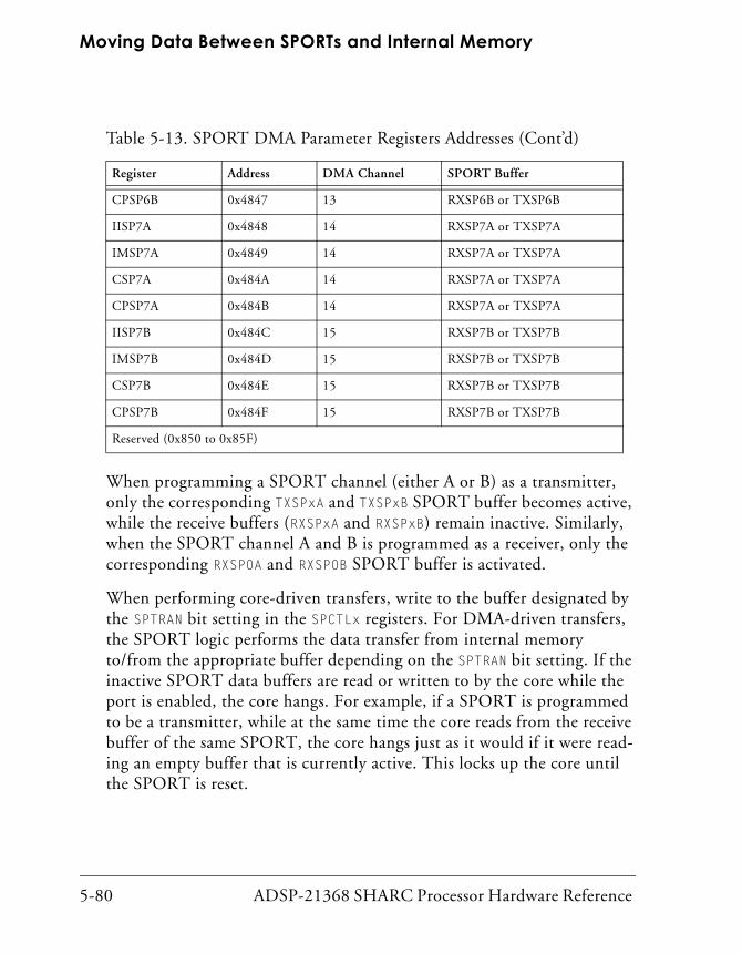
Moving Data Between SPORTs and Internal Memory
5-80 ADSP-21368 SHARC Processor Hardware Reference
When programming a SPORT channel (either A or B) as a transmitter, only the corresponding TXSPxA and TXSPxB SPORT buffer becomes active, while the receive buffers (RXSPxA and RXSPxB) remain inactive. Similarly, when the SPORT channel A and B is programmed as a receiver, only the corresponding RXSP0A and RXSP0B SPORT buffer is activated.
When performing core-driven transfers, write to the buffer designated by the SPTRAN bit setting in the SPCTLx registers. For DMA-driven transfers, the SPORT logic performs the data transfer from internal memory to/from the appropriate buffer depending on the SPTRAN bit setting. If the inactive SPORT data buffers are read or written to by the core while the port is enabled, the core hangs. For example, if a SPORT is programmed to be a transmitter, while at the same time the core reads from the receive buffer of the same SPORT, the core hangs just as it would if it were read-ing an empty buffer that is currently active. This locks up the core until the SPORT is reset.
CPSP6B 0x4847 13 RXSP6B or TXSP6B
IISP7A 0x4848 14 RXSP7A or TXSP7A
IMSP7A 0x4849 14 RXSP7A or TXSP7A
CSP7A 0x484A 14 RXSP7A or TXSP7A
CPSP7A 0x484B 14 RXSP7A or TXSP7A
IISP7B 0x484C 15 RXSP7B or TXSP7B
IMSP7B 0x484D 15 RXSP7B or TXSP7B
CSP7B 0x484E 15 RXSP7B or TXSP7B
CPSP7B 0x484F 15 RXSP7B or TXSP7B
Reserved (0x850 to 0x85F)
Table 5-13. SPORT DMA Parameter Registers Addresses (Cont’d)
Register Address DMA Channel SPORT Buffer

ADSP-21368 SHARC Processor Hardware Reference 5-81
Serial Ports
Therefore, set the direction bit, the SPORT enable bit, and DMA enable bits before initiating any operations on the SPORT data buffers. If the processor operates on the inactive transmit or receive buffers while the SPORT is enabled, it can cause unpredictable results.
SPORT DMA Chaining
In chained DMA operations, the processor’s DMA controller automati-cally sets up another DMA transfer when the contents of the current buffer are transmitted (or received). The chain pointer registers (CPSPxy) function as a pointer to the next set of buffer parameters stored in mem-ory. The DMA controller automatically downloads these buffer parameters to set up the next DMA sequence. For more information on SPORT DMA chaining, see “Setting Up DMA Parameter Registers” on page 2-24.
DMA chaining occurs independently for the transmit and receive channels of each SPORT. Each SPORT DMA channel has a chaining enable bit (SCHEN_A or SCHEN_B) that when set (= 1) enables DMA chaining and when cleared (= 0) disables DMA chaining. Writing all zeros to the address field of the chain pointer registers (CPSPxy) also disables chaining.
Single Word TransfersIndividual data words may also be transmitted and received by the SPORTs, with interrupts occurring as each 32-bit word is transmitted or received. When a SPORT is enabled and DMA is disabled, the SPORT interrupts are generated whenever a complete 32-bit word has been received in the receive buffer, or whenever the transmit buffer is not full. Note that both channel A and B buffers share the same interrupt vector. Single word interrupts can be used to implement interrupt-driven I/O on the SPORTs.

SPORT Programming Examples
5-82 ADSP-21368 SHARC Processor Hardware Reference
To avoid hanging the processor core, check the buffer’s full/empty status when the processor core’s program reads a word from a SPORT’s receive buffer or writes a word to its transmit buffer. The full/empty status can be read in the DXS bits of the SPCTLx registers. Reading from an empty receive buffer or writing to a full transmit buffer causes the processor to hang, while it waits for the status to change.
To support debugging buffer transfers, the processor has a buffer hang disable (BHD) bit. When set (= 1), this bit prevents the proces-sor core from detecting a buffer-related stall condition, permitting debugging of this type of stall condition. For more information, see the BHD bit discussion on on page 5-64.
Multiple interrupts can occur if both SPORTs transmit or receive data in the same cycle. Any interrupt can be masked in the IMASK register; if the interrupt is later enabled in the LIRPTL register, the corresponding inter-rupt latch bit in the IRPTL or LIRPTL registers must be cleared in case the interrupt has occurred in the same time period.
When SPORT data packing is enabled (PACK = 1 in the SPCTLx control registers), the transmit and receive interrupts are generated for 32-bit packed words, not for each 16-bit word.
SPORT Programming ExamplesThis section provides three programming examples written for the ADSP-21367/8/9 and ADSP-2137x processors. The first, Listing 5-1, transmits a buffer of data from SPORT5 to SPORT4 using DMA and the internal loopback feature of the SPORT. In this example, SPORT5 drives the clock and frame sync, and the buffer is transferred only one time.
The second listing, Listing 5-2, transmits a buffer of data from SPORT2 to SPORT3 using direct core reads and writes and the internal loopback feature of the SPORT. In this example, SPORT2 drives the clock and frame sync, and the buffer is transferred only one time.

ADSP-21368 SHARC Processor Hardware Reference 5-83
Serial Ports
The third listing, Listing 5-3, transmits a buffer of data from SPORT1 to SPORT0 using DMA chaining and the internal loopback feature of the SPORT. In this example, SPORT5 drives the clock and frame sync, and the two TCBs for each SPORT are set up to ping-pong back and forth to con-tinually send and receive data.
Listing 5-1. SPORT Transmit Using DMA Chaining
/* SPORT DMA Parameter Registers */
#define IISP4A 0x840
#define IISP5A 0x848
#define IMSP4A 0x841
#define IMSP5A 0x849
#define CSP4A 0x842
#define CSP5A 0x84A
/* SPORT Control Registers */
#define DIV4 0x802
#define DIV5 0x803
#define SPCTL4 0x800
#define SPCTL5 0x801
#define SPMCTL4 0x804
/* SPMCTL Bits */
#define SPL 0x00001000
/* SPCTL Bits */
#define SPEN_A 0x00000001
#define SDEN_A 0x00040000
#define SLEN32 0x000001F0
#define SPTRAN 0x02000000
#define IFS 0x00004000
#define FSR 0x00002000
#define ICLK 0x00000400

SPORT Programming Examples
5-84 ADSP-21368 SHARC Processor Hardware Reference
/* Default Buffer Length */
#define BUFSIZE 10
.SECTION/DM seg_dmda;
/*Transmit buffer*/
.var tx_buf5a[BUFSIZE] = 0x11111111,
0x22222222,
0x33333333,
0x44444444,
0x55555555,
0x66666666,
0x77777777,
0x88888888,
0x99999999,
0xAAAAAAAA;
/*Receive buffer*/
.var rx_buf4a[BUFSIZE];
/* Main code section */
.global _main;
.SECTION/PM seg_pmco;
_main:
/* SPORT Loopback: Use SPORT4 as RX & SPORT5 as TX */
/* initially clear SPORT control register */
r0 = 0x00000000;
dm(SPCTL4) = r0;
dm(SPCTL5) = r0;
dm(SPMCTL4) = r0;
SPORT_DMA_setup:

ADSP-21368 SHARC Processor Hardware Reference 5-85
Serial Ports
/* SPORT 5 Internal DMA memory address */
r0 = tx_buf5a; dm(IISP5A) = r0;
/* SPORT 5 Internal DMA memory access modifier */
r0 = 1; dm(IMSP5A) = r0;
/* SPORT 5 Number of DMA transfers to be done */
r0 = @tx_buf5a; dm(CSP5A) = r0;
/* SPORT 4 Internal DMA memory address */
r0 = rx_buf4a; dm(IISP4A) = r0;
/* SPORT 4 Internal DMA memory access modifier */
r0 = 1; dm(IMSP4A) = r0;
/* SPORT 4 Number of DMA5 transfers to be done */
r0 = @rx_buf4a; dm(CSP4A) = r0;
/* set internal loopback bit for SPORT4 & SPORT5 */
bit set ustat3 SPL;
dm(SPMCTL4) = ustat3;
/* Configure SPORT5 as a transmitter */
/* internally generating clock and frame sync */
/* CLKDIV = [fCCLK(333 MHz)/2 x FSCLK(8.325 MHz)] – 1 = 0x0004 */
/* FSDIV = [FSCLK(8.325 MHz)/TFS(.26 MHz)] – 1 = 31 = 0x001F */
R0 = 0x001F0004; dm(DIV5) = R0;
ustat4 = SPEN_A| /* Enable Channel A */
SLEN32| /* 32-bit word length */
FSR| /* Frame Sync Required */
SPTRAN| /* Transmit on enabled channels */
SDEN_A| /* Enable Channel A DMA */
IFS| /* Internally Generated Frame Sync */
ICLK; /* Internally Generated Clock */
dm(SPCTL5) = ustat4;
/* Configure SPORT4 as a receiver */
/* externally generating clock and frame sync */

SPORT Programming Examples
5-86 ADSP-21368 SHARC Processor Hardware Reference
r0 = 0x0; dm(DIV4) = R0;
ustat3 = SPEN_A| /* Enable Channel A */
SLEN32| /* 32-bit word length */
FSR| /* Frame Sync Required */
SDEN_A; /* Enable Channel A DMA */
dm(SPCTL4) = ustat3;
_main.end: jump (pc,0);
Listing 5-2. SPORT Transmit Using Direct Core Access
/* SPORT Control Registers */
#define TXSP2A 0x460
#define RXSP3A 0x465
#define DIV2 0x402
#define DIV3 0x403
#define SPCTL2 0x400
#define SPCTL3 0x401
#define SPMCTL2 0x404
/* SPMCTL Bits */
#define SPL 0x00001000
/* SPCTL Bits */
#define SPEN_A 0x00000001
#define SDEN_A 0x00040000
#define SLEN32 0x000001F0
#define SPTRAN 0x02000000
#define IFS 0x00004000
#define FSR 0x00002000
#define ICLK 0x00000400
/* Default Buffer Length */
#define BUFSIZE 10

ADSP-21368 SHARC Processor Hardware Reference 5-87
Serial Ports
.SECTION/DM seg_dmda;
/* Transmit Buffer */
.var tx_buf2a[BUFSIZE] = 0x11111111,
0x22222222,
0x33333333,
0x44444444,
0x55555555,
0x66666666,
0x77777777,
0x88888888,
0x99999999,
0xAAAAAAAA;
/* Receive Buffer */
.var rx_buf3a[BUFSIZE];
/* Main code section */
.global _main;
.SECTION/PM seg_pmco;
_main:
//bit set mode1 CBUFEN; /* enable circular buffers */
/* SPORT Loopback: Use SPORT2 as RX & SPORT3 as TX */
/* Initially clear SPORT control registers */
r0 = 0x00000000;
dm(SPCTL2) = r0;
dm(SPCTL3) = r0;
dm(SPMCTL2) = r0;
/* Set up DAG registers */
i4 = tx_buf2a;
m4 = 1;
i12 = rx_buf3a;
m12 = 1;

SPORT Programming Examples
5-88 ADSP-21368 SHARC Processor Hardware Reference
SPORT_DMA_setup:
/* set internal loopback bit for SPORT2 & SPORT3 */
bit set ustat3 SPL;
dm(SPMCTL2) = ustat3;
/* Configure SPORT2 as a transmitter */
/* internally generating clock and frame sync */
/* CLKDIV = [fCCLK(333MHz)/2 x FSCLK(8.325 MHz)] – 1 = 0x0004 */
/* FSDIV = [FSCLK(8.325 MHz)/TFS(.26 MHz)] – 1 = 31 = 0x001F */
R0 = 0x001F0004; dm(DIV2) = R0;
ustat4 = SPEN_A| /* Enable Channel A */
SLEN32| /* 32-bit word length */
FSR| /* Frame Sync Required */
SPTRAN| /* Transmit on enabled channels */
IFS| /* Internally Generated Frame Sync */
ICLK; /* Internally Generated Clock */
dm(SPCTL2) = ustat4;
/* Configure SPORT3 as a receiver */
/* externally generating clock and frame sync */
r0 = 0x0; dm(DIV3) = R0;
ustat3 = SPEN_A| /* Enable Channel A */
SLEN32| /* 32-bit word length */
FSR; /* Frame Sync Required */
dm(SPCTL3) = ustat3;
/* Set up loop to transmit and receive data */
lcntr = LENGTH(tx_buf2a), do (pc,4) until lce;
/* Retrieve data using DAG1 and send TX via SPORT2 */
r0 = dm(i4,m4);
dm(TXSP2A) = r0;
/* Receive data via SPORT3 and save via DAG2 */
r0 = dm(RXSP3A);
pm(i12,m12) = r0;
_main.end: jump (pc,0);

ADSP-21368 SHARC Processor Hardware Reference 5-89
Serial Ports
Listing 5-3. SPORT Transmit Using DMA
/* SPORT DMA Parameter Registers */
#define CPSP0A 0xC43
#define CPSP1A 0xC4B
/* SPORT Control Registers */
#define DIV0 0xC02
#define DIV1 0xC03
#define SPCTL0 0xC00
#define SPCTL1 0xC01
#define SPMCTL0 0xC04
/* SPMCTL Bits */
#define SPL 0x00001000
/* SPCTL Bits */
#define SPEN_A 0x00000001
#define SDEN_A 0x00040000
#define SCHEN_A 0x00080000
#define SLEN32 0x000001F0
#define SPTRAN 0x02000000
#define IFS 0x00004000
#define FSR 0x00002000
#define ICLK 0x00000400
/* Default Buffer Length */
#define BUFSIZE 10
.SECTION/DM seg_dmda;
/* TX Buffers */
.var tx_buf1a[BUFSIZE] = 0x11111111,
0x22222222,
0x33333333,

SPORT Programming Examples
5-90 ADSP-21368 SHARC Processor Hardware Reference
0x44444444,
0x55555555,
0x66666666,
0x77777777,
0x88888888,
0x99999999,
0xAAAAAAAA;
.var tx_buf1b[BUFSIZE] = 0x12345678,
0x23456789,
0x3456789A,
0x456789AB,
0x56789ABC,
0x6789ABCD,
0x789ABCDE,
0x89ABCDEF,
0x9ABCDEF0,
0xABCDEF01;
/* RX Buffers */
.var rx_buf0a[BUFSIZE];
.var rx_buf0b[BUFSIZE];
/* TX Transfer Control Blocks */
.var tx_tcb1[4] = 0,BUFSIZE,1,tx_buf1a;
.var tx_tcb2[4] = 0,BUFSIZE,1,tx_buf1b;
/* RX Transfer Control Blocks */
.var rx_tcb1[4] = 0,BUFSIZE,1,rx_buf0a;
.var rx_tcb2[4] = 0,BUFSIZE,1,rx_buf0b;
/* Main code section */
.global _main;
.SECTION/PM seg_pmco;

ADSP-21368 SHARC Processor Hardware Reference 5-91
Serial Ports
_main:
// SPORT Loopback: Use SPORT0 as RX & SPORT1 as TX //
/* initially clear SPORT control register */
r0 = 0x00000000;
dm(SPCTL0) = r0;
dm(SPCTL1) = r0;
dm(SPMCTL1) = r0;
SPORT_DMA_setup:
/* set internal loopback bit for SPORT0 & SPORT1 */
bit set ustat3 SPL;
dm(SPMCTL1) = ustat3;
/* Configure SPORT1 as a transmitter */
/* internally generating clock and frame sync */
/* CLKDIV = [fCCLK(333 MHz)/8xFSCLK(8.325 MHz)]-1 = 0x0004 */
/* FSDIV = [FSCLK(8.325 MHz)/TFS(.26 MHz)]-1 = 31 = 0x001F */
R0 = 0x001F0004; dm(DIV1) = R0;
ustat4 = SPEN_A| /* Enable Channel A */
SLEN32| /* 32-bit word length */
FSR| /* Frame Sync Required */
SPTRAN| /* Transmit on enabled channels */
SDEN_A| /* Enable Channel A DMA */
SCHEN_A| /* Enable Channel A DMA Chaining */
IFS| /* Internally-generated Frame Sync */
ICLK; /* Internally-generated Clock */
dm(SPCTL1) = ustat4;
/* Configure SPORT0 as a receiver */
/* externally generating clock and frame sync */
r0 = 0x0; dm(DIV0) = R0;
ustat3 = SPEN_A| /* Enable Channel A */

SPORT Programming Examples
5-92 ADSP-21368 SHARC Processor Hardware Reference
SLEN32| /* 32-bit word length */
FSR| /* Frame Sync Required */
SDEN_A| /* Enable Channel A DMA */
SCHEN_A; /* Enable Channel A DMA Chaining */
dm(SPCTL0) = ustat3;
/* Next TCB location for tx_tcb2 is tx_tcb1 */
/* Mask the first 19 bits of the TCB location */
r0 = (tx_tcb1 + 3) & 0x7FFFF;
dm(tx_tcb2) = r0;
/* Next TCB location for rx_tcb2 is rx_tcb1 */
/* Mask the first 19 bits of the TCB location */
r0 = (rx_tcb1 + 3) & 0x7FFFF;
dm(rx_tcb2) = r0;
/* Next TCB location for rx_tcb1 is rx_tcb2 */
/* Mask the first 19 bits of the TCB location */
r0 = (rx_tcb2 + 3) & 0x7FFFF;
dm(rx_tcb1) = r0;
/* Initialize SPORT DMA transfer by writing to the CP reg */
dm(CPSP0A) = r0;
/* Next TCB location for tx_tcb1 is tx_tcb2 */
/* Mask the first 19 bits of the TCB location */
r0 = (tx_tcb2 + 3) & 0x7FFFF;
dm(tx_tcb1) = r0;
/* Initialize SPORT DMA transfer by writing to the CP reg */
dm(CPSP1A) = r0;
_main.end: jump (pc,0);

ADSP-21368 SHARC Processor Hardware Reference 6-1
6 SERIAL PERIPHERAL INTERFACE PORTS
The ADSP-21367/8/9 and ADSP-2137x processors are equipped with two synchronous serial peripheral interface ports that are compatible with the industry-standard serial peripheral interface (SPI). The SPI ports are routed through the digital peripheral interface pins (DPI14–1). At reset, SPI functionality is available on DPI pins 1–8. For more information, see Chapter 4, Digital Audio/Digital Peripheral Interfaces. Each SPI port has its own unique set of control registers (the secondary register set is differ-entiated by a B in the register name as in SPIBAUDB). The SPI ports support communication with a variety of peripheral devices including CODECs, data converters, sample rate converters, S/PDIF or AES/EBU digital audio transmitters and receivers, LCDs, shift registers, microcon-trollers, and FPGA devices with SPI emulation capabilities.
Each SPI port provides the following features and capabilities:
• A simple 4-wire interface consisting of two data pins, a device select pin, and a clock pin
• Full-duplex operation that allows the processor to transmit and receive data simultaneously on the same port
• Special data formats to accommodate little and big endian data, different word lengths, and various packing modes
• Master and slave modes as well as multimaster mode in which the processors can be connected to four other SPI devices
• Open drain outputs to avoid possible driver damage due to data contention and to support multimaster scenarios

Functional Description
6-2 ADSP-21368 SHARC Processor Hardware Reference
• Programmable baud rates, clock polarities, and phases
• Master or slave booting from a master SPI device (“DPI/SRU2 Connection Groups” on page 4-51)
• DMA capability to allow data transfers without core overhead
Functional DescriptionEach SPI port contain its own transmit shift (TXSR, TXSRB) and receive shift (RXSR, RXSRB) registers which are not user accessible. The TXSRx regis-ters serially transmit data and the RXSRx registers receive data synchronously with the SPI clock signal (SPICLK). Figure 6-1 shows a block diagram of the ADSP-21367/8/9 and ADSP-2137x processor’s SPI interface. The data is shifted into or out of the shift registers on two sepa-rate pins: the master in slave out (MISO) pin and the master out slave in (MOSI) pin.
During data transfers, one SPI device acts as the SPI master by controlling the data flow. It does this by generating the SPICLK and asserting the SPI device select signal (SPIDS). The SPI master receives data using the MISO pin and transmits using the MOSI pin. The other SPI device acts as the SPI slave by receiving new data from the master into its RXSRx register using the MOSI pin. It transmits requested data out of the TXSR register using the MISO pin.
Each SPI port contains a dedicated transmit data buffer (TXSPI, TXSPIB) and a receive data buffer (RXSPI, RXSPIB). Data to be transmitted is writ-ten to TXSPIx and then automatically transferred into the TXSR register. Once a full data word is received in the RXSR register, the data is automat-ically transferred into RXSPI, from which the data is read. When the port is in SPI master mode, programmable flag pins provide slave selection. Con-nect these pins to the SPIDS of the slave devices.

ADSP-21368 SHARC Processor Hardware Reference 6-3
Serial Peripheral Interface Ports
Different CPUs or processors can take turns being master, or one master may simultaneously shift data into multiple slaves (broadcast mode). However, only one slave may drive its output to write data back to the master at any given time. This must be enforced in broadcast mode, where several slaves can be selected to receive data from the master, but only one slave can be enabled to send data back to the master.
In a multimaster or multidevice environment where multiple processors are connected through their SPI ports, all MOSI pins are connected together, all MISO pins are connected together, as are the SPICLK pins. The master’s FLAGx pins connect to each of the slave SPI devices in the system
Figure 6-1. SPI Block Diagram
RX SHIFT REGISTER
RXSPIRECEIVE
REGISTER
SPI INTERNALCLOCK
GENERATOR
TXSPITRANSMITREGISTER
32
M M SS
SPI IRQ ORDMA REQUEST
TX SHIFT REGISTERTXSRRXSR
SPI INTERFACE LOGIC
MOSI MISO SPICLK SPIDS FLAGX
DM DATA BUS
PM DATA BUS
I/0 DATA BUS
SPICTL
SPISTAT

SPI Interface Signals
6-4 ADSP-21368 SHARC Processor Hardware Reference
through their SPIDS pins. The SPI ports also provide a mechanism to dis-able the MISO pin for multimaster systems where the slave SHARC processor does not need to transmit any data to the master.
SPI Interface SignalsThe SPI uses a 4-wire protocol to enable full-duplex serial communica-tion. This section describes the signals used to connect the ADSP-21367/8/9 and ADSP-2137x processor’s SPI ports in a system that has multiple devices. Figure 6-2 shows the master-slave connections between two devices.
SPI Clock Signal (SPICLK) The SPICLK signal is the serial peripheral interface clock signal. This con-trol signal is driven by the master and regulates the flow of data bits. The master may transmit data at a variety of baud rates. One data bit is trans-ferred for each SPICLK cycle.
Figure 6-2. Master-Slave Interconnections
ADSP-213xx
SPI-Compatible Master DeviceSPICLKFLAGN
MOSI
TXSR
TXSPI
RXSPI
RXSR
MISO
ADSP-213xx
SPI-Compatible Slave DeviceSPICLKSPIDS
MOSI
TXSR
TXSPI
RXSPI
RXSR
MISO

ADSP-21368 SHARC Processor Hardware Reference 6-5
Serial Peripheral Interface Ports
The SPICLK signal is a gated clock that is active only during data transfers, and only for the duration of the transferred word. The number of active edges is equal to the number of bits driven on the data lines. The clock rate can be as high as one-fourth the peripheral clock rate.1 For master devices, the clock rate is determined by the 15-bit value of the baud rate registers (SPIBAUD, SPIBAUDB). For more information, see “SPI Baud Rate Registers (SPIBAUD, SPIBAUDB)” on page A-60. For slave devices, the value in the SPIBAUDx register is ignored. When the SPI device is a master, SPICLK is an output signal. When the SPI is a slave, SPICLK is an input sig-nal. Slave devices ignore the serial clock if its device select (SPIDS) signal is deasserted (HIGH).
Data is shifted in reference to SPICLK. The data is always shifted out on one edge of the clock (referred to as the active edge) and sampled on the opposite edge of the clock (referred to as the sampling edge). Clock polar-ity and clock phase relative to data are programmable through bit 11 (CLKPL) and bit 10 (CPHASE) in the SPICTLx control registers.
SPICLK Timing
When the processor is configured as an SPI slave, the SPI master must drive an SPICLK signal that conforms with Figure 6-3. For exact timing parameters, please refer to the appropriate data sheet.
The SPIDS lead time (T1), the SPIDS lag time (T2), and the sequential transfer delay time (T3) must always be greater than or equal to one-half the SPICLK period. The minimum time between successive word transfers (T4) is two SPICLK periods. This time period is measured from the last active edge of SPICLK of one word to the first active edge of SPICLK of the next word. This calculation is independent from the configuration of the SPI (CPHASE, SPIMS, and so on).
1 For complete information on device clock signals and timing, see the processor-specific data sheet.

SPI Interface Signals
6-6 ADSP-21368 SHARC Processor Hardware Reference
SPI Slave Select Input (SPIDS)
The SPIDS signal is the serial peripheral interface device select input signal. This active low signal is used to enable a processor that is configured as a slave device. As an input only pin, SPIDS behaves like a chip select, and is driven by the master device for the slave devices. When the processor is the SPI master in a multimaster environment, the SPIDS pin acts as an error signal. In multimaster mode, if the SPIDS input signal of a master is asserted (driven low), a multimaster error condition occurs which means that another device is also trying to be the master device. For a single-mas-ter, multiple-slave configuration, the SPIDS signal of the master device must be tied high, or the SPI port allows this signal to be disabled and used as a GPIO input.
SPI Flag Signals (SPIFLG3-0)These signals are driven by the processor as an SPI master to the SPIDS pin of the slave. When CPHASE = 0, the SPI port hardware controls the device-select signal automatically (determined by the DSxEN bits in the SPIFLG register). Setting CPHASE = 1 requires these signals be manually controlled by the software through the SPIFLGx bits in the SPIFLG and SPIFLGB registers. The SPIFLGx bits are ignored when CPHASE = 0.
Figure 6-3. SPICLK Timing
SPICLKCPHASE =0
T1 T2
T3
T4
SPIDSTO SLAVE

ADSP-21368 SHARC Processor Hardware Reference 6-7
Serial Peripheral Interface Ports
Master Out Slave In (MOSI)The MOSI pin is one of the bidirectional I/O data pins. If the ADSP-21367/8/9 and ADSP-2137x processors are configured as masters, the MOSI pin becomes a data transmit (output) pin. If the processors are configured as slaves, the MOSI pin becomes a data receive (input) pin. In an SPI interconnection, the data is shifted out from the MOSI output pin of the master and shifted into the MOSI input of the slave.
Master In Slave Out (MISO)The MISO pin is one of the bidirectional I/O data pins. If the processor is configured as a master, the MISO pin becomes a data receive (input) pin. If the processor is configured as a slave, the MISO pin becomes a data transmit (output) pin. In an SPI interconnection, the data is shifted out from the MISO output pin of the slave and shifted into the MISO input pin of the master.
Figure 6-4 illustrates how the processor can be used as the slave SPI device. The 8-bit host microcontroller is the SPI master. The processor can be booted through its SPI interface to allow application code and data to be downloaded prior to runtime. When a system is comprised of multi-ple slaves, only one slave is allowed to transmit data back to the master at any given time.
Figure 6-4 also shows an example SPI interface where a processor is the SPI master. When it uses the SPI interface, the processor can be directed to alter the conversion resources, mute the sound, modify the volume, and power down the AD1855 stereo DAC by accessing the control register of the DAC serially.

SPI General Operations
6-8 ADSP-21368 SHARC Processor Hardware Reference
SPI General OperationsThe SPI in the ADSP-21367/8/9 and ADSP-2137x processors can be used in a single master as well as in a multimaster environment. In both of these configurations, every MOSI pin in the SPI system is connected. Like-wise, every MISO pin in the system is on a single node, and every SPICLK pin is connected. SPI transmission and reception are always enabled simultaneously, unless broadcast mode has been selected. In broadcast mode, several slaves can be configured to receive from the master, but only one of the slaves can be in transmit mode. This is done by driving the MISO line, to communicate back with the master. If the transmit or receive is not needed, MISO can be ignored and does not need to be connected. This section describes the clock signals, SPI operation as a master and as a slave, and error generation conditions.
Figure 6-4. SHARC Processor as SPI Master and Slave
8-bit HostMICROCONTROLLER
ADSP-213xx
ADSP-213xx AD1855
SPI SLAVE DEVICE
MASTER DEVICE STEREO 96 KHz DAC
SPICLK
SPIDS
MOSI
MISO
CCLK
CLATCH
DATA
FLAG0
S_SEL
SCLK
MOSI
MISO
SPICLK
MOSI
SHARC Processor as SPI Master
SHARC Processor as SPI Slave

ADSP-21368 SHARC Processor Hardware Reference 6-9
Serial Peripheral Interface Ports
SPI EnableFor slaves, the slave-select input acts like a reset for the internal SPI logic. For this reason, the SPIDS line must be error free. The SPIEN signal can also be used as a software reset of the internal SPI logic. An exception to this is the W1C-type (write 1-to-clear) bits in the SPISTATx (SPI status) registers which remain set if they are already set. For a list of write W1C bits, see Table A-11 on page A-57.
Always clear the W1C-type bits before re-enabling the SPI, as these bits do not get cleared even if SPI is disabled. This can be done by writing 0xFF to the SPISTATx registers. In the case of an MME error, enable the SPI ports after SPIDS is deasserted.
Open Drain Mode (OPD)In a multimaster or multislave SPI system, the data output pins (MOSI and MISO) can be configured to behave as open drain drivers to prevent possi-ble damage to pin drivers due to contention. An external pull-up resistor is required on both the MOSI and MISO pins when this option is selected.
When the OPD bit is set and the SPI ports are configured as masters, the MOSI pin is three-stated when the data driven out on MOSI is logic high. The MOSI pin is not three-stated when the driven data is logic low. A zero is driven on the MOSI pin in this case. Similarly, when OPD is set and the SPI ports are configured as slaves, the MISO pin is three-stated if the data driven out on MISO is logic high.

SPI General Operations
6-10 ADSP-21368 SHARC Processor Hardware Reference
Master Mode OperationWhen the SPI is configured as a master, configure the SPI port and start transfers using the following steps:
1. Before enabling the SPI port, programs should specify which of the slave-select signals to use, setting one or more of the required SPI flag select bits (DSxEN) in the SPIFLGx registers.
2. Write to the SPICTLx and SPIBAUDx registers, enabling the device as a master and configuring the SPI system by specifying the appro-priate word length, transfer format, baud rate, and other necessary information.
When CPHASE is set to 0, the slave-select signals are automatically controlled by the SPI port. When CPHASE = 1, the slave selects are controlled by the core and the user software has to control the pins through the SPIFLGx bits. If CPHASE = 1 (user-controlled, slave-select signals), activate the desired slaves by clearing one or more of the SPI flag bits (SPIFLGx) in the SPIFLGx registers.
3. Initiate the SPI transfer. The trigger mechanism for starting the transfer is dependant upon the TIMOD bits in the SPICTLx registers. See “Master Transfer Preparation” on page 6-18 for details.
The SPI generates the programmed clock pulses on SPICLK. The data is shifted out of MOSI and shifted in from MISO simultaneously. Before starting to shift, the TXSR register is loaded with the contents of the TXSPIx registers. At the end of the transfer, the contents of the RXSR register are loaded into the RXSPIx registers.
With each new transfer initiate command, the SPI continues to send and receive words, according to the SPI transfer mode (TIMOD bit in the SPICTLx registers). See “Master Transfer Preparation” on page 6-18 for more details.

ADSP-21368 SHARC Processor Hardware Reference 6-11
Serial Peripheral Interface Ports
In master mode, if the transmit buffer remains empty, or the receive buffer remains full, the device operates according to the states of the SENDZ and GM bits in the SPICTLx registers.
• If SENDZ = 1 and the transmit buffer is empty, the device repeatedly transmits zeros on the MOSI pin. One word is transmitted for each new transfer initiate command.
• If SENDZ = 0 and the transmit buffer is empty, the device repeatedly transmits the last word it transmitted before the transmit buffer became empty.
• If GM = 1 and the receive buffer is full, the device continues to receive new data from the MISO pin, overwriting the older data in the RXSPI buffer.
• If GM = 0 and the receive buffer is full, the incoming data is dis-carded, and the RXSPI register is not updated.
Slave Mode OperationWhen a device is enabled as a slave (and DMA mode is not selected), the start of a transfer is triggered by a transition of the SPIDS select signal to the active state (LOW) or by the first active edge of the clock (SPICLK), depending on the state of CPHASE.
The following steps illustrate SPI operation in slave mode:
1. Write to the SPICTLx registers making sure that the slave’s configu-ration matches the current SPI master.
2. To prepare for the data transfer, write the data to be transmitted into the TXSPIx registers.

SPI General Operations
6-12 ADSP-21368 SHARC Processor Hardware Reference
Once the SPIDS signal’s falling edge is detected, the slave starts sending and receiving data on active SPICLK edges.
The reception or transmission continues until SPIDS is released. The slave device continues to receive or transmit with each new active SPICLK clock edge while the SPIDS signal is active.
In slave mode, if the transmit buffer remains empty, or the receive buffer remains full, the devices operate according to the states of the SENDZ and GM bits in the SPICTLx registers.
• If SENDZ = 1 and the transmit buffer is empty, the device repeatedly transmits zeros on the MISO pin.
• If SENDZ = 0 and the transmit buffer is empty, the device repeatedly transmits the last word it transmitted before the transmit buffer became empty.
• If GM = 1 and the receive buffer is full, the device continues to receive new data from the MOSI pin, overwriting the older data in the RXSPI buffer.
• If GM = 0 and the receive buffer is full, the incoming data is dis-carded, and the RXSPIx registers are not updated.
Multimaster OperationA multimaster mode is implemented in the processor to allow an SPI sys-tem to transfer mastership from one SPI device to another. In a multidevice SPI configuration, several SPI ports are connected and any one (but only one) can become a master at any given time.
If a processor is a slave and wishes to become the SPI master, it asserts the SPIDS pin for the processor that is currently master and then drives the SPICLK signal. Once the master device receives the SPIDS signal, it is

ADSP-21368 SHARC Processor Hardware Reference 6-13
Serial Peripheral Interface Ports
immediately reconfigured as a slave. In order to safely transition from one master to the other, the SPI port uses open drain outputs for the data pin drivers. This helps to avoid possible damage from data contention.
More information on this topic is described in “Mode Fault Error (MME)” on page 6-35.
SPI Data Transfer OperationsThe following sections provide information on the two methods the pro-cessors use to transfer data—through the core or through DMA.
SPI Operation Using the CoreFor core-driven SPI transfers, the software must read from or write to the RXSPIx and TXSPIx registers respectively to control the transfer. It is important to check the buffer status before reading from or writing to these registers because the core does not hang when it attempts to read from an empty buffer or write to a full buffer. When the core writes to a full buffer, the data that is in that buffer is overwritten and the SPI begins transmitting the new data. Invalid data is obtained when the core reads from an empty buffer.
For a master, when the transmit buffer becomes empty, or the receive buffer becomes full, the SPI device stalls the SPI clock until all the data from the receive buffer is read or it detects that the transmit buffer con-tains a piece of data, depending upon the TIMOD setting in the SPICTL register.
• When a master is configured with TIMOD = 01 and the transmit buffer becomes empty, the SPI device stalls the SPI clock until a piece of data is written to the transmit buffer.

SPI Data Transfer Operations
6-14 ADSP-21368 SHARC Processor Hardware Reference
• When a master is configured with TIMOD = 00 and the receive buffer becomes full the SPI device stalls the SPI clock until all of the data is read from the receive buffer.
SPI Operation Using DMAEach SPI has a single DMA channel associated with it that can be config-ured to support either an SPI transmit or a receive, but not both simultaneously. In addition to the TXSPIx and RXSPIx data buffers, there is a four-word deep DMA FIFO that the SPI ports use to improve the data throughput.
The SPI ports support both master and slave mode DMA. The following sections describe master and slave mode DMA operations, DMA chaining, switching between transmit and receive DMA operations, and processing DMA interrupt errors. The following are guidelines to follow when per-forming DMA transfers over the SPI.
• Do not write to the TXSPIx registers during an active SPI transmit DMA operation because DMA data will be overwritten.
• Similarly, do not read from the RXSPIx registers during active SPI DMA receive operations because DMA data will be overwritten.
• Writes to the TXSPIx registers during an active SPI receive DMA operation are permitted. The RXS register is cleared when the RXSPIx registers are read.
• Reads from the RXSPIx registers are allowed at any time during transmit DMA.
• Interrupts are generated based on DMA events and are configured in the SPIDMACx registers.
In order for a transmit DMA operation to begin, the transmit buffer must initially be empty (TXS = 0). While this is normally the case, this means that the TXSPIx registers should not be used for any purpose other than

ADSP-21368 SHARC Processor Hardware Reference 6-15
Serial Peripheral Interface Ports
SPI transfers. For example, the TXSPIx registers should not be used as a scratch register for temporary data storage. Writing to the TXSPIx registers sets the TXS bit.
When the SPI DMA engine is configured for transmitting:
1. The receive interface cannot generate an interrupt, but the status can be polled.
2. The four-deep FIFO is not available in the receive path.
3. The RXSPIx register is used to receive data.
Similarly, when the SPI DMA engine is configured for receiving,
1. The transmit interface cannot generate an interrupt, but the status can be polled.
2. The four-deep FIFO is not available in the transmit path.
3. The TXSPIx register is used to transmit data.
Master Mode DMA Operation
To configure the SPI port for master mode DMA transfers:
1. Specify which FLAG pins to use as the slave-select signals by setting one or more of the DSxEN bits (bits 3–0) in the SPI flag (SPIFLGx) registers.
2. Enable the device as a master and configure the SPI system by selecting the appropriate word length, transfer format, baud rate, and so on in the SPIBAUDx and SPICTLx registers. The TIMOD field (bits 1–0) in the SPICTLx registers is configured to select transmit or receive with DMA mode (TIMOD = 10).
3. Activate the desired slaves by clearing one or more of the SPI flag bits (SPIFLGx) of SPIFLGx registers if CPHASE = 1.

SPI Data Transfer Operations
6-16 ADSP-21368 SHARC Processor Hardware Reference
4. For a single DMA, define the parameters of the DMA transfer by writing to the IISPIx, IMSPIx, and CSPIx registers. For DMA chaining, also write the chain pointer address to the CPSPIx regis-ters after the other DMA registers. For more information, see “Setting Up and Starting Chained DMA over the SPI” on page 2-42.
5. Write to the SPI DMA configuration registers, (SPIDMACx), to spec-ify the DMA direction (SPIRCV, bit 1) and to enable the SPI DMA engine (SPIDEN, bit 0). If DMA chaining is desired, set (= 1) the SPICHEN bit (bit 4) in the SPIDMACx registers.
To avoid data corruption, enable the SPI port before enabling DMA.
If flags are used as slave selects, programs should activate the flags by clear-ing the flag after the SPICTLx and the SPIBAUDx registers are configured, but before enabling the DMA. When CPHASE = 0, and a program is using DMA, the flags are automatically activated by the SPI ports.
When enabled as a master, the DMA engine transmits or receives data as follows:
1. If the SPI system is configured for transmitting, the DMA engine reads data from memory into the SPI DMA FIFO. Data from the DMA FIFO is loaded into the TXSPIx registers and then into the transmit shift register. This initiates the transfer on the SPI port.
2. If configured to receive, data from the RXSPIx registers is automati-cally loaded into the SPI DMA FIFO and the DMA engine reads data from the SPI DMA FIFO and writes to memory. Finally, the SPI initiates the receive transfer.

ADSP-21368 SHARC Processor Hardware Reference 6-17
Serial Peripheral Interface Ports
3. The SPI generates the SPICLK signal (as specified by CPHASE, SPIBAUD, and other bit settings) and the data is shifted out of MOSI and in from MISO simultaneously.
4. The SPI continues sending or receiving words until the SPI DMA word count register decrements to 0.
If the DMA engine is unable to keep up with the transmit stream during a transmit operation because the IOP requires the IOD (I/O data) bus to service another DMA channel (or for another reason), the SPICLK signal stalls until data is written into the TXSPI register. All aspects of SPI receive operation should be ignored. The data in the RXSPI register is not intended to be used, and the RXS (bits 28–27 and 31–30 in the SPCTLx reg-isters) and SPISTAT bits (26 and 29) should be ignored. The ROVF overrun condition cannot generate an error interrupt in this situation.
If the DMA engine cannot keep up with the receive data stream during receive operations, then SPICLK stalls until data is read from RXSPI. While performing a receive DMA, the processor core assumes the transmit buffer is empty. If SENDZ = 1, the device repeatedly transmits zeros. If SENDZ = 0, it repeatedly transmits the contents of the TXSPI register. The TUNF under-run condition cannot generate an error interrupt in this situation.
For receive DMA in master mode, the SPICLK signal stops only when the FIFO and the RXSPI buffer is full (even if the DMA count is zero). Therefore, the SPICLK signal runs for an additional five word transfers filling junk data in the FIFO and the RXSPIx buffers. This data must be cleared before a new DMA is initiated.
A master SPI DMA sequence may involve back-to-back transmission and/or reception of multiple chained DMA transfers. The SPI controller supports such a sequence with minimal processor core interaction.

SPI Data Transfer Operations
6-18 ADSP-21368 SHARC Processor Hardware Reference
Master Transfer Preparation
When the processor is enabled as a master, the initiation of a transfer is defined by the two bit fields (bits 1–0) of TIMOD in the SPICTLx registers. Based on these two bits and the status of the interface, a new transfer is started upon either a read of the RXSPIx registers or a write to the TXSPIx registers. This is summarized in Table 6-1.
Table 6-1. Transfer Initiation
TIMOD Function Transfer Initiated Upon
Action, Interrupt
00 Transmit and Receive
Initiate new single word transfer upon read of RXSPI and pre-vious transfer completed.
The SPI interrupt is latched in every core clock cycle in which the RXSPI buffer has a word in it.Emptying the RXSPI buffer or disabling the SPI port at the same time (SPIEN = 0) stops the interrupt latch.
01 Transmit and Receive
Initiate new single word transfer upon write to TXSPI and previous transfer completed.
The SPI interrupt is latched in every core clock cycle in which the TXSPI buffer is empty.Writing to the TXSPI buffer or disabling the SPI port at the same time (SPIEN = 0) stops the interrupt latch.
10 Transmit or Receive with DMA
Initiate new multiword transfer upon write to DMA enable bit. Indi-vidual word transfers begin with either a DMA write to TXSPI or a DMA read of RXSPI depending on the direction of the transfer as specified by the SPIRCV bit.
If chaining is disabled, the SPI interrupt is latched in the cycle when the DMA count decrements from 1 to 0. If chaining is enabled, interrupt function is based on the CPI bit in the CP register. If CPI = 0, the SPI interrupt is latched at the end of the DMA sequence. If CPI = 1, then the SPI interrupt is latched after each DMA in the sequence. For more information, see “DMA Transfer Direction” on page 2-24.
11 Reserved

ADSP-21368 SHARC Processor Hardware Reference 6-19
Serial Peripheral Interface Ports
Slave Mode DMA Operation
A slave mode DMA transfer occurs when the SPI port is enabled and con-figured in slave mode, and DMA is enabled. When the SPIDS signal transitions to the low state or when the first active edge of SPICLK is detected, it triggers the start of a transfer.
To configure for slave mode DMA:
1. Write to the SPICTLx registers to make the mode of the serial link the same as the mode that is set up in the SPI master. Configure the TIMOD field to select transmit or receive DMA mode (TIMOD = 10).
2. Define DMA receive (or transmit) transfer parameters by writing to the IISPIx, IMSPIx, and CSPIx registers. For DMA chaining, write the chain pointer address to the CPSPIx registers.
3. Write to the SPIDMACx registers to enable the SPI DMA engine and configure the following:
• A receive access (SPIRCV = 1) or
• A transmit access (SPIRCV = 0)
If DMA chaining is desired, set the SPICHEN bit in the SPIDMACx registers.
Enable the SPI port before enabling DMA to avoid data corruption.

SPI Data Transfer Operations
6-20 ADSP-21368 SHARC Processor Hardware Reference
Slave Transfer Preparation
When enabled as a slave, the device prepares for a new transfer according to the function and actions described in Table 6-1.
The following steps illustrate the SPI receive or transmit DMA sequence in an SPI slave in response to a master command:
1. Once the slave-select input is active, the processor starts receiving and transmitting data on active SPICLK edges. The data for one channel (TX or RX) is automatically transferred from/to memory by the IOP. The function of the other channel is dependant on the GM and SENDZ bits in the SPICTL register.
2. Reception or transmission continues until the SPI DMA word count register transitions from 1 to 0.
3. A number of conditions can occur while the processor is configured for the slave mode:
• If the DMA engine cannot keep up with the receive data stream during receive operations, the receive buffer operates according to the state of the GM bit in the SPICTLx registers.
• If GM = 0 and the DMA buffer is full, the incoming data is discarded and the RXSPIx register is not updated. While per-forming a receive DMA, the transmit buffer is assumed to be empty. If SENDZ = 1, the device repeatedly transmits zeros on the MISO pin. If SENDZ = 0, it repeatedly transmits the contents of the TXSPIx registers.
• If GM = 1 and the DMA buffer is full, the device continues to receive new data from the MOSI pin, overwriting the older data in the DMA buffer.
• If the DMA engine cannot keep up with the transmit data stream during a transmit operation because another DMA engine has been granted the bus (or for another reason), the

ADSP-21368 SHARC Processor Hardware Reference 6-21
Serial Peripheral Interface Ports
transmit port operates according to the state of the SENDZ bit in the SPICTLx registers.
If SENDZ = 1 and the DMA buffer is empty, the device repeatedly transmits zeros on the MISO pin. If SENDZ = 0 and the DMA buffer is empty, it repeatedly transmits the last word it transmitted before the DMA buffer became empty. All aspects of SPI receive operation should be ignored. The data in the RXSPIx registers is not intended to be used, and the RXS and ROVF bits should be ignored. The ROVF overrun condition cannot generate an error interrupt in this situation.
While a DMA transfer is occurring on one channel (TX or RX), the core (based on the RXS and TXS status bits) can transfer data in the other direction.
Changing SPI Configuration
Programs should take the following precautions when changing SPI configurations.
• The SPI configuration must not be changed during a data transfer.
• Change the clock polarity only when no slaves are selected.
• Change the SPI configuration only when SPIEN = 0. For example, if operating as a master in a multislave system, and there are slaves that require different data or clock formats, then the master SPI should be disabled, reconfigured, and then re-enabled. However, when an SPI communication link consists of 1) a single master and a single slave, 2) CPHASE = 1, and 3) the slave’s slave select input is tied low, then the program can change the SPI

SPI Data Transfer Operations
6-22 ADSP-21368 SHARC Processor Hardware Reference
configuration. In this case, the slave is always selected. Data cor-ruption can be avoided by enabling the slave only after configuring both the master and slave devices.
When performing transmit operations with the SPI port, disabling the SPI port prematurely can cause data corruption and/or faulty transmission. Before the program disables the SPI port in order to reconfigure it, the status bits should be polled to ensure that all valid data has been com-pletely transferred. For core-driven transfers, data moves from the TXSPI buffer into a shift register. The following bits should be checked before disabling the SPI port:
1. Wait for the TXSPIx buffers to empty into the shift register. This is done when the TXS bit (bit 3) of the SPISTATx registers becomes zero.
2. Wait for the SPI shift registers to finish shifting out data. This is done when the SPIF bit (bit 0 of SPISTATx registers) becomes one.
3. Disable the SPI ports by setting the SPIEN bit (bit 0) in the SPICTLx registers to zero.
When performing transmit DMA transfers, data moves through a four-deep SPI DMA FIFO, then into the TXSPIx buffers, and finally into the shift register. DMA interrupts are latched when the I/O processor moves the last word from memory to the peripheral. For the SPI, this means that the SPI “DMA complete” interrupt is latched when there are still six words yet to be fully transmitted (four in the FIFO, one in the TXSPIx buffers, and one being shifted out of the shift register). To disable the SPI port after a DMA transmit operation, use the following steps:
1. Wait for DMA FIFO to empty. This is done when the SPISx bits (bits 13–12 in the SPIDMACx registers) become zero.
2. Wait for the TXSPIx registers to empty. This is done when the TXS bit (bit 3) in the SPISTATx registers) becomes zero.

ADSP-21368 SHARC Processor Hardware Reference 6-23
Serial Peripheral Interface Ports
3. Wait for the SPI shift register to finish transferring the last word. This is done when the SPIF bit (bit 0 of the SPISTATx registers), becomes one.
4. Disable the SPI ports by setting the SPIEN bit (bit 0 of the SPICTLx registers), to zero.
Switching From Transmit To Receive DMA
The following sequence details the steps for switching from transmit to receive DMA.
With disabling the SPI:
1. Write 0x00 to the SPICTLx registers to disable SPI. Disabling the SPI also clears the RXSPIx/TXSPIx registers and the buffer status.
2. Disable DMA by writing 0x00 to the SPIDMACx registers.
3. Clear all errors by writing to the W1C-type bits in the SPISTATx registers. This ensures that no interrupts occur due to errors from a previous DMA operation.
4. Reconfigure the SPICTLx registers and enable the SPI ports.
5. Configure DMA by writing to the DMA parameter registers and enable DMA.
Without disabling the SPI:
1. Clear RXSPIx/TXSPIx and the buffer status without disabling SPI. This can be done by ORing 0xC0000 with the present value in the SPICTLx registers. For example, programs can use the RXFLSH and TXFLSH bits to clear TXSPIx/RXSPIx and the buffer status.
2. Disable DMA by writing 0x00 to the SPIDMAC register.

SPI Data Transfer Operations
6-24 ADSP-21368 SHARC Processor Hardware Reference
3. Clear all errors by writing to the W1C-type bits in the SPISTATx registers. This ensures that no interrupts occur due to errors from a previous DMA operation.
4. Reconfigure the SPICTL register to remove the clear condition on the TXSPI/RXSPI registers.
5. Configure DMA by writing to the DMA parameter registers and enable DMA.
Switching From Receive to Transmit DMA
Use the following sequence to switch from receive to transmit DMA. Note that TXSPIx and RXSPIx are registers but they may not contain any bits, only address information.
With disabling of the SPI:
1. Write 0x00 to the SPICTLx registers to disable the SPI. Disabling the SPI also clears the contents of the RXSPIx/TXSPIx registers and the buffer status.
2. Disable DMA and clear the DMA FIFO by writing 0x80 to the SPIDMACx registers. This ensures that any data from a previous DMA operation is cleared because the SPICLK signal runs for five more word transfers even after the DMA count falls to zero in the receive DMA.
3. Clear all errors by writing to the SPISTATx registers. This ensures that no interrupts occur due to errors from a previous DMA operation.
4. Reconfigure the SPICTLx registers and enable the SPI.
5. Configure DMA by writing to the DMA parameter registers and the SPIDMACx register.
ADSP-21368 SHARC Processor Hardware Reference 6-25
Serial Peripheral Interface Ports
Without disabling the SPI:
1. Clear the RXSPIx/TXSPIx registers and the buffer status without dis-abling the SPI by ORing 0xc0000 with the present value in the SPICTLx registers. Use the RXFLSH (bit 19) and TXFLSH (bit 18) bits in the SPICTLx registers to clear the RXSPIx/TXSPIx registers and the buffer status.
2. Disable DMA and clear the FIFO by writing 0x80 to the SPIDMACx registers. This ensures that any data from a previous DMA opera-tion is cleared because the SPICLK signal runs for five more word transfers even after the DMA count is zero in receive DMA.
3. Clear all errors by writing to the W1C-type bits in the SPISTATx registers. This ensures that no interrupts occur due to errors from a previous DMA operation.
4. Reconfigure the SPICTLx registers to remove the clear condition on the TXSPIx/RXSPIx registers.
5. Configure DMA by writing to the DMA parameter registers (described in Table 2-6 on page 2-29) and the SPIDMACx registers using the SPIDEN bit (bit 0).
DMA Error Interrupts
The SPIUNF and SPIOVF bits of the SPIDMACx registers indicate transmission errors during a DMA operation in slave mode. When one of the bits is set, an SPI interrupt occurs. The following sequence details the steps to respond to this interrupt.

SPI Data Transfer Operations
6-26 ADSP-21368 SHARC Processor Hardware Reference
With disabling the SPI:
1. Disable the SPI port by writing 0x00 to the SPICTLx registers.
2. Disable DMA and clear the FIFO by writing 0x80 to the SPIDMACx registers. This ensures that any data from a previous DMA opera-tion is cleared before configuring a new DMA operation.
3. Clear all errors by writing to the W1C-type bits (see Table A-11 on page A-57) in the SPISTATx registers. This ensures that the error bits SPIOVF and SPIUNF (in the SPIDMACx registers) are cleared when a new DMA is configured.
4. Reconfigure the SPICTLx registers and enable SPI using the SPIEN bit.
5. Configure DMA by writing to the DMA parameter registers and the SPIDMACx registers.
Without disabling the SPI:
1. Disable DMA and clear the FIFO by writing 0x80 to the SPIDMAC register. This ensures that any data from a previous DMA opera-tion is cleared before configuring a new DMA operation.
2. Clear the RXSPIx/TXSPIx registers and the buffer status without dis-abling the SPI. This can be done by ORing 0xC0000 with the present value in the SPICTLx registers. Use the RXFLSH and TXFLSH bits to clear the RXSPIx/TXSPIx registers and the buffer status.
3. Clear all errors by writing to the W1C-type bits in the SPISTAT register. This ensures that error bits SPIOVF and SPIUNF in the SPIDMACx registers are cleared when a new DMA is configured.
4. Reconfigure SPICTL to remove the clear condition of the RXSPI/TXSPI register bits.

ADSP-21368 SHARC Processor Hardware Reference 6-27
Serial Peripheral Interface Ports
5. Configure DMA by writing to the DMA parameter registers and the SPIDMACx register.
DMA Chaining
For information about chaining, refer to “Setting Up and Starting Chained DMA over the SPI” on page 2-42.
SPI Transfer FormatsThe SPI ports support four different combinations of serial clock phases and polarity. The application code can select any of these combinations using the CLKPL and CPHASE bits in the SPICTL register.
Figure 6-5 on page 6-28 shows the transfer format when CPHASE = 0 and Figure 6-6 on page 6-29 shows the transfer format when CPHASE = 1. Each diagram shows two waveforms for SPICLK—one for CLKPL = 0 and the other for CLKPL = 1. The diagrams may be interpreted as master or slave timing diagrams since the SPICLK, MISO, and MOSI pins are directly con-nected between the master and the slave. The MISO signal is the output from the slave (slave transmission), and the MOSI signal is the output from the master (master transmission).
The SPICLK signal is generated by the master, and the SPIDS signal repre-sents the slave device select input to the SPI slave from the SPI master. The diagrams represent 8-bit transfers (WL = 0) with MSB first (MSBF = 1). Any combination of the WL and MSBF bits of the SPICTL register is allowed. For example, a 16-bit transfer with the LSB first is one possible configuration.
The clock polarity and the clock phase should be identical for the master and slave devices involved in the communication link. The transfer format from the master may be changed between transfers to adjust to various requirements of a slave device.

SPI Transfer Formats
6-28 ADSP-21368 SHARC Processor Hardware Reference
When CPHASE = 0, the slave select line, SPIDS, must be inactive (HIGH) between each word in the transfer. When CPHASE = 1, SPIDS may either remain active (LOW) between successive transfers or be inactive (HIGH).
Figure 6-5 shows the SPI transfer protocol for CPHASE = 0. Note that SPICLK starts toggling in the middle of the data transfer, WL = 0, and MSBF = 1.
Figure 6-6 shows the SPI transfer protocol for CPHASE = 1. Note that SPICLK starts toggling at the beginning of the data transfer, WL = 0, and MSBF = 1.
Figure 6-5. SPI Transfer Protocol for CPHASE = 0
1CLOCK CYCLENUMBER
SPICLKCLKPL=0(SPI MODE 0)
MOSIFROM MASTER
MISOFROM SLAVE
SPIDSFROM MASTER
SPICLKCLKPL=1(SPI MODE 2)
2 3 4 5 6 7 8
* 6
6 5 4 3
5 4 3 2 1 LSB *
2 1 LSB *
MSB
MSB
* = UNDEFINED

ADSP-21368 SHARC Processor Hardware Reference 6-29
Serial Peripheral Interface Ports
Beginning and Ending an SPI TransferAn SPI transfer’s defined start and end depend on: whether the device is configured as a master or a slave, whether CPHASE mode is selected, and which transfer initiation mode (TIMOD) is selected. For a master SPI with CPHASE = 0, a transfer starts when either the TXSPI register is written or the RXSPI register is read, depending on the TIMOD selection. At the start of the transfer, the enabled slave-select outputs are driven active (LOW). How-ever, the SPICLK starts toggling after a delay equal to one-half the SPICLK period. For a slave with CPHASE = 0, the transfer starts as soon as the SPIDS input transitions to low.
For CPHASE = 1, a transfer starts with the first active edge of SPICLK for both slave and master devices. For a master device, a transfer is considered complete after it sends and simultaneously receives the last data bit. A transfer for a slave device is complete after the last sampling edge of SPICLK.
Figure 6-6. SPI Transfer Protocol for CPHASE = 1
1CLO CK CYCLENUMBER
SPICLKCLKPL=0
(SPI MODE 1)
MOSIFROM MASTER
MISOFROM SLAVE
SPIDSTO SLAVE
SPICLKCLKPL=1
(SPI MODE 3)
2 3 4 5 6 7 8
* 6
6 5 4 3
5 4 3 2 1 LSB *
2 1 LSB
MSB
MSB
* = UNDEF INED
*

SPI Transfer Formats
6-30 ADSP-21368 SHARC Processor Hardware Reference
The RXS bit defines when the receive buffer can be read. The TXS bit defines when the transmit buffer can be filled. The end of a single word transfer occurs when the RXS bit is set. This indicates that a new word has been received and latched into the receive buffer, RXSPI. The RXS bit is set shortly after the last sampling edge of SPICLK. The latency is typically a few core clock cycles and is independent of CPHASE, TIMOD, and the baud rate. If configured to generate an interrupt when RXSPI is full (TIMOD = 00), the interrupt becomes active one core clock cycle after RXS is set. When not relying on this interrupt, the end of a transfer can be detected by polling the RXS bit.
To maintain software compatibility with other SPI devices, the SPI trans-fer finished bit (SPIF) is also available for polling. This bit may have slightly different behavior from that of other commercially available devices. For a slave device, SPIF is set at the same time as RXS. For a master device, SPIF is set one-half of the SPICLK period after the last SPICLK edge, regardless of CPHASE or CLKPL.
The baud rate determines when the SPIF bit is set. In general, when (SPIBAUD < 4) SPIF is set after RXS. The SPIF bit is set before the RXS bit is set, and consequently before new data has been latched into the RXSPI buffer. Therefore, for SPIBAUD = 2 or SPIBAUD = 3, the processor must wait for the RXS bit to be set (after SPIF is set) before reading the RXSPI buffer. For larger SPIBAUD settings (SPIBAUD > 4), RXS is set before SPIF is set.

ADSP-21368 SHARC Processor Hardware Reference 6-31
Serial Peripheral Interface Ports
SPI Word LengthsThe processor’s SPI port can transmit and receive the word widths described in the following sections.
8-Bit Word LengthsPrograms can use 8-bit word lengths when transmitting or receiving. When transmitting, the SPI port sends out only the lower eight bits of the word written to the SPI buffer.
For example, if the processor executes the following instructions:
r0 = 0x12345678
dm(TXSPI) = r0;
the SPI port transmits 0x78.
When receiving, the SPI port packs the 8-bit word to the lower 32 bits of the RXSPI buffer while the upper bits in the registers are zeros.
For example, if an SPI host sends the processor the 32-bit word 0x12345678, the processor receives the following words:
0x00000078 //first word
0x00000056 //second word
0x00000034 //third word
0x00000012 //fourth word
This code works only if the MSBF bit is zero in both the transmitter and receiver. If MSBF = 1 in the transmitter and receiver, the received words fol-low the order 0x12, 0x34, 0x56, 0x78.

SPI Word Lengths
6-32 ADSP-21368 SHARC Processor Hardware Reference
16-Bit Word LengthsPrograms can use 16-bit word lengths when transmitting or receiving. When transmitting, the SPI port sends out only the lower 16 bits of the word written to the SPI buffer.
For example, if the processor executes the following instructions:
r0 = 0x12345678
dm(TXSPI) = r0;
the SPI port transmits 0x5678.
When receiving, the SPI port packs the 16-bit word to the lower 32 bits of the RXSPI buffer while the upper bits in the register are zeros.
For example, if an SPI host sends the processor the 32-bit word 0x12345678, the processor receives the following words:
0x00005678 //first word
0x00001234 //second word
32-Bit Word LengthsPrograms can use 32-bit word lengths when transmitting or receiving. No packing of the RXSPI or TXSPI registers is necessary as the entire 32-bit reg-ister is used for the data word.
Packing In order to communicate with 8-bit SPI devices and store 8-bit words in internal memory, a packed transfer feature is built into the SPI port. Pack-ing is enabled through the PACKEN bit in the SPICTL register. The SPI port unpacks data when it transmits and packs data when it receives. When packing is enabled, two 8-bit words are packed into one 32-bit word.

ADSP-21368 SHARC Processor Hardware Reference 6-33
Serial Peripheral Interface Ports
When the SPI port is transmitting, two eight-bit words are unpacked from one 32-bit word. When receiving, words are packed into one 32-bit word from two eight-bit words.
An example of unpacking the data before transmitting:
The value 0xXXLMXXJK (where XX is any random value and JK and LM are the data words to be transmitted out of the SPI port) is written to the TXSPI register. The processor transmits 0xJK first and then transmits 0xLM.
An example of packing on the received data (SGN is sign extend data where 1 = sign extend and 0 = no sign extend):
The receiver packs the two words received, 0xJK and then 0xLM, into a 32-bit word. They appear in the RXSPI register as:
0x00LM00JK => if SGN is configured to 0 or L, J < 70xFFLMFFJK => if SGN is configured to 1 and L, J > 7
SPI InterruptsThe SPI ports can generate interrupts in five different situations. During core-driven transfers, an SPI interrupt is triggered:
1. When the TXSPI buffer has the capacity to accept another word from the core.
2. When the RXSPI buffer contains a valid word to be retrieved by the core.
The TIMOD (transfer initiation and interrupt) register determines whether the interrupt is based on the TXSPI or RXSPI buffer status. For more infor-mation, refer to the TIMOD bit descriptions in the SPICTL register in Table A-10 on page A-54.

SPI Interrupts
6-34 ADSP-21368 SHARC Processor Hardware Reference
During IOP-driven transfers (DMA), an SPI interrupt is triggered:
3. At the completion of a single DMA transfer,
4. At the completion of a number of DMA sequences (if DMA chain-ing is enabled),
5. When a DMA error has occurred.
Again, the SPIDMAC register must be initialized properly to enable DMA interrupts.
Each of these five interrupts are serviced using the interrupt associated with the module being used. The primary SPI uses the SPIHI (programma-ble interrupt 1 by default, 0x90030) interrupt and the secondary SPI uses the SPILI (programmable interrupt 18 by default, 0x90074) interrupt. Whenever an SPI interrupt occurs (regardless of the cause), the SPILI or SPIHI interrupts are latched. To service the primary SPI port, unmask (set = 1) the SPIHI bit (bit 12) in the IMASK register. To service the secondary SPI port, unmask (set = 1) the SPILIMSK bit (bit 19) in the LIRPTL register. For a list of these bits, see Table 2-3 on page 2-9 and “LIRPTL Register Bit Descriptions” on page B-8.
To globally enable interrupts, set (= 1) the IRPTEN bit in the MODE1 register. When using DMA transfers, programs must also specify whether to gener-ate interrupts based on transfer or error status. For DMA transfer status based interrupts, set the INTEN bit in the SPIDMAC register; otherwise, set the INTERR bit to trigger the interrupt if one of the error conditions occurs during the transmission like multimaster error (MME), transmit buffer underflow (TUNF – only if SPIRCV = 0), or receive buffer overflow (ROVF – only if SPIRCV = 1). During core-driven transfers, the TUNF and ROVF error conditions do not generate interrupts.
ADSP-21368 SHARC Processor Hardware Reference 6-35
Serial Peripheral Interface Ports
• See “Interrupt Registers” on page B-6 for IRPTL and LIRPTL register bit descriptions.
• See “SPI DMA Configuration Registers (SPIDMAC, SPID-MACB)” on page A-62 for SPIDMAC register bit descriptions.
Error Signals and FlagsThis section describes the error signals and flags that determine the cause of transmission errors for an SPI port. The bits MME, TUNF, and ROVF are set in the SPISTAT register when a transmission error occurs. Corresponding bits (SPIMME, SPIUNF, and SPIOVF) in the SPIDMAC register are set when an error occurs during a DMA transfer. These W1C bits generate an SPI interrupt when any one of them are set.
• See “SPI Port Status (SPISTAT, SPISTATB) Registers” on page A-56 for more information about the SPISTAT register bits.
• See “SPI DMA Configuration Registers (SPIDMAC, SPID-MACB)” on page A-62 for more information about the SPIDMAC register bits.
Mode Fault Error (MME)The MME bit is set in the SPISTAT register when the SPIDS input pin of a device that is enabled as a master is driven low by some other device in the system. This occurs in multimaster systems when another device is also trying to be the master.

Error Signals and Flags
6-36 ADSP-21368 SHARC Processor Hardware Reference
The SPI ports are able to respond appropriately to this situation. To enable this feature, set the ISSEN bit in the SPICTL register. As soon as this error is detected, the following actions are taken:
1. The SPIMS control bit in SPICTL is cleared, configuring the SPI interface as a slave.
2. The SPIEN control bit in SPICTL is cleared, disabling the SPI system.
3. The MME status bit in SPISTAT is set.
4. An SPI interrupt is generated.
These four conditions persist until the MME bit is cleared by a write 1-to-clear (W1C-type) software operation. Until the MME bit is cleared, the SPI cannot be re-enabled, even as a slave. Hardware prevents the program from setting either SPIEN or SPIMS while MME is set.
When MME is cleared, the interrupt is deactivated. Before attempting to re-enable the SPI as a master, the state of the SPIDS input pin should be checked to ensure that it is high; otherwise, once SPIEN and SPIMS are set, another mode-fault error condition occurs immediately. The state of the input pin is reflected in the input slave-select status bit (bit 7) in the SPI-FLG register.
As a result of SPIEN and SPIMS being cleared, the SPI data and clock pin drivers (MOSI, MISO, and SPICLK) are disabled. However, the slave-select output pins revert to control by the processor flag I/O module registers. This may cause contention on the slave-select lines if these lines are still being driven by the processor. In order to ensure that the slave-select output drivers are disabled once a MME error occurs, the program must configure these pins as inputs by setting (= 1) the flag output select bits, FLAG3–0O, in the FLAGS reg-ister prior to configuring the SPI port. See the FLAGs value register description in the ADSP-2136x SHARC Processor Program-ming Reference “Registers” Appendix.
ADSP-21368 SHARC Processor Hardware Reference 6-37
Serial Peripheral Interface Ports
Transmission Error Bit (TUNF)The TUNF bit is set in the SPISTAT register when all of the conditions of transmission are met and there is no new data in the TXSPI buffer (TXSPI is empty). In this case, the transmission contents depend on the state of the SENDZ bit in the SPICTL register. The TUNF bit is cleared by a W1C-type software operation.
Reception Error Bit (ROVF)The ROVF flag is set in the SPISTAT register when a new transfer has com-pleted before the previous data could be read from the RXSPI register. This bit indicates that a new word was received while the receive buffer was full. The ROVF flag is cleared by a W1C-type software operation. The state of the GM bit in the SPICTL register determines whether the RXSPI register is updated with the newly received data or whether that new data is discarded.
Transmit Collision Error Bit (TXCOL)The TXCOL flag is set in the SPISTAT register when a write to the TXSPI reg-ister coincides with the load of the shift register. The write to TXSPI can be initiated by the core or by DMA. This bit indicates that corrupt data may have been loaded into the shift register and transmitted. In this case, the data in TXSPI may not match what was transmitted. This error can easily be avoided by proper software control. The TXCOL bit is cleared by a W1C-type software operation.
This bit is never set when the SPI is configured as a slave with CPHASE = 0. The collision may occur, but it cannot be detected.

Programming Notes
6-38 ADSP-21368 SHARC Processor Hardware Reference
Programming NotesThe following sections provide information to help the programmer use the SPI in an ADSP-21367/8/9 and ADSP-2137x processor system.
Routing SPI Signals Using The DPIAll signals of both SPI ports are routed to the DPI pins using the SRU2. Special considerations must be made when routing the signals, especially with regards to using the correct pin enables that work with the SPI mode being used. In addition, open drain mode also has special requirements for DPI routing. See “Configuring the SPI” on page 4-72 for more information.
Programming ExamplesThe following three programming examples are for the ADSP-21369 pro-cessor. The example shown in Listing 6-1 transmits a buffer of data from the SPI port in master mode using DMA. In this example, the I/O proces-sor (IOP) automatically moves data from internal memory to the SPI’s four-deep DMA FIFO.
The second example, shown in Listing 6-2 on page 6-41, also transmits a buffer, but the transfer is core-driven using interrupts. In this example, only the SPI’s one-deep transmit buffer (TXSPI) is serviced by the core and the four-deep DMA FIFO is not used. The core supplies the SPI port with data in a short loop which causes the core to hang at each write to the transmit buffer until the SPI is ready for new data.
The third example, shown in Listing 6-3 on page 6-43, receives multiple buffers using DMA chaining. DMA chaining on the ADSP-21367/8/9 processor’s SPI is initialized differently than on other SHARC processors, as described in Chapter 2, I/O Processor.

ADSP-21368 SHARC Processor Hardware Reference 6-39
Serial Peripheral Interface Ports
Listing 6-1. SPI Master Mode Core-Driven Transmit
/* SPI Control Registers */
#define SPICTL (0x1000)
#define SPIFLG (0x1001)
#define SPIBAUD (0x1005)
#define TXSPI (0x1003)
/*SPICTL bits*/
#define TIMOD1 (0x0001) /* Use TX buffer for transfers */
#define DMISO (0x0020) /* Disable MISO pin */
#define WL32 (0x0100) /* SPI Word Length = 32 */
#define SPIMS (0x1000) /* SPI Master if 1, Slave if 0 */
#define SPIEN (0x4000) /* SPI port Enable */
/*SPIFLG bits */
#define DS0EN (0x0001) /* use FLG0 as SPI device-select*/
/* Default Buffer Length */
#define BUFSIZE 10
.SECTION/DM seg_dmda;
/* Transmit Buffer */
.var tx_buf[BUFSIZE] = 0x11111111,
0x22222222,
0x33333333,
0x44444444,
0x55555555,
0x66666666,
0x77777777,
0x88888888,
0x99999999,
0xAAAAAAAA;

Programming Examples
6-40 ADSP-21368 SHARC Processor Hardware Reference
/* Main code section */
.global _main;
.SECTION/PM seg_pmco;
_main:
/* Init SPI MASTER TX */
r0=0;
dm(SPICTL) = r0;
dm(SPIFLG) = r0;
/* Set up DAG registers */
i4 = tx_buf;
m4 = 1;
ustat3 = DMISO| /* Disable MISO on transfers */
WL32| /* 32-bit words */
SPIMS| /* Master mode (internal SPICLK) */
SPIEN| /* Enable SPI port */
TIMOD1; /* Initialize SPI port to begin
transmitting when DMA is enabled */
dm(SPICTL) = ustat3;
/* set the SPI baud rate to CCLK/8*64 (650.39KHz @ 333MHz)*/
ustat3 = 0x80;
dm(SPIBAUD) = ustat3;
/* Set up loop to transmit data */
lcntr = LENGTH(tx_buf), do txloop until lce;
/* Retrieve data using DAG1 and send TX through SPI */
r0 = dm(i4,m4);
dm(TXSPI) = r0;
ustat3=dm(SPISTAT);
bit tst ustat3 SPITXS;
if tf jump (pc,-2);
txloop: nop;
_main.end: jump (pc,0);

ADSP-21368 SHARC Processor Hardware Reference 6-41
Serial Peripheral Interface Ports
Listing 6-2. SPI Master Mode DMA-Driven Transmit
/* SPI Control registers */
#define SPICTL (0x1000) /* SPI Control register */
#define SPIFLG (0x1001) /* SPI Flag register */
#define SPIBAUD (0x1005) /* SPI baud setup register */
/* SPI DMA registers */
#define IISPI (0x1080) /* Internal DMA address */
#define IMSPI (0x1081) /* Internal DMA access modifier */
#define CSPI (0x1082) /* Number of words to transfers */
#define CPSPI (0x1083) /* Points to next DMA parameters*/
#define SPIDMAC (0x1084) /* SPI DMA control register */
/*SPICTL bits */
#define TIMOD2 (0x0002) /* Use DMA for transfers */
#define DMISO (0x0020) /* Disable MISO pin */
#define WL32 (0x0100) /* SPI Word Length = 32 */
#define SPIMS (0x1000) /* SPI Master if 1, Slave if 0 */
#define SPIEN (0x4000) /* SPI port Enable */
/*SPIFLG bits */
#define DS0EN (0x0001) /* use FLG0 as SPI device-select*/
/*SPIDMAC bits */
#define SPIDEN (0x0001) /* enable DMA on the SPI port */
/* Default buffer size */
#define BUFSIZE 0x100
/*========================================================*/
/* Source data to be transmitted through SPI DMA */
.section/dm seg_dmda;
.var src_buf[BUFSIZE] = "source.dat";

Programming Examples
6-42 ADSP-21368 SHARC Processor Hardware Reference
/* Application code */
.global _main;
.segment/pm seg_pmco;
_main:
/* Init SPI MASTER TX DMA */
r0 = 0;
dm(SPICTL) = r0;
dm(SPIFLG) = r0;
dm(SPIDMAC) = r0;
r0 = DS0EN;
dm(SPIFLG) = r0; /*use flag0 as spi device select */
ustat3 = src_buf; dm(IISPI) = ustat3; /* point to 'src_buf'*/
ustat3 = LENGTH(src_buf); dm(CSPI) = ustat3; /* count = 256 */
ustat3 = 1; dm(IMSPI) = ustat3; /* step size = 1 */
/* set the SPI baud rate to CCLK/8*64 (650.39KHz @ 333MHz)*/
ustat3 = 0x80;
dm(SPIBAUD) = ustat3;
ustat3 = DMISO| /* Disable MISO on transfers */
WL32| /* 32-bit words */
SPIMS| /* Master mode (internal SPICLK) */
SPIEN| /* Enable SPI port */
TIMOD2; /* Initialize SPI port to begin
transmitting when DMA is enabled */
dm(SPICTL) = ustat3;
ustat3 = SPIDEN; dm(SPIDMAC) = ustat3; /* begin DMA */
/*========================================================*/
_main.end: jump (pc,0);

ADSP-21368 SHARC Processor Hardware Reference 6-43
Serial Peripheral Interface Ports
Listing 6-3. SPI DMA Chaining Example
/* SPI Control registers */
#define SPICTL (0x1000) /* SPI Control register */
#define SPIFLG (0x1001) /* SPI Flag register */
#define SPIBAUD (0x1005) /* SPI baud setup register */
/* SPI DMA registers */
#define IISPI (0x1080) /* Internal DMA address */
#define IMSPI (0x1081) /* Internal DMA access modifier */
#define CSPI (0x1082) /* Number of words to transfers */
#define CPSPI (0x1083) /* Points to next DMA parameters*/
#define SPIDMAC (0x1084) /* SPI DMA control register */
/*SPIFLG bits */
#define DS0EN (0x0001) /* enable SPI device select 0 */
#define SPIFLG0 (0x0100) /* manually set SPIFLG0 state */
#define SPIFLG1 (0x0200) /* manually set SPIFLG1 state */
#define SPIFLG2 (0x0400) /* manually set SPIFLG2 state */
#define SPIFLG3 (0x0800) /* manually set SPIFLG3 state */
/*SPIDMAC bits */
#define SPIDEN (0x0001) /* enable DMA on the SPI port */
#define SPIRCV (0x0002) /* set to have DMA receive */
#define SPICHEN (0x0010) /* set to enable DMA chaining */
/*SPICTL bits */
#define TIMOD2 (0x0002) /* Use DMA for transfers */
#define SENDZ (0x0004) /* when TXSPI empty, MOSI sends 0 */
#define WL32 (0x0100) /* SPI Word Length = 32 */
#define SPIMS (0x1000) /* SPI Master if 1, Slave if 0 */
#define SPIEN (0x4000) /* SPI port Enable */
#define CLKPL (0x0800) /* if 1, rising edge samples data */

Programming Examples
6-44 ADSP-21368 SHARC Processor Hardware Reference
#define CPHASE (0x0400) /* if 1, data's sampled on second
(middle) edge of SPICLK cycle*/
/*========================================================*/
.section/dm seg_dmda;
/* Destinations for incoming data */
.var dest_bufC[8];
.var dest_bufB[8];
.var dest_bufA[8];
/* Transfer Control Blocks (TCB's) */
.var first_tcb[] =
(0x7FFFF&second_tcb + 3), /* for CPSPI (next tcb) */
LENGTH(dest_bufB), /* for CSPI (next count) */
1, /* for IMSPI (next modify) */
dest_bufB; /* for IISPI (next index) */
.var second_tcb[] = 0, /* null CPSPI ends chain */
LENGTH(dest_bufC), /* count for final DMA */
1, /* IM for final DMA */
dest_bufC; /* II for final DMA */
/* NOTE: Chain Pointer registers must point to the LAST
location in the TCB, "tcb + 3". */
/*Main code section */
.global _main;
.section/pm seg_pmco;
_main:
/* clear SPI settings */
r0 = 0;
dm(SPICTL) = r0;
dm(SPIFLG) = r0;
dm(SPIDMAC) = r0;

ADSP-21368 SHARC Processor Hardware Reference 6-45
Serial Peripheral Interface Ports
/* setup first DMA in chain */
ustat3 = 8; dm(CSPI) = ustat3; /* count = 8 words */
ustat3 = 1; dm(IMSPI) = ustat3; /* step size = 1 */
ustat3 = dest_bufA; dm(IISPI) = ustat3; /* point to dest_bufA */
/* set the SPI baud rate to CCLK/8*64 (650.39KHz @ 333MHz)*/
ustat3 = 0x80;
dm(SPIBAUD) = ustat3;
/* configure processor’s SPI slave-select signals */
ustat3 = DS0EN| /*enable SPI slave device select zero */
SPIFLG3|SPIFLG2|SPIFLG1; /* Set SPIFLG0 low to */
dm(SPIFLG) = ustat3; /*select SPI slave on FLAG0 pin */
/* configure SPI port to power-on settings */
ustat3 = CPHASE| /* sample MISO on second edge of SPICLK */
CLKPL| /* sampling edge of SPICLK is rising */
WL32| /* 32-bit words */
SPIMS| /* Master mode (internal SPICLK) */
SPIEN| /* Enable SPI port */
SENDZ| /* when TXSPI empty, MOSI sends zeros */
TIMOD2; /* Start SPICLK when DMA is enabled */
dm(SPICTL) = ustat3;
/*configure SPI for chained receive DMA operation */
ustat3 = SPIRCV| /* DMA direction = receive */
SPICHEN| /* enable DMA chaining */
SPIDEN; /* enabling DMA initiates the transfer */
dm(SPIDMAC) = ustat3;
/* 1st DMA starts when a valid address is written to CPSPI */
ustat3 = (0x7FFFF&(first_tcb+3));
dm(CPSPI) = ustat3; /* point to tcb_A */
_main.end: jump(pc,0);

Programming Examples
6-46 ADSP-21368 SHARC Processor Hardware Reference

ADSP-21368 SHARC Processor Hardware Reference 7-1
7 INPUT DATA PORT
The signal routing unit (SRU) provides paths among both on-chip and off-chip peripherals. To make this feature effective in a real-world system, a low overhead method of making data from various serial and parallel for-mats and routing them back to the main core memory is needed. The input data port (IDP) provides this mechanism for a large number of asynchronous channels.
This chapter describes how data is routed into the core’s memory space. Figure 7-1 provides a graphical overview of the input data port architec-ture. Notice that each channel is independent and each contains a separate clock and frame sync input.
Channels 0 through 7 can accept serial data in audio format. Channel 0 can also be configured to accept parallel data. The parallel input bypasses the serial-to-parallel converter and latches up to 20 bits per clock cycle.
The parallel data is acquired through the parallel data acquisition port (PDAP) which provides a means of moving high bandwidth data to the core’s memory space. The data may be sent to memory as one 32-bit word per input clock cycle or packed together (for up to four clock cycles worth of data). Figure 7-2 on page 7-3 illustrates the data flow for IDP channel 0, where either the PDAP or serial input can be selected via IDP_PDAP_EN (bit 31 of the IDP_PP_CTL register). At the falling edge of IDP_PDAP_EN, the FIFO is cleared. Data transfer from the channels to the FIFO happens on a fixed priority with channel 0 having the highest priority and channel 7 the lowest.
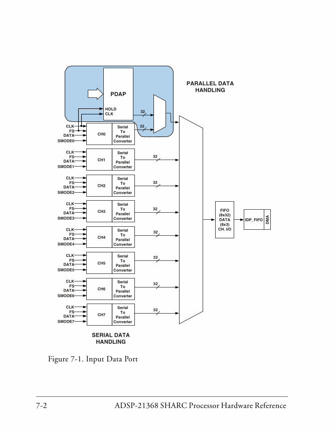
7-2 ADSP-21368 SHARC Processor Hardware Reference
Figure 7-1. Input Data Port
CH7
SerialTo
ParallelConverter
CLKFS
DATASMODE7
PDAP
FIFO(8x32)DATA(8x3)
CH. I/O
32
32
CH0
SerialTo
ParallelConverter
CLKFS
DATASMODE0
32
32
32
32
32
32
32
CH6
SerialTo
ParallelConverter
CLKFS
DATASMODE6
CH5
SerialTo
ParallelConverter
CLKFS
DATASMODE5
CH4
SerialTo
ParallelConverter
CLKFS
DATASMODE4
CH3
SerialTo
ParallelConverter
CLKFS
DATASMODE3
CH2
SerialTo
ParallelConverter
CLKFS
DATASMODE2
CH1
SerialTo
ParallelConverter
CLKFS
DATASMODE1
CLKHOLD
PARALLEL DATAHANDLING
SERIAL DATAHANDLING
IDP_FIFO
DM
A
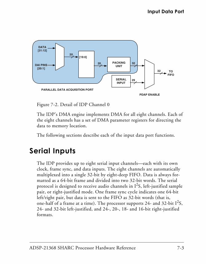
ADSP-21368 SHARC Processor Hardware Reference 7-3
Input Data Port
The IDP’s DMA engine implements DMA for all eight channels. Each of the eight channels has a set of DMA parameter registers for directing the data to memory location.
The following sections describe each of the input data port functions.
Serial InputsThe IDP provides up to eight serial input channels—each with its own clock, frame sync, and data inputs. The eight channels are automatically multiplexed into a single 32-bit by eight-deep FIFO. Data is always for-matted as a 64-bit frame and divided into two 32-bit words. The serial protocol is designed to receive audio channels in I2S, left-justified sample pair, or right-justified mode. One frame sync cycle indicates one 64-bit left/right pair, but data is sent to the FIFO as 32-bit words (that is, one-half of a frame at a time). The processor supports 24- and 32-bit I2S, 24- and 32-bit left-justified, and 24-, 20-, 18- and 16-bit right-justified formats.
Figure 7-2. Detail of IDP Channel 0
PDAP ENABLE
DAI PINS[20:1]
DATA[31:12]
[19:0]20
20 PACKINGUNIT
SERIALINPUT
29
32
32 TOFIFO
PARALLEL DATA ACQUISITION PORT

Serial Inputs
7-4 ADSP-21368 SHARC Processor Hardware Reference
An audio signal that is normally 24 bits wide is contained within the 32-bit word. Four more bits are available for status and formatting data (compliant with the IEC 90958, S/PDIF, and AES3 standards). An addi-tional bit identifies the left/right one-half of the frame. If the data is not in IEC standard format, the serial data can be any data word up to 28 bits wide. Regardless of mode, bit 3 always specifies whether the data is received in the first half (left channel) or the second half (right channel) of the same frame, as shown in Figure 7-3. The remaining three bits are used to encode one of the eight channels being passed through the FIFO to the core. The FIFO output may feed eight DMA channels, where the appro-priate DMA channel (corresponding to the channel number) is selected automatically.
Note that each input channel has its own clock and frame sync input, so unused IDP channels do not produce data and therefore have no impact on FIFO throughput. The clock and frame sync of any unused input should be assigned to low to avoid unintentional acquisition. The input data port supports a maximum clock speed of 41.6 MHz.
The framing format is selected by using the IDP_SMODEx bits (three bits per channel) in the IDP_CTL0 register. The bits (31–8) of the IDP_CTL0 register control the input format modes for each of the eight channels. The eight groups of three bits indicate the mode of the serial input for each of the eight IDP channels, as shown in Table 7-1.
Figure 7-4 through Figure 7-9 show the FIFO data packing for the differ-ent serial modes.
Figure 7-3. Word Format
31 8 7 4 3 2 0
AUDIO DATA (24 BITS) AUDIO STREAMSTATUS L/R
IDPCHNL

ADSP-21368 SHARC Processor Hardware Reference 7-5
Input Data Port
Table 7-1. Serial Modes
Bit Field ValuesIDP_SMODEx
Mode
000 Left-justified sample pair
001 I2S
010 Left-justified 32 bits. This is a single data and not a left/right channel pair. It can be read as 32-bit data.
011 I2S-32 bit. This is a single data and not a left/right channel pair. It can be read as 32-bit data.
100 Right-justified sample pair 24 bits
101 Right-justified sample pair 20 bits
110 Right-justified sample pair 18 bits
111 Right-justified sample pair 16 bits
Figure 7-4. FIFO Data Packing for I2S and Left-Justified
Figure 7-5. FIFO Data Packing for Right-Justified
ChannelEncodingBits (2–0)
L/R Encoding
Block Status
Channel
User Data
Validity
24-BitAudioData (31–8)
34567
Status
ChannelEncodingBits (2–0)
L/R Encoding
Spare Bits (7–4) 24-BitAudioData (31–8)
3Set to LOW

Serial Inputs
7-6 ADSP-21368 SHARC Processor Hardware Reference
The polarity of left/right encoding is independent of the serial mode frame sync polarity selected in IDP_SMODE for that channel (Table 7-1). Note that I2S mode uses a low frame sync (left/right) signal to dictate the first (left) channel, and left-justified sample pair mode uses a HIGH frame sync (left/right) signal to dictate the first (left) channel of each frame. In either mode, the left channel has bit 3 set (= 1) and the right channel has bit 3 cleared (= 0).
Figure 7-6. FIFO Data Packing for Right-Justified (20-Bit Data)
Figure 7-7. FIFO Data Packing for Right-Justified (18-Bit Data)
Figure 7-8. FIFO Data Packing for Right-Justified (16-Bit Data)
Figure 7-9. FIFO Data Packing for I2S and Left-Justified (32-Bit Data)
ChannelEncodingBits (2–0)
L/R Encoding
Spare Bits (11–4) 20-BitAudioData (31–12)
3Set to LOW
ChannelEncodingBits (2–0)
L/R Encoding
Spare Bits (13–4) 18-BitAudioData (31–14)
3Set to LOW
ChannelEncodingBits (2–0)
L/R Encoding
Spare Bits (15–4) 16-BitAudioData (31–16)
3Set to LOW
16-Bit Audio Data (31–0)

ADSP-21368 SHARC Processor Hardware Reference 7-7
Input Data Port
Figure 7-10 shows the relationship between frame sync, serial clock, and left-justified sample pair data.
Figure 7-11 shows the relationship between frame sync, serial clock, and I2S data.
Figure 7-10. Timing in Left-justified Sample Pair Mode
Figure 7-11. Timing in I2S Mode
SERIAL CLOCKIDPx_CLK_I
FRAME SYNC (L/R)IDPx_FS_I
LEFT-JUSTIFIEDSAMPLE PAIRSERIAL DATA
IDPx_DAT_I
MSBn
F RAME [n] FRAME [n]
LSBn MSBn
FRAME [n-1]
LSBn-1
RIGHT LEFT RIGHT
0 63 62 3261 31
SERIAL CLOCKIDPx_CLK_I
FRAME SYNC (L/R)IDPx_F S_I
I2S SERIAL DATAIDPx_DAT_I MSBn
F RAME [n] FRAME [n]
LSBn MSBn
FRAME [n-1]
LSBn-1
0 63 62 32 3133
RIGHT LEFT RIGHT

Parallel Data Acquisition Port (PDAP)
7-8 ADSP-21368 SHARC Processor Hardware Reference
Parallel Data Acquisition Port (PDAP)The input to channel 0 of the IDP is multiplexed, and may be used either in the serial mode, described in “Serial Inputs” on page 7-3, or in a direct parallel input mode. Serial or parallel input is selected by setting IDP_PDAP_EN bit 31 in the IDP_PP_CTL register. When used in parallel mode, the clock input for channel 0 is used to latch parallel subwords. Multiple latched parallel subword samples may be packed into 32-bit words for efficiency. The frame sync input is used to hold off latching of the next sample (that is, ignore the clock edges). The data then flows through the FIFO and is transferred by a dedicated DMA channel into the core’s memory as with any IDP channel. As shown in Figure 7-12, the PDAP can accept input words up to 20 bits wide, or can accept input words that are packed as densely as 4 input words up to 8 bits wide.
The IDP_PP_CTL register also provides a reset bit that zeros any data that is waiting in the packing unit to be latched into the FIFO. When asserted, the IDP_PDAP_RESET bit (bit 30 in the IDP_PP_CTL register) causes the reset circuit to strobe, then automatically clear itself. Therefore, this bit always returns a value of zero when read. The IDP_PORT_SELECT bit
Figure 7-12. Parallel Data Acquisition Port (PDAP) Functions
DATA[31:12]
DAI PINS[20:1]
IDP_PORT_SELECT(IDP_PP_CTL[26])
1
[19:0]
MASK
20
IDP_Pxx_MASK(IDP_PP_CTL[19:0])
20 PACKINGUNIT
IDP_PP_PACKING(IDP_PP_CTL[28:27])
2
SERIALINPUT
29
32
IDP_PP_EN(IDP_PP_CTL[31])
32 TOFIFO
20 1

ADSP-21368 SHARC Processor Hardware Reference 7-9
Input Data Port
(bit 26 in the IDP_PP_CTL register) selects between the two sets of pins that may be used as the parallel input port. When IDP_PORT_SELECT is set (= 1), the data bits are read from DATA31–12 and the control signals come from DATA11-8. When IDP_PORT_SELECT is cleared (= 0), the data bits are read from DAI_P20–1. When IDP_PORT_SELECT is set to 1, the PDAP can be operated through data pins alone (data and controls can be completely routed through the DATA pins).
MaskingThe IDP_PP_CTL register provides 20 mask bits that allow the input from any of the 20 pins to be ignored. The mask is specified by setting the IDP_Pxx_PDAPMASK bits (bits 19–0 of the IDP_PP_CTL register) for the 20 parallel input signals. For each of the parallel inputs, a bit is set (= 1) to indicate the bit is unmasked and therefore its data can be passed on to read, or a bit is masked (= 0) so its data is not read. After this masking pro-cess, data gets passed along to the packing unit.
Packing UnitThe parallel data acquisition port (PDAP) packing unit receives masked parallel subwords from the 20 parallel input signals and packs them into a 32-bit word. The IDP_PDAP_PACKING bit field (bits 28–27 of the IDP_PP_CTL register), indicates how data is to be packed. Data can be packed in any of four modes. Selection of packing mode is made based on the application.
Packing Mode 11
Mode 11 provides for 20 bits coming into the packing unit and 32 bits going out to the FIFO in a single cycle. On every clock edge, 20 bits of data are moved and placed in a 32-bit register, left-aligned. That is, bit 19 maps to bit 31. The lower bits, 11–0, are always set to zero, as shown in Figure 7-13.

Parallel Data Acquisition Port (PDAP)
7-10 ADSP-21368 SHARC Processor Hardware Reference
This mode sends one 32-bit word to FIFO for each input clock cycle—the DMA transfer rate matches the PDAP input clock rate.
Packing Mode 10
On the first clock edge (cycle A), the packing unit latches parallel data up to 16 bits wide (bits 19–4 of the parallel input) and places it in bits 15–0 (the lower half of the word), then waits for the second clock edge (cycle B). On the second clock edge (cycle B), the packing unit takes the same set of inputs and places the word into bits 31–16 (the upper half of the word).
This mode sends one packed 32-bit word to FIFO for every two input clock cycles—the DMA transfer rate is one-half the PDAP input clock rate.
Figure 7-13. Packing Modes in PDAP
31 24 23 16 15 7 0
31 21 20 10 9 0
31 16 15 0
MODE 102x16-bit
MODE 01tri-word
MODE 004x8-bit
B A
ABC
ABCD
MODE 111x20-bit
31 12 11 0
A RESERVED
8

ADSP-21368 SHARC Processor Hardware Reference 7-11
Input Data Port
Packing Mode 01
Mode 01 packs three acquired samples together. Since the resulting 32-bit word is not divisible by three, up to 10 bits are acquired on the first clock edge and up to 11 bits are acquired on each of the second and third clock edges:
• On clock edge 1, bits 19–10 are moved to bits 9–0 (10 bits)
• On clock edge 2, bits 19–9 are moved to bits 20–10 (11 bits)
• On clock edge 3, bits 19–9 are moved to bits 31–21 (11 bits)
This mode sends one packed 32-bit word to FIFO for every three input clock cycles—the DMA transfer rate is one-third the PDAP input clock rate.
Packing Mode 00
Mode 00 moves data in four cycles. Each input word can be up to 8 bits wide.
• On clock edge 1, bits 19–12 are moved to bits 7–0
• On clock edge 2, bits 19–12 are moved to bits 15–8
• On clock edge 3, bits 19–12 are moved to bits 23–16
• On clock edge 4, bits 19–12 are moved to bits 31–24
This mode sends one packed 32-bit word to FIFO for every four input clock cycles—the DMA transfer rate is one-quarter the PDAP input clock rate.

Parallel Data Acquisition Port (PDAP)
7-12 ADSP-21368 SHARC Processor Hardware Reference
Clocking Edge SelectionNotice that in all four packing modes described, data is read on a clock edge, but the specific edge used (rising or falling) is not indicated. Clock edge selection is configured using the IDP_PDAP_CLKEDGE bit (bit 29 of the IDP_PP_CTL register). Setting this bit (= 1) causes the data to latch on the falling edge. Clearing this bit (= 0) causes data to latch on the rising edge (default).
Hold InputA synchronous clock enable signal can be passed from any DAI pin to the PDAP packing unit. This signal is called PDAP_HOLD.
The PDAP_HOLD signal is actually the same physical internal signal as the frame sync for IDP channel 0. Its functionality is determined by the PDAP enable bit (IDP_PDAP_EN).
When the PDAP_HOLD signal is HIGH, all latching clock edges are ignored and no new data is read from the input pins. The packing unit operates as normal, but it pauses and waits for the PDAP_HOLD signal to be deasserted and waits for the correct number of distinct input samples before passing the packed data to the FIFO.
Figure 7-14 shows the affect of the hold input (B) for four 8-bit words in packing mode 00, and Figure 7-15 shows the affect of the hold input (B) for two 16-bit words in packing mode 10.
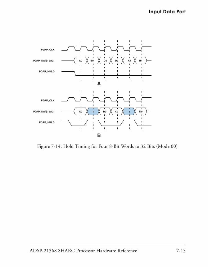
ADSP-21368 SHARC Processor Hardware Reference 7-13
Input Data Port
Figure 7-14. Hold Timing for Four 8-Bit Words to 32 Bits (Mode 00)
PDAP_CLK
PDAP_DAT[19:12]
PDAP_HOLD
B0A0 C0 D0 A1 B1
PDAP_CLK
PDAP_DAT[19:12]
PDAP_HOLD
B0A0 C0 D0
B
A

Parallel Data Acquisition Port (PDAP)
7-14 ADSP-21368 SHARC Processor Hardware Reference
As shown in Figure 7-15, PDAP_DATA and PDAP_HOLD are driven by the inactive edges of the clock (falling edge in the above figures) and these sig-nals are sampled by the active edge of the clock (rising edge in the above figures).
PDAP StrobeWhenever the PDAP packing unit receives the number of subwords corre-sponding to its select mode, it asserts the PDAP output strobe signal. This signal can be routed through the SRU using the MISC unit to any of the DAI pins. See “DAI/SRU1 Connection Groups” on page 4-18 for more information.
Figure 7-15. Hold Timing for Two 16-Bit Words to 32 Bits (Mode 10)
PDAP_CLK
PDAP_DAT[19:4]
PDAP_HOLD
BA A B A B
PDAP_CLK
PDAP_DAT[19:4]
PDAP_HOLD
BA A B
B
A

ADSP-21368 SHARC Processor Hardware Reference 7-15
Input Data Port
FIFO Control and StatusSeveral bits can be used to control and monitor FIFO operations:
• IDP Enable. The IDP_ENABLE bit (bit 7 of the IDP_CTL0 register) enables the IDP. This is a global control bit. This bit and the corre-sponding IDP channel enable bit (IDP_ENx) in the IDP_CTL1 register must be set for data from a channel to get into the FIFO.
• IDP Buffer Hang Disable. The IDP_BHD bit (bit 4 in the IDP_CTL0 register) determines whether or not the core hangs on reads when the FIFO is empty.
• Number of Samples in FIFO. The IDP_FIFOSZ bits (bits 31–28 in the DAI_STAT register) monitor the number of valid data words in the FIFO.
• FIFO Overflow Status. The SRU_OVFx bits in the DAI_STAT register monitor the overflow error conditions in the FIFO for each of the channels.
• FIFO Overflow Clear. The IDP_CLROVR bit (bit 6 of the IDP_CTL0 register) clears an indicated FIFO overflow error.
To enable the IDP, two separate bits in two different registers must be set. The first is the IDP_ENABLE bit in the IDP_CTL0 register and the second is the specific channel enable bit which is located in the IDP_CTL1 register. When these bits are set (= 1), the IDP is enabled. When these bits are cleared (= 0), the IDP is disabled, and data cannot come to the IDP_FIFO register from the IDP channels. When the IDP_ENABLE bit transitions from 1 to 0, all data in the IDP FIFO is cleared. Writing a 1 to bit 31 of the IDP_CTL1 register also clears the FIFO. This is a write-only bit and always returns a zero on reads.
The IDP_BHD bit is used for buffer hang disable control. When there is no data in the FIFO, reading the IDP_FIFO register causes the core to hang. This condition continues until the FIFO contains valid data. Setting the

FIFO to Memory Data Transfer
7-16 ADSP-21368 SHARC Processor Hardware Reference
IDP_BHD bit (= 1) prevents the core from hanging on reads from an empty IDP_FIFO register. Clearing this bit (= 0) causes the core to hang under the conditions described previously.
The IDP_FIFOSZ bits track the number of words in the FIFO. This 4-bit field identifies the number of valid data samples in the IDP FIFO.
The SRU_OVF bits (bits 8–15) in the DAI_STAT register provide IDP FIFO overflow status information for each of the channels. These bits are set (= 1), whenever an overflow occurs. When these bits are cleared (= 0), it indicates there is no overflow condition. These read-only bits are W1C bits, which do not automatically reset to 0 when an overflow condition changes to a no-overflow condition. These bits must be reset manually, using the IDP_CLROVR bit in the IDP_CTL0 register. Writing one to this bit clears the overflow conditions for the channels in the DAI_STAT register. Since IDP_CLROVR is a write-only bit, it always returns low when read.
FIFO to Memory Data TransferThe data from each of the eight IDP channels is inserted into an eight-reg-ister deep FIFO, which can only be transferred to the core’s memory space sequentially. Data is moved into the FIFO as soon as it is fully received. When more than one channel has data ready, the channels access the FIFO with fixed priority, from a low to high channel number (that is, channel 0 is the highest priority and channel 7 is the lowest priority).
One of two methods can be used to move data from the IDP FIFO to internal memory:
• The core can remove data from the FIFO manually by reading the memory-mapped register, IDP_FIFO. The output of the FIFO is held in the (read-only) IDP_FIFO register. When this register is read, the corresponding element is removed from the IDP FIFO, and the next element is moved into the IDP_FIFO register.

ADSP-21368 SHARC Processor Hardware Reference 7-17
Input Data Port
A mechanism is provided to generate an interrupt when more than a specified number of words are in the FIFO. This interrupt signals the core to read the IDP_FIFO register.
This method of moving data from the IDP FIFO is described in the next section, “IDP Transfers Using the Core”.
• Eight dedicated DMA channels can sort and transfer the data into one buffer per source channel. When the memory buffer is full, the DMA channel raises an interrupt in the DAI interrupt controller.
This method of moving data from the IDP FIFO is described in “IDP Transfers Using DMA” on page 7-20.
IDP Transfers Using the CoreThe output of the FIFO can be directly fetched by reading from the IDP_FIFO register. The IDP_FIFO register is used only to read and remove the top sample from the FIFO, which is eight locations deep.
As data is read from the IDP_FIFO register, it is removed from the FIFO and new data is copied into the register. The contents of the IDP_NSET bits (bits 3–0 in the IDP_CTL0 register) represent a threshold number of entries (N) in the FIFO. When the FIFO fills to a point where it has more than N words (data in FIFO exceeds the value set in the IDP_NSET bit field), a DAI interrupt is generated. This DAI interrupt corresponds to the IDP_FIFO_GTN_INT bit, the eighth-level interrupt in the DAI_IRPTL_L or DAI_IRPTL_H registers. The core uses this interrupt to detect when data needs to be read.

FIFO to Memory Data Transfer
7-18 ADSP-21368 SHARC Processor Hardware Reference
Starting an Interrupt-Driven Transfer
To start an interrupt-driven transfer:
1. Clear and halt FIFO by setting (= 1) and clearing (= 0) the IDP_ENABLE bit (bit 7 in the IDP_CTL0 register).
2. Set the required values for:
• IDP_SMODEx bits in the IDP_CTL0 register to specify the frame sync format for the serial inputs (left-justified sample pair, right-justified sample pair, or I2S mode).
• IDP_Pxx_PDAPMASK bits in the IDP_PP_CTL register to specify the input mask, if the PDAP is used.
• IDP_PORT_SELECT bits in the IDP_PP_CTL register to specify input from the DAI pins, if the PDAP is used.
• IDP_PDAP_CLKEDGE bit (bit 29) in the IDP_PP_CTL register to specify if data is latched on the rising or falling clock edge, if the PDAP is used.
3. Keep the clock and frame sync inputs of all serial inputs and/or the PDAP connected to low. Use the SRU_CLK2, SRU_CLK3, SRU_FS2, and SRU_FS3 registers to specify these inputs. See “Group A Con-nections—Clock Signals” on page 4-19 and “Group C Connections—Frame Sync Signals” on page 4-31.
4. Connect all of the inputs to the IDP by writing to the SRU_DAT4, SRU_DAT5, SRU_FS2, SRU_FS3, SRU_CLK2, and SRU_CLK3 registers. Connect the clock and frame sync of any unused ports to low.
5. Set the desired value for the N_SET variable (the IDP_NSET bits, 3–0, in the IDP_CTL0 register).

ADSP-21368 SHARC Processor Hardware Reference 7-19
Input Data Port
6. Set the IDP_FIFO_GTN_INT bit (bit 8 of the DAI_IRPTL_RE register) to HIGH and set the corresponding bit in the DAI_IRPTL_FE register to low to unmask the interrupt. Set bit 8 of the DAI_IRPTL_PRI reg-ister (IDP_FIFO_GTN_INT) as needed to generate a high priority or low priority core interrupt when the number of words in the FIFO is greater than the value of N set.
7. Enable the PDAP by setting the IDP_PDAP_EN bit (bit 31 in the IDP_PP_CTL register), if required.
8. Enable the IDP by setting the IDP_ENABLE bit (bit 7 in the IDP_CTL0 register) and the IDP_ENx bits in the IDP_CTL1 register.
Do not set the IDP_DMA_EN bit (bit 5 of the IDP_CTL0 register) as this enables DMA transfers.
Core Transfer Notes
The following items provide general information about interrupt-driven transfers.
• The three LSBs of FIFO data are the encoded channel number. These are transferred “as is” for this mode. These bits can be used by software to decode the source of data.
• The number of data samples in the FIFO at any time is reflected in the IDP_FIFOSZ bit field (bits 31–28 in the DAI_STAT register), which tracks the number of samples in FIFO.
When using the interrupt scheme, the IDP_NSET bits (bits 3–0 of the IDP_CTL0 register) can be set to N, so N + 1 data can be read from the FIFO in the interrupt service routine (ISR).
• If the IDP_BHD bit (bit 4 in the IDP_CTL0 register) is not set, attempts to read more data than is available in the FIFO results in a core hang.

FIFO to Memory Data Transfer
7-20 ADSP-21368 SHARC Processor Hardware Reference
• When the data transfer to the core is 32 bits, as in the case of PDAP data or I2S and left-justified modes with 32 bits, there is no channel information in the data. Therefore, PDAP or I2S and left-justified 32 bit modes can not be used with other channels in the core/interrupt-driven mode.
IDP Transfers Using DMAThe ADSP-21367/8/9 and ADSP-2137x processors support two types of DMA transfers, simple and ping-pong.
Simple DMA
This DMA access is enabled when the IDP_DMA_EN bit (bit 5 of the IDP_CTL0 register) is set (= 1) and the IDP_DMA_ENx bits in the IDP_CTLl register are set to select a particular channel.
The DMA is performed according to the parameters set in the various DMA registers and IDP control registers. The DMA transfer is completed when the count register (IDP_DMA_Cx) reaches zero. The IDP_DMA_EN bit and IDP_DMA_ENx bits must be reset before starting another DMA. An interrupt is generated at the end of DMA transfer.
Starting a Simple DMA Transfer
To start a DMA transfer from the FIFO to memory:
1. Clear and halt the FIFO by setting (= 1) and then clearing (= 0) the IDP_ENABLE bit (bit 7 in the IDP_CTL0 register).
2. While the IDP_DMA_EN and IDP_ENABLE bits are low, set the values for the DMA parameter registers that correspond to channels 7–0. If some channels are not going to be used, then the corresponding parameter registers can be left in their default states:

ADSP-21368 SHARC Processor Hardware Reference 7-21
Input Data Port
• Index registers (IDP_DMA_Ix)
• Modifier registers (IDP_DMA_Mx)
• Counter registers (IDP_DMA_Cx)
For each of these registers, x is 0 to 7. Refer to “DMA Channel Parameter Registers” on page 7-27.
3. Keep the clock and the frame sync input of the serial inputs and/or the PDAP connected to low, by setting proper values in the SRU_CLK2, SRU_CLK3, SRU_FS2, and SRU_FS3 registers.
4. Set required values for:
• IDP_SMODEx bits in the IDP_CTL0 register to specify the frame sync format for the serial inputs (left-justified sample pair, right-justified sample pair, or I2S modes).
• IDP_Pxx_PDAPMASK bits in the IDP_PP_CTL register to specify the input mask, if the PDAP is used.
• IDP_PORT_SELECT bits in the IDP_PP_CTL register to specify input from the DAI pins or the IDP, if the PDAP is used.
• IDP_PDAP_CLKEDGE bit (bit 29) in the IDP_PP_CTL register to specify if data is latched on the rising or falling clock edge, if the PDAP is used.
5. Connect all of the inputs to the IDP by writing to the SRU_DAT4, SRU_DAT5, SRU_FS2, SRU_FS3, SRU_CLK2, and SRU_CLK3 registers. Keep the clock and frame sync of the ports connected to low when data transfer is not intended.

FIFO to Memory Data Transfer
7-22 ADSP-21368 SHARC Processor Hardware Reference
6. Enable DMA, IDP, and PDAP (if required) by setting each of the following bits = 1:
• IDP_DMA_EN bit (bit 5 of the IDP_CTL0 register)
• IDP_DMA_ENx bits in IDP_CTL1 register to enable the DMA of the selected channel
• IDP_PDAP_EN bit (bit 31 in IDP_PP_CTL register)
• IDP_ENx of IDP_CTL1 to enable the selected channel
• IDP_ENABLE bit (bit 7 in the IDP_CTL0 register)
A DAI interrupt is generated at the end of each DMA.
7. After the DMA completes, connect the clock and frame sync sig-nals to 0.
Ping-Pong DMA
This mode gets activated when the IDP_DMA_EN bit of the IDP_CTL0 register and the IDP_PINGx bit in the IDP_CTL1 register are set for a particular channel.
In ping-pong DMA, the parameters have two memory index values (index A and index B), one count value and one modifier value. The DMA starts the transfer with the memory indexed by A. When the transfer is com-pleted as per the value in the count register, the DMA restarts with the memory location indexed by B. The DMA restarts with index A after the transfer to memory with index B is completed as per the count value. This repeats until the DMA is stopped by resetting the IDP_DMA_EN or IDP_PINGx bits.

ADSP-21368 SHARC Processor Hardware Reference 7-23
Input Data Port
Starting Ping-Pong DMA Transfers
To start a ping-pong DMA transfer from the FIFO to memory:
1. Clear and halt the FIFO by setting (= 1) and then clearing (= 0) the IDP_ENABLE bit (bit 7 in the IDP_CTL0 register).
2. While the IDP_DMA_EN and IDP_ENABLE bits are low, set the values for the following DMA parameter registers that correspond to channels 7–0. If some channels are not going to be used, then the corresponding parameter registers can be left in their default states:
• First index registers IDP_DMA_AIx
• Second index registers IDP_DMA_BIx
• Modifier register IDP_DMA_Mx
• Counter register IDP_DMA_PCx. For each of these registers x is 0–7 which corresponds to channels 0 to 7. See “IDP Ping-Pong Count Registers (IDP_DMA_PCx)” on page A-73.
3. Keep the clock and the frame sync input of the serial inputs and/or the PDAP connected to low, by setting proper values in the SRU_CLK2 and SRU_CLK3 as well as the SRU_FS2 and SRU_FS3 regis-ters. For more information, see “DAI/SRU1 Connection Groups” on page 4-18.
4. Set the required values for:
• IDP_SMODEx bits in the IDP_CTL0 register to specify the frame sync format for the serial inputs (I 2S, left-justified sample pair, or right-justified sample pair modes).

FIFO to Memory Data Transfer
7-24 ADSP-21368 SHARC Processor Hardware Reference
• IDP_Pxx_PDAPMASK bits in the IDP_PP_CTL register to specify the input mask, if the PDAP is used. For more information, see “Parallel Data Acquisition Port Control Register (IDP_PP_CTL)” on page A-74.
• IDP_PORT_SELECT bits in the IDP_PP_CTL register to specify input from the DAI pins or the data pins, if the PDAP is used.
• IDP_PDAP_CLKEDGE bit (bit 29) in the IDP_PP_CTL register to specify if data is latched on the rising or falling clock edge, if the PDAP is used.
5. Connect all of the inputs to the IDP by writing to the SRU_DAT4 and SRU_DAT5, SRU_FS2 and SRU_FS3, SRU_CLK2 and SRU_CLK3 regis-ters. Keep the clock and frame sync of the ports connected to low when data transfer is not intended.
6. Enable DMA, IDP, and PDAP (if required) by setting each of the following bits = 1:
• IDP_DMA_EN bit (bit 5 of the IDP_CTL0 register)
• IDP_PINGx bit in IDP_CTL1 register to enable the ping-pong DMA of the selected channel
• IDP_PDAP_EN bit (bit 31 in IDP_PP_CTL register)
• IDP_ENx of IDP_CTL1 to enable the selected channel
• IDP_ENABLE bit (bit 7 in the IDP_CTL0 register)
7. After the DMA completes, connect the clock and frame sync sig-nals to 0.
An interrupt is generated after every ping and pong DMA transfer (when the count = 0).

ADSP-21368 SHARC Processor Hardware Reference 7-25
Input Data Port
DMA Transfer Notes
The following items provide general information about DMA transfers.
• A DMA can be interrupted by changing the IDP_DMA_EN bit in the IDP_CTL0 register. None of the other control settings (except for the IDP_ENABLE bit) should be changed. Clearing the IDP_DMA_EN bit (= 0) does not affect the data in the FIFO, it only stops DMA transfers. If the IDP remains enabled, an interrupted DMA can be resumed by setting the IDP_DMA_EN bit again. But resetting the IDP_ENABLE bit flushes the data in the FIFO. If the bit is set again, FIFO starts accepting new data.
• Using DMA transfers overrides the mechanism that is used for interrupt-driven manual reads from the FIFO. When the IDP_DMA_EN bit and at least one IDP_DMA_ENx bit in the IDP_CTL1 register are set, the eighth interrupt in the DAI_IRPTL_L or DAI_IRPTL_H registers (IDP_FIFO_GTN_INT) is not generated. This interrupt detects the condition that the number of data available in FIFO is more than the number set in the IDP_NSET bits (bits 3–0 of the IDP_CTL0 register).
• At the end of the DMA transfer for individual channels, interrupts are generated. These interrupts are generated after the last DMA data from a particular channel has been transferred to memory. These interrupts are mapped to the IDP_DMA7_INT bit (bit 17), and to the IDP_DMA0_INT bit (bit 10) in the DAI_IRPTL_L or DAI_IRPTL_H registers and they generate interrupts when they are set (= 1). These bits are ORed and reflected in high-level interrupts sent to the core.
• If the combined data rate from the channels is more than the DMA can service, a FIFO overflow occurs. This condition is reflected for each channel by the individual overflow bits (SRU_OVF) in the DAI_STAT register. These are W1C bits that must be cleared by writing to the IDP_CLROVR bit (bit 6 of the IDP_CTL0 register).

FIFO to Memory Data Transfer
7-26 ADSP-21368 SHARC Processor Hardware Reference
When an overflow occurs, incoming data from IDP channels is not accepted into the FIFO, and data values are lost. New data is only accepted once space is again created in the FIFO.
• For serial input channels, data is received in an alternating fashion from left and right channels. Data is not pushed into the FIFO as a full left/right frame. Rather, data is transferred as alternating left/right words as it is received. For the PDAP and 32-bit (non-audio) serial input, data is transferred as packed 32-bit words.
• The state of all eight DMA channels is reflected in the IDP_DMAx_STAT bits (bits 24–17 of DAI_STAT register). These bits are set once the IDP_DMA_EN bit and IDP_DMA_ENx bits are set, and remain set until the last data from that channel is transferred. Even if IDP_DMA_EN bit and IDP_DMA_ENx bits remain set, this bit clears once the required number of data transfers takes place. For more information, see “DAI Pin Buffer Status Register (DAI_PIN_STAT)” on page A-112.
Note that when a DMA channel is not used (that is, parameter reg-isters are at their default values) that DMA channel’s corresponding IDP_DMAx_STAT bit is set (= 1).
• The three LSBs of data from the serial inputs are channel encoding bits. Since the data is placed into a separate buffer for each channel, these bits are not required and are set to low when transferring data to internal memory through the DMA. Bit 3 still contains the left/right status information. In the case of PDAP data or 32-bit I2S and left-justified modes, these three bits are part of the 32-bit data.
• An interrupt is generated at the end of a DMA, which is cleared by reading the DAI_IRPTL_H or DAI_IRPTL_L registers.
• A read of the DAI_IRPTL_H_SH register provides the same data as a read of the DAI_IRPTL_H register. Likewise, a read of the DAI_IRPTL_L_SH register provides the same data as a read of the

ADSP-21368 SHARC Processor Hardware Reference 7-27
Input Data Port
DAI_IRPTL_L register. Reading these DAI shadow registers (DAI_IRPTL_H_SH and DAI_IRPTL_L_SH) does not destroy the con-tents of the DAI_IRPTL_H and DAI_IRPTL_L registers.
• The IDP can run both simple and ping-pong DMAs in different channels. When running simple DMA, initialize the corresponding IDP_DMA_Ix, IDP_DMA_Mx, and IDP_DMA_Mx registers. When running ping-pong DMA, initialize the corresponding IDP_DMA_AIx, IDP_DMA_BIx, IDP_DMA_Mx, and IDP_DMA_PCx registers.
• A new feature of dropping DMA requests from the FIFO has been added. If one channel has finished its DMA, but the IDP_DMA_EN bit is still high, any data corresponding to that channel is skipped by the DMA controller. This feature is provided to avoid stalling the DMA of other channels, which are still in an active DMA state. To avoid this data loss, programs can toggle IDP_DMA_EN low.
• Disabling IDP DMA by resetting the IDP_DMA_EN bit requires 1 HCLK cycle. Disabling an individual channel DMA by resetting the IDP_DMA_ENx bits requires 2 HCLK cycles.
DMA Channel Parameter RegistersThe eight DMA channels each have two sets of registers for simple and ping-pong DMA. For simple DMA, an I-register (index pointer, 19 bits), an M-register (modifier/stride, 6 bits), and a C-register (count, 16 bits) are used. For ping-pong DMA, A and B index registers (AI/BI register pointer, 19 bits) and a PC register (DMA count, 16 bits) are used, along with the M-register.

FIFO to Memory Data Transfer
7-28 ADSP-21368 SHARC Processor Hardware Reference
The IDP DMA parameter registers have these functions:
• Internal index registers (IDP_DMA_Ix, IDP_DMA_AIx, IDP_DMA_BIx). Index registers provide an internal memory address, acting as a pointer to the next internal memory location where data is to be written.
• Internal modify registers (IDP_DMA_Mx). Modify registers provide the signed increment by which the DMA controller post-modifies the corresponding internal memory index register after each DMA write.
• Count registers (IDP_DMA_Cx, IDP_DMA_PCx). Count registers indi-cate the number of words remaining to be transferred to internal memory on the corresponding DMA channel.
For a descriptions of these registers see “Input Data Port DMA Control Registers” on page A-70 and “Input Data Port Ping-Pong DMA Regis-ters” on page A-72.
IDP (DAI) Interrupt Service Routines for DMAsThe IDP can trigger either the high priority DAI core interrupt reflected in the DAI_IRPTL_H register or the low priority DAI core interrupt reflected in the DAI_IRPTL_L register. The ISR must read the correspond-ing DAI_IRPTL_H or DAI_IRPTL_L register to find all the interrupts currently latched. The DAI_IRPTL_H register reflects the high priority inter-rupts and the DAI_IRPTL_L register reflects the low priority interrupts. When these registers are read, it clears the latched interrupt bits. This is a destructive read.

ADSP-21368 SHARC Processor Hardware Reference 7-29
Input Data Port
The following steps describe how an IDP ISR is handled.
1. When the DMA for a channel completes, an interrupt is generated and program control jumps to the ISR.
2. The program clears the IDP_DMA_EN bit in the IDP_CTL0 register (= 0).
3. The program should read the DAI_IRPTL_L or DAI_IRPTL_H registers to determine which DMA channels have completed. Programs may read these register’s shadow registers (DAI_IRPTL_L_SH and DAI_IRPTL_H_SH) without clearing the contents of the primary registers.
To ensure that the DMA of a particular IDP channel is complete, (all data is transferred into internal memory) wait until the IDP_DMAx_STAT bit of that channel becomes zero in the DAI_STAT register. This is required if a high priority DMA (for example a SPORT DMA) is occurring at the same time as the IDP DMA.
As each DMA channel completes, a corresponding bit in either the DAI_IRPTL_L or DAI_IRPTL_H registers for each DMA channel is set (IDP_DMAx_INT). Refer to “DAI Interrupt Controller Registers” on page A-112 for more information on the DAI_IRPTL_L or DAI_IRPTL_H registers.
4. Reprogram the DMA registers for finished DMA channels.
More than one DMA channel may have completed during this time period. For each channel, a bit is latched in the DAI_IRPTL_L or DAI_IRPTL_H registers. Ensure that the DMA registers are repro-grammed. If any of the channels are not used, then its clock and frame sync must be held low.
FIFO to Memory Data Transfer
7-30 ADSP-21368 SHARC Processor Hardware Reference
5. Read the DAI_IRPTL_L or DAI_IRPTL_H registers to see if more inter-rupts have been generated.
• If the value(s) are not zero, repeat step 4.
• If the value(s) are zero, continue to step 6.
6. Re-enable the IDP_DMA_EN bit in the IDP_CTL0 register (set to 1).
7. Exit the ISR.
If a zero is read in step 5 (no more interrupts are latched), then all of the interrupts needed for that ISR have been serviced. If another DMA com-pletes after step 5 (that is, during steps 6 or 7), as soon as the ISR completes, the ISR is called again because the OR of the latched bits will be nonzero again. DMAs in process run to completion.
If step 5 is not performed, and a DMA channel expires during step 4, then when IDP DMA is re-enabled (step 6), the completed DMA will not have been reprogrammed and its buffer will overrun.
FIFO OverflowIf the data out of the FIFO (either through DMA or core reads) is not suf-ficient to transfer at the combined data rate of all the channels, then a FIFO overflow can occur. When this happens, new data is not accepted. Additionally, data coming from the serial input channels (except for 32-bit I2S and left-justified modes) are not accepted in pairs, so that alter-nate data from a channel is always from left and right channels. If overflow occurs, then sticky bits in the DAI_STAT register are set and an interrupt is generated. Data is accepted again when space has been created in the FIFO.

ADSP-21368 SHARC Processor Hardware Reference 7-31
Input Data Port
Input Data Port Programming ExampleListing 7-1 shows a data transfer using an interrupt service routine (ISR). The transfer takes place through the digital applications interface (DAI). This code implements the algorithm outlined in “FIFO to Memory Data Transfer” on page 7-16.
Listing 7-1. Interrupt-Driven Data Transfer
/* Using Interrupt-Driven Transfers from the IDP FIFO */
#define IDP_ENABLE (8) /* IDP_ENABLE = IDP_CTL0[7] */
#define IDP_CTL0 (0x24B0) /* Memory-mapped register */
#define IDP_FIFO_GTN_INT (8) /* Bit 8 in interrupt regs */
#define IDP_FIFO (0x24D0) /* IDP FIFO packing mode */
#define DAI_IRPTL_FE (0x2480) /* Falling edge int latch */
#define DAI_IRPTL_RE (0x2481) /* Rising edge int latch */
#define DAI_IRPTL_PRI (0x2484) /* Interrupt priority */
.section/dm seg_dmda;
.var OutBuffer[6];
.section/pm seg_pmco;
initIDP:
r0 = dm(IDP_CTL0); /* Reset the IDP */
r0 = BSET r0 BY IDP_ENABLE;
dm(IDP_CTL0) = r0;
r0 = BCLR r0 BY IDP_ENABLE;
r0 = BCLR r0 BY 10; /* Set IDP serial input channel 0 */
r0 = BCLR r0 BY 9; /* to receive in I2S format */
r0 = BCLR r0 BY 8;

Input Data Port Programming Example
7-32 ADSP-21368 SHARC Processor Hardware Reference
dm(IDP_CTL0) = r0;
/*************************************************/
/* Connect the clock, data and frame sync of IDP */
/* channel 0 to DAI pin buffers 10, 11 and 12. */
/*************************************************/
/* Connect IDP0_CLK_I to DAI_PB10_O */
/* (SRU_CLK1[19:15] = 01001) */
/* Connect IDP0_DAT_I to DAI_PB11_O */
/* (SRU_DAT3[11:6] = 001010) */
/* Connect IDP0_FS_I to DAI_PB12_O */
/* (SRU_FS1[19:15] = 01011) */
/******************************************************/
/* Pin buffers 10, 11 and 12 are always being used as */
/* inputs. Tie their enables to LOW (never driven). */
/******************************************************/
/* Connect PBEN10_I to LOW */
/* (SRU_PIN1[29:24] = 111110) */
/* Connect PBEN11_I to LOW */
/* (SRU_PIN2[5:0] = 111110) */
/* Connect PBEN12_I to LOW */
/* (SRU_PIN2 11–6 = 111110) */
/********************************************************/ /* Assign a value to N_SET. An interrupt will be raised */
/* when there are N_SET+1 words in the FIFO. */
/********************************************************/

ADSP-21368 SHARC Processor Hardware Reference 7-33
Input Data Port
r0 = dm(IDP_CTL0); /* N_SET = 6 */
r0 = BSET r0 BY 0;
r0 = BSET r0 BY 1;
r0 = BSET r0 BY 2;
r0 = BCLR r0 BY 3;
dm(IDP_CTL0) = r0;
r0 = dm(DAI_IRPTL_RE); /* Unmask for rising edge */
r0 = BSET r0 BY IDP_FIFO_GTN_INT;
dm(DAI_IRPTL_RE) = r0;
r0 = dm(DAI_IRPTL_FE); /* Mask for falling edge */
r0 = BCLR r0 BY IDP_FIFO_GTN_INT;
dm(DAI_IRPTL_FE) = r0;
r0 = dm(DAI_IRPTL_PRI); /* Map to high priority in core */
r0 = BSET r0 BY IDP_FIFO_GTN_INT;
dm(DAI_IRPTL_PRI) = r0;
r0 = dm(IDP_CTL0); /* Start the IDP */
r0 = BSET r0 BY IDP_ENABLE;
dm(IDP_CTL0) = r0;
initIDP.end:
IDP_ISR:
i0 = OutBuffer;
m0 = 1;
LCNTR = 5, DO RemovedFromFIFO UNTIL LCE;
r0 = dm(IDP_FIFO);
dm(i0,m0) = r0;
RemovedFromFIFO:
RTI;
IDP_ISR.end:

Input Data Port Programming Example
7-34 ADSP-21368 SHARC Processor Hardware Reference

ADSP-21368 SHARC Processor Hardware Reference 8-1
8 PULSE WIDTH MODULATION
Pulse width modulation (PWM) is a technique for controlling analog cir-cuits with a microprocessor’s digital outputs. PWM is employed in a wide variety of applications, ranging from measurement to communications to power control and conversion.
One of the advantages of PWM is that the signal remains digital all the way from the processor to the controlled system; no digital-to-analog con-version is necessary. By maintaining a digital signal throughout a system, noise effects are minimized.
PWM ImplementationThe PWM modules in the ADSP-21367/8/9 and ADSP-2137x SHARC processors are flexible, programmable, PWM waveform generators that produces switching patterns for various purposes related to motor control, electronic valve control, or audio power control. The PWM module is comprised of four identical groups that contain four PWM outputs each, allowing 16 PWM outputs in total. Figure 8-1 shows a single group. The PWM generator can produce either center-aligned or edge-aligned PWM waveforms. In addition, it can generate complementary signals on two outputs in paired mode or independent signals in non-paired mode.
PWM WaveformsThe PWM module can generate waveforms that are either edge-aligned (left-justified) or center-aligned. Each waveform is described in detail in the following sections.

PWM Implementation
8-2 ADSP-21368 SHARC Processor Hardware Reference
Edge-Aligned Mode
In edge-aligned mode, the PWM waveform is left-justified in the period window. A duty value of zero, programmed through the PWMAx registers, produces a PWM waveform with 50% duty cycle. For even values of period, the PWM pulse width is exactly period ÷ 2, whereas for odd values
Figure 8-1. Example PWM Module Block Diagram
PWMCHAPWMCHB
PWMTMPWMCTRL
PWMCONFIGURATION
REGISTERS
PWMDUTY CYCLEREGISTERS
PWMSTAT
PWMDTPWMSEG
PWMTiming
Unit
DeadTime
ControlUnit
GateDriveUnit
PWMSync PulseControl Unit
PWMInterrupt
Control Unit
PWM_AH
PWM_AL
PWM_BH
PWM_BL
CLK SYNC SR RESET
SYNC CLK
RESETB
PWM_SYNC_IRQ
CLK
PWMSEGPHB BUS
OutputControl
Unit
PWMGSTAT
PWMGCTL} GLOBAL
REGISTERS

ADSP-21368 SHARC Processor Hardware Reference 8-3
Pulse Width Modulation
of period, it is equal to period ÷ 2 (rounded up). Therefore, for a duty value programmed in two’s-complement, the PWM pulse width is given by:
To generate constant logic high on PWM output, program the duty regis-ter with the value ≥ + period ÷ 2.
To generate constant logic low on PWM output, program the duty regis-ter with the value ≥ – period ÷ 2.
For example, using an odd period of p = 2n + 1, the counter within the PWM generator counts as (–n...0...+n). If the period is even (p = 2n), then the counter counts as (–n+1...0...n).
For more information, see “PWM Channel Duty Control Registers (PWMAx, PWMBx)” on page A-84.
Center-Aligned Mode
Most of the following description applies to paired mode, but it can also be applied to non-paired mode, the difference being that each of the four outputs from a PWM group is independent. Within center-aligned mode, there are several options to choose from.
Center-aligned single update mode. Duty cycle values are programmable only once per PWM period, so the resultant PWM patterns are symmetri-cal about the midpoint of the PWM period.
Center-aligned, double-update mode. Duty cycle values are programma-ble only twice per PWM period. This second updating of the PWM registers is implemented at the midpoint of the PWM period, producing asymmetrical PWM patterns that produce lower harmonic distortion in three-phase PWM inverters.
Width period( ) 2÷ duty+=

PWM Implementation
8-4 ADSP-21368 SHARC Processor Hardware Reference
Center-aligned, paired mode. Generates complementary signals on two outputs.
Center-aligned, non-paired mode. Generates complementary signals on independent signals.
In paired mode, the two’s-complement integer value in the 16-bit read/write duty cycle registers, (PWMAx and PWMBx), control the duty cycles of the four PWM output signals on the pwm_a, pwm_ah, pwm_bl, and pwm_bh respectively. The duty cycle registers are programmed in two’s-comple-ment integer counts of the fundamental time unit, tPCLK (the peripheral clock of the ADSP-21367/8/9 and ADSP-2137x processors) and define the desired on-time of the high-side PWM signal over half the PWM period. The duty cycle register range is from (–PWMPERIOD ÷ 2 – PWMDT) to (+PWMPERIOD ÷ 2 + PWMDT), which, by definition, is scaled such that a value of 0 represents a 50% PWM duty cycle.
Each group in the PWM module (0–3) has its own set of registers which control the operation of that group. The operating mode of the PWM block (single or double-update mode) is selected by the PWM_UPDATE bit (bit 2) in the PWM control (PWMCTRL3–0) registers. Status information about each individual PWM group is available to the program in the PWM status (PWMSTAT3–0) registers. Apart from the local control and sta-tus registers for each PWM group, there is a single PWM global control register (PWMGCTL) and a single PWM global status register (PWMGSTAT). The global control register allows programs to enable or disable the four groups in any combination, which provides synchronization across the four PWM groups. The global status register shows the period completion status of each group.
On period completion, the corresponding bit in the PWMGSTAT register is set and remains sticky. In the interrupt service routine (ISR), the program should first read the global status register and clear all the intended bits by explicitly writing 1. This also clears the PWM_INT bit. Interrupts from indi-vidual groups can be disabled by the PWM_IRQEN bit in the local PWMCTRLx
ADSP-21368 SHARC Processor Hardware Reference 8-5
Pulse Width Modulation
registers of that group. The period completion status bits in the PWM_GSTAT register are set independently of the corresponding PWM_IRQEN bit, but interrupt generation depends on the PWM_IRQEN bit.
Switching FrequenciesThe 16-bit read/write PWM period registers, (PWMPERIOD3–0), control the PWM switching frequency. The fundamental timing unit of the PWM controller is tPCLK. Therefore, for a 100 MHz peripheral clock (PCLK), the fundamental peripheral clock increment, PCLK, is 10 ns. The value written to the PWMPERIODx register is effectively the number of tPCLK clock incre-ments in half a PWM period. The required PWMPERIODx value as a function of the desired PWM switching frequency (fPWM) is given by:
Therefore, the PWM switching period, Ts, can be written as:
For example, for a 100 MHz fPCLK and a desired PWM switching fre-quency of 10 kHz (Ts = 100 ms), the correct value to load into the PWMPERIODx register is:
PWMPERIODfPCLK
2 fPWM
×----------------------=
Ts 2 PWMTM 2PCLK××=
PWMPERIOD100 10
6×
2 10× 103×
------------------------------ 5000= =

PWM Implementation
8-6 ADSP-21368 SHARC Processor Hardware Reference
The largest value that can be written to the 16-bit PWMPERIODx register is 0xFFFF = 65,535 which corresponds to a minimum PWM switching fre-quency of:
Also note that PWMPERIOD values of 0 and 1 are not defined and should not be used when the PWM outputs or PWM sync is enabled.
Dead TimeThe second important parameter that must be set up in the initial config-uration of the PWM block is the switching dead time. This is a short delay time introduced between turning off one PWM signal (say AH) and turn-ing on the complementary signal, (AL). This short time delay is introduced to permit the power switch to turn off (AH in this case) to completely recover its blocking capability before the complementary switch is turned on. This time delay prevents a potentially destructive short-circuit condi-tion from developing across the dc link capacitor of a typical voltage source inverter.
The 10-bit, read/write PWMDT3–0 registers control the dead time. The dead time, Td, is related to the value in the PWMDTx registers by:
Therefore, a PWMDT value of 0x00A (= 10), introduces a 200 ns delay between when the PWM signal (for example AH) is turned off and its com-plementary signal (AL) is turned on. The amount of dead time can therefore be programmed in increments of 2 tPCLK (or 20 ns for a 100 MHz peripheral clock). The PWMDTx registers are 10-bit registers, and the
fPWM( ) min,
100 106×
2 65535×------------------------ 763Hz= =
Td PWMDT 2× tPCLK×=

ADSP-21368 SHARC Processor Hardware Reference 8-7
Pulse Width Modulation
maximum value they can contain is 0x3FF (= 1023) which corresponds to a maximum programmed dead time of:
This equates to an fPCLKrate of 100 MHz. Note that the dead time can be programmed to be 0 by writing 0 to the PWMDTx registers (see “PWM Dead Time Registers (PWMDTx)” on page A-85.
Duty CyclesThe two 16-bit read/write duty cycle registers, PWMA and PWMB control the duty cycles of the four PWM output signals on the PWM pins when not in switch reluctance mode. The two’s-complement integer value in the PWMA register controls the duty cycle of the signals on pwm_ah and pwm_al. The two’s-complement integer value in the PWMB register controls the duty cycle of the signals on pwm_bh and pwm_bl. The duty cycle registers are pro-grammed in two’s-complement integer counts of the fundamental time unit, tPCLK, and define the desired on-time of the high-side PWM signal produced by the three-phase timing unit over half the PWM period. The duty cycle register range is from:
(–PWPERIOD ÷ 2 – PWMDT) to (+PWPERIOD ÷ 2 + PWMDT)
which, by definition, is scaled such that a value of 0 represents a 50% PWM duty cycle. The switching signals produced by the three-phase tim-ing unit are also adjusted to incorporate the programmed dead time value in the PWMDT register. The three-phase timing unit produces active low sig-nals so that a low level corresponds to a command to turn on the associated power device.
Td max, 1023 2× tPCLK× 1023 2× 10 109–×× 20.5μs==d=

PWM Implementation
8-8 ADSP-21368 SHARC Processor Hardware Reference
Duty Cycles and Dead Time
A typical pair of PWM outputs (in this case for pwm_ah and pwm_al) from the timing unit are shown in Figure 8-2 for operation in single-update mode. All illustrated time values indicate the integer value in the associ-ated register and can be converted to time by simply multiplying by the fundamental time increment, (tPCLK) and comparing this to the two’s-complement counter. Note that the switching patterns are perfectly symmetrical about the midpoint of the switching period in single-update mode since the same values of the PWMAx, PWMPERIODx, and PWMDTx registers are used to define the signals in both half cycles of the period. Further, the programmed duty cycles are adjusted to incorporate the desired dead time into the resulting pair of PWM signals. As shown in Figure 8-2, the dead time is incorporated by moving the switching instants of both PWM sig-nals (pwm_ah and pwm_al) away from the instant set by the PWMAx registers. Both switching edges are moved by an equal amount (PWMDT x tPCLK) to preserve the symmetrical output patterns. Also shown is the PWM_PHASE bit of the PWMSTAT register that indicates whether operation is in the first or second half cycle of the PWM period.

ADSP-21368 SHARC Processor Hardware Reference 8-9
Pulse Width Modulation
The resulting on-times (active low) of the PWM signals over the full PWM period (two half periods) produced by the PWM timing unit and illustrated in Figure 8-3 on page 8-11 may be written as:
The range of TAH is:
and the corresponding duty cycles are:
Figure 8-2. Center-Aligned Paired PWM in Single-Update Mode, Low Polarity
......................
.....
......................
.....
PWMPERIOD PWMPERIOD
PWMCHA PWMCHA
PWMPERIOD
2+
0
PWMPERIOD
2
_ PWMPERIOD
2+
0
2xPWMDT 2xPWMDTPWMSYNCWT + 1
count
pwm_ah
pwm_al
PWMPHASE
pwm_pwmsync_out
0 2– PWMPERIOD tPCLK ]××[
TAH PWMPERIOD 2 PWMCHA PWMDT )+(× tPCLK×–(=

PWM Implementation
8-10 ADSP-21368 SHARC Processor Hardware Reference
The range of TAL is:
and the corresponding duty cycles are:
The minimum permissible value of TAH and TAL is zero, which corre-sponds to a 0% duty cycle, and the maximum value is TS, the PWM switching period, which corresponds to a 100% duty cycle. Negative val-ues are not permitted.
The output signals from the timing unit for operation in double-update mode are shown in Figure 8-3. This illustrates a general case where the switching frequency, dead time, and duty cycle are all changed in the sec-ond half of the PWM period. The same value for any or all of these quantities can be used in both halves of the PWM cycle. However, there is no guarantee that a symmetrical PWM signal will be produced by the tim-ing unit in this double-update mode. Additionally, Figure 8-3 shows that the dead time is inserted into the PWM signals in the same way as in sin-gle-update mode.
In general, the on-times (active low) of the PWM signals over the full PWM period in double-update mode can be defined as:
0 2– PWMPERIOD tPCLK ]××[
dAH
tAH
TS
-------- 12--- PWMCHA PWMDT–
PWMPERIOD---------------------------------------------------+= =
dAL
tAL
TS------- 1
2--- PWMCHA PWMDT–
PWMPERIOD---------------------------------------------------+= =
TS PWMPERIOD1 PWMPERIOD2+( ) tPCLK×=

ADSP-21368 SHARC Processor Hardware Reference 8-11
Pulse Width Modulation
Figure 8-3. Center-Aligned Paired PWM in Double-Update Mode, Low Polarity
......................
.....
......................
.....
PWMCHA1 PWMCHA2
PWMPERIOD1
2+
0 0
2xPWMDT1 2xPWMDT2
PWMSYNCWT2 + 1
count
pwm_ah
pwm_al
PWMPHASE
pwm_pwmsync_out
PWMSYNCWT1 + 1
PWMPERIOD1
2 PWMPERIOD2
2
PWMPERIOD2
2
__ +
PWMPERIOD2PWMPERIOD1
TAH
PWMPERIOD12
-----------------------------------------PWMPERIOD2
2----------------------------------------- PWMCHA1 PWMCHA2 PWMDT1 PWMDT2––+ + +⎝ ⎠
⎛ ⎞ tPCLK×=
TAL
PWMPERIOD12
-----------------------------------------PWMPERIOD2
2----------------------------------------- PWMCHA1– PWMCHA2– PWMDT1 PWMDT2––+⎝ ⎠
⎛ ⎞ tPCLK×=

PWM Implementation
8-12 ADSP-21368 SHARC Processor Hardware Reference
where subscript 1 refers to the value of that register during the first half cycle and subscript 2 refers to the value during the second half cycle. The corresponding duty cycles are:
since for the general case in double- update mode, the switching period is given by:
Again, the values of TAH and TAL are constrained to lie between zero and TS. Similar PWM signals to those illustrated in Figure 8-2 and Figure 8-3 can be produced on the BH and BL outputs by programming the PWMBx registers in a manner identical to that described for the PWMAx registers.
Over Modulation
The PWM timing unit is capable of producing PWM signals with variable duty cycle values at the PWM output pins. At the extreme side of the modulation process, settings of 0% and 100% modulation are possible. These two modes are termed full off and full on respectively. Settings that fall between the extremes are considered normal modulation. These set-tings are explained in further detail below.
dAH
TAH
TH---------- 1
2---
PWMCHA1 PWMCHA2 PWMDT1 PWMDT2––+( )PWMPERIOD1 PWMPERIOD2+( )
---------------------------------------------------------------------------------------------------------------------------------------+= =
dAL
TAL
TS--------- 1
2---
PWMCHA1 PWMCHA2 PWMDT1 PWMDT2+ + +( )PWMPERIOD1 PWMPERIOD2+( )
----------------------------------------------------------------------------------------------------------------------------------------–= =
TS PWMPERIOD1 PWMPERIOD2+( ) tPCLK×=

ADSP-21368 SHARC Processor Hardware Reference 8-13
Pulse Width Modulation
• Full on. The PWM for any pair of PWM signals is said to operate in full on when the desired high side output of the three-phase tim-ing unit is in the on state (low) between successive PWMSYNC rising edges. This state may be entered by virtue of the commanded duty cycle values in conjunction with the setting in the PWMDTx registers.
• Full off. The PWM for any pair of PWM signals is said to operate in full off when the desired high side output of the three-phase tim-ing unit is in the off state (high) between successive PWMSYNC pulses. This state may be entered by virtue of the commanded duty cycle values in conjunction with the setting in the PWMDTx registers.
• Normal modulation. The PWM for any pair of PWM signals is said to operate in normal modulation when the desired output duty cycle is other than 0% or 100% between successive PWMSYNC pulses.
There are certain situations, when transitioning either into or out of either full on or full off, where it is necessary to insert additional emergency dead time delays to prevent potential shoot through conditions in the inverter. The use of crossover, described in “Crossover” on page 8-16, can also cause outputs to violate the shoot through conditions criteria. These transitions are detected automatically and, if appropriate, the emergency dead time is inserted to prevent the shoot through conditions.
Inserting additional emergency dead time into one of the PWM signals of a given pair during these transitions is only needed if both PWM signals would otherwise be required to toggle within a dead time of each other. The additional emergency dead time delay is inserted into the PWM sig-nal that is toggling into the on state. In effect, the turn on (if turning on during this dead time region) of this signal is delayed by an amount 2 × PWMDT × tPCLK from the rising edge of the opposite output. After this delay, the PWM signal is allowed to turn on, provided the desired output is still scheduled to be in the on state after the emergency dead time delay.

PWM Implementation
8-14 ADSP-21368 SHARC Processor Hardware Reference
Figure 8-4 illustrates two examples of such transitions. In Figure 8-4 (A), when transitioning from normal modulation to full on at the half cycle boundary in double-update mode, no special action is needed. However, in Figure 8-4 (B), when transitioning into full off at the same boundary, an additional emergency dead time is necessary. This inserted dead time is a little different to the normal dead time as it is impossible to move one of the switching events back in time because this would move the event into the previous modulation cycle. Therefore, the entire emergency dead time is inserted by delaying the turn on of the appropriate signal by the full amount.
Figure 8-4. Full On to Full Off Transition
............................................
PWMPERIOD PWMPERIOD
PWMPERIOD1
2+ 0 _ +
pwm_ah
pwm_al
pwm_ah
pwm_al
............................................
FULL OFF
FULL ON
2xPWMDT
PWMCHA1
DeadTime Inserted
(A)
(B)
2xPWMDT
PWMPERIOD1
2
PWMPERIOD2
2

ADSP-21368 SHARC Processor Hardware Reference 8-15
Pulse Width Modulation
Update ModesUpdate modes determine the frequency with which the waveforms are sampled.
Single Update
In this mode, duty cycle values are programmable only once per PWM period, so that the resultant PWM patterns are symmetrical about the midpoint of the PWM period.
Double Update
In this mode, a second updating of the PWM registers is implemented at the midpoint of the PWM period. In this mode, it is possible to produce asymmetrical PWM patterns that produce lower harmonic distortion in three-phase PWM inverters. This technique also permits closed-loop con-trollers to change the average voltage applied to the machine windings at a faster rate, and so permits faster closed-loop bandwidths to be achieved.
Configurable PolarityThe polarity of the generated PWM signals is programmed using the PWMPOLARITY3–0 registers (see “PWM Polarity Select Registers (PWM-POLx)” on page A-83), so that either active high or active low PWM patterns can be produced. The polarity values can be changed on-the-fly if required, provided the change is done a few cycles before the next period change.

PWM Implementation
8-16 ADSP-21368 SHARC Processor Hardware Reference
PWM Pins and SignalsThe entire PWM module has four groups of four PWM outputs, for a total of 16 PWM outputs. The modules are controlled by the PWM_AH and PWM_BH pins which produce high side drive signals and the PWM_AL and PWM_BL pins which produce low side drive signals. These are shown in Figure 8-1 on page 8-2.
Each PWM group is able to generate complementary signals on two out-puts in paired mode or each group can provide independent outputs in non-paired mode.
The switching frequency and dead time of the generated PWM patterns are programmable using the PWMPERIODx and PWMDTx registers. In addition, two duty cycle control registers (PWMAx and PWMBx) directly control the duty cycles of the two pairs of PWM signals. In non-paired mode the low side signals can have different duty cycles programmed through another pair of registers (PWMALx and PWMBLx). It should be further noted that the choice of center or edge-aligned mode applies to a single group of four PWM waveforms. Each of the four PWM output signals can be enabled or disabled by separate output enable bits in the PWMSEG0–3 register (see “PWM Output Disable Registers (PWMSEGx)” on page A-82). Addition-ally, in center-aligned paired mode, an emergency dead time insertion circuit enforces a dead time defined by the PWMDT0–3 registers between the high and low side drive signals of each PWM channel. This ensures that the correct dead time occurs at the power inverter. In many applications, there is a need to provide an isolation barrier in the gate-drive circuits that turn on the power devices of the inverter.
Crossover
The PWMSEG3–0 registers contain four bits, one for each PWM output (see Table A-28 on page A-82). If crossover mode is enabled for any pair of PWM signals, the high side PWM signal from the timing unit (for exam-ple AH) is diverted to the associated low side output of the output control
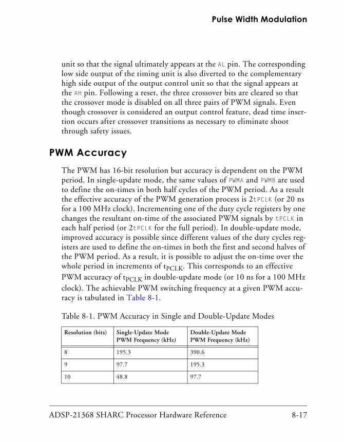
ADSP-21368 SHARC Processor Hardware Reference 8-17
Pulse Width Modulation
unit so that the signal ultimately appears at the AL pin. The corresponding low side output of the timing unit is also diverted to the complementary high side output of the output control unit so that the signal appears at the AH pin. Following a reset, the three crossover bits are cleared so that the crossover mode is disabled on all three pairs of PWM signals. Even though crossover is considered an output control feature, dead time inser-tion occurs after crossover transitions as necessary to eliminate shoot through safety issues.
PWM AccuracyThe PWM has 16-bit resolution but accuracy is dependent on the PWM period. In single-update mode, the same values of PWMA and PWMB are used to define the on-times in both half cycles of the PWM period. As a result the effective accuracy of the PWM generation process is 2tPCLK (or 20 ns for a 100 MHz clock). Incrementing one of the duty cycle registers by one changes the resultant on-time of the associated PWM signals by tPCLK in each half period (or 2tPCLK for the full period). In double-update mode, improved accuracy is possible since different values of the duty cycles reg-isters are used to define the on-times in both the first and second halves of the PWM period. As a result, it is possible to adjust the on-time over the whole period in increments of tPCLK. This corresponds to an effective PWM accuracy of tPCLK in double-update mode (or 10 ns for a 100 MHz clock). The achievable PWM switching frequency at a given PWM accu-racy is tabulated in Table 8-1.
Table 8-1. PWM Accuracy in Single and Double-Update Modes
Resolution (bits) Single-Update Mode PWM Frequency (kHz)
Double-Update Mode PWM Frequency (kHz)
8 195.3 390.6
9 97.7 195.3
10 48.8 97.7

PWM Registers
8-18 ADSP-21368 SHARC Processor Hardware Reference
PWM RegistersThe registers described below control the operation and provide the status of pulse width modulation on the ADSP-21367/8/9 and ADSP-2137x processors. For more information, see “Pulse Width Modulation Regis-ters” on page A-78.
• PWM global control register. The PWMGCTL register enables or dis-ables the four PWM groups in any combination. This provides synchronization across the four PWM groups. This 16-bit, read/write register is located at address 0x3800.
• PWM global status register. The PWMGSTAT register provides the status of each PWM group and is located at address 0x3801. The bits in this register are W1C-type (write one-to-clear).
• PWM control registers. The PWMCTL3–0 registers are used to set the operating modes of each PWM block. These registers also allow programs to disable interrupts from individual groups.
• PWM status registers. The PWMSTAT3–0 registers are 16-bit read-only registers report the status of the phase and mode for each PWM group.
11 24.4 48.8
12 12.2 24.4
13 6.1 12.2
14 3.05 6.1
Table 8-1. PWM Accuracy in Single and Double-Update Modes (Cont’d)
Resolution (bits) Single-Update Mode PWM Frequency (kHz)
Double-Update Mode PWM Frequency (kHz)

ADSP-21368 SHARC Processor Hardware Reference 8-19
Pulse Width Modulation
• PWM period registers. The PWMPERIOD3–0 registers are 16-bit, read/write registers that control the period of the four PWM groups.
• PWM dead time registers. The PWMDT3–0 registers are 16-bit, read/write registers that are used to set the switching dead time.
• PWM channel A and B duty control registers. The PWMA3–0 and PWMBx registers directly control the duty cycles of the two pairs of PWM output signals on the pwm_ah to pwm_cl pins when not in switch reluctance mode.
• PWM output enable registers. The PWMSEG3–0 registers are 16-bit read/write registers that are used to control the output signals of the four PWM groups.
• PWM channel A and B low side duty control registers. In non-paired mode, the PWMAL3–0 and PWMBL3–0 registers are used to program the low side duty cycle of the two pairs of PWM output signals. These can be different for the high side cycles.
• PWM output polarity select registers. The PWMPOL3–0 registers are 16-bit read/write registers that are used to determine whether the polarity of the generated PWM signals are active high or active low. The polarity values can be changed on-the-fly if required, provided the change is done a few cycles before the next period change.
Duty CyclesThe PWMAx and PWMBx registers directly control the duty cycles of the two pairs of PWM output signals on the pwm_ah to pwm_cl pins when not in switch reluctance mode.

PWM Registers
8-20 ADSP-21368 SHARC Processor Hardware Reference
• The two’s-complement integer value in the PWMAx registers controls the duty cycle of the signals on the pwm_ah and pwm_al pins.
• The two’s-complement integer value in the PWMBx registers control the duty cycle of the signals on pwm_bh and pwm_bl pins.
The duty cycle registers are programmed in two’s-complement integer counts of the fundamental time unit, tPCLK, and define the desired on-time of the high side PWM signal produced by the three-phase timing unit over half the PWM period. The duty cycle register range is from
(–PWMPERIOD ÷ 2 – PWMDT) to (+PWMPERIOD ÷ 2 + PWMDT)
which, by definition, is scaled such that a value of 0 represents a 50% PWM duty cycle. The switching signals produced by the three-phase tim-ing unit are also adjusted to incorporate the programmed dead time value in the PWMDT register. The three-phase timing unit produces active low sig-nals so that a low level corresponds to a command to turn on the associated power device.
Output EnableThe PWMSEG register contains six bits (0 to 5) that can be used to individu-ally enable or disable each of the six PWM outputs. If the associated bit of the PWMSEG register is set (=1), then the corresponding PWM output is dis-abled, regardless of the value of the corresponding duty cycle register. This PWM output signal remains disabled as long as the corresponding enable/disable bit of the PWMSEGx register is set. Programs should imple-ment this function after the crossover function. After reset, all six enable bits of the PWMSEG register are cleared so that all PWM outputs are enabled (default). In the same manner as the duty cycle registers, the PWMSEG regis-ter is latched on the rising edge of the pwm_pwmsync_out signal. Therefore, in single-update mode, changes to this register only become effective at the start of each PWM cycle. In double-update mode, the PWMSEG register can also be updated at the midpoint of the PWM cycle.

ADSP-21368 SHARC Processor Hardware Reference 8-21
Pulse Width Modulation
Programming Example The following program shows the four steps used to configure a PWM module.
Listing 8-1. Generic PWM Configuration Example
#include "def21369.h"
.global start;
/* define for PWM frequency used in PWMPERIOD0 */
#define fPWM 0x1388; /* 200MHz/2(20kHz) => 50us */
.section/pm seg_pmco;
start:
call default_int_enable;
call PWM_setup;
call PWM_enables;
nop;
finish: jump finish;
start.end: nop;
/* enable interrupts */
default_int_enable:
LIRPTL = 0;
IRPTL = 0;
bit set MODE1 IRPTEN; /* Global interrupt enable
bit set LIRPTL P13IMSK; /* Enable PWM default interrupt -
location 13 */
default_int_enable.end: rts;
/* PWM setup registers */
PWM_setup:

Programming Example
8-22 ADSP-21368 SHARC Processor Hardware Reference
/* 1. Configure frequency */
ustat3=fPWM; /* fPCLK/2xfPWM */
dm(PWMPERIOD0)=ustat3; /* PWM Period Register for switching
frequency (unsigned integer) */
/* 2. Configure duty cycles Width=[period/2] + duty program in
the two’s-complement of the high side width for individual con-
trol this only programs AH signal. If PWMAL0 is not programmed
then the AL and AH signals have the same duty cycle */
ustat3=0; /* PWM Channel A Duty Control
(two’s-complement integer) */
dm(PWMA0)=ustat3; /* Set up the duty cycle register to 0
(50% duty cycle) */
ustat3 = 0x63C; /* two’s-complement of 0x9C4 = 0x63C - 80%
high - 20% low */
dm(PWMAL0)=ustat3; /* PWM Channel AL Duty Control */
/* 3. Configure Dead Time */
ustat3=0x0; /* PWM Dead Time Register (unsigned integer) */
dm(PWMDT0)=ustat3;
/* 4. Configure Polarity (this can be changed on the fly
after the PWM port is enabled) */
ustat3=0; /* PWM Polarity Select Register */
bit set ustat3 PWM_POL1AL | PWM_POL1AH; /* Enables high polarity
A output /*
dm(PWMPOL0)=ustat3;
PWM_setup.end: nop;

ADSP-21368 SHARC Processor Hardware Reference 8-23
Pulse Width Modulation
/* PWM enables */
PWM_enables:
ustat3=dm(SYSCTL); /* System Control Register */
bit set ustat3 PWM0EN | PPFLGS;
dm(SYSCTL)=ustat3; /* Selects AD11–8 in PWM0 mode instead
of PP mode */
ustat3=dm(PWMSEG0); /* PWM Output Enable. Should probably be
changed to PWM Output Disable since you
write it to disable it. */
bit set ustat3 PWM_BH | PWM_BL; /* disables B outputs */
dm(PWMSEG0)=ustat3;
ustat3=dm(PWMCTL0); /* PWM0 Control Register
ustat3=0;
dm(PWMCTL0)=ustat3; /* Enables edge-aligned, individual pair
mode with single update and no
interrupt */
ustat3=dm(PWMGCTL); /* PWM General Control Register */
bit set ustat3 PWM_EN0 | PWM_DIS1 | PWM_DIS2 | PWM_DIS3 |
PWM_SYNCEN0 | PWM_SYNCDIS1| PWM_SYNCDIS2| PWM_SYNCDIS3;
dm(PWMGCTL)=ustat3; /* Enables only PWM 0 and its internal
timer; Disables other PWMs globally. The
write to PWMGCTL will kick off the
transfer */
PWM_enables.end: rts;
idle;

Programming Example
8-24 ADSP-21368 SHARC Processor Hardware Reference

ADSP-21368 SHARC Processor Hardware Reference 9-1
9 S/PDIF TRANSMITTER/RECEIVER
S/PDIF (Sony/Philips Digital Interface) is a standard audio data transfer format that allows the transfer of digital audio signals from one device to another without having to be converted to an analog signal. The ADSP-21367/8/9 and ADSP-2137x processors have AES3-compliant S/PDIF receivers/transmitters that allow programs to interface to other S/PDIF devices.
This chapter provides information on the function of the S/PDIF module in the ADSP-21367/8/9 and ADSP-2137x SHARC processors. It is important to be familiar with the serial digital audio interface standards IEC-60958, EIAJ CP-340, AES3, and AES11.
The S/PDIF receiver and transmitter reside in the digital audio interface (DAI). This allows applications to use the serial ports and/or the external DAI pins to interface to other S/PDIF devices. This can include using the receiver to decode incoming bi-phase encoded audio streams and passing them through the SPORTs to internal memory for processing or using the transmitter to encode audio or digital data and transfer it to another S/PDIF receiver in the audio system. Other features include:
• Managing user status information and providing error-handling capabilities in both the receiver and transmitter.
• Transmitting a bi-phase encoded signal that may contain any num-ber of audio channels (compressed or linear PCM) or encoded data streams.

AES3/SPDIF Stream Format
9-2 ADSP-21368 SHARC Processor Hardware Reference
• In regards to handling channel status information, the SPDIF transmitter can operate in standalone and full serial modes. In stan-dalone mode, channel status bits, user bits, and validity bits are taken from the corresponding buffers or control register. In full serial mode, all these bits are transferred with data bits from the SDATA pin. This allows programs to have control over the status fields and the ability to pass on status information which may have been supplied from an encoder, for instance.
AES3/SPDIF Stream FormatThe data carried by the SPDIF interface is transmitted serially. In order to identify the assorted bits of information the data stream is divided into frames, each of which are 64 time slots (or 128 unit intervals1) in length (Figure 9-1). Since the time slots correspond with the data bits, the frame is often described as being 64 bits in length.
1 The unit interval is the minimum time interval between condition changes of a data transmission sig-nal.
Figure 9-1. S/PDIF Block Structure
CHANNEL1X Y
CHANNEL2 Z Y
CHANNEL1
CHANNEL2
CHANNEL1
CHANNEL2X Y
START OFBLOCK
FRAME 0FRAME 191 FRAME 1
SUBFRAME1
SUBFRAME2

ADSP-21368 SHARC Processor Hardware Reference 9-3
S/PDIF Transmitter/Receiver
A frame is uniquely composed of two subframes. The first subframe nor-mally starts with preamble X. However, the preamble changes to preamble Z once every 192 frames. This defines the block of frames structure used to organize the channel status information. The second subframe always starts with preamble Y.
Subframe FormatEach frame consists of two subframes. Figure 9-2 shows an illustration of a subframe, which consists of 32 time slots numbered 0 to 31. A subframe is 64 unit intervals in length. The first four time slots of each subframe carry the preamble information. The preamble marks the subframe start and identifies the subframe type. The next 24 time slots carry the audio sample data, which is transmitted in a 24-bit word with the least signifi-cant bit (LSB) first. When a 20-bit coding range is sufficient, time slots 8 to 27 carry the audio sample word with the LSB in time slot 8. Time slots 4 to 7 may be used for other applications. Under these circumstances, the bits in time slots 4 to 7 are designated auxiliary sample bits. If the source provides fewer bits than the interface allows (either 20 or 24), the unused LSBs are set to logic 0.
This functionality is important when using the SPDIF receiver in com-mon applications where there are multiple types of data to handle. If there are PCM audio data streams as well as encoded data streams, for example a CD audio stream and a DVD audio stream with encoded data, there is a danger of incorrectly passing the encoded data directly to the DAC. This results in the ‘playing’ of encoded data as audio, causing loud odd noises to be played. The non-audio flag provides an easy method to mark the this type of data.
After the audio sample word, there are four final time slots which carry:
1. Validity bit (time slot 28). The validity bit is logic 0 if the audio sample word is suitable for conversion to an analog audio signal, and logic 1 if it is not. This bit is set if the CHST_BUF_ENABLE bit

AES3/SPDIF Stream Format
9-4 ADSP-21368 SHARC Processor Hardware Reference
and the VALIDITY_A (VALIDITY_B for channel 2) bit is set in the SPDIF_TX_CTL register. This bit is also set if the corresponding bit given with the sample is set.
2. User data bit (time slot 29). This bit carries user-specified infor-mation that may be used in any way. This bit is set if the corresponding bit given with the left/right sample is set.
3. Channel status bit (time slot 30). The channel status for each audio signal carries information associated with that audio signal, making it possible for different channel status data to be carried in the two subframes of the digital audio signal. Examples of informa-tion to be carried in the channel status are: length of audio sample words, number of audio channels, sampling frequency, sample address code, alphanumeric source and destination codes, and emphasis.
Figure 9-2. Subframe Format
PR
EA
MB
LE
LS
B
MS
B
24-BIT AUDIO WORD
VAL
IDIT
Y
US
ER
CH
AN
NE
L
PAR
ITY
0 3 4 27 28 29 30 31
DA
TA
STA
TU
S
PR
EA
MB
LE
LS
B
MS
B
20-BIT AUDIO WORD
VAL
IDIT
Y
US
ER
CH
AN
NE
L
PAR
ITY
0 3 4 27 28 29 30 31
DA
TA
STA
TU
S
7 8
AU
XIL
IAR
YS
AM
PL
EB
ITS

ADSP-21368 SHARC Processor Hardware Reference 9-5
S/PDIF Transmitter/Receiver
Channel status information is organized in 192-bit blocks, subdi-vided into 24 bytes. The first bit of each block is carried in the frame with preamble Z.
For convenience, the first five bytes of the channel status may be written all at once to control registers for both channels A and B (SPDIF_TX_CTL, SPDIF_TX_CHSTA, and SPDIF_TX_CHSTB). If the CHST_BUF_ENABLE bit is set in the SPDIF_TX_CTL register, the appro-priate CS bit is ORed into the channel status bit of the 192-word frame. In addition, the CS bit can also be provided along with the data samples to be transmitted.
4. Parity bit (time slot 31). The parity bit indicates that time slots 4 to 31 inclusive will carry an even number of ones and an even number of zeros (even parity). The parity bit is automatically gen-erated for each subframe and inserted into the encoded data.
The two subframes in a frame can be used to transmit two channels of data (channel 1 in subframe 1, channel 2 in subframe 2) with a sample rate equal to the frame rate. Alternatively, the two subframes can carry successive samples of the same channel of data, but at a sample rate that is twice the frame rate. This is called single-channel, double-frequency (SCDF). For more information, see “Single-Channel, Double-Sampling Frequency Mode” on page 9-21.
Channel CodingTo minimize the direct-current (dc) component on the transmission line, to facilitate clock recovery from the data stream, and to make the interface insensitive to the polarity of connections, time slots 4 to 31 are encoded in bi-phase mark.

AES3/SPDIF Stream Format
9-6 ADSP-21368 SHARC Processor Hardware Reference
Each bit to be transmitted is represented by a symbol comprising two con-secutive binary states. The first state of a symbol is always different from the second state of the previous symbol. The second state of the symbol is identical to the first if the bit to be transmitted is logic 0. However, it is different if the bit is logic 1.
Figure 9-3 shows that the ones in the original data end up with mid cell transitions in the bi-phase mark encoded data, while zeros in the original data do not. Note that the bi-phase mark encoded data always has a transi-tion between bit boundaries.
PreamblesPreambles are specific patterns that provide synchronization and identify the subframes and blocks. To achieve synchronization within one sam-pling period and to make this process completely reliable, these patterns violate the bi-phase mark code rules, thereby avoiding the possibility of data imitating the preambles.
Figure 9-3. Bi-phase Mark Encoding
10 1 1 0 0
CLOCK(2 TIMES BIT RATE
DATA
BI-PHASE-MARKDATA

ADSP-21368 SHARC Processor Hardware Reference 9-7
S/PDIF Transmitter/Receiver
A set of three preambles, shown in Table 9-1, are used. These preambles are transmitted in the time allocated to four time slots at the start of each subframe (time slots 0 to 3) and are represented by eight successive states. The first state of the preamble is always different from the second state of the previous symbol (representing the parity bit).
Like bi-phase code, the preambles are dc free and provide clock recovery. They differ in at least two states from any valid bi-phase sequence.
S/PDIF TransmitterThe S/PDIF transmitter resides within the DAI, and its inputs and out-puts can be routed through the signal routing unit (SRU1). It receives audio data in serial format, encloses the specified user status information, and converts it into the bi-phase encoded signal. The serial data input to the transmitter can be formatted as left-justified, I2S, or right-justified with word widths of 16, 18, 20 or 24 bits.
The serial data, clock, external sync signal, and frame sync inputs to the S/PDIF transmitter are routed through SRU1. They can come from a variety of sources such as the SPORTs, external pins, the precision clock generators (PCG), or the sample rate converters (SRC). The signal routing is selected in the SRU1 control registers. For more information, see “DAI/SRU1 Connection Groups” on page 4-18.
Table 9-1. Preambles
Preamble Preceding state 0 Preceding state 1 Description
X 11100010 00011101 Subframe 1
Y 11100100 00011011 Subframe 2
Z 11101000 00010111 Subframe 1 and block start

S/PDIF Transmitter
9-8 ADSP-21368 SHARC Processor Hardware Reference
The S/PDIF transmitter output may be routed to an output pin through SRU1 and then routed to another S/PDIF receiver or to components for off-board connections to other S/PDIF receivers. The output is also avail-able to the S/PDIF receiver for loop-back testing through SRU1.
Two output data formats are supported by the transmitter: two channel mode and single channel double frequency (SCDF) mode. The output for-mat is determined by the transmitter control register (DITCTL). For more information, see “Transmitter Control Register (DITCTL)” on page A-86.
In two channel mode, the left channel (channel A) is transmitted when the LRCLK is high and the right channel (channel B) is transmitted when the LRCLK is low.
Figure 9-4. S/PDIF Transmitter Block Diagram
TRANSMITTERCONTROLREGISTER
SERIAL TOPARALLEL
CONVERTER
TRANSMITTER
BI-PHASECLOCK
GENERATOR
SCLK (BCLK)
SDATA
LRCLK (FS)
TX_CLK
TX_BI-PHASE_CLOCK
BI-PHASE_OUTAUDIO
SAMPLES
CONTROL
EXT_SYNC

ADSP-21368 SHARC Processor Hardware Reference 9-9
S/PDIF Transmitter/Receiver
In SCDF mode, the transmitter sends successive audio samples of the same signal across both subframes, instead of channel A and B. This mode also allows programs to select which channel is sent when using bits in the S/PDIF transmit control register. The channel status bits are set to pro-vide the downstream receiver with information about which channel is used.
Channel StatusIn addition to encoding the audio data in the bi-phase format, the trans-mitter also provides a way to easily add the channel status information to the outgoing bi-phase stream. There are status registers in the transmitter that correspond to each channel or subframe. Byte 0 for each channel A and B reside in the DITCTL register, and bytes 1–4 reside in the DITCHANxx registers. For more information, see “Transmitter Control Register (DITCTL)” on page A-86, “Left Channel Status for Subframe A Registers (DITCHANAx)” on page A-89 and “Right Channel Status for Subframe B Registers (DITCHANBx)” on page A-90.
The first five bytes of the channel status may be written all at once to the control registers for both A and B channels. As the data is serialized and transmitted, the appropriate bit is inserted into the channel status area of the 192-word frame. Validity bits for both channels may also be con-trolled by the transmitter control register. Optionally, the user bit, validity bit, and channel status bit are sent to the transmitter with each left/right sample. For each subframe the parity bit is automatically generated and inserted into the bi-phase encoded data. A mute control and support for double-frequency single-channel mode are also provided. The serial data input format may be selected as left-justified, I2S, or right-justified with 16-, 18-, 20- or 24-bit word widths. The over sampling clock is also selected by the transmitter control register.

S/PDIF Transmitter
9-10 ADSP-21368 SHARC Processor Hardware Reference
SRU1 Signals for the S/PDIF TransmitterTo use the transmitter, route the five required inputs using SRU1 as described below. Also, use SRU1 to connect the two outputs, bi-phase encoded output, and block start to the desired DAI (digital audio inter-face) pin.
DIT_CLK_I is the serial clock. It controls the rate at which serial data enters the S/PDIF module. This is typically 64 time slots1. The SCLK input to the S/PDIF transmitter is controlled by the 5-bit clock routing (SRU1 group A) register field SRU_CLK2[14:10] (DIT_CLK_I). This clock input can come from the SPORTS, the PCG, external pins, or from the S/PDIF receiver. By default it is connected to LOGIC_LEVEL_LOW. For more infor-mation, see “Group A Connections—Clock Signals” on page 4-19.
DIT_DAT_I provides serial data. The format of the serial data can be I2S and right/left-justified. The SDATA input to the S/PDIF transmitter is con-trolled by the 6-bit serial data routing (SRU1 group B) register field SRU_DAT4[5:0] (DIT_DAT_I). The data input can come from the SPORTs, the SRC, external pins, or from the S/PDIF receiver. By default, SDATA is connected to external pin 0. For more information, see “Group B Connec-tions—Data Signals” on page 4-25.
DIT_FS_I is the frame sync input to the S/PDIF transmitter. It is con-trolled by the 5-bit LRCLK routing (SRU1 group C) register field SRU_FS2[14:10]. The frame sync input can come from the SPORTs, the PCGs, external pins, or from the S/PDIF receiver. By default the frame sync is connected to LOGIC_LEVEL_LOW. For more information, see “Group C Connections—Frame Sync Signals” on page 4-31.
1 Timing for the S/PDIF format consists of time slots, unit intervals, subframes and frames. For a com-plete explanation of S/PDIF timing, see one of the digital audio interface standards listed at the begin-ning of this chapter.

ADSP-21368 SHARC Processor Hardware Reference 9-11
S/PDIF Transmitter/Receiver
DIT_HFCLK_I is the oversampling clock. This clock is divided down according to the FREQMULT bit in the transmitter control register to gener-ate the bi-phase clock. It can also be selected from various sources since it is routed through SRU1. The TX_CLK input to the S/PDIF transmitter is controlled by the 5-bit clock routing (SRU1 group A) register field SRU_CLK3[29:25] (DIT_HFCLK_I). This clock input can come from the SPORTS, the PCG, external pins, or from the S/PDIF receiver. By default TX_CLK is connected to LOGIC_LEVEL_LOW. For more information, see “Group A Connections—Clock Signals” on page 4-19.
DIT_EXTSYNC_I is a clock input to the SPDIF transmitter and is con-trolled by the 5-bit clock routing (SRU1 group A) register field SRU_CLK4[19:15] (SPDIF_TX_EXT_SYNC). This clock can come from any of 20 external DAI pins. By default it is connected to LOGIC_LEVEL_LOW.
DIT_O is the bi-phase encoded data stream. It can be routed to any of the external pins or to the S/PDIF receiver for loop-back testing through SRU1. The SRU_PINx registers control this routing. For more information, see “Group D Connections—Pin Signal Assignments” on page 4-36.
BLK_START indicates the last frame of the current block. This is high for the entire duration of the frame. The BLK_START output can be routed to any of the external pins controlled by the SRU_PINx registers. This can also be connected to the DAI interrupts [31–22] using the SRU_MISCx reg-isters. Use of this signal is optional.

S/PDIF Transmitter
9-12 ADSP-21368 SHARC Processor Hardware Reference
S/PDIF Transmitter RegistersThe SPDIF transmitter contains registers that are used to enable/disable the transmitter, to manage its operation, and to report status. The regis-ters are described below.
• DITCTL is the S/PDIF transmit control register. This 32-bit read/write register is located at address 0x24A0. It is used to enable the transmitter, control mute, over sampling, mode and data for-mat. This register is described in detail in “Transmitter Control Register (DITCTL)” on page A-86.
• DITCHANAx and DITCHANBx are the S/PDIF channel A and B transmit status registers. These 32-bit read/write registers, located at addresses 0x24A1 and 0x24A2, provide status informa-tion for transmitter subframe A and B. These registers are described in detail in “Left Channel Status for Subframe A Regis-ters (DITCHANAx)” on page A-89 and “Right Channel Status for Subframe B Registers (DITCHANBx)” on page A-90. These regis-ters are used in standalone mode only.
• DITUSRBITAx and DITUSRBITBx are the user bit buffers. Once programmed, they are used only for the next block of data. This allows programs to change the user bit information with every block of data. After writing to the appropriate registers to change the user bits for the next block, DITUSRBITAx and DITUSRBITBx must be written to enable the use of these bits. These registers are used in standalone mode only.
Modes of OperationThe SPDIF transmitter can operate in standalone and full serial modes. The following sections describe these modes in detail.

ADSP-21368 SHARC Processor Hardware Reference 9-13
S/PDIF Transmitter/Receiver
Standalone Mode
This mode is selected by setting bit 9 in the DITCTL register. In this mode, the block start bit (indicating start of a frame) is generated internally. The channel status bits come from the channel status buffer registers (DITCHA-NAx and DITCHANBx). The user status bits come from the user bits buffers (DITUSRBITAx and DITUSRBITBx). The channel status buffer must be pro-grammed before the SPDIF transmitter is enabled and used for all the successive blocks of data.
Once the user bits buffer registers (DITUSRBITA0-5 and DITUSRBITB0-5) are programmed, they are used only for the next block of data. This allows programs to change the user bit information in every block of data. After writing to the required user bit buffer registers to change the user bits for the next block, these registers must be rewritten to enable the use of these bits in the next block. The validity bit for channel A and B are taken from bit 10 and bit 11 of the DITCTL register. In this mode only audio data comes from the SDATA pin. All other data, including the status bit and block start bit is either generated internally or taken from the internal register.
Full Serial Mode
This mode is selected by clearing bit 9 in the DITCTL register. In this mode all the status bits, audio data and the block start bit (indicating start of a frame), come through the SDATA pin. The transmitter should be enabled after or at the same time as all of the other control bits.

S/PDIF Transmitter
9-14 ADSP-21368 SHARC Processor Hardware Reference
Structure of the Serial Input DataFigure 9-5 shows the format of data that is sent to the S/PDIF transmitter using a 24-bit I2S interface. The upper 24 bits (bits 8 through 31) contain the audio data. Bits 3–7 are used to transmit status information and to generate preambles and or headers. Bits 0 through 3 are empty.
When I2S format is used with 20-bit or 16-bit data, the audio data should be placed from the MSB of the 24-bit audio data.
Figure 9-5. Data Packing for I2S and Left-Justified Format
Figure 9-6. Data Packing for Right-Justified Format, 24 Bits
Bits 31–8: 24-Bit Audio Data 7 6 5 4 BITS 3–0
Padding (zero)BLK_STRT
Channel Status
User DataValidity Bit
Bits 27–4: 24-Bit Audio Data 3 2 1 0
Channel Status
User Data
Validity Bit
Block Status

ADSP-21368 SHARC Processor Hardware Reference 9-15
S/PDIF Transmitter/Receiver
Figure 9-7. Data Packing for Right-Justified Format, 20 Bits
Figure 9-8. Data Packing for Right-Justified Format, 18 Bits
Figure 9-9. Data Packing for Right-Justified Format, 16 Bits
Bits 27–8: 20-Bit Audio Data 7 6 5 4 BITS 3–0
Padding (zero)Block Status
Channel Status
User DataValidity Bit
Bits 27–10: 18-Bit Audio Data 9 8 7 6 BITS 5–0
Padding (zero)Block Status
Channel Status
User DataValidity Bit
Bits 27–12: 16-Bit Audio Data 11 10 9 8 BITS 7–0
Padding (zero)Block Status
Channel Status
User DataValidity Bit

S/PDIF Receiver
9-16 ADSP-21368 SHARC Processor Hardware Reference
S/PDIF ReceiverThe S/PDIF receiver is compliant with all common serial digital audio interface standards including IEC-60958, IEC-61937, AES3, and AES11. These standards define a group of protocols that are commonly associated with the S/PDIF interface standard defined by AES3, which was devel-oped and is maintained by the Audio Engineering Society. AES3 effectively defines the data and status bit structure of an S/PDIF stream. AES3-compliant data is sometimes referred to as AES/EBU compliant. This term highlights the adoption of the AES3 standard by the European Broadcasting Union. The S/PDIF receiver in the ADSP-21367/8/9 and ADSP-2137x processors receives an S/PDIF bi-phase encoded stream and decodes it into an I2S serial data format, and provides the programmer with several methods of managing the incoming status bit information.
The input to the receiver is a bi-phase encoded signal that may contain two audio channels (compressed or linear PCM) or non-audio data. The receiver decodes the single bi-phase encoded stream, producing an I2S-compatible serial data output that consists of a serial clock (SCLK), a left/right clock (FS), and data (channel A/B).
The receiver can recover the clock from the bi-phase encoded stream using either a dedicated on-chip digital phased-locked loop (PLL) or an external analog PLL. (The dedicated on-chip digital PLL is separate from the PLL that supplies the core clock to the ADSP-213xx processor core.)
The S/PDIF receiver input stream can be selected from any of the DAI pins, DAI_P20–1, or from the output of the S/PDIF transmitter for loop-back testing using signal routing group C. The first five bytes of the channel status are identified and stored in dedicated status registers for both A and B channels. The registers are DIR_CHANL and DIR_CHANR. As the serial data is received, the appropriate bits (first five bytes – bit 0 through bit 39) are updated from the 192-word frame. If the channel status bits change, an interrupt may optionally be generated to notify the core.

ADSP-21368 SHARC Processor Hardware Reference 9-17
S/PDIF Transmitter/Receiver
The receiver also detects errors in the S/PDIF stream. These error bits are stored in the status register, which can be read by the core. Optionally, an interrupt may be generated to notify the core on error conditions. The extracted serial data is transmitted on the data pin in I2S format. The extracted clock, frame sync, and data are routed through SRU1.
The S/PDIF receiver receives any S/PDIF stream with a sampling fre-quency range of 32 kHz – 15% to 192 kHz + 15% range.
The serial output from the receiver is 24-bit I2S serial data which con-forms to the format shown in Figure 9-5 on page 9-14.
S/PDIF Receiver RegistersThe S/PDIF receiver uses the registers described in the following sections. More detail can be found in “Sony/Philips Digital Interface Registers” on page A-86.
DIRCTL is the receiver control register. It is a 32-bit, read/write register located at address 0x24A8 and is used to enable the receiver, control mute, PLL and SCDF mode. This register is described in detail in “Receiver Control Register (DIRCTL)” on page A-92.
DIRSTAT is the receiver status register. It is a 32-bit, read-only register that is used to store the error bits. The error bits are sticky on read. Once they are set, they remain set until the register is read. This register also contains the lower byte of the 40-bit channel status information.
DIRCHANL, DIRCHANR are the channel status for the subframes regis-ters. They provide status information for subframe A (left channel) bytes 1, 2, 3, and 4 and subframe B (right channel) bytes 1, 2, 3, and 4. These 32-bit, read/write registers are located at address 0x24AA and 0x24AB. See also “Left Channel Status for Subframe A Registers (DITCHANAx)” on page A-89 and “Right Channel Status for Subframe B Registers (DIT-CHANBx)” on page A-90.

S/PDIF Receiver
9-18 ADSP-21368 SHARC Processor Hardware Reference
SRU1 Receiver SignalsThe bi-phase encoded data and the external PLL clock inputs to the receiver are routed through the signal routing unit (SRU1). The extracted clock, frame sync, and data are also routed through SRU1.
The SRU1 inputs to the S/PDIF receiver are configured through the fol-lowing signals.
• SPDIF_PLLCLK_I is the external 512 x FS (frame sync) PLL clock input. This signal is controlled by the 5-bit clock routing reg-ister field SRU_CLK4[14:10] (Figure 4-16 on page 4-22). This clock input can come from the external pins connected to the external PLL.
• DIR_I is the bi-phase encoded data input. This signal is controlled by the 5-bit frame sync routing register field SRU_FS3[29:25] (Figure 4-16 on page 4-22). This data may be received from exter-nal pins or from the S/PDIF receiver.
The SRU1 outputs from the S/PDIF receiver are configured through the following signals.
• DIR_DAT_O is the extracted audio data output. This signal can be routed to any of the external pins or to one of the serial receivers (SPORT, input data port) through SRU1.
• DIR_CLK_O is the extracted receiver sample clock output. This signal can be routed to any of the external pins or to one of the serial receivers (SPORT, input data port) through SRU1.
• DIR_FS_O is the extracted receiver frame sync out. This signal can be routed to any of the external pins or to one of the serial receivers (SPORT, input data port) through SRU1.
ADSP-21368 SHARC Processor Hardware Reference 9-19
S/PDIF Transmitter/Receiver
• DIR_TDMCLK_O is the receiver TDM clock output. This signal can be routed to any of the external pins or to one of the serial receivers (SPORT, input data port) through SRU1.
• DIR_LRCLK_FB is the external PLL feedback point connection.
• DIR_LRCLK_REF is the external PLL reference point connection.
Phase-Locked LoopThe phase-locked loop for the AES3/SPDIF receiver is intended to recover the clock that generated the AES3/SPDIF bi-phase encoded stream. This clock is used by the receiver to clock in the bi-phase encoded data stream and also to provide clocks for either the serial ports, sample rate converter, or AES3/SPDIF transmitter. The recovered clock may also be used exter-nally to the chip for clocking D/A and A/D converters.
In order to maintain performance, jitter on the clock is sourced to several peripherals. Jitter on the recovered clock must be less than 200 ps and, if possible, less than 100 ps across all the sampling frequencies ranging from 27.2 kHz to 220.8 kHz (32 kHz – 15% and 192 kHz + 15%). Further-more, once the PLL achieves lock, it is able to vary ±15% in frequency over time. This allows for applications that do not use PLL unlocking.
The receiver can be used with the on-chip digital PLL or with an external analog PLL. There are various performance characteristics to consider when configuring for analog PLL mode, and more information can be found on the Analog Devices Web site.
Channel Status DecodingThe S/PDIF receiver processes compressed as well as non-linear audio data according to the supported standards. The following sections describe how the S/PDIF receiver handles different data.

Channel Status Decoding
9-20 ADSP-21368 SHARC Processor Hardware Reference
Compressed or Non-Linear Audio DataThe AES3/SPDIF receiver is required to detect compressed or non-linear audio data according to the AES3, IEC60958, and IEC61937 standards. Bit 1 of byte 0 in the DIR_B0CHAN register indicates whether the audio data is linear PCM, (bit 1 = 0), or non-PCM audio, (bit 1 = 1). If the channel status indicates non-PCM audio, the DIR_NOAUDIO bit flag is set. (This bit can be used to generate an interrupt.) The DIR_VALID bit (bit 3 in the DIRSTAT register) when set (=1) may indicate non-linear audio data as well. Whenever this bit is set, the VALIDITY bit flag in the SPDIF_RX_STAT regis-ter is also set.
The MPEG-2, AC-3, DTS, and AAC compressed data may be transmitted without setting either the DIR_VALID bit or bit 1 of byte 0. To detect this data, the IEC61937 and SPMTE 337M standards dictate that there be a 96-bit sync code in the 16-, 20- or 24-bit audio data stream. This sync code consists of four words of zeros followed by a word consisting of 0xF872 and another word consisting of 0x4E1F. When this sync code is detected, the DIR_NOAUDIO bit flag is set. If the sync code is not detected again within 4096 frames, the DIR_NOAUDIO bit flag is deasserted.
The last two words of the sync code, 0xF872 and 0x4E1F, are called the preamble-A and preamble-B of the burst preamble. Preamble-C of the burst preamble contains burst information and is captured and stored by the receiver. Preamble-D of the burst preamble contains the length code and is captured by the receiver. Even if the validity bit or bit 1 of byte 0 has been set, the receiver still looks for the sync code in order to record the preamble-C and D values. Once the sync code has not been detected in 4096 frames, the preamble-C and D registers are set to zero.
The SPDIF receiver supports the DTS stream. The DTS specifica-tions support frame sizes of 256, 512, 1024, 2048 and 4096. The on-chip SPDIF receiver supports the 256, 512 and 1024 DTS frames. The DTS test kit frames with 2048 and 4096 frame sizes

ADSP-21368 SHARC Processor Hardware Reference 9-21
S/PDIF Transmitter/Receiver
can be detected by adding the sync detection logic in software by using a software counter to check for the DTS header every 2048 and 4096 frames respectively.
Emphasized Audio DataThe receiver must indicate to the program whether the received audio data is emphasized using the channel status bits as detailed below.
• In professional mode, (bit 0 of byte 0 = 1), channel status bits 2–4 of byte 0 indicate the audio data is emphasized if they are equal to 110 or 111.
• In consumer mode, (bit 0 of byte 0 = 0), channel status bits 3–5 indicate the audio data is emphasized if they are equal to 100, 010 or 110.
If emphasis is indicated in the channel status bits, the receiver asserts the EMPHASIS bit flag. This bit flag is used to generate an interrupt as shown in “Error Handling” on page 9-22.
Single-Channel, Double-Sampling Frequency Mode
Single-channel, double-frequency mode (SCDF) is selected with the DIR_SCDF and DIR_SCDF_LR bits in the DIRCTL register. The DIR_B0CHANL/R bits in the DIRSTAT register also contain information about the SCDF mode. When the DIR_B0CHANL/R indicates single-channel, double-fre-quency mode, the two subframes of a frame carry successive audio samples of the same signal.

Error Handling
9-22 ADSP-21368 SHARC Processor Hardware Reference
Bits 0–3 of channel status byte 1 are decoded by the receiver to determine one of the following:
• 0111 = single-channel, double-frequency mode
• 1000 = single-channel, double-frequency mode – stereo left
• 1001 = single-channel, double-frequency mode – stereo right
Error HandlingThe following five types of errors can occur in the receiver and are reported on the error flag bits.
1. Lock Error. When bit 4 in the DIRSTAT register is set (=1), the PLL is locked.
2. Bi-phase Error. When bit 7 in the DIRSTAT register is set (=1), it indicates that a bi-phase error has occurred and the data sampled from the bi-phase stream may not be correct.
3. Parity Error. When bit 6 in the DIRSTAT register is set (=1), it indi-cates that the AES3/SPDIF stream was received with the correct even parity. When the DIR_PARITYERROR bit is low (=0), it indicates that an error has occurred and the parity is odd.
4. CRCC Error. The CRCCERROR bit is asserted high whenever the CRCC check of the DIR_B0CHANL/R bits fails. The CRCC check is only performed if the channel status bit 0 of byte 0 is high, indicat-ing professional mode.
5. No Stream Error. The DIR_NOSTREAM bit is asserted whenever the AES3/SPDIF stream is disconnected.
When the DIR_NOSTREAM bit is asserted and the audio data in the stream is linear PCM, the receiver performs a soft mute of the last valid sample from the AES3/SPDIF stream. A soft mute consists of taking the last valid

ADSP-21368 SHARC Processor Hardware Reference 9-23
S/PDIF Transmitter/Receiver
audio sample and slowly and linearly decrementing it to zero, over a period of 4096 frames. During this time, the PLL three-states the charge pump until the soft mute has been completed. If non-linear PCM audio data is in the AES3/SPDIF stream when the NOSTREAM bit is asserted, the receiver sends out zeros after the last valid sample.
When the DIR_LOCK bit is deasserted, it means that the PLL has become unlocked and the audio data is handled according to the DIR_NOAUDIO[1:0] bits in the DIRCTL register. When this happens, the receiver functions as follows.
• 00 = no action is taken with the audio data.
• 01 = the last valid audio sample is held.
• 10 = zeros are sent out after the last valid sample.
• 11 = soft mute of the last valid audio sample is performed (as if DIR_NOSTREAM is asserted).
This is valid only when linear PCM audio data is in the stream. When non-linear audio data is in the stream, this mode defaults to the case of DIR_NOAUDIO[1:0] bits = 10.
When a parity or bi-phase error occurs, the audio data is handled accord-ing to the DIR_BIPHASEERROR_CTL[1:0] bits in the following manner.
• 00 = no action is taken with the audio data.
• 01 = the last valid sample is held.
• 10 = the invalid sample is replaced with zeros.
The VALIDITY, NONAUDIO, NOSTREAM, BIPHERR, PARITY and LOCK bits are also stored in the receiver status register as W1C bits.

Interrupts
9-24 ADSP-21368 SHARC Processor Hardware Reference
InterruptsThe following error/status bits can be used to interrupt the processor core.
• The DIR_LOCK, DIR_VALID, DIR_NOSTREAM and DIR_NOAUDIO bits can generate interrupts. Parity errors and bi-phase errors are ORed together to form a PARITY_BIPHASE_ERROR interrupt. Whenever there is a change in channel status information, a CHANNEL_STAT_CHANGE interrupt occurs.
• The DIR_BIPHASEERROR and DIR_VALID interrupts are one PCLK pulse wide.
• All interrupts are processed through the interrupt controller which can generate an interrupt on the rising or falling edge of the signal.
DAI Programming ExamplesThe following examples show how the S/PDIF receiver and transmitter are programmed using the digital audio interface/SRU1.
S/PDIF Transmitter Programming GuidelinesThe following guidelines are intended to help in programming the S/PDIF transmitter.
Control Register
The DITCTL register contains control parameters for the S/PDIF transmit-ter. The control parameters include transmitter enable, mute information, oversampling clock division ratio, SCDF mode select and enable, serial data input format select and validity, and channel status buffer selects. By default, all the bits in this register are zero.

ADSP-21368 SHARC Processor Hardware Reference 9-25
S/PDIF Transmitter/Receiver
SRU1 Programming for Input and Output Streams
Signal routing unit 1 (SRU1) is used to connect the S/PDIF transmitter bi-phase data out to the output pins or to the S/PDIF receiver. The serial data input and the over sampling clock input also needs to be routed through SRU1. See For more information, see “Group A Connections—Clock Signals” on page 4-19 and “Group B Connections—Data Signals” on page 4-25.
Control Register Programming and Enable
After SRU1 programming is complete, if the channel status or validity buffer needs enabling, write to the buffers first with the required data and then enable the buffers using the DIT_CHANBUF bit in the DITCTL register. Also write other control values such as DIT_SMODEIN, and DIT_FREQ and enable the transmitter by setting the DIT_EN bit.
S/PDIF Receiver Programming GuidelinesThe following guidelines are intended to help in programming the S/PDIF receiver.
Control Register
The S/PDIF receiver is enabled at default to receive in two channel mode. Therefore, if the receiver is not used, programs should disable the digital PLL to avoid unnecessary switching. This is accomplished by writing into the DIR_PLLDIS bit (bit 7) in the DIRCTL register. In most cases, when the S/PDIF receiver is used, this register does not need to be changed. For a detailed description of this register, see “Receiver Control Register (DIRCTL)” on page A-92.
The DIRCTL register contains control parameters for the S/PDIF receiver. The control parameters include mute information, error controls, SCDF mode select and enable, and digital PLL disable.
DAI Programming Examples
9-26 ADSP-21368 SHARC Processor Hardware Reference
SRU1 Programming
The SRU1 needs to be programmed in order to connect the S/PDIF receiver to the output pins or any other peripherals and also for the input bi-phase stream.
Program the corresponding SRU1 registers to connect the above outputs to the required destination. See “SRU1 Receiver Signals” on page 9-18, “Group A Connections—Clock Signals” on page 4-19, and “Group C Connections—Frame Sync Signals” on page 4-31.
Control Register Programming
After SRU1 programming is complete, write to the SPDIF_RX_CTL register with control values, and enable the internal digital PLL by clearing the DIR_PLLDIS bit if it was cleared initially. At this point, the receiver attempts to lock.
Receiver Locking
Once the receiver is locked, the corresponding LOCK bit in the DIRSTAT reg-ister is set. This bit can be polled to detect the LOCK condition. Another option is to use the SPDIF_RX_LOCK_START interrupt in the DAI_IRPTL_H/L register. This triggers the DAI_INTH/L interrupt once the receiver is locked. From this point on, the S/PDIF starts producing extracted output serial data. The data is guaranteed to be correct only after the LOCK goes high.
Status Bits
After the receiver is locked, the other status bits in the receiver status (DIRSTAT) and the channel status (DIRCHANL/R) registers can be read. Inter-rupts can also be used with some status bits.

ADSP-21368 SHARC Processor Hardware Reference 9-27
S/PDIF Transmitter/Receiver
Interrupted Data Streams on the Receiver
When using the SPDIF receiver with data streams that are likely to be interrupted, (in other words unplugged and reconnected), it is necessary to take some extra steps to ensure that the SPDIF receiver’s digital PLL will re lock to the stream. The steps to accomplish this are described below.
1. Setup interrupts within the DAI so that the SPDIF RX can gener-ate an interrupt when the stream is reconnected.
2. Within the interrupt service routine (ISR), stop and restart the dig-ital PLL. This is accomplished by setting and then clearing bit 7 of the SPDIF receiver control register.
3. Return from the ISR and continue normal operation.
This method of resetting the digital PLL has been shown to provide extremely reliable performance when SPDIF inputs that are interrupted or unplugged momentarily occur.
The following procedure and the example code show how to reset the dig-ital PLL. Note that all of the SPDIF receiver interrupts are handled through the DAI interrupt controller. For more information, see “DAI/DPI Interrupt Controller” on page 4-65.
1. Initialize the No Stream Interrupt
/* Enable interrupts (globally) */
BIT SET MODE1 IRPTEN;
/* unmask DAI Hi=Priority Interrupt */
bit set imask DAIHI;
ustat1 = DIR_NOSTREAM_INT;
/* Enable no-stream Interrupt on Falling Edge. Interrupt
occurs when the stream is reconnected */
dm(DAI_IRPTL_FE) = ustat1;

DAI Programming Examples
9-28 ADSP-21368 SHARC Processor Hardware Reference
/* Enable Hi-priority DAI interrupt */
dm(DAI_IRPTL_PRI) = ustat1;
/* If more than 1 DAI interrupt is being used, it is neces-
sary to determine which interrupt occurred here */
/* Interrupt Service Routine for the DAI Hi-Priority Inter-
rupt. This ISR triggered when the DIR sets no_stream bit */
_DAIisrH:
2. Reset the Digital PLL Inside of the ISR
r8=dm(DAI_IRPTL_H); /* Reading DAI_IRPTL_H
clears interrupt */
ustat2=dm(DIRCTL);
bit set ustat2 DIR_PLLDIS; /* bit_7 disables Dpll only */
dm(DIRCTL)=ustat2;
bit clr ustat2 DIR_PLLDIS; /*reenable the digital pll */
dm(DIRCTL)=ustat2;

ADSP-21368 SHARC Processor Hardware Reference 10-1
10 ASYNCHRONOUS SAMPLE RATE CONVERTER
Sample rate conversion is the process of converting a digital signal from one sampling rate to another, while modifying the information that is car-ried by the signal as little as possible.
Sample rate conversion is useful because different systems use different sampling rates for a variety reasons. Because the physics of sampling require a minimum sampling rate, other factors determine the actual rates used. For example, different audio systems can use rates of 44.1, 48, and 96 kHz and programs need to transfer source material between these sys-tems. Just replaying the existing data at the new rate does not work — it introduces large changes in pitch (for audio) and movement as well (for video), plus it cannot be done in real time.
The asynchronous sample rate converter (SRC), as it is implemented in the ADSP-21367/8/9 and ADSP-2137x processors, is used to perform asynchronous sample rate conversion across independent stereo channels without using any internal processor resources. Furthermore, the SRC blocks can be configured to operate together to convert multichannel audio data without phase mismatches. Finally, the SRC is used to clean up audio data from jittery clock sources such as the S/PDIF receiver.
The SRC contains four blocks (SRC0–3). It also is the same core that is used in the Analog Devices AD1896 192 kHz Stereo Asynchronous Sam-ple Rate Converter. The top-level block diagram of the SRC module is shown in Figure 10-4 on page 10-9.
The SRC has a 3-wire interface for the serial input and output ports that supports left-justified, I2S, and right-justified (16-, 18-, 20-, 24-bit) modes. Additionally, the serial interfaces support time-division

Theory of Operation
10-2 ADSP-21368 SHARC Processor Hardware Reference
multiplexing (TDM) mode for daisy-chaining multiple SRCs to a proces-sor. The serial output data is dithered down to 20, 18, or 16 bits when 20-, 18-, or 16-bit output data is selected.
Theory of OperationThe SRC sample rate converts the data from the serial input port to the sample rate of the serial output port. The sample rate at the serial input port can be asynchronous with respect to the output sample rate of the output serial port.
Conceptually, the SRC interpolates the serial input data by a rate of 220 and samples the interpolated data stream by the output sample rate. In practice, a 64-tap FIR filter with 220 poly phases, a FIFO, a digital-servo loop that measures the time difference between the input and output sam-ples within 5 ps, and a digital circuit to track the sample rate ratio are used to perform the interpolation and output sampling. The digital-servo loop and sample rate ratio circuit automatically track the input and output sample rates.
The digital-servo loop measures the time difference between the input and output sample rates within 5 ps. This is necessary in order to select the correct polyphase filter coefficient. The digital-servo loop has excellent jit-ter rejection for both input and output sample rates as well as the master clock. The jitter rejection begins at less than 1 Hz. This requires a long settling time whenever the SRC is enabled or when the input or output sample rate changes.
To reduce the settling time when the SRC is enabled or there is a change in the sample rate, the digital-servo loop enters the fast settling mode. When the digital-servo loop has adequately settled in the fast mode, it switches into the normal or slow settling mode and continues to settle until the time difference measurement between input and output sample rates is within 5 ps. During fast mode, the MUTE_OUT signal is asserted high.

ADSP-21368 SHARC Processor Hardware Reference 10-3
Asynchronous Sample Rate Converter
Normally, the MUTE_OUT signal is connected to the MUTE_IN signal. The MUTE_IN signal is used to softly mute the SRC upon assertion and softly stop muting the SRC when it is deasserted.
The sample rate ratio circuit is used to scale the filter length of the FIR fil-ter for decimation. Hysteresis in measuring the sample rate ratio is used to avoid oscillations in the scaling of the filter length, which would cause dis-tortion on the output.
However, when multiple SRCs are used with the same serial input port clock and the same serial output port clock, the hysteresis causes different group delays between multiple SRCs. A phase-matching mode feature was added to the SRC to address this problem. In phase-matching mode, one SRC, (the master), transmits its sample rate ratio to the other SRCs, (the slaves), so that the group delay between the multiple SRCs remains the same.
Asynchronous sample rate conversion is converting data from one clock source at a sample rate to another clock source at the same or a different sample rate. The simplest approach to an asynchronous sample rate con-version is the use of a zero-order hold between the two samplers shown in Figure 10-1. In the figure, fS_IN and fS_OUT are the input and output sampling frequencies, respectively, and T1 and T2 are the time periods that correspond to the input and output. In an asynchronous system, T2 is never equal to T1 nor is the ratio between T2 and T1 rational. As a result, samples at fS_OUT are repeated or dropped, thus producing an error in the resampling process. The frequency domain shows the wide side lobes that result from this error when the sampling of fS_OUT is convolved with the attenuated images from the sin(x)/x nature of the zero-order hold. The images at fS_IN, (dc signal images), of the zero-order hold are infinitely attenuated. Since the ratio of T2 to T1 is an irrational number, the error resulting from the resampling at fS_OUT can never be eliminated. However, the error can be significantly reduced through interpolation of the input data at fS_IN. The SRC is conceptually interpolated by a factor of 220.

Theory of Operation
10-4 ADSP-21368 SHARC Processor Hardware Reference
Conceptual ModelIn SRC theory, interpolation of the input data by a factor of 220 involves placing (220 – 1) samples between each fS_IN sample. Figure 10-2 and Figure 10-3 on page 10-6 shows both the time domain and the frequency domain of interpolation by a factor of 220. Conceptually, interpolation by 220 involves the steps of zero-stuffing (220 – 1) samples between each fS_IN sample and convolving this interpolated signal with a digital low-pass filter to suppress the images. In the time domain, it can be seen that fS_OUT selects the closest fS_IN × 220 sample from the zero-order hold as opposed to the nearest fS_IN sample in the case of no interpolation. This significantly reduces the resampling error.
Figure 10-1. Zero-Order Hold Used by fS_OUT to Resample Data From fS_IN
ZERO-ORDERHOLD
IN OUT
fS_IN = 1/T1 fS_OUT = 1/T2
ORIGINAL SIGNAL
SAMPLED AT fS_IN
SIN(X)/X OF ZERO-ORDER HOLD
SPECTRUM OF ZERO-ORDER HOLD OUTPUT
SPECTRUM OF fS_OUT SAMPLING
fS_OUT 2 × fS_OUT
FREQUENCY RESPONSE OF fS_OUT CONVOLVED WITH ZERO-ORDER
HOLD SPECTRUM
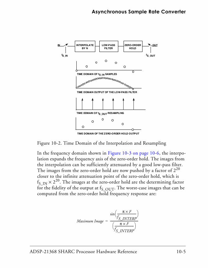
ADSP-21368 SHARC Processor Hardware Reference 10-5
Asynchronous Sample Rate Converter
In the frequency domain shown in Figure 10-3 on page 10-6, the interpo-lation expands the frequency axis of the zero-order hold. The images from the interpolation can be sufficiently attenuated by a good low-pass filter. The images from the zero-order hold are now pushed by a factor of 220 closer to the infinite attenuation point of the zero-order hold, which is fS_IN × 220. The images at the zero-order hold are the determining factor for the fidelity of the output at fS_OUT. The worst-case images that can be computed from the zero-order hold frequency response are:
Figure 10-2. Time Domain of the Interpolation and Resampling
IN OUT
fS_IN fS_OUT
TIME DOMAIN OF fS_IN SAMPLES
TIME DOMAIN OUTPUT OF THE LOW-PASS FILTER
TIME DOMAIN OF fS_OUT RESAMPLING
TIME DOMAIN OF THE ZERO-ORDER HOLD OUTPUT
INTERPOLATEBY N
LOW-PASSFILTER
ZERO-ORDERHOLD
Maximum Image
π F×fS_INTERP----------------------------⎝ ⎠⎛ ⎞sin
π F×fS_INTERP----------------------------⎝ ⎠⎛ ⎞
-----------------------------------------=

Theory of Operation
10-6 ADSP-21368 SHARC Processor Hardware Reference
F is the frequency of the worst-case image which is:
and fS_INTERP is
The following worst-case images would appear for fS_IN = 192 kHz:
Image at fS_INTERP – 96 kHz = –125.1 dB
Image at fS_INTERP + 96 kHz = –125.1 dB
Figure 10-3. Frequency Domain of the Interpolation and Resampling
220
fS_IN×fS_IN
2------------±
fS_IN 220×
FREQUENCY DOMAIN OF SAMPLES AT fS_IN
FREQUENCY DOMAIN OF THE INTERPOLATION
FREQUENCY DOMAIN OF fS_OUT RESAMPLING
FREQUENCY DOMAIN AFTERRESAMPLING
IN OUT
fS_IN fS_OUT
INTERPOLATEBY N
LOW-PASSFILTER
ZERO-ORDERHOLD
fS_IN
220 × fS_IN
220 × fS_IN
220 × fS_IN
SIN(X)/X OF ZERO-ORDER HOLD

ADSP-21368 SHARC Processor Hardware Reference 10-7
Asynchronous Sample Rate Converter
Hardware ModelThe output rate of the low-pass filter of Figure 10-2 is the interpolation rate, 220 × 192 kHz = 201.3 GHz. Sampling at a rate of 201.3 GHz is clearly impractical, not to mention the number of taps required to calcu-late each interpolated sample. However, since interpolation by 220 involves zero-stuffing 220– 1 samples between each fS_IN sample, most of the multiplies in the low-pass FIR filter are by zero. A further reduction can be realized by the fact that since only one interpolated sample is taken at the output at the fS_OUT rate, only one convolution needs to be per-formed per fS_OUT period instead of 220 convolutions. A 64-tap FIR filter for each fS_OUT sample is sufficient to suppress the images caused by the interpolation.
The difficulty with the above approach is that the correct interpolated sample needs to be selected upon the arrival of fS_OUT. Since there are 220 possible convolutions per fS_OUT period, the arrival of the fS_OUT clock must be measured with an accuracy of 1/201.3 GHz = 4.96 ps. Measuring the fS_OUT period with a clock of 201.3 GHz frequency is clearly impossi-ble; instead, several coarse measurements of the fS_OUT clock period are made and averaged over time.
Another difficulty with the above approach is the number of coefficients required. Since there are 220 possible convolutions with a 64-tap FIR fil-ter, there needs to be 220 polyphase coefficients for each tap, which requires a total of 226 coefficients. To reduce the amount of coefficients in ROM, the SRC stores a small subset of coefficients and performs a high-order interpolation between the stored coefficients. So far the above approach works for the case of fS_OUT > fS_IN. However, in the case when the output sample rate, fS_OUT, is less than the input sample rate, fS_IN, the ROM starting address, input data, and the length of the convolution must be scaled. As the input sample rate rises over the output sample rate, the anti-aliasing filter’s cutoff frequency has to be lowered because the Nyquist frequency of the output samples is less than the Nyquist fre-quency of the input samples. To move the cutoff frequency of the

Sample Rate Converter Architecture
10-8 ADSP-21368 SHARC Processor Hardware Reference
anti-aliasing filter, the coefficients are dynamically altered and the length of the convolution is increased by a factor of (fS_IN/fS_OUT). This tech-nique is supported by the Fourier transform property that if f(t) is F(ω), then f(k × t) is F(ω/k). Thus, the range of decimation is simply limited by the size of the RAM.
Sample Rate Converter ArchitectureFigure 10-4 shows a top level block diagram of the SRC module and Figure 10-5 shows architecture details. The sample rate converter’s FIFO block adjusts the left and right input samples and stores them for the FIR filter’s convolution cycle. The fS_IN counter provides the write address to the FIFO block and the ramp input to the digital-servo loop. The ROM stores the coefficients for the FIR filter convolution and performs a high-order interpolation between the stored coefficients. The sample rate ratio block measures the sample rate by dynamically altering the ROM coefficients and scaling the FIR filter length and input data. The digi-tal-servo loop automatically tracks the fS_IN and fS_OUT sample rates and provides the RAM and ROM start addresses for the start of the FIR filter convolution.
The master clock input (MCLK) shown in Figure 10-4 is peripheral clock (PCLK) divided by 4 (which is core clock divided by 8). There-fore, MCLK = PCLK ÷ 4 = CCLK ÷ 8

ADSP-21368 SHARC Processor Hardware Reference 10-9
Asynchronous Sample Rate Converter
The FIFO receives the left and right input data and adjusts the amplitude of the data for both the soft muting of the SRC and the scaling of the input data by the sample rate ratio before storing the samples in RAM. The input data is scaled by the sample rate ratio because as the FIR filter length of the convolution increases, so does the amplitude of the convolu-tion output. To keep the output of the FIR filter from saturating, the input data is scaled down by multiplying it by (fS_OUT/fS_IN) when fS_OUT < fS_IN. The FIFO also scales the input data to mute and stop muting the SRC.
The RAM in the FIFO is 512 words deep for both left and right channels. An offset to the write address, provided by the fS_IN counter, is added to prevent the RAM read pointer from overlapping the write address. The offset is selectable by the GRPDLYS (group delay select) signal. A small offset (16) is added to the write address pointer when GRPDLYS is high, and a large offset, (64), is added to the write address pointer when GRPDLYS is
Figure 10-4. Sample Rate Converter Block Diagram
SERIALINPUTPORT
LRCLK_I
SCLK_I
SDATA_I
SMODE_IN2-0
HARD_MUTE_IN
TDM_OUT
DE-EMPHASISFILTER
MUTE_OUT
DE-EMPHASIS1-0
SAMPLERATE
CONVERTER
MUTE_IN
SRC_RATIO14-0
SERIALOUTPUT
PORT
LRCLK_O
SCLK_O
SDATA_O
TDM_IN
SMODE_OUT1-0
WLENGTH_OUT1-0
21BIT_DITHER
MATCHED_PHASED_MODE
MCLK

Sample Rate Converter Architecture
10-10 ADSP-21368 SHARC Processor Hardware Reference
low. Increasing the offset of the write address pointer is useful for applica-tions when small changes in the sample rate ratio between fS_IN and fS_OUT are expected. The maximum decimation rate can be calculated from the RAM word depth and GRPDLYS as (512 – 16)/64 taps = 7.75 for short group delay and (512 – 64)/64 taps = 7 for long group delay.
The digital-servo loop is essentially a ramp filter that provides the initial pointer to the address in RAM and ROM for the start of the FIR convolu-tion. The RAM pointer is the integer output of the ramp filter while the ROM pointer is the fractional part. The digital-servo loop must be able to provide excellent rejection of jitter on the fS_IN and fS_OUT clocks as well as measure the arrival of the fS_OUT clock within 4.97 ps. The digi-tal-servo loop also divides the fractional part of the ramp output by the ratio of fS_IN/fS_OUT for the case when fS_IN > fS_OUT, to dynamically alter the ROM coefficients.
Figure 10-5. Sample Rate Converter Architecture
fS_INCOUNTER
FIFOHIGHROM A
DIGITALSERVO LOOP FIR FILTER
ROM B
ROM C
ROM D
ORDER
INTERP
SAMPLE RATERATIO
SAMPLE RATE RATIO L/R DATA OUT
EXTERNALRATIO
RIGHT DATA IN
LEFT DATA IN
fS_ IN
fS_OUT
ADSP-21368 SHARC Processor Hardware Reference 10-11
Asynchronous Sample Rate Converter
The digital-servo loop is implemented with a multi-rate filter. To settle the digital-servo loop filter quickly at startup or at a change in the sample rate, a fast mode has been added to the filter. When the digital-servo loop starts up or the sample rate is changed, the digital-servo loop kicks into fast mode to adjust and settle on the new sample rate. Upon sensing the digital-servo loop settling down to some reasonable value, the digital-servo loop kicks into normal or slow mode. During fast mode, the MUTE_OUT sig-nal of the SRC is asserted to remind the user to mute the SRC which avoids clicks and pops.
The FIR filter is a 64-tap filter in the case of fS_OUT < fS_IN and is (fS_IN/fS_OUT) × 64 taps for the case when fS_IN > fS_OUT. The FIR filter performs its convolution by loading in the starting address of the RAM address pointer and the ROM address pointer from the digital-servo loop at the start of the fS_OUT period. The FIR filter then steps through the RAM by decrementing its address by 1 for each tap, and the ROM pointer increments its address by the (fS_OUT/fS_IN) × 220 ratio for fS_IN > fS_OUT or 220 for fS_OUT < fS_IN. Once the ROM address rolls over, the convolution is complete. The convolution is performed for both the left and right channels, and the multiply/accumulate circuit used for the convolution is shared between the channels.
The fS_IN/fS_OUT sample rate ratio circuit is used to dynamically alter the coefficients in the ROM for the case when fS_IN > fS_OUT. The ratio is calculated by comparing the output of an fS_OUT counter to the output of an fS_IN counter. If fS_OUT > fS_IN, the ratio is held at one. If fS_IN >fS_OUT, the sample rate ratio is updated if it is different by more than two fS_OUT periods from the previous fS_OUT to fS_IN comparison. This is done to provide some hysteresis to prevent the filter length from oscillat-ing and causing distortion.
However, the hysteresis of the fS_OUT/fS_IN ratio circuit can cause phase mismatching between two SRCs operating with the same input and out-put clocks. Since the hysteresis requires a difference of more than two fS_OUT periods to update the fS_OUT/fS_IN ratio, two SRCs may have

SRC Operation
10-12 ADSP-21368 SHARC Processor Hardware Reference
differences in their ratios from 0 to 4 fS_OUT period counts. The fS_OUT/fS_IN ratio adjusts the filter length of the SRC, which corresponds directly with the group delay. Thus, the magnitude in the phase difference depends upon the resolution of the fS_OUT and fS_IN counters. The greater the resolution of the counters, the smaller the phase difference error.
Group DelayWhen multiple SRCs are used with the same serial input port clock and the same serial output port clock, the hysteresis causes different group delays between multiple SRCs. The filter group delay of the SRC is given by the equations:
SRC OperationThe following sections provide details on the SRC’s operation within the ADSP-21367/8/9 and ADSP-2137x processors.
The maximum data that is transferred through the SRCs is 24-bit. When 32-bit clock and data is provided to the 128 dB SRC, the least significant 8-bits are zero. However for a 140 dB SRC, the least significant 8-bits contain the ratio information. This informa-tion should be considered while interfacing the SRC to interfaces such as the S/PDIF.
GDS 16fS_IN-------------- 32
fS_IN-------------- onds for fS_OUT
fS_IN>sec+=
GDS 16fS_IN--------------
32fS_IN--------------⎝ ⎠⎛ ⎞
fS_INfS_OUT---------------------⎝ ⎠⎜ ⎟⎛ ⎞
× onds for fS_OUT fS_IN<sec+=

ADSP-21368 SHARC Processor Hardware Reference 10-13
Asynchronous Sample Rate Converter
Enabling the SRCWhen the SRCx_ENABLE bit (bit 31 in the SRC control registers) is set (= 1), the SRC begins its initialization routine where all locations in the FIFO are initialized to zero, MUTE_OUT is cleared, and any output pins are enabled.
The SRCx_ENABLE bit should be held low for a minimum of five PCLK cycles when setting or clearing the bit. It is recommended that the SRC be dis-abled when changing modes.
When the SRCx_ENABLE bit is set or there is a change in the sample rate between LRCLK_I and LRCLK_O, the MUTE_OUT pin is cleared. The MUTE_OUT pin remains cleared until the digital-servo loop’s internal fast settling mode is complete. When the digital-servo loop has switched to slow set-tling mode, the MUTE_OUT pin is set. While MUTE_OUT is cleared, the MUTE_IN pin should be cleared as well to prevent any major distortion in the audio output samples.
Serial Data PortsThe serial data ports provide the interface through which data is trans-ferred into and out of the SRC modules. The following sections describe the various data formats and the available modes of operation.
Data Format
The serial data input port mode is set by the logic levels on the SRCx_SMODEIN[0:2] bits that are located in the SRCCTLx registers. The serial data input port modes available are left-justified, I2S, TDM and right-justified, 16, 18, 20, or 24 bits as defined in Table 10-1.
The serial data output port mode is set by the logic levels on the SRCx_SMODE_OUT[0:1] bits. The serial mode can be changed to left-justi-fied, I2S, right-justified, or TDM as defined in Table 10-2. The output word width can be set by using the SRCx_LENOUT[0:1] bits as shown in
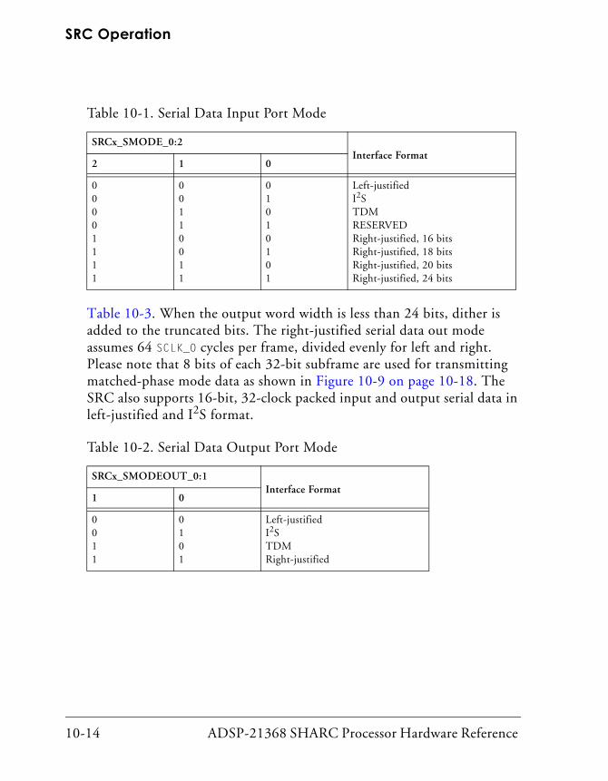
SRC Operation
10-14 ADSP-21368 SHARC Processor Hardware Reference
Table 10-3. When the output word width is less than 24 bits, dither is added to the truncated bits. The right-justified serial data out mode assumes 64 SCLK_O cycles per frame, divided evenly for left and right. Please note that 8 bits of each 32-bit subframe are used for transmitting matched-phase mode data as shown in Figure 10-9 on page 10-18. The SRC also supports 16-bit, 32-clock packed input and output serial data in left-justified and I2S format.
Table 10-1. Serial Data Input Port Mode
SRCx_SMODE_0:2Interface Format
2 1 0
00001111
00110011
01010101
Left-justifiedI2STDMRESERVEDRight-justified, 16 bitsRight-justified, 18 bitsRight-justified, 20 bitsRight-justified, 24 bits
Table 10-2. Serial Data Output Port Mode
SRCx_SMODEOUT_0:1Interface Format
1 0
0011
0101
Left-justifiedI2STDMRight-justified

ADSP-21368 SHARC Processor Hardware Reference 10-15
Asynchronous Sample Rate Converter
Time-Division Multiplex (TDM) Output Mode
In TDM output mode, several SRCs can be daisy-chained together and connected to the serial input port of an ADSP-21367/8/9 and ADSP-2137x processor or other processor (Figure 10-6). The SRC con-tains a 64-bit parallel load shift register. When the LRCLK_O pulse arrives, each SRC parallel loads its left and right data into the 64-bit shift register. The input to the shift register is connected to the TDM_IN signal, while the output is connected to the SDATA_O signal. By connecting the SDATA_O sig-nal to the TDM_IN signal of the next SRC, a large shift register is created, which is clocked by the SCLK_O signal.
The number of SRCs that can be daisy-chained together is limited by the maximum frequency of SCLK_O signals, which is about 25 MHz. For exam-ple, if the output sample rate, fS, is 48 kHz, up to eight SRCs could be connected since 512 × fS is less than 25 MHz.
Table 10-3. Word Width
SRCx_LENOUT_0:1Interface Format
1 0
0011
0101
24 bits20 bits18 bits16 bits
Figure 10-6. TDM Output Mode
SRCx
TDM_INSDATA_O
LRCLK_O
SCLK_O
ADSP-2136x
DR0
RFS0
RCLK0
SCLK
LRCLK
SRCx
TDM_INSDATA_O
LRCLK_O
SCLK_O
SRCx
TDM_INSDATA_O
LRCLK_O
SCLK_O

SRC Operation
10-16 ADSP-21368 SHARC Processor Hardware Reference
TDM Input Mode
In TDM input mode, several SRCs can be daisy-chained together and connected to the serial input port of an ADSP-21367/8/9 and ADSP-2137x processor or other processor (Figure 10-7). The SRC con-tains a 64-bit parallel load shift register. When the LRCLK_I pulse arrives, each SRC parallel loads its left and right data into the 64-bit shift register. The input to the shift register is connected to the SDATA_IN, while the output is connected to the TDM_I signal. By connecting the SDATA_I signal to the TDM_I signal of the next SRC, a large shift register is created, which is clocked by the SCLK_I signal.
The number of SRCs that can be daisy-chained together is limited by the maximum frequency of the SCLK_O signal, which is about 25 MHz. For example, if the output sample rate, fS, is 48 kHz, up to eight SRCs could be connected since 512 × fS is less than 25 MHz.
Matched-Phase Mode
The matched-phase mode is the mode discussed in “Theory of Operation” on page 10-2. This mode eliminates the phase mismatch between multiple SRCs. The master SRC device transmits its fS_OUT/fS_IN ratio through the SDATA_O pin to the slave SRC’s TDM_IN pins. The slave SRCs receive the transmitted fS_OUT/fS_IN ratio and use the transmitted fS_OUT/fS_IN ratio instead of their own internally-derived fS_OUT/fS_IN ratio as shown
Figure 10-7. TDM Input Mode
SRCx
SDATA_I
LRCLK_I
SCLK_I
ADSP-2136x
DR0
TFS0
TCLK0
SRCx
TDM_OUTSDATA_I
LRCLK_I
SCLK_I
SRCx
SDATA_I
LRCLK_I
SCLK_I
SCLK
LRCLK
TDM_OUT TDM_OUT

ADSP-21368 SHARC Processor Hardware Reference 10-17
Asynchronous Sample Rate Converter
in Figure 10-8. The master device can have both its serial ports in slave mode as depicted, or either one in master mode. The slave SRCs must have their MATASE_2 bits set to 1, respectively. The LRCLK_I and LRCLK_O signals may be asynchronous with respect to each other in this mode.
There must be 32 SCLK_O cycles per subframe in matched-phase mode. The SRC supports the matched-phase mode for all serial output data for-mats: left-justified, I2S, right-justified, and TDM mode.
Note that in the left-justified, I2S, and TDM modes, the lower eight bits of each channel subframe are used to transmit the matched-phase data. In right-justified mode, the upper eight bits are used to transmit the matched-phase data. This is shown in Figure 10-9.
Figure 10-8. Typical Configuration for Matched-Phase Mode Operation
SRCxSLAVE1
SDATA_O
SRCxPHASE-MASTER
SRCxSLAVE2
SRCXSLAVEn
LRCLKI (FS_IN)
SCLKI
LRCLKO(FS_OUT)
SCLKO(64FS_OUT)
RESET
SDOMSDO1SDO2
SDON
TDM_IN
SDATA_I
LRCLK_I
SCLK_I
RESET
SCLK_O
LRCLK_O
SDATA_O
TDM_IN
SDAT A_I
LRCLK_I
SCLK_I
RESET
SCLK_O
LRCLK_O
SDATA_O
TDM_IN
SDATA_I
LRCLK_I
SCLK_I
RESET
SCLK_O
LRCLK_O
SDATA_O
TDM_IN
SDATA_I
LRCLK_I
SCLK_I
RESET
SCLK_O
LRCLK_O

SRC Operation
10-18 ADSP-21368 SHARC Processor Hardware Reference
Bypass Mode
When the BYPASS bit is set (=1), the input data bypasses the sample rate converter and is sent directly to the serial output port. Dithering of the output data when the word length is set to less than 24 bits is disabled. This mode is ideal when the input and output sample rates are the same and the LRCLK_I and LRCLK_O signals are synchronous with respect to each other. This mode can also be used for passing through non-audio data since no processing is performed on the input data in this mode.
De-Emphasis FilterAs discussed, the serial input port generates a frame synchronization sig-nal, UN_fS_IN, that derives its clock from the positive edge of the PCLK signal. The UN_fS_IN signal asserts when a new frame of left and right data is available for the de-emphasis filter and the SRC. The de-emphasis filter is used to de-emphasize audio data that has been emphasized. The type of de-emphasis filter is selected by the SRCn_DEEMPHASIS1–0 bits and is based on the input sample rate as follows:
• 00 – No de-emphasis, audio data is passed directly to the SRC
• 01 – 32 kHz sample rate de-emphasis filter
Figure 10-9. Matched-Phase Data Transmission
AUDIO DATA RIGHTCHANNEL, 16 BITS - 24 BITS
MATCHED-PHASE
DATA, 8 BITS
MATCHED-PHASE
DATA, 8 BITS
AUDIO DATA LEFTCHANNEL, 16 BITS - 24 BITS
Left-Justified, I2S, and TDM Mode
Right-Justified Mode
AUDIO DATA LEFT CHANNEL, MATCHED-PHASE
DATA, 8 BITS
AUDIO DATA RIGHT
24 BITS CHANNEL, 24 BITSMATCHED-PHASE
DATA, 8 BITS

ADSP-21368 SHARC Processor Hardware Reference 10-19
Asynchronous Sample Rate Converter
• 10 – 44.1 kHz sample rate de-emphasis filter
• 11 – 48 kHz sample rate de-emphasis filter
After the audio data is passed from the de-emphasis filter to the SRC, the SRC converts the audio data from the input sample rate to the output sample rate. When the serial output port needs new data, the frame syn-chronization signal, (UN_fS_OUT), is asserted from the serial output port. Like the UN_fS_IN signal, the UN_fS_OUT signal derives its clock from the positive edge of the PCLK signal. The UN_fS_OUT and UN_fS_IN sig-nals are used by the SRC to perform the sample rate conversion. The SRCRAT register indicates the sample rate ratio of UN_fS_OUT/UN_fS_IN.
Mute ControlWhen the SRCx_ENABLE bit is enabled (set = 1), or when the sample rate between the input and output LRCLK changes, the SRC begins its initializa-tion routine and the MUTE_OUT signal is asserted. When MUTE_OUT is asserted, the MUTE_IN signal should also be asserted to avoid any unwanted output.
When the MUTE_IN pin is asserted high, the MUTE_IN control performs a soft mute by linearly decreasing the input data to the SRC FIFO to zero, (–144 dB attenuation). A 12-bit counter, clocked by the LRCLK_I signal, is used to control the mute attenuation. Therefore, the time it takes from the assertion of the MUTE_IN signal to –144 dB, (full mute attenuation) is 4096 LRCLK clock cycles. Likewise, the time it takes to reach 0 dB mute attenua-tion from the deassertion of the MUTE_IN signal is 4096 LRCLK cycles.
The mute feature of the SRC can be controlled automatically in hardware using the MUTE_IN signal by connecting it to the MUTE_OUT signal. By default, the two signals for each SRC are connected. Automatic muting can be disabled using the SRCx_MUTE_DIS bits in the SRCMUTE register.

SRC Operation
10-20 ADSP-21368 SHARC Processor Hardware Reference
Muting can also be controlled in software using the MUTE bits (SRCx_SOFTMUTE, SRCx_HARD_MUTE, SRCx_AUTO_MUTE) in the SRC control register (SRCCTL) as described below. For more information, see “SRC Registers” on page 10-21.
Soft Mute
When the SRCx_SOFTMUTE bit in the SRCCTL register is set, the MUTE_IN sig-nal is asserted, and the SRC performs a soft mute by linearly decreasing the input data to the SRC FIFO to zero, (–144 dB attenuation) as described for automatic hardware muting.
Hard Mute
When the SRCx_HARD_MUTE bit in the SRCCTL register is set, the SRC imme-diately mutes the input data to the SRC FIFO to zero, (–144 dB attenuation).
Auto Mute
When the SRCx_AUTO_MUTE bit in the SRCCTL register is set, the SRC com-municates with the SPDIF receiver peripheral to determine when the input should mute. Each SRC is connected to the NOAUDIO bits in the out-put of the SPDIF receiver (see “Receiver Status Register (DIRSTAT)” on page A-94). When this signal is asserted, the SRC immediately mutes the input data to the SRC FIFO to zero, (–144 dB attenuation). This mode is useful for automatic detection of non-PCM audio data received from the S/PDIF receiver.

ADSP-21368 SHARC Processor Hardware Reference 10-21
Asynchronous Sample Rate Converter
SRC RegistersThe SRC uses five 32-bit registers to configure and operate the SRC module.
• SRCCTL0, SRC control 0. This read/write register is used to con-trol the operating modes, filters, and data formats used in the SRC0 and SRC1 modules. This register is located at address 0x2490.
• SRCCTL1, SRC control 1. This read/write register is used to con-trol the operating modes, filters, and data formats used in the SRC2 and SRC3 modules. This register is located at address 0x2491.
• SRCMUTE, SRC mute. This read/write register performs mute-out to mute-in control and provides status information for the SRC3–0 modules. This register is located at address 0x2492.
• SRCRAT0, SRC output to input ratio 0. This read-only register reports the mute and I/O sample ratio for SRC0 and SRC1. This register is located at address 0x2498.
• SRCRAT1, SRC output to input ratio 1. This read-only register reports the mute and I/O sample ratio for SRC2 and SRC3. This register is located at address 0x2499.
For complete register bit descriptions, see “SRC Control Registers (SRC-CTLx)” on page A-97.

Programming the SRC Module
10-22 ADSP-21368 SHARC Processor Hardware Reference
Programming the SRC ModuleUse the following guidelines when developing programs that include the SRC module.
SRC Control Register ProgrammingInitially, programs configure the SRC control registers SRCCTL0 and SRCCTL1. The SRCCTL0 register contains control parameters for the SRC0 and SRC1 modules and the SRCCTL1 register contains control values for the SRC2 and SRC3 modules. The control parameters include mute information, data formats for input and output ports, de-emphasis enable, dither enable, and matched-phase mode enable for multiple SRCs. Write the settings to the desired control register at least one cycle before setting the corresponding SRC module enable bit, SRCx_ENABLE.
SRU ProgrammingThe SRU (signal routing unit) needs to be programmed in order to con-nect the SRCs to the output pins or any other peripherals.
For normal operation, the data, clock, and frame sync signals need to be routed as shown in Table 10-4.
Table 10-4. SRC Signal Routing
Signal Definition
SRCx_DAT_IP_I SRC module data input
SRCx_CLK_IP_I SRC module clock input
SRCx_FS_IP_I SRC module frame sync input
SRCx_DAT_OP_I SRC module data output
SRCx_CLK_OP_I SRC module clock output
SRCx_FS_OP_O SRC module frame sync output

ADSP-21368 SHARC Processor Hardware Reference 10-23
Asynchronous Sample Rate Converter
For information on using the SRU, see “Making Connections in the SRUs” on page 4-15, and “DAI/SRU1 Connection Groups” on page 4-18.
SRC Mute-Out InterruptOnce the SRC is locked (after 4K input samples), the corresponding SRCx_MUTE_OUT bit in the DAI_IRPTL_H/L register is set. This generates the DAI_INTH/L interrupt. From this point, the SRC produces output serial data at the output sampling frequency. The SRC mute signals can be used to generate interrupts on their leading edge, falling edge, or both, depend-ing on how the DAI_IRPT_RE/FE registers are programmed.
Sample Rate RatioOnce the SRC mute interrupt has triggered, the SRCRAT0 and SRCRAT1 reg-isters can be read to find the ratio of output to input sampling frequency. This ratio is reported in 4.11 (integer.fraction) format.
Programming SummarySince the SRC data is not available to the core, programming the SRC peripheral involves simply connecting the SRU to the on-chip (serial ports or input data port) or off-chip (DAI pins) serial devices. These devices provide the clock and data to be converted, and select the desired operat-ing mode in the SRC control register. This setup can be accomplished in two steps.
1. Connect each of the four SRCs to their two serial clocks (SRCx_CLK_IP_I, SRCx_CLK_OP_I) and frame sync inputs (SRCx_FS_IP_I, SRCx_FS_OP_I). Also connect one data input (SRCx_DAT_IP_I) and one data output (SRCx_DAT_OP_O) in the SRU.

Programming the SRC Module
10-24 ADSP-21368 SHARC Processor Hardware Reference
In multichannel, or matched-phase modes, the TDM signals must also be connected. (See Table 10-1 on page 10-14 and Table 10-2 on page 10-14.)
2. Initialize the SRCCTLx register to enable the SRCs.

ADSP-21368 SHARC Processor Hardware Reference 11-1
11 UART PORT CONTROLLER
The universal asynchronous receiver/transmitter (UART) is a full-duplex peripheral compatible with the PC-style, industry-standard UART. The UART converts data between serial and parallel formats. The serial format follows an asynchronous protocol that supports various word lengths, stop bits, and parity generation options. The UART includes interrupt han-dling hardware. Interrupts can be generated from 12 different events.
The ADSP-21367/8/9 and ADSP-2137x processors contain two UARTs which support multiprocessor communication using 9-bit address detec-tion. This allows the units to be used in multi-drop networks using the RS-485 data interface standard.
The two independent UARTs are referred to as UART0 and UART1. Both are identical and each has its own set of control and status registers. The content in this chapter applies to both UARTs unless otherwise specified.
The UART is a DMA-capable peripheral with support for separate trans-mit and receive DMA master channels. It can be used in either DMA or programmed non-DMA modes of operation. The non-DMA mode requires software management of the data flow using either interrupts or polling. The DMA method requires minimal software intervention as the DMA engine itself moves the data. For more information, see “UART DMA” on page 2-44.
Either one of the peripheral timers can be used to provide a hard-ware-assisted autobaud detection mechanism for use with the UART. See the ADSP-2136x SHARC Processor Programming Reference, “Timers” chap-ter for more information.

Serial Communications
11-2 ADSP-21368 SHARC Processor Hardware Reference
Serial CommunicationsThe UART follows an asynchronous serial communication protocol with these options:
• 5 – 8 data bits
• 1 or 2 stop bits
• None, even, or odd parity
• Baud rate = PCLK/(16 × divisor), where PCLK is the system clock fre-quency and the divisor can be a value from 1 to 65,536
All data words require a start bit and at least one stop bit. With the optional parity bit, this creates a 7- to 12-bit range for each word. The for-mat of received and transmitted character frames is controlled by the line control register (UARTxLCR). Data is always transmitted and received least significant bit (LSB) first.
Figure 11-1 shows a typical physical bit stream measured on the transmit pin.
Figure 11-1. Bit Stream on the Transmit Pin
DATA BITS STOP BIT(S)
START BIT LSB PARITY BIT (OPTIONAL, ODD OR EVEN)
D0 D1 D2 D3 D4 D5 D6 D7

ADSP-21368 SHARC Processor Hardware Reference 11-3
UART Port Controller
UART Control and Status RegistersThe processor provides a set of PC-style, industry-standard control and status registers for each UART. These memory-mapped registers (MMRs) are byte-wide registers that are mapped as half-words with the most signif-icant byte zero-filled.
Consistent with industry-standard interfaces, multiple registers are mapped to the same address location. The transmit holding, divisor latch low, and receive buffer registers share an address and the interrupt enable and divisor latch high registers share an address. The divisor latch access bit (UARTDLAB, bit 7) in the line control register (UARTxLCR) controls which set of registers is accessible at a given time.
Transmit and receive channels are both buffered. The UARTxTHR register buffers the transmit shift register (UARTxTSR) and the UARTxRBR register buffers the receive shift register (UARTxRSR). The shift registers are not directly accessible by software.
These registers are also shown and described in “UART Control and Sta-tus Registers” on page A-118.
UARTxLCR RegistersThe UART line control register (UARTxLCR) controls the format of received and transmitted character frames. The UARTSB bit (bit 6) functions even when the UART clock is disabled. Since the transmit pin normally drives high, it can be used as a flag output pin when the UART is not used. The parity and word length select controls are not valid in 9-bit mode. In 9-bit mode, the word length is always 8 and the 9th bit is transmitted instead of the parity bit.

UART Control and Status Registers
11-4 ADSP-21368 SHARC Processor Hardware Reference
UARTxLSR RegisterThe UART line status register (UARTxLSR) contains UART status informa-tion as shown in Figure A-49 on page A-120.
The break interrupt (UARTBI), overrun error (UARTOE), parity error (UARTPE), and framing error (UARTFE) bits are cleared when the UART line status register (UARTxLSR) is read. The data ready (UARTDR) bit is cleared when the UART receive buffer register (UARTxRBR) is read.
Because of the destructive nature of reading these registers, shadow registers are provided for reading the contents of the corresponding main registers. The shadow registers, UARTxIIRSH, return exactly the same contents as the main register, but without changing the register’s status in any way. These registers are 32-bit registers located at address 0x3C0A (for UATR0LSRSH) and 0x400A (for UART1LSRSH).
The UARTTHRE bit (bit 6) indicates that the UART transmit channel is ready for new data, and software can write to the UARTxTHR register. Writes to UARTxTHR clear the UARTTHRE bit. It is set again when data is copied from UARTxTHR to the transmit shift register (UARTxTSR). The UARTTEMT bit can be evaluated to determine whether a recently initiated transmit operation has been completed.
UARTxTHR RegisterA write to the UART transmit holding register (UARTxTHR) initiates the transmit operation. The data is moved to the internal transmit shift regis-ter (UARTxTSR) where it is shifted out at a baud rate equal to PCLK/(16 × Divisor) with start, stop, and parity bits appended as required. All data words begin with a 1-to-0 transition start bit. The transfer of data from the UARTxTHR register to the transmit shift register sets the transmit holding register empty status flag (UARTTHRE) in the UART line status reg-ister (UARTxLSR).

ADSP-21368 SHARC Processor Hardware Reference 11-5
UART Port Controller
This 32-bit write only register uses only 18-bits. The other bits are filled with zeros during writes. In no-pack mode (default), only the lower byte is used—all other bits are zero filled. However in pack mode, both the high and low bytes are used (Figure 11-2). The TX9Dx bits are the ninth bit in 9-bit transmission mode. This register is mapped to the same address as the UARTxRBR and UARTxDLL registers. A write to the UART transmit hold-ing register (UARTxTHR) initiates the transmit operation.
To access the UARTxTHR register, the UARTDLAB bit in the UARTxLCR register must be cleared. When the UARTDLAB bit is cleared, writes to this address target the UARTxTHR register, and reads from this address return the UAR-TxRBR register.
Note that data is transmitted and received by the least significant bit (LSB) first (bit 0) followed by the most significant bits (MSBs).
UARTxRBR RegisterThe receive operation uses the same data format as the transmit configura-tion, except that the number of stop bits is always assumed to be 1. After detection of the start bit, the received word is shifted into the receive shift register (UARTxRSR) at a baud rate of PCLK/(16 x Divisor). After the appro-priate number of bits (including stop bit) is received, the data and any status are updated and the UARTxRSR register is transferred to the UART receive buffer register (UARTxRBR), shown in Figure 11-3 and Figure A-51 on page A-122. After the transfer of the received word to the UARTxRBR buffer and the appropriate synchronization delay, the data ready status flag (UARTDR) is updated.
Figure 11-2. Transmit Holding Register (Packing Enabled)
31 0781524 23
TX9D0
9
TX9D1 ZERO-FILLED LOWER BYTEHIGHER BYTEZERO-FILLED

UART Control and Status Registers
11-6 ADSP-21368 SHARC Processor Hardware Reference
A sampling clock equal to 16 times the baud rate samples the data as close to the midpoint of the bit as possible. Because the internal sample clock may not exactly match the asynchronous receive data rate, the sampling point drifts from the center of each bit. The sampling point is synchro-nized again with each start bit, so the error accumulates only over the length of a single word. A receive filter removes spurious pulses of less than two times the sampling clock period.
The 32-bit, read-only UARTxRBR register is mapped to the same address as the write-only UARTxTHR and UARTxDLL registers. In no pack mode (default), only the lower byte is used—all other bits are zero-filled. How-ever in pack mode, both the high and low bytes are used. The RX9Dx bits are the 9th bit in 9-bit transmission mode. To access UARTxRBR, the UARTD-LAB bit in the UARTxLCR register must be cleared. When the UARTDLAB bit is cleared, writes to this address target the UARTxTHR register, while reads from this address return the UARTxRBR register.
Because of the destructive nature of reading these registers, shadow registers are provided for reading the contents of the corresponding main registers. The shadow registers, UARTxRBRSH, return exactly the same contents as the main register, but without changing the status in any way. These registers are 32-bit registers located at address 0x3C08 (for UART0RBRSH) and 0x4008 (for UART1RBRSH).
Figure 11-3. Receive Buffer Register (Packing Enabled)
31 0781524 23
RX9D0
9
RX9D1 ZERO-FILLED LOWER BYTEHIGHER BYTEZERO-FILLED

ADSP-21368 SHARC Processor Hardware Reference 11-7
UART Port Controller
UARTxIER RegisterThe UART interrupt enable registers (UARTxIER) are used to enable requests for system handling of empty or full states of UART data regis-ters. Unless polling is used as a means of action, the UARTRBFIE and/or UARTTBEIE bits in this register are normally set.
Setting these registers without enabling system DMA causes the UART to notify the processor of the state of the data inventory by means of inter-rupts. For proper operation in this mode, system interrupts must be enabled, and appropriate interrupt handling routines must be present. For backward compatibility, the UARTxIIR registers still reflect the correct interrupt status.
With system DMA enabled, the UART uses DMA to transfer data to or from the processor. Dedicated DMA channels are available to receive and transmit operations. Line error handling can be configured completely independently from the receive/transmit setup.
The UARTxIER register is mapped to the same address as the UARTxDLH reg-ister. To access the UARTxIER register, the UARTDLAB bit in the UARTxLCR register must be cleared.
The UART interrupts are all combined into the digital peripheral inter-face (DPI) interrupt. The DPI_IRPTL register determines whether an interrupt is for the transmitter or receiver. For DMA, the transmit inter-rupt is generated when a DMA in transmit mode is complete whereas the receive interrupt is generated when receive DMA is complete or when a receive error occurs. The UARTxRXSTAT register reports whether the inter-rupt is due to DMA completion or errors.
The UART receive and transmit interrupt can also be programmed through the peripheral interrupt control registers (PICR) as separate inter-rupts for DMA. (By default, these interrupts are not configured in the IRPTL register—the PICR register has to be programmed to configure them.) For I/O mode, both the transmit and receive interrupt can be

UART Control and Status Registers
11-8 ADSP-21368 SHARC Processor Hardware Reference
programmed through the PICR register using the code select value for the UART receive interrupt (0x13 for UART0 interrupt and 0x14 for UART1 receive interrupt). Similar to I/O mode, both the transmit and receive interrupts are mapped to the receive interrupt. Then the UARTxIER register can be used to select the transmit or receive interrupt respectively for I/O mode. The following examples show two methods of enabling transmit DMA in I/O mode. The first method uses the DPI interrupt directly.
Listing 11-1. Enabling Transmit DMA (DPI Direct Method)
bit set mode1 IRPTEN; /* enables global interrupts */
bit set imask DPII; /* unmasks DPI interrupt */
ustat1 = UART0_RX_INT;
dm(DPI_IRPTL_RE) = ustat1; /* enables transmit interrupt in
I/O mode */
The second method uses the DPI interrupt by programming the PICR with the code value of the UART0 receive interrupt (0x13).
Listing 11-2. Enabling Transmit DMA (DPI PICR Method)
#define MASKP14 (0x1f<<10)
#define UART0Rx (0x13<<10)
bit set mode1 IRPTEN;
/* Map the UART0 receive interrupt to P14 using the programmable
interrupt controller */
ustat1 = dm(PICR2);
bit clr ustat1 MASKP14;
bit set ustat1 UART0Rx;
dm(PICR2) = ustat1;
bit set IMASK P14I; /* Unmasks the UART Receive interrupt */

ADSP-21368 SHARC Processor Hardware Reference 11-9
UART Port Controller
For information on using the UART for DMA transfers, see “UART DMA” on page 2-44, “DAI/DPI Interrupt Controller” on page 4-65, and “Peripheral Interrupt Priority Control Registers” on page A-164.
Even though the UART has two interrupts for receive and trans-mit, in I/O mode, all interrupts are grouped as a single receive interrupt.
The UARTLSIE bit (bit 2) enables interrupt generation on an independent interrupt channel when any of the following conditions are raised by the respective bit in the UART line status register (UARTxLSR):
• Receive overrun error (UARTOE)
• Receive parity error (UARTPE)
• Receive framing error (UARTFE)
• Break interrupt (UARTBI)
When the UARTTBEIE bit is set in the UARTxIER register in I/O mode, the UART module immediately issues an interrupt. When initiating the trans-mission of a string, no special handling of the first character is required. Set the UARTTBEIE bit (bit 1) and let the interrupt service routine (ISR) load the first character from memory and write it to the UARTxTHR register in the normal manner. Accordingly, the UARTTBEIE bit should be cleared if the string transmission has completed.
UARTxIIR RegisterFor legacy reasons, the UART interrupt identification register (UARTxIIR) still reflects the UART interrupt status (see Table 11-1). Legacy operation may require bundling all UART interrupt sources to a single interrupt channel and servicing them all by the same software routine. This can be established by globally assigning all UART interrupts to the same

UART Control and Status Registers
11-10 ADSP-21368 SHARC Processor Hardware Reference
interrupt priority using the peripheral interrupt priority control registers. For more information, see “Peripheral Interrupt Priority Control Regis-ters” on page A-164.
When cleared, the pending interrupt bit (NINT) signals that an interrupt is pending. The STATUS field indicates the highest priority pending inter-rupt. The receive line status has the highest priority; the UARTTXFI interrupt has the lowest priority. In the case where both interrupts are sig-nalling, the UARTxIIR register reads 0x06.
When a UART interrupt is pending, the interrupt service routine (ISR) needs to clear the interrupt latch explicitly. For information on how to clear the latches see “Interrupt Identification Registers (UARTxIIR)” on page A-124.
The transmit interrupt request is cleared by writing new data to the UAR-TxTHR register or by reading the UARTxIIR register. Please note the special role of the UARTxIIR register read in the case where the service routine does not want to transmit further data.
Table 11-1. IIR Register in I/O Mode
Bit Status NINT Interrupt Priority
Interrupt Type Cleared When...
000 1 – No interrupt –
011 0 1 Rx line status LSR is read
100 0 2 Address detect RBR is read
010 0 3 Rx data ready RBR is read
001 0 4 THR empty Write THR or Read IIR when priority = 4
000 0 5 THR and TSR empty Write THR or Read IIR when priority = 5

ADSP-21368 SHARC Processor Hardware Reference 11-11
UART Port Controller
If software stops transmission, it must read the UARTxIIR register to reset the interrupt request. As long as the UARTxIIR register reads 0x04 or 0x06 (indicating that another interrupt of higher priority is pending), the UAR-TxTHR empty latch cannot be cleared by reading the UARTxIIR register.
The following restrictions should be noted.
1. If either the line status interrupt or the receive data interrupt has been assigned a lower interrupt priority by the interrupt controller, a deadlock condition can occur. To avoid this, always assign the lowest priority of the enabled UART interrupts to the UARTxTHR empty event.
2. Because of the destructive nature of reading these registers, shadow registers are provided for reading the contents of the corresponding main registers. The shadow registers, UARTxIIRSH, return exactly the same contents as the main register, but without changing the status in any way. These registers are 32-bit registers located at address 0x3C09 (for UART0IIRSH) and 0x4009 (for UART1IIRSH).
UARTxDLL and UARTxDLH RegistersThe bit rate is characterized by the peripheral clock (PCLK = 2 x CCLK) and the 16-bit divisor. The divisor is split into the UART divisor latch low byte register (UARTxDLL) and the UART divisor latch high byte register (UARTxDLH). These registers form a 16-bit divisor. The baud clock is divided by 16 so that:
Divisor = 1 when UARTxDLL = UARTxDLH = 1
Divisor = 65,535 when UARTxDLL = UARTxDLH = FF
The UARTxDLL register is mapped to the same address as the UARTxTHR and UARTxRBR registers. The UARTxDLH register is mapped to the same address as the interrupt enable register (UARTxIER). The DLAB bit in the UARTxLCR reg-ister must be set before the UART divisor latch registers can be accessed.

UART Control and Status Registers
11-12 ADSP-21368 SHARC Processor Hardware Reference
The 16-bit divisor formed by the UARTxDLH and UARTxDLL registers resets to 0x0001, resulting in the highest possible clock frequency by default. If the UART is not used, disabling the UART clock saves power (see bits 13 and 14 in the “Power Management Con-trol Register (PMCTL)” on page A-170). The UARTxDLH and UARTxDLL registers can be programmed by software before or after turning on the clock.
Table 11-2 provides example divide factors required to support most stan-dard baud rates.
Careful selection of PCLK frequencies, that is, even multiples of desired baud rates, can result in lower error percentages.
UARTxSCR RegisterThe contents of the 8-bit UART scratch register (UARTxSCR) is reset to 0x00. It is used for general-purpose data storage and does not control the UART hardware in any way.
Table 11-2. UART Baud Rate Examples With 100 MHz PCLK
Baud Rate DL Actual % Error
2400 2604 2400.15 0.006
4800 1302 4800.31 0.007
9600 651 9600.61 0.006
19200 326 19,171.78 0.147
38400 163 38,343.56 0.147
57600 109 57,339.45 0.452
115200 54 115,740.74 0.469
921,600 7 892,857.14 3.119
6,250,000 1 6,250,000 –

ADSP-21368 SHARC Processor Hardware Reference 11-13
UART Port Controller
For information on UART DMA registers, see “UART DMA” on page 2-44.
UARTxMODE RegisterThe UART mode register controls miscellaneous settings such as packing and address detection. For more information, see “Mode Registers (UAR-TxMODE)” on page A-126.
I/O ModeIn I/O mode, data is moved to and from the UART by the processor core. To transmit a character, load it into the UARTxTHR register. Received data can be read from the UARTxRBR register. The processor must write and read one character at time.
To prevent any loss of data and misalignments of the serial data stream, the UART line status register (UARTxLSR) provides two status flags for handshaking—UARTTHRE and UARTDR.
The UARTTHRE flag is set when the UARTxTHR register is ready for new data and cleared when the processor loads new data into the UARTxTHR register. Writing this register when it is not empty overwrites the register with the new value and the previous character is never transmitted.
The UARTDR flag signals when new data is available in the UARTxRBR regis-ter. This flag is cleared automatically when the processor reads from this register. Reading the UARTxRBR register when it is not full returns the pre-viously received value. When the UARTxRBR register is not read in time, newly received data overwrites the UARTxRBR register and the overrun (UAR-TOE) flag is set.
With interrupts disabled, these status flags can be polled to determine when data is ready to move. Note that because polling is processor-inten-sive, it is not typically used in real-time signal processing environments.

I/O Mode
11-14 ADSP-21368 SHARC Processor Hardware Reference
Software can write up to two words into the UARTxTHR register before enabling the UART clock. As soon as the UART DMA engine is enabled, those two words are sent.
Alternatively, UART writes and reads can be accomplished by interrupt service routines (ISRs). Separate interrupt lines are provided for the trans-mit, receive, and error signals. The independent interrupts can be enabled individually by the UARTxIER register. In I/O mode, the receive interrupt is generated for the following cases.
• When UARTxRBR is full
• On a receive overrun error
• On a receive parity error
• On a receive framing error
• On a break interrupt (RXSIN held low)
• When UARTxTHR is empty
• A transmit complete (UARTTXFI) interrupt
• An address detect (UARTADI) interrupt (for 9-bit mode)
The ISRs can evaluate the status bit field within the UART interrupt iden-tification register (UARTxIIR) to determine the signalling interrupt source. If more than one source is signalling, the status field displays the one with the highest priority. Interrupts also must be assigned and unmasked by the processor’s interrupt controller. The ISRs must clear the interrupt latches explicitly. See Figure A-54 on page A-125 and “Interrupt Priorities” on page B-4.

ADSP-21368 SHARC Processor Hardware Reference 11-15
UART Port Controller
Packing ModeThe UART provides packed and unpacked modes of data transfer to and from the internal memory of the ADSP-21367/8/9 and ADSP-2137x pro-cessors. This mode is set using the UARTPACK bit (bit 0) in the UARTxMODE register. In unpacked mode, the data word is appended to the left with 24 zeros during transmission or reception. In packed mode, two words of data are transmitted or received with their corresponding higher bytes filled with zeros. For example, consecutive data words 0xAB and 0xCD are packed as 0x00CD 00AB in the receiver, and 0x00CD 00AB is trans-mitted as two words of 0xAB and 0xCD successively from the transmitter. The packed feature is provided to use the internal memory of the proces-sor in a more efficient manner. Packing is available in both I/O and DMA modes. A control bit, UARTPKSYN, can be used to re synchronize the pack-ing. For information on using the UART for DMA transfers, see “UART DMA” on page 2-44.
Note that in packed mode, both the transmitter and receiver operate with an even number of words. A transmit-buffer-empty or receive-buffer-full interrupt is generated only after an even number of words are transferred. In 9-bit mode, the address detect interrupt can be generated whenever the receiver gets an address word, irrespective of the packing mode. This helps programs respond to an address word immediately. The program is expected to take into account these features when using packed mode.
Programs must use care when using the packing feature in 9-bit mode.
Programs should write the UARTPKSYN bit (bit 1) with a 1 each time an address is received. This starts the reception of the following data from the lower half-word of the UARTxRBR register.
The address-detect interrupt is generated whenever the UART receiver receives an address, irrespective of the packing. The DR bit in the UARTxLSR register can be used to discover whether the address is in the lower (DR = 0) or higher half-word (DR = 1).

Packing Mode
11-16 ADSP-21368 SHARC Processor Hardware Reference
The LSR register must be read before reading the UARTxRBR register, because the latter clears the DR bit. Reading the UARTxRBR register clears both the address-detect and the data-ready interrupts. In non-packed mode, when the address-detect interrupt is generated, it means that the data is ready in the RBR buffer while in packed mode, this is not the case.

ADSP-21368 SHARC Processor Hardware Reference 12-1
12 TWO WIRE INTERFACE CONTROLLER
The two wire interface (TWI) controller allows a device to interface to an inter-IC bus as specified by the Philips I2C Bus Specification version 2.1 dated January 2000.
OverviewThe TWI is fully compatible with the widely used I2C bus standard. It was designed with a high level of functionality and is compatible with multimaster, multislave bus configurations. To preserve processor band-width, the TWI controller can be set up and a transfer initiated with interrupts only. This allows the processor to service FIFO buffer data reads and writes. Protocol-related interrupts are optional.
The TWI moves 8-bit data externally while maintaining compliance with the I2C bus protocol. The TWI controller includes the following features.
• Simultaneous master and slave operation on multiple device systems
• Support for multimaster data arbitration
• 7-bit addressing
• 100K bits/second and 400K bits/second data rates
• General call address support
• Master clock synchronization and support for clock low extension

Architecture
12-2 ADSP-21368 SHARC Processor Hardware Reference
• Separate multiple-byte receive and transmit FIFOs
• Low interrupt rate
• Individual override control of data and clock lines in the event of a bus lockup
• Input filter for spike suppression
Table 12-1 shows the pins for the TWI. Two bidirectional pins externally interface the TWI controller to the I2C bus. The interface is simple and no other external connections or logic are required.
ArchitectureFigure 12-1 illustrates the overall architecture of the TWI controller.
The peripheral interface supports the transfer of 32-bit wide data and is used by the processor in the support of register and FIFO buffer reads and writes.
The register block contains all control and status bits and reflects what can be written or read as outlined by the programmer’s model. Status bits can be updated by their respective functional blocks.
The FIFO buffer is configured as a 1-byte-wide, 2-deep transmit FIFO buffer and a 1-byte-wide, 2-deep receive FIFO buffer.
Table 12-1. TWI Pins
Pin Description
SDA In/Out TWI serial data, high impedance reset value
SCL In/Out TWI serial clock, high impedance reset value

ADSP-21368 SHARC Processor Hardware Reference 12-3
Two Wire Interface Controller
The transmit shift register serially shifts its data out externally off chip. The output can be controlled to generate acknowledgements or it can be manually overwritten.
The receive shift register receives its data serially from off chip. The receive shift register is 1 byte wide and data received can either be trans-ferred to the FIFO buffer or used in an address comparison.
The address compare block supports address comparison in the event the TWI controller module is accessed as a slave.
The prescaler block must be programmed to generate a 10 MHz time ref-erence relative to the peripheral clock. This time base is used for filtering data and timing events specified by the electrical parameters in the data sheet (see the I2C bus specification from Philips), as well as for SCL clock generation.
Figure 12-1. TWI Block Diagram
IRQ
SDA
REGISTERS
PERIPHERALINTERFACE
CLOCK GENERATION
PRESCALER
ADDRESS COMPARE
RECEIVE SHIFTREGISTER
ARBITRATION
SCL
TRANSMIT SHIFTREGISTER
FIFO

Register Descriptions
12-4 ADSP-21368 SHARC Processor Hardware Reference
The clock generation module is used to generate an external serial clock (SCL) when in master mode. It includes the logic necessary for synchroni-zation in a multimaster clock configuration and clock stretching when configured in slave mode.
Register DescriptionsThe TWI controller has 16 registers which are described in the following sections. More information on these registers can be found in “Two Wire Interface Registers” on page A-130.
TWI Master Internal Time RegisterThe TWI control register (TWIMITR) is used to enable the TWI module as well as to establish a relationship between the peripheral clock (PCLK) and the TWI controller’s internally-timed events. The internal time reference is derived from PCLK using a prescaled value.
PRESCALE = fPCLK/10 MHz
Additional information for the TWIMITR register bits includes:
TWI Enable (TWIEN). This bit must be set for slave or master mode opera-tion. It is recommended that this bit be set and remain set at the time PRESCALE is initialized. This guarantees accurate operation of bus busy detection logic.
Prescale (PRESCALE). This value should be set to the number of peripheral clock periods that equals the time period corresponding to a 10 MHz fre-quency. This number is represented as a 7-bit binary value.

ADSP-21368 SHARC Processor Hardware Reference 12-5
Two Wire Interface Controller
TWIDIV RegisterDuring master mode operation, the serial clock divider register (TWIDIV) values are used to create the high and low durations of the serial clock (SCL). Serial clock frequencies can vary from 400 kHz to less than 20 kHz. The resolution of the generated clock is 1/10 MHz or 100 ns.
CLKDIV = TWI SCL period ÷ 10 MHz time reference
For example, for an SCL of 400 kHz (period = 1/400 kHz = 2500 ns) and an internal time reference of 10 MHz (period = 100 ns):
CLKDIV = 2500 ns ÷ 100 ns = 25
For an SCL with a 30% duty cycle, then CLKLOW = 17 and CLKHI = 8.
Note that CLKLOW and CLKHI add up to CLKDIV.
Additional information for the TWIDIV register bits can be found in “Clock Divider Register (TWIDIV)” on page A-132.
Slave Mode Control RegisterThe TWI slave mode control register (TWISCTL) controls the logic associ-ated with slave mode operation. Settings in this register do not affect master mode operation and should not be modified to control master mode functionality.
Additional information for the TWISCTL register bits can be found in “Slave Mode Control Register (TWISCTL)” on page A-133.

Register Descriptions
12-6 ADSP-21368 SHARC Processor Hardware Reference
Slave Mode Address RegisterThe TWI slave mode address register (TWISADDR) holds the slave mode address, which is the valid address that the slave-enabled TWI controller responds to. The TWI controller compares this value with the received address during the addressing phase of a transfer. For more information, see “Slave Address Register (TWISADDR)” on page A-135.
Slave Mode Status RegisterDuring and at the conclusion of slave mode transfers, the TWI slave mode status register (TWISSTAT) holds information on the current transfer. Gen-erally, slave mode status bits are not associated with the generation of interrupts. Master mode operation does not affect slave mode status bits. For more information, see “Slave Status Register (TWISSTAT)” on page A-135.
Master Mode Control RegisterThe TWI master mode control register (TWIMCTL) controls the logic associ-ated with master mode operation. Bits in this register do not affect slave mode operation and should not be modified to control slave mode func-tionality. For more information, see “Master Control Register (TWIMCTL)” on page A-136.
Master Mode Address RegisterDuring the addressing phase of a transfer, the TWI controller, with its master enabled, transmits the contents of the TWI master mode address register (TWIMADDR). When programming this register, omit the read/write bit. That is, only the upper 7 bits that make up the slave address should be written to this register. For example, if the slave address is 1010000, then the TWI_MASTER_ADDR register is programmed with 1010000, which corre-sponds to 0x50. When sending out the address on the bus, the TWI

ADSP-21368 SHARC Processor Hardware Reference 12-7
Two Wire Interface Controller
controller appends the read/write bit as appropriate based on the state of the MDIR bit in the master mode control register. For more information, see “Master Address Register (TWIMADDR)” on page A-139.
Master Mode Status RegisterThe TWI master mode status register (TWIMSTAT) holds information dur-ing master mode transfers and at their conclusion. Generally, master mode status bits are not directly associated with the generation of interrupts but offer information on the current transfer. Slave mode operation does not affect master mode status bits. This is a read-only register. For more infor-mation, see “Master Status Register (TWIMSTAT)” on page A-140.
FIFO Control RegisterThe TWI FIFO control register (TWIFIFOCTL) affect only the FIFO and is not tied in any way with master or slave mode operation. For more infor-mation, see “FIFO Control Register (TWIFIFOCTL)” on page A-143.
FIFO Status RegisterThe fields in the TWI FIFO status register (TWIFIFOSTAT) indicate the state of the FIFO buffers’ receive and transmit contents. The FIFO buffers do not discriminate between master data and slave data. By using the sta-tus and control bits provided, the FIFO can be managed to allow simultaneous master and slave operation. All bits in this register are read-only. For more information, see “FIFO Status Register (TWIFIFOS-TAT)” on page A-145.
Interrupt Source RegisterThe TWI interrupt source register (TWIIRPTL) contains information about functional areas requiring servicing. Many of the bits in this register serve as an indicator to further read and service various status registers.

Register Descriptions
12-8 ADSP-21368 SHARC Processor Hardware Reference
After servicing the interrupt source associated with a bit, programs must clear that interrupt source bit. All bits are sticky and W1C-type. For more information, see “Interrupt Source Register (TWIIRPTL)” on page A-147.
Interrupt Enable RegisterThe TWI interrupt enable register (TWIIMASK) allows interrupt sources to assert the interrupt output. Each enable bit corresponds with one inter-rupt source bit in the TWI interrupt source register (TWIIRPTL). Reading and writing the TWI interrupt enable register does not affect the contents of the TWI interrupt source register. For all bits, 0 = interrupt generation disabled and 1 = interrupt generation enabled. For more information, see “Interrupt Enable Register (TWIIMASK)” on page A-150.
8-Bit Transmit FIFO RegisterThe TWI 8-bit transmit FIFO register (TXTWI8) holds an 8-bit data value written into the FIFO buffer. Transmit data is entered into the corre-sponding transmit buffer in a first-in, first-out order. Although peripheral bus writes are 32 bits, a write access to the TXTWI8 register adds only one transmit data byte to the FIFO buffer. With each access, the transmit sta-tus (TWITXS) field in the TWIFIFOSTAT register is updated. If an access is performed while the FIFO buffer is full, the core waits until there is at least one byte space in the transmit FIFO buffer and then completes the write access. The bits in this register are write-only. For more information, see “8-Bit Transmit FIFO Register (TXTWI8)” on page A-152.
16-Bit Transmit FIFO RegisterThe TWI 16-bit FIFO transmit register (TXTWI16) holds a 16-bit data value written into the FIFO buffer. Although peripheral bus writes are 32 bits, a write access to the TXTWI16 register adds only two transmit data bytes to the FIFO buffer. To reduce interrupt output rates and peripheral

ADSP-21368 SHARC Processor Hardware Reference 12-9
Two Wire Interface Controller
bus access times, a double byte transfer data access can be performed. Two data bytes can be written, effectively filling the transmit FIFO buffer with a single access.
The data is written in little-endian byte order as shown in Figure 12-2, where byte 0 is the first byte to be transferred and byte 1 is the second byte to be transferred. With each access, the transmit status (TWITXS) field in the TWIFIFOSTAT register is updated. If an access is performed while the FIFO buffer is not empty, the core waits until the FIFO buffer is com-pletely empty and then completes the write access. All bits in this register are write-only. This register always reads as 0x00000000. For more infor-mation, see “16-Bit Transmit FIFO Register (TXTWI16)” on page A-153.
8-Bit Receive FIFO RegisterThe TWI 8-bit FIFO receive register (RXTWI8) holds an 8-bit data value read from the FIFO buffer. Receive data is read from the corresponding receive buffer in a first-in, first-out order. Although peripheral bus reads are 32 bits, a read access to the RXTWI8 register can only access one receive data byte from the FIFO buffer. With each access, the receive status (TWIRXS) field in the TWIFIFOSTAT register is updated. If an access is per-formed while the FIFO buffer is empty, the core waits until there is at least one byte in the receive FIFO buffer and then completes the read access. All bits in this register are read-only. For more information, see “8-Bit Receive FIFO Register (RXTWI8)” on page A-154.
Figure 12-2. Little-Endian Byte Order
B1 B0
DATA IN REGISTER
07816 15232431
UNUSEDUNUSED

Data Transfer Mechanics
12-10 ADSP-21368 SHARC Processor Hardware Reference
16-Bit Receive FIFO RegisterThe TWI 16- bit FIFO receive register (RXTWI16) holds a 16-bit data value read from the FIFO buffer. Although peripheral bus reads are 32 bits, a read access to the RXTWI16 register can only access two receive data bytes from the FIFO buffer. To reduce interrupt output rates and peripheral bus access times, a double-byte receive data access can be performed. Two data bytes can be read, effectively emptying the receive FIFO buffer with a single access.
The data is read in little-endian byte order, as shown in Figure 12-2 on page 12-9, where byte 0 is the first byte received and byte 1 is the second byte received. With each access, the receive status (TWIRXS) field in the TWIFIFOSTAT register is updated to indicate it is empty. If an access is per-formed while the FIFO buffer is not full, the core waits until the receive FIFO buffer is full and then completes the read access. All bits in this reg-ister are write-only. For more information, see “16-Bit Receive FIFO Register (RXTWI16)” on page A-154.
Data Transfer MechanicsThe TWI controller follows the transfer protocol of the Philips I2C Bus Specification version 2.1 dated January 2000. A simple complete transfer is diagrammed in Figure 12-3.
Figure 12-3. Basic Data Transfer
7-BIT ADDRESS 8-BIT DATAR/W ACK PACKS
S = START
P = STOP
ACK = ACKNOWLEDGE

ADSP-21368 SHARC Processor Hardware Reference 12-11
Two Wire Interface Controller
To better understand the mapping of TWI controller register contents to a basic transfer, Figure 12-4 details the same transfer as above noting the corresponding TWI controller bit names. In this illustration, the TWI controller successfully transmits one byte of data. The slave has acknowl-edged both address and data.
Clock Generation and SynchronizationThe TWI controller only issues a clock during master mode operation and only at the time a transfer has been initiated. If arbitration for the bus is lost, the serial clock output immediately three-states. If multiple clocks attempt to drive the serial clock line, the TWI controller synchronizes its clock with the other remaining clocks. This is illustrated in Figure 12-5.
The TWI controller’s serial clock (SCL) output follows these rules:
• Once the clock high (CLKHI) count is complete, the serial clock out-put is driven low and the clock low (CLKLOW) count begins.
• Once the clock low count is complete, the serial clock line is three-stated and the clock synchronization logic enters into a delay mode (shaded area) until the SCL line is detected at a logic 1 level. At this time, the clock high count begins.
Figure 12-4. Data Transfer With Bit Illustration
MADDR[6:0] MDIR ACK PACKS
S = START
P = STOP
ACK = ACKNOWLEDGE
TWI_XMT_BYTE

Data Transfer Mechanics
12-12 ADSP-21368 SHARC Processor Hardware Reference
Bus ArbitrationThe TWI controller initiates a master mode transmission (TWIMEN) only when the bus is idle. If the bus is idle and two masters initiate a transfer, arbitration for the bus begins. This is illustrated in Figure 12-6.
The TWI controller monitors the serial data bus (SDA) while SCL is high. If SDA is determined to be an active logic 0 level while the internal TWI controller’s data is a logic 1 level, the TWI controller has lost arbitration and ends generation of clock and data. Note that arbitration is performed not only at serial clock edges, but also during the entire time SCL is high.
Start and Stop ConditionsStart and stop conditions involve serial data transitions while the serial clock is at logic 1 level. The TWI controller generates and recognizes these transitions. Typically, start and stop conditions occur at the beginning and at the conclusion of a transmission, with the exception of repeated start “combined” transfers, as shown in Figure 12-7.
Figure 12-5. TWI Clock Synchronization
HIGHCOUNT
LOWCOUNT
TWI CONTROLLERCLOCK
SECOND MASTERCLOCK
SCLRESULT

ADSP-21368 SHARC Processor Hardware Reference 12-13
Two Wire Interface Controller
The TWI controller’s special-case start and stop conditions include:
• TWI controller addressed as a slave-receiver
If the master asserts a stop condition during the data phase of a transfer, the TWI controller concludes the transfer (TWISCOMP).
Figure 12-6. TWI Bus Arbitration
Figure 12-7. TWI Start and Stop Conditions
START
SCL (BUS)
TWI CONTROLLERDATA
SECOND MASTERDATA
SDA (BUS)ARBITRATIONLOST
START
SCL (BUS)
SDA (BUS)
STOP

Data Transfer Mechanics
12-14 ADSP-21368 SHARC Processor Hardware Reference
• TWI controller addressed as a slave-transmitter
If the master asserts a stop condition during the data phase of a transfer, the TWI controller concludes the transfer (TWISCOMP) and indicates a slave transfer error (TWISERR).
• TWI controller as a master-transmitter or master-receiver
If the stop bit is set during an active master transfer, the TWI con-troller issues a stop condition as soon as possible to avoid any error conditions (as if data transfer count had been reached).
General Call SupportThe TWI controller always decodes and acknowledges a general call address if it is enabled as a slave (TWISEN) and if general call is enabled (TWIGC). General call addressing (0x00) is indicated by the setting of the GCALL bit, and by the nature of the transfer, the TWI controller is a slave-receiver. If the data associated with the transfer is to be not acknowl-edged (NAKed), the TWINAK bit can be set.
If the TWI controller is to issue a general call as a master-transmitter, the appropriate address and transfer direction can be set along with loading transmit FIFO data.
Fast ModeFast mode essentially uses the same mechanics as standard mode. It is the electrical specifications and timing that are different. When fast mode is enabled (TWIFAST), the following timings are modified to meet the electri-cal requirements.
• Serial data rise times before arbitration evaluation (tr)
• Stop condition setup time from serial clock to serial data (tSUSTO)
• Bus free time between a stop and start condition (tBUF)

ADSP-21368 SHARC Processor Hardware Reference 12-15
Two Wire Interface Controller
Programming ExamplesThe following sections include programming examples for general setup, slave mode, and master mode, as well as guidance for repeated start condi-tions. For an example of programming the TWI using the digital peripheral interface and SRU2, see “Configuring the Two Wire Interface” on page 4-73.
General SetupGeneral setup refers to register writes that are required for both slave mode and master mode operation. General setup should be performed before either the master or slave enable bits are set.
Programs should enable the TWI controller through the TWIMITR register and set the prescale value. Program the prescale value to the binary repre-sentation of fPCLK/10 MHz.
All values should be rounded up to the next whole number. The TWIEN enable bit must be set. Note that once the TWI controller is enabled, a bus busy condition may be detected.
Slave ModeWhen enabled, slave mode supports both receive and transmit data trans-fers. It is not possible to enable only one data transfer direction and not acknowledge (NAK) the other. This is reflected in the following setup.
1. Program the TWISADDR register. The appropriate 7 bits are used in determining a match during the address phase of the transfer in case of 7-bit addressing.

Programming Examples
12-16 ADSP-21368 SHARC Processor Hardware Reference
2. Program the TXTWI8 or TXTWI16 register. These are the initial data values to be transmitted in the event the slave is addressed as a transmitter. This is an optional step. If no data is written and the slave is addressed and a transmit is required, the serial clock (SCL) is stretched and an interrupt is generated.
3. Program the TWIFIFOCTL register. Indicate if transmit (or receive) FIFO buffer interrupts should occur with each byte transmitted (received) or with each 2 bytes transmitted (received).
4. Program the TWIIMASK register. Enable bits associated with the desired interrupt sources. As an example, programming the value 0x000F results in an interrupt output to the processor when a valid address match is detected, a valid slave transfer completes, a slave transfer has an error, or a subsequent transfer has begun but the previous transfer has not been serviced.
5. Program the TWISCTL register. This prepares and enables slave mode operation. As an example, programming the value 0x0005 enables slave mode operation, requires 7-bit addressing, and indi-cates that data in the transmit FIFO buffer is intended for slave mode transmission.
Table 12-2 shows what the interaction between the TWI controller and the processor might look like when the slave is addressed as a receiver.
Table 12-2. Slave Mode Setup Interaction (Slave Addressed as Receiver)
TWI Controller Master Processor
Interrupt: TWISINIT – Slave transfer has been initiated.
Acknowledge: Clear interrupt source bits.
Interrupt: TWIRXS – Receive buffer has 1 or 2 bytes (according to TWIRXINT).
Read receive FIFO buffer.Acknowledge: Clear interrupt source bits.
... ...
Interrupt: TWISCOMP – Slave transfer com-plete.
Read receive FIFO buffer.Acknowledge: Clear interrupt source bits.

ADSP-21368 SHARC Processor Hardware Reference 12-17
Two Wire Interface Controller
Master Mode Clock SetupMaster mode operation is set up and executed on a per-transfer basis. An example of programming steps for a receive and for a transmit are given separately in following sections. The clock setup programming step listed here is common to both transfer types.
Program the TWIDIV register. This defines the clock high duration and clock low duration.
Master Mode TransmitFollow these programming steps for a single master mode transmit:
1. Program the TWIMADDR register. This defines the address transmit-ted during the address phase of the transfer.
2. Program the TXTWI8 or TXTWI16 registers. This is the initial data transmitted. It is considered an error to complete the address phase of the transfer and not have data available in the transmit FIFO buffer.
3. Program the TWIFIFOCTL register. Indicate if transmit FIFO buffer interrupts should occur with each byte transmitted (8 bits) or with each 2 bytes transmitted (16 bits).
4. Program the TWIIMASK register. Enable bits associated with the desired interrupt sources. As an example, programming the value 0x0030 results in an interrupt output to the processor in the event that the master transfer completes, or if the master transfer has an error.

Programming Examples
12-18 ADSP-21368 SHARC Processor Hardware Reference
5. Program the TWIMCTL register. This prepares and enables master mode operation. As an example, programming the value 0x0201 enables master mode operation, generates a 7-bit address, sets the direction to master-transmit, uses standard mode timing, and transmits 8 data bytes before generating a stop condition.
Table 12-3 shows what the interaction between the TWI controller and the processor might look like using this example.
Master Mode ReceiveFollow these programming steps for a single master mode transmit:
1. Program the TWIMADDR register. This defines the address transmit-ted during the address phase of the transfer.
2. Program the TWIFIFOCTL register. Indicate if receive FIFO buffer interrupts should occur with each byte received (8 bits) or with each 2 bytes received (16 bits).
3. Program the TWIIMASK register. Enable bits associated with the desired interrupt sources. For example, programming the value 0x0030 results in an interrupt output to the processor in the event that the master transfer completes, and the master transfer has an error.
Table 12-3. Master Mode Transmit Setup Interaction
TWI Controller Master Processor
Interrupt: TWITXINT – Transmit buffer has 1 or 2 bytes empty (according to XMTINTLEN).
Write transmit FIFO buffer.Acknowledge: Clear interrupt source bits.
... ...
Interrupt: TWIMCOMP – Master transfer com-plete.
Acknowledge: Clear interrupt source bits.

ADSP-21368 SHARC Processor Hardware Reference 12-19
Two Wire Interface Controller
4. Program the TWIMCTL register. Ultimately this prepares and enables master mode operation. As an example, programming the value 0x0201 enables master mode operation, generates a 7-bit address, sets the direction to master-receive, uses standard mode timing, and receives 8 data bytes before generating a stop condition.
Table 12-4 shows what the interaction between the TWI controller and the processor might look like using this example.
Repeated Start ConditionIn general, a repeated start condition is the absence of a stop condition between two transfers initiated by the same master. The two transfers can be of any direction type. Examples include a transmit followed by a receive, or a receive followed by a transmit. During a repeated start trans-fer, each interrupt must be serviced correctly to avoid errors. The following sections are intended to assist the programmer with service rou-tine development.
Transmit/Receive Repeated Start Sequence
Figure 12-8 illustrates a repeated start data transmit followed by a data receive sequence.
Table 12-4. Master Mode Receive Setup Interaction
TWI Controller Master Processor
Interrupt: TWIRXINT – Receive buffer has 1 or 2 bytes (according to RCVINTLEN).
Read receive FIFO buffer.Acknowledge: Clear interrupt source bits.
... ...
Interrupt: TWIMCOMP – Master transfer complete.
Read receive FIFO buffer.Acknowledge: Clear interrupt source bits.

Programming Examples
12-20 ADSP-21368 SHARC Processor Hardware Reference
The tasks performed at each interrupt are:
• TWITXINT interrupt
This interrupt is generated every time the transmit FIFO has one or two byte locations available to be written. To service this inter-rupt, write a byte or word into the transmit FIFO registers (TXTWI8 or TXTWI16). During one of these interrupts (preferably the first time), do the following:
• Set the RSTART bit (or earlier when TWIMCTL register is pro-grammed first).
• Set the TWIMDIR bit to indicate the next transfer direction is receive. This should be done before the addressing phase of the next transfer begins.
• TWIMCOMP interrupt
This interrupt is generated because all data has been transferred (DCNT = 0). If no errors were generated, a start condition is initi-ated. At this time, program the following bits of TWI_MASTER_CTRL register:
• Clear RSTART (if this is the last transfer).
Figure 12-8. Transmit/Receive Data Repeated Start
7-BIT ADDRESS 7-BIT ADDRESSS ACK 8-BIT DATA 8-BIT DATAACK ACKS PACK
TWITXINT INTERRUPT
START
TWIMCOM INTERRUPTTWIMCOM INTERRUPT
TWIRXINT INTERRUPT
REPEATED START STOP
Shaded region indicates slave to master transmission.

ADSP-21368 SHARC Processor Hardware Reference 12-21
Two Wire Interface Controller
• Re-program DCNT with the desired number of bytes to receive.
• TWISERR interrupt
This interrupt is generated due to the arrival of a byte into the receive FIFO. Simple data handling is all that is required.
Receive/Transmit Repeated Start Sequence
Figure 12-9 illustrates a repeated start data receive followed by a data transmit sequence. The shading in the figure indicates the slave has the bus.
The tasks performed at each interrupt are:
• TWIRXINT interrupt
This interrupt is generated due to the arrival of one or two data bytes into the receive FIFO. The TWIRSTART bit should be set at this time (or earlier) and MDIR should be cleared to reflect the change in direction of the next transfer. The TWIMDIR bit must be cleared before the addressing phase of the subsequent transfer begins.
Figure 12-9. Receive/Transmit Data Repeated Start
7-BIT ADDRESS 7-BIT ADDRESSS ACK 8-BIT DATA 8-BIT DATANACK ACKS PACK
TWIRXINT INTERRUPT
START
TWIMCOM INTERRUPTTWIMCOM INTERRUPT
TWITXINT INTERRUPT
REPEATED START STOP
SHADING INDICATESSLAVE HAS THE BUS

Electrical Specifications
12-22 ADSP-21368 SHARC Processor Hardware Reference
• TWIMCOMP interrupt
This interrupt has occurred due to the completion of the data receive transfer. At this time the data transmit transfer begins. The TWIDCNT field should be set to reflect the number of bytes to be transmitted. Clear the TWIRSTART bit if this is the last transfer.
• TWITXINT interrupt
This interrupt is generated when there is one or two bytes of empty space in the FIFO. Simple data handling is all that is required.
• TWIMCOM interrupt
The transfer is complete.
Electrical SpecificationsAll logic complies with the electrical specification outlined in the Philips I2C Bus Specification version 2.1 dated January, 2000.

ADSP-21368 SHARC Processor Hardware Reference 13-1
13 PRECISION CLOCK GENERATORS
The precision clock generators (PCG) consist of four units, each of which generates a pair of signals (clock and frame sync) derived from a clock input signal. The units, A B, C, and D, are identical in functionality and operate independently of each other. The two signals generated by each unit are normally used as a serial bit clock/frame sync pair.
Note the definitions of various clock periods that are a function of CLKIN and the appropriate ratio control (Table 13-1).
The unit that generates the bit clock is relatively simple, since digital clock signals are usually regular and symmetrical. The unit that generates the frame sync output, however, is designed to be extremely flexible and capa-ble of generating a wide variety of framing signals needed by many types of peripherals that can be connected to the signal routing unit (SRU1). For more information, see “Signal Routing Units” on page 4-8.
Table 13-1. Clock Periods
Timing Requirements Description
tCK CLKIN clock period
tCCLK Processor core clock period
tPCLK Peripheral clock period = 2 × tCCLK

13-2 ADSP-21368 SHARC Processor Hardware Reference
The core phase-locked loop (PLL) has been designed to provide clocking for the processor core. Although the performance specifications of this PLL are appropriate for the core, they have not been optimized or speci-fied for precision data converters where jitter directly translates into time quantization errors and distortion.
As shown in Figure 13-1, the PCGs can accept clock inputs either directly from the external oscillator (or discrete crystal) connected to the CLKIN pin, from the peripheral clock (PCLK), or from any of the 20 DAI pins. This allows a design to contain an external clock with performance specifi-cations appropriate for the application target.
Note that clock and frame sync signals generated by the serial ports are also subject to these jitter problems because the SPORT clock is generated from the core clock. However, a SPORT can produce data output while
Figure 13-1. Clock Inputs
EXTERNALOSCILLATOR
COREPLL
SHARC ADSP-213xx
PRECISIONCLOCK
GENERATORS(A-D)
M/NCORE CLOCKGENERATOR
SERIALPORT
SIGNALROUTING
UNIT
CORECORE CLOCKBUFFER
AMP
SCLK
FSYNC
INPUT0
INPUT1 FS
YN
C
PC
LK
SC
LK

ADSP-21368 SHARC Processor Hardware Reference 13-3
Precision Clock Generators
being a clock and frame sync slave. The clock generated by the SPORT is sufficient for most of the serial communications, but it is suboptimal for analog/digital conversion. Therefore, all precision data converters should be synchronized to a clock generated by the PCG or to a clean (low jitter) clock that is fed into SRU1 off-chip through a pin.
Any clock or frame sync unit should be disabled (have its enable bit cleared) before changing any of the associated parameters.
Clock OutputsEach of the four units (A, B, C, and D) produces a clock output and a frame sync output. The clock output is derived from the input to the PCG with a 20-bit divisor as shown in the following equation.
If the divisor is zero or one, the PCG’s clock generation unit is bypassed, and the clock input is connected directly to the clock output. Otherwise, the PCG unit clock output frequency is equal to the input clock fre-quency, divided by a 20-bit integer. This integer is specified in bits 19–0 of the PCG_CTLx1 registers for units A, B, C and D respectively. These reg-isters and bits are also described in Table A-63 on page A-156 and Table A-64 on page A-157.
The clock outputs have four other control bits that enable the A, B, C, and D units, ENCLKA, ENCLKB, ENCLKC, and ENCLKD respectively (bits 31 of the PCG_CTLx0 registers). These bits enable (= 1) and disable (= 0) the clock output signal for units A, B, C, and D respectively. When disabled, clock output is held at logic low.
Frequency of Clock Output = Frequency of Clock Input
Clock Divisor

Frame Sync Outputs
13-4 ADSP-21368 SHARC Processor Hardware Reference
The CLKASOURCE bit (bit 31 in the PCG_CTLA1 registers) specifies the input source for the clock of the respective units (A, B, C, and D). When this bit is cleared (= 0), the input is sourced from the external oscillator, as shown in Figure 13-1. When set (= 1), the input is sourced from SRU1, as speci-fied in the PCG_EXTA_I bits in the SRU_CLK4 register. The CLKASOURCE bit is overridden if CLKA_SOURCE_IOP bit (bit 2) in the PCG_SYNC register is set. If the CLKA_SOURCE_IOP bit is set, the input is sourced from the peripheral clock. See “Group A Connections—Clock Signals” on page 4-19.
The PCG units B, C, and D function identically, except that the PCG_CTLB1, PCG_CTLC1, and PCG_CTLD1 bits (bit 31) indicate that the exter-nal source for these units is specified in PCG_EXTB_I, PCG_EXTC_I, and PCG_EXTD_I bits in the SRU_CLK4 and SRU_CLK5 registers. See Figure 4-16 on page 4-22 and Figure 4-17 on page 4-23.
Note that the clock output is always set (as closely as possible) to a 50% duty cycle. If the clock divisor is even, the duty cycle of the clock output is exactly 50%. If the clock divisor is odd, then the duty cycle is slightly less than 50%. The low period of the output clock is one input clock period more than the high period of the output clock. For higher values of an odd divisor, the duty cycle is close to 50%.
A PCG clock output cannot be fed to its own input. Setting SRU_CLK4[4:0] = 0x1C connects PCG_EXTA_I to logic low, not PCG_CLKA_O. Setting SRU_CLK4[9:5] = 0x1D connects PCG_EXTB_I to logic low, not PCG_CLKB_O.
Frame Sync OutputsEach of the four units (A through D) also produces a synchronization sig-nal for framing serial data. The frame sync outputs are much more flexible since they need to accommodate the wide variety of serial protocols used by peripherals.

ADSP-21368 SHARC Processor Hardware Reference 13-5
Precision Clock Generators
Frame sync generation from a unit is independently enabled and con-trolled. Sources for the frame sync generation can be either from the crystal buffer output, PCLK, or an external pin source. There is only one external source pin for both frame sync and clock output for a unit. If an external source is selected for both frame sync and clock output for a unit, then they operate on the same input signal. Apart from enable and source select control bits, frame sync generation is controlled by a 20-bit divisor, a 16-bit pulse width control, and a 20-bit phase control.
There are two modes of operation for the PCG frame sync. The divisor field determines if the frame sync operates in normal mode (divisor > 1) or bypass mode (divisor = 0 or 1).
Normal ModeIn normal mode, the frequency of the frame sync output is determined by the divisor where:
The high period of the frame sync output is controlled by the value of the pulse width control. The value of the pulse width control should be less than the value of the divisor.
The phase of the frame sync output is determined by the value of the phase control. If the phase is zero, then the positive edges of the clock and frame sync coincide, provided the divisors of the clock and frame sync are the same, the source for the clock and frame sync is also the same, and if clock and frame sync are enabled at the same time using a single instruction.
The number of input clock cycles that have already elapsed before the frame sync is enabled is equal to the difference between the divisor and the phase values. If the phase is a small fraction of the divisor, then the frame
Frequency of Clock Input Frame Sync Divisor
Frequency of Frame Sync Output = ( )

Frame Sync Outputs
13-6 ADSP-21368 SHARC Processor Hardware Reference
sync appears to lead the clock. If the phase is only slightly less than the divisor, then the frame sync appears to lag the clock. The frame sync phase should not be greater than the divisor.
Bypass ModeIn bypass mode, the frame sync divisor is either 0 or 1. There are two ways the bypass mode operates, depending on the STROBEA, STROBEB, STROBEC and STROBED bits of the PCG_PW and PCG_PW2 registers of the pulse width control register (PCG_PWx, see Table A-66 on page A-159). This is shown below.
• Direct bypass. If the STROBEA/B/C/D of the pulse width control reg-ister (PCG_PW, PCG_PW2) is reset to 0, then the input is directly passed to the frame sync output, either not inverted or inverted, depending on the INVFSA, INVFSB, INVFSC and INVFSD bits of the PCG_PW and PCG_PW2 registers.
• One-shot. In the bypass mode, if the least significant bit (LSB) of the PCG_PW register is set to 1, then a one-shot pulse is generated. This one-shot-pulse has a duration equal to the period of MISCA2_I for unit A, MISCA3_I for unit B, MISCA4_I for unit C, and MISCA5_I for unit D (see “Group E Connections—Interrupts and Miscella-neous Signals” on page 4-43). This pulse is generated either at the rising or at the falling edge of the input clock, depending on the value of the INVFSA, INVFSB, INVFSC, and INVFSD bits of the PCG_PW and PCG_PW2 registers.

ADSP-21368 SHARC Processor Hardware Reference 13-7
Precision Clock Generators
Frame Sync Output Synchronization With an External Clock
The frame sync output may be synchronized with an external clock by programming the PCG_SYNC and PCG_SYNC2 registers (shown in Figure A-77 on page A-160) and the PCG control registers (PCG_CTLA0–1, PCG_CTLB0–1, PCG_CTLC0–1, and PCG_CTLD0–1) appropriately. In this mode, the rising edge of the external clock is aligned with that of the frame sync output (shown in Figure 13-2). The external clock is routed to the PCG block from any of the SRU1 group A source signals through the SRU_CLK4 and SRU_CLK5 registers (described in Table 4-4 on page 4-23).
The synchronization with the external clock is enabled by setting bits 0 and 16 of the PCG_SYNC register for frame sync A or B and the PCG_SYNC2 register for C or D output. The phase must be programmed to 3, so that the rising edge of the external clock is in sync with the frame sync.
Programming should occur in the following order.
1. Program the PCG_SYNC and PCG_SYNC2 and the PCG_CTLA0–1, PCG_CTLB0–1, PCG_CTLC0–1, and PCG_CTLD0–1 registers appropriately.
2. Enable clock or frame sync, or both.
Since the rising edge of the external clock is used to synchronize with the frame sync, the frame sync output is not generated until a rising edge of the external clock is sensed.
The clock output cannot be aligned with the rising edge of the external clock as there is no phase programmability. Once CLKA through CLKD have been enabled (by programming bit 1 and bit 17 of the PCG_SYNC register for CLKA and CLKB respectively and, bit 1 and 17 of PCG_SYNC2 register for CLKC and CLKD respectively) these outputs are activated when a low-to-high transition is sensed in the external clock (MISCA4_I, MISCA5_I).

Frame Sync Output Synchronization With an External Clock
13-8 ADSP-21368 SHARC Processor Hardware Reference
Frame SyncFor a given frame sync, the output is determined by the following:
• Divisor. A 20-bit divisor of the input clock that determines the period of the frame sync. When set to 0 or 1, the frame sync oper-ates in bypass mode, otherwise it operates in normal mode.
• Phase. A 20-bit value that determines the phase relationship between the clock output and the frame sync output. Settings for phase can be anywhere between 0 to DIV – 1.
• Pulse width. A 16-bit value that determines the width of the fram-ing pulse. Settings for pulse width can be 0 to DIV – 1. If the pulse width is equal to 0 or the frame sync is even, then the actual pulse width of the output frame sync is:
For odd divisors the actual pulse width of the output frame sync is:
Figure 13-2. Clock Output Synchronization With External Clock
FSA OUTPUT
MCLK
EXT CLK
Pulse WidthFrameSyncDivisor
2----------------------------------------------=
Pulse WidthFrameSyncDivisor 1–
2-------------------------------------------------------=

ADSP-21368 SHARC Processor Hardware Reference 13-9
Precision Clock Generators
The frequency of the frame sync output is determined by:
When the divisor is set to any value other than 0 or 1, the processors oper-ate in normal mode.
The frame sync divisors (FSxDIV bits) are specified in bits 19–0 of the cor-responding PCG control registers (PCG_CTLx0). The pulse width of the frame sync output is equal to the number of input clock periods specified in the 16-bit field of the corresponding PCG pulse width register (PCG_PW for A and B, PCG_PW2 for C and D). Bits 15–0 specify the pulse width of frame sync A and C, and bits 31–16 specify the pulse width of frame sync B and D.
Phase ShiftPhase shift is a frame sync parameter that defines the phase shift of the frame sync with respect to the clock of the same unit. This feature allows shifting of the frame sync signal in time relative to clock signals. Frame sync phase shifting is often required by peripherals that need a frame sync signal to lead or lag a clock signal.
The amount of phase shifting is specified as a 20-bit value in the FSAPHASE_HI bit field (bits 29–20) of the appropriate PCG_CTLAO register and in the FSAPHASE_LO bit field (bits 29–20) of the PCG_CTLA1 register for unit A. A single 20-bit value spans these two bit fields. The upper half of the word (bits 19–10) resides in the PCG_CTLAO register, and the lower half (bits 9–0) resides in the PCG_CTLA1 register.
Similarly, the phase shift for frame syncs B, C, and D is specified in the corresponding PCG_CTLxO and PCG_CTLx1 registers.
Frequency of Clock InputFrame Sync Divisor

Phase Shift
13-10 ADSP-21368 SHARC Processor Hardware Reference
When using a clock and frame sync as a synchronous pair, the units must be enabled in a single atomic instruction before their parame-ters are modified. Both units must also be disabled in a single atomic instruction.
Phase Shift SettingsThe phase shift between clock and frame sync outputs may be pro-grammed under these conditions:
• The input clock source for the clock generator output and the frame sync generator output is the same.
• Clock and frame sync are enabled at the same time using a single atomic instruction.
• Frame sync divisor is an integral multiple of the clock divisor.
If the phase shift is 0, the clock and frame sync outputs rise at the same time. If the phase shift is 1, the frame sync output transitions one input clock period ahead of the clock transition. If the phase shift is divisor – 1, the frame sync transitions divisor – 1 input clock periods ahead of the clock transitions. This translates to the one input clock period after the clock transition (Figure 13-3).
Phase shifting is represented as a full 20-bit value so that even when frame sync is divided by the maximum amount, the phase can be shifted to the full range, from zero to one input clock short of the period.
Pulse WidthPulse width is the number of input clock periods for which the frame sync output is high. Pulse width should be less than the divisor of the frame sync. The pulse width of frame sync A is specified in the PWFSA bits (15–0) of the PCG_PW register and the pulse width of frame sync B is specified in the PWFSB bits (31–16) of the PCG_PW register. Similarly, the pulse width of

ADSP-21368 SHARC Processor Hardware Reference 13-11
Precision Clock Generators
frame sync C is specified in the PWFSC bits (15–0) of the PCG_PW2 register and the pulse width of frame sync D is specified in the PWFSD bits (31–16) of the PCG_PW2 register.
If the pulse width is equal to 0 or if the divisor is even, then the actual pulse width of the frame sync output is equal to:
If the pulse width is equal to 0 or if the divisor is odd, then the actual pulse width of the frame sync output is equal to:
Figure 13-3. Phase Shift Settings
FRAME SYNC OUTPUT(PHASE SHIFT = PERIOD -1)
CLOCK INPUT(FOR BOTH CLOCKAND FRAME SYNC)
ENABLE
FRAME SYNC OUT PUT(PHASE SHIFT = 0)
FRAME SYNC OUT PUT(PHASE SHIFT = 1)
CLOCK OUTPUT
FRAME SYNC OUT PUT(PHASE SHIFT = 2)
OTHER VALUES:CLOCK DIVISOR = 4F RAME SYNC DIVISOR = 16PULSE WIDTH = 8
Pulse WidthFrameSyncDivisor
2----------------------------------------------=
Pulse WidthFrameSyncDivisor 1–
2-------------------------------------------------------=

Phase Shift
13-12 ADSP-21368 SHARC Processor Hardware Reference
Bypass ModeWhen the divisor for the frame sync has a value of 0 or 1, the frame sync is in bypass mode, and the PCG_PW and PCG_PW2 registers have different func-tionality than in normal mode. Two bit fields determine the operation in this mode. The one-shot (which is a strobe pulse) frame sync A, B, C, or D (STROBEx) bit (bits 0 and 16 in the PCG_PW and PCG_PW2 registers, respec-tively) determines if the frame sync has the same width as the input, or of a single strobe. The active low frame sync select for the frame syncs (INVFSx) bit (bits 1 and 17 of the PCG_PW and PCG_PW2 registers respec-tively) determines the nature of the output in the simple bypass and single strobe modes as described below. For additional information about the PCG_PWx registers, see Figure A-76 on page A-159.
In bypass mode, bits 15–2 and bits 31–18 of the PCG_PWx registers are ignored.
Bypass as a Pass Through
When the STROBEx bit in the PCG_PWx register equals 0, the unit is bypassed and the output equals the input. If, for example, INVFSA (bit 1) for unit A or INVFSB (bit 17) for unit B is set, then the signal is inverted (see Figure 13-4).
Figure 13-4. Frame Sync Bypass
CLOCK INPUTFOR FRAME SYNC
FRAME SYNC OUTPUT(INVFSA = 0, STROBEA = 0)
FRAME SYNC OUTPUT(INVFSA = 1, STROBEA = 0)

ADSP-21368 SHARC Processor Hardware Reference 13-13
Precision Clock Generators
Bypass mode also enables the generation of a strobe pulse (one-shot). Strobe usage ignores the counter and looks to SRU1 to provide the input signal.
Bypass as a One-Shot
When the STROBEA or STROBEB bits (bit 0, bit 16 of the PCG_PW register) or STROBEC or STROBED bits (bit 0, bit 16 of the PCG_PW2 register) are set (= 1), the one-shot option is used. When the STROBEx bit is set (= 1), the frame sync is a pulse with a duration equal to one period, or one full cycle of MISCA2_I for unit A, MISCA3_I for unit B, MISCA4_I for unit C, and MISCA5_I for unit D that repeats at the beginning of every clock input period. This pulse is generated during the high period of the input clock when the INVFSA/B/C/D bits (bits 1 or 17, respectively of the PCG_PW and PCG_PW2 registers) are cleared (INVFSA/B=0) or during the low period of the input clock when invert bits INVFSA/B/C/D are set (= 1).
A strobe period is equal to the period of the normal clock input signal spec-ified by the FSASOURCE bit (bit 30 in the PCG_CTLA1 register for unit A) and the corresponding FSxSOURCE bit (bit 30 in the PCG_CTLx1 registers for units B, C, and D).
As shown in Figure 13-5, the output pulse width is equal to the period of the SRU1 source signal (MISCA2_I for frame sync A, MISCA3_I for frame sync B, MISCA4_I for frame sync C, and MISCA5_I, for frame sync D). The pulse begins at the second rising edge of MISCAx_I following a rising edge of the clock input. When the INVFSA/B/C/D bit is set, the pulse begins at the second rising edge of MISCAx_I, coincident or following a falling edge of the clock input.
For more information, see “Group E Connections—Interrupts and Mis-cellaneous Signals” on page 4-43.

Programming Examples
13-14 ADSP-21368 SHARC Processor Hardware Reference
The second INVFSA bit (bit 1) of the pulse width control register (PCG_PW) determines whether the falling or rising edge is used. When set (= 1), this bit selects an active low frame sync, and the pulse is generated during the low period of clock input. When cleared (= 0), this bit is set to active high frame sync and the pulse is generated during the high period of clock input. For more information on the PCG_PWx registers, refer to Table A-66, “PCG_PWx Register Bit Descriptions (in Bypass Mode),” on page A-159.
Programming ExamplesThis section contains three programming examples:
1. “PCG Setup for I2S or Left-Justified DAI” on page 13-15
2. “Clock and Frame Sync Divisors PCG Channel B” on page 13-20
3. “PCG Channel A and B Output Example” on page 13-23
Figure 13-5. One-Shot (Synchronous Clock Input and MISCA2_I)
CLOCK INPUTFOR FRAME SYNC
MISCA2_I
FRAME SYNC OUTPUT(INVFSA = 0, STROBEA = 1)
FRAME SYNC OUTPUT(INVFSA = 1, STROBEA = 1)

ADSP-21368 SHARC Processor Hardware Reference 13-15
Precision Clock Generators
PCG Setup for I2S or Left-Justified DAIThis example shows how to set up two precision clock generators using the S/PDIF receiver and an asynchronous sample rate converter (SRC) to interface to an external audio DAC. In this example an input clock (CLKIN) of 33.330 MHz is assumed and the PCG is configured to provide a fixed SRC/DAC output sample rate of 65.098 kHz. The input to the S/PDIF receiver is typically 44.1 kHz if supplied by a CD player but can also be from another source at any nominal sample rate from about 22 kHz to 192 kHz.
Three synchronous clocks are required: a framesync (FSYNC; FS), a master clock (PCGx_CLK; 256 × FS), and a serial bit clock (SCLK; 64 × FS). Since each PCG has only two outputs, this example requires two PCGs. Fur-thermore, because the digital audio interface requires a fixed-phase relation between SCLK and FSYNC, these two outputs should come from one PCG while the master clock comes from the other.
The CLKIN = 33.330 MHz is divided by the two PCGs to provide the three synchronous clocks — PCGx_CLK, SCLK, and FSYNC for the SRCs and exter-nal DAC. These divisors are stored in 20-bit fields in the PCG_CTL registers. For more information, see “Precision Clock Generator Registers” on page A-155.
The integer divisors for several possible sample rates based on 33.330 MHz CLKIN are shown in Table 13-2.

Programming Examples
13-16 ADSP-21368 SHARC Processor Hardware Reference
For more information, see “Power Management Control Register (PMCTL)” on page A-170. The equation and procedure for programming a master clock input is:
1. Set the core clock rate using the values below.
PLLM/PLLN = CCLK where M = 29, N = 4 for a CCLK of 241.64 MHz
2. Divide CCLK rate by 2 (fixed) to provide a PCLK (peripheral clock) rate of 120.82 MHz.
3. PCLK is divided by 4 (fixed) to provide the PCG_CLKx_O rate of 30.21 MHz for each of the SRCs.
Table 13-2. Precision Clock Generator Division Ratios (33.330 CLKIN)
Sample Rate kHz)
PCG Divisors
PCG CLOCK INPUT
SCLK FSYNC1
130.195 1 4 256
65.098 2 8 512
43.398 3 12 768
32.549 4 16 1024
26.039 5 20 1280
21.699 6 24 1536
18.599 7 28 1792
1 The frame sync divisor should be an even integer in order to produce a 50% duty cycle waveform. See “Frame Sync Outputs” on page 13-4.

ADSP-21368 SHARC Processor Hardware Reference 13-17
Precision Clock Generators
The combined PCGs can provide a selection of synchronous clock frequencies to support alternate sample rates for the SRCs and external DACs. However, the range of choices is limited by CLKIN and the ratio of PCG_CLKx_O:SCLK:FSYNC which is normally fixed at 256:64:1 to support digital audio, left-justified, I2S, and right-jus-tified interface modes. Many DACs also support 384, 512, and 786 × FSYNC for PCG_CLKx_O, which allows some additional flexibil-ity in choosing CLKIN.
Note also that in all three DAI modes, the falling edge of SCLK must always be synchronous with both edges of FSYNC. This requires that the phase of the SCLK and FSYNC for a common PCG be adjustable.
While the frequency of PCG_CLKx_O must be synchronous with the sample rate supplied to the external DAC, there is no fixed-phase requirement. For complete timing information, see the processor specific data sheet.
Figure 13-6 shows an example of the internal interconnections between the SPDIF receiver, SRC, and the PCGs. The interconnections are made by programming the signal routing unit. Note that in this example, CCLK is set at 242 MHz. This frequency can be adjusted up to the maximum CCLK for the chosen processor. Also note that master clock (MCLK) is the input source provided for the PCG. This input can come from CLKIN, any peripheral output, or from one of the DAI pins.

Programming Examples
13-18 ADSP-21368 SHARC Processor Hardware Reference
In the following example code, the most significant two bits of the control registers (PCG_CTLx) specify the clock source and enable the clock genera-tors. Set the clock divisor and source and low phase word first, followed by the control register enable bits, which must be set together. When the PCG_PW register is set to 0 (default) the FS pulse width is divisor/2 for even divisors and (divisor – 1)/2 for odd divisors. Alternatively, the PCG_PW reg-ister could be set high for exactly half the period of CLKIN cycles for a 50% duty cycle, provided the FSYNC divisor is an even number.
Figure 13-6. PCG Setup for I2S or Left-Justified DAI
ADSP-21369
S/PDIFRx
SRC
RxSCLK
RxLRCLK
SDATAIN
PCGA
PCGB
PLL CCLK ÷ 2 CCLK ÷ 4
CCLK(242 MHz)
HCLK(121 MHz)
SDATAOUT DAI_P8
DAI_P9
DAI_P10
STEREO DAC
LEFTOUT RIGHTOUT
MCLKINDAI_P11
MCLK(30 MHz)
FSYNCA (FSOUT) ÷ 512 = 65.1 kHz
SCLKA (64 FSOUT) ÷ 8 = 4.167 MHz
MCLKB (256 FSOUT) ÷ 2 = 16.67 MHz
FCLKIN(33.330 MHz)
S/PDIFIN(FSIN, 44.1 kHz
DAI_P19SDATAIN
LRCLKIN
SCLKIN
FSOUT = 65.1 kHz
24-BIT, LEFT-JUSTIFIEDCDPLAYER
HEAD PHONES

ADSP-21368 SHARC Processor Hardware Reference 13-19
Precision Clock Generators
Listing 13-1. PCG Initialization
/***********************************************************
Required Output Sample Rate = 65.098 kHz
Function Control Reg Phase/ Reg Hex
reg Address Divisor Contents
FS_A_Ph_Hi/FS_A_Div PCG_CTLA0 0x24C0 0/512 0xC00/00200
FS_A_Ph_Lo/CLK_A_Div PCG_CTLA1 0x24C1 4/8 0x004/00008
--------------------------------------------------------------
FS_B_Ph_Hi/FS_B_Div PCG_CTLB0 0x24C2 -/- 0x800/00000
FS_B_Ph_Lo/CLK_B_Div PCG_CTLB1 0x24C3 0/2 0x000/00002
PW_FS_B/PW_FS_A PCG_PW 0x24C4 0/0 0x0000:0000
**************************************************************/
#include <def21369.h>
/* PCGA --> SCLK & FSYNC Divisors, Sample Rate = 65.098 kHz */
#define PCGA_CLK_DIVISOR 0x0008 /* SCLK output = Fs */
#define PCGA_FS_DIVISOR 0x0200 /* FSYNC output = 64xFs */
#define PCGA_FS_PHASE_LO 0x04 /* Set FSYNC/SCLK Phase for
digital audio IF mode */
PCGB --> PCG_CLKx_O Divisor
#define PCGB_CLK_DIVISOR 0x0002 /* PCG_CLKx_O output =
256xFs */
#define ENCLKA 0x80000000
#define ENFSA 0x40000000
#define PCGB_FS_DIVISOR 0x0000 /* Not used - disabled */
#define PCGB_FS_PHASE_LO 0x00 /* Don’t care */
.section/pm seg_pmco; .global Init_PCG;
/***********************************************************/
Init_PCG:
/* Set PCGA SCLK & FSYNC Source first to Xtal Buffer and set
SCLK_A divisor */
r0 = ((PCGA_FS_PHASE_LO << 20) | PCGA_CLK_DIVISOR);
dm(PCG_CTLA1) = r0;
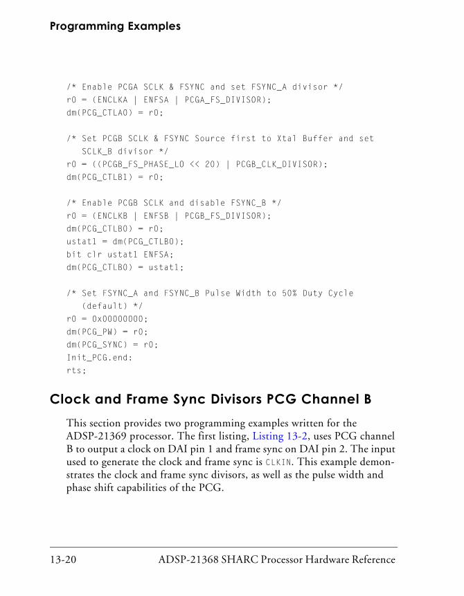
Programming Examples
13-20 ADSP-21368 SHARC Processor Hardware Reference
/* Enable PCGA SCLK & FSYNC and set FSYNC_A divisor */
r0 = (ENCLKA | ENFSA | PCGA_FS_DIVISOR);
dm(PCG_CTLA0) = r0;
/* Set PCGB SCLK & FSYNC Source first to Xtal Buffer and set
SCLK_B divisor */
r0 = ((PCGB_FS_PHASE_LO << 20) | PCGB_CLK_DIVISOR);
dm(PCG_CTLB1) = r0;
/* Enable PCGB SCLK and disable FSYNC_B */
r0 = (ENCLKB | ENFSB | PCGB_FS_DIVISOR);
dm(PCG_CTLB0) = r0;
ustat1 = dm(PCG_CTLB0);
bit clr ustat1 ENFSA;
dm(PCG_CTLB0) = ustat1;
/* Set FSYNC_A and FSYNC_B Pulse Width to 50% Duty Cycle
(default) */
r0 = 0x00000000;
dm(PCG_PW) = r0;
dm(PCG_SYNC) = r0;
Init_PCG.end:
rts;
Clock and Frame Sync Divisors PCG Channel BThis section provides two programming examples written for the ADSP-21369 processor. The first listing, Listing 13-2, uses PCG channel B to output a clock on DAI pin 1 and frame sync on DAI pin 2. The input used to generate the clock and frame sync is CLKIN. This example demon-strates the clock and frame sync divisors, as well as the pulse width and phase shift capabilities of the PCG.

ADSP-21368 SHARC Processor Hardware Reference 13-21
Precision Clock Generators
Listing 13-2. PCG Channel B Output Example
/* Register Definitions */
#define SRU_CLK4 0x2434
#define SRU_PIN0 0x2460
#define SRU_PBEN0 0x2478
#define PCG_CTLB0 0x24C2
#define PCG_CTLB1 0x24C3
#define PCG_PW 0x24C4
/* SRU Definitions */
#define PCG_CLKB_P 0x39
#define PCG_FSB_P 0x3B
#define PBEN_HIGH_Of 0x01
//Bit Positions
#define DAI_PB02 7
#define DAI_PBE02 6
#define PCG_PWB 16
/* Bit Definitions */
#define ENFSB 0x40000000
#define ENCLKB 0x80000000
/* Main code section */
.global _main;
.section/pm seg_pmco;
_main:
/* Route PCG Channel B clock to DAI Pin 1 via SRU */
/* Route PCG Channel B frame sync to DAI Pin 2 via SRU */
r0 = PCG_CLKB_P|(PCG_FSB_P<<DAI_PBE02);
dm(SRU_PIN0) = r0;
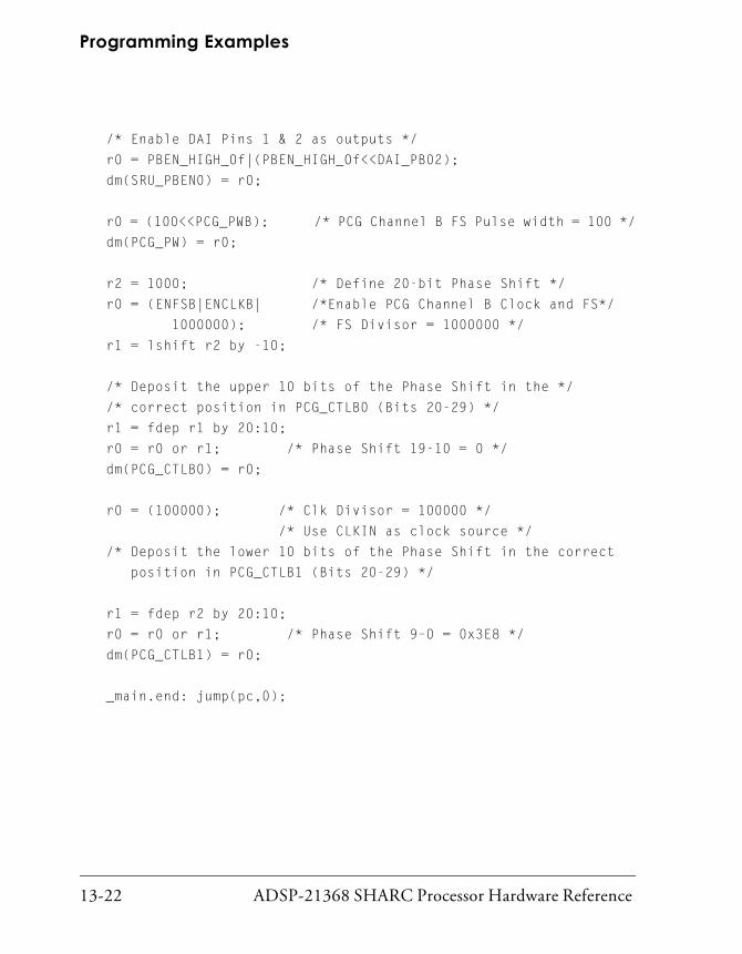
Programming Examples
13-22 ADSP-21368 SHARC Processor Hardware Reference
/* Enable DAI Pins 1 & 2 as outputs */
r0 = PBEN_HIGH_Of|(PBEN_HIGH_Of<<DAI_PB02);
dm(SRU_PBEN0) = r0;
r0 = (100<<PCG_PWB); /* PCG Channel B FS Pulse width = 100 */
dm(PCG_PW) = r0;
r2 = 1000; /* Define 20-bit Phase Shift */
r0 = (ENFSB|ENCLKB| /*Enable PCG Channel B Clock and FS*/
1000000); /* FS Divisor = 1000000 */
r1 = lshift r2 by -10;
/* Deposit the upper 10 bits of the Phase Shift in the */
/* correct position in PCG_CTLB0 (Bits 20-29) */
r1 = fdep r1 by 20:10;
r0 = r0 or r1; /* Phase Shift 19-10 = 0 */
dm(PCG_CTLB0) = r0;
r0 = (100000); /* Clk Divisor = 100000 */
/* Use CLKIN as clock source */
/* Deposit the lower 10 bits of the Phase Shift in the correct
position in PCG_CTLB1 (Bits 20-29) */
r1 = fdep r2 by 20:10;
r0 = r0 or r1; /* Phase Shift 9–0 = 0x3E8 */
dm(PCG_CTLB1) = r0;
_main.end: jump(pc,0);

ADSP-21368 SHARC Processor Hardware Reference 13-23
Precision Clock Generators
PCG Channel A and B Output ExampleListing 13-3 uses two PCG channels. Channel A is set up to only generate a clock signal. This clock signal is used as the input to channel B through SRU1. The clock and frame sync are routed to DAI pins 1 and 2, respec-tively, in the same manner as Listing 13-1. The frame sync generated in this example is set for a 50% duty cycle, with no phase shift.
Listing 13-3. PCG Channel A and B Output Example
/* Register Definitions */
#define SRU_CLK4 0x2434
#define SRU_PIN0 0x2460
#define SRU_PBEN0 0x2478
#define PCG_CTLA0 0x24C0
#define PCG_CTLA1 0x24C1
#define PCG_CTLB0 0x24C2
#define PCG_CTLB1 0x24C3
#define PCG_PW 0x24C4
/* SRU Definitions */
#define PCG_CLKA_O 0x1c
#define PCG_CLKB_P 0x39
#define PCG_FSB_P 0x3B
#define PBEN_HIGH_Of 0x01
//Bit Positions
#define PCG_EXTB_I 5
#define DAI_PB02 7
#define DAI_PBE02 6
#define PCG_PWB 16

Programming Examples
13-24 ADSP-21368 SHARC Processor Hardware Reference
/* Bit Definitions */
#define ENCLKA 0x80000000
#define ENFSB 0x40000000
#define ENCLKB 0x80000000
#define CLKBSOURCE 0x80000000
#define FSBSOURCE 0x40000000
/* Main code section */
.global _main; /* Make main global to be accessed by ISR */
.section/pm seg_pmco;
_main:
/*Route PCG Channel A clock to PCG Channel B Input via SRU*/
r0 = (PCG_CLKA_O<<PCG_EXTB_I);
dm(SRU_CLK4) = r0;
/* Route PCG Channel B clock to DAI Pin 1 via SRU */
/* Route PCG Channel B frame sync to DAI Pin 2 via SRU */
r0 = (PCG_CLKB_P|(PCG_FSB_P<<DAI_PEB02));
dm(SRU_PIN0) = r0;
/* Enable DAI Pins 1 & 2 as outputs */
r0 = (PBEN_HIGH_Of|(PBEN_HIGH_Of<<DAI_PB02));
dm(SRU_PBEN0) = r0;
r0 = ENCLKA; /* Enable PCG Channel A Clock, No Channel A FS */
/* FS Divisor = 0, FS Phase 10-19 = 0 */
dm(PCG_CTLA0) = r0;
r1 = 0xfffff; /* Clk Divisor = 0xfffff, FS Phase 0-9 = 0 */
/* Use CLKIN as clock source */
dm(PCG_CTLA1) = r1;
r0 = (5<<PCG_PWB); /* PCG Channel B FS Pulse width = 1 */
dm(PCG_PW) = r0;

ADSP-21368 SHARC Processor Hardware Reference 13-25
Precision Clock Generators
r0 = (ENFSB|ENCLKB|10); /*Enable PCG Channel B Clock and FS*/
/* FS Divisor = 10, FS Phase 10-19 = 0 */
dm(PCG_CTLB0) = r0;
r0 = (CLKBSOURCE|FSBSOURCE|10); /* Clk Divisor = 10 */
/* FS Phase 0-9 = 0, Use SRU_MISC4 as clock source */
dm(PCG_CTLB1) = r0;
_main.end: jump(pc,0);

Programming Examples
13-26 ADSP-21368 SHARC Processor Hardware Reference

ADSP-21368 SHARC Processor Hardware Reference 14-1
14 SYSTEM DESIGN
The ADSP-21367/8/9 and ADSP-2137x processors support many system design options. The options implemented in a system are influenced by cost, performance, and system requirements. This chapter provides the following system design information:
• “Processor Pin Descriptions” on page 14-2
• “Clock Derivation” on page 14-13. Includes “Power Management Control Register”, “Phase-Locked Loop Startup”, “RESET and CLKIN”.
• “Conditioning Input Signals” on page 14-32
• “Designing for High Frequency Operation” on page 14-33
• “Booting” on page 14-37
• “Data Delays, Latencies, and Throughput” on page 14-52
Other chapters also discuss system design issues. Some other locations for system design information include:
• “SPORT Operation Modes” on page 5-10
• “SPI General Operations” on page 6-8
By following the guidelines described in this chapter, you can ease the design process for your ADSP-21367/8/9 and ADSP-2137x processor product. Development and testing of your application code and hardware can begin without debugging the debug port.

Processor Pin Descriptions
14-2 ADSP-21368 SHARC Processor Hardware Reference
Before proceeding with this chapter it is recommended that you become familiar with the ADSP-21367/8/9 and ADSP-2137x pro-cessor’s core architecture. This information is presented in the ADSP-2136x SHARC Processor Programming Reference.
Processor Pin DescriptionsRefer to the processor-specific data sheet for pin information, including package pinouts for the currently available package options.
Pin MultiplexingThe ADSP-21367/8/9 and ADSP-2137x processors provide the same functionality as other SHARC processors but with a much lower pin count (reducing system cost). Pin multiplexing is used in the following ways.
• Reset output/local clock output/running reset input (ADSP-2137x processors only)
For more information, see “RESETOUT/CLKOUT/RUNRSTIN” on page 14-12.
• External memory interface data (input/output)
For more information, see “Choosing EP Data Mode” on page 14-6.
• PDAP (input only)
• FLAGS (input/output)
For more information, see “Core-Based Flag Pins” on page 14-8.
• PWM channels (output, not available on all models)
See Table 1-1 on page 1-5.

ADSP-21368 SHARC Processor Hardware Reference 14-3
System Design
The processors also include the multiplexers for FLAG0–3 pins. The FLAG0–2 pins can act as core FLAGS0–2 or IRQ0–2, and the FLAG3 pin can act as a core FLAG3 or as the TMREXPEN signal of the system timer.
Table 14-1 on page 14-7 shows the SYSCTL register bit settings for the dif-ferent data pin functions, and Figure 14-1 and Figure 14-2 show the block diagrams of data pin multiplexing in the ADSP-21367/8/9 and ADSP-2137x processors respectively. Note that:
• In the PDAP control register (IDP_PP_CTL), the IDP_EP_SELECT bit (bit 26) is the logical AND of the IDP_PDAP_EN bit (bit 31). When IDP_EP_SELECT is set (= 1), the data bits are read from DATA31–12 and the control signals come from DATA11-8. When IDP_EP_SELECT is cleared (= 0), the data bits are read from DAI_P20–1. When IDP_EP_SELECT is set to 1, the PDAP can be operated through data pins alone (data and controls are completely routed through data pins). For bit descriptions, see “Parallel Data Acquisition Port Control Register (IDP_PP_CTL)” on page A-74.
• The PDAP, PWM, and memory-to-memory (MTM_DATA) signals can be mapped only to the upper bits of the data pins. Therefore, they can be used even when 8- or 16-bit external SRAM is used.
• The FLAGS and PWM can be mapped (in groups of four) to any of upper 16 data pins. The FLAGS alone can be mapped to any of the 32 data pins.
• For PDAP mode, the SYSCTL register must be explicitly pro-grammed to put DATA pins in PDAP mode. For bit descriptions, see “System Control Register (SYSCTL)” on page A-5.
• By default, after reset, all data pins are in external memory mode and the FLAG0-3 pins are in FLAGS mode.

Processor Pin Descriptions
14-4 ADSP-21368 SHARC Processor Hardware Reference
Figure 14-1. Block Diagram of Data Pin Multiplexing (ADSP-2136x)
F LAG S3-0
FLAG S7-4
3-0
7-4
11-8
15-12
P W M 3-0
P W M 7-4
FLAG S11-8
PW M 11-8
FLAGS15-12
PW M 15-12
FLAG S/PW M 15-0D
AT
A31-
0
0
7
15
31EP_DATA 16-31
PDAP_DATA15-0
FLAG S/PW M 15-0
M TM _DATA15-0
EP_DATA8-15
PDAP_DAT A/CTRL
F LAGS8-15
EP_DATA7-0
FL AGS7-0

ADSP-21368 SHARC Processor Hardware Reference 14-5
System Design
Figure 14-2. Block Diagram of Data Pin Multiplexing (ADSP-2137x)
FLAGS3-0
FLAGS7-4
3-0
7-4
11-8
15-12
PWM3-0
PWM7-4
FLAGS11-8
PWM11-8
FLAGS15-12
PWM15-12
FLAGS/PWM15-0
DA
TA
31-0
0
7
15
31EP_DATA16-31
PDAP_DATA15-0
FLAGS/PWM15-0
MTM_DATA15-0
EP_DATA8-15
PDAP_DATA/CTRL
FLAGS8-15
EP_DATA7-0
FLAGS7-0
FLAG0
IRQ0
FLAG0FLAG1FLAG2FLAG3
FLAG0 PIN
FLAG1 PIN
FLAG2 PIN
FLAG3 PIN
FLAG1
IRQ1
FLA2
IRQ2
FLAG0
TIMEXP
MS2
MS2
AD
DR
23-0
23
0
FROM EXTERNALPORT
NOTE: ONLY 16 DATA LINES (DATA15-0)ARE AVAILABLE ON THE ADSP-21375.

Processor Pin Descriptions
14-6 ADSP-21368 SHARC Processor Hardware Reference
Choosing EP Data Mode
The FLAG/IRQ (0, 1, 2, 3) and DATA31–0 pins are completely independent. Any mode of programming in one group does not affect the other.
Case 1
If 32-bit external SDRAM/FLASH/SRAM is used, then all data pins should be connected to the memory device so that no other functionality can be programmed in the data pins. In this case, use MODE 0. If flags are required, they can be moved to the DPI SRU2.
Case 2
If 16-bit external SDRAM/FLASH/SRAM is used, and if 16 flag inputs are required, then use MODE 1. Since 16 flags are required, set FLAG/PWM_SEL = 0000. The flag input mode should be specified in the FLAGS register.
Case 3
If 16-bit external SDRAM/FLASH/SRAM is used, and if 8 flag outputs and 8 PWM outputs are required, then use MODE 1. Since 8 flags and PWM outputs are required, set FLAG/PWM_SEL = 1100. (In this mode, DATA31–24 are PWM outputs and DATA23–16 are flag outputs.) The flag output mode should be specified in FLAGS register.
Case 4
If 8-bit external SDRAM/FLASH/SRAM is used, and if 8 flag inputs, 8 flag outputs, and 8 PWM outputs are required, then use MODE 2. Since 16 flags are required, then all flags on DATA31–16 are programmed. This means that there are not enough pins left for the PWM outputs (DATA15–8). Therefore, program the PWM outputs on DATA23–16 and program the FLAGS on DATA31–24 and DATA15–8. Set FLAGS/PWM_SEL = 0011. The flag I/O direction should be specified in the FLAGS register.

ADSP-21368 SHARC Processor Hardware Reference 14-7
System Design
Case 5
If no external memory is used, and if the PDAP data lines are connected to DATA pins, and if 8 flags are required, then use MODE 6. Connect the PADP control lines to the DATA pins, and program the flag direction in the FLAGS register.
The upper 32 data pins of the external memory interface are muxed (using bits 23–21 in the SYSCTL register) to support the external memory inter-face data (input/output), the PDAP (input only), the FLAGS (input/output), and the PWM channels (output). Table 14-1 provides the pin settings for these functions.
In PDAP mode, the DATA pins function as follows.
• DATA12–31 pins act as PDAP0–19 (inputs)
• DATA11 pin acts as PDAP HLD (input)
• DATA10 pin acts as PDAP CLK (input)
Table 14-1. Function of Data Pins
SYSCTL bits 23–21 Settings
DATA31–161
1 Not available on the ADSP-21375 processor.
DATA15–8 DATA7–0
000 EPDATA32–0 (default at RESET)
001 FLAGS/PWM15–02
2 These signals can be FLAGS or PWM or a mix of both. However, they can be selected only in groups of four. Their function is determined by the control signals FLAGS/PWM_SEL.
EPDATA15–0
010 FLAGS/PWM15–01 FLAGS15–8 EPDATA7–0
011 FLAGS/PWM15–01 FLAGS15–0
100 PDAP (DATA + CTRL) EPDATA7–0
101 PDAP (DATA + CTRL) FLAGS7–0
110 Reserved
111 Three-state all pins

Processor Pin Descriptions
14-8 ADSP-21368 SHARC Processor Hardware Reference
• DATA9 pin is not used
• DATA8 pin acts as PDAP STROBE (output)
Interrupt and Timer PinsThe processor’s external interrupt pins, flag pins, and timer pin can be used to send and receive control signals to and from other devices in the system. The IRQ2–0 pins are mapped on the FLAG2–0 pins and the TIMEXP pin is mapped on the FLAG3 pin. Hardware interrupt signals (IRQ2–0) are received on the FLAG2–0 pins. Interrupts can come from devices that require the processor to perform some task on demand. A memory-mapped peripheral, for example, can use an interrupt to alert the processor that it has data available. For more information, see Appendix B, Interrupts..
The TIMEXP output is generated by the on-chip timer. It indicates to other devices that the programmed time period has expired. For more informa-tion, see the ADSP-2136x SHARC Processor Programming Reference.
Core-Based Flag PinsThe FLAG3–0 pins allow single bit signalling between the processor and other devices. For example, the processor can raise an output flag to inter-rupt a host processor. Each flag pin can be programmed to be either an input or output. In addition, many processor instructions can be condi-tioned on a flag’s input value, enabling efficient communication and synchronization between multiple processors or other interfaces.
The flags are bidirectional pins and all have the same functionality. The FLGxO bits in the FLAGS register program the direction of each flag pin. For more information, see the ADSP-2136x SHARC Processor Programming Reference.

ADSP-21368 SHARC Processor Hardware Reference 14-9
System Design
When the SPIPDN bit (bit 30 in the PMCTL register) is set (= 1 which shuts down the clock to the SPI), the FLAGx pins cannot be used (through the FLAGS7–0 register bits) because the FLAGx pins are syn-chronized with the clock.
Programming Flags
There are 16 system flags and they can be programmed using the FLAGS register shown in Figure 14-3. Only four flags are connected to FLAG/IRQ0-3 pins after reset. If more flags are required, they can be pro-grammed in the DATA pins (using the SYSCTL register, see Table A-1 on page A-6) or they can be programmed with the SRU2 pins (using SRU2 registers, see “DPI/SRU2 Connection Groups” on page 4-51).
The FLAGS register consists of two bits for each flag, one bit to specify flag direction (or output select) where 0 = input, 1 = output and the other bit to specify the flag’s value. If flags are in input mode, the flag value in FLAGS register is read-only and it shows the input flag status. If flags are in output mode, then the flag value can be written to change output flags and it can also be read to determine the last value written.
FLAGS can be mapped into any of the following three pin groups:
1. Four FLAG/IRQ pins
• Only FLAG0–3 can be mapped.
• Should be programmed through SYSCTL register according to EPDATA mode, IRQxEN, TMREXPEN, and MSEN.
• IRQEN and TMREXPEN take priority over all other modes of these pins.

Processor Pin Descriptions
14-10 ADSP-21368 SHARC Processor Hardware Reference
Figure 14-3. FLAGS Register
31 30 29 28 27 26 25 24 23 22 21 20 19 18 17 16
U0 U 0 U 0 U 0 U 0 U 0 U 0 U 0
FLG15OFLAG15 Output SelectFLG15FLAG15 Value
FLG14OFLAG14 Output Select
FLG14FLAG14 Value
FLG13OFLAG13 Output Select
FLG13FLAG13 Value
FLG12OFLAG12 Output Select
FLG12FLAG12 Value
FLG8FLAG8 ValueFLG8OFLAG8 Output SelectFLG9FLAG9 Value
FLG9OFLAG9 Output SelectFLG10FLAG10 Value
FLG10OFLAG10 Output Select
FLG11FLAG11 Value
FLG11OFLAG11 Output Select
-For all FLGx bits, FLAGx values are as follows: 0=LOW, 1=HIGH.-For all FLGxO bits, FLAGx output selects are as follows: 0=FLAGx Input, 1=FLAGx Output.-U indicates the bit value is unknown at reset.
FLAGS
15 14 13 12 11 10 9 8 7 6 5 4 3 2 1 0
U0 U 0 U 0 U 0 U 0 U 0 U 0 U 0
FLG7OFLAG7 Output SelectFLG7FLAG7 ValueFLG6OFLAG6 Output SelectFLG6FLAG6 ValueFLG5OFLAG5 Output SelectFLG5FLAG5 ValueFLG4OFLAG4 Output SelectFLG4FLAG4 Value
FLG0FLAG0 Value
FLG0OFLAG0 Output SelectFLG1FLAG1 Value
FLG1OFLAG1 Output Select
FLG2FLAG2 Value
FLG2OFLAG2 Output Select
FLG3FLAG3 Value
FLG3OFLAG3 Output Select

ADSP-21368 SHARC Processor Hardware Reference 14-11
System Design
2. 32 data pins
• All 16 flags can be mapped.
• Can be mapped only in groups of four.
• Should be programmed through the SYSCTL register. For more information, see “System Control Register (SYSCTL)” on page A-5.
3. 14 DPI pins
• 12 flags (FLAG4–15) can be mapped.
• Any flag can go to any DPI pins.
• Should be programmed through the SRU2 registers. For more information, see “DPI/SRU2 Connection Groups” on page 4-51.
The flag data paths from the processor core to the data pin multiplexer block and SRU2 are parallel (Figure 14-1 on page 14-4). Therefore, for FLAGS0–3:
• In output mode, if the same flag is mapped to both data pins and flag pins, then the output comes from both pins.
• In input mode, if the same flag is mapped to both data pins and flag pins, then the input from data pins is given priority.

Processor Pin Descriptions
14-12 ADSP-21368 SHARC Processor Hardware Reference
And for FLAGS4–15:
• In output mode, if the same flag is mapped to both data pins and DPI pins, then the output comes from both pins.
• In input mode, if the same flag is mapped to both data pins and DPI pins, the input from data pins is given priority.
• In input mode, if the same flag is mapped to both upper and lower data pins, the input from the lower data pins is given priority.
RESETOUT/CLKOUT/RUNRSTIN
The default behavior of the RESETOUT pin is to provide a 4096 cycle delay that allows the PLL to lock. In PLL bypass mode, where the CLK_CFG pins = 11, this pin functions as a CLKOUT signal to clock synchronous peripher-als and memory. This can also be accomplished by setting (= 1) bit 12 (CLKOUTEN) in the power management control register and this functional-ity applies to all ADSP-21367/8/9 and ADSP-2137x processors. Finally, on the ADSP-2137x processors only, the RESETOUT pin can configured to provide a running reset. For more information, see “Running Reset (ADSP-2137x)” on page 14-22.
JTAG Interface PinsThe JTAG test access port (TAP) consists of the TCK, TMS, TDI, TDO, and TRST pins. The JTAG port can be connected to a controller that performs a boundary scan for testing purposes. This port is also used by the Analog Devices DSP Tools product line of JTAG emulators and development software to access on-chip emulation features. To allow the use of the emulator, a connector for its in-circuit probe must be included in the tar-get system.

ADSP-21368 SHARC Processor Hardware Reference 14-13
System Design
If the TRST pin is not asserted (or held low) at power-up, the JTAG port is in an undefined state that may cause the processor to drive out on I/O pins that would normally be three-stated at reset. The TRST pin can be held low with a jumper to ground on the target board connector.
A detailed discussion of JTAG and its uses can be found in Engi-neer-to-Engineer Note EE-68, Analog Devices JTAG Emulation Technical Reference. This document is available on the Analog Devices Web site at www.analog.com/processors.
Clock DerivationThe processor uses a PLL (phased-locked loop) to provide clocks that switch at higher frequencies than the system clock (CLKIN). The PLL-based clocking methodology used on the ADSP-21367/8/9 and ADSP-2137x processors influences the clock frequencies and behavior for the serial, SPI, and external ports, in addition to the processor core and internal memory. In each case, the processor PLL provides a non-skewed clock to the core, internal memory, port logic and I/O pins.
The PLL provides a clock that switches at the processor core frequency to the serial ports. Each of the serial ports can be programmed to operate at clock frequencies derived from this clock. The six serial ports’ transmit and receive clocks are divided down from the processor core clock fre-quency by setting the DIVx registers appropriately.
On power-up, the CLKCFG1–0 pins are used to select ratios of 32:1, 16:1, and 6:1. After booting, numerous other ratios (slowing or speeding up the clock) can be selected through software control.

Clock Derivation
14-14 ADSP-21368 SHARC Processor Hardware Reference
Power Management Control RegisterThe ADSP-21367/8/9 and ADSP-2137x processors have a power manage-ment control register (PMCTL) that allows programs to determine the amount of power dissipated. This includes the ability to program the PLL dynamically in software, achieving a slower core instruction rate that min-imizes power use. For a complete register description, see “Power Management Control Register (PMCTL)” on page A-170.
The PMCTL register also allows programs to disable the clock source to a particular processor peripheral, for example the serial ports or the timers, to further conserve power. By default, each peripheral block has its inter-nal clock enabled only after it is initialized. Programs can use the PMCTL register to turn the specific peripheral off after the application no longer needs it. After reset, these peripheral clocks are not enabled until the peripheral itself is initialized by the program. Listing 14-1 and Listing 14-2 show some clock management options.
Listing 14-1. Using the System Clock for the SPI Module
ustat2 = dm(PMCTL);
bit set ustat2 SPIPDN; /* disable internal peripheral clock for
SPI module. SPIPDN is defined as bit
30 of PMCTL */ dm(PMCTL) = ustat2;

ADSP-21368 SHARC Processor Hardware Reference 14-15
System Design
Listing 14-2. PMCTL Example Code
ENABLING CLKOUT:
ustat2 = dm(PMCTL);
bit set ustat2 CLKOUTEN; /* switch pin function from Reset Out
(RSTOUT) to CLKOUT */
dm(PMCTL) = ustat2;
PLL Divisor modification:
ustat2 = dm(PMCTL);
bit clr ustat2 PLLM63|PLLD8; /* clear old multiplier and
divisor*/
bit set ustat2 DIVEN|PLLD8; /* set and enable PLL Divisor for
CoreCLK = CLKIN/8 */
dm(PMCTL) = ustat2;
PLL Multiplier modification:
ustat2 = dm(PMCTL);
bit clr ustat2 PLLM63|PLLD8; /* clear old multiplier and
divisor*/
bit set ustat2 PLLM8 | PLLBP; /* set a multiplier of 8
(default divisor is 2) and put
PLL in Bypass */
dm(PMCTL) = ustat2;
waiting loop:r0 = 4096; /* wait for PLL to lock at new rate
(requirement for modifying
multiplier only) */
lcntr = r0, do pllwait until lce;
pllwait: nop;
ustat2 = dm(PMCTL);
bit clr ustat2 PLLBP; /* take PLL out of Bypass, PLL is
now at CLKIN*4 (CoreCLK = CLKIN *
M/N = CLKIN* 16/4) */
dm(PMCTL) = ustat2;

Clock Derivation
14-16 ADSP-21368 SHARC Processor Hardware Reference
When the PLL is programmed using a multiplier and a divisor, the DIVEN and PLLBP bits should NOT be programmed in the same core clock cycle. There should be a delay of at least one core clock cycle between program-ming these bits. The approaches described below and shown in Listing 14-3, Listing 14-4 and Listing 14-5 can be used to accomplish this.
PLL Programming Examples
Use the following procedure to program the PLL. Please include the corre-sponding processor-specific header definition files def21367.h, def21368.h, def21369.h, def21371.h, def21375.h and cdef21367.h, cdef21368.h, cdef21369.h, cdef21371.h, and cdef21375.h, which contain the register and bit definitions.
1. Set the PLL multiplier and divisor value and enable the divisor by setting the DIVEN bit.
2. After one core clock cycle, place the PLL in bypass mode by setting (= 1) the PLLBP bit.
3. Wait in bypass mode until the PLL locks.
4. Take the PLL out of bypass mode by clearing (= 0) the bypass bit.
Listing 14-3. PLL Programming Example 1
ustat2 = dm(PMCTL);
bit clr ustat2 PLLM63|PLLD8; /* clear old multiplier and
divisor*/
bit set ustat2 DIVEN | PLLD4 |PLLM16; /* set a multiplier of
16 and a divider of 4 */
dm(PMCTL) = ustat2;
bit set ustat2 PLLBP; /* Put PLL in bypass mode. */

ADSP-21368 SHARC Processor Hardware Reference 14-17
System Design
dm(PMCTL) = ustat2;
waiting_loop:
r0 = 4096; /* wait for PLL to lock at new rate
(requirement for modifying
multiplier only) */
lcntr = r0, do pllwait until lce;
pllwait: nop;
ustat2 = dm(PMCTL);
bit clr ustat2 PLLBP; /* take PLL out of Bypass, PLL is now at
CLKIN*4 (CoreCLK = CLKIN * M/N =
CLKIN* 16/4) */
dm(PMCTL) = ustat2;
Use the following alternate procedure to program the PLL.
1. Set the PLL multiplier and divisor values and place the PLL in bypass mode by setting the PLLBP bit.
2. Wait in the bypass mode until the PLL locks.
3. Take the PLL out of bypass mode by clearing the bypass bit.
4. Wait for one core clock cycle.
5. Enable the divisor by setting the DIVEN bit.

Clock Derivation
14-18 ADSP-21368 SHARC Processor Hardware Reference
Listing 14-4. PLL Programming Example 2
ustat2 = dm(PMCTL);
bit clr ustat2 PLLM63|PLLD8; /* clear old multiplier and
divisor*/
bit set ustat2 PLLBP | PLLD4 |PLLM16; /* set a multiplier of 16
and a divider of 4 and
enable Bypass mode*/
ustat2 = dm(PMCTL);
waiting_loop:
r0 = 4096; /* wait for PLL to lock at new rate
(requirement for modifying multiplier only) */
lcntr = r0, do pllwait until lce;
pllwait: nop;ustat2 = dm(PMCTL);
bit clr ustat2 PLLBP; /* take PLL out of Bypass*/
dm(PMCTL) = ustat2;
ustat2 = dm(PMCTL);
bit set ustat2 DIVEN; /* Enable the DIVEN bit, PLL is now at
CLKIN*4 (CoreCLK = CLKIN * M/N = CLKIN* 16/4) */
dm(PMCTL) = ustat2;
Listing 14-5 is a PLL programming example in C.
Listing 14-5. PLL Programming Sequence (C)
pmctlsetting= *pPMCTL;
pmctlsetting &= ~(0xFF); /* Clear */
/* CLKIN= 24.576 MHz, Multiplier= 27, Divisor= 2,
CCLK_SDCLK_RATIO 2. */

ADSP-21368 SHARC Processor Hardware Reference 14-19
System Design
/* Core clock = (24.576 MHz * 27) /2 = 331.776 MHz */
pmctlsetting= SDCKR2|PLLM27|PLLD2|DIVEN;
*pPMCTL= pmctlsetting; pmctlsetting|= PLLBP;
*pPMCTL= pmctlsetting;
pmctlsetting ^= DIVEN;
/* Wait for around 4096 cycles for the pll to lock. */
for (i=0; i<4096; i++)
asm("nop;");
*pPMCTL ^= PLLBP; /* Clear Bypass Mode */
*pPMCTL |= (CLKOUTEN); /* and start clkout */
Phase-Locked Loop StartupThe RESET signal can be held low long enough to guarantee a stable CLKIN source and stable VDDINT/VDDEXT power supplies before the PLL is reset.
The PLL needs time to lock to the CLKIN frequency before the core can execute or begin the boot process. A delayed core reset (RESETOUT) has been added through the delay circuit to provide this time. There is a 12-bit counter that counts up to 4096 CLKIN cycles after RESET is transi-tioned from low to high. This is normally 1.3 μs for the minimum CLKIN frequency. The delay circuit is activated at the same time the PLL is taken out of reset.
The advantage of the delayed core reset is that the PLL can be reset any number of times without having to power down the system. If there is a brownout situation, the watchdog circuit only has to control the RESET.
For more information on device power up, see the processor spe-cific data sheet.

Clock Derivation
14-20 ADSP-21368 SHARC Processor Hardware Reference
RESET and CLKINThe processor receives its clock input on the CLKIN pin. The processor uses an on-chip, phase-locked loop (PLL) to generate its internal clock, which is a multiple of the CLKIN frequency. Because the PLL requires some time to achieve phase lock, CLKIN must be valid for a minimum time period during reset before the RESET signal can be deasserted. For information on minimum clock setup, see the appropriate ADSP-2136x or ADSP-2137x SHARC processor data sheet.
Table 14-2 describes the internal clock to CLKIN frequency ratios sup-ported by the processor. Note that programs control the PLL through the PMCTL register. For more information, see “Power Management Control Register (PMCTL)” on page A-170.
When using an external crystal, the maximum crystal frequency cannot exceed 25 MHz. The internal clock generator, when used in conjunction with the XTAL pin and an external crystal, is designed to support up to a maximum of 25 MHz external crystal frequency. For all other external clock sources, the maximum CLKIN frequency is 50 MHz.
Table 14-3 demonstrates the internal core clock switching frequency across a range of CLKIN frequencies. The minimum operational range for any given frequency may be constrained by the operating range of the phase-lock loop. Note that the goal in selecting a particular clock ratio for
Table 14-2. Pin Selectable Clock Rate Ratios
CLKCFG1-0 Core to CLKIN Ratio
00 6:1
01 32:1
10 16:1

ADSP-21368 SHARC Processor Hardware Reference 14-21
System Design
the application is to provide the highest permissible internal frequency for a given CLKIN frequency. For more information on available clock rates, see the processor-specific data sheet.
Shared memory processor designs that use several ADSP-21368 processors must have the same CLKIN source. These devices should also be brought out of reset together.
If an external master clock is used, it should not drive the CLKIN pin when the processor is not powered. The clock must be driven immediately after power-up; otherwise, internal gates stay in an undefined (hot) state and can draw excess current. After power-up, there should be sufficient time for the oscillator to start up, reach full amplitude, and deliver a stable CLKIN signal to the processor before the reset is released. This may take 100 μs depending on the choice of crystal, operating frequency, loop gain and capacitor ratios. For details on timing, refer to the processor-specific data sheet.
After the external processor RESET signal is deasserted, the PLL starts oper-ating. The rest of the chip is held in reset for 4096 CLKIN cycles after RESET is deasserted by an internal reset signal. This sequence allows the PLL to lock and stabilize. Add one CLKIN cycle if RESET does not meet setup requirements with respect to the CLKIN falling edge.
Table 14-3. Selecting Core to CLKIN Ratio
Typical Crystal and Clock Oscillators Inputs
12.500 16.667 25.000 33.333 40.000 50.000
Clock Ratios Core CLK (MHz)
3:1 N/A N/A N/A 100.000 120.000 150.000
8:1 100 133.33 200.00 266.67 320.00 400.00
16:1 200 266.67 400 N/A N/A N/A
Clock Derivation
14-22 ADSP-21368 SHARC Processor Hardware Reference
Running Reset (ADSP-2137x) All members of the SHARC processor family, including the ADSP-21375 and ADSP-21371, continue to support the hardware reset controlled with the RESET pin. The de-assertion of this hardware reset enables the PLL and asserting it resets the PLL. In the time it takes the PLL to acquire lock (set to 4096 CLKIN cycles), the processor, internal memory, and the peripherals are held in reset. Upon completion of the 4096 CLKIN cycles, the chip is brought out of reset. This is indicated on the RESETOUT/CLKOUT pin for the three valid boot modes (00, 01, 10 settings of BOOT_CFG1-0 pins). For more information, see “Booting” on page 14-37.
In addition to the hardware reset, there is also support for a software reset, which can be asserted by setting bit 0 of the SYSCTL register.
In the ADSP-21375 and ADSP-21371 processors, an additional feature, called running reset, has been added. Running reset resets everything on the chip, including the core and peripheral registers and the program counter (PC). Running reset also clears all stacks and counters. However, it does NOT reset the PLL (like the software reset) and the SDRAM con-troller (to maintain SDRAM auto-refresh). De-assertion of this reset does not result in a boot (unlike any of the other resets) even if a valid boot mode is configured on the BOOT_CFG1-0 pins. Instead, the program counter value is reset to the first location of internal memory (0x90005) and the sequencer begins executing instructions starting from this address.
This feature has been added to allow the ADSP-2137x processors to exe-cute self-modifying code that has previously overwritten existing code in internal memory or as an external watchdog that activates in case there is a malfunction or exception within a peripheral occurs, and a context reset of the processor is sufficient to restore the state, (whereas a complete boot is not required).

ADSP-21368 SHARC Processor Hardware Reference 14-23
System Design
System Design Considerations
It is important that an external 10 kΩ pull-up resistor is placed on the RESETOUT/CLKOUT/RUNRSTOUT pin if it is intended to be used as an input for initiating a running reset on the ADSP-2137x processor as shown in Figure 14-4. Also, it is extremely important to ensure that an external device, such as a micro controller, does not drive this signal during or after coming out of a power-on or hard-reset.
Figure 14-4 shows the active state of the pin during and after RESET. The ADSP-2137x processor is actively driving this pin as an output.
If the system uses an external host or micro controller to control running reset, ensure that the external device waits until the ADSP-2137x proces-sor driver has been internally disabled (by writing to the RUNRSTCTL register) before actively driving this signal at RESET. Connect the CLKOUT pin to an open-drain pin on the host side, or use an external three-state buffer.
Figure 14-4. RESETOUT/CLKOUT Pin Muxed with RUNRSTIN
PADDRIVER
CLKOUT/RESETOUT
RUNRSTIN
+Vdd
10 kΩEnsure that hostprocessor has anopen drain outputand is not activelydriving this pinduring or afterRESET
ADSP-2137x

Clock Derivation
14-24 ADSP-21368 SHARC Processor Hardware Reference
There are several possible methods that can be used to implement running reset. The following illustrates one example of a running reset implemen-tation involving an ADSP-2137x processor and a host processor.
External Host
In an AVR (audio-video receiver) system, a host micro controller may communicate with the ADSP-2137x processor using the serial peripheral interface (SPI). Or, if no SPI pins are available on the host device, it can use spare flag I/Os to connect with the SPI of SHARC as shown in Figure 14-5). In this case, the host implements the SPI protocol on the port pins.
Using the SPI protocol with additional control words and commands, running reset can become an addition command from the host or from the ADSP-2137x processor as described in the following procedure.
1. The host initiates a running reset by informing the processor over the command interface.
Figure 14-5. Example System Interface With an External Host
RUNRSTIN
+Vdd
10 kΩADSP-2137x
SP
IP
OR
T
SP
I OR
P
OR
T P
INS
OpenDrain
Use an external pull-upif host pin does not havean internal pull-up
Host Processor

ADSP-21368 SHARC Processor Hardware Reference 14-25
System Design
2. The ADSP-2137x processor receives the command and completes any unfinished work which may also include writing to the RUN-RSTCTL register.
3. When the ADSP-2137x processor is ready to accept the running reset, it signals the host over the command interface.
4. The host drives the running reset input into the ADSP-21375/71 processor.
Running Reset Control Register (RUNRSTCTL)
To program the running reset feature, (by toggling the RESETOUT pin), a new register, running reset control (RUNRSTCTL) has been added to the ADSP-2137x processor architecture.
This register is located at memory-mapped address 0x2100. On previous generations of SHARCs, the RESETOUT/CLKOUT pin was an output. On the ADSP-2137x processors, this pin is an input/output, and the sense and direction of the pin is controlled by bit 0 of the RUNRSTCTL register (see Table 14-4).
Table 14-4. Running Reset Control Register Bit Descriptions
Bit Name Description
0 PM_RUNRST_PINEN Configures the RESETOUT pin for RUNRST input. Read Write0 = RESETOUT pin is CLKOUT/RESETOUT1 = RESETOUT pin is RUNRST inputReset value = 0
1 PM_RUNRST_EN Enable the running reset functionality.0 = Running reset disabled1 = Running reset enabledReset value = 0
31–2 Reserved Reads return 0Reset value = 0
Clock Derivation
14-26 ADSP-21368 SHARC Processor Hardware Reference
Programming The RUNRSTCTL Register
To configure running reset:
1. Set bit 0 (=1) to change RESETOUT/CLKOUT pin direction to input.
2. Ensure that the RESETOUT/CLKOUT pin is driven to a proper state, and then assert RUNRSTEN to sensitize logic to the state of the RESETOUT/CLKOUT pin.
If bit 1 of the RUNRSTCTL register is not set, attempting to cause a running reset by toggling the RESETOUT/CLKOUT pin does not result in a reset.
The RUNRSTCTL register is reset only on assertion of a hardware reset, software reset, emulator reset, or by writing to the appropri-ate bits of the RUNRSTCTL register via software.
The system reacts to the assertion and recognition of a running reset in the following way.
• The core-PLL is NOT reset, and continues to run
• Internal memory SRAM contents remain unaltered
• The processor core and peripherals are reset exactly as if a Power-on (hardware) reset is asserted, except:
• The SDRAM controller continues to run and refresh as programmed.
• The contents of external SDRAM are unaffected, and retain their values prior to a running reset.
• A system boot is NOT initiated. Instead, the program counter is cleared and program execution begins from the very first location of program memory (from the reset inter-rupt vector table).

ADSP-21368 SHARC Processor Hardware Reference 14-27
System Design
Reset Generators
It is important that a processor (or programmable device) have a reliable active RESET that is released once the power supplies and internal clock cir-cuits have stabilized. The RESET signal should not only offer a suitable delay, but it should also have a clean monotonic edge. Analog Devices has a range of microprocessor supervisory ICs with different features. Features include one or more of the following:
• Power-up reset
• Optional manual reset input
• Power low monitor
• Backup battery switching
The part number series for reset and supervisory circuits from Analog Devices are as follows:
• ADM69x
• ADM70x
• ADM80x
• ADM1232
• ADM181x
• ADM869x
A simple power-up reset circuit is shown in Figure 14-6 using the ADM809-RART reset generator. The ADM809 provides an active low RESET signal whenever the supply voltage is below 2.63 V. At power-up, a 240 μs active reset delay is generated to give the power supplies and oscil-lators time to stabilize.

Clock Derivation
14-28 ADSP-21368 SHARC Processor Hardware Reference
Another part, the ADM706TAR, provides power on RESET and optional manual RESET. It allows designers to create a more complete supervisory circuit that monitors the supply voltage. Monitoring the supply voltage allows the system to initiate an orderly shutdown in the event of power failure. The ADM706TAR also allows designers to create a watchdog timer that monitors for software failure. This part is available in an 8-lead SOIC package. Figure 14-7 shows a typical application circuit using the ADM706TAR.
Timing SpecificationsThe ADSP-21367/8/9 and ADSP-2137x processor’s internal clock (a mul-tiple of CLKIN) provides the clock signal for timing internal memory, processor core, serial ports, and SPI (as required for read/write strobes). During reset, program the ratio between the processor’s internal clock fre-quency and external (CLKIN) clock frequency with the CLK_CFG1–0 pins.
Figure 14-6. Simple Reset Generator
VCC
RESET
GND
ADM809-RART
VDDEXT
RESET
GND
+3.3VDDEXT
10µF
VDDINT
+1.2VDDINT
aADSP-213xxS

ADSP-21368 SHARC Processor Hardware Reference 14-29
System Design
To determine switching frequencies for the serial ports, divide down the internal clock, using the programmable divider control of each port (DIVx for the serial ports). For the SPI port, the BAUDR bit in the SPICTL register controls the SPICLK baud rate based on the core clock frequency.
Note the following definition and Figure 14-8 for various clock periods that are functions of CLKIN and the appropriate ratio control:
CCLK = core clock = PLLICLK × PLL multiply ratio (determined by CLK_CFG pins)
Programs can modify this setting using bits in the PMCTL register. For more information, see “Power Management Control Register (PMCTL)” on page A-170.
Performing a hard reset on the processor also resets the PLL.
Figure 14-7. Reset Generator and Power Supply Monitor
RESET
NMI
IRQx
FLAGx
GNDRESET
VDDEXT
PFI
OSCSEL
PFO
WDI
WDO
4
8
7
15
11
14
ADM8697
VCC9
RST
10
VDDEXT +3.3V
aADSP-213xxS
3
15
OSCIN
GND TST
LLW
NC3.3V
Vt> 1.3V
Vt> 1.3V
VLINE SENSE

Clock Derivation
14-30 ADSP-21368 SHARC Processor Hardware Reference
Figure 14-8. Core Clock and System Clock Relationship to CLKIN
Table 14-5. CLKOUT and CCLK Clock Generation Operation
Timing Requirements
Calculation Description
CLKIN = 1/tCKIN = Input Clock
CLKOUT = 1/tTCK = Local Clock Out
PLLICLK = 1/tPLLIN = PLL Input Clock
CCLK = 1/tCCLK = Core Clock
÷2+
–
0
1
INDIV[8]
LOOPFILTER
VCO ÷1, 2, 4, 8
NPLLD[7..6]
DIVEN[9]
01
1
PLLBP[15]
AMP
÷1-64
MPLLM[5..0]
CLK
_C
FG
[1..0
]
00 = x6
01 = x32
10 = x16
11 = x6
DELAY4096 x CLKIN
CLKOUTEN[12]
BUFF
÷2
0
1
CCLK100 MHz
to400 MHz
PCLK(IOP)
CLKOUTor
CORERST
RESETOUT
CLKIN(see data sheet)
RESET
XTAL
BOOT CLKCFG[]->PLLM[] CFG
Notes1. CLKOUT is muxed with RESETOUT. After reset, RESETOUT is selected. CLKOUT is selected by setting bit 12 in the PMCTL register.2.The PLL ratio is controlled by the states of the CLKCFG[1:0] pins at reset and can be modified in software through thePLLMand PLLDx bits in the PMCTL register.3.To place the PLL in bypass mode, set bit 15 in the PMCTL register. (CCLK = PLLICLK when set.)4. Programs can interrupt the internal clock source to each of the following peripherals: timer, SPI, SPORTs, and parallel port.These internal clock sources are disabled at reset and are enabled and left enabled after each peripheral is enabled.Note that these peripherals DO NOT RUN at the core clock frequency. For more information please see the respective peripheralchapters in the ADSP-2136x SHARC Processor Hardware Reference.5. Please refer to the processor specific data sheets for maximum CLKIN and crystal source specifications.
160 MHz < VCO_OUT < 800 MHz
÷2, 2.5,3, 3.5, 4 SDCLK
SDRATIO[20..18]
PLL BYP ASS; Reserved
CL
KC
FG
[1..
0]
MULTIPLIERBLOCK

ADSP-21368 SHARC Processor Hardware Reference 14-31
System Design
Table 14-7 describes clock ratio requirements. Table 14-8 shows an exam-ple clock derivation.
Table 14-6. Clock Relationships
Timing Requirements
Description1
tCK = CLKOUT Clock Period
tPLLICK = PLL Input Clock
tCCLK = Core Clock Period (Processor)
tPCLK = Peripheral Clock Period = 2 × tCCLK
tSCLK = Serial Port Clock Period = (tPCLK) × SR
tSPICLK = SPI Clock Period = (tCCLK) * SPIR
1 where:SR = serial port-to-core clock ratio (wide range, determined by CLKDIV)SPIR = SPI-to-core clock ratio (wide range, determined by SPICTL register)SCLK = serial port clockSPICLK = SPI clock
Table 14-7. Clock Ratios
Timing Requirements
Description
cRTO = Core to CLKOUT ratio (3:1, 8:1, or 16:1, determined by CLK_CFGx pins at reset). Programs can modify this ratio using the PMCTL register.
sRTO = Sport:core clock ratio (wide range determined by xCLKDIV)
Table 14-8. Clock Derivation
Timing Requirements
Description
tCCLK = (tCK) × cRTO
tSCLK = (tCCLK) × sRTO

Conditioning Input Signals
14-32 ADSP-21368 SHARC Processor Hardware Reference
Input Synchronization DelayThe processor has several asynchronous inputs—RESET, TRST, IRQ2–0, MS3–0, and FLAG16-0 (when configured as inputs). These inputs can be asserted in arbitrary phase to the processor clock, CLKIN. The processor synchronizes the inputs prior to recognizing them. The delay associated with recognition is called the synchronization delay.
Any asynchronous input must be valid prior to the recognition point in a particular cycle. If an input does not meet the setup time on a given cycle, it may be recognized in the current cycle or during the next cycle.
To ensure recognition of an asynchronous input, it must be asserted for at least one full processor cycle plus setup and hold time, except for RESET, which must be asserted for at least four processor cycles. The minimum time prior to recognition (the setup and hold time) is specified in the pro-cessor’s data sheet.
Conditioning Input SignalsThe processor is a CMOS device. It has input conditioning circuits which simplify system design by filtering or latching input signals to reduce sus-ceptibility to glitches or reflections.
The following sections describe why these circuits are needed and their effect on input signals.
A typical CMOS input consists of an inverter with specific N and P device sizes that cause a switching point of approximately 1.4 V. This level is selected to be the midpoint of the standard TTL interface specification of VIL = 0.8 V and VIH = 2.0 V. This input inverter, unfortunately, has a fast response to input signals and external glitches wider than 1 ns. Filter cir-cuits and hysteresis are added after the input inverter on some processor inputs, as described in the following sections.

ADSP-21368 SHARC Processor Hardware Reference 14-33
System Design
RESET Input HysteresisHysteresis is used only on the RESET input signal. Hysteresis causes the switching point of the input inverter to be slightly above 1.4 V for a rising edge and slightly below 1.4 V for a falling edge. The value of the hysteresis is approximately ± 0.1 V. The hysteresis is intended to prevent multiple triggering of signals which are allowed to rise slowly, as might be expected on a reset line with a delay implemented by an RC input circuit. Hystere-sis is not used to reduce the effect of ringing on processor input signals with fast edges, because the amount of hysteresis that can be used on a CMOS chip is too small to make a difference. The small amount of hys-teresis allowable is due to the restrictions on the tolerance of the VIL and VIH TTL input levels under worst-case conditions. Refer to the prod-uct-specific processor data sheet for exact specifications.
Designing for High Frequency OperationBecause the processor must be able to operate at very high clock frequen-cies, signal integrity and noise problems must be considered for circuit board design and layout. The following sections discuss these topics and suggest various techniques to use when designing and debugging target systems.
All synchronous processor behavior is specified to CLKIN. System designers are encouraged to clock synchronous peripherals with this same clock source (or a different low-skew output from the same clock driver).
Clock Specifications and JitterThe clock signal must be free of ringing and jitter. Clock jitter can easily be introduced into a system where more than one clock frequency exists. Jitter should be kept to an absolute minimum. High frequency jitter on the clock to the processor may result in abbreviated internal cycles.

Designing for High Frequency Operation
14-34 ADSP-21368 SHARC Processor Hardware Reference
Keep the portions of the system that operate at different frequencies as physically separate as possible. The clock supplied to the processor must have a rise time of 3 ns or less and must meet or exceed a high and low voltage of 2 V and 0.4 V, respectively.
Never share a clock buffer IC with a signal of a different clock fre-quency as this introduces excessive jitter.
Other Recommendations and Suggestions• Use more than one ground plane on the PCB to reduce crosstalk.
Be sure to use lots of vias between the ground planes. One VDD plane for each supply is sufficient. These planes should be in the center of the PCB.
• To reduce crosstalk, keep critical signals such as clocks, strobes, and bus requests on a signal layer next to a ground plane and away from these signals, or layout critical signals perpendicular to other non-critical signals.
• If possible, position the processors on both sides of the board to reduce area and distances.
• To allow better control of impedance and delay, and to reduce crosstalk, design for lower transmission line impedances.
• Use 3.3 V peripheral components and power supplies to help reduce transmission line problems, ground bounce and noise cou-pling (the receiver switching voltage of 1.5 V is close to the middle of the voltage swing).
• Experiment with the board and isolate crosstalk and noise issues from reflection issues. This can be done by driving a signal wire from a pulse generator and studying the reflections while other components and signals are passive.

ADSP-21368 SHARC Processor Hardware Reference 14-35
System Design
Decoupling Capacitors and Ground PlanesExtended copper planes must be used for the ground and power supplies. Designs should use an absolute minimum of 12 bypass capacitors (four 0.1 μF, four 10 nF and four 1 nF ceramic) for each VDDEXT and VDDINT supply. More extensive bypassing may be required for some applications. The capacitors should be placed close to the package as shown in Figure 14-9. The decoupling capacitors should be tied directly to the power and ground planes with vias that touch their solder pads. Sur-face-mount capacitors are recommended because of their lower series inductances (ESL) and higher series resonant frequencies. Connect the power and ground planes to the ADSP-21367/8/9 and ADSP-2137x pro-cessor’s power supply pins directly with vias—do not use traces. The ground planes should not be densely perforated with vias or traces as this reduces their effectiveness. In addition, there should be several large tanta-lum capacitors on the board.
Designs can use either bypass placement case shown in Figure 14-9, or combinations of the two. Designs should try to minimize signal feedthroughs that perforate the ground plane.
Oscilloscope ProbesWhen making high speed measurements, be sure to use a “bayonet”-type ground clip (or similarly short, < 0.5 inch), attached to the tip of the oscil-loscope probe. The probe should be a low capacitance active probe with 3 pF or less of loading. The use of a standard ground clip with 4 inches of ground lead causes ringing to be seen on the displayed trace and makes the signal appear to have excessive overshoot and undershoot. A 1 GHz or better sampling oscilloscope is needed to see the signals accurately.

Designing for High Frequency Operation
14-36 ADSP-21368 SHARC Processor Hardware Reference
Recommended ReadingThe text High-Speed Digital Design: A Handbook of Black Magic is recom-mended for further reading. This book is a technical reference that covers the problems encountered in state-of-the-art, high frequency digital cir-cuit design. It is also an excellent source of information and practical ideas. Topics covered in the book include:
• High-Speed Properties of Logic Gates
• Measurement Techniques
• Transmission Lines
Figure 14-9. Bypass Capacitor Placement
CASE 1:BYPASS CAPACITORS ON NON-COMPONENT(BOTTOM) SIDE OF BOARD, BENEATH DSPPACKAGE
aADSP-213xx
S
CASE 2:BYPASS CAPACITORS ON COMPONENT (TOP)SIDE OF BOARD, AROUND DSP PACKAGE
ADSP-21368 SHARC Processor Hardware Reference 14-37
System Design
• Ground Planes and Layer Stacking
• Terminations
• Vias
• Power Systems
• Connectors
• Ribbon Cables
• Clock Distribution
• Clock Oscillators
High-Speed Digital Design: A Handbook of Black Magic, Johnson & Gra-ham, Prentice Hall, Inc., ISBN 0-13-395724-1.
BootingWhen a processor is initially powered up, its internal SRAM is undefined. Before actual program execution can begin, the application must be loaded from an external non-volatile source such as flash memory or a host processor. This process is known as bootstrap loading or booting and is automatically performed by the processor after power-up or after a soft-ware reset.
The ADSP-21367/8/9 and ADSP-2137x processors support three booting modes—EPROM, SPI master and SPI slave. Each of these modes uses the following general procedure:
1. At reset, the processor is hardwired to load 256 48-bit instruction words through a DMA starting at location 0x90000. In this sec-tion, these instructions are referred to as the boot kernel or loader kernel.

Booting
14-38 ADSP-21368 SHARC Processor Hardware Reference
2. The DMA completes and the interrupt associated with the periph-eral that the processor is booting from is activated. The processor jumps to the applicable interrupt vector location and executes the code located there. (Typically, the first instruction at the interrupt vector is a return from interrupt (RTI) instruction.)
3. The loader kernel executes a series of direct memory accesses (DMAs) to import the rest of the application, overwriting itself with the applications’ interrupt vector table (IVT).
4. After executing the kernel, the processor returns to location 0x90005 where normal program execution begins.
To support this process, a 256-word loader kernel and loader (which con-verts executables into boot-loader images) are supplied with the VisualDSP++ development tools for both SPI and external port booting. For more information on the loader, see the tools documentation in Related Documents on page xxxviii.
The boot source is determined by strapping the two BOOT_CFG1-0 pins to either logic low or logic high. These settings are shown in Table 14-9.
Table 14-9. Booting Modes
BOOT_CFG1-0 Description
00 SPI Slave Boot
01 SPI Master Boot
10 EPROM/FLASH Boot Through The External Port
11 Bypass Mode, Reserved

ADSP-21368 SHARC Processor Hardware Reference 14-39
System Design
External Port BootingThe ADSP-21367/8/9 processors allow booting through the external port. There are two options, which are described in the following sections.
Booting Through the AMI
The asynchronous memory interface (AMI) supports an 8-bit user boot called AMI boot. Only the MS1 signal is used for AMI(FLASH/EEPROM) booting. Table 14-10 shows the bit settings for AMI boot. These bits are described in detail in “AMI Control Registers (AMICTLx)” on page A-17.
Table 14-10. AMI Boot Bit Settings (AMICTLx)
Bit Setting
AMI Enable (AMIEN) 1
Bus Width (BW) 00
Packing Disabled (PKDIS) 0
Most Significant Word First (MSWF) 0
ACK Pin Enable (ACKEN) 0
Wait States (WS) 10111
Bus Hold Cycle at the End of Write Access (HC) 000
Idle Cycle (IC) 000
Buffer Flush (FLSH) 0
Read Hold Cycle at the End of Read Access (RHC) 000
Disable Predictive Reads (NO_OPT) 0

Booting
14-40 ADSP-21368 SHARC Processor Hardware Reference
Shared Memory Booting
To boot multiple processors from a single EPROM/FLASH, the processor performs the following steps.
1. Arbitrate for the bus.
2. Receive through DMA the 256-word boot kernel, after becoming bus master.
3. Release the bus, allowing the next processor access to the EPROM/FLASH.
4. Execute the loaded instructions. These usually consist of the boot kernel, which brings in the remaining application code.
For more information on developing executables for shared-memory boot-ing, see the VisualDSP++ Loader Manual or the VisualDSP++ Loader and Linker Manual (depending on the VisualDSP++ release you are using).
The MS1 signals from each processor may be wire ORed together to drive the chip select pin of the EPROM. Each processor boots in turn, accord-ing to its priority. When the last processor has finished booting, it must inform the others (which may be in the idle state) that program execution can begin (if all the processors are to begin executing instructions simulta-neously). An example system that uses an alternating technique appears in Figure 14-10. When multiple processors boot from one EPROM, they can boot either identical code or different code from the EPROM.

ADSP-21368 SHARC Processor Hardware Reference 14-41
System Design
Figure 14-10. Alternating Booting From an EPROM
ADSP-21368
MS
RD
DATA
ADDR
ADSP-21368
MS
RD
DATA
ADDR
ADSP-21368
MS
RD
DATA
ADDR
ADSP-21368
MS
RD
DATA
ADDR
CO
NT
RO
L
AD
DR
ES
S
DA
TA
EPROM
RD
DATA
ADDR
CS

Booting
14-42 ADSP-21368 SHARC Processor Hardware Reference
SPI Port BootingThe ADSP-21367/8/9 and ADSP-2137x processors support booting from a host processor through the SPI slave (BOOT_CFG1–0 = 00), and booting from an SPI flash, SPI PROM, or a host processor through SPI master mode (BOOT_CFG1–0 = 01).
The SPI can also be configured to boot using the pins in the digital peripheral interface. For more information, see “DPI/SRU2 Con-nection Groups” on page 4-51.
Both SPI boot modes support booting from 8-, 16-, or 32-bit SPI devices. In all SPI boot modes, the data word size in the shift register is hardwired to 32 bits. Therefore, for 8- or 16-bit devices, data words are packed into the shift register to generate 32-bit words least significant bit (LSB) first, which are then shifted into internal memory. The relationship between the 32-bit words received into the RXSPI register and the instructions that need to be placed in internal memory is shown in Figure 14-11.
For more information about 32- and 48-bit internal memory addressing, see the “Memory” chapter in the ADSP-2136x SHARC Processor Program-ming Reference.
Figure 14-11. SPI Data Packing
MOSI
32-b
it R
ecei
veS
hift
Reg
iste
r
SP
IRx
DMAInternalMemory
32 32 32
0x900FF
0x90000
256 48-bitWords
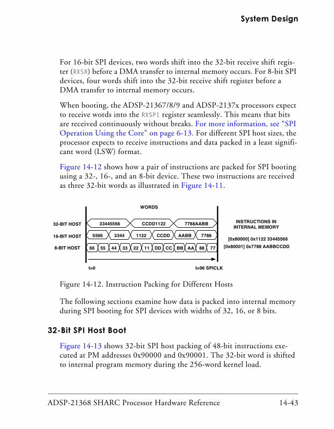
ADSP-21368 SHARC Processor Hardware Reference 14-43
System Design
For 16-bit SPI devices, two words shift into the 32-bit receive shift regis-ter (RXSR) before a DMA transfer to internal memory occurs. For 8-bit SPI devices, four words shift into the 32-bit receive shift register before a DMA transfer to internal memory occurs.
When booting, the ADSP-21367/8/9 and ADSP-2137x processors expect to receive words into the RXSPI register seamlessly. This means that bits are received continuously without breaks. For more information, see “SPI Operation Using the Core” on page 6-13. For different SPI host sizes, the processor expects to receive instructions and data packed in a least signifi-cant word (LSW) format.
Figure 14-12 shows how a pair of instructions are packed for SPI booting using a 32-, 16-, and an 8-bit device. These two instructions are received as three 32-bit words as illustrated in Figure 14-11.
The following sections examine how data is packed into internal memory during SPI booting for SPI devices with widths of 32, 16, or 8 bits.
32-Bit SPI Host Boot
Figure 14-13 shows 32-bit SPI host packing of 48-bit instructions exe-cuted at PM addresses 0x90000 and 0x90001. The 32-bit word is shifted to internal program memory during the 256-word kernel load.
Figure 14-12. Instruction Packing for Different Hosts
16-BIT HOST
CCDD1122
1122
33445566 7788AABB
CCDD AABB 778833445566
66 55 44 33 22 11 DD CC BB AA 88 77
32-BIT HOST
8-BIT HOST
[0x80000] 0x1122 33445566
[0x80001] 0x7788 AABBCCDD
WORDS
INSTRUCTIONS ININTERNAL MEMORY
t=0 t=96 SPICLK

Booting
14-44 ADSP-21368 SHARC Processor Hardware Reference
The following example shows a 48-bit instructions executed.
[0x90000] 0x112233445566
[0x90001] 0x7788AABBCCDD
The 32-bit SPI host packs or prearranges the data as:
16-Bit SPI Host Boot
Figure 14-14 shows how a 16-bit SPI host packs 48-bit instructions at PM addresses 0x90000 and 0x90001. For 16-bit hosts, two 16-bit words are packed into the shift register to generate a 32-bit word. The 32-bit word shifts to internal program memory during the kernel load.
Figure 14-13. 32-Bit SPI Host Packing
SPI word 1 = 0x33445566
SPI word 2 = 0xCCDD1122
SPI word 3 = 0x7788AABB
MOSI
32-b
it W
ord
N
RX
SP
I
DMAInternalMemory
32 32 32
0x90000
0x900FF

ADSP-21368 SHARC Processor Hardware Reference 14-45
System Design
The following example shows a 48-bit instructions executed.
[0x90000] 0x112233445566
[0x90001] 0x7788AABBCCDD
The 16-bit SPI host packs or prearranges the data as:
The initial boot of the 256-word loader kernel requires a 16-bit host to transmit 768 16-bit words. Two packed 16-bit words comprise the 32-bit word. The SPI DMA count value of 0x180 is equivalent to 384 words. Therefore, the total number of 16-bit words loaded is 768.
Figure 14-14. 16-Bit SPI Host Packing
SPI word 1 = 0x5566
SPI word 2 = 0x3344
SPI word 3 = 0x1122
SPI word 4 = 0xCCDD
SPI word 5 = 0xAABB
SPI word 6 = 0x7788
MOSI
16-b
it W
ord
N
RX
SP
I
DMAInternalMemory
32 32 32
0x90000
0x900FF
16-b
it W
ord
N
(Loader Kernel)

Booting
14-46 ADSP-21368 SHARC Processor Hardware Reference
8-Bit SPI Host Boot
Figure 14-15 shows 8-bit SPI host packing of 48-bit instructions executed at PM addresses 0x90000 and 0x90001. For 8-bit hosts, four 8-bit words pack into the shift register to generate a 32-bit word. The 32-bit word shifts to internal program memory during the load of the 256-instruction word kernel.
The following example shows a 48-bit instructions executed.
[0x90000] 0x112233445566
[0x90001] 0x7788AABBCCDD
The 8-bit SPI host packs or prearranges the data as:
Figure 14-15. 8-Bit SPI Host Packing
SPI word 1 = 0x66
SPI word 2 = 0x55
SPI word 3 = 0x44
SPI word 4 = 0x33
SPI word 5 = 0x22
SPI word 6 = 0x11
SPI word 7 = 0xDD
SPI word 8 = 0xCC
MOSI
8-bi
t W
ord
N
RX
SP
I
DMAInternalMemory
32 32 32
0x90000
0x900FF
8-bi
t W
ord
N
(Loader Kernel)
8-bi
t W
ord
N8-
bit
Wor
d N

ADSP-21368 SHARC Processor Hardware Reference 14-47
System Design
The initial boot of the 256-word loader kernel requires an 8-bit host to transmit 1536 8-bit words. The SPI DMA count value of 0x180 is equal to 384 words. Since one 32-bit word is created from four packed 8-bit words, the total number of 8-bit words transmitted is 1536.
For all boot modes, the VisualDSP++ loader automatically outputs the correct word width and count based on the project settings. For more information, see the VisualDSP++ tools documentation.
Slave Boot Mode
In slave boot mode, the host processor initiates the booting operation by activating the SPICLK signal and asserting the SPIDS signal to the active low state. The 256-word kernel is loaded 32 bits at a time, through the SPI receive shift register (RXSR). To receive 256 instructions (48-bit words) properly, the SPI DMA initially loads a DMA count of 0x180 (384) 32-bit words, which is equivalent to 0x100 (256) 48-bit words.
The processor’s SPIDS pin should not be tied low. When in SPI slave mode, including booting, the SPIDS signal is required to tran-sition from high to low. SPI slave booting uses the default bit settings shown in Table 14-11.
SPI word 9 = 0xBB
SPI word 10 = 0xAA
SPI word 11 = 0x88
SPI word 12 = 0x77
Table 14-11. SPI Slave Boot Bit Settings
Bit Setting Comment
SPIEN Set (= 1) SPI enabled
SPIMS Cleared (= 0) Slave device
MSBF Cleared (= 0) LSB first
WL 10, 32-bit SPI Receive shift register word length

Booting
14-48 ADSP-21368 SHARC Processor Hardware Reference
The SPI DMA channel is used when downloading the boot kernel infor-mation to the processor. At reset, the DMA parameter registers are initialized to the values listed in Table 14-12.
Master Boot
In master boot mode, the ADSP-21367/8/9 and ADSP-2137x processors initiate the booting operation by:
1. Activating the SPICLK signal and asserting the FLAG0 signal to the active low state.
2. Writing the read command 0x03 and address 0x00 to the slave device as shown in Figure 14-12 on page 14-43.
DMISO Set (= 1) MISO MISO disabled
SENDZ Cleared (= 0) Send last word
SPIRCV Set (= 1) Receive DMA enabled
CLKPL Set (= 1) Active low SPI clock
CPHASE Set (= 1) Toggle SPICLK at the beginning of the first bit
Table 14-12. Parameter Initialization Value for Slave Boot
Parameter Register Initialization Value Comment
SPICTL 0x0000 4D22
SPIDMAC 0x0000 0007 Enabled, receive, initialized on completion
IISPI 0x0008 0000 Start of Block 0 NW memory
IMSPI 0x0000 0001 32-bit data transfers
CSPI 0x0000 0180
Table 14-11. SPI Slave Boot Bit Settings (Cont’d)
Bit Setting Comment

ADSP-21368 SHARC Processor Hardware Reference 14-49
System Design
Master boot mode is used when the processor is booting from an SPI-compatible serial PROM, serial FLASH, or slave host processor. The specifics of booting from these devices are discussed individually. On reset, the interface starts up in master mode performing a 384 32-bit word DMA transfer.
SPI master booting uses the default bit settings shown in Table 14-13.
The SPI DMA channel is used when downloading the boot kernel infor-mation to the processor. At reset, the DMA parameter registers are initialized to the values listed in Table 14-14.
Table 14-13. SPI Master Boot Mode Bit Settings
Bit Setting Comment
SPIEN Set (= 1) SPI Enabled
SPIMS Set (= 1) Master device
MSBF Cleared (= 0) LSB first
WL 10 32-bit SPI receive shift register word length
DMISO Cleared (= 0) MISO enabled
SENDZ Set (= 1) Send zeros
SPIRCV Set (= 1) Receive DMA enabled
CLKPL Set (= 1) Active low SPI clock
CPHASE Set (= 1) Toggle SPICLK at the beginning of the first bit
Table 14-14. Parameter Initialization Value for Master Boot
Parameter Register Initialization Value Comment
SPICTL 0x0000 5D06
SPIBAUD 0x0064 CCLK/400 =500 KHz@ 200 MHz
SPIFLG 0xfe01 FLAG0 used as slave-select
Booting
14-50 ADSP-21368 SHARC Processor Hardware Reference
From the perspective of the processor, there is no difference between boot-ing from the three types of SPI slave devices. Since SPI is a full-duplex protocol, the processor is receiving the same amount of bits that it sends as a read command. The read command comprises a full 32-bit word (which is what the processor is initialized to send) comprised of a 24-bit address with an 8-bit opcode. The 32-bit word that is received while this read command is transmitted is thrown away in hardware, and can never be recovered by the user. Because of this, special measures must be taken to guarantee that the boot stream is identical in all three cases. The processor boots in least significant bit first (LSBF) format, while most serial memory devices operate in most significant bit first (MSBF) format. Therefore, it is necessary to program the device in a fashion that is compatible with the required LSBF format.
Also, because the processor always transmits 32 bits before it begins read-ing boot data from the slave device, it is necessary for the VisualDSP++ tools to insert extra data to the boot image (in the loader file) if using memory devices that do not use the LSBF format. VisualDSP++ has built-in support for creating a boot stream compatible with both endian formats and devices requiring 16-bit and 24-bit addresses, as well as those requiring no read command at all.
Figure 14-16 shows the initial 32-bit word sent out from the processor. As shown in the figure, the processor initiates the SPI master boot process by writing an 8-bit opcode (LSB first) to the slave device to specify a read operation. This read opcode is fixed to 0xC0 (0x03 in MSBF format).
SPIDMAC 0x0000 0007 Enable receive, interrupt on completion
IISPI 0x0008 0000 Start of block 0 normal word memory
IMSPI 0x0000 0001 32-bit data transfers
CSPI 0x0000 0180 0x100 instructions = 0x180 32-bit words
Table 14-14. Parameter Initialization Value for Master Boot (Cont’d)
Parameter Register Initialization Value Comment

ADSP-21368 SHARC Processor Hardware Reference 14-51
System Design
Following that, a 24-bit address (all zeros) is always driven by the proces-sor. On the following SPICLK cycle (cycle 32), the processor expects the first bit of the first word of the boot stream. This transfer continues until the kernel has finished loading the user program into the processor.
Booting From an SPI Flash
For SPI flash devices, the format of the boot stream is identical to that used in SPI slave mode, with the first byte of the boot stream being the first byte of the kernel. This is because SPI flash devices do not drive out data until they receive an 8-bit command and a 24-bit address.
Figure 14-16. SPI Master Mode Booting Using Various Serial Devices
0X000X 03 0X00 0X00
1S T KERNE LBY TE
0X00 1 ST KERNELBYTE
SPI FLAS H DRIV ES DATA AFTER ITRE CE IVE S THE 8-BIT RE AD CO MMAND
AND A 24-BIT ADDRE SS
S PI EEP ROMS DRIVE DATA AFTERRECEIVING THE 8-BIT RE AD CO MMAND
AND A 16-BIT ADDRES S
SP I S LAV EFLAS H
(24-BIT ADDRES S)
SP I S LAV EEEP RO M
(16-BIT ADDRES S)
SP I S LAV EHOST
(NO COMMAND)
LOADER P ADS ONE DUMMY BYTETO T HE BO OT STREAM OF
HOST S PI DE VICES
SPI HO ST DRIVE S DATATHROUGHOUT THE 8-BIT READ
CO MMAND AND 24-BIT ADDRESS
0X0 00X 00 0X00 0X00 1 ST KERNELBYTE
LOADER P ADS F OUR DUMMYBYTES TO THE BO OT
STREAM OF HOS T SPI DE VICES
S PICLKDRIVE N BY MAS TE R
MASTER OUTS LAV E IN
(MOS I)
MASTER INS LAV E OUT
(MISO)
t= 0 t= 32 S PICLK

Data Delays, Latencies, and Throughput
14-52 ADSP-21368 SHARC Processor Hardware Reference
Booting From an SPI PROM (16-Bit address)
Figure 14-16 shows the initial 32-bit word sent out from the processor from the perspective of the serial PROM device.
As shown in Figure 14-16, SPI EEPROMS only require an 8-bit opcode and a 16-bit address. These devices begin transmitting on clock cycle 24. However, because the processor is not expecting data until clock cycle 32, it is necessary to pad an extra byte to the beginning of the boot stream when programming the PROM. In other words, the first byte of the ker-nel is the second byte of the boot stream. The VisualDSP++ tools automatically handles this in the loader file generation process for SPI PROM devices.
Booting From an SPI Host Processor
Typically, host processors in SPI slave mode transmit data on every SPICLK cycle. This means that the first four bytes that are sent by the host proces-sor are part of the first 32-bit word that is thrown away by the processor (see Figure 14-16). Therefore, it is necessary to pad an extra four bytes to the beginning of the boot stream when programming the host. For exam-ple, the first byte of the kernel is the fifth byte of the boot stream. VisualDSP++ automatically handles this in the loader file generation process.
Data Delays, Latencies, and ThroughputTable 14-15 specifies latencies and throughput for the ADSP-21367/8/9 and ADSP-2137x processors. Latency is defined as the number of cycles, after the first cycle, required to complete the operation. A zero wait state memory has a latency of zero. A single wait state memory has a data delay of one. Throughput is the maximum rate at which the operation is per-formed. Data delay and throughput are the same whether the access is from a host processor or from another SHARC processor.

ADSP-21368 SHARC Processor Hardware Reference 14-53
System Design
Execution StallsThe following events can cause an execution stall for the ADSP-21367/8/9 and ADSP-2137x SHARC processors:
• One cycle on a program memory data access with instruction cache miss
• Two cycles on non-delayed branches
• Two cycles on normal interrupts
• One to two cycles on short loops with small iterations
• On an IDLE instruction, execution is halted while waiting for an external event, such as an interrupt
• In a sequence of three instructions of the types shown below, the processor may stall for one cycle:
Instruction 1: Compute instruction affecting flags such as R2 = R3 - R4;
Instruction 2: Conditional instruction involving post-modify addressing such as IF EQ DM(I1,M1) = R15;
Table 14-15. Latencies and Throughput
Operation Minimum Data Delay (cycles)
Maximum Throughput (cycles/ transfer)
Interrupts (IRQ2-0) 3 -
DMA chain initialization 7–11 -
Serial ports1 35 32
1 Processor-to -processor transfers using 32-bit words.

Data Delays, Latencies, and Throughput
14-54 ADSP-21368 SHARC Processor Hardware Reference
Instruction 3: Instruction involving post-modify addressing involv-ing same I register such as R0 = DM(I1,M2);. This last instruction stalls the processor for one cycle.
• Any read reference to a memory-mapped register located physically within the core (registers like SYSCTL, which are not situated in the IOP) requires two cycles; therefore, the processor stalls for one cycle.
• Any read reference to a memory-mapped register located within a peripheral such as the SPI, SPORTS, or IDP requires a minimum of four cycles; so the minimum stall is three cycles.
• Any reference to a memory-mapped register in a conditional instruction stalls the processor for one extra cycle (with respect to an unconditional instruction).
• Writes to program memory breakpoint address registers (PMDAS, PMDAE) have an effect latency of one cycle. Therefore, the break-point address ranges are effective one cycle after the breakpoint address registers are initialized.
DAG StallsOne cycle hold on register conflict. For more information on DAG opera-tions, see the ADSP-2136x SHARC Processor Programming Reference.
Memory StallsOne cycle on PM and DM bus access to the same block of internal memory.

ADSP-21368 SHARC Processor Hardware Reference 14-55
System Design
When a new external memory instruction fetch occurs on the ADSP-2137x processor due to a jump from internal to external memory, or after a cache hit while executing instructions from external memory, there is one stall cycle present in the fetch1 stage. This stall avoids resource conflicts at the cache interface.
The FLUSH CACHE instruction has an effect latency of one instruction when executing program instructions from internal memory, and two instruc-tions when executing from external memory. This applies to the ADSP-2137x processors only.
A one cycle stall is generated whenever an instruction that contains a con-ditional external memory access is in the decode stage, where the evaluation of the condition is dependent on the outcome of the previous instruction in address stage. It applies to all kinds of conditions, except for conditions based on FLAG status. The following is an example.
f12=f11+f10;
if eq then dm(ext) = r0;
There is one cycle latency between a multiplier status change and an arith-metic loop abort. This extra cycle is machine cycle and not the instruction cycle. Therefore, if there is a pipeline stall (due to external memory access etc.) then the latency does not apply.
IOP Register StallsRead of the IOP registers takes a minimum of four cycles, therefore the processor stalls for at least three cycles.

Data Delays, Latencies, and Throughput
14-56 ADSP-21368 SHARC Processor Hardware Reference
DMA Stalls• One cycle if an access to a DMA parameter register conflicts with
the DMA address generation (for example, writing to the register while a register update is taking place) or reading while a DMA register conflicts with DMA chaining.
• Attempting to write to (or read from) a full (or empty) DMA buffer causes the core to hang indefinitely, unless the BHD (buffer hang disable) bit for that peripheral is set (for example in the corre-sponding SPCTLx register for a serial port).
IOP Buffer StallsTable 14-16 shows the number of stalls incurred with the I/O processor when writing to a full buffer or reading from an empty buffer.
Table 14-16. Latencies and Throughput
Operation Minimum Data Delay (cycles)
Maximum Throughput (cycles/ transfer)
Interrupts (IRQ2-0) 3 -
DMA chain initialization 7–11 -
Serial ports1
1 ADSP-2136x SHARC processor-to-ADSP-2136x SHARC processor transfers using 32-bit words.
35 32

ADSP-21368 SHARC Processor Hardware Reference A-1
A REGISTER REFERENCE
The ADSP-21367/8/9 and ADSP-2137x processors have general-purpose and dedicated registers in each of their functional blocks. The register ref-erence information for each functional block includes bit definitions, initialization values, and memory-mapped addresses (for I/O processor registers). Information on each type of register is available at the following locations:
• “I/O Processor Registers” on page A-2
• “External Port Registers” on page A-10
• “Serial Port Registers” on page A-29
• “Serial Peripheral Interface Registers” on page A-52
• “Input Data Port Registers” on page A-65
• “Pulse Width Modulation Registers” on page A-78
• “Sample Rate Converter Registers” on page A-97
• “Sony/Philips Digital Interface Registers” on page A-86
• “DAI/DPI Registers” on page A-109
• “UART Control and Status Registers” on page A-118
• “Two Wire Interface Registers” on page A-130
• “Precision Clock Generator Registers” on page A-155
• “Peripheral Interrupt Priority Control Registers” on page A-164

I/O Processor Registers
A-2 ADSP-21368 SHARC Processor Hardware Reference
• “Power Management Control Register (PMCTL)” on page A-170
• “Hardware Breakpoint Control Register” on page A-175
• “Enhanced Emulation Status Register” on page A-179
When writing programs, it is often necessary to set, clear, or test bits in the processor’s registers. While these bit operations can all be done by referring to the bit’s location within a register or (for some operations) the register’s address with a hexadecimal number, it is much easier to use sym-bols that correspond to the bit or register name. For convenience and consistency, Analog Devices provides a header file that provides these bit and registers definitions. An #include file is provided with VisualDSP++ tools and can be found in the VisualDSP/2136x/include directory.
Many registers have reserved bits. When writing to a register, pro-grams may only clear (write zero) the register’s reserved bits.
I/O Processor RegistersThe I/O processor’s registers are accessible as part of the processor’s mem-ory map. These registers occupy addresses 0x0000 0000 through 0x0003 FFFF of the memory map. The I/O registers control the following DMA operations: serial port, serial peripheral interface port (SPI), and input data port (IDP), and internal memory-to-memory transfers.
I/O processor registers have a one cycle effect latency (changes take effect on the second cycle after the change).
Since the I/O processor’s registers are part of the processor’s memory map, buses access these registers as locations in memory. While these registers act as memory-mapped locations, they are separate from the processor’s internal memory and have different bus access. One bus can access one I/O processor register from one I/O processor register group at a time.

ADSP-21368 SHARC Processor Hardware Reference A-3
Register Reference
When there is contention among the buses for access to registers in the same I/O processor register group, the processor arbitrates register access as follows:
• Data memory (DM) bus accesses
• Program memory (PM) bus accesses
• I/O processor (IO) bus (lowest priority) accesses
The bus with highest priority gets access to the I/O processor register group, and the other buses are held off from accessing that I/O processor register group until that access has been completed.
Since the I/O processor registers are memory-mapped, the processor’s architecture does not allow programs to directly transfer data between these registers and other memory locations, except as part of a DMA oper-ation. To read or write I/O processor registers, programs must use the processor core registers.
The register names for I/O processor registers are not part of the proces-sor’s assembly syntax. To ease access to these registers, programs should use the header file containing the registers’ symbolic names and addresses.
Notes on Reading Register DrawingsThe register drawings in this appendix provide “at a glance” information about the register in question. They are designed to give experienced users basic information about a register and its bits. When using these registers, the following should be noted.
1. The register name and address are provided in the upper left-hand corner of the drawing.
2. The bit settings in the drawings represent their state at reset.

I/O Processor Registers
A-4 ADSP-21368 SHARC Processor Hardware Reference
3. In cases where there are multiple registers that have the same bits (such as serial ports), one register drawing is shown and the names and addresses of the others are simply listed.
4. The bit descriptions are intentionally brief. More detailed informa-tion can be found in the tables that follow the register drawings and in the chapters that describe the particular module.
5. The VisualDSP++ tools suite contains the complete listing of regis-ters in a header file, def21369.h and def21371.h.

ADSP-21368 SHARC Processor Hardware Reference A-5
Register Reference
System Control Register (SYSCTL)The SYSCTL register configures memory use, interrupts, and many aspects of pin multiplexing. (For more information, see “Pin Multiplexing” on page 14-2.) This register’s address is 0x30024. The reset value for this reg-ister is 0. Bit descriptions for this register are shown in Figure A-1 and Figure A-2, and described in Table A-1.
Figure A-1. SYSCTL Register (Bits 16–31)
IRQ0EN
TMREXPEN
MSEN
Reserved
Memory Select Enable0=FLAG/IRQx pins are selected1=Enables FLAG2 and 3 (IRQ2 and TIMEXP) as MS2 and 3
Flag3 Mode0=FLAG3 mode1=TIMEXP mode
Flag0 Mode0=IRQ0 interrupt mode 1=Flag 0 mode
IRQ1ENFlag1 Mode0=IRQ1 interrupt mode 1=Flag 1 mode
IRQ2ENFlag2 Mode0=IRQ2 interrupt mode1=Flag 2 mode
SYSCTL (0x30024)31 30 29 28 27 26 25 24 23 22 21 20 19 18 17 16
00 0 0 0 0 0 0 0 0 0 0 0 0 0 0
BUSLK
Bus Lock0=Do not lock the bus1=Lock the shared memory bus
FSYNC
Force Synchronization0=Do not force synchronization1=Force synchronization of the shared memory busPWM12_15
FLAGS/Pulse Width Modulation Select1=Enables DATA31–28 as PWM15–12
PWM8_11
FLAGS/Pulse Width Modulation Select1=Enables DATA27–24 as PWM11–8
PWM4_7
FLAGS/Pulse Width Modulation Select1=Enables DATA23–20 as PWM7–4
PWM0_3
FLAGS/Pulse Width Modulation Select1=Enables DATA19–16 as PWM3–0
EPDATAMODEData Pin Mode Select000=DATA31–0 pins are data lines (Default at RESET)001=DATA15–0 pins are data lines010=DATA7–0 pins are data lines011=DATA31–0 pins are FLAGS/PWM100=DATA31–8 pins are PDAP, DATA7–0 are data lines101=DATA31–8 pins are PDAP, DATA7–0 are flags111=Threestate DATA31–0 pins

I/O Processor Registers
A-6 ADSP-21368 SHARC Processor Hardware Reference
Figure A-2. SYSCTL Register (Bits 15–0)
Table A-1. SYSCTL Register Bit Descriptions
Bit Name Description
0 SRST Software Reset. When set, this bit resets the processor and the proces-sor responds to the non-maskable RSTI interrupt and clears (=0) SRST. Permits core writes.0 = No software reset1 = Software reset
1 Reserved
2 IIVT Internal Interrupt Vector Table. This bit forces placement of the interrupt vector table at address 0x0008 0000 regardless of booting mode or allows placement of the interrupt vector table as selected by the booting mode. Permits core writes.0 = Interrupt vector table not in internal RAM1 = Interrupt vector table in internal RAM
6–3 Reserved
15 14 13 12 11 10 9 8 7 6 5 4 3 2 1 0
00 0 0 0 0 0 0 0 0 0 0 0 0 0 0
SRST
IMDW2
IMDW3
Reserved
Internal Memory Block 3 Data Width1=Data bus width is 48 bits0=Data bus is 32 bits
Software Reset1=Software reset0=No software reset
Internal Memory Block 2 Data Width1=Data bus width is 48 bits0=Data bus is 32 bits
Reserved
Reserved
IIVT
Internal Interrupt Vector Table1=Interrupt vector table in internal RAM0=Interrupt vector table not in internal RAMReservedRPBRRotating Priority Bus Arbitration1=Rotating priority0=Fixed priority
SYSCTL (0x30024)
IMDW0
IMDW1
Internal Memory Block 1 Data Width1=Data bus width is 48 bits0=Data bus is 32 bits
Internal Memory Block 0 Data Width1=Data bus width is 48 bits0=Data bus is 32 bits

ADSP-21368 SHARC Processor Hardware Reference A-7
Register Reference
7 RBPR Rotating Priority Bus Arbitration. This bit enables or disables prior-ity rotation among DMA channels. Permits core writes.0 = Arbiter uses fixed priority1 = Arbiter uses rotating priority
8 Reserved
9 IMDW0 Internal Memory Data Width 0. Selects the data access size for inter-nal memory block0 as 48- or 32-bit data. Permits core writes.0 = Data bus width is 32 bits1 = Data bus width is 48 bits
10 IMDW1 Internal Memory Data Width 1. Selects the data access size for inter-nal memory block1 as 48- or 32-bit data. Permits core writes.0 = Data bus width is 32 bits1 = Data bus width is 48 bits
11 IMDW2 Internal Memory Data Width 2. Selects the data access size for inter-nal memory block2 as 48- or 32-bit data. Permits core writes.0 = Data bus width is 32 bits1 = Data bus width is 48 bits
12 IMDW3 Internal Memory Data Width 3. Selects the data access size for inter-nal memory block3 as 48- or 32-bit data. Permits core writes.0 = Data bus width is 32 bits1 = Data bus width is 48 bits
15-13 Reserved
16 IRQ0EN Flag0 Interrupt Mode. 0 = Flag0 pin is a general-purpose I/O pin. Permits core writes.1 = Flag0 pin is allocated to interrupt request IRQ0.
17 IRQ1EN Flag1 Interrupt Mode.0 = Flag1 pin is a general-purpose I/O pin. Permits core writes.1 = Flag1 pin is allocated to interrupt request IRQ1.
18 IRQ2EN Flag2 Interrupt Mode.0 = Flag2 pin is a genera-purpose I/O pin. Permits core writes.1 = Flag2 pin is allocated to interrupt request IRQ2.
Table A-1. SYSCTL Register Bit Descriptions (Cont’d)
Bit Name Description

I/O Processor Registers
A-8 ADSP-21368 SHARC Processor Hardware Reference
19 TMREXPEN Flag Timer Expired Mode. 0 = Flag3 pin is a general-purpose I/O pin. Permits core writes.1 = Flag3 pin output is timer expired signal (TIMEXP).
20 MSEN Memory Select. Selects FLGx or MSx. Detailed modes of program-ming for these bits are given in “Programming Flags” on page 14-9.0=FLAG/IRQx pins are selected1=Enables FLAG2 and 3 (IRQ2 and TIMEXP) as MS2 and 3
23–21 EPDATA Data Pin Mode Select.000 = DATA31–0 pins are data lines (default at RESET)001 = DATA15–0 pins are data lines010 = DATA7–0 pins are data lines011 = DATA31–0 pins are FLAGS/PWM100 = DATA31–8 pins are PDAP, DATA7–0 are data lines101 = DATA31–8 pins are PDAP, DATA7–0 are flags111 = Threestate DATA31–0 pins.
24 PWM0_3 Pulse Width Modulation Select.When set (=1), enables DATA19–16 as PWM3–0.
25 PWM4_7 Pulse Width Modulation Select.When set (=1), enables DATA23–20 as PWM7–4.
26 PWM8_11 Pulse Width Modulation Select.When set (=1), enables DATA27–24 as PWM11–8.
27 PWM12_15 Pulse Width Modulation Select.When set (=1), enables DATA31–28 as PWM15–12.
28 FSYNC Force Synchronization of the Shared Memory Bus.0 = Do not force synchronization1 = Force synchronization of the shared memory bus
29 BUSLK Bus Lock Request. Requests bus lock where the processor maintains bus master control (if set, =1) or does not request bus lock (normal bus master control) id cleared (=0).
31–30 Reserved
Table A-1. SYSCTL Register Bit Descriptions (Cont’d)
Bit Name Description

ADSP-21368 SHARC Processor Hardware Reference A-9
Register Reference
System Status Register (SYSTAT)The SYSTAT register’s address is 0x180F. The reset value has all bits initial-ized to zero, except for the IDC, CRBM, and CRAT fields, which are set from values on the ADSP-21367/8/9 and ADSP-2137x’s pins. This register is shown in Figure A-3 and described in Table A-2.
Table A-2. System Status Register (SYSTAT) Bit Descriptions
Bit Name Description
0 BSYN Bus Synchronized. Indicates whether the processor’s bus arbitration logic is synchronized (if set, =1) or is not synchronized (if cleared, =0, reset value).
3–1 Reserved (reset value =0)
6-4 CRBM Current Bus Master. These bits indicate the ID of the processor that currently is the bus master in a multiprocessor system. Because CRBM is only valid for DSPs with ID inputs other than zero (for example, a multiprocessor system), the processor keeps CRBM set to 001 when ID equals 000. The reset value of CRBM is undefined.
Figure A-3. SYSTAT Register
15 14 13 12 11 10 9 8 7 6 5 4 3 2 1 0
BSYN
IDC
CRBMCurrent Bus MasterStatus of ID of processor that is current bus master
Bus Synchronized 1=Bus arbitration synchronized0=Not synchronized
SYSTAT(0x180F)
31 30 29 28 27 26 24 23 22 21 20 19 18 17 16
00 0 0 0 0 0 0 0 0 0 0 0 0 0 0
Reserved
25
00 0 0 0 0 0 0 0 0 0 0 0 0 0 0
ID Code. State of ID2–0 pins
ReservedReserved
Reserved

External Port Registers
A-10 ADSP-21368 SHARC Processor Hardware Reference
External Port RegistersThe following registers are used to control asynchronous memory inter-face (AMI), the SDRAM controller (SDC), and the shared memory interface (ADSP-21368 only).
External Port Control Register (EPCTL)The external port control register can be programmed to arbitrate the accesses between the processor core and DMA, and between different DMA channels. These registers are shown in Figure A-4 and described in Table A-3.
7 Reserved (reset value =0)
10–8 IDC ID Code. These bits indicate the state of the ID pins on the proces-sor. The reset value of IDC is undefined.
31-11 Reserved (reset value =0)
Table A-2. System Status Register (SYSTAT) Bit Descriptions (Cont’d)
Bit Name Description

ADSP-21368 SHARC Processor Hardware Reference A-11
Register Reference
Figure A-4. External Port Control Register
Table A-3. EPCTL Register Bit Descriptions
Bit Name Description
0 B0SD Select Bank 0 SDRAM.1 = Bank 0 SDRAM0 = Bank 0 Non-SDRAM
1 B1SD Select Bank 1 SDRAM.1 = Bank 1 SDRAM0 = Bank 1 Non-SDRAM
15 14 13 12 11 10 8 7 6 5 4 3 2 1 0
00 0 0 0 0 0 0 0 0 0 0 0 0 0 0
DATE
9
EPCTL (0x1801) 31 30 29 28 27 26 25 24 23 22 21 20 19 18 17 16
00 0 0 0 0 0 0 0 0 0 0 0 0 0 0
B0SDBank 0 SDRAM1=Bank 0 SDRAM0=Bank 0 Non-SDRAM
Reserved
B1SDBank 1 SDRAM1=Bank 1 SDRAM0=Bank 1 Non-SDRAM
B2SDBank 2 SDRAM1=Bank 2 SDRAM0=Bank 2 Non-SDRAM
B0SDBank 3 SDRAM1=Bank 3 SDRAM0=Bank 3 Non-SDRAM
DMAPRDMA Channel Priority for CH0 and CH111 = Rotating priority10 = Fixed priority01 = Reserved00 = Reserved
EPBRExternal Port Bus Priority11=Rotating Priority10=Core has high priority01=DMA has high priority00=Reserved
FRZDMAArbitration Freezing Length for DMA0=No freezing1=4 Accesses2=8 Accesses3=16 Accesses
FRZCRArbitration Freezing Length for CORE Accesses0 = No Freezing1 = 4 Accesses2 = 8 Accesses3 = 16 Accesses
DATE
DATA EnableIn no pack mode, masks those bits of the data lane with zeros.
Reserved
Reserved

External Port Registers
A-12 ADSP-21368 SHARC Processor Hardware Reference
2 B2SD Select Bank 2 SDRAM.1 = Bank 2 SDRAM0 = Bank 2 Non-SDRAM
3 B3SD Select Bank 3 SDRAM.1 = Bank 3 SDRAM0 = Bank 3 Non-SDRAM
5–4 EPBR External Port Bus Priority.00 = Reserved01 = DMA has high priority10 = Core has high priority11 = Rotating Priority
7–6 DMAPR DMA Channel Priority for CH0 and CH1.00 = Reserved01 = Reserved10 = Fixed priority11 = Rotating priority
8 Reserved
10–9 FRZDMA Arbitration Freezing Length for DMA.0 = No freezing1 = 4 Accesses2 = 8 Accesses3 = 16 Accesses
12–11 Reserved
14–13 FRZCR Arbitration Freezing Length for CORE Accesses.0 = No freezing1 = 4 Accesses2 = 8 Accesses3 = 16 Accesses
Table A-3. EPCTL Register Bit Descriptions (Cont’d)
Bit Name Description

ADSP-21368 SHARC Processor Hardware Reference A-13
Register Reference
18–15 DATE Data Enable.In no pack mode of the sdram/ami memory controller, masks those bits of the data lane with zeros. The data lane is 8 bits. The 32-bit data bus has four data lanes.DATA31–0 is mapped to {dl3, dl2, dl1, dl0}For example, If DATE is 1010, then dl3 and dl1 are masked with zeros.
31–19 Reserved
Table A-3. EPCTL Register Bit Descriptions (Cont’d)
Bit Name Description
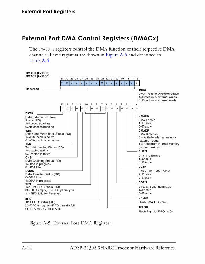
External Port Registers
A-14 ADSP-21368 SHARC Processor Hardware Reference
External Port DMA Control Registers (DMACx)The DMAC0–1 registers control the DMA function of their respective DMA channels. These registers are shown in Figure A-5 and described in Table A-4.
Figure A-5. External Port DMA Registers
15 14 13 12 11 10 9 8 7 6 5 4 3 2 1 0
DMAENEXTS
TLSTap List Loading Status (RO)1=Loading active0=Loading inactive
DMASDMA Transfer Status (RO)0=DMA idle1=DMA in progress
DMADRDMA Direction0 = Write to internal memory (external reads)1 = Read from Internal memory (external writes)
DMA Enable 1=Enable0=Disable
CHEN
Chaining Enable1=Enable0=Disable
DFSDMA FIFO Status (RO)00=FIFO empty, 01=FIFO partially full11=FIFO full, 10=Reserved
TFSTap List FIFO Status (RO)00=FIFO empty, 01=FIFO partially full11=FIFO full, 10=Reserved
DMAC0 (0x180B) DMAC1 (0x180C)
31 30 29 28 27 26 24 23 22 21 20 19 18 17 16
00 0 0 0 0 0 0 0 0 0 0 0 0 0 0
DIRSReserved
25
DLEN
Delay Line DMA Enable1=Enable0=Disable
CBEN
Circular Buffering Enable1=Enable0=Disable
DFLSH
Flush DMA FIFO (WO)
TFLSH
Flush Tap List FIFO (WO)
CHSDMA Chaining Status (RO)1=DMA in progress0=DMA Idle
DMA Transfer Direction Status 1=Direction is external writes0=Direction is external reads
00 0 0 0 0 0 0 0 0 0 0 0 0 0 0
WBSDelay Line Write Back Status (RO)1=Write back is active0=Write back is not active
DMA External Interface Status (RO)1=Access pending0=No access pending

ADSP-21368 SHARC Processor Hardware Reference A-15
Register Reference
Table A-4. External Port DMA Register Bit Descriptions
Bit Name Description
0 DMAEN DMA Enable.0 = External port channel x DMA is disabled1 = Enable External port DMA for channel x
1 DMADR DMA Direction0 = Write to internal memory (external reads)1 = Read from internal memory (external writes)Note: If delay line DMA is enabled then the DMADR bit doesn’t have any effect. For delay line DMA, transfer direction depends on the state of delay line transfers
2 CHEN Enable Chaining.0 = Chaining disabled1 = Chaining enabled
3 DLEN Enable Delay Line DMA. DLEN is applicable only if CHEN=1.0 = Delay-line DMA disabled1 = Delay-line DMA enabled
4 CBEN Circular Buffering Enable.0 = Disables circular buffering with delay line DMA1 = Enables circular buffering with delay line DMACircular Buffering can be used with normal DMA as well
5 DFLSH Flush DMA FIFO (write-only).
6 TFLSH Flush Tap List FIFO (write-only).
8–7 DFS DMA FIFO Status (read-only). 00 = FIFO empty01 = FIFO partially full11 = FIFO full10 = Reserved
10–9 TFS Tap List FIFO Status (read-only). 00 = FIFO empty01 = FIFO partially full11 = FIFO full10 = Reserved
11 DMAS DMA Transfer Status (read-only). 0 = DMA idle1 = DMA in progress

External Port Registers
A-16 ADSP-21368 SHARC Processor Hardware Reference
12 CHS DMA Chaining Status (read-only). 0 = DMA chain loading is not active1 = DMA chain loading is active
13 TLS Tap List Loading Status (read-only).0 = Tap list loading is not active1 = Tap list loading is active
14 WBS Delay Line Write Pointer Write Back Status (read-only).0 = Write pointer write back is not active1 = Write pointer write back is active
15 EXTS DMA External Interface Status (read-only).0 = DMA external interface does not have any access pending1 = DMA external interface has access pending
16 DIRS DMA Transfer Direction Status (read-only). 0 = DMA direction is external reads1 = DMA direction is external writesNote: This is useful for delay line DMA where the transfer direc-tion changes with the state of the DMA state machine.For normal DMA, DIRS will reflect the state of the DMADR bit.
31–17 Reserved
Table A-4. External Port DMA Register Bit Descriptions (Cont’d)
Bit Name Description
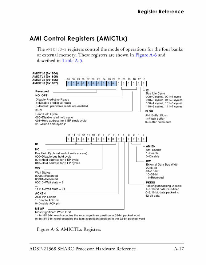
ADSP-21368 SHARC Processor Hardware Reference A-17
Register Reference
AMI Control Registers (AMICTLx)The AMICTL0–3 registers control the mode of operations for the four banks of external memory. These registers are shown in Figure A-6 and described in Table A-5.
Figure A-6. AMICTLx Registers
15 14 13 12 11 10 9 8 7 6 5 4 3 2 1 0
AMIENIC
HCBus Hold Cycle (at end of write access)000=Disable bus hold cycle001=Hold address for 1 EP cycle010=Hold address for 2 EP cycles
WSWait States00000=Reserved00001=Reserved00010=Wait state = 2...11111=Wait state = 31
BWExternal Data Bus Width00=8-bit01=16-bit10=32-bit11=Reserved
AMI Enable 1=Enable0=Disable
PKDISPacking/Unpacking Disable1=8/16-bit data zero-filled0=8/16 bit data packed to 32-bit data
MSWFMost Significant Word First1=1st 8/16-bit word occupies the most significant position in 32-bit packed word0=1st 8/16-bit word occupies the least significant position in the 32-bit packed word
ACKENACK Pin Enable1=Enable ACK pin0=Disable ACK pin
AMICTL0 (0x1804) AMICTL1 (0x1805)AMICTL2 (0x1806) AMICTL3 (0x1807)
31 30 29 28 27 26 24 23 22 21 20 19 18 17 16
00 0 0 0 0 0 0 0 0 0 0 0 0 0 0
RHCRead Hold Cycle000=Disable read hold cycle001=Hold address for 1 EP clock cycle010=Read hold cycle 2
ICBus Idle Cycle000=0 cycles, 001=1 cycle010=2 cycles, 011=3 cycles100=4 cycles, 101=5 cycles110=6 cycles, 111=7 cycles
NO_OPTDisable Predictive Reads 1=Disable predictive reads0=Default, predictive reads are enabled
FLSHAMI Buffer Flush1=Flush buffer0=Buffer holds data
Reserved
25
00 0 0 0 0 0 0 0 0 0 0 0 0 0 0

External Port Registers
A-18 ADSP-21368 SHARC Processor Hardware Reference
Table A-5. AMICTLx Register Bit Descriptions
Bit Name Description
0 AMIEN AMI Enable.0 = AMI is disabled1 = AMI is enabled
2–1 BW External Data Bus Width.00 = 8 bits01 = 16 bits10 = 32 bits11 = Reserved
3 PKDIS Disable Packing/Unpacking.0 = 8/16-bit data received packed to 32-bit data. Similarly, 32-bit data to be transmitted is unpacked to two 16-bit data or four 8-bit data.1 = 8/16-bit data received zero-filled, for transmitted data only 16-bit or the 8-bit LSB part of the 32-bit data is written to external memory.
4 MSWF Most Significant Word First. Applicable only with packing dis-abled (PKDIS=0).0 = 1st 8/16-bit word read/write occupies the least significant posi-tion in the 32-bit packed word.1 = 1st 8/16-bit word read/write occupies the most significant posi-tion in the 32-bit packed word.
5 ACKEN Enable the ACK pin.If enabled, reads/writes to devices have to be extended by the corre-sponding devices by pulling ACK low. When ACKEN is set then the ACK pin is sampled after the waitstate value is programmed.
10–6 WS Wait States.00000 = Reserved (wait state value of 32 if used)00001 = Reserved for internal use (can be used when the clock fre-quencies are low)00010 = wait state = 2 external port clock cycles...11111 = Wait state = 31 external port clock cycles
13–11 HC Bus Hold Cycle at the End of Write Access.000 = Disable bus hold cycle001 = Hold address for one external port clock cycle010 = Hold address for two external port clock cycles

ADSP-21368 SHARC Processor Hardware Reference A-19
Register Reference
16–14 IC Bus Idle Cycle. Idle cycle to be inserted whenever read from exter-nal memory is followed by a write to external memory – to avoid contention. 'IC' EP clock cycles are ensured between a read to write.000 = 0 cycles, 001 = 1 cycle010 = 2 cycles, 011 = 3 cycles100 = 4 cycles, 101 = 5 cycles110 = 6 cycles, 111 = 7 cycles
17 FLSH AMI Buffer Flush (Write-only).0 = Buffer holds the data1 = Flush the buffer
20–18 RHC Read Hold Cycle at the End of Read Access. Controls the delay between two reads.000 = Disable read hold cycle001 = Hold address for one external port clock cycle010 = Hold address for two external port clock cycles
21 NO_OPT Disable Predictive Reads.Default is predictive reads are enabled. For more information, see “SDRAM Read Optimization” on page 3-75.
31–22 Reserved
Table A-5. AMICTLx Register Bit Descriptions (Cont’d)
Bit Name Description

External Port Registers
A-20 ADSP-21368 SHARC Processor Hardware Reference
AMI Status Register (AMISTAT)This 32-bit, read-only register provides status information for the AMI interface and can be read at any time. This register is shown in Figure A-7.
Figure A-7. AMISTAT Register
15 14 13 12 11 10 9 8 7 6 5 4 3 2 1 0
00 0 0 0 0 0 0 0 0 0 0 0 0 0 0
AMIMS
AMIRXSAMI External Receive Register (AMIRX) Status 1=Receive register has valid data0=Receive register empty
Reserved (Bits 31–4)
AMI External Transmit Register (AMITX) Status1=Transmit register has valid data0=Transmit register empty
AMI Master1=AMI controls the external pins0=SDC controls the exter-nal pins
AMISExternal Interface Status1=AMI access pending0=AMI interface idle
AMITXS
AMISTAT (0x180A)

ADSP-21368 SHARC Processor Hardware Reference A-21
Register Reference
SDRAM Control Register (SDCTL)The SDRAM memory control register includes all programmable parame-ters associated with the SDRAM access timing and configuration. This 32-bit register is located at address 0x1800 and is shown in Figure A-8 and described in Table A-6. For more information, see “SDRAM Control Register (SDCTL)” on page 3-39.
Figure A-8. SDRAM Control Register (Bits 16–31)
31 30 29 28 27 26 24 23 22 21 20 19 18 17 16
00 0 0 0 0 0 0 0 0 0 0 0 0 0 0
SDBUF
Row Address Width000=8, 001=9010=10, 011=11100=12, 101=13110=14, 111=15
X16DESDRAM External Data Path Width(ADSP-21371 only)1=16 bits0=32 bits
SDRAW
SDRAM tRCD SpecificationtRCD = 1–7 SDCLK cycles
SDTWRSDRAM tWR Specification tWR = 1–3 SDCLK cycles
NO BSTOP
25
SDORF
Pipeline Option with External Register Buffer1=External SDRAM CTL/ADDR control buffer enable0=No buffer option
Force AR
Optional Refresh1=Auto refresh not performed0=Auto refresh occurs when refresh counter expires
Force Auto Refresh1=Force auto refresh0=No effectForce PCForce Precharge1=Force precharge0=No effect
STDRCD
Force LMR
SDCTL (0x1800)
Disable 1=Disable burst stop0=Issue burst stop on a read/write break
PGSZ 128Disable 1=Page size is 128 words (Col width = 7 bits)0=No effect
Force Auto Refresh1=Force mode register write0=No effect

External Port Registers
A-22 ADSP-21368 SHARC Processor Hardware Reference
Figure A-9. SDRAM Control Register (Bits 0–15)
Table A-6. SDRAM Control Register Bit Descriptions
Bit Name Description
1–0 SDCL SDRAM CAS Latency. The delay in clock cycles between when the SDRAM detects the read command and when it provides the data at its output pins.00, 01 = Reserved10 = 2 cycles11 = 3 cycles
2 DSDCTL Disable SDCLK and Control Signals. Used to enable or disable the SDC. If DSDCTL is disabled, any access to SDRAM address space does not occur externally. When DSDCTL is disabled, all SDC control pins are in their inactive states and the SDRAM clock SDCLK is not running.1 = Disable0 = Activate
3 Reserved.
15 14 13 12 11 10 9 8 7 6 5 4 3 2 1 0
SDCLSDSRFSDRAM Self Refresh Enable1=Starts self refresh mode0=No effectSDPSSSDRAM Power-up Sequence Start1=Enable power-up on next SDRAM access0=No effect
DSDCTLDisable SDCLK and Control Sig-nals1=Disable0=Activate
CAS Latency00, 01=Reserved10=2 cycles, 11=3 cycles
Reserved
SDPMSDRAM Power-Up Mode1=Precharge, mode reg set, 8CBR refresh cycles0=Precharge, 8CBR refresh cycles, mode reg set
SDCAWSDRAM Bank Column Address Width00=8 bits01=9 bits10=10 bits11=11 bits
00 0 0 0 0 0 0 0 0 0 0 0 0 0 0
SDTRASSDRAM tRAS SpecificationActive command delay = 1–15 SDCLK cyclesSDTRPSDRAM tRP SpecificationPrecharge delay = 1–7 SDCLK cycles
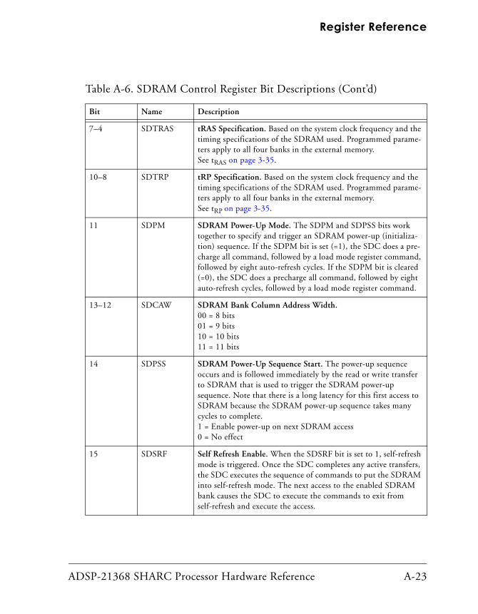
ADSP-21368 SHARC Processor Hardware Reference A-23
Register Reference
7–4 SDTRAS tRAS Specification. Based on the system clock frequency and the timing specifications of the SDRAM used. Programmed parame-ters apply to all four banks in the external memory.See tRAS on page 3-35.
10–8 SDTRP tRP Specification. Based on the system clock frequency and the timing specifications of the SDRAM used. Programmed parame-ters apply to all four banks in the external memory.See tRP on page 3-35.
11 SDPM SDRAM Power-Up Mode. The SDPM and SDPSS bits work together to specify and trigger an SDRAM power-up (initializa-tion) sequence. If the SDPM bit is set (=1), the SDC does a pre-charge all command, followed by a load mode register command, followed by eight auto-refresh cycles. If the SDPM bit is cleared (=0), the SDC does a precharge all command, followed by eight auto-refresh cycles, followed by a load mode register command.
13–12 SDCAW SDRAM Bank Column Address Width.00 = 8 bits01 = 9 bits10 = 10 bits11 = 11 bits
14 SDPSS SDRAM Power-Up Sequence Start. The power-up sequence occurs and is followed immediately by the read or write transfer to SDRAM that is used to trigger the SDRAM power-up sequence. Note that there is a long latency for this first access to SDRAM because the SDRAM power-up sequence takes many cycles to complete.1 = Enable power-up on next SDRAM access0 = No effect
15 SDSRF Self Refresh Enable. When the SDSRF bit is set to 1, self-refresh mode is triggered. Once the SDC completes any active transfers, the SDC executes the sequence of commands to put the SDRAM into self-refresh mode. The next access to the enabled SDRAM bank causes the SDC to execute the commands to exit from self-refresh and execute the access.
Table A-6. SDRAM Control Register Bit Descriptions (Cont’d)
Bit Name Description

External Port Registers
A-24 ADSP-21368 SHARC Processor Hardware Reference
16 X16DE SDRAM External Data Path Width. Selects whether the SDRAM interface is 32 or 16 bits wide. If X16DE = 0, DATA31–0 should be connected to the SDRAM. If X16DE = 1, DATA15–0 should be connected to the SDRAM and 16 to 32-bit packing is performed. (Valid for all processors except for the ADSP-21375 processor).
18–17 SDTWR SDRAM tWR Specification. tWR = 1–3 SDCLK cycles. Based on the system clock frequency and the timing specifications of the SDRAM used. Programmed parameters apply to all four banks in the external memory.See tWR on page 3-35.
19 SDORF Optional Refresh.1 = Auto refresh not performed0 = Auto refresh occurs when refresh counter expires(see “Auto-Refresh” on page 3-70).
20 Force AR Force Auto Refresh.1 = Force auto refresh0 = No effect
21 Force PC Force Precharge.1 = Force precharge0 = No effect
22 Force LMR Force Load Mode Register Write. This command performs a load mode register command immediately. This is in contrast to the normal load mode register set which requires some delay. This command performs a precharge all (if not precharged already) followed by a mode register write. (Valid for ADSP-2137x pro-cessors only).
23 SDBUF Pipeline Option with External Register Buffer.1 = External SDRAM CTL/ADDR control buffer enable0 = No buffer option
26–24 SDTRCD SDRAM tRCD Specification. tRCD = 1–7 SDCLK cycles. Based on the system clock frequency and the timing specifications of the SDRAM used. Programmed parameters apply to all four banks in the external memory.See tRCD on page 3-35.
Table A-6. SDRAM Control Register Bit Descriptions (Cont’d)
Bit Name Description

ADSP-21368 SHARC Processor Hardware Reference A-25
Register Reference
29–27 SDRAW Row Address Width.000=8, 001=9010=10, 011=11100=12, 101=13110=14, 111=15
30 PGSZ 128 Program the SDRAM Controller for Page Size of 128 Words.This bit allows programs to configure the SDC for a page size of 128 words (7 bits) which supports most available 32 Mb SDRAMs.1 = Page size 128 words. Column width = 7 bits, override CAW settings.0 = No effect, page size decided by SDCAW bits.(Valid for ADSP-2137x processors only).
31 NO BSTOP No Burst Mode. This bit is used to select between full page burst or no burst mode (BL=1). If set (=1), no burst mode is active and the burst stop command is ignored. If cleared, full page burst is active using the burst stop command for access interruption. This bit must be cleared if the SDRAM does not support no burst mode but supports full page burst. (Valid for ADSP-2137x processors only).
Table A-6. SDRAM Control Register Bit Descriptions (Cont’d)
Bit Name Description

External Port Registers
A-26 ADSP-21368 SHARC Processor Hardware Reference
SDRAM Control Status Register (SDSTAT)The SDRAM control status register provides information on the state of the SDC. This information can be used to determine when it is safe to alter SDC control parameters or as a debug aid. This register is located at address 0x1803 and is shown in Figure A-10.
SDRAM Refresh Rate Control Register (SDRRC)The SDRAM refresh rate control register provides a flexible mechanism for specifying the auto-refresh timing. The SDC provides a programmable refresh counter which has a period based on the value programmed into the RDIV field of this register, that coordinates the supplied clock rate with the SDRAM device’s required refresh rate. This register is located at address 0x1802 and is shown in Figure A-11. For more information, see “SDRAM Refresh Rate Control Register (SDRRC)” on page 3-49 and for information on using the SMODIFY bit see “SDRAM Read Optimization” on page 3-75.
Figure A-10. SDRAM Control Status Register
15 14 13 12 11 10 8 7 6 5 4 3 2 1 0
00 0 0 0 0 0 0 0 0 0 0 0 1 0 0
Reserved
SDPUA
SDCI
SDRAM Controller Idle1=SDC is idle0=SDC busy is busy in per-forming an access or auto-refreshSDSRA
SDRAM Self-Refresh Active1=In self-refresh mode0=Not in self-refresh mode
SDRAM Power-Up Active1=SDC in power-up sequence0=SDC not in power-up sequence
SDRSSDRAMs In Reset State1=No power-up sequence has been initiated since last SDC reset0=Power-up sequence has been initiated since last SDC reset
9SDSTAT (0x1803)

ADSP-21368 SHARC Processor Hardware Reference A-27
Register Reference
Figure A-11. SDRAM Control Refresh Rate Register
15 14 13 12 11 10 8 7 6 5 4 3 2 1 0
00 0 0 0 0 0 0 0 0 0 0 1 1 0 10
Reserved RDIVDelay (SDCLK cycles) between consecutive refresh counter time-outs
SDROPT
SDRAM Optimization1=Enable0=Disable
SDMODIFY
Used for Predictive Addressing (0–15)
9
SDRRC (0x1802) 31 30 29 28 27 26 24 23 22 21 20 19 18 17 16
10 0 0 0 0 0 0 0 0 0 0 0 0 0 1
25
Reserved

Memory-to-Memory DMA Register
A-28 ADSP-21368 SHARC Processor Hardware Reference
Memory-to-Memory DMA RegisterThe memory-to-memory (MTM) DMA register (MTMCTL) allows programs to transfer blocks of 64-bit data from one internal memory location to another. This transfer method uses two DMA channels, one for reading data and one for writing data. These transfers are controlled using the MTMCTL register shown in Figure A-12. For more information, see “Mem-ory-to-Memory DMA” on page 2-48.
Figure A-12. MTM DMA Register (MTMCTL)
31 30 29 28 27 26 24 23 22 21 20 19 18 17 16
00 0 0 0 0 0 0 0 0 0 0 0 0 0 0
Read of bits 29–4 returns 0
15 14 13 12 11 10 8 7 6 5 4 3 2 1 0
00 0 0 0 1 1 1 1 0 0 0 0 0 0 0
MTMDMA0ACT
MTMDENMTM DMA Enable1=Enable0=Disable
Reserved
Memory Write DMA Status
MTMFLUSH1=Flush the FIFO and reset the read/write pointers
24
9
MTMCTL (0x2C01)
MTMDMA1ACT
Memory Read DMA Status

ADSP-21368 SHARC Processor Hardware Reference A-29
Register Reference
Serial Port RegistersThe following section describes serial port (SPORT) registers.
SPORT Serial Control Registers (SPCTLx)The SPORT serial control registers’ addresses are:
The reset value for these registers is 0x0000 0000. The SPCTLx registers are transmit and receive control registers for the corresponding serial ports (SPORT 0 through 7). The following figures show the bit descriptions and settings for the SPORT operating modes.
• Figure A-13 and Figure A-14 provide bit definitions for standard DSP serial mode.
• Figure A-15 provides bit definitions in left-justified sample-pair and I2S mode.
• Figure A-16, Figure A-17 and Figure A-18 provide bit definitions for packed I2S and multichannel mode.
When changing SPORT operating modes, programs should clear the serial port’s control register before writing the new settings to the control register. See Table A-7 for a complete description of SPORT operation modes and Table A-8 for complete bit descriptions.
SPCTL0 – 0xC00 SPCTL1 – 0xC01
SPCTL2 – 0x400 SPCTL3 – 0x401
SPCTL4 – 0x800 SPCTL5 – 0x801
SPCTL6 – 0x4800 SPCTL7 – 0x4801

Serial Port Registers
A-30 ADSP-21368 SHARC Processor Hardware Reference
Table A-7. SPORT Operation Modes
Operating Modes
Bits
OPMODE LAFS FRFS MCEA MCEB SLENx
Standard DSP Serial Mode 0 0, 1 X 0 0 3-321
I2S (Tx/Rx on Left Channel First)
1 0 1 0 0 8-32
I2S (Tx/Rx on Right Channel First)
1 0 0 0 0 8-32
Packed I2S Mode A Channel 1 0 X 1 0 3-32
Packed I2S Mode B Channel 1 0 X 0 1 3-32
Packed I2S Mode A and B Channels
1 0 X 1 1 3-32
Left-Justified Sample Pair Mode (Tx/Rx on FS Rising Edge)
1 1 0 0 0 8-32
Left-Justified Sample Pair (Tx/Rx on FS Falling Edge)
1 1 1 0 0 8-32
Multichannel A Channels 0 0 X 1 0 3-321
Multichannel B Channels 0 0 X 0 1 3-321
Multichannel A and B Channels
0 0 X 1 1 3-321
1 Although serial ports process word lengths of 3 to 32 bits, transmitting or receiving words small-er than 7 bits at core clock frequency/4 of the processor may cause incorrect operation when DMA chaining is enabled. Chaining disables the processor’s internal I/O bus for several cycles while the new transfer control block (TCB) parameters are being loaded. Receive data may be lost (for example, overwritten) during this period.

ADSP-21368 SHARC Processor Hardware Reference A-31
Register Reference
Figure A-13. SPCTLx Register (Bits 16–31) for Standard DSP Serial Mode
31 30 29 28 27 26 24 23 22 21 20 19 18 17 16
00 0 0 0 0 0 0 0 0 0 0 0 0 0 0
DXS_AData Buffer Channel A Status11=Full, 10=Partially Full, 00=Empty
LFSActive Low Frame Sync1=Active low0=Active highDERR_A
Channel A Error Status (sticky)SPTRAN=1 Transmit underflow status SPTRAN=0 Receive overflow status
SDEN_ADMA Channel A Enable1=Enable0=Disable
DXS_BData Buffer Channel B Status11=Full, 10=Partially Full, 00=Empty
DERR_BChannel B Error Status (sticky)SPTRAN=1 Transmit underflow statusSPTRAN=0 Receive overflow status
SPTRANSPORT Data Direction1=Transmit0=Receive
SPEN_BSPORT Enable B1=Enable0=Disable
BHDBuffer Hang Disable1=Ignore core hang0=Core stall when TXSPx full or RXSPx empty
LAFSLate Frame Sync1=Late frame sync0=Early frame sync
SCHEN_ADMA Channel A Chaining Enable1=Enable0=Disable
SDEN_BDMA Channel B Enable1=Enable0=Disable
SCHEN_BDMA Channel B Chaining Enable1=Enable0=Disable
25
FS_BOTH
Frame Sync Both1=Issue word select if data is present in both TXSPxy and RXSPxy0=Issue word select if data is present in either of TXSPxy or RXSPxy buffers
SPCTL0 (0xC00) SPCTL1 (0xC01)SPCTL2 (0x400) SPCTL3 (0x401)SPCTL4 (0x800) SPCTL5 (0x800)SPCTL6 (0x4800) SPCTL7 (0x4801)

Serial Port Registers
A-32 ADSP-21368 SHARC Processor Hardware Reference
Figure A-14. SPCTLx Register (Bits 0–15) for Standard DSP Serial Mode
15 14 13 12 11 10 9 8 7 6 5 4 3 2 1 0
00 0 0 0 0 0 0 0 0 0 0 0 0 0 0
SPEN_ADIFSData Independent TX FS (if SPTRAN=1) or RX FS (if SPTRAN=0) 1=Data independent0=Data dependent
IFSInternally-Generated FS1=Internal0=External
FSRFrame Sync Requirement1=Frame sync required0=Frame sync not required
CKREClock Edge for Data Frame Sync Sampling or Driving1=Rising edge0=Falling edge
OP MODESPORT Operation Mode0=DSP serial mode/multichannel mode,this bit must be set to 0
DTYPEData Type00=Right-justify01=Right-justify, sign extend MS10=Compand mu-law11=Compand A-law
ICLKInternally-Generated SPORTx_CLK1=Internal clock0=External clock
SPORT Enable A1=Enable0=Disable
LSBFLeast Significant Bit Format1=LSB first0=MSB first
SLENSerial Word Length=1
PACK16/32 Packing1=Packing0=No packing
SPCTL0 (0xC00) SPCTL1 (0xC01)SPCTL2 (0x400) SPCTL3 (0x401)SPCTL4 (0x800) SPCTL5 (0x801)SPCTL6 (0x4800) SPCTL7 (0x4801)

ADSP-21368 SHARC Processor Hardware Reference A-33
Register Reference
Figure A-15. SPCTLx Register (Bits 31–16) for I2S and Left-Justified Sample Pair Modes
31 30 29 28 27 26 24 23 22 21 20 19 18 17 16
00 0 0 0 0 0 0 0 0 1 0 0 0 0 0
DXS_AData Buffer Channel A Status11=Full, 10=Partially Full, 00=Empty
FRFSSee Table 5-1 on page 5-11
DERR_AChannel A Error Status (Sticky)SPTRAN=1 Transmit underflow status SPTRAN=0 Receive overflow status
SDEN_ADMA Channel A Enable1=Enable0=Disable
DXS_BData Buffer Channel B Status11=Full, 10=Partially Full, 00=Empty
DERR_BChannel B Error Status (Sticky)SPTRAN=1 Transmit underflow statusSPTRAN=0 Receive overflow status
SPTRANSPORT Transaction1=Active transmit buffers TXSPXA/TXSPXB0=Enable receive buffers RXSPXA/RXSPXBSPEN_BSPORT Enable B1=Enable0=Disable BHD
Buffer Hang Disable1=Ignore core hang0=Core stall when TXSPx Full or RXSPx empty
LAFSLate Frame Sync
SCHEN_ADMA Channel A Chaining Enable1=Enable0=DisableSDEN_BDMA Channel B Enable1=Enable0=Disable
SCHEN_BDMA Channel B Chaining Enable1=Enable0=DisableReserved
25
SPCTL0 (0xC00) SPCTL1 (0xC01)SPCTL2 (0x400) SPCTL3 (0x401)SPCTL4 (0x800) SPCTL5 (0x801)SPCTL6 (0x4800) SPCTL7 (0x4801)
Serial Port Registers
A-34 ADSP-21368 SHARC Processor Hardware Reference
Figure A-16. SPCTLx Register (Bits 15 – 0) for I2S and Left-Justified Sample Pair Modes
SPCTL0 (0xC00) SPCTL1 (0xC01)SPCTL2 (0x400) SPCTL3 (0x401)SPCTL4 (0x800) SPCTL5 (0x801)SPCTL6 (0x4800) SPCTL7 (0x4801)
15 14 13 12 11 10 9 8 7 6 5 4 3 2 1 0
00 0 0 0 0 0 0 0 0 0 0 0 0 0 0
SPEN_ADIFSData Independent Frame Sync 1=Data independent0=Data dependent
ReservedOP MODESPORT Operation Mode1=I2S or left-justified sample pair mode, this bit must be set to 1
MSTRI2S Serial and L/R Clock Master21=Internal clock and word select0=External clock and word select
SPORT Enable A1=Enable0=Disable
ReservedSLENSerial word length=1
PACK16/32 Packing1=Packing0=No packing

ADSP-21368 SHARC Processor Hardware Reference A-35
Register Reference
Figure A-17. SPCTLx Register (Bits 31–16) for Packed I2S and Multichannel Mode
31 30 29 28 27 26 24 23 22 21 20 19 18 17 16
00 0 0 0 0 0 0 0 0 0 0 0 0 0 0
DXS_AData Buffer Channel A Status11=Full 10=Partially full 00=Empty
LMFSActive Low Multichannel Frame Sync1=Active low FS0=Active high FS
DERR_A (TUVF_A or ROVF_A)Channel A Error Status (sticky) SPTRAN=1 Transmit underflow status SPTRAN=0 Receive overflow status
SDEN_AReceive DMA Channel A Enable1=Enable0=Disable
DXS_BData Buffer Channel B Status11=Full 10=Partially full 00=Empty
BHDBuffer Hang Disable1=Ignore core hang0=Core stall when TXn full or RXn empty
SCHEN_AReceive DMA Channel A Chaining Enable1=Enable0=Disable
SDEN_BReceive DMA Channel B Enable1=Enable0=DisableSCHEN_BReceive DMA Channel B Chaining Enable1=Enable0=Disable
Reserved
Reserved
25
SPTRANSPORT Data Direction 1=Transmit0=Receive
SPCTL0 (0xC00) SPCTL1 (0xC01)SPCTL2 (0x400) SPCTL3 (0x401)SPCTL4 (0x800) SPCTL5 (0x801)SPCTL6 (0x4800) SPCTL7 (0x4801)
DERR_B (TUVF_B or ROVF_B)Channel B Error Status (sticky) SPTRAN=1 Transmit underflow status SPTRAN=0 Receive overflow status
Reserved

Serial Port Registers
A-36 ADSP-21368 SHARC Processor Hardware Reference
Figure A-18. SPCTLx Register (Bits 15–0) for Packed I2S and Multichannel Mode
15 14 13 12 11 10 9 8 7 6 5 4 3 2 1 0
00 0 0 0 0 0 0 0 0 0 0 0 0 0 0
Reserved Reserved
IMFS DTYPEData Type00=Right-justify, fill MSB with 0’s01=Right-justify, sign-extend MSB10=Compand υ-law11=Compand A-lawLSBFSerial Word Bit Order1=LSB first0=MSB first
SLENSerial Word Length-1
PACK16/32 Packing1=Packing0=No packing
Internally Generated Multichannel Frame Sync1=Internal frame sync0=External frame sync
OPMODESPORT Operation Mode1=Packed I2S mode0=Multichannel mode
CKREActive Clock Edge for Data and Frame Sync Sampling1=Rising edge0=Falling edge
Reserved
ICLKInternally Generated Clock1=Internal clock0=External clock
SPCTL0 (0xC00) SPCTL1 (0xC01)SPCTL2 (0x400) SPCTL3 (0x401)SPCTL4 (0x800) SPCTL5 (0x801)SPCTL6 (0x4800) SPCTL7 (0x4801)

ADSP-21368 SHARC Processor Hardware Reference A-37
Register Reference
Table A-8. SPCTLx Register Bit Descriptions
Bit Name Description
0 SPEN_A Enable Channel A Serial Port. 0 = Serial port A channel disabled1 = Serial port A channel enabledThis bit is reserved when the SPORT is in packed I2S and multichan-nel modes.
2–1 DTYPE Data Type Select. Selects the data type formatting for normal and multichannel transmissions as follows:Normal Multichannel Data Type Formatting00 x0 Right-justify, zero-fill unused MSBs 01 x1 Right-justify, sign-extend unused MSBs 10 0x Compand using μ-law 11 1x Compand using A-law
3 LSBF Serial Word Endian Select. 0 = Big endian (MSB first)1 = Little endian (LSB first)This bit is reserved when the SPORT is in I2S or left-justified sample pair modes.
8–4 SLEN Serial Word Length Select. Selects the word length in bits. For DSP serial and multichannel modes, word sizes can be from 3 bits (SLEN = 2) to 32 bits (SLEN = 31). For I2S and left-justified modes, word sizes can be from 8 bits (SLEN = 7) to 32 bits (SLEN = 31).
9 PACK 16-Bit to 32-Bit Word Packing Enable. 0 = Disable 16- to 32-bit word packing1 = Enable 16- to 32-bit word packing
10 ICLK Internal Clock Select.0 = Select external transmit clock 1 = Select the internal transmit clockThis bit applies to DSP serial and multichannel modes, including packed I2S modes.
MSTR (I2S mode only)
In I2S and left-justified sample pair mode, this bit selects the word source and internal clock (if set, = 1) or external clock (if cleared, = 0)
11 OPMODE Sport Operation Mode.0 = DSP serial/multichannel mode if cleared1 = Selects the I2S, packed I2S, left-justified sample pair mode

Serial Port Registers
A-38 ADSP-21368 SHARC Processor Hardware Reference
12 CKRE Clock Rising Edge Select. Determines clock signal to sample data and the frame sync selection.0 = Falling edge1 = Rising edgeCKRE is reserved when the SPORT is in I2S and left-justified sample pair modes.
13 FSR Frame Sync Required Select. Selects whether the serial port requires (if set, = 1) or does not require a transfer frame sync (if cleared, = 0). FSR is reserved when the SPORT is in packed I2S, I2S, left-justified sample pair, and multichannel modes. See Table A-7 on page A-30.
14 IFS(IMFS)
Internal Frame Sync Select. Selects whether the serial port uses an internally-generated frame sync (if set, = 1) or uses an external frame sync (if cleared, = 0). This bit is reserved when the SPORT is in I2S mode, left-justified sample pair mode. See Table A-7 on page A-30.
15 DIFS Data Independent Frame Sync Select. 1 = Serial port uses a data-independent frame sync (sync at selected interval)0 = Serial port uses a data-dependent frame sync (sync when TX FIFO is not empty or when RX FIFO is not full). This bit is reserved when the SPORT is in packed I2S and multichannel modes. See Table A-7 on page A-30.
16 LFS, FRFS, LMFS
Active Low Frame Sync Select. Depending on the OPMODE, selects an active high or low, left or right channel frame sync. See Table A-7 on page A-30.
17 LAFS Late Transmit Frame Sync Select. 0 = Early frame sync (FS before first bit). 1 = Late frame sync (FS during first bit) This bit is reserved when the SPORT is in packed I2S and multichan-nel modes. See Table A-7 on page A-30.
18 SDEN_A Enable Channel A Serial Port DMA. 0 = Disable serial port channel A DMA1 = Enable serial port channel A DMA
19 SCHEN_A Enable Channel A Serial Port DMA Chaining. 0 = Disable serial port channel A DMA chaining1 = Enable serial port channel A DMA chaining
Table A-8. SPCTLx Register Bit Descriptions (Cont’d)
Bit Name Description

ADSP-21368 SHARC Processor Hardware Reference A-39
Register Reference
20 SDEN_B Enable Channel B Serial Port DMA. 0 = Disable serial port channel B DMA1 = Enable serial port channel B DMA
21 SCHEN_B Enable Channel B Serial Port DMA Chaining.0 = Disable serial port channel B DMA chaining1 = Enable serial port channel B DMA chaining
22 FS_BOTH FS Both Enable. 0 = Issue WS if data is present in either transmit buffer1 = Issue WS if data is present in both transmit buffersThis bit is reserved when the SPORT is in packed I2S, multichannel, I2S and left-justified sample pair modes.
23 BHD Buffer Hang Disable. 0 = Indicates a core stall. The core stalls when it tries to write to a full transmit buffer or read an empty receive buffer FIFO.1 = Ignore a core hangThis bit applies to all modes.
24 SPEN_B Enable Channel B Serial Port.0 = Serial port A channel disabled1 = Serial port A channel enabledThis bit is reserved when the SPORT is in packed I2S and multichan-nel modes.
25 SPTRAN Data Direction Control. 0 = Enable receive buffers 1 = Activate transmit buffers
26 DERR_B (TUVF_B or ROVF_B)
Channel B Error Status (sticky, read-only). Indicates if the serial transmit operation has underflowed or a receive operation has over-flowed in the channel B data buffer.
28–27 DXS_B Channel B Data Buffer Status (read-only). Indicates the status of the serial port’s channel B data buffer as follows: 11 = Full00 = Empty10 = Partially full This bit is reserved when the SPORT is in multichannel mode.
Table A-8. SPCTLx Register Bit Descriptions (Cont’d)
Bit Name Description

Serial Port Registers
A-40 ADSP-21368 SHARC Processor Hardware Reference
SPORT Multichannel Control Registers (SPMCTLx) Unlike previous SHARC designs, the serial ports in the ADSP-21367/8/9 and ADSP-2137x processors work individually, not in pairs. Therefore, each SPORT has its own multichannel control register. These registers are shown in Figure A-19 and described in Table A-9. The reset value for these registers is undefined and their addresses are:
29 DERR_A (TUVF_A or ROVF_A)
Channel A Error Status (sticky, read-only). Indicates if the serial transmit operation has underflowed or a receive operation has over-flowed in the channel A data buffer.
31–30 DXS_A Channel A Data Buffer Status (read-only). Indicates the status of the 11 = Full00 = Empty10 = Partially full
SPMCTL0 – 0xC04
SPMCTL1 – 0xC17
SPMCTL2 – 0x404
SPMCTL3 – 0x417
SPMCTL4 – 0x804
SPMCTL5 – 0x817
SPMCTL6 – 0x4804
SPMCTL7 – 0x4817
Table A-8. SPCTLx Register Bit Descriptions (Cont’d)
Bit Name Description

ADSP-21368 SHARC Processor Hardware Reference A-41
Register Reference
Figure A-19. SPMCTLx Registers – Multichannel Mode
31 30 29 28 27 26 24 23 22 21 20 19 18 17 16
00 0 0 0 0 0 0 0 0 0 0 0 0 0 0
DMACHSxBSPORTx Channel B StatusDMA Chaining Status x = 0,2,4,6
CHNLCurrent Channel Status (read-only)
DMASxASPORTx Channel A DMA status x = 0,2,4,6
MCEBMultichannel EnableB Channels0=Disable1=Enable
DMACHSxASPORTx Channel A StatusDMA Chaining Status x = 0,2,4,6
DMACHSyBSPORTx Channel B StatusDMA Chaining Status y = 1,3,5,7
DMACHSyASPORTx Channel A StatusDMA Chaining Status y = 1,3,5,7
DMASyBSPORTx Channel B DMA Status y = 1,3,5,7
DMASyASPORTx Channel A DMA Status y = 1,3,5,7
DMASxBSPORTx Channel B DMA status x = 0,2,4,6
15 14 13 12 11 10 8 7 6 5 4 3 2 1 0
00 0 0 0 0 0 0 0 0 0 0 0 0 0 0
ReservedSPL
MCEAMultichannel Enable A Channels1=Enable0=Disable
MFDxMultichannel Frame Delay
SPORT LoopbackSPORT0 A to SPORT1 A onlySPORT0 B to SPORT1 B only
NCHNumber of Channels – 1
25
9
SPMCTL0 (0xC04) SPMCTL1 (0xC17)SPMCTL2 (0x404) SPMCTL3 (0x417)SPMCTL4 (0x804) SPMCTL5 (0x817)SPMCTL6 (0x4804) SPMCTL7 (0x4817)

Serial Port Registers
A-42 ADSP-21368 SHARC Processor Hardware Reference
Table A-9. SPMCTLx Register Bit Descriptions
Bit Name Description
0 MCEA Multichannel Mode Enable. Standard and multichannel modes only. One of two configuration bits that enable and disable mul-tichannel mode on serial port channels. See OPMODE bit on page A-37.0 = Disable multichannel operation1 = Enable multichannel operation if OPMODE = 0
4–1 MFD Multichannel Frame Delay. Set the interval, in number of serial clock cycles, between the multichannel frame sync pulse and the first data bit. These bits provide support for different types of T1 interface devices. Valid values range from 0 to 15 with bits [4:1]. Values of 1 to15 correspond to the number of intervening serial clock cycles. A value of 0 corresponds to no delay. The multi-channel frame sync pulse is concurrent with first data bit.
11–5 NCH Number of Multichannel Slots (minus one). Select the number of channel slots (maximum of 128) to use for multichannel oper-ation. Valid values for actual number of channel slots range from 1 to 128. Use this formula to calculate the value for NCH: NCH = Actual number of channel slots – 1.
12 SPL SPORT Loopback Mode. Enables if set (= 1) or disables if cleared (= 0) the channel loopback mode. Loopback mode enables developers to run internal tests and to debug applications. Loopback works under the following SPORT configurations where either of the two paired SPORTs can be set up to transmit or receive, depending on their SPTRAN bit setting.
SPORT0 and SPORT1. SPORT0 can only be paired with SPORT1, controlled by the SPL bit in the SPMCTL0 register.
SPORT2 and SPORT3. SPORT2 can only be paired with SPORT3, controlled by the SPL bit in the SPMCTL2 register.
SPORT4 and SPORT5. SPORT4 can only be paired with SPORT5, controlled by the SPL bit in the SPMCTL4 register.
SPORT6 and SPORT7. SPORT6 can only be paired with SPORT7, controlled via SPL bit in the SPMCTL6 register
15–13 Reserved

ADSP-21368 SHARC Processor Hardware Reference A-43
Register Reference
SPORT Transmit Buffer Registers (TXSPx)The addresses of the TXSPx registers are:
The 32-bit TXSPx registers hold the output data for serial port transmit operations. The reset value for these registers is undefined. For more information on how transmit buffers work, see “Transmit and Receive Data Buffers (TXSPxA/B, RXSPxA/B)” on page 5-67.
22–16 CHNL Current Channel Selected (read-only, sticky). Identify the cur-rently selected transmit channel slot (0 to 127).
23 MCEB Multichannel Enable, B Channels.0 = Disable1 = Enable
27–24 DMASxy DMA Status. Selects the transfer status.0 = Inactive1 = Active (read-only)
31–28 DMACHSxy DMA Chaining Status.0 = Inactive1 = Active(read-only)
TXSP0A – 0xC60 TXSP0B – 0xC62
TXSP1A – 0xC64 TXSP1B – 0xC66
TXSP2A – 0x460 TXSP2B – 0x462
TXSP3A – 0x464 TXSP3B – 0x466
TXSP4A – 0x860 TXSP4B – 0x862
TXSP5A – 0x864 TXSP5B – 0x866
TXSP6A – 0x4860 TXSP6B – 0x4862
TXSP7A – 0x4864 TXSP7B – 0x4866
Table A-9. SPMCTLx Register Bit Descriptions (Cont’d)
Bit Name Description
Serial Port Registers
A-44 ADSP-21368 SHARC Processor Hardware Reference
SPORT Receive Buffer Registers (RXSPx)The 32-bit RXSPx registers hold the input data from serial port receive operations. The reset value for these registers is undefined. For more information on how receive buffers work, see “Transmit and Receive Data Buffers (TXSPxA/B, RXSPxA/B)” on page 5-67. The addresses of the RXSPx registers are:
SPORT Divisor Registers (DIVx)The addresses of the DIVx registers are:
These registers, shown in Figure A-20, have an undefined reset value. These registers contain two fields:
• Bits 15–1 are CLKDIV. These bits identify the serial clock divisor value for internally-generated SCLK as follows:
RXSP0A – 0xc61 RXSP0B – 0xc63
RXSP1A – 0xc65 RXSP1B – 0xc67
RXSP2A – 0x461 RXSP2B – 0x463
RXSP3A – 0x465 RXSP3B – 0x467
RXSP4A – 0x861 RXSP4B – 0x863
RXSP5A – 0x865 RXSP5B – 0x867
RXSP6A – 0x4861 RXSP6B – 0x4863
RXSP7A – 0x4865 RXSP7B – 0x4867
DIV0 – 0xc02 DIV1 – 0xc03
DIV2 – 0x402 DIV3 – 0x403
DIV4 – 0x802 DIV5 – 0x803
DIV6 – 0x4802 DIV7 – 0x4803
CLKDIVfCCLK
8 fSCLK( )----------------------- 1–=

ADSP-21368 SHARC Processor Hardware Reference A-45
Register Reference
• Bits 31–16 are FSDIV. These bits select the frame sync divisor for internally-generated TFS as follows:
SPORT Count Registers (SPCNTx)The SPCNTx registers provides status information for the internal clock and frame sync. The addresses of the SPCNTx registers are:
The reset value for these registers is undefined.
Figure A-20. DIVx Register
SPCNT0 – 0xC15 SPCNT1 – 0xC16
SPCNT2 – 0x415 SPCNT3 – 0x416
SPCNT4 – 0x815 SPCNT5 – 0x816
SPCNT6 – 0x4815 SPCNT7 – 0x4816
FSDIVfSCLK
fSFS--------------- 1–=
31 30 29 28 27 26 24 23 22 21 20 19 18 17 16
00 0 0 0 0 0 0 0 0 1 0 0 0 0 0
FSDIV
15 14 13 12 11 10 8 7 6 5 4 3 2 1 0
00 0 0 0 0 0 0 0 0 1 0 0 0 0 0
CLKDIVClock Divisor
25
9
Frame Sync Divisor
Reserved
Serial Port Registers
A-46 ADSP-21368 SHARC Processor Hardware Reference
SPORT Active Channel Select Registers (SPxCSy)Each bit, 31–0, set (= 1) in one of the four SPxCSy registers corresponds to the active channel, 127–0, on a multichannel mode serial port. When the SPxCSy registers activate a channel, the serial port transmits or receives the word in that channel’s position of the data stream. When a channel’s bit in the SPxCSy register is cleared (= 0), the serial port’s data transmit pin three-states during the channel’s transmit time slot if the serial port is con-figured as transmitter. If the serial port is configured as the receiver it ignores the incoming data. The addresses of the SPxCSy registers are:
The reset value for these registers is undefined.
SP0CS0 – 0xC05 SP0CS1 – 0xC06
SP0CS2 – 0xC07 SP0CS3 – 0xC08
SP2CS0 – 0x405 SP2CS1 – 0x406
SP2CS2 – 0x407 SP2CS3 – 0x408
SP4CS0 – 0x805 SP4CS1 – 0x806
SP4CS2 – 0x807 SP4CS3 – 0x808
SP6CS0 – 0x4805 SP6CS1 – 0x4806
SP6CS2 – 0x4807 SP64CS3 – 0x4808

ADSP-21368 SHARC Processor Hardware Reference A-47
Register Reference
SPORT Compand Registers (SPxCCSy)Each bit, 31–0, set (= 1) in one of the four SPxCCSy registers corresponds to a companded channel, 127–0, on a multichannel mode serial port. When the SPxCCSy register activates companding for a channel, the serial port applies the companding from the serial port’s DTYPE selection to the word transmitted or received in that channel’s position of the data stream. When a channel’s bit in the SPxCCSy register is cleared (= 0), the serial port does not compand the outgoing or incoming data during the channel’s time slot.
The addresses and channel assignments of the SPxCCSy registers are shown below.
The reset value for these registers is undefined.
SP0CCS0 – 0xC0D, SPORT0 channels 31 - 0 SP0CCS1 – 0xC0E, SPORT0 channels 63 - 32
SP0CCS2 – 0xC0F, SPORT0, channels 95 - 64 SP0CCS3 – 0xC10, SPORT0 channels 127 - 96
SP1CCS0 – 0xC11, SPORT1 channels 31 - 0 SP1CCS1 – 0xC12, SPORT1 channels 63 - 32
SP1CCS2 – 0xC13, SPORT1, channels 95 - 64 SP1CCS3 – 0xC14, SPORT1 channels 127 - 96
SP2CCS0 – 0x40D SPORT2 channels 31 - 0 SP2CCS1 – 0x40E, SPORT2 channels 63 - 32
SP2CCS2 – 0x40F, SPORT2, channels 95 - 64 SP2CCS3 – 0x410, SPORT2 channels 127 - 96
SP3CCS0 – 0x411, SPORT3 channels 31 - 0 SP3CCS1 – 0x412, SPORT3 channels 63 - 32
SP3CCS2 – 0x413, SPORT3, channels 95 - 64 SP3CCS3 – 0x414, SPORT3 channels 127 - 96
SP4CCS0 – 0x80D, SPORT4 channels 31 - 0 SP4CCS1 – 0x80E, SPORT4 channels 63 - 32
SP4CCS2 – 0x80F, SPORT4, channels 95 - 64 SP4CCS3 – 0x810, SPORT4 channels 127 - 96
SP5CCS0 – 0x811, SPORT5 channels 31 - 0 SP5CCS1 – 0x812, SPORT5 channels 63 - 32
SP5CCS2 – 0x813, SPORT5, channels 95 - 64 SP5CCS3 – 0x814, SPORT5 channels 127 - 96
SP6CCS0 – 0x480D, SPORT6 channels 31 - 0 SP6CCS1 – 0x480E, SPORT6 channels 63 - 32
SP6CCS2 – 0x480F, SPORT6, channels 95 - 64 SP6CCS3 – 0x4810, SPORT6 channels 127 - 96
SP7CCS0 – 0x4811 SPORT7 channels 31 - 0 SP7CCS1 – 0x4812, SPORT7 channels 63 - 32
SP7CCS2 – 0x4813, SPORT7, channels 95 - 64 SP7CCS3 – 0x4814, SPORT7 channels 127 - 96

Serial Port Registers
A-48 ADSP-21368 SHARC Processor Hardware Reference
SPORT Error Control Register (SPERRCTLx)The SPERRCTLx registers control and report the status of the interrupts generated by each SPORT (see Figure A-21).
Figure A-21. SPERRCTLx Register
15 14 13 12 11 10 9 8 7 6 5 4 3 2 1 0
00 0 0 0 0 0 0 0 0 0 0 0 0 0 0
DERRA_EN
DERRB_EN
FSERRA_EN
DERRA_STAT
DERRB_STAT
FSERRA_STAT
SPERRCTL0 (0xC18), SPERRCTL1 (0xC19)SPERRCTL2 (0x418), SPERRCTL3 (0x419)SPERRCTL4 (0x818), SPERRCTL5 (0x819) SPERRCTL6 (0x4818), SPERRCTL7 (0x4819)
Enable Channel A Error Detection0=Disable1=Enable
Enable Channel B Error Detection0=Disable1=Enable
Enable Frame Sync Error Detection0=Disable1=Enable
Channel A Interrupt Status (W1C)SPTRAN=0 Receive overflow statusSPTRAN=1 Transmit underflow status
Channel A Interrupt Status (W1C)SPTRAN=0 Receive overflow statusSPTRAN=1 Transmit underflow status
Frame Sync Interrupt Status (W1C)0=No frame sync error1=Frame sync error detected
Reserved

ADSP-21368 SHARC Processor Hardware Reference A-49
Register Reference
SPORT Error Status Register (SPERRSTAT)In the ADSP-21367/8/9 and ADSP-2137x processors, there is one global interrupt status register, SPERRSTAT, that checks the status of SPORT interrupts. This read-only register is located at address 0x2300 and is 24 bits wide (see Figure A-22).
Figure A-22. SPERRSTATx Register
SP5 DERRB Int Status
31 30 29 28 27 26 25 24 23 22 21 20 19 18 17 16
00 0 0 0 0 0 0 0 0 0 0 0 0 0 0
15 14 13 12 11 10 9 8 7 6 5 4 3 2 1 0
00 0 0 0 0 0 0 0 0 0 0 0 0 0 0
Reserved
SP7 DERRB Int Status
SP4 FSERR Int Status
SP2 FSERR Int Status
SP1 FSERR Int Status
SP0 FSERR Int Status
SP7 DERRA Int Status
SP6 DERRB Int Status
SP6 DERRA Int Status
SP0 DERRA Int Status
SP0 DERRB Int Status
SP1 DERRA Int Status
SP1 DERRB Int Status
SP2 DERRA Int Status
SP2 DERRB Int StatusSP5 DERRA Int Status
SP4 DERRB Int Status
SP4 DERRA Int Status
SP3 DERRA Int Status
SP3 DERRB Int Status
SP5 FSERR Int Status
SP6 FSERR Int Status
SP7 FSERR Int Status
SP3 FSERR Int Status

Serial Port Registers
A-50 ADSP-21368 SHARC Processor Hardware Reference
SPORT DMA Index Registers (IISPx) The IISPx register is 19 bits wide. It holds an address and acts as a pointer to memory for a DMA transfer. For more information, see “I/O Proces-sor” on page 2-1. The addresses of the IISPx registers are:
The reset value for these registers is undefined.
SPORT DMA Modifier Registers (IMSPx) The IMSPx register is 16 bits wide and it provides the increment or step size by which an IISPx register is post-modified during a DMA operation. For more information, see “I/O Processor” on page 2-1. The reset value for these registers is undefined. The addresses of the IMSPx registers are:
IISP0A – 0xC40 IISP0B – 0xC44
IISP1A – 0xC48 IISP1B – 0xC4C
IISP2A – 0x440 IISP2B – 0x444
IISP3A – 0x448 IISP3B – 0x44C
IISP4A – 0x840 IISP4B – 0x844
IISP5A – 0x848 IISP5B – 0x84C
IISP6A – 0x4840 IISP6B – 0x4844
IISP7A – 0x4848 IISP7B – 0x484C
IMSP0A – 0xC41 IMSP0B – 0xC45
IMSP1A – 0xC49 IMSP1B – 0xC4D
IMSP2A – 0x441 IMSP2B – 0x445
IMSP3A – 0x449 IMSP3B – 0x44D
IMSP4A – 0x841 IMSP4B – 0x845
IMSP5A – 0x849 IMSP5B – 0x84D
IMSP6A – 0x4841 IMSP6B – 0x4845
IMSP7A – 0x4849 IMSP7B – 0x484D

ADSP-21368 SHARC Processor Hardware Reference A-51
Register Reference
SPORT DMA Count Registers (CSPx)The CSPx registers are 16 bits wide and they hold the word count for a DMA transfer. For more information, see “I/O Processor” on page 2-1 The reset value for these registers is undefined. The addresses of the CSPx registers are:
SPORT Chain Pointer Registers (CPSPx)The CPSPx registers are 20 bits wide. They hold the address for the next transfer control block in a chained DMA operation. For more informa-tion, see “I/O Processor” on page 2-1. The reset value for these registers is undefined. The addresses of the CPSPx registers are:
CSP0A – 0xC42 CSP0B – 0xC46
CSP1A – 0xC4A CSP1B – 0xC4E
CSP2A – 0x442 CSP2B – 0x446
CSP3A – 0x44A CSP3B – 0x44E
CSP4A – 0x842 CSP4B – 0x846
CSP5A – 0x84A CSP5B – 0x84E
CSP6A – 0x4842 CSP6B – 0x4846
CSP7A – 0x484A CSP7B – 0x484E
CPSP0A – 0xC43 CPSP0B – 0xC47
CPSP1A – 0xC4B CPSP1B – 0xC4F
CPSP2A – 0x443 CPSP2B – 0x447
CPSP3A – 0x44B CPSP3B – 0x44F
CPSP4A – 0x843 CPSP4B – 0x847
CPSP5A – 0x84B CPSP5B – 0x84F
CPSP6A – 0x4843 CPSP6B – 0x4847
CPSP7A – 0x484B CPSP7B – 0x484F

Serial Peripheral Interface Registers
A-52 ADSP-21368 SHARC Processor Hardware Reference
Serial Peripheral Interface RegistersThe following sections describe the registers associated with the two serial peripheral interfaces (SPIs). The SPI B port is routed through the DAI.
SPI Control Registers (SPICTL, SPICTLB)The addresses of these registers are 0x1000 and 0x2800 (SPICTLB). The reset value for these registers is 0x0400. The SPI control (SPICTL) regis-ters, shown in Figure A-23 and described in Table A-10, are used to configure and enable the SPI system.

ADSP-21368 SHARC Processor Hardware Reference A-53
Register Reference
Figure A-23. SPICTL, SPICTLB Registers
15 14 13 12 11 10 8 7 6 5 4 3 2 1 0
00 0 0 0 0 0 0 0 0 0 0 0 0 0 0
PACKEN TIMODTransfer Initiation Mode00=Initiate transfer by read of receive buffer01=Initiate transfer by write of transmit buffer10=Enable DMA transfer mode11=Reserved
Reserved
8-Bit Packing Enable1=8- to 16-bit packing0=No packingSPIENSPI System Enable1=Enable0=Disable
OPDOpen Drain Output Enable for Data Pins1=Open drain0=NormalSPIMSMaster Slave Mode Bit1=SPI master device0=SPI slave deviceCLKPL
CPHASE
MSBFMost Significant Byte First1=MSB sent/received first0=LSB sent/received first
SENDZSend Zero or Last Byte when SPITX Empty1=Send zeros0=Send last word
GMFetch/Discard Incoming Data when SPIRX Full1=Overwrite with new data0=Discard incoming data
ISSENInput Slave Select Enable1=Enable0=Disable
DMISODisable MISO Pin (Broadcast)1=MISO disabled0=MISO enabled
WLWord Length00=8 bits, 01=16 bits, 10=32 bits, 11=Reserved
9SPICTL (0x1000)SPICTLB (0x2800)
Clock Polarity0=Active high SPICLK (low is the idle state)1=Active low SPICLK (high is the idle state)
Clock Phase0=SPICLK toggles at middle of 1st data bit1=SPICLK toggles at start of 1st data bit
31 30 29 28 27 26 24 23 22 21 20 19 18 17 16
00 0 0 0 0 0 0 0 0 0 0 0 0 0 0
ReservedSGNSign Extend Data1=Sign extend0=No sign extend
SMLSSeamless Transfer1=Enable0=DisableTXFLSHTransmit Buffer Flush1=SPITX cleared0=SPITX not cleared
RXFLSHReceive Buffer Flush1=SPIRX cleared0=SPIRX not cleared
25
ILPBKInternal Loopback Enable1=Internal loopback enabled0=Internal loopback not enabled

Serial Peripheral Interface Registers
A-54 ADSP-21368 SHARC Processor Hardware Reference
Table A-10. SPICTL Register Bit Descriptions
Bit Name Description
1–0 TIMOD Transfer Initiation Mode. Defines transfer initiation mode and interrupt generation. 00 = Initiate transfer by read of receive buffer. Interrupt active when receive buffer is full.01 = Initiate transfer by write to transmit buffer. Interrupt active when transmit buffer is empty.10 = Enable DMA transfer mode. Interrupt configured by DMA.11 = Reserved
2 SENDZ Send Zero. Send zero or the last word when TXSPI is empty.0 = Send last word1 = Send zeros
3 GM Get Data. When RXSPI is full, get data or discard incoming data 0 = Discard incoming data 1 = Get more data, overwrites the previous data
4 ISSEN Input Slave-Select Enable. Enables slave-select (SPIDS) input for the master. When not used, SPIDS can be disabled, freeing up a chip pin as a general-purpose I/O pin. 0 = Disable1 = Enable
5 DMISO Disable MISO Pin. Disables MISO as an output. This is needed in an environment where a master wishes to transmit to various slaves at one time (broadcast). However, only one slave is allowed to trans-mit data back to the master. This bit should be set for all slaves, except the one from whom the master wishes to receive data.0 = MISO enabled1 = MISO disabled
6 Reserved
8–7 WL Word Length. 00 = 8 bits01 = 16 bits10 = 32 bits
9 MSBF Most Significant Byte First.0 = LSB sent/received first1 = MSB sent/received first

ADSP-21368 SHARC Processor Hardware Reference A-55
Register Reference
10 CPHASE Clock Phase. Selects the transfer format.0 = SPICLK starts toggling at the middle of 1st data bit.1 = SPICLK starts toggling at the start of 1st data bit.
11 CLKPL Clock Polarity.0 = Active high SPICLK (SPICLK low is the idle state)1 = Active low SPICLK (SPICLK high is the idle state)
12 SPIMS SPI Master Select. Configures SPI module as master or slave.0 = Device is a slave device1 = Device is a master device
13 OPD Open Drain Output Enable. Enables open drain data output enable (for MOSI and MISO). 0 = Normal 1 = Open drain
14 SPIEN SPI Port Enable. 0 = SPI module is disabled1 = SPI module is enabled
15 PACKEN Packing Enable.0 = No packing1 = 8- to16-bit packingNote: This bit may be 1 only when WL = 00 (8-bit transfer). When in transmit mode, the PACKEN bit unpacks data.
16 SGN Sign Extend.0 = No sign extension1 = Sign extension
17 SMLS Seamless Transfer.0 = Seamless transfer disabled1 = Seamless transfer enabled, not supported in modeTIMOD1–0 = 00 and CPHASE=0 for all modes
18 TXFLSH Flush Transmit Buffer. Write a 1 to this bit to clear TXSPI.0 = TXSPI not cleared1 = TXSPI cleared
19 RXFLSH Clear RXSPI. Write a 1 to this bit to clear RXSPI.0 = RXSPI not cleared1 = RXSPI cleared
Table A-10. SPICTL Register Bit Descriptions (Cont’d)
Bit Name Description

Serial Peripheral Interface Registers
A-56 ADSP-21368 SHARC Processor Hardware Reference
SPI Port Status (SPISTAT, SPISTATB) RegistersThese registers’ addresses are 0x1002 and 0x2802 (SPISTATB). The reset value for these registers is 0x01.The SPISTAT and SPISTATB registers, shown in Figure A-24 and described in Table A-11, are read-only registers used to detect when an SPI transfer is complete, if transmission/reception errors occur, and the status of the TXSPI and RXSPI FIFOs. The bits in these registers are W1C-type (write 1-to-clear).
20 ILPBK Internal Loop Back.0 = No internal loopback1 = Internal loopback enabled
31–21 Reserved
Figure A-24. SPISTAT, SPISTATB Registers
Table A-10. SPICTL Register Bit Descriptions (Cont’d)
Bit Name Description
31 30 29 28 27 26 24 23 22 21 20 19 18 17 16
00 0 0 0 0 0 0 0 0 0 0 0 0 0 0
Reserved
15 14 13 12 11 10 8 7 6 5 4 3 2 1 0
00 0 0 0 0 0 0 0 0 0 0 0 0 0 0
Reserved
TXCOL
SPIFSPI Transmit Transfer Complete1=Transfer complete0=Transfer active
MMEMultimaster Error1=SPIDS asserted by slave0=No error
Transmit collision error
RXS
TXSPI Data Buffer Status (Read-Only)1=Full0=Empty
ROVFReception Error (Overflow)1=New data received with full RXSPI buffer
TUNFTransmission Error (Underflow)1=Transmission occurred with no new data in TXSPI bufferTXS
RXSPI Data Buffer Status (Read-Only)1=Full0=Empty
25
9
SPISTAT (0x1002)SPISTATB (0x2802)
SPIFETransaction is complete on the external interface

ADSP-21368 SHARC Processor Hardware Reference A-57
Register Reference
Table A-11. SPISTAT Register Bit Descriptions
Bit Name Description
0 SPIF SPI Transmit or Receive Transfer Complete. SPIF is set when an SPI single-word transfer is complete.
1 MME Multimaster Error or Mode-Fault Error. MME is set in a master device when some other device tries to become the master.
2 TUNF Transmission Error. TUNF is set when transmission occurred with no new data in TXSPI register.
3 TXS Transmit Data Buffer Status. TXSPI data buffer status.0 = Empty1 = Full
4 ROVF Reception Error. ROVF is set when data is received with receive buffer full
5 RXS Receive Data Buffer Status.0 = Empty1 = Full
6 TXCOL Transmit Collision Error. When TXCOL is set, it is possible that corrupt data was transmitted.
7 SPIFE External Transaction Complete. Set (= 1) when the SPI transaction is complete on the external interface.
31-8 Reserved

Serial Peripheral Interface Registers
A-58 ADSP-21368 SHARC Processor Hardware Reference
SPI Port Flags Registers (SPIFLG, SPIFLGB)These registers’ addresses are 0x1001 and 0x2801 (SPIFLGB). The reset value is 0x0F80.The SPIFLG and SPIFLGB registers, shown in Figure A-25 and described in Table A-12, are used to enable individual SPI slave-select lines when the SPI is enabled as a master.
Figure A-25. SPIFLG, SPIFLGB Registers
Table A-12. SPIFLG, SPIFLGB Register Bit Descriptions
Bit Name Description
3–0 DSxEN (3-0) SPI Device Select Enable. Enables or disables the corresponding flag as a flag output to be used for SPI slave-select.0 = Disable 1 = Enable
6–4 Reserved
7 ISSS Input Service Select. This read-only bit reflects the status of the slave-select input pin.
11–8 SPIFLGx(3-0)
SPI Device Select Control. Selects (if cleared, = 0) a correspond-ing flag output to be used for an SPI slave-select.
12–31 Reserved
31 30 29 28 27 26 24 23 22 21 20 19 18 17 16
00 0 0 0 0 0 0 0 0 0 0 0 0 0 0
Reserved
15 14 13 12 11 10 8 7 6 5 4 3 2 1 0
00 0 0 0 1 1 1 1 0 0 0 0 0 0 0
ReservedSPIFLGx
DSxENSPI Device Select Enable1=Enable0=Disable
Reserved
SPI Device Select Control1=Disable0=EnableISSSStatus of Input Slave Select Pin
24
9
SPIFLG (0x1001)SPIFLGB (0x2801)

ADSP-21368 SHARC Processor Hardware Reference A-59
Register Reference
SPI Receive Buffer Registers (RXSPI, RXSPIB)These registers’ addresses are 0x1004 (for RXSPI) and 0x2804 (for RXSPIB). The reset values are undefined. These are 32-bit, read-only registers acces-sible by the core or DMA controller. At the end of a data transfer, RXSPIx is loaded with the data in the shift register. During a DMA receive opera-tion, the data in RXSPIx is automatically loaded into the internal memory. For core- or interrupt-driven transfers, you can also use the RXS status bits in the SPISTAT register to determine if the receive buffer is full.
RXSPI Shadow Registers (RXSPI_SHADOW, RXSPIB_SHADOW)
These registers’ addresses are 0x1006 (for RXSPI_SHADOW) and 0x2806 (for RXSPIB_SHADOW). The reset values are undefined. These registers act as shadow registers for the receive data buffer, RXSPI and RXSPIB registers, and are used to aid software debugging. These registers, are at a different address from RXSPI and RXSPIB but their contents are identical to that of RXSPI and RXSPIB. When a software read of RXSPIx occurs, the RXS bit is cleared and an SPI transfer may be initiated (if TIMOD=00). No such hard-ware action occurs when the shadow register is read.
SPI Transmit Buffer Registers (TXSPI, TXSPIB)These registers’ addresses are 0x1003 (for TXSPI) and 0x2803 (for TXSPIB). The reset values are undefined. These SPI transmit data registers are 32-bit registers that are part of the IOP register set and can be accessed by the core or the DMA controller. Data is loaded into these registers before being transmitted. Prior to the beginning of a data transfer, data in TXSPIx is automatically loaded into the transmit shift register. During a DMA transmit operation, the data in TXSPIx is automatically loaded from inter-nal memory.

Serial Peripheral Interface Registers
A-60 ADSP-21368 SHARC Processor Hardware Reference
SPI Baud Rate Registers (SPIBAUD, SPIBAUDB) These registers’ addresses are 0x1005 (for SPIBAUD) and 0x2805 (for SPIBAUDB) and their reset values are undefined (Table A-13). These SPI registers are 16-bit, read-write registers that are used to set the bit transfer rate for a master device. When configured as slaves, the value written to these registers is ignored. The (SPIBAUDx) registers can be read or written at any time. The serial clock rate is determined by the following formula:
SPI Baud Rate = (Peripheral clock rate (PCLK)) ÷ (4 × SPIBAUD15–1)
Writing a value of 0 or 1 to these registers disables the serial clock. There-fore, the maximum serial clock rate is one-fourth the peripheral clock rate (PCLK).
Various possible baud rate configurations are shown in Table A-14.
Table A-13. SPIBAUD, SPIBAUDB Register Bit Descriptions
Bit Name Description
0 Reserved
15–1 BAUDR Baud Rate Enable. Enables the SPICLK per the following equa-tion:SPICLK baud rate = core clock (CCLK)/8 x BAUDR)Default=0
31–16 Reserved
Table A-14. SPI Master Baud Rate Example
BAUDR(Decimal Value)
SPI CLock Divide Factor Baud Rate for CCLK
0 N/A N/A
1 8 41.7 MHz
2 16 20.8 MHz

ADSP-21368 SHARC Processor Hardware Reference A-61
Register Reference
SPI DMA RegistersThere are ten SPI DMA-specific registers:
• “SPI DMA Configuration Registers (SPIDMAC, SPIDMACB)” on page A-62
• “SPI DMA Start Address Registers (IISPI, IISPIB)” on page A-64
• “SPI DMA Address Modify Registers (IMSPI, IMSPIB)” on page A-64
• “SPI DMA Word Count Registers (CSPI, CSPIB)” on page A-64
• “SPI DMA Chain Pointer Registers (CPSPI, CPSPIB)” on page A-65
For information on configuring DMA using the SPI, see “Setting Up and Starting Chained DMA over the SPI” on page 2-42.
3 24 13.9 MHz
4 32 10.4 MHz
32,767, (0x7FFF) 262136 1.3 KHz
Table A-14. SPI Master Baud Rate Example (Cont’d)
BAUDR(Decimal Value)
SPI CLock Divide Factor Baud Rate for CCLK

Serial Peripheral Interface Registers
A-62 ADSP-21368 SHARC Processor Hardware Reference
SPI DMA Configuration Registers (SPIDMAC, SPIDMACB)
These registers addresses are 0x1084 (for SPIDMAC) and 0x2884 (for SPID-MACB) and their reset value is undefined. These 17-bit SPI registers, shown in Figure A-26 and described in Table A-15, are used to control DMA transfers.
Figure A-26. SPIDMAC, SPIDMACB Registers
31 30 29 28 27 26 25 24 23 22 21 20 19 18 17 16
00 0 0 0 0 0 0 0 0 0 0 0 0 0 0
SPICHSReserved
15 14 13 12 11 10 9 8 7 6 5 4 3 2 1 0
00 0 0 0 0 0 0 0 0 0 0 0 0 0 0
SPIDENSPIDMASDMA Transfer Status1=DMA transfer in progress0=DMA Idle
DMA Chain Loading Status1=DMA chain pointer loading in progress0=DMA chain idle
SPIERRSDMA Error Status1=Error during transfer0=Successful DMA transfer
SPISxDMA FIFO Status00=FIFO empty, 11=FIFO full,10=FIFO partially full
DMA Enable1=DMA enabled0=DMA disabledSPIRCVDMA Write/Read1=Memory read (SPI transmit)0=Memory write (SPI receive)
SPIMMEMultimaster Error1=Error during transfer0=Successful transfer
SPIUNFTransmit Underflow Error (SPIRCV=1)1=Transmission error occurred with transmit buffer empty0=Successful transfer
Receive Overflow Error (SPIRCV=1)1=Error: data received with receive buffer full0=Successful transfer
SPIOVF
INTENEnable DMA Interrupt on Transfer1=Enable0=Disable
Reserved
DMA FIFO Clear1=Enable0=Disable
FIFOFLSH
Enable Interrupt on Error1=Enable0=Disable
INTERR
SPI DMA Chaining Enable1=Enable0=Disable
SPICHEN
Reserved
SPIDMAC (0x1084)SPIDMACB (0x2884)

ADSP-21368 SHARC Processor Hardware Reference A-63
Register Reference
Table A-15. SPIDMAC, SPIDMACB Register Bit Descriptions
Bit Name Description
0 SPIDEN DMA Enable.0 = Disable1 = Enable
1 SPIRCV DMA Write/Read.0 = Memory write (SPI transmit)1 = Memory read (SPI receive)
2 INTEN Enable DMA Interrupt on Transfer.0 = Disable1 = Enable
3 Reserved
4 SPICHEN SPI DMA Chaining Enable.0 = Disable1 = Enable
6–5 Reserved
7 FIFOFLSH DMA FIFO Clear.0 = Disable1 = Enable
8 INTERR Enable Interrupt on Error.0 = Disable1 = Enable
9 SPIOVF Receive OverFlow Error (SPIRCV = 1).0 = Successful transfer1 = Error – data received with RXSPI full
10 SPIUNF Transmit Underflow Error (SPIRCV = 0).0 = Successful transfer1 = Error occurred in transmission with no new data in TXSPI.
11 SPIMME Multimaster Error. 0 = Successful transfer1 = Error during transfer

Serial Peripheral Interface Registers
A-64 ADSP-21368 SHARC Processor Hardware Reference
SPI DMA Start Address Registers (IISPI, IISPIB)
The reset values for these registers are undefined. These 19-bit read-write SPI registers contain the start address of the buffer in memory. Their addresses are 0x1080 (for IISPI) and 0x2880 (for IISPIB).
SPI DMA Address Modify Registers (IMSPI, IMSPIB)
The reset values for these registers are undefined. These 16-bit, read-write SPI registers contain the address modifier. Their addresses are 0x1081 (for IMSPI) and 0x2881 (for IMSPIB).
SPI DMA Word Count Registers (CSPI, CSPIB)
The reset values for these registers are undefined. These 16-bit, read-write SPI registers contain the number of words to be transferred. Their addresses are 0x1082 (for CSPI) and 0x2882 (for CSPIB).
13–12 SPISx DMA FIFO Status.00 = FIFO empty11 = FIFO full10 = FIFO partially full01 = Reserved
14 SPIERRS DMA Error Status.0 = Successful DMA transfer1 = Errors during DMA transfer
15 SPIDMAS DMA Transfer Status.0 = DMA idle1 = DMA in progress
16 SPICHS DMA Chain Loading Status.0 = Chain idle1 = Chain loading in progress
31–17 Reserved
Table A-15. SPIDMAC, SPIDMACB Register Bit Descriptions (Cont’d)
Bit Name Description

ADSP-21368 SHARC Processor Hardware Reference A-65
Register Reference
SPI DMA Chain Pointer Registers (CPSPI, CPSPIB)
The reset values for these registers are undefined. These 20-bit, read-write SPI registers contain the address of the next TCB when DMA chaining is enabled. Their addresses are 0x1083 (for CPSPI) and 0x2883 (for CPSPIB).
Input Data Port RegistersThe input data port (IDP) provides an additional input path to the pro-cessor core. The IDP is configurable as eight channels of serial data or seven channels of serial data and a single channel of up to a 20-bit wide parallel data. Six registers are used to specify modes, track status of inputs and outputs, and permit the IDP FIFO buffer to be read.
• “Input Data Port Control Register 0 (IDP_CTL0)” on page A-66
• “Input Data Port Control Register 1 (IDP_CTL1)” on page A-68
• “Input Data Port FIFO Register (IDP_FIFO)” on page A-69
• “Input Data Port DMA Control Registers” on page A-70
• “Input Data Port Ping-Pong DMA Registers” on page A-72
• “Parallel Data Acquisition Port Control Register (IDP_PP_CTL)” on page A-74

Input Data Port Registers
A-66 ADSP-21368 SHARC Processor Hardware Reference
Input Data Port Control Register 0 (IDP_CTL0)Use the IDP_CTL0 registers to configure and enable the input data port and each of its channels. This register is shown in Figure A-27 and described in Table A-16.
The IDP may also be routed through the DAI using its bits. For more information, see “DAI/DPI Registers” on page A-109.
Figure A-27. IDP_CTL0 Register
31 30 29 28 27 26 25 24 23 22 21 20 19 18 17 16
00 0 0 0 0 0 0 0 0 0 0 0 0 0 0
15 14 13 12 11 10 9 8 7 6 5 4 3 2 1 0
00 0 0 0 0 0 0 0 0 0 0 0 0 0 0
IDP_SMODE7
Buffer Hang Disable0 = Core hang is enabled1 = Core hang is disabled
IDP_SMODE6
IDP_SMODE3
IDP_SMODE4
IDP_SMODE5
IDP_SMODE2
IDP_SMODE1
IDP_ENABLE
IDP_NSET
IDP_BHD
IDP_DMA_EN
IDP_CLROVER
IDP_CTL0 (0x24B0)
Channel 7 Serial Mode Select
Channel 6 Serial Mode Select
Channel 3 Serial Mode Select
Channel 4 Serial Mode SelectChannel 5 Serial Mode Select
Channel 2 Serial Mode Select
Channel 1 Serial Mode Select
Global IDP Enable1=Enable all IDP channels0=IDP disabled
Number of FIFO Entries
IDP_SMODE0Channel 0 Serial Mode Select
Global IDP DMA Enable0=IDP DMA disabled1=IDP DMA enable
Clear FIFO Overflow (WO)1=Clear overflow

ADSP-21368 SHARC Processor Hardware Reference A-67
Register Reference
Table A-16. IDP_CTL0 Register Bit Descriptions
Bit Name Description
3–0 IDP_NSET Monitors number of FIFO entries where N > samples raises interrupt controller bit 8.
4 IDP_BHD IDP Buffer Hang Disable. Reads of an empty FIFO or writes to a full FIFO make the core hang. This condi-tion continues until the FIFO has valid data (in the case of reads) or the FIFO has at least one empty location (in the case of writes).0 = Core hang is enabled1 = Core hang is disabled
5 IDP_DMA_EN DMA Enable. Enables DMA on all IDP channels.0 = DMA not enabled1 = DMA enabled
6 IDP_CLROVR FIFO Overflow Clear Bit. Writes of 1 to this bit clear the overflow condition in the DAI_STAT register. Because this is a write-only bit, it always returns LOW when read.
7 IDP_ENABLE Enable IDP. 1 to 0 transition on this bit clears IDP_FIFO.0 = IDP is disabled. Data does not come to IDP_FIFO from IDP channels.1 = IDP is enabled.
10–8 IDP_SMODE0 Serial Input Mode Select. These eight inputs (0-7), each of which contains 3 bits, indicate the mode of the serial input for each of the eight IDP channels.Input format: 000 = Left-justified sample pair mode001 = I2S mode010 = Left-justified 32 bits011 = I2S 32 bits100 = Right-justified 24 bits101 = Right-justified 20 bits110 = Right-justified 18 bits111 = Right-justified 16 bits
13–11 IDP_SMODE1
16–14 IDP_SMODE2
19–17 IDP_SMODE3
22–20 IDP_SMODE4
25–23 IDP_SMODE5
28–26 IDP_SMODE6
31–29 IDP_SMODE7

Input Data Port Registers
A-68 ADSP-21368 SHARC Processor Hardware Reference
Input Data Port Control Register 1 (IDP_CTL1)Use the IDP_CTL1 register to configure and enable individual IDP chan-nels. This register is shown in Figure A-28 and described in Table A-17.
Figure A-28. IDP_CTL1 Register
Table A-17. IDP_CTL1 Register Bit Descriptions
Bit Name Description
7–0 IDP_ENx IDP Channel Enable. Enables individual IDP channels. Bit 0 enables channel 0, bit 1 enables channel 1, and so on.
15–8 IDP_DMA_ENx IDP DMA Enable. Enables standard DMA on all IDP channels. Bit 8 enables channel 0, bit 9 enables channel 1, and so on.0 = DMA Disabled1 = DMA Enabled
23–16 IDP_PINGx DMA Ping-Pong Enable. Enables ping-pong DMA on all IDP channels. Bit 16 enables channel 0, bit 17 enables channel 1 and so on.
30–24 Reserved
31 IDP_FFCLR Clear IDP FIFO. Setting this bit to 1 clears IDP FIFO. This is a write-only bit and always returns 0 on reads.
31 30 29 28 27 26 25 24 23 22 21 20 19 18 17 16
00 0 0 0 0 0 0 0 0 0 0 0 0 0 0
IDP_PINGxIDP Channel x Ping-Pong DMA Enable1=Enable0=DisableReserved
IDP_FFCLIClear IDP FIFO (WO)1=Clear
15 14 13 12 11 10 8 7 6 5 4 3 2 1 0
00 0 0 0 0 0 0 0 0 0 0 0 0 0 0
IDP_ENxIDP Channel x Enable1=Enable0=Disable
9
IDP_CTL1 (0x24B2)
IDP_DMA_ENxIDP Channel x DMA Enable1=Enable0=Disable

ADSP-21368 SHARC Processor Hardware Reference A-69
Register Reference
Input Data Port FIFO Register (IDP_FIFO)This register (shown in Figure A-29) provides information about the out-put of the IDP FIFO. Normally, IDP_FIFO is used only to read and remove the top sample from the FIFO. However, the core may also write to this register. When it does so, the audio data word is pushed into the input side of the FIFO as if it had come from the SRU on the channel encoded in the three LSBs. This can be useful for verifying the operation of the FIFO, the DMA channels, and the status portions of the IDP. The IDP FIFO is an 8-deep FIFO.
Channel-encoding provides for eight combinations, corresponding to the eight inputs. This register format applies when using channels 1–7 and also when using Channel 0 in serial mode. When using channel 0 in paral-lel mode, refer to the description of the four possible packing modes. For more information, see “Packing Unit” on page 7-9.
The information in Table A-18 is not valid when data comes from the PDAP channel.
Figure A-29. IDP_FIFO Register
31 30 29 28 27 26 25 24 23 22 21 20 19 18 17 16
00 0 0 0 0 0 0 0 0 0 0 0 0 0 0
15 14 13 12 11 10 9 8 7 6 5 4 3 2 1 0
00 0 0 0 0 0 0 0 0 0 0 0 0 0 0
Serial Input Data
Indicates serial input port channel number
IDP Channel Encoding Bits
Left/Right channel as specified by frame sync
LR_STAT
IDP_FIFO (0x24D0)
Serial Input Data

Input Data Port Registers
A-70 ADSP-21368 SHARC Processor Hardware Reference
Input Data Port DMA Control RegistersEach of the eight DMA channels have an I-register with an index pointer (19 bits), an M-register with a modifier/stride (6 bits), and a C-register with a count (16 bits). For example, IDP_DMA_I0, IDP_DMA_M0 and IDP_DMA_C0 control the DMA for IDP channel 0. The following sections describe these registers.
IDP_DMA_Ix
Table A-19 provides information about the IDP DMA index registers.
Table A-18. IDP_FIFO Register Bit Descriptions
Bit Name Description
2–0 IDP Channel Encoding. These bits indicate the serial input port channel number that provided this serial input data.Note: This information is not valid when data comes from the PDAP.
3 LR_STAT Left/Right Channel Status. Indicates whether the data in bits 31-4 is the left or the right audio channel as dictated by the frame sync sig-nal. The polarity of the encoding depends on the serial mode selected in IDP_SMODE for that channel. See Table A-16 on page A-67.
31–4 Input Data (Serial). Some LSBs can be zero, depending on the mode.
Table A-19. IDP_DMA_Ix Registers
Register Address Reset State Description
IDP_DMA_I0 0x2400 0x00000 IDP channel 0 DMA index register
IDP_DMA_I1 0x2401 0x00000 IDP channel 1 DMA index register
IDP_DMA_I2 0x2402 0x00000 IDP channel 2 DMA index register
IDP_DMA_I3 0x2403 0x00000 IDP channel 3 DMA index register
IDP_DMA_I4 0x2404 0x00000 IDP channel 4 DMA index register
IDP_DMA_I5 0x2405 0x00000 IDP channel 5 DMA index register

ADSP-21368 SHARC Processor Hardware Reference A-71
Register Reference
IDP_DMA_Mx
Table A-20 provides information about the IDP DMA modifier registers.
IDP_DMA_Cx
Table A-21 provides information about the IDP DMA counter registers.
IDP_DMA_I6 0x2406 0x00000 IDP channel 6 DMA index register
IDP_DMA_I7 0x2407 0x00000 IDP channel 7 DMA index register
Table A-20. IDP_DMA_Mx Registers
Register Address Reset State Description
IDP_DMA_M0 0x2410 0x00 IDP channel 0 DMA modifier register
IDP_DMA_M1 0x2411 0x00 IDP channel 1 DMA modifier register
IDP_DMA_M2 0x2412 0x00 IDP channel 2 DMA modifier register
IDP_DMA_M3 0x2413 0x00 IDP channel 3 DMA modifier register
IDP_DMA_M4 0x2414 0x00 IDP channel 4 DMA modifier register
IDP_DMA_M5 0x2415 0x00 IDP channel 5 DMA modifier register
IDP_DMA_M6 0x2416 0x00 IDP channel 6 DMA modifier register
IDP_DMA_M7 0x2417 0x00 IDP channel 7 DMA modifier register
Table A-21. IDP_DMA_Cx Registers
Register Address Reset State Description
IDP_DMA_C0 0x2420 0x00000 IDP channel 0 DMA count register
IDP_DMA_C1 0x2421 0x00000 IDP channel 1 DMA count register
IDP_DMA_C2 0x2422 0x00000 IDP channel 2 DMA count register
Table A-19. IDP_DMA_Ix Registers (Cont’d)
Register Address Reset State Description

Input Data Port Registers
A-72 ADSP-21368 SHARC Processor Hardware Reference
Input Data Port Ping-Pong DMA RegistersEach of the eight DMA channels have an index register with an index pointer (19 bits) and a counter register with a count (16 bits) that are used when performing ping-pong DMA. For example, IDP_DMA_I1A and IDP_DMA_PC1 control ping-pong DMA for IDP channel 1. The following sections describe these registers.
IDP Ping-Pong Index Registers (IDP_DMA_IxA)
Table A-22 provides information about the IDP ping-pong DMA index registers.
IDP_DMA_C3 0x2423 0x00000 IDP channel 3 DMA count register
IDP_DMA_C4 0x2424 0x00000 IDP channel 4 DMA count register
IDP_DMA_C5 0x2425 0x00000 IDP channel 5 DMA count register
IDP_DMA_C6 0x2426 0x00000 IDP channel 6 DMA count register
IDP_DMA_C7 0x2427 0x00000 IDP channel 7 DMA count register
Table A-22. IDP_DMA_IxA Registers
Register Address Reset State Description
IDP_DMA_I0A 0x2408 0x00000 IDP channel 0 index A ping-pong DMA register
IDP_DMA_I1A 0x2409 0x00000 IDP channel 1 index A ping-pong DMA register
IDP_DMA_I2A 0x240A 0x00000 IDP channel 3 index A ping-pong DMA register
IDP_DMA_I3A 0x240B 0x00000 IDP channel 4 index A ping-pong DMA register
IDP_DMA_I4A 0x240C 0x00000 IDP channel 4 index A ping-pong DMA register
IDP_DMA_I5A 0x240D 0x00000 IDP channel 5 index A ping-pong DMA register
IDP_DMA_I6A 0x240E 0x00000 IDP channel 6 index A ping-pong DMA register
Table A-21. IDP_DMA_Cx Registers (Cont’d)
Register Address Reset State Description

ADSP-21368 SHARC Processor Hardware Reference A-73
Register Reference
IDP Ping-Pong Count Registers (IDP_DMA_PCx)
Table A-23 provides information about the IDP ping-pong DMA count registers.
IDP_DMA_I7A 0x240F 0x00000 IDP channel 7 index A ping-pong DMA register
IDP_DMA_I0B 0x2418 0x00000 IDP channel 0 index B ping-pong DMA register
IDP_DMA_I1B 0x2419 0x00000 IDP channel 1 index B ping-pong DMA register
IDP_DMA_I2B 0x241A 0x00000 IDP channel 2 index B ping-pong DMA register
IDP_DMA_I3B 0x241B 0x00000 IDP channel 3 index B ping-pong DMA register
IDP_DMA_I4B 0x241C 0x00000 IDP channel 4 index B ping-pong DMA register
IDP_DMA_I5B 0x241D 0x00000 IDP channel 5 index B ping-pong DMA register
IDP_DMA_I6B 0x241E 0x00000 IDP channel 6 index B ping-pong DMA register
IDP_DMA_I7B 0x241F 0x00000 IDP channel 7 index B ping-pong DMA register
Table A-23. IDP_DMA_PCx Registers
Register Address Reset State Description
IDP_DMA_PC0 0x2428 0x00000 IDP DMA channel 0 ping-pong count
IDP_DMA_PC1 0x2429 0x00000 IDP DMA channel 1 ping-pong count
IDP_DMA_PC2 0x242A 0x00000 IDP DMA channel 2 ping-pong count
IDP_DMA_PC3 0x242B 0x00000 IDP DMA channel 3 ping-pong count
IDP_DMA_PC4 0x242C 0x00000 IDP DMA channel 4 ping-pong count
IDP_DMA_PC5 0x242D 0x00000 IDP DMA channel 5 ping-pong count
IDP_DMA_PC6 0x242E 0x00000 IDP DMA channel 6 ping-pong count
IDP_DMA_PC7 0x242F 0x00000 IDP DMA channel 7 ping-pong count
Table A-22. IDP_DMA_IxA Registers (Cont’d)
Register Address Reset State Description

Input Data Port Registers
A-74 ADSP-21368 SHARC Processor Hardware Reference
Parallel Data Acquisition Port Control Register (IDP_PP_CTL)
Setting IDP_PP_CTL[31] enables either the 20 DAI pins or the DATA31–8 pins to be used as a parallel input channel. These parallel words may be packed into 32-bit words for efficiency. The data then flows through the FIFO and is transferred by a dedicated DMA channel into the core’s memory, as with any IDP channel.
The IDP_PP_CTL register, shown in Figure A-30 and described in Table A-24, provides 20 mask bits that allow the input from any of the 20 pins to be ignored. The mask is specified by setting the IDP_Pxx_PDAPMASK bits (bits 19–0 of the IDP_PP_CTL register) for the 20 parallel input signals. For each of the parallel inputs, a bit is set (= 1) to indicate the bit is unmasked and therefore its data can be passed on to be read, or masked (= 0), so its data is not read. After this masking process, data gets passed along to the packing unit.
For more information on the operation of the parallel data acquisition port, see “Parallel Data Acquisition Port (PDAP)” on page 7-8. For infor-mation on the pin muxing that is used in conjunction with this module, see “Pin Multiplexing” on page 14-2.

ADSP-21368 SHARC Processor Hardware Reference A-75
Register Reference
Figure A-30. IDP_PP_CTL Register
Table A-24. IDP_PP_CTL Register Bit Descriptions
Bit Name Description
0 IDP_P01_PDAPMASK Parallel Data Acquisition Port Mask.0 = Input data from DAI_01 is masked1 = Input data from DAI_01 is unmasked
1 IDP_P02_PDAPMASK Parallel Data Acquisition Port Mask.0 = Input data from DAI_02 is masked1 = Input data from DAI_02 is unmasked
2 IDP_P03_PDAPMASK Parallel Data Acquisition Port Mask.0 = Input data from DAI_03 is masked1 = Input data from DAI_03 is unmasked
3 IDP_P04_PDAPMASK Parallel Data Acquisition Port Mask.0 = Input data from DAI_04 is masked1 = Input data from DAI_04 is unmasked
IDP_P12_PDAPMASK
31 30 29 28 27 26 25 24 23 22 21 20 19 18 17 16
00 0 0 0 0 0 0 0 0 0 0 0 0 0 0
15 14 13 12 11 10 9 8 7 6 5 4 3 2 1 0
00 0 0 0 0 0 0 0 0 0 0 0 0 0 0
Reserved
IDP_P16_PDAPMASK
IDP_PDAP_EN
IDP_P19_PDAPMASK
IDP_P18_PDAPMASK
IDP_P17_PDAPMASK
IDP_P15_PDAPMASK
IDP_P14_PDAPMASK
IDP_P13_PDAPMASK
IDP_P01_PDAPMASK
IDP_P02_PDAPMASK
IDP_P03_PDAPMASK
IDP_P04_PDAPMASK
IDP_P05_PDAPMASK
IDP_P06_PDAPMASKIDP_P11_PDAPMASK
IDP_P10_PDAPMASK
IDP_P09_PDAPMASK
IDP_P07_PDAPMASK
IDP_P08_PDAPMASK
IDP_PDAP_RESET
IDP_PDAP_CLKEDGE
IDP_PDAP_PACKINGX
IDP_PORT_SELECT
IDP_P20_PDAPMASK
IDP_PP_CTL (0x24B1)

Input Data Port Registers
A-76 ADSP-21368 SHARC Processor Hardware Reference
4 IDP_P05_PDAPMASK Parallel Data Acquisition Port Mask.0 = Input data from DAI_05/DATA0 is masked1 = Input data from DAI_05/DATA0 is unmasked
5 IDP_P06_PDAPMASK Parallel Data Acquisition Port Mask.0 = Input data from DAI_06/DATA1 is masked1 = Input data from DAI_06/DATA1 is unmasked
6 IDP_P07_PDAPMASK Parallel Data Acquisition Port Mask.0 = Input data from DAI_07/DATA2 is masked1 = Input data from DAI_07/DATA2 is unmasked
7 IDP_P08_PDAPMASK Parallel Data Acquisition Port Mask.0 = Input data from DAI_08/DATA3 is masked1 = Input data from DAI_08/DATA3 is unmasked
8 IDP_P09_PDAPMASK Parallel Data Acquisition Port Mask.0 = Input data from DAI_09/DATA4 is masked1 = Input data from DAI_09/DATA4 is unmasked
9 IDP_P10_PDAPMASK Parallel Data Acquisition Port Mask.0 = Input data from DAI_10/DATA5 is masked1 = Input data from DAI_10/DATA5 is unmasked
10 IDP_P11_PDAPMASK Parallel Data Acquisition Port Mask.0 = Input data from DAI_11/DATA6 is masked1 = Input data from DAI_11/DATA6 is unmasked
11 IDP_P12_PDAPMASK Parallel Data Acquisition Port Mask.0 = Input data from DAI_12/DATA7 is masked1 = Input data from DAI_12/DATA7 is unmasked
12 IDP_P13_PDAPMASK Parallel Data Acquisition Port Mask.0 = Input data from DAI_13/ADDR0 is masked1 = Input data from DAI_13/ADDR0 is unmasked
13 IDP_P14_PDAPMASK Parallel Data Acquisition Port Mask.0 = Input data from DAI_14/ADDR1 is masked1 = Input data from DAI_14/ADDR1 is unmasked
14 IDP_P15_PDAPMASK Parallel Data Acquisition Port Mask.0 = Input data from DAI_15/ADDR2 is masked1 = Input data from DAI_15/ADDR2 is unmasked
Table A-24. IDP_PP_CTL Register Bit Descriptions (Cont’d)
Bit Name Description
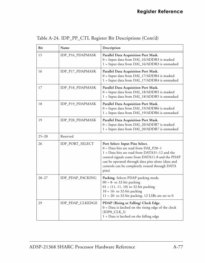
ADSP-21368 SHARC Processor Hardware Reference A-77
Register Reference
15 IDP_P16_PDAPMASK Parallel Data Acquisition Port Mask.0 = Input data from DAI_16/ADDR3 is masked1 = Input data from DAI_16/ADDR3 is unmasked
16 IDP_P17_PDAPMASK Parallel Data Acquisition Port Mask.0 = Input data from DAI_17/ADDR4 is masked1 = Input data from DAI_17/ADDR4 is unmasked
17 IDP_P18_PDAPMASK Parallel Data Acquisition Port Mask.0 = Input data from DAI_18/ADDR5 is masked1 = Input data from DAI_18/ADDR5 is unmasked
18 IDP_P19_PDAPMASK Parallel Data Acquisition Port Mask.0 = Input data from DAI_19/ADDR6 is masked1 = Input data from DAI_19/ADDR6 is unmasked
19 IDP_P20_PDAPMASK Parallel Data Acquisition Port Mask.0 = Input data from DAI_20/ADDR7 is masked1 = Input data from DAI_20/ADDR7 is unmasked
25–20 Reserved
26 IDP_PORT_SELECT Port Select: Input Pins Select.0 = Data bits are read from DAI_P20–1 1 = Data bits are read from DATA31–12 and the control signals come from DATA11-8 and the PDAP can be operated through data pins alone (data and controls can be completely routed through DATA pins)
28–27 IDP_PDAP_PACKING Packing. Selects PDAP packing mode.00 = 8- to 32-bit packing01 = (11, 11, 10) to 32-bit packing10 = 16- to 32-bit packing11 = 20- to 32-bit packing. 12 LSBs are set to 0
29 IDP_PDAP_CLKEDGE PDAP (Rising or Falling) Clock Edge. 0 = Data is latched on the rising edge of the clock (IDP0_CLK_I)1 = Data is latched on the falling edge
Table A-24. IDP_PP_CTL Register Bit Descriptions (Cont’d)
Bit Name Description

Pulse Width Modulation Registers
A-78 ADSP-21368 SHARC Processor Hardware Reference
Pulse Width Modulation RegistersThe following registers control the operation of pulse width modulation on the ADSP-21367/8/9 and ADSP-2137x processors.
PWM Global Control Register (PWMGCTL)Use this register, shown in Figure A-31, to enable or disable the four PWM groups in any combination. This provides synchronization across the groups. This 16-bit, read/write register is located at address 0x3800.
30 IDP_PDAP_RESET PDAP Reset. Setting this bit (=1) causes the PDAP reset circuit to strobe, then this bit is cleared auto-matically.This bit always returns a value of zero when read.
31 IDP_PDAP_EN PDAP Enable. 0 = Disables the 20 DAI pins or the DATA31–8 pins from use as parallel input channels.1 = Enables either the 20 DAI pins or the DATA31–8 pins to be used as a parallel input chan-nel. IDP channel 0 cannot be used as a serial input port with this setting.
Table A-24. IDP_PP_CTL Register Bit Descriptions (Cont’d)
Bit Name Description

ADSP-21368 SHARC Processor Hardware Reference A-79
Register Reference
PWM Global Status Register (PWMGSTAT)This register, described in Table A-25, provides the status of each PWM group and is located at address 0x3801. The bits in this register are W1C-type (write one-to-clear).
Figure A-31. PWMGCTL Register
Table A-25. PWMGSTAT Register Bit Descriptions
Bit Name Description
0 PWM_STAT0 PWM Group 0 Period Completion Status
1 PWM_STAT1 PWM Group 1 Period Completion Status
2 PWM_STAT2 PWM Group 2 Period Completion Status
3 PWM_STAT3 PWM Group 3 Period Completion Status
15 14 13 12 11 10 9 8 7 6 5 4 3 2 1 0
00 0 0 0 0 0 0 0 0 0 0 0 0 0 0
PWM_DIS3
PWM_DIS1
PWM_EN0PWM_SYNCDIS3PWM Group 3 Disable
PWM Group 1 Disable
PWM Group 0 Disable
PWM_EN1
PWM Group 0 EnablePWM_SYNCEN3PWM Group 3 EnablePWM_SYNCDIS2PWM Group 2 DisablePWM_SYNCEN2PWM Group 2 Enable
PWM_SYNCDIS1PWM Group 1 Disable
PWM_SYNCEN1PWM Group 1 Enable
PWM Group 0 DisablePWM_SYNCDIS0
PWM_DIS0
PWM Group 1 Enable
PWM_EN2PWM Group 2 EnablePWM_DIS2
PWM Group 3 Enable
PWM Group 0 EnablePWM_SYNCEN0
PWM_EN3
PWMGCTL (0x3800)
PWM Group 2 Disable
PWM Group 3 Disable

Pulse Width Modulation Registers
A-80 ADSP-21368 SHARC Processor Hardware Reference
PWM Control Register (PWMCTLx)These registers, described in Table A-26, are used to set the operating modes of each PWM block. These registers also allow programs to disable interrupts from individual groups. These registers addresses are:
PWMCTL0 — 0x3000
PWMCTL1 — 0x3010
PWMCTL2 — 0x3400
PWMCTL3 — 0x3410
Table A-26. PWMCTLx Register Bit Descriptions
Bit Name Function
0 PWM_ALIGN Align Mode.0 = Edge-aligned. The PWM waveform is left-justified in the period window.1 = Center-aligned. The PWM waveform is symmetrical.
1 PWM_PAIR Pair Mode.0 = Non-paired mode. The PWM generates independent signals1 = Paired mode. The PWM generates complementary signals on two outputs.
2 PWM_UPDATE Update Mode. 0 = Single-update mode. The duty cycle values are programma-ble only once per PWM period. The resulting PWM patterns are symmetrical about the midpoint of the PWM period.1 = Double-update mode. A second update of the PWM registers is implemented at the midpoint of the PWM period.
5 PWM_IRQEN Enable PWM Interrupts. Enables interrupts.0 = Interrupts not enabled1 = Interrupts enabled

ADSP-21368 SHARC Processor Hardware Reference A-81
Register Reference
PWM Status Registers (PWMSTATx)These 16-bit read-only registers, described in Table A-27, report the sta-tus of the phase and mode for each PWM group. The addresses for these registers are:
PWM Period Registers (PWMPERIODx)These 16-bit read/write registers control the period of the four PWM groups. The value written to the PWMPERIODx register is effectively the number of tCK clock increments in one-half a PWM period. The addresses for these registers are:
PWMSTAT0 — 0x3001
PWMSTAT1 — 0x3011
PWMSTAT2 — 0x3401
PWMSTAT3 — 0x3411
Table A-27. PWMSTATx Register Bit Descriptions
Bit Name Description
0 PWM_PHASE PWM Phase Status. Set during operation in the second half of each PWM period. Allows programs to determine the particular half-cycle during implementation of the PWMSYNC interrupt service routine, if required.0 = First half1 = Second half
2 PWM_PAIRSTAT PWM Paired Mode Status.0 = Inactive paired mode1 = Active paired mode
PWMPERIOD0 — 0x3002
PWMPERIOD1 — 0x3012
PWMPERIOD2 — 0x3402
PWMPERIOD3 — 0x3412

Pulse Width Modulation Registers
A-82 ADSP-21368 SHARC Processor Hardware Reference
PWM Output Disable Registers (PWMSEGx)These 16-bit read/write registers, described in Table A-28, control the output signals of the four PWM groups. The addresses for these registers are:
PWMSEG0 — 0x3008
PWMSEG1 — 0x3018
PWMSEG2 — 0x3408
PWMSEG3 — 0x3418
Table A-28. PWMSEGx Register Bit Descriptions
Bit Name Description
0 PWM_BH Channel B High Disable. Enables or disables the channel B output signal.0 = Enable1 = Disable
1 PWM_BL Channel B Low Disable. Enables or disables the channel B out-put signal.0 = Enable1 = Disable
2 PWM_AH Channel A High Disable. Enables or disables the channel A output signal.0 = Enable1 = Disable
3 PWM_AL Channel A Low Disable. Enables or disables the channel A output signal.0 = Enable1 = Disable

ADSP-21368 SHARC Processor Hardware Reference A-83
Register Reference
PWM Polarity Select Registers (PWMPOLx)These registers, described in Table A-29, control the polarity of the four PWM groups which can be set to either active hi or active lo. The addresses for these registers are:
PWMPOL0 — 0x300F
PWMPOL1 — 0x301F
PWMPOL2 — 0x340F
PWMPOL3 — 0x341F
Table A-29. PWMPOLx Register Bit Descriptions
Bit Name Description
0 PWM_POL1AL Write to Set Channel A Low Polarity 1
1 PWM_POL0AL Write to Set Channel A Low Polarity 0
2 PWM_POL1AH Write to Set Channel A High Polarity 1
3 PWM_POL0AH Write to Set Channel A High Polarity 0
4 PWM_POL1BL Write to Set Channel B Low Polarity 1
5 PWM_POL0BL Write to Set Channel B Low Polarity 0
6 PWM_POL1BH Write to set channel B High Polarity 1
7 PWM_POL0BH Write to set channel B High Polarity 0

Pulse Width Modulation Registers
A-84 ADSP-21368 SHARC Processor Hardware Reference
PWM Channel Duty Control Registers (PWMAx, PWMBx)
The duty cycle control registers, described in Table A-30, directly control the duty cycles of the two pairs of PWM signals. These 16-bit, read/write registers are located at addresses:
PWM Channel Low Duty Control Registers (PWMALx, PWMBLx)
In non-paired mode, these registers, described in Table A-31 are used to program the low side duty cycle. These can be different then the high-side cycles. These 16-bit read/write registers are located at addresses:
PWMA0 — 0x3005 PWMB0 — 0x3006
PWMA1 — 0x3015 PWMB1 — 0x3016
PWMA2 — 0x3405 PWMB2 — 0x3406
PWMA3 — 0x3415 PWMB3 — 0x3416
Table A-30. PWMAx/PWMBx Register Bit Descriptions
Bit Name Description
15–0 PWMAx Channel A Duty Cycle. Program a two’s complement duty cycle with a value of 0x0000 through 0xFFFF. Default = 0
15–0 PWMBx Channel B Duty Cycle. Program a two’s complement duty cycle with a value of 0x0000 through 0xFFFF. Default = 0
PWMAL0 — 0x300A PWMBL0 — 0x300B
PWMAL1 — 0x301A PWMBL1 — 0x301B
PWMAL2 — 0x340A PWMBL2 — 0x340B
PWMAL3 — 0x341A PWMBL3 — 0x341B

ADSP-21368 SHARC Processor Hardware Reference A-85
Register Reference
PWM Dead Time Registers (PWMDTx)These registers, described in Table A-32, set up a short time delay between turning off one PWM signal and turning on its complementary signal. These 10-bit, read/write registers are located at addresses:
Table A-31. PWMALx/PWMBLx Register Bit Descriptions
Bit Name Description
15–0 PWMALx Channel AL Duty Cycle. Program a two’s complement duty cycle with a value of 0x0000 through 0xFFFF. Default = 0
15–0 PWMBLx Channel BL Duty Cycle. Program a two’s complement duty cycle with a value of 0x0000 through 0xFFFF. Default = 0
PWMDT0—0x3003 PWMDT2—0x3403
PWMDT1—0x0013 PWMDT3—0x3413
Table A-32. PWMDTx Register Bit Descriptions
Bit Name Description
9–0 PWMDT PWM Dead Time (unsigned). Program a time delay setting of 0x0000 to 0x03FF. Default = 0
15–10 Reserved

Sony/Philips Digital Interface Registers
A-86 ADSP-21368 SHARC Processor Hardware Reference
Sony/Philips Digital Interface RegistersThe following sections describe the registers that are used to configure, enable and report status information for the S/PDIF transceiver.
Transmitter Control Register (DITCTL)The S/PDIF transmit control register (DITCTL) is a 32-bit, read/write reg-ister located at address 0x24A0. The register’s bits are shown in Figure A-32, Figure A-33 and described in Table A-33.
Figure A-32. DITCTL Register (Bits 31–16)
31 30 29 28 27 26 25 24 23 22 21 20 19 18 17 16
00 0 0 0 0 0 0 0 0 0 0 0 0 0 0
DIT_B0CHANRChannel Status Byte 0 For Subframe B
DITCTL (0x24A0)
DIT_B0CHANLChannel Status Byte 0 for Subframe A

ADSP-21368 SHARC Processor Hardware Reference A-87
Register Reference
Figure A-33. DITCTL Register (Bits 15–0)
Table A-33. DITCTL Register Bit Descriptions
Bit Name Description
0 DIT_EN Transmitter Enable. Enables the transmitter and resets the control registers to their defaults.0 = Transmitter disabled1 = Transmitter enabled
1 DIT_MUTE Mute. Mutes the serial data output.
DIT_EN
DIT_MUTE
DIT_VALIDL
DIT_VALIDR
Validity bit B use with channel status buffer
Validity bit A use with channel status buffer
Mute Serial Data Output 0=Not muted1=Muted
Transmitter Enable0=Transmitter disabled1=Transmitter enabled
15 14 13 12 11 10 9 8 7 6 5 4 3 2 1 0
00 0 0 0 0 0 0 0 0 0 0 0 0 0 0
Reserved
DIT_SMODE_INSerial Data Input Format000=Left-justified001=I2S010–011=Reserved100=Right-justified, 24 bits101=Right-justified, 20 bits110=Right-justified, 18 bits111=Right-justified, 16 bits
DIT_FREQOversampling Ratio 00=256 x Fs01=384 x Fs10=512 x Fs11=786 x FsDIT_SCDFSingle Channel Double Fre-quency Mode Enable0=Disabled, 2 channel mode1=EnabledDIT_SCDF_LRSelect SCDF Channel0=Left channel1=Right channel
DIT_EXT_SYNCEN
External Sync Enable0=Internal frame counter not set to zero at the next LRCLK rising edge1=Internal frame counter is set to zero at the next LRCLK rising edge
DIT_STANDALONE_MODEStandalone Mode0=Full serial mode1=Standalone mode
DIT_USERS
This bit is high if user bits buffer has been written but not fully transmitted.
DIT_BLK_STATBlock Status (Based on Bit 9 = 1)0 =Current word is not block start1 =Current word is block start

Sony/Philips Digital Interface Registers
A-88 ADSP-21368 SHARC Processor Hardware Reference
3–2 DIT_FREQ Frequency Multiplier. Sets the oversampling ratio to the fol-lowing:00 = 256 x Frame sync01 = 384 x Frame sync10 = 512 x Frame sync11 = 768 x Frame sync
4 DIT_SCDF Transmit Single-Channel, Double-Frequency Enable.
5 DIT_SCDF_LR Select single-channel, double-frequency mode channel. (L = 0, R = 1)
8–6 DIT_SMODEIN Serial Data Input Format. Select the input format as follows:000 = Left-justified001 = I2S010 = Reserved 011 = Reserved 100 = Right-justified, 24-bits101 = Right-justified, 20-bits110 = Right-justified, 18-bits111 = Right-justified, 16-bits
9 DIT_STANDALONE_MODE
Standalone Mode Enable. When this bit is set (=1), the trans-mitter is in standalone mode. In this mode the transmitter inserts block start bits automatically. Channel status bits and user bits are taken from the respective buffers. Valid bit is set based on bits 10 and 11 in this DITCTL register for channel A and B respectively. Bits received with serial data are ignored. When this bit is cleared (=0), the transmitter is in full serial mode. In this mode, all the status bits, including the block start bit, (indicating start of a frame) come through the SDATA pin along with audio data. The transmitter should be enabled after or with all other control bits.
10 DIT_VALIDL Validity Bit A. Use with channel status buffer.
11 DIT_VALIDR Validity Bit B. Use with channel status buffer.
12 DIT_BLK_STAT Block Status (read-only). Status bit that indicates block start (when bit 9, DIT_AUTO, = 1).0 = Current word is not block start1 = Current word is block start
Table A-33. DITCTL Register Bit Descriptions (Cont’d)
Bit Name Description

ADSP-21368 SHARC Processor Hardware Reference A-89
Register Reference
Left Channel Status for Subframe A Registers (DITCHANAx)
There are six channel status buffer registers associated with subframe A. These registers are listed with their locations in Table A-34.
13 DIT_USERS User Bits Status. This bit is high if user bits buffer has been written but data has not been transmitted completely.
14 Reserved
15 DIT_EXT_SYNCEN External Sync Enable. When this bit is set, the internal frame counter is set to zero at the next LRCLK rising edge.
23–16 DIT_B0CHANL Channel status byte 0 for subframe A
31–24 DIT_B0CHANR Channel status byte 0 for subframe B
Table A-34. DITCHANAx Registers
Register (Address) Bits 7–0 Bits 15–8 Bits 23–16 Bits 31–24
DITCHANA0 (0x24A1) BYTE1 BYTE2 BYTE3 BYTE4
DITCHANA1 (0x24D4) BYTE5 BYTE6 BYTE7 BYTE8
DITCHANA2 (0x24D5) BYTE9 BYTE10 BYTE11 BYTE12
DITCHANA3 (0x24D6) BYTE13 BYTE14 BYTE15 BYTE16
DITCHANA4 (0x24D7) BYTE17 BYTE18 BYTE19 BYTE20
DITCHANA5 (0x24D8) BYTE21 BYTE22 BYTE23 Reserved
Table A-33. DITCTL Register Bit Descriptions (Cont’d)
Bit Name Description

Sony/Philips Digital Interface Registers
A-90 ADSP-21368 SHARC Processor Hardware Reference
Right Channel Status for Subframe B Registers (DITCHANBx)
There are six channel status buffer registers associated with subframe B. These registers are listed with their locations in Table A-35.
User Bits Buffer Registers for Subframe ARegisters (DITUSRBITAx)
There are six user bits buffer registers associated with subframe A (left channel). These registers are listed with their locations in Table A-36.
Table A-35. DITCHANBx Registers
Register (Address) Bits 7–0 Bits 15–8 Bits 23–16 Bits 31–24
DITCHANB0 (0x24A2) BYTE1 BYTE2 BYTE3 BYTE4
DITCHANB1 (0x24DA) BYTE5 BYTE6 BYTE7 BYTE8
DITCHANB2 (0x24DB) BYTE9 BYTE10 BYTE11 BYTE12
DITCHANB3 (0x24DC) BYTE13 BYTE14 BYTE15 BYTE16
DITCHANB4 (0x24DD) BYTE17 BYTE18 BYTE19 BYTE20
DITCHANB5 (0x24DE) BYTE21 BYTE22 BYTE23 Reserved
Table A-36. DITUSRBITAx Registers
Register (Address) Bits 7–0 Bits 15–8 Bits 23–16 Bits 31–24
DITUSRBITA0 (0x24E0) BYTE0 BYTE1 BYTE2 BYTE3
DITUSRBITA1 (0x24E1) BYTE4 BYTE5 BYTE6 BYTE7
DITUSRBITA2 (0x24E2) BYTE8 BYTE9 BYTE10 BYTE11
DITUSRBITA3 (0x24E3) BYTE12 BYTE13 BYTE14 BYTE15
DITUSRBITA4 (0x24E4) BYTE16 BYTE17 BYTE18 BYTE19
DITUSRBITA5 (0x24E5) BYTE20 BYTE21 BYTE22 BYTE23

ADSP-21368 SHARC Processor Hardware Reference A-91
Register Reference
User Bits Buffer Registers for Subframe B Registers (DITUSRBITBx)
There are six user bits buffer registers associated with subframe B (right channel). These registers are listed with their locations in Table A-37.
Table A-37. DITUSRBITBx Registers
Register (Address) Bits 7–0 Bits 15–8 Bits 23–16 Bits 31–24
DITUSRBITB0 (0x24E8) BYTE0 BYTE1 BYTE2 BYTE3
DITUSRBITB1 (0x24E9) BYTE4 BYTE5 BYTE6 BYTE7
DITUSRBITB2 (0x24EA) BYTE8 BYTE9 BYTE10 BYTE11
DITUSRBITB3 (0x24EB) BYTE12 BYTE13 BYTE14 BYTE15
DITUSRBITB4 (0x24EC) BYTE16 BYTE17 BYTE18 BYTE19
DITUSRBITB5 (0x24ED) BYTE20 BYTE21 BYTE22 BYTE23

Sony/Philips Digital Interface Registers
A-92 ADSP-21368 SHARC Processor Hardware Reference
Receiver Control Register (DIRCTL)This 32-bit read/write register is used to set up error control and sin-gle-channel, double-frequency mode. The register is located at address 0x24A8. The register’s bits are shown in Figure A-34 and described in Table A-38.
Figure A-34. DIRCTL Register
31 30 29 28 27 26 25 24 23 22 21 20 19 18 17 16
00 0 0 0 0 0 0 0 0 0 0 0 0 0 0
DIR_BIPHASE
DIR_PLLDISDisable PLL 0=Use derived clock from the digital PLL1=Use clock input from external PLL
Parity Biphase Error Control 00=No action taken01=Hold last valid sample10=Replace invalid sample with zeros11=Reserved
DIRCTL (0x24A8)
15 14 13 12 11 10 9 8 7 6 5 4 3 2 1 0
00 0 0 0 0 0 0 0 0 0 0 0 0 0 0
Reserved
Reserved
DIR_LOCKLock Error Control00=No action taken01=Hold last valid sample10=Send zeros after the last valid sample11=Soft mute of the last valid audio sample is performed
DIR_MUTEMute0=Mute disabled1=Mute serial data outputs, maintaining clocks (digital black)
DIR_SCDFSingle-Channel, Double-Frequency Mode Enable0=2 channel mode disabled1=2 channel mode enabled
DIR_SCDF_LRSingle-Channel, Double-Frequency Channel Select0=Left channel1=Right channel

ADSP-21368 SHARC Processor Hardware Reference A-93
Register Reference
Table A-38. DIRCTL Register Bit Descriptions
Bit Name Description
1–0 DIR_BIPHASE Parity Biphase Error Control. 00 = No action taken01 = Hold last valid sample10 = Replace invalid sample with zeros11 = Reserved
3–2 DIR_LOCK Lock Error Control. 00 = No action taken01 = Hold last valid sample10 = Send zeros after the last valid sample11 = Soft mute of the last valid audio sample is performed as if NOSTREAM is asserted. This is valid only when linear PCM audio data is in the stream. With non-linear audio data, this mode defaults to LOCKERROR_CTL = 10.
4 DIR_SCDF_LR Single-Channel, Double-Frequency Channel Select. 0 = Left channel1 = Right channel
5 DIR_SCDF Single-Channel, Double-Frequency Mode Enable. 0 = 2 channel mode disabled1 = 2 channel mode enabled
6 DIR_MUTE Mute.0 = Mute disabled1 = Mute serial data outputs, maintaining clocks (digital black)
7 DIR_PLLDIS Disable PLL. Determines clock input.0 = Use derived clock from the digital PLL1 = Use clock input from external PLL
31–8 Reserved

Sony/Philips Digital Interface Registers
A-94 ADSP-21368 SHARC Processor Hardware Reference
Receiver Status Register (DIRSTAT)This 32-bit, read-only register is used to store the error bits. The error bits are sticky on read. Once they are set, they remain set until the register is read. This register also contains the lower byte of the 40-bit channel status information. The register is located at address 0x24A9. The register’s bits are shown in Figure A-35 and described in Table A-39.
Figure A-35. DIRSTAT Register
31 30 29 28 27 26 25 24 23 22 21 20 19 18 17 16
00 0 0 0 0 0 0 0 0 0 0 0 0 0 0
DIR_NOAUDIOL
DIR_BIPHASEERROR
Biphase Error0=No biphase error1=Biphase error
Non-Audio Subframe Mode Channel 10=Not non-audio subframe mode1=Non-audio subframe mode, channel 1
DIRSTAT (0x24A9)
15 14 13 12 11 10 9 8 7 6 5 4 3 2 1 0
00 0 0 0 0 0 0 0 0 0 0 0 0 0 0
DIR_B0CHANL
Reserved
DIR_VALIDValidity Bit. ORed Value of Channel 1 and 20=Linear PCM data1=Non-linear audio data
DIR_PARITYERRORParity Bit. Indicates Parity Error0=No parity error1=Parity error
DIR_NOSTREAMStream Disconnected0=Stream not disconnected1=Stream disconnected
DIR_LOCKLock Receiver0=Receiver not locked1=Receiver locked
DIR_NOAUDIORNon-Audio Subframe Mode Channel 20=Not non-audio subframe mode1=Non-audio subframe mode, channel 2DIR_NOAUDIOLRNon-Audio Subframe Mode Channel 1 and 20=Not non-audio frame mode1=Non audio frame mode
DIR_B0CHANR
Channel Status Byte 0 for Subframe A
Channel Status Byte 0 for Subframe B

ADSP-21368 SHARC Processor Hardware Reference A-95
Register Reference
Table A-39. DIRSTAT Register Bit Descriptions
Bit Name Description
0 DIR_NOAUDIOL Non-Audio Subframe Mode Channel 1. Based on SMPTE 337M.0 = Not non-audio subframe mode1 = Non-audio subframe mode, Channel 1
1 DIR_NOAUDIOR Non-Audio Subframe Mode Channel 2. Based on SMPTE 337M.0 = Not non-audio subframe mode1 = Non-audio subframe mode, Channel 2
2 DIR_NOAUDIOLR Non-Audio Frame Mode Channel 1 and 2. Based on SMPTE 337M.0 = Not non-audio frame mode1 = Non audio frame mode
3 DIR_VALID Validity Bit. ORed value of channel 1 and 2.0 = Linear PCM data1 = Non-linear audio data
4 DIR_LOCK Lock Receiver. 0 = Receiver not locked1 = Receiver locked
5 DIR_NOSTREAM Stream Disconnected. Indicates that the data stream is disconnected.0 = Stream not disconnected1 = Stream disconnected
6 DIR_PARITYERROR Parity Bit. Indicates parity error.0 = No parity error1 = Parity error
7 DIR_BIPHASEERROR Biphase Error Indicates biphase error.0 = No biphase error1 = Biphase error
15–8 Reserved
23–16 DIR_B0CHANL Channel Status Byte 0 for Subframe A.
31–24 DIR_B0CHANR Channel Status Byte 0 for Subframe B.

Sony/Philips Digital Interface Registers
A-96 ADSP-21368 SHARC Processor Hardware Reference
Left Channel Status for Subframe A Register (DIRCHANL)
This register (DIRCHANL, described in Table A-40) is a 32-bit, read/write register located at address 0x24AA.
Right Channel Status for Subframe B Register (DIRCHANR)
This register (DIRCHANR, described in Table A-41) is a 32-bit, read/write register located at address 0x24AB.
Table A-40. DIRCHANL Register
Bit Name Description
7–0 DIR_B1CHANL Channel status byte 1 for subframe A
15–8 DIR_B2CHANL Channel status byte 2 for subframe A
23–16 DIR_B3CHANL Channel status byte 3 for subframe A
31–24 DIR_B4CHANL Channel status byte 4 for subframe A
Table A-41. DIRCHANR Register
Bit Name Description
7–0 DIR_B1CHANR Channel status byte 1 for subframe B
15–8 DIR_B2CHANR Channel status byte 2 for subframe B
23–16 DIR_B3CHANR Channel status byte 3 for subframe B
31–24 DIR_B4CHANR Channel status byte 4 for subframe B

ADSP-21368 SHARC Processor Hardware Reference A-97
Register Reference
Sample Rate Converter RegistersThe sample rate converter (SRC) is composed of five registers which are described in the following sections.
SRC Control Registers (SRCCTLx)These registers (read/write) control the operating modes, filters, and data formats used in the SRCs and are shown in Figure A-36 through Figure A-39 and described in Table A-42 and Table A-43. The SRCCTL0 register controls the SRC0 and SRC1 modules and SRCCTL1 register con-trols the SRC2 and SRC3 modules.
Figure A-36. SRCCTL0 Register (Bits 16–31)
31 30 29 28 27 26 25 24 23 22 21 20 19 18 17 16
00 0 0 0 0 0 0 0 0 0 0 0 0 0 0SRCCTL0 (0x2490)
SRC1_ENABLESRC1 Enable1=SRC enabled0=SRC disabled
SRC1_MPHASESRC1 Matched- Phase Mode 1=Enabled0=Disabled
SRC1_LENOUTSRC1 Output Word Length 00=24-bit, 01=20-bit10=18-bit, 11=16-bit
SRC1_SMODEOUTSRC1 Serial Output Format00=Left-justified (default)01=I2S10=TDM Mode11=Right-justified
SRC1_DITHERSRC1 Dither Enable 1=Enable0=Disable
SRC1 Soft Mute Enable1=Mute (default)0=No mute
SRC1_SOFTMUTE
SRC1_HARD_MUTESRC1 Hard Mute Enable1=Enabled0=Disabled
SRC1_AUTO_MUTESRC1 Auto Hard Mute Enable (from SPDIF RX)1=Enabled0=Disabled
SRC1_BYPASS
SRC1 De-emphasis Filter1=Enabled0=Disabled (default)
SRC1 Bypass Mode1=Bypass enabled0=Bypass disabled
SRC1_DEEMPHASIS
SRC1_SMODEINSRC1 Serial Input Format000=Left-justified (Default)001=I2S010=TDM100=24-bit right-justified101=20-bit right-justified110=18-bit right-justified111=16-bit right-justified

Sample Rate Converter Registers
A-98 ADSP-21368 SHARC Processor Hardware Reference
Figure A-37. SRCCTL0 Register (Bits 0–15)
Table A-42. SRCCTL0 Register Bit Descriptions
Bit Name Description
0 SRC0_HARD_MUTE Hard Mute. Hard mutes SRC 0.1 = Mute (default)
1 SRC0_AUTO_MUTE Auto Hard Mute. Auto hard mutes SRC 0 when one of the non-audio bits is asserted by the SPDIF receiver. See Table A-39 on page A-95.0 = No mute1 = Mute (default)
15 14 13 12 11 10 9 8 7 6 5 4 3 2 1 0
00 0 0 0 0 0 0 0 0 0 0 0 0 0 0
SRC0_HARD_MUTESRC0_RESETSRC0 Reset1=SRC enabled0=SRC disabled
SRC0 Hard Mute Enable1=Enabled0=Disabled
SRC0_AUTO_MUTESRC0 Auto Hard Mute Enable (from SPDIF RX)1=Enabled0=Disabled
SRC0_BYPASS
SRC0 De-emphasis Filter1=Enabled0=Disabled (default)
SRC0 Bypass Mode1=Bypass enabled0=Bypass disabled
SRC0_DEEMPHASIS
SRC0_MPHASESRC0 Matched-Phase Mode 1=Enabled0=Disabled
SRC0_LENOUTSRC0 Output Word Length 00=24-bit, 01=20-bit10=18-bit, 11=16-bit
SRC0_SMODEOUTSRC0 Serial Output Format00=Left-justified (default)01=I2S10=TDM 11=Right-justified
SRC0_DITHERSRC Dither Enable 1=Enable0=Disable
SRC0 Soft Mute Enable1=Mute (default)0=No Mute
SRC0_SOFTMUTE
SRC0_SMODEINSRC0 Serial Input Format000=Left-justified (Default)001=I2S010=TDM100=24-bit right-justified101=20-bit right-justified110=18-bit right-justified111=16-bit right-justified
SRCCTL0 (0x2490)

ADSP-21368 SHARC Processor Hardware Reference A-99
Register Reference
4–2 SRC0_SMODEIN Serial Input Format. Selects the serial input format for SRC 0 as follows.000 = Default, format is left-justified001 = I2S010 = TDM100 = 24-bit right-justified101 = 20-bit right-justified110 = 18-bit right-justified111 = 16-bit right-justified
5 SRC0_BYPASS Bypass SRC0. Output of SRC 0 is the same as the input.
7–6 SRC0_DEEMPHASIS De-emphasis Filter Select. Enables de-emphasis on incoming audio data for SRC 0.00 = No Deemphasis01 = 33 kHz10 = 44.1 kHz11 = 48 kHz
8 SRC0_SOFTMUTE Soft Mute. Enables soft mute on SRC 0.0 = No mute1 = Mute (default)
9 SRC0_DITHER Dither Select. Enables dithering on SRC 0 when a word length less than 24 bits is selected.0 = Dithering is disabled (default)1 = Dithering is enabled
11–10 SRC0_SMODEOUT Serial Output Format. Selects the serial output format on SRC 0, as follows:00 = Left-justified (default)01 = I2S10 = TDM mode11 = Right-justified
Table A-42. SRCCTL0 Register Bit Descriptions (Cont’d)
Bit Name Description

Sample Rate Converter Registers
A-100 ADSP-21368 SHARC Processor Hardware Reference
13–12 SRC0_LENOUT Output Word Length Select. Selects the serial output word length on SRC 0 as follows:00 = 24 bits01 = 20 bits10 = 18 bits11 = 16 bitsAny word length less than 24 bits will have dither added to the unused LSBs if SRCx_DITHER is enabled (= 1).
14 SRC0_MPHASE Match-Phase Mode Select. Configures the SRC 0 mod-ules to not use their own internally-generated sample rate ratio but use an externally-generated ratio. Used with TDM data. 0 = Matched-phase mode disabled (default)1 = Matched-phase mode enabled
15 SRC0_ENABLE SRC0 Enable. Enables SRC 0.0 = Disabled1 = Enabled
16 SRC1_HARD_MUTE Hard Mute. Hard mutes SRC 1.1 = Mute (default)
17 SRC1_AUTO_MUTE Auto Hard Mute. Auto hard mutes SRC 1 when one of the non-audio bits is asserted by the SPDIF receiver. See Table A-39 on page A-95.0 = No mute1 = Mute (default)
20–18 SRC1_SMODEIN Serial Input Format. Selects the serial input format for SRC 1 as follows.000 = Default, format is left-justified001 = I2S010 = TDM100 = 24-bit right-justified101 = 20-bit right-justified110 = 18-bit right-justified111 = 16-bit right-justified
21 SRC1_BYPASS Bypass Mode Enable. Output of SRC 1 is the same as input.
Table A-42. SRCCTL0 Register Bit Descriptions (Cont’d)
Bit Name Description

ADSP-21368 SHARC Processor Hardware Reference A-101
Register Reference
23–22 SRC1_DEEMPHASIS De-emphasis Filter Select. Enables deemphasis on incoming audio data for SRC 1.00 = No de-emphasis01 = 33 kHz10 = 44.1 kHz11 = 48 kHz
24 SRC1_SOFTMUTE Soft Mute. Enables soft mute on SRC 1.0 = No mute1 = Mute (default)
25 SRC1_DITHER Dither Select. Disables dithering on SRC 1 when a word length less than 24 bits is selected.0 = Dithering is disabled (default)1 = Dithering is enabled
27–26 SRC1_SMODEOUT Serial Output Format. Selects the serial output format for SRC 1 as follows.00 = Left-justified (default)01 = I2S10 = TDM mode11 = Right-justified
29–28 SRC1_LENOUT Output Word Length Select. Selects the serial output word length for SRC 1 as follows.00 = 24 bits01 = 20 bits10 = 18 bits11 = 16 bitsAny word length less than 24 bits will have dither added to the unused LSBs if SRCx_DITHER is enabled (= 1).
30 SRC1_MPHASE Match-Phase Mode Select. Configures the SRC 1 mod-ules to not use their own internally-generated sample rate ratio but use an externally-generated ratio. Used with TDM data. 0 = Matched-phase disabled (default)1 = Matched-phase enabled
31 SRC1_ENABLE SRC Enable. Enables SRC 1.0 = Disabled1 = Enabled
Table A-42. SRCCTL0 Register Bit Descriptions (Cont’d)
Bit Name Description

Sample Rate Converter Registers
A-102 ADSP-21368 SHARC Processor Hardware Reference
Figure A-38. SRCCTL1 Register (Bits 16–31)
31 30 29 28 27 26 25 24 23 22 21 20 19 18 17 16
00 0 0 0 0 0 0 0 0 0 0 0 0 0 0SRCCTL1 (0x2491)
SRC3_ENABLESRC 3 Enable1=SRC enabled0=SRC disabledSRC3_MPHASESRC 3 Matched-Phase Mode 1=Enabled0=DisabledSRC3_LENOUTSRC 3 Output Word Length 00=24-bit01=20-bit10=18-bit11=16-bit
SRC3_SMODEOUTSRC 3 Serial Output Format00=Left-justified (default)01=I2S10=TDM11=Right-justified
SRC3_DITHERSRC 3 Dither Enable 1=Enable0=Disable
SRC 3 Soft Mute Enable1=Mute (default)0=No mute
SRC3_SOFTMUTE
SRC3_HARD_MUTESRC 3 Hard Mute Enable1=Enabled0=DisabledSRC3_AUTO_MUTESRC 3 Auto Hard Mute Enable (from SPDIF RX)1=Enabled0=Disabled
SRC3_BYPASS
SRC 3 De-emphasis Filter1=Enabled0=Disabled (default)
SRC 3 Bypass Mode1=Bypass enabled0=Bypass disabled
SRC3_DEEMPHASIS
SRC3_SMODEIN
SRC 3 Serial Input Format000=Left-justified (Default)001=I2S010=TDM100=24-bit right-justified101=20-bit right-justified110=18-bit right-justified111=16-bit right-justified

ADSP-21368 SHARC Processor Hardware Reference A-103
Register Reference
Figure A-39. SRCCTL1 Register (Bits 0–15)
Table A-43. SRCCTL1 Register Bit Descriptions
Bit Name Description
0 SRC2_HARD_MUTE Hard Mute. Hard mutes SRC 2.1 = Mute (default)
1 SRC2_AUTO_MUTE Auto Hard Mute. Auto hard mutes SRC 2 when one of the non-audio bits is asserted by the SPDIF receiver. See Table A-39 on page A-95.0 = No mute1 = Mute (default)
15 14 13 12 11 10 9 8 7 6 5 4 3 2 1 0
00 0 0 0 0 0 0 0 0 0 0 0 0 0 0
SRC2_HARD_MUTESRC2_RESETSRC0, 2 Reset1=SRC enabled0=SRC disabled
SRC 2 Hard Mute Enable1=Enabled0=Disabled
SRC2_AUTO_MUTESRC 2 Auto Hard Mute Enable (from SPDIF RX)1=Enabled0=Disabled
SRC2_BYPASS
SRC 2 Deemphasis Filter1=Enabled0=Disabled (default)
SRC 2 Bypass Mode1=Bypass enabled0=Bypass disabled
SRC2_DEEMPHASIS
SRC2_MPHASESRC 2 Matched-Phase Mode 1=Enabled0=Disabled
SRC2_LENOUTSRC 2 Output Word Length 00=24-bit, 01=20-bit10=18-bit, 11=16-bit
SRC2_SMODEOUTSRC 2 Serial Output Format00=Left-justified (default)01=I2S10=TDM 11=Right-justified
SRC2_DITHERSRC 2 Dither Enable 1=Enable0=Disable
SRC 2 Soft Mute Enable1=Mute (default)0=No mute
SRC2_SOFTMUTE
SRC2_SMODEINSRC 2 Serial Input Format000=Left-justified (default)001=I2S010=TDM100=24-bit right-justified101=20-bit right-justified110=18-bit right-justified111=16-bit right-justified
SRCCTL1 (0x2491)

Sample Rate Converter Registers
A-104 ADSP-21368 SHARC Processor Hardware Reference
4–2 SRC2_SMODEIN Serial Input Format. Selects the serial input format for SRC 2 as follows.000 =Default, format is left-justified001 = I2S010 = TDM100 = 24-bit right-justified101 = 20-bit right-justified110 = 18-bit right-justified111 = 16-bit right-justified
5 SRC2_BYPASS Bypass SRCx. Output of SRC 2 is the same as input
7–6 SRC2_DEEMPHASIS De-emphasis Filter Select. Enables de-emphasis on incoming audio data for SRC 2.00 = No de-emphasis01 = 33 kHz10 = 44.1 kHz11 = 48 kHz
8 SRC2_SOFTMUTE Soft Mute. Enables soft mute on SRC 2.0 = No mute1 = Mute (default)
9 SRC2_DITHER Dither Select. Enables dithering on SRC 2 when a word length less than 24 bits is selected.0 = Dithering is disabled (default)1 = Dithering is enabled
11–10 SRC2_SMODEOUT Serial Output Format. Selects the serial output format on SRC 2 as follows:00 = Left-justified (default)01 = I2S10 = TDM mode11 = Right-justified
Table A-43. SRCCTL1 Register Bit Descriptions (Cont’d)
Bit Name Description

ADSP-21368 SHARC Processor Hardware Reference A-105
Register Reference
13–12 SRC2_LENOUT Output Word Length Select. Selects the serial output word length on SRC 2 as follows:00 = 24 bits01 = 20 bits10 = 18 bits11 = 16 bitsAny word length less than 24 bits will have dither added to the unused LSBs if SRCx_DITHER is enabled (= 1).
14 SRC2_MPHASE Match-Phase Mode Select. Configures the SRC 2 mod-ules to not use their own internally-generated sample rate ratio but use an externally-generated ratio. Used with TDM data. 0 = Matched-phase disabled (default)1 = Matched-phase enabled
15 SRC2_ENABLE SRCx Enable. Enables SRC 2.0 = Disabled1 = Enabled
16 SRC3_HARD_MUTE Hard Mute. Hard mutes SRC 3.1 = Mute (default)
17 SRC3_AUTO_MUTE Auto Hard Mute. Auto hard mutes SRC 3 when one of the non-audio bits is asserted by the SPDIF receiver. See Table A-39 on page A-95.0 = No mute1 = Mute (default)
20–18 SRC3_SMODEIN Serial Input Format. Selects the serial input format for SRC 3 as follows:000 = Default, format is left-justified001 = I2S010 = TDM100 = 24-bit right-justified101 = 20-bit right-justified110 = 18-bit right-justified111 = 16-bit right-justified
21 SRC3_BYPASS Bypass Mode Enable. Output of SRC 3 is the same as input.
Table A-43. SRCCTL1 Register Bit Descriptions (Cont’d)
Bit Name Description

Sample Rate Converter Registers
A-106 ADSP-21368 SHARC Processor Hardware Reference
23–22 SRC3_DEEMPHASIS De-emphasis Filter Select. Enables de-emphasis on incoming audio data for SRC 3.00 = No de-emphasis01 = 33 kHz10 = 44.1 kHz11 = 48 kHz
24 SRC3_SOFTMUTE Soft Mute. Enables soft mute on SRC 3.0 = No mute1 = Mute (default)
25 SRC3_DITHER Dither Select. Disables dithering on SRC 3 when a word length less than 24 bits is selected.0 = Dithering is disabled (default)1 = Dithering is enabled
27–26 SRC3_SMODEOUT Serial Output Format. Selects the serial output format for SRC 3 as follows:00 = Left-justified (default)01 = I2S10 = TDM mode11 = Right-justified
29–28 SRC3_LENOUT Output Word Length Select. Selects the serial output word length for SRC 3 as follows:00 = 24 bits01 = 20 bits10 = 18 bits11 = 16 bitsAny word length less than 24 bits will have dither added to the unused LSBs if SRCx_DITHER is enabled (= 1).
30 SRC3_MPHASE Match-Phase Mode Select. Configures the SRC 3 mod-ules to not use their own internally-generated sample rate ratio but use an externally-generated ratio. Used with TDM data. 0 = Matched-phase disabled (default)1 = Matched-phase enabled
31 SRC3_ENABLE SRC Enable. Enables SRC 3.0 = Disabled1 = Enabled
Table A-43. SRCCTL1 Register Bit Descriptions (Cont’d)
Bit Name Description

ADSP-21368 SHARC Processor Hardware Reference A-107
Register Reference
SRC Mute Register (SRCMUTE)This read-write register, described in Table A-44, connects an SRCx mute input and output (when cleared) to automatically mute input while the SRC is initializing. Bit 0 controls SRC0, bit 1 controls SRC1, bit 2 controls SRC2, and bit 3 controls SRC3. This register is located at address 0x2492. Note that the SRC mute interrupts are latched in the DAI_IRPTL_H and DAI_IRPTL_L registers.
Table A-44. SRCMUTE Register Bit Descriptions
Bit Name Description
0 SRC0_MUTE_EN 0 = Connect SRC0 mute input and output1 = Do not connect SRC0 mute input and output
1 SRC1_MUTE_EN 0 = Connect SRC1 mute input and output1 = Do not connect SRC1 mute input and output
2 SRC2_MUTE_EN 0 = Connect SRC2 mute input and output1 = Do not connect SRC2 mute input and output
3 SRC3_MUTE_EN 0 = Connect SRC3 mute input and output1 = Do not connect SRC3 mute input and output

Sample Rate Converter Registers
A-108 ADSP-21368 SHARC Processor Hardware Reference
SRC Ratio Registers (SRCRATx)These read-only status registers (shown in Figure A-40) report the mute and I/O sample ratio as follows: the SRCRAT0 register reports for SRC0 and 1 and the SRCRAT1 register reports the mute and I/O sample ratio for SRC2 and 3.
Figure A-40. SRC Ratio Register (SRCRAT0)
31 30 29 28 27 26 25 24 23 22 21 20 19 18 17 16
00 0 0 0 0 0 0 0 0 0 0 0 0 0 0
SRC1_RATIOxSRC1_MUTEOUT
15 14 13 12 11 10 9 8 7 6 5 4 3 2 1 0
00 0 0 0 0 0 0 0 0 0 0 0 0 0 0
SRC0_RATIOxSRC0_MUTEOUTSRC0 Mute Output Enabled
SRC1 Ratio Bit Field
SRC0 Ratio Bit Field
SRCRAT0 (0x2498)
SRC1 Mute Output Enabled
31 30 29 28 27 26 25 24 23 22 21 20 19 18 17 16
00 0 0 0 0 0 0 0 0 0 0 0 0 0 0
SRC3_RATIOxSRC3_MUTEOUT
15 14 13 12 11 10 9 8 7 6 5 4 3 2 1 0
00 0 0 0 0 0 0 0 0 0 0 0 0 0 0
SRC2_RATIOxSRC2_MUTEOUT
SRC2 Mute Output Enabled
SRC3 Ratio Bit Field
SRC 2 Ratio Bit Field
SRC_RAT1 (0x2499)
SRC3 Mute Output Enabled

ADSP-21368 SHARC Processor Hardware Reference A-109
Register Reference
DAI/DPI RegistersThe registers that are described in the following sections are contained within the digital audio and digital peripheral interfaces. The bits in these registers are used to enable the connection of peripherals and to view sta-tus of data transfers. For complete information on using the DAI/DPI, see Chapter 4, Digital Audio/Digital Peripheral Interfaces.
Digital Audio Interface Status Register (DAI_STAT)The DAI_STAT register is a read-only register and is shown in Figure A-41 and described in Table A-45. The state of all eight DMA channels is reflected in IDP_DMAx_STAT (bits 24-17 of the DAI_STAT register). These bits are set once the IDP_DMA_EN bit is set and remains set till the last data of that channel is transferred (see “Input Data Port Control Register 0 (IDP_CTL0)” on page A-66). Even if the IDP_DMA_EN bit is set, it goes low once the required number of data transfers occurs. And even when DMA through some channel is not intended, its IDP_DMAx_STAT bit goes high.

DAI/DPI Registers
A-110 ADSP-21368 SHARC Processor Hardware Reference
Figure A-41. DAI_STAT Register
Table A-45. DAI_STAT Register Bit Descriptions
Bit Name Description
7–0 SRU_PINGx_STAT Ping-pong DMA Status (Channel). Indicates the status of ping-pong DMA in each respective channel (channel 0–7).0 = DMA is not active1 = DMA is active
15–8 SRU_OVFx Sticky Overflow Status (Channel). Provides overflow status information for each channel (bit 8 for channel 0 through bit 15 for channel 7).0 = No overflow1 = Overflow has occurred
16 Reserved
31 30 29 28 27 26 25 24 23 22 21 20 19 18 17 16
00 0 0 0 0 0 0 0 0 0 0 0 0 0 0
15 14 13 12 11 10 9 8 7 6 5 4 3 2 1 0
00 0 0 0 0 0 0 0 0 0 0 0 0 0 0
IDP_FIFOSZ
Reserved
Number of Valid Data in IDP FIFO
IDP_DMA7_STAT
IDP_DMA6_STAT
IDP_DMA3_STAT
IDP_DMA4_STAT
IDP_DMA1_STAT
IDP_DMA2_STAT
IDP_DMA0_STAT
IDP_DMA5_STAT
SRU_PING1_STAT
SRU_OVF0
DAI_STAT (0x24B8)
SRU_PING0_STAT
SRU_PING2_STATSRU_PING3_STATSRU_PING4_STATSRU_PING5_STATSRU_PING6_STATSRU_PING7_STAT
SRU_OVF1SRU_OVF2
SRU_OVF4
SRU_OVF7SRU_OVF6SRU_OVF5
SRU_OVF3
Reserved
IDP Channel Overflow (Sticky) Ping-Pong DMA Chan-nel Status
DMA Active Status for IDP Channel

ADSP-21368 SHARC Processor Hardware Reference A-111
Register Reference
DAI Resistor Pull-up Enable Register (DAI_PIN_PULLUP)
This 20-bit, read/write register is shown in Figure A-42. Bits 19–0 of this register control the enabling/disabling 22.5 KΩ pull-up resistor on DAI_P0[19:0]. Setting a bit to 1 enables a pull-up resistor on the corre-sponding pin. After RESET, the value of this register is 0xFFFFF, which means pull-ups are enabled on all 20 DAI pins.
24–17 IDP_DMAx_STAT Input Data Port DMA Status.0 = DMA is not active1 = DMA is active
27–25 Reserved
31–28 IDP_FIFOSZ IDP FIFO Size.Number of samples in the IDP FIFO.
Figure A-42. DAI_PIN_PULLUP Register
Table A-45. DAI_STAT Register Bit Descriptions (Cont’d)
Bit Name Description
31 30 29 28 27 26 25 24 23 22 21 20 19 18 17 16
10 0 0 0 0 0 0 0 0 0 0 0 1 1 1
15 14 13 12 11 10 9 8 7 6 5 4 3 2 1 0
11 1 1 1 1 1 1 1 1 1 1 1 1 1 1
Reserved
DAI_P16_PULLUP
DAI_P20_PULLUP DAI_P19_PULLUP
DAI_P18_PULLUP
DAI_P17_PULLUP
DAI_P15_PULLUP
DAI_P14_PULLUP
DAI_P13_PULLUP
DAI_P12_PULLUP
DAI_P01_PULLUP
DAI_P02_PULLUP
DAI_P03_PULLUP
DAI_P04_PULLUP
DAI_P05_PULLUP
DAI_P06_PULLUPDAI_P11_PULLUP
DAI_P10_PULLUP
DAI_P09_PULLUP
DAI_P07_PULLUP
DAI_P08_PULLUP
DAI_STAT (0x247D)

DAI/DPI Registers
A-112 ADSP-21368 SHARC Processor Hardware Reference
DAI Pin Buffer Status Register (DAI_PIN_STAT)This 20-bit, read-only register is shown in Figure A-43. Bits 19–0 of this register indicate the status of DAI_PB[20:1]. Reads from bits 31–20 always return 0. This register is updated at one-half the core clock rate.
DAI Interrupt Controller RegistersThe DAI contains its own interrupt controller that indicates to the core when DAI audio peripheral related events have occurred. Since audio events generally occur infrequently relative to the SHARC core, the DAI interrupt controller reduces all of its interrupts onto two interrupt signals within the core’s primary interrupt systems—one mapped with low prior-ity and one mapped with high priority. This architecture allows programs to indicate priority broadly. In this way, the DAI interrupt controller reg-isters provide 32 independently configurable interrupts labeled DAI_INT[31:0], respectively.
Figure A-43. DAI_PIN_STAT Register
31 30 29 28 27 26 25 24 23 22 21 20 19 18 17 16
10 0 0 0 0 0 0 0 0 0 0 0 1 1 1
15 14 13 12 11 10 9 8 7 6 5 4 3 2 1 0
11 1 1 1 1 1 1 1 1 1 1 1 1 1 1
Reserved
DAI_PB16
DAI_PB20 DAI_PB19
DAI_PB18
DAI_PB17
DAI_PB15
DAI_PB14
DAI_PB13
DAI_PB12
DAI_PB01
DAI_PB02
DAI_PB03
DAI_PB04
DAI_PB05
DAI_PB06DAI_PB11
DAI_PB10
DAI_PB09
DAI_PB07
DAI_PB08
DAI_PIN_STAT (0x24B9)

ADSP-21368 SHARC Processor Hardware Reference A-113
Register Reference
The DAI interrupt controller is configured using three registers. Each of the 32 interrupt lines can be independently configured to trigger based on the incoming signal’s rising edge, falling edge, both, or neither. Setting a bit in DAI_IRPTL_RE or DAI_IRPTL_FE enables that interrupt level on the rising and falling edges, respectively.
The 32 interrupt signals within the DAI are mapped to two interrupt sig-nals in the primary interrupt controller of the SHARC core. The DAI_IRPTL_PRI register selects if the DAI interrupt is mapped to the high priority or low priority core interrupt (1=high priority, 0 =low priority).
The DAI_IRPTL_H register is a read-only register that has bits set for every DAI interrupt latched for the high priority core interrupt. The DAI_IRPTL_L register is a read-only register that has bits set for every DAI interrupt latched for the low priority core interrupt. When a DAI inter-rupt occurs, the low or high priority core ISR queries its corresponding register to determine which of the 32 interrupt sources requires service. When DAI_IRPTL_H is read, the high priority latched interrupts are cleared. When DAI_IRPTL_L is read, the low priority latched interrupts are cleared.
DMA overflow greater than N interrupts can be sensed only at rising edges. Falling edges are not used for these ten interrupts (eight DMA, one overflow, and one FIFO valid data greater than N).
The IDP_FIFO_GTN_INT interrupt is not cleared when the DAI_IRPTL_H/L register is read. This gets cleared when cause of this interrupt is zero.
A read resets the value to 0, except under the following condition:The IDP_FIFO_GTN_INT interrupt is not cleared when the DAI_IRPTL_H/L registers are read. This register is cleared when the cause of this interrupt is zero.
All of the DAI interrupt registers are used primarily to provide the status of the resident interrupt controller. These registers are shown in Figure A-44 described in Table A-46. Note that for each of these registers the bit names and numbers are the same.

DAI/DPI Registers
A-114 ADSP-21368 SHARC Processor Hardware Reference
Figure A-44. DAI Interrupt Latch Register
Table A-46. DAI Interrupt Registers
Register Description Address
DAI_IRPTL_HDAI_IRPTL_HS
High Priority Interrupt Latch RegisterShadow High Priority Interrupt Latch Register
0x24880x248C
DAI_IRPTL_LDAI_IRPTL_LS
Low Priority Interrupt Latch RegisterShadow Low Priority Interrupt Latch Register
0x24890x248D
DAI_IRPTL_PRI Core Interrupt Priority Assignment Register 0x2484
31 30 29 28 27 26 25 24 23 22 21 20 19 18 17 16
00 0 0 0 0 0 0 0 0 0 0 0 0 0 0
15 14 13 12 11 10 9 8 7 6 5 4 3 2 1 0
00 0 0 0 0 0 0 0 0 0 0 0 0 0 0
SRC0_MUTE_INT
IDP_DMA3_INT
SRU_EXTMISCA3_INT
ISRU_EXTMISCB1_INT
IDP_DMA7_INT
IDP_DMA6_INT
IDP_DMA2_INT
IDP_DMA1_INT
IDP_DMA0_INT
IDP_FIFO_GTN_INT
SPDIF_RX_VALID
ISRU_EXTMISCB0_INT
SRU_EXTMISCA2_INT
SRU_EXTMISCA1_INT
SRU_EXTMISCA0_INT
SRU_EXTMISCB5_INT
SRU_EXTMISCB4_INT
SRU_EXTMISCB3_INT
ISRU_EXTMISCB2_INT
SRC2_MUTE_INT
SRC1_MUTE_INT
SRC3_MUTE_INT
SPDIF_RX_LOCK_START
SPDIF_RX_CRC_ERROR
SPDIF_RX_NO_STREAM
SPDIF_RX_PARITY_ERROR
SPDIF_RX_NON_AUDIO
SPDIF_RX_EMPHASIS
SPDIF_RX_CH_STAT_CHNG
IDP_FIFO_OVR_INT
IDP_DMA4_INT
IDP_DMA5_INT
DAI_IRPTL_RE(0x2480) DAI_IRPTL_FE(0x2481) DAI_IRPTL_PRI(0x2484) DAI_IRPTL_H(0x2488) DAI_IRPTL_L(0x2489) DAI_IRPTL_HS(0x248C) DAI_IRPTL_LS(0x248D)
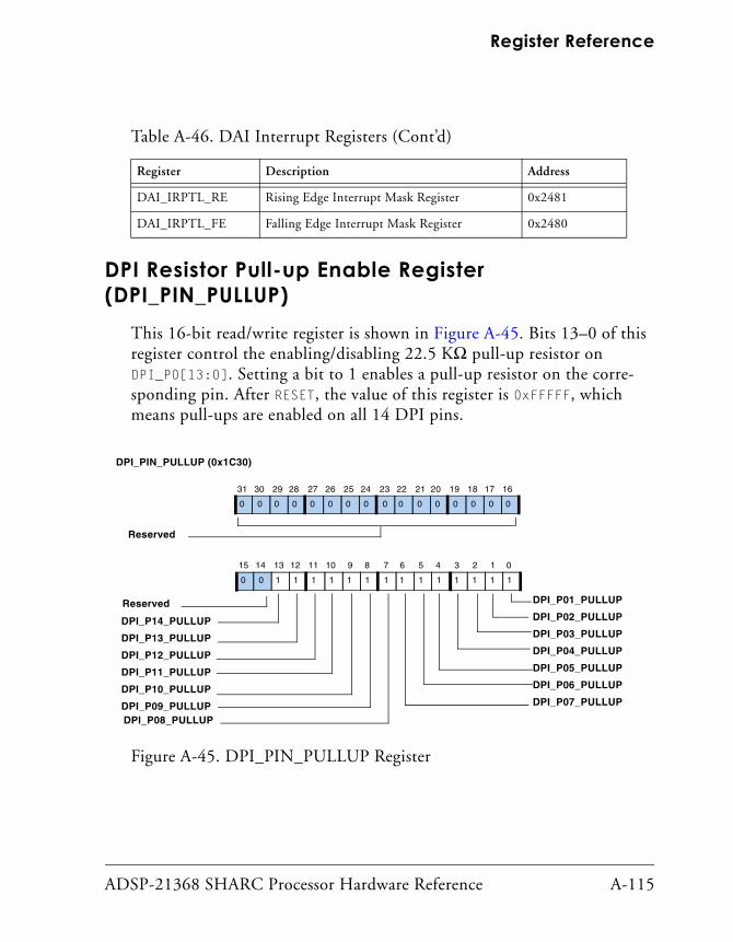
ADSP-21368 SHARC Processor Hardware Reference A-115
Register Reference
DPI Resistor Pull-up Enable Register (DPI_PIN_PULLUP)
This 16-bit read/write register is shown in Figure A-45. Bits 13–0 of this register control the enabling/disabling 22.5 KΩ pull-up resistor on DPI_P0[13:0]. Setting a bit to 1 enables a pull-up resistor on the corre-sponding pin. After RESET, the value of this register is 0xFFFFF, which means pull-ups are enabled on all 14 DPI pins.
DAI_IRPTL_RE Rising Edge Interrupt Mask Register 0x2481
DAI_IRPTL_FE Falling Edge Interrupt Mask Register 0x2480
Figure A-45. DPI_PIN_PULLUP Register
Table A-46. DAI Interrupt Registers (Cont’d)
Register Description Address
15 14 13 12 11 10 9 8 7 6 5 4 3 2 1 0
10 0 1 1 1 1 1 1 1 1 1 1 1 1 1
DPI_P14_PULLUP
DPI_P13_PULLUP
DPI_P12_PULLUP
DPI_P01_PULLUP
DPI_P02_PULLUP
DPI_P03_PULLUP
DPI_P04_PULLUP
DPI_P05_PULLUP
DPI_P06_PULLUPDPI_P11_PULLUP
DPI_P10_PULLUP
DPI_P09_PULLUP DPI_P07_PULLUP
DPI_P08_PULLUP
DPI_PIN_PULLUP (0x1C30)
31 30 29 28 27 26 25 24 23 22 21 20 19 18 17 16
00 0 0 0 0 0 0 0 0 0 0 0 0 0 0
Reserved
Reserved

DAI/DPI Registers
A-116 ADSP-21368 SHARC Processor Hardware Reference
DPI Pin Buffer Status Register (DPI_PIN_STAT)This 16-bit, read-only register is shown in Figure A-46. Bits 13–0 of this register indicate the status of DPI_PB[14:1]. Reads from bits 15–14 always return 0. This register is updated at one-half the core clock rate.
DPI Interrupt Controller RegistersThe digital peripheral interface (DPI) also has an interrupt controller, similar to that in the DAI. All of these interrupts are combined into a sin-gle interrupt, namely DPI_INT. The DPI_IRPTL register located at address 0x1C32, contains the status on individual interrupts. Apart from the DPI_IRPTL register, there are two additional registers, DPI_IRPTL_RE and DPI_IRPTL_FE that are used for interrupt latching.
Figure A-46. DPI_PIN_STAT Register
15 14 13 12 11 10 9 8 7 6 5 4 3 2 1 0
10 0 1 1 1 1 1 1 1 1 1 1 1 1 1
DPI_PB14DPI_PB13
DPI_PB12
DPI_PB01
DPI_PB02
DPI_PB03
DPI_PB04
DPI_PB05
DPI_PB06
DPI_PB11
DPI_PB10
DPI_PB09 DPI_PB07DPI_PB08
DPI_PIN_STAT (0x1C31)
31 30 29 28 27 26 25 24 23 22 21 20 19 18 17 16
00 0 0 0 0 0 0 0 0 0 0 0 0 0 0
Reserved
Reserved
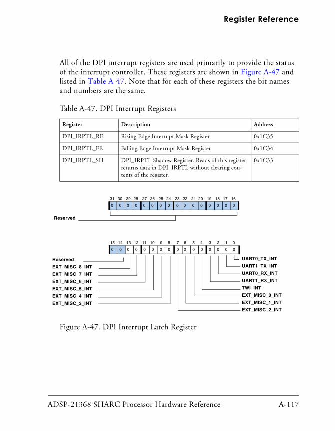
ADSP-21368 SHARC Processor Hardware Reference A-117
Register Reference
All of the DPI interrupt registers are used primarily to provide the status of the interrupt controller. These registers are shown in Figure A-47 and listed in Table A-47. Note that for each of these registers the bit names and numbers are the same.
Table A-47. DPI Interrupt Registers
Register Description Address
DPI_IRPTL_RE Rising Edge Interrupt Mask Register 0x1C35
DPI_IRPTL_FE Falling Edge Interrupt Mask Register 0x1C34
DPI_IRPTL_SH DPI_IRPTL Shadow Register. Reads of this register returns data in DPI_IRPTL without clearing con-tents of the register.
0x1C33
Figure A-47. DPI Interrupt Latch Register
15 14 13 12 11 10 9 8 7 6 5 4 3 2 1 0
00 0 0 0 0 0 0 0 0 0 0 0 0 0 0
EXT_MISC_8_INT
EXT_MISC_7_INT
EXT_MISC_6_INT
EXT_MISC_5_INT
EXT_MISC_3_INT
UART0_TX_INT
UART1_TX_INT
UART1_RX_INT
UART0_RX_INT
EXT_MISC_1_INT
TWI_INT
EXT_MISC_0_INT
EXT_MISC_2_INT
EXT_MISC_4_INT
Reserved
31 30 29 28 27 26 25 24 23 22 21 20 19 18 17 16
00 0 0 0 0 0 0 0 0 0 0 0 0 0 0
Reserved
UART Control and Status Registers
A-118 ADSP-21368 SHARC Processor Hardware Reference
UART Control and Status RegistersThe processor provides a set of PC-style, industry-standard control and status registers for each UART. These memory-mapped registers (MMRs) are byte-wide registers that are mapped as half-words with the most signif-icant byte zero-filled. Transmit and receive channels are buffered. The UARTxTHR register buffers the transmit shift register (UARTxTSR) and the UARTxRBR register buffers the receive shift register (UARTxLSR). The shift registers are not directly accessible by software.
Line Control Registers (UARTxLCR)The UART line control registers (UARTxLCR, shown in Figure A-48) con-trol the format of received and transmitted character frames. The UARTSB bit functions even when the UART clock is disabled. Since the transmit pin normally drives high, it can be used as a flag out pin, if the UART is not used. In 9-bit mode, the word length is always 8 and the 9th bit is transmitted instead of the parity bit.

ADSP-21368 SHARC Processor Hardware Reference A-119
Register Reference
Figure A-48. UART Line Control Registers
15 14 13 12 11 10 8 7 6 5 4 3 2 1 0
00 0 0 0 0 0 0 0 0 0 0 0 0 0 0
Reserved UARTWLSWord Length Select00=5-bit word(UARTWLS5)01=6-bit word(UARTWLS6)10=7-bit word(UARTWLS7)11=8-bit word(UARTWLS8)
UARTSTBStop Bits1=2 stop bits for non-5-bit word length or 1 1/2 stop bits for 5-bit word length0=1 stop bit
UARTSB
Stick ParityForces parity to defined value if set and PEN = 11=Parity transmitted and checked as 00=Parity transmitted and checked as 1
UARTSTP
UARTPENParity Enable1=Transmit and check parity0=Parity not transmitted or checkedUARTEPS
Set Break1=Force Tx pin to 00=No force
9
UARTDLABDivisor Latch Access1=Enable access to UARTxDLL and UARTxDLH0=Enable access to UARTxTHR, UARTxRBR, and UART_IER
Even Parity Select1=Even parity0=Odd parity when PEN = 1 and STP = 0
UART0LCR (0x3C03)UART1LCR (0x4003)

UART Control and Status Registers
A-120 ADSP-21368 SHARC Processor Hardware Reference
Line Status Registers (UARTxLSR)The UART line status registers (UARTxLSR) contain UART status informa-tion as shown in Figure A-49. There are also shadow registers, UARTxLSRSH, with the following addresses: UART0LSRSH (0x3C0A) and UART1LSRSH (0x400A). These registers allow programs to read the contents of the corresponding main register without affecting the status the UART.
Figure A-49. UART Line Status Registers
15 14 13 12 11 10 8 7 6 5 4 3 2 1 0
00 0 0 0 0 0 0 0 0 0 0 0 0 0 0
Reserved UARTDRData Ready1=UARTx_RBR holds new data0=No new dataUARTOEOverrun Error1=UARTx_RBR overwritten before read0=No overrunUARTTHRE
Break Interrupt1=Break interrupt. This indicates Rx pin was held low for more than the max word length.0=No break interrupt
UARTBI
UARTPEParity Error1=Parity error0=No parity errorUARTFE
UARTx_THR Empty1=Empty0=Not empty
9
UARTTEMTTSR and UARTx_THR Empty1=Both empty0=Full
Framing Error1=Invalid stop bit error0=No error
UART0LSR (0x3C05)UART1LSR (0x4005)
UARTRX9D9th bit of the received charac-ter-address detect

ADSP-21368 SHARC Processor Hardware Reference A-121
Register Reference
Transmit Hold Registers (UARTxTHR) In no pack mode (default), only the lower byte of these registers is used—all other bits are zero-filled. However in pack mode, both the high and low bytes are used. The TX9D and RX9D are the 9th bit in 9-bit transmission mode. These registers are mapped to the same address as the UARTxRBR and UARTxDLL registers. A write to the UART transmit holding registers (UARTxTHR) initiates the transmit operation.
To access UARTxTHR (shown in Figure A-50), the UARTDLAB bit in UARTxLCR must be cleared. When the UARTDLAB bit is cleared, writes to this address target the UARTxTHR registers, and reads from this address return the UAR-TxRBR registers.
Figure A-50. UART Transmit Holding Registers (Packing Enabled)
31 30 29 28 27 26 25 24 23 22 21 20 19 18 17 16
00 0 0 0 0 0 0 0 0 0 0 0 0 0 0
Higher Byte
UART0THR (0x3C00)UART1THR (0x4000)
15 14 13 12 11 10 9 8 7 6 5 4 3 2 1 0
00 0 0 0 0 0 0 0 0 0 0 0 0 0 0
Lower Byte
TX9D0
TX9D1
Zero-Filled
Zero-Filled

UART Control and Status Registers
A-122 ADSP-21368 SHARC Processor Hardware Reference
Receive Buffer Registers (UARTxRBR)These read-only registers (shown in Figure A-51) are mapped to the same address as the write-only UARTxTHR and DLL registers. To access UARTxRBR, the UARTDLAB bit in the UARTxLCR register must be cleared. When the UARTDLAB bit is cleared, writes to this address target the UARTxTHR registers, while reads from this address return the UARTxRBR registers.
There are also shadow registers, UARTxRBRSH, with the following addresses: UART0RBRSH (0x3C08) and UART1RBRSH (0x4008). These registers allow programs to read the contents of the corresponding main register without affecting the status of the UART.
Figure A-51. UART Receive Buffer Registers
31 30 29 28 27 26 25 24 23 22 21 20 19 18 17 16
00 0 0 0 0 0 0 0 0 0 0 0 0 0 0
Higher Byte
UART0RBR (0x3C00)UART1RBR (0x4000)
15 14 13 12 11 10 9 8 7 6 5 4 3 2 1 0
00 0 0 0 0 0 0 0 0 0 0 0 0 0 0
Lower Byte
RX9D0
RX9D1
Zero-Filled
Zero-Filled

ADSP-21368 SHARC Processor Hardware Reference A-123
Register Reference
Interrupt Enable Registers (UARTxIER)The UART interrupt enable registers (UARTxIER) are used to enable requests for system handling of empty or full states of UART data regis-ters. Unless polling is used as a means of action, the UARTRBFIE and/or UARTTBEIE bits in these registers are normally set.
The UARTxIER register (shown in Figure A-52) is mapped to the same address as the UARTxDLH register. To access the UARTxIER register, the UARTDLAB bit in the UARTxLCR register must be cleared.
Figure A-52. UART Interrupt Enable Register
15 14 13 12 11 10 9 8 7 6 5 4 3 2 1 0
00 0 0 0 0 0 0 0 0 0 0 0 0 0 0
UARTRBFIE
UARTTBEIE
Enable Receive Buffer Full Interrupt0=No interrupt1=Generate RX interrupt if DR bit in UART_LSR is set
Enable Transmit Buffer Empty Interrupt0=No interrupt1=Generate TX interrupt if THRE bit in UART_LSR is set
UART0IER (0x3C01)UART1IER (0x4001)
UARTLSIEEnable RX Status Interrupt0=No interrupt1=Generate line status interrupt if any of UART_LSR[4–1] is set
UARTTXFIEEnable Transmit Complete Interrupt0=No interrupt1=Generate TX interrupt if TEMT bit in UART_LSR is set
UARTADIEEnable Address Detect Interrupt in 9-Bit Mode0=No interrupt1=Generate RX interrupt when address is detected in 9-bit mode

UART Control and Status Registers
A-124 ADSP-21368 SHARC Processor Hardware Reference
Interrupt Identification Registers (UARTxIIR)For legacy reasons, the UART interrupt identification registers (UARTxIIR, shown in Figure A-53) still reflect the UART interrupt status. Legacy operation may require bundling all UART interrupt sources to a single interrupt channel and servicing them all by the same software routine. This can be established by globally assigning all UART interrupts to the same interrupt priority. For more information, see “Peripheral Interrupt Priority Control Registers” on page A-164.
There are also shadow registers, UARTxIIRSH, with the following addresses: UART0IIRSH (0x3C09) and UART1IIRSH (0x4009). These registers allow programs to read the contents of the corresponding main register without affecting the status of the UART.
Figure A-53. UART Interrupt Identification Register
UARTISTATIn the order of interrupt priority, highest first.011=Receive line status. Read UART_LSR to clear interrupt request.
100=Address detect. Read RBR to clear interrupt request.
010=Receive data ready. Read UART RBR to clear interrupt request.
001=UART_THR empty. Write UART_THR or read UART_IIR to clear interrupt request, when priority = 4.
000=UART THR & TSR empty (TEMT = transmit complete). Write UART_THR or read UART_IIR to clear interrupt request, when priority = 5.
15 14 13 12 11 10 9 8 7 6 5 4 3 2 1 0
10 0 0 0 0 0 0 0 0 0 0 0 0 0 0
UART0IIR (0x3C02)UART1IIR (0x4002)
Pending Interrupt 0=Interrupt pending1=No interrupt pending
UARTNOINT

ADSP-21368 SHARC Processor Hardware Reference A-125
Register Reference
Divisor Latch Registers (UARTxDLL, UARTxDLH)The bit rate is characterized by the system clock (SCLK) and the 16-bit divisor. The divisor is split into the UART divisor latch low byte register (UARTxDLL) and the UART divisor latch high byte register (UARTxDLH), both shown in Figure A-54.
The UARTxDLL registers are mapped to the same address as the UARTxTHR and UARTxRBR registers. The UARTxDLH registers are mapped to the same address as the interrupt enable registers (UARTxIER). The UARTDLAB bit in the UARTxLCR register must be set before the UART divisor latch registers can be accessed.
Figure A-54. UART Divisor Latch Registers
Divisor Latch Low Byte[7:0]
Divisor Latch High Byte[15:8]
15 14 13 12 11 10 9 8 7 6 5 4 3 2 1 0
10 0 0 0 0 0 0 0 0 0 0 0 0 0 0
15 14 13 12 11 10 9 8 7 6 5 4 3 2 1 0
00 0 0 0 0 0 0 0 0 0 0 0 0 0 0
UART0DLL (0x3C00)UART1DLL (0x4000)
UART0DLL (0x3C01)UART1DLL (0x4001)

UART Control and Status Registers
A-126 ADSP-21368 SHARC Processor Hardware Reference
Scratch Registers (UARTxSCR)The contents of the 8-bit UART scratch registers (UARTxSCR shown in Figure A-55) is reset to 0x00. It is used for general-purpose data storage and does not control the UART hardware in any way.
Mode Registers (UARTxMODE)The UART mode registers control miscellaneous settings as shown in Figure A-56 and described Table A-48.
Figure A-55. UART Scratch Registers
Figure A-56. UART Mode Registers
Scratch[7:0]
UART0SCR (0x3C07)UART1SCR (0x4007)
15 14 13 12 11 10 9 8 7 6 5 4 3 2 1 0
00 0 0 0 0 0 0 0 0 0 0 0 0 0 0
15 14 13 12 11 10 9 8 7 6 5 4 3 2 1 0
00 0 0 0 0 0 0 0 0 0 0 0 0 0 0
UARTPACK
UARTPKSYN
Packing Enable0=No pack1=Pack
Synchronize Data Packing in Rx
UART0MODE (0x3C04)UART1MODE (0x4004)
UARTRX9Enable 9-Bit Tx in Receiver0=I/O mode1=9-bit transmission in receiver
UARTAENEnable Address Detect (if Rx9 = 1)0=Disable address detection1=Enable address detection
UARTPST0, UARTPST1Pin Status11=UART output is high in disabled state (default)00=UART output is low in disabled state01/10=UART output is three-stated in disabled state
UARTTX9Enable 9-Bit Tx in Transmitter0=I/O mode1=9-bit transmission in transmitter

ADSP-21368 SHARC Processor Hardware Reference A-127
Register Reference
UART DMA RegistersThe UART supports full-duplex DMA. Separate receive and transmit DMA channels are responsible for moving data between the peripheral and memory in this mode. The UART uses eight registers to control and provide status on DMA. The following sections provide descriptions of these registers.
Table A-48. UART Mode Register Bit Descriptions
Bit Name Description
0 UARTPACK Packing Enable. 0 = No pack1 = Packing enabled. Consecutive data words (example 0xAB and 0xCD) are packed as 0x00CD 00AB in the receiver, and 0x00CD 00AB is transmitted as two words of 0xAB and 0xCD successively from the transmitter. For more informa-tion, see “Packing Mode” on page 11-15.
1 UARTPKSYN Synchronize Data Packing in RX. When written with a 1, the next data byte goes to the lower byte position of the RBR register. This is a write-only bit and always returns zero on reads.
2 UARTTX9 Enable 9-Bit Tx in Transmitter.0 = I/O mode1 = 9-bit transmission in transmitter
3 UARTRX9 Enable 9-Bit Tx in Receiver.0 = I/O mode1 = 9-bit transmission in receiver
4 UARTAEN Enable Address Detect (If RX9 = 1). 0 = Disable address detection; all bytes are received1 = Enable address detection; interrupt and load of RBR when RX9D is set
6–5 UARTPST1, UARTPST0
Pin Status. 11 = UART output is high in disabled state (default)00 = UART output is low in disabled state01/10 = UART output is three-stated in the disabled state

UART Control and Status Registers
A-128 ADSP-21368 SHARC Processor Hardware Reference
DMA Control Registers (UARTxTXCTL, UARTxRXCTL)
Use these registers (described in Table A-49 and Table A-50) to enable DMA, DMA chaining, and to clear the transmit and receive buffers. The transmit and receive registers are read-write registers and their addresses are:
UART0TXCTL – 0x3F04
UART1TXCTL – 0x4304
UART0RXCTL – 0x3E04
UART1RXCTL – 0x4204
Table A-49. UARTxTXCTL Register Descriptions
Bit Name Description
0 UARTEN DMA Transmit Buffer Enable. When set (=1), enables the transmit buffer. When cleared, clears the transmit buffer.
1 UARTDEN DMA Enable. When set (=1), enables DMA on the speci-fied channel. When cleared, disables DMA.
2 UARTCHEN Chain Pointer DMA Enable. When set (=1), enables chain pointer DMA on the specified channel. When cleared, dis-ables chained DMA.
Table A-50. UARTxRXCTL Register Descriptions
Bit Name Description
0 UARTEN DMA Receive Buffer Enable. When set (=1), enables the receive buffer. When cleared, clears the receive buffer.
1 UARTDEN DMA Enable. When set (=1), enables DMA on the speci-fied channel. When cleared, disables DMA.
2 UARTCHEN Chain Pointer DMA Enable. When set (=1), enables chain pointer DMA on the specified channel. When cleared, dis-ables chained DMA.

ADSP-21368 SHARC Processor Hardware Reference A-129
Register Reference
DMA Status Registers (UARTxTXSTAT, UARTxRXSTAT)
These read-only registers (described in Table A-51 and Table A-52) pro-vide DMA status information and their addresses are:
UART0TXSTAT – 0x3F05
UART1TXSTAT – 0x4305
UART0RXSTAT – 0x3E05
UART1RXSTAT – 0x4205
Table A-51. UARTxTXSTAT Register Bit Descriptions
Bit Name Description
0 Reserved
1 UARTDMASTAT DMA Status. Provides DMA status.0 = TX DMA is inactive1 = TX DMA is active
2 UARTCHSTAT DMA Chaining Status. Provides DMA chaining status.0 = TX DMA chain loading is inactive1 = TX DMA chain loading is active
Table A-52. UARTxRXSTAT Register Bit Descriptions
Bit Name Description
0 UARTERRIRQ Receive Channel Error Interrupt. 0 = No error interrupt1 = Error interrupt generated due to receive error (par-ity/overrun/framing). This bit is cleared on a read of the LSR register.
1 UARTDMASTAT DMA Status. Provides DMA status.0 = RX DMA is inactive1 = RX DMA is active
2 UARTCHSTAT DMA Chaining Status. Provides DMA chaining status.0 = RX DMA chain loading is inactive1 = RX DMA chain loading is active
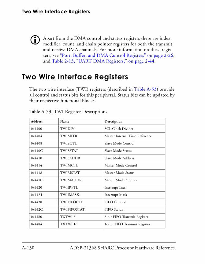
Two Wire Interface Registers
A-130 ADSP-21368 SHARC Processor Hardware Reference
Apart from the DMA control and status registers there are index, modifier, count, and chain pointer registers for both the transmit and receive DMA channels. For more information on these regis-ters, see “Port, Buffer, and DMA Control Registers” on page 2-26, and Table 2-13, “UART DMA Registers,” on page 2-44.
Two Wire Interface RegistersThe two wire interface (TWI) registers (described in Table A-53) provide all control and status bits for this peripheral. Status bits can be updated by their respective functional blocks.
Table A-53. TWI Register Descriptions
Address Name Description
0x4400 TWIDIV SCL Clock Divider
0x4404 TWIMITR Master Internal Time Reference
0x4408 TWISCTL Slave Mode Control
0x440C TWISSTAT Slave Mode Status
0x4410 TWISADDR Slave Mode Address
0x4414 TWIMCTL Master Mode Control
0x4418 TWIMSTAT Master Mode Status
0x441C TWIMADDR Master Mode Address
0x4420 TWIIRPTL Interrupt Latch
0x4424 TWIIMASK Interrupt Mask
0x4428 TWIFIFOCTL FIFO Control
0x442C TWIFIFOSTAT FIFO Status
0x4480 TXTWI 8 8-bit FIFO Transmit Register
0x4484 TXTWI 16 16-bit FIFO Transmit Register

ADSP-21368 SHARC Processor Hardware Reference A-131
Register Reference
Master Internal Time Register (TWIMITR)The TWI control register (TWIMITR, shown in Figure A-57 and described in Table A-54) is used to enable the TWI module as well as to establish a relationship between the peripheral clock (PCLK) and the TWI controller’s internally-timed events. The internal time reference is derived from PCLK using the prescaled value:
PRESCALE = fPCLK/10 MHz
0x4488 RXTWI8 8-Bit FIFO Receive Register
0x448C RXTWI16 16-Bit FIFO Receive Register
Figure A-57. Master Internal Time Register
Table A-53. TWI Register Descriptions (Cont’d)
Address Name Description
TWIMITR (0x4404)
PRESCALE
15 14 13 12 11 10 9 8 7 6 5 4 3 2 1 0
00 0 0 0 0 0 0 0 0 0 0 0 0 0 0
Reserved
TWIEN PrescaleThe number of peripheral clock (PCLK) periods used in the generation of one internal time reference.
TWI Enable0=Disable TWI1=Enable TWI master and slave mode operation

Two Wire Interface Registers
A-132 ADSP-21368 SHARC Processor Hardware Reference
Clock Divider Register (TWIDIV)During master mode operation, the SCL clock divider register (TWIDIV shown in Figure A-58 and described in Table A-55) values are used to cre-ate the high and low durations of the serial clock (SCL). Serial clock frequencies can vary from 400 KHz to less than 20 KHz. The resolution of the clock generated is 1/10 MHz or 100 ns.
Table A-54. Master Internal Time Register Bit Descriptions
Bit Name Description
0–6 PRESCALE Prescale. The number of peripheral clock (PCLK) periods used in the generation of one internal time reference. The value of PRESCALE must be set to create an internal time reference with a period of 10 MHz. This is represented as a 7-bit binary value.
7 TWIEN TWI Enable. This bit must be set for slave or master mode operation. It is recommended that this bit be set at the time PRESCALE is initialized and remain set. This guarantees accurate operation of bus busy detection logic.0 = Disable TWI1 = Enable TWI master and slave mode operation.
Figure A-58. Clock Divider Register
15 14 13 12 11 10 9 8 7 6 5 4 3 2 1 0
00 0 0 0 0 0 0 0 0 0 0 0 0 0 0
CLKLOW[7:0]
TWIDIV (0x4400)
CLKHI[7:0]

ADSP-21368 SHARC Processor Hardware Reference A-133
Register Reference
Slave Mode Control Register (TWISCTL) The TWI slave mode control register (TWISCTL) shown in Figure A-59 and described in Table A-56, controls the logic associated with slave mode operation. Settings in this register do not affect master mode operation and should not be modified to control master mode functionality.
Table A-55. Clock Divider Register Bit Descriptions
Bit Name Description
7–0 CLKLOW Clock Low. Number of internal time reference periods the serial clock (SCL) is held low. Represented as an 8-bit binary value.
15–8 CLKHI Clock High. Number of internal time reference periods the serial clock (SCL) waits before a new clock low period begins (assuming a single master). Represented as an 8-bit binary value.
Figure A-59. Slave Mode Control Register
15 14 13 12 11 10 9 8 7 6 5 4 3 2 1 0
00 0 0 0 0 0 0 0 0 0 0 0 0 0 0
TWISCTL (0x4408)
TWISEN
TWIDVAL
TWINAK
TWIGCE
TWISLEN
Slave Enable0=Slave not enabled1=Slave enabled
Slave Address Length 0=Address is a 7-bit address1=Reserved
Slave Transmit Data Valid 0=Data is for master mode transmits only1=Data is available for slave mode transmits
Not Acknowledge0=Slave RX transfer generates ACK at the conclu-sion of a data transfer1=Slave RX transfer generates a data NAK at the conclusion of a data transfer
General Call Enable0=General call address matching is not enabled1=General call address matching is enabled

Two Wire Interface Registers
A-134 ADSP-21368 SHARC Processor Hardware Reference
Table A-56. Slave Mode Control Register Bit Descriptions
Bit Name Description
0 TWISEN Slave Enable. 0 = The slave is not enabled. No attempt is made to identify a valid address. If cleared during a valid transfer, clock stretching ceases, the serial data line is released and the current byte is not acknowledged. 1 = The slave is enabled. Enabling slave and master modes of operation concurrently is allowed.
1 TWISLEN Slave Address Length.0 = Address is a 7-bit address1= Reserved. Setting this bit to 1 causes unpredictable behavior.
2 TWIDVAL Slave Transmit Data Valid. 0 = Data in the transmit FIFO is for master mode transmits and is not allowed to be used during a slave transmit, and the transmit FIFO is treated as if it is empty. 1 = Data in the transmit FIFO is available for a slave transmis-sion.
3 TWINAK Not Acknowledged.0 = Slave receive transfer generates an ACK at the conclusion of a data transfer.1 = Slave receive transfer generates a data NAK at the conclusion of a data transfer. The slave is still considered to be addressed.
4 TWIGCE General Call Enable. General call address detection is available only when slave mode is enabled. 0 = General call address matching is not enabled 1 = General call address matching is enabled. Regardless of the selected address length of slave address, a general call slave receive transfer is accepted. All status and interrupt source bits associated with transfers are updated.

ADSP-21368 SHARC Processor Hardware Reference A-135
Register Reference
Slave Address Register (TWISADDR)The TWI slave mode address register (TWISADDR, shown in Figure A-60) holds the slave mode address, which is the valid address that the slave-enabled TWI controller responds to. The TWI controller compares this value with the received address during the addressing phase of a transfer.
Slave Status Register (TWISSTAT)During and at the conclusion of slave mode transfers, the TWI slave mode status register (TWISSTAT, shown in Figure A-61) holds information on the current transfer. Generally slave mode status bits are not associated with the generation of interrupts. Master mode operation does not affect the slave mode status bits.
Figure A-60. Slave Mode Address Register
Figure A-61. Slave Mode Status Register
15 14 13 12 11 10 9 8 7 6 5 4 3 2 1 0
00 0 0 0 0 0 0 0 0 0 0 0 0 0 0
SADDR
TWISADDR (0x4410)
Slave Mode AddressValid address which this slave enabled TWIC Master responds to
15 14 13 12 11 10 9 8 7 6 5 4 3 2 1 0
00 0 0 0 0 0 0 0 0 0 0 0 0 0 0 Reset = 0x0000
TWISSTAT (0x440C)
TWISDIR Slave Transfer Direction
TWIGC (General Call)

Two Wire Interface Registers
A-136 ADSP-21368 SHARC Processor Hardware Reference
Master Control Register (TWIMCTL)The TWI master mode control register (TWIMCTL, shown in Figure A-62 and described in Table A-57) controls the logic associated with master mode operation. Bits in this register do not affect slave mode operation and should not be modified to control slave mode functionality.
Figure A-62. Master Mode Control Register
15 14 13 12 11 10 9 8 7 6 5 4 3 2 1 0
00 0 0 0 0 0 0 0 0 0 0 0 0 0 0
TWIMCTL (0x4414)
TWIMEN
TWIMDIR
TWISDAOVR
TWISCLOVR
TWIDCNT
TWIFAST
TWISTOP
TWIRSTART
TWIMLEN
Master Mode Enable0=Master mode is disabled1=Master mode is enabled
Master Address Length0=Master address is 7-bit1=Reserved
Master Transfer Direction0=Transfer is master transmit1=Transfer is master receive
Fast Mode0=Standard mode timing1=Fast mode timing
Issue Stop Condition0=Normal transfer operation. 1=The transfer will conclude as soon as possible
Serial Data Override0=Normal serial data operation1=Serial data output is driven to an active “zero” level
Indicates the Number of Data Bytes to Transfer
Repeat Start0=Transfer concludes with a STOP condition 1=Issue a repeat START condition at the conclusion of the current transfer
Serial Clock Override0=Normal serial clock operation1=Serial clock output is driven to an active “zero” level

ADSP-21368 SHARC Processor Hardware Reference A-137
Register Reference
Table A-57. Master Control Register Bit Descriptions
Bit Name Description
0 TWIMEN Master Mode Enable. Clears itself at the completion of a transfer. This includes transfers terminated due to errors. 0 = Master mode functionality is disabled. If MEN is cleared during operation, the transfer is aborted and all logic associated with master mode transfers are reset. Serial data and serial clock (SDA, SCL) are no longer driven. Write 1-to-clear status bits are not effected. 1 = Master mode functionality is enabled. A START condition is generated if the bus is idle.
1 TWIMLEN Master Address Length.0 = Address is 7-bit1 = Reserved. Setting this bit to one causes unpredictable behavior
2 TWIMDIR Master Transfer Direction.0 = The initiated transfer is master transmit1 = The initiated transfer is master receive
3 TWIFAST Fast Mode. 0 = Standard mode timing specifications in use1 = Fast mode timing specifications in use
4 TWISTOP Issue STOP Condition. 0 = Normal transfer operation1 = The transfer concludes as soon as possible avoiding any error conditions (as if data transfer count had been reached) and at that time the interrupt source register is updated along with any associ-ated status bits.
5 TWIRSTART Repeat START. 0 = Transfer concludes with a STOP condition 1 = Issue a repeat START condition at the conclusion of the current transfer (DCNT = 0) and begin the next transfer. The current trans-fer is concluded with updates to the appropriate status and interrupt bits. If errors occurred during the previous transfer, a repeat START does not occur. In the absence of any errors, master enable (MEN) does not clear itself on a repeat start.

Two Wire Interface Registers
A-138 ADSP-21368 SHARC Processor Hardware Reference
13–6 TWIDCNT Data Transfer Count. Indicates the number of data bytes to transfer. As each data word is transferred, the data transfer count is decre-mented. When DCNT is zero, a STOP (or restart condition) is issued. Setting DCNT to 0xFF disables the counter. In this transfer mode, data continues to be transferred until it is concluded by set-ting the STOP bit.
14 TWISDAOVR Serial Data (SDA) Override. For use when direct control of the Serial Data line is required. Normal master and slave mode operation should not require override operation. 0 = Normal serial data operation under the control of the transmit shift register and acknowledge logic1 = Serial data output is driven to an active “zero” level, overriding all other logic. This state is held until the bit location is cleared.
15 TWISCLOVR Serial Clock (SCL) Override. For use when direct control of the serial clock line is required. Normal master and slave mode operation should not require override operation. 0 = Normal serial clock operation under the control of master mode clock generation and slave mode clock stretching logic1 = Serial clock output is driven to an active “zero” level, overriding all other logic. This state is held until the bit location is cleared.
Table A-57. Master Control Register Bit Descriptions (Cont’d)
Bit Name Description

ADSP-21368 SHARC Processor Hardware Reference A-139
Register Reference
Master Address Register (TWIMADDR)During the addressing phase of a transfer, the TWI controller, with its master enabled, transmits the contents of the TWI master mode address register (TWIMADDR, shown in Figure A-63). When programming this regis-ter, omit the read/write bit. That is, only the upper 7 bits that make up the slave address should be written to this register. For example, if the slave address is 1010000X, then TWIMADDR is programmed with 1010000, which corresponds to 0x50. When sending out the address on the bus, the TWI controller appends the read/write bit as appropriate, based on the state of the MDIR bit in the master mode control register.
Figure A-63. Master Mode Address Register
15 14 13 12 11 10 9 8 7 6 5 4 3 2 1 0
00 0 0 0 0 0 0 0 0 0 0 0 0 0 0 Reset = 0x0000
TWIMADDR(0x441C)
MADDRMaster Mode Address

Two Wire Interface Registers
A-140 ADSP-21368 SHARC Processor Hardware Reference
Master Status Register (TWIMSTAT)The TWI master mode status register (TWIMSTAT, shown in Figure A-64 and described in Table A-58) holds information during master mode transfers and at their conclusions. Generally, master mode status bits are not directly associated with the generation of interrupts but offer informa-tion on the current transfer. Slave mode operation does not affect master mode status bits. This is a read-only register.
Figure A-64. Master Mode Status Register
15 14 13 12 11 10 9 8 7 6 5 4 3 2 1 0
00 0 0 0 0 0 0 0 0 0 0 0 0 0 0
TWIMSTAT (0x4418)
TWIMPROG
TWILOST
TWISCLSEN
TWIBUSY
TWISDASEN
TWIANAK
TWIDNAK
TWIWERR
TWIRERR
Master Tx in Progress0=No transfer is taking place 1=Master transfer is in progress
Lost Arbitration0=Transfer has not lost arbitration 1=Current transfer aborted
Address Not Acknowledged0=Transfer has not detected a NAK during addressing1=Transfer was aborted
Data Not Acknowledged0=Transfer has not detected a NAK 1=Transfer was aborted
Bus Busy0=The bus is free1=The bus is busy
Serial Clock Sense0=An inactive 1 is sensed on SCLK1=An active 0 is sensed on SCLK
Serial Data Sense0 =An inactive 1 is sensed on serial data line1=An active 0 is sensed on serial data line
Buffer Write Error0=Buffer write error not detected1=Transfer aborted due to receive buffer write error
Buffer Read Error0=Buffer read error not detected1=Transfer aborted due to transmit buffer read error
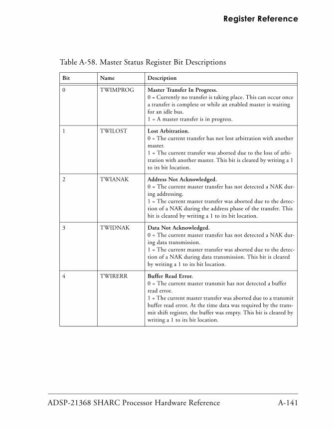
ADSP-21368 SHARC Processor Hardware Reference A-141
Register Reference
Table A-58. Master Status Register Bit Descriptions
Bit Name Description
0 TWIMPROG Master Transfer In Progress. 0 = Currently no transfer is taking place. This can occur once a transfer is complete or while an enabled master is waiting for an idle bus. 1 = A master transfer is in progress.
1 TWILOST Lost Arbitration. 0 = The current transfer has not lost arbitration with another master. 1 = The current transfer was aborted due to the loss of arbi-tration with another master. This bit is cleared by writing a 1 to its bit location.
2 TWIANAK Address Not Acknowledged. 0 = The current master transfer has not detected a NAK dur-ing addressing. 1 = The current master transfer was aborted due to the detec-tion of a NAK during the address phase of the transfer. This bit is cleared by writing a 1 to its bit location.
3 TWIDNAK Data Not Acknowledged. 0 = The current master transfer has not detected a NAK dur-ing data transmission. 1 = The current master transfer was aborted due to the detec-tion of a NAK during data transmission. This bit is cleared by writing a 1 to its bit location.
4 TWIRERR Buffer Read Error. 0 = The current master transmit has not detected a buffer read error. 1 = The current master transfer was aborted due to a transmit buffer read error. At the time data was required by the trans-mit shift register, the buffer was empty. This bit is cleared by writing a 1 to its bit location.

Two Wire Interface Registers
A-142 ADSP-21368 SHARC Processor Hardware Reference
5 TWIWERR Buffer Write Error. 0 = The current master receive has not detected a receive buffer write error. 1 = The current master transfer was aborted due to a receive buffer write error. The receive buffer and receive shift register were both full at the same time. This bit is cleared by writing a one to its bit location
6 TWISDASEN Serial Data Sense. For use when direct sensing of the serial data line is required. The register value is delayed due to the input filter (nominally 50 ns). Normal master and slave mode operation should not require this feature. 0 = An inactive “one” is currently being sensed on serial data line. 1 = An active “zero” is currently being sensed on serial data line. The source of the active driver is not known and can be internal or external.
7 TWISCLSEN Serial Clock Sense. For use when direct sensing of the serial clock line is required. The register value is delayed due to the input filter (nominally 50 ns). Normal master and slave mode operation should not require this feature. 0 = An inactive “one” is currently being sensed on SCLK. 1 = An active “zero” is currently being sensed on SCLK. The source of the active driver is not known and can be internal or external.
8 TWIBUSY Bus Busy. Indicates whether the bus is currently busy or free. This indication applies to all devices. Upon a START condi-tion, setting the register value is delayed due to the input fil-tering. Upon a STOP condition, clearing the register value occurs after time tBUF. 0 = The bus is free. The clock and data bus signals have been inactive for the appropriate bus free time. 1 = The bus is busy. Clock and/or data activity has been detected.
Table A-58. Master Status Register Bit Descriptions (Cont’d)
Bit Name Description

ADSP-21368 SHARC Processor Hardware Reference A-143
Register Reference
FIFO Control Register (TWIFIFOCTL)The TWI FIFO control register (TWIFIFOCTL, shown in Figure A-65 and described in Table A-59) affects only the FIFO and is not tied in any way with master or slave mode operation.
Figure A-65. FIFO Control Register
15 14 13 12 11 10 9 8 7 6 5 4 3 2 1 0
00 0 0 0 0 0 0 0 0 0 0 0 0 0 0
TWITXFLUSH
TWIRXFLUSH TWIRXINT2
TWITXINT2
TWIFIFOCTL (0x4428)
Receive Buffer Flush0=Normal operation1=Flush receive buffer and update the status
Transmit Buffer Flush0=Normal operation1=Flush transmit buffer and update the status
Transmit Buffer Interrupt Length0=Interrupt is set when XMTSTAT indicates one or two bytes in the FIFO are empty (01 or 00)1=Interrupt is set when XMTSTAT indicates two bytes in the FIFO are empty (00)
Receive Buffer Interrupt Length0=Interrupt is set when RCVSTAT indicates one or two bytes in the FIFO are full (01 or 11)1=Interrupt is set when RCVSTAT indicates two bytes in the FIFO are full (11)
TWIBHD
Buffer Hang Disable0 = Read of FIFO happens only when Rx FIFO has a valid byte. Write of FIFO happens only when Tx FIFO has at least one empty space.1 = Read/write happens irrespective of FIFO status
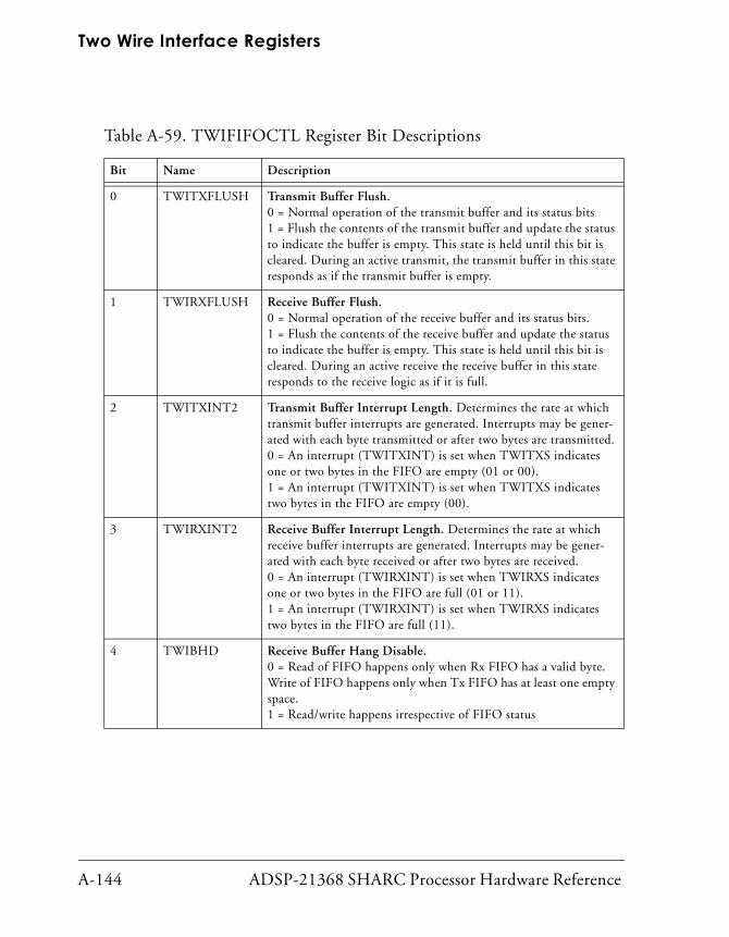
Two Wire Interface Registers
A-144 ADSP-21368 SHARC Processor Hardware Reference
Table A-59. TWIFIFOCTL Register Bit Descriptions
Bit Name Description
0 TWITXFLUSH Transmit Buffer Flush. 0 = Normal operation of the transmit buffer and its status bits 1 = Flush the contents of the transmit buffer and update the status to indicate the buffer is empty. This state is held until this bit is cleared. During an active transmit, the transmit buffer in this state responds as if the transmit buffer is empty.
1 TWIRXFLUSH Receive Buffer Flush. 0 = Normal operation of the receive buffer and its status bits. 1 = Flush the contents of the receive buffer and update the status to indicate the buffer is empty. This state is held until this bit is cleared. During an active receive the receive buffer in this state responds to the receive logic as if it is full.
2 TWITXINT2 Transmit Buffer Interrupt Length. Determines the rate at which transmit buffer interrupts are generated. Interrupts may be gener-ated with each byte transmitted or after two bytes are transmitted. 0 = An interrupt (TWITXINT) is set when TWITXS indicates one or two bytes in the FIFO are empty (01 or 00). 1 = An interrupt (TWITXINT) is set when TWITXS indicates two bytes in the FIFO are empty (00).
3 TWIRXINT2 Receive Buffer Interrupt Length. Determines the rate at which receive buffer interrupts are generated. Interrupts may be gener-ated with each byte received or after two bytes are received. 0 = An interrupt (TWIRXINT) is set when TWIRXS indicates one or two bytes in the FIFO are full (01 or 11). 1 = An interrupt (TWIRXINT) is set when TWIRXS indicates two bytes in the FIFO are full (11).
4 TWIBHD Receive Buffer Hang Disable.0 = Read of FIFO happens only when Rx FIFO has a valid byte.Write of FIFO happens only when Tx FIFO has at least one empty space.1 = Read/write happens irrespective of FIFO status

ADSP-21368 SHARC Processor Hardware Reference A-145
Register Reference
FIFO Status Register (TWIFIFOSTAT)The fields in the TWI FIFO status register (TWIFIFOSTAT, shown in Figure A-66 and described in Table A-60) indicate the state of the FIFO buffers’ receive and transmit contents. The FIFO buffers do not discrimi-nate between master data and slave data. By using the status and control bits provided, the FIFO can be managed to allow simultaneous master and slave operation. All bits in this register are read-only.
Figure A-66. FIFO Status Register
15 14 13 12 11 10 9 8 7 6 5 4 3 2 1 0
00 0 0 0 0 0 0 0 0 0 0 0 0 0 0
TWITXSTWIRXS
TWIFIFOSTAT (0x442C)
Receive FIFO Status00=FIFO is empty 01=FIFO contains one byte of data11=FIFO is full and contains two bytes of data10=Illegal
Transmit FIFO Status00=FIFO is empty01=FIFO contains one byte of data11=FIFO is full and contains two bytes of data10=Illegal
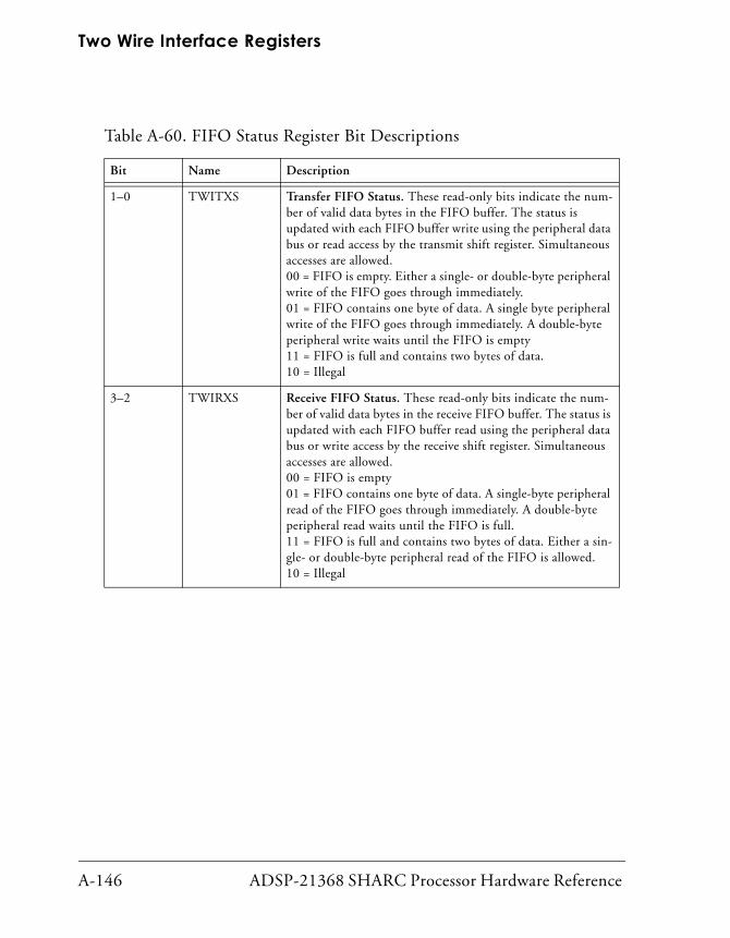
Two Wire Interface Registers
A-146 ADSP-21368 SHARC Processor Hardware Reference
Table A-60. FIFO Status Register Bit Descriptions
Bit Name Description
1–0 TWITXS Transfer FIFO Status. These read-only bits indicate the num-ber of valid data bytes in the FIFO buffer. The status is updated with each FIFO buffer write using the peripheral data bus or read access by the transmit shift register. Simultaneous accesses are allowed. 00 = FIFO is empty. Either a single- or double-byte peripheral write of the FIFO goes through immediately. 01 = FIFO contains one byte of data. A single byte peripheral write of the FIFO goes through immediately. A double-byte peripheral write waits until the FIFO is empty11 = FIFO is full and contains two bytes of data. 10 = Illegal
3–2 TWIRXS Receive FIFO Status. These read-only bits indicate the num-ber of valid data bytes in the receive FIFO buffer. The status is updated with each FIFO buffer read using the peripheral data bus or write access by the receive shift register. Simultaneous accesses are allowed. 00 = FIFO is empty 01 = FIFO contains one byte of data. A single-byte peripheral read of the FIFO goes through immediately. A double-byte peripheral read waits until the FIFO is full. 11 = FIFO is full and contains two bytes of data. Either a sin-gle- or double-byte peripheral read of the FIFO is allowed. 10 = Illegal

ADSP-21368 SHARC Processor Hardware Reference A-147
Register Reference
Interrupt Source Register (TWIIRPTL)The TWI interrupt source register (TWIIRPTL, shown in Figure A-67 and described in Table A-61) contains information about functional areas requiring servicing. Many of the bits serve as an indicator to further read and service various status registers. After servicing the interrupt source associated with a bit, the user must clear that interrupt source bit. All bits are sticky and W1C.
Figure A-67. Interrupt Source Register
15 14 13 12 11 10 9 8 7 6 5 4 3 2 1 0
00 0 0 0 0 0 0 0 0 0 0 0 0 0 0
TWISINIT
TWISCOMP
TWISERR
TWISOVF
TWIRXINT
TWITXINT
TWIIRPTL (0x4420)
TWIMERR
TWIMCOM
Slave Transfer Initiated0=Transfer is not in progress1=Transfer in progress
Slave Transfer Complete0=Transfer not detected1=Transfer is complete
Slave Transfer Error0=No errors detected1=An error has occurred
Slave Overflow0=No overflow detected1=The slave transfer complete (SCOMP) was set at the time a sub-sequent transfer has acknowledged an address phase
Receive FIFO Service0=Receive FIFO empty1=The receive FIFO buffer has one or two 8-bit loca-tions containing data to be read
Transmit FIFO Service0=Transmit FIFO is full1=The transmit FIFO buffer has one or two 8-bit locations available to be written
Master Transfer Error0=No errors detected1=A master error has occurred
Master Transfer Complete0=Transfer complete not detected1=Master transfer completed

Two Wire Interface Registers
A-148 ADSP-21368 SHARC Processor Hardware Reference
Table A-61. Interrupt Source Register Bit Descriptions
Bit Name Description
0 TWISINIT Slave Transfer Initiated. 0 = A transfer is not in progress. An address match has not occurred since the last time this bit was cleared. 1 = The slave has detected an address match and a transfer has been initiated. This bit is sticky and is cleared by writing 1 to its bit loca-tion.
1 TWISCOMP Slave Transfer Complete. 0 = The completion of a transfer not detected1 = The transfer is complete and either a stop, or a restart was detected. This bit is sticky and is cleared by writing a one to its bit location
2 TWISERR Slave Transfer Error. 0 = No errors detected. 1 = An error has occurred. A restart or stop condition has occurred during the data receive phase of a transfer. This bit is sticky and is cleared by writing a one to its bit location.
3 TWISOVF Slave Over Flow. 0 = No overflow detected. 1 = The slave transfer complete (TWISCOMP) was set at the time a subsequent transfer has acknowledged an address phase. The trans-fer continues, however, it may be difficult to delineate data of one transfer from another. This bit is sticky and is cleared by writing a one to its bit location.
4 TWIMCOM Master Transfer Complete. 0 = The completion of a transfer not detected. 1 = The initiated master transfer is complete. In the absence of a repeat start, the bus is released. This bit is sticky and is cleared by writing a 1 to its bit location.
5 TWIMERR Master Transfer Error. 0 = No errors detected. 1 = A master error occurred. The conditions surrounding the error are indicated by the master status register (TWIMSTAT). This bit is sticky and is cleared by writing a 1 to its bit location.

ADSP-21368 SHARC Processor Hardware Reference A-149
Register Reference
6 TWITXINT Transmit FIFO Service. 0 = No errors detected. 1 = The transmit FIFO buffer has one or two 8-bit locations avail-able to be written. If TWITXINT2 is 0, this bit is set each time TWITXS is updated to either 01 or 00. If TWITXINT2 is 1, this bit is set each time TWITXS is updated to 00. This bit is sticky and is cleared by writing 1 to its bit location.
7 TWIRXINT Receive FIFO Service. 0 = No errors detected. 1 = The receive FIFO buffer has one or two 8-bit locations contain-ing data to be read. If TWIRXINT2 is 0, this bit is set each time TWIRXS is updated to either 01 or 11. If RTWIRXINT2 is 1, this bit is set each time TWIRXS is updated to 11. This bit is sticky and is cleared by writing 1 to its bit location.
Table A-61. Interrupt Source Register Bit Descriptions (Cont’d)
Bit Name Description

Two Wire Interface Registers
A-150 ADSP-21368 SHARC Processor Hardware Reference
Interrupt Enable Register (TWIIMASK)The TWI interrupt enable register (TWIIMASK, shown in Figure A-68 and described in Table A-62) enables interrupt sources to assert the interrupt output. Each enable bit corresponds with one interrupt source bit in the TWI interrupt source register (TWIIRPTL). Reading and writing the TWI interrupt enable register does not affect the contents of the TWI interrupt source register. For all bits, 0 = interrupt generation disabled and 1 = interrupt generation enabled.
Figure A-68. Interrupt Mask Register
15 14 13 12 11 10 9 8 7 6 5 4 3 2 1 0
00 0 0 0 0 0 0 0 0 0 0 0 0 0 0
TWISINIT
TWISCOMP
TWISERR
TWISOVF
TWIRXINT
TWITXINT
TWIIMASK (0x4420)
TWIMERR
TWIMCOM
Slave Transfer Initiate Interrupt Enable 1=Interrupt generation enabled0=Interrupt generation disabled
Slave Transfer Complete Interrupt Enable 1=Interrupt generation enabled0=Interrupt generation disabled
Slave Transfer Error Interrupt Enable 1=Interrupt generation enabled0=Interrupt generation disabled
Slave Overflow Interrupt Enable1=Interrupt generation enabled0=Interrupt generation disabled
Receive FIFO Service Interrupt Enable1=Interrupt generation enabled0=Interrupt generation disabled
Transmit FIFO Service Interrupt Enable1=Interrupt generation enabled0=Interrupt generation disabled
Master Transfer Complete Interrupt Enable 1=Interrupt generation enabled0=Interrupt generation disabled
Master Transfer Complete Interrupt Enable 1=Interrupt generation enabled0=Interrupt generation disabled

ADSP-21368 SHARC Processor Hardware Reference A-151
Register Reference
Table A-62. Interrupt Mask Register Bit Descriptions
Bit Name Description
0 TWISINIT Slave Transfer Initiate Interrupt Enable. 0 = The corresponding interrupt source is prevented from asserting the interrupt output.1 = The corresponding interrupt source asserts the interrupt output.
1 TWISCOMP Slave Transfer Complete Interrupt. 0 = The corresponding interrupt source is prevented from asserting the interrupt output.1 = The corresponding interrupt source asserts the interrupt output.
2 TWISERR Slave Transfer Error Interrupt. 0 = The corresponding interrupt source is prevented from asserting the interrupt output.1 = The corresponding interrupt source asserts the interrupt output.
3 TWISOVF Slave Over Flow Interrupt Enable.0 = The corresponding interrupt source is prevented from asserting the interrupt output.1 = The corresponding interrupt source asserts the interrupt output.
4 TWIMCOM Master Transfer Complete Interrupt Enable. 0 = The corresponding interrupt source is prevented from asserting the interrupt output.1 = The corresponding interrupt source asserts the interrupt output.
5 TWIMERR Master Transfer Error Interrupt Enable. 0 = The corresponding interrupt source is prevented from asserting the interrupt output.1 = The corresponding interrupt source asserts the interrupt output.

Two Wire Interface Registers
A-152 ADSP-21368 SHARC Processor Hardware Reference
8-Bit Transmit FIFO Register (TXTWI8)The TWI FIFO transmit 8-bit register (TXTWI8, shown in Figure A-69) holds an 8-bit data value written into the FIFO buffer. Transmit data is entered into the corresponding transmit buffer in a first-in, first-out order. Although peripheral bus writes are 32 bits, a write access to TXTWI8 adds only one transmit data byte to the FIFO buffer. With each access, the transmit status (TWITXS) field in the TWIFIFOSTAT register is updated. If an access is performed while the FIFO buffer is full, the core waits until there is at least one byte space in the transmit FIFO buffer and then completes the write access. The bits in this register are write-only.
6 TWITXINT Transmit FIFO Service Interrupt Enable. 0 = The corresponding interrupt source is prevented from asserting the interrupt output.1 = The corresponding interrupt source asserts the interrupt output.
7 TWIRXINT Receive FIFO Service Interrupt Enable. 0 = The corresponding interrupt source is prevented from asserting the interrupt output.1 = The corresponding interrupt source asserts the interrupt output.
Figure A-69. 8-Bit Transmit FIFO Register
Table A-62. Interrupt Mask Register Bit Descriptions (Cont’d)
Bit Name Description
15 14 13 12 11 10 9 8 7 6 5 4 3 2 1 0
00 0 0 0 0 0 0 0 0 0 0 0 0 0 0
XMTDATA8[7:0] Transmit FIFO 8-Bit Data
TXTWI8 (0x4480)

ADSP-21368 SHARC Processor Hardware Reference A-153
Register Reference
16-Bit Transmit FIFO Register (TXTWI16)The TWI FIFO transmit 16-bit register (TXTWI16, shown in Figure A-70) holds a 16-bit data value written into the FIFO buffer. To reduce inter-rupt output rates and peripheral bus access times, a 16-bit transfer data access can be performed. Two data bytes can be written, effectively filling the transmit FIFO buffer with a single access. The data is written in lit-tle-endian byte order as shown in Figure A-70, where byte 0 is the first byte to be transferred and byte 1 is the second byte to be transferred.
Figure A-70. 16-Bit Transmit FIFO Register
15 14 13 12 11 10 9 8 7 6 5 4 3 2 1 0
00 0 0 0 0 0 0 0 0 0 0 0 0 0 0
XMTDATA16[7:0]
TXTWI16 (0x4484)
31 30 29 28 27 26 25 24 23 22 21 20 19 18 17 16
00 0 0 0 0 0 0 0 0 0 0 0 0 0 0
XMTDATA16[23:16]
Byte0–Transmitted first
Byte1–Transmitted second

Two Wire Interface Registers
A-154 ADSP-21368 SHARC Processor Hardware Reference
8-Bit Receive FIFO Register (RXTWI8)The TWI FIFO receive data 8-bit register (RXTWI8, shown in Figure A-71) holds an 8-bit data value read from the FIFO buffer. Receive data is read from the corresponding receive buffer in a first-in first-out order. Although peripheral bus reads are 32 bits, a read access to RXTWI8 can only access one receive data byte from the FIFO buffer. With each access, the receive status (TWIRXS) field in the TWIFIFOSTAT register is updated. If an access is performed while the FIFO buffer is empty, the core waits until there is at least one byte in the receive FIFO buffer and then completes the read access. All bits in this register are read-only.
16-Bit Receive FIFO Register (RXTWI16)The TWI FIFO receive data-double byte register (RXTWI16, shown in Figure A-72) holds a 16-bit data value read from the FIFO buffer. To reduce interrupt output rates and peripheral bus access times, a dou-ble-byte receive data access can be performed. Two data bytes can be read, effectively emptying the receive FIFO buffer with a single access. The data is read in little-endian byte order, as shown in Figure A-72, where byte 0 is the first byte received and byte 1 is the second byte received. With each access, the receive status (TWIRXS) field in the TWIFIFOSTAT register is updated to indicate it is empty. If an access is performed while the FIFO buffer is not full, the core waits until the receive FIFO buffer is full and then completes the read access. All bits in this register are read-only.
Figure A-71. 8-Bit Receive FIFO Register
15 14 13 12 11 10 9 8 7 6 5 4 3 2 1 0
00 0 0 0 0 0 0 0 0 0 0 0 0 0 0
RCVDATA8[7:0] (Receive FIFO 8-Bit Data)
RXTWI8 (0x4488)

ADSP-21368 SHARC Processor Hardware Reference A-155
Register Reference
Precision Clock Generator RegistersThe precision clock generator (PCG) consists of four identical units. Each of these units (A, B, C, and D) generates one clock (CLKA_O CLKB_O, CLKC_O or CLKD_O) and one frame sync (FSA_O, FSB_O, FSC_O or FSD_O) out-put. These units can take an input clock signal from a crystal oscillator buffer output or any of the sources in Group A of the signal routing unit (SRU).
Control Registers (PCG_CTLxx)The control registers operate exactly the same for each clock unit. The control registers enable clocks, frame syncs, and select divisors for each clock unit. These registers are shown in Figure A-73 and Figure A-74 and described in Table A-63 and Table A-64. Note that where letters and slashes appear, for example A/B/C/D, any clock unit can be chosen.
Figure A-72. 16-Bit Receive FIFO Register
15 14 13 12 11 10 9 8 7 6 5 4 3 2 1 0
00 0 0 0 0 0 0 0 0 0 0 0 0 0 0
RCVDATA16[7:0]
RXTWI16 (0x4484)
31 30 29 28 27 26 25 24 23 22 21 20 19 18 17 16
00 0 0 0 0 0 0 0 0 0 0 0 0 0 0
RCVDATA16[23:16]
Byte0
Byte1

Precision Clock Generator Registers
A-156 ADSP-21368 SHARC Processor Hardware Reference
Figure A-73. PCG_CTLx0 Registers
Table A-63. PCG_CTLx0 Register Bit Descriptions
Bit Name Description
19–0 FSxDIV Divisor for Frame Sync A/B/C/D.
29–20 FSxPHASE_HI Phase for Frame Sync A/B/C/D. This field represents the upper half of the 20-bit value for the channel A/B/C/D frame sync phase. See also FSXPHASE_LO (Bits 29-20) in PCG_CTLX_1 described on page A-157.
30 ENFSx Enable Frame Sync A/B/C/D.0 = Specified frame sync generation disabled1 = Specified frame sync generation enabled
31 ENCLKx Enable Clock A/B/C/D.0 = Specified clock generation disabled1 = Specified clock generation enabled
31 30 29 28 27 26 25 24 23 22 21 20 19 18 17 16
00 0 0 0 0 0 0 0 0 0 0 0 0 0 0
ENCLKA
15 14 13 12 11 10 9 8 7 6 5 4 3 2 1 0
00 0 0 0 0 0 0 0 0 0 0 0 0 0 0
Enable Clock A/B/C/D
Frame Sync A/B/C/D DivisorFSADIV
Frame Sync A/B/C/D Phase FSAPHASE_HI
ENFSAEnable Frame Sync A/B/C/D
PCG_CTLA0 (0x24C0)PCG_CTLB0 (0x24C2)PCG_CTLC0 (0x24C6)PCG_CTLD0 (0x24C8)
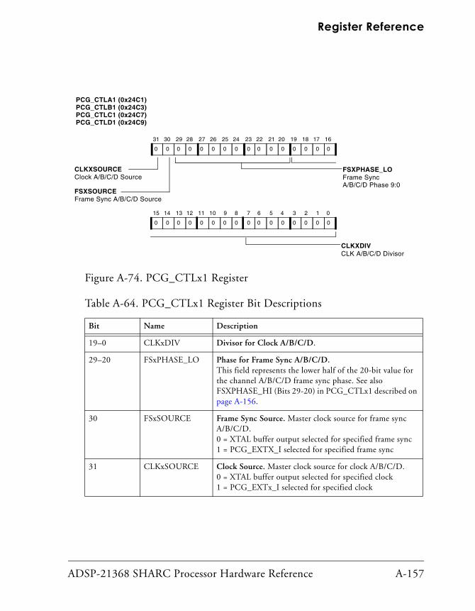
ADSP-21368 SHARC Processor Hardware Reference A-157
Register Reference
Figure A-74. PCG_CTLx1 Register
Table A-64. PCG_CTLx1 Register Bit Descriptions
Bit Name Description
19–0 CLKxDIV Divisor for Clock A/B/C/D.
29–20 FSxPHASE_LO Phase for Frame Sync A/B/C/D.This field represents the lower half of the 20-bit value for the channel A/B/C/D frame sync phase. See also FSXPHASE_HI (Bits 29-20) in PCG_CTLx1 described on page A-156.
30 FSxSOURCE Frame Sync Source. Master clock source for frame sync A/B/C/D.0 = XTAL buffer output selected for specified frame sync1 = PCG_EXTX_I selected for specified frame sync
31 CLKxSOURCE Clock Source. Master clock source for clock A/B/C/D.0 = XTAL buffer output selected for specified clock1 = PCG_EXTx_I selected for specified clock
31 30 29 28 27 26 25 24 23 22 21 20 19 18 17 16
00 0 0 0 0 0 0 0 0 0 0 0 0 0 0
CLKXSOURCE
15 14 13 12 11 10 9 8 7 6 5 4 3 2 1 0
00 0 0 0 0 0 0 0 0 0 0 0 0 0 0
Clock A/B/C/D Source
CLK A/B/C/D DivisorCLKXDIV
Frame Sync A/B/C/D Phase 9:0
FSXPHASE_LO
FSXSOURCEFrame Sync A/B/C/D Source
PCG_CTLA1 (0x24C1)PCG_CTLB1 (0x24C3)PCG_CTLC1 (0x24C7)PCG_CTLD1 (0x24C9)

Precision Clock Generator Registers
A-158 ADSP-21368 SHARC Processor Hardware Reference
PCG Pulse Width RegistersPulse width is the number of input clock periods for which the frame sync output is HIGH. Pulse width should be less than the divisor of the frame sync. The pulse width control registers are shown in Figure A-75 and Figure A-76 and described in Table A-65 and Table A-66. Note that where letters and slashes appear, for example A/B/C/D, any clock unit can be chosen.
Figure A-75. PCG_PWx Registers (in Normal Mode)
Table A-65. PCG_PWx Register Bit Descriptions (in Normal Mode)
Bit Name Description
15–0 PWFSA Pulse Width for Frame Sync A/C.Note: This is valid when not in bypass mode
31–16 PWFSB Pulse Width for Frame Sync B/D.Note: This is valid when not in bypass mode
31 30 29 28 27 26 25 24 23 22 21 20 19 18 17 16
00 0 0 0 0 0 0 0 0 0 0 0 0 0 0
15 14 13 12 11 10 9 8 7 6 5 4 3 2 1 0
00 0 0 0 0 0 0 0 0 0 0 0 0 0 0
PWFSB
Pulse Width Frame Sync A/C
PWFSA
Pulse Width Frame Sync B/D
PCG_PW (0x24C4)PCG_PW2 (0x24CA)

ADSP-21368 SHARC Processor Hardware Reference A-159
Register Reference
Figure A-76. PCG_PWx Registers (in Bypass Mode)
Table A-66. PCG_PWx Register Bit Descriptions (in Bypass Mode)
Bit Name Description
0 STROBEx One Shot Frame Sync A/C. Frame sync is a pulse with dura-tion equal to one period of the MISCA2_I signal repeating at the beginning of every frame.Note: This is valid in bypass mode only.
1 INVFSx Active Low Frame Sync Select for Frame Sync A/C. 0 = Active high frame sync1 = Active low frame sync
15–2 Reserved (In bypass mode, bits 15-2 are ignored.)
16 STROBEx One Shot Frame Sync B/D. Frame sync is a pulse with dura-tion equal to one period of the MISCA3_I signal repeating at the beginning of every frame.Note: This is valid in bypass mode only
17 INVFSx Active Low Frame Sync Select. 0 = Active high frame sync1 = Active low frame sync
31–18 Reserved (In bypass mode, bits 31–18 are ignored.)
31 30 29 28 27 26 25 24 23 22 21 20 19 18 17 16
00 0 0 0 0 0 0 0 0 0 0 0 0 0 0
Reserved
15 14 13 12 11 10 9 8 7 6 5 4 3 2 1 0
00 0 0 0 0 0 0 0 0 0 0 0 0 0 0
One Shot Frame Sync B/D
STROBEB
INVFSBActive Low Frame Sync B/D
Reserved One Shot Frame Sync A/C
STROBEA
INVFSAActive Low Frame Sync A/C
PCG_PW (0x24C4)PCG_PW2 (0x24CA)

Precision Clock Generator Registers
A-160 ADSP-21368 SHARC Processor Hardware Reference
PCG Frame Synchronization Registers (PCG_SYNCx)
These registers, shown in Figure A-77, and Figure A-78 and described in Table A-67 and Table A-68, allow programs to synchronize the clock frame syncs units with external frame syncs. For more information, see “Frame Sync” on page 13-8.
Figure A-77. PCG_SYNC Register
31 30 29 28 27 26 25 24 23 22 21 20 19 18 17 16
00 0 0 0 0 0 0 0 0 0 0 0 0 0 0
15 14 13 12 11 10 9 8 7 6 5 4 3 2 1 0
00 0 0 0 0 0 0 0 0 0 0 0 0 0 0
PCG_SYNC (0x24C5)
Enable synchronization of FSB with external LRCLK
FSB_SYNC
FSA_SOURCE_IOP
Enable frame sync A input source.0 = XTAL buffer output selected for frame sync A1 = EXT_CLKA_I selected for frame sync A
Enable synchronization of FSA with external LRCLK
FSA_SYNC
Enable synchronization of clock A with external LRCLK
CLKA_SYNCCLKA_SOURCE_IOPEnable clock A input source.0 = XTAL buffer output selected for clock A1 = EXT_CLKA_I selected for clock A
Enable synchronization of clock B with external LRCLK
CLKB_SYNC
FSB_SOURCE_IOP
CLKB_SOURCE_IOPEnable clock B input source.0 = XTAL buffer output selected for clock B1 = EXT_CLKA_I selected for clock B
Enable frame sync B input source.0 = XTAL buffer output selected for frame sync B1 = EXT_CLKA_I selected for frame sync B

ADSP-21368 SHARC Processor Hardware Reference A-161
Register Reference
Table A-67. PCG_SYNC Register Bit Descriptions
Bit Name Description
0 FSA_SYNC Enable synchronization of frame sync A with external frame sync.0 = Frame sync disabled1 = Frame sync enabled
1 CLKA_SYNC Enable synchronization of clock A with external frame sync.0 = Clock disabled1 = Clock enabled
2 CLKA_SOURCE_IOP Enable clock A input source.0 = XTAL buffer output selected for clock A1 = EXT_CLKA_I selected for clock A
3 FSA_SOURCE_IOP Enable frame sync A input source.0 = XTAL buffer output selected for frame sync A1 = EXT_CLKA_I selected for frame sync A
16 FSB_SYNC Enable synchronization of frame sync B with external frame sync.0 = Frame sync disabled1 = Frame sync enabled
17 CLKB_SYNC Enable synchronization of clock B with external frame sync.0 = Clock disabled1 = Clock enabled
18 CLKB_SOURCE_IOP Enable clock B input source.0 = XTAL buffer output selected for clock B1 = EXT_CLKA_I selected for clock B
19 FSB_SOURCE_IOP Enable frame sync B input source.0 = XTAL buffer output selected for frame sync B1 = EXT_CLKA_I selected for frame sync B

Precision Clock Generator Registers
A-162 ADSP-21368 SHARC Processor Hardware Reference
Figure A-78. PCG_SYNC2 Register
Table A-68. PCG_SYNC2 Register Bit Descriptions
Bit Name Description
0 FSC_SYNC Enable synchronization of frame sync C with external frame sync.0 = Frame sync disabled1 = Frame sync enabled
1 CLKC_SYNC Enable synchronization of clock C with external frame sync.0 = Clock disabled1 = Clock enabled
2 CLKC_SOURCE_IOP Enable clock C input source.0 = XTAL buffer output selected for clock C1 = EXT_CLKA_I selected for clock C
31 30 29 28 27 26 25 24 23 22 21 20 19 18 17 16
00 0 0 0 0 0 0 0 0 0 0 0 0 0 0
15 14 13 12 11 10 9 8 7 6 5 4 3 2 1 0
00 0 0 0 0 0 0 0 0 0 0 0 0 0 0
PCG_SYNC2 (0x24CB)
Enable synchronization of FSD with external LRCLK
FSD_SYNC
FSC_SOURCE_IOP
Enable frame sync C input source.0 = XTAL buffer output selected for frame sync C1 = EXT_CLKA_I selected for frame sync C
Enable synchronization of FSC with external LRCLK
FSC_SYNC
Enable synchronization of clock C with external LRCLK
CLKC_SYNCCLKC_SOURCE_IOPEnable clock C input source.0 = XTAL buffer output selected for clock C1 = EXT_CLKA_I selected for clock C
Enable synchronization of clock D with external LRCLK
CLKD_SYNC
FSD_SOURCE_IOP
CLKD_SOURCE_IOPEnable clock D input source.0 = XTAL buffer output selected for clock D1 = EXT_CLKA_I selected for clock D
Enable frame sync D input source.0 = XTAL buffer output selected for frame sync D1 = EXT_CLKA_I selected for frame sync D

ADSP-21368 SHARC Processor Hardware Reference A-163
Register Reference
3 FSC_SOURCE_IOP Enable frame sync C input source.0 = XTAL buffer output selected for frame sync C1 = EXT_CLKA_I selected for frame sync C
16 FSD_SYNC Enable synchronization of frame sync D with external frame sync.0 = Frame sync disabled1 = Frame sync enabled
17 CLKD_SYNC Enable synchronization of clock D with external frame sync.0 = Clock disabled1 = Clock enabled
18 CLKD_SOURCE_IOP Enable clock D input source.0 = XTAL buffer output selected for clock D1 = EXT_CLKA_I selected for clock D
19 FSD_SOURCE_IOP Enable frame sync D input source.0 = XTAL buffer output selected for frame sync D1 = EXT_CLKA_I selected for frame sync D
Table A-68. PCG_SYNC2 Register Bit Descriptions (Cont’d)
Bit Name Description

Peripheral Interrupt Priority Control Registers
A-164 ADSP-21368 SHARC Processor Hardware Reference
Peripheral Interrupt Priority Control Registers
The following sections provide descriptions of the programmable inter-rupts that are used in the ADSP-21367/8/9 and ADSP-2137x processors. For information on the interrupt registers and the interrupt vector table, see Appendix B, Interrupts.
Peripheral Interrupt Priority Control Registers (PICRx)
These registers allow programs to substitute the default interrupts for some other interrupt source. Table A-69 lists the locations to program into the IOP programmable interrupt control registers (PICR) to route an IOP interrupt source to a corresponding processor interrupt location.
Table A-69 defines the PICR bits which are programmed to select the source for each peripheral interrupt. Priority programming can be accom-plished by changing the sources for each peripheral interrupt. For example, if peripheral x needs high priority, the high priority peripheral interrupt source is set as that peripheral.

ADSP-21368 SHARC Processor Hardware Reference A-165
Register Reference
Table A-69. Peripheral Interrupt Controller Routing Table
Interrupt Name
Vector Address
Programmable Interrupt Control Register (PICR)
Default Select Value
Default Function Priority
P0I 0x2C PICR0[4:0] 0x00 DAI1I interrupt HIGHEST
P1I 0x30 PICR0[9:5] 0x01 SPIA interrupt
P2I 0x34 PICR0[14:10] 0x02 IOP GP timer-0 interrupt
P3I 0x38 PICR0[19:15] 0x03 SPORT1 interrupt
P4I 0x3C PICR0[24:20] 0x04 SPORT3 interrupt
P5I 0x40 PICR0[29:25] 0x05 SPORT5 interrupt
P6I 0x44 PICR1[4:0] 0x06 SPORT0 interrupt
P7I 0X48 PICR1[9:5] 0x07 SPORT2 interrupt
P8I 0X4C PICR1[14:10] 0x08 SPORT4 interrupt
P9I 0X50 PICR1[19 :15] 0x09 External port DMA channel0 interrupt
P10I 0X54 PICR1[24:20] 0x0A IOP GP timer-1 interrupt
P11I 0x58 PICR1[29:25] 0x0B SPORT7 interrupt
P12I 0x5C PICR2[4:0] 0x0C DAI2I interrupt
P13I 0x60 PICR2[9:5] 0x0D External port DMA channel1 interrupt
P14I 0x64 PICR2[14:10] 0x0E DPI interrupt
P15I 0x68 PICR2[19:15] 0x0F MEM/MEM interrupt
P16I 0x6C PICR2[24:20] 0x10 SPORT6 interrupt
P17I 0x70 PICR2[29:25] 0x11 IOP GP timer-2 interrupt
P18I 0x74 PICR3[4:0] 0x12 SPIB interrupt
UART0RxI 0x13 UART 0 receive interrupt
UART1RxI 0x14 UART 1 receive interrupt

Peripheral Interrupt Priority Control Registers
A-166 ADSP-21368 SHARC Processor Hardware Reference
UART0TxI 0x15 UART 0 transmit interrupt
UART1TxI 0x16 UART 0 transmit interrupt
TWII 0x17 Two wire interface interrupt
PWMI 0x18 PWM interrupt
Reserved 0x19 – 0x1E
Reserved
Logic High 0x1F Software option to set IOP interrupts
LOWEST
Table A-69. Peripheral Interrupt Controller Routing Table (Cont’d)
Interrupt Name
Vector Address
Programmable Interrupt Control Register (PICR)
Default Select Value
Default Function Priority

ADSP-21368 SHARC Processor Hardware Reference A-167
Register Reference
Peripheral Interrupt Priority0 Control Register (PICR0)
This 32-bit, read/write register controls programmable peripheral inter-rupts 0–5 and the default sources shown in Figure A-79. This register is located at address 0x2200. The reset value of this register is 0x0A418820.
Figure A-79. PICR0 Register
31 30 29 28 27 26 25 24 23 22 21 20 19 18 17 16
00 0 0 0 0 0 0 0 0 0 0 0 0 0 0
15 14 13 12 11 10 9 8 7 6 5 4 3 2 1 0
00 0 0 0 0 0 0 0 0 0 0 0 0 0 0
P5I
SPI InterruptProgrammable Interrupt 1
P1I
SPORT5 InterruptProgrammable Interrupt 5
PICR0 (0x2200)
P4ISPORT3 InterruptProgrammable Interrupt 4
P3ISPORT1 InterruptProgrammable Interrupt 3
DAI High Priority InterruptProgrammable Interrupt 0
P0I
General-Purpose IOP Timer0 InterruptProgrammable Interrupt 2
P2I
RESET=0x0A418820

Peripheral Interrupt Priority Control Registers
A-168 ADSP-21368 SHARC Processor Hardware Reference
Peripheral Interrupt Priority1 Control Register (PICR1)
This register controls programmable peripheral interrupts 6–11 and the default sources shown in Figure A-80. This 32-bit, read/write register is located at address 0x2201. The reset value of this register is 0x16A4A0E6.
Figure A-80. PICR1 Register
31 30 29 28 27 26 25 24 23 22 21 20 19 18 17 16
00 0 0 0 0 0 0 0 0 0 0 0 0 0 0
15 14 13 12 11 10 9 8 7 6 5 4 3 2 1 0
00 0 0 0 0 0 0 0 0 0 0 0 0 0 0
P11I
SPORT2 InterruptProgrammable Interrupt 7
P7I
P9IExternal Port DMA Channel 0 InterruptProgrammable Interrupt 9
SPORT0 InterruptProgrammable Interrupt 6
P6I
SPORT4 InterruptProgrammable Interrupt 8
P8I
P10I
General-Purpose I/O Timer1 InterruptProgrammable Interrupt 10
PICR1 (0x2201)
SPORT7 InterruptProgrammable Interrupt 11
RESET=0x16A4A0E6

ADSP-21368 SHARC Processor Hardware Reference A-169
Register Reference
Peripheral Interrupt Priority2 Control Register (PICR2)
This register controls programmable peripheral interrupts 12–17 as well as the default sources shown in Figure A-81. This 32-bit, read/write register is located at address 0x2202. The reset value of this register is 0x2307B9AC.
Figure A-81. PICR2 Register
31 30 29 28 27 26 25 24 23 22 21 20 19 18 17 16
00 0 0 0 0 0 0 0 0 0 0 0 0 0 0
15 14 13 12 11 10 9 8 7 6 5 4 3 2 1 0
00 0 0 0 0 0 0 0 0 0 0 0 0 0 0
External Port DMA Channel 1 InterruptProgrammable Interrupt 13
P13I
P16I
P15IMemory-to-Memory InterruptProgrammable Interrupt 15
DAI Interrupt LowProgrammable Interrupt 12
P12IP14I
P17IGeneral-Purpose I/O Timer1 InterruptProgrammable Interrupt 17
PICR2 (0x2202)
DPI InterruptProgrammable Interrupt 14
SPORT6 InterruptProgrammable Interrupt 16
RESET=0x2307B9AC

Power Management Control Register (PMCTL)
A-170 ADSP-21368 SHARC Processor Hardware Reference
Peripheral Interrupt Priority3 Control Register (PICR3)
This register controls programmable peripheral interrupt 18 as shown in Figure A-82. This 32-bit, read/write register is located at address 0x2203. The reset value of this register is 0x00000012.
Power Management Control Register (PMCTL)
The power management control register is a 32-bit, memory-mapped reg-ister. The PMCTL register’s addresses is 0x2000. This register contains bits to control phase-lock loop (PLL) multiplier and divider (both input and output) values, PLL bypass mode, and clock enabling control for peripher-als (see Figure A-83 and Table A-70). This register also contains status bits, which keep track of the status of the CLK_CFG pins (read-only).
The core can write to all bits except the read-only status bits. The DIVEN bit is a logical bit, that is, it can be set, but on reads it always responds with zero.
Figure A-82. PICR3 Register
31 30 29 28 27 26 25 24 23 22 21 20 19 18 17 16
00 0 0 0 0 0 0 0 0 0 0 0 0 0 0
15 14 13 12 11 10 9 8 7 6 5 4 3 2 1 0
00 0 0 0 0 0 0 0 0 0 0 0 0 0 0
Reserved
P18ISPI B InterruptProgrammable Interrupt 18
PICR3 (0x2203)
Reserved
RESET=0x00000012

ADSP-21368 SHARC Processor Hardware Reference A-171
Register Reference
Figure A-83. PMCTL Register
31 30 29 28 27 26 25 24 23 22 21 20 19 18 17 16
00 0 0 0 0 0 0 0 0 0 0 0 0 0 0
15 14 13 12 11 10 9 8 7 6 5 4 3 2 1 0
00 0 0 0 0 0 0 0 0 0 0 0 0 0 0
TIMEROFF
PLLBP
Timer Enable/Disable
CLKOUTEN
ReservedMux Select For CLKOUT and RESETOUT0=Mux output = RESETOUT1=Mux output = CLKOUT
DIVEN
CRAT0
PLL Clock Ratio Bit 0
PPPDN
Shut Down Clock to External Port
PLLMPLL Multiplier
SPIOFF
Shut Down Clock to SPIs
SP23POFF
Shut Down Clock to SPORT2–3
SP01OFF
Shut Down Clock to SPORT0–1
SRCOFF
Shut Down Clock to SRC, SPDIF, SRU, PCG, DAI IDP, PDAP
DTCPOFF
Shut Down Clock to DTCP
SP67OFF
PLL Divider Enable
PLLDxDivide by 2, 4, 8, or 16
INDIVInput Divider
PMCTL (0x2000)
Shut Down Clock to SPORT 6,
UART1OFF
Shut Down Clock to UART0
UART0OFFShut Down Clock to UART0
PLL Bypass
CRAT1
PLL Clock Ratio Bit 1
SDCKR
SDRAM Clock Ratio (Core Clock to SDRAM Clock)000=2, 001=2.5010=3.0, 011=3.5100=4.0101, 110, 111=Reserved
TWIOFFShut Down Clock to TWI
SDRAMOFFShut Down Clock to SDRAM ControllerPWMOFFShut Down Clock to PWM
SP45POFF
Shut Down Clock to SPORT4–5
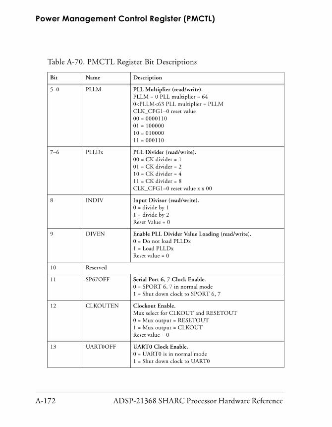
Power Management Control Register (PMCTL)
A-172 ADSP-21368 SHARC Processor Hardware Reference
Table A-70. PMCTL Register Bit Descriptions
Bit Name Description
5–0 PLLM PLL Multiplier (read/write). PLLM = 0 PLL multiplier = 640<PLLM<63 PLL multiplier = PLLMCLK_CFG1–0 reset value00 = 000011001 = 10000010 = 01000011 = 000110
7–6 PLLDx PLL Divider (read/write). 00 = CK divider = 101 = CK divider = 210 = CK divider = 411 = CK divider = 8CLK_CFG1–0 reset value x x 00
8 INDIV Input Divisor (read/write). 0 = divide by 11 = divide by 2Reset Value = 0
9 DIVEN Enable PLL Divider Value Loading (read/write).0 = Do not load PLLDx1 = Load PLLDxReset value = 0
10 Reserved
11 SP67OFF Serial Port 6, 7 Clock Enable.0 = SPORT 6, 7 in normal mode1 = Shut down clock to SPORT 6, 7
12 CLKOUTEN Clockout Enable. Mux select for CLKOUT and RESETOUT0 = Mux output = RESETOUT1 = Mux output = CLKOUTReset value = 0
13 UART0OFF UART0 Clock Enable.0 = UART0 is in normal mode1 = Shut down clock to UART0

ADSP-21368 SHARC Processor Hardware Reference A-173
Register Reference
14 UART1OFF UART1 Clock Enable.0 = UART1 is in normal mode1 = Shut down clock to UART1
15 PLLBP PLL Bypass Mode Indication. 0 = PLL is in normal mode1 = Put PLL in bypass modeReset value = 0
16 CRAT0 PLL Clock Ratio, CLKIN to CK (read only). Read only. For more detail, see the PLLM and PLLDx bit descriptions in this table.Reset value = CLK_CFG[1:0]
17 CRAT1 PLL Clock Ratio, CLKIN to CK (read only). For more detail, see the PLLM and PLLDx bit descriptions in this table.Reset value = CLK_CFG[1:0]
20–18 SDCKR SDCLK Ratio. Core clock to SDRAM clock.000 = RATIO = 2001 = RATIO = 2.5010 = RATIO = 3.0011 = RATIO = 3.5100 = RATIO = 4.0101, 110, 111 = Reserved
21 TWIOFF TWI Clock Enable.0 = TWI is in normal mode1 = Shut down clock to TWI
22 SDRAMOFF SDRAM Clock Enable.0 = SDRAM is in normal mode1 = Shut down clock to SDRAM
23 PWMOFF PWM Clock Enable.0 = PWM is in normal mode1 = Shut down clock to PWM
24 DTCPOFF DTCP Clock Enable.0 = DTCP is in normal mode1 = Shut down clock to DTCP
Table A-70. PMCTL Register Bit Descriptions (Cont’d)
Bit Name Description

Power Management Control Register (PMCTL)
A-174 ADSP-21368 SHARC Processor Hardware Reference
25 SRCOFF SRC Off.0 = SRC, SPDIF, SRU, PCG, DAI, IDP, PDAP blocks in nor-mal mode1 = Turn OFF clock to SRC, SPDIF, SRU, PCG, DAI, IDP, PDAP
26 PPPDN External Port Enable/Disable. Shuts down the clock to the asynchronous memory interface as well as SDRAM.0 = Port is in normal mode1 = Shut down clock to external portReset value = 0
27 SP01OFF SPORT0, 1 Enable/Disable. 0 = SPORTs 0–1 are in normal mode1 = Shut down clock to SPORTs 0–1Reset value = 0
28 SP23OFF SPORT2, 3 Enable/Disable. 0 = SPORTs 2–3 are in normal mode1 = Shut down clock to SPORTs 2–3Reset value = 0
29 SP45OFF SPORT4, 5 Enable/Disable. 0 = SPORTs 4–5 are in normal mode1 = Shut down clock to SPORTs 4–5Reset value = 0
30 SPIOFF SPI Enable/Disable. 0 = SPI is in normal mode1 = Shut down clock to SPINote: When this bit is set (= 1), the FLAGx pins cannot be used (via the FLAGS7–0 register bits) because the FLAGx pins are synchronized with the clock. Reset value = 0
31 TMEROFF Timer Enable/Disable. 0 = Timer is in normal mode1 = Shutdown clock to TimerReset value = 0
Table A-70. PMCTL Register Bit Descriptions (Cont’d)
Bit Name Description

ADSP-21368 SHARC Processor Hardware Reference A-175
Register Reference
Hardware Breakpoint Control RegisterThe BRKCTL register controls how breakpoints are used if bit 25, UMODE, is set. This user-accessible register, shown in Figure A-84 and Figure A-85 and described in Table A-71, is located at address 0x30025.
The register is a 32-bit, memory-mapped I/O register. The core can write into this register. The bits related to the register are the same as in the “Enhanced Emulation Status Register” on page A-179.
Note that instruction address breakpoint negates such as NEGPA1 and NEGDA1 have an effect latency of four core clock cycles.
Figure A-84. BRKCTL Register (Bits 16–31)
31 30 29 28 27 26 25 24 23 22 21 20 19 18 17 16
00 0 0 0 0 0 0 0 0 0 0 0 0 0 0
NEGIA4
UMODE
Reserved
Enable IOX Breakpoint
Enable User Mode Breakpoint1=Enable breakpoint0=Disable breakpoint
Negate Instruction Address Breakpoint #41=Enable breakpoint0=Disable breakpoint
ANDBKPAND composite breakpoints1=AND breakpoint types0=OR breakpoint types
ENBEPEnable External Port Address Break-point (See ENBPA Bit Description)
Reserved
Enable Instruction Address Break-points (See ENBPA Bit Description)
ENBIA
NEGIO1Negate I/O Address Breakpoint #11=Enable breakpoint0=Disable breakpoint
NEGEP1Negate External Address Breakpoint #11=Enable breakpoint0=Disable breakpoint
ENBPAEnable Program Memory Address Breakpoints1=Enable breakpoint0=Disable breakpoint
ENBDAEnable Data Memory Breakpoints1=Enable breakpoint0=Disable breakpoint
BRKCTL (Bits 31-16)
ENBIOY
ENBIOX
Enable IOY Breakpoint

Hardware Breakpoint Control Register
A-176 ADSP-21368 SHARC Processor Hardware Reference
Figure A-85. BRKCTL Register (Bits 0–15)
15 14 13 12 11 10 9 8 7 6 5 4 3 2 1 0
10 0 0 0 0 0 0 0 0 0 0 0 0 0 0
NEGIA3Negate Instruction Address Breakpoint #31=Enable breakpoint0=Disable breakpoint
PA1MODEPA1 Triggering Mode00=Breakpoint disabled01=WRITE access10=READ access11=Any accessNEGIA2
Negate Instruction Address Breakpoint #21=Enable breakpoint0=Disable breakpoint
NEGIA1Negate Instruction Address Breakpoint #11=Enable breakpoint0=Disable breakpoint
NEGDA2Negate DM Address Breakpoint #21=Enable breakpoint0=Disable breakpoint
NEGDA1Negate DM Address Breakpoint #11=Enable breakpoint0=Disable breakpoint
DA1MODEDA1 Triggering Mode00=Breakpoint disabled01=WRITE access10=READ access11=Any access
DA2MODEDA2 Triggering Mode00=Breakpoint disabled01=WRITE access10=READ access11=Any access
IO1MODEIO1 Triggering Mode00=Breakpoint disabled01=WRITE access10=READ access11=Any access
EP1MODEEP1 Triggering Mode00=Breakpoint disabled01=WRITE access10=READ access11=Any access
NEGPA1Negate PM Address Breakpoint #11=Enable breakpoint0=Disable breakpoint
BRKCTL (0x30025)(Bits 15-0)

ADSP-21368 SHARC Processor Hardware Reference A-177
Register Reference
Table A-71. BRKCTL Register Bit Descriptions
Bit Name Description
1–0 PA1MODE PA1Triggering Mode.00 = Breakpoint disabled01 = WRITE access10 = READ access11 = Any access
3–2 DA1MODE DA1 Triggering Mode.00 = Breakpoint disabled01 = WRITE access10 = READ access11 = Any access
5–4 DA2MODE DA2 Triggering Mode.00 = Breakpoint disabled01 = WRITE access10 = READ access11 = Any access
7–6 IO1MODE IO1 Triggering Mode.00 = Breakpoint is disabled01 = WRITE accesses only10 = READ accesses only11 = Any access
9–8 EP1MODE EP1 Triggering Mode.00 = Breakpoint disabled01 = WRITE access10 = READ access11 = Any access
10 NEGPA1 Negate Program Memory Data Address Breakpoint.Enable breakpoint events if the address is greater than the end register value OR less than the start register value. This func-tion is useful to detect index range violations in user code. 0 = Do not negate breakpoint1 = Negate breakpoint
11 NEGDA1 Negate Data Memory Address Breakpoint #1.For more information, see NEGPA1 bit description.
12 NEGDA2 Negate Data Memory Address Breakpoint #2.For more information, see NEGPA1 bit description.

Hardware Breakpoint Control Register
A-178 ADSP-21368 SHARC Processor Hardware Reference
13 NEGIA1 Negate Instruction Address Breakpoint #1.0 = Do not negate breakpoint1 = Negate breakpoint
14 NEGIA2 Negate Instruction Address Breakpoint #2.For more information, see NEGPA1 bit description.
15 NEGIA3 Negate Instruction Address Breakpoint #3.For more information, see NEGPA1 bit description.
16 NEGIA4 Negate Instruction Address Breakpoint #4.For more information, see NEGPA1 bit description.
17 NEGIO1 Negate I/O Address Breakpoint.For more information, see NEGPA1 bit description.
18 NEGEP1 Negate EP Address Breakpoint.For more information, see NEGPA1 bit description.
19 ENBPA Enable Program Memory Data Address Breakpoints.The ENB bits enable each breakpoint group. Note that when the ANDBKP bit is set, breakpoint types not involved in the generation of the effective breakpoint must be disabled. 0 = Disable breakpoints1 = Enable breakpoints
20 ENBDA Enable Data Memory Address Breakpoints.For more information, see ENBPA bit description.
21 ENBIA Enable Instruction Address Breakpoints.For more information, see ENBPA bit description.
22 Reserved
23 ENBEP Enable External Port Address Breakpoint.For more information, see ENBPA bit description.
24 ANDBKP AND Composite Breakpoints. Enables ANDing of each break-point type to generate an effective breakpoint from the com-posite breakpoint signals.0 = OR breakpoint types1 = AND breakpoint types
Table A-71. BRKCTL Register Bit Descriptions (Cont’d)
Bit Name Description

ADSP-21368 SHARC Processor Hardware Reference A-179
Register Reference
Enhanced Emulation Status RegisterThe EEMUSTAT register reports the breakpoint status of the programs that run on the ADSP-21367/8/9 and ADSP-2137x processors. This register is a memory-mapped IOP register that can be accessed by the core. The EEMUSTAT register contains two status bits that report I/O breakpoints, one each for the two I/O buses (IOX and IOY).
When a breakpoint is reached, an interrupt occurs and the breakpoint’s status bits are set. When the core returns from an interrupt, the break-point’s status bits are cleared. This register is shown in Figure A-86 and described in Table A-72.
25 UMODE User Mode Breakpoint Functionality Enable. Address Break-point 3.0 = Disable user controlled breakpoint1 = Enable user controlled breakpoint
26 ENBIOY IOY Breakpoint Enable.0 = Disable IOY breakpoint1 = Enable IOY breakpoint 0
27 ENBIOX IOX Breakpoint Enable.0 = Disable IOX breakpoint1 = Enable IOX breakpoint
31–28 Reserved
Table A-71. BRKCTL Register Bit Descriptions (Cont’d)
Bit Name Description

Enhanced Emulation Status Register
A-180 ADSP-21368 SHARC Processor Hardware Reference
Figure A-86. EEMUSTAT Register
15 14 13 12 11 10 9 8 7 6 5 4 3 2 1 0
00 0 0 0 0 0 0 0 0 0 0 0 0 0 0
OSPIDENS
EEMUIN Interrupt Enable1= EEMUIN interrupt enable0= EEMUIN interrupt disable
EEMUINENS
Operating System Processor ID Enable1=OSPID Register enable0=OSPID Register disableEEMUENSEnhanced Emulation Feature Enable Status1=Feature is enabled0=Feature is disabledEEMUINFULL
EEMUOUTFULL
EEMUIN FIFO Full Status1= EEMUIN FIFO full0= EEMUIN FIFO is not full
EEMUOUTRDY
EEMUOUT FIFO Full Status1= EEMUOUT FIFO full0= EEMUOUT FIFO is not full
EEMUOUT Valid Data Status1= EEMUOUT FIFO contains valid data0= EEMUOUT FIFO is emptyEEMUOUTIRQENEEMUOUT Interrupt Enable1= EEMUOUT interrupt enabled0= EEMUOUT interrupt disabled
STATPAProgram Memory Break-point Status1=Break occurs0=No break occursSTATDA0DM Breakpoint #0 Status1=Break occurs0=No break occursSTATDA1DM Breakpoint #1 Status1=Break occurs0=No break occursSTATIA0Instruction Breakpoint #0 Status1=Break occurs0=No break occursSTATIA1Instruction Breakpoint #1 Status1=Break occurs0=No break occursSTATIA2Instruction Breakpoint #2 Status1=Break occurs0=No break occurs
STATIA3Instruction Breakpoint #3 Status1=Break occurs0=No break occursSTATIO0I/O Breakpoint #0 Status1=Break occurs0=No break occurs
STATEPExternal Memory Breakpoint Status1=Break occurs0=No break occurs
31 30 29 28 27 26 25 24 23 22 21 20 19 18 17 16
00 0 0 0 0 0 0 0 0 0 0 0 0 0 0
STATIOYReserved IOY Memory Breakpoint Status
0= No breakpoint occurs1= Breakpoint occurs
EEMUSTAT (0x30021)

ADSP-21368 SHARC Processor Hardware Reference A-181
Register Reference
Table A-72. EEMUSTAT Register Bit Descriptions
Bit Name Description
0 STATPA Program Memory Data Breakpoint Hit.1
0 = No program memory breakpoint occurs1 = Program memory breakpoint occurs
1 STATDA0 Data Memory Breakpoint Hit.1
0 = No data memory #0 breakpoint occurs1 = Data memory #0 breakpoint occurs
2 STATDA1 Data Memory Breakpoint Hit.1
0 = No data memory #1 breakpoint occurs1 = Data memory #1 breakpoint occurs
3 STATIA0 Instruction Address Breakpoint Hit.1
0 = No instruction address #0 breakpoint occurs1 = Instruction address #0 breakpoint occurs
4 STATIA1 Instruction Address Breakpoint Hit.1
0 = No instruction address #1 breakpoint occurs1 = Instruction address #1 breakpoint occurs
5 STATIA2 Instruction Address Breakpoint Hit.1
0 = No instruction address #2 breakpoint occurs1 = Instruction address #2 breakpoint occurs
6 STATIA3 Instruction Address Breakpoint Hit.1
0 = No instruction address #3 breakpoint occurs1 = Instruction address #3 breakpoint occurs
7 STATIO I/O Address Breakpoint Hit.1
0 = No I/OX address breakpoint occurs1 = I/OX address breakpoint occurs
8 Reserved1
9 EEMUOUTIRQEN Enhanced Emulation EEMUOUT Interrupt Enable.2
0 = EEMUOUT interrupt disable1 = EEMUOUT interrupt enableNote: Interrupts are of the low priority variety
10 EEMUOUTRDY Enhanced Emulation EEMUOUT Ready.3
1 = EEMUOUT FIFO contains valid data0 = EEMUOUT FIFO is empty

Enhanced Emulation Status Register
A-182 ADSP-21368 SHARC Processor Hardware Reference
11 EEMUOUTFULL Enhanced Emulation EEMUOUT FIFO Status.3
0 = EEMUOUT FIFO is not full1 = EEMUOUT FIFO full
12 EEMUINFULL Enhanced Emulation EEMUIN Register Status.4
0 = EEMUIN register is empty1 = EEMUIN register full
13 EEMUENS Enhanced Emulation Feature Enable.4
0 = Enhanced emulation feature enable1 = Enhanced emulation feature disable
14 OSPIDENS OSPID Register Enable.4
0 = OSPID register enable1 = OSPID register disable
15 EEMUINENS EEMUIN Interrupt Enable.4
0 = EEMUIN interrupt disable1 = EEMUIN interrupt enable
16 STATIOY IOY Memory Breakpoint Status0 = No breakpoint occurs 1 = Breakpoint occurs
31–17 Reserved
1 Internal hardware sets this bit.2 This bit is set and reset by the core.3 The FIFO controller sets and resets this bit.4 Internal hardware sets and resets this bit.
Table A-72. EEMUSTAT Register Bit Descriptions (Cont’d)
Bit Name Description

ADSP-21368 SHARC Processor Hardware Reference B-1
B INTERRUPTS
This chapter provides a complete listing of the registers that are used to configure and control interrupts. Table B-2 shows all the processor inter-rupts, listed according to their bit position in the IRPTL, LIRPTL, and IMASK registers. Also shown are the addresses of the interrupt vectors. Each vector is separated by four memory locations.
Interrupt Vector TablesThe addresses in the vector table represent offsets from a base address. For an interrupt vector table in internal RAM, the base address is 0x9 0000 and for internal ROM, the base address is 0x8 0000 (see Table B-1). These are 48-bit addresses.
The interrupt name column in Table B-2 lists a mnemonic name for each interrupt as they are defined by the definitions file (def21369.h) that comes with the software development tools.
Table B-1. Interrupt Vector Table Base Address
Address1
1 These are 48-bit addresses.
Description
0x0009 0000 Internal RAM (block 0)
0x0008 0000 Internal ROM (block 0)

Interrupt Vector Tables
B-2 ADSP-21368 SHARC Processor Hardware Reference
Note that the SPI has only one interrupt for both transmit and receive operations and each serial port (SPORT) has only one interrupt for both transmit and receive.
Table B-2. Interrupt Vector Addresses
Interrupt Number
Register IRPTL/LIRPTL/MASK Bit#
Vector Address
Interrupt Name
Function
0 IRPTL 0 0x00 EMUI Emulator (read-only, non-maskable) HIGHEST PRIORITY
1 IRPTL 1 0x04 RSTI1 Reset (read-only non-maskable)
2 IRPTL 2 0x08 IICDI Illegal input condition detected
3 IRPTL 3 0x0C SOVFI Status loop or mode stack over-flow; or PC stack full
4 IRPTL 4 0x10 TMZHI Timer=0 (high priority option)
5 IRPTL 5 0x14 SPERRI SP error interrupt
6 IRPTL 6 0x18 BKPI Hardware breakpoint interrupt
7 IRPTL 7 0x1C Reserved
8 IRPTL 8 0x20 IRQ2I IRQ2I asserted
9 IRPTL 9 0x24 IRQ1I IRQ1I asserted
10 IRPTL 10 0x28 IRQ0I IRQ0I asserted
11 IRPTL 11 0x2C P0I Programmable interrupt 0(DAI1)
12 IRPTL 12 0x30 P1I2 Programmable interrupt 1 (SPIA)
13 IRPTL 13 0x34 P2I Programmable interrupt 2(GPTMR0)
14 IRPTL 14 0x38 P3I Programmable interrupt 3 (SP1)
15 IRPTL 15 0x3C P4I Programmable interrupt 4 (SP3)
16 IRPTL 16 0x40 P5I Programmable interrupt 5 (SP5)
17 LIRPTL 0 0x44 P6I Programmable interrupt 6 (SP0)
18 LIRPTL 1 0x48 P7I Programmable interrupt 7 (SP2)

ADSP-21368 SHARC Processor Hardware Reference B-3
Interrupts
19 LIRPTL 2 0x4C P8I Programmable interrupt 8 (SP4)
20 LIRPTL 3 0x50 P9I3 Programmable interrupt 9(EPDMA0)
21 LIRPTL 4 0x54 P10I Programmable interrupt 10(GPTMR1)
22 LIRPTL 5 0x58 P11I3 Programmable interrupt 11 (SP7)
23 LIRPTL 6 0x5C P12I Programmable interrupt 12(DAI2)
24 LIRPTL 7 0x60 P13I Programmable interrupt 13(EPDMA1)
25 IRPTL 17 0x64 P14I3 Programmable interrupt 14 (DPI)
26 IRPTL 18 0x68 P15I Programmable interrupt 15 (M2MI)
27 IRPTL 19 0x6C P16I Programmable interrupt 16 (SP6)
28 LIRPTL 8 0x70 P17I Programmable interrupt 17(GPTMR2)
29 LIRPTL 9 0x74 P18I3 Programmable interrupt 18 (SPIB)
30 IRPTL 20 0x78 CB7I Circular buffer 7 overflow
31 IRPTL 21 0x7C CB15I Circular buffer 15 overflow
32 IRPTL 22 0x80 TMZLI Timer=0 (low priority option)
33 IRPTL 23 0x84 FIXI Fixed-point overflow
34 IRPTL 24 0x88 FLTOI Floating-point overflow exception
35 IRPTL 25 0x8C FLTUI Floating-point underflow exception
36 IRPTL 26 0x90 FLTII Floating-point invalid exception
37 IRPTL 27 0x94 EMULI Emulator low priority interrupt
38 IRPTL 28 0x98 SFT0I User software interrupt 0
39 IRPTL 29 0x9C SFT1I User software interrupt 1
Table B-2. Interrupt Vector Addresses (Cont’d)
Interrupt Number
Register IRPTL/LIRPTL/MASK Bit#
Vector Address
Interrupt Name
Function
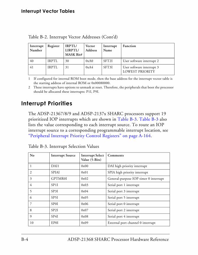
Interrupt Vector Tables
B-4 ADSP-21368 SHARC Processor Hardware Reference
Interrupt PrioritiesThe ADSP-21367/8/9 and ADSP-2137x SHARC processors support 19 prioritized IOP interrupts which are shown in Table B-3. Table B-3 also lists the value corresponding to each interrupt source. To route an IOP interrupt source to a corresponding programmable interrupt location, see “Peripheral Interrupt Priority Control Registers” on page A-164.
40 IRPTL 30 0xA0 SFT2I User software interrupt 2
41 IRPTL 31 0xA4 SFT3I User software interrupt 3 LOWEST PRIORITY
1 If configured for internal ROM boot mode, then the base address for the interrupt vector table is the starting address of internal ROM or 0x00080000.
2 These interrupts have options to unmask at reset. Therefore, the peripherals that boot the processor should be allocated these interrupts: P1I, P9I.
Table B-3. Interrupt Selection Values
No Interrupt Source Interrupt Select Value (5-Bits)
Comments
1 DAI1 0x00 DAI high priority interrupt
2 SPIAI 0x01 SPIA high priority interrupt
3 GPTMR0I 0x02 General-purpose IOP timer 0 interrupt
4 SP1I 0x03 Serial port 1 interrupt
5 SP3I 0x04 Serial port 3 interrupt
6 SP5I 0x05 Serial port 5 interrupt
7 SP0I 0x06 Serial port 0 interrupt
8 SP2I 0x07 Serial port 2 interrupt
9 SP4I 0x08 Serial port 4 interrupt
10 EP0I 0x09 External port channel 0 interrupt
Table B-2. Interrupt Vector Addresses (Cont’d)
Interrupt Number
Register IRPTL/LIRPTL/MASK Bit#
Vector Address
Interrupt Name
Function

ADSP-21368 SHARC Processor Hardware Reference B-5
Interrupts
11 GPTMR1I 0x0A Genera-purpose Timer 1 interrupt
12 SP7I 0x0B Serial port 7 interrupt
13 DAI 0x0C DAI low priority interrupt
14 EP1I 0x0D External port channel 1 interrupt
15 DPI 0x0E DPI interrupt
16 MTMDMAI 0x0F Memory-to-memory DMA interrupt
17 SP6I 0x10 Serial Port 6 interrupt
18 GPTMR2I 0x11 General-purpose timer 2 interrupt
19 SPIBI 0x12 SPI B interrupt
20 UART0RXI 0x13 UART0 RX interrupt1
21 UART1RXI 0x14 UART1 RX interrupt1
22 UART0TXI 0x15 UART0 TX interrupt1
23 UART1TXI 0x16 UART1 TX interrupt1
24 TWII 0x17 TWI interrupt1
25 PWMI 0x18 PWM interrupt1
26 Reserved 0x18–0x1E Reserved
27 LOGIC HIGH 0x1F Software option to set IOP interrupts1
1 These interrupts are not connected to the processor core interrupts by default. If these interrupts are required, then the PICR registers should be programmed explicitly. For more information, see “Peripheral Interrupt Priority Control Registers” in Appendix A, Register Reference.
Table B-3. Interrupt Selection Values (Cont’d)
No Interrupt Source Interrupt Select Value (5-Bits)
Comments

Interrupt Registers
B-6 ADSP-21368 SHARC Processor Hardware Reference
Interrupt RegistersThis section provides information on the registers that are used to config-ure and control interrupts. These registers are:
• “Interrupt Register (LIRPTL)” on page B-6
• “Interrupt Latch Register (IRPTL)” on page B-13
• “Interrupt Mask Register (IMASK)” on page B-18
• “Interrupt Mask Pointer Register (IMASKP)” on page B-22
Interrupt Register (LIRPTL)The LIRPTL register is a non-memory-mapped, universal, system register (Ureg and Sreg). The reset value for these registers is 0x0000 0000. The LIRPTL register indicates latch status, select masking, and displays mask pointers for interrupts. Figure B-1, Figure B-2, and Table B-4 provide bit definitions for the LIRPTL register.
The MSKP bits in the LIRPTL register and the entire IMASKP register are for interrupt controller use only. Modifying these bits interferes with the proper operation of the interrupt controller.
The interrupt bits 0 through 19 are programmable through the program-mable interrupt controller registers (PICRx). The descriptions provided are their default sources. For information on their optional use, see “Periph-eral Interrupt Priority Control Registers” on page A-164.

ADSP-21368 SHARC Processor Hardware Reference B-7
Interrupts
Figure B-1. LIRPTL Register (Bits 16–31)
31 30 29 28 27 26 25 24 23 22 21 20 19 18 17 16
00 0 0 0 0 0 0 0 0 0 0 0 0 0 0
P13IMSK
P12IMSKReserved Programmable Interrupt 12
Mask (DAI1 Interrupt Mask)P18IMSKPProgrammable Interrupt 18 Mask Pointer (SPI B Interrupt Mask Pointer)
P17IMSKPProgrammable Interrupt 17 Mask Pointer (General-purpose IOP Timer2 Interrupt Mask Pointer)P13MASKP
Programmable Interrupt 12 Mask Pointer (DAI1 Interrupt Mask Pointer)
P12IMSKP
P11MSKP
Programmable Interrupt 9 Mask Pointer (External Port DMA Channel 0 Interrupt Mask Pointer)
P10IMSKPProgrammable Interrupt 10 Mask Pointer (General-Purpose IOP Timer1 Interrupt Mask Pointer)P9IMSKP
P17IMSKProgrammable Interrupt 17 Mask (General-Purpose IOP Timer2 Interrupt Mask)
P18IMSKProgrammable Interrupt 18 Mask (SPI B Interrupt Mask)
P6IMSKPProgrammable Interrupt 6 Mask Pointer (SPORT0 Interrupt Mask Pointer)
P7IMSKPProgrammable Interrupt 7 Mask Pointer (SPORT2 Interrupt Mask Pointer)
P8IMSKPProgrammable Interrupt 8 Mask Pointer (SPORT4 Interrupt Mask Pointer)
LIRPTL
Programmable Interrupt 13 Mask (EPDMA1 Interrupt Mask)
Defaults in parenthesis
Programmable Interrupt 13 Mask Pointer (EPDMA1 Interrupt Mask Pointer)
Programmable Interrupt 11 Mask Pointer(SPORT7 Interrupt Mask Pointer)
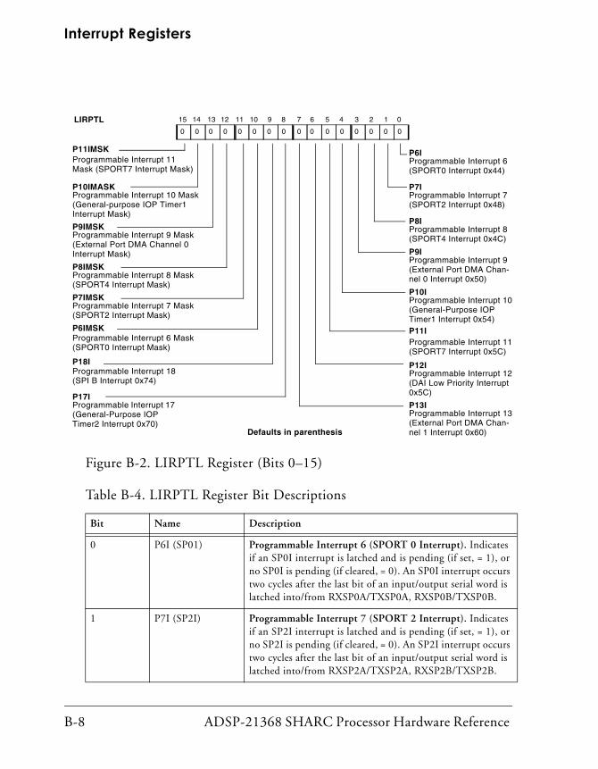
Interrupt Registers
B-8 ADSP-21368 SHARC Processor Hardware Reference
Figure B-2. LIRPTL Register (Bits 0–15)
Table B-4. LIRPTL Register Bit Descriptions
Bit Name Description
0 P6I (SP01) Programmable Interrupt 6 (SPORT 0 Interrupt). Indicates if an SP0I interrupt is latched and is pending (if set, = 1), or no SP0I is pending (if cleared, = 0). An SP0I interrupt occurs two cycles after the last bit of an input/output serial word is latched into/from RXSP0A/TXSP0A, RXSP0B/TXSP0B.
1 P7I (SP2I) Programmable Interrupt 7 (SPORT 2 Interrupt). Indicates if an SP2I interrupt is latched and is pending (if set, = 1), or no SP2I is pending (if cleared, = 0). An SP2I interrupt occurs two cycles after the last bit of an input/output serial word is latched into/from RXSP2A/TXSP2A, RXSP2B/TXSP2B.
15 14 13 12 11 10 9 8 7 6 5 4 3 2 1 0
00 0 0 0 0 0 0 0 0 0 0 0 0 0 0
P13I
P11IMSK
P9IMSK
P10IProgrammable Interrupt 10 (General-Purpose IOP Timer1 Interrupt 0x54)P11I
Programmable Interrupt 12 (DAI Low Priority Interrupt 0x5C)
P12I
P10IMASKProgrammable Interrupt 10 Mask (General-purpose IOP Timer1 Interrupt Mask)
P8IMSKProgrammable Interrupt 8 Mask (SPORT4 Interrupt Mask)
Programmable Interrupt 9 Mask (External Port DMA Channel 0 Interrupt Mask)
P7IMSKProgrammable Interrupt 7 Mask (SPORT2 Interrupt Mask)
P6IMSKProgrammable Interrupt 6 Mask (SPORT0 Interrupt Mask)
P18IProgrammable Interrupt 18 (SPI B Interrupt 0x74)
P6IProgrammable Interrupt 6 (SPORT0 Interrupt 0x44)
P7IProgrammable Interrupt 7 (SPORT2 Interrupt 0x48)
P8IProgrammable Interrupt 8 (SPORT4 Interrupt 0x4C)
P9IProgrammable Interrupt 9 (External Port DMA Chan-nel 0 Interrupt 0x50)
P17IProgrammable Interrupt 17 (General-Purpose IOP Timer2 Interrupt 0x70)
Programmable Interrupt 13 (External Port DMA Chan-nel 1 Interrupt 0x60)
LIRPTL
Defaults in parenthesis
Programmable Interrupt 11 (SPORT7 Interrupt 0x5C)
Programmable Interrupt 11 Mask (SPORT7 Interrupt Mask)

ADSP-21368 SHARC Processor Hardware Reference B-9
Interrupts
2 P8I (SP4I) Programmable Interrupt 8 (SPORT 4 Interrupt). Indicates if an SP4I interrupt is latched and is pending (if set, = 1), or no SP4I is pending (if cleared, = 0). An SP4I interrupt occurs two cycles after the last bit of an input/output serial word is latched into/from RXSP4A/TXSP4A, RXSP4B/TXSP4B.
3 P9I (EPDMA0I) Programmable Interrupt 9 (External Port DMA Channel 0 Interrupt). Indicates if an external port interrupt (EPDMA0) is latched and pending (if set, = 1), or that no external port interrupt is pending (if cleared, = 0). An external port inter-rupt occurs when the DMA block transfer has completed. This interrupt also occurs during core-driven transfers when the Tx buffer is not full or the Rx buffer is not empty.
4 P10I (GPTMR1I) Programmable Interrupt 10 (General-Purpose IOP Timer 1 Interrupt). Indicates if a GPTMR1I is latched and is pend-ing (if set, = 1), if no GPTMR1I is pending (if cleared, = 0).
5 P11I (SP7I) Programmable Interrupt 11 (SPORT 7 Interrupt). Indicates if an SP7I interrupt is latched and is pending (if set, = 1), or no SP7I is pending (if cleared, = 0). An SP7I interrupt occurs two cycles after the last bit of an input/output serial word is latched into/from RXSP7A/TXSP7A, RXSP7B/TXSP7B.
6 P12I (DAI2I) Programmable Interrupt 12 (DAI2 Interrupt). Indicates if a DAI2 interrupt is latched and is pending (if set, = 1) or no DAI2 interrupt is pending (if cleared, = 0). This is the lower priority option.
7 P13I (EPDMA1I) Programmable Interrupt 13 (External Port DMA Channel 1 Interrupt). Indicates if an external port interrupt (EPDMA1) is latched and pending (if set, = 1), or that no external port interrupt is pending (if cleared, = 0). An external port inter-rupt occurs when the DMA block transfer has completed. This interrupt also occurs during core-driven transfers when the Tx buffer is not full or the Rx buffer is not empty.
8 P17I (GPTMR2I) Programmable Interrupt 17 (General-Purpose IOP Timer 2 Interrupt). Indicates if a GPTMR2I is latched and is pend-ing (if set, = 1), or no GPTMR2I is pending (if cleared, = 0).
Table B-4. LIRPTL Register Bit Descriptions (Cont’d)
Bit Name Description

Interrupt Registers
B-10 ADSP-21368 SHARC Processor Hardware Reference
9 P18I (SPIB) Programmable Interrupt 18 (SPI B Interrupt). Indicates if an SPIB interrupt is latched and pending (if set, = 1), or no SPIBI interrupt is pending (if cleared, = 0).
10 P6IMSK (SP0IMSK)
Programmable Interrupt Mask 6 (SPORT0 Interrupt Mask). Unmasks the SP0I interrupt (if set, = 1), or masks the SP0I interrupt (if cleared, = 0).
11 P7IMSK (SP2IMSK)
Programmable Interrupt Mask 7 (SPORT2 Interrupt Mask). Unmasks the SP2I interrupt (if set, = 1), or masks the SP2I interrupt (if cleared, = 0).
12 P8IMSK (SP4IMSK)
Programmable Interrupt Mask 8 (SPORT4 Interrupt Mask). Unmasks the SP4I interrupt (if set, = 1), or masks the SP4I interrupt (if cleared, = 0).
13 P9IMSK (EPDMA0MSK)
Programmable Interrupt Mask 9 (External Port DMA Channel 0 Interrupt Mask). Unmasks the EPDMA0 inter-rupt (if set, = 1), or masks the EPDMA0 interrupt (if cleared, = 0).
14 P10IMSK (GPTMR1IMSK)
Programmable Interrupt Mask 9 (General-Purpose IOP Timer 1 Interrupt Mask). Unmasks the GPTMR1I interrupt (if set, = 1), or masks the GPTMR1I interrupt (if cleared, = 0).
15 P11IMSK Programmable Interrupt Mask 11 (SPORT7 Interrupt Mask). Unmasks the SP7I interrupt (if set, = 1), or masks the SP7I interrupt (if cleared, = 0).
16 P12IMSK(DAI2IMSK)
Programmable Interrupt Mask 12 (DAI2 Interrupt Mask). Unmasks the DAI2I (if set, = 1), or masks DAI2I (if cleared, = 0).
17 P13IMSK (EPDMA1IMSK)
Programmable Interrupt Mask 12 (External Port DMA Channel 1 Interrupt Mask). Unmasks the EPDMA1I inter-rupt (if set, = 1), or masks EPDMA1I interrupt (if set, = 0).
18 P17IMSK(GPTMR2IMSK)
Programmable Interrupt Mask 17 (General-Purpose IOP Timer 2 Interrupt Mask.) Unmasks the GPTMR2I interrupt (if set, = 1), or masks the GPTMR2I interrupt (if cleared, = 0).
Table B-4. LIRPTL Register Bit Descriptions (Cont’d)
Bit Name Description

ADSP-21368 SHARC Processor Hardware Reference B-11
Interrupts
19 P18IMSK(SPIBMSK)
Programmable Interrupt Mask 18 (SPI Interrupt Mask Sec-ondary SPI Port). Unmasks the SPIB interrupt (if set, = 1), or masks the SPIB interrupt (if cleared, = 0).
20 P6IMSKP(SP0IMSKP)
Programmable Interrupt Mask Pointer 9 (SPORT0 Inter-rupt Mask Pointer). When the processor is servicing another interrupt, this bit indicates if the SP0I interrupt is unmasked (if set, = 1), or the SP0I interrupt is masked (if cleared, = 0).
21 P7IMSKP(SP2IMSKP)
Programmable Interrupt Mask Pointer 7 (SPORT2 Inter-rupt Mask Pointer). When the processor is servicing another interrupt, this bit indicates if the SP2I interrupt is unmasked (if set, = 1), or the SP2I interrupt is masked (if cleared, = 0).
22 P8IMSKP(SP4IMSKP)
Programmable Interrupt Mask Pointer 8 (SPORT4 Inter-rupt Mask Pointer). When the processor is servicing another interrupt, this bit indicates if the SP4I interrupt is unmasked (if set, = 1), or the SP4I interrupt is masked (if cleared, = 0).
23 P9IMSKP (EPDMA0IMSKP)
Programmable Interrupt Mask Pointer 9 (External Port DMA Channel 0 Interrupt Mask Pointer). When the pro-cessor is servicing another interrupt, this bit indicates if the EPDMA0 interrupt is unmasked (if set, = 1), or masked (if cleared, = 0).
24 P10IMSKP(GPTMR1MSKP)
Programmable Interrupt Mask Pointer 10 (General-Pur-pose IOP Timer 1 Interrupt Mask Pointer).When the processor is servicing another interrupt, this bit indicates if the GPTMR1I interrupt is unmasked (if set, = 1), or the GPTMR1I interrupt is masked (if cleared, = 0).
25 P11MSKP Programmable Interrupt Mask Pointer 11 (SPORT7 Inter-rupt Mask Pointer). When the processor is servicing another interrupt, this bit indicates if the SP7I interrupt is unmasked (if set, = 1), or the SP7I interrupt is masked (if cleared, = 0).
26 P12IMSKP(DAI2IMSKP)
Programmable Interrupt Mask Pointer 12 (DAI Low Prior-ity Interrupt Mask Pointer).When the processor is servicing another interrupt, this bitindicates if the DAI2I is unmasked (if set, = 1), or masked (if cleared, = 0).
Table B-4. LIRPTL Register Bit Descriptions (Cont’d)
Bit Name Description

Interrupt Registers
B-12 ADSP-21368 SHARC Processor Hardware Reference
27 P13IMASKP (EPDMA1IMSKP)
Programmable Interrupt 13 Mask Pointer (External Port DMA Channel 1 Interrupt Mask Pointer).When the processor is servicing another interrupt, this bitindicates if the EPDMA1I is unmasked (if set, = 1) or masked (if cleared, = 0).
28 P17MSKP(GPTMR2IMSKP)
Programmable Interrupt Mask Pointer 17 (General-Pur-pose IOP Timer 2 Interrupt Mask Pointer).When the processor is servicing another interrupt, this bitindicates if the GPTMR2I interrupt is unmasked (if set, = 1), or the GPTMR2I interrupt is masked (if cleared, = 0).
29 P18MSKP(SPIBIMSKP)
Programmable Interrupt Mask Pointer 8 (SPIBI Interrupt Mask Pointer). When the processor is servicing another interrupt, this bit indicates if the SPIBI interrupt is unmasked (if set, = 1), or the SPIBI interrupt is masked (if cleared, = 0).
31–30 Reserved
Table B-4. LIRPTL Register Bit Descriptions (Cont’d)
Bit Name Description

ADSP-21368 SHARC Processor Hardware Reference B-13
Interrupts
Interrupt Latch Register (IRPTL)The IRPTL register is a non-memory-mapped, universal, system register (Ureg and Sreg). The reset value for this register is 0x0000 0000. The IRPTL register indicates latch status for interrupts. Figure B-3, Figure B-4 and Table B-5 provide bit definitions for the IRPTL register.
Figure B-3. IRPTL, IMASK, and IMASKP Registers (Bits 31–16)
31 30 29 28 27 26 25 24 23 22 21 20 19 18 17 16
00 0 0 0 0 0 0 0 0 0 0 0 0 0 0
P14I
TMZLI
P5ISFT3IUser Software Interrupt 3 (0xA4)
Timer Expired Low Priority (0x80)
CB15I
Programmable Interrupt 5 (SPORT5 Interrupt 0x40)
SFT2IUser Software Interrupt 2 (0xA0)SFT1IUser Software Interrupt 1 (0x9C)
SFT0IUser Software Interrupt 0 (0x98)
EMULIEmulator Interrupt (0x94)
FLTIIFloating-Point Invalid Operation (0x90)
Floating-Point Underflow (0x8C)FLTUI
CB7I
DAG1 Circular Buffer 15Overflow (0x7C)
FIXIFixed-Point Overflow (0x84)
FLTOIFloating-Point Overflow (0x88)
IRPTL (Bits 31-16)
DAG1 Circular Buffer 7IOverflow 0x78
P15IProgrammable Interrupt 15 (MTMDMA interrupt 0x68)P16I
Defaults in parenthesis
Programmable Interrupt 14(DPI Interrupt 0x64)
Programmable Interrupt 16(SPORT6 Interrupt 0x6C)

Interrupt Registers
B-14 ADSP-21368 SHARC Processor Hardware Reference
The interrupt latch bits 11 through 19 are programmable through the programmable interrupt controller register (PICR). The descriptions pro-vided are their default sources. For information on their optional use, see “Peripheral Interrupt Priority Control Registers” on page A-164.
Figure B-4. IRPTL, IMASK, and IMASKP Registers (Bits 15–0)
Table B-5. Interrupt Latch (IRPTL) Register Bit Descriptions
Bit Name Description
0 EMUI Emulator Interrupt. Indicates if an EMUI is latched and is pending (if set, = 1,) or no EMUI is pending (if cleared, = 0). An EMUI occurs on reset and when an external device asserts the EMU pin.
1 RSTI Reset Interrupt. Indicates if an RSTI is latched and is pending (if set, = 1), or no RSTI is pending (if cleared, = 0). An RSTI occurs on reset as an external device asserts the RESET pin.
15 14 13 12 11 10 9 8 7 6 5 4 3 2 1 0
00 0 0 0 0 0 0 0 0 0 0 0 0 0 0
Reserved
SOVFI
EMUIP4IProgrammable Interrupt 4 (SPORT 3 Interrupt 0x3C)
Stack Full/Overflow (0x0C)
Reset (Reset 0x04)
IICDI
Emulator Interrupt (Interrupt Vector Address 0x00)P3I
Programmable Interrupt 3 (SPORT 1 Interrupt 0x38)
P2IProgrammable Interrupt 2 (Gen-eral-Purpose IOP Timer 0 Interrupt 0x34)
P1IProgrammable Interrupt 1 (SPI Transmit or Receive High Priority Interrupt 0x30)
P0IProgrammable Interrupt 0 (DAI1 Interrupt 0x2C)
IRQ0IIRQ0_I Hardware Interrupt (0x28)
IRQ1_I Hardware Interrupt (0x24)IRQ1I
RSTI
Illegal Input Condition Detected (0x08)
TMZHITimer Expired High Priority (0x10)
SPERRI
Hardware BreakpointInterrupt (0x18)
IRQ2_I Hardware Interrupt (0x20)IRQ2I
BKPI
IRPTL (Bits 15-0)
Defaults in parenthesis
SP Error InterruptInterrupt (0x18)

ADSP-21368 SHARC Processor Hardware Reference B-15
Interrupts
2 IICDI Illegal Input Condition Detected Interrupt. Indicates if an IICDI is latched and is pending (if set, = 1), or no IICDI is pending (if cleared, = 0). An IICDI occurs when a true results from the logical Oring of the illegal I/O processor register access (IIRA) and unaligned 64-bit memory access bits in the STKYx registers.
3 SOVFI Stack Overflow/Full Interrupt. Indicates if a SOVFI is latched and is pending (if set, = 1), or no SOVFI is pending (if cleared, = 0). An SOVFI occurs when a stack in the program sequencer overflows or is full.
4 TMZHI Timer Expired High Priority. Indicates if a TMZHI is latched and is pending (if set, = 1), or TMZHI is not pending (if cleared, = 0). A TMZHI occurs when the timer decrements to zero. Note that this event also triggers a TMZLI. The timer operations are controlled as follows:
• The TCOUNT register contains the timer counter. The timer decrements the TCOUNT register each clock cycle.
• The TPERIOD value specifies the frequency of timer inter-rupts. The number of cycles between interrupts is TPE-RIOD + 1. The maximum value of TPERIOD is 232 – 1.
• The TIMEN bit in the MODE2 register starts and stops the timer.
Since the timer expired event (TCOUNT decrements to zero) gener-ates two interrupts, TMZHI and TMZLI, programs should unmask the timer interrupt with the desired priority and leave the other one masked.
5 SPERRI SP Error Interrupt.
6 BKPI Hardware Breakpoint Interrupt. Indicates if an BKPI is latched and is pending (if set, = 1), or no BKPI is pending (if cleared, = 0).
7 Reserved
8 IRQ2I IRQ2 Hardware Interrupt. Indicates if an IRQ2I is latched and is pending (if set, = 1), or no IRQ2I is pending (if cleared, = 0). An IRQ2I occurs when an external device asserts the FLAG2 pin config-ured as IRQ2.
Table B-5. Interrupt Latch (IRPTL) Register Bit Descriptions (Cont’d)
Bit Name Description

Interrupt Registers
B-16 ADSP-21368 SHARC Processor Hardware Reference
9 IRQ1I IRQ1 Hardware Interrupt. Indicates if an IRQ1I is latched and is pending (if set, = 1), or no IRQ1I is pending (if cleared, = 0). An IRQ1I occurs when an external device asserts the FLAG1 pin config-ured as IRQ1.
10 IRQ0I IRQ0 Hardware Interrupt. Indicates if an IRQ0I is latched and is pending (if set, = 1), or no IRQ0I is pending (if cleared, = 0). An IRQ0I occurs when an external device asserts the FLAG0 pin config-ured as IRQ0.
11 P0I(DAI1I)
Programmable Interrupt 0 (DAI High Priority Interrupt). Indicates if a DAI1I interrupt is latched and is pending (if set, = 1), or no DAI1I interrupt is pending (if cleared, = 0). This is the higher prior-ity option.
12 P1I(SPIAI)
Programmable Interrupt 1 (SPI Transmit or Receive High Priority Interrupt). Indicates if an interrupt in the primary SPIAI is latched and is pending (if set, = 1), or no interrupt is pending (if cleared, = 0). This is the higher priority option.
13 P2I (GPTMR0I)
Programmable Interrupt 2 (General-Purpose IOP Timer 0 Inter-rupt). Indicates if a GPTMR0I is latched and is pending (if set, = 1), or no GPTMR0I is pending (if cleared, = 0).
14 P3I (SP1I) Programmable Interrupt 3 (SPORT 1 Interrupt). Indicates if an SP1I interrupt is latched and is pending (if set, = 1), or no SP1I is pending (if cleared, = 0). An SP1I interrupt occurs two cycles after the last bit of an input/output serial word is latched into/from RXSP1A/TXSP1A, RXSP1B/TXSP1B.
15 P4I (SP3I) Programmable Interrupt 4 (SPORT 3 Interrupt). Indicates if an SP3I interrupt is latched and is pending (if set, = 1), or no SP3I is pending (if cleared, = 0). An SP3I interrupt occurs two cycles after the last bit of an input/output serial word is latched into/from RXSP3A/TXSP3A, RXSP3B/TXSP3B.
16 P5I (SP5I) Programmable Interrupt 5 (SPORT 5 Interrupt). Indicates if an SP5I interrupt is latched and is pending (if set, = 1), or no SP5I is pending (if cleared, = 0). An SP5I interrupt occurs two cycles after the last bit of an input/output serial word is latched into/from RXSP5A/TXSP5A, RXSP5B/TXSP5B.
Table B-5. Interrupt Latch (IRPTL) Register Bit Descriptions (Cont’d)
Bit Name Description

ADSP-21368 SHARC Processor Hardware Reference B-17
Interrupts
17 P14I (DPI) Programmable Interrupt 14. Indicates if a DPI interrupt is latched and is pending (if set, = 1), or no DPI interrupt is pending (if cleared, = 0).
18 P15I (MTMDMA)
Programmable Interrupt 15 (MTMDMA Interrupt).
19 P16I (SP6I) Programmable Interrupt 16. Indicates if an SP6I interrupt is latched and is pending (if set, = 1), or no SP6I is pending (if cleared, = 0). An SP6I interrupt occurs two cycles after the last bit of an input/output serial word is latched into/from RXSP6A/TXSP6A, RXSP6B/TXSP6B.
20 CB7I DAG1 Circular Buffer 7 Overflow Interrupt. Indicates if a CB7I is latched and is pending (if set, = 1), or no CB7I interrupt is pending (if cleared, = 0). A circular buffer overflow occurs when the DAG cir-cular buffering operation increments the I register past the end of the buffer.
21 CB15I DAG2 Circular Buffer 15 Overflow Interrupt. Indicates if a CB15I is latched and is pending (if set, = 1), or no CB15I is pending (if cleared, = 0). A circular buffer overflow occurs when the DAG circu-lar buffering operation increments the I register past the end of the buffer.
22 TMZLI Timer Expired (Low Priority) Interrupt. Indicates if a TMZLI is latched and is pending (if set, = 1), or no TMZLI is pending (if cleared, = 0). For more information, see “TMZHI” on page B-15.
23 FIXI Fixed-Point Overflow Interrupt. Indicates if a FIXI is latched and is pending (if set, = 1), or no FIXI is pending (if cleared, = 0).
24 FLTOI Floating-Point Overflow Interrupt. Indicates if a FLTOI is latched and is pending (if set, = 1), or no FLTOI is pending (if cleared, = 0).
25 FLTUI Floating-Point Underflow Interrupt. Indicates if a FLTUI is latched and is pending (if set, = 1), or no FLTUI is pending (if cleared, = 0).
26 FLTII Floating-Point Invalid Operation Interrupt. This bitindicates if a FLTII is latched and is pending (if set, = 1), or no FLTII is pending (if cleared, = 0).
Table B-5. Interrupt Latch (IRPTL) Register Bit Descriptions (Cont’d)
Bit Name Description

Interrupt Registers
B-18 ADSP-21368 SHARC Processor Hardware Reference
Interrupt Mask Register (IMASK)The IMASK register is a non-memory-mapped, universal, system register (Ureg and Sreg). The reset value for this register is 0x0000 0003. Each bit in the IMASK register corresponds to a bit with the same name in the IRPTL registers. The bits in the IMASK register unmask (enable if set, = 1), or mask (disable if cleared, = 0) the interrupts that are latched in the IRPTL register. Except for RSTI and EMUI, all interrupts are maskable.
When the IMASK register masks an interrupt, the masking disables the pro-cessor’s response to the interrupt. The IRPTL register still latches an interrupt even when masked, and the processor responds to that latched interrupt if it is later unmasked. Figure B-3, Figure B-4 and Table B-6 provide bit definitions for the IMASK register.
27 EMULI Emulator (Lower Priority) Interrupt. Indicates if an EMULI is latched and is pending (if set, = 1), or no EMULI is pending (if cleared, = 0). An EMULI occurs on reset and when an external device asserts the EMU pin. This interrupt has a lower priority than EMULI, but higher priority than software interrupts.
28 SFT0I User Software Interrupt 0. Indicates if a SFT0I is latched and is pending (if set, = 1), or no SFT0I is pending (if cleared, = 0). An SFT0I interrupt occurs when a program sets (= 1) this bit.
29 SFT1I User Software Interrupt 1. Indicates if a SFT1I is latched and is pending (if set, = 1), or no SFT1I is pending (if cleared, = 0). An SFT1I interrupt occurs when a program sets (= 1) this bit.
30 SFT2I User Software Interrupt 2. Indicates if a SFT2I is latched and is pending (if set, = 1), or no SFT2I is pending (if cleared, = 0). An SFT2I interrupt occurs when a program sets (= 1) this bit.
31 SFT3I User Software Interrupt 3. Indicates if a SFT3I is latched and is pending (if set, = 1), or no SFT3I is pending (if cleared, = 0). An SFT3I interrupt occurs when a program sets (= 1) this bit.
Table B-5. Interrupt Latch (IRPTL) Register Bit Descriptions (Cont’d)
Bit Name Description
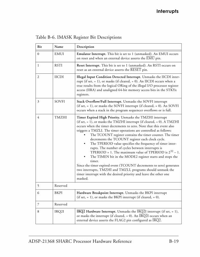
ADSP-21368 SHARC Processor Hardware Reference B-19
Interrupts
Table B-6. IMASK Register Bit Descriptions
Bit Name Description
0 EMUI Emulator Interrupt. This bit is set to 1 (unmasked). An EMUI occurs on reset and when an external device asserts the EMU pin.
1 RSTI Reset Interrupt. This bit is set to 1 (unmasked). An RSTI occurs on reset as an external device asserts the RESET pin.
2 IICDI Illegal Input Condition Detected Interrupt. Unmasks the IICDI inter-rupt (if set, = 1), or masks (if cleared, = 0). An IICDI occurs when a true results from the logical ORing of the illegal I/O processor register access (IIRA) and unaligned 64-bit memory access bits in the STKYx registers.
3 SOVFI Stack Overflow/Full Interrupt. Unmasks the SOVFI interrupt (if set, = 1), or masks the SOVFI interrupt (if cleared, = 0). An SOVFI occurs when a stack in the program sequencer overflows or is full.
4 TMZHI Timer Expired High Priority. Unmasks the TMZHI interrupt (if set, = 1), or masks the TMZHI interrupt (if cleared, = 0). A TMZHI occurs when the timer decrements to zero. Note that this event also triggers a TMZLI. The timer operations are controlled as follows:
• The TCOUNT register contains the timer counter. The timer decrements the TCOUNT register each clock cycle.
• The TPERIOD value specifies the frequency of timer inter-rupts. The number of cycles between interrupts is TPERIOD + 1. The maximum value of TPERIOD is 232 – 1.
• The TIMEN bit in the MODE2 register starts and stops the timer.
Since the timer expired event (TCOUNT decrements to zero) generates two interrupts, TMZHI and TMZLI, programs should unmask the timer interrupt with the desired priority and leave the other one masked.
5 Reserved
6 BKPI Hardware Breakpoint Interrupt. Unmasks the BKPI interrupt (if set, = 1), or masks the BKPI interrupt (if cleared, = 0).
7 Reserved
8 IRQ2I IRQ2 Hardware Interrupt. Unmasks the IRQ2I interrupt (if set, = 1), or masks the interrupt (if cleared, = 0). An IRQ2I occurs when an external device asserts the FLAG2 pin configured as IRQ2.

Interrupt Registers
B-20 ADSP-21368 SHARC Processor Hardware Reference
9 IRQ1I IRQ1 Hardware Interrupt. Unmasks the IRQ1I interrupt (if set, = 1), or masks the IRQ1I interrupt (if cleared, = 0). An IRQ1I occurs when an external device asserts the FLAG1 pin configured as IRQ1.
10 IRQ0I IRQ0 Hardware Interrupt. Unmasks the IRQ0I interrupt (if set, = 1), or masks the IRQ0I interrupt (if cleared, = 0). An IRQ0I occurs when an external device asserts the FLAG0 pin configured as IRQ0.
11 DAI1I DAI High Priority Interrupt. Unmasks the DAI1I interrupt (if set, = 1), or masks the DAI1I interrupt (if cleared, = 0). This is the higher priority option.
12 SPIAI SPI Transmit or Receive High Priority Interrupt. Unmasks the SPIAI interrupt (if set, = 1), or masks the SPIAI interrupt (if cleared, = 0). This is the higher priority option.
13 GPTMR0I General-Purpose IOP Timer 0 Interrupt. Unmasks the GPTMR0I interrupt (if set, = 1), or masks the GPTMR0I interrupt (if cleared, = 0).
14 SP1I SPORT 1 Interrupt. Unmasks the SP1I interrupt (if set, = 1), or masks the SP1I interrupt (if cleared, = 0). An SP1I interrupt occurs two cycles after the last bit of an input/output serial word is latched into/from RXSP1A/TXSP1A, or RXSP1B/TXSP1B.
15 SP3I SPORT 3 Interrupt. Unmasks the SP3I interrupt (if set, = 1), or masks the SP3I interrupt (if cleared, = 0). An SP3I interrupt occurs two cycles after the last bit of an input/output serial word is latched into/from RXSP3A/TXSP3A, or RXSP3B/TXSP3B.
16 SP5I SPORT 5 Interrupt. Unmasks the SP5I interrupt (if set, = 1), or masks the SP5I interrupt (if cleared, = 0). An SP5I interrupt occurs two cycles after the last bit of an input/output serial word is latched into/from RXSP5A/TXSP5A, or RXSP5B/TXSP5B.
17 Reserved
18 P15I Programmable Interrupt 15 (MTMDMA Interrupt).
19 Reserved
Table B-6. IMASK Register Bit Descriptions (Cont’d)
Bit Name Description

ADSP-21368 SHARC Processor Hardware Reference B-21
Interrupts
20 CB7I DAG1 Circular Buffer 7 Overflow Interrupt. Unmasks the CB7I inter-rupt (if set, = 1), or masks the CB7I interrupt (if cleared, = 0). A circu-lar buffer overflow occurs when the DAG circular buffering operation increments the I register past the end of the buffer.
21 CB15I DAG2 Circular Buffer 15 Overflow Interrupt. Unmasks the CB15I interrupt (if set, = 1), or masks the CB15I interrupt (if cleared, = 0). A circular buffer overflow occurs when the DAG circular buffering opera-tion increments the I register past the end of the buffer.
22 TMZLI Timer Expired (Low Priority) Interrupt. Unmasks the TMZLI inter-rupt (if set, = 1), or masks the TMZLI interrupt (if cleared, = 0). For more information, see “TMZHI” on page B-19.
23 FIXI Fixed-Point Overflow Interrupt. Unmasks the FIXI interrupt (if set, = 1), or masks the FIXI interrupt (if cleared, = 0).
24 FLTOI Floating-Point Overflow Interrupt. Unmasks the FLTOI interrupt (if set, = 1), or masks the FLTOI interrupt (if cleared, = 0).
25 FLTUI Floating-Point Underflow Interrupt. Unmasks the FLTUI interrupt (if set, = 1), or masks the FLTUI interrupt (if cleared, = 0).
26 FLTII Floating-Point Invalid Operation Interrupt. Unmasks the FLTII inter-rupt (if set, = 1), or masks the FLTII interrupt (if cleared, = 0).
27 EMULI Emulator (Lower Priority) Interrupt. Unmasks the EMULI interrupt (if set, = 1), or masks the EMULI interrupt (if cleared, = 0). An EMULI occurs on reset and when an external device asserts the EMU pin.This interrupt has a lower priority than EMUI, but higherpriority than software interrupts.
28 SFT0I User Software Interrupt 0. Unmasks the SFT0I interrupt (if set, = 1), or masks the SFT0I interrupt (if cleared, = 0). An SFT0I occurs when a program sets (= 1) this bit.
29 SFT1I User Software Interrupt 1. Unmasks the SFT1I interrupt (if set, = 1), or masks the SFT1I interrupt (if cleared, = 0).
30 SFT2I User Software Interrupt 2. Unmasks the SFT2I interrupt (if set, = 1), or masks the SFT2I interrupt (if cleared, = 0).
31 SFT3I User Software Interrupt 3. Unmasks the SFT3I interrupt (if set, = 1), or masks the SFT3I interrupt (if cleared, = 0).
Table B-6. IMASK Register Bit Descriptions (Cont’d)
Bit Name Description

Interrupt Registers
B-22 ADSP-21368 SHARC Processor Hardware Reference
Interrupt Mask Pointer Register (IMASKP)The IMASKP register is a non-memory-mapped, universal, system register (Ureg and Sreg). The reset value for this register is 0x0000 0000. Each bit in the IMASKP register corresponds to a bit with the same name in the IRPTL registers. The IMASKP register field descriptions are shown in Figure B-3 and Figure B-4 and described in Table B-7.
This register supports an interrupt nesting scheme that lets higher priority events interrupt an interrupt service routine (ISR) and keeps lower prior-ity events from interrupting.
When interrupt nesting is enabled, the bits in the IMASKP register mask interrupts with lower priorities than the interrupt that is currently being serviced. Other bits in this register unmask interrupts having higher prior-ity than the interrupt that is currently being serviced. Interrupt nesting is enabled using NESTM in the MODE1 register. The IRPTL register latches a lower priority interrupt even when masked, and the processor responds to that latched interrupt if it is later unmasked.
When interrupt nesting is disabled (NESTM = 0 in the MODE1 register), the bits in the IMASKP register mask all interrupts while an interrupt is cur-rently being serviced. The IRPTL register still latches these interrupts even when masked, and the processor responds to the highest priority latched interrupt after servicing the current interrupt.

ADSP-21368 SHARC Processor Hardware Reference B-23
Interrupts
Table B-7. IMASKP Register Bit Descriptions
Bit Name Description
0 EMUI Emulator Interrupt. When the processor is servicing another interrupt, this bit indicates if the EMUI interrupt is unmasked (if set, = 1), or masked (if cleared, = 0). An EMUI occurs on reset and when an external device asserts the EMU pin.
1 RSTI Reset Interrupt. When the processor is servicing another interrupt, this bit indicates if the RSTI interrupt is unmasked (if set, = 1), or masked (if cleared, = 0). An RSTI occurs on reset as an external device asserts the RESET pin.
2 IICDI Illegal Input Condition Detected Interrupt. When the processor is ser-vicing another interrupt, this bit indicates if the IICDI interrupt is unmasked (if set, = 1), or masked (if cleared, = 0). An IICDI occurs when a TRUE results from the logical ORing of the illegal I/O proces-sor register access (IIRA) and unaligned 64-bit memory access bits in the STKYx registers.
3 SOVFI Stack Overflow/Full Interrupt. When the processor is servicing another interrupt, this bit indicates if the SOVFI interrupt is unmasked (if set, = 1), or masked (if cleared, = 0). A SOVFI occurs when a stack in the program sequencer overflows or is full.
4 TMZHI Timer Expired High Priority. When the processor is servicing another interrupt, this bit indicates if the TMZHI interrupt is unmasked (if set, = 1), or masked (if cleared, = 0). A TMZHI occurs when the timer decrements to zero. Note that this event also triggers a TMZLI. Timer operations are controlled as follows:
• The TCOUNT register contains the timer counter. The timer decrements the TCOUNT register each clock cycle.
• The TPERIOD value specifies the frequency of timer inter-rupts. The number of cycles between interrupts is TPERIOD + 1. The maximum value of TPERIOD is 232 – 1.
• The TIMEN bit in the MODE2 register starts and stops the timer.
Since the timer expired event (TCOUNT decrements to zero) generates two interrupts, TMZHI and TMZLI, programs should unmask the timer interrupt with the desired priority and leave the other one masked.
5 Reserved

Interrupt Registers
B-24 ADSP-21368 SHARC Processor Hardware Reference
6 BKPI Hardware Breakpoint Interrupt. When the processor is servicing another interrupt, this bit indicates if the BKPI interrupt is unmasked (if set, = 1), or masked (if cleared, = 0).
7 Reserved
8 IRQ2I IRQ2 Hardware Interrupt. When the processor is servicing another interrupt, this bit indicates if the IRQ2I interrupt is unmasked (if set, = 1), or masked (if cleared, = 0). An IRQ2I occurs when an exter-nal device asserts the FLAG2 pin configured as IRQ2.
9 IRQ1I IRQ1 Hardware Interrupt. When the processor is servicing another interrupt, this bit indicates if the IRQ1I interrupt is unmasked (if set, = 1), or masked (if cleared, = 0). An IRQ1I occurs when an exter-nal device asserts the FLAG1 pin configured as IRQ1.
10 IRQ0I IRQ0 Hardware Interrupt. When the processor is servicing another interrupt, this bit indicates if the IRQ0I interrupt is unmasked (if set, = 1), or masked (if cleared, = 0). An IRQ0I occurs when an exter-nal device asserts the FLAG0 pin configured as IRQ0.
11 DAI1I DAI High Priority Interrupt. When the processor is servicing another interrupt, this bit indicates if the DAI1I interrupt is unmasked (if set, = 1), or masked (if cleared, = 0). This is the higher priority option.
12 SPIAI SPI Transmit or Receive High Priority Interrupt. When the processor is servicing another interrupt, this bit indicates if the SPIAI interrupt is unmasked (if set, = 1), or the SPIAI interrupt is masked (if cleared, = 0). This is the higher priority option.
13 GPTMR0I General-Purpose IOP Timer 0 Interrupt. When the processor is servic-ing another interrupt, this bit indicates if the GPTMR0I interrupt is unmasked (if set, = 1), or masked (if cleared, = 0).
14 SP1I SPORT 1 Interrupt. When the processor is servicing another interrupt, this bit indicates if the SP1I interrupt is unmasked (if set, = 1), or masked (if cleared, = 0). An SP1I interrupt occurs two cycles after the last bit of an input/output serial word is latched into/from RXSP1A/TXSP1A, or RXSP1B/TXSP1B.
Table B-7. IMASKP Register Bit Descriptions (Cont’d)
Bit Name Description
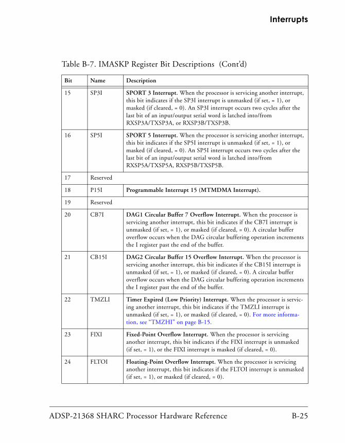
ADSP-21368 SHARC Processor Hardware Reference B-25
Interrupts
15 SP3I SPORT 3 Interrupt. When the processor is servicing another interrupt, this bit indicates if the SP3I interrupt is unmasked (if set, = 1), or masked (if cleared, = 0). An SP3I interrupt occurs two cycles after the last bit of an input/output serial word is latched into/from RXSP3A/TXSP3A, or RXSP3B/TXSP3B.
16 SP5I SPORT 5 Interrupt. When the processor is servicing another interrupt, this bit indicates if the SP5I interrupt is unmasked (if set, = 1), or masked (if cleared, = 0). An SP5I interrupt occurs two cycles after the last bit of an input/output serial word is latched into/from RXSP5A/TXSP5A, RXSP5B/TXSP5B.
17 Reserved
18 P15I Programmable Interrupt 15 (MTMDMA Interrupt).
19 Reserved
20 CB7I DAG1 Circular Buffer 7 Overflow Interrupt. When the processor is servicing another interrupt, this bit indicates if the CB7I interrupt is unmasked (if set, = 1), or masked (if cleared, = 0). A circular buffer overflow occurs when the DAG circular buffering operation increments the I register past the end of the buffer.
21 CB15I DAG2 Circular Buffer 15 Overflow Interrupt. When the processor is servicing another interrupt, this bit indicates if the CB15I interrupt is unmasked (if set, = 1), or masked (if cleared, = 0). A circular buffer overflow occurs when the DAG circular buffering operation increments the I register past the end of the buffer.
22 TMZLI Timer Expired (Low Priority) Interrupt. When the processor is servic-ing another interrupt, this bit indicates if the TMZLI interrupt is unmasked (if set, = 1), or masked (if cleared, = 0). For more informa-tion, see “TMZHI” on page B-15.
23 FIXI Fixed-Point Overflow Interrupt. When the processor is servicing another interrupt, this bit indicates if the FIXI interrupt is unmasked (if set, = 1), or the FIXI interrupt is masked (if cleared, = 0).
24 FLTOI Floating-Point Overflow Interrupt. When the processor is servicing another interrupt, this bit indicates if the FLTOI interrupt is unmasked (if set, = 1), or masked (if cleared, = 0).
Table B-7. IMASKP Register Bit Descriptions (Cont’d)
Bit Name Description

Interrupt Registers
B-26 ADSP-21368 SHARC Processor Hardware Reference
25 FLTUI Floating-Point Underflow Interrupt. When the processor is servicing another interrupt, this bit indicates if the FLTUI interrupt is unmasked (if set, = 1), or masked (if cleared, = 0).
26 FLTII Floating-Point Invalid Operation Interrupt. When the processor is ser-vicing another interrupt, this bit indicates if the FLTII interrupt is unmasked (if set, = 1), or masked (if cleared, = 0).
27 EMULI Emulator (Lower Priority) Interrupt. When the processor is servicing another interrupt, this bit indicates if the EMULI interrupt is unmasked (if set, = 1), or masked (if cleared, = 0). An EMULI occurs on reset and when an external device asserts the EMU pin. This interrupt has a lower priority than EMUI, but higher priority than software interrupts.
28 SFT0I User Software Interrupt 0. When the processor is servicing another interrupt, this bit indicates if the SFT0I interrupt is unmasked (if set, = 1), or masked (if cleared, = 0). An SFT0I occurs when a pro-gram sets (= 1) this bit.
29 SFT1I User Software Interrupt 1. When the processor is servicing another interrupt, this bit indicates if the SFT1I interrupt is unmasked (if set, = 1), or masked (if cleared, = 0).
30 SFT2I User Software Interrupt 2. When the processor is servicing another interrupt, this bit indicates if the SFT2I interrupt is unmasked (if set, = 1), or masked (if cleared, = 0).
31 SFT3I User Software Interrupt 3. When the processor is servicing another interrupt, this bit indicates if the SFT3I interrupt is unmasked (if set, = 1), or masked (if cleared, = 0).
Table B-7. IMASKP Register Bit Descriptions (Cont’d)
Bit Name Description

ADSP-21368 SHARC Processor Hardware Reference I-1
I INDEX
Numerics128-channel TDM, 5-416-bit to 32-bit word packing enable
(PACK), 5-6216-bit word lengths, 5-45, 6-32, 7-1432-bit word lengths, 5-45, 6-32, 7-148-bit word lengths, 6-31
Aaccessing IOP registers, latency in, 2-3accuracy, PWM, 8-17ACK (acknowledge) signal, 3-2, 3-19, 3-21acknowledge (ACK) pin, 3-20activate command, bank, 3-31active low frame sync select for frame sync
(INVFSx) bit, 13-12active low versus active high frame syncs,
5-39active state multichannel receive frame sync
select (LMFS) bit, 5-29AD1855 stereo DAC
power down, 6-7address
column, row and bank address mapping (32-bit), 3-53
core to external memory, 3-52decoding address bank, 3-53row in SDRAM, 3-34SDRAM (external memory space), 3-52SPORT IOP (listing), 5-50
address bus (ADDR) pin, 3-20, 3-83
addressing, 14-537-bit in TWI, 12-1, 12-15general call in TWI, 12-14IOP, 2-29pre-modify, 2-39restrictions on external memory, 3-3transfer phase in TWI, 12-6
AMISee also external port, SDRAM
controller, shared memoryADDR23-0 bits, 3-28control (AMICTLx) register, 3-25, A-17
to A-19DMA, 3-20hold cycles, 3-23idle cycle, 3-22memory bank support, 3-28modes, setting, 3-24most significant word first (MSWF) bit,
3-25packing data (PKDIS) bit, 3-25read/write throughput, 3-28reading external memory, 3-25receive (AMIRX) register, 3-25signals, 3-20status (AMISTAT) register, A-20unpacking data, 3-27wait states, 3-21writing external memory, 3-26

Index
I-2 ADSP-21368 SHARC Processor Hardware Reference
AMI bitsACK pin enable (ACKEN), A-18AMI enable (AMIEN), A-18buffer flush (FLSH), A-19bus hold cycle (HC), A-18bus idle cycle (HC), A-19disable packing (PKDIS), A-18external bus data width (BW), A-18most significant word first (MSWF),
A-18predictive read disable (NO_OPT), A-19read hold cycle (RHC), A-19wait state enable (WS), A-18
AND breakpoints (ANDBKP) bit, A-178AND, logical, 2-43, 14-3, A-178architecture
I/O processor, 2-25PWM, 8-2SPDIF transmitter, 9-8SPORT, 5-8TWI controller, 12-3
asynchronous access mode (external memory), 3-81
asynchronous memory interface. See AMIasynchronous serial communications
(UART), 11-2audience, intended, xxxiautobaud detection, 11-1
Bbandwidth in the I/O processor, 2-12bank
internal memory, 3-33SDRAM address mapping, 3-51 to 3-57
bank activate command, 3-31bank column address width, setting, 3-42baud rate, 6-30, 14-49
setting, 2-43, 6-10
baud rate (continued)SPIBAUD (serial peripheral interface
baud rate) register, 6-5, A-60UART, 11-4, 11-5, 11-12
beginning and ending an SPI transfer, 6-29BHD (buffer hang disable) bit, 5-64, 5-69BI (break interrupt) bit, 11-4bidirectional connections through the
signal routing unit, 4-13bidirectional functions (transmit, receive),
5-1biphase
encoded audio stream, 9-10encoded data register (SPDIF_RX_I),
9-18encoding, 9-11
bits See also peripheral specific bitscircular buffer x overflow interrupt
(CBxI), B-17, B-21, B-25emulator lower priority interrupt
(EMUI), B-14, B-18, B-19, B-21, B-23, B-26
timer expired high priority (TMZHI), B-15, B-19, B-23
timer expired low priority (TMZLI), B-17, B-21, B-25
block diagramI/O processor, 2-25input data port, 7-2PWM, 8-2SPDIF transmitter, 9-8SPORT, 5-8SRC, 10-9TWI controller, 12-3
boolean operatorAND, 2-43, 14-3, A-178OR, 7-30, 9-24, A-175, A-177, A-178
boot memory select (BMS) pin, 3-30, 14-39

ADSP-21368 SHARC Processor Hardware Reference I-3
Index
bootingboot kernel, 14-37BOOT_CFGx (boot source
configuration) pins, 14-38bootstrap loading, 14-37from SPI flash, 14-42SPI port, 14-42
broadcast mode, 6-3, 6-8buffer, 2-39, 5-7
chain pointer load sequence, 2-38circular, 2-37DAI pin, 4-3data buffer registers, 2-25data, addressing, 2-29external, 3-75external register, 3-45flash (AMI boot mode), 14-39output example, 4-12pin, defined, example, 4-10SPORT data, 5-1SPORT DMA, 5-15SPORT transmit and receive, 5-61SPORTs, activating, 5-4system example (multiple SDRAM),
3-46, 3-47UART restriction, 2-47
buffer hang disable (BHD) bit, 5-64, 5-69, A-39
burst length, in SDRAM, 3-32burst stop command (SDRAM), 3-32burst type definition, 3-32bus lock (BUSLK) bit, 3-88, 3-92bus lock and semaphores, 3-92bus master (Bm) condition, 3-82, 3-93bus master count (BCNT) register, 3-87bus master max time-out (BMAX) register,
3-87bus master, current (CRBMx) bit, 3-93,
A-9bus request BRx signal, 3-85
bus request, shared memory (BRx) pins, 3-81, 3-92
bus synchronized (BSYN) bit, 3-89, 3-93, A-9
bus transition cycle (BTC), 3-82buses
arbitration, 2-20, 3-79, 3-82bus lock, 3-92bus lock (BUSLK) bit, A-8bus master
timeout, 3-87conflict resolution ratio, 3-25contention, 2-20, 6-17, A-3errors in, 3-71external bus data width (BW) bit, A-18force sync of shared memory bus
(FSYNC) bit, A-8granting, 2-21, 6-20hold cycle bit, A-18I/O address (IOA), 2-29I/O data (IOD), 2-19, 2-20, 6-17I/O processor (IOP), 2-25, 5-44I2S and, 5-20idle cycle bit, A-19master, 3-84master timeout, 3-87serial, 5-27shared memory bus arbitration, 3-79slave, 3-84stalls on, 14-54synchronization, 3-88TDM method over serial, 5-27
bypass as a one-shot (strobe pulse), 13-13
Ccapacitors
bypass, 14-35decoupling, 14-35

Index
I-4 ADSP-21368 SHARC Processor Hardware Reference
CAS latencybit (SDCL), A-22definition, 3-32setting, 3-40
catastrophic interrupts, 4-65CBR (CAS before RAS) definition, 3-33CBxI (circular buffer x overflow interrupt)
bit, B-17, B-21, B-25center-aligned paired PWM
double-update mode, 8-11single-update mode, 8-9
chain loading sequence, 2-18chain pointer registers, 2-15, 2-16
defined, 2-27DMA buffer, 5-76SPI address in memory (CPSPI), 2-42,
6-16, 6-19SPORT address in memory (CPSPx),
A-51SPORTs, 5-77, 5-81, A-51starting address, 2-27
chained DMA, 2-14chaining, 2-13 to 2-42
chain insertion mode, 2-41chained DMA enable (SCHEN_A and
SCHEN_B) bit, 5-22, 5-63, 5-75, 5-81, A-38
chained DMA sequences, 2-14DMA, 2-13 to 2-42, 6-27in serial ports, 5-81, A-38SPI chained DMA enable (SPICHEN)
bit, 6-19chaining requests, multiple, 2-18changing SPI configuration, 6-21channel
buffer, 2-7DMA, 2-9, 2-12, 2-13interrupt, 2-8priority scheme, 2-2status, 2-7, 2-13
channel B transmit status register (SPDIF_TX_CHSTB), A-90, A-91
channel double frequencey mode, single, 9-8
channel mode (SPDIF), two, 9-8channel number, encoded, 7-19channel selection registers, 5-31channels, input data port, 7-1circular, 2-39circular buffering, 2-37, 2-39CLKOUT (clock output) signal, 14-12clock A source (CLKASOURCE) bit,
A-157clock divisor (CLKDIV) bits, A-44clock input (CLKIN) pin, 4-72, 13-2,
13-20, 14-20clock rising edge select (CKRE) bit, 5-62clocks and system clocking
CLKOUT and CCLK clock generation, 14-30
clock and frame sync frequencies (DIVx) registers, 5-69, A-44
clock distribution, 14-34clock divisor (CLKDIV) bit, A-44clock input (CLKIN) pin, 14-13, 14-20clock output enable, 13-3clock polarity (CLKPL) bit, A-55clock ratio, 14-31clock relationships, 14-31clock rising edge select (CKRE) bit, 5-62,
A-38clock signal options, 5-71clocking edge selection, 7-12core clock ratio, 14-31definitions, 14-31determining switching frequencies,
14-29external master clock, 14-21frame sync bypass mode, 13-6

ADSP-21368 SHARC Processor Hardware Reference I-5
Index
clocks and system clocking (continued)frame sync bypass mode, direct bypass,
13-6frame sync bypass mode, one shot, 13-6internal clock select (ICLK) bit, A-37jitter, 14-33master clock (MCLK), 10-8, 13-18output control (ENCLKA/B) bits, 13-3precision clock generator registers, 13-3,
13-7SDRAM controller, 3-37serial port count (SPCNTx) registers,
A-45source select (MSTR) bit, A-37SPI clock phase select (CPHASE) bit,
A-55SPI clock rate, 6-5
code select (CSEL) bit, 3-82column, row and bank address mapping
(32-bit), 3-53commands
auto-refresh, 3-70bank activate, 3-31, 3-65booting, 14-48, 14-51burst stop, 3-32load mode register, 3-64NOP, 3-72precharge, 3-34, 3-66read/write, 3-67, 14-50SDRAM read, A-22self-refresh, 3-70SPI master, 6-20SPI transfer, 6-10
compand data in place, 5-48companding (compressing/expanding), 5-3conditioning input signals, 14-32configurable channels, digital audio
interface interrupts, A-112configuring frame sync signals, 5-6connecting peripherals, 4-8
connectionsgroup A, DAI, clock signals, 4-19group A, DPI, input routing signals,
4-52group B, DAI data signals, 4-25group B, DPI, pin assignment signals,
4-56group C, DAI, frame sync signals, 4-31group C, DPI, pin enable signals, 4-64group D, DAI, pin signal assignments,
4-36group E, DAI, miscellaneous signals,
4-43group F, DAI, pin enable signals, 4-47
controller, SDRAM, 3-30conventions, manual, xliiicore access to IOP registers, 2-3core address mapping, 3-52core clock cycle, 6-30core PLL, 13-2core transmit/receive operations, 6-13count registers
DMA sport (CSPx), A-51DMA, defined, 2-27DMA, restrictions, 2-31IDP DMA (IDP_DMA_Cx), 7-28
CPSPI (SPI chain pointer) registers, A-65crossover mode, PWM, 8-16crosstalk, reducing, 14-34CSPI, CSPIB (SPI DMA word count)
registers, A-64CSPx (peripheral DMA counter) registers,
2-31, A-51customer support, xxxv
DDAI
buffers, pin, 4-3channel number, encoded, 7-19

Index
I-6 ADSP-21368 SHARC Processor Hardware Reference
DAI (continued)clock routing control registers (group A),
4-19configurable interrupts, A-112configuration macro, 4-77connecting peripherals with, 4-8default configuration, 4-18general-purpose (GPIO) and flags, 4-64interrupt controller, 4-65 to 4-71interrupt controller registers, A-112interrupts, 4-66, 7-22, A-112latches, high and low priority, 4-69miscellaneous signals, 4-65pin buffer example, 4-3, 4-10, 4-12pin buffer, bidirectional, 4-13rising and falling edge masks, 4-70selection group B (data), 4-25selection group C (frame sync), 4-31selection group D (pin assignments),
4-36selection group E (miscellaneous signals),
4-43 to 4-46selection group F, 4-47SRU1 connections for SPORTx, 4-14,
4-16system configuration, sample, 4-76system design, 4-3
DAI registerscore interrupt priority assignment
(DAI_IRPTL_PRI), 4-69core interrupt priority assignment
register (DAI_IRPTL_PRI), 7-19, A-114
DAI_IRPTL_FE registeras replacement to IMASK, 4-69
DAI_IRPTL_H register as replacement to IRPTL, 4-69
DAI_IRPTL_L register as replacement to IRPTL, 4-69
DAI registers (continued)DAI_IRPTL_RE register as replacement
to IMASK register, 4-69falling edge interrupt mask register
(DAI_IRPTL_FE), A-115high priority interrupt
(DAI_IRPTL_H), A-113high priority interrupt latch register
(DAI_IRPTL_H), 7-17, 7-28, A-114interrupt falling edge (DAI_IRPTL_FE),
7-19, A-113interrupt high priority
(DAI_IRPTL_H), A-114interrupt rising edge (DAI_IRPTL_RE),
7-19, A-113low priority interrupt (DAI_IRPTL_L),
A-113low priority interrupt latch register
(DAI_IRPTL_L), 7-17, A-114pin status (DAI_PIN_STAT), A-112,
A-116ping-pong DMA status
(SRU_PINGx_STAT), A-110resistor pull up enable
(DAI_PIN_PULLUP), A-111, A-115resistor pullup enable
(DAI_PIN_PULLUP), A-111, A-115rising edge interrupt mask register
(DAI_IRPTL_RE), A-115shadow high priority interrupt latch
register (DAI_IRPTL_HS), A-114shadow low priority interrupt latch
register (DAI_IRPTL_LS), A-114status (DAI_STAT), 7-19, 7-25, 7-26,
A-109data
alignment, external port, 3-25buffers in DMA registers, 2-32direction control (SPTRAN) bit, 5-64,
A-39

ADSP-21368 SHARC Processor Hardware Reference I-7
Index
data (continued)packing and unpacking, 5-45
data buffers, in serial ports, 5-4data bus (DATA) pins, 3-20data direction control (SPTRAN) bit, 5-64,
A-39data fetch, external port, 3-25data memory breakpoint hit (STATDx)
bit, A-181data pin multiplexing, A-8data pins, function of, 14-7data ready (DR) status flag (UART), 11-5data status (DXS_A, DSX_B) bits, 5-66data type, 5-46
formatting (multichannel), 5-46formatting (non-multichannel), 5-46select (DTYPE) bit, 5-61, A-37
data wordsin FIFO, 7-15packing, 5-45, 14-42single word transfers, 5-81transferring, 2-49, 5-4, 5-17, 5-22, 5-31,
5-37, 6-33UART, 11-4
data-independent frame sync, 5-41(DIFS) mode, 5-41
dead time equation, 8-8definition
burst type, SDRAM, 3-32CAS latency, SDRAM, 3-32CBR, SDRAM, 3-33
delay line DMA, 2-40diagrams
uniprocessor system with multiple SDRAM devices diagram, 3-46, 3-47
DIFS (data independent frame sync select) bit, A-38
digital audio interface. See DAIDIVEN (PLL divider enable) bit, A-170,
A-172
division multiplexed (TDM) mode, time, 9-19
divisorclock output, 13-3reset, UART, 11-12SPORT (DIVx) registers, 5-6, A-44
divisor, UART, 11-11, A-125DIVx (divisor) registers, 5-6, 5-69, A-44DLAB (divisor latch access) bit, 11-6, 11-7,
A-119, A-122, A-123DMA
See also I/O processor, external port, SPI, SPORTs
active chain TCB, 2-41and UART, 2-44chain insertion mode, 2-41chain insertion, active chain, 2-41chaining in SPI, 2-42channel buffer registers, listed, 2-32channel parameter registers, 2-32channel priority, 2-19complete interrupt, 2-8configuring in the I/O processor, 2-2control registers, 2-32controller enhancements, 1-11count registers, A-73data buffer registers, 2-25delay line, 2-40enable bits, 2-48enabling, 2-48error interrupts, 6-25external port throughput, 3-18IDP index registers, A-70IDP modify registers, A-71index registers, 2-29, A-72input data port enable (IDP_DMA_EN)
bit, 7-20interrupt regeneration, 2-11interrupt-driven, 2-8latency, 2-13

Index
I-8 ADSP-21368 SHARC Processor Hardware Reference
DMA (continued)master mode operation, 6-15memory-to-memory, 2-48multiple chain requests, 2-18non-chained, 2-13parameter registers, 2-17ping-pong, 7-22 to 7-24ping-pong enable (IDP_PING) bits,
A-68sequence start, end, 2-14sequences, TCB loading, 2-16slave mode operation, 6-19SPI chain pointer registers, A-65SPI count registers, A-64SPI modifier registers, A-64SPI slave mode, 6-11, 6-12SPORT chain status bits (DMACHSxy),
A-43SPORT index registers, A-50SPORT modify registers, A-50SPORT status bit (DMASxy), A-43switching from receive to transmit mode,
6-24switching from transmit to receive mode,
6-23transfers in IDP, 7-20transmit or receive operations (SPI), 6-16UART, 11-7
DMA enable bits (all peripherals), 2-48DMA registers
channel listed, 2-32DMACx (external port DMA registers),
A-14Dolby, DTS audio standards, 9-16double frequencey mode, single channel,
9-8DPI
connections, group A, 4-52 to 4-56connections, group B, 4-56 to 4-60connections, group C, 4-60 to 4-64
DPI (continued)default configuration, 4-51input routing (group A) signals, 4-52interrupts, 4-67pin assignment (group B) signals, 4-56pin enable (group C) signals, 4-60registers, A-109
DSP serial mode, 5-74DSxEN (SPI device select) bits, 6-15, A-58DTYPE (data type) bits, 5-61, A-37
DSP serial mode data formatting, 5-46multichannel data formatting, 5-46
duty cycles and dead time in PWM, 8-8DXS_A (data buffer channel B status) bit,
A-40DXS_B, DSX_A (data buffer channel A/B
status) bit, 5-66, A-39, A-40
Eearly vs. late frame syncs, 5-40edge-related interrupts
four conditions, 4-70EEMUINENS bit, A-182EEMUINFULLS bit, A-182EEMUOUIRQENS bit, A-181EEMUOUTRDY bit, A-181EEMUSTAT register, A-179EIPPx (DMA external index) registers,
2-27ELSI (enable RX status interrupt) bit, 11-9,
A-123EMPPx (DMA external modify) registers,
2-28EMUI (emulator lower priority interrupt)
bit, B-14, B-18, B-19, B-21, B-23, B-26
emulatorinterrupt (EMUI) bit, B-14, B-18, B-19,
B-21, B-23, B-26

ADSP-21368 SHARC Processor Hardware Reference I-9
Index
enablebreakpoint (ENBx) bit, A-178clock outputs, 13-3DMA, 7-20DMA interrupt (INTEN) bit, 6-34external port (asynchronous memory
interface), A-18input data port, 7-15multichannel mode in SPORTs, A-42PCGs, 13-7PDAP, 7-12pulse width modulation groups, 8-4sample rate converters, 10-22SPDIF transmit buffer, 9-25SPI DMA, 6-16SPI slave, 6-20SPORT DMA (SDEN bit), 5-24SPORT master mode (MSTR), 5-18
enable receive buffer full interrupt (ERBFI) bit, 11-7, A-123
enable transmit buffer empty interrupt (ETBEI) bit, 11-7, A-123
endian format, 5-15, 5-45, 5-62, 6-1, A-37enhanced emulation
feature enable (EEMUENS) bit, A-182FIFO status (EEMUOUTFULLS) bit,
A-182INDATA FIFO status
(EEMUINFULLS) bit, A-182OUTDATA FIFO status
(EEMUOUTFULLS) bit, A-182OUTDATA interrupt enable
(EEMUOUIRQENS) bit, A-181OUTDATA ready (EEMUOUTRDY)
bit, A-181equation
clock, 14-30dead time, 8-8duty cycles in PWM, 8-10frame sync frequency, 5-71
equation (continued)PWM dead time, 8-8PWM switching frequency, 8-5SDRAM refresh rate, 3-50serial clock frequency, 5-70serial port clock divisor, 5-70SPI clock baud rate, A-60TWI clock divider, 12-5
error signals and flags, 6-35errors
clearing in SPI, 6-23, 6-25conditions in DAI/DPI, 4-71data buffer status (SPORT), 5-65data in SPORTs, 5-42data truncation, 1-4frame sync (SPORT), 5-26, 5-42IDP FIFO, 7-15internal bus (SDRAM), 3-71PCG quantization, 13-2preventing in DMA chaining, 2-16reception (SPI), 6-37S/PDIF error handling, 9-1, 9-22 to 9-23S/PDIF receiver, 9-17SDRAM, 3-77SPI DMA, 6-14, 6-19SPI master, 6-6SPI mode fault, 6-36SPI transmission, 6-21, 6-37SPORT, 5-15SRC, 10-3SRC phase difference, 10-12SRC resampling, 10-4TWI master mode, 12-17, 12-18TWI repeat start, 12-19TWI slave transfer, 12-14, 12-16UART, 11-4, 11-9UART baud rate, 11-12UART DMA, 2-46, 11-7UART line, 11-7UART sampling, 11-6
Index
I-10 ADSP-21368 SHARC Processor Hardware Reference
errors/flags, DMA, external port, host port, serial port, SPI port, UART port, 6-35
examplesbidirectional DAI pin buffer, 4-13DAI pin buffer, 4-10DAI pin buffer output, 4-12hold time in AMI, 3-24idle cycle in AMI, 3-23interrupt latency, regeneration, 2-11PCG setup for I2S or left-justified DAI,
13-15pin buffer, 4-10PLL, 14-16programming SPORTs (DMA
chaining), 5-83programming SPORTs direct core
access, 5-86programming SPORTs transmit
(DMA), 5-89programming the IDP, 7-31 to 7-33programming the PCG channels, 13-23
to 13-25rotating priority arbitration, 3-86SPI DMA chaining, 2-43SRU1 connections for SPORTx, 4-14,
4-16examples, timing
IDP hold timing mode 00, 7-13IDP hold timing mode 01, 7-14IDP I2S, 7-7IDP left-justified sample pair, 7-7PDAP, 7-14SPI clock, 6-5SPI transfer protocol, 6-28, 6-29SPORT framed vs. unframed data, 5-40SPORT left-justified sample pair mode,
5-19SPORT normal vs. alternate framing,
5-40SPORT word select, 5-25
execution stalls, bus transition, 3-84external data path width, setting, 3-43external master clock, 14-21external memory
access timing, 3-36address bank decoding, 3-53banked, 3-30banks, 3-30external physical address, 3-29interface, 3-20most significant word first (MSWF) bit,
A-18packing and unpacking (PKDIS) bits,
A-18pin descriptions, 3-19signals, 3-16, 3-20
external memory DMAchained, setting up, 2-36DMA count (ECEPx) registers, 2-28DMA index (EIPPx) registers, 2-27DMA modifier (EMEPx) registers, 2-28
external memory restrictions, 3-52external port
buffer regsiter pipeline option, 3-45bus hold cycle bit, A-18bus idle cycle bit, A-19chain pointer loading sequence, 2-38,
2-40chain pointer register (CPEP), 2-36channel freezing, 3-18conflict resolution, 3-25core address mapping, 3-52data pin mode select (EPDATA) bits,
A-8delay line DMA, 2-40DMA, 2-35 to 2-40DMA registers, A-14 to A-16DMA throughput, 3-18hold cycles, 3-23modes, 3-24

ADSP-21368 SHARC Processor Hardware Reference I-11
Index
external port (continued)modes, setting, 3-24read hold cycle (RHC) bits, A-19
external port bitsbank select (BxSD), A-11bus priority (EPBR), A-12data enable (DATA), A-13delay line write pointer write back status
(WBS), A-16DMA chain status (CHS), A-16DMA chaining enable (CHEN), A-15DMA channel priority, A-12DMA circular buffer enable (CBEN),
A-15DMA delay-line enable (DLEN), A-15DMA direction (DMADR), A-15DMA enable (DMAEN), A-15DMA external interface status (EXTS),
A-16DMA FIFO status (DFS), A-15DMA flush FIFO (DFLSH), A-15DMA transfer direction status (DIRS),
A-16DMA transfer status (DMAS), A-15flush tap list FIFO (TFLSH), A-15freeze length (FRZDMA), A-12freeze length core (FRZCR), A-12tap list FIFO status (TFS), A-15tap list loading status (TLS), A-16
external port control bus, 3-25, 3-26external port DMA
chain pointer loading sequence, 2-37chained, 2-36channel priority, 2-35delay line, 2-39FIFO, 2-35set up, 2-36
external port registers, A-10 to A-26AMI control (AMICTLx), A-17DMA control (DMACx), 2-26
external port registers (continued)length and base (ELEP, EBEP), 2-37
FFE (framing error) bit, 11-4FIFO
control and status in input data port, 7-15
overflow clear bit, 7-15to memory data transfer, 7-16
FIR filter in SRC, 10-2, 10-7fixed-point overflow interrupt (FIXI) bit,
B-17, B-21, B-25flag select bits (SPI), 6-10flags
digital audio interface, 4-64errors DMA, external port, host port,
serial port, SPI port, and UART port, 6-35
flag interrupt mode (IRQxEN) bits, A-7input/output (FLAGx) pins, 6-4, 14-8
FLAGx pins, 6-4, 14-8floating-point
compatibility, 1-3FLTII (invalid operation interrupt) bit,
B-17, B-21, B-26FLTOI (overflow interrupt) bit, B-17,
B-21, B-25FLTUI (underflow interrupt) bit, B-17,
B-21, B-26overflow interrupt (FLTOI) bit, B-17,
B-21, B-25underflow interrupt (FLTUI) bit, B-17,
B-21, B-26FLTII (floating-point invalid operation
interrupt) bit, B-21, B-26formula, for frame sync pulse, 5-70frame sync
A source (FSASOURCE) bit, A-157active low vs. active high, 5-39

Index
I-12 ADSP-21368 SHARC Processor Hardware Reference
frame sync (continued)both enable (FS_BOTH) bit, 5-64early vs. late, 5-40equations, 13-11frequencies, 5-69in multichannel mode, 5-28internal vs. external, 5-38options (FS_BOTH and DIFS), 5-18,
5-24options (FS_BOTH), 5-18output, synchronizing, 13-7PCG B source (FSBSOURCE) bit,
13-13signals, configuring, 5-6SPORT frame on rising frame sync
(FRFS) bit, 5-17SPORT frame sync required (FSR) bit,
5-63frame sync rates
setting in SPORTs, 5-17, 5-21setting the internal serial clock in
SPORTs, 5-21framed versus unframed data in SPORTs,
5-37framing bits, SPORT, 5-17freezing, channel (in external port DMA),
3-18frequencey mode, single-channel,
double-frequency, 9-8frequency of the frame sync output, 13-9full-duplex operation, specifications, 5-6
Ggeneral-purpose (GPIO) and flags for
digital audio interface, 4-64general-purpose IOP timer 2 interrupt
mask (GPTMR2IMSK) bit, B-10general-purpose IOP timer interrupt mask
(GPTMRxIMSK) bits, B-10generators, optional reset, 14-27
glitch vulnerability (SPORTs), 5-10GM (get more data) bit, 6-11, 6-20, 6-37,
A-54ground plane, in PCB design, 14-34groupings of signals in DAI/DPI, 4-8
Hhandshaking, external port, 3-20, 3-79hardware interrupt
bits, B-15, B-16, B-19, B-20, B-24signals IRQ2-0, 14-4, 14-6, 14-8, B-16,
B-24high and low priority latches, 2-7, 4-69hold cycle (external bus) bit, A-18hold cycles, external port, 3-23hold off, processor bus transition, 3-84hold time
inputs, 14-32recognition of asynchronous input,
14-32hold time cycles, setting, 3-23hysteresis on RESET pin, 14-33
II/O address breakpoint hit (STATI0) bit,
A-181I/O interface to peripheral devices, 5-1I/O processor
See also DMA; specific peripheralsaddress bus (IOA), 2-29addressing in, 2-29bandwidth, 2-12baud rate, 2-43bus arbitration and contention, 2-20bus diagram, 2-25bus grant, 2-21chain insertion mode (DMA), 2-41chain pointer (CPSPI) register, 2-16chain pointer registers, 2-27, 2-43

ADSP-21368 SHARC Processor Hardware Reference I-13
Index
I/O processor (continued)chained DMA, 2-14configuring DMA, 2-2count registers, 2-27, 2-31DAI interrupt registers (DAI_IRPTL_H,
DAI_IRPTL_L), 2-7data (IOD) bus, 2-20data buffers in DMA, 2-32DMA channel priority, 2-19DMA channel registers, 2-32DMA enable (DEN) bit, 2-48DMA interrupt registers, 2-7DMA interrupt vector locations, 2-8DMA parameter registers, 2-17DMA sequence complete interrupt, 2-8external count (ECEPx) registers, 2-28external index (EIPPx) registers, 2-27external modify (EMEPx) registers, 2-28interrupt driven I/O, 2-6interrupt service routine restriction, 2-5latency, 2-11 to 2-13memory access, DMA, 2-8polling driven I/O, 2-12program control interrupt (PCI) bit, 2-8regenerated interrupts, avoiding, 2-11registers, listed, A-2restrictions, 2-2, 2-31restrictions (ISR), 2-5stall conditions, 2-3stall cycles in, 2-5status driven I/O, 2-12status polling, 2-12transfer types, 2-1type 1 or LW instructions, 2-2
I2C port. See TWI controllerI2S
(Tx/Rx on left channel first), 5-11, 5-12, A-30
(Tx/Rx on right channel first), 5-11, 5-12, A-30
I2S (continued)control bits, 5-21example for DAI, 13-15mode, 5-74mode (IDP), 7-3, 7-5, 7-21SPCTLx control bits, 5-22timing (IDP), 7-7transmit and receive channel order
(FRFS), 5-18, 5-23ICLK (internal clock select) bit, A-37identification (ID2-0) pin, 3-81identification code (IDC) bit, 3-93, A-10idle cycle (external bus) bit, A-19idle cycle in external port, 3-22IDP
(DAI) interrupt service routinesteps, 7-28
clocking select, 7-12FIFO control, 7-15FIFO memory data transfer, 7-16FIFO status, 7-15hold input, 7-12illustrated, 7-1interrupt-driven transfers, 7-17, 7-18interrupts, 7-17, 7-19, 7-22, 7-24masking, 7-9, A-74memory data transfer, 7-16packing modes, 7-9, 7-11packing unit, 7-9parallel input mode, 7-8PDAP control (IDP_PP_CTL) register,
7-9ping-pong DMA, 7-22 to 7-24programming examples, 7-31serial inputs, 7-3serial modes, setting, 7-5
IDP bitsbus hang disable (IDP_BHD), 7-15,
7-19, A-67

Index
I-14 ADSP-21368 SHARC Processor Hardware Reference
IDP bits (continued)clear buffer overflow (IDP_CLROVR),
7-15, 7-16, 7-25, A-67DMA enable (IDP_DMA_EN), 7-20,
7-22, 7-25, A-67DMA status (IDP_DMAx_STAT),
7-26, A-111enable (IDP_ENABLE), 7-15, 7-18,
7-20, 7-22, 7-23, A-67FIFO number of samples
(IDP_FIFOSZ), 7-15, 7-16, 7-19, A-111
FIFO overflow (IDP_FIFO_OVER), 7-15, 7-16
FIFO overflow (SRU_OVF), 7-25FIFO samples exceed interrupt
(IDP_FIFO_GTN_INT), 7-17, 7-19, A-113
frame sync format (IDP_SMODEx), 7-4, 7-18, 7-21, A-67, A-70
IDP_DMA_EN (DMA enable restriction), 7-19
IDP_DMA_EN (input data port DMA enable), 7-20
monitor number of samples (IDP_NSET), 7-17, 7-18, 7-19, A-67
PDAP clock edge (IDP_PDAP_CLKEDGE), 7-12, 7-18, 7-21, A-77
PDAP enable (IDP_PDAP_EN), 7-12, 7-22, A-78
PDAP input mask bits, 7-18PDAP mask (IDP_Pxx_PPMASK), 7-9,
7-21, A-74PDAP packing mode
(IDP_PDAP_PACKING), 7-9, A-77PDAP reset (IDP_PDAP_RESET), 7-8,
A-78ping-pong DMA enable (IDP_PING)
bits, A-68
IDP bits (continued)port select (IDP_PORT_SELECT), 7-8,
7-18, 7-21, A-77reset (IDP_PDAP_RESET) bit, A-78
IDP registerscontrol (IDP_CTL0), 7-18, 7-19, 7-20,
A-66control (IDP_CTL1), 7-19, A-68DMA control, 2-26, A-70DMA count (IDP_DMA_Cx), 7-21,
7-28, A-71DMA index (IDP_DMA_Ix), 7-21,
7-28, A-70DMA modify (IDP_DMA_Mx), 7-21,
7-28, A-71FIFO (IDP_FIFO), 7-15, 7-16, 7-17,
A-69IDP_CTLx (input data port control),
7-18, 7-19, 7-20, A-66, A-68IDP_DMA_AIx (ping-pong DMA
index), 7-23IDP_DMA_PCx (ping-pong DMA
count), 7-23PDAP control (IDP_PP_CTL), 7-8, 7-9,
7-12, A-74ping-pong DMA count
(IDP_DMA_PCx) registers, 7-23ping-pong DMA index
(IDP_DMA_AIx), 7-23IFS (SPORT internal frame sync select) bit,
5-63, A-38IICD (illegal input condition interrupt) bit,
B-15, B-19, B-23IISPI (SPI DMA start address) register,
A-64IISPx (serial port DMA internal index)
registers, 2-27, 2-29, A-50illegal input condition detected (IICD) bit,
B-15, B-19, B-23IMASK (interrupt mask) register, B-18

ADSP-21368 SHARC Processor Hardware Reference I-15
Index
IMASKP (interrupt mask pointer) register, B-22
IMSPI (serial peripheral interface address modify) register, 6-16, 6-19, A-64
IMSPx (SPORT DMA address modifier) registers, 2-27, 2-29, A-50
INCLUDE directory, 5-49INDATA interrupt enable
(EEMUINENS) bit, A-182INDIV (input divisor) bit, A-172input data port. See IDPinput setup and hold time, 14-32input signal conditioning, 14-32input slave select enable (ISSEN) bit, 6-36,
A-54input synchronization delay, 14-8instruction address breakpoint hit
(STATIx) bit, A-181instruction rate, 14-14instructions
atomic, using for clock and frame sync, 13-10
conditional in SDRAM, 3-82, 3-93dual data move restriction, 3-78external memory fetch, 3-25packed, 3-20return from interrupt, 4-67
INTEN (DMA interrupt enable) bit, 6-34interconnections, master-slave, 6-4internal clock select (ICLK) bit, 5-62internal frame sync (SPORT IFS) bit, 5-63internal I/O bus, 2-19internal I/O bus arbitration (request and
grant), 2-19internal interrupt vector table (IIVT) bit,
A-6internal memory
DMA count (CSPx) registers, A-51DMA index (IDP_DMA_Ix) registers,
7-28
internal memory (continued)DMA index (IISPx) registers, 2-27, 2-29,
A-50DMA modifier (IDP_DMA_Mx)
registers, 7-28DMA modifier (IMSPx) registers, 2-27,
2-29memory-to-memory data transfers, 2-48transfers, 2-48
internal memory banks, 3-33internal serial clock
(ICLK) bit, 5-62setting, 5-17
internal transmit frame sync (IFS) bit, 5-63internal vs. external frame syncs, 5-38INTERR (enable interrupt on error) bit,
6-34interrupt
hardware, B-15, B-20input x interrupt (IRQxI) bit, B-15,
B-16, B-20, B-24latch (IRPTL) register, B-13latch/mask (LIRPTL) register, B-6mask (IMASK) register, B-18mask pointer (IMASKP) register, B-22peripheral interrupt priority registers
(PICR), A-164PWM interrupt (P13I) bit, B-9transfers, starting, 7-18, 7-20, 7-23
interrupt and timer pins, 14-8interrupt controller, digital audio interface,
4-65, A-112interrupt driven DMA, I/O processor, 2-8interrupt input (IRQ2-0) pins, 14-8interrupt input x interrupt (IRQxI) bit,
B-19, B-24interrupt latch (IRPTL) register, 6-34,
B-13interrupt latch/mask (LIRPTL) registers,
6-34, B-6

Index
I-16 ADSP-21368 SHARC Processor Hardware Reference
interrupt mask (IMASK) control register, B-18
interrupt vector, sharing, 5-72interrupts, B-15, B-19, B-24
(enable RX status interrupt) bit, A-123assigning priority for UART, 11-11catastrophic, 4-65conditions for generating interrupts in
SPORTs, 5-75conditions, UART, 11-9digital audio interface, 4-66, 7-22digital peripheral interface, 4-67I/O processor, using in the, 2-6latch status for, B-13listed in registers, B-1non-maskable software (RSTI), A-6normal, 4-65UARTLSIE (enable UART RX status
interrupt) bit, 11-9INVFSx (active low frame sync select for
frame sync) bits, 13-12IOP register set, 5-49IRPTL (interrupt latch) register, B-13IRQ2-0 (hardware interrupt) pins, 14-8IRQxI (hardware interrupt) bit, B-15,
B-16, B-19, B-20, B-24ISSS (input service select) bit, A-58
Jjitter, clock, 14-33JTAG interface pins, 14-12
LLAFS (late transmit frame sync select) bit,
A-38LAFS (SPORT late transmit frame sync
select) bit, 5-11, 5-14, 5-16, 5-20, 5-21, 5-40, 5-63, A-30, A-38
latchinghigh and low priority (DAI/DPI), 4-69interrupt latch (IRPTL) register, B-13status for interrupts, B-13
latchup, 14-32latency
CAS, setting, 3-40definition, CAS, 3-32I/O processor registers, A-2in SPORT registers, 5-58input synchronization, 14-8instruction fetch, external memory, 3-25setting CAS, 3-40
left-justified data (S/PDIF), 9-7, 9-10left-justified data (SRC), 10-13
framing, 10-17matched-phase mode, 10-17setting, 10-14
left-justified sample pair mode (IDP), 7-21data transfer, core, 7-18data transfer, DMA, 7-21DMA, 7-26FIFO data packing, 7-6setting, 7-5timing, 7-7
left-justified sample pair mode (SPORTs), 5-10, 5-16, 5-17
control bits, 5-17Tx/Rx on FS falling edge, 5-12, A-30Tx/Rx on FS rising edge, 5-12, A-30
left-justified waveform (PWM), 8-1LIRPTL (interrupt) registers, 6-34, B-6little endian (TWI controller), 12-9loader kernel, 14-37low active transmit frame sync (LFS, LTFS
and LTDV) bits, 5-63, A-159LRFS (SPORT logic level) bit, 5-29LSBF (least significant bit first) bit, 5-62,
A-37

ADSP-21368 SHARC Processor Hardware Reference I-17
Index
Mmaking connections via the signal routing
unit, 4-15manual
contents, xxxiiconventions, xliiinew in this edition, xxxivrelated documents, xxxviiirevisions, xxxiv
maskable interrupts, A-6masking data (SDRAM), 3-33master clock, external, 14-21master input slave output (MISOx) pins,
6-2, 6-7, 6-8, 6-27master mode enable (SPORT), 5-13, 5-29master mode operation, SPI, 6-10master out slave in (MOSIx) pin, 6-2, 6-7,
6-27master-slave interconnections, 6-4memory
boot memory, 3-30, 14-39data transfer, FIFO, 7-16internal banks, 3-33
memory banks, internal, 3-33memory read RD pin, 3-21, 3-83memory select (flags) programming
(MSEN) bit, A-8memory select (MSx) pins, 3-21, 3-53,
3-83, 3-84, 3-89memory transfer types, 2-1memory-mapped emulation, breakpoint
registers, 2-4memory-mapped IOP RXSPI buffer
registers, A-59memory-to-memory DMA, 2-48memory-to-memory DMA register, A-28MISCAx_I (signal routing unit external
miscellaneous) register, 13-13miscellaneous signals, 4-65MISOx pins, 6-27
modebroadcast (SPI), 6-8chain insertion, 2-14, 2-41chained DMA, 2-41left-justified (SPORT), 5-16left-justified sample pair (IDP), 7-3loopback (SPORT), 5-6, A-42master (SPI), 6-38multichannel (SPORT), 5-3open drain (SPI), 6-9packing (IDP), 7-9, 7-10right-justified (IDP), 7-3self-refresh, 3-34serial mode settings (IDP), 7-4single channel double frequency
(S/PDIF), 9-8standard serial (SPORT), 5-12standard serial, signals (SPORT), 5-5TDM (SPORT), 5-26time division multiplexed (TDM), 9-19two channel (SPDIF), 9-8UART DMA, 2-44UART non-DMA, 11-13
mode (SPDIF), two channel, 9-8mode fault (multimaster error) SPI DMA
status (MME) bit, 6-35, 6-36mode fault error (MME) bit, 6-9, 6-35,
6-36mode register (SDRAM controller), 3-33MOSIx pins, 6-27MSBF (most significant byte first) bit, A-54MSx pins, memory select, 3-52, 3-53MTM_FLUSH (memory-to-memory
FIFO flush) bit, 2-48MTMDMACTL (memory-to-memory
DMA control) register, 2-48MTxCCSx (serial port transmit compand)
registers, A-47MTxCCSy and MRxCCSy (multichannel
compand select) registers, 5-47

Index
I-18 ADSP-21368 SHARC Processor Hardware Reference
MTxCSx (serial port transmit select) registers, A-46
multichannel A and B channels, A-30multichannel compand select (MTxCCSy
and MRxCCSy) registers, 5-47multichannel operation (SPORT), 5-25multichannel selection registers (SPORT),
5-31multichannel, A and B channels, 5-12multi-device SPI configuration, 6-12multimaster conditions, 6-12multimaster environment, 6-8multiplexed (TDM) mode, time division,
9-19multiplexing
in external port data pins, A-8pins, 14-3 to 14-12PWM pins, A-8
multiprocessing. See shared memory
Nnegate breakpoint (NEGx) bit, A-175,
A-177NINT (pending interrupt) bit, 11-10non-chained DMA, 2-13normal frame sync (SPORT), 5-40normal interrupts, 4-65
OOE (overrun error) bit, 11-4one shot frame sync A or B (STROBEx)
bits, 13-12one shot option (STROBEB) bit, 13-13one shot, defined, 13-13OPD (open drain output) pin, 6-9OPMODE (SPORT serial port operation
mode) bit, 5-13, 5-17OR, logical, 7-30, 9-24, A-175, A-177,
A-178
OSPID (operating system process ID), 2-4, A-182
OSPIDENS (operating system process ID) register enable bit, A-182
output control unit, PWM, 8-17output pulse width, defined, 13-13output strobe, PDAP, 7-14over-modulation, PWM, 8-12
PPACK (SPORT packing enable) bit, A-37packing modes in PDAP, illustrated, 7-10packing, data, 6-32page size (SDRAM), A-25page sizes in SDRAM, 3-34parallel data acquisition port. See PDAP,
IDPparallel input mode, 7-8parameter registers, I/O processor, 2-25PCG
active low frame sync select for frame sync (INVFSx) bits, 13-12
bypass mode, 13-12clock A source (CLKASOURCE) bit,
A-157clock input (CLKIN) pin, 4-72, 13-2,
13-20clock input source enable
(CLKx_SOURCE_IOP) bit, A-161clock with external frame sync enable
(FSx_SYNC) bit, A-161control (PCG_CTL_Ax) registers,
13-13, A-156division ratios, 13-16enable clock (ENCLKx) bit, A-156enable frame sync (ENFSx) bit, A-156frame sync A source (FSASOURCE) bit,
13-13, A-157frame sync B source (FSBSOURCE) bit,
13-13, A-157

ADSP-21368 SHARC Processor Hardware Reference I-19
Index
PCG (continued)frame sync input source enable
(CLKx_SOURCE_IOP) bit, A-161frame sync with external frame sync
enable (FSx_SYNC) bit, A-161, A-162
frame syncs, 13-11frequency of the frame sync output, 13-9one shot frame sync A or B (STROBEx)
bits, 13-12one shot option, 13-13PCG_CTLA0 (control) register, A-156phase shift of frame sync, 13-9pulse width (PCG_PW) register, 13-11,
13-13pulse width for frame sync (PWFSx) bit,
A-158setup for I2S or left-justified DAI
example, 13-15synchronization with the external clock,
13-7PCI (program control interrupt) bit, 2-8,
2-16PDAP, 7-8 to 7-14
(rising or falling) clock edge (IDP_PDAP_CLKEDGE) bit, A-77
control (IDP_PP_CTL) register, 7-8, A-74
data signal, 7-14enable (IDP_PDAP_EN) bit, A-78hold signal, 7-14port mask bits (IDP_Pxx_PDAPMASK),
A-75strobe, output, 7-14timing, 7-14
PE (parity error) bit, 11-4peripheral devices, I/O interface to, 5-1peripheral DMA counter registers, 2-27peripheral interrupt priority control
(PICR) registers, A-164
peripheralsmemory mapped, 3-20overview, 1-7
peripherals, processor specific, 1-5phase shift of frame sync, 13-9PICR (peripheral interrupt priority)
registers, A-164ping-pong DMA, 7-22 to 7-24pins
See also signalsACK, enabling, A-18data, function of, 14-7descriptions, 14-2external memory, 3-19memory select (MSx), 3-53multiplexing, 14-2 to 14-12open drain output, 6-9pin states during SDRAM commands,
3-72RESET, 14-33test clock (TCK), 14-12test data input (TDI), 14-12test data output (TDO), 14-12test mode select (TMS), 14-12test reset (TRST), 14-12
plane, ground, 14-34PLL programming restrictions, 14-16PLL startup, 14-19, 14-21PLL-based clocking, 14-13 to 14-19PLLDx (PLL divider) bits, A-172PLLM (PLL multiplier) bit, A-172PMCTL (power management control)
register, A-170, A-172polarity
clock polarity (CLKPL) bit, A-55IDP encoding, 7-6PWM configuration, 8-15PWM double-update mode, 8-11PWM polarity select registers
(PWMPOLx), A-83

Index
I-20 ADSP-21368 SHARC Processor Hardware Reference
polarity (continued)PWM single update mode, 8-9SPDIF connections, 9-5SPI clock, 6-21, 6-27
polling the I/O processor, 2-12porting from previous SHARCs
paged DRAM boundary, 3-22symbol changes, 1-12
post-modify, 14-53power management control register
(PMCTL), A-170, A-172power supply, monitor and reset generator,
14-28power-up reset circuit, 14-27, 14-28power-up sequence start, SDRAM
controller, 3-43power-up, SDRAM (SDPM) bit, A-23preambles, S/PDIF, 9-7precharge command, 3-34precision clock generators. See PCGpredictive reads, disable bit (NO_OPT),
A-19printed circuit board design, 14-34priority of the SPORT interrupts, 5-72priority, rotating priority arbitration
example, 3-86processor
architectural overview, 1-6clock frequency, 5-1core overview, 1-7peripheral set by model, 1-5product information, xxxviistalls, 14-52
product-related documents, xxxviiprogram control interrupt (PCI) bit, 2-8,
2-16program memory breakpoint hit
(STATPA) bit, A-181programmable interrupt bits, B-6 to B-9
programmable interrupt registers (PICRx), A-164 to A-170
programming examplesinput data port, 7-31 to 7-33power management, 14-14 to 14-16precision clock generators, 13-23 to
13-25SPORTs, 5-83 to 5-86TWI controller, 12-15
programming guidelines, S/PDIF transmitter, 9-24
pulse code modulation (PCM), 5-20PWM
16-bit read/write duty cycle registers, 8-7accuracy, 8-17center-aligned modes, 8-3center-aligned paired PWM
double-update mode, 8-11channel duty control (PWMA, PWMB)
registers, A-84channel low duty control (PWMAL,
PWMBL) registers, A-84control (PWMCTL) register, A-80control register use, 8-4crossover mode, 8-16dead time equation, 8-8double update mode, 8-15duty cycles, 8-8edge-aligned mode, 8-3emergency dead time, 8-13equations, 8-5 to 8-12full on to full off transition, 8-14full on, off conditions, 8-12global control (PWMGCTL) register,
A-78global status (PWMGSTAT) register,
A-79interrupts, 8-5output control unit, 8-17over-modulation, 8-12

ADSP-21368 SHARC Processor Hardware Reference I-21
Index
PWM (continued)period (PWMPERIOD) registers, 8-5,
A-81period completion status bits, 8-5polarity select (PWMPOL) registers,
A-83short-circuit condition, 8-6single update mode, 8-15status (PWMSTAT) register, A-81switching dead time, 8-6switching frequencies, 8-5switching frequency equation, 8-5three-phase timing unit, 8-7, 8-13
PWMAL, PWMBL (pulse width modulation channel low duty control) registers, A-84
PWMCTL (pulse width modulation control) register, A-80
PWMGCTL (pulse width modulation global control) register, A-78
PWMGSTAT (pulse width modulation global status) register, A-79
PWMPERIOD (pulse width modulation period) registers, A-81
PWMPOL (pulse width modulation polarity select) registers, A-83
PWMSTAT (pulse width modulation status) register, A-81
RRAS definition, CBR (CAS before RAS),
3-33read (RD) pin, 3-21, 3-83receive busy (overflow error) SPI DMA
status (SPIOVF) bit, 6-35, A-63receive busy (overflow error) SPI status
(ROVF) bit, 6-37receive data (RXSPI) buffer, 6-2receive data buffer shadow
(RXSPI_SHADOW) register, A-59
receive data buffer status (RXS) bit, 6-30receive data, serial port (RXSPx) registers,
2-25receive data, SPI (RXSPI) register, 6-37receive overflow error (SPIOVF) bit, 6-25,
6-26, 6-34receive shift (RXSR) register, 6-2reception error bit (ROVF, in SPI), 6-37refresh rate in SDRAM, 3-50register writes and effect latency (SPORT),
5-67registers. See peripheral specific registersrelated documents, xxxviiireset
default settings, 14-3, 14-9generators, 14-27input hysteresis, 14-33interrupt (RSTI) bit, B-14, B-19, B-23partial, 14-22pin, 14-20, 14-33PLL startup, 14-19, 14-21running, 14-22 to 14-26running (RUNRST), 14-22running reset control register
(RUNRSTCTL), 14-25RESET pin, 14-33RESETOUT (reset output) signal, 14-12restrictions
core hang in SPORTS, 5-7, 5-9count (DMA) registers, 2-31DMA, 2-47external port, 3-94I/O processor, 2-2, 2-31idle cycle in page boundary, 3-22PLL clock, 14-16RESET input, 14-33RS-232, 5-9SDRAM, 3-52SPORTS read/write inactive buffer, 5-69SPORTs SLEN value, 5-44

Index
I-22 ADSP-21368 SHARC Processor Hardware Reference
restrictions (continued)UART port controller, 11-11
right channel status for subframe B (DIRCHANR) register, A-96
right-justify format (SPORTs)companding, 5-61setting, 5-46, A-37
rising and falling edge masksdigital audio interface, 4-70
rotating priority arbitration example, 3-86rotating priority bus arbitration (RPBA)
pin, 3-81, 3-86ROVF bit, 6-37ROVF_A or TUVF_A (channel A error
status) bit, A-40ROVF_A or TUVF_A (serial port error
status) bits, A-40ROVF_B or TUVF_B (channel B error
status) bit, A-39row addresses, 3-34RS-232 device restrictions, 5-9RSTI (reset interrupt) bit, B-14, B-19,
B-23running reset, 14-22running reset control register
(RUNRSTCTL), 14-25RUNRSTIN (running reset input) signal,
14-12RX_UACEN (DMA receive buffer enable)
bit, 11-12RXFLSH (flush receive buffer) bit, 6-23,
6-25, 6-26RXS (SPI data buffer status) bit, 6-30, A-57RXSPI, RXSPIB (SPI receive buffer)
registers, 6-13, 6-37, A-59RXSPI_SHADOW, RXSPIB_SHADOW
(SPI receive buffer shadow) registers, A-59
RXSPx (serial port receive buffer) registers, 2-25, A-44
RXSR (SPI receive shift) register, 6-2
SS/PDIF
audio standards, 9-16biphase encoded data input, 9-18biphase encoding, 9-11BLK_START signal, 9-11block structure, 9-2channel status bit, 9-9clock, 9-10clock (SCLK) input, 9-10DIR_I (receiver input) signal, 9-18DIR_LRCLK_O (receiver frame sync
feed back out) signal, 9-19DIR_LRCLK_REF_O (receiver frame
sync reference out) signal, 9-19DIR_PLLCLK_I (External 512 x FS
(frame sync) PLL clock input) signal, 9-18
DIT_CLK_I (transmitter serial clock) signal, 9-10
DIT_DAT_I (transmitter serial data) signal, 9-10
DIT_EXT_SYNCEN signal, 9-11DIT_FS_I (frame sync input to the
S/PDIF transmitter) signal, 9-10DIT_HFCLK_I (transmitter over
sampling clock) signal, 9-11DIT_O (transmitter biphase encoded
data stream) signal, 9-11feed back out, 9-19frame sync, 9-10frame sync (LRCLK) input, 9-10output routing, 9-8oversampling clock, 9-11PLL clock input, 9-18preambles, 9-7programming guidelines, 9-24reference clock out, 9-19

ADSP-21368 SHARC Processor Hardware Reference I-23
Index
S/PDIF (continued)serial clock input, 9-24serial data, 9-10single-channel, double-frequencey
format, 9-8SRU control registers, 9-8, 9-18SRU routing, 9-11stream disconnected
(DIR_NOSTREAM) bit, A-95subframe format, 9-4two channel mode, 9-8
S/PDIF bitsbiphase error (DIR_BIPHASEERROR),
A-95buffer enable (DIT_CHANBUF), 9-25channel status buffer enable
(DIT_CHANBUF), A-88channel status byte 0 A
(DIT_B0CHANL), A-89channel status byte 0 B
(DIT_B0CHANR), A-89channel status byte 0 for subframe A
(DIR_B0CHANL), A-95channel status byte 0 for subframe B
(DIR_B0CHANR), A-95disable PLL (DIR_PLLDIS), A-93frequency multiplier (DIT_FREQ),
A-88lock error (DIR_LOCK), A-93lock receiver (DIR_LOCK), A-95non-audio frame mode channel 1 and 2
(DIR_NOAUDIOLR), A-95non-audio subframe mode channel 1
(DIR_NOAUDIOL), A-95parity (DIR_PARITYERROR), A-95parity biphase error (DIR_BIPHASE),
A-93receive mute (DIR_MUTE), A-93
S/PDIF bits (continued)select single-channel, double-frequency
mode channel (DIT_SCDF_LR), A-88
serial data input format (DIT_SMODEIN), A-88
single channel enable (TX_SCDF_EN), 9-9
single channel enable left right (TX_SCDF_EN), 9-9
single channel left right (TX_SCDF_LR), 9-9
single-channel, double-frequency channel select (DIR_SCDF_LR), A-93
single-channel, double-frequency mode enable (DIR_SCDF), A-93
transmit mute (DIT_MUTE), A-87transmit single-channel,
double-frequency enable (DIT_SCDF), A-88
transmitter enable (DIT_EN), A-87user, 9-9validity (DIR_VALID), A-95validity bit A (DIT_VALIDL), A-88validity bit B (DIT_VALIDR), A-88,
A-89S/PDIF registers
audio data output (SPDIF_RX_DAT_O), 9-18
bi-phase encoded data (SPDIF_RX_I), 9-18
channal A transmit status (SPDIF_TX_CHSTA), A-89, A-90
channal B transmit status (SPDIF_TX_CHSTB), A-90
channel status, 9-12control (DITCTL), 9-12external frame sync
(SPDIF_EXTPLLCLK_I), 9-18
Index
I-24 ADSP-21368 SHARC Processor Hardware Reference
S/PDIF registers (continued)extracted receiver frame sync output
(SPDIF_RX_FS_O), 9-18extracted receiver sample clock output
(SPDIF_RX_CLK_O), 9-18receive control (DIRCTL), 9-12receiver status (DIRSTAT), A-94receiver TDM output
(SPDIF_RX_TDMCLK_O), 9-19right channel status for subframe A
(DIRCHANL), A-96right channel status for subframe B
(DIRCHANR), A-96right channel transmit status
(DITCHANR), 9-12transmit control (DITCTL), 9-12, 9-17,
A-86transmit status (DITCHANL) left
channel, 9-12user bit buffer (DITUSRBITAx), 9-12
sampling clock period, UART, 11-6sampling point, UART, 11-6SB (UART set break) bit, 11-3, A-118SCHEN_A and SCHEN_B (serial port
chaining enable) bit, 5-63, A-38SDEN (serial port DMA enable) bit, 2-48,
5-63, A-38SDRAM
buffered system, 3-46, 3-47bus errors, 3-71core address mapping, 3-52errors, 3-77page size, 3-34refresh rate, 3-50restrictions, 3-52
SDRAM bitsburst stop (NOBSTOP), A-25CAS latency (SDCL), A-22column address width (SDCAW), A-23
SDRAM bits (continued)disable clock and control (DSDCTL),
A-22external data path width (X16DE), A-24force auto refresh (Force AR), A-24force load mode register write (Force
LMR), A-24force precharge (Force PC), A-24optimization (SDROPT), A-27optional refresh (SDORF), A-24page size is 128 words (PGSZ 128), A-25pipeline option with external register
buffer (SDBUF), A-24power-up mode (SDPM), A-23power-up sequence start (SDPSS), A-23predictive addressing (SDMODIFY),
A-27RAS setting (SDTRAS), A-23RDC setting (SDTRCD), A-24refresh delay (RDIV), A-27row address width (SDRAW), A-25RP setting (SDTRP), A-23self-refresh enable (SDSRF), A-23WR setting (SDTWR), A-24
SDRAM controller, 3-30address space, external memory, 3-52addressing (16-bit), 3-55 to 3-57addressing (32-bit), 3-53 to 3-54bank activate, 3-36burst disable, A-25burst length definition, 3-32burst type, 3-32calculating refresh rate, 3-50CAS latency, 3-32CAS latency (SDCL) bit, 3-37CBR (CAS before RAS), 3-33clock frequencies, 3-37configuring, 3-62control (SDCTL) register, 3-39data mask, 3-33

ADSP-21368 SHARC Processor Hardware Reference I-25
Index
SDRAM controller (continued)definitions, 3-31 to 3-36disable, 3-40external data path width, setting, 3-43external memory access timing, 3-36forcing auto refresh, 3-45forcing precharge, 3-45internal bank, 3-33mode register, 3-33optimal data throughput, 3-74 to 3-77page size, 3-34power-up sequence, A-23, A-24power-up sequence start, 3-43precharge (SDTRP) bit, 3-37RAS to CAS delay (SDTRCD) bit, 3-37read/write command, 3-67refresh rate (SDRRC) register, 3-49row address and page size, 3-34row address width, setting, 3-48self-refresh, 3-34setting bank column address width, 3-42,
A-25setting CAS latency, 3-40status (SDSTAT) register, 3-49stop burst, 3-32timing, 3-74tMRD definition, 3-35tRAS definition, 3-35tRC definition, 3-36tRCD definition, 3-35tRFC definition, 3-36tRP definition, 3-35tRRD definition, 3-36tWR definition, 3-35tXSR definition, 3-36uniprocessor system with multiple
SDRAM devices diagram, 3-46, 3-47write before precharge (SDTWR) bit,
3-37
SDRAM controller commandsauto-refresh, 3-70bank activate, 3-31, 3-65burst stop, 3-32, 3-69command pin states, 3-72load mode register, 3-64NOP/command inhibit, 3-72precharge, 3-34precharge all, 3-66self-refresh, 3-70single precharge, 3-66stop command, burst, 3-32
SDRAM controller registers, A-21 to A-26control (SDCTL), A-21 to A-25control status (SDSTAT), A-26refresh rate control (SDRRC), A-26
select (MSx) pins, memory, 3-53self-refresh mode, 3-34semaphores, 3-92SENDZ (send zeros) bit, 6-11, 6-37serial clock (SPORTx_CLK) pins, 5-6serial communications, 11-2serial inputs, 7-3serial modes, specifying, 7-5serial port transmit 4 (SP4I) bit, B-9serial word
endian select (LSBF) bit, 5-62length select bits (SLENx) bits, 5-17,
5-62setting CAS latency, 3-40setting hold time cycles, 3-23setting the internal serial clock and frame
sync rates, 5-21setting up DMA on SPORT channels, 5-75setting word length (SLEN) bits, 5-17,
5-22setup time, inputs, 14-32SFTx (user software interrupt) bits, B-18,
B-21, B-26

Index
I-26 ADSP-21368 SHARC Processor Hardware Reference
shared memorySee also external portasynchronous access mode, 3-81bus arbitration, 3-79code select (CSEL) bit, 3-82force sync of shared memory bus
(FSYNC) bit, A-8interface status, 3-93memory select (MSx) pins, 3-83pins, 3-81rotating priority bus arbitration select
(RPBA) pin, 3-81system design diagram, 3-79write (WR) pin, 3-83
short-circuit condition, PWM, 8-6signal naming convention, 4-9signal routing unit external miscellaneous
(MISCAx) registers, 13-13signal routing unit. See SRU, DAI, DPIsignals
acknowledge (ACK), 3-2, 3-19, 3-21AMI, listed, 3-20bidirectional, 4-13BLK_START, 9-11bus grant HBG, 3-89bus request BRx, 3-79, 3-85, 3-89, 3-92CLKIN, 14-20clock (serial port), 5-13external memory, 3-16falling edge, 4-70frame sync (serial port), 5-13groups in signal routing units, 4-8input pins in DAI/DPI, 4-12interrupt generation from SRU, 4-69memory read RD, 3-21memory select MSx, 3-89miscellaneous for general-purpose I/O
SRU, 4-65mnemonics in signal routing units, 4-9output pins in DAI/DPI, 4-11
signals (continued)pin buffers, 4-10pin output routing, 4-12pin routing, 4-10read, 3-25responding to, 4-71rising edge, 4-70rotating priority bus select (RPBA), 3-81routing in SRU, 4-18sensitivity in serial ports, 5-9serial port, 5-5 to 5-10signal routing group assignments, 4-8slave select (SPI), 2-43SPDIF bi-phase encoded data input
(DIR_I), 9-18SPDIF bi-phase output (DIT_O), 9-11SPDIF clock (DIT_CLK_I), 9-10SPDIF external sync
(DIT_EXT_SYNCEN), 9-11SPDIF frame sync (DIT_FS_I), 9-10SPDIF frame sync feed back out
(DIR_LRCLK_O), 9-19SPDIF frame sync reference out
(DIR_LRCLK_REF_O), 9-19SPDIF oversampling clock
(DIT_HFCLK_I), 9-11SPDIF PLL clock (DIR_PLLCLK_I),
9-18SPDIF serial data (DIT_DAT_I), 9-10SPI clock (SPICLK), 6-2SPI device select (SPIDS), 6-2structure in signal routing units, 4-8write WR, 3-21
single-channel, double-frequencey mode (S/PDIF), 9-8
sizes in SDRAM, page, 3-34slave mode DMA operations (SPI), 6-19slave mode operation, configure for, 6-11SLEN (select word length) bits, 5-17, 5-22,
5-29, 5-62

ADSP-21368 SHARC Processor Hardware Reference I-27
Index
software interrupt (SFT0x) bit, B-18, B-21, B-26
software interrupt x, user (SFTxI) bit, B-18, B-21, B-26
software reset (SRST) bit, A-6SOVFI (stack overflow/full) bit, B-15,
B-19, B-23SP0I (serial port interrupt) bit, B-8SP2I (serial port interrupt) bit, B-8SP4I (serial port interrupt) bit, B-9SPCNTx (serial port count) registers, A-45SPCTLx (serial port control) registers,
2-26, 5-4, 5-6, 5-7, 5-59, 5-72SPCTLx control bits for left-justify sample
pair mode, 5-13SPDIF_TX_CHSTA (Sony/Philips digital
interface channel status) register, A-89, A-90, A-91
SPDIF_TX_CTL (Sony/Philips digital interface transmit control) register, A-86
special IDP registers, A-109specifications, timing, 14-28SPEN_A (serial port channel A enable) bit,
5-17, 5-61, A-37SPEN_B (serial port channel B enable) bit,
5-17, 5-61SPI
See also SPI bits, registersblock diagram, 6-3broadcast mode, 6-3, 6-8chaining, DMA, 6-16change clock polarity, 6-21changing configuration, 6-21clock (SPICLK) pin, 6-4, 6-5, 6-8, 6-27clock (SPICLK) signal, 6-2clock phase, 6-28clock rate, 6-5clock signal (SPICLK), 6-4clock, active edge, defined, 6-5
SPI (continued)clock, sampling edge, defined, 6-5configuring and enabling, 6-15data transfer operations, 6-13device select signal, 6-6DMA, 6-14 to 6-27, A-61 to A-65DMA, switching from transmit to receive
mode, 6-23error signals and flags, 6-35features, 6-1finished (SPIF) bit, 6-30FLAGx pins, 6-4formats, 6-35functional description, 6-2general operations, 6-8interface signals, 6-4interrupts, 6-14, 6-17, 6-33master input slave output (MISOx) pins,
6-2, 6-7master mode operation, configuring for,
6-10master out slave in (MOSIx) pins, 6-2,
6-7, 6-8master-slave interconnections, 6-4MISOx (master in, slave out) pins, 6-7multidevice configuration, 6-12multimaster environment, 6-8multimaster error or mode-fault error
(MME) bit, 6-9open drain output enable (OPD) pin,
6-9operation, master mode, 6-15operation, slave mode, 6-19operations, 6-8, 6-10packed data transfers, 6-32programming examples, 6-38receive buffer register (RXSPI, RXSPIB),
2-26receive data (RXSPI) buffer, 6-2, 6-10registers, A-52 to A-65

Index
I-28 ADSP-21368 SHARC Processor Hardware Reference
send zero (SENDZ) bit, 6-11, 6-37serial peripheral interface clock
(SPICLK) signal, 6-4slave mode, 6-11, 6-20slave mode operation, 6-11slave select outputs (SPIDS0-3), 6-6SPIDS pin, 6-6, 6-9, 6-11, 6-19, A-54switching from receive to transmit mode,
6-23, 6-24system, configuring and enabling bits,
6-16, A-52transfer formats, 6-27transfer, beginning and ending, 6-29transfers, data, 6-30transmit data (TXSPI) buffer, 6-2transmit underrun error (SPIUNF) bit,
6-25, 6-26, 6-34TXFLSH (flush transmit buffer) bit,
6-23, A-55unpacking data, 6-33word lengths, 6-31
SPI bitsbaud rate enable (BAUDR), A-60chain loading status (SPICHS), A-64chained DMA enable (SPICHEN_A and
SPICHEN_B), 6-16, A-63clock phase (CPHASE), A-55clock polarity (CLKPL), 6-5, 6-27, A-55device select control (SPIFLGx3-0),
A-58device select enable (DSxEN), 6-15DMA control, A-63DMA interrupt enable (INTEN), 6-34enable (SPIEN), A-55enable interrupt on error (INTERR),
6-34external transaction complete (SPIFE),
A-57flag select (FLGx), 6-10
SPI bits (continued)flush receive buffer (RXFLSH), 6-23,
6-25, A-55flush transmit buffer (TXFLSH), A-55get more data (GM), 6-11, 6-37input service select (ISSS), A-58input slave select (ISSEN), A-54input slave select enable (ISSEN), 6-36internal loop back (ILPBK), A-56low priority interrupt (SPILI), 6-34master select (SPIMS), A-55MISO disable (DMISO), A-54mode-fault error (MME), 6-35, A-57most significant byte first (MSBF), A-54multimaster error (SPIMME), 6-35open drain output select (OPD), A-55packing enable (PACKEN), A-55reception error (ROVF), 6-34, 6-35,
6-37, A-57seamless transfer (SMLS), A-55send zero (SENDZ), A-54sign-extend (SGN), A-55transfer finished (SPIF), 6-30transfer initiation mode (TIMOD), A-54transmission error (TUNF), 6-35, 6-37,
A-57transmit collision error (TXCOL), 6-37,
A-57transmit data buffer status (TXS), 6-15,
6-21, 6-30, A-57transmit underrun error (SPIUNF),
A-63transmit underrun error (SPIUNFE),
6-35word length (WL), A-54
SPI master booting, 14-37SPI receive DMA interrupt mask
(SPILIMSK) bit, B-11SPI receive DMA interrupt mask pointer
(SPILIMSKP) bit, B-12

Index
I-29 ADSP-21368 SHARC Processor Hardware Reference
SPI registersbaud rate (SPIBAUDx), A-60DMA address modify (IMSPI), A-64DMA chain pointer (CPSPI), A-65DMA configuration (SPIDMAC), 6-14,
6-16, 6-19, 6-22, 6-23, 6-35, A-62DMA start address (IISPI), A-64DMA word count (CSPI), A-64flag (SPIFLGx), A-58interrupt (LIRPTL), 6-34interrupt latch/mask (LIRPTL), 6-34receive buffer (RXSPI), 2-26receive control (SPICTL, SPICTLB),
2-26, A-52RXSR (SPI receive shift), 6-2SPIBAUD (baud rate) register, 6-5, A-60status (SPISTAT), 6-9, 6-17, 6-22, 6-24,
6-25, 6-35, 6-36, A-56, A-59status (SPISTAT, SPISTATB), A-56transmit buffer (TXSPI), 6-10, 6-37,
A-59, A-60TXSR (SPI transmit shift), 6-2
SPI slave booting, 14-37SPIBAUDx (SPI baud rate) registers, A-60SPICHEN_A and SPICHEN_B (SPI
DMA chaining enable) bits, 6-16, 6-19, A-38
SPICLK (serial peripheral interface) timing, 6-5
SPICLK (SPI clock) pins, signals, 6-2, 6-4, 6-27
SPICTL (SPI port control) registers, 2-26, A-52
SPIDMAC (SPI DMA control) register, 6-14, 6-35, A-62
SPIDS (SPI device select) pin, 6-27SPIEN (SPI enable) bit, 2-48SPIF (SPI transfer finished) bit, 6-30SPIFLGx (SPI device select control) bits,
A-58
SPILI (SPI low priority interrupt) bit, 6-34SPIMME bit, 6-35SPIOVF (SPI receive overflow error) bit,
6-25, 6-26, 6-34, 6-35SPISTAT, SPISTATB (SPI status)
registers, 6-35, A-56, A-59SPIUNF (SPI transmit underrun error) bit,
6-25, 6-26, 6-34, 6-35SPORT bits
B channels enable (MCEB), A-43chained DMA enable (SCHEN), 5-63,
A-38channel A enable (SPEN_A), 5-17, 5-61,
A-37channel B enable (SPEN_B), 5-17, 5-61channel error status (ROVF_A or
TUVF_A), A-40clock rising edge select (CKRE), 5-62clock, internal (ICLK), MSTR (I2S
mode only), A-37control (SPCTLx), 5-22current channel selected (CHNL), A-43data buffer channel A/B status (DXS_A),
A-40data direction control (SPTRAN), 5-4,
5-64data independent transmit/receive frame
sync (DIFS), A-38DERR_B error status (ROVF_B or
TUVF_B), A-39DMA chaining enable (SCHEN_x),
5-63, A-38, A-39DMA chaining status (DMACHSxy),
A-43DMA enable (SDEN), 2-48, 5-63, A-38DMA status (DMASxy), A-43DXS_B (data buffer status), A-39enable (SPEN_x), 5-61frame on rising frame sync (FRFS), 5-17,
A-38
Index
I-30 ADSP-21368 SHARC Processor Hardware Reference
SPORT bits (continued)frame sync both (FS_BOTH), 5-64,
A-39frame sync required (FSR), A-38FS both enable (FS_BOTH), A-39internal clock select (ICLK), 5-62, A-37internal frame sync select (IFS), 5-63,
A-38late frame sync (LAFS), A-38left-justified sample pair mode control,
5-17loopback mode (SPL), A-42multichannel frame delay (MFD), A-42multichannel mode enable (MCEA),
A-42number of multichannel slots (NCH),
A-42operation mode (OPMODE), 5-17packing enable (PACK), A-37receive underflow status (DERR_A,
ROVF_A or TUVF_A), A-40serial word endian select (LSBF), 5-62,
A-37serial word length (SLEN), 5-17, 5-62serial word length select (SLEN), A-37transmit underflow status (TUVF_A),
5-65, A-40word packing enable (packing 16-bit to
32-bit words) PACK, 5-62SPORT modes
I2S, 5-10, 5-20I2S (Tx/Rx on left channel first), 5-11,
5-12, A-30I2S (Tx/Rx on right channel first), 5-11,
5-12, A-30left-justified sample pair, 5-12, 5-16,
5-18, 5-19, A-30multichannel, 5-3, 5-25multichannel, A and B channels, 5-12,
A-30
SPORT modes (continued)operation mode (OPMODE) bit, 5-62standard DSP, 5-11, A-30
SPORTs See also SPORT bits, modes, registers128-channel TDM, 5-416-bit to 32-bit word packing enable
(PACK), 5-62bidirectional functions, 5-1buffer, DMA, 5-15buffers, using, 5-7clock (SCLKx) pins, 5-6companding (compressing/expanding),
5-2configuring frame sync signals, 5-6configuring standard DSP serial mode,
5-13connections, 5-6control (SPCTLx) registers, 5-59DAI pin routing, 5-5data buffers, 5-4data types, 5-46debugging, A-42disabling the serial port(s), 5-72DMA chaining, 5-81DMA channels, 5-73, 5-74enabling B channels, A-43enabling I2S mode (OPMODE), 5-17,
5-22enabling master mode (MSTR), 5-18enabling SPORT DMA (SDEN), 5-19features, 5-2finding currently selected channel, A-43frame sync rates, setting the internal
serial clock, 5-21full-duplex operation, 5-6I/O processor bus, 5-44I2S control bits, 5-21internal serial clock setting, 5-17interrupts, 5-72, 5-75

ADSP-21368 SHARC Processor Hardware Reference I-31
Index
SPORTs (continued)interrupts, priority of, 5-72latency in writes, 5-58operation modes, 5-10, 5-11, 5-59pairing, 5-27primary and secondary data buffers, 5-4pulse code modulation (PCM), 5-20registers, listed, 5-50 to 5-58reset, 5-71serial clock pins, 5-6setting frame sync rates, 5-17setting word length, 5-17, 5-22signal sensitivity, 5-9signals, 5-6SPORTx_DA and SPORTx_DB
channel data signal, 5-6SPORTx_FS (serial port frame sync)
pins, 5-6SPxI (serial port interrupt priority) bit,
5-72standard DSP serial operation mode,
5-12timing, left-justified sample pair mode,
5-19timing, word select timing in I2S mode,
5-25transferring data words, 5-4transmit and receive data buffers, 5-4Tx/Rx on FS falling, rising edge, 5-12,
A-30Tx/Rx on FS rising edge, 5-12using, 5-7using with SRU, 5-5word length, 5-43word select timing in left-justified sample
pair mode, 5-19SPORTs registers
control (SPCTLx), 2-26, 5-4, 5-6, 5-7, 5-59, 5-72
count (SPCNTx), A-45
SPORTs registers (continued)divisor (DIVx), 5-6DMA parameter, 5-76modify (IMSPx), A-50receive buffer (RXSPx), A-44SPCTLx (serial port control), A-29transmit buffer (TXSPx), A-43transmit compand (MTxCSx,
MTxCCSx), A-47SPTRAN (serial port data direction
control) bit, A-39sample rate converter. See SRCSRC
AD1896 core use with, 10-1block diagram, 10-9clocking, 10-15configuring modes, 10-13, 10-21control (SRCCTLx) register, 10-13,
10-21data paths, 10-19data ports and, 10-13, 10-21de-emphasis (DEEMPHASIS) bits,
10-18FIR filter, 10-2, 10-7, 10-10frame sync signal, 10-18, 10-22I2S, 10-14input formats, A-99, A-104MCLK (master clock), 10-2mute (MUTE_OUT/MUTE_IN)
signals, 10-19mute (SRCMUTE) register, 10-19,
10-21muting, 10-19normal, slow, fast modes, 10-11parallel load shift register, 10-15programming, 10-22ratio (SRCRAT) register, 10-19, 10-21registers, described, 10-21right justified mode, 10-14right-justified mode, 10-14, 10-18
Index
I-32 ADSP-21368 SHARC Processor Hardware Reference
SRC (continued)sample rate ratio, 10-2, 10-19sample rates, input, 10-18servo loop, 10-2time division multiplexing mode, 10-16,
10-18tracking input and output rates, 10-2
SRC bitsauto hard mute
(SRCx_AUTO_MUTE), A-98, A-103
bypass SRC (SRCx_BYPASS), A-99, A-104
de-emphasis filter select (SRCx_DEEMPHASIS), A-99, A-104
dither select (SRCx_DITHER), A-99, A-104
hard mute (SRCx_HARD_MUTE), A-98, A-103
match phase mode select (SRCx_MPHASE), A-100, A-105
output word length (SRCx_LENOUT), A-100, A-105
serial input format (SRCx_SMODEIN), A-99, A-104
serial output format (SRCx_SMODEOUT), A-99, A-104
soft mute (SRCx_SOFTMUTE), A-99, A-104
SRC enable (SRCx_ENABLE), A-100SRU
bidirectional pin buffer, 4-13buffers, 4-13connecting peripherals with, 4-8connecting through, 4-15connection to precision clock generator
(PCG), 13-1group A (clock) signals, 4-19, 4-52group B (data) signals, 4-25
SRU (continued)group C (frame sync) signals, 4-31group D (pin assignments) signals, 4-36group E (miscellaneous) signals, 4-43 to
4-46group F signals, 4-47inputs, 4-8mnemonics, 4-9naming conventions, 4-9outputs, 4-8register groups, 4-17register use of, 4-15serial ports and, 5-5signal groups, 4-8, 4-18SPORT connection example, 4-14, 4-16SRU_CLKx (SRU clock) registers, 7-18,
7-21SRU_DATx (SRU data) registers, 7-18,
7-21SRU_PINGx_STAT (ping-pong DMA
status) register, A-110SRU2
default configuration, 4-51group A (input routing) signals, 4-52group B (pin assingment) signals, 4-56group C (pin enable) signals, 4-60
stack overflow/full interrupt (SOVFI) bit, B-15, B-19, B-23
stall cycles, in IOP register access, 2-5stalls, core, 14-54stalls, execution, 14-53 to 14-56standard DSP serial mode, 5-12starting an interrupt driven transfer, 7-18,
7-20, 7-23STATDAx (data memory breakpoint hit)
bit, A-181STATI0 (I/O address breakpoint hit) bit,
A-181STATIx (instruction address breakpoint
hit) bit, A-181

ADSP-21368 SHARC Processor Hardware Reference I-33
Index
STATPA (program memory data breakpoint hit) bit, A-181
STATUS field, 11-10strobe period, 13-13strobe pulse, 13-13strobe, PDAP output, 7-14STROBEA (one shot frame sync A) bit,
13-13, A-159STROBEB (one shot frame sync B) bit,
13-13, A-159supervisory circuits, 14-27support, technical or customer, xxxvswitching frequencies
determining, 14-29switching from receive to transmit DMA
(SPI), 6-24switching from transmit to receive DMA
(SPI), 6-23synchronization with the external clock,
13-7synchronizing frame sync output, 13-7synchronous access mode, 3-81synchronous access mode (external port),
3-22SYSCTL (system control) register, A-5SYSCTL register
bus lock request (BUSLK) bit, A-8external port data pin mode select
(EPDATA) bits, A-8force sync of shared memory bus
(FSYNC) bit, A-8internal interrupt vector table (IIVT) bit,
A-6internal memory data width (IMDWx)
bits, A-7interrupt request enable (IRQxEN) bits,
A-7memory select (MSEN) bit, A-8pulse width modulation select (PWMx)
bits, A-8
SYSCTL register (continued)rotating priority bus arbitration (RBPR)
bit, A-7SRST (software reset) bit, A-6timer (flag) expired mode
(TMREXPEN) bit, A-8system control register. See SYSCTL
registersystem design
baud rate, init value, 14-49boot configuration (BOOT_CFGx)
pins, 14-38bypass capacitors, 14-35CLKIN pin, 14-13, 14-20CLKOUT and CCLK clock generation,
14-30clock distribution, 14-34clock input, 14-20conditioning input signals, 14-32crosstalk, reducing, 14-34decoupling capacitors, 14-35designing for high frequency operation,
14-33determining switching frequencies,
14-29flags (FLAGx) pins, 14-8FLAGx pins, 14-8generators, reset, 14-28ground plane, 14-34hold time, inputs, 14-32input setup and hold time, 14-32input signal conditioning, 14-32JTAG interface pins, 14-12latchup, 14-32latency, input synchronization, 14-8pins, descriptions, 14-2plane, ground, 14-34PLL-based clocking, 14-13power supply, monitor and reset
generator, 14-28

Index
I-34 ADSP-21368 SHARC Processor Hardware Reference
system design (continued)recommendations and suggestions,
14-34RESET pin, 14-33shared memory system diagram, 3-79stalls, 14-54switching frequencies, 14-29timing specifications, 14-28
system status (SYSTAT) register, A-9
TTCB chain loading, 2-15, 2-16TCK (test clock) pin, 14-12TDI (test data input) pin, 14-12TDM mode, time division multiplexed,
9-19TDO (test data output) pin, 14-12technical or customer support, xxxvtechnical publications online or on the web,
-xxxixTFSDIV (frame sync divisor) bit, A-45THR register empty (THRE) flag, 11-4,
11-13time division multiplexed (TDM) mode,
5-25, 5-27, 9-19, 10-15, 10-19timeout, bus mastership, 3-87timer expired (TIMEXP) pin, 14-8timers, UART, 11-1timing
definitions, 14-29external memory accesses, 3-36IDP hold timing mode 00, 7-13IDP hold timing mode 01, 7-14IDP I2S, 7-7IDP left-justified sample pair, 7-7PDAP, 7-14SDRAM, 3-74specifications, system design, 14-28SPI clock, 6-5SPI transfer protocol, 6-28, 6-29
timing (continued)SPORT framed vs. unframed data, 5-40SPORT left-justified sample pair mode,
5-19SPORT normal vs. alternate framing,
5-40SPORT word select, 5-25
TIMOD (SPI transfer initiation mode) bit, 6-10, 6-34
TMS (test mode select) pin, 14-12TMZHI (timer expired high priority) bit,
B-15, B-19, B-23TMZLI (timer expired low priority) bit,
B-17, B-21, B-25transfer control block (TCB), 2-16transfer initiation and interrupt (SPI
TIMOD) mode, 6-34transferring data words, 5-4transmission error (SPI TUNF) bit, 6-37transmit and receive channel order (FRFS),
5-18, 5-23transmit and receive data buffers
(TXSPxA/B, RXSPxA/B), 5-67transmit collision error (SPI TXCOL) bit,
6-37transmit data (SPI TXSPI) buffer, 6-2transmit frame sync divisor. See TFSDIV
bittransmit shift register (SPI TXSR), 6-2TRST (test reset) pin, 14-12TUNF (SPI transmission error) bit, 6-37TUVF_A (channel error status) bit, 5-65,
A-40TWI controller
architecture, 12-2block diagram, 12-3bus arbitration, 12-12call address, 12-14clocking, 12-11fast mode, setting, 12-14

ADSP-21368 SHARC Processor Hardware Reference I-35
Index
TWI controller (continued)little endian word order, 12-9prescale register, 12-4programming examples, 12-15start and stop conditions, 12-13transferring data, 12-10
TWI controller bitsaddress not acknowledged (TWIANAK),
A-141buffer write error (TWIWERR), A-142clock high (TWICLKHI), A-133clock low (TWICLKLOW), A-133data not acknowledged (TWIDNAK),
A-141data transfer count (TWIDCNT), A-138enable (TWIEN), 12-4, A-132fast mode (TWIFAST), A-137general call enable (TWIGCE), A-134issue stop condition (TWISTOP), A-137lost arbitration (TWILOST), A-141master address length (TWIMLEN),
A-137master mode enable (TWIMEN), A-137master transfer direction (TWIMDIR),
A-137master transfer in progress
(TWIMPROG), A-141not acknowledged (TWINAK), A-134repeat START (TWIRSTART), A-137serial clock override (TWISCLOVR),
A-138serial clock sense (TWISCLSEN), A-142serial data override (TWISDAOVR),
A-138serial data sense (TWISDASEN), A-142slave address length (TWISLEN), A-134slave enable (TWISEN), A-134
slave transmit data valid (TWIDVAL), A-134
TWI controller registersclock divider (TWIDIV), 12-5, A-132RXTWI16 (16-bit receive FIFO)
register, 12-10RXTWI8 (8-bit receive FIFO), 12-9TWIFIFOCTL (FIFO control), 12-7TWIFIFOSTAT (FIFO status), 12-7TWIIMASK (interrupt mask), 12-8TWIIRPTL (interrupt), 12-7TWIMADDR (master mode address),
12-6, A-139TWIMCTL (master mode control),
12-6, A-136TWIMSTAT (master mode status),
12-7, A-140TWISADDR (slave mode address),
12-6, A-135TWISCTL (slave mode control), A-133TWISSTAT (slave mode status), 12-6,
A-135TXTWI16 (16-bit transmit FIFO), 12-8TXTWI8 (8-bit transmit FIFO), 12-8
two channel mode (SPDIF), 9-8TX_UACEN (DMA transmit buffer
enable) bit, 11-12TXCOL (SPI transmit collision error) bit,
6-37TXFLSH (flush SPI transmit buffer) bit,
6-23, A-55TXS_A (data buffer channel B status) bit,
A-40TXSPI, TXSPIB (SPI transmit buffer)
registers, 2-26, 6-10, 6-13, 6-37, A-59, A-60
TXSPx (serial port transmit buffer) registers, 2-26, A-43

Index
I-36 ADSP-21368 SHARC Processor Hardware Reference
UUART, 11-1
assigning interrupt priority, 11-11baud rate, 11-4, 11-5baud rate examples, 11-12data ready flag, 11-13data word, 11-4divisor, 11-11, A-125divisor reset, 11-12DMA channel latency requirement, 2-44DMA channels, 2-44DMA mode, 2-44interrupt conditions, 11-9non-DMA mode, 11-13restrictions, 11-11sampling clock period, 11-6sampling point, 11-6standard, 1-10, 11-1system DMA and, 11-7timers, 11-1
UART bits9-bit RX enable (RX9), A-1279-bit TX enable (TX9), A-127address detect enable (UARTAEN),
A-127data ready (DR), 11-4DMA TX/RX control, A-128DMA TX/RX status, A-129enable receive buffer full interrupt
(UARTRBFIE), 11-7, A-123enable transmit buffer empty interrupt
(UARTTBEIE), 11-7, A-123interrupt enable, A-123packing enable (PACK), A-127pin status (UARTPSTx), A-127synch data packing in RX
(UARTPKSYN), A-127THR register empty (UARTTHRE),
11-4, A-120
UART bits (continued)TSR and UARTxTHR empty
(UARTTEMT), 11-4UARTNOINT (pending interrupt),
A-124UARTSTAT (interrupt), A-124
UART registersdivisor latch (UARTxDLH), 11-11,
A-125divisor latch register
(UARTxDLL), 11-11, A-125DMA control, 2-27interrupt enable register (UARTxIER),
11-7, A-123interrupt identification register
(UARTxIIR), 11-9, A-124line control register (UARTxLCR), 11-3,
A-118line status register (UARTxLSR), 11-4,
A-120receive buffer register (UARTxRBR),
11-5, A-122scratch register (UARTxSCR), 11-12,
A-126shadow, A-122transmit holding (UARTxTHR), 11-4,
11-5, A-121transmit shift register (UART_TSR),
11-4UARTxDLH (divisor latch register),
11-11, A-125UARTxDLL (divisor latch register),
11-11, A-125UARTxIER (interrupt enable register),
11-7, A-123UARTxIIR (interrupt identification
register), 11-9, A-124UARTxLCR (line control register), 11-3,
A-118

ADSP-21368 SHARC Processor Hardware Reference I-37
Index
UART registers (continued)UARTxLSR (line status register), 11-4,
A-120UARTxRBR (receive buffer register),
11-5UARTxSCR (scratch register), 11-12,
A-126UARTxTHR (transmit holding register),
11-4, 11-5, A-121UARTxTSR (transmit shift register),
11-4UARTBI (UART break interrupt), 11-9UARTFE (UART framing error), 11-9UARTOE (UART overrun error), 11-9
UARTPE (UART parity error), 11-9UMODE (user mode breakpoint) bit,
A-175user mode breakpoint (UMODE), A-175
Wwait states, enabling (WS bit), A-18word length, 5-43word length (SLEN) bits, 5-17, 5-29word packing enable (packing 16-bit to
32-bit words) PACK bit, 5-62, A-37word select timing in I2S mode, 5-25write (WR) pin, 3-21, 3-83

Index
I-38 ADSP-21368 SHARC Processor Hardware Reference