adsorbate effects on field emission a thesis...
TRANSCRIPT

ADSORBATE EFFECTS ON FIELD EMISSION
A thesis submitted in partial fulfillment of the requirement for the concentration of Physics with Honors
from the College of William and Mary in Virginia,
by
Jessica Lyn Uscinski
Accepted for ___________________________
________________________________________
Dr. Gina Hoatson
________________________________________
Dr. Roy Champion, Honors Advisor
________________________________________
Dr. Todd Averett
________________________________________
Dr. Vladimir Bolotnikov
Williamsburg, Virginia
April 2003

1
Abstract
If a metallic surface is subjected to a sufficiently large electric field (about 1
volt/nanometer), then electrons at the top of the conduction band can readily escape into
the vacuum by tunneling through a small barrier. This process is known as field emission
and can be described in fairly simple terms. The result, which relates the emission
probability to the strength of the electric field and the work function of the metal, is
described by what is known as the "Fowler-Nordheim" equation [1]. The effects of
adsorbates on the emission properties are, however, not well understood. In the present
experiments, the effects of gas adsorbates on the emission properties of Spindt-type
molybdenum cathode field emitter arrays were studied. The emission was characterized
for an emitter that had been exposed to conditions at atmospheric pressure and then
compared to that from a clean metallic surface in an ultrahigh vacuum (about 10-9 torr).
Adsorbates were removed from the molybdenum tips of the field emitter by using
electron-stimulated desorption so as to remove residual adsorbates in a non-destructive
manner. After the emitter had been exposed to the atmosphere, the initial cleaning
process resulted in a slight increase in emission from baseline levels. Further cleaning,
however, proved to reduce emission to below baseline levels indicating that adsorbate
coverage has a significant and complex effect on emission properties. We offer an
explanation for both observations.

2
Contents
Abstract……………………………………………………………………………1
1. Introduction……………………………………………………………………3
1.1 Electron Emission………………………………………………………...3
1.2 Description of Field Emitter Array……………………………………….6
2. Theory…………………………………………………………………………9
2.1 Fowler-Nordheim…………………………………………………………9
2.2 Electron-Stimulated Desorption…………………………………………12
3. Experimental Procedure……………………………………………………...13
4. Results and Discussion………………………………………………………17
4.1 Cleaning Trials…………………………………………………………..17
4.2 Cathode Failure……………………………………….…………………22
5. Conclusions and Future Work...……………………………………………...26
6. Acknowledgements…………………………………………………………..29
7. References……………………………………………………………………30

3
1. Introduction
1.1 Electron Emission
Electron emission is the process by which electrons near the top of the conduction
band of a metal escape the metallic surface. An electron occupying one of these states
sees a barrier produced by coulomb interactions from neighboring electrons. In order for
one of these electrons to escape the surface it must either be excited into a higher energy
level that exceeds the energy of the barrier potential (the work function for the metal) or
tunnel through this finite barrier. The first process described is known as thermionic
emission and the latter is a cold cathode emission. Both techniques have been pursued in
the electronics display industry.
In thermionic emission the temperature of the cathode is high (about 1000 Kelvin)
and the relative field strength is low (about 0 volts). As the cathode temperature
increases, more electrons are excited beyond the Fermi level, EF, until eventually, when
the temperature is high enough, the energy of the highest occupied electron state exceeds
the Fermi energy by an amount comparable to the work function of the metal. This total
energy will then exceed that of the barrier potential keeping the electron confined to the
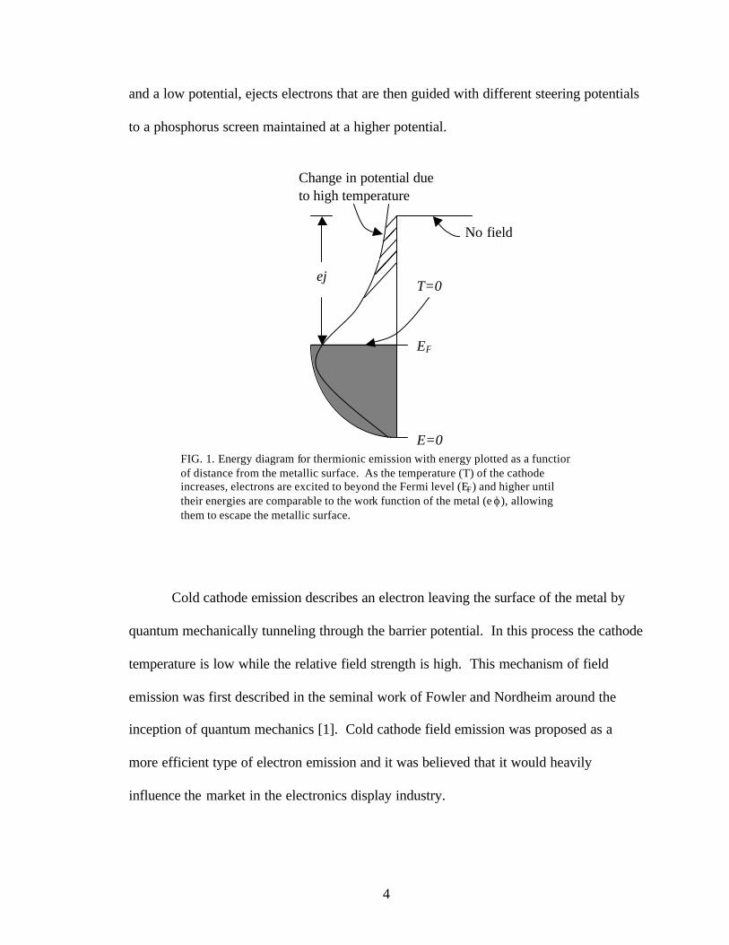
metal. The electron is then free to escape from the metal into the vacuum. Figure 1
shows the process by which this emission takes place, with eϕ representing the work
function of the metal, E representing the energy level of a particular electron, EF as the
Fermi level of the metal, E=0 as the ground state electron on the surface, and the lines in
between as the occupied electron states. Thermionic emission is used, for example, in
cathode ray tubes where a tungsten filament, which is held at several thousand Kelvin
4
and a low potential, ejects electrons that are then guided with different steering potentials
to a phosphorus screen maintained at a higher potential.
Cold cathode emission describes an electron leaving the surface of the metal by
quantum mechanically tunneling through the barrier potential. In this process the cathode
temperature is low while the relative field strength is high. This mechanism of field
emission was first described in the seminal work of Fowler and Nordheim around the
inception of quantum mechanics [1]. Cold cathode field emission was proposed as a
more efficient type of electron emission and it was believed that it would heavily
influence the market in the electronics display industry.
FIG. 1. Energy diagram for thermionic emission with energy plotted as a function of distance from the metallic surface. As the temperature (T) of the cathode increases, electrons are excited to beyond the Fermi level (EF) and higher until their energies are comparable to the work function of the metal (e ϕ), allowing them to escape the metallic surface.
No field
eϕ
EF
E=0
Change in potential due to high temperature
T=0

5
The field emission properties of a metal that has been covered with an adsorbate
has, however, not been studied extensively. When an atom is adsorbed onto the surface
of a metal, an extra bound and vacant electronic state may be created. For example, the
adsorption of oxygen onto molybdenum demonstrates this behavior and has been
summarized previously [2]. The binding energy between a single oxygen atom and
molybdenum (Mo) is greater than the binding energy between the two oxygen atoms in
an oxygen molecule (O2). The O2 will therefore dissociatively adsorb so that the
individual oxygen atoms will occupy sites on the metallic surface [2]. On the surface the
“unoccupied” orbital for an extra electron on the oxygen atom lies below the Fermi level
and hence the atom will reside on the metallic surface as O-. The energy diagram for a
clean cathode surface with a strong extraction field is shown in Figure 2 as a function of
z, the distance from the metal. The schematic for a surface covered with an adsorbate,
such as oxygen, is also illustrated. The new state for O- creates a gap in the previous
barrier potential known as the Schottky barrier (“Field + Surface” in Figure 2) of the
metal and provides a tunneling electron with a decreased thickness through which to
travel (“Field + Surface + Atom” in Figure 2). It has been shown that oxygen coverage
on a molybdenum substrate has a significant effect on the secondary emission of
electrons caused by impacting ions [2]. It was anticipated that adsorbate coverage of the
surface would be strongly correlated to the emission characteristics of Spindt type field
emission cathode arrays [3].

6
1.2 Description of Field Emitter Array
Dr. Capp Spindt and co-workers at Stanford Research Institute (SRI) have used
techniques in thin-film technology and electron beam microlithography to fabricate
cathode arrays of cones [3]. The technique used to produce these field emitter arrays
(FEAs) has been refined to make them with significantly more cones packed into a
smaller area. A schematic of the field emission cathode is illustrated in Figure 3; it
consists of a molybdenum gate film, molybdenum cone, and a silicon substrate. The
molybdenum cones described are each about 1.5 microns tall with a tip radius of about
500 angstroms. They rest on the silicon substrate and a molybdenum gate film surrounds
each one. The cones are exposed through holes in the gate film with a diameter of about
1.5 microns. The gate film and the silicon substrate are isolated from each other via the
silicon dioxide insulating layer [3].
eϕ
z
Field + Surface
Field + Surface + Atom
EF
FIG. 2. Energy diagram for field emission with energy plotted as a function of distance from the metallic surface. “Field + Surface” indicates the lowering of the potential barrier created by the applied electric field. “Field + Surface + Atom” indicates the potential seen by an electron residing on an adsorbate covered metallic surface, with an extra electronic state for O- existing below the Fermi energy.
New state for O-
7
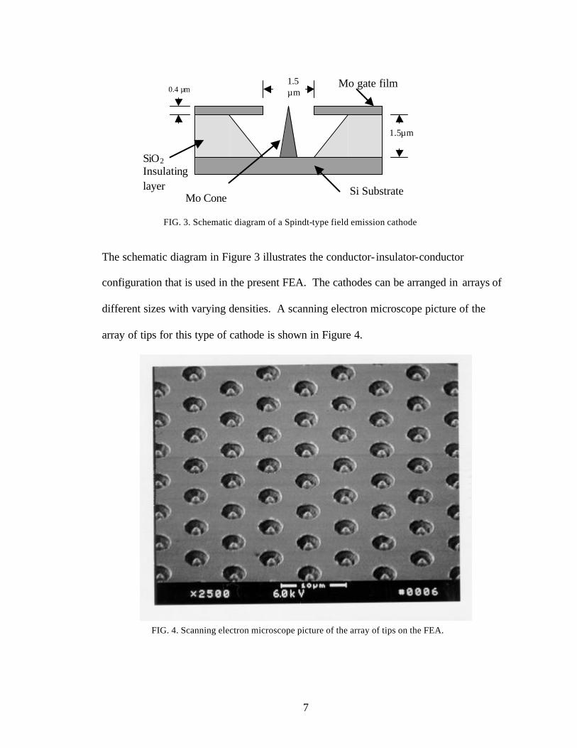
The schematic diagram in Figure 3 illustrates the conductor- insulator-conductor
configuration that is used in the present FEA. The cathodes can be arranged in arrays of
different sizes with varying densities. A scanning electron microscope picture of the
array of tips for this type of cathode is shown in Figure 4.
FIG. 3. Schematic diagram of a Spindt-type field emission cathode
1.5 µm
1.5µm
Mo gate film 0.4 µm
Si Substrate
SiO2 Insulating layer
Mo Cone
FIG. 4. Scanning electron microscope picture of the array of tips on the FEA.
8
Previously used field emitters required a high voltage for operation; the Spindt-
type FEAs operate at a rather low voltage, which provides several advantages. The lower
voltage (of order 100 volts) exposes the FEAs to a lower risk of damage from the
ionization of ambient gas, creating a positive ion that then impacts the tip, in the vacuum
[4]. This means that the FEAs can be used at a higher pressure with a longer operating
lifetime. The FEAs are also reported to have a current density per useful lifetime greater
than that of thermionic cathodes [5]. FEA technologies have been researched in the
display industry as a more efficient alternative to cathode ray tubes (which utilize
thermionic emission) as well as liquid-crystal displays (LCDs) [6]. It is anticipated that
FEAs can function at a lower power than current LCDs and also at a thinner depth than
current flat panel technology [3]. These advantages are very important for technical
applications.
The described geometry of the FEAs is partially responsible for the emission
characteristics. The sharp tips on the cones and the close proximity of the gate allows for
large electric fields to be generated with fairly small voltages. The electrons from the tips
of the cones, where the electric field is the largest, tunnel through the surface barrier of
the metal. The Fowler-Nordheim prediction for emission from the pristine metallic
substrate yields a result that is significantly lower than the observed field emission. It has
been proposed that the enhancement factor is due to adsorbed molecules/atoms on the
surface [3]. Such suggestions, apparently, have not been experimentally examined.
The tips on the surface of the FEAs are highly sensitive and very susceptible to
damage. They cannot be easily heated to temperatures necessary for desorbing residual
molecules from the surface. Research to date does not specify a non-destructive manner
9
in which to clean the tips on the FEAs. Previous experiments have used ion
bombardment with an incident argon ion (Ar+) beam to sputter clean the surface. It is
suspected that this keV ion bombardment may lead to defect formation on the surface of
the tips. After this cleaning, it is supposed that the surface then slowly anneals to the
original topology and thus restores to baseline emission [7]. For the present experiment,
electron-stimulated desorption was used to non-destructively remove adsorbates on the
surface. The electrons, being much less massive than the argon ions, produced less of an
impact that could potentially lead to this defect formation. The ultimate goal of the
experiment was to employ this cleaning technique to characterize the effects that
adsorbate coverage has on the emission characteristics of the FEA.
2. Theory
2.1 Fowler-Nordheim
Fowler-Nordheim theory describes the field emission from an adsorbate free
cathode. The equation relates the field emission current density, J (Amperes per square
centimeter), to the electric field at the surface, E (volts per centimeter), and the work
function of the metal, φ (electron volts), by
−= )v(exp
)(t
2/3
2
2
yE
By
AEJ φφ
A/cm2, (1)
where
A = ×⋅−154 10 6.
A eVV2 , (2)
,eVcmV
1087.63/2
7
⋅×=B and (3)
10
y E= × ⋅
−379 10 4 1 2. //cm
VeV φ . (4)
Both A and B are constant coefficients and y is the Schottky lowering of the work-
function barrier. The lowering and curving of the barrier is due to the image force felt by
an emitted electron near the metal surface. The two functions t(y) and v(y) are elliptic
functions with no units that have been approximated by Spindt [3] to be,
t y2 11( ) .= , and (5)
2-0.95 )v( yy = . (6)
Values for y, t(y), and v(y) have been determined as corrections to the previous work
done by Nordheim [7, 8]. To develop a known expression for Fowler-Nordheim theory,
it is noted that
α/IJ = , and (7)
E V d= β / , (8)
where I is current measured in Amperes, a is the emitting area in units of square
centimeters, ß is a unitless field enhancement factor due to the geometry, V is the applied
voltage measured in volts, and d is the gap dimension in centimeters. Substituting these
values into Eq. (1) and redefining constants yields
−=
Vb
aVI exp2 , (9)
where
aA
dBd
V=
×
−α βφ
φβ
2
2
3 2 7
11144 10
.exp
( . )/
and (10)
bBd
=0 95 3 2. /φ
β.
11
In Eq. (9) a depends on the emitting surface area and b depends on the shape and radius
of the tips [3]. Eq. (9) can be rearranged to yield
Vb
VaI
−=
⋅ 2ln (11)
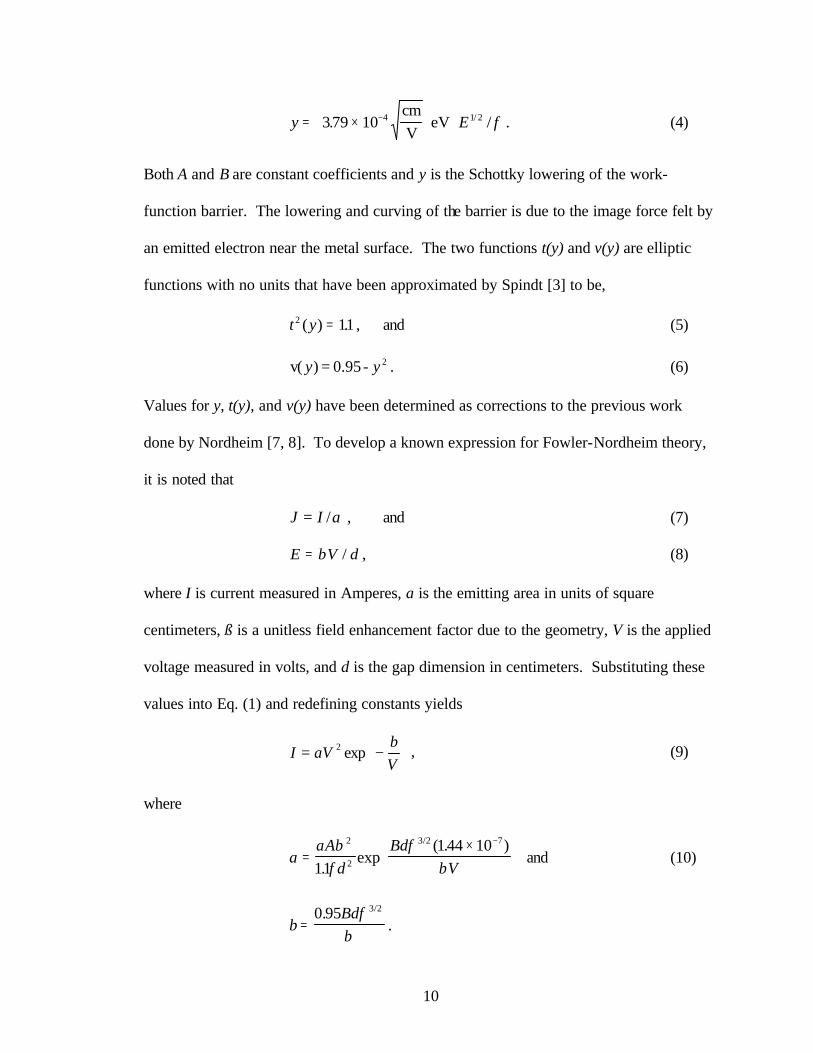
which shows a linear relationship between the natural logarithm of (I/V2) and (1/V). This
relation, known as a Fowler-Nordheim plot, yields a straight line while experimental data
varies slightly from the model both when the field emitter just begins to emit and at the
high end of emission. The Fowler-Nordheim plot for the cathode used in this experiment
is shown in Figure 5.
FIG. 5. Fowler-Nordheim plot provided with FEA from SRI International. This plot shows the linear relationship between the inverse of the Bias-Gate Voltage and the natural logarithm of (emission current/ Bias-Gate Voltage2).
1000/(Bias-Gate Voltage) (V-1)

12
2.2 Electron-Stimulated Desorption
The cleaning of the tips for this experiment was facilitated by electron-stimulated
desorption (ESD). In this process, an electron impact results in the excitation of an
adsorbed atom or molecule on the surface of a metal. This new species can be formed in
an anti-bonding state, as illustrated in Figure 6, and will have a different interaction
energy with the metallic surface than the former adsorbed species. Desorption occurs as
the excited species moves away from the surface and gains kinetic energy from the
potential energy loss. This process is seen in Figure 6 with energy plotted as a function
of distance from the metallic surface [9].
If the desorption of adsorbates on the surface is due solely to ESD, the decrease in
the desorption density, dN, is directly proportional to the number of incident electrons per
FIG. 6. Energy diagram showing the ESD process with energy plotted as a function of distance from the metallic surface. An incident electron impacting the metal excites an adsorbed species residing on the surface. The energy transfer involved results in the desorption of the adsorbate.
13
unit area and time, n, the amount of adsorbate per unit area, N, and the time, dt. The
proportionality constant is usually called the cross section and is denoted by σ.
Hence,
dNN
ndt= − σ . (12)
This differential equation for the adsorbate coverage can be solved to yield
N N t= −0 exp( / )τ , (13)
where the decay rate is denoted by
τσ
=1n
. (14)
Previous experiments with ESD have yielded results for the desorption cross section, σ,
to be on the order of 10-17 square centimeters or 0.1 square angstroms [10]. The
adsorbate coverage after cleaning can therefore be estimated from Eq. (13) given the
initial coverage, number of electrons per unit area and time, and the time of exposure.
3. Experimental Procedure
The chamber for the experiment is an ultrahigh vacuum (UHV) operating in the
range of about 10-9 torr. This high vacuum was necessary for this experiment so that the
state of the surface could be more precisely controlled. The specific cathode used in this
experiment also requires a UHV environment for operation. An apparatus was set up in
the chamber with the cathode, consisting of the FEA and a TO-5 header, mounted onto a
moveable armature in the center as shown by the dotted lines in Figure 7. The moving
armature allowed for the cathode to be positioned on the horizontal, facing the electron
gun for cleaning, as well as rotated 45 degrees from the horizontal to face a
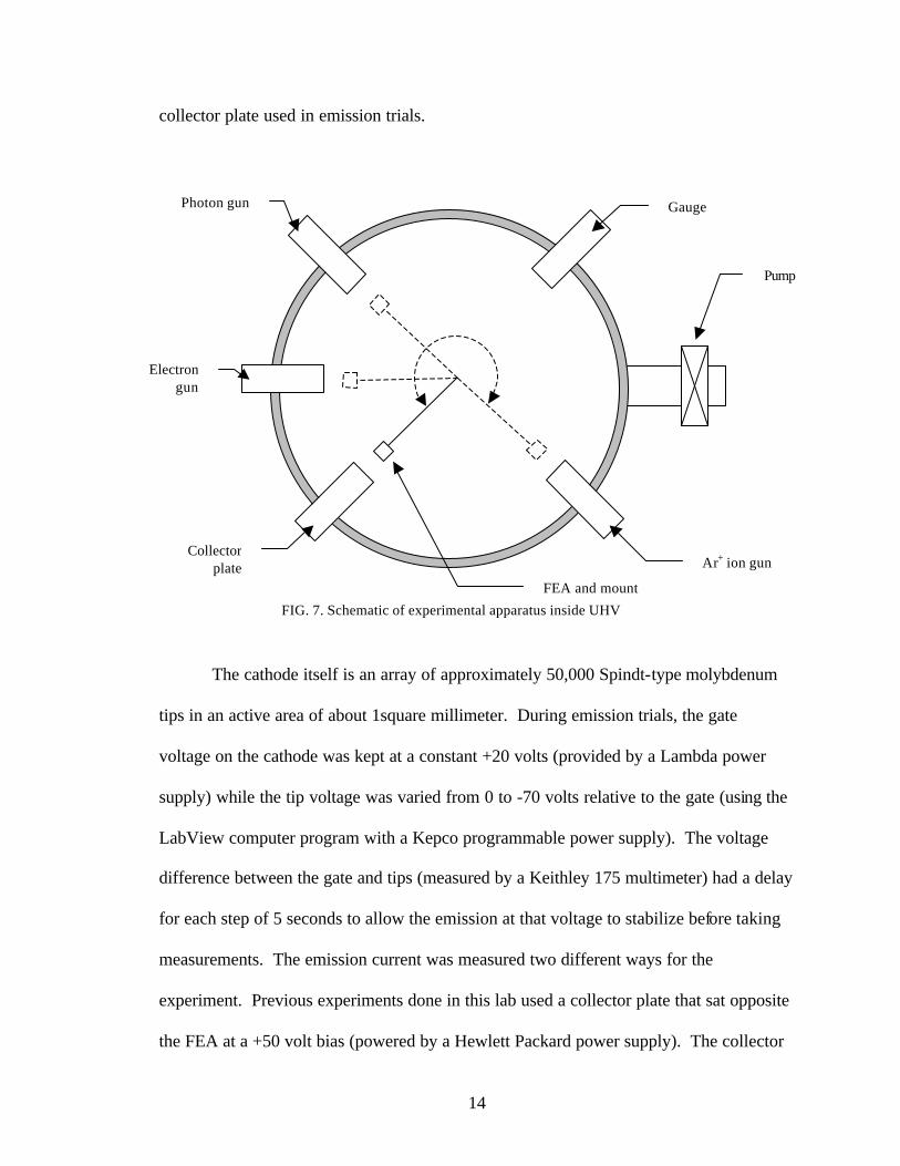
14
collector plate used in emission trials.
The cathode itself is an array of approximately 50,000 Spindt-type molybdenum
tips in an active area of about 1square millimeter. During emission trials, the gate
voltage on the cathode was kept at a constant +20 volts (provided by a Lambda power
supply) while the tip voltage was varied from 0 to 70 volts relative to the gate (using the
LabView computer program with a Kepco programmable power supply). The voltage
difference between the gate and tips (measured by a Keithley 175 multimeter) had a delay
for each step of 5 seconds to allow the emission at that voltage to stabilize before taking
measurements. The emission current was measured two different ways for the
experiment. Previous experiments done in this lab used a collector plate that sat opposite
the FEA at a +50 volt bias (powered by a Hewlett Packard power supply). The collector
Pump
Collector plate
Electron gun
Photon gun
FEA and mount
Ar+ ion gun
Gauge
FIG. 7. Schematic of experimental apparatus inside UHV

15
plate was 1- inch by 1- inch and slightly curved up towards the FEA to improve the
accuracy of the measurement. Due to the different cleaning mechanisms used for this
experiment, a brass shield was later added to the FEA, surrounding the active emitting
area. The shield acted as a new collector plate, also biased at a +50 volts, for early trials
in this experiment. Later trials utilized both the old collector plate and the new shield as
a combined new collector. The current to the collector and shield arrangement was
determined for each voltage step between the gate and tips (amplified by an SRS model
SR570 low-noise current preamplifier and measured by a Fluke 45 dual display
multimeter). An example of a typical curve for the combined current measured at both
collector and shield plotted as a function of the relative gate-tip voltage is shown in
Figure 8. This figure shows that emission begins in the range of 35-40 volts and
increases exponentially from there.
20 30 40 50 60 700.0
0.2
0.4
0.6
0.8
1.0
1.2
Cur
rent
(µΑ
)
Gate-Tip Voltage (V)
baseline
FIG. 8. Collector current as a function of gate-tip voltage

16
The cleaning procedure consisted of directing a beam of electrons at the tips of
the cathode to facilitate the ESD process. With the right conditions the interaction of the
electrons with the FEA surface caused the removal of the adsorbates on the tips. To
employ ESD, an electron gun was used to direct a beam of electrons with energy of 1
keV to the tips to deliver a current of approximately – 0.1 microamperes.
The design of the FEA and TO-5 header is such that it is not possible to
electrically isolate either the tips or the gate. The tips are connected to the TO-5 header,
which is connected to the casing for the mount. This aspect of the design proved to be a
problem for this experiment in particular where it is necessary to measure the current
delivered solely to the tips in the cleaning process. A brass shield 1- inch in diameter with
a circular hole comparable to the square millimeter active emitting area on the FEA was
attached to - but electrically isolated from - the TO-5 header so that the hole coincided
with the active emitting area, as illustrated in Figure 9. This acted as a shield so that
when measuring current delivered to the tips, current from the casing would not also be
taken into account. This new shield provided a way to accurately measure the current
delivered to the tips and was also used in the collector arrangement for measuring
emission current from the FEA.

17
The experimental procedure described was used to first measure the emission of
the FEA, clean the surface, and again measure the emission. It was anticipated that this
process would result in a change in the emission characteristics after cleaning, possibly
reducing field emission, indicating that an adsorbate on the surface is responsible for the
emission characteristics. This experimental procedure was repeated many times and the
data showed this hypothesis to be accurate.
4. Results and Discussion
4.1 Cleaning Trials
The FEA and mount was placed into the vacuum chamber, first under technical
vacuum conditions. The experiment was carried out once an ideal pressure of about 10-9
torr was established. Early experiments were carried out to determine safe operating
FIG. 9. Schematic of FEA, TO-5 header, mount for FEA, and added brass shield
TO-5 header (common to the tips)
Active emitting area (1 mm2)
Brass shield
Insulating material Mount and casing for FEA
18
voltages to the tips and gate on the FEA as well as to the collector plate arrangement.
Initial emission tests showed the baseline curve that is characteristic of the FEA. Once
this curve was established, proper cleaning intervals were determined. The first
successful cleaning trial was found to be with an electron beam energy of 1 keV
delivering a current of – 0.1 microamperes to the tips of the FEA for one hour. This data
was taken with only the shield surrounding the emitting area acting as the collector plate.
This current and time can be used to find the total number of electrons impacting the tips
by
011
101
16 103600 2 25 106 19
15./ sec
/ sec .sec .µ
µA
CC
eC
× ××
× = ×− e. (15)
Noting that there are a total of 50,000 tips on the FEA, the number of electrons impacting
each tip is found to be 4 5 1010. × . The specifications of the FEA indicate that the opening
in the gate film to one of the tips has a diameter of about 1.5 microns [3]. The area is
thus determined to be
Area = 18 108. × C2/opening. (16)
Using Eqs. (15) and (16) and the total number of tips as 50,000, the number of electron
impacts per area in one hour is found to be approximately 250 electrons per square
angstrom.
Given this cleaning interval and an initial adsorbate coverage, the resulting
coverage can be solved for by first noting from Eqs. (15) and (16) that n = 0.069
electrons per second per square angstrom. If σ = 01. square angstroms, as experimental
results have shown [10], then the characteristic decay rate from Eq. (14) will be
τσ
≅ ≅1
144n
sec . (17)

19
If the ESD occurs for a time t = 3600 seconds, t /τ = 25, which when substituted into Eq.
(13) yields
NN
t0
25= − = −exp( / ) exp( )τ = 14 10 11. × − , (18)
indicating that the adsorbate concentration on the surface should be substantially reduced.
This simple analysis for determining coverage after cleaning does not take into account
the readsorption of adsorbates to the surface during cleaning and after cleaning has
ended. The unit of gas exposure is called a Langmuir (L) and it corresponds to 10-6
torr·seconds of exposure. An exposure of 1L would result in approximately one
monolayer of coverage (i.e., ˜ 1015 per square centimeter) if all impacting
molecules/atoms stuck to the surface. Hence if the probability of that adsorbate sticking
to the surface is known, the amount of adsorbate coverage can be determined. With a
background pressure of about 5 10 9× − torr as in this experiment, assuming unit sticking
probability, the time to acquire one monolayer is about 500 seconds.
We can modify Eq. (12) to approximately account for adsorption:
dN Nn dtN N
NN psdt= − +
−
σ 0
00 . (19)
The additional term contains the adsorption rate, N0ps, where p is expressed in units of
10-6 torr and s is the sticking probability for the surface ( 0 1≤ ≤s ). The term in brackets
represents the fraction of the sites available for adsorption to occur. Full coverage is
designated by N0. The solution to Eq. (19) is
N tN
psps
ps tps
ps( )
exp[ ( ) ]0
1= −+
− + +
+ββ
β , (20)
where

20
β σ= n . (21)
For our experiment, β ≅ 0.0069 and p ≅ 0.005. For molybdenum the sticking probability
has been determined to be s = 0.1 [2], thus the asymptotic coverage, N(4)/N0, is found
from Eq. (20) to be about 7%. In this experiment, species re-adsorption is clearly
important, but at the same time Eq. (20) indicates that the ESD process should
undoubtedly clean the surface of the FEA to a significant extent (about 93%).
The first cleaning of an FEA exposed to atmospheric pressure resulted in a slight
increase in the emission from baseline levels as seen in Figure 10 (for this particular data
set the shield acted as the collector). The increase in emission can be explained by noting
that cleaning the emitter after it has been exposed to the atmosphere will possibly remove
top layer(s) of adsorbates from the surface. The tips are now cleaner but residual
adsorbates still exist on the surface. After this preliminary adsorbate removal, the
cathode was allowed to relax for a period of 30 minutes. During this interval, it can be
seen that the emission started to return to the baseline level as the species cleaned from
the surface once again adsorbed to the tips, thus inhibiting emission.

21
20 30 40 50 60 700.0
0.1
0.2
0.3
0.4
0.5
0.6
0.7
0.8 baseline after atmospheric exposure clean 1hr with -0.1µΑ to tips 30 min relaxation
Cur
rent
(µΑ
)
Gate-Tip Voltage (V)
Once this relationship had been established, further adsorbate removal was
accomplished via a second stage of electron- initiated ESD. The initial stage of cleaning
facilitated the removal of adsorbates that inhibited emission; the second stage removed
additional adsorbates from the surface and the emission was seen to decrease as
illustrated in Figure 11. A characteristic baseline curve was taken for the FEA after stage
one cleaning and once again a 1 keV electron beam was directed at the tips so as to
provide a current of about – 0.1 microamperes. A one-hour cleaning interval with these
conditions resulted in a decrease in emission shown in Figure 11.
FIG. 10. Voltage versus collector current for initial cleaning trial. The black curve indicates the emission curve upon first placing the FEA into UHV conditions. The red curve shows an increase in emission after using ESD to clean the tips for one hour with a current of – 0.1µA to the tips. The green curve shows a slow return to baseline levels after a 30-minute period of relaxation. This indicates that initial cleaning of the surface removed adsorbates that inhibit emission which then readsorb to the surface after cleaning bringing the emission back down to near baseline levels.

22
20 30 40 50 60 700.0
0.2
0.4
0.6
0.8
1.0
Cur
rent
(µΑ
)
Gate-Tip Voltage (V)
overnight baseline at 10-9 torr clean 1hr with -0.1µΑ to tips
The decrease in emission from baseline levels is presumably due to the removal of the
emission enhancing adsorbates from the surface as discussed in section 1.2. The red
curve shows the emission from a relatively clean cathode surface. After relaxation of the
cathode, the desorbed species readsorb to the surface, once again restoring emission.
4.2 Cathode Failure
During this investigation of the emission properties of the FEA, two separate
cathodes were used. The experimental procedure was refined in an attempt to ensure that
the cathode was not damaged during operation. Although precautions were taken with
each step of the process, two different cathodes failed catastrophically during the
FIG. 11. Voltage versus collector current for next cleaning trial. The black curve shows the characteristic emission after initial cleaning had been performed. The red curve shows the reduction in emission after further cleaning of tips, indicating the removal of the adsorbate responsible for the high emission properties.

23
investigation. The first cathode failure occurred after a period of dormancy in the
vacuum; it is not known what precisely caused this failure. All of the data in this analysis
was taken from the second cathode used. During the last cleaning trial, the second
cathode was subjected to a voltage exceeding its limit (about 70 volts in this experiment)
due to a faulty power supply. Once a cathode fails to function properly, a resistance on
the order of a megaohm can be detected between the tips and the gate structure. The first
cathode showed a resistance of about 6 megaohms after failure while the second had a
resistance of 1.5 megaohms. A scanning electron microscope (SEM) was used to
examine the array structure of each cathode after the failures occurred to verify the
failures.
The first cathode failed in early October before the experimental procedure had
been tested. With the SEM, the cathode showed the usual array of cones in the active
area, however several of the cones appeared to be missing as seen in Figure 12. Further
analysis of the structure showed one of these displaced cones from the array, which can
be seen in Figure 13. It is not clear what caused this damage, as the cathode was not in
operation for a period of two weeks prior to discovery of the failure. Before this inactive
period, the cathode was fully operational.
24
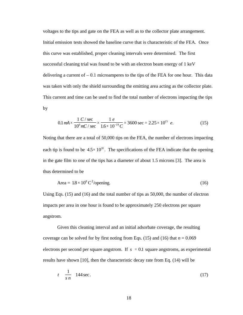
FIG. 12. SEM picture of array of first cathode used in the experiment. This shows the array of cones in the gate structure, however many of the cones appear to be missing, indicated by the dark holes.
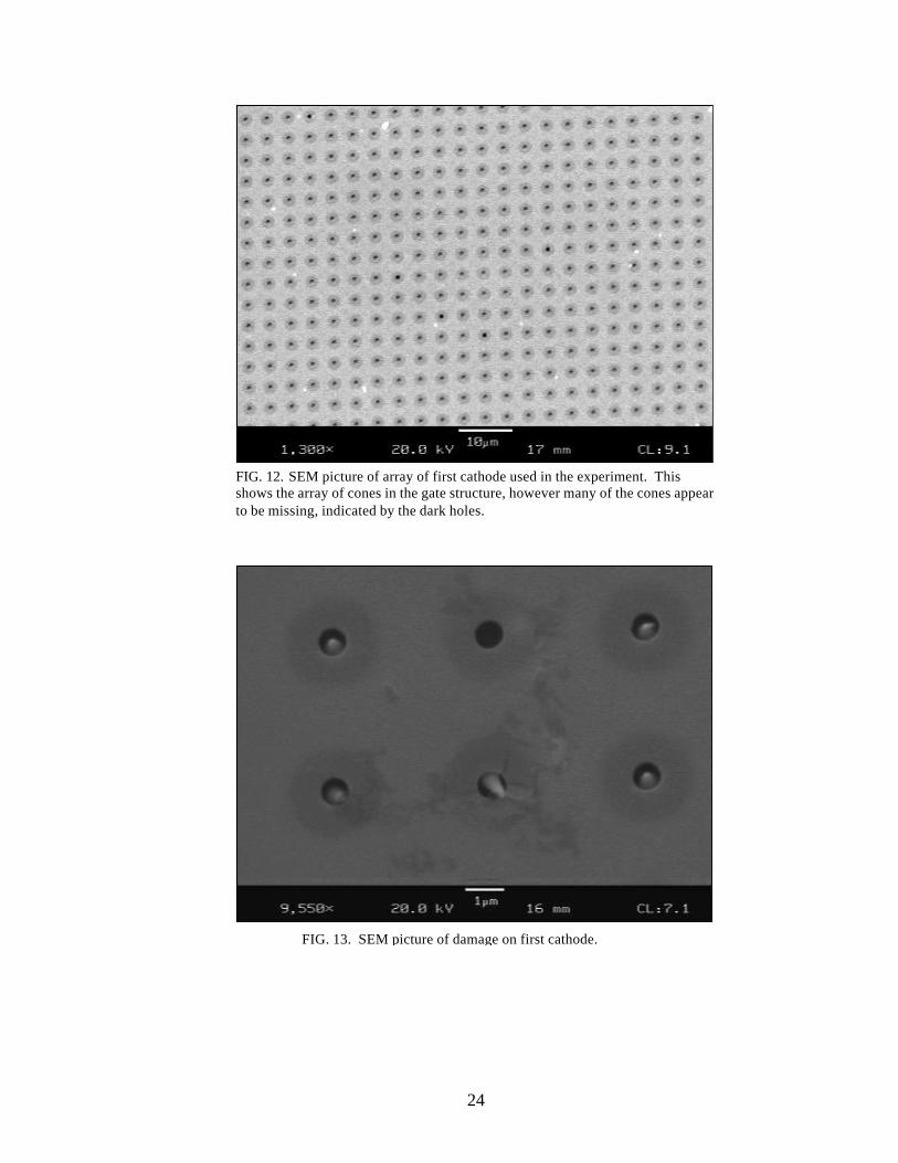
FIG. 13. SEM picture of damage on first cathode.
25
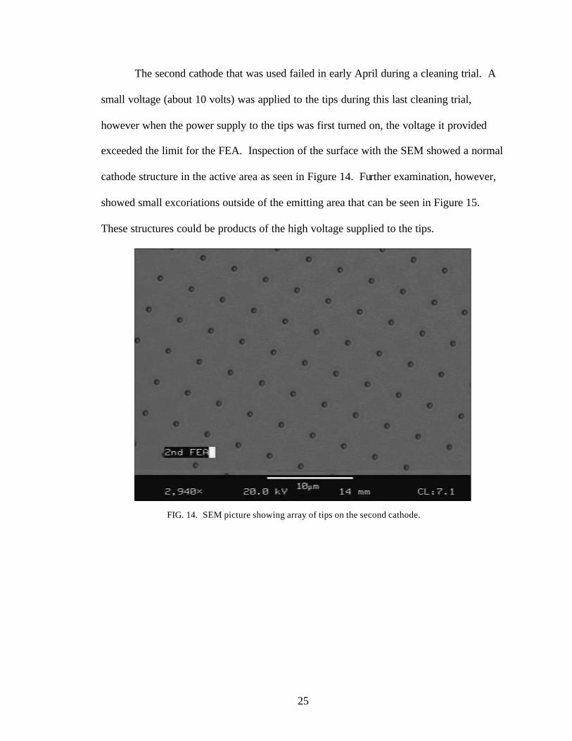
The second cathode that was used failed in early April during a cleaning trial. A
small voltage (about 10 volts) was applied to the tips during this last cleaning trial,
however when the power supply to the tips was first turned on, the voltage it provided
exceeded the limit for the FEA. Inspection of the surface with the SEM showed a normal
cathode structure in the active area as seen in Figure 14. Further examination, however,
showed small excoriations outside of the emitting area that can be seen in Figure 15.
These structures could be products of the high voltage supplied to the tips.
FIG. 14. SEM picture showing array of tips on the second cathode.

26
5. Conclusions and Future Work
The goal of this experiment was to determine the correlation between adsorbate
coverage and emission properties of a Spindt-type molybdenum cathode FEA. To
determine this relationship, the emission properties of an adsorbate free surface had to be
characterized. ESD was employed as the cleaning technique to accomplish a non-
destructive removal of adsorbates from the tips of the FEA. Ultimately, it was found that
initial ESD cleaning of the tips proved to enhance the emission characteristics from
beyond the baseline level while further cleaning reduced emission to below baseline
levels, showing that adsorbates have a significant effect on emission properties.
Relaxation periods after cleaning trials showed that the cathode slowly returned to
FIG. 15. SEM picture of a small excoriation found outside of the emitting area on the second cathode.

27
baseline levels, indicating that there is a gradual readsorption to the surface from
previously removed adsorbates.
Once this relationship had been established, the results were compared to the
Fowler-Nordheim model given in Eq. (11). Taking a curve of the emission
characteristics after initial cleaning results in a Fowler-Nordheim plot as seen in Figure
16. The Fowler-Nordheim equation shows the emission from just one of the cones on the
FEA. It does not apply to each cone, as it does not take into account that the cones may
vary slightly in size and some may have sharper tips than others. The specifications are
for the average of the properties of all of the 50,000 tips. This is likely to be why the
Fowler-Nordheim plot for this situation deviates from what is predicted to be a straight
line.
14 15 16 17 18 19 20 21-9.0
-8.9
-8.8
-8.7
-8.6
-8.5
-8.4
-8.3
-8.2
-8.1
-8.0
ln(I
/V2 )
1000/Gate-Tip Voltage (V-1)
baseline after atmospheric clean1 30 min relaxation
FIG. 16. Fowler-Nordheim plot for initial cleaning of cathode. The black curve shows the baseline level after being exposed to the atmosphere, the red curve shows emission after using ESD to clean the cathode for 1 hour delivering 0.1µA to the tips. The green curve shows the emission after a 30-minute period of relaxation after cleaning the tips. Clearly, the emission increases after initial cleaning and then decreases back to baseline levels after the removed adsorbates reattach to the surface.
28
The specified experiment shows that a clean cathode surface has different
emission characteristics than that of an adsorbate-covered surface. Certain adsorbates on
the surface reduce emission while others serve to enhance emission. A possible model
demonstrating this behavior could be that a surface with multiple layers does not produce
much emission, a surface with a monolayer of coverage shows an enhancement in
emission, and a clean cathode surface produces emission that is characteristic of the
Fowler-Nordheim model. Further work in this area can be done to determine the
correctness of this model. Now that a non-destructive cleaning procedure has been
established, the types of adsorbates that inhibit and promote field emission can be
determined. Trace gases that exist in the vacuum chamber that should be tested include
oxygen, hydrogen, methane, carbon dioxide, and water. After cleaning the surface,
various exposures of the trace gases could be utilized to determine what effects, if any,
they have on the emission. If the tested adsorbate enhances the field emission, the
characteristic curve should return to pre-cleaning baseline levels.
29
6. Acknowledgements
I would like to thank my advisor, Dr. Roy Champion, and Wendy Vogan for their
assistance on completing this experiment and thesis. Special thanks also to Dr. Gina
Hoatson, Dr. Todd Averett, and Dr. Vladimir Bolotnikov for serving on my committee.

30
7. References
[1] R. H. Fowler, F.R.S., L. Nordheim, Proc. Roy. Soc. London A119 (1928) 173. [2] J. C. Tucek, S. G. Walton, R. L. Champion, Surf. Sci. 410 (1998) 258 – 269. [3] C. A. Spindt, I. Brodie, L. Humphrey, E. R. Westerberg, J. Appl. Phys. 47 (1976)
5248. [4] I. Brodie, Int’l J. Electron. 38 (1975) 541. [5] A. H. W. Beck, Proc. IEEE. 106B (1959) 372. [6] T. S. Fahlen, SPIE Proc. 3636 (1999) 124 – 130. [7] J. C. Miller, “The Role of Adsorbates on Field Emission,” Senior Thesis, The
College of William and Mary (2002) [8] R. E. Burgess, H. Kroemer, J. M. Houston, Phys. Rev. 90 (1953) 515. [9] Q. Li, “An Introduction to ESD – Electron Stimulated Desorption,”
http://www.chembio.uoguelph.ca/educmat/chm729/esdiad/button.htm (April 10, 2003).
[10] K. Suzuki, S. Kobayashi, T. Katsube, Applied Surface Science 33/34 (1988) 325-334.