admittance smith chart high frequency network …mshashmi/rfcd_2017/lecture_slides/lect_7_2017.pdfzy...
TRANSCRIPT
Indraprastha Institute of
Information Technology Delhi ECE321/521
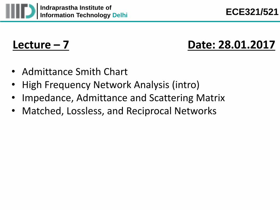
Lecture – 7 Date: 28.01.2017
• Admittance Smith Chart • High Frequency Network Analysis (intro) • Impedance, Admittance and Scattering Matrix • Matched, Lossless, and Reciprocal Networks
Indraprastha Institute of
Information Technology Delhi ECE321/521
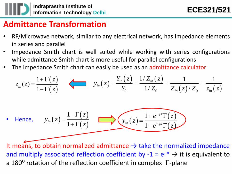
Admittance Transformation
• RF/Microwave network, similar to any electrical network, has impedance elementsin series and parallel
• Impedance Smith chart is well suited while working with series configurationswhile admittance Smith chart is more useful for parallel configurations
• The impedance Smith chart can easily be used as an admittance calculator
1( )
1in
zz z
z
1
1in
zy z
z
• Hence,
0 0 0
1/ 1 1
1/ /
in in
in
in in
Y z Z zy z
Y Z Z z Z z z
1
1
j
in j
e zy z
e z
It means, to obtain normalized admittance → take the normalized impedanceand multiply associated reflection coefficient by -1 = e-jπ → it is equivalent toa 180⁰ rotation of the reflection coefficient in complex Γ-plane
Indraprastha Institute of
Information Technology Delhi ECE321/521
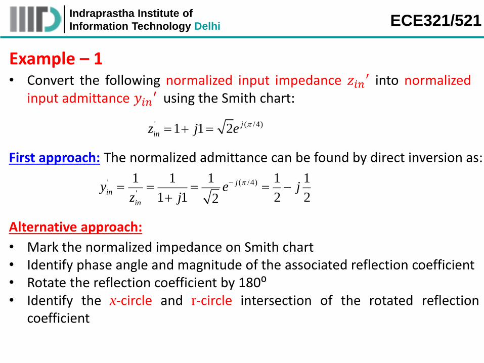
Example – 1 • Convert the following normalized input impedance 𝑧𝑖𝑛
′ into normalizedinput admittance 𝑦𝑖𝑛
′ using the Smith chart:
' ( /4)1 1 2 j
inz j e
First approach: The normalized admittance can be found by direct inversion as:
' ( /4)
'
1 1 1 1 1
1 1 2 22
j
in
in
y e jz j
Alternative approach:
• Mark the normalized impedance on Smith chart • Identify phase angle and magnitude of the associated reflection coefficient • Rotate the reflection coefficient by 180⁰• Identify the x-circle and r-circle intersection of the rotated reflection
coefficient

Indraprastha Institute of
Information Technology Delhi ECE321/521
Example – 1 (contd.) Normalized impedance (zin’) is the intersection of r-circleof 1 and x-circle of 1
Rotate this by 180⁰ to obtain normalized
admittance
Quick investigation shows that the
normalized impedance (yin’ ) is the intersection of r-circle of 1/2 and
x-circle of -1/2
To denormalize, multiply with the inverse of Z0.
' '
0
0
1in in inY y Y y
Z
Indraprastha Institute of
Information Technology Delhi ECE321/521
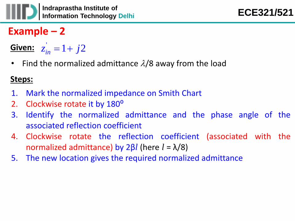
Example – 2
• Find the normalized admittance l/8 away from the load
' 1 2 inz j Given:
1. Mark the normalized impedance on Smith Chart2. Clockwise rotate it by 180⁰3. Identify the normalized admittance and the phase angle of the
associated reflection coefficient4. Clockwise rotate the reflection coefficient (associated with the
normalized admittance) by 2βl (here l = λ/8)5. The new location gives the required normalized admittance
Steps:

Indraprastha Institute of
Information Technology Delhi ECE321/521
Example – 2 (contd.)
' 0.2 .4 0iny j
' 1 2 inz j ' 0.20 0.40 iny j
2 4l
l l
Clockwise rotation by
o/ 8 2 90l ll
180⁰ clockwise rotation
Indraprastha Institute of
Information Technology Delhi ECE321/521
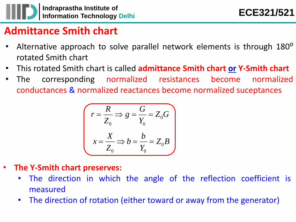
Admittance Smith chart
• Alternative approach to solve parallel network elements is through 180⁰rotated Smith chart
• This rotated Smith chart is called admittance Smith chart or Y-Smith chart• The corresponding normalized resistances become normalized
conductances & normalized reactances become normalized suceptances
0
0 0
R Gr g Z G
Z Y
0
0 0
X bx b Z B
Z Y
• The Y-Smith chart preserves:• The direction in which the angle of the reflection coefficient is
measured• The direction of rotation (either toward or away from the generator)
Indraprastha Institute of
Information Technology Delhi ECE321/521
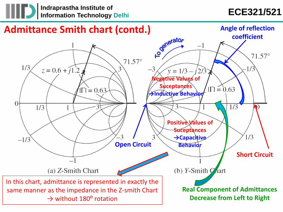
Admittance Smith chart (contd.)
Open Circuit
Short Circuit
Negative Values of Suceptances
→Inductive Behavior
Positive Values of Suceptances→Capacitive
Behavior
Real Component of Admittances Decrease from Left to Right
Angle of reflection coefficient
In this chart, admittance is represented in exactly the same manner as the impedance in the Z-smith Chart
→ without 180⁰ rotation

Indraprastha Institute of
Information Technology Delhi ECE321/521
Combined Z- and Y- Smith Charts
Red: Z – Smith Chart
Blue: Y – Smith Chart

Indraprastha Institute of
Information Technology Delhi ECE321/521
Example – 3• Identify (a) the normalized impedance z’ = 0.5 + j0.5, and (b) the normalized
admittance value y’ = 1 + j2 in the combined ZY-Smith Chart and find thecorresponding values of normalized admittance and impedance
' 0.5 0.5z j
' 1 2y j
' 1 1y j
' 0.2 0.4z j
Indraprastha Institute of
Information Technology Delhi ECE321/521
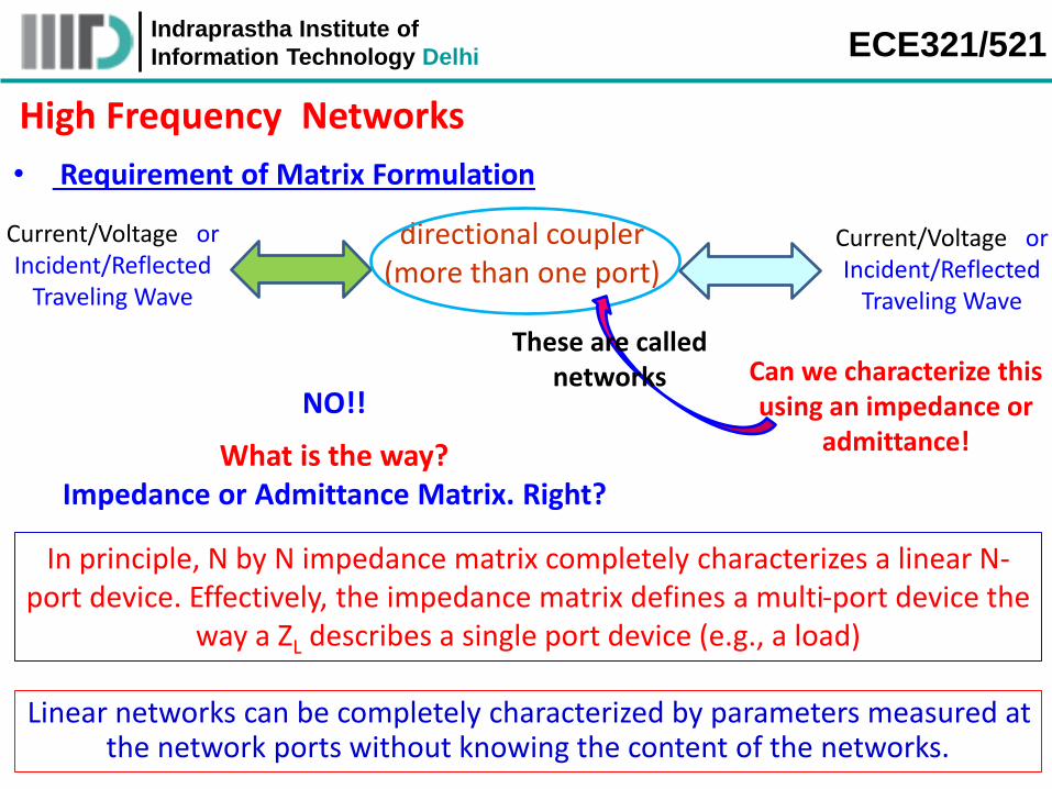
• Requirement of Matrix Formulation
directional coupler(more than one port)
Current/Voltage or Incident/Reflected
Traveling Wave
Current/Voltage or Incident/Reflected
Traveling Wave
NO!!
What is the way? Impedance or Admittance Matrix. Right?
In principle, N by N impedance matrix completely characterizes a linear N-port device. Effectively, the impedance matrix defines a multi-port device the
way a ZL describes a single port device (e.g., a load)
Linear networks can be completely characterized by parameters measured at the network ports without knowing the content of the networks.
High Frequency Networks
These are called networks Can we characterize this
using an impedance or admittance!
Indraprastha Institute of
Information Technology Delhi ECE321/521
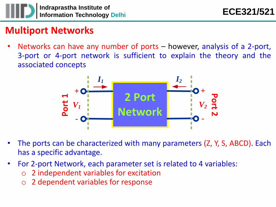
Multiport Networks
• Networks can have any number of ports – however, analysis of a 2-port,3-port or 4-port network is sufficient to explain the theory and theassociated concepts
2 PortNetworkP
ort
1
I1
+
-
V1
Po
rt 2
I2
+
-
V2
• The ports can be characterized with many parameters (Z, Y, S, ABCD). Eachhas a specific advantage.
• For 2-port Network, each parameter set is related to 4 variables:o 2 independent variables for excitationo 2 dependent variables for response
Indraprastha Institute of
Information Technology Delhi ECE321/521
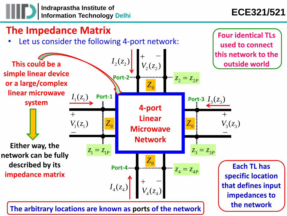
The Impedance Matrix• Let us consider the following 4-port network:
4-port Linear
Microwave Network
1 1( )V z
3 3( )V z
4 4( )V z
2 2( )V z
1 1( )I z3 3( )I z
2 2( )I z
4 4( )I z
Port-1
Port-4
Port-3
Port-2
3 3Pz z
4 4Pz z
2 2Pz z
1 1Pz z
0Z
0Z0Z
0Z
Either way, the network can be fully
described by its impedance matrix
Each TL has specific location
that defines input impedances to
the networkThe arbitrary locations are known as ports of the network
This could be a simple linear device or a large/complex linear microwave
system
Four identical TLs used to connect
this network to the outside world

Indraprastha Institute of
Information Technology Delhi ECE321/521
The Impedance Matrix (contd.)• In principle, the current and voltages at
the port-n of networks are given as:
• In order to define the elements of impedance matrix, there will beneed to measure/determine the associated voltages and currents atthe respective ports. Suppose, if we measure/determine current atport-1 and then voltage at port-2 then we can define:
221
1
VZ
I
Trans-impedance
( )n n nPV z z ( )n n nPI z z
• However, the simplifiedformulations are:
( )n n n nPV V z z ( )n n n nPI I z z
• If we want to say that there exists a non-zerocurrent at port-1 and zero current at all otherports then we can write as:
1 0I 2 3 4 0I I I
• Similarly, the trans-impedanceparameters Z31 and Z41 are:
331
1
VZ
I
441
1
VZ
I
• We can also define other trans-impedance parameters such as Z34 as the ratiobetween the complex values I4 (the current into port-4) and V3 (the voltage atport-3), given that the currents at all other ports (1, 2, and 3) are zero.

Indraprastha Institute of
Information Technology Delhi ECE321/521
The Impedance Matrix (contd.)
How do we ensure that all but one port current is zero?
• Therefore, the more genericform of trans-impedance is:
mmn
n
VZ
I (given that Ik = 0 for all k≠n)
4-port Linear Microwave
Network
0Z
0Z0Z
0Z
1V
1I
Port-1
4V 4 0I Port-4
3V
3 0I
Port-3
2V
2 0I Port-2• Open the portswhere the currentneeds to be zero:
The ports should be opened! not
the TL connected to the ports
• then define the respectivetrans-impedances as:
mmn
n
VZ
I (given that all ports k≠n are open)

Indraprastha Institute of
Information Technology Delhi ECE321/521
The Impedance Matrix (contd.)• Once we have defined the trans-impedance terms by opening various ports, it is
time to formulate the impedance matrix• Since the network is linear, the voltage at any port due to all the port currents is
simply the coherent sum of the voltage at that port due to each of the currents
1
N
m mn n
n
V Z I
• Therefore we can generalize the
voltage for N-port network as:V = ZI
• Where I and V arevectors given as:
1 2 3 NV , V , V , ...., VV =T
1 2 3 NI , I , I , ...., II =T
3 34 4 33 3 32 2 31 1V Z I Z I Z I Z I • For example, the voltage at port-3 is:
• The term Z is matrix given by:
11 12 1
21
1 2
n
m m mn
Z Z Z
Z
Z Z Z
Z Impedance Matrix
• The values of elements in the impedancematrix are frequency dependents and often itis advisable to describe impedance matrix as:
11 12 1
21
1 2
( ) ( ) ( )
( )
( ) ( ) ( )
n
m m mn
Z Z Z
Z
Z Z Z
Z( )
Indraprastha Institute of
Information Technology Delhi ECE321/521
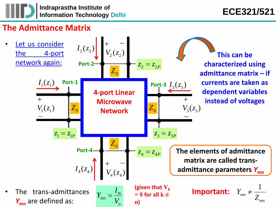
The Admittance Matrix
4-port Linear Microwave
Network1 1( )V z
3 3( )V z
4 4( )V z
2 2( )V z
1 1( )I z3 3( )I z
2 2( )I z
4 4( )I z
Port-1
Port-4
Port-3
Port-2
3 3Pz z
4 4Pz z
2 2Pz z
1 1Pz z
0Z
0Z0Z
0Z
This can be characterized using
admittance matrix – if currents are taken as dependent variables instead of voltages
The elements of admittance matrix are called trans-
admittance parameters Ymn
• Let us considerthe 4-portnetwork again:
• The trans-admittancesYmn are defined as:
mmn
n
IY
V
(given that Vk
= 0 for all k ≠
n)
1mn
mn
YZ
Important:
Indraprastha Institute of
Information Technology Delhi ECE321/521
4-port Linear Microwave
Network
0Z
0Z0Z
0Z
1V
1I
Port-1
4 0V 4I Port-4
3 0V
3I
Port-3
2 0V 2I Port-2• the voltage at all but one port
must be equal to zero. This canbe ensured by short-circuitingthe voltage ports.
The Admittance Matrix (contd.)
The ports should be short-circuited! not the TL
connected to the ports
• Now, since the network is linear, the current at any one port due to all the portvoltages is simply the coherent sum of the currents at that port due to each ofthe port voltages.
• For example, the current at port-3 is:3 34 4 33 3 32 2 31 1I Y V Y V Y V Y V
• Therefore we can generalize thecurrent for N-port network as:
1
N
m mn n
n
I Y V
I = YV
Indraprastha Institute of
Information Technology Delhi ECE321/521
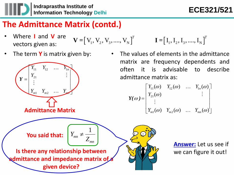
The Admittance Matrix (contd.)• Where I and V are
vectors given as: 1 2 3 NV , V , V , ...., VV =
T
1 2 3 NI , I , I , ...., II =T
• The term Y is matrix given by:
11 12 1
21
1 2
n
m m mn
Y Y Y
Y
Y Y Y
Y
Admittance Matrix
• The values of elements in the admittancematrix are frequency dependents andoften it is advisable to describeadmittance matrix as:
11 12 1
21
1 2
( ) ( ) ( )
( )
( ) ( ) ( )
n
m m mn
Y Y Y
Y
Y Y Y
Y( )
Is there any relationship between admittance and impedance matrix of a
given device?
You said that: 1
mn
mn
YZ
Answer: Let us see ifwe can figure it out!
Indraprastha Institute of
Information Technology Delhi ECE321/521
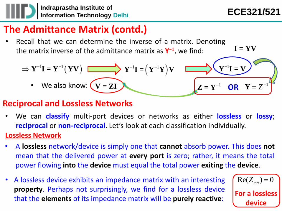
The Admittance Matrix (contd.)• Recall that we can determine the inverse of a matrix. Denoting
the matrix inverse of the admittance matrix as Y−1, we find: I = YV
1 1Y I = Y YV
1 1Y I = Y Y V
1Y I = V
• We also know: V = ZI 1Z = Y
1Y Z OR
Reciprocal and Lossless Networks
• We can classify multi-port devices or networks as either lossless or lossy;reciprocal or non-reciprocal. Let’s look at each classification individually.
Lossless Network
• A lossless network/device is simply one that cannot absorb power. This does notmean that the delivered power at every port is zero; rather, it means the totalpower flowing into the device must equal the total power exiting the device.
• A lossless device exhibits an impedance matrix with an interestingproperty. Perhaps not surprisingly, we find for a lossless devicethat the elements of its impedance matrix will be purely reactive:
Re( ) 0mnZ
For a lossless device

Indraprastha Institute of
Information Technology Delhi ECE321/521
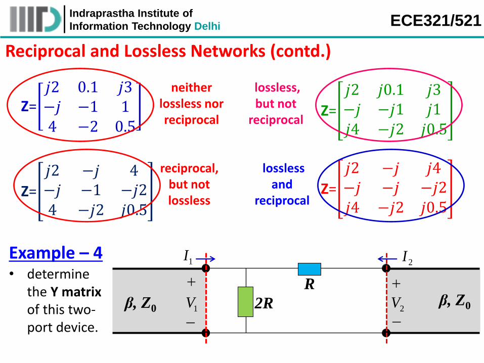
Reciprocal and Lossless Networks
• If the device is lossy, then the elements of the impedance matrix must have atleast one element with a real (i.e., resistive) component.
• Furthermore, we can similarly say that if the elements of an admittance matrix areall purely imaginary (i.e., Re{Ymn} =0), then the device is lossless.
Reciprocal Network
• Ideally, most passive, linear microwave components will turn out to bereciprocal—regardless of whether the designer intended it to be or not!
• Reciprocity is a tremendously important characteristic, as it greatly simplifies animpedance or admittance matrix!
• Specifically, we find that a reciprocal device will result in a symmetric impedanceand admittance matrix, meaning that:
mn nmZ Z For a reciprocal devicemn nmY Y
• For example, we find for a reciprocal device that Z23 =Z32, and Y12 =Y21.
Indraprastha Institute of
Information Technology Delhi ECE321/521
Reciprocal and Lossless Networks (contd.)
Z=𝑗2 0.1 𝑗3−𝑗 −1 14 −2 0.5
Z=
𝑗2 −𝑗 4−𝑗 −1 −𝑗24 −𝑗2 𝑗0.5
Z=
𝑗2 𝑗0.1 𝑗3−𝑗 −𝑗1 𝑗1𝑗4 −𝑗2 𝑗0.5
Z=
𝑗2 −𝑗 𝑗4−𝑗 −𝑗 −𝑗2𝑗4 −𝑗2 𝑗0.5
neither lossless nor reciprocal
lossless, but not
reciprocal
reciprocal, but not lossless
lossless and
reciprocal
β, Z0β, Z0
1V 2V2R
R
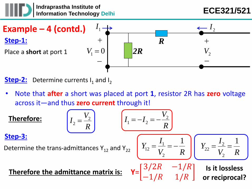
1I 2IExample – 4 • determine
the Y matrix of this two-port device.
Indraprastha Institute of
Information Technology Delhi ECE321/521
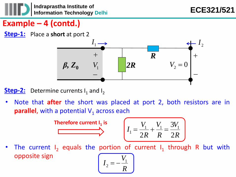
Step-1: Place a short at port 2
β, Z0
1V 2 0V 2R
R
1I 2I
Example – 4 (contd.)
Step-2: Determine currents I1 and I2
• Note that after the short was placed at port 2, both resistors are inparallel, with a potential V1 across each
1 1 11
3
2 2
V V VI
R R R
Therefore current I1 is
• The current I2 equals the portion of current I1 through R but withopposite sign
12
VI
R
Indraprastha Institute of
Information Technology Delhi ECE321/521
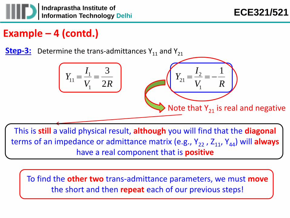
Example – 4 (contd.)
Step-3: Determine the trans-admittances Y11 and Y21
111
1
3
2
IY
V R 2
21
1
1IY
V R
Note that Y21 is real and negative
To find the other two trans-admittance parameters, we must movethe short and then repeat each of our previous steps!
This is still a valid physical result, although you will find that the diagonalterms of an impedance or admittance matrix (e.g., Y22 , Z11, Y44) will always
have a real component that is positive
Indraprastha Institute of
Information Technology Delhi ECE321/521
Example – 4 (contd.)
1 0V 2V2R
R
1I 2I
Step-1:
Place a short at port 1
Step-2: Determine currents I1 and I2
• Note that after a short was placed at port 1, resistor 2R has zero voltageacross it—and thus zero current through it!
Therefore: 22
VI
R
21 2
VI I
R
Step-3:
Determine the trans-admittances Y12 and Y22
112
2
1IY
V R 2
22
2
1IY
V R
Therefore the admittance matrix is: Y=3/2𝑅 −1/𝑅−1/𝑅 1/𝑅
Is it lossless or reciprocal?
Indraprastha Institute of
Information Technology Delhi ECE321/521
Example – 5 𝐼1 𝐼2
𝐼3
1
1
16 𝑉1+
−𝑉2+
−
𝑉3+ −
• Consider this circuit:
• Where the 3-port device ischaracterized by theimpedance matrix:
Z=2 1 21 1 42 4 1
• determine all port voltages V1, V2, V3 and all currents I1, I2, I3.
Indraprastha Institute of
Information Technology Delhi ECE321/521
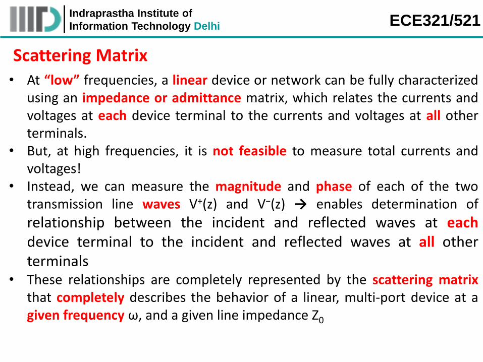
Scattering Matrix
• At “low” frequencies, a linear device or network can be fully characterizedusing an impedance or admittance matrix, which relates the currents andvoltages at each device terminal to the currents and voltages at all otherterminals.
• But, at high frequencies, it is not feasible to measure total currents andvoltages!
• Instead, we can measure the magnitude and phase of each of the twotransmission line waves V+(z) and V−(z) → enables determination of
relationship between the incident and reflected waves at eachdevice terminal to the incident and reflected waves at all otherterminals
• These relationships are completely represented by the scattering matrixthat completely describes the behavior of a linear, multi-port device at agiven frequency ω, and a given line impedance Z0

Indraprastha Institute of
Information Technology Delhi ECE321/521
Scattering Matrix (contd.)
4-port Linear
Microwave Network
1 1( )V z3 3( )V z
2 2( )V z
4 4( )V z
Port-1
Port-4
Port-3
Port-2
3 3Pz z
4 4Pz z
2 2Pz z
1 1Pz z
0Z
0Z0Z
0Z
2 2( )V z
1 1( )V z 3 3( )V z
4 4( )V z
Viewing transmission lineactivity this way, we can fullycharacterize a multi-portdevice by its scatteringparameters!
Note that we have nowcharacterized transmission lineactivity in terms of incident and“reflected” waves. The negativegoing “reflected” waves can beviewed as the waves exiting themulti-port network or device.
Indraprastha Institute of
Information Technology Delhi ECE321/521
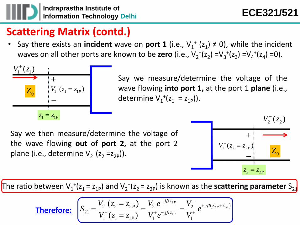
Scattering Matrix (contd.)• Say there exists an incident wave on port 1 (i.e., V1
+ (z1) ≠ 0), while the incidentwaves on all other ports are known to be zero (i.e., V2
+(z2) =V3+(z3) =V4
+(z4) =0).
The ratio between V1+(z1 = z1P) and V2
−(z2 = z2P) is known as the scattering parameter S21
Say we measure/determine the voltage of thewave flowing into port 1, at the port 1 plane (i.e.,determine V1
+(z1 = z1P)).
1 1( )V z
1 1Pz z
1 1 1( )PV z z 0Z
Say we then measure/determine the voltage ofthe wave flowing out of port 2, at the port 2plane (i.e., determine V2
−(z2 =z2P)).
2 2( )V z
2 2Pz z
0Z
2 2 2( )PV z z
Therefore:
2
2 1
1
2 2 2 2 221
1 1 1 1 1
( )
( )
P
P P
P
j zj z zP
j z
P
V z z V e VS e
V z z V e V

Indraprastha Institute of
Information Technology Delhi ECE321/521
Scattering Matrix (contd.)
Similarly: 3 3 331
1 1 1
( )
( )
P
P
V z zS
V z z
4 4 441
1 1 1
( )
( )
P
P
V z zS
V z z
• We of course could also define, say, scattering parameter S34 as the ratiobetween the complex values V3
−(z3 = z3P) (the wave out of port 3) and V4+(z4 = z4P)
(the wave into port 4), given that the input to all other ports (1,2, and 3) are zero
( )
( )
m m mPmn
n n nP
V z zS
V z z
( ) 0k kV z for all k ≠ n
• more generally, the ratio of thewave incident on port n to thewave emerging from port m is:
• Note that, frequently the port positions areassigned a zero value (e.g., z1P=0, z2P=0). Thissimplifies the scattering parameter calculation:
0
0
( 0)
( 0)
j
m m m mmn j
n n n n
V z V e VS
V z V e V
• We will generally assume that the port locations aredefined as znP=0, and thus use the above notation. Butremember where this expression came from!
Indraprastha Institute of
Information Technology Delhi ECE321/521
4-port Linear
Microwave Network
1 1( )V z3 3( )V z
2 2( )V z
4 4( ) 0V z
0Z
0Z0Z
0Z 2 2( ) 0V z
1 1( )V z
3 3( ) 0V z
4 4( )V z
0 30
0 20
0 40
Scattering Matrix (contd.)
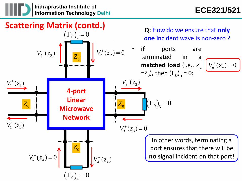
• if ports areterminated in amatched load (i.e., ZL
=Z0), then (Γ0)n = 0:( ) 0n nV z
In other words, terminating a port ensures that there will be no signal incident on that port!
Q: How do we ensure that only one incident wave is non-zero ?
Indraprastha Institute of
Information Technology Delhi ECE321/521
Scattering Matrix (contd.)
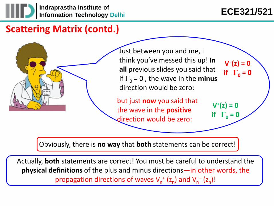
V−(z) = 0 if Γ0 = 0
Just between you and me, I think you’ve messed this up! In all previous slides you said that if Γ0 = 0 , the wave in the minus direction would be zero:
but just now you said that the wave in the positive direction would be zero:
V+(z) = 0 if Γ0 = 0
Obviously, there is no way that both statements can be correct!
Actually, both statements are correct! You must be careful to understand the physical definitions of the plus and minus directions—in other words, the
propagation directions of waves Vn+ (zn) and Vn
− (zn)!
Indraprastha Institute of
Information Technology Delhi ECE321/521
Scattering Matrix (contd.)
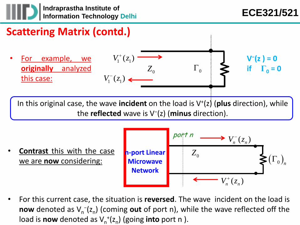
• For example, weoriginally analyzedthis case:
1 1( )V z
1 1( )V z0
V−(z ) = 0 if Γ0 = 0
0Z
• Contrast this with the casewe are now considering:
n-port Linear Microwave
Network
( )n nV z
( )n nV z
0Z 0 n
In this original case, the wave incident on the load is V+(z) (plus direction), while the reflected wave is V−(z) (minus direction).
• For this current case, the situation is reversed. The wave incident on the load isnow denoted as Vn
−(zn) (coming out of port n), while the wave reflected off theload is now denoted as Vn
+(zn) (going into port n ).

Indraprastha Institute of
Information Technology Delhi ECE321/521
Scattering Matrix (contd.)
• back to our discussion of S-parameters. We foundthat if znP = 0 for all ports n, the scatteringparameters could be directly written in terms ofwave amplitudes Vn
+ and Vm−
mmn
n
VS
V
( ) 0k kV z
for all k ≠ n
• Which we can now equivalently state as:
mmn
n
VS
V
(all ports, except port n, are terminated in matched loads)
• One more important note—notice that for the ports terminated in matchedloads (i.e., those ports with no incident wave), the voltage of the exiting wave isalso the total voltage!
( ) 0m m m mj z j z j z j z
m m m m m mV z V e V e V e V e
For all terminated
ports!

Indraprastha Institute of
Information Technology Delhi ECE321/521
Scattering Matrix (contd.) • We can use the scattering matrix to determine the solution for a more general
circuit—one where the ports are not terminated in matched loads!• Since the device is linear, we can apply superposition. The output at any port
due to all the incident waves is simply the coherent sum of the output at thatport due to each wave!
• More generally, the output at port m of an N-port device is:
1
N
m mn n
n
V S V
znP = 0
3 34 4 33 3 32 2 31 1V S V S V S V S V • For example, the output wave at port 3 can
be determined by (assuming znP = 0 ):
• This expression of Scattering parametercan be written in matrix form as:
- +V = SV
- +V = SV
Scattering Matrix
11 12 1
21
1 2
n
m m mn
S S S
S
S S S
S

Indraprastha Institute of
Information Technology Delhi ECE321/521
Scattering Matrix (contd.) • The scattering matrix is N by N matrix that completely characterizes a linear, N-
port device. Effectively, the scattering matrix describes a multi-port device theway that Γ0 describes a single-port device (e.g., a load)!
• The values of the scattering matrix for aparticular device or network, like Γ0, arefrequency dependent! Thus, it may bemore instructive to explicitly write:
11 12 1
21
1 2
( ) ( ) ( )
( )
( ) ( ) ( )
n
m m mn
S S S
S
S S S
S( )
• Also realize that—also just like Γ0—the scattering matrix is dependent on boththe device/network and the Z0 value of the TL connected to it.
• Thus, a device connected to transmission lines with Z0 =50Ω will have acompletely different scattering matrix than that same device connected totransmission lines with Z0 =100Ω
• A device can be lossless or reciprocal. In addition, we can also classify it as beingmatched.
• Let’s examine each of these three characteristics, and how they relate to thescattering matrix.