adcpro(tm) analog-to-digital converter evaluation … · 3.4 evm plug-ins— getting data into...
TRANSCRIPT
ADCPro™
User's Guide
Literature Number: SBAU128C
August 2007–Revised March 2012
Contents
1 Introduction and Requirements ............................................................................................. 41.1 Features .................................................................................................................. 4
1.2 Minimum System Requirements for ADCPro ........................................................................ 5
1.3 Additional Requirements for Use with Hardware .................................................................... 5
1.4 ADCPro Installation ..................................................................................................... 5
2 ADCPro Launcher ............................................................................................................... 52.1 Welcome Tab ............................................................................................................ 6
2.2 General Tab .............................................................................................................. 6
2.3 Updates Tab ............................................................................................................. 7
2.4 Search Tab ............................................................................................................... 7
2.5 Install Tab ................................................................................................................ 8
3 ADCPro .............................................................................................................................. 93.1 Launching ADCPro ...................................................................................................... 9
3.2 ADCPro Architectural Overview ...................................................................................... 10
3.3 ADCPro Main Menus .................................................................................................. 10
3.4 EVM Plug-Ins—Getting Data Into ADCPro ......................................................................... 11
3.5 Test Plug-Ins—Analyzing and Saving Data ........................................................................ 14
3.6 ADCPro Tools .......................................................................................................... 31
4 Troubleshooting ................................................................................................................ 32Appendix A Basics of ADC Measurement and Evaluation ............................................................... 33
A.1 Definitions of Measured Parameters ............................................................................... 33
A.2 Dynamic versus Static Testing ..................................................................................... 42
A.3 Tests and Equipment Requirements ............................................................................... 47
2 Table of Contents SBAU128C–August 2007–Revised March 2012Submit Documentation Feedback
Copyright © 2007–2012, Texas Instruments Incorporated

www.ti.com
List of Figures
1 ADCPro Launcher Enable/Disable Switch............................................................................... 5
2 ADCPro Launcher Welcome Tab ......................................................................................... 6
3 ADCPro Launcher General Tab........................................................................................... 6
4 ADCPro Launcher Updates Tab .......................................................................................... 7
5 ADCPro Launcher New Plug-ins Tab .................................................................................... 8
6 ADCPro Launcher Install Tab ............................................................................................. 8
7 Start-Up Splash Screen .................................................................................................... 9
8 Initial ADCPro Screen ...................................................................................................... 9
9 ADCPro Main Panel with Test Plug-in Maximized .................................................................... 10
10 ADCPro Configuration Settings Menu .................................................................................. 11
11 Selecting an EVM Plug-In ................................................................................................ 11
12 TripleGen EVM Plug-In Front Panel Display........................................................................... 12
13 FileReader Plug-In Front Panel Display ................................................................................ 13
14 Selecting a Test Plug-In .................................................................................................. 14
15 Data Monitor Test Plug-In ................................................................................................ 15
16 MultiScope Plug-In Display............................................................................................... 16
17 Custom Units Control ..................................................................................................... 17
18 Equation Editor Screen ................................................................................................... 17
19 Equation Editor Screen—Example Equation .......................................................................... 18
20 Multiscope Display Screen with Custom Equation .................................................................... 18
21 Graph Controls ............................................................................................................ 19
22 Cursors Display Box ...................................................................................................... 19
23 Noise Histogram Results ................................................................................................. 21
24 Sine Wave Histograms ................................................................................................... 22
25 MultiFFT Test Plug-In ..................................................................................................... 23
26 MultiFFT FFT Tab Controls .............................................................................................. 25
27 MultiFFT Display Tab Controls .......................................................................................... 26
28 Harmonic Markers ......................................................................................................... 26
29 Selecting a File to Record Data ......................................................................................... 27
30 Data Recorder Set Up with File and Length Specified ............................................................... 28
31 Device Name and Notes/Comments for File Dialog .................................................................. 29
32 Coherent Frequency Calculator ......................................................................................... 31
33 ADC Transfer Function ................................................................................................... 33
34 Quantization Error ......................................................................................................... 34
35 Offset Error ................................................................................................................. 35
36 Gain Error .................................................................................................................. 36
37 Differential Nonlinearity (DNL) ........................................................................................... 36
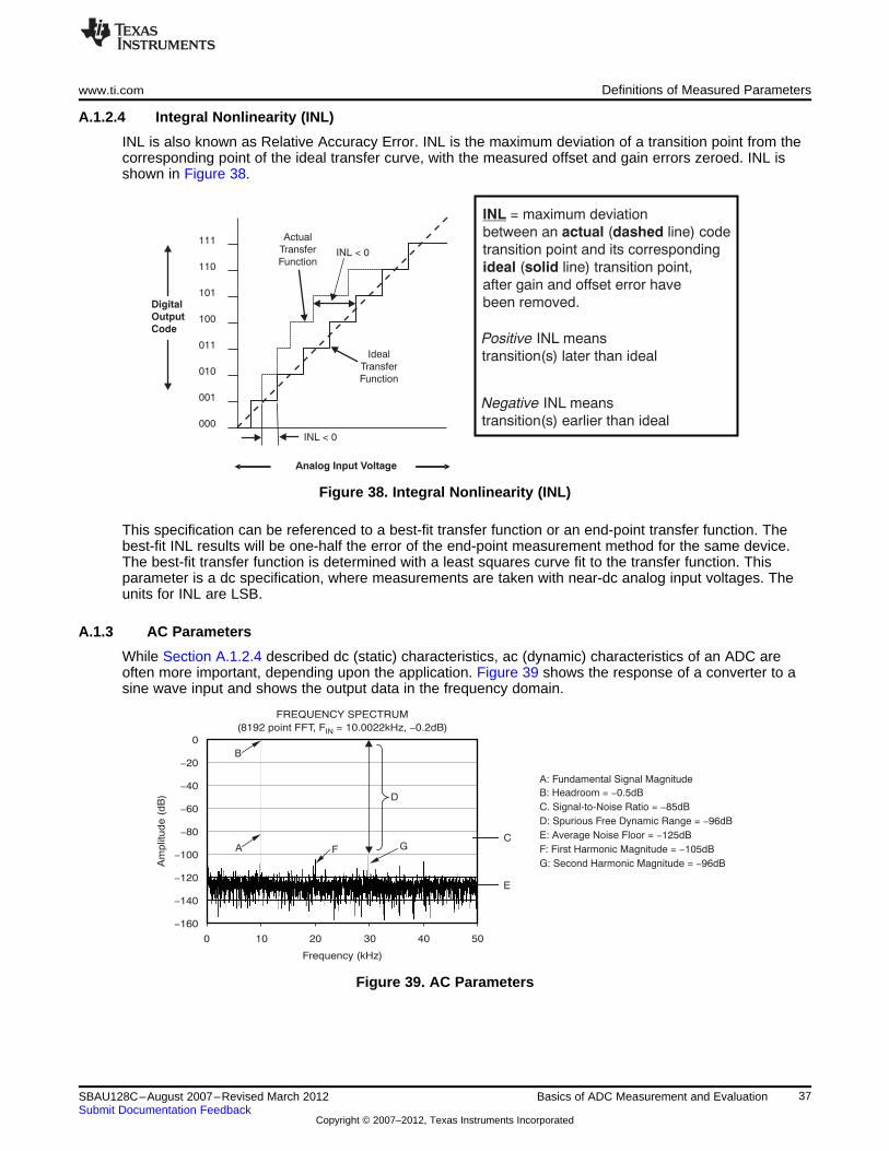
38 Integral Nonlinearity (INL) ................................................................................................ 37
39 AC Parameters ............................................................................................................ 37
40 Spurious-Free Dynamic Range.......................................................................................... 38
41 Fundamental and Harmonic Bins ....................................................................................... 39
42 INL Plot versus Code for 18-Bit ADC ................................................................................... 42
43 Servo-Loop Test Setup ................................................................................................... 43
44 Sine Wave Test Setup .................................................................................................... 44
45 Coherently-Sampled Waveform ......................................................................................... 45
46 Non-Coherently-Sampled Waveform ................................................................................... 46
47 Windowing a Data Record ............................................................................................... 47
3SBAU128C–August 2007–Revised March 2012 List of FiguresSubmit Documentation Feedback
Copyright © 2007–2012, Texas Instruments Incorporated

User's GuideSBAU128C–August 2007–Revised March 2012
ADCPro™ User Guide
This user's guide describes ADCPro™, a software tool for evaluating analog-to-digital converters (ADCs).This tool is provided along with many evaluation modules (EVMs) from Texas Instruments to assistcustomers in evaluating a broad range of ADCs for various applications.
1 Introduction and Requirements
ADCPro is a modular software system from Texas Instruments for evaluating ADCs without the need forexpensive logic analyzers and complex analysis routines. As a stand-alone tool, it is suitable for analyzingdata sets captured during ADC testing. When paired with a Texas Instruments ADC EVM and suitabledata capture card, it becomes part of a powerful evaluation package.
1.1 Features• Ability to save and recall data sets
• Modular design allows additional EVMs and tests to be supported
• Time, histogram, and frequency domain testing
This manual is designed to help easily set up an evaluation system that closely replicates amanufacturer's system, and allows the user to arrive at meaningful results that can be compared tosystem requirements. Tests that are performed and the equipment required to perform these tests will bediscussed; detailed test methodologies are also examined.
In this document, we identify the appropriate test equipment for use with an EVM and review basic ADCevaluation test methods. Essential performance parameters of an ADC are described, as well as howthese parameters are characterized by following the IEEE Standard 1241-2000, the IEEE Standard forTerminology and Test Methods for ADCs. ADCPro implements some of the tests described in IEEE1241-2000. As a result of the modular ADCPro design, additional tests can be added to any installation ofADCPro as needed.
When running the ADCPro, the user is actually using three programs: a shell program that loads plug-ins;a plug-in program that communicates with the EVM hardware; and a test plug-in that analyzes datacoming from the EVM plug-in. This modular design allows ADCPro to be used with a number of differentdata capture cards or motherboards that may ship in an EVM product development kit (PDK). Data filessaved from ADCPro can be recalled for further analysis using an EVM plug-in that reads files.
ADCPro is a trademark of Texas Instruments.Agilent 33120A is a trademark of Agilent Technologies, Inc.Audio Precision is a trademark of Audio Precision, Inc.Pentium III, Celeron are registered trademarks of Intel Inc.Microsoft Windows, Windows are registered trademarks of Microsoft Corp.Microsoft, Excel are registered trademarks of Microsoft Corporation.All other trademarks are the property of their respective owners.
4 ADCPro™ User Guide SBAU128C–August 2007–Revised March 2012Submit Documentation Feedback
Copyright © 2007–2012, Texas Instruments Incorporated

www.ti.com ADCPro Launcher
1.2 Minimum System Requirements for ADCPro• PC with:
– Pentium III®/ Celeron® 866MHz or equivalent processor
– Minimum 256MB of RAM (1GB or greater recommended)
– Hard disk drive with at least 200MB free space
• Microsoft Windows® XP SP2/SP3 and Windows® 7 operating systems
• Mouse
• Optimized for 1024 × 768 resolution
NOTE: Microsoft Windows® 7 includes an option in the Control Panel to scale overall displaymagnification, see Control Panel > Appearance and Personalization > Display. It isrecommended that ADCPro be run on systems with the display magnification set to "Smaller- 100% (Default)" to avoid overlapping text/controls.
1.3 Additional Requirements for Use with Hardware• TI ADC EVM-PDK: evaluation kit that includes data capture card and device EVM (optional)
• USB 1.1-compatible input (check requirements of individual EVMs)
Other configurations may work, but have not been tested. Users should be advised that when capturinglarger data sets, PCs equipped with faster processors and larger RAM tend to perform better.
1.4 ADCPro Installation
For installation instructions please refer to the ADCPro Hardware and Software Installation Manual.
2 ADCPro Launcher
The ADCPro Launcher is a utility provided to ease installation and maintenance of ADCPro. From theLauncher the user may install ADCPro and ADCPro plug-ins, apply updates to ADCPro, visit the TI E2Ecommunity, and search for devices at www.ti.com.
Figure 1. ADCPro Launcher Enable/Disable Switch
The ADCPro Launcher can be enabled or disabled on start-up once ADCPro is installed on the PC. Atcompletion of the ADCPro installation, the prompt shown in Figure 1 will be displayed. The Launcher canalso be enabled or disabled from the ADCPro toolbar under Settings > Configuration Settings - asdiscussed in Section 3.3.
NOTE: No user data outside of the ADCPro and ADCPro plug-in installation is inspected by theADCPro Launcher. No data on the PC is monitored or reported back to Texas Instruments.
5SBAU128C–August 2007–Revised March 2012 ADCPro™ User GuideSubmit Documentation Feedback
Copyright © 2007–2012, Texas Instruments Incorporated

ADCPro Launcher www.ti.com
2.1 Welcome Tab
The Welcome tab is displayed for users who do not have ADCPro installed or for users who are migratingfrom ADCPro v1.2.2 to ADCPro v2.0.0 and beyond. Installed ADCPro plug-ins will be shown on this taband may be selected for update to be compatible with the new version of ADCPro. Click the Get ADCProbutton once all desired components to convert are selected and the Launcher will begin downloading andinstalling the requested features.
Figure 2. ADCPro Launcher Welcome Tab
2.2 General Tab
The General tab is the default window for the ADCPro Launcher. This window will always be the first pagevisible unless ADCPro is not installed on the PC, in this case the Welcome tab is made visible and theuser will be prompted to install ADCPro.
From the General tab the user may check for ADCPro updates, search for new ADCPro plug-ins, visit thePrecision Data Converters E2E Community, search for Precision Data Converter products at www.it.com,and launch ADCPro. Additionally, a message of the day is displayed on this tab to present Precision DataConverter and ADCPro announcements.
NOTE: To Launch ADCPro return to the General tab.
Figure 3. ADCPro Launcher General Tab
6 ADCPro™ User Guide SBAU128C–August 2007–Revised March 2012Submit Documentation Feedback
Copyright © 2007–2012, Texas Instruments Incorporated
www.ti.com ADCPro Launcher
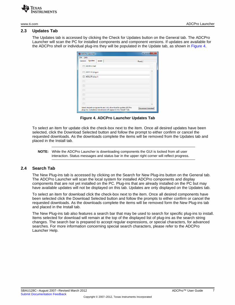
2.3 Updates Tab
The Updates tab is accessed by clicking the Check for Updates button on the General tab. The ADCProLauncher will scan the PC for installed components and component versions. If updates are available forthe ADCPro shell or individual plug-ins they will be populated in the Update tab, as shown in Figure 4.
Figure 4. ADCPro Launcher Updates Tab
To select an item for update click the check-box next to the item. Once all desired updates have beenselected, click the Download Selected button and follow the prompt to either confirm or cancel therequested downloads. As the downloads complete the items will be removed from the Updates tab andplaced in the Install tab.
NOTE: While the ADCPro Launcher is downloading components the GUI is locked from all userinteraction. Status messages and status bar in the upper right corner will reflect progress.
2.4 Search Tab
The New Plug-ins tab is accessed by clicking on the Search for New Plug-ins button on the General tab.The ADCPro Launcher will scan the local system for installed ADCPro components and displaycomponents that are not yet installed on the PC. Plug-ins that are already installed on the PC but mayhave available updates will not be displayed on this tab. Updates are only displayed on the Updates tab.
To select an item for download click the check-box next to the item. Once all desired components havebeen selected click the Download Selected button and follow the prompts to either confirm or cancel therequested downloads. As the downloads complete the items will be removed form the New Plug-ins taband placed in the Install tab.
The New Plug-ins tab also features a search bar that may be used to search for specific plug-ins to install.Items selected for download will remain at the top of the displayed list of plug-ins as the search stringchanges. The search bar is prepared to accept regular expressions, or special characters, for advancedsearches. For more information concerning special search characters, please refer to the ADCProLauncher Help.
7SBAU128C–August 2007–Revised March 2012 ADCPro™ User GuideSubmit Documentation Feedback
Copyright © 2007–2012, Texas Instruments Incorporated

ADCPro Launcher www.ti.com
Figure 5. ADCPro Launcher New Plug-ins Tab
2.5 Install Tab
The Install tab is made visible either by clicking the Install Components button on the General tab or byclicking the Check for Updates or Search for New Plug-ins buttons on the General tab. When downloadsare complete from either the Updates tab or New Plug-ins tab the Install tab will be made visible. TheInstall tab presents all of the components that have been downloaded on the PC. Items can be installedindividually by double-clicking on the item name or all items can be installed automatically by clicking theInstall All button.
NOTE: If an update has been downloaded for the ADCPro shell and components are installedmanually, it is important to run the ADCPro shell installer first, followed by each desiredcomponent. Alternatively, the Install All button will automatically run the shell installer first if itis present.
Figure 6. ADCPro Launcher Install Tab
8 ADCPro™ User Guide SBAU128C–August 2007–Revised March 2012Submit Documentation Feedback
Copyright © 2007–2012, Texas Instruments Incorporated

www.ti.com ADCPro
3 ADCPro
3.1 Launching ADCPro
From the Windows Start menu, select ADCPro....
When ADCPro begins, it displays a splash screen (Figure 7). This screen shows the version number ofthe software. the user can also find the version number under the Help menu.
Figure 7. Start-Up Splash Screen
After a few moments, the software initializes and the splash screen disappears. The screen shown inFigure 8 then displays.
Figure 8. Initial ADCPro Screen
9SBAU128C–August 2007–Revised March 2012 ADCPro™ User GuideSubmit Documentation Feedback
Copyright © 2007–2012, Texas Instruments Incorporated

ADCPro www.ti.com
3.2 ADCPro Architectural Overview
ADCPro is built upon a plug-in architecture using LabVIEW software. The main program, shown inFigure 8, is called the shell. The shell loads plug-ins to collect and analyze data.
Data are collected for analysis using an EVM Plug-In, so named because in most cases the data arecollected from a TI EVM via a hardware interface, usually over a universal serial bus (USB) connection.
When the shell initializes, it scans a directory named evm in the plugins ADCPro directory and populatestwo menus, EVM and Test, with any plug-ins it finds. Plug-ins that provide data to the ADCPro softwareare classified as EVM plug-ins, while those that take the collected data and analyze or manipulate it areclassified as Test plug-ins.
To use ADCPro, the following steps are required:
• Load an EVM plug-in
• Load a Test plug-in
To load an EVM plug-in, select it from the EVM menu. To load a test plug-in, select it from the Test menu.To unload a plug-in, select the Unload option from the respective menu.
Only one of each type of plug-in can be loaded at a time. If selecting a different plug-in, the previous plug-in is automatically unloaded.
3.3 ADCPro Main Menus
The ADCPro shell screen has four drop-down menu options: File, EVM, Test,Tools, Settings, and Help.
• The File menu contains three items: Minimize EVM Plugin, Screen Capture of ADCPro Screen, andExit.
– The Minimize EVM Plugin item collapses the EVM plug-in panel to allow the Test Plug-in to expandto the entire ADCPro main panel. This action can also be performed using the F8 function key.Selecting the menu item again or pressing the function key will restore the main panel to the defaultdisplay.
Figure 9 shows an enlarged view of the Multiscope plug-in panel.
Figure 9. ADCPro Main Panel with Test Plug-in Maximized
10 ADCPro™ User Guide SBAU128C–August 2007–Revised March 2012Submit Documentation Feedback
Copyright © 2007–2012, Texas Instruments Incorporated
www.ti.com ADCPro
– The Screen Capture of ADCPro Screen item allows the user to capture the main panel of ADCProin one of three file formats: jpg, png, or bmp.
– The Exit item closes the ADCPro software when selected. This action can also be performed byusing the Alt+Q key combination.
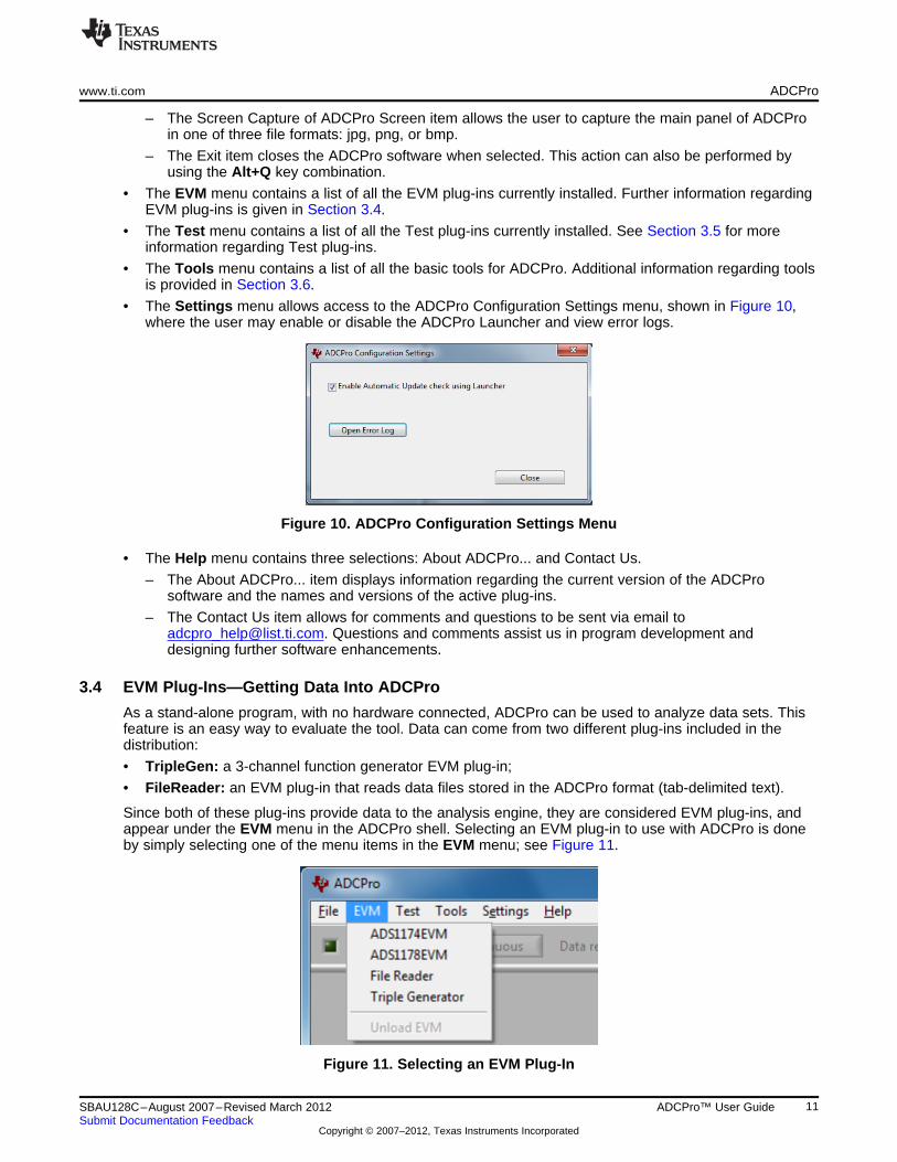
• The EVM menu contains a list of all the EVM plug-ins currently installed. Further information regardingEVM plug-ins is given in Section 3.4.
• The Test menu contains a list of all the Test plug-ins currently installed. See Section 3.5 for moreinformation regarding Test plug-ins.
• The Tools menu contains a list of all the basic tools for ADCPro. Additional information regarding toolsis provided in Section 3.6.
• The Settings menu allows access to the ADCPro Configuration Settings menu, shown in Figure 10,where the user may enable or disable the ADCPro Launcher and view error logs.
Figure 10. ADCPro Configuration Settings Menu
• The Help menu contains three selections: About ADCPro... and Contact Us.
– The About ADCPro... item displays information regarding the current version of the ADCProsoftware and the names and versions of the active plug-ins.
– The Contact Us item allows for comments and questions to be sent via email [email protected]. Questions and comments assist us in program development anddesigning further software enhancements.
3.4 EVM Plug-Ins—Getting Data Into ADCPro
As a stand-alone program, with no hardware connected, ADCPro can be used to analyze data sets. Thisfeature is an easy way to evaluate the tool. Data can come from two different plug-ins included in thedistribution:
• TripleGen: a 3-channel function generator EVM plug-in;
• FileReader: an EVM plug-in that reads data files stored in the ADCPro format (tab-delimited text).
Since both of these plug-ins provide data to the analysis engine, they are considered EVM plug-ins, andappear under the EVM menu in the ADCPro shell. Selecting an EVM plug-in to use with ADCPro is doneby simply selecting one of the menu items in the EVM menu; see Figure 11.
Figure 11. Selecting an EVM Plug-In
11SBAU128C–August 2007–Revised March 2012 ADCPro™ User GuideSubmit Documentation Feedback
Copyright © 2007–2012, Texas Instruments Incorporated
ADCPro www.ti.com
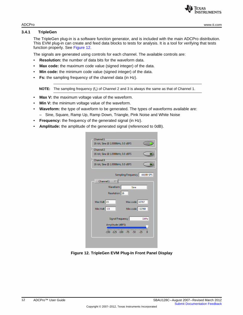
3.4.1 TripleGen
The TripleGen plug-in is a software function generator, and is included with the main ADCPro distribution.This EVM plug-in can create and feed data blocks to tests for analysis. It is a tool for verifying that testsfunction properly. See Figure 12.
The signals are generated using controls for each channel. The available controls are:
• Resolution: the number of data bits for the waveform data.
• Max code: the maximum code value (signed integer) of the data.
• Min code: the minimum code value (signed integer) of the data.
• Fs: the sampling frequency of the channel data (in Hz).
NOTE: The sampling frequency (fS) of Channel 2 and 3 is always the same as that of Channel 1.
• Max V: the maximum voltage value of the waveform.
• Min V: the minimum voltage value of the waveform.
• Waveform: the type of waveform to be generated. The types of waveforms available are:
– Sine, Square, Ramp Up, Ramp Down, Triangle, Pink Noise and White Noise
• Frequency: the frequency of the generated signal (in Hz).
• Amplitude: the amplitude of the generated signal (referenced to 0dB).
Figure 12. TripleGen EVM Plug-In Front Panel Display
12 ADCPro™ User Guide SBAU128C–August 2007–Revised March 2012Submit Documentation Feedback
Copyright © 2007–2012, Texas Instruments Incorporated

www.ti.com ADCPro
3.4.2 FileReader
The FileReader plug-in allows a file that contains a data set to be loaded into the ADCPro shell so that thedata can be analyzed using one of the test plug-ins. It is included with the main ADCPro distribution.
The format of data files that the FileReader can read is described in Section 3.5.5. These files are tab-delimited text files.
The FileReader main panel is shown in Figure 13. To load a file into the FileReader plug-in, select thefolder button to the right of the File Path and Name control. Navigate to the active directory and select thetext file to read. Alternatively, the file path and information can be manually entered into the window. If thefile is a valid file, the LED to the right of the File Path and Name controls should turn green. The headerdata from the file should be displayed in the File Information area of the panel. The CH_Attrib selectorcan be changed to view the individual channel information read from the file.
Figure 13. FileReader Plug-In Front Panel Display
The data in the specified file are read only once at the initial loading of the file. Subsequent acquisitionsperformed by the user do not re-scan the file for any changes and operate from the data stored inmemory. The Rescan button allows the user to rescan the input file without having to reload the file in theFile Path and Name control. This can be useful when reading in a file for analysis that is periodicallyupdating while ADCPro is running.
The channel data contained in the file should be available to read via the Acquire (or the F5 function key)or Continuous function (or the F6 function key) when a Test plug-in is loaded. The channel data are readbeginning at the start of the file, regardless of how many Acquire cycles are issued or the number of datapoints acquired.
13SBAU128C–August 2007–Revised March 2012 ADCPro™ User GuideSubmit Documentation Feedback
Copyright © 2007–2012, Texas Instruments Incorporated

ADCPro www.ti.com
3.4.3 Other EVM Plug-Ins
When physical hardware is available in the form of an EVM-PDK or other evaluation platform, ADCProsupport is provided through the use of an EVM plug-in that comes with its own installer. Running theinstaller places the EVM plug-in into the plug-ins directory of the ADCPro software. EVM plug-insgenerally control any features of the ADC (for example, register settings that control onboard multiplexersor programmable gain amplifiers, as well as parameters such as sample rate). Consult the documentationthat comes with the specific hardware and EVM plug-in for details on using the EVM plug-in with ADCPro.
3.5 Test Plug-Ins—Analyzing and Saving Data
In order for the ADCPro shell to enable the Acquire and Continuous buttons, both an EVM and Testplug-in must be loaded. A test can be selected from the Test menu, as shown in Figure 14.
Figure 14. Selecting a Test Plug-In
ADCPro can perform an analysis in either one-shot or continuous mode. In one-shot mode, the programcollects a number of samples, analyzes them, and stops. In continuous mode, the one-shot operation isperformed repeatedly.
If performing one-shot analysis, all of the samples captured in a block are contiguous. In continuousanalysis, some samples may be missing between blocks.
To perform a one-shot analysis, click the Acquire button (or the F5 function key). To perform continuousanalysis, click the Continuous button (or the F6 function key); to stop continuous analysis, click theContinuous button again.
If no plug-in is ready for analysis, the buttons are disabled.
The number of samples taken depends on the block size set in the test plug-in and/or the number ofpoints set to record in the data recorder.
The maximum block size for any test is 1,048,576 samples per channel.
14 ADCPro™ User Guide SBAU128C–August 2007–Revised March 2012Submit Documentation Feedback
Copyright © 2007–2012, Texas Instruments Incorporated

www.ti.com ADCPro
3.5.1 Data Monitor
The Data Monitor test plug-in allows for the raw data from the ADC to be displayed in the shell. The testdisplays the contents of the channel that is selected from the Channel pull-down button. The channel dataare displayed with the left side of the indicator as a decimal equivalent of the code value and the right sideshowing the channel data as a hexadecimal number equivalent to the code value, as shown in Figure 15.The right hand side display of the data can be modified to display the data in decimal, hexadecimal, octal,binary, or SI notation format by selecting the small gray box located just to the left of the data.
Figure 15. Data Monitor Test Plug-In
15SBAU128C–August 2007–Revised March 2012 ADCPro™ User GuideSubmit Documentation Feedback
Copyright © 2007–2012, Texas Instruments Incorporated
ADCPro www.ti.com
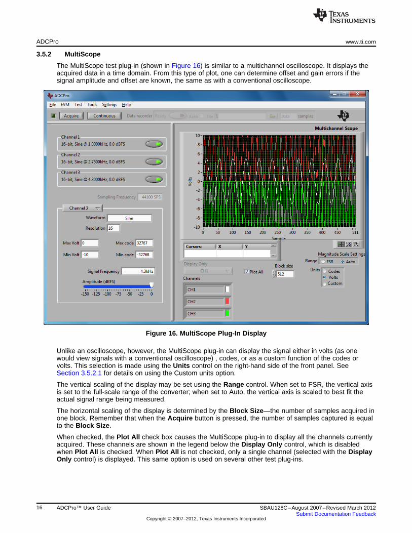
3.5.2 MultiScope
The MultiScope test plug-in (shown in Figure 16) is similar to a multichannel oscilloscope. It displays theacquired data in a time domain. From this type of plot, one can determine offset and gain errors if thesignal amplitude and offset are known, the same as with a conventional oscilloscope.
Figure 16. MultiScope Plug-In Display
Unlike an oscilloscope, however, the MultiScope plug-in can display the signal either in volts (as onewould view signals with a conventional oscilloscope) , codes, or as a custom function of the codes orvolts. This selection is made using the Units control on the right-hand side of the front panel. SeeSection 3.5.2.1 for details on using the Custom units option.
The vertical scaling of the display may be set using the Range control. When set to FSR, the vertical axisis set to the full-scale range of the converter; when set to Auto, the vertical axis is scaled to best fit theactual signal range being measured.
The horizontal scaling of the display is determined by the Block Size—the number of samples acquired inone block. Remember that when the Acquire button is pressed, the number of samples captured is equalto the Block Size.
When checked, the Plot All check box causes the MultiScope plug-in to display all the channels currentlyacquired. These channels are shown in the legend below the Display Only control, which is disabledwhen Plot All is checked. When Plot All is not checked, only a single channel (selected with the DisplayOnly control) is displayed. This same option is used on several other test plug-ins.
16 ADCPro™ User Guide SBAU128C–August 2007–Revised March 2012Submit Documentation Feedback
Copyright © 2007–2012, Texas Instruments Incorporated
www.ti.com ADCPro
3.5.2.1 Custom Units on the Graphic Display
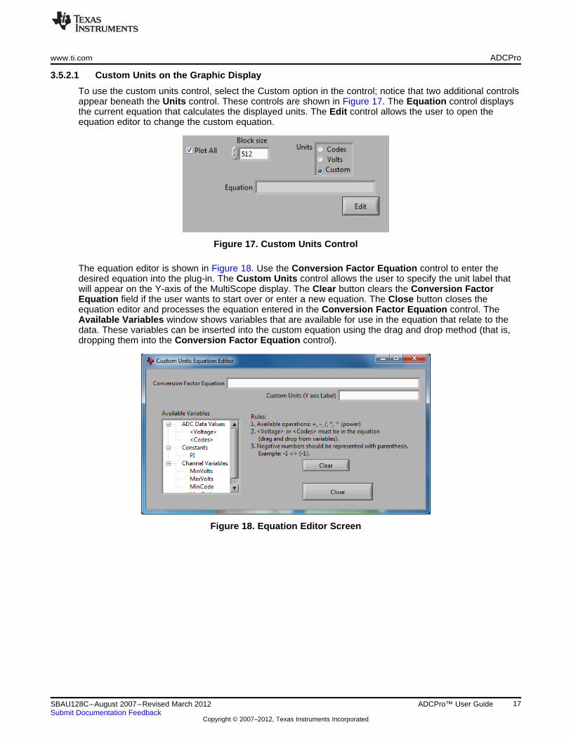
To use the custom units control, select the Custom option in the control; notice that two additional controlsappear beneath the Units control. These controls are shown in Figure 17. The Equation control displaysthe current equation that calculates the displayed units. The Edit control allows the user to open theequation editor to change the custom equation.
Figure 17. Custom Units Control
The equation editor is shown in Figure 18. Use the Conversion Factor Equation control to enter thedesired equation into the plug-in. The Custom Units control allows the user to specify the unit label thatwill appear on the Y-axis of the MultiScope display. The Clear button clears the Conversion FactorEquation field if the user wants to start over or enter a new equation. The Close button closes theequation editor and processes the equation entered in the Conversion Factor Equation control. TheAvailable Variables window shows variables that are available for use in the equation that relate to thedata. These variables can be inserted into the custom equation using the drag and drop method (that is,dropping them into the Conversion Factor Equation control).
Figure 18. Equation Editor Screen
17SBAU128C–August 2007–Revised March 2012 ADCPro™ User GuideSubmit Documentation Feedback
Copyright © 2007–2012, Texas Instruments Incorporated
ADCPro www.ti.com
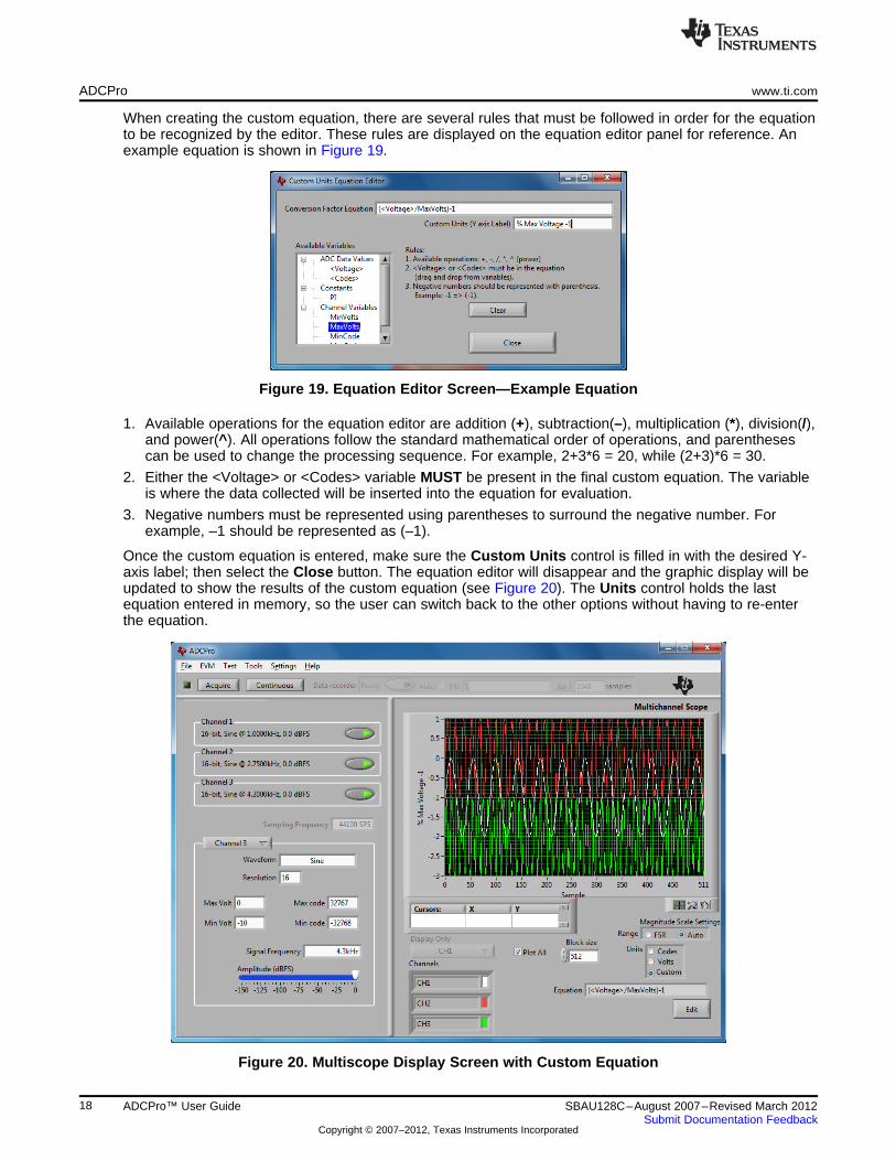
When creating the custom equation, there are several rules that must be followed in order for the equationto be recognized by the editor. These rules are displayed on the equation editor panel for reference. Anexample equation is shown in Figure 19.
Figure 19. Equation Editor Screen—Example Equation
1. Available operations for the equation editor are addition (+), subtraction(–), multiplication (*), division(/),and power(^). All operations follow the standard mathematical order of operations, and parenthesescan be used to change the processing sequence. For example, 2+3*6 = 20, while (2+3)*6 = 30.
2. Either the <Voltage> or <Codes> variable MUST be present in the final custom equation. The variableis where the data collected will be inserted into the equation for evaluation.
3. Negative numbers must be represented using parentheses to surround the negative number. Forexample, –1 should be represented as (–1).
Once the custom equation is entered, make sure the Custom Units control is filled in with the desired Y-axis label; then select the Close button. The equation editor will disappear and the graphic display will beupdated to show the results of the custom equation (see Figure 20). The Units control holds the lastequation entered in memory, so the user can switch back to the other options without having to re-enterthe equation.
Figure 20. Multiscope Display Screen with Custom Equation
18 ADCPro™ User Guide SBAU128C–August 2007–Revised March 2012Submit Documentation Feedback
Copyright © 2007–2012, Texas Instruments Incorporated
www.ti.com ADCPro
3.5.2.2 MultiScope Graphic Display Options
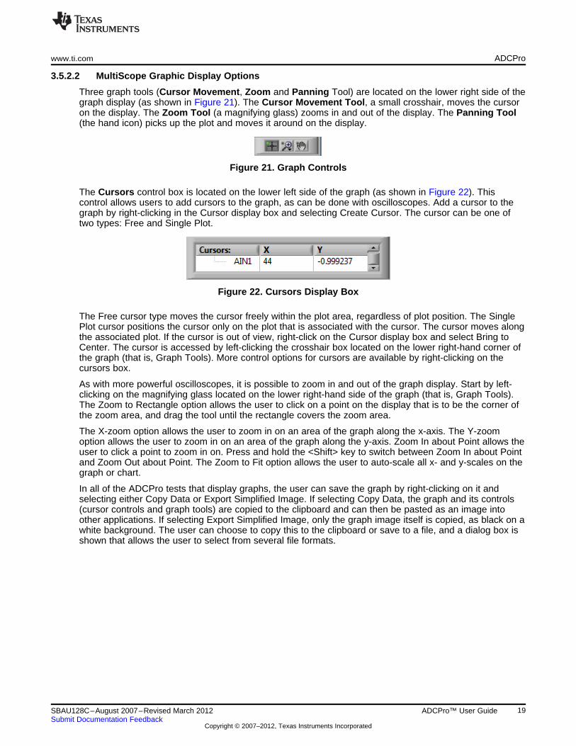
Three graph tools (Cursor Movement, Zoom and Panning Tool) are located on the lower right side of thegraph display (as shown in Figure 21). The Cursor Movement Tool, a small crosshair, moves the cursoron the display. The Zoom Tool (a magnifying glass) zooms in and out of the display. The Panning Tool(the hand icon) picks up the plot and moves it around on the display.
Figure 21. Graph Controls
The Cursors control box is located on the lower left side of the graph (as shown in Figure 22). Thiscontrol allows users to add cursors to the graph, as can be done with oscilloscopes. Add a cursor to thegraph by right-clicking in the Cursor display box and selecting Create Cursor. The cursor can be one oftwo types: Free and Single Plot.
Figure 22. Cursors Display Box
The Free cursor type moves the cursor freely within the plot area, regardless of plot position. The SinglePlot cursor positions the cursor only on the plot that is associated with the cursor. The cursor moves alongthe associated plot. If the cursor is out of view, right-click on the Cursor display box and select Bring toCenter. The cursor is accessed by left-clicking the crosshair box located on the lower right-hand corner ofthe graph (that is, Graph Tools). More control options for cursors are available by right-clicking on thecursors box.
As with more powerful oscilloscopes, it is possible to zoom in and out of the graph display. Start by left-clicking on the magnifying glass located on the lower right-hand side of the graph (that is, Graph Tools).The Zoom to Rectangle option allows the user to click on a point on the display that is to be the corner ofthe zoom area, and drag the tool until the rectangle covers the zoom area.
The X-zoom option allows the user to zoom in on an area of the graph along the x-axis. The Y-zoomoption allows the user to zoom in on an area of the graph along the y-axis. Zoom In about Point allows theuser to click a point to zoom in on. Press and hold the <Shift> key to switch between Zoom In about Pointand Zoom Out about Point. The Zoom to Fit option allows the user to auto-scale all x- and y-scales on thegraph or chart.
In all of the ADCPro tests that display graphs, the user can save the graph by right-clicking on it andselecting either Copy Data or Export Simplified Image. If selecting Copy Data, the graph and its controls(cursor controls and graph tools) are copied to the clipboard and can then be pasted as an image intoother applications. If selecting Export Simplified Image, only the graph image itself is copied, as black on awhite background. The user can choose to copy this to the clipboard or save to a file, and a dialog box isshown that allows the user to select from several file formats.
19SBAU128C–August 2007–Revised March 2012 ADCPro™ User GuideSubmit Documentation Feedback
Copyright © 2007–2012, Texas Instruments Incorporated
ADCPro www.ti.com
3.5.3 MultiHisto
Histogram testing is used extensively in characterizing ADCs. A histogram is merely a count of thenumber of times a code has occurred in a particular data set. The MultiHisto test plug-in creates ahistogram of the data in the acquired data set and displays it. This feature can be useful in two distinctways: noise testing and linearity testing.
Noise is the uncertainty of a measurement. With earlier-generation 8-bit and 12-bit converter ICs, notmuch attention was usually given to this important aspect of electronic measurement because it is notdifficult to make an 8-bit or 12-bit converter relatively noise-free.
Low-noise, delta-sigma (ΔΣ) converters have brought this topic to the attention of many designers. 24-bit,noise-free resolution is an extraordinarily difficult thing to obtain. Therefore, we need a way to measureand evaluate noise.
In many ac measurement applications, such as audio and radio circuits, noise measurement techniquesare well-known. Typically, noise measurements are obtained by analyzing the measured signal in thefrequency domain. A Fast Fourier Transform (FFT) plot taken of a high-speed converter output provides auseful estimate of the device noisiness. The figure measured here is called signal-to-noise ratio.
In low-frequency measurement applications, however, an FFT plot is not nearly as useful because we aremeasuring signals near dc. Instead, we want to measure how certain we are of the value reported by theconverter. We obtain this by making many successive conversions with a single dc input applied to theconverter and calculating statistical functions over the collected data.
The two most common measurements of certainty for an ADC are RMS noise and peak-to-peak noise.RMS noise is more applicable to an ADC, since it does not depend on the kind of noise present. Peak-to-peak noise calculations, however, are not as mathematically rigorous, and often assume that the noise isGaussian in distribution, but they are essential for applications (such as weigh scales and thermometers)where the flicker or constancy of a displayed value must be known.
Ideally, a fixed dc input to an ADC should result in the same output code for every conversion. Even witha precision ADC, for a given input voltage the user should expect to see a range of output codes. Thisresult is caused by circuit noise within the ADC. The noise is equivalent to summing the broadband noisewith the input of a noiseless ADC.
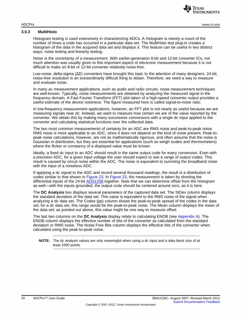
If applying a dc signal to the ADC and record several thousand readings, the result is a distribution ofcodes similar to that shown in Figure 23. In Figure 23, the measurement is taken by shorting thedifferential inputs of the 24-bit ADS1258 together. Note that we can determine offset from the histogramas well—with the inputs grounded, the output code should be centered around zero, as it is here.
The DC Analysis box displays several parameters of the captured data set. The StDev column displaysthe standard deviation of the data set. This value is equivalent to the RMS noise of the signal whenanalyzing a dc data set. The Codes (pp) column shows the peak-to-peak spread of the codes in the dataset; for a dc data set, this range would be the peak-to-peak noise. The Mean column displays the mean ofthe data set; as pointed out above, this value might be one way to measure offset.
The last two columns on the DC Analysis display relate to calculating ENOB (see Appendix A). TheENOB column displays the effective number of bits of the converter as calculated from the standarddeviation or RMS noise. The Noise Free Bits column displays the effective bits of the converter whencalculated using the peak-to-peak noise.
NOTE: The dc analysis values are only meaningful when using a dc input and a data block size of atleast 1000 points.
20 ADCPro™ User Guide SBAU128C–August 2007–Revised March 2012Submit Documentation Feedback
Copyright © 2007–2012, Texas Instruments Incorporated
www.ti.com ADCPro
Figure 23. Noise Histogram Results
Histograms can be taken on any number of dynamic signals. Ramp signals or sine waves are the mostcommonly-used signals. Histograms are taken of these signals to determine linearity. A ramp input shouldexercise every code in the transfer function as it ramps from one end of the converter range to the other.This measurement should result in a flat histogram; variations from this ideal reveal shorter or longercodes. As the converter resolution increases, the required linearity of the ramp input signal becomesdifficult to create with common test equipment. This difficulty is why a sine wave input is often used,because it is easier to create a highly accurate sine wave by filtering a high-quality signal generator. Theshape of a sine wave histogram is the probability density function for a sine wave. Figure 24 shows threechannels of sine wave data and the resulting respective histograms.
21SBAU128C–August 2007–Revised March 2012 ADCPro™ User GuideSubmit Documentation Feedback
Copyright © 2007–2012, Texas Instruments Incorporated

ADCPro www.ti.com
Figure 24. Sine Wave Histograms
By comparing the measured sine wave histogram to the ideal probability density function (PDF) for a sinewave, one can determine both integral nonlinearity (INL) and differential nonlinearity (DNL) errors. In boththe ramp and sine wave methods, several hits per code (~50 or more) are required for meaningful results.This condition means that a proper measurement requires a very large data set for higher resolutionconverters—for example, a 16-bit converter requires a data set of approximately four million samples. TheMultiHisto plug-in does not at this time calculate INL or DNL data.
The Codes/bin control affects the qualitative look of the histogram display. For the highest accuracy ofreading the display, this control should be set to one code per bin. However, it can be set to a highernumber to make it easier to see some qualitative features of the histogram. For example, in Figure 24, thiscontrol is set to 500, combining 500 codes into one bin. Having collected only 8192 points, a one code/bindisplay would not look like the sine wave in this example; by setting this limit higher, we can see thecharacteristic sine wave PDF and observe that the input was a sine wave.
The To File >> control allows the histogram data to be saved in a tab-delimited text file format that can beimported into Microsoft® Excel®or other spreadsheet/software tools. This file contains the processedhistogram data, not the raw data, which is available via the DataRecorder plug-in. The DC Analysisstatistics are also included at the beginning of the file for reference.
22 ADCPro™ User Guide SBAU128C–August 2007–Revised March 2012Submit Documentation Feedback
Copyright © 2007–2012, Texas Instruments Incorporated

www.ti.com ADCPro
3.5.4 MultiFFT
The MultiFFT test plug-in performs a Fast Fourier Transform (FFT) computation on a record of data, anddisplays the resulting frequency domain plot on its main graph. It also calculates key performanceparameters such as SNR, THD, SINAD (that is, THD + noise), and SFDR (for definitions of theseparameters, see Appendix A). Figure 25 shows the MultiFFT display. Some distortion components and themeasurements of the calculated parameters are available in the box near the bottom of the MultiFFTwindow.
Figure 25. MultiFFT Test Plug-In
The ideal sine wave test setup for performing FFT tests includes a sine wave generator that can bephase-locked to the sample clock. In cases where this coherent sampling can be done, no windowing ofthe data is necessary; with converter systems where phase locking to the clock is impractical, windowingfunctionality is usually used. See Appendix A for details on coherent sampling and windowing.
The To File >> control allows the FFT data to be saved in a tab-delimited text file format that can beimported into Excel or other spreadsheet/software tools. This file contains the processed FFT data, not theraw data, which is available via the DataRecorder plug-in. The AC Analysis statistics are also included atthe beginning of the file for reference.
The FFT display has several controls that allow users to manipulate the data and provide detailedinformation gathering. These features include:
• Harmonic Cursors
• Frequency and Amplitude Scaling
• Graph Controls
• Window Function
23SBAU128C–August 2007–Revised March 2012 ADCPro™ User GuideSubmit Documentation Feedback
Copyright © 2007–2012, Texas Instruments Incorporated

ADCPro www.ti.com
• Display Only and Plot All
• Block Size
• Leakage bins controls for DC, Fundamental, and Harmonic Frequencies
In addition to the controls, displays also provide statistical data and other information from the collecteddata.
3.5.4.1 Main Panel Graph Controls
The display also features graph controls and cursors. See Section 3.5.2 for more information about usingthese controls.
Display Only and Plot All
The display provides the ability to plot multiple channels or only one channel at a time. This functionbehaves the same as described in Section 3.5.2.
Block Size
In order to provide accurate FFT analysis, the number of data points is typically restricted to 2n, where n isan integer. The Block Size control provides a drop-down list for values that satisfy this requirement.
3.5.4.2 MultiFFT Tab Graph Controls
The MultiFFT plug-in has three tabs located at the bottom of the panel: Stats, FFT, and Display.Figure 25, Figure 26, and Figure 27 show the different views of each tab.
The Stats Tab is displayed as the default and shows the channel legend and the calculated statistical datafrom the data collected. The FFT Tab contains controls that allow for the customization of the FFT displayand calculated statistical data.
3.5.4.2.1 Stats Tab Controls
The AC Analysis box displays several parameters of the captured data set. In all but the Signal Powerdisplay, these parameters are displayed in terms of dBc, or decibels to carrier—in other words, referencedto the power of the input signal. The actual input Signal Power is displayed in terms of dBFS, that is,referenced to the full-scale range of the converter. See Figure 25 for a screenshot of the Stats tab.
• The SNR column displays the signal-to-noise ratio of the data set. See Appendix A for moreinformation.
• The THD column shows the total harmonic distortion in the data set. See Appendix A for moreinformation.
• The SINAD column displays the value of the signal to noise + distortion ratio. See Appendix A for moreinformation.
• The Tone, Hz column shows the frequency of the largest amplitude signal (in hertz), typically thefundamental frequency.
• The SFDR column displays the spurious-free dynamic range of the data set. See Appendix A for moreinformation.
• The Signal Power(dB) column displays the signal magnitude of the frequency in Tone, Hz.
3.5.4.2.2 FFT Tab Controls
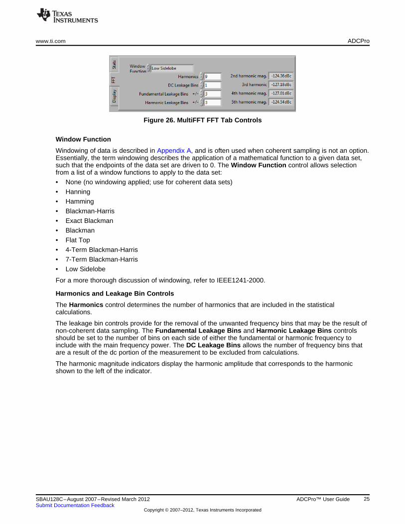
Controls for windowing and leakage bins allow control over how the FFT is processed, and displays areprovided for the harmonic frequency magnitudes. The FFT Tab is shown in Figure 26.
24 ADCPro™ User Guide SBAU128C–August 2007–Revised March 2012Submit Documentation Feedback
Copyright © 2007–2012, Texas Instruments Incorporated
www.ti.com ADCPro
Figure 26. MultiFFT FFT Tab Controls
Window Function
Windowing of data is described in Appendix A, and is often used when coherent sampling is not an option.Essentially, the term windowing describes the application of a mathematical function to a given data set,such that the endpoints of the data set are driven to 0. The Window Function control allows selectionfrom a list of a window functions to apply to the data set:
• None (no windowing applied; use for coherent data sets)
• Hanning
• Hamming
• Blackman-Harris
• Exact Blackman
• Blackman
• Flat Top
• 4-Term Blackman-Harris
• 7-Term Blackman-Harris
• Low Sidelobe
For a more thorough discussion of windowing, refer to IEEE1241-2000.
Harmonics and Leakage Bin Controls
The Harmonics control determines the number of harmonics that are included in the statisticalcalculations.
The leakage bin controls provide for the removal of the unwanted frequency bins that may be the result ofnon-coherent data sampling. The Fundamental Leakage Bins and Harmonic Leakage Bins controlsshould be set to the number of bins on each side of either the fundamental or harmonic frequency toinclude with the main frequency power. The DC Leakage Bins allows the number of frequency bins thatare a result of the dc portion of the measurement to be excluded from calculations.
The harmonic magnitude indicators display the harmonic amplitude that corresponds to the harmonicshown to the left of the indicator.
25SBAU128C–August 2007–Revised March 2012 ADCPro™ User GuideSubmit Documentation Feedback
Copyright © 2007–2012, Texas Instruments Incorporated
ADCPro www.ti.com
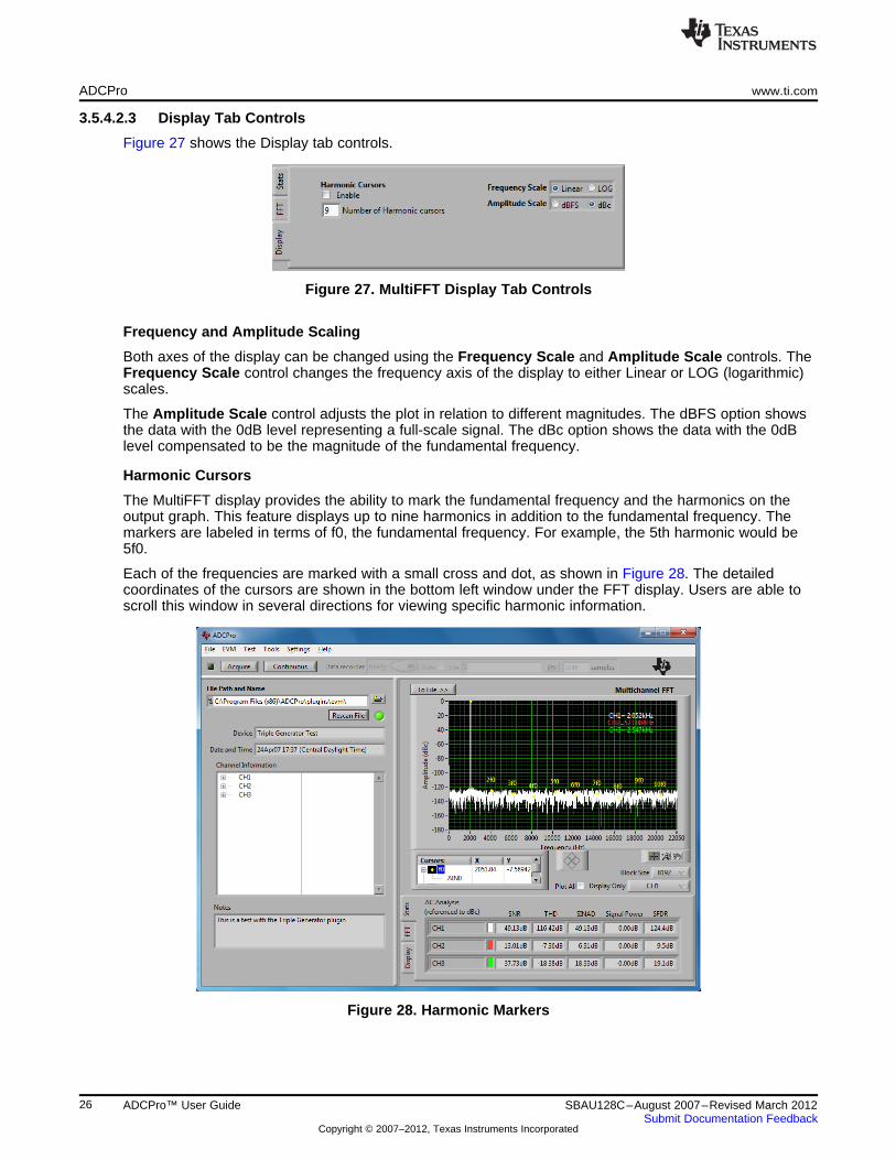
3.5.4.2.3 Display Tab Controls
Figure 27 shows the Display tab controls.
Figure 27. MultiFFT Display Tab Controls
Frequency and Amplitude Scaling
Both axes of the display can be changed using the Frequency Scale and Amplitude Scale controls. TheFrequency Scale control changes the frequency axis of the display to either Linear or LOG (logarithmic)scales.
The Amplitude Scale control adjusts the plot in relation to different magnitudes. The dBFS option showsthe data with the 0dB level representing a full-scale signal. The dBc option shows the data with the 0dBlevel compensated to be the magnitude of the fundamental frequency.
Harmonic Cursors
The MultiFFT display provides the ability to mark the fundamental frequency and the harmonics on theoutput graph. This feature displays up to nine harmonics in addition to the fundamental frequency. Themarkers are labeled in terms of f0, the fundamental frequency. For example, the 5th harmonic would be5f0.
Each of the frequencies are marked with a small cross and dot, as shown in Figure 28. The detailedcoordinates of the cursors are shown in the bottom left window under the FFT display. Users are able toscroll this window in several directions for viewing specific harmonic information.
Figure 28. Harmonic Markers
26 ADCPro™ User Guide SBAU128C–August 2007–Revised March 2012Submit Documentation Feedback
Copyright © 2007–2012, Texas Instruments Incorporated

www.ti.com ADCPro
In order to add the harmonic cursors, do the following:
1. Deselect the Plot All option beside the Display Only control. The cursors can only be displayed forone channel at a time. Deselecting Plot All should enable the Harmonics selection box and numbercontrol.
2. Choose the number of harmonics to display by entering the number in the Harmonics number control.The default setting shows nine harmonics.
3. Check the Harmonics selection box; the harmonic cursors should be added to the FFT display.
The number of harmonics can be changed and the display should update. Selecting the Plot All feature ordisabling the Harmonics selection box removes the harmonic cursors from the FFT display.
3.5.5 Data Recorder
The Data Recorder saves acquired data samples to a file. The user does not need to load a specific testplug-in to use the Data Recorder. If a test plug-in is loaded, it analyzes samples as they are recorded.
Follow this procedure to record samples:
1. Click the small folder icon in the Data Recorder. A file dialog box opens, as displayed in Figure 29.
2. Enter the name of a file, or select a file to record to. ADCPro data files are saved as ASCII (tab-delimited) text files, so a .txt extension is the appropriate file extension to use.
Figure 29. Selecting a File to Record Data
27SBAU128C–August 2007–Revised March 2012 ADCPro™ User GuideSubmit Documentation Feedback
Copyright © 2007–2012, Texas Instruments Incorporated

ADCPro www.ti.com
3. The file path appears in the File box.
4. Select a number of samples to record by putting a number in the Length control. Note that Lengthdoes not have to be the same size as a loaded test block size. Figure 30 shows the Data Recorderwith file and length values specified.
Figure 30. Data Recorder Set Up with File and Length Specified
28 ADCPro™ User Guide SBAU128C–August 2007–Revised March 2012Submit Documentation Feedback
Copyright © 2007–2012, Texas Instruments Incorporated
www.ti.com ADCPro
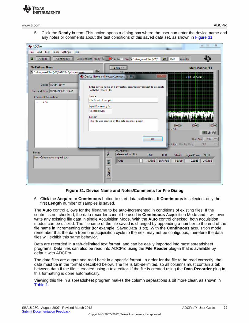
5. Click the Ready button. This action opens a dialog box where the user can enter the device name andany notes or comments about the test conditions of this saved data set, as shown in Figure 31.
Figure 31. Device Name and Notes/Comments for File Dialog
6. Click the Acquire or Continuous button to start data collection. If Continuous is selected, only thefirst Length number of samples is saved.
The Auto control allows for the filename to be auto-incremented in conditions of existing files. If thecontrol is not checked, the data recorder cannot be used in Continuous Acquisition Mode and it will over-write any existing file data in single Acquisition Mode. With the Auto control checked, both acquisitionmodes can be utilized. The filename of the file saved is changed by appending a number to the end of thefile name in incrementing order (for example, SavedData_1.txt). With the Continuous acquisition mode,remember that the data from one acquisition cycle to the next may not be contiguous, therefore the datafiles will exhibit this same behavior.
Data are recorded in a tab-delimited text format, and can be easily imported into most spreadsheetprograms. Data files can also be read into ADCPro using the File Reader plug-in that is available bydefault with ADCPro.
The data files are output and read back in a specific format. In order for the file to be read correctly, thedata must be in the format described below. The file is tab-delimited, so all columns must contain a tabbetween data if the file is created using a text editor. If the file is created using the Data Recorder plug-in,this formatting is done automatically.
Viewing this file in a spreadsheet program makes the column separations a bit more clear, as shown inTable 1.
29SBAU128C–August 2007–Revised March 2012 ADCPro™ User GuideSubmit Documentation Feedback
Copyright © 2007–2012, Texas Instruments Incorporated

ADCPro www.ti.com
Table 1. Sample Tab-Delimited Text File
[Device Information]
EVM Device Name Triple Gen
Date and Time 4/24/2007 5:21:58 PM
Notes This is a test with Triple Gen
Number of Channels 3
blank
[Channel Information]
Channel Name CH1 CH2 CH3
Sampling Frequency 44100.000 44100.000 44100.000
Input Frequency 1001 1002 1003
Max Code 32767 32767 32767
Max Voltage 0.000 15.000 5.000
Min Code –32768 –32768 –32768
Min Voltage –15.000 0.000 –5.000
Data Format Decimal Decimal Decimal
blank
[Channel Data]
32767 –7450 14820
32767 –9979 10563
32767 –12444 6306
32767 –14829 2050
–32768 –17119 –2207
The first four rows contain the following information.
• EVM Device Name: Text describing the device used. The Data Recorder plug-in prompts the user forthis information.
• Date and Time: Date and time the file was created.
• Notes: Notes for this test (the Data Recorder plug-in).
• Number of Channels: Number of data channels in this file.
A blank row is then inserted, followed by a row with the entry [Channel Information]. This row denotesthe start of the Channel Information section. This section includes this information:
• Channel Name: Name of each channel of data.
• Sampling Frequency: Sampling frequency for each channel of data.
• Input Frequency: Main input frequency for each channel of data.
• Max Code: Maximum code value for each channel of data.
• Max Voltage: Maximum voltage for each channel of data.
• Min Code: Minimum code value for each channel of data.
• Min Voltage: Minimum voltage for each channel of data.
• Data Format: The data format for each channel, either Hexadecimal or Decimal.
Another blank row follows this field, followed by a row with the entry [Channel Data]. This row denotesthe start of the data section. The actual data are formatted in columns with tabs separating each column.Note that there is an extra tab at the beginning of the line, making the first column of data actually start inthe second column.
30 ADCPro™ User Guide SBAU128C–August 2007–Revised March 2012Submit Documentation Feedback
Copyright © 2007–2012, Texas Instruments Incorporated

www.ti.com ADCPro
3.6 ADCPro Tools
ADCPro tools are applications designed to aid converter testing with ADCPro.
Presently, the only available tool is the Coherent Frequency Calculator (see Figure 32). This is a tool thatcan help find the best input frequency to use for a given sample rate, in order to do coherent sampling(see Appendix A). Even if the user cannot phase-lock the source to the sampling clock, by using the rightinput frequency one can often eliminate the need to window data for FFT testing (see Appendix A fordetails).
Figure 32. Coherent Frequency Calculator
Follow these Instructions to use the Coherent Frequency Calculator.
1. Enter the sampling frequency in the Sampling Frequency box.
2. In the Input Frequency box, enter the desired input frequency to be tested.
3. Enter the Desired Record Length by clicking on the box and selecting an option from the drop-downmenu. This value should match the Block Size of the test (usually an FFT) being performed.
The Prime Coherent Frequencies table displays the frequencies that would provide a coherent data setgiven the input conditions. In the example shown in Figure 32, a 1000Hz frequency is desired, but a1022.338867Hz input would be coherent. It is usually best to choose a frequency that provides a primenumber of cycles—in this example, 67 cycles would be a better choice than 69 (because 69 is divisible by3, it is not a prime number).
When the user is done using the calculator, press the Close button and the calculator window closes.
31SBAU128C–August 2007–Revised March 2012 ADCPro™ User GuideSubmit Documentation Feedback
Copyright © 2007–2012, Texas Instruments Incorporated

Troubleshooting www.ti.com
4 Troubleshooting
Problem: ADCPro is not responding.
Solution: If ADCPro stops responding while an EVM-PDK is connected, try unplugging the power supplyfrom the EVM-PDK. Unload and reload the EVM plug-in before reapplying power to the PDK.
Problem: On large data captures, it takes a long time to update the graph.
Solution: Performance depends heavily on the computer memory available. For normal sinusoidal ADCanalysis, it is advisable to use 16k or 32k points.
Problem: ADCPro error state memory is full for the histogram or FFT plug-ins.
Solution: For MultiHisto and MultiFFT, the data processing has a large memory requirement.Processing large data sizes for the FFT or large data ranges and small codes/bin values may causememory limitations based on the user's computer memory resources. For the histogram, increasing thecodes/bin value can help alleviate this error.
If the plug-in loads in the panel and cannot connect to the hardware, try resetting the hardware bypressing the Reset button on the motherboard. The plug-in should then be unloaded and reloaded. Theplug-in should now proceed through the firmware download and connection.
Problem: ADCPro times out when loading my software for the first time.
Solution: ADCPro has a built-in timeout function when loading the firmware. Therefore, the software maytimeout when the drivers are loaded during the first run after software installation. Unload the plug-in, resetthe motherboard by pressing the Reset button, and reload the plug-in. The plug-in should load thefirmware and connect normally.
32 ADCPro™ User Guide SBAU128C–August 2007–Revised March 2012Submit Documentation Feedback
Copyright © 2007–2012, Texas Instruments Incorporated

000
Analog Input Voltage
001
010
011
100
101
110
111
Digital
Output
Code
FS1/2 FS 3/4 FS1/4 FS0
Transition point = where
output code changes
from one code
to an adjacent code
Ideal transfer function
for a 3-bit A/D
Transition
Points
code widthIdeal code width =
1LSB
www.ti.com
Appendix A Basics of ADC Measurement and Evaluation
The information presented in this section is relevant for all ADC evaluation and performancecharacterization. For further information, please refer to the IEEE Standard 1241-2000.
NOTE: For additional examples and explanations of these measured parameters, users areencouraged to download and review a copy of Texas Instruments' application reportSBAA147, A Glossary of Analog-to-Digital Specifications and Performance Characteristics.
A.1 Definitions of Measured Parameters
One primary task in evaluating an ADC is determining its transfer function. Ideally, a converter would havea transfer function similar to that shown in Figure 33. This graph shows a transfer function for a 3-bitconverter. Ideally, the width of each code is exactly the same, and a straight line can be drawn throughthe midpoints of each code plateau. In practice, this performance is not always observed; determining thetransition points and code widths is critical to ADC testing and characterization, because it lets us seewhere the actual transfer function deviates from the ideal.
Figure 33. ADC Transfer Function
33SBAU128C–August 2007–Revised March 2012 Basics of ADC Measurement and EvaluationSubmit Documentation Feedback
Copyright © 2007–2012, Texas Instruments Incorporated

Ideal Straight Line
Center
Digital Output
Code
0...101
0...100
0...011
0...010
0...001
0...000
0 1 5432
+1/2 LSB
-1/2 LSB
0 1 5432
Step Width (1LSB)
Analog Input
Value
Midstep Value
of 0...011
Quantization
Error
Analog Input
Value
Inherent Quantization Error ( 1/2 LSB)±
Definitions of Measured Parameters www.ti.com
A.1.1 Quantization Noise
Because the converter can only represent certain values, it deviates from the ideal straight line; thedeviation occurs in a repeatable pattern. The error varies by ±0.5 LSB, as shown in Figure 34. This erroris known as quantization error or quantization noise.
Figure 34. Quantization Error
Why would the quantization error be considered noise? If a signal varies across the full-input range, thenthis error signal is present as well; and anything that is not signal in the transmitted code is, by definition,noise. Thus, this error is correctly identified as quantization noise.
34 Basics of ADC Measurement and Evaluation SBAU128C–August 2007–Revised March 2012Submit Documentation Feedback
Copyright © 2007–2012, Texas Instruments Incorporated
Actual
Transfer
Function
Ideal
Transfer
Function
Offset Error
Offset errors can be
corrected in software or
hardware.
000
Analog Input Voltage
001
010
011
100
101
110
111
Digital
Output
Code
FS1/2 FS 3/4 FS1/4 FS0
Offset Error = Difference
between the actual ( line)
first transition point and the
ideal ( line) first transition point.
dashed
solidFirst (Ideal)
Code
Transition
Offset Error = (V[0:1] 0.5V )- 1LSB
V =1LSB = Ideal LSB Voltage SizeVREF
2n
www.ti.com Definitions of Measured Parameters
A.1.2 DC Parameters
The parameters described in this section are primarily tested at dc. See Section A.2 for a description ofcommon test setups used for these parameters.
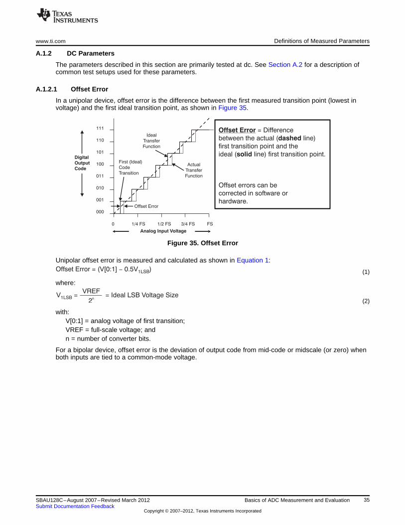
A.1.2.1 Offset Error
In a unipolar device, offset error is the difference between the first measured transition point (lowest involtage) and the first ideal transition point, as shown in Figure 35.
Figure 35. Offset Error
Unipolar offset error is measured and calculated as shown in Equation 1:
(1)
where:
(2)
with:V[0:1] = analog voltage of first transition;VREF = full-scale voltage; andn = number of converter bits.
For a bipolar device, offset error is the deviation of output code from mid-code or midscale (or zero) whenboth inputs are tied to a common-mode voltage.
35SBAU128C–August 2007–Revised March 2012 Basics of ADC Measurement and EvaluationSubmit Documentation Feedback
Copyright © 2007–2012, Texas Instruments Incorporated
000
001
010
011
100
101
110
111
Digital
Output
Code
Actual full-scale range
Ideal full-scale range
Actual
Transfer
Function
Ideal
Transfer
Function
Full-scale range =
Difference between the First
and Last Code Transition Points
Gain Error =
Full-scale Error Offset Error-
Gain errors can be corrected
in firmware.
1LSB =V
FS
2n
000
Analog Input Voltage
001
010
011
100
101
110
111
Digital
Output
Code
Narrow code (<1 LSB)
Wide code (>1 LSB)
Actual
Transfer
Function
Ideal
Transfer
Function
Definitions of Measured Parameters www.ti.com
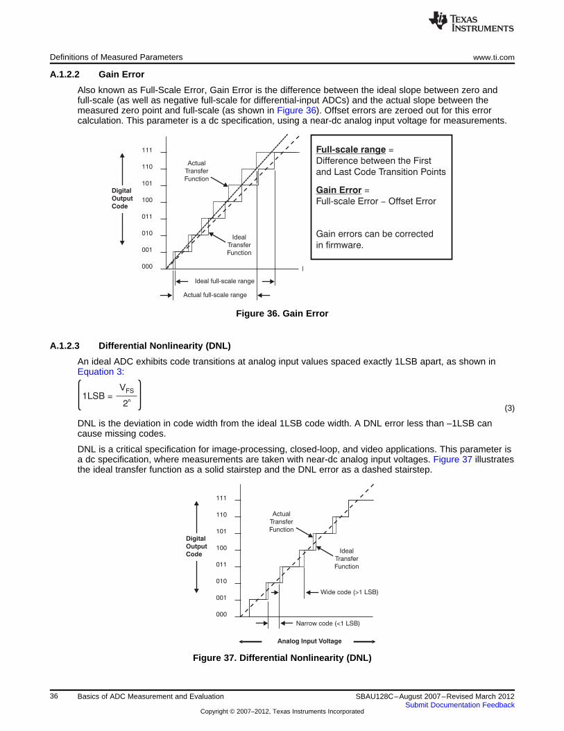
A.1.2.2 Gain Error
Also known as Full-Scale Error, Gain Error is the difference between the ideal slope between zero andfull-scale (as well as negative full-scale for differential-input ADCs) and the actual slope between themeasured zero point and full-scale (as shown in Figure 36). Offset errors are zeroed out for this errorcalculation. This parameter is a dc specification, using a near-dc analog input voltage for measurements.
Figure 36. Gain Error
A.1.2.3 Differential Nonlinearity (DNL)
An ideal ADC exhibits code transitions at analog input values spaced exactly 1LSB apart, as shown inEquation 3:
(3)
DNL is the deviation in code width from the ideal 1LSB code width. A DNL error less than –1LSB cancause missing codes.
DNL is a critical specification for image-processing, closed-loop, and video applications. This parameter isa dc specification, where measurements are taken with near-dc analog input voltages. Figure 37 illustratesthe ideal transfer function as a solid stairstep and the DNL error as a dashed stairstep.
Figure 37. Differential Nonlinearity (DNL)
36 Basics of ADC Measurement and Evaluation SBAU128C–August 2007–Revised March 2012Submit Documentation Feedback
Copyright © 2007–2012, Texas Instruments Incorporated
000
Analog Input Voltage
001
010
011
100
101
110
111
Digital
Output
Code
INL < 0
Actual
Transfer
Function
Ideal
Transfer
Function
INL < 0
INL = maximum deviation
between an ( line) code
transition point and its corresponding
( line) transition point,
after gain and offset error have
been removed.
actual dashed
ideal solid
Positive INL means
transition(s) later than ideal
Negative INL means
transition(s) earlier than ideal
A: Fundamental Signal Magnitude
B: Headroom = 0.5dB
C. Signal-to-Noise Ratio = 85dB
D: Spurious Free Dynamic Range = 96dB
E: Average Noise Floor = 125dB
F: First Harmonic Magnitude = 105dB
G: Second Harmonic Magnitude = 96dB
-
-
-
-
-
-
A
B
C
D
E
F G
0
-20
-40
-60
-80
-100
-120
-140
-160
Am
plit
ud
e (
dB
)
0 10 20 30 40 50
Frequency (kHz)
FREQUENCY SPECTRUM
(8192 point FFT, F = 10.0022kHz, 0.2dB)IN -
www.ti.com Definitions of Measured Parameters
A.1.2.4 Integral Nonlinearity (INL)
INL is also known as Relative Accuracy Error. INL is the maximum deviation of a transition point from thecorresponding point of the ideal transfer curve, with the measured offset and gain errors zeroed. INL isshown in Figure 38.
Figure 38. Integral Nonlinearity (INL)
This specification can be referenced to a best-fit transfer function or an end-point transfer function. Thebest-fit INL results will be one-half the error of the end-point measurement method for the same device.The best-fit transfer function is determined with a least squares curve fit to the transfer function. Thisparameter is a dc specification, where measurements are taken with near-dc analog input voltages. Theunits for INL are LSB.
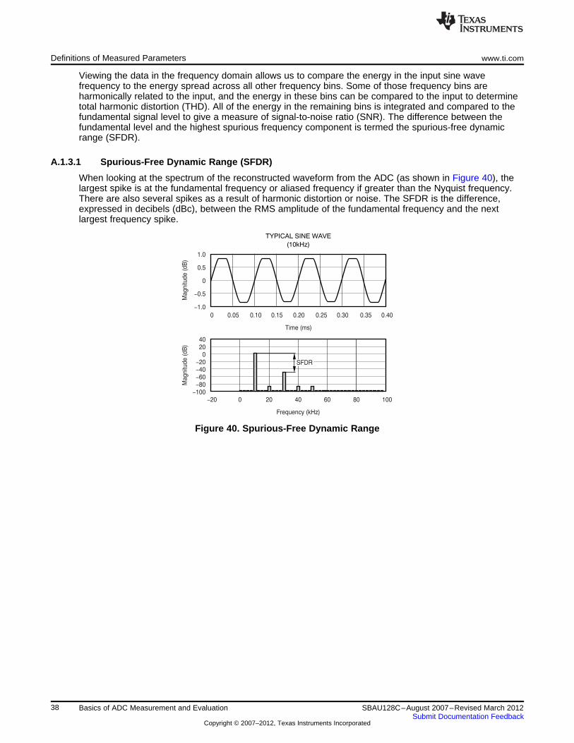
A.1.3 AC Parameters
While Section A.1.2.4 described dc (static) characteristics, ac (dynamic) characteristics of an ADC areoften more important, depending upon the application. Figure 39 shows the response of a converter to asine wave input and shows the output data in the frequency domain.
Figure 39. AC Parameters
37SBAU128C–August 2007–Revised March 2012 Basics of ADC Measurement and EvaluationSubmit Documentation Feedback
Copyright © 2007–2012, Texas Instruments Incorporated
1.0
0.5
0
-0.5
-1.0
Magnitu
de (
dB
)
TYPICAL SINE WAVE
(10kHz)
-20 0 20 40 60
Frequency (kHz)
80 100
0 0.05 0.10 0.15 0.20
Time (ms)
0.25 0.30 0.35 0.40
4020
0-20-40-60-80
-100
Magnitu
de (
dB
)
SFDR
Definitions of Measured Parameters www.ti.com
Viewing the data in the frequency domain allows us to compare the energy in the input sine wavefrequency to the energy spread across all other frequency bins. Some of those frequency bins areharmonically related to the input, and the energy in these bins can be compared to the input to determinetotal harmonic distortion (THD). All of the energy in the remaining bins is integrated and compared to thefundamental signal level to give a measure of signal-to-noise ratio (SNR). The difference between thefundamental level and the highest spurious frequency component is termed the spurious-free dynamicrange (SFDR).
A.1.3.1 Spurious-Free Dynamic Range (SFDR)
When looking at the spectrum of the reconstructed waveform from the ADC (as shown in Figure 40), thelargest spike is at the fundamental frequency or aliased frequency if greater than the Nyquist frequency.There are also several spikes as a result of harmonic distortion or noise. The SFDR is the difference,expressed in decibels (dBc), between the RMS amplitude of the fundamental frequency and the nextlargest frequency spike.
Figure 40. Spurious-Free Dynamic Range
38 Basics of ADC Measurement and Evaluation SBAU128C–August 2007–Revised March 2012Submit Documentation Feedback
Copyright © 2007–2012, Texas Instruments Incorporated

2F0 3F0 4F0 5F0 6F0 7F0 8F0 9F0
Harmonic Bins
Fundamental (F0)
www.ti.com Definitions of Measured Parameters
A.1.3.2 Total Harmonic Distortion (THD)
Total Harmonic Distortion (THD) measures the distortion provided in the reconstructed ADC signalresulting from harmonics of the fundamental frequency being generated by the ADC. THD does notinclude noise sources in the ADC, and this separates distortion in the ADC from noise generation.
THD is defined as the ratio, expressed in decibels (dBc), between the RMS value of the fundamentalfrequency component and the RMS sum of the first several (possibly aliased) harmonics of the inputfrequency.
IEEE1241-2000 specifies that THD should be measured by including the energy in the first nine harmonicbins.
Figure 41. Fundamental and Harmonic Bins
A.1.3.3 Signal-to-Noise Ratio (SNR)
The Signal-to-Noise Ratio (SNR) is the complementary measurement to THD. Here, a ratio is takenbetween the RMS sum of all the noise from dc (not including dc) to the Nyquist frequency, excluding theADC harmonics (possibly aliased) of the fundamental. That is, the RMS sum is taken over all thefrequency bins that are not used in the THD calculation above; therefore, typically harmonics above thefirst nine bins are treated as noise. If one assumes that the noise is independent of the signal, then theSNR is appropriately expressed in terms of dBFS—decibels with respect to the power of a sine waveencompassing the full-scale of the ADC.
A.1.3.4 SINAD
Sometimes called SNRD, this measurement expresses the Signal-to-Noise Ratio of the converterconsidering both harmonic distortion and noise. SINAD (Signal-to-Noise + Distortion Ratio) is calculatedby taking the RMS sum of all components except the fundamental summed from dc (not including dc) tothe Nyquist value, divided by the power of the fundamental sine wave input.
39SBAU128C–August 2007–Revised March 2012 Basics of ADC Measurement and EvaluationSubmit Documentation Feedback
Copyright © 2007–2012, Texas Instruments Incorporated

ENOB =(SINAD 1.76dB)-
6.02
2 =ENOB Full-scale
Noise
2M
s (ADC Codes)=
1LSB =V
FS
2n
ENOB = M log ( )- s2
SNR = 20 log = 6.02 N1
Noise
ENOB = N = 20 log6.02
1
ppm
ENOB = 20 log = 21.3 Bits6.02
1
0.4e-6
Definitions of Measured Parameters www.ti.com
A.1.3.5 Equivalent Number of Bits (ENOB)
Using either the SNR or SINAD value, the equivalent number of bits of an ideal ADC can be calculated,assuming only quantization noise exists. Generally the SINAD value is used.
IEEE-1241, and many manufacturers, use the concept of Effective Number of Bits (ENOB) to describeADC performance. ENOB is a figure of merit that is calculated from the SINAD or THD+N measurementdone using FFT testing. It attempts to describe the converter performance in terms of an ideal converter.For example, 16-bit converter that has 92dB SINAD that equates to an ideal converter of about 15 bits.This correspondence is found by using Equation 4 that simply uses the SNR equation for an idealconverter and solves it for N, and uses SINAD instead of SNR because a real converter will have artifactsother than quantization noise in the result.
(4)
As a simple figure of merit, ENOB (or SINAD) has its place. It does explain actual non-idealities of theconverter. For example, is there a linearity problem that causes poor THD, or does the converter just havemore noise? In the latter case, the user may have a usable converter if post-processing the data byaveraging or digital filtering.
Another issue with ENOB is that depending upon the type of converter the user is considering, themeasurement and specification of ENOB may not be what was expected. The method approved by theIEEE is a dynamic measurement, which requires a sine wave input. This dynamic measurement is usedwith converters of many different architectures and applies well for comparing dynamic performance.
However, manufacturers of delta-sigma converters for use in dc measurement applications have defined adifferent equation for ENOB that uses a noise measurement value. Note that the full-scale range iscompared to the noise:
(5)
(6)
(7)
Noise in these dc-precision converters can also be specified as ppm of full-scale:
(8)
(9)
For example, if noise = 0.4 ppm
(10)
Thus, in one case (Equation 4) the user is looking at a dynamic performance measurement of linearity andnoise, and in the second case (Equation 7) the user is looking at a noise measurement only.
40 Basics of ADC Measurement and Evaluation SBAU128C–August 2007–Revised March 2012Submit Documentation Feedback
Copyright © 2007–2012, Texas Instruments Incorporated

THD = ´ 100%Erms
N
i = 1
å1
N[E (i)]L
2
THD+N = ´ 100%Erms
N
i = 1
å1
N[E (i) + E (i) + E (i)]L Q N
2
www.ti.com Definitions of Measured Parameters
A.1.4 THD as a Proxy for Linearity
Being able to measure the THD allows us to examine the linearity of the ADC transfer function. Thismethod is a much easier way of looking at the device linearity than using dc techniques. In a perfectlylinear system, there would be no harmonic components created when the sine wave passes through theADC.
How exactly is THD related to linearity? This is a simple question with a complex answer. THD can befound from the linearity error at every code in the transfer function shown in Equation 11:
(11)
Alternatively, if including noise, the THD+N (or SINAD) can be found by including the quantization noiseand residual noise sources as shown in Equation 12:
where:• EL(I) is the linearity error at each sample;• EQ(I) is the quantization error at each sample; and• EN(I) is the residual noise at each sample. (12)
If we know the linearity error at every code along the ADC transfer function, then using Equation 11should allow us to calculate THD. If we wish to predict THD plus Noise (THD+N, also called SINAD), thenwe must also include random noise and quantization noise in this calculation, as illustrated in Equation 12.
Given a set of linearity data, one can predict THD; but given a THD value, one cannot determine linearityerrors directly, because THD is an integrated measurement of linearity.
41SBAU128C–August 2007–Revised March 2012 Basics of ADC Measurement and EvaluationSubmit Documentation Feedback
Copyright © 2007–2012, Texas Instruments Incorporated
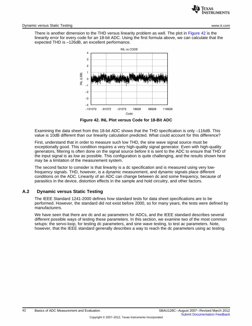
INL vs CODE
INL (
LS
B)
Code
4
3
2
1
0
-1
-2
-3
-4
-131072 -31072 18928 68928-81072 118928
Dynamic versus Static Testing www.ti.com
There is another dimension to the THD versus linearity problem as well. The plot in Figure 42 is thelinearity error for every code for an 18-bit ADC. Using the first formula above, we can calculate that theexpected THD is –126dB, an excellent performance.
Figure 42. INL Plot versus Code for 18-Bit ADC
Examining the data sheet from this 18-bit ADC shows that the THD specification is only –116dB. Thisvalue is 10dB different than our linearity calculation predicted. What could account for this difference?
First, understand that in order to measure such low THD, the sine wave signal source must beexceptionally good. This condition requires a very high-quality signal generator. Even with high-qualitygenerators, filtering is often done on the signal source before it is sent to the ADC to ensure that THD ofthe input signal is as low as possible. This configuration is quite challenging, and the results shown heremay be a limitation of the measurement system.
The second factor to consider is that linearity is a dc specification and is measured using very low-frequency signals. THD, however, is a dynamic measurement, and dynamic signals place differentconditions on the ADC. Linearity of an ADC can change between dc and some frequency, because ofparasitics in the device, distortion effects in the sample and hold circuitry, and other factors.
A.2 Dynamic versus Static Testing
The IEEE Standard 1241-2000 defines how standard tests for data sheet specifications are to beperformed. However, the standard did not exist before 2000, so for many years, the tests were defined bymanufacturers.
We have seen that there are dc and ac parameters for ADCs, and the IEEE standard describes severaldifferent possible ways of testing these parameters. In this section, we examine two of the most commonsetups: the servo-loop, for testing dc parameters, and sine wave testing, to test ac parameters. Note,however, that the IEEE standard generally describes a way to reach the dc parameters using ac testing.
42 Basics of ADC Measurement and Evaluation SBAU128C–August 2007–Revised March 2012Submit Documentation Feedback
Copyright © 2007–2012, Texas Instruments Incorporated
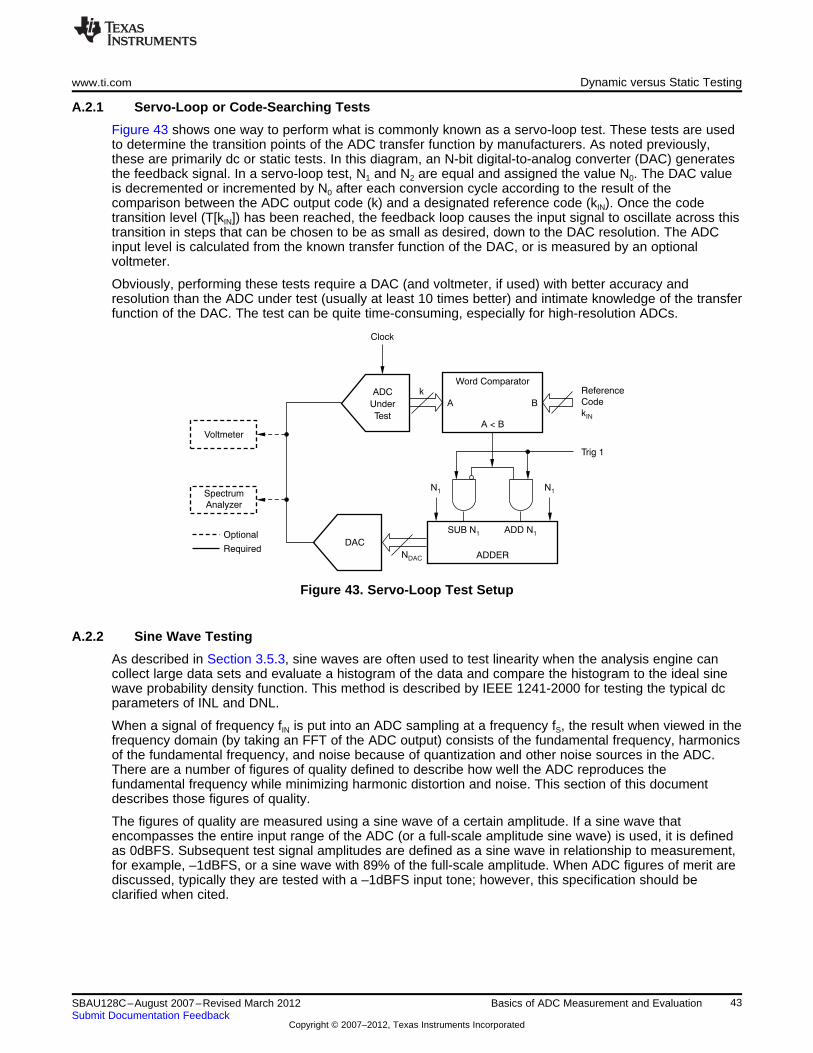
ADC
Under
Test
DAC
SUB N1
ADDER
ADD N1
A < B
Word Comparator
N1N1
k
NDAC
A B
Reference
Code
kIN
Trig 1
Clock
Voltmeter
Spectrum
Analyzer
Optional
Required
www.ti.com Dynamic versus Static Testing
A.2.1 Servo-Loop or Code-Searching Tests
Figure 43 shows one way to perform what is commonly known as a servo-loop test. These tests are usedto determine the transition points of the ADC transfer function by manufacturers. As noted previously,these are primarily dc or static tests. In this diagram, an N-bit digital-to-analog converter (DAC) generatesthe feedback signal. In a servo-loop test, N1 and N2 are equal and assigned the value N0. The DAC valueis decremented or incremented by N0 after each conversion cycle according to the result of thecomparison between the ADC output code (k) and a designated reference code (kIN). Once the codetransition level (T[kIN]) has been reached, the feedback loop causes the input signal to oscillate across thistransition in steps that can be chosen to be as small as desired, down to the DAC resolution. The ADCinput level is calculated from the known transfer function of the DAC, or is measured by an optionalvoltmeter.
Obviously, performing these tests require a DAC (and voltmeter, if used) with better accuracy andresolution than the ADC under test (usually at least 10 times better) and intimate knowledge of the transferfunction of the DAC. The test can be quite time-consuming, especially for high-resolution ADCs.
Figure 43. Servo-Loop Test Setup
A.2.2 Sine Wave Testing
As described in Section 3.5.3, sine waves are often used to test linearity when the analysis engine cancollect large data sets and evaluate a histogram of the data and compare the histogram to the ideal sinewave probability density function. This method is described by IEEE 1241-2000 for testing the typical dcparameters of INL and DNL.
When a signal of frequency fIN is put into an ADC sampling at a frequency fS, the result when viewed in thefrequency domain (by taking an FFT of the ADC output) consists of the fundamental frequency, harmonicsof the fundamental frequency, and noise because of quantization and other noise sources in the ADC.There are a number of figures of quality defined to describe how well the ADC reproduces thefundamental frequency while minimizing harmonic distortion and noise. This section of this documentdescribes those figures of quality.
The figures of quality are measured using a sine wave of a certain amplitude. If a sine wave thatencompasses the entire input range of the ADC (or a full-scale amplitude sine wave) is used, it is definedas 0dBFS. Subsequent test signal amplitudes are defined as a sine wave in relationship to measurement,for example, –1dBFS, or a sine wave with 89% of the full-scale amplitude. When ADC figures of merit arediscussed, typically they are tested with a –1dBFS input tone; however, this specification should beclarified when cited.
43SBAU128C–August 2007–Revised March 2012 Basics of ADC Measurement and EvaluationSubmit Documentation Feedback
Copyright © 2007–2012, Texas Instruments Incorporated

N = NCYC S
fIN
fS
Dynamic versus Static Testing www.ti.com
Figure 44 shows the test setup described in IEEE 1241-2000 for sine wave testing of an ADC. One sinesource is used most typically, but some tests take advantage of more than one signal (for example, to testfor intermodulation distortion). The clock generator is used as a clock for the ADC controlling the sampletime, and may be phase-locked to the sine wave generator to achieve coherent sampling.
Figure 44. Sine Wave Test Setup
A.2.2.1 Coherent Sampling
This section describes the selection of the sampling and input frequencies for the ADC characterizationthat allow the user to use no window function. There are two requirements on these frequencies. The firstrequirement is that the two frequencies be chosen so that there is no leakage in the FFT spectralcomponents. Second, the two frequencies are chosen so that an input waveform is sampled at differentphases each cycle, so that more information is added to the FFT every cycle.
Implicit in an FFT analysis is the assumption that the signal being sampled is replicated infinitely in timebefore and after the sequence being sampled; in the characterization environment this is not the case.Leakage results if there are discontinuities between the beginning and end of the sequence beingsampled. In order to prevent leakage in the FFT, it is necessary to sample the input frequency so that therecord time covers an integer number of periods of the input waveform. That is, the waveform must becontinuous when the record is duplicated forward and backward in time. The number of cycles of the inputsine wave in the record is given by Equation 13:
(13)
where Ncyc is chosen be an integer to prevent spectral leakage.
An example of a waveform that meets this requirement is illustrated in Figure 45. Selecting the number ofcycles (NCYC) to be an integer is called coherent sampling. Coherent sampling meets the first requirementof preventing FFT leakage.
44 Basics of ADC Measurement and Evaluation SBAU128C–August 2007–Revised March 2012Submit Documentation Feedback
Copyright © 2007–2012, Texas Instruments Incorporated

www.ti.com Dynamic versus Static Testing
To meet the second requirement that the input waveform be sampled at different phases during eachcycle of the input waveform, NCYC/NS is chosen to be an irreducible fraction—that is, NCYC and NS arechosen to be relatively prime. Since NS is typically chosen to be a power of two so that a radix-2 FFT canbe used, it suffices to choose NCYC to be an odd number. Note that Figure 45 does not meet thisrequirement because it has an even number of cycles in the data record. The coherent frequencycalculator included in the ADCPro (see Figure 32) allows the user to calculate a mutually prime coherentfrequency to simplify the process of choosing fIN.
Figure 45. Coherently-Sampled Waveform
45SBAU128C–August 2007–Revised March 2012 Basics of ADC Measurement and EvaluationSubmit Documentation Feedback
Copyright © 2007–2012, Texas Instruments Incorporated
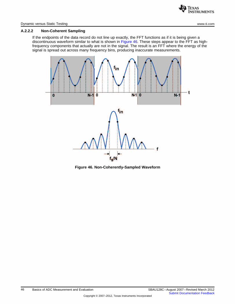
Dynamic versus Static Testing www.ti.com
A.2.2.2 Non-Coherent Sampling
If the endpoints of the data record do not line up exactly, the FFT functions as if it is being given adiscontinuous waveform similar to what is shown in Figure 46. These steps appear to the FFT as high-frequency components that actually are not in the signal. The result is an FFT where the energy of thesignal is spread out across many frequency bins, producing inaccurate measurements.
Figure 46. Non-Coherently-Sampled Waveform
46 Basics of ADC Measurement and Evaluation SBAU128C–August 2007–Revised March 2012Submit Documentation Feedback
Copyright © 2007–2012, Texas Instruments Incorporated

Input Data
x(n)
Window Function
w(n)
Windowed Input Data
w(n) x(n)´
t
t
t
n = 0 n = N 1-
Data Window
www.ti.com Tests and Equipment Requirements
A.2.2.3 Windowing
To fix this problem, a mathematical function can be applied to the data set that forces the endpoints tomatch, usually by driving them to zero as shown in Figure 47. This window function results in a data setas shown in the bottom trace; the frequency information of the waveform is preserved, but now theendpoints match, so the FFT gives more accurate results.
Many different windowing functions are available in the ADCPro software. For high-resolution converters(16-bits and above), high-order Blackman-Harris windows or the Low Sidelobe window give results similarto those of coherent sampling.
Figure 47. Windowing a Data Record
A.3 Tests and Equipment Requirements
From the preceding discussion, it should be clear that testing an ADC is complex. The simplest testingmethod is to use a sine wave signal source and look at the resulting data record in several ways. Thesemethods include time domain plots, histograms, and the FFT tests described previously. Using these threemethods together gives us a good indication of what the ADC transfer characteristics are.
When measuring high-performance ADCs, it is important to have a setup that can reveal the trueperformance of the ADC so that the test setup does not influence the results.
47SBAU128C–August 2007–Revised March 2012 Basics of ADC Measurement and EvaluationSubmit Documentation Feedback
Copyright © 2007–2012, Texas Instruments Incorporated

Tests and Equipment Requirements www.ti.com
A.3.1 Signal Source
In order to obtain meaningful results, the sine wave generator used in these tests must have distortion atleast 20dB below that expected from the ADC. For example, an ideal 16-bit converter (with no distortion atall) should measure a SINAD that is equal to the ideal SNR, or 98dB. The signal generator needed fortesting this type of converter would need to have THD+N less than –118dB at a minimum.
Unfortunately, most signal generators commonly found in labs are likely to have THD+N in the –70 to–80dB range. The Agilent 33120A™, a popular signal generator used in many labs, has about –78dBTHD+N at 1kHz—suitable for testing 9- or 10-bit converters, but nothing higher without following it withsome sort of very low distortion bandpass filter. An Audio Precision™ audio analyzer has a very goodsignal source if audio frequencies are suitable for the ADC under test. At higher frequencies, it becomesharder and harder to find generators that have very low distortion.
For the selection of a signal source, there are several qualities of merit that one should look for. Phasenoise, both close to the carrier and far out from the carrier, should be as low as possible and be devoid ofspurs. Spurious emissions must not exist; or, if they do exist, they must be located far enough from thecarrier such that they can be filtered out. A litmus test is to feed the signal source into a spectrum analyzerand verify that all spurs are indeed below the noise floor of the ADC. For best results, choose a signalsource with extremely low, close-in phase noise; use a narrow, high attenuation bandpass filter centeredon fIN.
ADC manufacturers spend the money to buy very high quality sine sources, preferably ones that can bephase-locked to the clock that is providing the sample clock, in order to do coherent sampling. Thesesources can cost $20,000 US or more.
A.3.2 Clock Source
In many modern high-performance ADCs, the converter sample-and-hold stage can accept either asinusoidal or square wave input. In these scenarios where the ADC can accept a sinusoidal input, thecomparator found at the front end has an extremely low jitter specification, or time domain uncertainty.Typically, these have better jitter performance than commercially-available pulse generators.Consequently, for maximum performance, it is advisable to use a sinusoidal source with extremely lowphase noise with a crystal bandpass filter centered on fS.
A.3.3 Other Equipment
The remaining equipment needed to perform ADC testing includes suitable power supplies, an evaluationboard for the ADC, and the means to collect data and analyze it. Many evaluation kits allow directconnection to a PC and software to analyze the data.
At TI, many of our ADC EVMs are produced in a modular format. This small card provides the minimalcircuitry needed to make the ADC operate—in some cases a reference voltage, or a clock source(oscillator) if needed. By itself, it provides a means for customers to connect the ADC into their ownsystems or test platforms. Using our modular EVM interface boards, these EVMs can be connected to TIprocessors for use in code development and hardware prototyping.
For evaluation only, the EVM alone is not enough. To address this need, we provide complete evaluationkits (identified by EVM-PDK). These kits consist of the modular EVM, plus a suitable motherboard to plugthem into, providing the means to collect data from the device and communicate that data to a computer,usually through a USB connection. EVM-PDKs that are supported by the ADCPro software also have anEVM plug-in installer that installs the necessary software to use the EVM-PDK with an ADCProinstallation.
48 Basics of ADC Measurement and Evaluation SBAU128C–August 2007–Revised March 2012Submit Documentation Feedback
Copyright © 2007–2012, Texas Instruments Incorporated

EVALUATION BOARD/KIT/MODULE (EVM) ADDITIONAL TERMS
Texas Instruments (TI) provides the enclosed Evaluation Board/Kit/Module (EVM) under the following conditions:
The user assumes all responsibility and liability for proper and safe handling of the goods. Further, the user indemnifies TI from all claimsarising from the handling or use of the goods.
Should this evaluation board/kit not meet the specifications indicated in the User’s Guide, the board/kit may be returned within 30 days fromthe date of delivery for a full refund. THE FOREGOING LIMITED WARRANTY IS THE EXCLUSIVE WARRANTY MADE BY SELLER TOBUYER AND IS IN LIEU OF ALL OTHER WARRANTIES, EXPRESSED, IMPLIED, OR STATUTORY, INCLUDING ANY WARRANTY OFMERCHANTABILITY OR FITNESS FOR ANY PARTICULAR PURPOSE. EXCEPT TO THE EXTENT OF THE INDEMNITY SET FORTHABOVE, NEITHER PARTY SHALL BE LIABLE TO THE OTHER FOR ANY INDIRECT, SPECIAL, INCIDENTAL, OR CONSEQUENTIALDAMAGES.
Please read the User's Guide and, specifically, the Warnings and Restrictions notice in the User's Guide prior to handling the product. Thisnotice contains important safety information about temperatures and voltages. For additional information on TI's environmental and/or safetyprograms, please visit www.ti.com/esh or contact TI.
No license is granted under any patent right or other intellectual property right of TI covering or relating to any machine, process, orcombination in which such TI products or services might be or are used. TI currently deals with a variety of customers for products, andtherefore our arrangement with the user is not exclusive. TI assumes no liability for applications assistance, customer product design,software performance, or infringement of patents or services described herein.
REGULATORY COMPLIANCE INFORMATION
As noted in the EVM User’s Guide and/or EVM itself, this EVM and/or accompanying hardware may or may not be subject to the FederalCommunications Commission (FCC) and Industry Canada (IC) rules.
For EVMs not subject to the above rules, this evaluation board/kit/module is intended for use for ENGINEERING DEVELOPMENT,DEMONSTRATION OR EVALUATION PURPOSES ONLY and is not considered by TI to be a finished end product fit for general consumeruse. It generates, uses, and can radiate radio frequency energy and has not been tested for compliance with the limits of computingdevices pursuant to part 15 of FCC or ICES-003 rules, which are designed to provide reasonable protection against radio frequencyinterference. Operation of the equipment may cause interference with radio communications, in which case the user at his own expense willbe required to take whatever measures may be required to correct this interference.
General Statement for EVMs including a radio
User Power/Frequency Use Obligations: This radio is intended for development/professional use only in legally allocated frequency andpower limits. Any use of radio frequencies and/or power availability of this EVM and its development application(s) must comply with locallaws governing radio spectrum allocation and power limits for this evaluation module. It is the user’s sole responsibility to only operate thisradio in legally acceptable frequency space and within legally mandated power limitations. Any exceptions to this are strictly prohibited andunauthorized by Texas Instruments unless user has obtained appropriate experimental/development licenses from local regulatoryauthorities, which is responsibility of user including its acceptable authorization.
For EVMs annotated as FCC – FEDERAL COMMUNICATIONS COMMISSION Part 15 Compliant
Caution
This device complies with part 15 of the FCC Rules. Operation is subject to the following two conditions: (1) This device may not causeharmful interference, and (2) this device must accept any interference received, including interference that may cause undesired operation.
Changes or modifications not expressly approved by the party responsible for compliance could void the user's authority to operate theequipment.
FCC Interference Statement for Class A EVM devices
This equipment has been tested and found to comply with the limits for a Class A digital device, pursuant to part 15 of the FCC Rules.These limits are designed to provide reasonable protection against harmful interference when the equipment is operated in a commercialenvironment. This equipment generates, uses, and can radiate radio frequency energy and, if not installed and used in accordance with theinstruction manual, may cause harmful interference to radio communications. Operation of this equipment in a residential area is likely tocause harmful interference in which case the user will be required to correct the interference at his own expense.
FCC Interference Statement for Class B EVM devices
This equipment has been tested and found to comply with the limits for a Class B digital device, pursuant to part 15 of the FCC Rules.These limits are designed to provide reasonable protection against harmful interference in a residential installation. This equipmentgenerates, uses and can radiate radio frequency energy and, if not installed and used in accordance with the instructions, may causeharmful interference to radio communications. However, there is no guarantee that interference will not occur in a particular installation. Ifthis equipment does cause harmful interference to radio or television reception, which can be determined by turning the equipment off andon, the user is encouraged to try to correct the interference by one or more of the following measures:
• Reorient or relocate the receiving antenna.• Increase the separation between the equipment and receiver.• Connect the equipment into an outlet on a circuit different from that to which the receiver is connected.• Consult the dealer or an experienced radio/TV technician for help.
For EVMs annotated as IC – INDUSTRY CANADA Compliant
This Class A or B digital apparatus complies with Canadian ICES-003.
Changes or modifications not expressly approved by the party responsible for compliance could void the user’s authority to operate theequipment.
Concerning EVMs including radio transmitters
This device complies with Industry Canada licence-exempt RSS standard(s). Operation is subject to the following two conditions: (1) thisdevice may not cause interference, and (2) this device must accept any interference, including interference that may cause undesiredoperation of the device.
Concerning EVMs including detachable antennas
Under Industry Canada regulations, this radio transmitter may only operate using an antenna of a type and maximum (or lesser) gainapproved for the transmitter by Industry Canada. To reduce potential radio interference to other users, the antenna type and its gain shouldbe so chosen that the equivalent isotropically radiated power (e.i.r.p.) is not more than that necessary for successful communication.
This radio transmitter has been approved by Industry Canada to operate with the antenna types listed in the user guide with the maximumpermissible gain and required antenna impedance for each antenna type indicated. Antenna types not included in this list, having a gaingreater than the maximum gain indicated for that type, are strictly prohibited for use with this device.
Cet appareil numérique de la classe A ou B est conforme à la norme NMB-003 du Canada.
Les changements ou les modifications pas expressément approuvés par la partie responsable de la conformité ont pu vider l’autorité del'utilisateur pour actionner l'équipement.
Concernant les EVMs avec appareils radio
Le présent appareil est conforme aux CNR d'Industrie Canada applicables aux appareils radio exempts de licence. L'exploitation estautorisée aux deux conditions suivantes : (1) l'appareil ne doit pas produire de brouillage, et (2) l'utilisateur de l'appareil doit accepter toutbrouillage radioélectrique subi, même si le brouillage est susceptible d'en compromettre le fonctionnement.
Concernant les EVMs avec antennes détachables
Conformément à la réglementation d'Industrie Canada, le présent émetteur radio peut fonctionner avec une antenne d'un type et d'un gainmaximal (ou inférieur) approuvé pour l'émetteur par Industrie Canada. Dans le but de réduire les risques de brouillage radioélectrique àl'intention des autres utilisateurs, il faut choisir le type d'antenne et son gain de sorte que la puissance isotrope rayonnée équivalente(p.i.r.e.) ne dépasse pas l'intensité nécessaire à l'établissement d'une communication satisfaisante.
Le présent émetteur radio a été approuvé par Industrie Canada pour fonctionner avec les types d'antenne énumérés dans le manueld’usage et ayant un gain admissible maximal et l'impédance requise pour chaque type d'antenne. Les types d'antenne non inclus danscette liste, ou dont le gain est supérieur au gain maximal indiqué, sont strictement interdits pour l'exploitation de l'émetteur.
SPACER
SPACER
SPACER
SPACER
SPACER
SPACER
SPACER
SPACER
【【Important Notice for Users of this Product in Japan】】This development kit is NOT certified as Confirming to Technical Regulations of Radio Law of Japan
If you use this product in Japan, you are required by Radio Law of Japan to follow the instructions below with respect to this product:
1. Use this product in a shielded room or any other test facility as defined in the notification #173 issued by Ministry of Internal Affairs andCommunications on March 28, 2006, based on Sub-section 1.1 of Article 6 of the Ministry’s Rule for Enforcement of Radio Law ofJapan,
2. Use this product only after you obtained the license of Test Radio Station as provided in Radio Law of Japan with respect to thisproduct, or
3. Use of this product only after you obtained the Technical Regulations Conformity Certification as provided in Radio Law of Japan withrespect to this product. Also, please do not transfer this product, unless you give the same notice above to the transferee. Please notethat if you could not follow the instructions above, you will be subject to penalties of Radio Law of Japan.
Texas Instruments Japan Limited(address) 24-1, Nishi-Shinjuku 6 chome, Shinjukku-ku, Tokyo, Japan
http://www.tij.co.jp
【ご使用にあたっての注】
本開発キットは技術基準適合証明を受けておりません。
本製品のご使用に際しては、電波法遵守のため、以下のいずれかの措置を取っていただく必要がありますのでご注意ください。1. 電波法施行規則第6条第1項第1号に基づく平成18年3月28日総務省告示第173号で定められた電波暗室等の試験設備でご使用いただく。2. 実験局の免許を取得後ご使用いただく。3. 技術基準適合証明を取得後ご使用いただく。
なお、本製品は、上記の「ご使用にあたっての注意」を譲渡先、移転先に通知しない限り、譲渡、移転できないものとします。
上記を遵守頂けない場合は、電波法の罰則が適用される可能性があることをご留意ください。
日本テキサス・インスツルメンツ株式会社東京都新宿区西新宿6丁目24番1号西新宿三井ビルhttp://www.tij.co.jp
SPACER
SPACER
SPACER
SPACER
SPACER
SPACER
SPACER
SPACER
SPACER
SPACER
SPACER
SPACER
SPACER
SPACER
SPACER
SPACER

EVALUATION BOARD/KIT/MODULE (EVM)WARNINGS, RESTRICTIONS AND DISCLAIMERS
For Feasibility Evaluation Only, in Laboratory/Development Environments. Unless otherwise indicated, this EVM is not a finishedelectrical equipment and not intended for consumer use. It is intended solely for use for preliminary feasibility evaluation inlaboratory/development environments by technically qualified electronics experts who are familiar with the dangers and application risksassociated with handling electrical mechanical components, systems and subsystems. It should not be used as all or part of a finished endproduct.
Your Sole Responsibility and Risk. You acknowledge, represent and agree that:
1. You have unique knowledge concerning Federal, State and local regulatory requirements (including but not limited to Food and DrugAdministration regulations, if applicable) which relate to your products and which relate to your use (and/or that of your employees,affiliates, contractors or designees) of the EVM for evaluation, testing and other purposes.
2. You have full and exclusive responsibility to assure the safety and compliance of your products with all such laws and other applicableregulatory requirements, and also to assure the safety of any activities to be conducted by you and/or your employees, affiliates,contractors or designees, using the EVM. Further, you are responsible to assure that any interfaces (electronic and/or mechanical)between the EVM and any human body are designed with suitable isolation and means to safely limit accessible leakage currents tominimize the risk of electrical shock hazard.
3. You will employ reasonable safeguards to ensure that your use of the EVM will not result in any property damage, injury or death, evenif the EVM should fail to perform as described or expected.
4. You will take care of proper disposal and recycling of the EVM’s electronic components and packing materials.
Certain Instructions. It is important to operate this EVM within TI’s recommended specifications and environmental considerations per theuser guidelines. Exceeding the specified EVM ratings (including but not limited to input and output voltage, current, power, andenvironmental ranges) may cause property damage, personal injury or death. If there are questions concerning these ratings please contacta TI field representative prior to connecting interface electronics including input power and intended loads. Any loads applied outside of thespecified output range may result in unintended and/or inaccurate operation and/or possible permanent damage to the EVM and/orinterface electronics. Please consult the EVM User's Guide prior to connecting any load to the EVM output. If there is uncertainty as to theload specification, please contact a TI field representative. During normal operation, some circuit components may have case temperaturesgreater than 60°C as long as the input and output are maintained at a normal ambient operating temperature. These components includebut are not limited to linear regulators, switching transistors, pass transistors, and current sense resistors which can be identified using theEVM schematic located in the EVM User's Guide. When placing measurement probes near these devices during normal operation, pleasebe aware that these devices may be very warm to the touch. As with all electronic evaluation tools, only qualified personnel knowledgeablein electronic measurement and diagnostics normally found in development environments should use these EVMs.
Agreement to Defend, Indemnify and Hold Harmless. You agree to defend, indemnify and hold TI, its licensors and their representativesharmless from and against any and all claims, damages, losses, expenses, costs and liabilities (collectively, "Claims") arising out of or inconnection with any use of the EVM that is not in accordance with the terms of the agreement. This obligation shall apply whether Claimsarise under law of tort or contract or any other legal theory, and even if the EVM fails to perform as described or expected.
Safety-Critical or Life-Critical Applications. If you intend to evaluate the components for possible use in safety critical applications (suchas life support) where a failure of the TI product would reasonably be expected to cause severe personal injury or death, such as deviceswhich are classified as FDA Class III or similar classification, then you must specifically notify TI of such intent and enter into a separateAssurance and Indemnity Agreement.
Mailing Address: Texas Instruments, Post Office Box 655303, Dallas, Texas 75265Copyright © 2012, Texas Instruments Incorporated
IMPORTANT NOTICE
Texas Instruments Incorporated and its subsidiaries (TI) reserve the right to make corrections, modifications, enhancements, improvements,and other changes to its products and services at any time and to discontinue any product or service without notice. Customers shouldobtain the latest relevant information before placing orders and should verify that such information is current and complete. All products aresold subject to TI’s terms and conditions of sale supplied at the time of order acknowledgment.
TI warrants performance of its hardware products to the specifications applicable at the time of sale in accordance with TI’s standardwarranty. Testing and other quality control techniques are used to the extent TI deems necessary to support this warranty. Except wheremandated by government requirements, testing of all parameters of each product is not necessarily performed.
TI assumes no liability for applications assistance or customer product design. Customers are responsible for their products andapplications using TI components. To minimize the risks associated with customer products and applications, customers should provideadequate design and operating safeguards.
TI does not warrant or represent that any license, either express or implied, is granted under any TI patent right, copyright, mask work right,or other TI intellectual property right relating to any combination, machine, or process in which TI products or services are used. Informationpublished by TI regarding third-party products or services does not constitute a license from TI to use such products or services or awarranty or endorsement thereof. Use of such information may require a license from a third party under the patents or other intellectualproperty of the third party, or a license from TI under the patents or other intellectual property of TI.
Reproduction of TI information in TI data books or data sheets is permissible only if reproduction is without alteration and is accompaniedby all associated warranties, conditions, limitations, and notices. Reproduction of this information with alteration is an unfair and deceptivebusiness practice. TI is not responsible or liable for such altered documentation. Information of third parties may be subject to additionalrestrictions.
Resale of TI products or services with statements different from or beyond the parameters stated by TI for that product or service voids allexpress and any implied warranties for the associated TI product or service and is an unfair and deceptive business practice. TI is notresponsible or liable for any such statements.
TI products are not authorized for use in safety-critical applications (such as life support) where a failure of the TI product would reasonablybe expected to cause severe personal injury or death, unless officers of the parties have executed an agreement specifically governingsuch use. Buyers represent that they have all necessary expertise in the safety and regulatory ramifications of their applications, andacknowledge and agree that they are solely responsible for all legal, regulatory and safety-related requirements concerning their productsand any use of TI products in such safety-critical applications, notwithstanding any applications-related information or support that may beprovided by TI. Further, Buyers must fully indemnify TI and its representatives against any damages arising out of the use of TI products insuch safety-critical applications.
TI products are neither designed nor intended for use in military/aerospace applications or environments unless the TI products arespecifically designated by TI as military-grade or "enhanced plastic." Only products designated by TI as military-grade meet militaryspecifications. Buyers acknowledge and agree that any such use of TI products which TI has not designated as military-grade is solely atthe Buyer's risk, and that they are solely responsible for compliance with all legal and regulatory requirements in connection with such use.
TI products are neither designed nor intended for use in automotive applications or environments unless the specific TI products aredesignated by TI as compliant with ISO/TS 16949 requirements. Buyers acknowledge and agree that, if they use any non-designatedproducts in automotive applications, TI will not be responsible for any failure to meet such requirements.
Following are URLs where you can obtain information on other Texas Instruments products and application solutions:
Products Applications
Audio www.ti.com/audio Automotive and Transportation www.ti.com/automotive
Amplifiers amplifier.ti.com Communications and Telecom www.ti.com/communications
Data Converters dataconverter.ti.com Computers and Peripherals www.ti.com/computers
DLP® Products www.dlp.com Consumer Electronics www.ti.com/consumer-apps
DSP dsp.ti.com Energy and Lighting www.ti.com/energy
Clocks and Timers www.ti.com/clocks Industrial www.ti.com/industrial
Interface interface.ti.com Medical www.ti.com/medical
Logic logic.ti.com Security www.ti.com/security
Power Mgmt power.ti.com Space, Avionics and Defense www.ti.com/space-avionics-defense
Microcontrollers microcontroller.ti.com Video and Imaging www.ti.com/video
RFID www.ti-rfid.com
OMAP Mobile Processors www.ti.com/omap
Wireless Connectivity www.ti.com/wirelessconnectivity
TI E2E Community Home Page e2e.ti.com
Mailing Address: Texas Instruments, Post Office Box 655303, Dallas, Texas 75265Copyright © 2012, Texas Instruments Incorporated