ad7862 simultaneous sampling dual 250 ksps 12-bit...
TRANSCRIPT

REV. 0
Information furnished by Analog Devices is believed to be accurate andreliable. However, no responsibility is assumed by Analog Devices for itsuse, nor for any infringements of patents or other rights of third partieswhich may result from its use. No license is granted by implication orotherwise under any patent or patent rights of Analog Devices.
a
AD7862
One Technology Way, P.O. Box 9106, Norwood, MA 02062-9106, U.S.A.
Tel: 617/329-4700 World Wide Web Site: http://www.analog.com
Fax: 617/326-8703 © Analog Devices, Inc., 1996
Simultaneous SamplingDual 250 kSPS 12-Bit ADC
FUNCTIONAL BLOCK DIAGRAM
CLOCK
DGND
DB0
BUSY
RD
CS
CONVST
AD7862
CONVERSIONCONTROL LOGIC
VA1
AGND
VREF
+2.5VREFERENCE2kΩ
AGND
TRACK/HOLD
VDD
DB11
OUTPUTLATCH
MUX
A0
12-BITADC
12-BITADC
TRACK/HOLD
MUX
SIGNALSCALING
SIGNALSCALING
SIGNALSCALING
SIGNALSCALING
VB1
VA2
VB2
FEATURES
Two Fast 12-Bit ADCs
Four Input Channels
Simultaneous Sampling & Conversion
4 ms Throughput Time
Single Supply Operation
Selection of Input Ranges:
610 V for AD7862-10
62.5 V for AD7862-3
0 V to 2.5 V for AD7862-2
High Speed Parallel Interface
Low Power, 60 mW typ
Power Saving Mode, 50 mW typ
Overvoltage Protection on Analog Inputs
14-Bit Pin Compatible Upgrade (AD7863)
APPLICATIONS
AC Motor Control
Uninterrupted Power Supplies
Data Acquisition Systems
Communications
GENERAL DESCRIPTIONThe AD7862 is a high speed, low power, dual 12-bit A/Dconverter that operates from a single +5 V supply. The partcontains two 4 µs successive approximation ADCs, two track/hold amplifiers, an internal +2.5 V reference and a high speedparallel interface. There are four analog inputs that are groupedinto two channels (A & B) selected by the A0 input. Eachchannel has two inputs (VA1 & VA2 or VB1 & VB2) that can besampled and converted simultaneously thus preserving therelative phase information of the signals on both analog inputs.The part accepts an analog input range of ±10 V (AD7862-10),±2.5 V (AD7862-3) and 0–2.5 V (AD7862-2). Overvoltageprotection on the analog inputs for the part allows the inputvoltage to go to ±17 V, ±7 V or +7 V, respectively, withoutcausing damage.
A single conversion start signal (CONVST) places both track/holds into hold simultaneously and initiates conversion on bothinputs. The BUSY signal indicates the end of conversion, andat this time the conversion results for both channels are avail-able to be read. The first read after a conversion accesses theresult from VA1 or VB1, while the second read accesses the resultfrom VA2 or VB2, depending on whether the multiplexer selectA0 is low or high, respectively. Data is read from the part via a12-bit parallel data bus with standard CS and RD signals.
In addition to the traditional dc accuracy specifications such aslinearity, full-scale and offset errors, the part is also specified fordynamic performance parameters including harmonic distortionand signal-to-noise ratio.
The AD7862 is fabricated in Analog Devices’ Linear Compat-ible CMOS (LC2MOS) process, a mixed technology processthat combines precision bipolar circuits with low power CMOSlogic. It is available in 28-lead SSOP, SOIC and DIP.
PRODUCT HIGHLIGHTS1. The AD7862 features two complete ADC functions allowing
simultaneous sampling and conversion of two channels. EachADC has a 2-channel input mux. The conversion result forboth channels is available 3.6 µs after initiating conversion.
2. The AD7862 operates from a single +5 V supply andconsumes 60 mW typ. The automatic power-down mode,where the part goes into power down once conversion iscomplete and “wakes up” before the next conversion cycle,makes the AD7862 ideal for battery-powered or portableapplications.
3. The part offers a high speed parallel interface for easy con-nection to microprocessors, microcontrollers and digitalsignal processors.
4. The part is offered in three versions with different analoginput ranges. The AD7862-10 offers the standard industrialinput range of ±10 V; the AD7862-3 offers the commonsignal processing input range of ±2.5 V; while the AD7862-2can be used in unipolar 0 V – +2.5 V applications.
5. The part features very tight aperture delay matching betweenthe two input sample-and-hold amplifiers.
–2– REV. 0
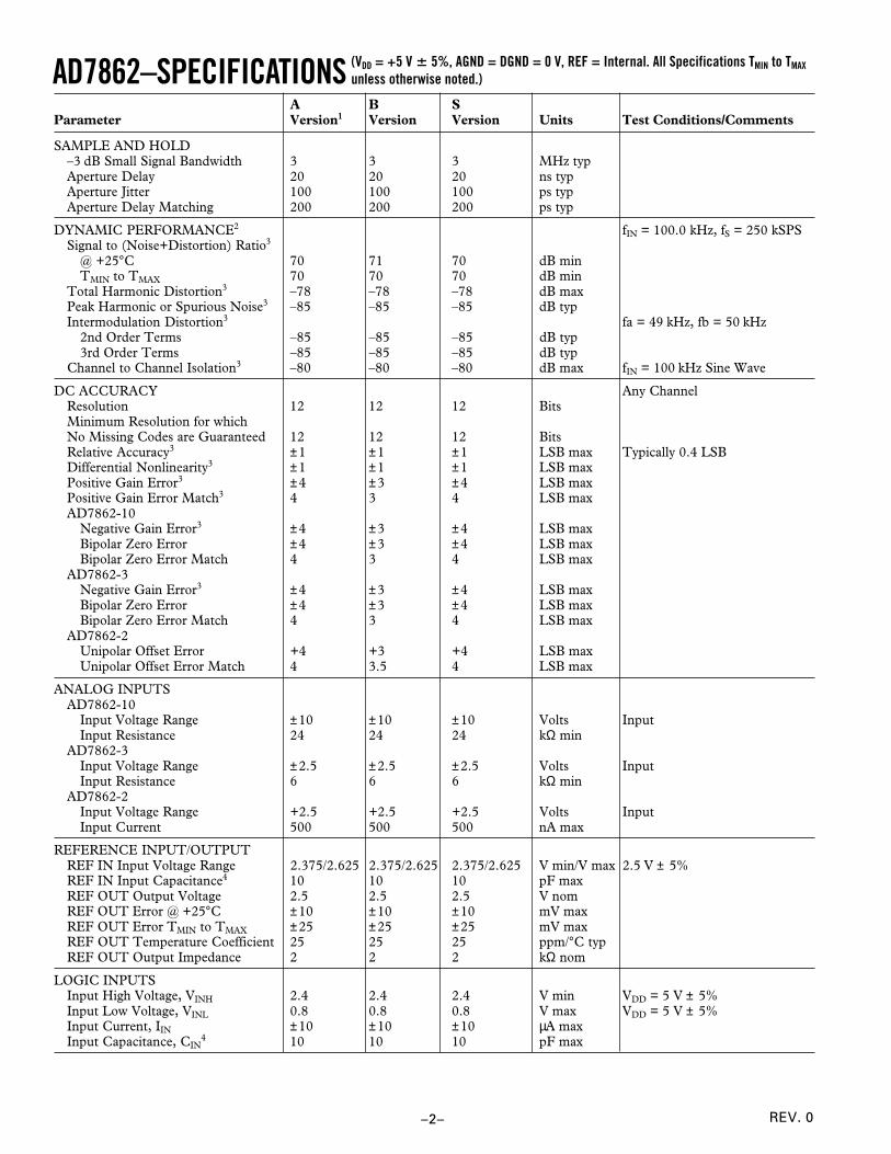
AD7862–SPECIFICATIONSA B S
Parameter Version1 Version Version Units Test Conditions/Comments
SAMPLE AND HOLD–3 dB Small Signal Bandwidth 3 3 3 MHz typAperture Delay 20 20 20 ns typAperture Jitter 100 100 100 ps typAperture Delay Matching 200 200 200 ps typ
DYNAMIC PERFORMANCE2 fIN = 100.0 kHz, fS = 250 kSPSSignal to (Noise+Distortion) Ratio3
@ +25°C 70 71 70 dB minTMIN to TMAX 70 70 70 dB min
Total Harmonic Distortion3 –78 –78 –78 dB maxPeak Harmonic or Spurious Noise3 –85 –85 –85 dB typIntermodulation Distortion3 fa = 49 kHz, fb = 50 kHz
2nd Order Terms –85 –85 –85 dB typ3rd Order Terms –85 –85 –85 dB typ
Channel to Channel Isolation3 –80 –80 –80 dB max fIN = 100 kHz Sine Wave
DC ACCURACY Any ChannelResolution 12 12 12 BitsMinimum Resolution for whichNo Missing Codes are Guaranteed 12 12 12 BitsRelative Accuracy3 ±1 ±1 ±1 LSB max Typically 0.4 LSBDifferential Nonlinearity3 ±1 ±1 ±1 LSB maxPositive Gain Error3 ±4 ±3 ±4 LSB maxPositive Gain Error Match3 4 3 4 LSB maxAD7862-10
Negative Gain Error3 ±4 ±3 ±4 LSB maxBipolar Zero Error ±4 ±3 ±4 LSB maxBipolar Zero Error Match 4 3 4 LSB max
AD7862-3Negative Gain Error3 ±4 ±3 ±4 LSB maxBipolar Zero Error ±4 ±3 ±4 LSB maxBipolar Zero Error Match 4 3 4 LSB max
AD7862-2Unipolar Offset Error +4 +3 +4 LSB maxUnipolar Offset Error Match 4 3.5 4 LSB max
ANALOG INPUTSAD7862-10
Input Voltage Range ±10 ±10 ±10 Volts InputInput Resistance 24 24 24 kΩ min
AD7862-3Input Voltage Range ±2.5 ±2.5 ±2.5 Volts InputInput Resistance 6 6 6 kΩ min
AD7862-2Input Voltage Range +2.5 +2.5 +2.5 Volts InputInput Current 500 500 500 nA max
REFERENCE INPUT/OUTPUTREF IN Input Voltage Range 2.375/2.625 2.375/2.625 2.375/2.625 V min/V max 2.5 V ± 5%REF IN Input Capacitance4 10 10 10 pF maxREF OUT Output Voltage 2.5 2.5 2.5 V nomREF OUT Error @ +25°C ±10 ±10 ±10 mV maxREF OUT Error TMIN to TMAX ±25 ±25 ±25 mV maxREF OUT Temperature Coefficient 25 25 25 ppm/°C typREF OUT Output Impedance 2 2 2 kΩ nom
LOGIC INPUTSInput High Voltage, VINH 2.4 2.4 2.4 V min VDD = 5 V ± 5%Input Low Voltage, VINL 0.8 0.8 0.8 V max VDD = 5 V ± 5%Input Current, IIN ±10 ±10 ±10 µA maxInput Capacitance, CIN
4 10 10 10 pF max
(VDD = +5 V 6 5%, AGND = DGND = 0 V, REF = Internal. All Specifications TMIN to TMAX
unless otherwise noted.)
–3–REV. 0
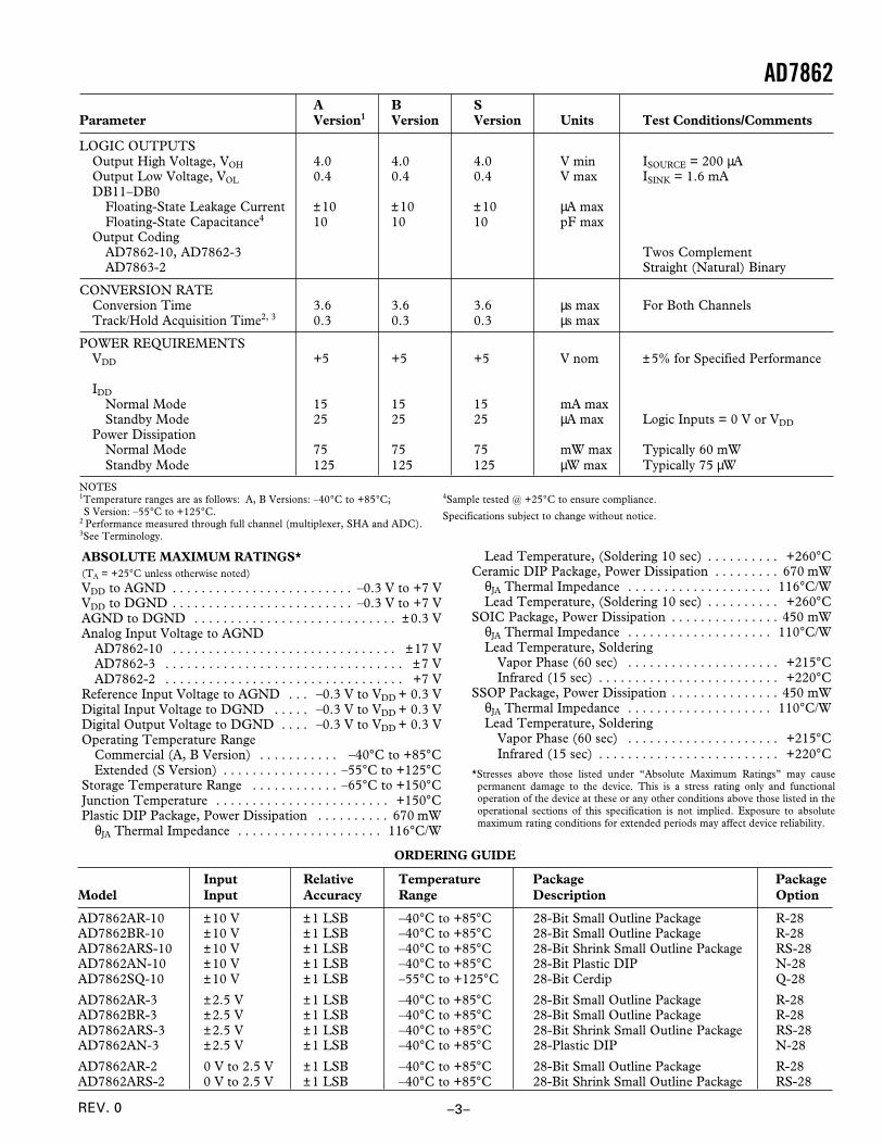
AD7862A B S
Parameter Version1 Version Version Units Test Conditions/Comments
LOGIC OUTPUTSOutput High Voltage, VOH 4.0 4.0 4.0 V min ISOURCE = 200 µAOutput Low Voltage, VOL 0.4 0.4 0.4 V max ISINK = 1.6 mADB11–DB0
Floating-State Leakage Current ±10 ±10 ±10 µA maxFloating-State Capacitance4 10 10 10 pF max
Output CodingAD7862-10, AD7862-3 Twos ComplementAD7863-2 Straight (Natural) Binary
CONVERSION RATEConversion Time 3.6 3.6 3.6 µs max For Both ChannelsTrack/Hold Acquisition Time2, 3 0.3 0.3 0.3 µs max
POWER REQUIREMENTSVDD +5 +5 +5 V nom ±5% for Specified Performance
IDD
Normal Mode 15 15 15 mA maxStandby Mode 25 25 25 µA max Logic Inputs = 0 V or VDD
Power DissipationNormal Mode 75 75 75 mW max Typically 60 mWStandby Mode 125 125 125 µW max Typically 75 µW
NOTES1Temperature ranges are as follows: A, B Versions: –40°C to +85°C;S Version: –55°C to +125°C.
2 Performance measured through full channel (multiplexer, SHA and ADC).3See Terminology.
ABSOLUTE MAXIMUM RATINGS*(TA = +25°C unless otherwise noted)
VDD to AGND . . . . . . . . . . . . . . . . . . . . . . . . . –0.3 V to +7 VVDD to DGND . . . . . . . . . . . . . . . . . . . . . . . . . –0.3 V to +7 VAGND to DGND . . . . . . . . . . . . . . . . . . . . . . . . . . . . ±0.3 VAnalog Input Voltage to AGND
AD7862-10 . . . . . . . . . . . . . . . . . . . . . . . . . . . . . . . ±17 VAD7862-3 . . . . . . . . . . . . . . . . . . . . . . . . . . . . . . . . . ±7 VAD7862-2 . . . . . . . . . . . . . . . . . . . . . . . . . . . . . . . . . +7 V
Reference Input Voltage to AGND . . . –0.3 V to VDD + 0.3 VDigital Input Voltage to DGND . . . . . –0.3 V to VDD + 0.3 VDigital Output Voltage to DGND . . . . –0.3 V to VDD + 0.3 VOperating Temperature Range
Commercial (A, B Version) . . . . . . . . . . . –40°C to +85°CExtended (S Version) . . . . . . . . . . . . . . . . –55°C to +125°C
Storage Temperature Range . . . . . . . . . . . . –65°C to +150°CJunction Temperature . . . . . . . . . . . . . . . . . . . . . . . . +150°CPlastic DIP Package, Power Dissipation . . . . . . . . . . 670 mW
θJA Thermal Impedance . . . . . . . . . . . . . . . . . . . . 116°C/W
Lead Temperature, (Soldering 10 sec) . . . . . . . . . . +260°CCeramic DIP Package, Power Dissipation . . . . . . . . . 670 mW
θJA Thermal Impedance . . . . . . . . . . . . . . . . . . . . 116°C/WLead Temperature, (Soldering 10 sec) . . . . . . . . . . +260°C
SOIC Package, Power Dissipation . . . . . . . . . . . . . . . 450 mWθJA Thermal Impedance . . . . . . . . . . . . . . . . . . . . 110°C/WLead Temperature, Soldering
Vapor Phase (60 sec) . . . . . . . . . . . . . . . . . . . . . +215°CInfrared (15 sec) . . . . . . . . . . . . . . . . . . . . . . . . . +220°C
SSOP Package, Power Dissipation . . . . . . . . . . . . . . . 450 mWθJA Thermal Impedance . . . . . . . . . . . . . . . . . . . . 110°C/WLead Temperature, Soldering
Vapor Phase (60 sec) . . . . . . . . . . . . . . . . . . . . . +215°CInfrared (15 sec) . . . . . . . . . . . . . . . . . . . . . . . . . +220°C
*Stresses above those listed under “Absolute Maximum Ratings” may causepermanent damage to the device. This is a stress rating only and functionaloperation of the device at these or any other conditions above those listed in theoperational sections of this specification is not implied. Exposure to absolutemaximum rating conditions for extended periods may affect device reliability.
ORDERING GUIDE
Input Relative Temperature Package PackageModel Input Accuracy Range Description Option
AD7862AR-10 ±10 V ±1 LSB –40°C to +85°C 28-Bit Small Outline Package R-28AD7862BR-10 ±10 V ±1 LSB –40°C to +85°C 28-Bit Small Outline Package R-28AD7862ARS-10 ±10 V ±1 LSB –40°C to +85°C 28-Bit Shrink Small Outline Package RS-28AD7862AN-10 ±10 V ±1 LSB –40°C to +85°C 28-Bit Plastic DIP N-28AD7862SQ-10 ±10 V ±1 LSB –55°C to +125°C 28-Bit Cerdip Q-28
AD7862AR-3 ±2.5 V ±1 LSB –40°C to +85°C 28-Bit Small Outline Package R-28AD7862BR-3 ±2.5 V ±1 LSB –40°C to +85°C 28-Bit Small Outline Package R-28AD7862ARS-3 ±2.5 V ±1 LSB –40°C to +85°C 28-Bit Shrink Small Outline Package RS-28AD7862AN-3 ±2.5 V ±1 LSB –40°C to +85°C 28-Plastic DIP N-28
AD7862AR-2 0 V to 2.5 V ±1 LSB –40°C to +85°C 28-Bit Small Outline Package R-28AD7862ARS-2 0 V to 2.5 V ±1 LSB –40°C to +85°C 28-Bit Shrink Small Outline Package RS-28
4Sample tested @ +25°C to ensure compliance.
Specifications subject to change without notice.

AD7862
–4– REV. 0
WARNING!
ESD SENSITIVE DEVICE
CAUTIONESD (electrostatic discharge) sensitive device. Electrostatic charges as high as 4000 V readilyaccumulate on the human body and test equipment and can discharge without detection.Although the AD7862 features proprietary ESD protection circuitry, permanent damage mayoccur on devices subjected to high energy electrostatic discharges. Therefore, proper ESDprecautions are recommended to avoid performance degradation or loss of functionality.
TIMING CHARACTERISTICS1, 2
A, B SParameter Versions Version Units Test Conditions/Comments
tCONV 3.6 3.6 µs max Conversion TimetACQ 0.3 0.3 us max Acquisition Time
Parallel Interfacet1 0 0 ns min CS to RD Setup Timet2 0 0 ns min CS to RD Hold Timet3 35 45 ns min CONVST Pulse Widtht4 35 45 ns min Read Pulse Widtht5
3 12 12 ns min Data Access Time After Falling Edge of RD60 70 ns max
t64 5 5 ns min Bus Relinquish Time After Rising Edge of RD
30 40 ns maxt7 40 40 ns min Time Between Consecutive Reads
NOTES1Sample tested at +25°C to ensure compliance. All input signals are measured with tr = tf = 1 ns (10% to 90% of +5 V) and timed from a voltage level of +1.6 V.2 See Figure 1.3Measured with the load circuit of Figure 2 and defined as the time required for an output to cross 0.8 V or 2.0 V.4These times are derived from the measured time taken by the data outputs to change 0.5 V when loaded with the circuit of Figure 2. The measured number is thenextrapolated back to remove the effects of charging or discharging the 50 pF capacitor. This means that the times quoted in the timing characteristics are the true busrelinquish times of the part and as such are independent of external bus loading capacitances.
Specifications subject to change without notice.
(VDD = +5 V 6 5%, AGND = DGND = 0 V, REF = Internal. All Specifications TMIN to TMAX unlessotherwise noted.)
VA1 VA2 VB1 VB2
t3
t1 t2
t4
t5 t6
tCONV
t7
CONVST
BUSY
A0
CS
RD
DATA
......... .........
Figure 1. Timing Diagram
+1.6V
1.6mA
200µA
50pF
TOOUTPUT
PIN
Figure 2. Load Circuit for Access Time and Bus Relinquish Time

AD7862
–5–REV. 0
PIN FUNCTION DESCRIPTION
Pin Mnemonic Description
1 NC No Connect2 DB11 Data Bit 11 (MSB). Three-state TTL output. Output coding is twos complement for the AD7862-
10 and AD7862-3. Output coding is straight (natural) binary for the AD7862-2.3–6 DB10–DB7 Data Bit 10 to Data Bit 7. Three-state TTL outputs.7 DGND Digital Ground. Ground reference for digital circuitry.8 CONVST Convert Start Input. Logic Input. A high to low transition on this input puts both track/holds into
their hold mode and starts conversion on both channels.9–15 DB6–DB0 Data Bit 6 to Data Bit 0. Three-state TTL outputs.16 AGND Analog Ground. Ground reference for mux, track/hold, reference and DAC circuitry.17 VB2 Input Number 2 of Channel B. Analog Input voltage ranges of ±10 V (AD7862-10), ±2.5 V
(AD7862-3) and 0 V–2.5 V (AD7862-2).18 VA2 Input Number 2 of Channel A. Analog Input voltage ranges of ±10 V (AD7862-10), ±2.5 V
(AD7862-3) and 0 V–2.5 V (AD7862-2).19 VREF Reference Input/Output. This pin is connected to the internal reference through a series resistor and is
the output reference source for the analog-to-digital converter. The nominal reference voltage is 2.5 V,and this appears at the pin.
20 A0 Multiplexer Select. This input is used in conjunction with RD and CS low to enable the data outputs.With A0 logic low, one read after a conversion will read the data from each of the ADCs in the sequence,VA1, VA2, and a subsequent read, when A0 goes high, reads the data from VB1, VB2.
21 CS Chip Select Input. Active low logic input. The device is selected when this input is active.22 RD Read Input. Active low logic input. This input is used in conjunction with A0 and CS low to enable
the data outputs. With A0 logic low, one read after a conversion will read the data from each of theADCs in the sequence, VA1, VA2, and a subsequent read, when A0 goes high, reads the data from VB1,VB2.
23 BUSY Busy Output. The busy output is triggered high by the falling edge of CONVST and remains highuntil conversion is completed.
24 VDD Analog and Digital Positive Supply Voltage, +5.0 V ± 5%.25 VA1 Input Number 1 of Channel A. Analog Input voltage ranges of ±10 V (AD7862-10), ±2.5 V
(AD7862-3) and 0 V–2.5 V (AD7862-2).26 VB1 Input Number 1 of Channel B. Analog Input voltage ranges of ±10 V (AD7862-10), ±2.5 V
(AD7862-3) and 0 V–2.5 V (AD7862-2).27 AGND Analog Ground. Ground reference for mux, track/hold, reference and DAC circuitry.28 NC No Connect
PIN CONFIGURATION
14
13
12
11
17
16
15
20
19
18
10
9
8
1
2
3
4
7
6
5
TOP VIEW(Not to Scale)
28
27
26
25
24
23
22
21
AD7862
NC = NO CONNECT
NC
VA1
VB1
AGND
NC
DB11
DB10
DB9
RD
BUSY
VDDDB8
DB7
DGND
CONVST
DB6
DB5 VREF
A0
CS
DB4
DB3
DB2
DB1
VA2
DB0
AGND
VB2

AD7862
–6– REV. 0
TERMINOLOGYSignal to (Noise + Distortion) RatioThis is the measured ratio of signal to (noise + distortion) at theoutput of the A/D converter. The signal is the rms amplitude ofthe fundamental. Noise is the rms sum of all nonfundamentalsignals up to half the sampling frequency (fS/2), excluding dc.The ratio is dependent upon the number of quantization levelsin the digitization process; the more levels, the smaller thequantization noise. The theoretical signal to (noise + distortion)ratio for an ideal N-bit converter with a sine wave input is givenby:
Signal to (Noise + Distortion) = (6.02 N + 1.76) dB
Thus for a 12-bit converter, this is 74 dB.
Total Harmonic DistortionTotal harmonic distortion (THD) is the ratio of the rms sum ofharmonics to the fundamental. For the AD7862 it is defined as:
THD dB( ) = 20 log
V22 +V3
2 +V42 +V5
2
V1
where V1 is the rms amplitude of the fundamental and V2, V3, V4
and V5 are the rms amplitudes of the second through the fifthharmonics.
Peak Harmonic or Spurious NoisePeak harmonic or spurious noise is defined as the ratio of therms value of the next largest component in the ADC outputspectrum (up to fS/2 and excluding dc) to the rms value of thefundamental. Normally, the value of this specification is deter-mined by the largest harmonic in the spectrum, but for partswhere the harmonics are buried in the noise floor, it will be anoise peak.
Intermodulation DistortionWith inputs consisting of sine waves at two frequencies, fa andfb, any active device with nonlinearities will create distortionproducts at sum and difference frequencies of mfa ± nfb wherem, n = 0, 1, 2, 3, etc. Intermodulation terms are those forwhich neither m nor n are equal to zero. For example, thesecond order terms include (fa + fb) and (fa – fb), while thethird order terms include (2 fa + fb), (2 fa – fb), (fa + 2 fb) and(fa – 2 fb).
The AD7862 is tested using the CCIF standard where two inputfrequencies near the top end of the input bandwidth are used.In this case, the second and third order terms are of differentsignificance. The second order terms are usually distanced infrequency from the original sine waves, while the third orderterms are usually at a frequency close to the input frequencies.As a result, the second and third order terms are specifiedseparately. The calculation of the intermodulation distortion isas per the THD specification where it is the ratio of the rms sumof the individual distortion products to the rms amplitude of thefundamental expressed in dBs.
Channel-to-Channel IsolationChannel-to-Channel isolation is a measure of the level ofcrosstalk between channels. It is measured by applying a full-scale 100 kHz sine wave signal to each of the four inputsindividually. These, in turn, are individually referenced to theother three channels whose inputs are grounded, and the ADCoutput is measured to determine the level of crosstalk from theother channel. The figure given is the worst case across all fourchannels.
Relative AccuracyRelative accuracy or endpoint nonlinearity is the maximumdeviation from a straight line passing through the endpoints ofthe ADC transfer function.
Differential NonlinearityThis is the difference between the measured and the ideal 1 LSBchange between any two adjacent codes in the ADC.
Positive Full-Scale ErrorThis is the deviation of the last code transition (01 . . . 110 to01 . . . 111) from the ideal 4 × VREF – 3/2 LSB (AD7862-10±10 V range) or VREF – 3/2 LSB (AD7862-3, ±2.5 V range)after the Bipolar Offset Error has been adjusted out.
Positive Full-Scale Error (AD7862-2, 0 V to 2.5 V)This is the deviation of the last code transition (01 . . . 110 to01 . . . 111) from the ideal VREF – 3/2 LSB after the unipolaroffset error has been adjusted out.
Bipolar Zero Error (AD7862-10, 610 V, AD7862-3, 62.5 V)This is the deviation of the midscale transition (all 1s to all 0s)from the ideal AGND – 1/2 LSB.
Unipolar Offset Error (AD7862-2, 0 V to 2.5 V)This is the deviation of the first code transition (00 . . . 000 to00 . . . 001) from the ideal AGND + 1/2 LSB.
Negative Full-Scale Error (AD7862-1, 610 V; AD7862-3,62.5 V)This is the deviation of the first code transition (10 . . . 000 to10 . . . 001) from the ideal –4 × VREF + 1/2 LSB (AD7862-10±10 V range) or –VREF + 1/2 LSB (AD7862-3, ±2.5 V range)after Bipolar Zero Error has been adjusted out.
Track/Hold Acquisition TimeTrack/Hold acquisition time is the time required for the outputof the track/hold amplifier to reach its final value, within±1/2 LSB, after the end of conversion (the point at which thetrack/hold returns to track mode). It also applies to situationswhere a change in the selected input channel takes place orwhere there is a step input change on the input voltage appliedto the selected VAX/BX input of the AD7862. It means that theuser must wait for the duration of the track/hold acquisitiontime, after the end of conversion or after a channel change/stepinput change to VAX/BX, before starting another conversion toensure that the part operates to specification.
AD7862
–7–REV. 0
CONVERTER DETAILSThe AD7862 is a high speed, low power, dual 12-bit A/Dconverter that operates from a single +5 V supply. The partcontains two 4 µs successive approximation ADCs, two track/hold amplifiers, an internal +2.5 V reference and a high speedparallel interface. There are four analog inputs that are groupedinto two channels (A & B) selected by the A0 input. Eachchannel has two inputs (VA1 & VA2 or VB1 & VB2) that can besampled and converted simultaneously thus preserving therelative phase information of the signals on both analog inputs.The part accepts an analog input range of ±10 V (AD7862-10),±2.5 V (AD7862-3) and 0 V–2.5 V (AD7862-2). Overvoltageprotection on the analog inputs for the part allows the inputvoltage to go to ±17 V, ±7 V or +7 V, respectively, withoutcausing damage. The AD7862 has two operating modes, thehigh sampling mode and the auto sleep mode where the partautomatically goes into sleep after the end of conversion. Thesemodes are discussed in more detail in the Timing and ControlSection.
Conversion is initiated on the AD7862 by pulsing the CONVSTinput. On the falling edge of CONVST, both on-chip track/holds are placed into hold simultaneously, and the conversionsequence is started on both channels. The conversion clock forthe part is generated internally using a laser-trimmed clockoscillator circuit. The BUSY signal indicates the end ofconversion, and at this time the conversion results for bothchannels are available to be read. The first read after a conver-sion accesses the result from VA1 or VB1 while the second readaccesses the result from VA2 or VB2, depending on whether themultiplexer select A0 is low or high, respectively. Data is readfrom the part via a 12-bit parallel data bus with standard CSand RD signals.
Conversion time for the AD7862 is 3.6 µs in the high samplingmode (6 µs for the auto sleep mode), and the track/holdacquisition time is 0.3 µs. To obtain optimum performancefrom the part, the read operation should not occur during theconversion or during 300 ns prior to the next conversion. Thisallows the part to operate at throughput rates up to 250 kHzand achieve data sheet specifications.
Track/Hold SectionThe track/hold amplifiers on the AD7862 allow the ADCs toaccurately convert an input sine wave of full-scale amplitude to12-bit accuracy. The input bandwidth of the track/hold isgreater than the Nyquist rate of the ADC even when the ADCis operated at its maximum throughput rate of 250 kHz (i.e.,the track/hold can handle input frequencies in excess of 125 kHz).
The track/hold amplifiers acquire input signals to 12-bitaccuracy in less than 400 ns. The operation of the track/holds isessentially transparent to the user. The two track/hold amplifi-ers sample their respective input channels simultaneously on thefalling edge of CONVST. The aperture time for the track/holds(i.e., the delay time between the external CONVST signal andthe track/hold actually going into hold) is typically 15 ns and,more importantly, is well matched across the two track/holds onone device and also well matched from device to device. Thisallows the relative phase information between different inputchannels to be accurately preserved. It also allows multipleAD7862s to sample more than two channels simultaneously. Atthe end of conversion, the part returns to its tracking mode.
The acquisition time of the track/hold amplifiers begins atthis point.
Reference SectionThe AD7862 contains a single reference pin, labelled VREF,which either provides access to the part’s own +2.5 V referenceor to which an external +2.5 V reference can be connected toprovide the reference source for the part. The part is specifiedwith a +2.5 V reference voltage. Errors in the reference sourcewill result in gain errors in the AD7862’s transfer function andwill add to the specified full-scale errors on the part. On theAD7862-10 and the AD7862-3, it will also result in an offseterror injected in the attenuator stage.
The AD7862 contains an on-chip +2.5 V reference. To use thisreference as the reference source for the AD7862, simplyconnect a 0.1 µF disc ceramic capacitor from the VREF pin toAGND. The voltage that appears at this pin is internallybuffered before being applied to the ADC. If this reference isrequired for use external to the AD7862, it should be bufferedas the part has a FET switch in series with the reference output,resulting in a source impedance for this output of 3 kΩ nominal.The tolerance on the internal reference is ±10 mV at 25°C witha typical temperature coefficient of 25 ppm/°C and a maximumerror over temperature of ±25 mV.
If the application requires a reference with a tighter tolerance orthe AD7862 needs to be used with a system reference, the userhas the option of connecting an external reference to this VREFpin. The external reference will effectively overdrive the internalreference and provide the reference source for the ADC. Thereference input is buffered before being applied to the ADCwith the maximum input current of ±100 µA. Suitable referencesources for the AD7862 include the AD680, AD780 andREF43 precision +2.5 V references.
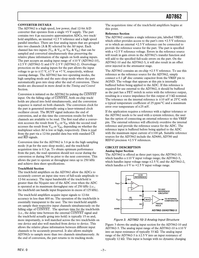
CIRCUIT DESCRIPTIONAnalog Input SectionThe AD7862 is offered as three part types; the AD7862-10,which handles a ±10 V input voltage range; the AD7862-3,which handles input voltage range ±2.5 V; and the AD7862-2,which handles a 0 V to +2.5 V input voltage range.
AGNDAD7862-10/AD7862-3
VAX
VREF
TRACK/HOLD
TO ADCREFERENCECIRCUITRY
TO INTERNALCOMPARATOR
R3
R2R1
MUX
2kΩ
+2.5VREFERENCE
Figure 3. AD7862-10/-3 Analog Input Structure
Figure 3 shows the analog input section for the AD7862-10 andAD7862-3. The analog input range of the AD7862-10 is ±10 Vinto an input resistance of typically 33 kΩ. The analog inputrange of the AD7862-3 is ±2.5 V into an input resistance oftypically 12 kΩ. This input is benign with no dynamic charging

AD7862
–8– REV. 0
currents, as the resistor stage is followed by a high inputimpedance stage of the track/hold amplifier. For the AD7862-10,R1 = 30 kΩ, R2 = 7.5 kΩ, and R3 = 10 kΩ. For the AD7862-3,R1 = R2 = 6.5 kΩ and R3 is open circuit.
For the AD7862-10 and AD7862-3, the designed code transi-tions occur on successive integer LSB values (i.e., 1 LSB,2 LSBs, 3 LSBs . . .). Output coding is twos complementbinary with 1 LSB = FS/4096. The ideal input/output transferfunction for the AD7862-10 and AD7862-3 is shown in Table I.
Table I. Ideal Input/Output Code Table for the AD7862-10/-3
Analog Inputl Digital Output Code Transition
+FSR/2 – 1 LSB2 011 . . . 110 to 011 . . . 111+FSR/2 – 2 LSBs 011 . . . 101 to 011 . . . 110+FSR/2 – 3 LSBs 011 . . . 100 to 011 . . . 101GND + 1 LSB 000 . . . 000 to 000 . . . 001GND 111 . . . 111 to 000 . . . 000GND – 1 LSB 111 . . . 110 to 111 . . . 111–FSR/2 + 3 LSBs 100 . . . 010 to 100 . . . 011–FSR/2 + 2 LSBs 100 . . . 001 to 100 . . . 010–FSR/2 + 1 LSB 100 . . . 000 to 100 . . . 001
NOTES1FSR is full-scale range = 20 V (AD7862-10) and = 5 V (AD7862-3) withREF IN = +2.5 V.
21 LSB = FSR/4096 = 4.883 mV (AD7862-10) and 1.22 mV (AD7862-3) withREF IN = +2.5 V.
The analog input section for the AD7862-2 contains no biasingresistors, and the VAX/BX pin drives the input to the multiplexerand track/hold amplifier circuitry directly. The analog inputrange is 0 V to +2.5 V into a high impedance stage with aninput current of less than 500 nA. This input is benign with nodynamic charging currents. Once again, the designed codetransitions occur on successive integer LSB values. Outputcoding is straight (natural) binary with 1 LSB = FS/4096 =2.5 V/4096 = 0.61 mV. Table II shows the ideal input/outputtransfer function for the AD7862-2.
Table II. Ideal Input/Output Code Table for the AD7862-2
Analog Input1 Digital Output Code Transition
+FSR – 1 LSB2 111 . . . 110 to 111 . . . 111+FSR – 2 LSB 111 . . . 101 to 111 . . . 110+FSR – 3 LSB 111 . . . 100 to 111 . . . 101GND + 3 LSB 000 . . . 010 to 000 . . . 011GND + 2 LSB 000 . . . 001 to 000 . . . 010GND + 1 LSB 000 . . . 000 to 000 . . . 001
NOTES1FSR is full-scale range and is 2.5 V for AD7862-2 with VREF = +2.5 V.21 LSB = FSR/4096 and is 0.61 mV for AD7862-2 with VREF = +2.5 V.
OFFSET AND FULL-SCALE ADJUSTMENTIn most digital signal processing (DSP) applications, offset andfull-scale errors have little or no effect on system performance.Offset error can always be eliminated in the analog domain byac coupling. Full-scale error effect is linear and does not causeproblems as long as the input signal is within the full dynamicrange of the ADC. Invariably, some applications will require theinput signal to span the full analog input dynamic range. In such
applications, offset and full-scale error will have to be adjustedto zero.
Figure 4 shows a circuit that can be used to adjust the offset andfull-scale errors on the AD7862 (VA1 on the AD7862-10 versionis shown for example purposes only). Where adjustment isrequired, offset error must be adjusted before full-scale error.This is achieved by trimming the offset of the op amp drivingthe analog input of the AD7862 while the input voltage is a1/2 LSB below analog ground. The trim procedure is as follows:apply a voltage of –2.44 mV (–1/2 LSB) at VA1 (see Figure 4)and adjust the op amp offset voltage until the ADC output codeflickers between 1111 1111 1111 and 0000 0000 0000.
V1
R110kΩ
R2500Ω
R310kΩ
AGND
AD7862*
*ADDITIONAL PINS OMITTED FOR CLARITY
INPUTRANGE = ±10V
10kΩR510kΩ
R4
VA1
Figure 4. Full-Scale Adjust Circuit
Gain error can be adjusted at either the first code transition(ADC negative full scale) or the last code transition (ADCpositive full scale). The trim procedures for both cases are asfollows:
Positive Full-Scale AdjustApply a voltage of +9.9927 V (FS/2 – 3/2 LSBs) at VA1. AdjustR2 until the ADC output code flickers between 0111 1111 1110and 0111 1111 1111.
Negative Full-Scale AdjustApply a voltage of –9.9976 V (–FS + 1/2 LSB) at VA1 and adjustR2 until the ADC output code flickers between 1000 0000 0000and 1000 0000 0001.
An alternative scheme for adjusting full-scale error in systemsthat use an external reference is to adjust the voltage at theVREF pin until the full-scale error for any of the channels isadjusted out. The good full-scale matching of the channels willensure small full-scale errors on the other channels.
TIMING AND CONTROLFigure 5a shows the timing and control sequence required toobtain optimum performance (Mode 1) from the AD7862. Inthe sequence shown, a conversion is initiated on the falling edgeof CONVST. This places both track/holds into hold simulta-neously, and new data from this conversion is available in theoutput register of the AD7862 3.6 µs later. The BUSY signalindicates the end of conversion, and at this time the conversionresults for both inputs are available to be read. A secondconversion is then initiated. If the multiplexer select A0 is low,the first and second read pulses after the first conversion accessesthe result from channel A (VA1 and VA2 respectively). The third
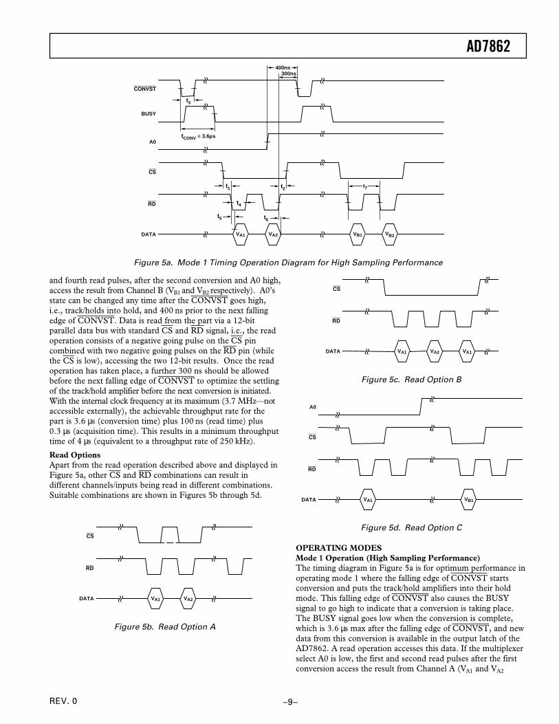
AD7862
–9–REV. 0
and fourth read pulses, after the second conversion and A0 high,access the result from Channel B (VB1 and VB2 respectively). A0’sstate can be changed any time after the CONVST goes high,i.e., track/holds into hold, and 400 ns prior to the next fallingedge of CONVST. Data is read from the part via a 12-bitparallel data bus with standard CS and RD signal, i.e., the readoperation consists of a negative going pulse on the CS pincombined with two negative going pulses on the RD pin (whilethe CS is low), accessing the two 12-bit results. Once the readoperation has taken place, a further 300 ns should be allowedbefore the next falling edge of CONVST to optimize the settlingof the track/hold amplifier before the next conversion is initiated.With the internal clock frequency at its maximum (3.7 MHz—notaccessible externally), the achievable throughput rate for thepart is 3.6 µs (conversion time) plus 100 ns (read time) plus0.3 µs (acquisition time). This results in a minimum throughputtime of 4 µs (equivalent to a throughput rate of 250 kHz).
Read OptionsApart from the read operation described above and displayed inFigure 5a, other CS and RD combinations can result indifferent channels/inputs being read in different combinations.Suitable combinations are shown in Figures 5b through 5d.
VA1 VA2
CS
RD
DATA
Figure 5b. Read Option A
VA1 VA2
CS
RD
DATA VA1
Figure 5c. Read Option B
VA1 VB1
A0
CS
RD
DATA
Figure 5d. Read Option C
OPERATING MODESMode 1 Operation (High Sampling Performance)The timing diagram in Figure 5a is for optimum performance inoperating mode 1 where the falling edge of CONVST startsconversion and puts the track/hold amplifiers into their holdmode. This falling edge of CONVST also causes the BUSYsignal to go high to indicate that a conversion is taking place.The BUSY signal goes low when the conversion is complete,which is 3.6 µs max after the falling edge of CONVST, and newdata from this conversion is available in the output latch of theAD7862. A read operation accesses this data. If the multiplexerselect A0 is low, the first and second read pulses after the firstconversion access the result from Channel A (VA1 and VA2
VA1 VA2 VB1 VB2
t3
t1 t2
t4
t5 t6
tCONV = 3.6µs
t7
CONVST
BUSY
A0
CS
RD
DATA
300ns400ns
Figure 5a. Mode 1 Timing Operation Diagram for High Sampling Performance
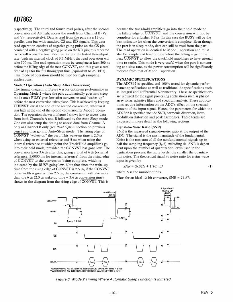
AD7862
–10– REV. 0
respectively). The third and fourth read pulses, after the secondconversion and A0 high, access the result from Channel B (VB1
and VB2 respectively). Data is read from the part via a 12-bitparallel data bus with standard CS and RD signals. This dataread operation consists of negative going pulse on the CS pincombined with a negative going pulse on the RD pin; this repeatedtwice will access the two 12-bit results. For the fastest throughputrate (with an internal clock of 3.7 MHz), the read operation willtake 100 ns. The read operation must be complete at least 300 nsbefore the falling edge of the next CONVST, and this gives a totaltime of 4 µs for the full throughput time (equivalent to 250 kHz).This mode of operation should be used for high samplingapplications.
Mode 2 Operation (Auto Sleep After Conversion)The timing diagram in Figure 6 is for optimum performance inOperating Mode 2 where the part automatically goes into sleepmode once BUSY goes low after conversion and “wakes-up”before the next conversion takes place. This is achieved by keepingCONVST low at the end of the second conversion, whereas itwas high at the end of the second conversion for Mode 1 opera-tion. The operation shown in Figure 6 shows how to access datafrom both Channels A and B followed by the Auto Sleep mode.One can also setup the timing to access data from Channel Aonly or Channel B only (see Read Options section on previouspage) and then go into Auto-Sleep mode. The rising edge ofCONVST “wakes-up” the part. This wake-up time is 2.5 µswhen using an external reference and 5 ms when using theinternal reference at which point the Track/Hold amplifier’s gointo their hold mode, provided the CONVST has gone low. Theconversion takes 3.6 µs after this, giving a total of 6 µs (externalreference, 5.0035 ms for internal reference) from the rising edgeof CONVST to the conversion being complete, which isindicated by the BUSY going low. Note that since the wake-uptime from the rising edge of CONVST is 2.5 µs, if the CONVSTpulse width is greater than 2.5 µs, the conversion will take morethan the 6 µs (2.5 µs wake-up time + 3.6 µs conversion time)shown in the diagram from the rising edge of CONVST. This is
because the track/hold amplifiers go into their hold mode onthe falling edge of CONVST, and the conversion will not becomplete for a further 3.6 µs. In this case the BUSY will be thebest indicator for when the conversion is complete. Even thoughthe part is in sleep mode, data can still be read from the part.The read operation is identical to Mode 1 operation and mustalso be complete at least 300 ns before the falling edge of thenext CONVST to allow the track/hold amplifiers to have enoughtime to settle. This mode is very useful when the part is convert-ing at a slow rate, as the power consumption will be significantlyreduced from that of Mode 1 operation.
DYNAMIC SPECIFICATIONSThe AD7862 is specified and 100% tested for dynamic perfor-mance specifications as well as traditional dc specifications suchas Integral and Differential Nonlinearity. These ac specificationsare required for the signal processing applications such as phasedarray sonar, adaptive filters and spectrum analysis. These applica-tions require information on the ADC’s effect on the spectralcontent of the input signal. Hence, the parameters for which theAD7862 is specified include SNR, harmonic distortion, inter-modulation distortion and peak harmonics. These terms arediscussed in more detail in the following sections.
Signal-to-Noise Ratio (SNR)SNR is the measured signal-to-noise ratio at the output of theADC. The signal is the rms magnitude of the fundamental.Noise is the rms sum of all the nonfundamental signals up tohalf the sampling frequency (fS/2) excluding dc. SNR is depen-dent upon the number of quantization levels used in thedigitization process; the more levels, the smaller the quantiza-tion noise. The theoretical signal to noise ratio for a sine waveinput is given by
SNR = (6.02N + 1.76) dB (1)
where N is the number of bits.
Thus for an ideal 12-bit converter, SNR = 74 dB.
VA1 VA2 VB1 VB2
t3
tCONV = 3.6µs
CONVST
BUSY
A0
CS
RD
DATA
300ns400ns
t3
2.5µs*/5ms**WAKE-UP
TIME
tCONV = 3.5µs
**WHEN USING AN EXTERNAL REFERENCE, WAKE-UP TIME = 2.5µs**WHEN USING AN INTERNAL REFERENCE, WAKE-UP TIME = 5ms
Figure 6. Mode 2 Timing Where Automatic Sleep Function Is Initiated

AD7862
–11–REV. 0
Figure 7 shows a histogram plot for 8192 conversions of a dcinput using the AD7862 with 5 V supply. The analog input wasset at the center of a code transition. It can be seen that all thecodes appear in the one output bin indicating very good noiseperformance from the ADC.
746 756747 748 749 750 751 752 753 754 755
9000
8000
0
4000
3000
2000
1000
6000
5000
7000
Figure 7. Histogram of 8192 Conversions of a DC Input
The same data is presented in Figure 8 as in Figure 7 exceptthat in this case the output data read for the device occursduring conversion. This has the effect of injecting noise onto thedie while bit decisions are being made and this increases thenoise generated by the AD7862. The histogram plot for 8192conversions of the same dc input now shows a larger spread ofcodes. This effect will vary depending on where the serial clockedges appear with respect to the bit trials of the conversionprocess. It is possible to achieve the same level of performancewhen reading during conversion as when reading after conver-sion depending on the relationship of the serial clock edges tothe bit trial points.
The output spectrum from the ADC is evaluated by applying asine wave signal of very low distortion to the VAX/BX input that issampled at a 245.76 kHz sampling rate. A Fast Fourier Trans-form (FFT) plot is generated from which the SNR data can beobtained. Figure 9 shows a typical 2048 point FFT plot of theAD7862 with an input signal of 10 kHz and a sampling fre-quency of 245.76 kHz. The SNR obtained from this graph is72.95 dB. It should be noted that the harmonics are taken intoaccount when calculating the SNR.
745 755746 747 748 749 750 751 752 753 7540
4000
3000
2000
1000
6000
5000
7000
Figure 8. Histogram of the 8192 Conversions with ReadDuring Conversion
–0
–1200 12.2k10k 30k 50k 70k 90k
–20
–40
–60
–80
–100
–10
–30
–50
–70
–90
–110
100k
FSAMPLE = 245760 FIN = 10kHz SNR = –72.95dB THD = –89.99dB
Figure 9. AD7862 FFT Plot
Effective Number of BitsThe formula given in Equation 1 relates the SNR to the numberof bits. Rewriting the formula, as in Equation 2, it is possible toget a measure of performance expressed in effective number ofbits (N).
N =
SNR −1.766.02
(2)
The effective number of bits for a device can be calculateddirectly from its measured SNR.
Figure 10 shows a typical plot of effective number of bits versusfrequency for an AD7862BN with a sampling frequency of245.76 kHz. The effective number of bits typically falls between11.6 and 10.6 corresponding to SNR figures of 71.59 dB and65.57 dB.
0 1000200 400 600 80010.2
11.4
11.2
11.0
10.8
11.8
11.6
12.0
10.6
10.4
FREQUENCY – kHz
EN
OB
Figure 10. Effective Numbers of Bits vs. Frequency
Total Harmonic Distortion (THD)Total Harmonic Distortion (THD) is the ratio of the rms sumof harmonics to the rms value of the fundamental. For theAD7862, THD is defined as
THD dB( ) = 20 log
V22 +V3
2 +V42 +V5
2
V1
where V1 is the rms amplitude of the fundamental and V2, V3,V4 and V5 are the rms amplitudes of the second through thesixth harmonic. The THD is also derived from the FFT plot ofthe ADC output spectrum.
AD7862
–12– REV. 0
Intermodulation DistortionWith inputs consisting of sine waves at two frequencies, fa andfb, any active device with nonlinearities will create distortionproducts at sum and difference frequencies of mfa ± nfb wherem, n = 0, 1, 2, 3 . . ., etc. Intermodulation terms are those forwhich neither m or n are equal to zero. For example, the secondorder terms include (fa + fb) and (fa – fb) while the third orderterms include (2 fa + fb), (2 fa – fb), (fa + 2 fb) and (fa – 2 fb).
Using the CCIF standard where two input frequencies near thetop end of the input bandwidth are used, the second and thirdorder terms are of different significance. The second order termsare usually distanced in frequency from the original sine waveswhile the third order terms are usually at a frequency close tothe input frequencies. As a result, the second and third orderterms are specified separately. The calculation of the inter-modulation distortion is as per the THD specification where it isthe ratio of the rms sum of the individual distortion products tothe rms amplitude of the fundamental expressed in dBs. In thiscase the input consists of two, equal amplitude, low distortionsine waves. Figure 11 shows a typical IMD plot for the AD7862.
–0
–1200 12.3k10k 30k 50k 70k 90k
–20
–40
–60
–80
–100
–10
–30
–50
–70
–90
–110
100k
INPUT FREQUENCIES F1 = 50010 Hz F2 = 49110 Hz FSAMPLE = 245760 Hz SNR = –60.62dB THD = –89.22dB
IMD: 2ND ORDER TERM –88.44 dB 3RD ORDER TERM –66.20 dB
Figure 11. AD7862 IMD Plot
Peak Harmonic or Spurious NoiseHarmonic or spurious noise is defined as the ratio of the rmsvalue of the next largest component in the ADC output spec-trum (up to fS/2 and excluding dc) to the rms value of thefundamental. Normally, the value of this specification will bedetermined by the largest harmonic in the spectrum, but forparts where the harmonics are buried in the noise floor, the peakwill be a noise peak.
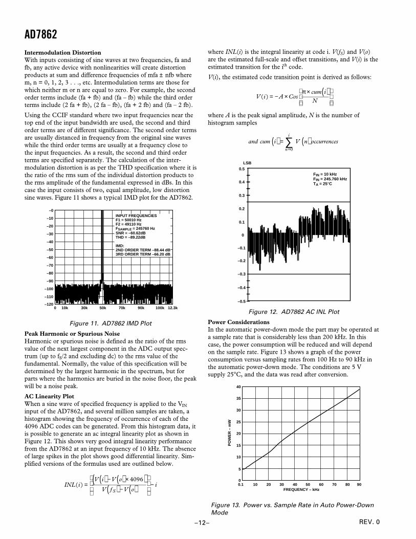
AC Linearity PlotWhen a sine wave of specified frequency is applied to the VIN
input of the AD7862, and several million samples are taken, ahistogram showing the frequency of occurrence of each of the4096 ADC codes can be generated. From this histogram data, itis possible to generate an ac integral linearity plot as shown inFigure 12. This shows very good integral linearity performancefrom the AD7862 at an input frequency of 10 kHz. The absenceof large spikes in the plot shows good differential linearity. Sim-plified versions of the formulas used are outlined below.
INL(i ) =V i( ) −V o( ) × 4096( )
V f S( ) −V o( )
− i
where INL(i) is the integral linearity at code i. V(fS) and V(o)are the estimated full-scale and offset transitions, and V(i) is theestimated transition for the ith code.
V(i), the estimated code transition point is derived as follows:
V (i ) = − A × Cosπ × cum i( )
N
where A is the peak signal amplitude, N is the number ofhistogram samples
and cum i( ) = V n( )n=0
i
∑ occurrences
0
–0.1
–0.2
–0.3
–0.4
–0.5
0.5
0.4
0.3
0.2
0.1
LSB
FIN = 10 kHzFIN = 245.760 kHzTA = 25°C
Figure 12. AD7862 AC INL Plot
Power ConsiderationsIn the automatic power-down mode the part may be operated ata sample rate that is considerably less than 200 kHz. In thiscase, the power consumption will be reduced and will dependon the sample rate. Figure 13 shows a graph of the powerconsumption versus sampling rates from 100 Hz to 90 kHz inthe automatic power-down mode. The conditions are 5 Vsupply 25°C, and the data was read after conversion.
0.1 9010 20 30 400
25
20
15
10
35
30
40
5
FREQUENCY – kHz
PO
WE
R –
mW
50 60 70 80
Figure 13. Power vs. Sample Rate in Auto Power-DownMode
AD7862
–13–REV. 0
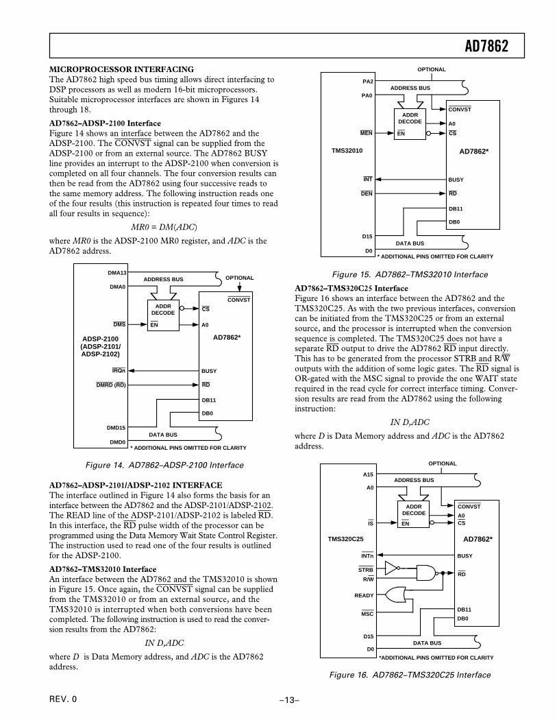
MICROPROCESSOR INTERFACINGThe AD7862 high speed bus timing allows direct interfacing toDSP processors as well as modern 16-bit microprocessors.Suitable microprocessor interfaces are shown in Figures 14through 18.
AD7862–ADSP-2100 InterfaceFigure 14 shows an interface between the AD7862 and theADSP-2100. The CONVST signal can be supplied from theADSP-2100 or from an external source. The AD7862 BUSYline provides an interrupt to the ADSP-2100 when conversion iscompleted on all four channels. The four conversion results canthen be read from the AD7862 using four successive reads tothe same memory address. The following instruction reads oneof the four results (this instruction is repeated four times to readall four results in sequence):
MR0 = DM(ADC)
where MR0 is the ADSP-2100 MR0 register, and ADC is theAD7862 address.
OPTIONAL
DMA0
DMA13
DMD15
DMD0
DMS EN
ADDRDECODE
ADDRESS BUS
ADSP-2100(ADSP-2101/ADSP-2102)
* ADDITIONAL PINS OMITTED FOR CLARITY
DATA BUS
CONVST
CS
DB11
DB0
RD
BUSY
AD7862*
IRQn
DMRD (RD)
A0
Figure 14. AD7862–ADSP-2100 Interface
AD7862–ADSP-2101/ADSP-2102 INTERFACEThe interface outlined in Figure 14 also forms the basis for aninterface between the AD7862 and the ADSP-2101/ADSP-2102.The READ line of the ADSP-2101/ADSP-2102 is labeled RD.In this interface, the RD pulse width of the processor can beprogrammed using the Data Memory Wait State Control Register.The instruction used to read one of the four results is outlinedfor the ADSP-2100.
AD7862–TMS32010 InterfaceAn interface between the AD7862 and the TMS32010 is shownin Figure 15. Once again, the CONVST signal can be suppliedfrom the TMS32010 or from an external source, and theTMS32010 is interrupted when both conversions have beencompleted. The following instruction is used to read the conver-sion results from the AD7862:
IN D,ADC
where D is Data Memory address, and ADC is the AD7862address.
OPTIONAL
PA0
PA2
D15
D0
MEN EN
ADDRDECODE
ADDRESS BUS
TMS32010
* ADDITIONAL PINS OMITTED FOR CLARITY
DATA BUS
CONVST
CS
DB11
DB0
RD
BUSY
AD7862*
INT
DEN
A0
Figure 15. AD7862–TMS32010 Interface
AD7862–TMS320C25 InterfaceFigure 16 shows an interface between the AD7862 and theTMS320C25. As with the two previous interfaces, conversioncan be initiated from the TMS320C25 or from an externalsource, and the processor is interrupted when the conversionsequence is completed. The TMS320C25 does not have aseparate RD output to drive the AD7862 RD input directly.This has to be generated from the processor STRB and R/Woutputs with the addition of some logic gates. The RD signal isOR-gated with the MSC signal to provide the one WAIT staterequired in the read cycle for correct interface timing. Conver-sion results are read from the AD7862 using the followinginstruction:
IN D,ADC
where D is Data Memory address and ADC is the AD7862address.
A0
A15
D15
D0
IS EN
ADDRDECODE
ADDRESS BUS
OPTIONAL
DATA BUS
CONVST
CS
DB11
DB0
RD
BUSY
AD7862*TMS320C25
*ADDITIONAL PINS OMITTED FOR CLARITY
INTn
R/W
STRB
MSC
READY
A0
Figure 16. AD7862–TMS320C25 Interface

AD7862
–14– REV. 0
Some applications may require that the conversion be initiatedby the microprocessor rather than an external timer. One optionis to decode the AD7862 CONVST from the address bus sothat a write operation starts a conversion. Data is read at theend of the conversion sequence as before. Figure 18 shows anexample of initiating conversion using this method. Note thatfor all interfaces, it is preferred that a read operation not beattempted during conversion.
AD7862–MC68000 InterfaceAn interface between the AD7862 and the MC68000 is shownin Figure 17. As before, conversion can be supplied from theMC68000 or from an external source. The AD7862 BUSY linecan be used to interrupt the processor or, alternatively, softwaredelays can ensure that conversion has been completed before aread to the AD7862 is attempted. Because of the nature of itsinterrupts, the 68000 requires additional logic (not shown inFigure 18) to allow it to be interrupted correctly. For furtherinformation on 68000 interrupts, consult the 68000 user’s manual.
The MC68000 AS and R/W outputs are used to generate aseparate RD input signal for the AD7862. CS is used to drivethe 68000 DTACK input to allow the processor to execute anormal read operation to the AD7862. The conversion resultsare read using the following 68000 instruction:
MOVE.W ADC,D0
where D0 is the 68000 D0 register, and ADC is the AD7862address.
A0
A15
D15
D0
EN
ADDRDECODE
ADDRESS BUS
OPTIONAL
DATA BUS
CONVST
CS
DB11
DB0
RD
AD7862*
MC68000
*ADDITIONAL PINS OMITTED FOR CLARITY
DTACK
R/W
AS
A0
Figure 17. AD7862–MC68000 Interface
AD7862–80C196 InterfaceFigure 18 shows an interface between the AD7862 and the80C196 microprocessor. Here, the microprocessor initiatesconversion. This is achieved by gating the 80C196 WR signalwith a decoded address output (different to the AD7862 CSaddress). The AD7862 BUSY line is used to interrupt themicroprocessor when the conversion sequence is completed.
D15
D0
ADDRDECODE
ADDRESS BUS
ADDRESS/DATA BUS
CONVST
CS
DB11
DB0
RD
AD7862*
80C196
*ADDITIONAL PINS OMITTED FOR CLARITY
WR
RD
A0
A15
A1
Figure 18. AD7862–8086 Interface
Vector Motor ControlThe current drawn by a motor can be split into two compo-nents: one produces torque, and the other produces magneticflux. For optimal performance of the motor, these two compo-nents should be controlled independently. In conventionalmethods of controlling a three-phase motor, the current (orvoltage) supplied to the motor and the frequency of the drive arethe basic control variables; however, both the torque and fluxare functions of current (or voltage) and frequency. Thiscoupling effect can reduce the performance of the motorbecause, if the torque is increased by increasing the frequency,for example, the flux tends to decrease.
Vector control of an ac motor involves controlling phase inaddition to drive and current frequency. Controlling the phaseof the motor requires feedback information on the position ofthe rotor relative to the rotating magnetic field in the motor.Using this information, a vector controller mathematicallytransforms the three phase drive currents into separate torqueand flux components. The AD7862, with its four-channelsimultaneous sampling capability, is ideally suited for use invector motor control applications.
A block diagram of a vector motor control application using theAD7862 is shown in Figure 19. The position of the field isderived by determining the current in each phase of the motor.Only two phase currents need to be measured because the thirdcan be calculated if two phases are known. VA1 and VA2 of theAD7862 are used to digitize this information.
Simultaneous sampling is critical to maintain the relative phaseinformation between the two channels. A current sensingisolation amplifier, transformer or Hall effect sensor is usedbetween the motor and the AD7862. Rotor information isobtained by measuring the voltage from two of the inputs to themotor. VB1 and VB2 of the AD7862 are used to obtain thisinformation. Once again, the relative phase of the two channelsis important. A DSP microprocessor is used to perform themathematical transformations and control loop calculations onthe information fed back by the AD7862.
AD7862
–15–REV. 0
VOLTAGEATTENUATORS
DAC
DAC
DACTORQUE
SETPOINT
A1V
VB2
VB1
VA2
*ADDITIONAL PINS OMITTED FOR CLARITY
TORQUE & FLUXCONTROL LOOP
CALCULATIONS &TWO TO THREE
PHASEINFORMATION
TRANSFORMATIONTO TORQUE &
FLUX CURRENTCOMPONENTS
FLUXSETPOINT
DRIVECIRCUITRY
ISOLATIONAMPLIFIERS
AD7862*
DSPMICROPROCESSOR
IC
IB
IA
VB
VA
3PHASEMOTOR
Figure 19. Vector Motor Control Using the AD7862
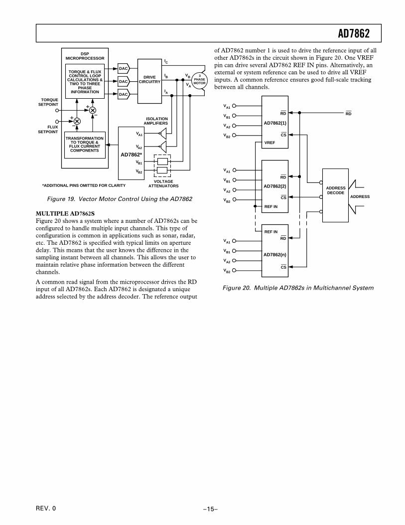
MULTIPLE AD7862SFigure 20 shows a system where a number of AD7862s can beconfigured to handle multiple input channels. This type ofconfiguration is common in applications such as sonar, radar,etc. The AD7862 is specified with typical limits on aperturedelay. This means that the user knows the difference in thesampling instant between all channels. This allows the user tomaintain relative phase information between the differentchannels.
A common read signal from the microprocessor drives the RDinput of all AD7862s. Each AD7862 is designated a uniqueaddress selected by the address decoder. The reference output
of AD7862 number 1 is used to drive the reference input of allother AD7862s in the circuit shown in Figure 20. One VREFpin can drive several AD7862 REF IN pins. Alternatively, anexternal or system reference can be used to drive all VREFinputs. A common reference ensures good full-scale trackingbetween all channels.
AD7862(1)
AD7862(2)
AD7862(n)
CS
RD
CS
RD
CS
RD RD
ADDRESS
VREF
REF IN
REF IN
ADDRESSDECODE
VA1
VB1
VA2
VB2
VA1
VB1
VA2
VB2
VA1
VB1
VA2
VB2
Figure 20. Multiple AD7862s in Multichannel System
AD7862
–16– REV. 0
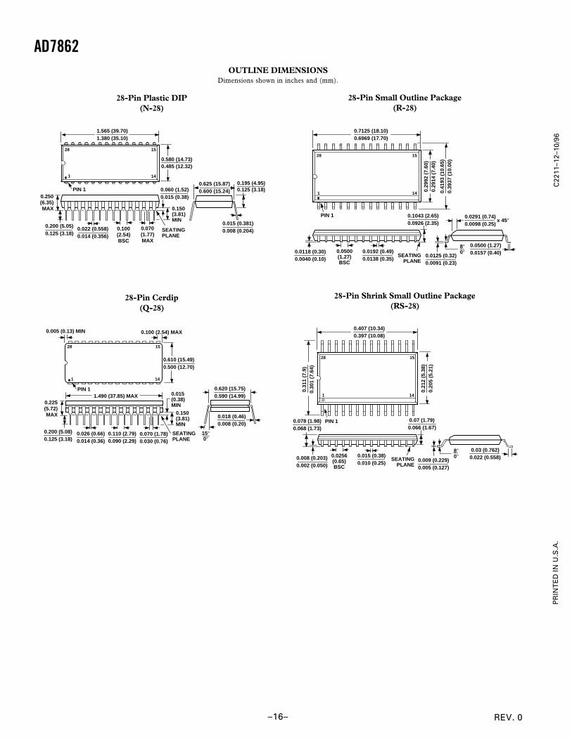
OUTLINE DIMENSIONSDimensions shown in inches and (mm).
C22
11–1
2–10
/96
PR
INT
ED
IN U
.S.A
.
28-Pin Plastic DIP(N-28)
28
1 14
15
1.565 (39.70)1.380 (35.10)
0.580 (14.73)0.485 (12.32)
PIN 1
0.022 (0.558)0.014 (0.356)
0.060 (1.52)0.015 (0.38)
0.200 (5.05)0.125 (3.18)
0.150(3.81)MIN
SEATINGPLANE
0.250(6.35)MAX
0.100(2.54)BSC
0.070(1.77)MAX
0.015 (0.381)0.008 (0.204)
0.195 (4.95)0.125 (3.18)
0.625 (15.87)0.600 (15.24)
28-Pin Cerdip(Q-28)
28
1 14
15
0.610 (15.49)0.500 (12.70)
PIN 1
0.005 (0.13) MIN 0.100 (2.54) MAX
15°0°
0.620 (15.75)0.590 (14.99)
0.018 (0.46)0.008 (0.20)
SEATINGPLANE
0.225(5.72)MAX
1.490 (37.85) MAX
0.150(3.81)MIN
0.200 (5.08)0.125 (3.18)
0.015(0.38)MIN
0.026 (0.66)0.014 (0.36)
0.110 (2.79)0.090 (2.29)
0.070 (1.78)0.030 (0.76)
28-Pin Small Outline Package(R-28)
SEATINGPLANE
0.0118 (0.30)0.0040 (0.10)
0.0192 (0.49)0.0138 (0.35)
0.1043 (2.65)0.0926 (2.35)
0.0500(1.27)BSC
0.0125 (0.32)0.0091 (0.23)
0.0500 (1.27)0.0157 (0.40)
8°0°
0.0291 (0.74)0.0098 (0.25)
x 45°
0.7125 (18.10)0.6969 (17.70)
0.41
93 (
10.6
5)0.
3937
(10
.00)
0.29
92 (
7.60
)0.
2914
(7.
40)
PIN 1
28 15
141
28-Pin Shrink Small Outline Package(RS-28)
28 15
141
0.407 (10.34)0.397 (10.08)
0.31
1 (7
.9)
0.30
1 (7
.64)
0.21
2 (5
.38)
0.20
5 (5
.21)
PIN 1
SEATINGPLANE
0.008 (0.203)0.002 (0.050)
0.07 (1.79)0.066 (1.67)
0.0256(0.65)BSC
0.078 (1.98)0.068 (1.73)
0.015 (0.38)0.010 (0.25) 0.009 (0.229)
0.005 (0.127)
0.03 (0.762)0.022 (0.558)
8°0°