ad5520 per pin parametric measurement unit/source measure ... · source measure, parametric...
TRANSCRIPT
Per Pin ParametricMeasurement Unit/Source Measure Unit
AD5520
Rev. B Information furnished by Analog Devices is believed to be accurate and reliable. However, no responsibility is assumed by Analog Devices for its use, nor for any infringements of patents or other rights of third parties that may result from its use. Specifications subject to change without notice. No license is granted by implication or otherwise under any patent or patent rights of Analog Devices. Trademarks and registered trademarks are the property of their respective owners.
One Technology Way, P.O. Box 9106, Norwood, MA 02062-9106, U.S.A.Tel: 781.329.4700 www.analog.com Fax: 781.461.3113 © 2005 Analog Devices, Inc. All rights reserved.
FEATURES Force/measure functions
FIMV, FVMI, FVMV, FIMI, FNMV Force/measure voltage range ±11 V 4 user programmable force/measure current ranges
±4 μA, ±40 μA, ±400 μA, ±4 mA (external resistors) 2 user programmable extended current ranges
Up to 6 mA without external driver Higher currents with external driver
Clamp circuitry and window comparators on board Guard amplifier 64-lead LQFP package
APPLICATIONS Automatic test equipment
Per pin PMU, shared pin PMU, device power supply instrumentation
Source measure, parametric measurement, precision measurement
GENERAL DESCRIPTION
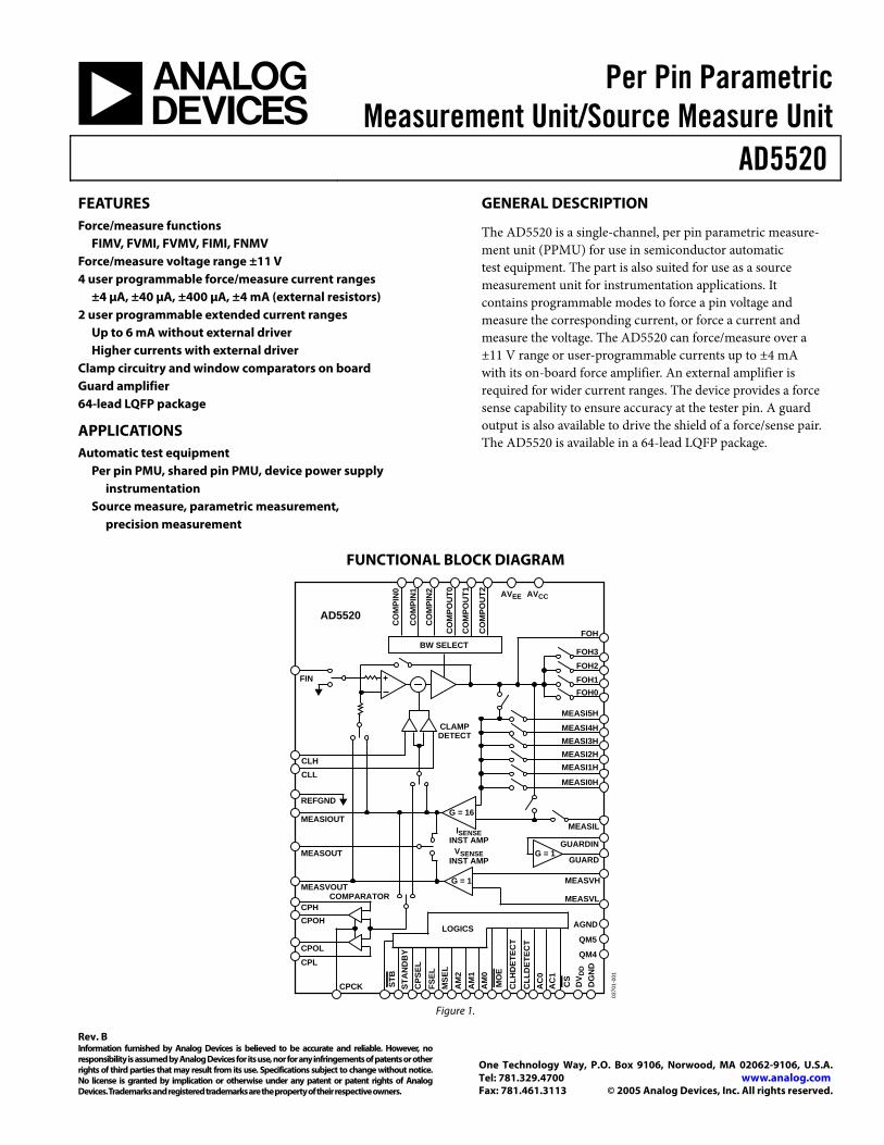
The AD5520 is a single-channel, per pin parametric measure-ment unit (PPMU) for use in semiconductor automatic test equipment. The part is also suited for use as a source measurement unit for instrumentation applications. It contains programmable modes to force a pin voltage and measure the corresponding current, or force a current and measure the voltage. The AD5520 can force/measure over a ±11 V range or user-programmable currents up to ±4 mA with its on-board force amplifier. An external amplifier is required for wider current ranges. The device provides a force sense capability to ensure accuracy at the tester pin. A guard output is also available to drive the shield of a force/sense pair. The AD5520 is available in a 64-lead LQFP package.
FUNCTIONAL BLOCK DIAGRAM
CLL
DET
ECT
MEASI4H
FIN
BW SELECT
CO
MPO
UT2
FOH1FOH2FOH3
FOH0
AVEE AVCC
CLHCLL
REFGND
MEASIOUT
MEASOUT
MEASVOUT
G = 16
G = 1
CPHCPOH
CPOLCPL
MEASI5H
MEASIL
GUARDIN
GUARD
MEASVH
MEASVL
AGND
QM5
QM4
DG
ND
DV D
D
CS
STA
ND
BY
CO
MPO
UT1
CO
MPO
UT0
CO
MPI
N2
CO
MPI
N1
CO
MPI
N0
CLAMPDETECT
ISENSEINST AMP
VSENSEINST AMP
LOGICS
AC
0A
C1
CLH
DET
ECT
MO
E
AM
0A
M1
AM
2M
SEL
FSEL
CPS
EL
STB
CPCK
AD5520
COMPARATOR
G = 1
FOH
MEASI3HMEASI2HMEASI1H
MEASI0H
0370
1-00
1
Figure 1.
AD5520
Rev. B | Page 2 of 24
TABLE OF CONTENTS Features .............................................................................................. 1
Applications....................................................................................... 1
General Description ......................................................................... 1
Functional Block Diagram .............................................................. 1
Specifications..................................................................................... 3
Timing Characteristics..................................................................... 6
Absolute Maximum Ratings............................................................ 7
ESD Caution.................................................................................. 7
Pin Configuration and Function Descriptions............................. 8
Typical Performance Characteristics ........................................... 10
Theory of Operation ...................................................................... 13
Interface ........................................................................................... 14
Standby Mode ............................................................................. 14
Force Voltage or Force Current ................................................ 14
Measured Parameter .................................................................. 14
Current Ranges ........................................................................... 14
RS Selection.................................................................................. 14
Force Control Amplifier ............................................................ 15
Comparator Function and Strobing ........................................ 15
Clamp Function.......................................................................... 15
High Current Ranges ................................................................. 15
Circuit Operation ........................................................................... 16
Force Voltage............................................................................... 16
Measure Current......................................................................... 16
Force Current.............................................................................. 17
Measure Voltage ......................................................................... 17
Short Circuit Protection ............................................................ 17
Settling Time Considerations ....................................................... 18
PCB Layout and Power Supply Decoupling................................ 19
Typical Connection Circuit for the AD5520 .............................. 20
Typical Application Circuit ........................................................... 21
Evaluation Board for the AD5520................................................ 22
Outline Dimensions ....................................................................... 24
Ordering Guide .......................................................................... 24
REVISION HISTORY
9/05—Rev. A to Rev. B Updated Format..................................................................Universal Changes to Features.......................................................................... 1 Changes to Figure 1.......................................................................... 1 Changes to Specifications ................................................................ 3 Changes to Force Current Section................................................ 17 Changes to Figure 26 ..................................................................... 20 Updated Outline Dimensions ....................................................... 24 Changes to Ordering Guide .......................................................... 24
10/03—Rev. 0 to Rev. A Changes to Specifications.................................................................3 Updated Ordering Guide .................................................................5
9/03—Revision 0: Initial Version
AD5520
Rev. B | Page 3 of 24
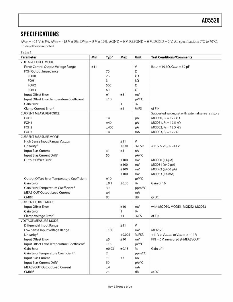
SPECIFICATIONS AVCC = +15 V ± 5%, AVEE = −15 V ± 5%, DVDD = 5 V ± 10%, AGND = 0 V, REFGND = 0 V, DGND = 0 V. All specifications 0°C to 70°C, unless otherwise noted.
Table 1. Parameter Min Typ1 Max Unit Test Conditions/Comments VOLTAGE FORCE MODE
Force Control Output Voltage Range ±11 V RLOAD = 10 kΩ, CLOAD = 50 pF FOH Output Impedance 70 Ω
FOH0 2.5 kΩ FOH1 3 kΩ FOH2 500 Ω FOH3 60 Ω
Input Offset Error ±1 ±5 mV Input Offset Error Temperature Coefficient ±10 μV/°C Gain Error 1 % Clamp Current Error2 ±1 % FS of FIN
CURRENT MEASURE/FORCE Suggested values; set with external sense resistors FOH0 ±4 μA MODE0, RS = 125 kΩ FOH1 ±40 μA MODE1, RS = 12.5 kΩ FOH2 ±400 μA MODE2, RS = 12.5 kΩ FOH3 ±4 mA MODE3, RS = 125 Ω
CURRENT MEASURE MODE High Sense Input Range, VMEASIxH ±11 V Linearity3 ±0.01 % FSR +11 V > VFOL > −11 V Input Bias Current ±1 ±3 nA Input Bias Current Drift1 50 pA/°C Output Offset Error ±100 mV MODE0 (±4 μA) ±100 mV MODE1 (±40 μA) ±100 mV MODE2 (±400 μA) ±100 mV MODE3 (±4 mA) Output Offset Error Temperature Coefficient ±10 μV/°C Gain Error ±0.1 ±0.35 % Gain of 16 Gain Error Temperature Coefficient4 30 ppm/°C MEASIOUT Output Load Current ±4 mA CMRR 95 dB @ DC
CURRENT FORCE MODE Input Offset Error ±10 mV with MODE0, MODE1, MODE2, MODE3 Gain Error 1 % Clamp Voltage Error2 ±1 % FS of FIN
VOLTAGE MEASURE MODE Differential Input Range ±11 V Low Sense Input Voltage Range ±100 mV MEASVL Linearity3 +0.005 % FSR +11 V > VMEASVH to VMEASVL > −11 V Input Offset Error ±5 ±10 mV FIN = 0 V, measured @ MEASVOUT Input Offset Error Temperature Coefficient1 ±15 μV/°C Gain Error ±0.03 ±0.15 % Gain of 1 Gain Error Temperature Coefficient4 2 ppm/°C Input Bias Current ±1 ±3 nA Input Bias Current Drift4 50 pA/°C MEASVOUT Output Load Current ±4 mA CMRR4 73 dB @ DC
AD5520
Rev. B | Page 4 of 24
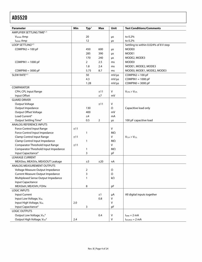
Parameter Min Typ1 Max Unit Test Conditions/Comments AMPLIFIER SETTLING TIME4, 5
VSENSE Amp 20 μs to 0.2% ISENSE Amp 12 μs to 0.2%
LOOP SETTLING4, 5 Settling to within 0.024% of 8 V step
COMPIN2 = 100 pF 450 600 μs MODE0
285 390 μs MODE1
170 240 μs MODE2, MODE3
COMPIN1 = 1000 pF 2 2.5 ms MODE0
1.8 2.4 ms MODE1, MODE2, MODE3
COMPIN0 = 3000 pF 5.75 8.7 ms MODE0, MODE1, MODE2, MODE3
SLEW RATE4, 5 50 mV/μs COMPIN2 = 100 pF 4.3 mV/μs COMPIN1 = 1000 pF 1.28 mV/μs COMPIN0 = 3000 pF
COMPARATOR CPH, CPL Input Range ±11 V VCPH > VCPL
Input Offset ±7 mV GUARD DRIVER
Output Voltage ±11 V Output Impedance 130 Ω Capacitive load only Output Offset Voltage 400 mV Load Current4 ±4 mA Output Settling Time4 0.5 2 μs 100 pF capacitive load
ANALOG REFERENCE INPUTS Force Control Input Range ±11 V Force Control Input Impedance 1 MΩ Clamp Control Input Range ±11 V VCLH > VCLL
Clamp Control Input Impedance 1 MΩ Comparator Threshold Input Range ±11 V Comparator Threshold Input Impedance 1 MΩ Input Capacitance4 3 pF
LEAKAGE CURRENT MEASIxx, MEASVx, MEASOUT Leakage ±3 ±20 nA
ANALOG MEASUREMENT OUTPUTS Voltage Measure Output Impedance 2 Ω Current Measure Output Impedance 3 Ω Multiplexed Sense Output Impedance 1 kΩ Input Capacitance MEASIxH, MEASVH, FOHx 8 pF
LOGIC INPUTS Input Current ±1 μA All digital inputs together Input Low Voltage, VINL 0.8 V Input High Voltage, VIHL 2.0 V Input Capacitance4 3 pF
LOGIC OUTPUTS Output Low Voltage, VOL
4 0.4 V ISINK = 2 mA Output High Voltage, VOH
4 2.4 V ISOURCE = 2 mA
AD5520
Rev. B | Page 5 of 24
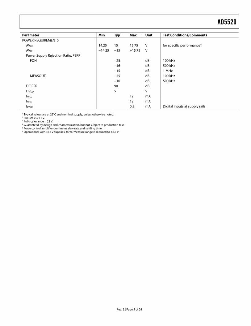
Parameter Min Typ1 Max Unit Test Conditions/Comments POWER REQUIREMENTS
AVCC 14.25 15 15.75 V for specific performance6
AVEE −14.25 −15 +15.75 V Power Supply Rejection Ratio, PSRR1
FOH −25 dB 100 kHz −16 dB 500 kHz −15 dB 1 MHz
MEASOUT −55 dB 100 kHz −10 dB 500 kHz DC PSR 90 dB DVDD 5 V IAVCC 12 mA IAVEE 12 mA IDVDD 0.5 mA Digital inputs at supply rails
1 Typical values are at 25°C and nominal supply, unless otherwise noted. 2 Full-scale = 11 V. 3 Full-scale range = 22 V. 4 Guaranteed by design and characterization, but not subject to production test. 5 Force control amplifier dominates slew rate and settling time. 6 Operational with ±12 V supplies, force/measure range is reduced to ±8.5 V.
AD5520
Rev. B | Page 6 of 24
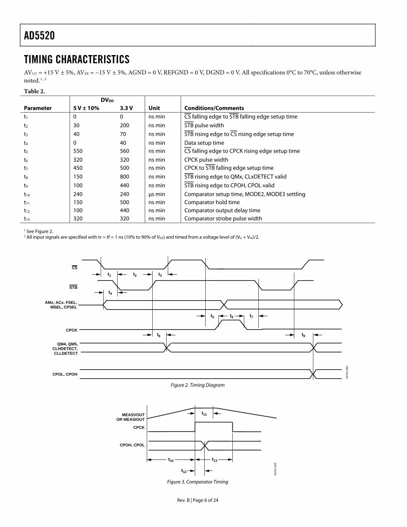
TIMING CHARACTERISTICS AVCC = +15 V ± 5%, AVEE = −15 V ± 5%, AGND = 0 V, REFGND = 0 V, DGND = 0 V. All specifications 0°C to 70°C, unless otherwise noted.1, 2
Table 2. DVDD Parameter 5 V ± 10% 3.3 V Unit Conditions/Comments t1 0 0 ns min CS falling edge to STB falling edge setup time
t2 30 200 ns min STB pulse width
t3 40 70 ns min STB rising edge to CS rising edge setup time
t4 0 40 ns min Data setup time t5 550 560 ns min CS falling edge to CPCK rising edge setup time
t6 320 320 ns min CPCK pulse width t7 450 500 ns min CPCK to STB falling edge setup time
t8 150 800 ns min STB rising edge to QMx, CLxDETECT valid
t9 100 440 ns min STB rising edge to CPOH, CPOL valid
t10 240 240 μs min Comparator setup time, MODE2, MODE3 settling t11 150 500 ns min Comparator hold time t12 100 440 ns min Comparator output delay time t13 320 320 ns min Comparator strobe pulse width 1 See Figure 2. 2 All input signals are specified with tr = tf = 1 ns (10% to 90% of VDD) and timed from a voltage level of (VIL + VIH)/2.
CPCK
AMx, ACx, FSEL,MSEL, CPSEL
CS
QM4, QM5,CLHDETECT,CLLDETECT
CPOL, CPOH
STB
t2t1 t3
t6t5 t7
t4
t6 t9
0370
1-00
2
Figure 2. Timing Diagram
CPCK
CPOH, CPOL
MEASVOUTOR MEASIOUT
t11
t12
t10 t13
0370
1-00
3
Figure 3. Comparator Timing
AD5520
Rev. B | Page 7 of 24
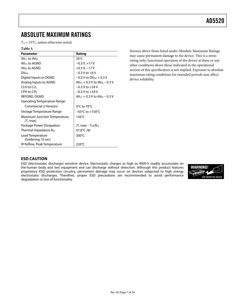
ABSOLUTE MAXIMUM RATINGS TA = 25°C, unless otherwise noted.
Table 3. Parameter Rating AVCC to AVEE 34 V AVCC to AGND −0.3 V, +17 V AVEE to AGND +0.3 V, −17 V DVDD −0.3 V to +6 V Digital Inputs to DGND −0.3 V to DVDD + 0.3 V Analog Inputs to AGND AVCC + 0.3 V to AVEE – 0.3 V CLH to CLL −0.3 V to +34 V CPH to CPL −0.3 V to +34 V REFGND, DGND AVCC + 0.3 V to AVEE – 0.3 V Operating Temperature Range
Commercial (J Version) 0°C to 70°C Storage Temperature Range −65°C to +150°C Maximum Junction Temperature,
(TJ max) 150°C
Package Power Dissipation (TJ max – TA)/θJA
Thermal Impedance θJA 47.8°C /W Lead Temperature
(Soldering 10 sec) 300°C
IR Reflow, Peak Temperature 220°C
Stresses above those listed under Absolute Maximum Ratings may cause permanent damage to the device. This is a stress rating only; functional operation of the device at these or any other conditions above those indicated in the operational section of this specification is not implied. Exposure to absolute maximum rating conditions for extended periods may affect device reliability.
ESD CAUTION ESD (electrostatic discharge) sensitive device. Electrostatic charges as high as 4000 V readily accumulate on the human body and test equipment and can discharge without detection. Although this product features proprietary ESD protection circuitry, permanent damage may occur on devices subjected to high energy electrostatic discharges. Therefore, proper ESD precautions are recommended to avoid performance degradation or loss of functionality.
AD5520
Rev. B | Page 8 of 24
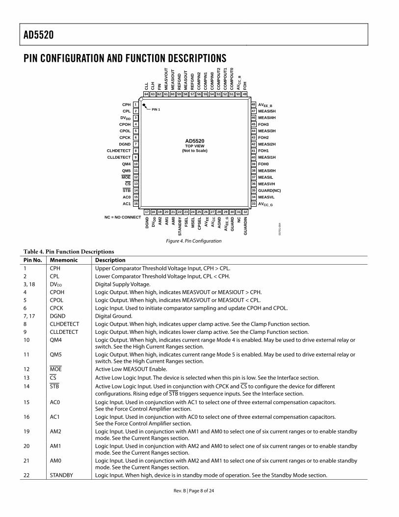
PIN CONFIGURATION AND FUNCTION DESCRIPTIONS
64
CLL
63
CLH
62
FIN
61
MEA
SVO
UT
60
MEA
SIO
UT
59
REF
GN
D
58
MEA
SOU
T
57
REF
GN
D
56
CO
MPI
N2
55
CO
MPI
N1
54
CO
MPI
N0
53
CO
MPO
UT2
52
CO
MPO
UT1
51
CO
MPO
UT0
50
AV C
C_B
49
FOH
47 MEASI5H46 MEASI4H45 FOH3
42 MEASI2H
43 FOH2
44 MEASI3H
48 AVEE_B
41 FOH140 MEASI1H39 FOH0
37 MEASIL36 MEASVH35 GUARD(NC)34 MEASVL33 AVCC_G
38 MEASI0H
2CPL3DVDD4CPOH
7DGND
6CPCK
5CPOL
1CPH
8CLHDETECT9CLLDETECT10QM4
12MOE13CS14STB15AC016AC1
11QM5
NC = NO CONNECT17
DG
ND
18
DV D
D
19
AM
2
20
AM
1
21
AM
0
22
STA
ND
BY
23
FSEL
24
MSE
L
25
CPS
EL
26
AV E
E27
AV C
C28
AG
ND
29
AV E
E_G
30
GU
AR
D
31
NC
32
GU
AR
DIN
PIN 1
AD5520TOP VIEW
(Not to Scale)
0370
1-00
4
Figure 4. Pin Configuration
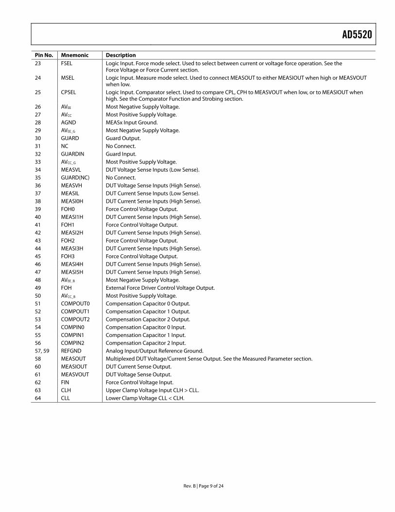
Table 4. Pin Function Descriptions Pin No. Mnemonic Description 1 CPH Upper Comparator Threshold Voltage Input, CPH > CPL. 2 CPL Lower Comparator Threshold Voltage Input, CPL < CPH. 3, 18 DVDD Digital Supply Voltage. 4 CPOH Logic Output. When high, indicates MEASVOUT or MEASIOUT > CPH. 5 CPOL Logic Output. When high, indicates MEASVOUT or MEASIOUT < CPL. 6 CPCK Logic Input. Used to initiate comparator sampling and update CPOH and CPOL. 7, 17 DGND Digital Ground. 8 CLHDETECT Logic Output. When high, indicates upper clamp active. See the Clamp Function section. 9 CLLDETECT Logic Output. When high, indicates lower clamp active. See the Clamp Function section. 10 QM4 Logic Output. When high, indicates current range Mode 4 is enabled. May be used to drive external relay or
switch. See the High Current Ranges section. 11 QM5 Logic Output. When high, indicates current range Mode 5 is enabled. May be used to drive external relay or
switch. See the High Current Ranges section. 12 MOE Active Low MEASOUT Enable.
13 CS Active Low Logic Input. The device is selected when this pin is low. See the Interface section.
14 STB Active Low Logic Input. Used in conjunction with CPCK and CS to configure the device for different configurations. Rising edge of STB triggers sequence inputs. See the Interface section.
15 AC0 Logic Input. Used in conjunction with AC1 to select one of three external compensation capacitors. See the Force Control Amplifier section.
16 AC1 Logic Input. Used in conjunction with AC0 to select one of three external compensation capacitors. See the Force Control Amplifier section.
19 AM2 Logic Input. Used in conjunction with AM1 and AM0 to select one of six current ranges or to enable standby mode. See the Current Ranges section.
20 AM1 Logic Input. Used in conjunction with AM2 and AM0 to select one of six current ranges or to enable standby mode. See the Current Ranges section.
21 AM0 Logic Input. Used in conjunction with AM2 and AM1 to select one of six current ranges or to enable standby mode. See the Current Ranges section.
22 STANDBY Logic Input. When high, device is in standby mode of operation. See the Standby Mode section.
AD5520
Rev. B | Page 9 of 24
Pin No. Mnemonic Description 23 FSEL Logic Input. Force mode select. Used to select between current or voltage force operation. See the
Force Voltage or Force Current section. 24 MSEL Logic Input. Measure mode select. Used to connect MEASOUT to either MEASIOUT when high or MEASVOUT
when low. 25 CPSEL Logic Input. Comparator select. Used to compare CPL, CPH to MEASVOUT when low, or to MEASIOUT when
high. See the Comparator Function and Strobing section. 26 AVEE Most Negative Supply Voltage. 27 AVCC Most Positive Supply Voltage. 28 AGND MEASx Input Ground. 29 AVEE_G Most Negative Supply Voltage. 30 GUARD Guard Output. 31 NC No Connect. 32 GUARDIN Guard Input. 33 AVCC_G Most Positive Supply Voltage. 34 MEASVL DUT Voltage Sense Inputs (Low Sense). 35 GUARD(NC) No Connect. 36 MEASVH DUT Voltage Sense Inputs (High Sense). 37 MEASIL DUT Current Sense Inputs (Low Sense). 38 MEASI0H DUT Current Sense Inputs (High Sense). 39 FOH0 Force Control Voltage Output. 40 MEASI1H DUT Current Sense Inputs (High Sense). 41 FOH1 Force Control Voltage Output. 42 MEASI2H DUT Current Sense Inputs (High Sense). 43 FOH2 Force Control Voltage Output. 44 MEASI3H DUT Current Sense Inputs (High Sense). 45 FOH3 Force Control Voltage Output. 46 MEASI4H DUT Current Sense Inputs (High Sense). 47 MEASI5H DUT Current Sense Inputs (High Sense). 48 AVEE_B Most Negative Supply Voltage. 49 FOH External Force Driver Control Voltage Output. 50 AVCC_B Most Positive Supply Voltage. 51 COMPOUT0 Compensation Capacitor 0 Output. 52 COMPOUT1 Compensation Capacitor 1 Output. 53 COMPOUT2 Compensation Capacitor 2 Output. 54 COMPIN0 Compensation Capacitor 0 Input. 55 COMPIN1 Compensation Capacitor 1 Input. 56 COMPIN2 Compensation Capacitor 2 Input. 57, 59 REFGND Analog Input/Output Reference Ground. 58 MEASOUT Multiplexed DUT Voltage/Current Sense Output. See the Measured Parameter section. 60 MEASIOUT DUT Current Sense Output. 61 MEASVOUT DUT Voltage Sense Output. 62 FIN Force Control Voltage Input. 63 CLH Upper Clamp Voltage Input CLH > CLL. 64 CLL Lower Clamp Voltage CLL < CLH.
AD5520
Rev. B | Page 10 of 24
TYPICAL PERFORMANCE CHARACTERISTICS VDD = +15VVSS = –15VMODE 3
TEMPERATURE (°C)
VM L
INEA
RIT
Y (%
)
0.0030
0.0005
0.0010
0.0015
0.0020
0.0025
00 10 20 30 40 50 60 70
0370
1-00
5
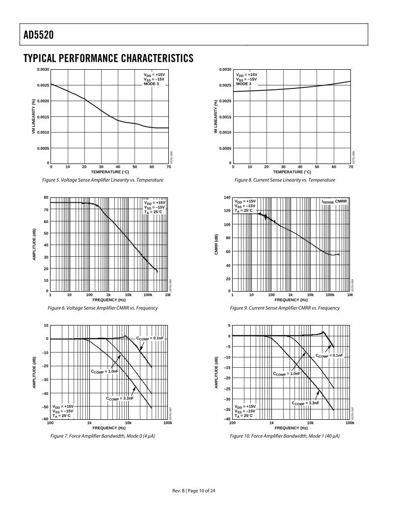
Figure 5. Voltage Sense Amplifier Linearity vs. Temperature
VDD = +15VVSS = –15VTA = 25°C
FREQUENCY (Hz)
AM
PLIT
UD
E (d
B)
80
10
20
30
50
60
40
70
01 10 100 1k 10k 100k 1M
0370
1-00
6
Figure 6. Voltage Sense Amplifier CMRR vs. Frequency
VDD = +15VVSS = –15VTA = 25°C
CCOMP = 0.1nF
CCOMP = 3.3nF
CCOMP = 1.0nF
FREQUENCY (Hz)
AM
PLIT
UD
E (d
B)
10
–50
–30
–20
–10
0
–40
–60100 1k 10k 100k
0370
1-00
7
Figure 7. Force Amplifier Bandwidth, Mode 0 (4 μA)
VDD = +15VVSS = –15VMODE 3
TEMPERATURE (°C)
IM L
INEA
RIT
Y (%
)
0.0030
0.0005
0.0010
0.0015
0.0020
0.0025
00 10 20 30 40 50 60 70
0370
1-00
8
Figure 8. Current Sense Linearity vs. Temperature
VDD = +15VVSS = –15VTA = 25°C
ISENSE CMRR
FREQUENCY (Hz)
CM
RR
(dB
)
140
20
60
80
100
120
40
01 10 100 1k 10k 100k 1M
0370
1-00
9
Figure 9. Current Sense Amplifier CMRR vs. Frequency
VDD = +15VVSS = –15VTA = 25°C
CCOMP = 0.1nF
CCOMP = 3.3nF
CCOMP = 1.0nF
FREQUENCY (Hz)
AM
PLIT
UD
E (d
B)
5
–35
–25
–20
–15
–10
–5
0
–30
–40100 1k 10k 100k
0370
1-01
0
Figure 10. Force Amplifier Bandwidth, Mode 1 (40 μA)
AD5520
Rev. B | Page 11 of 24
VDD = +15VVSS = –15VTA = 25°C
CCOMP = 0.1nF
CCOMP = 3.3nF
CCOMP = 1.0nF
FREQUENCY (Hz)
AM
PLIT
UD
E (d
B)
–35
–25
–20
–15
–10
–5
0
–30
–45
–40
100 1k 10k 100k
0370
1-01
1
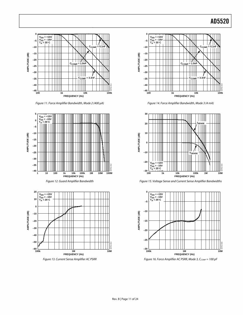
Figure 11. Force Amplifier Bandwidth, Mode 2 (400 μA)
VDD = +15VVSS = –15VTA = 25°C
FREQUENCY (Hz)
AM
PLIT
UD
E (d
B)
5
–35
–25
–20
–15
–10
–5
0
–30
–401 1k10010 1M100k10k 10M 100M
0370
1-01
2
Figure 12. Guard Amplifier Bandwidth
VDD = +15VVSS = –15VTA = 25°C
FREQUENCY (Hz)
AM
PLIT
UD
E (d
B)
20
–50
–40
–30
–20
–10
0
10
–60100k 1M 10M
0370
1-01
3
Figure 13. Current Sense Amplifier AC PSRR
VDD = +15VVSS = –15VTA = 25°C
CCOMP = 0.1nF
CCOMP = 3.3nF
CCOMP = 1.0nF
FREQUENCY (Hz)
AM
PLIT
UD
E (d
B)
–35
–25
–20
–15
–10
–5
0
–30
–45
–40
100 1k 10k 100k
0370
1-01
4
Figure 14. Force Amplifier Bandwidth, Mode 3 (4 mA)
VDD = +15VVSS = –15VTA = 25°C
FREQUENCY (Hz)
AM
PLIT
UD
E (d
B)
30
–20
0
–10
10
20
–30100 1k 1M100k10k 10M
0370
1-01
5
VSENSE
ISENSE
Figure 15. Voltage Sense and Current Sense Amplifier Bandwidths
FREQUENCY (Hz)
AM
PLIT
UD
E (d
B)
0
–25
–20
–10
–30
–15
–5
100k 1M 10M
0370
1-01
6
VDD = +15VVSS = –15VTA = 25°C
Figure 16. Force Amplifier AC PSRR, Mode 3, CCOMP = 100 pF
AD5520
Rev. B | Page 12 of 24
FREQUENCY (Hz)
AM
PLIT
UD
E (d
B)
20
10
0
–50
–40
–20
–60
–30
–10
100k 1M 10M
0370
1-01
7
VDD = +15VVSS = –15VTA = 25°C
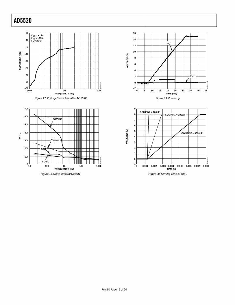
Figure 17. Voltage Sense Amplifier AC PSRR
FREQUENCY (Hz)
nV/√
Hz
700
100
300
200
400
500
600
010 100 10k1k 100k
0370
1-01
8
ISENSE
VSENSE
FOH
GUARD
Figure 18. Noise Spectral Density
TIME (ms)
VOLT
AG
E (V
)
16
0
6
8
4
2
10
12
14
–20 5 3525 3010 15 20 4540
0370
1-01
9
VCC
VDUT
Figure 19. Power Up
TIME (s)
VOLT
AG
E (V
)
9
0
3
4
2
1
5
6
7
8
–10 0.0060.004 0.0050.001 0.002 0.003 0.0080.007
0370
1-02
0
COMPIN2 = 100pFCOMPIN1 = 1000pF
COMPIN2 = 3000pF
Figure 20. Settling Time, Mode 2
AD5520
Rev. B | Page 13 of 24
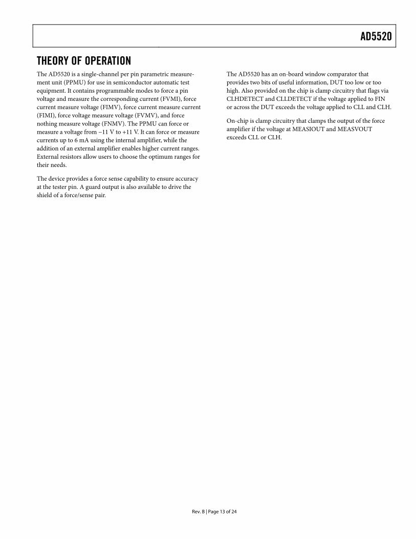
THEORY OF OPERATION The AD5520 is a single-channel per pin parametric measure-ment unit (PPMU) for use in semiconductor automatic test equipment. It contains programmable modes to force a pin voltage and measure the corresponding current (FVMI), force current measure voltage (FIMV), force current measure current (FIMI), force voltage measure voltage (FVMV), and force nothing measure voltage (FNMV). The PPMU can force or measure a voltage from −11 V to +11 V. It can force or measure currents up to 6 mA using the internal amplifier, while the addition of an external amplifier enables higher current ranges. External resistors allow users to choose the optimum ranges for their needs.
The device provides a force sense capability to ensure accuracy at the tester pin. A guard output is also available to drive the shield of a force/sense pair.
The AD5520 has an on-board window comparator that provides two bits of useful information, DUT too low or too high. Also provided on the chip is clamp circuitry that flags via CLHDETECT and CLLDETECT if the voltage applied to FIN or across the DUT exceeds the voltage applied to CLL and CLH.
On-chip is clamp circuitry that clamps the output of the force amplifier if the voltage at MEASIOUT and MEASVOUT exceeds CLL or CLH.
AD5520
Rev. B | Page 14 of 24
INTERFACE The AD5520 PPMU is controlled via a number of digital inputs, which are discussed in detail in the following sections. All inputs are TTL-compatible. CS is used to select the device while STB (active low input) latches data available on the other digital inputs and updates any required digital outputs. The rising edge of STB triggers sequence inputs. The remaining digital inputs control the function of the PMU. They also determine which measure mode the PMU is in, the compensation capacitor used, and the selected current range.
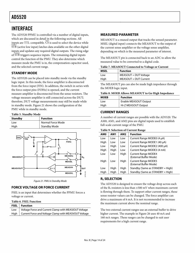
STANDBY MODE The AD5520 can be placed into standby mode via the standby logic input. In this mode, the force amplifier is disconnected from the force input (FIN). In addition, the switch in series with the force output pins (FOHx) is opened, and the current measure amplifier is disconnected from the sense resistors. The voltage measure amplifier is still connected across the DUT; therefore, DUT voltage measurements may still be made while in standby mode. Figure 21 shows the configuration of the PMU while in standby mode.
Table 5. Standby Mode Standby Function Low Normal Force Mode High Standby Mode
DAC
MEASIHx
MEASIL
MEASVH
MEASVL
FOHx
RS
DUT
FIN
MEASIOUT
MEASVOUT
G = 16
G = 1
0370
1-02
1
Figure 21. PMU in Standby Mode
FORCE VOLTAGE OR FORCE CURRENT FSEL is an input that determines whether the PPMU forces a voltage or current.
Table 6. FSEL Function FSEL Function Low Voltage Force and Current Clamp with MEASIOUT Voltage High Current Force and Voltage Clamp with MEASVOUT Voltage
MEASURED PARAMETER MEASOUT is a muxed output that tracks the sensed parameter. MSEL (digital input) connects the MEASOUT to the output of the current sense amplifier or the voltage sense amplifier, depending on which is the measured parameter of interest.
The MEASOUT pin is connected back to an ADC to allow the measured value to be converted to a digital code.
Table 7. MEASOUT Connected to Voltage or Current MSEL Function Low MEASOUT = DUT Voltage High MEASOUT = DUT Current
The MEASOUT pin can also be made high impedance through the MOEB logic input.
Table 8. MOEB Allows MEASOUT to Go High Impedance MOEB Function Low Enable MEASOUT Output High Hi-Z MEASOUT Output
CURRENT RANGES A number of current ranges are possible with the AD5520. The AM0, AM1, and AM2 pins are digital inputs used to establish full-scale current range of the PMU.
Table 9. Selection of Current Range AM0 AM1 AM2 Function Low Low Low Current Range MODE0 (4 μA) High Low Low Current Range MODE1 (40 μA) Low High Low Current Range MODE2 (400 μA) High High Low Current Range MODE3 (4 mA) Low Low High Current Range MODE4
(External Buffer Mode) High Low High Current Range MODE5
(External Buffer Mode) Low High High Standby (Same as STANDBY = High) High High High Standby (Same as STANDBY = High)
RS SELECTION The AD5520 is designed to ensure the voltage drop across each of the RS resistors is less than ±500 mV when maximum current is flowing through them. To support other current ranges, these sense resistor values can be changed. The force amplifier can drive a maximum of 6 mA. It is not recommended to increase the maximum current above the nominal range.
The two external current ranges use an external buffer to drive higher current. The example in Figure 26 uses 40 mA and 160 mA ranges. These ranges can be changed to suit user requirements for a high current range.
AD5520
Rev. B | Page 15 of 24
FORCE CONTROL AMPLIFIER The force control amplifier requires external capacitors connected between the COMPOUTx and COMPINx pins. For stability with large capacitance at the DUT, the largest capacitance value (3000 pF) should be selected. The force control amplifier should always contribute the dominant pole in the control loop. Settling times increase with larger capacitances. ACx inputs select which external compensation capacitor is used.
Table 10. AC0, AC1 Compensation Capacitor Selection AC0 AC1 Function Low Low Select External Compensation Capacitor 0 High Low Select External Compensation Capacitor 1 Low High Select External Compensation Capacitor 2
COMPARATOR FUNCTION AND STROBING The AD5520 has an on-board window comparator that provides two bits of useful information, DUT too low or DUT too high. CPSEL is the digital input that controls this function, selecting whether it should compare to the voltage sense or the current sense amplifier.
Table 11. Comparator Function Select CPSEL Function Low Compare CPL, CPH to MEASVOUT High Compare CPL, CPH to MEASIOUT
After CPSEL has selected which amplifier output is of interest, logic input CPCK is used to initiate comparator sampling and update the logic outputs CPOH and CPOL. This indicates whether the voltages at MEASIOUT or MEASVOUT have exceeded voltages set at CPL or CPH (thus providing DUT too high or DUT too low information). A rising edge on STB is required to clock the CPOH and CPOL data out.
Table 12. CPCK Synchronous Logic Outputs CPOH Function Low High
MEASVOUT or MEASIOUT < CPH MEASVOUT or MEASIOUT > CPH
CPOL Function Low High
MEASVOUT or MEASIOUT > CPL MEASVOUT or MEASIOUT < CPL
CLAMP FUNCTION Clamp circuitry, which is also included on-chip, clamps the force amplifier’s output if the voltage or current applied to the DUT exceeds the clamp levels, CLL and CLH. The clamp circuitry also comes into play in the event of a short or open circuit. When in force current range, the voltage clamps protect the DUT from an open circuit. Likewise, when forcing a voltage and a short circuit occurs, the current clamps protect the DUT. The clamps also function to protect the DUT if a transient voltage or current spike occurs when changing to a different operating mode, or when programming the device to a different current range.
The digital output flags, which indicate a clamp limit has been hit, are CLHDETECT for the upper clamp, and CLLDETECT output for the lower clamp.
Table 13. Clamp Detect Outputs CLHDETECT Function Low Upper Clamp Inactive High Upper Clamp Active
CLLDETECT Function Low Lower Clamp Inactive High Lower Clamp Active
HIGH CURRENT RANGES With the use of an external high current amplifier, two high current ranges are possible. The current range values can be set as required in the application through appropriate selection of the sense resistors connected between MEASI5H, MEASI4H, and MEASIL. When one of these high current ranges (Mode 4 or Mode 5) is selected via the AMx control lines, the appro-priate QM4 or QM5 output is enabled. As a result, these outputs can be used to control relays connected in series with the high current amplifier, as shown in Figure 26.
Table 14. High Current Range Logic Outputs QM4 QM5 Function High Low Current Range Mode 4 Enable Output Low High Current Range Mode 5 Enable Output
AD5520
Rev. B | Page 16 of 24
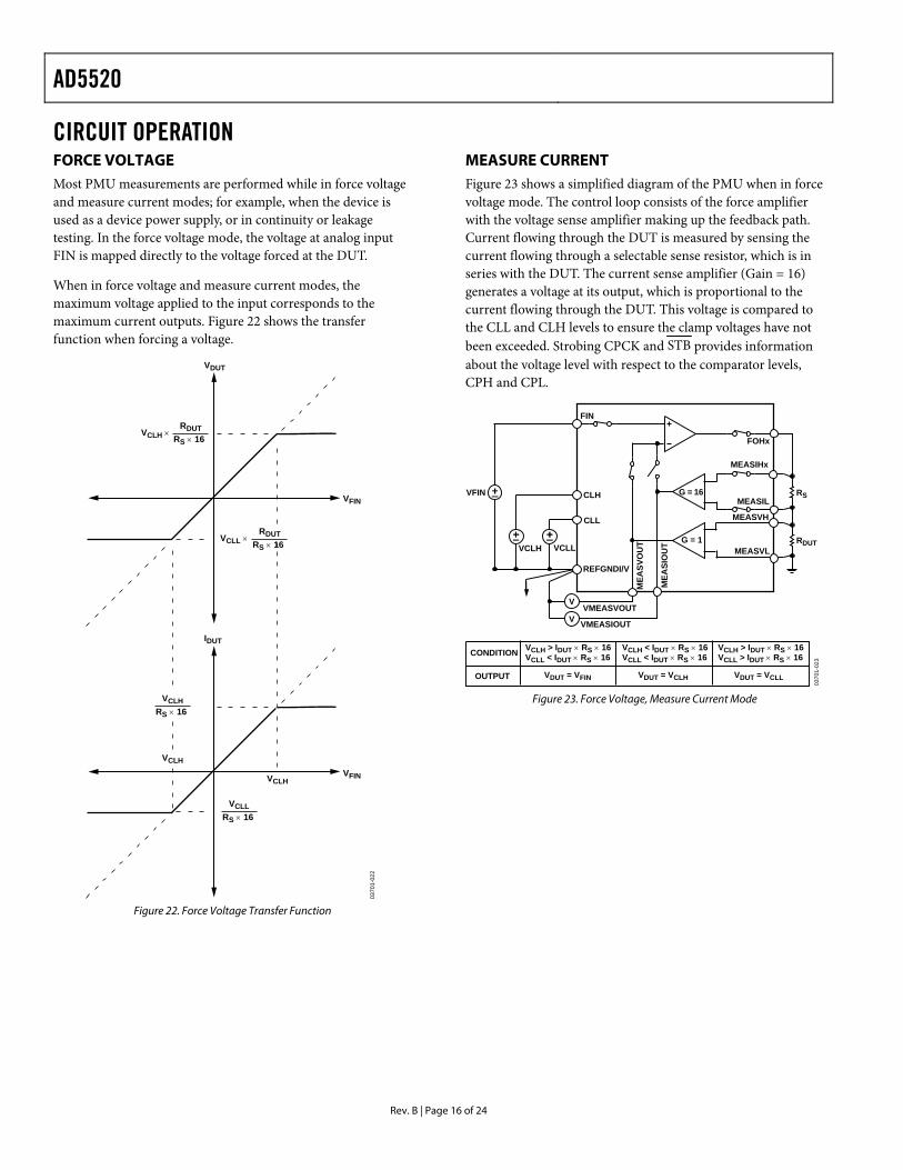
CIRCUIT OPERATION FORCE VOLTAGE Most PMU measurements are performed while in force voltage and measure current modes; for example, when the device is used as a device power supply, or in continuity or leakage testing. In the force voltage mode, the voltage at analog input FIN is mapped directly to the voltage forced at the DUT.
When in force voltage and measure current modes, the maximum voltage applied to the input corresponds to the maximum current outputs. Figure 22 shows the transfer function when forcing a voltage.
VDUT
VCLL ×RS × 16
RDUT
VCLH ×RS × 16
RDUT
RS × 16VCLH
RS × 16VCLL
VCLH
VCLH
IDUT
VFIN
VFIN
0370
1-02
2
Figure 22. Force Voltage Transfer Function
MEASURE CURRENT Figure 23 shows a simplified diagram of the PMU when in force voltage mode. The control loop consists of the force amplifier with the voltage sense amplifier making up the feedback path. Current flowing through the DUT is measured by sensing the current flowing through a selectable sense resistor, which is in series with the DUT. The current sense amplifier (Gain = 16) generates a voltage at its output, which is proportional to the current flowing through the DUT. This voltage is compared to the CLL and CLH levels to ensure the clamp voltages have not been exceeded. Strobing CPCK and STB provides information about the voltage level with respect to the comparator levels, CPH and CPL.
MEASIHx
MEASILG = 16
MEASVH
MEASVLG = 1
FOHx
RS
RDUT
FIN
VMEASIOUT
VMEASVOUT
MEA
SIO
UT
MEA
SVO
UT
CLH
CLL
VCLLVCLH
VFIN
CONDITION
OUTPUT
VCLH > IDUT × RS × 16VCLL < IDUT × RS × 16
VDUT = VFIN VDUT = VCLH VDUT = VCLL
VCLH > IDUT × RS × 16VCLL > IDUT × RS × 16
VCLH < IDUT × RS × 16VCLL < IDUT × RS × 16
REFGNDI/V
V
V
0370
1-02
3
Figure 23. Force Voltage, Measure Current Mode
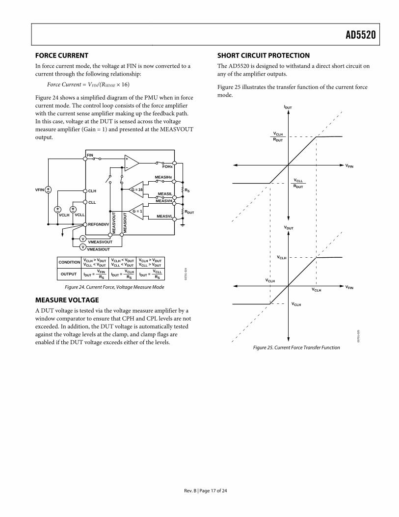
AD5520
Rev. B | Page 17 of 24
FORCE CURRENT In force current mode, the voltage at FIN is now converted to a current through the following relationship:
Force Current = VFIN/(RSENSE × 16)
Figure 24 shows a simplified diagram of the PMU when in force current mode. The control loop consists of the force amplifier with the current sense amplifier making up the feedback path. In this case, voltage at the DUT is sensed across the voltage measure amplifier (Gain = 1) and presented at the MEASVOUT output.
MEASIHx
MEASILG = 16
MEASVH
MEASVLG = 1
FOHx
RS
RDUT
FIN
VMEASIOUT
VMEASVOUT
MEA
SIO
UT
MEA
SVO
UT
CLH
CLL
VCLLVCLH
VFIN
CONDITION
OUTPUT
VCLH > VDUTVCLL < VDUT
VCLH > VDUTVCLL > VDUT
VCLH < VDUTVCLL < VDUT
REFGNDI/V
V
V
0370
1-02
4
IDUT = RS
VFIN IDUT = RS
VCLH IDUT = RS
VCLL
Figure 24. Current Force, Voltage Measure Mode
MEASURE VOLTAGE A DUT voltage is tested via the voltage measure amplifier by a window comparator to ensure that CPH and CPL levels are not exceeded. In addition, the DUT voltage is automatically tested against the voltage levels at the clamp, and clamp flags are enabled if the DUT voltage exceeds either of the levels.
SHORT CIRCUIT PROTECTION The AD5520 is designed to withstand a direct short circuit on any of the amplifier outputs.
Figure 25 illustrates the transfer function of the current force mode.
IDUT
RDUT
VCLL
RDUT
VCLH
VCLH
VCLH
VCLH
VCLH
VDUT
VFIN
VFIN
0370
1-02
5
Figure 25. Current Force Transfer Function

AD5520
Rev. B | Page 18 of 24
SETTLING TIME CONSIDERATIONS Fast throughput is a key requirement in automatic test equipment because it relates directly to the cost of manufac-turing the DUT; thus reducing the time required to make a measurement is of greatest importance. When taking measurements using a PMU, the limiting factor is usually the time it takes the output to settle to the required accuracy so a measurement can be taken. DUT capacitance, measurement accuracy, and the design of the PMU are the major contributors to this time.
Figure 26 shows a simplified block diagram of the AD5520 PMU. In brief, the device consists of a force control amplifier, access to a number of selectable sense resistors, a voltage measure instrumentation amplifier, and a current measure instrumentation amplifier. To optimize the performance of the device, there are also nodes provided where external compensa-tion capacitors are added. As mentioned, making an accurate measurement in the fastest time while avoiding overshoots and ringing is the key requirement in any automatic test equipment (ATE) system. Doing so provides challenges, however. The external compensation capacitors set up different settling times or bandwidths on the force control amplifier, and while one compensation capacitor value may suit one range, it may not suit other ranges. To optimize measurement performance and speed, differences in signal behavior on each range and frequency of use of each range need to be taken into account.
When selecting a faster settling time, there is a trade-off. A small compensation value results in faster settling, but may incur penalties in overshoots or ringing at the DUT. Compensation capacitor selection should be optimized to ensure minimum overshoots while still giving decent settling time performance.
While careful selection of the compensation capacitor is required to minimize the settling time, another factor can greatly contribute to the overall settling of the loop if the feedback loop is broken in some manner, and the force control amplifier goes to either the positive or negative rails. There is a finite amount of time required for the amplifier to recover from this condition, typically 85 μs, which adds to the settling of the loop. Ensuring that the force control amplifier never goes into saturation is the best solution. This solution can be helped by putting the device into standby mode any time the operating mode or range selection is changed. In addition, ensure that the selected output range can supply the required current needed by the DUT.
AD5520
Rev. B | Page 19 of 24
PCB LAYOUT AND POWER SUPPLY DECOUPLING In any circuit where accuracy is important, careful considera-tion to the power supply and the ground return layout helps to ensure the rated performance. The printed circuit board on which the AD5520 is mounted should be designed so that the analog and digital sections are separated and confined to certain areas of the board. If the PMU is in a system where multiple devices require an AGND-to-DGND connection, the connection should be made at one point only. The star ground point should be established as close as possible to the device.
This PMU should have ample supply bypassing of 10 μF in parallel with 0.1 μF on the supply and should be located as close as possible to the package, ideally right up against the device. The 0.1 μF capacitor should have low effective series resistance (ESR) and effective series inductance (ESI), such as the common ceramic types that provide a low impedance path to ground at high frequencies, to handle transient currents due to internal logic switching. Low ESR (1 μF to 10 μF) tantalum or electrolytic capacitors should also be applied at the supplies to minimize transient disturbance and filter out low frequency ripple.
Fast switching signals, such as clocks, should be shielded with digital ground to avoid radiating noise to other parts of the board and should never be run near the reference inputs.
Avoid crossover of digital and analog signals. Traces on opposite sides of the board should run at right angles to each other. This reduces the effects of feedthrough through the board. A microstrip technique is by far the best but not always possible with a double-sided board. In this technique, the component side of the board is dedicated to the ground plane while signal traces are placed on the solder side.
It is good practice to use compact, minimum lead length PCB layout design. Leads to the input should be as short as possible to minimize IR drops and stray inductance.
AD5520
Rev. B | Page 20 of 24
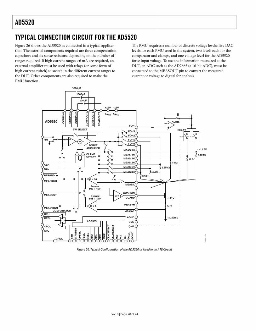
TYPICAL CONNECTION CIRCUIT FOR THE AD5520 Figure 26 shows the AD5520 as connected in a typical applica-tion. The external components required are three compensation capacitors and six sense resistors, depending on the number of ranges required. If high current ranges >6 mA are required, an external amplifier must be used with relays (or some form of high current switch) to switch in the different current ranges to the DUT. Other components are also required to make the PMU function.
The PMU requires a number of discrete voltage levels: five DAC levels for each PMU used in the system, two levels each for the comparator and clamps, and one voltage level for the AD5520 force input voltage. To use the information measured at the DUT, an ADC such as the AD7665 (a 16-bit ADC), must be connected to the MEASOUT pin to convert the measured current or voltage to digital for analysis.
CLL
DET
ECT
MEASI4H
FIN
BW SELECT
CO
MPO
UT2
FOH1FOH2FOH3
FOH0
AVEE AVCC
MEASI3H
CLHCLL
REFGND
MEASIOUT
MEASOUT
MEASVOUT
CPHCPOH
CPOLCPL
MEASI5H
MEASIL
GUARDIN
GUARD
MEASVH
MEASVL
AGND
QM5
QM4
DG
ND
DV D
D
CS
STA
ND
BY
CO
MPO
UT1
CO
MPO
UT0
CO
MPI
N2
CO
MPI
N1
CO
MPI
N0
CLAMPDETECT
ISENSEINST AMP
VSENSEINST AMP
LOGICS
AC
0A
C1
CLH
DET
ECT
MO
E
AM
0A
M1
AM
2M
SEL
FSEL
CPS
EL
STB
CPCK
AD5520
COMPARATOR
125kΩ12.5kΩ
1.25kΩ125Ω
12.5Ω3.126Ω
AD815
RELAY
<±11.5V
DUT
<±100mV
±11V≥
MEASI2HMEASI1H
MEASI0H
+15V –15V
100pF
1000pF
3000pF
FOH
FORCEAMPLIFIER
G = 16
G = 1
G = 1
0370
1-02
6
Figure 26. Typical Configuration of the AD5520 as Used in an ATE Circuit
AD5520
Rev. B | Page 21 of 24
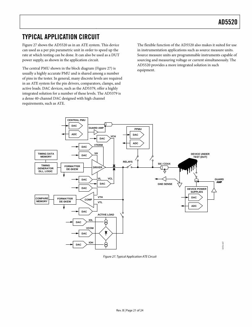
TYPICAL APPLICATION CIRCUIT Figure 27 shows the AD5520 as in an ATE system. This device can used as a per pin parametric unit in order to speed up the rate at which testing can be done. It can also be used as a DUT power supply, as shown in the application circuit.
The central PMU shown in the block diagram (Figure 27) is usually a highly accurate PMU and is shared among a number of pins in the tester. In general, many discrete levels are required in an ATE system for the pin drivers, comparators, clamps, and active loads. DAC devices, such as the AD5379, offer a highly integrated solution for a number of these levels. The AD5379 is a dense 40-channel DAC designed with high channel requirements, such as ATE.
The flexible function of the AD5520 also makes it suited for use in instrumentation applications such as source measure units. Source measure units are programmable instruments capable of sourcing and measuring voltage or current simultaneously. The AD5520 provides a more integrated solution in such equipment.
CENTRAL PMU
ADC
DAC
TIMING DATAMEMORY
TIMINGGENERATORDLL, LOGIC
FORMATTERDE-SKEW
DAC
DAC
DACVTERM
DRIVER
DAC
DACDAC
IOL
VH
COMPCOMPAREMEMORY
DACACTIVE LOAD
DAC
DAC
VCOM
IOHDAC
VTH
VTL
VCL
PPMU
ADC
DAC
DEVICE POWERSUPPLIES
ADC
DAC
GND SENSE
GUARDAMPAMP
50Ω COAXRELAYS
DEVICE UNDERTEST (DUT)
GUARD AMP
VL
VCH
FORMATTERDE-SKEW
0370
1-02
7
Figure 27. Typical Application ATE Circuit
AD5520
Rev. B | Page 22 of 24
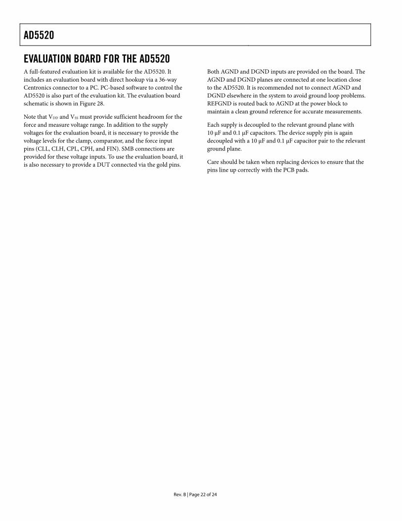
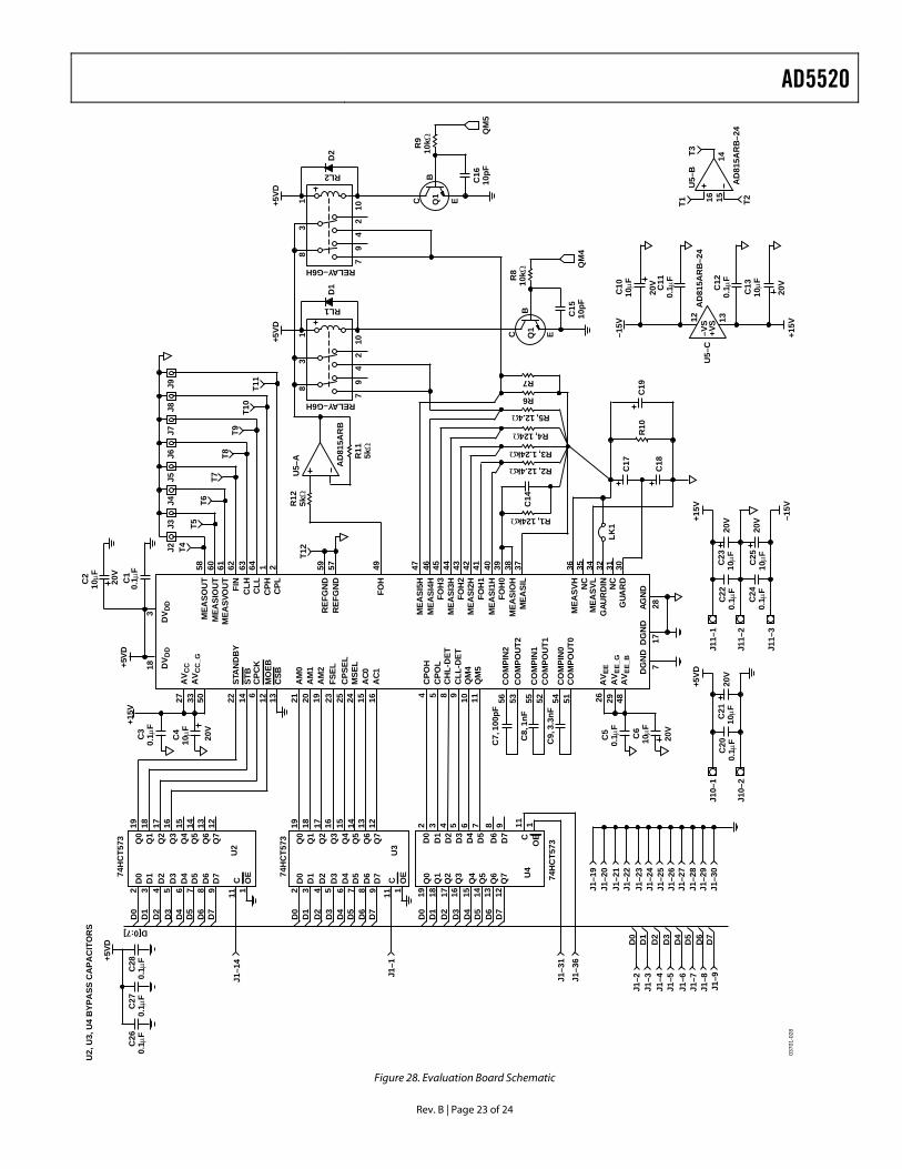
EVALUATION BOARD FOR THE AD5520 A full-featured evaluation kit is available for the AD5520. It includes an evaluation board with direct hookup via a 36-way Centronics connector to a PC. PC-based software to control the AD5520 is also part of the evaluation kit. The evaluation board schematic is shown in Figure 28.
Note that VDD and VSS must provide sufficient headroom for the force and measure voltage range. In addition to the supply voltages for the evaluation board, it is necessary to provide the voltage levels for the clamp, comparator, and the force input pins (CLL, CLH, CPL, CPH, and FIN). SMB connections are provided for these voltage inputs. To use the evaluation board, it is also necessary to provide a DUT connected via the gold pins.
Both AGND and DGND inputs are provided on the board. The AGND and DGND planes are connected at one location close to the AD5520. It is recommended not to connect AGND and DGND elsewhere in the system to avoid ground loop problems. REFGND is routed back to AGND at the power block to maintain a clean ground reference for accurate measurements.
Each supply is decoupled to the relevant ground plane with 10 μF and 0.1 μF capacitors. The device supply pin is again decoupled with a 10 μF and 0.1 μF capacitor pair to the relevant ground plane.
Care should be taken when replacing devices to ensure that the pins line up correctly with the PCB pads.
AD5520
Rev. B | Page 23 of 24
AV C
C27
AV C
C_G
33 50
STA
ND
BY
22
STB
14C
PCK
6
MO
EB12
CSB
13
AM
021
AM
120
AM
219
FSEL
23
CPS
EL25
MSE
L24
AC0
15
AC1
16
CPO
H4
CPO
L5
CH
L-D
ET8
CLL
-DET
9Q
M4
10Q
M5
11
CO
MPI
N2
56
CO
MPO
UT2
53
CO
MPI
N1
55
CO
MPO
UT1
52
CO
MPI
N0
54
CO
MPO
UT0
51
DG
ND
26
AV E
E_G
29A
V EE_
B48
58 60 61 62 63 64 1 2 59 57 49 47 46 45 44 43 42 41 40 39 38 37 32 31 30
MEA
SOU
TM
EASI
OU
TM
EASV
OU
TFI
NC
LH CLL
CPH CPL
REF
GN
DR
EFG
ND
FOH
MEA
SI5H
MEA
SI4H
FOH
3M
EASI
3HFO
H2
MEA
SI2H
FOH
1M
EASI
1HFO
H0
MEA
SIO
HM
EASI
L
GAU
RD
IN NC
GUA
RD
36 35 34
MEA
SVH
NC
MEA
SVL
+15V
C3
0.1μ
F
C4
10μF 20V
Q0
1516171819 14 13 12
Q1
Q2
Q3
Q4
Q5
Q6
Q7
D0
D1
D2
D3
D4
D5
D6
D7
65432 7 8 9
C OE
11 1
D0
D1
D2
D3
D4
D5
D6
D7
Q0
1516171819 14 13 12
Q1
Q2
Q3
Q4
Q5
Q6
Q7
D0
D1
D2
D3
D4
D5
D6
D7
65432 7 8 9
C OE
11 1
D0
D1
D2
D3
D4
D5
D6
D7
Q0
1516171819 14 13 12
Q1
Q2
Q3
Q4
Q5
Q6
Q7
D0
D1
D2
D3
D4
D5
D6
D7
65432 7 8 9
CO
E
11 1
D0
D1
D2
D3
D4
D5
D6
D7
C7,
100
pF
C8,
1nF
C9,
3.3
nF
C5
0.1μ
F
20V
C6
10μF
D[0:7]
C26
0.1μ
FC
270.
1μF
C28
0.1μ
F
U2,
U3,
U4
BYP
ASS
CA
PAC
ITO
RS
+5VD
J1–1
4
J1–1
J1–3
1J1
–36
J1–6
J1–5
J1–4
J1–3
J1–2
J1–7
J1–8
J1–9
D0
D1
D2
D3
D4
D5
D6
D7
J1–2
3J1
–22
J1–2
1J1
–20
J1–1
9
J1–2
4J1
–25
J1–2
6J1
–27
J1–2
8J1
–29
J1–3
0C
200.
1μF
C21
10μF
+5VD
J10–
1
J10–
2
20V
C22
0.1μ
FC
2310
μF
J11–
1
J11–
2
20V
C24
0.1μ
FC
2510
μFJ1
1–3
20V
717
28D
GN
DAG
ND
DV D
DD
V DD
C1
0.1μ
F
C2
10μF 20V
183
T4J2
T5J3
T6J4
T7J5
T8J6
T9J7
T10
J8
T11
J9
T12
U5–
A
AD
815A
RB
R12
5kΩ
R11
5kΩ
RELAY–G6H
RL1
83
1
97
42
10
D1
RELAY–G6H
RL2
83
1
97
42
10
D2
R2, 12.4kΩ
R1, 124kΩ
C14
R3, 1.24kΩ
R4, 124Ω
R5, 12.4Ω
R6
R7
LK1
C17
C18
R10
C19
C15
10pF
Q1 EC
BR
810
kΩ
QM
4
C16
10pF
Q1 EC
BR
910
kΩ
QM
5
–VS
+VS
C10
10μF
20V
C13
10μF
20V
–15V
C11
0.1μ
F
C12
0.1μ
F
U5–
CA
D81
5AR
B–2
412 13
+15V
T1 T2
T3 14
AD
815A
RB
–24
1516
U5–
B
74H
CT5
73
74H
CT5
73
74H
CT5
73
U2
U3
U4
AV E
E
+15V
–15V
+5VD
+5VD
+5VD
0370
1-02
8
Figure 28. Evaluation Board Schematic
AD5520 Preliminary Technical Data
Rev. B | Page 24 of 24
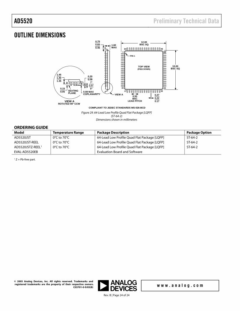
OUTLINE DIMENSIONS
COMPLIANT TO JEDEC STANDARDS MS-026-BCD
TOP VIEW(PINS DOWN)
1
1617
3332
484964
0.270.220.17
0.50BSC
LEAD PITCH
10.00BSC SQ
12.00BSC SQ
PIN 1
1.60MAX
0.750.600.45
VIEW A
0.20 0.09
1.451.401.35
0.08 MAXCOPLANARITY
VIEW AROTATED 90° CCW
SEATINGPLANE
0.150.05
7°3.5°0°
Figure 29. 64-Lead Low Profile Quad Flat Package [LQFP]
(ST-64-2) Dimensions shown in millimeters
ORDERING GUIDE Model Temperature Range Package Description Package Option AD5520JST 0°C to 70°C 64-Lead Low Profile Quad Flat Package [LQFP] ST-64-2 AD5520JST-REEL 0°C to 70°C 64-Lead Low Profile Quad Flat Package [LQFP] ST-64-2 AD5520JSTZ-REEL1 0°C to 70°C 64-Lead Low Profile Quad Flat Package [LQFP] ST-64-2 EVAL-AD5520EB Evaluation Board and Software 1 Z = Pb-free part.
© 2005 Analog Devices, Inc. All rights reserved. Trademarks and registered trademarks are the property of their respective owners. C03701-0-9/05(B)