ac voltage controller circuits (rms voltage...
TRANSCRIPT

1
AC VOLTAGE CONTROLLER CIRCUITS
(RMS VOLTAGE CONTROLLERS)
AC voltage controllers (ac line voltage controllers) are employed to vary the RMS value of the alternating voltage applied to a load circuit by introducing Thyristors between the load and a constant voltage ac source. The RMS value of alternating voltage applied to a load circuit is controlled by controlling the triggering angle of the Thyristors in the ac voltage controller circuits.
In brief, an ac voltage controller is a type of thyristor power converter which is used to convert a fixed voltage, fixed frequency ac input supply to obtain a variable voltage ac output. The RMS value of the ac output voltage and the ac power flow to the load is controlled by varying (adjusting) the trigger angle ‘α’
ACVoltage
Controller
V0(RMS)
fS
Variable AC RMS O/P Voltage
ACInput
Voltagefs
Vs
fs
There are two different types of thyristor control used in practice to control the ac power flow
• On-Off control• Phase control
These are the two ac output voltage control techniques. In On-Off control technique Thyristors are used as switches to connect the load circuit
to the ac supply (source) for a few cycles of the input ac supply and then to disconnect it for few input cycles. The Thyristors thus act as a high speed contactor (or high speed ac switch).
PHASE CONTROL In phase control the Thyristors are used as switches to connect the load circuit to
the input ac supply, for a part of every input cycle. That is the ac supply voltage is chopped using Thyristors during a part of each input cycle.
The thyristor switch is turned on for a part of every half cycle, so that input supply voltage appears across the load and then turned off during the remaining part of input half cycle to disconnect the ac supply from the load.
By controlling the phase angle or the trigger angle ‘α’ (delay angle), the output RMS voltage across the load can be controlled.
The trigger delay angle ‘α’ is defined as the phase angle (the value of ωt) at which the thyristor turns on and the load current begins to flow.
Thyristor ac voltage controllers use ac line commutation or ac phase commutation. Thyristors in ac voltage controllers are line commutated (phase commutated) since the input supply is ac. When the input ac voltage reverses and becomes negative during the negative half cycle the current flowing through the conducting thyristor decreases and

2
falls to zero. Thus the ON thyristor naturally turns off, when the device current falls to zero.
Phase control Thyristors which are relatively inexpensive, converter grade Thyristors which are slower than fast switching inverter grade Thyristors are normally used.
For applications upto 400Hz, if Triacs are available to meet the voltage and current ratings of a particular application, Triacs are more commonly used.
Due to ac line commutation or natural commutation, there is no need of extra commutation circuitry or components and the circuits for ac voltage controllers are very simple.
Due to the nature of the output waveforms, the analysis, derivations of expressions for performance parameters are not simple, especially for the phase controlled ac voltage controllers with RL load. But however most of the practical loads are of the RL type and hence RL load should be considered in the analysis and design of ac voltage controller circuits.
TYPE OF AC VOLTAGE CONTROLLERS The ac voltage controllers are classified into two types based on the type of input
ac supply applied to the circuit. • Single Phase AC Controllers.• Three Phase AC Controllers.
Single phase ac controllers operate with single phase ac supply voltage of 230V RMS at 50Hz in our country. Three phase ac controllers operate with 3 phase ac supply of 400V RMS at 50Hz supply frequency.
Each type of controller may be sub divided into • Uni-directional or half wave ac controller.• Bi-directional or full wave ac controller.
In brief different types of ac voltage controllers are • Single phase half wave ac voltage controller (uni-directional controller).• Single phase full wave ac voltage controller (bi-directional controller).• Three phase half wave ac voltage controller (uni-directional controller).• Three phase full wave ac voltage controller (bi-directional controller).
APPLICATIONS OF AC VOLTAGE CONTROLLERS • Lighting / Illumination control in ac power circuits.• Induction heating.• Industrial heating & Domestic heating.• Transformer tap changing (on load transformer tap changing).• Speed control of induction motors (single phase and poly phase ac induction
motor control).• AC magnet controls.
PRINCIPLE OF ON-OFF CONTROL TECHNIQUE (INTEGRAL CYCLE CONTROL)
The basic principle of on-off control technique is explained with reference to a single phase full wave ac voltage controller circuit shown below. The thyristor switches
1T and 2T are turned on by applying appropriate gate trigger pulses to connect the input ac supply to the load for ‘n’ number of input cycles during the time interval ONt . The

3
thyristor switches 1T and 2T are turned off by blocking the gate trigger pulses for ‘m’ number of input cycles during the time interval OFFt . The ac controller ON time ONtusually consists of an integral number of input cycles.
LR R= = Load Resistance Fig.: Single phase full wave AC voltage controller circuit
Vs
Vo
io
ig1
ig2
wt
wt
wt
wt
Gate pulse of T1
Gate pulse of T2
n m
Fig.: Waveforms Example Referring to the waveforms of ON-OFF control technique in the above diagram,
n = Two input cycles. Thyristors are turned ON during ONt for two input cycles.

4
m = One input cycle. Thyristors are turned OFF during OFFt for one input cycle
Fig.: Power Factor
Thyristors are turned ON precisely at the zero voltage crossings of the input supply. The thyristor 1T is turned on at the beginning of each positive half cycle by applying the gate trigger pulses to 1T as shown, during the ON time ONt . The load current flows in the positive direction, which is the downward direction as shown in the circuit diagram when 1T conducts. The thyristor 2T is turned on at the beginning of each negative half cycle, by applying gating signal to the gate of 2T , during ONt . The load current flows in the reverse direction, which is the upward direction when 2T conducts. Thus we obtain a bi-directional load current flow (alternating load current flow) in a ac voltage controller circuit, by triggering the thyristors alternately.
This type of control is used in applications which have high mechanical inertia and high thermal time constant (Industrial heating and speed control of ac motors). Due to zero voltage and zero current switching of Thyristors, the harmonics generated by switching actions are reduced.
For a sine wave input supply voltage, sin 2 sins m Sv V t V tω ω= =
SV = RMS value of input ac supply = 2mV = RMS phase supply voltage.
If the input ac supply is connected to load for ‘n’ number of input cycles and disconnected for ‘m’ number of input cycles, then
,ON OFFt n T t m T= × = ×
Where 1Tf
= = input cycle time (time period) and
f = input supply frequency.
ONt = controller on time = n T× .
OFFt = controller off time = m T× .
OT = Output time period = ( ) ( )ON OFFt t nT mT+ = + .

5
We can show that,
Output RMS voltage ( ) ( )ON ON
SO RMS i RMSO O
t tV V VT T
= =
Where ( )i RMSV is the RMS input supply voltage = SV .
TO DERIVE AN EXPRESSION FOR THE RMS VALUE OF OUTPUT VOLTAGE, FOR ON-OFF CONTROL METHOD.
Output RMS voltage ( ) ( )2 2
0
1 .ONt
mO RMSO t
V V Sin t d tT
ω
ω
ω ωω =
= ∫
( ) ( )2
2
0
.ONt
mO RMS
O
VV Sin t d tT
ω
ω ωω
= ∫
Substituting for 2 1 22
CosSin θθ −=
( ) ( )2
0
1 22
ONtm
O RMSO
V Cos tV d tT
ω ω ωω
− = ∫
( ) ( ) ( )2
0 0
2 .2
ON ONt tm
O RMSO
VV d t Cos t d tT
ω ω
ω ω ωω
= −
∫ ∫
( ) ( )2
0 0
222
ON ONt tm
O RMSO
V Sin tV tT
ω ωωωω
= −
( ) ( )2 sin 2 sin 00
2 2m ON
ONO RMSO
V tV tT
ωωω
− = − −
Now ONt = An integral number of input cycles; Hence , 2 ,3 , 4 ,5 ,.....ONt T T T T T= & 2 ,4 ,6 ,8 ,10 ,......ONtω π π π π π=
Where T is the input supply time period (T = input cycle time period). Thus we note that sin 2 0ONtω =
( )
2
2 2m ON m ON
O RMSO O
V t V tVT T
ωω
= =
6
( ) ( )ON ON
SO RMS i RMSO O
t tV V VT T
= =
Where ( ) 2m
Si RMSVV V= = = RMS value of input supply voltage;
( )ON ON
O ON OFF
t t nT n kT t t nT mT n m
= = = =+ + +
= duty cycle (d).
( ) ( )S SO RMSnV V V k
m n= =
+
PERFORMANCE PARAMETERS OF AC VOLTAGE CONTROLLERS
• RMS Output (Load) Voltage
( ) ( ) ( )1
222 2
0
sin .2 mO RMS
nV V t d tn m
π
ω ωπ
= +
∫
( ) ( ) ( )2m
SO RMS i RMSV nV V k V k
m n= = =
+
( ) ( ) SO RMS i RMSV V k V k= =
Where ( )S i RMSV V= = RMS value of input supply voltage.
• Duty Cycle
( ) ( )ON ON
O ON OFF
t t nTkT t t m n T
= = =+ +
Where, ( )
nkm n
=+
= duty cycle (d).
• RMS Load Current
( )( ) ( )O RMS O RMS
O RMSL
V VI
Z R= = ; for a resistive load LZ R= .
• Output AC (Load) Power
( )2
O LO RMSP I R= ×

7
• Input Power Factor
output load powerinput supply volt amperes
O O
S S
P PPFVA V I
= = =
( )
( ) ( )
2LO RMS
i RMS in RMS
I RPF
V I×
=×
; ( )S in RMSI I= = RMS input supply current.
The input supply current is same as the load current in O LI I I= =
Hence, RMS supply current = RMS load current; ( ) ( )in RMS O RMSI I= .
( )
( ) ( )
( )
( )
( )
( )
2LO RMS O RMS i RMS
i RMS in RMS i RMS i RMS
I R V V kPF k
V I V V×
= = = =×
nPF km n
= =+
• The Average Current of Thyristor ( )T AvgI
0 π 2π 3π ωt
Im
n miT
Waveform of Thyristor Current
( ) ( ) ( )0
sin .2 mT Avg
nI I t d tm n
π
ω ωπ
=+ ∫
( ) ( ) ( )0
sin .2
mT Avg
nII t d tm n
π
ω ωπ
=+ ∫
( ) ( ) 0
cos2
mT Avg
nII tm n
π
ωπ
= − +
( ) ( ) [ ]cos cos 02
mT Avg
nIIm n
ππ
= − ++

8
( ) ( ) ( )1 12
mT Avg
nIIm nπ
= − − + +
( ) ( ) [ ]22 mT Avg
nI Im nπ
=+
( ) ( ).m m
T AvgI n k IIm nπ π
= =+
( ) ( )duty cycle ON
ON OFF
t nkt t n m
= = =+ +
( ) ( ).m m
T AvgI n k IIm nπ π
= =+
,
Where mm
L
VIR
= = maximum or peak thyristor current.
• RMS Current of Thyristor ( )T RMSI
( ) ( ) ( )1
22 2
0
sin .2 mT RMS
nI I t d tn m
π
ω ωπ
= +
∫
( ) ( ) ( )1
222
0
sin .2
mT RMS
nII t d tn m
π
ω ωπ
= +
∫
( ) ( )( ) ( )
122
0
1 cos 22 2
mT RMS
tnII d tn m
π ωω
π −
= + ∫
( ) ( ) ( ) ( )1
22
0 0
cos 2 .4
mT RMS
nII d t t d tn m
π π
ω ω ωπ
= − +
∫ ∫
( ) ( ) ( )1
22
0 0
sin 224
mT RMS
nI tI tn m
π πωωπ
= − +
( ) ( ) ( )1
22 sin 2 sin 004 2
mT RMS
nIIn m
πππ
− = − − +

9
( ) ( ) 1
22
0 04
mT RMS
nIIn m
ππ
= − − +
( ) ( ) ( )
1 12 22 2
4 4m m
T RMSnI nII
n m n mπ
π
= = + +
( ) ( )2 2m m
T RMSI InI k
m n= =
+
( ) 2m
T RMSII k=
PROBLEM 1. A single phase full wave ac voltage controller working on ON-OFF control
technique has supply voltage of 230V, RMS 50Hz, load = 50Ω. The controller isON for 30 cycles and off for 40 cycles. Calculate
• ON & OFF time intervals.• RMS output voltage.• Input P.F.• Average and RMS thyristor currents.
( ) 230in RMSV V= , 2 230 325.269mV V= × = V, 325.269mV V= ,
1 1 0.02sec50
Tf Hz
= = = , 20T ms= .
n = number of input cycles during which controller is ON; 30n = .
m = number of input cycles during which controller is OFF; 40m = .
30 20 600 0.6secONt n T ms ms= × = × = =
0.6secONt n T= × = = controller ON time.
40 20 800 0.8secOFFt m T ms ms= × = × = =0.8secOFFt m T= × = = controller OFF time.
Duty cycle ( ) ( )
30 0.428540 30
nkm n
= = =+ +
RMS output voltage
( ) ( ) ( )O RMS i RMSnV V
m n= ×
+

10
( ) ( )30 3230 230
30 40 7O RMSV V= × =+
( ) 230 0.42857 230 0.65465O RMSV V= = ×
( ) 150.570O RMSV V=
( )( ) ( ) 150.570 3.0114
50O RMS O RMS
O RMSL
V V VI AZ R
= = = =Ω
( )2 23.0114 50 453.426498O LO RMSP I R W= × = × =
Input Power Factor .P F k=
( )30 0.428570
nPFm n
= = =+
0.654653PF =
Average Thyristor Current Rating
( )m m
T AvgI k InI
m nπ π× = × = +
where 2 230 325.26950 50
mm
L
VIR
×= = =
6.505382mI A= = Peak (maximum) thyristor current.
( )6.505382 3
7T AvgIπ
= ×
( ) 0.88745T AvgI A=
RMS Current Rating of Thyristor
( ) ( )6.505382 3
2 2 2 7m m
T RMSI InI k
m n= = = ×
+
( ) 2.129386T RMSI A=

11
PRINCIPLE OF AC PHASE CONTROL The basic principle of ac phase control technique is explained with reference to a
single phase half wave ac voltage controller (unidirectional controller) circuit shown in the below figure.
The half wave ac controller uses one thyristor and one diode connected in parallel across each other in opposite direction that is anode of thyristor 1T is connected to the cathode of diode 1D and the cathode of 1T is connected to the anode of 1D . The output voltage across the load resistor ‘R’ and hence the ac power flow to the load is controlled by varying the trigger angle ‘α’.
The trigger angle or the delay angle ‘α’ refers to the value of tω or the instant at which the thyristor 1T is triggered to turn it ON, by applying a suitable gate trigger pulse between the gate and cathode lead.
The thyristor 1T is forward biased during the positive half cycle of input ac supply. It can be triggered and made to conduct by applying a suitable gate trigger pulse only during the positive half cycle of input supply. When 1T is triggered it conducts and the load current flows through the thyristor 1T , the load and through the transformer secondary winding.
By assuming 1T as an ideal thyristor switch it can be considered as a closed switch when it is ON during the period tω α= to π radians. The output voltage across the load follows the input supply voltage when the thyristor 1T is turned-on and when it conducts from tω α= to π radians. When the input supply voltage decreases to zero at tω π= , for a resistive load the load current also falls to zero at tω π= and hence the thyristor 1Tturns off at tω π= . Between the time period tω π= to 2π , when the supply voltage reverses and becomes negative the diode 1D becomes forward biased and hence turns ON and conducts. The load current flows in the opposite direction during tω π= to 2π radians when 1D is ON and the output voltage follows the negative half cycle of input supply.
Fig.: Halfwave AC phase controller (Unidirectional Controller)

12
Equations Input AC Supply Voltage across the Transformer Secondary Winding.
sins mv V tω=
( ) 2m
S in RMSVV V= = = RMS value of secondary supply voltage.
Output Load Voltage
0o Lv v= = ; for 0tω = to α
sino L mv v V tω= = ; for tω α= to 2π .
Output Load Current
sino mo L
L L
v V ti iR R
ω= = = ; for tω α= to 2π .
0o Li i= = ; for 0tω = to α .
TO DERIVE AN EXPRESSION FOR RMS OUTPUT VOLTAGE ( )O RMSV
( ) ( )2
2 21 sin .2 mO RMSV V t d t
π
α
ω ωπ
=
∫
( ) ( )22 1 cos 2 .
2 2m
O RMSV tV d t
π
α
ω ωπ
− =
∫

13
( ) ( ) ( )22
1 cos 2 .4
mO RMS
VV t d tπ
α
ω ωπ
= −
∫
( ) ( )2 2
cos 2 .2
mO RMS
VV d t t d tπ π
α α
ω ω ωπ
= −
∫ ∫
( ) ( )2 2sin 2
22m
O RMSV tV t
π π
α α
ωωπ
= −
( ) ( )2sin 22
22m
O RMSV tV
π
α
ωπ απ
= − −
( ) ( ) sin 4 sin 22 ;sin 4 02 22
mO RMS
VV π απ α ππ
= − − − =
( ) ( ) sin 2222
mO RMS
VV απ απ
= − +
( ) ( ) sin 2222 2
mO RMS
VV απ απ
= − +
( ) ( )1 sin 222 22
mO RMS
VV απ απ
= − +
( ) ( ) ( )1 sin 222 2O RMS i RMSV V απ απ
= − +
( ) ( )1 sin 222 2SO RMSV V απ απ
= − +
Where, ( ) 2m
Si RMSVV V= = = RMS value of input supply voltage (across the
transformer secondary winding).
Note: Output RMS voltage across the load is controlled by changing ' 'α as indicated by the expression for ( )O RMSV

14
PLOT OF ( )O RMSV VERSUS TRIGGER ANGLE α FOR A SINGLE PHASE HALF-WAVE AC VOLTAGE CONTROLLER (UNIDIRECTIONAL CONTROLLER)
( ) ( )1 sin 222 22
mO RMS
VV απ απ
= − +
( ) ( )1 sin 222 2SO RMSV V απ απ
= − +
By using the expression for ( )O RMSV we can obtain the control characteristics,
which is the plot of RMS output voltage ( )O RMSV versus the trigger angle α . A typical control characteristic of single phase half-wave phase controlled ac voltage controller is as shown below
Trigger angle α in degrees
Trigger angle α in radians
( )O RMSV
0 0 2m
SVV =
030 6π ( )1; 6
π 0.992765 SV
060 3π ( )2; 6
π 0.949868 SV
090 2π ( )3; 6
π 0.866025 SV
0120 23
π ( )4; 6π 0.77314 SV
0150 56
π ( )5; 6π 0.717228 SV
0180 π ( )6; 6π 0.707106 SV
VO(RMS)
Trigger angle in degreesα
0 60 120 180
100% VS
20% VS
60% VS
70.7% VS

15
Fig.: Control characteristics of single phase half-wave phase controlled ac voltage ontroller
Note: We can observe from the control characteristics and the table given above that the
range of RMS output voltage control is from 100% of SV to 70.7% of SV when we vary the trigger angle α from zero to 180 degrees. Thus the half wave ac controller has the draw back of limited range RMS output voltage control.
TO CALCULATE THE AVERAGE VALUE (DC VALUE) OF OUTPUT VOLTAGE
( ) ( )21 sin .
2 mO dcV V t d tπ
α
ω ωπ
= ∫
( ) ( )2
sin .2
mO dc
VV t d tπ
α
ω ωπ
= ∫
( )
2
cos2
mO dc
VV tπ
α
ωπ
= −
( ) [ ]cos 2 cos2
mO dc
VV π απ
= − + ; cos 2 1π =
[ ]cos 12
mdc
VV απ
= − ; 2m SV V=
Hence ( )2 cos 12
Sdc
VV απ
= −
When ' 'α is varied from 0 to π . dcV varies from 0 to mVπ
−
DISADVANTAGES OF SINGLE PHASE HALF WAVE AC VOLTAGE CONTROLLER.
• The output load voltage has a DC component because the two halves of the outputvoltage waveform are not symmetrical with respect to ‘0’ level. The input supplycurrent waveform also has a DC component (average value) which can result inthe problem of core saturation of the input supply transformer.
• The half wave ac voltage controller using a single thyristor and a single diodeprovides control on the thyristor only in one half cycle of the input supply. Henceac power flow to the load can be controlled only in one half cycle.
• Half wave ac voltage controller gives limited range of RMS output voltagecontrol. Because the RMS value of ac output voltage can be varied from amaximum of 100% of SV at a trigger angle 0α = to a low of 70.7% of SV at
Radiansα π= .
These drawbacks of single phase half wave ac voltage controller can be over come by using a single phase full wave ac voltage controller.

16
APPLICATIONS OF RMS VOLTAGE CONTROLLER • Speed control of induction motor (polyphase ac induction motor).• Heater control circuits (industrial heating).• Welding power control.• Induction heating.• On load transformer tap changing.• Lighting control in ac circuits.• Ac magnet controls.
Problem 1. A single phase half-wave ac voltage controller has a load resistance 50R = Ω ,
input ac supply voltage is 230V RMS at 50Hz. The input supply transformer has aturns ratio of 1:1. If the thyristor 1T is triggered at 060α = . Calculate
• RMS output voltage.• Output power.• RMS load current and average load current.• Input power factor.• Average and RMS thyristor current.
Given,
0
S
230 , primary supply voltage.
Input supply frequency = 50Hz.50
60 radians.3
V RMS secondary voltage.
p
L
V V RMSfR
πα
=
== Ω
= =
=
1 11
p p
S S
V NV N
= = =
Therefore 230p SV V V= =
Where, pN = Number of turns in the primary winding.
SN = Number of turns in the secondary winding.

17
• RMS Value of Output (Load) Voltage ( )O RMSV
( ) ( )2
2 21 sin .2 mO RMSV V t d t
π
α
ω ωπ
= ∫
We have obtained the expression for ( )O RMSV as
( ) ( )1 sin 222 2SO RMSV V απ απ
= − +
( )
01 sin120230 22 3 2O RMSV πππ
= − +
( ) [ ]1230 5.669 230 0.949862O RMSVπ
= = ×
( ) 218.4696 218.47 O RMSV V V= ≈
• RMS Load Current ( )O RMSI
( )( ) 218.46966 4.36939
50O RMS
O RMSL
VI Amps
R= = =
• Output Load Power OP
( ) ( )22 4.36939 50 954.5799 O LO RMSP I R Watts= × = × =
0.9545799 OP KW=
• Input Power Factor
O
S S
PPFV I
=×
SV = RMS secondary supply voltage = 230V.
SI = RMS secondary supply current = RMS load current.
( ) 4.36939 S O RMSI I Amps∴ = =
( )954.5799 W 0.9498
230 4.36939 WPF∴ = =
×
18
• Average Output (Load) Voltage
( ) ( )21 sin .
2 mO dcV V t d tπ
α
ω ωπ
=
∫
We have obtained the expression for the average / DC output voltage as,
( ) [ ]cos 12
mO dc
VV απ
= −
( ) ( ) [ ]02 230 325.2691193cos 60 1 0.5 12 2O dcVπ π
× = − = −
( ) [ ]325.2691193 0.5 25.88409 Volts2O dcVπ
= − = −
• Average DC Load Current
( )( ) 25.884094 0.51768 Amps
50O dc
O dcL
VI
R−
= = = −
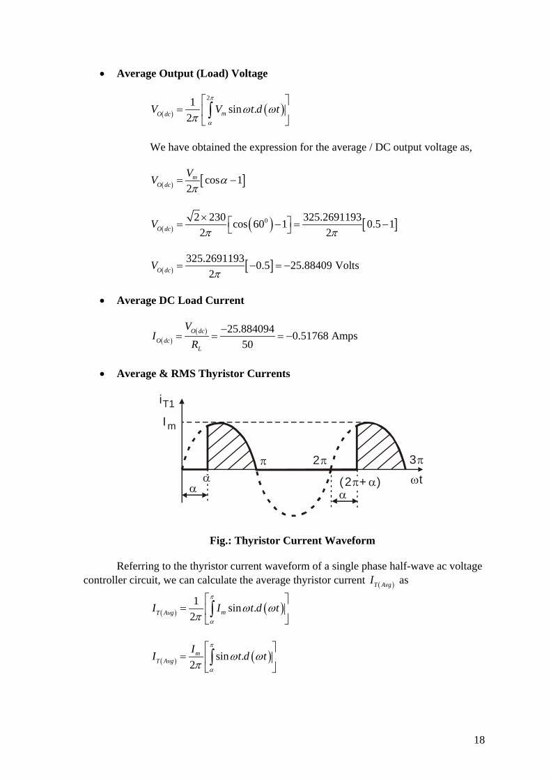
• Average & RMS Thyristor Currents
Im
iT1
π 2πα (2 + )π α
3π
α αωt
Fig.: Thyristor Current Waveform
Referring to the thyristor current waveform of a single phase half-wave ac voltage controller circuit, we can calculate the average thyristor current ( )T AvgI as
( ) ( )1 sin .2 mT AvgI I t d t
π
α
ω ωπ
=
∫
( ) ( )sin .2
mT Avg
II t d tπ
α
ω ωπ
=
∫

19
( ) ( )cos2
mT Avg
II tπ
α
ωπ
= −
( ) ( )cos cos2
mT Avg
II π απ
= − +
( ) [ ]1 cos2
mT Avg
II απ
= +
Where, mm
L
VIR
= = Peak thyristor current = Peak load current.
2 23050mI ×
=
6.505382 AmpsmI =
( ) [ ]1 cos2
mT Avg
L
VIR
απ
= +
( ) ( )02 230 1 cos 602 50T AvgIπ
× = + ×
( ) [ ]2 230 1 0.5100T AvgI
π×
= +
( ) 1.5530 AmpsT AvgI =
• RMS thyristor current ( )T RMSI can be calculated by using the expression
( ) ( )2 21 sin .2 mT RMSI I t d t
π
α
ω ωπ
=
∫
( )( ) ( )
2 1 cos 2.
2 2m
T RMS
tII d tπ
α
ωω
π −
= ∫
( ) ( ) ( )2
cos 2 .4
mT RMS
II d t t d tπ π
α α
ω ω ωπ
= −
∫ ∫
( ) ( )1 sin 224mT RMS
tI I tπ π
α α
ωωπ
= −

20
( ) ( )1 sin 2 sin 24 2mT RMSI I π απ απ
− = − −
( ) ( )1 sin 24 2mT RMSI I απ απ
= − +
( ) ( )1 sin 22 22
mT RMS
II απ απ
= − +
( )( )0sin 1206.50538 1
2 3 22T RMSI πππ
= − +
( )1 2 0.86602544.6
2 3 2T RMSI ππ
= +
( ) 4.6 0.6342 2.91746T RMSI A= × =
( ) 2.91746 AmpsT RMSI =
SINGLE PHASE FULL WAVE AC VOLTAGE CONTROLLER (AC REGULATOR) OR RMS VOLTAGE CONTROLLER WITH RESISTIVE LOAD
Single phase full wave ac voltage controller circuit using two SCRs or a single
triac is generally used in most of the ac control applications. The ac power flow to the
load can be controlled in both the half cycles by varying the trigger angle ' 'α .
The RMS value of load voltage can be varied by varying the trigger angle ' 'α .
The input supply current is alternating in the case of a full wave ac voltage controller and
due to the symmetrical nature of the input supply current waveform there is no dc
component of input supply current i.e., the average value of the input supply current is
zero.
A single phase full wave ac voltage controller with a resistive load is shown in the
figure below. It is possible to control the ac power flow to the load in both the half cycles
by adjusting the trigger angle ' 'α . Hence the full wave ac voltage controller is also
referred to as to a bi-directional controller.
21
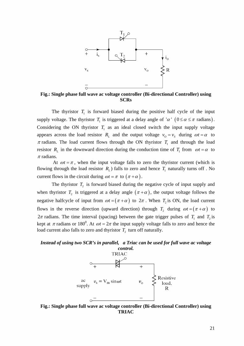
Fig.: Single phase full wave ac voltage controller (Bi-directional Controller) using SCRs
The thyristor 1T is forward biased during the positive half cycle of the input supply voltage. The thyristor 1T is triggered at a delay angle of ' 'α ( )0 radiansα π≤ ≤ . Considering the ON thyristor 1T as an ideal closed switch the input supply voltage appears across the load resistor LR and the output voltage O Sv v= during tω α= to π radians. The load current flows through the ON thyristor 1T and through the load resistor LR in the downward direction during the conduction time of 1T from tω α= to π radians.
At tω π= , when the input voltage falls to zero the thyristor current (which is flowing through the load resistor LR ) falls to zero and hence 1T naturally turns off . No current flows in the circuit during tω π= to ( )π α+ .
The thyristor 2T is forward biased during the negative cycle of input supply and when thyristor 2T is triggered at a delay angle ( )π α+ , the output voltage follows the
negative halfcycle of input from ( )tω π α= + to 2π . When 2T is ON, the load current
flows in the reverse direction (upward direction) through 2T during ( )tω π α= + to 2π radians. The time interval (spacing) between the gate trigger pulses of 1T and 2T is kept at π radians or 1800. At 2tω π= the input supply voltage falls to zero and hence the load current also falls to zero and thyristor 2T turn off naturally.
Instead of using two SCR’s in parallel, a Triac can be used for full wave ac voltage control.
Fig.: Single phase full wave ac voltage controller (Bi-directional Controller) using TRIAC

22
Fig: Waveforms of single phase full wave ac voltage controller
EQUATIONS Input supply voltage
sin 2 sinS m Sv V t V tω ω= = ;
Output voltage across the load resistor LR ; sinO L mv v V tω= = ;
for to tω α π= and ( ) to 2tω π α π= +
Output load current sin sinO m
O mL L
v V ti I tR R
ω ω= = = ;
for to tω α π= and ( ) to 2tω π α π= +
TO DERIVE AN EXPRESSION FOR THE RMS VALUE OF OUTPUT (LOAD) VOLTAGE
The RMS value of output voltage (load voltage) can be found using the expression
( ) ( ) ( )2
2 2 2
0
12 LO RMS L RMSV V v d t
π
ωπ
= = ∫ ;

23
For a full wave ac voltage controller, we can see that the two half cycles of output voltage waveforms are symmetrical and the output pulse time period (or output pulse repetition time) is π radians. Hence we can also calculate the RMS output voltage by using the expression given below.
( )2 2 2
0
1 sin .mL RMSV V t d tπ
ω ωπ
= ∫
( ) ( )2
2 2
0
1 .2 LL RMSV v d t
π
ωπ
= ∫ ;
sinL O mv v V tω= = ; For to tω α π= and ( ) to 2tω π α π= +
Hence,
( ) ( ) ( ) ( ) ( )2
2 22 1 sin sin2 m mL RMSV V t d t V t d t
π π
α π α
ω ω ω ωπ +
= +
∫ ∫
( ) ( )2
2 2 2 21 sin . sin .2 m mV t d t V t d t
π π
α π α
ω ω ω ωπ +
= +
∫ ∫
( ) ( )22 1 cos 2 1 cos 2
2 2 2mV t td t d t
π π
α π α
ω ωω ωπ +
− −= +
∫ ∫
( ) ( ) ( ) ( )2 22
cos 2 . cos 2 .2 2
mV d t t d t d t t d tπ π π π
α α π α π α
ω ω ω ω ω ωπ + +
= − + − ×
∫ ∫ ∫ ∫
( ) ( )2 22 sin 2 sin 2
4 2 2mV t tt t
π π π π
α π α α π α
ω ωω ωπ + +
= + − −
( ) ( ) ( ) ( )( )2 1 1sin 2 sin 2 sin 4 sin 2
4 2 2mV π α π α π α π π απ
= − + − − − − − +
( ) ( ) ( )( )2 1 12 0 sin 2 0 sin 2
4 2 2mV π α α π απ
= − − − − − +
( ) ( )2 sin 2sin 224 2 2
mV π ααπ απ
+ = − + +
( ) ( )2 sin 2 2sin 224 2 2
mV π ααπ απ
+ = − + +

24
( ) ( )2 sin 2 12 sin 2 .cos 2 cos 2 .sin 2
4 2 2mV απ α π α π απ
= − + + +
sin 2 0 & cos 2 1π π= =
Therefore,
( ) ( )2
2 sin 2 sin 224 2 2
mL RMS
VV α απ απ
= − + +
( )2
2 sin 24
mV π α απ
= − +
( ) ( )2
2 2 2 sin 24
mL RMS
VV π α απ
= − +
Taking the square root, we get
( ) ( )2 2 sin 22
mL RMS
VV π α απ
= − +
( ) ( )2 2 sin 22 2
mL RMS
VV π α απ
= − +
( ) ( )1 2 2 sin 222
mL RMS
VV π α απ
= − +
( ) ( )1 sin 222 22
mL RMS
VV απ απ
= − +
( ) ( )1 sin 222
mL RMS
VV απ απ
= − +
( ) ( ) ( )1 sin 22L RMS i RMSV V απ α
π = − +
( ) ( )1 sin 22SL RMSV V απ α
π = − +
Maximum RMS voltage will be applied to the load when 0α = , in that case the full sine wave appears across the load. RMS load voltage will be the same as the RMS
supply voltage 2mV
= . When α is increased the RMS load voltage decreases.

25
( ) ( )0
1 sin 2 0022
mL RMS
VVα
ππ=
× = − +
( ) ( )0
1 022
mL RMS
VVα
ππ=
= +
( ) ( )0 2
mSL RMS i RMS
VV V Vα =
= = =
The output control characteristic for a single phase full wave ac voltage controller with resistive load can be obtained by plotting the equation for ( )O RMSV
CONTROL CHARACTERISTIC OF SINGLE PHASE FULL-WAVE AC VOLTAGE CONTROLLER WITH RESISTIVE LOAD
The control characteristic is the plot of RMS output voltage ( )O RMSV versus the trigger angle α ; which can be obtained by using the expression for the RMS output voltage of a full-wave ac controller with resistive load.
( ) ( )1 sin 22SO RMSV V απ α
π = − +
;
Where 2m
SVV = = RMS value of input supply voltage
Trigger angle α in degrees
Trigger angle α in radians ( )O RMSV %
0 0 SV 100% SV030 6
π ( )1; 6π 0.985477 SV 98.54% SV
060 3π ( )2; 6
π 0.896938 SV 89.69% SV
090 2π ( )3; 6
π 0.7071 SV 70.7% SV
0120 23
π ( )4; 6π 0.44215 SV 44.21% SV
0150 56
π ( )5; 6π 0.1698 SV 16.98% SV
0180 π ( )6; 6π 0 SV 0 SV

26
VO(RMS)
Trigger angle in degreesα
0 60 120 180
VS
0.2 VS
0.6VS
We can notice from the figure, that we obtain a much better output control characteristic by using a single phase full wave ac voltage controller. The RMS output voltage can be varied from a maximum of 100% SV at 0α = to a minimum of ‘0’ at
0180α = . Thus we get a full range output voltage control by using a single phase full wave ac voltage controller.
Need For Isolation In the single phase full wave ac voltage controller circuit using two SCRs or
Thyristors 1T and 2T in parallel, the gating circuits (gate trigger pulse generating circuits) of Thyristors 1T and 2T must be isolated. Figure shows a pulse transformer with two separate windings to provide isolation between the gating signals of 1T and 2T .
G1
K1G2
K2
GateTriggerPulse
Generator
Fig.: Pulse Transformer
SINGLE PHASE FULL-WAVE AC VOLTAGE CONTROLLER WITH COMMON CATHODE
It is possible to design a single phase full wave ac controller with a common cathode configuration by having a common cathode point for 1T and 2T & by adding two diodes in a full wave ac controller circuit as shown in the figure below

27
Fig.: Single phase full wave ac controller with common cathode (Bidirectional controller in common cathode configuration)
Thyristor 1T and diode 1D are forward biased during the positive half cycle of input supply. When thyristor 1T is triggered at a delay angle α , Thyristor 1T and diode
1D conduct together from tω α= to π during the positive half cycle. The thyristor 2T and diode 2D are forward biased during the negative half cycle
of input supply, when trigged at a delay angle α , thyristor 2T and diode 2D conduct together during the negative half cycle from ( )tω π α= + to 2π .
In this circuit as there is one single common cathode point, routing of the gate trigger pulses to the thyristor gates of 1T and 2T is simpler and only one isolation circuit is required.
But due to the need of two power diodes the costs of the devices increase. As there are two power devices conducting at the same time the voltage drop across the ON devices increases and the ON state conducting losses of devices increase and hence the efficiency decreases.
SINGLE PHASE FULL WAVE AC VOLTAGE CONTROLLER USING A SINGLE THYRISTOR
RL
T1
ACSupply
-
D1
D4
D3
D2
+

28
A single phase full wave ac controller can also be implemented with one thyristor and four diodes connected in a full wave bridge configuration as shown in the above figure. The four diodes act as a bridge full wave rectifier. The voltage across the thyristor
1T and current through thyristor 1T are always unidirectional. When 1T is triggered at tω α= , during the positive half cycle ( )0 α π≤ ≤ , the load current flows through 1D , 1T ,
diode 2D and through the load. With a resistive load, the thyristor current (flowing through the ON thyristor 1T ) , the load current falls to zero at tω π= , when the input supply voltage decreases to zero at tω π= , the thyristor naturally turns OFF.
In the negative half cycle, diodes 3 4&D D are forward biased during to 2tω π π= radians. When 1T is triggered at ( )tω π α= + , the load current flows in the
opposite direction (upward direction) through the load, through 3D , 1T and 4D . Thus 3D ,
4D and 1T conduct together during the negative half cycle to supply the load power. When the input supply voltage becomes zero at 2tω π= , the thyristor current (load current) falls to zero at 2tω π= and the thyristor 1T naturally turns OFF. The waveforms and the expression for the RMS output voltage are the same as discussed earlier for the single phase full wave ac controller.
But however if there is a large inductance in the load circuit, thyristor 1T may not be turned OFF at the zero crossing points, in every half cycle of input voltage and this may result in a loss of output control. This would require detection of the zero crossing of the load current waveform in order to ensure guaranteed turn off of the conducting thyristor before triggering the thyristor in the next half cycle, so that we gain control on the output voltage.
In this full wave ac controller circuit using a single thyristor, as there are three power devices conducting together at the same time there is more conduction voltage drop and an increase in the ON state conduction losses and hence efficiency is also reduced.
The diode bridge rectifier and thyristor (or a power transistor) act together as a
bidirectional switch which is commercially available as a single device module and it has
relatively low ON state conduction loss. It can be used for bidirectional load current
control and for controlling the RMS output voltage.
SINGLE PHASE FULL WAVE AC VOLTAGE CONTROLLER (BIDIRECTIONAL CONTROLLER) WITH RL LOAD
In this section we will discuss the operation and performance of a single phase full
wave ac voltage controller with RL load. In practice most of the loads are of RL type. For
example if we consider a single phase full wave ac voltage controller controlling the
speed of a single phase ac induction motor, the load which is the induction motor winding
is an RL type of load, where R represents the motor winding resistance and L represents
the motor winding inductance.

29
A single phase full wave ac voltage controller circuit (bidirectional controller)
with an RL load using two thyristors 1T and 2T ( 1T and 2T are two SCRs) connected in
parallel is shown in the figure below. In place of two thyristors a single Triac can be used
to implement a full wave ac controller, if a suitable Traic is available for the desired RMS
load current and the RMS output voltage ratings.
Fig: Single phase full wave ac voltage controller with RL load
The thyristor 1T is forward biased during the positive half cycle of input supply.
Let us assume that 1T is triggered at tω α= , by applying a suitable gate trigger pulse to
1T during the positive half cycle of input supply. The output voltage across the load
follows the input supply voltage when 1T is ON. The load current Oi flows through the
thyristor 1T and through the load in the downward direction. This load current pulse
flowing through 1T can be considered as the positive current pulse. Due to the inductance
in the load, the load current Oi flowing through 1T would not fall to zero at tω π= , when
the input supply voltage starts to become negative.
The thyristor 1T will continue to conduct the load current until all the inductive
energy stored in the load inductor L is completely utilized and the load current through 1T
falls to zero at tω β= , where β is referred to as the Extinction angle, (the value of tω )
at which the load current falls to zero. The extinction angle β is measured from the point
of the beginning of the positive half cycle of input supply to the point where the load
current falls to zero.

30
The thyristor 1T conducts from tω α= to β . The conduction angle of 1T is
( )δ β α= − , which depends on the delay angle α and the load impedance angle φ . The
waveforms of the input supply voltage, the gate trigger pulses of 1T and 2T , the thyristor
current, the load current and the load voltage waveforms appear as shown in the figure
below.
Fig.: Input supply voltage & Thyristor current waveforms
β is the extinction angle which depends upon the load inductance value.
Fig.: Gating Signals

31
Waveforms of single phase full wave ac voltage controller with RL load for α φ> . Discontinuous load current operation occurs for α φ> and β (< +π α ) ; i.e., (β α )− <π , conduction angle <π .
Fig.: Waveforms of Input supply voltage, Load Current, Load Voltage and Thyristor Voltage across 1T
Note • The RMS value of the output voltage and the load current may be varied by
varying the trigger angle α .• This circuit, AC RMS voltage controller can be used to regulate the RMS voltage
across the terminals of an ac motor (induction motor). It can be used to control thetemperature of a furnace by varying the RMS output voltage.

32
• For very large load inductance ‘L’ the SCR may fail to commutate, after it istriggered and the load voltage will be a full sine wave (similar to the applied inputsupply voltage and the output control will be lost) as long as the gating signals areapplied to the thyristors 1T and 2T . The load current waveform will appear as a full continuous sine wave and the load current waveform lags behind the output sine wave by the load power factor angle φ.
TO DERIVE AN EXPRESSION FOR THE OUTPUT (INDUCTIVE LOAD) CURRENT, DURING to tω α β= WHEN THYRISTOR 1T CONDUCTS
Considering sinusoidal input supply voltage we can write the expression for the supply voltage as
sinS mv V tω= = instantaneous value of the input supply voltage.
Let us assume that the thyristor 1T is triggered by applying the gating signal to 1T at tω α= . The load current which flows through the thyristor 1T during tω α= to β can be found from the equation
sinOO m
diL Ri V tdt
ω + =
;
The solution of the above differential equation gives the general expression for the output load current which is of the form
( ) 1sint
mO
Vi t A eZ
τω φ−
= − + ;
Where 2m SV V= = maximum or peak value of input supply voltage.
( )22Z R Lω= + = Load impedance.
1tan LR
ωφ − =
= Load impedance angle (power factor angle of load).
LR
τ = = Load circuit time constant.
Therefore the general expression for the output load current is given by the equation
( )
1sinR tm L
OVi t A eZ
ω φ−
= − + ;

33
The value of the constant 1A can be determined from the initial condition. i.e. initial value of load current 0Oi = , at tω α= . Hence from the equation for Oi equating
Oi to zero and substituting tω α= , we get
( )
10 sinR tm L
OVi A eZ
α φ−
= = − +
Therefore ( )1 sinRt mL VA e
Zα φ
− −= −
( )11 sinm
RtL
VAZe
α φ−
− = −
( )1 sinRt mL VA e
Zα φ
+ − = −
( )
( )1 sinR t
mL VA eZ
ωω α φ− = −
By substituting tω α= , we get the value of constant 1A as
( )
( )1 sinR
mL VA eZ
αω α φ− = −
Substituting the value of constant 1A from the above equation into the expression for Oi , we obtain
( )( )
( )sin sinRRtm mLL
OV Vi t e eZ Z
αωω φ α φ
− − = − + − ;
( )( ) ( )
( )sin sinR t R
m mL LO
V Vi t e eZ Z
ω αω ωω φ α φ
− − = − + −
( ) ( ) ( )sin sinR tm mL
OV Vi t eZ Z
ω αωω φ α φ−
− − = − + −
Therefore we obtain the final expression for the inductive load current of a single phase full wave ac voltage controller with RL load as
( ) ( ) ( )sin sin
R tm LO
Vi t eZ
ω αωω φ α φ−
− = − − −
; Where tα ω β≤ ≤ .
34
The above expression also represents the thyristor current 1Ti , during the conduction time interval of thyristor 1T from to tω α β= .
To Calculate Extinction Angle β The extinction angle β , which is the value of tω at which the load current
Oi falls to zero and 1T is turned off can be estimated by using the condition that 0Oi = , at tω β=
By using the above expression for the output load current, we can write
( ) ( ) ( )0 sin sin
Rm L
OVi eZ
β αωβ φ α φ−
− = = − − −
As 0mVZ
≠ we can write
( ) ( ) ( )sin sin 0
RLe
β αωβ φ α φ−
− − − − =
Therefore we obtain the expression
( ) ( ) ( )sin sin
RLe
β αωβ φ α φ−
−− = −
The extinction angle β can be determined from this transcendental equation by using the iterative method of solution (trial and error method). After β is calculated, we can determine the thyristor conduction angle ( )δ β α= − .
β is the extinction angle which depends upon the load inductance value. Conduction angle δ increases as α is decreased for a known value of β .
For δ π< radians, i.e., for ( )β α π− < radians, for ( )π α β+ > the load current waveform appears as a discontinuous current waveform as shown in the figure. The output load current remains at zero during tω β= to ( )π α+ . This is referred to as
discontinuous load current operation which occurs for ( )β π α< + . When the trigger angle α is decreased and made equal to the load impedance
angle φ i.e., when α φ= we obtain from the expression for ( )sin β φ− ,
( )sin 0β φ− = ; Therefore ( )β φ π− = radians.
Extinction angle ( ) ( )β π φ π α= + = + ; for the case when α φ=
Conduction angle ( ) 0 radians 180δ β α π= − = = ; for the case when α φ=
Each thyristor conducts for 1800 ( radiansπ ) . 1T conducts from tω φ= to
( )π φ+ and provides a positive load current. 2T conducts from ( )π φ+ to ( )2π φ+ and provides a negative load current. Hence we obtain a continuous load current and the

35
output voltage waveform appears as a continuous sine wave identical to the input supply voltage waveform for trigger angle α φ≤ and the control on the output is lost.
vO
π 2πφ
3π
φ
ωt
Vm
0
φ φ
Im
ωtφ
v =vO S
iO
Fig.: Output voltage and output current waveforms for a single phase full wave ac voltage controller with RL load for α φ≤
Thus we observe that for trigger angle α φ≤ , the load current tends to flow continuously and we have continuous load current operation, without any break in the load current waveform and we obtain output voltage waveform which is a continuous sinusoidal waveform identical to the input supply voltage waveform. We loose the control on the output voltage for α φ≤ as the output voltage becomes equal to the input supply voltage and thus we obtain
( ) 2m
SO RMSVV V= = ; for α φ≤
Hence, RMS output voltage = RMS input supply voltage for α φ≤
TO DERIVE AN EXPRESSION FOR RMS OUTPUT VOLTAGE ( )O RMSV OF A SINGLE PHASE FULL-WAVE AC VOLTAGE CONTROLLER WITH RL LOAD.

36
Whenα > O , the load current and load voltage waveforms become discontinuous as shown in the figure above.
( ) ( )12
2 21 sin .mO RMSV V t d tβ
α
ω ωπ
=
∫
Output sino mv V tω= , for to tω α β= , when 1T is ON.
( )( ) ( )
122 1 cos 2
2m
O RMS
tVV d tβ
α
ωω
π −
=
∫
( ) ( ) ( )1
22
cos 2 .2
mO RMS
VV d t t d tβ β
α α
ω ω ωπ
= − ∫ ∫
( ) ( )1
22 sin 222
mO RMS
V tV tβ β
α α
ωωπ
= −
( ) ( )1
2 2sin 2 sin 22 2 2
mO RMS
VV β αβ απ
= − − +
( ) ( )1
21 sin 2 sin 22 2 2mO RMSV V α ββ απ
= − + −
( ) ( )1
21 sin 2 sin 22 22
mO RMS
VV α ββ απ
= − + −
The RMS output voltage across the load can be varied by changing the trigger angle α .
For a purely resistive load 0L = , therefore load power factor angle 0φ = . 1tan 0L
Rωφ − = =
;
Extinction angle 0 radians 180β π= =

37
PERFORMANCE PARAMETERS OF A SINGLE PHASE FULL WAVE AC VOLTAGE CONTROLLER WITH RESISTIVE LOAD
• RMS Output Voltage ( ) ( )1 sin 222
mO RMS
VV απ απ
= − + ;
2m
SV V= = RMS
input supply voltage.
• ( )( )O RMS
O RMSL
VI
R= = RMS value of load current.
• ( )S O RMSI I= = RMS value of input supply current.
• Output load power( )
2O LO RMSP I R= ×
• Input Power Factor
( )
( )
( )2
L LO RMS O RMSO
S S S SO RMS
I R I RPPFV I V I V
× ×= = =
× ×
( ) ( )1 sin 22
O RMS
S
VPF
Vαπ α
π = = − +
• Average Thyristor Current,
Im
iT1
π 2πα (2 + )π α
3π
α αωt
Fig.: Thyristor Current Waveform
( ) ( ) ( )1 1 sin .2 2T mT AvgI i d t I t d t
π π
α α
ω ω ωπ π
= =∫ ∫
( ) ( )sin . cos2 2
m mT Avg
I II t d t tπ π
αα
ω ω ωπ π
= = −
∫
( ) [ ] [ ]cos cos 1 cos2 2
m mT Avg
I II π α απ π
= − + = +

38
• Maximum Average Thyristor Current, for 0α = ,
( )m
T AvgIIπ
=
• RMS Thyristor Current
( ) ( )2 21 sin .2 mT RMSI I t d t
π
α
ω ωπ
=
∫
( ) ( )1 sin 22 22
mT RMS
II απ απ
= − +
• Maximum RMS Thyristor Current, for 0α = ,
( ) 2m
T RMSII =
In the case of a single phase full wave ac voltage controller circuit using a Triac with resistive load, the average thyristor current ( ) 0T AvgI = . Because the Triac conducts in both the half cycles and the thyristor current is alternating and we obtain a symmetrical thyristor current waveform which gives an average value of zero on integration.
PERFORMANCE PARAMETERS OF A SINGLE PHASE FULL WAVE AC VOLTAGE CONTROLLER WITH R-L LOAD
The Expression for the Output (Load) Current The expression for the output (load) current which flows through the thyristor,
during to tω α β= is given by
( ) ( ) ( )1
sin sinR tm L
O TVi i t eZ
ω αωω φ α φ−
− = = − − −
; for tα ω β≤ ≤
Where, 2m SV V= = Maximum or peak value of input ac supply voltage.
( )22Z R Lω= + = Load impedance.
1tan LR
ωφ − =
= Load impedance angle (load power factor angle).
α = Thyristor trigger angle = Delay angle.
β = Extinction angle of thyristor, (value of tω ) at which the thyristor (load) current falls to zero.
β is calculated by solving the equation
( ) ( ) ( )sin sin
RLe
β αωβ φ α φ−
−− = −
39
Thyristor Conduction Angle ( )δ β α= −
Maximum thyristor conduction angle ( )δ β α π= − = radians = 1800 for α φ≤ .
RMS Output Voltage
( ) ( )1 sin 2 sin 22 22
mO RMS
VV α ββ απ
= − + −
The Average Thyristor Current
( ) ( )1
12 TT AvgI i d t
β
α
ωπ
=
∫
( ) ( ) ( ) ( ) ( )1 sin sin2
R tm LT Avg
VI t e d tZ
βω α
ω
α
ω φ α φ ωπ
−−
= − − − ∫
( ) ( ) ( ) ( ) ( ) ( )sin . sin2
R tm LT Avg
VI t d t e d tZ
β βω α
ω
α α
ω φ ω α φ ωπ
−−
= − − − ∫ ∫
Maximum value of ( )T AvgI occur at 0α = . The thyristors should be rated for
maximum ( )m
T AvgIIπ
=
, where mm
VIZ
= .
RMS Thyristor Current ( )T RMSI
( ) ( )1
212 TT RMSI i d t
β
α
ωπ
=
∫
Maximum value of ( )T RMSI occurs at 0α = . Thyristors should be rated for
maximum ( ) 2m
T RMSII =
When a Triac is used in a single phase full wave ac voltage controller with RL
type of load, then ( ) 0T AvgI = and maximum ( ) 2m
T RMSII =

40
PROBLEMS
1. A single phase full wave ac voltage controller supplies an RL load. The inputsupply voltage is 230V, RMS at 50Hz. The load has L = 10mH, R = 10Ω, the
delay angle of thyristors 1T and 2T are equal, where 1 2 3πα α= = . Determine
a. Conduction angle of the thyristor 1T .b. RMS output voltage.c. The input power factor.
Comment on the type of operation.Given
230sV V= , 50f Hz= , 10L mH= , 10R = Ω , 060α = ,
1 2 3πα α α= = = radians, .
2 2 230 325.2691193 m SV V V= = × =
( ) ( ) ( )2 2 22 Load Impedance 10Z R L Lω ω= = + = +
( ) ( )32 2 50 10 10 3.14159L fLω π π π−= = × × × = = Ω
( ) ( )2 210 3.14159 109.8696 10.4818Z = + = = Ω
2 230 31.03179 10.4818
mm
VI AZ
×= = =
Load Impedance Angle 1tan LR
ωφ − =
( )1 1 0tan tan 0.314159 17.4405910πφ − − = = =
Trigger Angle α φ> . Hence the type of operation will be discontinuous load current operation, we get
( )β π α< +
( )180 60β < + ; 0240β <
Therefore the range of β is from 180 degrees to 240 degrees.
( )0 0180 240β< <

41
Extinction Angle β is calculated by using the equation
( ) ( ) ( )sin sin
RLe
β αωβ φ α φ−
−− = −
In the exponential term the value of α and β should be substituted in radians. Hence
( ) ( ) ( )sin sin Rad Rad
RLe
β αωβ φ α φ−
−− = − ;
3Radπα =
( ) ( ) 060 17.44059 42.5594α φ− = − =
( ) ( ) ( )100 0sin 17.44 sin 42.5594 e
β απβ
−−
− =
( ) ( )0 3.183sin 17.44 0.676354e β αβ − −− =
0180 radians, π→0
0180Radβ πβ ×
=
Assuming 0190β = ; 0 0
0
190 3.3161180 180Radβ π πβ × ×
= = =
L.H.S: ( ) ( )0sin 190 17.44 sin 172.56 0.129487− = =
R.H.S: 3.183 3.3161
430.676354 4.94 10eπ − − − × = ×
Assuming 0183β = ; 0 0
0
183 3.19395180 180Radβ π πβ × ×
= = =
( ) 3.19395 2.146753πβ α − = − =
L.H.S: ( ) ( ) 0sin sin 183 17.44 sin165.56 0.24936β φ− = − = =
R.H.S: ( )3.183 2.14675 40.676354 7.2876 10e− −= ×
Assuming 0180β ≈ 0 0
0
180180 180Radβ π πβ π× ×
= = =
( ) 23 3π πβ α π − = − =
42
L.H.S: ( ) ( )sin sin 180 17.44 0.2997β φ− = − =
R.H.S: 3.183
430.676354 8.6092 10eππ − − − = ×
Assuming 0196β = 0 0
0
196 3.420845180 180Radβ π πβ × ×
= = =
L.H.S: ( ) ( )sin sin 196 17.44 0.02513β φ− = − =
R.H.S: 3.183 3.420845
430.676354 3.5394 10eπ − − − = ×
Assuming 0197β = 0 0
0
197 3.43829180 180Radβ π πβ × ×
= = =
L.H.S: ( ) ( ) 3sin sin 197 17.44 7.69 7.67937 10β φ −− = − = = ×
R.H.S: 3.183 3.43829
430.676354 4.950386476 10eπ − − − = ×
Assuming 0197.42β = 0
0
197.42 3.4456180 180Radβ π πβ × ×
= = =
L.H.S: ( ) ( ) 4sin sin 197.42 17.44 3.4906 10β φ −− = − = ×
R.H.S: 3.183 3.4456
430.676354 3.2709 10eπ − − − = ×
Conduction Angle ( ) ( )0 0 0197.42 60 137.42δ β α= − = − =
RMS Output Voltage
( ) ( )1 sin 2 sin 22 2SO RMSV V α ββ α
π = − + −
( )( ) ( )0 0sin 2 60 sin 2 197.421230 3.4456
3 2 2O RMSV ππ
= − + −
( ) ( )1230 2.39843 0.4330 0.285640O RMSVπ
= + −
( ) 230 0.9 207.0445 VO RMSV = × =

43
Input Power Factor O
S S
PPFV I
=×
( )( ) 207.0445 19.7527 A
10.4818O RMS
O RMS
VI
Z= = =
( ) ( )22 19.7527 10 3901.716 WO LO RMSP I R= × = × =
( )230 , 19.7527S S O RMSV V I I= = =
3901.716 0.8588230 19.7527
O
S S
PPFV I
= = =× ×
2. A single phase full wave controller has an input voltage of 120 V (RMS) and aload resistance of 6 ohm. The firing angle of thyristor is 2π . Find
a. RMS output voltageb. Power outputc. Input power factord. Average and RMS thyristor current.
Solution 090 , 120 V, 6
2 SV Rπα = = = = Ω
RMS Value of Output Voltage 121 sin 2
2O SV V απ απ
= − +
121 sin180120
2 2OV πππ
= − +
84.85 VoltsOV =
RMS Output Current
84.85 14.14 A6
OO
VIR
= = =
Load Power 2
O OP I R= ×
( )214.14 6 1200 wattsOP = × =

44
Input Current is same as Load Current Therefore 14.14 AmpsS OI I= = Input Supply Volt-Amp 120 14.14 1696.8 S SV I VA= = × =
Therefore
Input Power Factor = ( )Load Power 1200 0.707Input Volt-Amp 1696.8
lag= =
Each Thyristor Conducts only for half a cycle
Average thyristor current ( )T AvgI
( ) ( )1 sin .2 mT AvgI V t d t
R
π
α
ω ωπ
= ∫
( ) m1 cos ; V 22
mS
V VR
απ
= + =
[ ]2 120 1 cos90 4.5 A2 6π
×= + =
×
RMS thyristor current ( )T RMSI
( ) ( )2 2
2
sin12
mT RMS
V tI d tR
π
α
ω ωπ
= ∫
( ) ( )2
2
1 cos 22 2
m tV d tR
π
α
ωω
π−
= ∫
121 sin 2
2 2mVR
απ απ
= − +
122 1 sin 2
2 2SV
Rαπ α
π = − +
122 120 1 sin180 10 Amps
2 6 2 2ππ
π× = − + = ×
45
3. A single phase half wave ac regulator using one SCR in anti-parallel with a diodefeeds 1 kW, 230 V heater. Find load power for a firing angle of 450.
Solution045 , 230 V
4 SVπα = = = ; 1 1000OP KW W= =
At standard rms supply voltage of 230V, the heater dissipates 1KW of output power
Therefore 2
O O OO O O
V V VP V IR R×
= × = =
Resistance of heater ( )22 230
52.91000
O
O
VRP
= = = Ω
RMS value of output voltage 121 sin 22
2 2O SV V απ απ
= − + ; for firing angle 045α =
121 sin 90230 2 224.7157 Volts
2 4 2OV πππ
= − + =
RMS value of output current 224.9 4.2479 Amps52.9
OO
VIR
= = =
Load Power ( )22 4.25 52.9 954.56 WattsO OP I R= × = × =
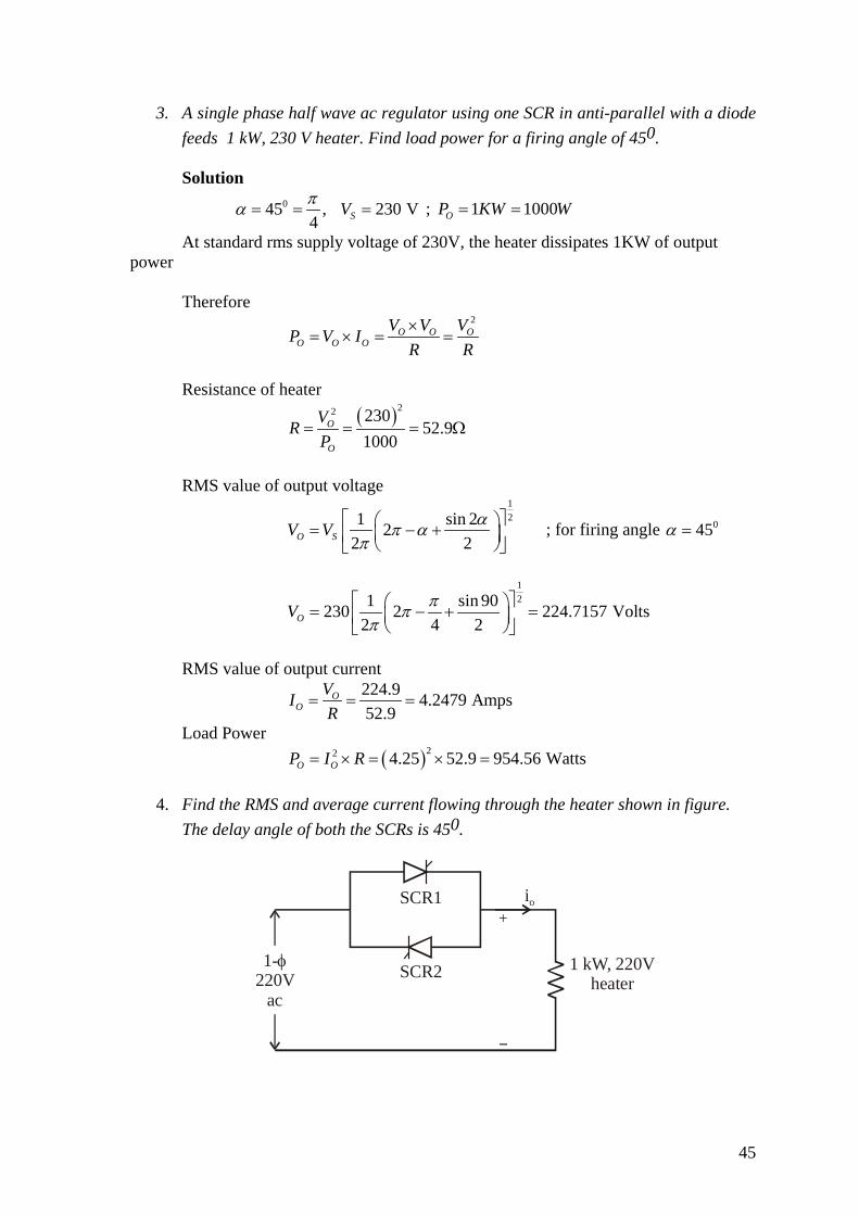
4. Find the RMS and average current flowing through the heater shown in figure.The delay angle of both the SCRs is 450.
SCR2
SCR1 io
+
1 kW, 220Vheater
1-220V
ac
φ

46
Solution 045 , 220 V
4 SVπα = = =
Resistance of heater ( )22 220
48.41000
VRR
= = = Ω
Resistance value of output voltage 1 sin 2
2O SV V απ απ
= − +
1 sin 902204 2OV ππ
π = − +
1 1220 209.769 Volts4 2OV ππ
π = − + =
RMS current flowing through heater 209.769 4.334 Amps48.4
OVR
= = =
Average current flowing through the heater 0AvgI =
5. A single phase voltage controller is employed for controlling the power flow from220 V, 50 Hz source into a load circuit consisting of R = 4 Ω and ωL = 6 Ω.Calculate the following
a. Control range of firing angleb. Maximum value of RMS load currentc. Maximum power and power factord. Maximum value of average and RMS thyristor current.
Solution
For control of output power, minimum angle of firing angle α is equal to the load impedance angle θ
, load angleα θ=
1 1 06tan tan 56.34
LR
ωθ − − = = =
Maximum possible value of α is 0180 Therefore control range of firing angle is 0 056.3 180α< <

47
Maximum value of RMS load current occurs when 056.3α θ= = . At this value of α the Maximum value of RMS load current
2 2
220 30.5085 Amps4 6
SO
VIZ
= = =+
Maximum Power ( )22 30.5085 4 3723.077 WO OP I R= = × =
Input Volt-Amp 220 30.5085 6711.87 WS OV I= = × =
Power Factor 3723.077 0.5547 6711.87
OPInput VA
= = =
Average thyristor current will be maximum when α θ= and conduction angle 0180γ = . Therefore maximum value of average thyristor current
( ) ( ) ( )1 sin2
mT Avg
VI t d tZ
π α
α
ω θ ωπ
+
= −∫
Note: ( ) ( ) ( )1
sin sinR tm L
O TVi i t eZ
ω αωω θ α θ−
− = = − − −
At 0α = ,
( )1
sinmT O
Vi i tZ
ω θ= = −
( ) ( )cos2
mT Avg
VI tZ
π α
αω θ
π+
= − −
( ) ( ) ( )cos cos2
mT Avg
VIZ
π α θ α θπ
= − + − + −
But α θ= ,
( ) ( ) ( ) [ ]cos cos 0 22 2
m m mT Avg
V V VIZ Z Z
ππ π π
= − + = =
( ) 2 2
2 220 13.7336 Amps4 6
mT Avg
VIZπ π
×∴ = = =
+
Similarly, maximum RMS value occurs when 0α = and γ π= .
Therefore maximum value of RMS thyristor current
( ) ( )21 sin
2m
TMVI t d tZ
π α
α
ω θ ωπ
+ = − ∫

48
( ) ( )2
2
1 cos 2 22 2
mTM
tVI d tZ
π α
α
ω θω
π
+ − − =
∫
( )2
2
sin 2 24 2
mTM
tVI tZ
π α
α
ω θω
π
+−
= −
[ ]2
2 04
mTM
VIZ
π α απ
= + − −
2 2
2 220 21.57277 Amps2 2 4 6
mTM
VIZ
×= = =
+
49
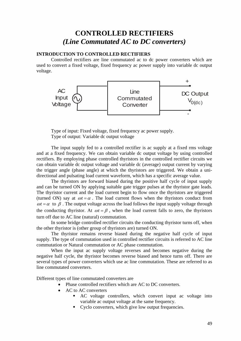
CONTROLLED RECTIFIERS (Line Commutated AC to DC converters)
INTRODUCTION TO CONTROLLED RECTIFIERS Controlled rectifiers are line commutated ac to dc power converters which are
used to convert a fixed voltage, fixed frequency ac power supply into variable dc output voltage.
LineCommutated
Converter
+
-
DC OutputV0(dc)
ACInput
Voltage
Type of input: Fixed voltage, fixed frequency ac power supply. Type of output: Variable dc output voltage
The input supply fed to a controlled rectifier is ac supply at a fixed rms voltage and at a fixed frequency. We can obtain variable dc output voltage by using controlled rectifiers. By employing phase controlled thyristors in the controlled rectifier circuits we can obtain variable dc output voltage and variable dc (average) output current by varying the trigger angle (phase angle) at which the thyristors are triggered. We obtain a uni-directional and pulsating load current waveform, which has a specific average value.
The thyristors are forward biased during the positive half cycle of input supply and can be turned ON by applying suitable gate trigger pulses at the thyristor gate leads. The thyristor current and the load current begin to flow once the thyristors are triggered (turned ON) say at tω α= . The load current flows when the thyristors conduct from
tω α= to β . The output voltage across the load follows the input supply voltage through the conducting thyristor. At tω β= , when the load current falls to zero, the thyristors turn off due to AC line (natural) commutation.
In some bridge controlled rectifier circuits the conducting thyristor turns off, when the other thyristor is (other group of thyristors are) turned ON.
The thyristor remains reverse biased during the negative half cycle of input supply. The type of commutation used in controlled rectifier circuits is referred to AC line commutation or Natural commutation or AC phase commutation.
When the input ac supply voltage reverses and becomes negative during the negative half cycle, the thyristor becomes reverse biased and hence turns off. There are several types of power converters which use ac line commutation. These are referred to as line commutated converters.
Different types of line commutated converters are • Phase controlled rectifiers which are AC to DC converters.• AC to AC converters
AC voltage controllers, which convert input ac voltage intovariable ac output voltage at the same frequency.
Cyclo converters, which give low output frequencies.

50
All these power converters operate from ac power supply at a fixed rms input supply voltage and at a fixed input supply frequency. Hence they use ac line commutation for turning off the thyristors after they have been triggered ON by the gating signals.
DIFFERENCES BETWEEN DIODE RECTIFIERS AND PHASE CONTROLLED RECTIFIERS
The diode rectifiers are referred to as uncontrolled rectifiers which make use of power semiconductor diodes to carry the load current. The diode rectifiers give a fixed dc output voltage (fixed average output voltage) and each diode rectifying element conducts for one half cycle duration (T/2 seconds), that is the diode conduction angle = 1800 or π radians.
A single phase half wave diode rectifier gives (under ideal conditions) an average
dc output voltage ( )m
O dcVVπ
= and single phase full wave diode rectifier gives (under ideal
conditions) an average dc output voltage ( )2 m
O dcVVπ
= , where mV is maximum value of
the available ac supply voltage. Thus we note that we can not control (we can not vary) the dc output voltage or
the average dc load current in a diode rectifier circuit. In a phase controlled rectifier circuit we use a high current and a high power
thyristor device (silicon controlled rectifier; SCR) for conversion of ac input power into dc output power.
Phase controlled rectifier circuits are used to provide a variable voltage output dc and a variable dc (average) load current.
We can control (we can vary) the average value (dc value) of the output load voltage (and hence the average dc load current) by varying the thyristor trigger angle.
We can control the thyristor conduction angle δ from 1800 to 00 by varying the trigger angle α from 00 to 1800, where thyristor conduction angle ( )δ π α= −
APPLICATIONS OF PHASE CONTROLLED RECTIFIERS • DC motor control in steel mills, paper and textile mills employing dc motor
drives.• AC fed traction system using dc traction motor.• Electro-chemical and electro-metallurgical processes.• Magnet power supplies.• Reactor controls.• Portable hand tool drives.• Variable speed industrial drives.• Battery charges.• High voltage DC transmission.• Uninterruptible power supply systems (UPS).
Some years back ac to dc power conversion was achieved using motor generatorsets, mercury arc rectifiers, and thyratorn tubes. The modern ac to dc power converters are designed using high power, high current thyristors and presently most of the ac-dc power converters are thyristorised power converters. The thyristor devices are phase controlled to obtain a variable dc output voltage across the output load terminals. The

51
phase controlled thyristor converter uses ac line commutation (natural commutation) for commutating (turning off) the thyristors that have been turned ON.
The phase controlled converters are simple and less expensive and are widely used in industrial applications for industrial dc drives. These converters are classified as two quadrant converters if the output voltage can be made either positive or negative for a given polarity of output load current. There are also single quadrant ac-dc converters where the output voltage is only positive and cannot be made negative for a given polarity of output current. Of course single quadrant converters can also be designed to provide only negative dc output voltage.
The two quadrant converter operation can be achieved by using fully controlled bridge converter circuit and for single quadrant operation we use a half controlled bridge converter.
CLASSIFICATION OF PHASE CONTROLLED RECTIFIERS The phase controlled rectifiers can be classified based on the type of input power
supply as • Single Phase Controlled Rectifiers which operate from single phase ac input
power supply.• Three Phase Controlled Rectifiers which operate from three phase ac input power
supply.
DIFFERENT TYPES OF SINGLE PHASE CONTROLLED RECTIFIERS Single Phase Controlled Rectifiers are further subdivided into different types
• Half wave controlled rectifier which uses a single thyristor device (whichprovides output control only in one half cycle of input ac supply, and it provideslow dc output).
• Full wave controlled rectifiers (which provide higher dc output)o Full wave controlled rectifier using a center tapped transformer (which
requires two thyristors).o Full wave bridge controlled rectifiers (which do not require a center tapped
transformer) Single phase semi-converter (half controlled bridge converter,
using two SCR’s and two diodes, to provide single quadrantoperation).
Single phase full converter (fully controlled bridge converter whichrequires four SCR’s, to provide two quadrant operation).
Three Phase Controlled Rectifiers are of different types • Three phase half wave controlled rectifiers.• Three phase full wave controlled rectiriers.
o Semi converter (half controlled bridge converter).o Full converter (fully controlled bridge converter).
PRINCIPLE OF PHASE CONTROLLED RECTIFIER OPERATION The basic principle of operation of a phase controlled rectifier circuit is explained
with reference to a single phase half wave phase controlled rectifier circuit with a resistive load shown in the figure.
52
Load ResistanceLR R= =
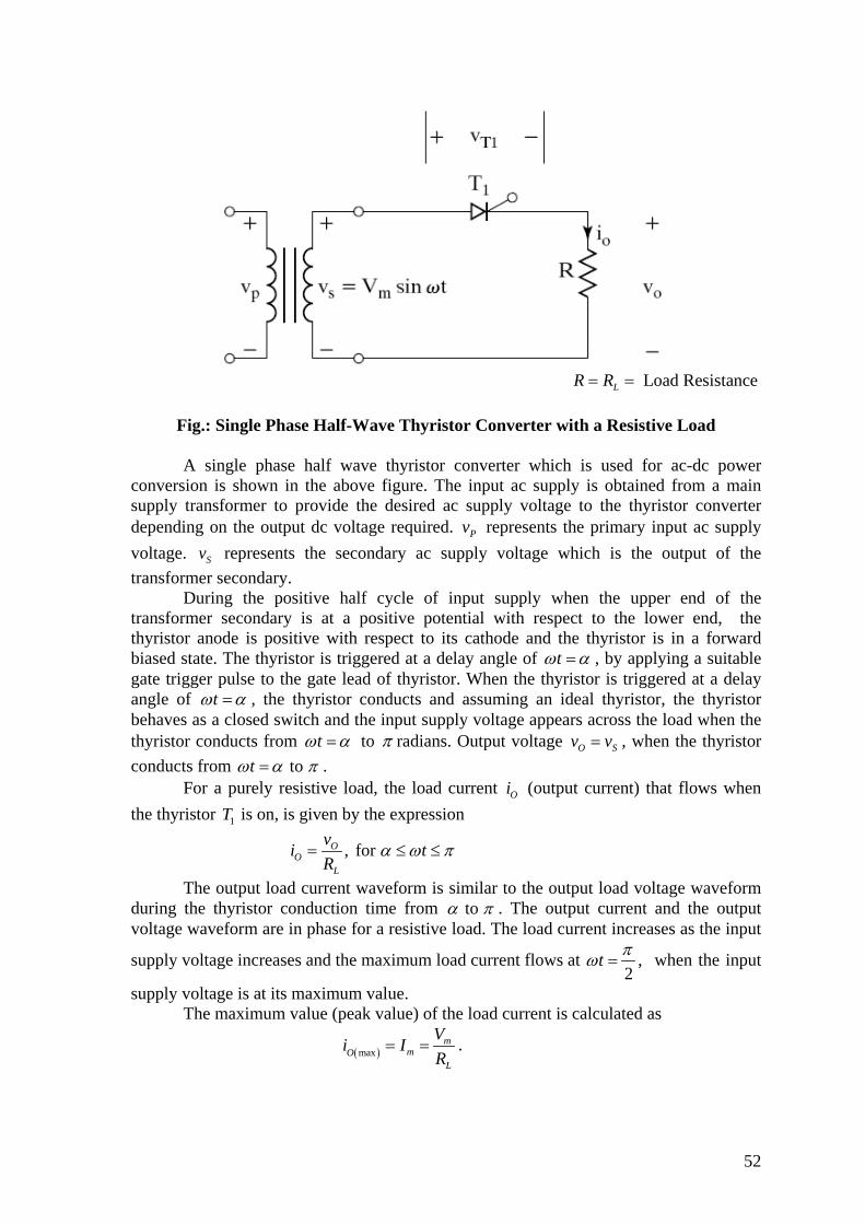
Fig.: Single Phase Half-Wave Thyristor Converter with a Resistive Load
A single phase half wave thyristor converter which is used for ac-dc power conversion is shown in the above figure. The input ac supply is obtained from a main supply transformer to provide the desired ac supply voltage to the thyristor converter depending on the output dc voltage required. Pv represents the primary input ac supply voltage. Sv represents the secondary ac supply voltage which is the output of the transformer secondary.
During the positive half cycle of input supply when the upper end of the transformer secondary is at a positive potential with respect to the lower end, the thyristor anode is positive with respect to its cathode and the thyristor is in a forward biased state. The thyristor is triggered at a delay angle of tω α= , by applying a suitable gate trigger pulse to the gate lead of thyristor. When the thyristor is triggered at a delay angle of tω α= , the thyristor conducts and assuming an ideal thyristor, the thyristor behaves as a closed switch and the input supply voltage appears across the load when the thyristor conducts from tω α= to π radians. Output voltage O Sv v= , when the thyristor conducts from to tω α π= .
For a purely resistive load, the load current Oi (output current) that flows when the thyristor 1T is on, is given by the expression
, for OO
L
vi tR
α ω π= ≤ ≤
The output load current waveform is similar to the output load voltage waveform during the thyristor conduction time from to α π . The output current and the output voltage waveform are in phase for a resistive load. The load current increases as the input
supply voltage increases and the maximum load current flows at 2
t πω = , when the input
supply voltage is at its maximum value. The maximum value (peak value) of the load current is calculated as
( )maxm
mOL
Vi IR
= = .

53
Note that when the thyristor conducts (T1 is on) during t =ω α to π , the thyristor current iT1 , the load current iO through RL and the source current iS flowing through the transformer secondary winding are all one and the same.
Hence we can write
1sin ; for O m
S T Ov V ti i i tR R
ω α ω π= = = = ≤ ≤
mI is the maximum (peak) value of the load current that flows through the transformer secondary winding, through 1T and through the load resistor LR at the instant
2t πω = , when the input supply voltage reaches its maximum value.
When the input supply voltage decreases the load current decreases. When the supply voltage falls to zero at tω π= , the thyristor and the load current also falls to zero at tω π= . Thus the thyristor naturally turns off when the current flowing through it falls to zero at tω π= .
During the negative half cycle of input supply when the supply voltage reverses and becomes negative during to 2tω π π= radians, the anode of thyristor is at a negative potential with respect to its cathode and as a result the thyristor is reverse biased and hence it remains cut-off (in the reverse blocking mode). The thyristor cannot conduct during its reverse biased state between to 2tω π π= . An ideal thyristor under reverse biased condition behaves as an open switch and hence the load current and load voltage are zero during to 2tω π π= . The maximum or peak reverse voltage that appears across the thyristor anode and cathode terminals is mV .
The trigger angle α (delay angle or the phase angle α ) is measured from the beginning of each positive half cycle to the time instant when the gate trigger pulse is applied. The thyristor conduction angle is from to α π , hence the conduction angle
( )δ π α= − . The maximum conduction angle is π radians (1800) when the trigger angle 0α = .
Fig: Quadrant Diagram
The waveforms shows the input ac supply voltage across the secondary winding of the transformer which is represented as Sv , the output voltage across the load, the output (load) current, and the thyristor voltage waveform that appears across the anode and cathode terminals.

54
Fig: Waveforms of single phase half-wave controlled rectifier with resistive load
EQUATIONS sins mv V tω= = the ac supply voltage across the transformer secondary.
mV = max. (peak) value of input ac supply voltage across transformer secondary.
2m
SVV = = RMS value of input ac supply voltage across transformer secondary.
O Lv v= = the output voltage across the load ; O Li i= = output (load) current.

55
When the thyristor is triggered at tω α= (an ideal thyristor behaves as a closed switch) and hence the output voltage follows the input supply voltage.
sinO L mv v V tω= = ; for to tω α π= , when the thyristor is on.
OO L
vi iR
= = = Load current for to tω α π= , when the thyristor is on.
TO DERIVE AN EXPRESSION FOR THE AVERAGE (DC) OUTPUT VOLTAGE ACROSS THE LOAD
If mV is the peak input supply voltage, the average output voltage dcV can be found from
( ) ( )1 .2dc OO dcV V v d t
π
α
ωπ
= = ∫
( ) ( )1 sin .2dc mO dcV V V t d t
π
α
ω ωπ
= = ∫
( ) ( )1 sin .2 mO dcV V t d t
π
α
ω ωπ
= ∫
( ) ( )sin .2
mO dc
VV t d tπ
α
ω ωπ
= ∫
( ) cos2
mO dc
VV tπ
α
ωπ
= −
( ) [ ]cos cos2
mO dc
VV π απ
= − + ; cos 1π = −
( ) [ ]1 cos2
mO dc
VV απ
= + ; 2m SV V=
The maximum average (dc) output voltage is obtained when 0α = and the
maximum dc output voltage ( )maxm
dmdcVV Vπ
= = .
The average dc output voltage can be varied by varying the trigger angle α from 0 to a maximum of ( )0180 radiansπ .
We can plot the control characteristic, which is a plot of dc output voltage versus the trigger angle α by using the equation for ( )O dcV .

56
CONTROL CHARACTERISTIC OF SINGLE PHASE HALF WAVE PHASE CONTROLLED RECTIFIER WITH RESISTIVE LOAD
The average dc output voltage is given by the expression
( ) [ ]1 cos2
mO dc
VV απ
= +
We can obtain the control characteristic by plotting the expression for the dc output voltage as a function of trigger angle α
Trigger angle α in degrees ( )O dcV %
( )maxm
dm dcVV Vπ
= =
0 mdm
VVπ
= 100% dmV
030 0.933 dmV 93.3 % dmV060 0.75 dmV 75 % dmV090 0.5 dmV 50 % dmV0120 0.25 dmV 25 % dmV0150 0.06698 dmV 6.69 % dmV0180 0 0
VO(dc)
Trigger angle in degreesα
0 60 120 180
Vdm
0.2 Vdm
0.6Vdm
Fig.: Control characteristic
Normalizing the dc output voltage with respect to dmV , the normalized output voltage
( )
( )
max
O dc dcdcn
dmdc
V VVV V
= =

57
( )1 cos2
m
dcdcn n
mdm
VVV V VV
απ
π
+= = =
( )1 1 cos2
dcn dcn
dm
VV VV
α= = + =
TO DERIVE AN EXPRESSION FOR THE RMS VALUE OF OUTPUT VOLTAGE OF A SINGLE PHASE HALF WAVE CONTROLLED RECTIFIER WITH RESISTIVE LOAD
The rms output voltage is given by
( ) ( )2
2
0
1 .2 OO RMSV v d t
π
ωπ
=
∫
Output voltage sin ; for to O mv V t tω ω α π= =
( ) ( )12
2 21 sin .2 mO RMSV V t d t
π
α
ω ωπ
=
∫
By substituting 2 1 cos 2sin2
tt ωω −= , we get
( )( ) ( )
12
2 1 cos 21 .2 2mO RMS
tV V d t
π
α
ωω
π −
=
∫
( ) ( ) ( )1
2 2
1 cos 2 .4
mO RMS
VV t d tπ
α
ω ωπ
= −
∫
( ) ( ) ( )1
2 2
cos 2 .4
mO RMS
VV d t t d tπ π
α α
ω ω ωπ
= −
∫ ∫
( ) ( )121 sin 2
22m
O RMSV tV t
π π
α α
ωωπ
= −
( ) ( ) ( )12sin 2 sin 21
2 2m
O RMSVV
π απ α
π −
= − −
; sin 2 0π =

58
Hence we get,
( ) ( )121 sin 2
2 2m
O RMSVV απ α
π = − +
( ) ( )12sin 2
22m
O RMSVV απ α
π = − +
PERFORMANCE PARAMETERS OF PHASE CONTROLLED RECTIFIERS
Output dc power (average or dc output power delivered to the load)
( ) ( ) ( )O dc O dc O dcP V I= × ; i.e., dc dc dcP V I= ×
Where ( ) dcO dcV V= = average or dc value of output (load) voltage.
( ) dcO dcI I= = average or dc value of output (load) current.
Output ac power
( ) ( ) ( )O ac O RMS O RMSP V I= ×
Efficiency of Rectification (Rectification Ratio)
( )
( )Efficiency O dc
O ac
PP
η = ; ( )
( )% Efficiency 100O dc
O ac
PP
η = ×
The output voltage can be considered as being composed of two components
• The dc component ( )O dcV = DC or average value of output voltage.
• The ac component or the ripple component ( )ac r rmsV V= = RMS value of all the ac ripple components.
The total RMS value of output voltage is given by
( ) ( ) ( )2 2
O RMS O dc r rmsV V V= +
Therefore
( ) ( ) ( )2 2
ac r rms O RMS O dcV V V V= = −
59
Form Factor (FF) which is a measure of the shape of the output voltage is given by
( )
( )
( )( )
RMS output load voltageDC output load voltage
O RMS
O dc
VFF
V= =
The Ripple Factor (RF) which is a measure of the ac ripple content in the output voltage waveform. The output voltage ripple factor defined for the output voltage waveform is given by
( )
( )
r rms acv
dcO dc
V Vr RFV V
= = =
( ) ( )
( )
( )
( )
22 2
1O RMS O dc O RMSv
O dc O dc
V V Vr
V V
− = = −
Therefore
2 1vr FF= −
Current Ripple Factor defined for the output (load) current waveform is given by
( )
( )
r rms aci
dcO dc
I IrI I
= =
Where ( ) ( ) ( )2 2
acr rms O RMS O dcI I I I= = −
Some times the peak to peak output ripple voltage is also considered to express the peak to peak output ripple voltage as
( ) peak to peak ac ripple output voltager ppV =
The peak to peak ac ripple load current is the difference between the maximum and the minimum values of the output load current.
( ) ( ) ( )max minr pp O OI I I= −
Transformer Utilization Factor (TUF)
( )O dc
S S
PTUF
V I=
×
Where SV = RMS value of transformer secondary output voltage (RMS supply
voltage at the secondary)

60
SI = RMS value of transformer secondary current (RMS line or supply current).
Supply voltage at the transformer secondary sideSv = . Input supply current (transformer secondary winding current)Si = .
1 Fundamental component of the input supply currentSi = . Peak value of the input supply currentPI = .
φ = Phase angle difference between (sine wave components) the fundamental components of input supply current and the input supply voltage. φ = Displacement angle (phase angle)
For an RL load Displacement angle = Load impedance angleφ =
1 tan for an RL loadLR
ωφ − ∴ =
Displacement Factor (DF) or Fundamental Power Factor
DF Cosφ=
Harmonic Factor (HF) or Total Harmonic Distortion Factor (THD) The harmonic factor is a measure of the distortion in the output waveform and is
also referred to as the total harmonic distortion (THD)
11 2 22 2 21
21 1
1S S S
S S
I I IHFI I
− = = −
Where SI = RMS value of input supply current.
1SI = RMS value of fundamental component of the input supply current. Input Power Factor (PF)
φ

61
1 1cos cosS S S
S S S
V I IPFV I I
φ φ= =
The Crest Factor (CF) ( ) Peak input supply current
RMS input supply currentS peak
S
ICF
I= =
For an Ideal Controlled Rectifier
1FF = ; which means that ( ) ( )O RMS O dcV V= .
Efficiency 100%η = ; which means that ( ) ( )O dc O acP P= .
( ) 0ac r rmsV V= = ; so that 0vRF r= = ; Ripple factor = 0 (ripple free converter).
1TUF = ; which means that ( ) S SO dcP V I= ×
0HF THD= = ; which means that 1S SI I=
1PF DPF= = ; which means that 0φ =
SINGLE PHASE HALF WAVE CONTROLLED RECTIFIER WITH AN RL LOAD
In this section we will discuss the operation and performance of a single phase
half wave controlled rectifier with RL load. In practice most of the loads are of RL type.
For example if we consider a single phase controlled rectifier controlling the speed of a
dc motor, the load which is the dc motor winding is an RL type of load, where R
represents the motor winding resistance and L represents the motor winding inductance.
A single phase half wave controlled rectifier circuit with an RL load using a
thyristor 1T ( 1T is an SCR) is shown in the figure below.

62
The thyristor 1T is forward biased during the positive half cycle of input supply.
Let us assume that 1T is triggered at tω α= , by applying a suitable gate trigger pulse to
1T during the positive half cycle of input supply. The output voltage across the load
follows the input supply voltage when 1T is ON. The load current Oi flows through the
thyristor 1T and through the load in the downward direction. This load current pulse
flowing through 1T can be considered as the positive current pulse. Due to the inductance
in the load, the load current Oi flowing through 1T would not fall to zero at tω π= , when
the input supply voltage starts to become negative. A phase shift appears between the
load voltage and the load current waveforms, due to the load inductance.
The thyristor 1T will continue to conduct the load current until all the inductive
energy stored in the load inductor L is completely utilized and the load current through 1T
falls to zero at tω β= , where β is referred to as the Extinction angle, (the value of tω )
at which the load current falls to zero. The extinction angle β is measured from the point
of the beginning of the positive half cycle of input supply to the point where the load
current falls to zero.
The thyristor 1T conducts from tω α= to β . The conduction angle of 1T is
( )δ β α= − , which depends on the delay angle α and the load impedance angle φ . The
waveforms of the input supply voltage, the gate trigger pulse of 1T , the thyristor current,
the load current and the load voltage waveforms appear as shown in the figure below.
Fig.: Input supply voltage & Thyristor current waveforms
1 O Si i i= =

63
β is the extinction angle which depends upon the load inductance value.
Fig.: Output (load) voltage waveform of a single phase half wave controlled rectifier with RL load
From β to 2π , the thyristor remains cut-off as it is reverse biased and behaves as an open switch. The thyristor current and the load current are zero and the output voltage also remains at zero during the non conduction time interval between β to 2π . In the next cycle the thyristor is triggered again at a phase angle of ( )2π α+ , and the same operation repeats.
TO DERIVE AN EXPRESSION FOR THE OUTPUT (INDUCTIVE LOAD) CURRENT, DURING to tω α β= WHEN THYRISTOR 1T CONDUCTS
Considering sinusoidal input supply voltage we can write the expression for the supply voltage as
sinS mv V tω= = instantaneous value of the input supply voltage.
Let us assume that the thyristor 1T is triggered by applying the gating signal to 1T at tω α= . The load current which flows through the thyristor 1T during tω α= to β can be found from the equation
sinOO m
diL Ri V tdt
ω + =
;
The solution of the above differential equation gives the general expression for the output load current which is of the form
( ) 1sint
mO
Vi t A eZ
τω φ−
= − + ;
Where 2m SV V= = maximum or peak value of input supply voltage.
( )22Z R Lω= + = Load impedance.

64
1tan LR
ωφ − =
= Load impedance angle (power factor angle of load).
LR
τ = = Load circuit time constant.
Therefore the general expression for the output load current is given by the equation
( )
1sinR tm L
OVi t A eZ
ω φ−
= − + ;
The value of the constant 1A can be determined from the initial condition. i.e. initial value of load current 0Oi = , at tω α= . Hence from the equation for Oi equating
Oi to zero and substituting tω α= , we get
( )
10 sinR tm L
OVi A eZ
α φ−
= = − +
Therefore ( )1 sinRt mL VA e
Zα φ
− −= −
( )11 sinm
RtL
VAZe
α φ−
− = −
( )1 sinRt mL VA e
Zα φ
+ − = −
( )
( )1 sinR t
mL VA eZ
ωω α φ− = −
By substituting tω α= , we get the value of constant 1A as
( )
( )1 sinR
mL VA eZ
αω α φ− = −
Substituting the value of constant 1A from the above equation into the expression for Oi , we obtain
( )( )
( )sin sinRRtm mLL
OV Vi t e eZ Z
αωω φ α φ
− − = − + − ;
( )( ) ( )
( )sin sinR t R
m mL LO
V Vi t e eZ Z
ω αω ωω φ α φ
− − = − + −

65
( ) ( ) ( )sin sinR tm mL
OV Vi t eZ Z
ω αωω φ α φ−
− − = − + −
Therefore we obtain the final expression for the inductive load current of a single phase half wave controlled rectifier with RL load as
( ) ( ) ( )sin sin
R tm LO
Vi t eZ
ω αωω φ α φ−
− = − − −
; Where tα ω β≤ ≤ .
The above expression also represents the thyristor current 1Ti , during the conduction time interval of thyristor 1T from to tω α β= .
TO CALCULATE EXTINCTION ANGLE β The extinction angle β , which is the value of tω at which the load current
Oi falls to zero and 1T is turned off can be estimated by using the condition that 0Oi = , at tω β=
By using the above expression for the output load current, we can write
( ) ( ) ( )0 sin sin
Rm L
OVi eZ
β αωβ φ α φ−
− = = − − −
As 0mVZ
≠ , we can write
( ) ( ) ( )sin sin 0
RLe
β αωβ φ α φ−
− − − − =
Therefore we obtain the expression
( ) ( ) ( )sin sin
RLe
β αωβ φ α φ−
−− = −
The extinction angle β can be determined from this transcendental equation by using the iterative method of solution (trial and error method). After β is calculated, we can determine the thyristor conduction angle ( )δ β α= − .
β is the extinction angle which depends upon the load inductance value. Conduction angle δ increases as α is decreased for a specific value of β .
Conduction angle ( )δ β α= − ; for a purely resistive load or for an RL load when the load inductance L is negligible the extinction angle β π= and the conduction angle ( )δ π α= −
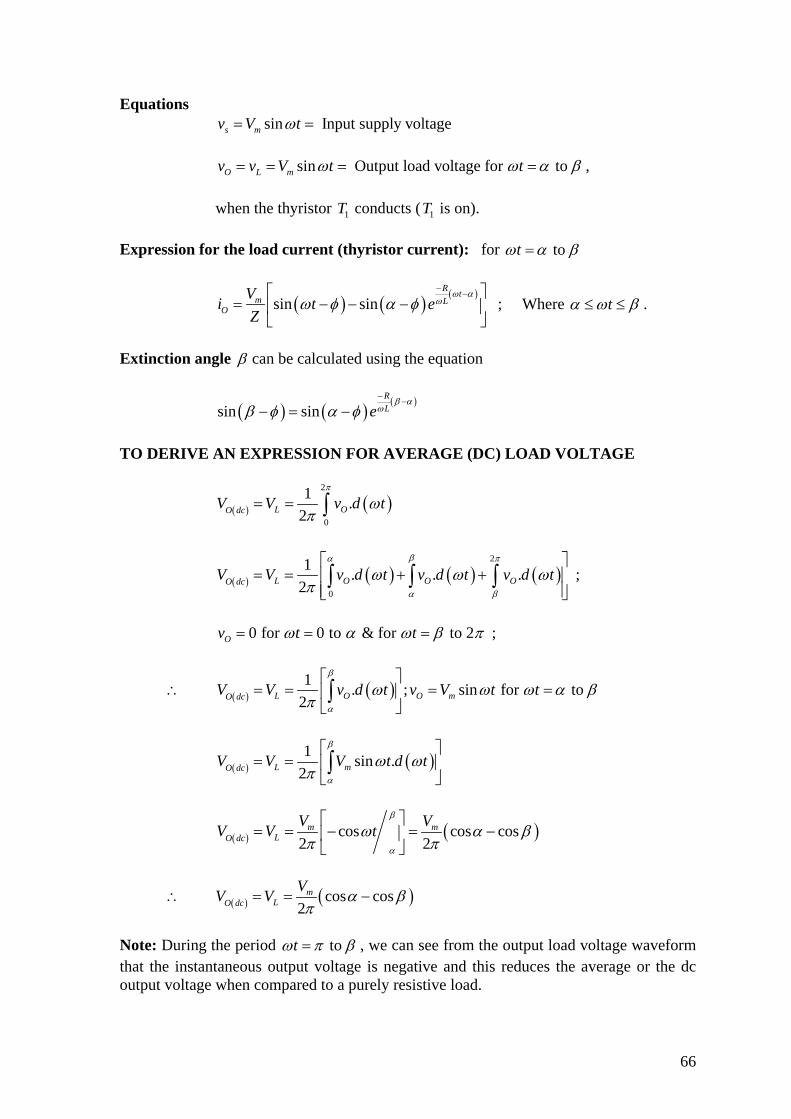
66
Equations sin Input supply voltages mv V tω= =
sin Output load voltage for to O L mv v V t tω ω α β= = = = ,
when the thyristor 1T conducts ( 1T is on).
Expression for the load current (thyristor current): for to tω α β=
( ) ( ) ( )sin sin
R tm LO
Vi t eZ
ω αωω φ α φ−
− = − − −
; Where tα ω β≤ ≤ .
Extinction angle β can be calculated using the equation
( ) ( ) ( )sin sin
RLe
β αωβ φ α φ−
−− = −
TO DERIVE AN EXPRESSION FOR AVERAGE (DC) LOAD VOLTAGE
( ) ( )2
0
1 .2L OO dcV V v d t
π
ωπ
= = ∫
( ) ( ) ( ) ( )2
0
1 . . .2L O O OO dcV V v d t v d t v d t
βα π
α β
ω ω ωπ
= = + +
∫ ∫ ∫ ;
0 for 0 to & for to 2Ov t tω α ω β π= = = ;
( ) ( )1 . ; sin for to 2L O O mO dcV V v d t v V t t
β
α
ω ω ω α βπ
∴ = = = =
∫
( ) ( )1 sin .2L mO dcV V V t d t
β
α
ω ωπ
= =
∫
( ) ( )cos cos cos2 2
m mLO dc
V VV V tβ
α
ω α βπ π
= = − = −
( ) ( )cos cos2
mLO dc
VV V α βπ
∴ = = −
Note: During the period to tω π β= , we can see from the output load voltage waveform that the instantaneous output voltage is negative and this reduces the average or the dc output voltage when compared to a purely resistive load.

67
Average DC Load Current
( ) ( )( ) ( )cos cos
2O dc m
O dc L AvgL L
V VI IR R
α βπ
= = = −
SINGLE PHASE HALF WAVE CONTROLLED RECTIFIER WITH RL LOAD AND FREE WHEELING DIODE
V0
i0T
R
L
Vs ~+
+
−
−
FWD
Fig. : Single Phase Half Wave Controlled Rectifier with RL Load and Free Wheeling Diode (FWD)
With a RL load it was observed that the average output voltage reduces. This disadvantage can be overcome by connecting a diode across the load as shown in figure. The diode is called as a Free Wheeling Diode (FWD). The waveforms are shown below.
2π
2π
3π
3π
π
π
α
α
α
α
0
0
0
0
Vs
iG
VO
ωt
ωt
ωt
ωt
Supply voltage
Load current
Load voltage
ωt=β
2π+α
Gate pulses
Vm
-Vm
α
π ββ 2π
iO

68
At tω π= , the source voltage Sv falls to zero and as Sv becomes negative, the free wheeling diode is forward biased. The stored energy in the inductance maintains the load current flow through R, L, and the FWD. Also, as soon as the FWD is forward biased, at tω π= , the SCR becomes reverse biased, the current through it becomes zero and the SCR turns off. During the period to tω π β= , the load current flows through FWD (free wheeling load current) and decreases exponentially towards zero at tω β= .
Also during this free wheeling time period the load is shorted by the conducting FWD and the load voltage is almost zero, if the forward voltage drop across the conducting FWD is neglected. Thus there is no negative region in the load voltage wave form. This improves the average output voltage.
The average output voltage [ ]1 cos2
mdc
VV απ
= + , which is the same as that of a
purely resistive load. The output voltage across the load appears similar to the output voltage of a purely resistive load.
The following points are to be noted. • If the inductance value is not very large, the energy stored in the
inductance is able to maintain the load current only upto tω β= , where2π β π< < , well before the next gate pulse and the load current tends to
become discontinuous.• During the conduction period to α π , the load current is carried by the
SCR and during the free wheeling period to π β , the load current iscarried by the free wheeling diode.
• The value of β depends on the value of R and L and the forwardresistance of the FWD. Generally 2π β π< < .
If the value of the inductance is very large, the load current does not decrease to zero during the free wheeling time interval and the load current waveform appears as shown in the figure.
2π 3ππα0 ωt
2π+α
t1
i0
SCR SCRFWD FWD
t3t2 t4
Fig. : Waveform of Load Current in Single Phase Half Wave Controlled Rectifier with a Large Inductance and FWD

69
During the periods 1 3, ,.....t t the SCR carries the load current and during the periods
2 4, ,.....t t the FWD carries the load current.
It is to be noted that • The load current becomes continuous and the load current does not fall to
zero for large value of load inductance.• The ripple in the load current waveform (the amount of variation in the
output load current) decreases.
SINGLE PHASE HALF WAVE CONTROLLED RECTIFIER WITH A GENERAL LOAD
A general load consists of R, L and a DC source ‘E’ in the load circuit
R
vS~+
− L
E+−
vO
iO
In the half wave controlled rectifier circuit shown in the figure, the load circuit consists of a dc source ‘E’ in addition to resistance and inductance. When the thyristor is in the cut-off state, the current in the circuit is zero and the cathode will be at a voltage equal to the dc voltage in the load circuit i.e. the cathode potential will be equal to ‘E’. The thyristor will be forward biased for anode supply voltage greater than the load dc voltage.
When the supply voltage is less than the dc voltage ‘E’ in the circuit the thyristor is reverse biased and hence the thyristor cannot conduct for supply voltage less than the load circuit dc voltage.
The value of tω at which the supply voltage increases and becomes equal to the load circuit dc voltage can be calculated by using the equation sinmV t Eω = . If we assume the value of tω is equal to γ then we can write sinmV Eγ = . Therefore γ is
calculated as 1sinm
EV
γ − =
.
For trigger angle α γ< , the thyristor conducts only from to tω γ β= .
For trigger angle α γ> , the thyristor conducts from to tω α β= .
The waveforms appear as shown in the figure
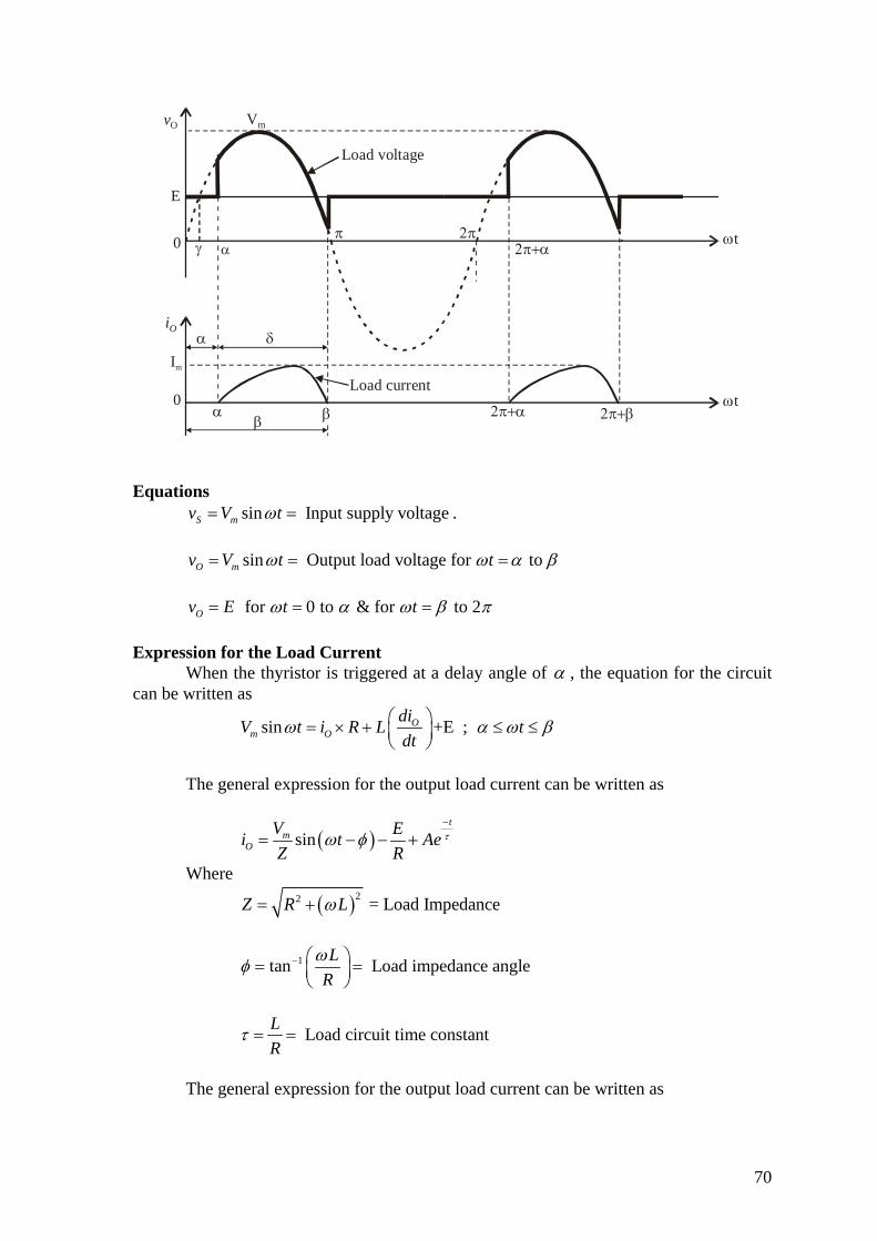
70
0
0
iO
ωt
ωt
Load current
E
vO
Load voltage
γ απ 2π
2π+α
Vm
Im
α β 2π+α 2π+β
α
β
δ
Equations sin Input supply voltageS mv V tω= = .
sin Output load voltage for to O mv V t tω ω α β= = =
for 0 to & for to 2Ov E t tω α ω β π= = =
Expression for the Load Current When the thyristor is triggered at a delay angle of α , the equation for the circuit
can be written as
sin +E ; Om O
diV t i R L tdt
ω α ω β = × + ≤ ≤
The general expression for the output load current can be written as
( )sint
mO
V Ei t AeZ R
τω φ−
= − − +
Where
( )22 = Load ImpedanceZ R Lω= +
1tan Load impedance angleLR
ωφ − = =
Load circuit time constantLR
τ = =
The general expression for the output load current can be written as

71
( )sinRtm L
OV Ei t AeZ R
ω φ−
= − − +
To find the value of the constant ‘A’ apply the initial condition at tω α= , load current 0Oi = . Equating the general expression for the load current to zero at tω α= , we get
( )0 sinR
m LO
V Ei AeZ R
αωα φ
−×
= = − − +
We obtain the value of constant ‘A’ as
( )sinR
m LVEA eR Z
αωα φ = − −
Substituting the value of the constant ‘A’ in the expression for the load current, we get the complete expression for the output load current as
( ) ( ) ( )sin sin
R tm m LO
V VE Ei t eZ R R Z
ω αωω φ α φ−
− = − − + − −
The Extinction angle β can be calculated from the final condition that the output current 0Oi = at tω β= . By using the above expression we get,
( ) ( ) ( )0 sin sin
Rm m L
OV VE Ei eZ R R Z
β αωβ φ α φ−
− = = − − + − −
To derive an expression for the average or dc load voltage
( ) ( )2
0
1 .2 OO dcV v d t
π
ωπ
= ∫
( ) ( ) ( ) ( )2
0
1 . . .2 O O OO dcV v d t v d t v d t
βα π
α β
ω ω ωπ
= + +
∫ ∫ ∫
sin Output load voltage for to O mv V t tω ω α β= = =
for 0 to & for to 2Ov E t tω α ω β π= = =
( ) ( ) ( )2
0
1 . sin .2 mO dcV E d t V t E d t
βα π
α β
ω ω ωπ
= + +
∫ ∫ ∫
( ) ( ) ( ) ( )2
0
1 cos2 mO dcV E t V t E t
πα β
βα
ω ω ωπ
= + − +

72
( ) ( ) ( ) ( )1 0 cos cos 22 mO dcV E V Eα β α π βπ
= − − − + −
( ) ( ) ( )cos cos 22 2
mO dc
V EV α β π β απ π
= − + − +
( ) ( ) ( )2cos cos
2 2m
O dcVV E
π β αα β
π π− −
= − +
Conduction angle of thyristor ( )δ β α= −
RMS Output Voltage can be calculated by using the expression
( ) ( )2
2
0
1 .2 OO RMSV v d t
π
ωπ
=
∫
DISADVANTAGES OF SINGLE PHASE HALF WAVE CONTROLLED RECTIFIERS Single phase half wave controlled rectifier gives
• Low dc output voltage.• Low dc output power and lower efficiency.• Higher ripple voltage & ripple current.• Higher ripple factor.• Low transformer utilization factor.• The input supply current waveform has a dc component which can result in dc
saturation of the transformer core.
Single phase half wave controlled rectifiers are rarely used in practice as they givelow dc output and low dc output power. They are only of theoretical interest.
The above disadvantages of a single phase half wave controlled rectifier can be over come by using a full wave controlled rectifier circuit. Most of the practical converter circuits use full wave controlled rectifiers.
SINGLE PHASE FULL WAVE CONTROLLED RECTIFIERS Single phase full wave controlled rectifier circuit combines two half wave
controlled rectifiers in one single circuit so as to provide two pulse output across the load. Both the half cycles of the input supply are utilized and converted into a uni-directional output current through the load so as to produce a two pulse output waveform. Hence a full wave controlled rectifier circuit is also referred to as a two pulse converter.
Single phase full wave controlled rectifiers are of various types • Single phase full wave controlled rectifier using a center tapped
transformer (two pulse converter with mid point configuration).• Single phase full wave bridge controlled rectifier
Half controlled bridge converter (semi converter). Fully controlled bridge converter (full converter).

73
SINGLE PHASE FULL WAVE CONTROLLED RECTIFIER USING A CENTER TAPPED TRANSFORMER
ACSupply
O
A
B
T1
T2
R L
vO
+
FWD
iO
iS
vS
Sv = Supply Voltage across the upper half of the transformer secondary winding
sinS AO mv v V tω= =
sinBO AO mv v V tω= − = − = supply voltage across the lower half of the transformer secondary winding.
This type of full wave controlled rectifier requires a center tapped transformer and two thyristors 1T and 2T . The input supply is fed through the mains supply transformer, the primary side of the transformer is connected to the ac line voltage which is available (normally the primary supply voltage is 230V RMS ac supply voltage at 50Hz supply frequency in India). The secondary side of the transformer has three lines and the center point of the transformer (center line) is used as the reference point to measure the input and output voltages.
The upper half of the secondary winding and the thyristor 1T along with the load act as a half wave controlled rectifier, the lower half of the secondary winding and the thyristor 2T with the common load act as the second half wave controlled rectifier so as to produce a full wave load voltage waveform.
There are two types of operations possible. Discontinuous load current operation, which occurs for a purely resistive
load or an RL load with low inductance value. Continuous load current operation which occurs for an RL type of load
with large load inductance.
Discontinuous Load Current Operation (for low value of load inductance) Generally the load current is discontinuous when the load is purely resistive or
when the RL load has a low value of inductance. During the positive half cycle of input supply, when the upper line of the
secondary winding is at a positive potential with respect to the center point ‘O’ the thyristor 1T is forward biased and it is triggered at a delay angle of α. The load current

74
flows through the thyristor 1T , through the load and through the upper part of the secondary winding, during the period to α β , when the thyristor 1T conducts.
The output voltage across the load follows the input supply voltage that appears across the upper part of the secondary winding from to tω α β= . The load current through the thyristor 1T decreases and drops to zero at tω β= , where β π> for RL type of load and the thyristor 1T naturally turns off at tω β= .
vOVm
0α
2π 3πα π β( )π+α ( )π+β
αβ
iO
ωt
ωt0
Fig.: Waveform for Discontinuous Load Current Operation without FWD
During the negative half cycle of the input supply the voltage at the supply line ‘A’ becomes negative whereas the voltage at line ‘B’ (at the lower side of the secondary winding) becomes positive with respect to the center point ‘O’. The thyristor 2T is forward biased during the negative half cycle and it is triggered at a delay angle of ( )π α+ . The current flows through the thyristor 2T , through the load, and through thelower part of the secondary winding when 2T conducts during the negative half cycle the load is connected to the lower half of the secondary winding when 2T conducts.
For purely resistive loads when L = 0, the extinction angle β π= . The load current falls to zero at tω β π= = , when the input supply voltage falls to zero at tω π= . The load current and the load voltage waveforms are in phase and there is no phase shift between the load voltage and the load current waveform in the case of a purely resistive load.
For low values of load inductance the load current would be discontinuous and the extinction angle β π> but ( )β π α< + .
For large values of load inductance the load current would be continuous and does not fall to zero. The thyristor 1T conducts from ( ) to α π α+ , until the next thyristor 2T
is triggered. When 2T is triggered at ( )tω π α= + , the thyristor 1T will be reverse biasedand hence 1T turns off.
75
TO DERIVE AN EXPRESSION FOR THE DC OUTPUT VOLTAGE OF A SINGLE PHASE FULL WAVE CONTROLLED RECTIFIER WITH RL LOAD (WITHOUT FREE WHEELING DIODE (FWD))
The average or dc output voltage of a full-wave controlled rectifier can be calculated by finding the average value of the output voltage waveform over one output
cycle (i.e., π radians) and note that the output pulse repetition time is 2T seconds where T
represents the input supply time period and 1Tf
= ; where f = input supply frequency.
Assuming the load inductance to be small so that β π> , ( )β π α< + we obtain discontinuous load current operation. The load current flows through 1T form
to tω α β= , where α is the trigger angle of thyristor 1T and β is the extinction angle where the load current through 1T falls to zero at tω β= . Therefore the average or dc output voltage can be obtained by using the expression
( ) ( )2 .2dc OO dc
t
V V v d tβ
ω α
ωπ =
= = ∫
( ) ( )1 .dc OO dct
V V v d tβ
ω α
ωπ =
= = ∫
( ) ( )1 sin .dc mO dcV V V t d tβ
α
ω ωπ
= =
∫
( ) cosmdcO dc
VV V tβ
α
ωπ
= = −
( ) ( )cos cosmdcO dc
VV V α βπ
= = −
Therefore ( ) ( )cos cosmO dc
VV α βπ
= − , for discontinuous load current operation,
( )π β π α< < + . When the load inductance is small and negligible that is 0L ≈ , the extinction
angle radiansβ π= . Hence the average or dc output voltage for resistive load is obtained as
( ) ( )cos cosmO dc
VV α ππ
= − ; cos 1π = −
( ) ( )( )cos 1mO dc
VV απ
= − −