a sub-pacurrent sensing front-end for transient induced
TRANSCRIPT

Symposia on VLSI Technology and Circuits
A Sub-pA Current Sensing Front-End for Transient Induced Molecular Spectroscopy
Da Ying, Ping-Wei Chen, Chi-Yang Tseng, Yu-Hwa Lo, and Drew A. Hall
University of California, San Diego, CA, USA

Symposia on VLSI Technology and Circuits
New Drug Discovery
• High-cost (>$2.6B/drug1) and failure rate from mid- to late-stage• Many diseases are highly linked to protein-ligand abnormality
Slide 1
Need a solution for accurate in-vitro study of protein-ligand interactions [1] Pharmaceutical Research and Manufacturers of America
[1]

Symposia on VLSI Technology and Circuits
Existing Methods for Protein-Ligand Detection
ü Binding kineticsû Immobilization of ligand
Slide 2
[1] J. Homola, Analytical and Bioanalytical Chemistry, 2003; [2] C. Fan, TRENDS in Biotechnology, 2005
[1]
Surface Plasmon Resonance
Labeling and immobilization significantly limit degree of freedom for binding
[2]
ü Solution phaseû Labelling of ligand
FRET

Symposia on VLSI Technology and Circuits
Transient Induced Molecular Spectroscopy (TIMES)
ü Label- and immobilization-free in-vitro protein-ligand detectionü Closer to physiological conditions and better signal integrity
Slide 3
Requires a sensitive AFE for charge sensingT. Zhang, Y. Lo, Scientific Reports, 2016
𝐼 =𝜕𝑄𝜕𝑡

Symposia on VLSI Technology and Circuits
µTIMES Specification
• Active area < 0.2 mm2/ch.• Partition across 4 references with 80dB SNDR each• WE/RE à pseudo-differential input
Slide 4
Parameter Application Circuit
Sensor size 8 channels 300µm×300µm M6
Resolution 0.1 µM sensitivity 100 fA
Cross-scale DR 0.1 µM – 10 mM range 100 fA – 1 µA
Bandwidth 5 cm/s flow rate 10 Hz
T. Zhang, Y. Lo, ACS Central Science, 2016

Symposia on VLSI Technology and Circuits
Existing Sub-pA Current AFEs
Slide 5
û Sensitive to aliasingû Input sampling à noise foldingû Charge injection to sensor
[H. Li, TBioCAS’16]
û Heavy digital backendû Large area, limited # of channels
[C. Hsu, ISSCC’18]
Aim to achieve 100fA sensitivity with small area/power

Symposia on VLSI Technology and Circuits
µTIMES à 1st-order current-mode ΔΣ + digital IIR (linear predictor)
Proposed µTIMES AFE Architecture
Slide 6
① 1-bit quantizer + digital IIR achieves quasi multi-bit quantization

Symposia on VLSI Technology and Circuits
Integrator only needs to process half of original pulse amplitude
Proposed µTIMES AFE Architecture
Slide 7
② Tri-level PWM avoids intensive hardware and relaxes filter linearity

Symposia on VLSI Technology and Circuits
Proposed µTIMES AFE Architecture
Slide 8
③ Multi-bit feedback effectively reduces 𝑓'
Lower 𝑓( relaxes speed requirement and improves anti-aliasing

Symposia on VLSI Technology and Circuits
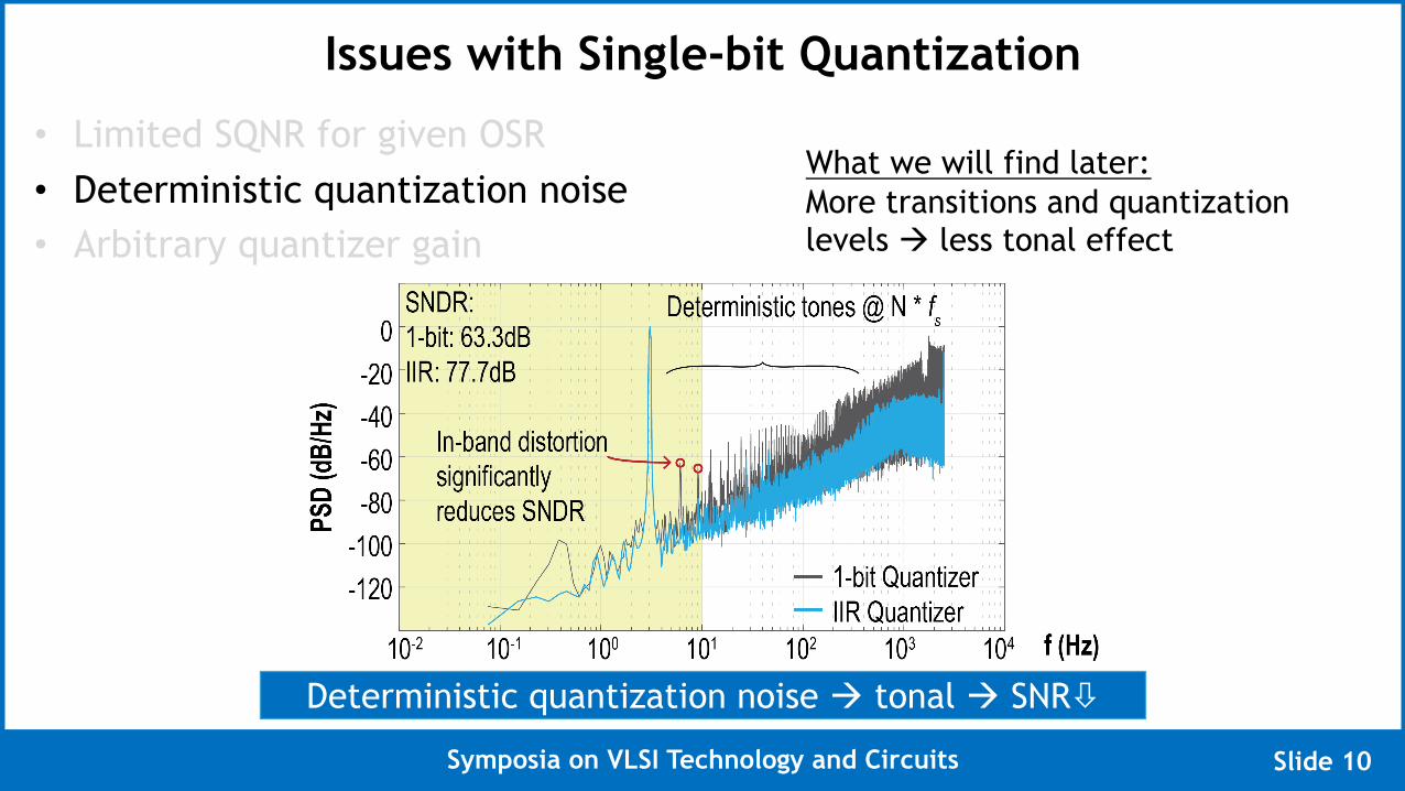
Issues with Single-bit Quantization
Slide 9
• Limited SQNR for given OSR• Deterministic quantization noise• Arbitrary quantizer gain
Limited SQNR à Large OSR à Power hungry & poor anti-aliasing
𝑂𝑆𝑅,-./𝑂𝑆𝑅0-./
∝ 23454670
𝑛 = Quantizer bits𝐿 = order
Symposia on VLSI Technology and Circuits
Issues with Single-bit Quantization
Slide 10
• Limited SQNR for given OSR• Deterministic quantization noise• Arbitrary quantizer gain
Deterministic quantization noise à tonal à SNRò
What we will find later:More transitions and quantization levels à less tonal effect

Symposia on VLSI Technology and Circuits
Issues with Single-bit Quantization
Slide 11
• Limited SQNR for given OSR• Deterministic quantization noise• Arbitrary quantizer gain
Arbitrary quantizer gain à deviate from linear model

Symposia on VLSI Technology and Circuits
Motivation: Linear Prediction in ΔΣ
Slide 12
𝑥 n + 1 = 𝑥 n +𝜕𝑥𝜕𝑡> ∆𝑇 = 𝑥 n + 𝑥 n − 𝑥[n − 1]
𝑫𝐨𝐮𝐭 n = 𝐷IJ/ n − 1 + 2×𝑄IJ/ n − 𝑄IJ/[n − 1]
à Multi-bit achieved with only a 4-bit adder, scaler, and two FFs
IIR filter àLMNO [P]QMNO[P]
= 43PRS
03PRS

Symposia on VLSI Technology and Circuits
Turning 1-bit Into Multi-bit
Slide 13
First-order observations:• Dout closely tracks input signal• More transitions à less tonal• Quantization step ∈ {∆, 3∆}• 𝑓(.Y,Z[\ and PSD?
Symposia on VLSI Technology and Circuits
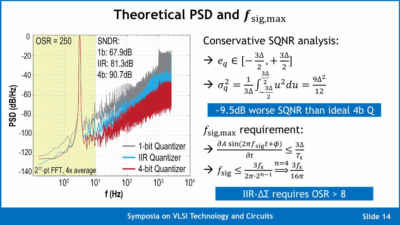
Theoretical PSD and 𝒇(.Y,Z[\
Slide 14
Conservative SQNR analysis:
à 𝑒_ ∈ [−`∆4, + `∆
4]
à 𝜎_4 =0`∆ ∫3c∆d
c∆d 𝑢4𝑑𝑢 = g∆d
04
𝑓(.Y,Z[\ requirement:
àhi (.,(4klmnop7q)
hp ≤ `∆tm
à 𝑓(.Y ≤`lm
4k>4uRS5vw `lm
0xk
~9.5dB worse SQNR than ideal 4b Q
IIR-ΔΣ requires OSR > 8

Symposia on VLSI Technology and Circuits
STF & NTF
Slide 15
𝑁𝑇𝐹(𝑧) = (2 − 𝑧30)(1 − 𝑧30)à 𝑆𝑇𝐹 𝑓 = 0
|4kl(2 − 𝑒3|4kl)(1 − 𝑒3|4kl)
• 1st-order shaping NTF• ~9dB larger out-of-band gain
Unity in-band STF & inherent anti-aliasing

Symposia on VLSI Technology and Circuits
IIR Quantizer Gain
Slide 16
• 𝑘 - smallest 𝜎~4 between quantizer input 𝑦 and output 𝑣– 𝑘 = 𝑣, 𝑦 / 𝑦, 𝑦 [1]
• Peak SNDR @ 0.8FS input level à define non-overloading range [0, 0.8FS]
𝑁𝑇𝐹� 𝑧 =2 − 𝑧301 − 𝑧30
1 + 𝑘 > 𝐿 𝑧
𝑁𝑇𝐹�(𝑧): NTF (𝑘 ≠ 1)𝐿 𝑧 : loop gain (𝑘 = 1)
𝑘 shows IIR quantizer can be statistically approximated as a multi-bit quantizer[1] S. Pavan, R. Schreier, G. Temes, ‘Understanding delta-sigma data converters’, John Wiley & Sons, 2017
Symposia on VLSI Technology and Circuits
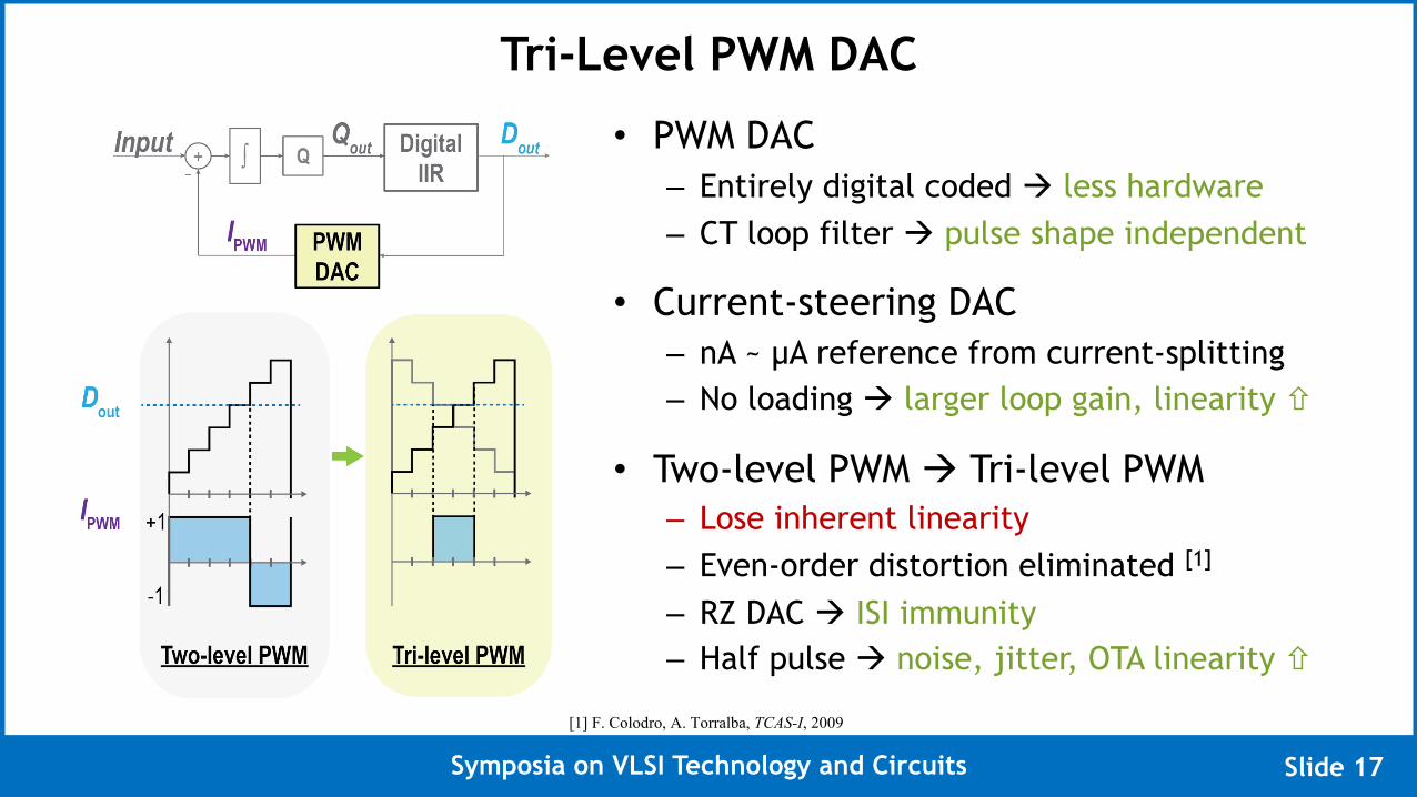
Tri-Level PWM DAC
Slide 17
• PWM DAC– Entirely digital coded à less hardware– CT loop filter à pulse shape independent
• Current-steering DAC– nA ~ µA reference from current-splitting– No loading à larger loop gain, linearity ñ
• Two-level PWM à Tri-level PWM– Lose inherent linearity– Even-order distortion eliminated [1]
– RZ DAC à ISI immunity– Half pulse à noise, jitter, OTA linearity ñ
[1] F. Colodro, A. Torralba, TCAS-I, 2009
Symposia on VLSI Technology and Circuits
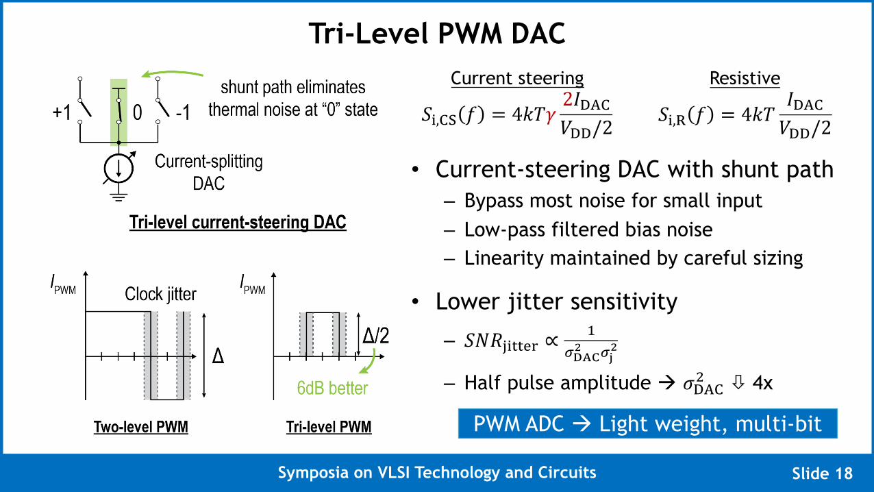
Tri-Level PWM DAC
Slide 18
• Current-steering DAC with shunt path– Bypass most noise for small input– Low-pass filtered bias noise– Linearity maintained by careful sizing
• Lower jitter sensitivity
– 𝑆𝑁𝑅�.//�� ∝0
����d ��
d
– Half pulse amplitude à 𝜎���4 ò 4x
Current steering
𝑆.,�� 𝑓 = 4𝑘𝑇𝛾2𝐼���𝑉��/2
Resistive
𝑆.,� 𝑓 = 4𝑘𝑇𝐼���𝑉��/2
PWM ADC à Light weight, multi-bit

Symposia on VLSI Technology and Circuits
Current-Splitting DAC
Slide 19
C. Enz, E. Vittoz, ISCAS, 1996
Symposia on VLSI Technology and Circuits
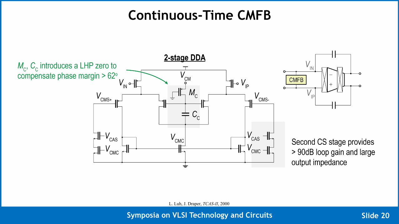
Continuous-Time CMFB
Slide 20
L. Luh, J. Draper, TCAS-II, 2000

Symposia on VLSI Technology and Circuits
Chip Micrograph
Slide 21
DAC16%
Integrator55%
Bias22%
Total power: 50.3µW/ch* Comparator and digital logic consumes negligible power
28µW
11µW 8µW3.5µ
W
CMFB7%
Symposia on VLSI Technology and Circuits
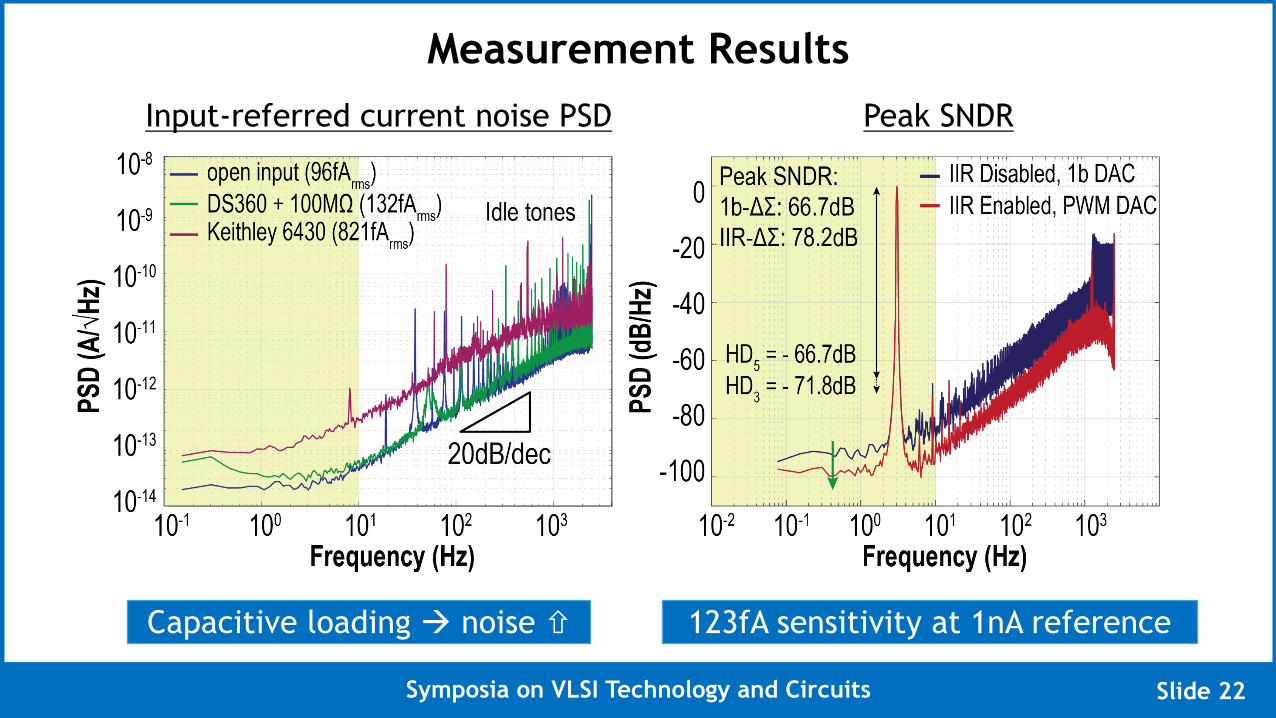
Measurement Results
Slide 22
Input-referred current noise PSD Peak SNDR
Capacitive loading à noise ñ 123fA sensitivity at 1nA reference

Symposia on VLSI Technology and Circuits
Measurement Results
Slide 23
SNDR vs. input amplitude
78.2dB fixed-scale dynamic range

Symposia on VLSI Technology and Circuits
Measurement Results
Slide 24
DC input sweep
139dB cross-scale dynamic range

Symposia on VLSI Technology and Circuits
TIMES In-vitro Measurement Setup
Slide 25
To inlets
FPGA power
FPGA USB
Power supply
µTIMES & microfluidic
PDMS cross-section
ENIG sensors
3 mm

Symposia on VLSI Technology and Circuits
In-vitro Protein-Ligand Measurement
Slide 26
Characteristic shape due to unique dipole moment and charge locality

Symposia on VLSI Technology and Circuits
Performance Summary
Slide 27
Stanaćević TBCAS’07
Li TBCAS’16
Sim TBCAS’17
Hsu ISSCC’18
Nazari TBCAS’13
This Work
AFE Architecture Inc. ΔΣ Inc. ΔΣ ΔΣ Hourglass ΔΣ
CC + SS ADC IIR-ΔΣ
Process [µm] 0.5 0.5 0.35 0.18 0.35 0.18 Max Input [µA] 1 16 2.8 10 0.35 1.1 Resolution [fA]
@ BW [Hz] 100
@ 0.1 100 @ 1
100,000 @ 10
100 @ 1.8
24,000 @ 100
123 @ 10
Conversion Time @ Min. Input [ms] 8,388 1,000 4 400 10 100
Input-referred Noise [fA/√Hz] - - 6,960 58.9 1,850 30.3
Fixed-/cross- scale DR [dB]
40* / 140
54.0* / 164 77.5 160 60.7 /
95 78.2 / 139
On-chip Sensors? NO NO NO NO YES YES Num. of Channels 16 50 1 1 192 8
Area/ch. [mm2] 0.25* 0.157 0.5 0.2† 0.04 0.11 Power/ch. [µW] 3.4‡ 241 16.8 295 188 50.3
* estimated from figures; † not including synthesized digital area and DEM; ‡ off-chip bias

Symposia on VLSI Technology and Circuits
Performance Summary
Slide 28
Stanaćević TBCAS’07
Li TBCAS’16
Sim TBCAS’17
Hsu ISSCC’18
Nazari TBCAS’13
This Work
AFE Architecture Inc. ΔΣ Inc. ΔΣ ΔΣ Hourglass ΔΣ
CC + SS ADC IIR-ΔΣ
Process [µm] 0.5 0.5 0.35 0.18 0.35 0.18 Max Input [µA] 1 16 2.8 10 0.35 1.1 Resolution [fA]
@ BW [Hz] 100
@ 0.1 100 @ 1
100,000 @ 10
100 @ 1.8
24,000 @ 100
123 @ 10
Conversion Time @ Min. Input [ms] 8,388 1,000 4 400 10 100
Input-referred Noise [fA/√Hz] - - 6,960 58.9 1,850 30.3
Fixed-/cross- scale DR [dB]
40* / 140
54.0* / 164 77.5 160 60.7 /
95 78.2 / 139
On-chip Sensors? NO NO NO NO YES YES Num. of Channels 16 50 1 1 192 8
Area/ch. [mm2] 0.25* 0.157 0.5 0.2† 0.04 0.11 Power/ch. [µW] 3.4‡ 241 16.8 295 188 50.3
* estimated from figures; † not including synthesized digital area and DEM; ‡ off-chip bias

Symposia on VLSI Technology and Circuits
Performance Summary
Slide 29
Stanaćević TBCAS’07
Li TBCAS’16
Sim TBCAS’17
Hsu ISSCC’18
Nazari TBCAS’13
This Work
AFE Architecture Inc. ΔΣ Inc. ΔΣ ΔΣ Hourglass ΔΣ
CC + SS ADC IIR-ΔΣ
Process [µm] 0.5 0.5 0.35 0.18 0.35 0.18 Max Input [µA] 1 16 2.8 10 0.35 1.1 Resolution [fA]
@ BW [Hz] 100
@ 0.1 100 @ 1
100,000 @ 10
100 @ 1.8
24,000 @ 100
123 @ 10
Conversion Time @ Min. Input [ms] 8,388 1,000 4 400 10 100
Input-referred Noise [fA/√Hz] - - 6,960 58.9 1,850 30.3
Fixed-/cross- scale DR [dB]
40* / 140
54.0* / 164 77.5 160 60.7 /
95 78.2 / 139
On-chip Sensors? NO NO NO NO YES YES Num. of Channels 16 50 1 1 192 8
Area/ch. [mm2] 0.25* 0.157 0.5 0.2† 0.04 0.11 Power/ch. [µW] 3.4‡ 241 16.8 295 188 50.3
* estimated from figures; † not including synthesized digital area and DEM; ‡ off-chip bias

Symposia on VLSI Technology and Circuits
Conclusion
Slide 30
Motivation:• A compact, energy-efficient, high-sensitivity AFE for TIMES biosensing
Techniques:• Linear prediction in 1st-order CT-ΔΣ achieved by digital IIR filter• Relaxed hardware complexity with tri-level PWM DAC
Results:• Low-noise (30.3fA/√Hz)• High sensitivity (123fA)• Large dynamic range (78.2dB/139dB)• Small area (0.11mm2) and low power (50.3µW) per channel

Symposia on VLSI Technology and Circuits
Acknowledgement
Slide 31
• This work was supported in part by the National Science Foundation under Grant ECCS-1610516.
Thank you for your attention!