sensing photo-induced surface charges on organic photo...
TRANSCRIPT

Sensing photo-induced surface charges on OrganicPhoto-Voltaic materials using Atomic Force Microscopy
RICCARDO BORGANI [email protected]
SK200X Degree Project in Applied Physics, Second CycleDepartment of Applied Physics, Nanostructure Physics
Supervisor: Daniel ForchheimerExaminer: David Haviland
TRITA-FYS 2014:03 ISSN 0280-316X ISRN KTH/FYS/–14:03–SE

ii

iii
Abstract
A new method for sensing photo-induced surface charges on organic photo-voltaicmaterials is proposed and analyzed. The method relies on measuring photo-inducedelectrostatic forces between the sample surface and the probe of an atomic force micro-scope (AFM) by means of a non-linear technique called intermodulation spectroscopy.A computer simulation and a proof of concept of the method are presented, as well asa detailed description of the sample preparation. Finally, the main challenges for thismethod, namely sample degradation and light illumination set-ups, are discussed andfurther improvements are proposed.
Sammanfattning
En ny metod för att detektera fotoinducerade ytladdningar på organiska fotovol-taiska material har föreslagits och analyserats. Metoden bygger på att mäta fotoinduce-rade elektrostatiska krafter mellan en provyta och spetsen på ett atomkraftsmikroskop(AFM) med hjälp av en icke-linjär teknik som kallas intermodulation spektroskopi. Endatorsimulering och ett bevis på konceptet av metoden presenteras, såväl som en de-taljerad beskrivning av tillverkningen av proverna. De största utmaningarna för dennametod, vilka var nedbrytning av den organiska materialen och illuminationsuppställ-ningen, diskuteras varpå ytterligare förbättringar föreslås.

Contents
Contents iv
1 Introduction 11.1 Organic photovoltaic materials . . . . . . . . . . . . . . . . . . . . . . . . . 11.2 Atomic Force Microscopy (AFM) . . . . . . . . . . . . . . . . . . . . . . . . 21.3 Measuring force with AFM: Intermodulation AFM . . . . . . . . . . . . . . 31.4 Measuring surface charge with AFM: Kelvin Probe Force Microscopy (KPFM) 41.5 Measuring current with AFM: Conductive AFM . . . . . . . . . . . . . . . 4
2 Sensing time-dependent electrostatic forces with ImAFM 62.1 The method . . . . . . . . . . . . . . . . . . . . . . . . . . . . . . . . . . . . 62.2 Computer simulation . . . . . . . . . . . . . . . . . . . . . . . . . . . . . . . 82.3 Proof of concept with EFM . . . . . . . . . . . . . . . . . . . . . . . . . . . 92.4 Measurement on an organic solar cell . . . . . . . . . . . . . . . . . . . . . . 10
3 Sample preparation and characterization 123.1 Cleaning of the substrate . . . . . . . . . . . . . . . . . . . . . . . . . . . . 123.2 Spin-coating . . . . . . . . . . . . . . . . . . . . . . . . . . . . . . . . . . . . 133.3 AFM images and force reconstruction . . . . . . . . . . . . . . . . . . . . . 133.4 I-V characteristic measurement . . . . . . . . . . . . . . . . . . . . . . . . . 17
4 Experimental set-up 214.1 Bottom-up illumination . . . . . . . . . . . . . . . . . . . . . . . . . . . . . 214.2 Total internal reflection illumination . . . . . . . . . . . . . . . . . . . . . . 22
Calculation of the emission angle . . . . . . . . . . . . . . . . . . . . . . . . 224.3 Intermodulation lock-in analyzer (ImLA) . . . . . . . . . . . . . . . . . . . 23
5 Challenges 245.1 Effect of direct light on the cantilever . . . . . . . . . . . . . . . . . . . . . 24
Measurement and analysis . . . . . . . . . . . . . . . . . . . . . . . . . . . . 245.2 Degradation of the sample . . . . . . . . . . . . . . . . . . . . . . . . . . . . 26
6 Conclusions 27
Bibliography 29
iv
Chapter 1
Introduction
1.1 Organic photovoltaic materials
The conversion of sunlight into electrical energy, photovoltaics, represents a very importanttechnique in all those applications that require an energy source which is clean and sustain-able, such as providing power to national energy grids, portable storage for mobile devices,or in those situation where sun is the only abundant energy source available, such as forsatellites and space missions.
Although the vast majority of materials used nowadays for photovoltaics are inorganic,in the past four decades big effort has been put into developing organic solar cells[1].
Organic solar cells commonly rely on the usage of polymers with semiconducting proper-ties. The first big difference between organic and inorganic semiconductors lies in the muchlower charge-carrier mobility in organic materials. On the other hand, organic materialsgenerally present much higher absorptions which allow for the design of very thin devices,thus partly overcoming the poor mobility limitation[1].
Another difference between inorganic and organic materials for photovoltaics is the op-tical band gap, which for the latter is of about 2 eV. This puts a strong limitation on theabsorbable solar spectrum with respect to materials such as silicon with an optical bandgap of about 1 eV.
Despite these limitations, the possibility of synthesizing polymers in countless differentvariations, the perspective of low-cost and large-scale production, and the integrability oforganic solar cells into many different products, are pushing the research in this field inboth academia and industry[1].
To bring organic solar cells from research facilities into practical application, two im-portant specifications need to be addressed: lifetime of the photovoltaic device and powerconversion efficiency. While the former can be substantially improved with encapsulationtechniques which limit the interaction of the active material with oxygen and water, thelatter requires a deeper understanding and control of the device morphology and chargedynamics at the nanoscale[1, 2].
Once a photon is absorbed in the active material, an exciton is formed and it mustdiffuse to a site where it can dissociate into two free charges which can be transported tothe electrodes and extracted. Both the exciton diffusion and charge transport processes arestrongly dependent on the morphology, which therefore has a strong impact on the overallperformance of the device.
To ensure an efficient dissociation of excitons, they must be generated within one excitondiffusion length from the donor-acceptor interface in the active layer. In this respect, one
1
CHAPTER 1. INTRODUCTION 2
Figure 1.1
of the most promising types of organic solar cells are bulk heterojunction devices whichrequire stable and nanometer-sized donor and acceptor domains[2].
On the other hand, too intimate mixing of the different polymers can lead to too smallmean free path for the charge-carriers which therefore cannot reach the electrodes beforerecombining. The molecular structure, nanoscale morphology and final device propertiesare thus closely related to each other[1].
Our work has the aim to develop a new method to image the distribution of chargecarriers at the device surface with nanometer resolution, as well as sense the dynamics ofthe generation and recombination of the charge carriers. We hope this would lead to adeeper understanding of the physics involved in the process of conversion of sunlight intoelectrical energy and the ability to design better performing devices.
1.2 Atomic Force Microscopy (AFM)
Since its invention in 1986 by Binnig and Quate[3], the Atomic Force Microscope (AFM) hasproven to be an effective and versatile tool to image[4], to investigate mechanical, electricaland magnetic properties of materials[5], and to perform manipulation of structures[6] at thenanometer scale.
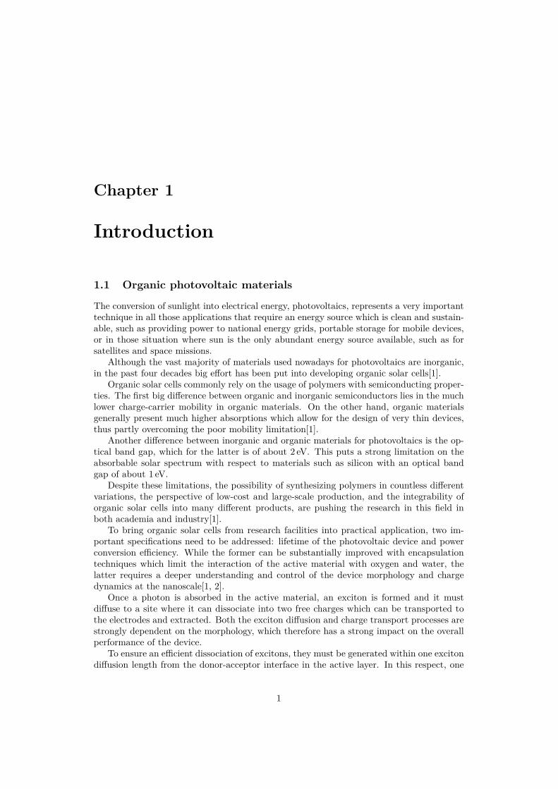
Figure 1.1 shows a simplified scheme of the atomic force microscope.A key component of the AFM system is the force transducer which is a micrometric
cantilever, usually made of heavily doped silicon, clamped at one end and free to oscillateat the other. The deflection of the cantilever, and thus its dynamics, can be detected in realtime by means of an optical lever system. Typical dimensions for a rectangular cantileverare 100− 200µm length, 20− 40µm width and 2− 8µm thickness.
A small tip, attached at the free end of the cantilever, interacts with the sample surfacethrough different types of forces, e.g. mechanical, electrostatic, magnetic, or chemical forcesdepending on the material of the surface and the AFM operation mode. Typical dimensionsfor an AFM tip are 10− 20µm height and 8− 35 nm radius at the tip apex.
The position of the tip relative to the sample can be controlled in three directionsby a piezo-electric positioning system. An additional piezo shaker can be used to exciteoscillations of the cantilever. There are several standard modes of operating the AFM, wewill discuss the two most common ones.
CHAPTER 1. INTRODUCTION 3
In quasi-static AFM, the tip is slowly brought in contact with the surface until the ver-tical deflection signal reaches a pre-defined set-point. The tip then scans over the samplewhile a feedback system acts on the z-piezo to maintain the cantilever vertical deflectionconstant at the set-point. A representation of the z-piezo extension as a function of theposition of the tip over the sample is usually referred to as height image and gives quantita-tive information about the topography of the surface. During the scan the tip-surface forceis kept in the repulsive (contact) regime and the image is recorded at a roughly constantinteraction force, depending on the chosen set-point. The feedback error signal (verticaldeflection error) is also imaged as it provides additional qualitative information about thesurface.
In dynamic AFM, the cantilever is made to oscillate close to its resonance frequency(typically 300− 1000 kHz) by shaking its base with a piezo. Typical oscillation amplitudesare of the order of 100 nm. The amplitude of oscillation is monitored and the tip engages thesurface when the oscillation amplitude drops below a predefined set-point. During the scan,the feedback system acts on the z-piezo to maintain the cantilever oscillation amplitudeconstant at the set-point. As in quasi-static AFM, the height image provides quantitativeinformation about the topography of the surface. Moreover the feedback error signal (oramplitude error) and the phase shift between the cantilever oscillation and the piezo shakerdrive are usually imaged to provide additional qualitative information about the surface.
While quasi-static AFM allows for a more straightforward interpretation of the heightimage, with dynamic AFM both tip and sample degradation are minimized due to lowercontact and lateral forces between the tip and the surface[7].
1.3 Measuring force with AFM: Intermodulation AFM
Intermodulation atomic force microscopy[8] (ImAFM) is a multi-frequency measurementmethod of dynamic AFM. The cantilever oscillation is driven with a signal consisting oftwo pure tones close to resonance instead of only one, and the relative amplitudes andphases at the two drive frequencies f1 and f2 are usually adjusted so that the free cantileveroscillation response amplitudes at the same two frequencies are equal to each other: in thisway the free oscillation forms a beat with 50 % modulation depth, where the carrier signalhas frequency f1+f2
2 and the modulating signal has frequency f2−f12 . Figure 1.2 shows the
cantilever deflection signal in the time and in the frequency domains.When the cantilever experiences a non-linear force, e.g. when subject to tip-surface
forces, the phenomenon of intermodulation distortion appears: the response oscillationcontains signals not only at the two drive frequencies f1 and f2, but also at frequencies givenby integer linear combinations of the two: n1f1+n2f2, n1,2 = 0, ±1, ±2, . . ., where |n1|+|n2|is called order of intermodulation. The relative amplitudes and phases of the response atthose frequencies carry information about the non-linear force that generated them.
If the two drive frequencies are chosen to be closely separated and centered around thecantilever mechanical resonance, the response will contain several odd order intermodu-lation products around resonance. This allows for a sensitive measurement of the spec-tral components of the non-linear force and thus provides an effective method for forcereconstruction[9].
Many multi-frequency AFM techniques have been developed[9, 10, 11, 12, 23], wherethe measurement of multiple frequency components of the cantilever response is used toreconstruct the tip-surface force. The advantage of the intermodulation technique is that,thanks to its drive scheme, a large number of the frequency components of the response areconcentrated around the mechanical resonance of the cantilever and it is therefore possible

CHAPTER 1. INTRODUCTION 4
(a) (b)
Figure 1.2: Cantilever deflection signal during a ImAFM experiment in the time and in thefrequency domain: (a) far from the surface, response at the two drive frequencies only; (b)engaged to the surface, intermodulation products arise on both sides of the drive frequencies.
to measure them with a very high signal to noise ratio. This allows for a very sensitivemeasurement, being limited by the thermal noise force only[9].
Examples of ImAFM force reconstructions are shown in section 3.3.
1.4 Measuring surface charge with AFM: Kelvin Probe ForceMicroscopy (KPFM)
The ability of the AFM cantilever to act as a sensitive force transducer for different typesof tip-surface forces allows for imaging techniques that map different properties of thesample such the electrostatic surface potential. Different techniques have been developedbut Kelvin Probe Force Microscopy (KPFM) is one of the most widely used and is able toprovide quantitative information on local changes in the surface potential and tip-surfacecapacitance gradient for both inorganic and organic materials[13, 14].
Although various KPFM modes exist, depending on the type of modulation used in themeasurement and whether the probe is in contact with the surface or just oscillating aboveit, the principle of operation remains the same: when an AC voltage potential is applied tothe AFM tip, oscillating electrostatic forces arise between the tip and the sample. Measuringthe amplitude of these forces with a lock-in amplifier allows for the reconstruction of thesurface potential of the sample[13]. Examples of KPFM images are shown in section 3.3.
1.5 Measuring current with AFM: Conductive AFM
The usage of a conductive probe (e.g. platinum iridium coated cantilevers and tips) allowsfor the measurement of current-voltage (I-V) characteristics and local changes in resistance(or conductance) of materials at the nanometer scale.
Typically a conductive AFM (CAFM), or conducting probe AFM (CPAFM), experi-ment consists in acquiring a quasi-static AFM image with a constant DC potential appliedbetween the probe and the sample[15]. A current amplifier is used to measure the electriccurrent passing through the probe while scanning the surface to create a current image thatgives quantitative information about the local variations in resistance of the sample.
CHAPTER 1. INTRODUCTION 5
A critical issue in this technique is the wearing of the tip and in particular the damage ofthe conductive coating of the probe due to the strong and constant lateral tip-surface forcestypical of quasi-static AFM. For this reason in our experiments the Bruker Co. proprietarysolution PeakForce™ TUNA has been used. With this technique the z-piezo is modulatedat a frequency of about 1 kHz and a complete fast force curve is measured at every pixelof the image. The peak interaction force of each curve is used as the imaging feedbacksignal. The average current over one full taping cycle is also measured and used to imagethe conductive properties of the sample. The lower interaction and lateral forces provide alonger wearing time of the tip coating.
Alternatively, while the probe is in contact with the surface at a fixed location, thevoltage bias between the tip and the sample can be changed linearly to measure current asa function of the applied voltage (I-V characteristic).
Examples of PeakForce™ TUNA images and I-V characteristics are shown in section 3.3.
Chapter 2
Sensing time-dependent electrostaticforces with ImAFM
2.1 The method
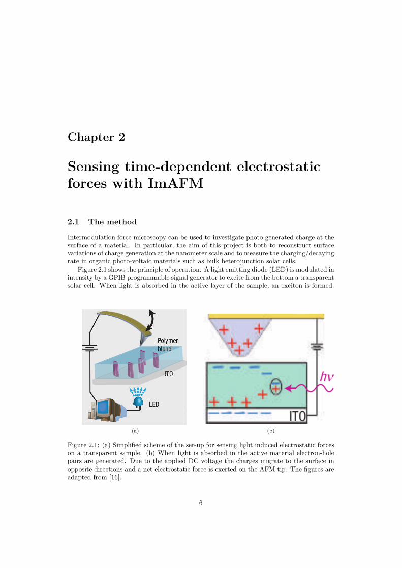
Intermodulation force microscopy can be used to investigate photo-generated charge at thesurface of a material. In particular, the aim of this project is both to reconstruct surfacevariations of charge generation at the nanometer scale and to measure the charging/decayingrate in organic photo-voltaic materials such as bulk heterojunction solar cells.
Figure 2.1 shows the principle of operation. A light emitting diode (LED) is modulated inintensity by a GPIB programmable signal generator to excite from the bottom a transparentsolar cell. When light is absorbed in the active layer of the sample, an exciton is formed.
(a) (b)
Figure 2.1: (a) Simplified scheme of the set-up for sensing light induced electrostatic forceson a transparent sample. (b) When light is absorbed in the active material electron-holepairs are generated. Due to the applied DC voltage the charges migrate to the surface inopposite directions and a net electrostatic force is exerted on the AFM tip. The figures areadapted from [16].
6

CHAPTER 2. SENSING TIME-DEPENDENT ELECTROSTATIC FORCES WITHIMAFM 7
(a) (b) (c)
Figure 2.2: Conceptual illustration of: (a) light intensity and induced charge surface densityas a function of time; (b) charge surface density frequency spectrum; (c) intermodulationproducts arising around the cantilever drive frequency due to a non-linear force.
The exciton diffuses to the interface between two polymers with different hole and electronmobility and separates in two free charges. If a DC potential is applied to the sample, thetwo charges drift in opposite directions to the top and the bottom surfaces. This chargeseparation creates a net electrostatic force on the AFM tip modifying its dynamics. Byanalyzing the cantilever deflection signal in the frequency domain it is then possible toreconstruct the electrostatic force as a function of position of the tip above the surface.
If the LED emission intensity is modulated in time at low frequency, the charge densityat the surface of the sample will also be a function of time and therefore produce a timedependent electrostatic force on the AFM tip. If the electrostatic force is non-linear, inter-modulation products will arise around the cantilever drive frequency. The analysis of theintermodulation spectrum will then allow for a reconstruction of the force as a function oftime by assuming a model for the time behavior of the photo-generated charge.
To illustrate the concept, let’s assume that a train of very short and intense light pulseswith period T = 1 s would induce a charge surface density s (t) of the form of an exponentialdecay with time constant τ = 0.2 s, Figure 2.2.a:
s (t) = exp[− (t− nT )
τ
], n = 0,±1,±2, . . .
The discrete Fourier transform s (f) of such a signal (sampled with 1024 samples perperiod and integrated over 16 periods) is shown in Figure 2.2.b. The amplitudes and phasesat frequencies multiple of the inverse of the repetition period fL = 1
T = 1 Hz are given bythe Fourier transform of the base signal exp
[−tτ
]:
s (nfL) =[
τ
1 + i2πfτ
]f=nfL
If the cantilever is oscillating at a much higher frequency, say fDRIVE = 200 Hz, and theforce on the cantilever due to s (t) is non-linear, by acquiring the frequency spectrum ofthe cantilever deflection signal d (f) we would observe several intermodulation products atfrequencies fDRIVE ± nfL, n = ±1,±2, . . . (Figure 2.2.c).
In general, the amplitudes and phases of the intermodulation products will depend on theexpression of the non-linear force. For the sake of simplicity let’s assume that the effect of thenon-linearity is only to up-convert the low frequency spectrum s (f) around the cantileverdrive frequency, up to a scaling factor. With this assumption, the measurement of the
CHAPTER 2. SENSING TIME-DEPENDENT ELECTROSTATIC FORCES WITHIMAFM 8
relative amplitudes of the intermodulation products makes possible to perform a non-linearcurve fitting to extract the parameter τ from the measured spectrum. We demonstrated thevalidity of this approach by performing a computer simulation and by using electrostaticforce microscopy.
2.2 Computer simulation
The source code of the simulation has been written in Python, and the differential equationgoverning the cantilever dynamics has been numerically integrated using odeint which isa wrapper for lsoda, the numerical integrator used in SciPy.
A simple one dimensional damped harmonic oscillator model has been assumed for thecantilever dynamics:
z (t) = −ω20 [z (t)− h]− ω0
Qz (t) + ω2
0kFTOT (t, z)
where z is the tip-surface distance, or tip height, h is the cantilever base height, ω0,Q, and k are the cantilever resonance frequency, quality factor and stiffness, respectively,and FTOT is the total force acting on the cantilever.
In our simulation, the total force is assumed to be the sum of two contributions: thedrive force FDRIVE consisting of a pure sine wave with frequency ω0; and the electrostaticforce between the tip and the sample FEL. FEL is modeled assuming a simple Coulombforce model:
FEL (t, z) = − 14πε0
V (t)2
z2
where V 2 is the tip-sample voltage potential difference and ε0 is the vacuum permittiv-ity. This approximation is valid in the limit of tip not in contact with the surface (onlyelectrostatic forces) and of a tip-surface distance z large compared to the tip radius[17].
In order to simulate the effect of the photo-generated charge on the cantilever when thelight is pulsed at a frequency fL, the electrostatic potential has been modeled as:
V (t) = e−t−nTτ , n = 0, ±1, ±2, . . .
where T = 1/fL is the repetition period of the light pulses and τ is a characteristic decaytime of the photo-generated charges. The square absolute value of the Fourier transform ofsuch a signal is: ∣∣∣V (ω)
∣∣∣2 = τ2
1 + ω2τ2 δ
(ω − n2π
T
)(2.1)
In our simulation we chose fDRIVE = 256fL, a quality factor Q = 100, a spring con-stant k = 100 N/m and a sampling frequency fS = 1024fL. Once the cantilever motion z (t)has been numerically solved for a particular value of τ , its fast Fourier transform z (f) iscomputed. As shown in Figure 2.3.a, due to the non-linear force FEL several intermodula-tion products appear around resonance with spacing fL. The force acting on the cantileveris obtained by diving the cantilever motion by the linear transfer function of the harmonicoscillator[9]. By shifting the intermodulation products on the right hand side of the drivesignal to the left by fDRIVE (Figure 2.3.b), it is possible to perform a nonlinear curve fitwith equation 2.1 to obtain the value of τ . In our analysis the fit has been performed over10 intermodulation products.

CHAPTER 2. SENSING TIME-DEPENDENT ELECTROSTATIC FORCES WITHIMAFM 9
(a) (b) (c)
Figure 2.3: Computer simulation of the cantilever response to an exponential decayingelectrostatic force: (a) intermodulation products arise around the drive frequency due tothe non-linear electrostatic force, the green dots represent the amplitudes used in the fit;(b) non-linear fit for τ = T
100 ; (c) non-linear curve fit result for different simulated valuesof τ (blue dots), the blue line is the curve y = τ , the red dots represent the fit absoluterelative error.
Figure 2.3.c shows the fit results for different simulations where the value of τ has beenchanged in the range τ = T
1000 ÷ 10T . We notice that the fitting algorithm is able to find agood estimation of τ if it is larger than ≈ 5T · 10−3, which corresponds to τ > 1
fDRIVE.
A hand-waving argument for the above limitation is that, in order to properly reconstructthe force from the modulation of the cantilever motion, the force must vary slowly on thetime scale of the cantilever motion itself.
Another limit is visible in Figure 2.3.c: the fit error becomes large also when τ is largewith respect to the pulse repetition period T . When the time constant is large compared tothe period, the force amplitude is almost constant during the integration time (equal to T )and thus the cantilever motion is barely affected by it.
In conclusion, these two constrains show that this method is able to provide a goodestimation for the time constant τ when:
1fDRIVE
< τ <1fL
(2.2)
2.3 Proof of concept with EFM
To demonstrate the practical feasibility of this method, we used electrostatic force mi-croscopy (EFM) to induce electrostatic forces between the tip and the sample[18]. In EFMthe probe and a conducting sample form a capacitor structure and changes in the potentialacross this capacitor induce changes in the force and the force gradient in a way similar toour previous computer simulation.
In our experiment, the sample was a gold layer grown on a silicon wafer connectedto ground. A programmed exponential decaying voltage was applied directly to the tip bymeans of a GPIB programmable arbitrary waveform generator. The probe was an Antimonydoped Si probe and was calibrated with the thermal noise technique[19] (f0 = 423.72 kHz,Q = 397.3, k = 45.7 N/m, invOLS = 0.17 nm/V).
The cantilever drive frequency was chosen to be fDRIVE = 423637.49 Hz, the voltagepulse repetition frequency fL = 117.19 Hz and thus the voltage pulse period was T = 1
fL=

CHAPTER 2. SENSING TIME-DEPENDENT ELECTROSTATIC FORCES WITHIMAFM 10
(a) (b) (c)
Figure 2.4: Measured cantilever response to an exponential decaying electrostatic force: (a)intermodulation products arise around the drive frequency due to the non-linear electrostaticforce, the green dots represent the amplitudes used in the fit; (b) non-linear fit for τ = T
5 =1.71 ms; (c) non-linear curve fit result for different applied values of τ (blue dots), the blueline is the curve y = τ , the red dots represent the fit absolute relative error.
8.53 ms. During the measurement the cantilever was oscillating 20 nm above the surfacewith an oscillation amplitude of about 10 nm.
Figure 2.4.a shows the intermodulation spectrum obtained for τ = T5 = 1.71 ms and
Figure 2.4.b the non-linear fit performed over the first six intermodulation products on theright hand side of the drive frequency.
Measurements for different values of τ have been performed. Figure 2.4.c shows the fitresults for those experiments. The method provides a good estimation for values of τ longerthan 100µs. From relation 2.2 we would expect a good fit for τ > 1
fDRIVE= 2.4µs. However
it is important to notice that in the simulation no noise contribution was included in themodel. Moreover one assumption of the model is that the relative amplitudes of V (ω) arenot modified by the non-linearity when the spectrum is up-converted. This assumptioncorresponds to a first order perturbation theory for a quadratic non-linearity. A moredetailed model which takes into account the modification of the relative amplitudes due toa more complex non-linearity is necessary for more accurate results.
2.4 Measurement on an organic solar cell
Figure 2.5 shows the results obtained with the bottom-up illumination scheme for twosamples, a solar cell and a microscope slide, with and without a DC electrostatic potentialbetween the tip and the sample and for different light intensity waveforms.
The cantilever was forced to oscillate 100 nm above the surface at a frequency f1 =363754.013837 Hz close to its mechanical resonance (measured to be f0 = 363893.9 Hz withquality factor Q = 530.2 and dynamic spring constant k = 48.38 N/m) and with an am-plitude of about 20 nm. The LED intensity was modulated by driving it with a changingpotential at frequency f2 = 937.510344942 Hz. The measurement bandwidth (i.e. thefrequency resolution) is 4f = 29.2971982794375 Hz.
As expected, no intermodulation product around the cantilever drive frequency is visiblewhen the illumination intensity is constant regardless of the sample and of the appliedvoltage.
For different light intensity waveforms, intermodulation products at different frequenciesare clearly visible at:

CHAPTER 2. SENSING TIME-DEPENDENT ELECTROSTATIC FORCES WITHIMAFM 11
Figure 2.5: Cantilever deflection signal oscillation amplitude [mV] versus frequency [kHz]for different experimental conditions. The top two rows (green background) relate to a solarcell sample, the bottom two rows (cyan background) to a clean microscope slide sample.The voltages on the right indicate the tip bias voltage with respect to the sample stage. Thered lines at the top indicate the light intensity waveform: constant, square wave, sine waveand short pulses. The cantilever was oscillating 100 nm above the surface at 363.75 kHz withan oscillation amplitude of 20 nm. The LED was driven with a voltage signal at 937.51 Hz.
• f1 ± f2 for a sinusoidal light intensity;
• f1 ± f2, f1 ± 3f2, f1 ± 5f2, . . . for a square wave-like light intensity;
• f1 ± f2, f1 ± 2f2, f1 ± 3f2, f1 ± 4f2, f1 ± 5f2, . . . for a pulsed light intensity.
in agreement with that expected from the Fourier components of the light intensity wave-form.
While a clear dependence of the electrostatic forces on the applied tip-sample voltage biaswould be expected, no noticeable difference between the measurements with and withoutbias is shown in figure 2.5. Moreover the intermodulation products are visible not only forthe solar cell sample, but also for the microscope slide where no photo-induced electrostaticforce is expected. The presence of a light dependent force on the cantilever regardless ofthe nature of the sample indicates a direct interaction between the light and the cantilever.The nature of this effect is investigated in section 5.1. The fact that there’s no appreciablevariation in the amplitude of the effect upon changing sample indicates that either thesignal we are after is very weak, or the solar cell sample is not working as expected. Furtherinvestigations on the solar cell behavior are reported in section 5.2.
Chapter 3
Sample preparation andcharacterization
With exposure to the atmosphere, the unprotected solar cell samples degrade very fast (seesection 5.2). Therefore we decided to prepare the samples ourselves to minimize the timebetween preparation and measurement.
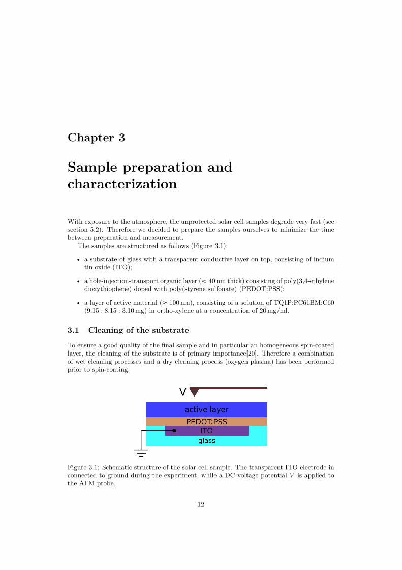
The samples are structured as follows (Figure 3.1):
• a substrate of glass with a transparent conductive layer on top, consisting of indiumtin oxide (ITO);
• a hole-injection-transport organic layer (≈ 40 nm thick) consisting of poly(3,4-ethylenedioxythiophene) doped with poly(styrene sulfonate) (PEDOT:PSS);
• a layer of active material (≈ 100 nm), consisting of a solution of TQ1P:PC61BM:C60(9.15 : 8.15 : 3.10 mg) in ortho-xylene at a concentration of 20 mg/ml.
3.1 Cleaning of the substrate
To ensure a good quality of the final sample and in particular an homogeneous spin-coatedlayer, the cleaning of the substrate is of primary importance[20]. Therefore a combinationof wet cleaning processes and a dry cleaning process (oxygen plasma) has been performedprior to spin-coating.
Figure 3.1: Schematic structure of the solar cell sample. The transparent ITO electrode inconnected to ground during the experiment, while a DC voltage potential V is applied tothe AFM probe.
12

CHAPTER 3. SAMPLE PREPARATION AND CHARACTERIZATION 13
Firstly, the ITO-on-glass substrate was rubbed with a solution of standard laboratorysoap (Extran® MA 03) in de-ionized water and a clean-room tissue.
Secondly, two steps of 5 minutes sonication at middle-power (power setting 5 out of 9in a VWR Ultrasonic Cleaner) in acetone and isopropyl alcohol (IPA) were performed.
Finally, the sample was treated with oxygen plasma at a O2 partial pressure of 30 mTorrand a gas flux of 20 sccm for 10 min, with a RF power of 30 W (Oxford Plasmalab).
After each wet cleaning step, the sample was dipped into de-ionized water. Before theoxygen plasma treatment, the sample was blown dry with a nitrogen gun.
3.2 Spin-coating
Spin-coating of both the PEDOT:PSS layer and the active layer have been performed witha two step spinning process to ensure uniformity of the layers.
In particular, for the PEDOT:PSS layer:
• 200µl of solution were spread over the substrate while this was rotating at about 500 rpmfor 10 s;
• the layer was spin-coated at about 3000 rpm for 60 s;
• the sample (ITO-on-glass substrate + PEDOT:PSS) was baked at 120 °C for 10 min.
After the baking, the active layer was spin-coated:
• 40µl of solution were spread over the substrate while this was rotating at about 500 rpmfor 10 s;
• the layer was spin-coated at about 3000 rpm for 120 s.
3.3 AFM images and force reconstruction
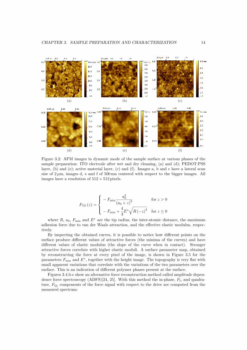
After every step of the sample preparation, AFM scans in dynamic mode were performedto investigate the sample surface and to assess the correct preparation of the solar cell.The recorded topographies, Figure 3.2, showed similar features to that reported in theliterature[21, 22].
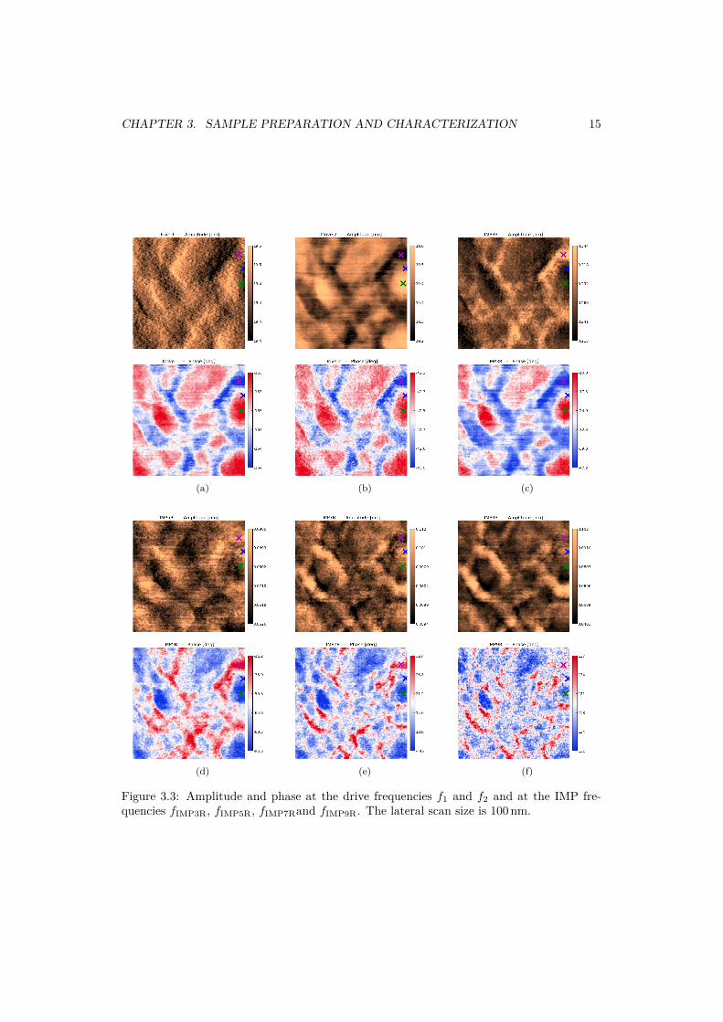
Figure 3.3 shows an AFM image obtained in Intermodulation spectroscopy mode. Thelateral scan size is 100 nm and the resolution is 256 × 256 pixels. After the acquisition theimage was smoothed with a two dimensional Gaussian filter with σx = σy = 1 to lowerthe noise level. The response amplitude and phase at the two drive frequencies f1 and f2are shown, together with the amplitude and phases of the third, fifth, seventh and ninthorder intermodulation products occurring on the right side of the frequency spectrum atfrequencies fIMP3R = f2+df , fIMP5R = f2+2df , fIMP7R = f2+3df , and fIMP9R = f2+4dfwhere df = f2 − f1 represents both the separation between the two drive frequencies andthe lock-in measurement bandwidth.
Force reconstruction with the Intermodulation AFM technique has also been performedon the final sample (Figure 3.4). ImAFM allows for different force reconstruction algo-rithms. Figure 3.4.a shows force curves on different points of the surface obtained with amodel based force reconstruction: a least-squares optimization algorithm is used to fit theparameters of the Derjaguin-Muller-Toropov (DMT) model to the measured intermodula-tion spectrum[23]. The DMT model hypothesizes a tip-surface force FTS as a function ofdistance z of the form:
CHAPTER 3. SAMPLE PREPARATION AND CHARACTERIZATION 14
(a) (b) (c)
(d) (e) (f)
Figure 3.2: AFM images in dynamic mode of the sample surface at various phases of thesample preparation: ITO electrode after wet and dry cleaning, (a) and (d); PEDOT:PSSlayer, (b) and (e); active material layer, (c) and (f). Images a, b and c have a lateral scansize of 2µm, images d, e and f of 500 nm centered with respect to the bigger images. Allimages have a resolution of 512× 512 pixels.
FTS (z) =
− Fmin
a20
(a0 + z)2 for z > 0
− Fmin + 43E∗√R (−z)3 for z ≤ 0
where R, a0, Fmin and E∗ are the tip radius, the inter-atomic distance, the maximumadhesion force due to van der Waals attraction, and the effective elastic modulus, respec-tively.
By inspecting the obtained curves, it is possible to notice how different points on thesurface produce different values of attractive forces (the minima of the curves) and havedifferent values of elastic modulus (the slope of the curve when in contact). Strongerattractive forces correlate with higher elastic moduli. A surface parameter map, obtainedby reconstructing the force at every pixel of the image, is shown in Figure 3.5 for theparameters Fmin and E∗, together with the height image. The topography is very flat withsmall apparent variations that correlate with the variations of the two parameters over thesurface. This is an indication of different polymer phases present at the surface.
Figures 3.4.b-c show an alternative force reconstruction method called amplitude depen-dence force spectroscopy (ADFS)[24, 25]. With this method the in-phase, FI, and quadra-ture, FQ, components of the force signal with respect to the drive are computed from themeasured spectrum:
CHAPTER 3. SAMPLE PREPARATION AND CHARACTERIZATION 15
(a) (b) (c)
(d) (e) (f)
Figure 3.3: Amplitude and phase at the drive frequencies f1 and f2 and at the IMP fre-quencies fIMP3R, fIMP5R, fIMP7Rand fIMP9R. The lateral scan size is 100 nm.

CHAPTER 3. SAMPLE PREPARATION AND CHARACTERIZATION 16
(a) (b) (c)
Figure 3.4: Force reconstruction at different locations on the surface. The color of the curvesin (a), (b) and (c) refers to the color of the crosses in Figure 3.3. (a) force reconstructionassuming a DMT force model; (b) force reconstruction with the ADFS algorithm; (c) forcecomponents in-phase, FI, and quadrature, FQ, with the cantilever motion.
(a) (b) (c)
Figure 3.5: Surface parameter maps of the force, obtained assuming a DMT force model.(a) maximum adhesion force due to van der Waals attraction in nN; (b) effective elasticmodulus in GPa; (c) topography image, height in nm.
CHAPTER 3. SAMPLE PREPARATION AND CHARACTERIZATION 17
FI = 1T
ˆ T
0Fts (z (t) , z (t))
(z (t)− h
A
)dt
FQ = 1T
ˆ T
0Fts (z (t) , z (t))
(z (t)−ω0A
)dt
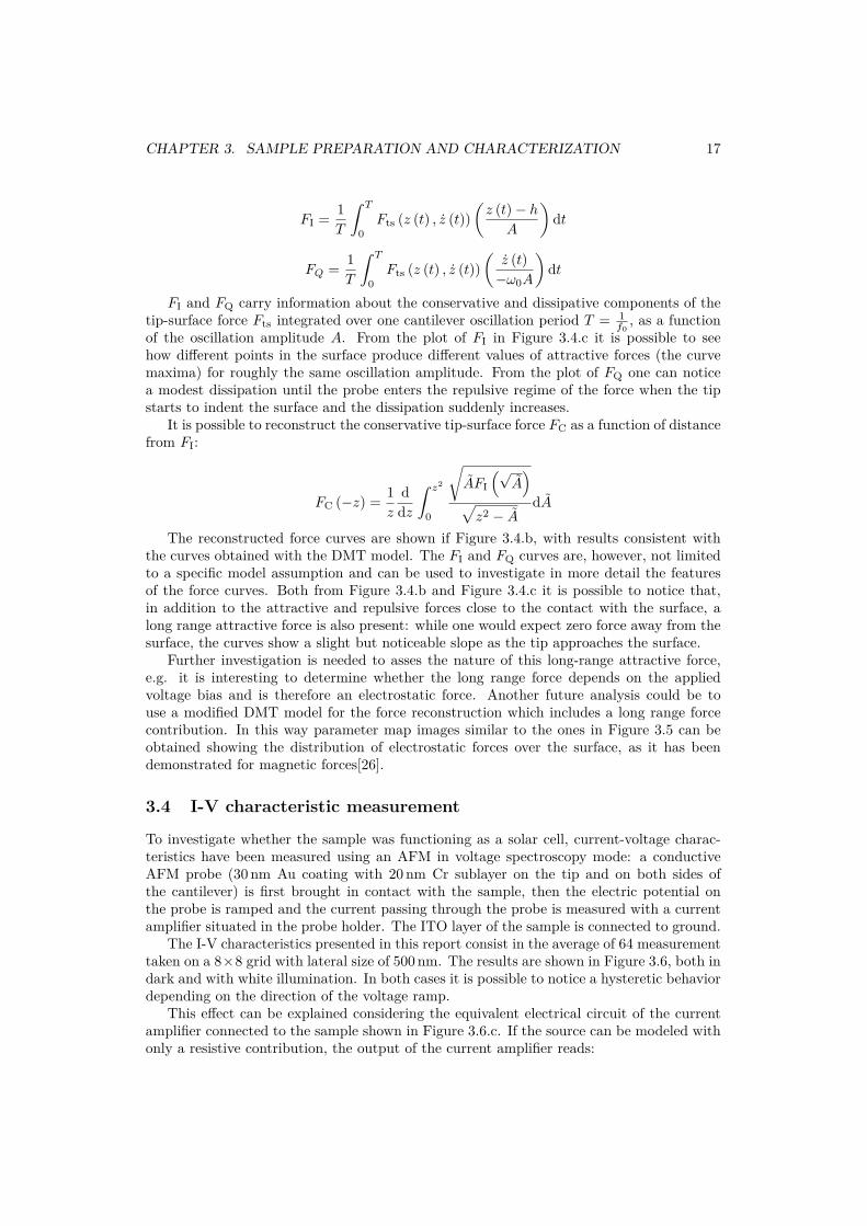
FI and FQ carry information about the conservative and dissipative components of thetip-surface force Fts integrated over one cantilever oscillation period T = 1
f0, as a function
of the oscillation amplitude A. From the plot of FI in Figure 3.4.c it is possible to seehow different points in the surface produce different values of attractive forces (the curvemaxima) for roughly the same oscillation amplitude. From the plot of FQ one can noticea modest dissipation until the probe enters the repulsive regime of the force when the tipstarts to indent the surface and the dissipation suddenly increases.
It is possible to reconstruct the conservative tip-surface force FC as a function of distancefrom FI:
FC (−z) = 1z
ddz
ˆ z2
0
√AFI
(√A)
√z2 − A
dA
The reconstructed force curves are shown if Figure 3.4.b, with results consistent withthe curves obtained with the DMT model. The FI and FQ curves are, however, not limitedto a specific model assumption and can be used to investigate in more detail the featuresof the force curves. Both from Figure 3.4.b and Figure 3.4.c it is possible to notice that,in addition to the attractive and repulsive forces close to the contact with the surface, along range attractive force is also present: while one would expect zero force away from thesurface, the curves show a slight but noticeable slope as the tip approaches the surface.
Further investigation is needed to asses the nature of this long-range attractive force,e.g. it is interesting to determine whether the long range force depends on the appliedvoltage bias and is therefore an electrostatic force. Another future analysis could be touse a modified DMT model for the force reconstruction which includes a long range forcecontribution. In this way parameter map images similar to the ones in Figure 3.5 can beobtained showing the distribution of electrostatic forces over the surface, as it has beendemonstrated for magnetic forces[26].
3.4 I-V characteristic measurement
To investigate whether the sample was functioning as a solar cell, current-voltage charac-teristics have been measured using an AFM in voltage spectroscopy mode: a conductiveAFM probe (30 nm Au coating with 20 nm Cr sublayer on the tip and on both sides ofthe cantilever) is first brought in contact with the sample, then the electric potential onthe probe is ramped and the current passing through the probe is measured with a currentamplifier situated in the probe holder. The ITO layer of the sample is connected to ground.
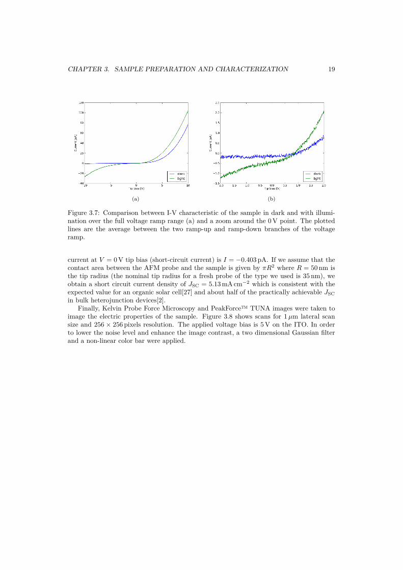
The I-V characteristics presented in this report consist in the average of 64 measurementtaken on a 8×8 grid with lateral size of 500 nm. The results are shown in Figure 3.6, both indark and with white illumination. In both cases it is possible to notice a hysteretic behaviordepending on the direction of the voltage ramp.
This effect can be explained considering the equivalent electrical circuit of the currentamplifier connected to the sample shown in Figure 3.6.c. If the source can be modeled withonly a resistive contribution, the output of the current amplifier reads:

CHAPTER 3. SAMPLE PREPARATION AND CHARACTERIZATION 18
(a) (b) (c)
Figure 3.6: I-V characteristic measurements in dark (a), and with illumination (b). In bothcases a hysteretic behavior is present when the tip bias is first increased from −10 V to 10 V(blue line) and then decreased back to −10 V (green line). The electrical scheme of themeasurement is shown, with both the source resistance and capacitance, (c).
VOUT = RFEEDBACK
RSOURCEVBIAS
From the measured data, when VBIAS = 9.983 V the current amplifiers measures, indark, IOUT = VOUT/RFEEDBACK = 76.66 pA. We can then get a rough estimation for thevalue of RSOURCE ≈ VBIAS/IOUT = 130.2 GΩ.
For such a big resistance, it is common to see the effect of a parasite capacitance inparallel with the source resistance, denoted by CS in Figure 3.6.c. The output of thecurrent amplifier is:
VOUT = RFEEDBACK
RSOURCEVBIAS +RFEEDBACKCSOURCE
dVBIAS
dtThe effect of the source capacitance is a current offset. Its magnitude depends on the
speed of the voltage ramp and its sign on the voltage ramp direction. Assuming RSOURCEdepends only on the voltage bias and not on its derivative, we can estimate the sourcecapacitance by taking the average differential signal between the ramp-up and ramp-downmeasurements:
ID = IUP − IDOWN
2Knowing that the voltage bias ramps from −10 V to 10 V in half a second, we get:
CSOURCE ≈〈ID〉
dV/dt = 15.18 pA40 V/s = 379.5 fF
which is a reasonable value of source capacitance. From now on, in our analysis we will usethe common mode signal between the ramp-up and ramp-down measurement to get rid ofthe current offset due to the source capacitance:
IC = IUP + IDOWN
2We compare the behavior of the solar cell in dark and under white illumination by
plotting IC vs. VBIAS. From Figure 3.7 it is possible to distinguish a clear dependence ofthe measured current on the presence of illumination. Under illumination the measured
CHAPTER 3. SAMPLE PREPARATION AND CHARACTERIZATION 19
(a) (b)
Figure 3.7: Comparison between I-V characteristic of the sample in dark and with illumi-nation over the full voltage ramp range (a) and a zoom around the 0 V point. The plottedlines are the average between the two ramp-up and ramp-down branches of the voltageramp.
current at V = 0 V tip bias (short-circuit current) is I = −0.403 pA. If we assume that thecontact area between the AFM probe and the sample is given by πR2 where R = 50 nm isthe tip radius (the nominal tip radius for a fresh probe of the type we used is 35 nm), weobtain a short circuit current density of JSC = 5.13 mA cm−2 which is consistent with theexpected value for an organic solar cell[27] and about half of the practically achievable JSCin bulk heterojunction devices[2].
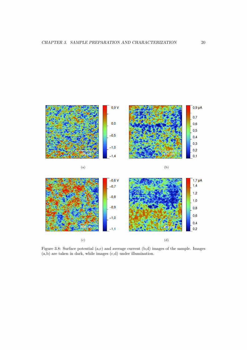
Finally, Kelvin Probe Force Microscopy and PeakForce™ TUNA images were taken toimage the electric properties of the sample. Figure 3.8 shows scans for 1µm lateral scansize and 256 × 256 pixels resolution. The applied voltage bias is 5 V on the ITO. In orderto lower the noise level and enhance the image contrast, a two dimensional Gaussian filterand a non-linear color bar were applied.
CHAPTER 3. SAMPLE PREPARATION AND CHARACTERIZATION 20
(a) (b)
(c) (d)
Figure 3.8: Surface potential (a,c) and average current (b,d) images of the sample. Images(a,b) are taken in dark, while images (c,d) under illumination.

Chapter 4
Experimental set-up
4.1 Bottom-up illumination
Two different kinds of set-ups have been used to perform measurements under controlledillumination: bottom-up illumination and total internal reflection illumination. In bothcases the light source was a commercial white LED (Sloan Precision Optoelectronics L3-W37N-BVW) connected in series with a 140 Ω resistor and driven by an arbitrary waveformgenerator (Agilent 33250A, 50 Ω output resistance).
A cylinder of poly(methyl methacrylate) (PMMA) was manufactured by our universitycampus workshop. The PMMA cylinder allows to mount the sample on the AFM stageusing the vacuum system, while illuminating the scan area with the LED from beneathwith a high intensity (see Figure 4.1.b). The advantage of this set-up is the very high lightintensity that is possible to achieve on the scan area with a commercial LED. On the otherhand, light pressure on the cantilever and cantilever heating become important and affectthe measurement (see section 5.1).
(a) (b)
Figure 4.1: Bottom-up set-up: (a) schematic representation of the sample holder and illu-mination scheme; (b) picture of the set-up.
21

CHAPTER 4. EXPERIMENTAL SET-UP 22
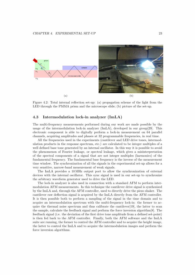
4.2 Total internal reflection illumination
A prism of PMMA was also manufactured by our university campus workshop. The prismallows to couple the light from the LED inside a standard microscope slide using the totalinternal reflection effect, as it is commonly done in the optical microscopy technique calledtotal internal reflection flourescence (TIRF)[28]. The sample was then situated on top ofthe microscope slide (Figure 4.2). To achieve better optical coupling between the prismand the microscope slide and between the microscope slide and the sample, a thin layer ofde-ionized water was put at the two interfaces.
While the confinement of the light intensity inside the microscope slide and the samplesubstrate allow for a measurement not affected by illumination of the cantilever body,we found that the light intensity in the active layer was not high enough to produce anappreciable electrostatic force on the cantilever.
Calculation of the emission angleAn important feature of the prism is the angle between the emission axis of the LED andthe normal to the microscope slide surface: this angle determines the fraction of the emittedintensity coupled inside the microscope slide by the total internal reflection effect.
Total internal reflection occurs when the incident angle θi is greater than the criticalangle θc, defined as the incident angle at which the transmitted angle θt is equal to π
2 .According to Snell’s law:
n1 sin θi = n2 sin θt
In our case n1 = 1.518 is the refractive index of the microscope slide, θi = θc, n2 =1.000277 ≈ 1 is the refractive index of air and θt = π
2 . Solving for sin θc we get:
sin θc = 1n1
Since the light emitted from the LED first travels in PMMA, the change in propagationangle due to refraction from PMMA to glass must be taken into account. Using againSnell’s law:
n3 sin θe = n1 sin θc
where n3 = 1.4896 is the refractive index of PMMA and θe is the emission angle in thePMMA. The light ray propagates in the microscope slide at the critical angle θc if it travelsin the PMMA at an angle:
θe = arcsin(n1
n3sin θc
)= arcsin
(1n3
)≈ 42.17°
It is worth noticing that the condition for total internal reflection in our set-up does notdepend on the microscope slide refractive index, but only on that of the PMMA prism.
According to the LED specifications the viewing angle is 2θ1/2 = 20°, meaning thatthe emitted intensity drops to 1/2 of its maximum at 10° from the emission axis. To beable to confine a bigger portion of the emitted intensity in the microscope slide with totalinternal reflection, additional 10° have been added to the previously calculated emissionangle θe ≈ 42.17° in the design of the prism (Figure 4.2).
CHAPTER 4. EXPERIMENTAL SET-UP 23
(a) (b)
Figure 4.2: Total internal reflection set-up: (a) propagation scheme of the light from theLED through the PMMA prism and the microscope slide; (b) picture of the set-up.
4.3 Intermodulation lock-in analyzer (ImLA)
The multi-frequency measurements performed during our work are made possible by theusage of the intermodulation lock-in analyzer (ImLA), developed in our group[29]. Thiselectronic component is able to digitally perform a lock-in measurement on 64 parallelchannels, acquiring amplitudes and phases at 32 programmable frequencies, in real time.
All the frequencies used in the experiments (cantilever and LED drive tones, intermod-ulation products in the response spectrum, etc.) are calculated to be integer multiples of awell defined base tone generated by an internal oscillator. In this way it is possible to avoidthe phenomenon of Fourier leakage, or spectral leakage, which gives a misinterpretationof the spectral components of a signal that are not integer multiples (harmonics) of thefundamental frequency. The fundamental base frequency is the inverse of the measurementtime window. The synchronization of all the signals in the experimental set-up allows for avery sensitive, narrow-band measurement of weak signals.
The ImLA provides a 10 MHz output port to allow the synchronization of externaldevices with the internal oscillator. This sync signal is used in our set-up to synchronizethe arbitrary waveform generator used to drive the LED.
The lock-in analyzer is also used in connection with a standard AFM to perform inter-modulation AFM measurements. In this technique the cantilever drive signal is synthesizedby the ImLA and, through the AFM controller, used to directly drive the piezo shaker. Thecantilever raw deflection signal is acquired by the ImLA directly from the AFM controller.It is then possible both to perform a sampling of the signal in the time domain and toacquire an intermodulation spectrum with the multi-frequency lock-in: the former to ac-quire the thermal noise spectrum and thus calibrate the cantilever[19], the latter to scanthe sample, calculate the feedback signal and perform the force inversion algorithm[8]. Thefeedback signal (i.e. the deviation of the first drive tone amplitude from a defined set-point)is then fed back to the AFM controller. Finally, both the AFM software and the ImLAsuite are running, the former to control the AFM controller and to acquire the height image,the latter to control the ImLA and to acquire the intermodulation images and perform theforce inversion algorithms.

Chapter 5
Challenges
5.1 Effect of direct light on the cantilever
To investigate the effect of the light coming from the LED shining directly onto the can-tilever, simple calculations to estimate the radiant flux (also known as radiant power) andthe radiation force on the surface of the cantilever have been performed.
From the LED specifications, the light emission has a peak at λ = 461 nm and a nominalluminous intensity at 20 mA forward current equal to IV = 13350 mcd at normal emission.Knowing the luminous efficacy at the wavelength of interest K = 42.47 cd sr/W, we get theradiant intensity:
IE = IVK
= 314.34 mWsr
Estimating the solid angle with which the cantilever is seen from the LED as the ratiobetween the area of the cantilever and the tip-LED distance squared we get:
Ω ≈ Acantileverd2 = 125× 40µm2
2.62 mm2 = 7.396 · 10−4 sr
Neglecting the change in radiant intensity over the solid angle, the radiant flux on thecantilever results:
ΦE = IE · Ω = 2.325 · 10−4 Wand thus the force on the cantilever due to the radiation pressure, assuming the light is
completely absorbed:
F = ΦEc
= 7.76 · 10−13 N (5.1)
where c is the speed of light in vacuum. If the light were completely reflected, the forcewould be twice this value. For comparison, the thermal noise force spectrum integratedover the mechanical resonance of the cantilever is typically of the order of 750 · 10−15 N.The radiation force 5.1 is then of the same order of magnitude as the thermal noise force,which is measurable with our apparatus.
Measurement and analysisTo experimentally investigate this phenomenon, a frequency sweep has been performed. Inthe experiment the frequency of the drive of the LED, shining directly onto the cantilever,
24

CHAPTER 5. CHALLENGES 25
(a) (b)
Figure 5.1: Cantilever response at different light illumination frequencies: (a) raw data; (b)data corrected for phase shift and direct pick-up.
is changed in a 15 kHz range around the cantilever mechanical resonance and for eachfrequency the amplitude and phase of the cantilever response at the same frequency aremeasured.
Figure 5.1-a shows the raw data obtained. The amplitude and phase of the cantileverresponse clearly depend on the LED drive frequency and a feature at the cantilever resonancefrequency (previously measured to be 429746 Hz) is visible.
From figure 5.1-a it is possible to notice a strong amplitude background, due to directpick-up of the LED light into the AFM photo-detector, and a linear phase shift due toa constant time delay in our set-up. Figure 5.1-b shows the data obtained from the rawmeasurement by compensating for the two effects as follows.
Firstly, a linear phase change was fitted to the measured phase in the first 5.5 kHz band(before the resonance peak) obtaining the function θfit (f). The fitted phase θfit (f) wasthen subtracted from the measured complex data x (f):
x′ (f) = x (f)eiθfit(f) eiθfit(fstart)
where fstart is the initial measurement frequency. This operation eliminates the linearphase shift, however both the real and imaginary part of x′ (f) still present a constantbackground due to direct light pick-up.
Secondly, a linear function was fitted to both the real and imaginary part of x′ (f) sepa-rately in the first 5.5 kHz band (before the resonance peak) obtaining the functions afit (f)and bfit (f). The fitted functions afit (f) and bfit (f) were then subtracted from the phaseshift corrected data x′ (f):
x′′ (f) = x′ (f)− afit (f)− ibfit (f)
The corrected data in figure 5.1-b show a clear resonance peak in amplitude, indicatingthat the light is directly driving the cantilever. Moreover, a 90° phase shift around resonanceis shown in the phase signal which eliminates the possibility that the peak in amplitude isdue to thermal fluctuations, where no coherent phase would be measured.

CHAPTER 5. CHALLENGES 26
5.2 Degradation of the sample
Stability and degradation issues of polymer solar cells are well known and are nowadays avery active field of study[30]. When exposed to oxygen and water (i.e. to a non controlledatmosphere), unprotected solar cell samples undergo degradation mainly due to diffusion ofthese species in the whole device and due to oxidation of its layers, which is enhanced by ex-posure to light. The degradation manifests within hours of exposure and is mainly detectedas a decrease in the photo-current and an increase in the internal device resistivity[31].
For this reason and in order to be able to perform measurements on freshly preparedsamples, we decided to prepare the solar cells by ourselves despite having no previousexperience. Previously (as in the measurement of Section 2.4) the samples were preparedat the Center of Organic Electronics at Linköping University, led by Prof Olle Inganäs.Switching to a local solution brought the time between sample preparation and measurementfrom several days down to less than one hour. The sample preparation is described inChapter 3.

Chapter 6
Conclusions
Despite the proposed method was first demonstrated by a computer simulation and then itsconcept validated with electrostatic force microscopy, the intermodulation spectrum due tophoto-induced electrostatic forces between the AFM probe and an organic solar cell couldnot be measured experimentally. The most important improvement points for the future ofthis technique are the illumination of the sample and the sample preparation.
The bottom-up illumination set-up provides high light intensity on the scan area, buta big amount of light irradiates the cantilever causing intermodulation products to ariseregardless of the sample characteristics. The total internal reflection set-up presents theopposite situation: the confinement of the light beam inside the microscope slide preventsthe cantilever from experiences forces due to direct illumination, but the light intensity inthe active layer is not high enough to produce a measurable signal. This is probably dueto the relatively broad divergence of the light emitted from the LED. A possible solutionto the illumination problem is to use a confocal microscope to focus the light from an LEDor a modulable laser diode on a small spot on the sample surface: in this way a high lightintensity is granted in the active layer while a relative low intensity can be kept on the outof focus AFM cantilever.
To ensure a longer lifetime of the prepared solar cells and thus a more efficient chargegeneration in the active layer, the samples should be prepared, stored and analyzed in inertatmosphere, e.g. in a nitrogen filled glove box.
Finally, the problem of imaging photo-induced charges on a organic material with in-termodulation can be shifted from measuring electrostatic forces to measuring current. Bymodulating the light intensity at frequency fL close to the cantilever drive fDRIVE, a lowfrequency intermodulation spectrum can be measured in the electric current flowing throughthe AFM probe as it taps on the surface (at frequencies n (fL − fDRIVE) , n = 1, 2, . . .).This would down shift the current signal to frequencies measurable by the current am-plifier(typically below a few hundred Hertz due to the very high gains used). The inter-modulation lock-in analyzer we are currently using is however not able to acquire signalat low frequencies (below 1 kHz) and this technique must wait for future upgrades of ourelectronics.
27

Acknowledgements
This project has lasted only a few months, during which I faced several challenges anddeveloped myself a lot. This would not have been possible without the help of some peopleI would like to acknowledge.
First of all, I would like to thank Prof. David Haviland for giving me the opportunityto join the Nanostructure Physics group at KTH and to challenge myself with this new andfascinating research project. Special thanks also to my supervisor Daniel Forchheimer, myroommate Dr. Daniel Platz, and my colleague Per-Anders Thorén for welcoming me into thegroup and helping me along the way, being always available to discuss technical issues andscientific results, and to have a nice chat. I would like to thank also all the NanostructurePhysics group at KTH for creating such a friendly and productive environment.
Finally, the biggest acknowledgement goes to my family and my friends. Thank you allfor always supporting and believing in me.
Riccardo BorganiStockholm, January 2014
28

Bibliography
[1] H. Hoppe, and N.S. Sariciftci. Organic solar cells: An overview. Journal of MaterialsResearch, 19(07), 1924–1945 (2004).
[2] G. Dennler, M.C. Scharber, and C.J. Brabec. Polymer-Fullerene Bulk-HeterojunctionSolar Cells. Advanced Materials, 21(13), 1323–1338 (2009).
[3] G. Binnig, C.F. Quate, and C. Gerber. Atomic Force Microscope. Physical ReviewLetters, 56(9), 930-933 (1986).
[4] F. Ohnesorge, and G. Binnig. True Atomic Resolution by Atomic Force MicroscopyThrough Repulsive and Attractive Forces. Science, 260(5113), 1451-1456(1993).
[5] S. Guo, S.V. Kalinin, and S. Jesse. Open-loop band excitation Kelvin probe force mi-croscopy. Nanotechnology, 23(12), 125704 (2012).
[6] R. Garca, M. Calleja, and H. Rohrer. Patterning of silicon surfaces with noncontactatomic force microscopy: Field-induced formation of nanometer-size water bridges.Journal of Applied Physics, 86(4), 1898-1903 (1999).
[7] Q. Zhong, D. Inniss, K. Kjoller, and V.B. Elings. Fractured polymer/silica fiber surfacestudied by tapping mode atomic force microscopy. Surface Science, 290(1–2), L688-L692(1993).
[8] D. Platz, E.A. Tholén,D. Pesen, and D.B. Haviland. Intermodulation atomic forcemicroscopy. Applied Physics Letters, 92, 153106 (2008).
[9] D. Platz, D. Forchheimer, E.A. Tholén, and D.B. Haviland. The role of nonlineardynamics in quantitative atomic force microscopy. Nanotechnology, 23(26), 265705(2012).
[10] J. Legleiter, M. Park, B. Cusick, and T. Kowalewski. Scanning probe acceleration mi-croscopy (SPAM) in fluids: Mapping mechanical properties of surfaces at the nanoscale.Proc. Natl. Acad. Sci. U.S.A., 103(13), 4813-4818 (2006).
[11] M. Stark, R.W. Stark, W.M. Heckl, and R. Guckenberger. Inverting dynamic forcemicroscopy: From signals to time-resolved interaction forces. Proc. Natl. Acad. Sci.U.S.A., 99(13), 8473-8478 (2002).
[12] O. Sahin, S. Magonov, C. Su, C.F. Quate, and O. Solgaard. An atomic force microscopetip designed to measure time-varying nanomechanical forces. Nature nanotechnology,2(8), 507–14 (2007).
29

BIBLIOGRAPHY 30
[13] B. Moores, F. Hane, L. Eng, and Z. Leonenko. Kelvin probe force microscopy in ap-plication to biomolecular films: Frequency modulation, amplitude modulation, and liftmode. Ultramicroscopy, 110(6), 708-711 (2010).
[14] M.J. Cadena, R. Misiego, K.C. Smith, A. Avila, B. Pipes, R. Reifenberger, and A.Raman. Sub-surface imaging of carbon nanotube-polymer composites using dynamicAFM methods. Nanotechnology, 24(13), 135706 (2013).
[15] T.W. Kelley, E. Granstrom, and C.D. Frisbie. Conducting Probe Atomic Force Mi-croscopy: A Characterization Tool for Molecular Electronics. Advanced Materials,11(3), 261-264 (1999).
[16] C.D. Coffey, and D.S. Ginger. Time-resolved electrostatic force microscopy of polymersolar cells. Nature materials, 5(9), 735–740 (2006).
[17] S. Hudlet, M. Saint Jean, C. Guthmann, and J. Berger. Evaluation of the capacitiveforce between an atomic force microscopy tip and a metallic surface. The EuropeanPhysical Journal B, 2(1), 5–10 (1998).
[18] R. Giridharagopal, G.E. Rayermann, G. Shao, D.T. Moore, G. Obadiah, A.F. Tillack,D.J. Masiello, and D.S. Ginger. Submicrosecond time resolution atomic force mi-croscopy for probing nanoscale dynamics. Nano letters, 12(2), 893–898 (2012).
[19] M.J. Higgins, R. Proksch, J.E. Sader, M. Polcik, S. Mc Endoo, J.P. Cleveland, andS.P. Jarvis. Noninvasive determination of optical lever sensitivity in atomic force mi-croscopy. Review of Scientific Instruments, 77(1), 013701 (2006).
[20] J. S. Kim, M. Granström, R.H. Friend, N. Johansson, W.R. Salaneck, R. Daik, W.J.Feast, and F. Cacialli. Indium–tin oxide treatments for single- and double-layer poly-meric light-emitting diodes: The relation between the anode physical, chemical, andmorphological properties and the device performance. Journal of Applied Physics, 84,6859-6870 (1998).
[21] Y. Shigesato, R. Koshi-ishi, T. Kawashima, and J. Ohsako. Early stages of ITO depo-sition on glass or polymer substrates. Vacuum, 59(2–3), 614-621 (2000).
[22] C.S. Suchand Sangeeth, M. Jaiswal and R. Menon. Correlation of morphology andcharge transport in poly(3,4-ethylenedioxythiophene)–polystyrenesulfonic acid (PE-DOT–PSS) films. Journal of Physics: Condensed Matter, 21(7), 072101 (2009).
[23] D. Forchheimer, D. Platz, E.A. Tholén, and D.B. Haviland. Model-based extractionof material properties in multifrequency atomic force microscopy. Physical Review B,85(19), 195449 (2012).
[24] D. Platz, D. Forchheimer, E.A. Tholén, and D.B. Haviland. Interpreting motion andforce for narrow-band intermodulation atomic force microscopy. Beilstein journal ofnanotechnology, 4, 45–56 (2013).
[25] D. Platz, D. Forchheimer, E.A. Tholén, and D.B. Haviland. Interaction imaging withamplitude-dependence force spectroscopy. Nature communications, 4, 1360 (2013).
[26] D. Forchheimer, D. Platz, E.A. Tholén, and D.B. Haviland. Simultaneous imaging ofsurface and magnetic forces. Applied Physics Letters, 103(1), 013114 (2013).
BIBLIOGRAPHY 31
[27] M. Glatthaar, M. Riede, N. Keegan, K. Sylvester-Hvid, B. Zimmermann, M. Nigge-mann, A. Hinsch, and A. Gombert. Efficiency limiting factors of organic bulk hetero-junction solar cells identified by electrical impedance spectroscopy. Solar Energy Mate-rials and Solar Cells, 91(5), 390-393 (2007).
[28] D. Axelrod. Total internal reflection fluorescence microscopy in cell biology. Methodsin enzymology, 361(2), 1–33 (2003).
[29] E.A. Tholén, D. Platz, D. Forchheimer, V. Schuler, M.O. Tholén, C. Hutter, andD.B. Haviland. Note: The intermodulation lockin analyzer. The Review of scientificinstruments, 82(2), 026109 (2011).
[30] M. Jørgensen, K. Norrman, and F.C. Krebs. Stability/degradation of polymer solarcells. Solar Energy Materials and Solar Cells, 92(7), 686-714 (2008).
[31] H. Neugebauer, C. Brabec, J.C. Hummelen, and N.S. Sariciftci. Stability and pho-todegradation mechanisms of conjugated polymer/fullerene plastic solar cells. Solar En-ergy Materials and Solar Cells, 61(1), 35-42 (2000).