a nonlinear, geometric hall e ect without magnetic eld
TRANSCRIPT
A nonlinear, geometric Hall effect without magneticfield
Nicholas B. Schade,1∗, David I. Schuster,2 and Sidney R. Nagel1
1Department of Physics and the James Franck and Enrico Fermi Institutes,
University of Chicago, Chicago, IL 60637, USA2Department of Physics and the James Franck Institute,
University of Chicago, Chicago, IL 60637, USA
∗To whom correspondence should be addressed; E-mail: [email protected].
Abstract
The classical Hall effect, the traditional means of determining charge-carrier signand density in a conductor, requires a magnetic field to produce transverse voltagesacross a current-carrying wire. We show that along curved paths – without any mag-netic field – geometry alone can produce nonlinear transverse potentials that reflectthe charge-carrier sign and density. We demonstrate this effect in curved graphenewires where the transverse potentials are consistent with the doping and changepolarity as we switch the carrier sign. In straight wires, we measure transversepotential fluctuations with random polarity demonstrating that the current followsa complex, tortuous path. This geometrically-induced potential offers a sensitivecharacterization of inhomogeneous current flow in thin films.
In 1879, Edwin Hall discovered that a transverse potential appears across a current-
carrying wire placed in a magnetic field [1]. Physics instructors traditionally teach the Hall
effect when the magnetic field is first presented in introductory electricity and magnetism
as the way to distinguish the sign of the charge carriers in a conductor [2]. Indeed, the
Hall effect is an efficient way to disentangle the role of electron and hole conduction in
semiconductors [3] and is commonly used to measure the magnitude of magnetic fields [4].
1
arX
iv:1
902.
0344
5v1
[co
nd-m
at.m
es-h
all]
9 F
eb 2
019
Here we present a different mechanism using geometry alone, without a magnetic field, to
produce a transverse voltage that also reflects the sign and density of the charge carriers.
A current traveling through a curved wire must undergo centripetal acceleration to follow
the curve. This acceleration occurs due to electric fields from charges distributed along
the wire edges; the direction of the field must change with the sign of the carriers. No
magnetic field is necessary.
The transverse voltage that we predict and measure is quadratic in the current. It
is therefore distinct from many linear Hall effects such as the spin- [5], valley- [6], and
anomalous- [7] Hall effects. However, the geometric effect we describe should be contrasted
with predictions [8] and recent measurements of a nonlinear Hall effect in nonmagnetic
bilayer materials such as WTe2 [9].
By 1850, Kirchhoff realized that surface charge distributions are necessary simply to
confine a current inside a wire [10]. Subsequently, the role of surface charges has been
investigated theoretically [11, 12, 13] and experimentally using single-electron transis-
tors [14, 15]. The effect we describe is also related to how currents are confined within
wires. Our experiments show that the effect can be used for sensitively probing non-
homogeneous current flow in thin films as well as systems where magnetic fields do not
occur such as the bulk of a superconductor. While the effect is small, it is measurable even
in bulk conductors. Using graphene wires to optimize the signal, we measure transverse
potentials ≈ 0.5 mV.
In the conventional Hall effect, when an electric current I of charge carriers q passes
through an applied magnetic field B, the carriers experience a magnetic Lorentz force
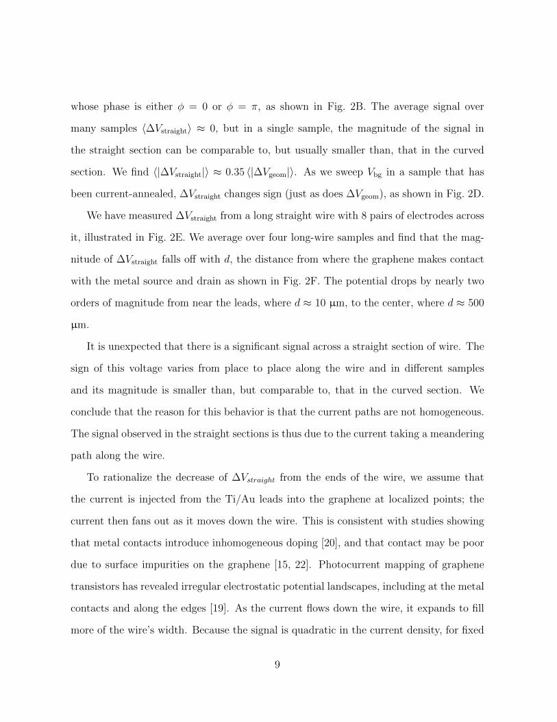
FB = qv ×B. Charge accumulates at the wire edges, as illustrated in Fig. 1A, until the
electric field caused by these charges cancels FB to create a transverse potential difference:
2
VHall =IB
tnq. (1)
Here n is the charge-carrier density and t the wire thickness along the direction of B. A
measurement of VHall determines n and the sign of the charge carriers.
To show that magnetism is not necessary for producing transverse voltages sensitive
to n and the sign of q, we take advantage of surface charge distributions that are a result
of geometry – curvature in the path of the current – rather than magnetic forces. The
surface charges create a transverse component of the electric field and exert a force on
the current such that it follows the wire. For a wire in the shape of a circular arc, the
transverse electric force must point radially towards the circle center to accelerate the
carriers centripetally; this mandates that the direction of the radial electric field (and
thus the potential difference between the wire edges) depends on the sign of the current
carriers, as illustrated in Fig. 1B. The polarity of this potential, analogous to the polarity
of a Hall potential, reveals the sign of the carriers.
Calculating this potential is straightforward. We assume the wire is a semicircular
annulus with inner radius rin and outer radius rout; the wire has a rectangular cross-section
of width w ≡ (rout− rin) and thickness t. We force the radial edges of the half annulus to
be equipotentials, as illustrated in Fig. 1B, with potential difference E = Va− Vb. Due to
azimuthal symmetry, the charges on average follow semicircular trajectories. We assume
that the conductivity σ and carrier density n are uniform and that all charge carriers have
the same mass m and charge q.
Unless the wire is a superconductor, the current density, j(r), is equal to the longitu-
dinal (azimuthal) component of the electric field, Eθ = E/(πr), times the conductivity:
j(r) = σE/(πr). The transverse (i.e., radial) component, Er, provides the force necessary
for the carriers to follow circular paths.
3
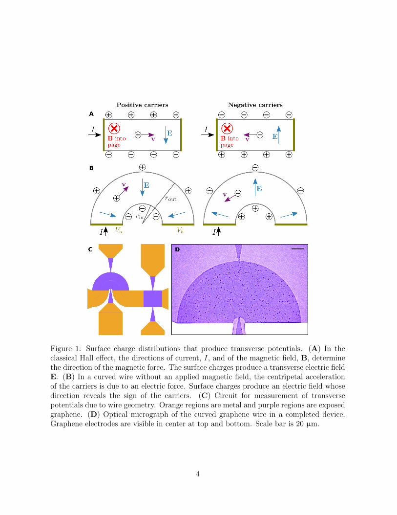
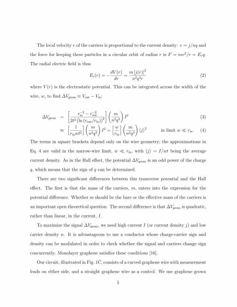
Figure 1: Surface charge distributions that produce transverse potentials. (A) In theclassical Hall effect, the directions of current, I, and of the magnetic field, B, determinethe direction of the magnetic force. The surface charges produce a transverse electric fieldE. (B) In a curved wire without an applied magnetic field, the centripetal accelerationof the carriers is due to an electric force. Surface charges produce an electric field whosedirection reveals the sign of the carriers. (C) Circuit for measurement of transversepotentials due to wire geometry. Orange regions are metal and purple regions are exposedgraphene. (D) Optical micrograph of the curved graphene wire in a completed device.Graphene electrodes are visible in center at top and bottom. Scale bar is 20 µm.
4
The local velocity v of the carriers is proportional to the current density: v = j/nq and
the force for keeping these particles in a circular orbit of radius r is F = mv2/r = Erq.
The radial electric field is thus
Er(r) = −dV (r)
dr=m [j(r)]2
n2q3r(2)
where V (r) is the electrostatic potential. This can be integrated across the width of the
wire, w, to find ∆Vgeom ≡ Vout − Vin:
∆Vgeom =
[r−2in − r−2
out
2t2 (ln (rout/rin))2
](m
n2q3
)I2 (3)
≈[
1
rinwt2
] (m
n2q3
)I2 =
[w
rin
] (m
n2q3
)〈j〉2 in limit w � rin. (4)
The terms in square brackets depend only on the wire geometry; the approximations in
Eq. 4 are valid in the narrow-wire limit, w � rin, with 〈j〉 = I/wt being the average
current density. As in the Hall effect, the potential ∆Vgeom is an odd power of the charge
q, which means that the sign of q can be determined.
There are two significant differences between this transverse potential and the Hall
effect. The first is that the mass of the carriers, m, enters into the expression for the
potential difference. Whether m should be the bare or the effective mass of the carriers is
an important open theoretical question. The second difference is that ∆Vgeom is quadratic,
rather than linear, in the current, I.
To maximize the signal ∆Vgeom, we need high current I (or current density j) and low
carrier density n. It is advantageous to use a conductor whose charge-carrier sign and
density can be modulated in order to check whether the signal and carriers change sign
concurrently. Monolayer graphene satisfies these conditions [16].
Our circuit, illustrated in Fig. 1C, consists of a curved graphene wire with measurement
leads on either side, and a straight graphene wire as a control. We use graphene grown
5
by chemical vapor deposition and transferred by the manufacturer (Graphenea) to a
doped silicon wafer with a 300 nm oxide gap. We use photolithography, electron-beam
evaporation, and plasma etching to pattern the graphene and to place Ti/Au contacts on
it, as shown in Fig. 1D. (See SI for detailed nanofabrication procedure.) We control the
sign and density of the carriers in the graphene by applying a back-gate voltage Vbg to
the silicon. As initially fabricated, the samples are highly doped; we current-anneal [17]
them to cross the Dirac point at Vbg < 100 V.
The fact that the signal is quadratic in the current may be exploited to remove several
potential sources of measurement error. The I2 dependence means that an AC current at
frequency ω produces a transverse potential at frequency 2ω. We use a lock-in amplifier
to measure the potential at 2ω while filtering out potentials at ω. A Hall potential due
to a DC magnetic field, such as that of the earth, will appear at ω and thus can be
safely ignored. The potential drop due to the longitudinal electric field component within
the wire, Eθ, likewise occurs at ω, so we need not worry about imperfect alignment of
transverse measurement leads. By checking that ∆Vgeom is proportional to I2, we ensure
that any 2ω harmonics in the current do not contribute to the signal. Fluctuations in
the conductor’s resistivity due to Joule heating give rise to longitudinal oscillations in the
potential that occur at 3ω and higher harmonics, but not at 2ω. (See SI for details.)
Two extraneous sources of a 2ω signal are due to (i) the Hall voltage from a current-
induced magnetic field and (ii) the Seebeck effect. In the SI we describe how we have
minimized their contribution so that they do not affect our results.
We have measured the potential difference, ∆Vgeom, across the curved wires in our
samples. In all the samples, without any current-annealing and at Vbg = 0, ∆Vgeom is
positive, corresponding to positive charge carriers. This is what is expected in graphene
on a SiO2 substrate [16, 15, 18]. We fit the measured transverse potentials to a power β of
6
the current amplitude, |∆Vgeom| ∝ Iβ, and we find 〈β〉 = 2.00± 0.11. This confirms that
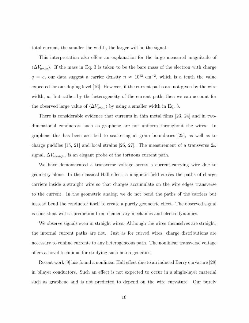
the measured potential rises quadratically with the current, as shown in Fig. 2A. There
is significant scatter in the signal magnitude between samples as shown in Fig. 2B. For a
driving voltage E = 1.00 V, the current is I ≈ 370± 130 µA and the average magnitude
of the signal is 〈∆Vgeom〉 ≈ 0.46 mV. Using Eq. 3 and averaging over the samples, we
measure 〈m/(n2t2q3)〉 ≈ 5× 10⁻⁶ kg m4 C−3.
After current annealing, we can apply a back-gate voltage Vbg to the sample and move
the Fermi level to the other side of the Dirac point where the charge of the carriers has
the opposite sign. We find that ∆Vgeom changes sign at a back-gate voltage close to that
of the conductance minimum, as shown in Fig. 2C. This confirms that this measurement
determines the sign of the charge carriers using only geometry. (This behavior shows
hysteresis with the direction of the Vbg sweep, as is typical of electrical properties of
graphene [18].) Rather than showing a singularity, ∆Vgeom passes smoothly through zero
near the Dirac point. This is consistent with prior observations that in graphene samples
near the Dirac point, inhomogeneities and defects make the graphene behave as a random
assortment of electron and hole puddles rather than as a uniform material with n ≈
0 [15, 19, 20, 21].
Because our samples are thin, the current I is small even though the current density
j is very large. Therefore, the magnitude of the Hall-effect contribution from a current-
induced magnetic field should be (see Fig. S1) at least 20 times smaller than the signal
we observe and the prediction of Eq. 3. We have also checked (see SI) that ∆Vstraight is
not due to the Seebeck effect by varying the length of the graphene voltage-measuring
leads.
The sign of the potential difference, ∆Vstraight, between the two sides of the straight
wire, is not picked out by the curvature of the wire. However, we still find a signal
7
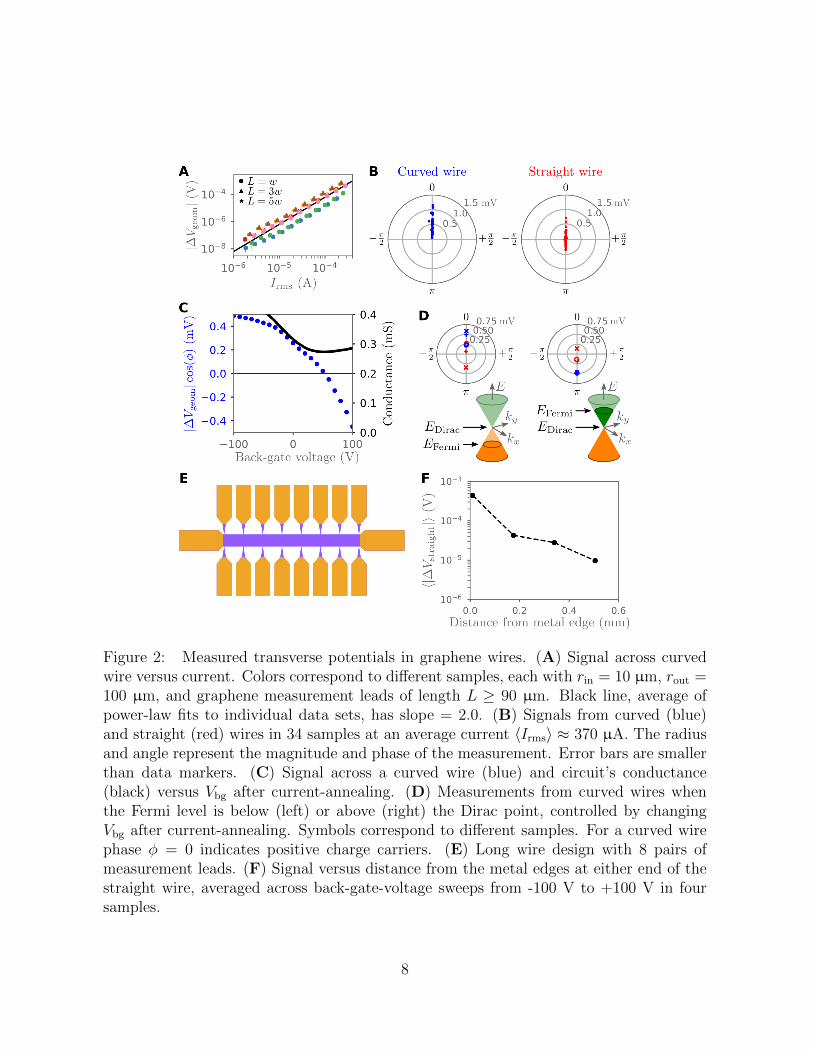
Figure 2: Measured transverse potentials in graphene wires. (A) Signal across curvedwire versus current. Colors correspond to different samples, each with rin = 10 µm, rout =100 µm, and graphene measurement leads of length L ≥ 90 µm. Black line, average ofpower-law fits to individual data sets, has slope = 2.0. (B) Signals from curved (blue)and straight (red) wires in 34 samples at an average current 〈Irms〉 ≈ 370 µA. The radiusand angle represent the magnitude and phase of the measurement. Error bars are smallerthan data markers. (C) Signal across a curved wire (blue) and circuit’s conductance(black) versus Vbg after current-annealing. (D) Measurements from curved wires whenthe Fermi level is below (left) or above (right) the Dirac point, controlled by changingVbg after current-annealing. Symbols correspond to different samples. For a curved wirephase φ = 0 indicates positive charge carriers. (E) Long wire design with 8 pairs ofmeasurement leads. (F) Signal versus distance from the metal edges at either end of thestraight wire, averaged across back-gate-voltage sweeps from -100 V to +100 V in foursamples.
8
whose phase is either φ = 0 or φ = π, as shown in Fig. 2B. The average signal over
many samples 〈∆Vstraight〉 ≈ 0, but in a single sample, the magnitude of the signal in
the straight section can be comparable to, but usually smaller than, that in the curved
section. We find 〈|∆Vstraight|〉 ≈ 0.35 〈|∆Vgeom|〉. As we sweep Vbg in a sample that has
been current-annealed, ∆Vstraight changes sign (just as does ∆Vgeom), as shown in Fig. 2D.
We have measured ∆Vstraight from a long straight wire with 8 pairs of electrodes across
it, illustrated in Fig. 2E. We average over four long-wire samples and find that the mag-
nitude of ∆Vstraight falls off with d, the distance from where the graphene makes contact
with the metal source and drain as shown in Fig. 2F. The potential drops by nearly two
orders of magnitude from near the leads, where d ≈ 10 µm, to the center, where d ≈ 500
µm.
It is unexpected that there is a significant signal across a straight section of wire. The
sign of this voltage varies from place to place along the wire and in different samples
and its magnitude is smaller than, but comparable to, that in the curved section. We
conclude that the reason for this behavior is that the current paths are not homogeneous.
The signal observed in the straight sections is thus due to the current taking a meandering
path along the wire.
To rationalize the decrease of ∆Vstraight from the ends of the wire, we assume that
the current is injected from the Ti/Au leads into the graphene at localized points; the
current then fans out as it moves down the wire. This is consistent with studies showing
that metal contacts introduce inhomogeneous doping [20], and that contact may be poor
due to surface impurities on the graphene [15, 22]. Photocurrent mapping of graphene
transistors has revealed irregular electrostatic potential landscapes, including at the metal
contacts and along the edges [19]. As the current flows down the wire, it expands to fill
more of the wire’s width. Because the signal is quadratic in the current density, for fixed
9
total current, the smaller the width, the larger will be the signal.
This interpretation also offers an explanation for the large measured magnitude of
〈∆Vgeom〉. If the mass in Eq. 3 is taken to be the bare mass of the electron with charge
q = e, our data suggest a carrier density n ≈ 1012 cm−2, which is a tenth the value
expected for our doping level [16]. However, if the current paths are not given by the wire
width, w, but rather by the heterogeneity of the current path, then we can account for
the observed large value of 〈∆Vgeom〉 by using a smaller width in Eq. 3.
There is considerable evidence that currents in thin metal films [23, 24] and in two-
dimensional conductors such as graphene are not uniform throughout the wires. In
graphene this has been ascribed to scattering at grain boundaries [25], as well as to
charge puddles [15, 21] and local strains [26, 27]. The measurement of a transverse 2ω
signal, ∆Vstraight, is an elegant probe of the tortuous current path.
We have demonstrated a transverse voltage across a current-carrying wire due to
geometry alone. In the classical Hall effect, a magnetic field curves the paths of charge
carriers inside a straight wire so that charges accumulate on the wire edges transverse
to the current. In the geometric analog, we do not bend the paths of the carriers but
instead bend the conductor itself to create a purely geometric effect. The observed signal
is consistent with a prediction from elementary mechanics and electrodynamics.
We observe signals even in straight wires. Although the wires themselves are straight,
the internal current paths are not. Just as for curved wires, charge distributions are
necessary to confine currents to any heterogeneous path. The nonlinear transverse voltage
offers a novel technique for studying such heterogeneities.
Recent work [9] has found a nonlinear Hall effect due to an induced Berry curvature [28]
in bilayer conductors. Such an effect is not expected to occur in a single-layer material
such as graphene and is not predicted to depend on the wire curvature. Our purely
10
geometric effect can contribute to the signals found in those experiments and in turn
those effects, if present, could masquerade as a geometric effect.
Low-temperature quantum Hall effects arise due to time-reversal-symmetry breaking
in a magnetic field. In the presence of quantum interactions, the magnetic Hall effect be-
comes particularly remarkable; it would be interesting to consider if any striking quantum
effects can be observed due to geometry alone.
References
[1] Edwin H Hall. On a new action of the magnet on electric currents. Am. J. Math.,
2(3):287–292, 1879.
[2] Edward M Purcell. Electricity and Magnetism. Berkeley Physics Course, volume 2.
McGraw-Hill, New York, 2 edition, 1985.
[3] Georg Busch. Early history of the physics and chemistry of semiconductors-from
doubts to fact in a hundred years. Eur. J. Phys., 10(4):254–264, 1989.
[4] Edward Ramsden. Hall-Effect Sensors: Theory and Applications. Elsevier/Newnes,
Amsterdam, 2 edition, 2006.
[5] M. I. Dyakonov and V. I. Perel. Current-induced spin orientation of electrons in
semiconductors. Phys. Lett. A, 35(6):459–460, 1971.
[6] Kin Fai Mak, Kathryn L McGill, Jiwoong Park, and Paul L McEuen. The valley
Hall effect in MoS2 transistors. Science, 344(6191):1489–1492, 2014.
[7] Naoto Nagaosa, Jairo Sinova, Shigeki Onoda, A. H. MacDonald, and N. P. Ong.
Anomalous Hall effect. Rev. Mod. Phys., 82:1539–1592, 2010.
11
[8] Inti Sodemann and Liang Fu. Quantum nonlinear Hall effect induced by Berry
curvature dipole in time-reversal invariant materials. Phys. Rev. Lett., 115:216806,
2015.
[9] Qiong Ma, Su-Yang Xu, Huitao Shen, David MacNeill, Valla Fatemi, Tay-Rong
Chang, Andres M. Mier Valdivia, Sanfeng Wu, Zongzheng Du, Chuang-Han Hsu,
Shiang Fang, Quinn D. Gibson, Kenji Watanabe, Takashi Taniguchi, Robert J. Cava,
Efthimios Kaxiras, Hai-Zhou Lu, Hsin Lin, Liang Fu, Nuh Gedik, and Pablo Jarillo-
Herrero. Observation of the nonlinear Hall effect under time-reversal-symmetric con-
ditions. Nature, 565:337–342, 2019.
[10] G Kirchhoff. On a deduction of Ohm’s laws, in connexion with the theory of electro-
statics. Philos. Mag. (1798-1977), 37(252):463–468, 1850.
[11] Arnold Sommerfeld and Edward G Ramberg. Electrodynamics. Lectures on Theoret-
ical Physics, volume 3. Academic Press, New York, 1952.
[12] John D Jackson. Surface charges on circuit wires and resistors play three roles. Am.
J. Phys., 64(7):855–870, 1996.
[13] Rainer Muller. A semiquantitative treatment of surface charges in DC circuits. Am.
J. Phys., 80(9):782–788, 2012.
[14] M. J. Yoo, T. A. Fulton, H. F. Hess, R. L. Willett, L. N. Dunkleberger, R. J. Chich-
ester, L. N. Pfeiffer, and K. W. West. Scanning single-electron transistor microscopy:
Imaging individual charges. Science, 276(5312):579–582, 1997.
[15] Jens Martin, N Akerman, G Ulbricht, T Lohmann, J. H. v Smet, K. Von Klitzing,
and Amir Yacoby. Observation of electron–hole puddles in graphene using a scanning
single-electron transistor. Nat. Phys., 4(2):144–148, 2008.
12
[16] Kostya S Novoselov, Andre K Geim, Sergei V Morozov, DA Jiang, Y Zhang, Sergey V
Dubonos, Irina V Grigorieva, and Alexandr A Firsov. Electric field effect in atomi-
cally thin carbon films. Science, 306(5696):666–669, 2004.
[17] Joel Moser, Amelia Barreiro, and Adrian Bachtold. Current-induced cleaning of
graphene. Appl. Phys. Lett., 91(16):163513, 2007.
[18] Haomin Wang, Yihong Wu, Chunxiao Cong, Jingzhi Shang, and Ting Yu. Hysteresis
of electronic transport in graphene transistors. ACS Nano, 4(12):7221–7228, 2010.
[19] Eduardo J H Lee, Kannan Balasubramanian, Ralf Thomas Weitz, Marko Burghard,
and Klaus Kern. Contact and edge effects in graphene devices. Nat. Nanotechnol.,
3(8):486–490, 2008.
[20] P Blake, R Yang, S V Morozov, F Schedin, L A Ponomarenko, A A Zhukov, R R
Nair, I V Grigorieva, K S Novoselov, and A K Geim. Influence of metal contacts and
charge inhomogeneity on transport properties of graphene near the neutrality point.
Solid State Commun., 149(27-28):1068–1071, 2009.
[21] Yuanbo Zhang, Victor W Brar, Caglar Girit, Alex Zettl, and Michael F Crommie.
Origin of spatial charge inhomogeneity in graphene. Nat. Phys., 5(10):722–726, 2009.
[22] Adrien Allain, Jiahao Kang, Kaustav Banerjee, and Andras Kis. Electrical contacts
to two-dimensional semiconductors. Nat. Mater., 14(12):1195–1205, 2015.
[23] Q G Zhang, B Y Cao, X Zhang, M Fujii, and K Takahashi. Influence of grain
boundary scattering on the electrical and thermal conductivities of polycrystalline
gold nanofilms. Phys. Rev. B, 74(13):134109, 2006.
13
[24] Shingo Yoneoka, Jaeho Lee, Matthieu Liger, Gary Yama, Takashi Kodama, Marika
Gunji, J Provine, Roger T Howe, Kenneth E Goodson, and Thomas W Kenny.
Electrical and thermal conduction in atomic layer deposition nanobridges down to 7
nm thickness. Nano Lett., 12(2):683–686, 2012.
[25] Adam W Tsen, Lola Brown, Mark P Levendorf, Fereshte Ghahari, Pinshane Y
Huang, Robin W Havener, Carlos S Ruiz-Vargas, David A Muller, Philip Kim, and Ji-
woong Park. Tailoring electrical transport across grain boundaries in polycrystalline
graphene. Science, 336(6085):1143–1146, 2012.
[26] Vitor M Pereira and AH Castro Neto. Strain engineering of graphene’s electronic
structure. Phys. Rev. Lett., 103(4):046801, 2009.
[27] Francisco Guinea, M I Katsnelson, and A K Geim. Energy gaps and a zero-field
quantum Hall effect in graphene by strain engineering. Nat. Phys., 6(1):30–33, 2010.
[28] Di Xiao, Ming-Che Chang, and Qian Niu. Berry phase effects on electronic properties.
Rev. Mod. Phys., 82(3):1959–2007, 2010.
Acknowledgments
We are particularly grateful to Kha-I To who worked on the early stages of this project
and to Lujie Huang who gave important advice about nanofabrication with graphene. We
thank Jiwoong Park’s group (J. Park, K.-H. Lee, J.-U. Lee, and P. Poddar) as well as
G. Koolstra, N. Earnest, S. Chakram, and F. Tang for technical assistance. We thank
P.B. Littlewood, C. Panagopoulos, and D.T. Son for helpful discussions. This work was
supported by the NSF MRSEC Program DMR-1420709 and NSF DMR-1404841 and used
the Pritzker Nanofabrication Facility, supported by NSF ECCS-1542205.
14
SUPPLEMENTARY INFORMATION FOR “A NONLINEAR,GEOMETRIC HALL EFFECT WITHOUT MAGNETIC FIELD”
NICHOLAS B. SCHADE, DAVID I. SCHUSTER, AND SIDNEY R. NAGEL
1. Materials and Methods
1.1. Circuit fabrication. We begin with CVD graphene that has already been trans-
ferred by the manufacturer (Graphenea) to a doped silicon wafer with a 300 nm SiO2 gap,
and diced to 10 mm × 10 mm chips in a class 1000 cleanroom. To improve adhesion be-
tween the graphene and the oxide substrate, we anneal the samples at 300 ◦C in nitrogen
for at least 6 hours using a Gemstar ALD (Arradiance).
We use the cleanroom in the Pritzker Nanofabrication Facility at the University of
Chicago for our photolithography procedure. Our first round of photolithography is for
the metal portions in our circuit designs. We first spin LOR 3A (MicroChem) onto
the graphene at 500 rpm for 10 s and then 3000 rpm for 45 s, for an undercut during
development. We then bake the sample at 180 ◦C for 5 min. We next spin AZ 1512
photoresist (Clariant) onto the sample at 500 rpm for 10 s and then 4500 rpm for 45 s,
and bake at 115 ◦C for 1 min. We use a Heidelberg MLA150 Direct Write Lithographer
to expose the pattern for our metal pads onto the chip, using a 405 nm laser and a dose of
100 mJ/cm2. We develop the photoresist in AZ 300 MIF (Clariant) under gentle agitation
for 1 min and then transfer to deionized water for 1 min. We immediately dry the sample
with nitrogen.
We use electron-beam evaporation (Angstrom Nexdep) to deposit a layer of metal onto
the substrate for the electrode pads. We first deposit 2 nm of titanium (0.5 A/s) and
1
arX
iv:1
902.
0344
5v1
[co
nd-m
at.m
es-h
all]
9 F
eb 2
019
then 50 nm of gold (1.0 A/s). We perform lift-off by submerging overnight in AZ NMP
(Clariant) at room temperature. The next morning, we rinse the sample with acetone
(Fisher/VWR) and isopropyl alcohol (Fisher/VWR) and then dry it with nitrogen. We
are careful to prevent the chip from drying out while it is exposed to acetone.
We next perform another round of photolithography to pattern the graphene itself. We
spin poly(methyl methacrylate) (495 PMMA A 4, MicroChem) onto the substrate at 500
rpm for 10 s and then 4000 rpm for 60 s. We bake the sample at 145 ◦C for 5 min. Next
we spin AZ 1512 photoresist onto the sample again at 500 rpm for 10 s and then 4500 rpm
for 45 s. We bake the sample at 115 ◦C for 1 min. Using the direct write lithographer
once again, we align to our previous pattern and then expose an inverted pattern for the
graphene and metal portions of the circuits, using the 405 nm laser and a dose of 100
mJ/cm2. During this step, we expose the areas where the graphene will ultimately be
removed. We develop the photoresist with the same steps that we use in our first round
of photolithography.
We use oxygen plasma etching (YES CV200 Oxygen Plasma Strip / Descum System)
to remove the exposed PMMA layer and to remove the graphene once it is exposed. Using
50 sccm of oxygen, we etch at 400 W for 80 s. We inspect under an optical microscope
afterward to determine whether the graphene has been completely removed from the
exposed areas. If it has not, we etch for 20 s or 40 s longer. Finally, we strip off the
unexposed photoresist and PMMA by submerging the sample vertically in acetone for
at least 6 hours. Afterward, we rinse the sample with isopropyl alcohol and dry with
nitrogen.
We inspect each device on the chip under an optical microscope to make sure that the
metal and graphene regions are intact and well-aligned. We vacuum-seal the chips for
storage under low vacuum once fabrication is complete.
2
1.2. Current annealing. As initially fabricated, the samples are highly doped; the Fermi
level is far from the Dirac point. Under these conditions it is impractical to move the
Fermi level to the other side of the Dirac point by applying a back-gate voltage. However,
we can current-anneal [17] the samples by injecting a current of I ≈ 3 mA (〈j〉 ≈ 107
A/cm2). To do this, we apply 10.0 V between the source and drain of the device for at least
2.5 hours and typically overnight, while the sample is exposed to air. Once this is done,
the back-gate voltage corresponding to the graphene conductance minimum typically falls
within the range of 0 to +100 V, so we can access the other side of the Dirac point by
using a back-gate voltage less than +100 V.
1.3. Electrical measurements. We perform electrical measurements on the graphene
circuits using a probe station where the samples are exposed to air at room temperature.
We use a SR830 lock-in amplifier (Stanford Research Systems) for transverse potential
measurements at frequencies between 10 Hz and 250 Hz. To measure the resistance of
the graphene wires, we use a Model SR570 Low-Noise Current Preamplifier (Stanford Re-
search Systems) and a BNC-2110 Shielded Connector Accessory (National Instruments).
We control the back-gate voltage using a HP 6827A Bipolar Power Supply/Amplifier.
2. Sources of error in measurement
2.1. Joule heating oscillations in longitudinal potential. By using a lock-in ampli-
fier to measure the potential at 2ω, we filter out Ohmic potential drops along the wire as a
possible source of error because they occur at 1ω. However, one might ask whether Joule
heating could lead to oscillations in the longitudinal potential that could appear at 2ω.
The resistance R of a wire will fluctuate with temperature T relative to its steady-state
resistance R0 and temperature T0 as
3
(S1) R(T ) ≈ R0 [1 + α (T − T0)] ,
where α is the material’s temperature coefficient of resistance. The temperature fluctuates
in time t with power dissipation P due to Joule heating,
(S2) T (t) ≈ T0 + βP (t),
for some coefficient β. The power dissipation, in turn, is related to the resistance by
(S3) P (t) = I2R(T ).
Substitution of these relationships into Ohm’s Law, E = IR, leads to higher-order terms
in the longitudinal potential drop:
(S4) E ≈ IR0 + αβI3R20 + ...
With AC current at frequency ω, the I3 term in Eq. S4 affects only odd harmonics, so
there is no interference with a measurement at 2ω.
2.2. Seebeck effect. Joule heating can raise the temperature of one side of the wire
more than the other if, for example, the current density, j(r), depends on radius or is
otherwise not homogeneous. This can induce a Seebeck voltage across the wire where the
graphene makes contact with a conducting lead of a different material. The temperature
at any point in the graphene wire will oscillate due to Joule heating:
(S5)
T (r, t) ≈ T0(r) + α(r)j2(r, t)
≈ T0(r) + α(r)j20(r)
[1− cos(2ωt)
2
],
4
where the function α(r) depends on the frequency as well as the material’s specific heat
capacity and resistivity, which could vary spatially. The dependence on j2 means that
the local temperature oscillates at 2ω in our experiments. The temperature difference
∆T between two points in the wire, r1 and r2, will oscillate at 2ω with an amplitude that
depends on the differences between the current density amplitudes j0(r) and the local
values of α(r) at those two points in the wire:
(S6) ∆T (r1, r2, t) ≈ T0(r1)− T0(r2) +[α(r1)j
20(r1)− α(r2)j
20(r2)
] [1− cos(2ωt)
2
].
This will create a transverse signal at 2ω. For this reason we keep our metal measure-
ment leads a distance of at least one wire width, w, away from the conducting path of the
wire, so that j(r1) ≈ j(r2) ≈ 0. The rest of the measurement lead is made of the same
graphene as the wire itself. By moving the point of connection away from where there
is any temperature variation, we can minimize the influence of this Seebeck effect. We
have varied the length L of the graphene leads between 1w to 5w and have not found any
systematic variation of the 2ω signal with their length.
2.3. Hall voltage due to a current-induced magnetic field. The most important
source of an extraneous signal at 2ω is the Hall effect due to the magnetic field generated
by the current itself. An oscillating electric current at ω through the circuit contributes
to a time-varying magnetic field B(r) ∝ I. Eq. 1 (main text) shows that this produces
a Hall potential that is quadratic in the current and which therefore appears at 2ω. We
note that the magnetic field created by such a current is proportional to the current, while
∆Vgeom is dependent only on the current density (or I/t) as shown in Eq. 3 (main text).
Thus, we can minimize this extraneous source of a 2ω signal by reducing the thickness, t,
of the conducting wire; by making the wire thin, we reduce the current without changing
5
the current density. By using atomically thin, monolayer graphene, we have minimized
the thickness, t.
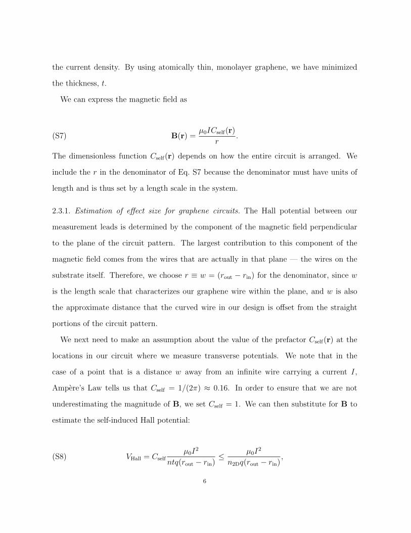
We can express the magnetic field as
(S7) B(r) =µ0ICself(r)
r.
The dimensionless function Cself(r) depends on how the entire circuit is arranged. We
include the r in the denominator of Eq. S7 because the denominator must have units of
length and is thus set by a length scale in the system.
2.3.1. Estimation of effect size for graphene circuits. The Hall potential between our
measurement leads is determined by the component of the magnetic field perpendicular
to the plane of the circuit pattern. The largest contribution to this component of the
magnetic field comes from the wires that are actually in that plane — the wires on the
substrate itself. Therefore, we choose r ≡ w = (rout − rin) for the denominator, since w
is the length scale that characterizes our graphene wire within the plane, and w is also
the approximate distance that the curved wire in our design is offset from the straight
portions of the circuit pattern.
We next need to make an assumption about the value of the prefactor Cself(r) at the
locations in our circuit where we measure transverse potentials. We note that in the
case of a point that is a distance w away from an infinite wire carrying a current I,
Ampere’s Law tells us that Cself = 1/(2π) ≈ 0.16. In order to ensure that we are not
underestimating the magnitude of B, we set Cself = 1. We can then substitute for B to
estimate the self-induced Hall potential:
(S8) VHall = Cselfµ0I
2
ntq(rout − rin)≤ µ0I
2
n2Dq(rout − rin),
6
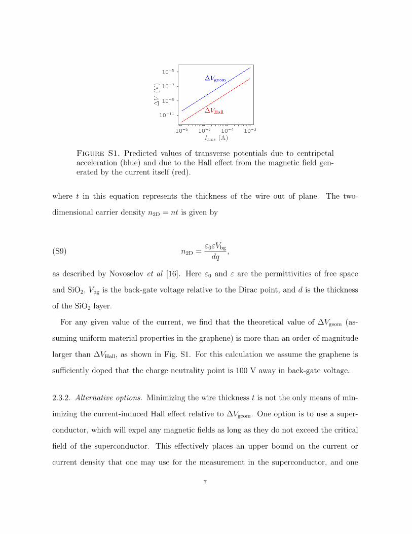
Figure S1. Predicted values of transverse potentials due to centripetalacceleration (blue) and due to the Hall effect from the magnetic field gen-erated by the current itself (red).
where t in this equation represents the thickness of the wire out of plane. The two-
dimensional carrier density n2D = nt is given by
(S9) n2D =ε0εVbgdq
,
as described by Novoselov et al [16]. Here ε0 and ε are the permittivities of free space
and SiO2, Vbg is the back-gate voltage relative to the Dirac point, and d is the thickness
of the SiO2 layer.
For any given value of the current, we find that the theoretical value of ∆Vgeom (as-
suming uniform material properties in the graphene) is more than an order of magnitude
larger than ∆VHall, as shown in Fig. S1. For this calculation we assume the graphene is
sufficiently doped that the charge neutrality point is 100 V away in back-gate voltage.
2.3.2. Alternative options. Minimizing the wire thickness t is not the only means of min-
imizing the current-induced Hall effect relative to ∆Vgeom. One option is to use a super-
conductor, which will expel any magnetic fields as long as they do not exceed the critical
field of the superconductor. This effectively places an upper bound on the current or
current density that one may use for the measurement in the superconductor, and one
7
must ensure that the noise floor of the lock-in amplifier does not exceed the expected size
of the signal ∆Vgeom when using that amount of current.
Another option is to intentionally design the circuit’s geometry to minimize the function
Cself(r) at the location of the curved wire, as a way to minimize ∆VHall in Eq. S8. One
way to accomplish this would be a two-layer circuit design. In the first layer, a thin,
flat wire follows a path through a curved section and a straight section, similar to the
graphene circuit design that we have used. At one end of the pattern, however, the wire
could instead connect to a second conducting layer, directly on top of the first, with a thin
insulating spacer, such that the wire then traces out an identical path but such that the
current will travel through the second layer in the opposite direction. The contribution
of both layers to the out-of-plane magnetic field would be minimized, for the same reason
that the magnetic field is minimized outside of a coaxial cable or a pair of twisted cables
that carries current in both directions.
8