a low power configurable soc for simulating delay … · a low power configurable soc for...
TRANSCRIPT
978-1-4673-2921-7/12/$31.00 c©2012 IEEE
A Low Power Configurable SoC for Simulating Delay-based Audio Effects
Ling Liu1, Jeremia Bar2, Felix Friedrich1, Jurg Gutknecht1
Computer Systems InstituteETH Zurich
Zurich, Switzerland1{ling.liu, felix.friedrich, gutknecht}@inf.ethz.ch, [email protected]
Shiao-Li Tsao3
Department of Computer ScienceNational Chiao Tung University
Hsinchu, [email protected]
Abstract—The rapid growth in the capability of modernFPGA devices allows developers to build a complete systemon a single chip. These types of FPGA-based SoC (System-On-a-Chip) can normally achieve reduced system power, costand size, and at the same time offer users a great dealof flexibility. The development of such SoCs normally startsfrom using a hardware / software co-design methodology inorder to partition system tasks into computation-intensive andflexibility-demanding parts. Then, dedicated hardware andsoftware will be implemented to realize these two parts. Thispaper presents an example which demonstrates the result ofapplying the hardware / software co-design methodology, apower efficient and performance reliable system architecturefor realizing audio delay effects. Compared to similar imple-mentations, our system architecture can save 40% of dynamicpower consumption while offering the same data throughputand user flexibility.
Keywords-low-power SoC, hardware / software co-design,FPGA, delay-based audio effects.
I. INTRODUCTION
In the field of music, delay-based audio effects simula-tion systems are widely used to create a sense of spacefor listeners. The algorithms for delay-based audio effectsand their realization techniques such as FIR(Finite ImpulseResponse), IIR(Infinite Impulse Response) filters, delay linesand periodical modulators have been studied extensively inthe last fifty years [1], [2], [3], [4], [5]. However, veryfew study results have been found in the entire systemarchitecture, especially with regard to effects on systempower consumption.
For a real-time audio effects simulation system, the per-formance requirement is that the system can produce outputsat a sampling rate. Apart from the performance requirement,it is normally expected that the system allows users toconfigure the effect parameters and route the audio streamduring the run time. The goal of our system architecturedesign is to meet these performance and programmabilityrequirements with low power consumption cost. To achievethis goal, hardware / software co-design methodology is usedin the system development process. The delay-based audioeffects SoC presented here is implemented on an FPGA chip.In the system, dedicated hardware is used to realize the audioeffects and route the audio stream. A tiny register machine
(TRM) soft-core processor and the software running on topof it are used to control the parameters of the audio effectsand the routing matrix. Compared to the existing studiesof audio effects SoC implementation [6], [7], the systemarchitecture presented here has the following characteristics.
• Instead of soft-core-centric design, this paper presentsa distributed on-chip system. That is, the data buffersrequired by the audio effects hardware are neithercontrolled by the soft-core nor accessed via the softwarerunning on the soft-core. They are implemented in thededicated hardware using BRAMs (Block RAMs) onan FPGA chip. This design reduces the possible perfor-mance unreliability caused by software and decouplesthe hardware from software to allow the hardwarecomponent to run at a much lower clock rate, in ourcase, 48KHz.
• Instead of 48MHz or an even higher clock rate, theaudio effects hardware in our SoC runs at a samplingrate of 48KHz. Therefore, our system can save 40%dynamic power according to estimation results.
• Instead of software, a switch matrix is implemented tocontrol the routing of the audio stream. Using dedicatedhardware to control the routing of the audio stream canavoid unpredictable delay caused by the software andallow hardware to run at a much lower clock rate.
• Instead of a fully fledged commercial soft-core, suchas MicroBlazer from Xilinx and NIOS from Altera, acustomized soft-core processor TRM is implemented onthe FGPA to minimize the resource and area cost. TheTRM implementation on a Virtex-5 FPGA only uses728 LUTs, while most commercial soft-core processorsrequire roughly 2000 LUTs or LEs. Therefore, theuse of a customized soft-core processor dramaticallyreduces the area cost of the entire system and, as aresult, also reduces the power consumption of the entiresystem.
The system architecture is presented in Section II. Thededicated hardware for delay-based audio effects and therouting matrix are introduced in Section III. The parametercontrol is described in Section IV. Section V presents thesystem evaluation results. Finally, we conclude this paper in

Figure 1. Block diagram of our delay-based audio effects SoC.
Section VI.
II. SYSTEM ARCHITECTURE
Figure 1 shows that our real-time delay-based audioeffects SoC is implemented on a Virtex-5LX50T chip, whichis used on our target platform - a Xilinx ML505 board. Theboard uses an AC’97 compatible audio codec with 48KHzsampling rate and 20-bit resolutions. Four delay-based audioeffects, i.e. chorus, flanger, reverberation and vibrato, arerealized in the system. These effects are implemented in thededicated hardware, and can send and receive a real-timeaudio-stream to / from a routing matrix to allow differentaudio effects to be dynamically combined. The audio effectshardware and the routing matrix receive a parameter streamfrom the FIFO (First In and Fist Out) connected to theTRM soft-core processor. The system architecture shown inFigure 1 can provide reliable performance, i.e. 48K samples/ second, as required by real-time audio effects with flexibleconfigurability.
To achieve the reliable performance and system flexibilitywith low-power consumption, the system implementation isdivided into two clock domains: a 25MHz clock domain anda 48KHz sampling clock domain. The 25MHz clock drivesthe TRM and a UART (Universal Asynchronous Receiverand Transmitter) controller. The 48KHz clock drives aparameter decoder, delay-based audio effects and the routingmatrix hardware to allow the system to produce outputsamples at the sampling rate. An asynchronous FIFO is usedto allow communication between these two clock domains.
The reliable performance of the system is ensured by thededicated hardware used to realize audio effects and routethe audio stream. The buffer memory required by the audioeffects is implemented using on-chip BRAMs. Therefore,there is no off-chip memory like SDRAM built in thesystem. In addition, the Xilinx ISE library provides variousinterfaces of BRAM macros. This allows us to cascade andcombine BRAMs to form different sizes of buffer memoryfor each effect. This buffer memory implementation avoidsmemory bottleneck and unreliable performance caused by aglobal buffer memory accessed via the software running ona soft-core processor. Together with the dedicated routingmatrix hardware, it finally decouples the software from thehardware and allows us to use different clock domains toachieve low-power consumption with ensured performance.
The system flexibility is achieved by the software runningon the soft-core processor TRM. The software receives effectparameters and routing commands via the UART to controlthe audio effects and the routing matrix during the runtime. According to a user’s requirements, a set of simplecommands or a complicated graphical application can bedeveloped on the user’s desktop or tablet PC. The PC-side application can send the effect parameters and routingcommands to the target system to allow users to adjustthe effects in real time. A wireless-to-UART adapter canalso be used to allow users to control the target systemin a more convenient way. If another user interface, forexample a MIDI controller, is preferred by end users, simplyreplacing the UART controller with another I/O controllerwill be sufficient. The performance critical data path willnot be affected at all. Therefore, this system architecturenot only allows end users to easily control the system, butalso allows developers to easily adapt the system to differentI/O interfaces.
The interface between the software and hardware is anasynchronous FIFO buffer. The TRM processor accesses thisFIFO buffer via memory mapped I/O. The simple interfacebetween the software and the hardware parts reduces thearea cost. As a result, it also reduces the system powerconsumption.
The low-power consumption of the system is mainlyachieved by the low clocking rate used in the dedicatedhardware. In our system, 74% (2302 LUTS out of a toal3100 LUTS) of the circuitry is used for the dedicated hard-ware. Considering that our dedicated hardware is runningat 48KHz, the dynamic power consumption of our systemis much less than the existing systems [6], [7]. In addition,the power consumption of our system is further reduced bynot using off-chip memory, the small footprint of the soft-core processor and the simple interface between the soft-coreprocessor and the dedicated hardware.
III. DEDICATED HARDWARE DESIGN
This section introduces the architecture and the config-urable interfaces of the hardware components in the audiostream data path. The hardware components and their organi-zation introduced here take advantage of the DSP support inmodern FPGA devices, such as multipliers, fast carry chainsand BRAMs, to reduce the resource and power costs of thesystem.
A. Basic Building Blocks
Delay-based digital audio effects are widely used inrecording studios and live musical events to create differ-ent interpretations of the sense of space and environment.This section presents the design and implementation of theconfigurable delay-based audio effects.
1) Delay Line: The delay line is an elementary functionalunit which models acoustic propagation delay. It is a funda-mental building block of both delay-effects processors anddigital-waveguide synthesis models. The function of a delayline is to introduce a time delay, corresponding to M samplesbetween its input and output [8].
Our configurable delay line implementation has an inputsignal, delaySize, to allow the configuration of the delaybuffer size at the run time. The number of cycles for thecircuitry to react to the new delay size configuration is|newDelaySize - oldDelaySize|, the difference between thenew delay size and the old delay size. During that time, asample value is interpolated into the audio stream. This delayline implementation can store a maximum of 5K samples.Because the sampling rate of AC’97 codec is 48KHz, thelongest delay that can be simulated by the delay line imple-mentation is (1s/48000) · 5120 = 106.7ms. According to[9], if the delay is in the range between 10 and 25 ms, a quickrepetition called “slapback“ or “doubling“ can be heard.If the delay is greater than 50ms, an echo will be heard.Therefore, this configurable delay line implementation cansimulate both of these effects according to the value of theinput signal delaySize.
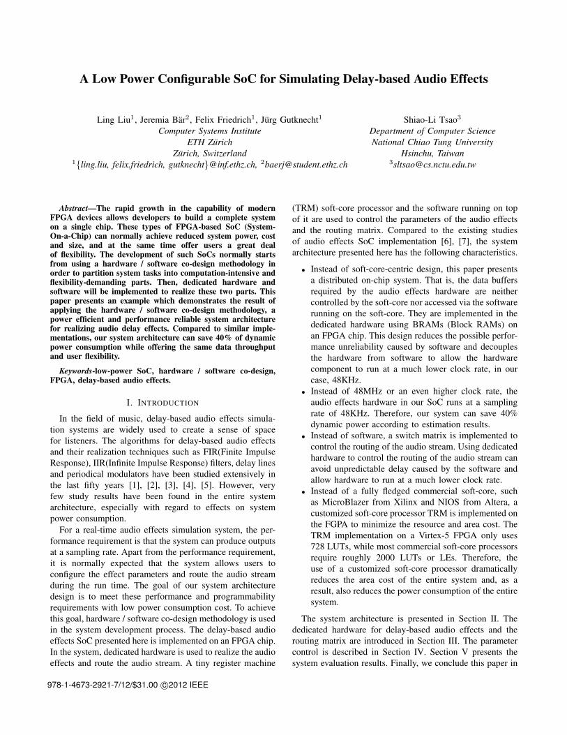
2) Comb Filter: Comb filters are used to simulate acous-tic echo effects. There are two basic comb-filter types:feedforward and feedback comb filters. The feedforwardcomb filter models a single discrete echo by inserting thedelay line into the feedforward path. The feedback combfilter models multiple echoes by inserting the delay lineinto the feedback loop. Figure 2 shows the schematic ofthe feedforward and feedback comb filters. The M samplesdelay in the schematic is implemented by the configurabledelay line introduced before. The delay size M and the gainof the comb filters are input signals and therefore can beconfigured at run time. The multiplication is implementedwith DSP slices on the FPGA chip, and uses fixed pointnumbers.
Figure 2. Block diagram of comb filters.
3) All-pass Filter: The feedback comb filter is the mainbuilding block for simulating reverberation effects. However,as Schroeder pointed out [10], the amplitude-frequencyresponse of the feedback comb filter has the appearance ofa comb with periodic maxima and minima. These periodicmaxima and minima impart the undesired ”colored” qual-ity to the reverberated sound. To eliminate the undesired”colored” quality and improve the echo density of thereverberation effect, Schroeder and Logan introduced all-pass filters, which have amplitude-frequency 1 for eachfrequency. In our system, a direct-form-II implementation[11] of an all-pass filter has been implemented.
B. Delay-based Audio Effects
1) Reverberation: Reverberation refers to the prolonga-tion of sound by the environment, which is essentiallycaused by the reflectivity of surfaces and by the slow speedof sound in air, only about 345m/s at room temperature[12]. The characteristics of natural reverberation include thereverberation time, the dependency of the reverberation timeand the frequency, the time gap between the direct soundand the reverberation and, finally, the echo density rate. Thereverberation time is the time for a sound to die away to-60dB, and is also called T60. Different audible frequencieshave different reverberation times. In a concert hall, forexample, a low frequency sound tends to fade away last.The time gap between the direct sound and reverberationgives the listener a different sensation of the space. Forexample, a delay less than 5ms creates a sensation of asmall space, while a delay greater than 50ms gives a distinctecho. When sound radiates from a source, it first reaches thelistener along a direct path, then some early reflected anddecayed signals reach the listener, and in the end signalsreflected several times arrive at the listener and give thesense of very dense echoes. Therefore, the density rate of theechoes in the reverberation should be high enough to emulatethis last stage of the sound traveling process. Normally, toobtain a flutter-free reverberation, that is with no distinctaudible echoes, there should be approximately 1000 echoesper second. To reflect these reverberation characteristics ina digital reverberator, Schroeder introduced a design thatcombines comb filters and all-pass filters. Figure 3 shows the

Figure 3. Block diagram of Schroeder reverberator.
Figure 4. Block diagram of time varing delay effects.
block diagram of the Schroeder reverberator implemented inour system.
The delay line size and the gain of each filter used inFigure 3 can be configured by users at the run time to reflectthe reverberation time of the environment.
2) Vibrato, Flanger and Chorus: Vibrato, flanger andchorus effects are all time-varying delay effects designed tothicken the sound via the manipulating of the frequencies ofthe sound over time. When the delay time between the outputsignal and the input signal varies periodically, a vibratoeffect is generated. To simulate the periodically varying timedelay, an LFO (low frequency oscillator) is used with adelay line to change its size periodically. When adding theperiodically delayed signal to the original signal, a flangereffect is created. The effect was developed in recordingstudios in the 1950s by lightly pressing the outer ’flange’ ofone of two synchronized tape machines alternately. When anumber of players perform in unison, the small changes inthe amplitudes and timing between each individual result inthe chorus effect. Figure 4 gives the block diagram of thesethree time varying delay effects. Different configurationsof the dry gain, wet gain, feedback gain and delay timegenerate different effects. Here, dry signal means the originalsignal and wet signal means the delayed signal. Table Ishows different configurations used to generate differentdelay effects.
C. Routing Matrix
The routing matrix used to route audio streams betweendifferent effects is implemented using a crossbar intercon-nect. The 5 inputs of the crossbar are connected to the output
Table ITYPICAL PARAMETERS FOR TIME VARYING DELAY EFFECTS.
Effect g1 g2 g3 LFO LFO LFOFrquency Amplitude Offset
Chorus 0-1 0-1 0 0.2-2Hz 0-5ms 15-25msFlanger 0-1 0-1 0 0.5-5Hz 0-7.5ms 0-15msVibrato 0 1 0 5-15Hz 0-2.5ms 0-2.5ms
audio stream of the AC’97 codec, the output of the choruseffect, the output of the flanger effect, the output of theSchroeder reverberator and the output of the Vibrato effectseparately. The 5 outputs of the crossbar are connected tothe input of chorus effect, input of flanger effect, input ofSchroeder reverberator, input of vibrato effect and the inputaudio stream to the AC’97 codec.
IV. DYNAMIC CONFIGURATION
The dynamic configuration of the system is achieved viathe software running on a general purpose soft-core proces-sor, a TRM. This section introduces the TRM architectureand the software design.
A. Tiny Register Machine (TRM)
The TRM was originally designed and implemented onVirtex-5 FPGA by Prof. Niklaus Wirth [13]. The instructionset architecture of TRM is designed to be small but powerfulenough to run a program written in a high level programminglanguage, in our case, Oberon[14]. To demonstrate that thisdesign goal is achievable, a multicore processor composed of12 TRMs and a bus-based interconnect was implemented ona Virtex-5LX50 FPGA [15]. TRM is a Harvard architecturewith an 18-bit, 2-address instruction set and 32-bit datapath.The 18-bit instruction encoding allows each memory unit inthe Virtex-5 FPGA BRAM slice to store two instructions,Therefore, the scarce memory resource can be fully used.It has 8 working registers and a program counter register(PC). Out of the 8 working registers, register R7 is usedin BL(BranchandLink) instruction to store the returnaddress. By default, a TRM processor is configured with 4Kinstruction memory and 2k data memory. The memory sizecan be configured to meet the programmers’ requirements.The 2-stage pipelined implementation of a TRM runs at116MHz, and takes 2% LUTs of the Virtex-5XC5VLX50TFPGA. The multiplication in the TRM takes 5 clock cycles.
B. Software Implementation
The software development for a graphically configurablesystem involved two parts: developing software runningon the TRM processor that controls the signal processingengines on the FPGA and developing a graphical softwarerunning on a host PC which is connected to the client viasome serial interface. The software running on the hostPC can be in principle developed using any off-the-shelftools and languages, such as C#, Java or Matlab. In our
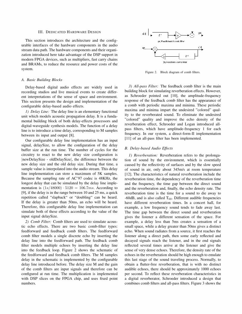
Figure 5. Configuration GUI running on the host PC.
case, Active Oberon is used to develop a graphical userinterface (GUI) application. This GUI application allowsusers to enter configuration parameters and send them tothe FPGA via the UART. Figure 5 shows a typical GUIscenario. The software running on the TRM reads the datasent from the host PC, computes the parameters requiredby the audio effect hardware and writes them into theasynchronous FIFO attached to the TRM and the parameterdecoder hardware. The software running on the TRM is alsowritten in Oberon because an Oberon compiler for the TRMhad been developed in our group [16]. There is no operatingsystem running on the TRM.
V. SYSTEM EVALUATION
Table II shows the resource usage of the entire system.Table III shows the power consumption results with re-gards to different system configurations. We consider threedifferent configurations: the proposed 25MHz(TRM)withthe 48KHz(Effects) design, and two soft-core-centric ap-proaches that use the same clock for soft-core and audioeffects. To the best of our knowledge, the clock used inthe existing systems [6], [7] to drive the soft-core and theeffects is equal to or more than 48MHz. Therefore, the25MHz(TRM) with the 25MHz(Effects) and 50MHz(TRM)with the 50MHz(Effects) system configurations listed in Ta-ble III are used to estimate the possible power consumptionin the similar systems. The power estimation results shownin Table III are generated by XPower[17]. The total powerconsumption of an FPGA system consists of static powerand dynamic power. The static power which can be derivedby VDDIleakage is decided by the leakage current (Ileakage)from the FPGA chipset with VDD supply voltage. As canbe seen from Table III, all three configurations consumethe same amount of leakage power. The improvement ofthe proposed solution, which optimizes clock domains forperformance-critical hardware components and highly flex-ible soft-core, comes from the reduction in dynamic power.The dynamic power can be modeled by ACVDD
2 f, whereA, C and f denote the activity factor, the capacitance factor ofthe FPGA, and the operating clock frequency, respectively.Although the total power consumption of the system is onlyreduced by 6.5%-13.3% by applying the proposed design
Table IIRESOURCE USAGE OF THE SYSTEM ON VIRTEX-5LX50T CHIP.
LUTs BRAMs DSPs
3100 (10%) 48 (80%) 15 (31%)
idea, we expect that the improvement can increase whenmore FPGA resources are utilized, because currently only10% LUTs are used in our system. Reports indicate thatdynamic power still dominates the total power consumptionof FPGAs and it takes 60%-80% of the total power for thelatest 28-nm FPGA [18], [19] assuming the resources arefully used.
Dynamic power includes the dynamic power of soft-core,i.e. TRM, audio effect hardware components, and compo-nents such as clock managers and I/O terminations, whichare default components in all FPGA designs[20]. Since soft-core and default components are the same for all threecases, the dynamic power reduction comes from reducing theclock rates of audio effect hardware components. Table IIIreveals that the proposed design concept can reduce dynamicpower by 22.9%-39.6% compared with the existing soft-core-centric solutions. After examining the details of theimprovement, we find that the power consumption of IOsand PLLs remains unchanged for all three designs. Thisis because three designs use the same I/Os and the samePLLs which generate the global clocks for the FPGA. DSPis energy efficient and its power consumption is almost neg-ligible in this case study. Clocks and logic reduce dynamicpower consumption by 11.5%-27.3% and 26.1%-63.0%compared with soft-core-centric solutions. The improvementis not proportional to the clock frequency since the clockand logic blocks are mainly consumed by the TRM anddefault components. The dynamic power of signal blocksand block memory (BRAMs) is considerably reduced. Thetwo components are mainly used in audio effect hardwarecomponents and can reduce dynamic power significantlyby slowing down the clock frequencies from 50MHz and25MHz to 48KHz. Our experimental measurement of powerconsumption on the prototype system using a multimetershows a 25%-30% improvement and matches the estimationresults produced by XPower.
VI. CONCLUSION
The low-power audio effect system presented here givesan example of a heterogeneous architecture for FPGA-based SoCs. The software / hardware partitioning and theuser interface of this system show that it can offer thesame flexibility as the pure software-based implementation.The clock domain partitioning and the dedicated hardwareimplementation provide the reliable performance required bya real-time SoC. More importantly, the power consumptionestimation results show that this heterogeneous architectureis very power efficient.
Table IIICOMPARISONS OF POWER CONSUMPTION FOR DIFFERENT SYSTEM
CONFIGURATIONS.
Power consumption item 25MHz(TRM) 25MHz(TRM) 50MHz(TRM)(unit: mW) 48KHz(Effects) 25MHz(Effects) 50MHz(Effects)
Total power 577.78 617.81 666.08(6.5%)∗ (13.3%)∗
Leakage power 444.15 444.43 444.77
Dynamic power
Total 133.63 173.38 221.31(22.9%)∗ (39.6%)∗
Clocks 36.04 40.71 49.55(11.5%)∗ (27.3%)∗
Logic 0.17 0.23 0.46(26.1%)∗ (63.0%)∗
Signals 0.62 2.26 4.24(72.6%)∗ (85.4%)∗
IOs 6.91 6.91 6.91(0%)∗ (0%)∗
BRAMs 3.29 36.72 73.45(91.0%)∗ (95.5%)∗
DSPs 0.07 0.07 0.14(0%)∗ (50%)∗
PLLs 86.52 86.48 86.56(0%)∗ (0%)∗
∗% power saving compared with the proposed 25MHz(TRM), 48KHz(Effects) design.
ACKNOWLEDGMENT
A substantial part of the work is the result of the project‘Supercomputer in the Pocket’. We thank the MicrosoftInnovation Cluster for Embedded Software for funding thisproject. The authors would also like to thank ProfessorNiklaus Wirth for his work with TRM processor design.
REFERENCES
[1] Z. Smekal, J. Schimmel, and P. Krkavec, “Optimizing digitalmusical effect implementation for harvard dsp architecture,”in Proceedings of the COST G-6 Conference on Digital AudioEffects, ser. DAFx-01, Limerick, Ireland, 2001, pp. 33–38.
[2] T. Choi, Y.-C. Park, and D. H. Youn, “Design of time-varying reverberators for low memory applications,” IEICETransactions, vol. 91-D, no. 2, pp. 379–382, 2008.
[3] F. P. Ling, F. K. Khuen, and D. Radhakrishnan, “An audioprocessor card for special sound effects,” in Proceedings ofthe 43rd IEEE Midwest Symposium on Circuits and Systems,Lansing MI, 2000, pp. 730–733.
[4] J. Dattorro, “Effect design: Part 1: Reverberator and otherfilters,” Journal of Audio Engineering Society, vol. 45, no. 9,pp. 660–684, 1997.
[5] N. Juillerat, S. Schubiger-Banz, and S. M. Arisona, “Lowlatency audio pitch shifting in the time domain,” in Proceed-ings of the 43rd IEEE Midwest Symposium on Circuits andSystems, ser. ICALIP 2008, Shanghai, China, 2008, pp. 29–35.
[6] M. Pfaff, D. Malzner, J. Seifert, J. Traxler, H. Weber, andG. Wiendl, “Implementing digital audio effects using a hard-ware/software co-deisgn approach,” in Proceedings of the10th International Conference on Digital Audio Effects, ser.DAFx-07, Bordeaux, France, 2007, pp. 125–132.
[7] R. Trausmuth, C. Dusek, and Y. Orlarey, “Using faust forfpga programming,” in Proceedings of the 9th InternationalConference on Digital Audio Effects, ser. DAFx-06, Montreal,Canada, 2006, pp. 287–290.
[8] J. O. S. III, Physical Audio Signal Processing. Stanford Uni-versity: Julius O. Smith III, W3K Publishing, 2010, availableelectronically from: https://ccrma.stanford.edu/ jos/pasp/.
[9] U. Zolzer, X. Amatriain, D. Arfib, J. Bonada, G. D.Poli, P. Dutilleux, G. Evangelista, F. Keiler, A. Loscos,D. Rocchesso, M. Sandler, X. Serra, and T. Todoroff, Eds.,DAFX:Digital Audio Effects, 1st ed. The Atrium, SouthernGate, Chichester West Sussex PO19 8SQ, England: JohnWiley Sons, Ltd, 2002.
[10] M. R. Schroeder, “Natural sounding artificial reverberation,”Journal of the Audio Engineering Society, vol. 10, no. 3, pp.219–223, 1962.
[11] J. O. S. III, Introduction to Digital Filters with Au-dio Applications. Stanford University: Julius O. SmithIII, W3K Publishing, 2007, available electronically from:https://ccrma.stanford.edu/ jos/filters/.
[12] V. Valimaki, J. D. Parker, L. Savioja, J. O. Smith, and J. S.Abel, “Fifty years of artificial reverberation,” IEEE Trans-actions on Audio, Speech & Language Processing, vol. 20,no. 5, pp. 1421–1448, 2012.
[13] N. Wirth, “The Tiny Register Machine (TRM),” ETH Zurich,Computer Systems Institute, Tech. Rep. 643, 10 2009.
[14] N. Wirth and J. Gutknecht, Project Oberon : the design of anoperating system and compiler. New York etc.: ACM Press,1992.
[15] L. Liu, “A 12-core processor implementation on FPGA,” ETHZurich, Computer Systems Institute, Tech. Rep. 646, 10 2009.
[16] F. Friedrich, L. Liu, and J. Gutknecht, “Active cells: Acomputing model for rapid construction of on-chip multi-coresystems,” in ACIS-ICIS, 2012, pp. 463–469.
[17] Xilinx, “Xpower,” http://www.xilinx.com/products/design tools/logic design/verification/xpower.htm.
[18] J. Hussein, M. Klein, and M. Hart, “Loweringpower at 28 nm with xilinx 7 series fpgas,”http://www.xilinx.com/support/documentation/white papers/wp389 Lowering Power at 28nm.pdf.
[19] Altera, “Reducing power consumption andincreasing bandwidth on 28-nm fpgas,”http://www.altera.com/literature/wp/wp-01148-stxv-power-consumption.pdf.
[20] Xilinx, “Xpower estimator user guide,”http://www.xilinx.com/support/documentation/user guides/ug440.pdf.