a linear array design based on non-uniform chebyshev
TRANSCRIPT

A linear array design based on non-uniform Chebyshev
distribution for high gain low sidelobe level millimetre
wave 5G applications.
A Master's Thesis
Submitted to the Faculty of the
Escola Tècnica d'Enginyeria de Telecomunicació de Barcelona
Universitat Politècnica de Catalunya
by
Shaheen Ahmad
In partial fulfilment
of the requirements for the degree of
MASTER IN TELECOMMUNICATIONS ENGINEERING
Advisors: Prof.Rashid Mirzavand, Dr.Mohammad Mahdi Honari, Prof.Lluis Jofre
Edmonton Canada, July 2020

1

2
Title of the thesis: A linear array design based on non-uniform Chebyshev
distribution for high gain low sidelobe level millimetre wave 5G applications
Author: Shaheen Ahmad
Advisor: Prof.Rashid Mirzavand, Dr.Mohammad Mahdi Honari, Prof.Lluis Jofre.
Abstract
Antenna is the front-end element and is a major part of designing a robust communication system.
The increased user density and high data rate requirements now a days can be overcome by a
wideband antennas capable of having a stable radiation pattern with high gain and low sidelobe level.
This study presents the design and analysis of a linear array antenna based on Chebyshev current
distribution for mm-wave applications. An extensive review of the most recently published work on
array design and architecture for the future generation (5G) antennas is also included. Systematic
approach is followed towards the design of eight elements corporate feed for non-uniform amplitude
excitation using unequal power split T-junctions. The array is designed on a Rogers RO5880tm
substrate with a compact size of 45 x 15 x 0.32 mm3. Two design configurations have been
demonstrated. The simulation results show that the first design offers an impedance bandwidth of 5%
and a gain and sidelobe level (SLL) of 12 dB and -16 dB, respectively. To further enhance the antenna
array performance a second array design is proposed. The modified design has an improved
impedance bandwidth of 13%, also the gain and SLL have been enhanced to 14 dB and -19 dB,
respectively. Results of the first array configuration have been validated by fabricating and testing the
antenna prototype. The proposed array antenna is a promising candidate for the future mm-wave
communication devices due to its compact structure and very good performance parameters such as
high gain, wide-bandwidth and reduced sidelobe level.
Index Terms- Antenna array, millimeter wave, 5G, bandwidth, Beamforming, efficiency, gain,
architecture, antenna pattern, broadband, reconfigurability. Antenna array feed, side lobe level,
optimization, narrow beam, tapered array.

3
Revision history and approval record
Revision Date Purpose
0 05/06/2020 Document creation
1 11/08/2020 Document revision
2 21/08/2020 Document revision
Written by: Reviewed and approved by:
Date 05/07/2020 Date 31/August/2020
Name Shaheen Ahmad Name Prof.Rashid Mirzavand
Position Project Author Position Project Supervisor

4
Table of contents
Abstract .......................................................................................................................... 2
Revision history and approval record .......................................................................... 3
Table of contents ........................................................................................................... 4
List of Figures ................................................................................................................ 5
List of Tables ................................................................................................................. 8
1. Introduction ............................................................................................................. 9
1.1. Motivation of research ……………………………………………...…………….……9
1.2. Contribution and organization of the dissertation ………………………………….11
2. Array antenna background and principles ........................................................ .12
3. Array antenna classification …...…………………………………………………..….13
3.1. Beamforming array design and techniques ……………………...……….............13
3.2. Multibeam arrays ……………………………………………………….…..…….….16
3.3. Retrodirective antenna arrays ………………………………………….….…….….18
3.4. Active antenna arrays ………………………………………………….……….…...20
3.5. High gain antenna arrays …………...………………………………….…..……….22
3.6. Antenna arrays with low sidelobe level ………………………….…………..….….24
4. Array antenna design based on Dolph-Tschebyshev distribution .................... 28
4.1. Single element antenna design ………………………………………………….….29
4.2. Chebyshev feed network design ………………………………...………………….33
4.3. Array antenna design ………………………………………………………..………35
4.3.1. First array design configuration ………………………………………………..36
4.3.2. Second array design configuration ……………………………………………37

5
5. Results .................................................................................................................. 37
5.1. Simulation results of the first design configuration …………………………….....38
5.1.1.1. Return loss ……………………………………………………….…...………38
5.1.1.2. Radiation pattern …………………………….…………..……………….…39
5.1.1.3. Surface current plots ……..…………………………………………………41
5.1.2. HFSS results of the first array design ……………………………….….…42
5.2. Simulation results of the second design configuration ………….………….….…45
5.2.1.1. Return Loss ……………..…………………………………………….....…..45
5.2.1.2. Radiation Pattern ………..……………………………………………..……46
5.2.1.3. Surface current plots ……..……………………………………………..…..47
5.2.2. HFSS results of the second array design ………….…………………..…47
6. Fabrication and Testing …………………………………………….……………..…….50
6.1. Measured reflection coefficient results……………………….……………………..50
7. Budget ………………………………………………………………………..………...….52
9. Conclusions and future development ................................................................. 52
Bibliography ................................................................................................................ 54
Glossary ....................................................................................................................... 62

6
List of Figures
Figure 1.1 SICL fed array antenna design geometry and results ............................................. 12
Figure 2.1 Figure 2. Array of ‘r’ elements separated by equal distance along z-axis ................. 13
Figure 3.1 Geometry and results of beamformer antenna ....................................................... 14
Figure 3.2 Differential views of the 3-subarray antenna ........................................................... 15
Figure 3.3 Geometry and results of the series fed array antenna ............................................. 16
Figure 3.4 Waveguide lens array antenna geometry and results .............................................. 17
Figure 3.5 Multibeam reflect array antenna geometry and results ........................................... 18
Figure 3.6 Retrodirective array antenna .................................................................................. 19
Figure 3.7 Circular retrodirective array with the radiation pattern results .................................. 19
Figure 3.8 Geometry and results of the active array antenna .................................................. 21
Figure 3.9 Subarray active antenna geometry and radiation pattern ........................................ 21
Figure 3.10 Geometry of the beam steerable high gain array antenna ....................................... 23
Figure 3.11 Cavity antenna design and radiation pattern results ............................................... 23
Figure 3.12 Array antenna with feed network geometry and results ........................................... 25
Figure 3.13 Geometry of the SIW antenna and fabricated prototype .......................................... 26
Figure 4.1 Geometry of the proposed single element antenna ................................................ 30
Figure 4.2 Return loss of the poroposed single element antenna ............................................ 31
Figure 4.3 Surface current plots of the proposed single element antenna ................................ 31
Figure 4.4 2D Radiation pattern of the single element antenna ............................................... 32
Figure 4.5 Polar plots of the proposed single element antenna ............................................... 32
Figure 4.6 3D radiation plots of the single element antenna .................................................... 33
Figure 4.7 Proposed Chebyshev feed network ....................................................................... 34
Figure 4.8 Simulated amplitudes of all the eight ports ............................................................. 35
Figure 4.9 Simulated phases for all the ports .......................................................................... 35
Figure 4.10 Geometry of the first array design configuration ..................................................... 36
Figure 4.11 Geometry of the second array design configuration ................................................ 37
Figure 5.1 Reflection coefficient of the proposed first array design .......................................... 38

7
Figure 5.2 Smith chart representation of the proposed antenna impedance ........................... 38
Figure 5.3 Different views of the 3D radiation plots at 28 GHz ............................................... 39
Figure 5.4 Cartesian plots for far-field Gain radiation pattern ................................................. 40
Figure 5.5 Polar radiation plot of the first design at 28 GHz .................................................... 41
Figure 5.6 Surface current distribution of the proposed single layer antenna .......................... 41
Figure 5.7 2D Gain radiation pattern of the single layer antenna ............................................ 42
Figure 5.8 HFSS design of the first configuration array antenna ............................................. 42
Figure 5.9 Return loss of the proposed array antenna ........................................................... 43
Figure 5.10 Far-field cartesian gain radiation plot at 𝛟 = 𝟎𝟎 ..................................................... 43
Figure 5.11 Far-field Cartesian gain radiation plot at 𝛟 = 𝟗𝟎𝟎 .................................................. 44
Figure 5.12 2D polar gain radiation plot at 28 GHz ................................................................... 44
Figure 5.13 3D radiation plots of the proposed array at 28 GHz ............................................... 45
Figure 5.14 Reflection coefficient of the second antenna array ................................................ 45
Figure 5.15 Different views of 3D radiation plots at 28 GHz for the second design ................... 46
Figure 5.16 Far-field cartesian gain radiation plots of the second antenna array ...................... 47
Figure 5.17 Surface current distribution plots of the second design antenna ............................ 47
Figure 5.18 Geometry of the second array antenna configuration in HFSS .............................. 48
Figure 5.19 Return loss of the second design simulated in HFSS ............................................ 48
Figure 5.20 Far-field Cartesian gain radiation plot at 𝛟 = 𝟗𝟎𝟎 .................................................. 49
Figure 5.21 3D gain radiation plots of the second design in HFSS ........................................... 49
Figure 6.1 Prototype of the proposed first configuration array antenna .................................... 50
Figure 6.2 Measurement system for the return loss of the proposed antenna ......................... 51
Figure 6.3 Comparison graph of the simulated and measured return loss .............................. 51

8
List of Tables
Table 3.1 Comparison of the performance parameters of mm-wave antennas .................. 27
Table 4.1 Overall dimensions of the single element antenna ............................................ 31
Table 4.2 Theoretical and proposed current amplitudes for SLL=-25 dB ........................... 34

9
1. Introduction
1.1. Motivation of research
The emergence of new communication technologies almost every decade impacts our lives up to a
greater extent by offering a more connected world; but at the same time, it forges new challenges and
design constraints for the antenna terminal designers. Due to an increase in the number of connected
wireless nodes, the demand for data traffic and interference free communication has been increased
to fulfil the next generation communication requirements. Millimeter wave spectrum is one promising
solution to fulfil the bandwidth shortage for high-quality, low latency data communication [1]. The world
telecommunications conference (WRC-15) allocated several frequency bands for the next generation
5G networks in both the lower and millimeter wave frequency bands [2][3]. However, millimeter waves
are short range and very prone to be affected greatly by the propagation losses due to its small
wavelength [4]. According to Friis formula the propagation losses for millimeter waves increases much
more rapidly with the distance for both the line of sight (LOS) and non-line of sight (N-LOS)
communications. mm-Waves are also affected by the atmospheric conditions and can be severely
attenuated due to bad weather. These limitations can be overcome by designing directive antennas
with high gain and stable radiation patterns to be used in a dense network at ultra-high throughputs.
Highly directive Array antennas are used to increase the range and compensate for the losses of high
frequency bands used for the future generation networks. Direction of the main beam can be
controlled in a beam switchable array antenna by a mechanical or electronic means [5]. Both digital
and analogue beam shifters are used depends on the link scenarios. Beam steering combined with
phased array and MIMO antennas can provide efficient antenna performance and agility, but on the
other hand, they require an additional beam-forming network (BFN) that further increases the
complexity and cost of the overall systems. Also, the optimum results can be achieved using many
iterative techniques and very careful array synthesis [6]. Beam steering is also used with reflect arrays
to form a hybrid class of antennas, that offers small size, low cost, and improved gain performance
along with beam-forming capability. The paper presented in [7], is a reconfigurable reflect array
antenna based on liquid crystal technology. The proposed design has two reflectors, the
reconfigurability is achieved by the upper reflector using a liquid crystal mixture. The antenna offers
a gain of 25.1 dB with the beam steering functionality. These antennas reduce the complexity and
cost of a high gain array antenna up to a greater extent.
Another very popular way of compensating the high propagation losses of the millimetre waves is by
designing efficient array antennas through the use of proper feeding structure. Efficient feeding

10
provides characteristics such as wide bandwidth, high isolation, compactness and low cross
polarization for array antennas. Substrate integrated waveguide (SIW) is one popular way of feeding
high gain slot array antennas that provide simple, low profile feeding structure which can also be
easily integrated with other planar structures. SIW feeding is also used with various arrays antennas
to obtain a desired radiation pattern [8]. By considering the internal and external losses and proper
matching a synthesized radiation pattern with the specific characteristics can be obtained. High gain
antennas such as slot arrays can also be fed with a Series Coplanar Waveguide feed networks (CPW)
providing dual polarization, high port isolation and a single layer structure [9]. Some research also
suggests integration of high gain slot arrays with MIMO [10] for multi-functional antenna
characteristics. Substrate integrated coaxial line (SICL) feeding is another technique used for linearly
polarized high gain arrays [11]. Two substrate layers are used with the feeding network sandwiched
between them. For impedance matching Vias are used at each radiating element connecting the
ground and the inner conductor, as illustrated in Figure 1. The sidelobe level (SLL) is supressed to -
18dB by designing amplitude-tapering SICL power dividers and properly matched feed network. High
gain slot arrays are also widely used for base station applications due to its polarization diversity and
wide bandwidth. A dual polarized planar microstrip fed based on stepped impedance (SI) slots have
been proposed for wideband base station applications [12][13]. Both arrays follow the same design
procedure for different frequency bands. Different sizes of the SI slots and dual feeding help achieving
wideband dual polarization antenna characteristics. The proposed designs offer port isolation greater
than 30dB along with single stable radiation gain pattern.
The increase in number of heterogenous networks due to the next generation (5G) will massively
increase the cell density. Network densification will also affect the cell size, average power, and
decoupling of both uplink and downlink. Not only the bandwidth but also radiation pattern, gain
efficiency and polarization diversity need to be optimized. Array antennas with large electrical aperture,
wide bandwidth and narrow beam-width are well suited for future wireless links [14]. Large arrays are
used to mitigate the propagation and thermal losses and to keep a high gain with less dependence of
frequency by employing a constant antenna aperture. Phased arrays are one possible solution for the
future radar and satellite communications, providing high gain narrow beam characteristics [15], but
on the other hand phased arrays are complex to design and are lacking efficiency at millimeter waves.
An ultra-wideband (UWB) operation has been obtained by using tapered slots with phased arrays
[16,17]; however, these arrays have the limitation of complex structure and scan blindness issues.
Tightly coupled elements are also used with the limitation of beam width due to the mutual coupling
of array elements [18]. Some of these challenges can be catered by designing an optically fed tightly
coupled arrays (TCA). These antennas use a coherent optical feed to control analogue amplitude and

11
phase [19,20], and provide relatively high bandwidth, greater scanning angle, light weight, and low-
profile structure.
Most of the high gain directional beamforming array antennas have a narrow-beam that provides a
limited spatial coverage, making them inadequate for a multiuser communication. Therefore, an
extensive study has been done by researchers on multibeam antennas (MBAs) as an alternative of
beamforming array antennas. The MBAs are capable of generating independent high directive beams
to cover a pre-determined range [21]. MBAs used with MIMO antennas allows higher gain with good
spatial channel information and uncorrelated multipath propagation [22]. MBAs can also be used with
phased array antennas called Multibeam phased array antennas (MBPAAs), that utilizes analogue
RF, IF and BB phase shifting techniques to integrate and employ beamforming capability. Multibeam
antennas are however very expensive with high profile structures and are mostly used in radar and
satellite technologies.
1.2. Contribution and organization of the dissertation
This dissertation reviews the design and development of array antennas for the next generation
communication technologies (5G). An array antenna is designed based on chebyshev amplitude
distribution for mm-wave communication devices. The antenna design is realized using a corporate
feed for non-uniform amplitude excitation to feed the array elements. The designed antenna is
fabricated for the proof of concept and to compare the simulated and measured results.
Section 1 of the thesis presents various challenges related to mm-waves propagation along with the
requirements for the next generation 5G networks and some proposed array antennas. In section 2,
the background history and working principles of the array antenna from conventional arrays to the
recently designed modern array antennas is outlined. Array categorization based on design
methodology and working principle is discussed in section 3. Array antennas are classified on the
bases of their feeding techniques, types of radiating elements, radiation pattern and other
performance parameters. An extensive survey of various types of array antenna development and
classification over the last decade has been included. The study outlines the design, architecture, and
challenges of modern array antennas along with the insights into their anticipated use in the future
high data rate communication links. This part brings together all the major classes of antenna arrays
that could be potentially the key components for the next generation communication devices.
Section 4 presents the design and architecture of the two proposed Chebyshev array antennas. The
design configuration of a single element antenna is first presented, followed by the Chebyshev feed
network design. Two different arrays have been proposed by combing the feed network and by

12
replicating the single element antenna. The simulation results for the first design and the improved
second array antenna is outlined in section 5. The proposed designs have been analyzed both in CST
and HFSS and the obtained results are categorized separately in each subsection. Section 6 includes
the fabrication and testing of the first design configuration. Both the return loss and radiation
parameter have been tested and compared with the simulation results. A short summary of the project
expenses is outlined in section 7. Finally, section 8 provides concluding remarks and future work on
the dissertation.
Figure 1.1. (a) Proposed slot array antenna (b) 1-D layer architecture (c) Radiation pattern in yoz-plane.
(redrawn from [11]).
2. Array background and principles
The array technology of today is a result of over a hundred years of antenna evolution. The first ever
array antenna was designed by Guglielmo Marconi in 1901 for his transatlantic wireless
communication experiment. After his invention, during the next few decades including the Era of world
war II, the array antennas were refined in several revisions for communication radars and radio
astronomy. During this period a Yagi-Uda array with an end-fire radiation pattern was discovered by
H.Yagi and S.Uda [23], by using several directors and reflectors along with a single feed-point.
Phased arrays were also discovered during this period, although these antennas were fixed and very
large in size with limited frequency scan in both azimuth and elevation directions. Beam-steering is
also employed with phased arrays using mechanical means only. These arrays, however, had very
high cost which is the reason they were only limited to military use [24]. The beamforming technology
in phased arrays became more predominant after 1950s, most of the fully electronic devices long with
the phase shifters and digital processing techniques were developed. And after that the age of

13
semiconductors has been started, that revolutionized the antenna design industry along with many
others.
Antenna array is a combination of several identical elements separated by a particular inter-element
distance. By arranging these elements in a particular manner, the antenna gain, radiation pattern and
scan angle can be controlled. The increase in gain is a result of concentration of the radiation power
in a specific direction and also due to the reduction of beam-width as compared to a single element
antenna. Figure 2.1. Shows an array of ‘r’ elements distributed along z-axis and separated by an
equal distance ‘d’. The electric field radiated by these
elements can be represented by a simple mathematical
equation given by (1) [25].
𝑬 = 𝑪𝒆−𝒋𝒌𝒓
𝑨∑ 𝒂𝒑𝒇𝒑
𝑷𝒑=𝟏 (𝜽)𝒆𝒋(𝒑−𝟏)(𝒌𝒅𝒄𝒐𝒔𝜽+𝜷) ……… (1)
Where p is the integer, ap is the weight of the 𝑝𝑡ℎ radiator
element, 𝜃 and 𝛽 are the polar coordinate angles, C is a
constant and 𝑓𝑝 (𝜃) is the electric field of the 𝑝𝑡ℎ radiator.
The above equation is true for the same radiators
equidistantly separated by a distance ‘d’ and excited by
an equal amount of power.
Figure 2.1. Array of ‘r’ elements separated by equal distance along z-axis.
3. Array antenna classification
Antenna arrays are used for a variety of applications to improve the overall performance of the system.
Especially for the next generation of mobile communication, array antenna will be the core technology
for every front-end transceiver system. Every application has different requirements which need a
unique class of antenna. Mainly array antennas can be classified by the type of radiation pattern and
the radiating elements used. Most of the modern-day antennas provides wide area coverage, better
signal quality, high efficiency, beam-steering capability and reduced co-channel interference. From
the literature some widely used array antenna types and their optimization techniques will be covered
in the subsequent paragraphs.
3.1. Beamforming array design and techniques
Beam scanning is a vital technology since the early ages of antenna use. Most of the satellites, radars
and deep space communication need a beamforming antenna array for their operation. Old

14
Conventional antennas, however, used mechanical beam-steering with the aperture and reflector type
antennas. Bell laboratories designed a radar antenna for a scan angle of ±150 in the azimuth direction,
which was published by Friis and Lewis in 1947 [26]. This radar antenna was based on a rotary phase
shifter used for electromechanical phase shifting, developed in the 1940s [27]. Later on, electronic
phase shifting became a popular way to realize a wide angle beam- steering. Since then, digital and
analog beam forming became a popular way of designing beam steerable antennas.
In order to realize beam-steering capability a wide range of antenna structures have been proposed
for various frequency bands. Beam steerable phased array antennas (PAAs) at cm-/mm-wave
frequencies have gained much attention of the researchers in both the industries and academia.
Phased array analog beam combiners are used for phase shifting and transmission length adjustment
to realize beamforming characteristics. The typical scan angle of most of the beamforming single
array is around 600. Therefore, some authors proposed using several subarrays in a small size
communication device to get a wide-angle coverage [28]. Two phased arrays, each composed of
eight identical cavity backed slot elements are capable to offer a high gain fan-beam radiation
coverage with a ±600 beam angle scanning as shown in Figure 3. This design also has a negligible
feeding structure insertion loss of 1 dB that has almost no effect on beam squint of the proposed
antenna array. The beam-steering is realized by the use of eight 6 b local oscillator phase shifter
within the RFIC chip.
(a) (b) (c)
Figure 3.1. (a) Different views of the proposed mobile device. (b) simulated radiation pattern of one subarray for
different beam scanning angles. (c) 2D radiation pattern of a single array for several scanning angles.(Redrawn from
[24]).
The use of more than two subarrays in a single device has also been studied for extended scan angle
coverage. For instance, 3 subarrays are incorporated in a cell phone device to achieve a 3D coverage
by selecting the desired subarray through the use of switching circuit [29]. Each of the subarray

15
covers around ±900 of the space, although their radiation pattern partially overlaps each other as
shown in Figure 4. The proposed phased array antenna can cover at least half of the space, therefore
in order to cover the whole space, a second antenna with the same 3 subarrays can be used on the
other side of the cell phone.
Analog beamforming phased array antennas based on optical up-conversion of RF signals for analog
spatial beamforming is also one popular solution for high gain, high data rate requirements [30]-[32].
Upconverting the transmitted and received signal maintain the spatial coherence throughout the array.
These designs provide an agile beam along with the minimization of non-linearities in array antennas.
Compact steerable phased array antennas are also designed for mobile phone applications, by using
switching techniques instead of phase shifters that reduces the overall size to fit in a small volume
[33,34]. Switching can help excite different parasitic elements loaded with different reactive
impedances, and help steering the radiation pattern in the desired direction. However, such designs
entail with the switching loss which is an important design factor that needs to be considered. Despite
the advantages of phased array antennas , there are some serious drawbacks that limit its use in
some electronic devices. The reduction of effective apertures of planar phased array antenna by the
cosine of the scan angle offers a low gain at large scan angle, which reduces the overall scanning
angle. The use of phase shifters and other bulky components increase the overall array antenna size
and make them more expensive for the publicly used consumer portable devices.
(a) (b) (c)
Figure 3.2. (a) Different views of the 3 subarrays. (b) Gain pattern of a single subarray for several scanning angles
simulated. (c) 3D radiation pattern of all subarrays for different beam scanning angles. (Redrawn from [29]).
To address some or all the above-mentioned limitations of phased array antennas, some authors
suggest use of lens antennas for proper beam-steering. The lens antenna in [35] is designed on a
low-temperature co-fired ceramics (LTCC) technology This planar lens antenna provides a full 2-D
beam scanning at high gain. The design is based on six rings each with a different relative permittivity

16
value. These different dielectric values produce the desired phase delay necessary for obtaining a
tilted beam in the required direction [36]. An orthogonality fed based patch array antenna also provide
a high degree 1-D beamforming agility [37]. The design of Figure 5 is composed of a series fed simple
microstrip and transformers adjusted at every element for better results and dual polarization which
makes the design very compact and simple to fabricate. For the realization of beamforming several
antenna array columns must be arranged as an array. Dual polarization usually need an aperture
coupled feed structure which is very difficult to fabricate, however the current design combines both
the simplicity of series feeding and dual polarization in a single antenna array.
(a) (b) (c)
Figure 3.3. (a) Front view of the antenna array (b)Geometry of a single element (c)Measured and simulated antenna
radiation pattern. (Redrawn from [37]).
3.2. Multi-beam arrays
The next generation communication is based on a multi-user mobile communication for improved data
rate, throughput and efficiency. Multi-beam antennas are used to cover multiple users simultaneously
at a time by generating several independent high gain directional beams. These antennas also exhibit
least design complexity and minimum physical size as compared to other high gain narrow beam
antenna arrays [38]. Owing to its importance in the future communication network architecture,
researcher have put a lot of effort in designing various multi-beam antennas. Multi-beam phased array
antennas using rotman lens has been the focus for several years. A 2-D array can be designed with
multi-beams for near-field focus (NFF) applications [39]. By feeding the lens at three different points,
an individual directive beams can be generated in three different directions. The rotman lens antenna
can be extended to an efficient beamforming multibeam array antenna by using a beam forming
network referred as NFF rotman lens beamformer. Beamforming network used in multibeam antennas
is an alternative of smart antennas using beam scanning based on division multiple access to scan
the target zones. The concept of 2-D rotman multibeam antenna can be extended to a 3-D waveguide

17
array rotman lens antenna for collinear multibeam radiation [40]. It uses the same principles of feeding
at multiple points for multiple beam radiation. The 3-D metallic waveguide lens array of Figure 6 is
also extremely useful for millimeter wave frequencies by compensating some losses at this frequency
range. This design also has a curved focal surface profile facing to the radiation of multiple beams
that helps improve the energy reception. The radiation pattern is very stable throughout the frequency
band, although the array only has a single linear polarization.
(a) (b) (c)
Figure 3.4. (a) View of the proposed array antenna (b) Prototype of the design including the tuning structure (c)
Radiation pattern at 38 GHz. (Redrawn from [40]).
Large size multibeam antennas are also better suited for radio astronomy. The array antenna
proposed in [41] has over 20,000 elements with a physical size of 160 m2. Two independent beams
are produced for observing different parts of the sky with very good sensitivity. The novelty of this
array is its reduced calibration complexity and system noise as compared to other systems used for
radio astronomy applications. This design however has the disadvantages of substrate losses and
also single polarization; reduction of losses will result in the increase of overall system cost. A higher
beam resolution in the horizontal plane can be attained by 64-elements multibeam array based on
time division duplexing (TDD) architecture [42]. The antenna is designed for 5G millimeter-wave
applications with compact size as compared to other active antennas. Microstrip Baluns are integrated
with the Yagi-uda elements to form an array having end-fire radiation. The antenna shows excellent
performance for both transmission and reception with multibeam characteristics and efficient
beamforming capability. Reflectarrays are also a promising choice for multibeam broadband dual
polarization antenna applications [43]. The antenna depicted in figure 7 is a double layer multibeam
reflectarray based on a holographic technique, such that two antennas generate several concurrent
multiple beams independently. This proposed array antenna shows bandwidth improvement along
with the radiation of five concurrent high gain beams. Efficiency of 50% and 69% for X-band and Ku-
band respectively can be achieved. A good review on multibeam antennas is presented
comprehensively in [44]. Several widely used antennas have been characterized based on their types

18
such as multibeam phased arrays, passive multibeam antennas, lens based multibeam antennas and
reflector based multibeam antennas have been extensively studied. The network architecture, design
challenges and suitability for various applications is also discussed.
(a) (b) (c)
Figure 3.5. (a) View of holographic reflect array scenario (b) 3D radiation pattern of multibeam holographic reflect
array at 14.5 GHz (c) Simulated and measured radiation patterns. (Redrawn from [43]).
3.3. Retrodirective antenna arrays
The fact that the retrodirective array antenna (RDA) automatically retransmit the incident signal back
to the source without any knowledge of the direction of arrival (DOA) makes them very popular for
applications such as collision avoidance, intelligent control systems, landing systems, satellites and
many more. Retrodirective arrays are classified into two main categories, the Van Atta Array (VAA)
and Phase Conjugation Array (PCA). The phase conjugation retrodirective array comprised of a
complex phase conjugate circuitry made of a mixers, filters and oscillators [45]. Local Oscillator is
used for pumping signal and the mixer provides isolation between the input and output signals.
Amplification of the signal is used to compensate the losses imposed by the phase conjugate circuit.
Another retrodirective antenna array based on Intermediate Frequency (IF) phase conjugation is
proposed in [46] with the emphasis on bidirectional dual-frequency retro-directivity and good isolation
between transmit and receive signals. This design has the advantage of working at dual frequency
band in a bidirectional way and also the use of IF frequency makes it more useful for mm-wave
frequency.
Retrodirective antennas employing frequency reconfigurability are also very popular among array
antennas. Integration of reconfiguration and co-aperture operation in retrodirective antennas form a
robust array design with reduced design architecture complexity [47]. A planar Van Atta recto-
reflective array is designed for metallic objects tracking applications [48]. Patch elements with
coplanar waveguide series feeding is used in the array design. The detection method is enhanced

19
using a tilted beam in a series fed array and a maximum radar cross section (RCS) is obtained by the
use of high gain array with the reduced number of active elements. A design of 8x8 Van Atta array
and its performance are shown in Figure 8. The magnitude of RCS verses angle illustrates
exceptionally good tracking performance of the retro-reflective array. Circular retrodirective dipole
arrays are used for 3600 monostatic detection and coverage [49]. Figure 9 shows a 16-element dipole
circular retrodirective array fed by a rotman lens. The array radiates elementwise, and samples the
incoming waveform resulting in voltage, which then is used for retransmission.
(a) (b) (c)
Figure 3.6. (a) Prototype of 8x8 retro-reflective array (b) Series connection of linear fed retrodirective array (c)
Comparison of RCS for the ON and OFF states. (Redrawn from [48]).
(a) (b) (c)
Figure 3.7. (a) View of retrodirective circular array (b) 3D radiation pattern of a single dipole element (c) Simulated
and measured bi-static response at various angles. (Redrawn from [49]).
As retro-directive antennas retransmit signals back to its source for detection and tracking, its
performance changes up to some extent with the obstruction in space. Therefore, it is imperative to
study its performance in a nearfield obstructed environment. The retrodirective array can compensate
for the losses caused by a wire screen positioned in front of it, with a small gain reduction, however,
placing a high dielectric concrete block in front of the array results in a high degree of gain loss [50].

20
Although, retrodirective arrays have the ability to compensate for the losses by gain improvement in
the azimuth position.
3.4. Active antenna arrays
The high propagation losses of the mm-waves can be compensated using very directive antennas
employing beamforming and multibeam capabilities. While realizing these capabilities active antenna
arrays are used. Active antenna arrays consist of antennas, amplifiers along with other electronics for
advanced beam steering and signal combination capabilities in an ultra-dense communication. Active
devices also improve the signal to noise ratio (SNR) of the system. However, the 5G active subsystem
imposes many design constraints such as very small size, suitable heat dissipation and proper
integration between multiple active elements. Active arrays are widely used in cellular base stations
with a high boresight gain and wide-angle beam scanning capability. Both the horizontal and vertical
domains can be controlled in active antenna by feeding it with a low power transceiver system
independently at each element with specific power and phase. These architectures forms a phased
array or massive MIMO array capable of high efficiency performance.
Some studies also investigate hybrid active arrays by combining both the phased array and massive-
MIMO for 5G communication to reduce system complexity and power consumption [51]. The aim of
the proposed design is to reduce the power consumption due to analog to digital and digital to analog
conversion up to a considerable extent by the use of analog beamforming of the phased array in a m-
MIMO configuration. A wide scan angle up to 450 can be achieved using proper phase shifters as
depicted in Figure 10. The performance of active arrays increases with the number of elements,
therefore active arrays with large number of elements is designed for high end antenna performance.
A massive-MIMO array with 256-elements and 64 RF channels is presented in [52], providing active
multibeam and digital beamforming characteristics with adaptive control, flexibility, and reliability. The
256-antenna array is formed by replicating a 1x4 element array, each with around 13dB of maximum
gain. Another 256-elements active phased array antenna is designed for millimeter wave frequency
band with multilayer PCB stacked technology and 64-channel transmit/receive module [53]. The
antenna offers a cumulative gain of 27 dB with side lobe levels at -12 dB. This design also has a
multibeam radiation with a scanning angle of around ±600. The multilayer PCB phased array is the
most cost effective 5G active array antenna technology.
Toshiba corporation (Japan) designed a high sensitivity active sub-array module, that can be used as
a low noise extremely sensitive receiving active phased array antenna [54]. The main components of
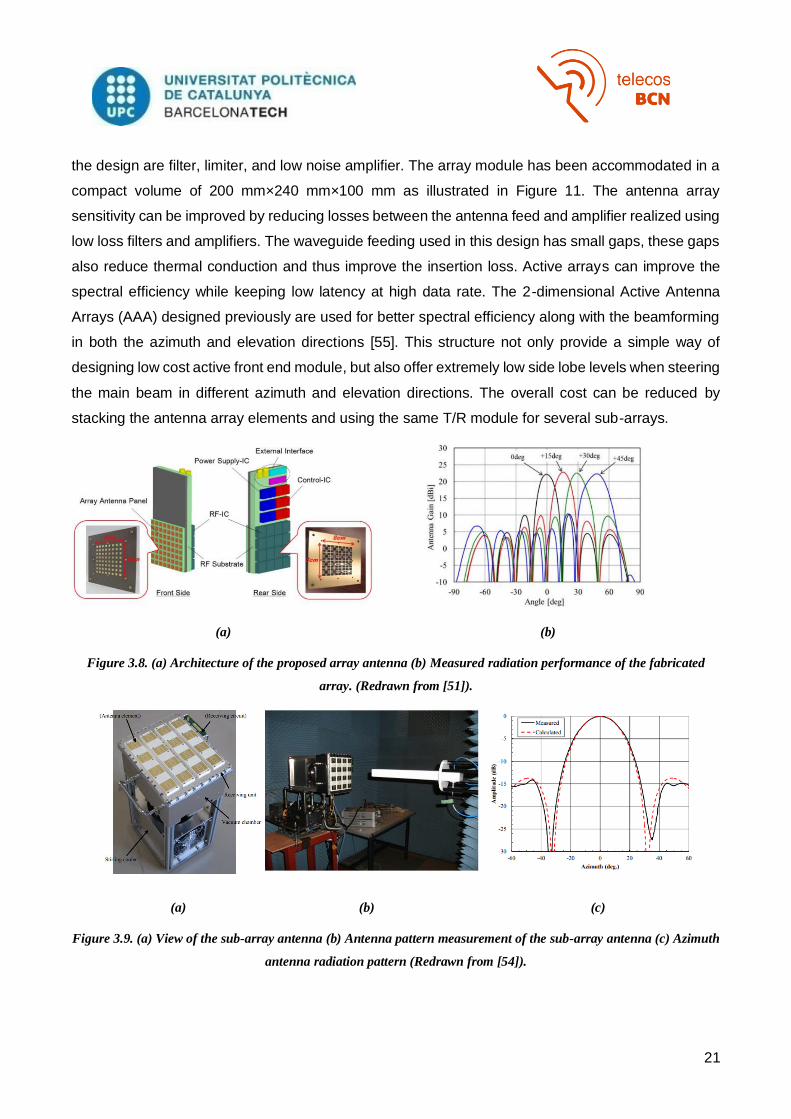
21
the design are filter, limiter, and low noise amplifier. The array module has been accommodated in a
compact volume of 200 mm×240 mm×100 mm as illustrated in Figure 11. The antenna array
sensitivity can be improved by reducing losses between the antenna feed and amplifier realized using
low loss filters and amplifiers. The waveguide feeding used in this design has small gaps, these gaps
also reduce thermal conduction and thus improve the insertion loss. Active arrays can improve the
spectral efficiency while keeping low latency at high data rate. The 2-dimensional Active Antenna
Arrays (AAA) designed previously are used for better spectral efficiency along with the beamforming
in both the azimuth and elevation directions [55]. This structure not only provide a simple way of
designing low cost active front end module, but also offer extremely low side lobe levels when steering
the main beam in different azimuth and elevation directions. The overall cost can be reduced by
stacking the antenna array elements and using the same T/R module for several sub-arrays.
(a) (b)
Figure 3.8. (a) Architecture of the proposed array antenna (b) Measured radiation performance of the fabricated
array. (Redrawn from [51]).
(a) (b) (c)
Figure 3.9. (a) View of the sub-array antenna (b) Antenna pattern measurement of the sub-array antenna (c) Azimuth
antenna radiation pattern (Redrawn from [54]).

22
3.5. High Gain antenna arrays
As discussed previously, high gain and directivity are the key features for designing modern day 5G
antennas working at high data rate and spectral efficiency. Low or moderate gain antennas are not
suitable for mm-wave communication as they dissipate drastically during propagation and can suffer
from interference and distortion. Researchers discovered a variety of techniques such as the use of
dielectric lens antennas [56], fabry-perot antennas [57], metasurface antennas [58], corrugated plate
antennas [59] and other antenna arrays for high gain application. In the literature some very recently
published array antennas fed with SIW networks offers a remarkably high gain of around 25 dBi for
the mm-wave frequency band [60]. The design is made of a multi-layered geometry with 8x8 element
array fed by a modified H-shape network. The H-shape feed along with the T-junction power dividers
are used for equal power transfer in all the four branches with a particularly good isolation of 45 dB
as depicted in Figure 12. With high gain, low mutual coupling and strong interference cancellation
capability, this antenna array is best suitable for the next generation communications.
Some other array antennas offering relatively good gain and a compact, simple structure are
presented below. The design of [61] is a high gain wideband planar array with omnidirectional
radiation pattern. Substrate integrated waveguide (SIC) is used as a power dividing technique to feed
two side by side dipoles radiating in the horizontal plane. The SIC feeding used is very efficient for
splitting the input power into two branches with very low insertion losses. The array is formed by
connecting the output of the transmission line from one element to the input of another element using
meander microstrip line. A dual-fed 1x8 array is formed with in-phase radiation pattern achieved by
controlling the phases of the microstrip line. [62] is a more simple single layer compact 1x16 array
with a gain of 16dB. Along with a good gain a beamforming capability of ±450 can also be achieved.
The proposed design is very compact and can be fit into a cell phone device. Slot arrays also offer a
very promising high gain radiation performance. A long slot high gain antenna array can be designed
on a single layer employing a simple ridge gap waveguide (RGW) feeding [63]. The advantage of this
design is its simple structure, which can be easily fabricated with a lower cost for a mass production.
The radiating slots are fed from both sides in order to produce a single directive beam in the broadside
direction. The proposed antenna has a good realized gain of 23 dB with a side lobe level below -20
dB at the desired frequency, which makes it suitable for the next generation 5G applications. The high
gain is due to the use of two embedded reflectors behaving as a perfect magnetic conductor (PMC)
and perfect electric conductor (PEC), thereby combining the concept of both the leaky wave and slot
antenna.

23
A very well-known method of antenna gain improvement is the use of Partially reflecting surface (PRS)
distant by around half a wavelength from the antenna ground plane. These antennas are usually
referred to as fabry-perot antennas and are based on the principle of multiple interference radiations
emitted by the antenna radiator. A maximum broadside radiation can be obtained when the reflection
waves from both the ground and PRS are in phase according to ray tracing model. An incredibly good
antenna performance can be obtained by optimizing several parameters such as the distance
between the antenna and PRS, thickness of the substrate, and the type of the PRS used. A circularly
polarized fabry-perot high gain MIMO array antenna is designed in [64]. The antenna gain is improved
from 7 dB to almost 14 dB by using PRS spaced by half a wavelength from the antenna ground (Figure
12). The antenna structure is very simple, composed of four truncated patches for circular polarization.
The antenna offers a wideband characteristic and a good port isolation among all the ports. Another
circularly polarized slotted array cavity antenna excited by a simple coaxial probe is designed for high
gain applications [65]. The antenna exhibits a peak gain of 16 dB and radiation efficiency of 96%. SIW
technique is used to build a cavity in one layer of the substrate and the feeding network is avoided to
make the design simpler. The radiating slots are placed half a wavelength apart to introduce the
proper phase change. Resonant cavity antennas on the other hand, are bulky in size and suffers the
challenges of getting wide 3-dB gain bandwidths.
(a) (b) (c)
Figure 3.10. (a) Photograph of 8x8 antenna array (b) Radiation efficiency at 42.5 GHz (c) 3D pattern for various
angles (Redrawn from [60][62]).
(a) (b) (c)
Figure 3.11. (a) View of the proposed cavity antenna (b) Gain comparison of a single element antenna with and
without PRS (c) Radiation pattern of the proposed antenna. (Redrawn from [64]).

24
3.6. Antenna arrays with low Sidelobe Level (SLL)
Similar to gain, reduced sidelobe level is also an important parameter to get improved antenna
performance without signal interference. It is imperative for antenna array to have high gain and low
side lobe levels to work in a high clutter and dense environment (5G). Several tapering pattern
synthesis techniques are used such as Dolph-Chebyshev distribution, Binomial distribution, and
Taylor distribution to reduce side lobe levels. Arrays with uniform weight coefficients have high
sidelobe level, therefore pattern synthesis can be achieved by using a different amplitude coefficient
at each array element. Binomial distribution is usually preferred for small size arrays, but not a good
synthesis technique for large arrays. Taylor distribution can reduce the side lobe level up to a constant
level; however, it is not as effective as the Chebyshev distribution for very large arrays. The
effectiveness of these distributions also depends on the type of application, some are better suited
for some application than the others. The amplitude coefficients can be obtained by designing a feed
network and optimizing its output power to get a particular distribution coefficients.
Several antenna arrays have been designed in the literature employing various distributions for
pattern synthesis. Some authors also compared different feed architectures for optimized results
[66][67]. In [68] microstrip corporate feeds for non-uniform amplitudes linear array is proposed. The
comparison is based on equal and unequal power split junction, both used for a microstrip patch linear
array. The microstrip feed is designed using T junctions, one of the T junctions is designed to allow
unequal splitting of power and another for equal power distribution among the branches. Proper
values of Chebyshev amplitude distribution are obtained from both the designs, which shows that a
feed network with equal split T junction has good side lobe levels while the one with unequal split has
some discrepancies among the measured and the theoretical values for -30 dB SLL (Figure 12).
Another linear microstrip array is designed based on unequal T junction power dividers to achieve a
side lobe level of -25 dB [69]. A simple single layer Chebyshev feed is designed for 1x8 array using
the amplitude weight tapering technique. The feed network must be optimized to get the Chebyshev
polynomials specified for a particular sidelobe level. The proposed design offers a side lobe level of -
22 dB instead of the -25 dB; the difference is due to losses in the transmission line which is not
considered in the theoretical values.
Some series fed planar microstrip patch arrays also promise incredibly good side lobe level reduction.
A compact series fed Dolph-chebyshev array based on periodic stub-loaded slow-wave transmission
line (SW-TL) has been designed [70]. The impedance of any branch can be controlled by modifying
the widths of the loaded stubs which in turn changes the output power amplitude. The slow wave
property of the transmission line reduces the array size and offer very good bandwidth along with a

25
grating-lobes-free broadside radiation pattern. The design exhibits different SLL values for both
simulated (-29.7 dB) and measured (23.7 dB) due to the fabrication and measurement errors. Series
feeding can also be used with simple microstrip line (MTL) for a linear array antenna [71]. Ten-element
array is designed specifically from a double-sided printed dipole as a radiating element for side lobe
level of -30 dB. The design offers a very high gain of 17.5 dB and sidelobe level of -26 dB with good
agreement between the simulated and measured results. Similar to the previous design this array
also uses stubs for controlling the output power, however, it employs MTL feed instead of SW-TL feed.
Microstrip line feeding suffers from a considerable amount of losses and undesirable radiation at
millimeter wave frequencies. Therefore, Substrate integrated waveguide feeding (SIW) is mostly used.
A 28 GHz multi-layer SIW antenna is designed using T-junction power dividers based on a Taylor
beam synthesis [72]. The Taylor polynomials are obtained using four stages of T-junction power
dividers with arbitrary power split ratio. These T-junctions provide unequal power splitting and proper
phases according to the Taylor polynomials without increasing path lengths for phase compensation.
This type of feeding also has a broadband performance as compared to other feeding types. As shown
in Figure 13 the antenna array has13.9 dB gain and a sidelobe level of -20 dB. Despite some
advantages SIW feed networks has the problem of fabrication complexity at mm-wave frequencies.
(a) (b) (c) (d)
Figure 3.12. (a) View of the proposed 12-element array antenna (b) Equal split T-Junction (c) Un-equal split T-
junction (d) Measured and simulated radiation pattern of the array. (Redrawn from [66]).

26
(a) (b) (c)
Figure 3.13. (a) Geometry of the proposed SIW array antenna (b) Prototype of the antenna with coaxial waveguide (c)
Comparison of simulated and measurement radiation patterns at 28 GHz. (Redrawn from [72]).

27
Ref Antenna design Operation
frequency
Peak
Gain
(dB)
Sidelobe
level
(dB)
bandwidth
[11]
35 GHz 17 -19.6 2.6 %
[13]
35 GHz 25.4 -17.6 1.9 %
[28]
28 GHz 15 -15 9 %
[53]
24 GHz 27.2 -12 13 %
[56]
40 GHz 25.8 -25.7 14.6 %
[61]
26 GHz 11 -15 21.1 %
[73]
60 GHz 18 -18.5 7 %
Table 3.1. Comparison of some performance parameters of millimetre wave array antennas

28
4. Array design based on Dolph-Tschebyshev current distribution
Chebyshev synthesis technique reduces the unwanted radiations besides the mainbeam antenna
radiation. Side radiations can be reduced by optimizing the sidelobe level to a specific value. The
Chebyshev current distribution provides an optimum relationship between the beamwidth and
sidelobe level. Chebyshev array was first studied by C.L. Dolph in 1946 [76]. He pointed out that
feeding all the sources with uniform magnitude and phases my result in high gain, but these arrays
suffer from non-optimal beamwidth and high sidelobe levels. Therefore, by feeding the array elements
with different amplitudes and same phases gives optimum sidelobe level and considerably good
beamwidth. Another advantage of Chebyshev array is that the current distributions can be calculated
if the value of sidelobe level or the first null is specified. Dolph Chebyshev proposed the following
formulas for calculating the Tchebyshev polynomials:
𝑇𝑛(𝑧) = 𝐶𝑜𝑠(𝑛 𝑎𝑟𝑐 cos 𝑧) ……………….(1)
Where ‘n’ is polynomials in z, in a set ϕ = arc cos z. Considering polynomial in z, 𝑇𝑛(𝑧) exist for all z,
-∞ ≤ z ≤ ∞.
For an eight element array the current distribution can be calculated as:
𝐹8 (𝑢) = 𝐼1 cos 𝑢 + 𝐼2 cos 3𝑢 + 𝐼3 cos 5𝑢 + 𝐼4 cos 7𝑢 …………………(2)
The polynomials are then derived as:
𝐼4 = 𝑧07 …………(3)
𝐼3 = 7𝐼4 − 7𝑧05 …………(4)
[74]
20 GHz 29.1 -17 15 %
[75]
22 GHz 19 -22 7.8 %

29
𝐼2 =5𝐼3− 14𝐼4 + 14𝑧03 ……...….(5)
𝐼1 =3𝐼2− 5𝐼3+7𝐼4− 7𝑧0 ………..……(6)
Therefore the currents can be easily computed if the value of 𝑧0 is Known.
The Chebyshev distribution is then studied by many researchers, making improvements and
introducing new techniques. In 1994 A.Safaai [77] introduced a new analysis for Chebyshev array
design. The array factor is expressed in terms of cosine or cosine-hyperbolic instead of the Chebyshev
polynomials. Both the broadside and end fire arrays are studied using this technique, providing
simplicity by avoiding the need for trial and error method.
4.1. Single element antenna design
It is imperative to design and analyze the behavior of a single element antenna before designing the
whole array. The single element antenna is designed on a rogers RO5880 substrate with a thickness
of 0.25 mm and relative permittivity of ε𝑟 = 2.2. The substrate is used based on its low losses and
good performance at mm-wave frequency band. This is because the material losses increase with
frequency for substrates with high dielectric constant. Copper is used as a radiating material having
a thickness of 35 µm. Length and width of the patch determine the resonant frequency in terms of the
effective wavelength. In case of the designed antenna, effective resonant lengths have been
determined from the surface current distribution at the resonant frequency band. Length and width of
the effective patch are calculated using 𝐿𝑝 = 0.48𝜆𝑒𝑓𝑓 and 𝑊𝑝 = 0.48𝜆𝑒𝑓𝑓 respectively. These values
are almost half of the effective wavelength (𝜆𝑒𝑓𝑓) at 28 GHz. The effective wavelength is given by the
following well known equation (3).
𝜆𝑒𝑓𝑓 =𝐶
2𝑓𝑟√𝜖𝑒𝑓𝑓 ……………… (7)
Where 𝑓𝑟 is the resonant frequency, C is the speed of light, and 𝜖𝑒𝑓𝑓 is the effective permittivity of the
dielectric given by the equation 8.
∈𝑟𝑒𝑓𝑓=
∈𝑟+1
2+
∈𝑟−1
2√1+ 12ℎ
𝑤
………………….. (8)
The microstrip line impedance and width can also be calculated by the expressions given below. All
these formulas are used in many research articles by multiple authors [78-81]. The antenna feedline

30
is then optimized to get an impedance of 50Ω at the resonant frequency with a slightly different
dimensions than the one calculated using the formulas, to get proper matching.
𝑍0 = 120𝜋
√∈𝑟𝑒𝑓𝑓 (1.393+
𝑤
ℎ+
2
3𝐼𝑛(
𝑤
ℎ+1.4444)
……………………(9)
Also the width of the microstrip line is given by expression 10.
𝑊 = 1
2𝑓𝑟√µ0∈0 √
2
∈𝑟+1 …………………….. (10)
Where W is width of the microstrip line, 𝑓𝑟 is the resonant frequency ∈𝑟 is the relative permitvity, and
µ0 ∈0 are the free space permeability and free space permittivity respectively.
The single element patch antenna is shown in Figure 4.1 with and without the sma connector. All of
the antenna dimensions are summarized in Table 4.1. The antenna has a size of 8 x 7 x 0.28 mm3,
which is decently small. The antenna is fed with a microstrip line with Wf and Lf as the length and
width respectively. Inset feeding is used in order to properly match both the antenna and feed for
efficient power transfer.
(a) (b)
Figure 4.1. (a) Geometry of the propsed single element antenna (b) Antenna with SMA connector.

31
Table 4.1. Overall dimensions of the single element antenna
The return loss of Figure 4.2 shows that the antenna is well matched at 28 GHz with reflection
coefficient value around -25 dB at the centre frequency. The -10 dB bandwidth covers the frequency
band from 27.7 GHz to 28.2 GHz, which is further improved in the final array design. From the surface
current plots of Figure 4.3, it can be seen that the surface currents are in Y-direction, along the length
of the antenna. The surface currents originate from the feed and moves along the patch length and
reverses its direction when the polarity reverses.
Figure 4.2. Return loss of the proposed single element antenna.
Figure 4.3. Surface currents plot of the proposed antenna at 28 GHz.
Lengths Values(mm) Lengths Values(mm) Lengths Values(mm)
Ls 8 Wp 3.5 Lf 2
Ws 7 W1 0.9 Wf 0.3
Lp 3.5 W2 0.85 W3 0.3

32
Figure 4.4. Cartesian Gain radiation pattern of the proposed antenna.
As discussed above; the surface currents are in the direction of Y-axis, therefore the antenna
radiates in perpendicular z-direction with maximum Gain along the boresight. The Polar and
3D plots below illustrate that the antenna is linearly vertical polarized and radiates normal to
the patch surface. The elevation pattern for ϕ = 0 of Figure 4.5 shows that the back radiations
are sufficiently small and is measured to be around -8 dB. The 3D plots of the proposed antenna
illustrate that the antenna has a good gain of 8 dB in the broadside direction. The single element
antenna is also very efficient in terms of radiation, having radiation efficiency of 95% at the centre
frequency.
Figure 4.5. Polar radiation (Gain) pattern of the proposed antenna at 28 Ghz.

33
Figure 4.6. 3-dimensional Gain radiation plots of the proposed antenna from two different views.
4.2. Chebyshev feed network design
The desired sidelobe level and beamwidth can be obtained by array synthesis using the Chebyshev
polynomials. The required number of radiating elements must be determined for the specified value
of gain and sidelobe level. Chebyshev polynomials can be derived from the above-mentioned
expressions, before designing the array feed network. Two main types of the feed network used are
the series feed [82] and incorporate feed [83] structure. Although, the series feeding has a very short
overall transmission length with lower transmission losses, the incorporate feeding is more efficient
for very dissimilar power distribution. Therefore, incorporate feeding techniques are preferred for
Chebyshev feed network design. The unequal power distribution is realized by the use of T-junctions
each having a different impedance. The output power from the junction can be controlled by changing
the width of the line which in turn affects the line impedance.
Feed network for 8x1 array is designed on a RO5880 substrate with permittivity of ∈𝑟= 2.2 and
thickness of 0.25 mm. The primary objective of the feed design was to achieve the calculated
Chebyshev polynomials at the output of each branch of the feed network. The calculated theoretical
power amplitudes for eight element array with sidelobe level of -25 dB is summarized in Table 4.2.
As for even number of elements the amplitudes on both the sides of the array is the same. Therefore,
the first four branches is designed and mirrored on the other side to ensure both the sides have the
same amplitudes and phases as illustrated in Figure 4.7. The simulated s-parameter values of the
proposed feed network is shown in Figure 4.8, and the obtained amplitude values are also listed in
Table 4.2. It can be seen that the simulated values are quite uniform. Although by comparing the
simulated amplitude values to the one calculated in the theory; shows that there is a difference of

34
around 1.2 dB in each value for all the eight ports. The difference is due to the losses of the
transmission line, which are not considered while calculating the theoretical values.
Table 4.2. Theoretical and proposed current amplitudes for SLL = -25 db
The phases, however, must be all the same for each output port of the feed network. The Chebyshev
distribution only effects the amplitudes, but the phases remains the same. Therefore, for better results
it is necessary to have all the output signals in phase. The values of the simulated phases are
illustrated in Figure 4.9, which shows that all the signals are almost in phase. There is a very small
difference in phases which is almost negligible for this particular array type. The very small difference
in phases is due to the different size width and length of each line. The input of the feed network is
fed by 50Ω line, and the output of each port is controlled by impedance matching to get the appropriate
amplitude excitation at each of the eight output ports [84]. In order to reduce the line losses in the
feed network the edges of each branch are trimmed as shown in the zoomed view of Figure 4.7, so
that the power flows smoothly within the feedline.
Figure 4.7. Proposed chebyshev feed network.
Elements N0. 1 2 3 4 5 6 7 8
Theoretical amplitude
distribution (dB)
-14.8 -11.0 -7.9 -6.4 -6.4 -7.9 -11.0 -14.8
Simulated amplitude
distribution (dB)
-16.0 -12.1 -9.3 -7.6 -7.6 -9.3 -12.1 -16.0

35
Figure 4.8. Simulated amplitudes of all the eight ports.
Figure 4.9. Simulated phases for all the output ports.
4.3. Array antenna design
The chebyshev array antenna is designed by combining both the optimized feed network and the
patch radiating elements to form 8x1 array. Two types of array designs have been proposed based
on the performance parameters. The designs are analyzed in both Computer Simulation Technology
(CST) and High frequency Structure Simulation (HFSS). The results are then compared from both the
simulation software’s showing good performance agreement. The antenna centre frequency is 28
GHz, with the design specifications of broadside radiation at θ = 00, above 12 dB Gain and sidelobe
level of at least below -15 dB. In order to achieve the desired sidelobe level and radiation pattern for
a given number of elements the array factor can be designed using the given chebyshev amplitude
coefficients [85]. Dolph chebyshev proposed two different expressions for linear broadside array
synthesis based on the number of radiating elements. For an even number of elements (2N) there is
no radiating element at the centre of the array while in case of an odd number of elements (2N+1)

36
there is a centre radiating element also. By feeding these arrays with unequal power distribution the
current the field patterns can be expressed by the given expressions.
𝐸2𝑁(𝜃) = ∑ 𝐼𝑘𝐶𝑜𝑠 2𝑘+1
2(
2𝜋𝑑
𝜆𝑁−1𝐾=0 ) 𝑆𝑖𝑛𝜃 …………………. (11)
𝐸2𝑁+1(𝜃) = ∑ 𝐼𝑘𝐶𝑜𝑠 𝑘(2𝜋𝑑
𝜆𝑁𝐾=0 ) 𝑆𝑖𝑛𝜃 ………..……………(12)
The above expressions are true only if all the signals are in phase along the array. Also, the elements
of the array must be equidistant.
4.3.1. First array design configuration
A single layer eight element array antenna is designed with a compact size of 45 mm x 15 mm. The
array is realized by designing unequal power distribution feed network, an optimized single element
patch antenna and integrating them to form chebyshev array as illustrated in Figure 4.10. This design
offers a realized Gain of 12.1 dB and sidelobe level of around -16 dB with a broadside radiation pattern.
A single layer of Rogers 5880 substrate is used with permittivity of ∈𝑟= 2.2 and thickness of 0.25 mm.
Inset feeding is used for better matching and wide bandwidth operation. The inset dimensions have
been modified to obtain a good antenna performance. The inter-element distance is 0.7 times the
guided wavelength at 28 GHz as a centre frequency. The input of the array is fed with a 50Ω power
source and the power is then distributed according to the unequal current distribution presented above.
The proposed design has a simple feed network, single layer configuration and is very easy to
fabricate.
Figure 4.10. Geometry of the first array design configuration.

37
4.3.2. Second array design configuration
The first design is modified to form a second antenna configuration to further improve the antenna
performance parameters. Two Rogers 5880 substrates with the same relative permittivity (∈𝑟= 2.2)
and 0.25 mm thickness is used having the feed network sandwiched between them. The radiating
patches are placed on top of the second substrate fed by vias connecting the radiating elements to
the feed network. Unlike the first design no inset feeding is used in this configuration as shown in
Figure 4.11. This design improves the antenna gain from 12 dB to 14 dB and the sidelobe level of -
19 dB. The design also has the advantage of having the same dimensions as the previous one except
the use of one more substrate that increases the array thickness by 0.25 mm. The inter-element
distance and the radiating element size is also kept the same.
Figure 4.11. Geometry of the second array design configuration.
5. Results
Each of the design is simulated and analyzed both in Computer Simulation Technology (CST) and
High Frequency Structure Simulation (HFSS). Results from both the software’s are also compared
with each other showing good performance agreement. In CST, the frequency domain solver is used
for all simulations. The simulation results of some important antenna parameters are listed below.

38
5.1. Simulation results of the fist antenna configuration
5.1.1.1 Return loss
From the return loss diagram of Figure 5.1 it can be seen that the antenna is perfectly matched at 28
GHz. The array antenna offers below -10 dB impedance bandwidth between 27.4 GHz and 28.8 GHz
with an overall bandwidth of 1.4 GHz and return loss value of -44 dB at around 28.1 GHz. The
matching of the antenna can also be verified from the smith chart impedance plot of Figure 5.2. The
impedance at 28 GHz is 49.5 Ω which is very close to 50 Ω, also the impedance at 27.4 GHz and
28.8 GHz is 45.9 Ω and 36.2 Ω respectively. These values are close to the decimal point 1 on the
smith chart which represent matching at 50 Ω impedance.
Figure 5.1. Reflection coefficient of the proposed first array design.
Figure 5.2. Smith chart representation of the proposed antenna impedance.

39
5.1.1.2 Radiation pattern
The proposed antenna radiates linearly in the broadside direction with a gain of 12.2 dB and sidelobe
level of almost -16 dB. 3D plots of Figure 5.3. Shows that the array radiates in the theta (z-axis)
direction with suppressed side lobes in the direction other than theta. It is also worth mentioning that
the back lobe radiation is relatively small upto an acceptable value.
Figure 5.3. Different views of 3D radiation plots at 28 GHz.
The far field gain radiation pattern for both 𝜙 = 00 (xz plane) and ϕ = 900 (yz plane) are shown in
Figure 5.4, highlighting that the antenna has a maximum radiation in the broadside direction of θ =
00. It can also be noticed that the sidelobe level value is -16 dB. The proposed antenna has a stable

40
radiation pattern in the z-plane. From the radiation pattern plots, it is clear that the chebyshev
synthesis helps in suppressing the sidelobe level of the proposed array antenna.
(a)
(b)
Figure 5.4. Cartesian plots for far-field Gain radiation pattern (a) xz-plane (b) yz-plane
For further clarification, the polar radiation plots are also included (Figure 5.5), showing that the
antenna radiates at θ = 00 as a reference plane. The radiation gain of the antenna is maximum in the
boresight direction. The main lobe magnitude is slightly different than that of the cartesian and 3D
radiation plots, but the magnitude of the SLL is the same.

41
Figure 5.5. Polar radiation plot at 𝝓 = 𝟎𝟎 and resonance frequency of 28 GHz.
5.1.1.3 Surface current plots
The 2D surface current plots of Figure 5.6 highlights the effective resonant lengths. It can be seen
that the surface currents are along the Y-direction similar to the single element antenna discussed
earlier, with a maximum density along the length of the patch. It is evident from the plots that the
antenna is linearly polarized radiating normal to the z-plane. Also, the magnitude of the cross-
polarization is less than that of the co-polarization for the desired polarization direction. The 2D
radiation plot for the far-field gain is also represented in Figure 5.7, The radiation intensity is only high
in the middle between θ = −300 and θ = +300 at 28 GHz.
Figure 5.6. Surface currents distribution plot of the proposed single layer antenna.

42
Figure 5.7. 2D Gain radiation pattern of the proposed single layer antenna array.
5.1.2 HFSS results of the first array design
The proposed array antenna is also simulated and analyzed in HFSS and the results were compared
with that obtained from CST. The return loss of Figure 5.9 shows that the antenna offers an impedance
bandwidth of 2.3 GHz covering from 26.8 GHz to 29.1 GHz. Which is increased by almost 3% (In
terms of fractional bandwidth) in comparison to the one simulated using CST.
Figure 5.8. HFSS design of the first configuration array antenna.

43
Figure 5.9. Return loss of the proposed array antenna.
Comparison of the radiation pattern shows that the gain of the proposed array is increased from 12.2
dB to 12.8 dB, while keeping the sidelobe level almost similar to the simulation results obtained from
CST. All the radiation plots illustrated below shows that the sidelobe level is around -16 dB. However,
both the main lobe and the sidelobe magnitudes have been increased by around 0.6 dB, while keeping
the SLL ratio the same.
Figure 5.10. Far-field Cartesian gain radiation plot at 𝝓 = 𝟎𝟎.

44
Figure 5.11. Far-field Cartesian gain radiation plot at 𝝓 = 𝟗𝟎𝟎.
The polar plots of Figure 5.12 show that the array antenna has a main lobe radiation exactly in the
θ = 00 direction. The sidelobes and backlobe radiation is also clearly visible in the diagram. It is clear
that the radiation pattern is the same as described above for the first array design configuration with
the main lobe radiation in the z-direction and the current flow in the positive y-direction.
Figure 5.12. 2D polar gain radiation plot at 28 GHz.

45
Figure 5.13. 3D radiation plots of the proposed array at 28 GHz simulated in HFSS.
5.2 Simulation results of the second design configuration
The array antenna performance is further improved by modifying the first antenna array design. The
modification includes the addition of one extra substrate with the same specifications as the one used
in the previous design, and the addition of Vias at each output port to feed the radiating elements.
Some of the noticeable improvements in the results are discussed below.
5.2.1.1 Return Loss
A good performance improvement in the impedance bandwidth is observed. Figure 5.8 shows that
the impedance bandwidth is enhanced from 5.0% to 12.3%. This new design covers a -10 dB
bandwidth of almost 3.5 GHz from 25.1 GHz to 28.6 GHz covering most of the millimetre wave
frequency band.
Figure 5.14. Reflection coefficient of the second antenna array design.

46
5.2.1.2 Radiation pattern
The antenna gain is improved from 12.2 dB to 14 dB as illustrated in the 3D radiation plots of Figure
5.9. The sidelobe level is also improved from -16 dB to -19.2 dB (Figure 5.10), which is a considerable
amount of improvement. Similar to the first design the second design configuration also has a main
lobe radiation in the direction of θ = 00 as a reference plane. Although the main lobe magnitude is not
maximum exactly at θ = 00 unlike the previous design. The direction of main lobe is shifted by a few
degrees to the left side (-y-axis), however there is a very small difference in the main lobe radiation
magnitude of both the shifted angel and θ = 00.
Figure 5.15. Different views of 3D radiation plots at 28 GHz for the second design
configuration.

47
Figure 5.16. Far-field cartesian Gain radiation plot second antenna array at 28 GHz.
5.2.1.3 Surface current plots
The 2D surface current plots indicate that the current direction is along y-axis, similar to the previous
design. Although the inset feeding is not used, the radiating elements are fed by vias, connecting the
feedline with the patches. The maximum amount of current density can be seen around the vias as
depicted in Figure 5.11. Due to the same current’s direction the polarization of both the designs is
also the same.
Figure 5.17. Surface currents distribution plot of the second design array antenna.
5.2.2 HFSS results of the second array design
The second array antenna design is also simulated in HFSS, in order to compare with the results
obtained from CST. The return loss obtained is almost the same with -10 dB impedance bandwidth
covering from 25.3 GHz to 28.6 GHz. Although the minimum value of the reflection coefficient in the

48
resonance bandwidth is -25 dB around 28.1 GHz while in the case of CST the minimum value obtained
is -42 dB at 26.7 GHz, which is considered almost similar, as it does not change the antenna
performance as long as the reflection coefficient magnitude is less than -10 dB.
Figure 5.18. Geometry of the second array antenna configuration in HFSS.
Figure 5.19. Return loss of the antenna simulated in HFSS.
These has no considerable change noticed in terms of radiation pattern from both the simulation
software’s. The antenna gain as depicted below is 14.2 dB which is similar to the design simulated
with CST (14 dB), Also the sidelobe level in both the cases is -19 dB. As illustrated in Figure 5.20, the
main lobe magnitude is around 14 dB and the sidelobe magnitude is almost -5 dB.

49
Figure 5.20. Far-field Cartesian gain radiation plot at 𝝓 = 𝟗𝟎𝟎.
Figure 5.21. 3D Gain radiation plots of the proposed array antenna at 28 GHz.
It is clear from all the simulation results listed above that most of the performance parameters are
very similar for both the designs by comparing results from the different simulation software’s.
However, there has been some small discrepancies observed in the simulation results. This is
because these simulation software’s are based on different computational techniques. CST is based
on Finite Integration Technique (FIT), while HFSS is based on Finite Element Method (FEM), which
is the reason for small differences in the results for the same antenna model. Some other important
reasons for achieving slightly different results are the use of the different geometry mesh algorithm,
different material properties, and using different boundary conditions.

50
6 Fabrication and Testing
The proposed array antenna is fabricated to characterize and validate the simulation results. Antenna
PCB can be manufactured using several fabrication techniques [86]. PCB etching is one of the most
widely used antenna fabrication techniques for antenna manufacturing [87, 88]. The etching process
can be performed in a number of ways, including the use of acid which is more economical. The PCB
manufacturing using an acid etching bath technique includes several steps. The proposed array
antenna is fabricated by first exporting the simulation design as .dxf file. The exported file is then
imported to a CAD software for printing it on a paper using a laser printer. The printed design is then
placed on the copper PCB by aligning it properly on the surface and passing through laminator such
that the antenna structure is properly printed on the copper plate. The paper is removed by putting
the PCB board in water for a few minutes. Finally, the copper plate is dipped in the etching solution
for around 40 minutes until all the copper around the circuit is completely dissolved. The final design
is then dried after washing with water and the transferred ink on the antenna surface is removed by
rubbing, using alcohol solution. The fabricated prototype is shown in Figure 6.1 below.
Figure 6.1. Prototype of the proposed first configuration array antenna.
6.1 Measured reflection coefficient results
The return loss of the proposed antenna is measured using a ROHDE&SCHWARZ vector network
analyzer, as shown in Figure 6.2. The impedance bandwidth of the antenna, considering the main
resonance band ranges from 27.5 GHz to 30.5 GHz. Which is almost similar to the one obtained from

51
the simulation results. However, other resonances besides the main resonance band, have been
shifted below -10 dB, making the resonance bandwidth more wider. There are several reasons for
this change, the SMA connector, introduces some losses, which is usually not considered during
simulations. Fabrication tolerance and material losses also produce a considerable amount of change
in the results. The calibration of the network analyzer is also one of the main reasons for getting
different simulation and measured results. The contribution of these losses improves the measured
return loss of the antenna and leads to the different measured and simulated results. It is also worth
noticing that the s-parameter results calculated using HFSS are more similar to the measured results
than the one simulated using CST.
Figure 6.2. Measurement system for the return loss of the proposed antenna.

52
Figure 6.3. Comparison graph of the simulated and measured return loss.
7 Budget
This project is carried out at the Intelligent Wireless Technology (IWT) lab of the university of Alberta
Canada. The lab facility was used for simulation, fabrication, and measurements, therefore there has
no major cost associated with the project. Although, the substrate materials were purchased for the
antenna fabrication, that costs around $120.
8 Conclusions and future development
Recent progress on high gain array antennas are setting the stage for the next generation of cellular
evolution. High gain, low sidelobe level array antennas are the most promising class of antennas to
better perform in the future dense and high data rate communication environment. Array antennas
received a great boost since the development of phased array antennas that continuously increased
while addressing to the high propagation losses of mm-waves for the fifth generation (5G) wireless
links. This dissertation aims to design a high gain, low sidelobe level (SLL) array antenna and to
provide a summary and classification of the recent advancement on the design, architecture, and
working principles of the antenna arrays. Two different designs of a linear array antenna based on
Chebyshev distribution have been proposed and analyzed at 28 GHz. The array is based on unequal
power distribution among the antenna elements. The non-uniform amplitude excitation needs unequal
power split junction power dividers for the realization of the Chebyshev feed network. The first array
design is then modified, and the performance parameters have been improved. A Gain of 12.2 dB
and SLL of -16 dB is obtained from the first Chebyshev array design configuration, which is then
-50
-40
-30
-20
-10
0
22 24 26 28 30 32
Ret
urn
Lo
ss (
dB
)
Frequency (GHz)
Comparison of simulated and measured S11
Simulated S11
Measured S11

53
improved to a maximum gain of 14 dB and SLL of -19 dB. Also, the impedance bandwidth is enhanced
from 5% to 13%. The behavior of the designed array antennas is studied in both the CST and HFSS.
Results from both the EM software’s have been compared, showing good performance agreement.
Although there is a small discrepancy in the results, due to the different computational techniques
used by both the simulation software’s. The first array antenna design is fabricated and tested to
validate the simulation results. The modified design, however, is not fabricated due to the time
constraints. The proposed array antenna possesses several advantages such as high gain, low
sidelobe level, wide bandwidth, compact structure, low cost and is easy to fabricate.
Array antennas are considered to be a core technology for the next generation networks due to its
characteristics such as high efficiency, better signal quality, wide area coverage and beamforming
capability. The antenna requirements increase with the increase in data rate and interference-less
communication requirements, which requires more sophisticated array antennas. The proposed work
can be extended to a subarray MIMO design to further improve the gain and SLL performance, to fulfil
the stringent demands of the next generation networks. Moreover, the beamforming capability will be
investigated to have a better control of the antenna radiation performance.
Another possible extension is the integration of the proposed Chebyshev array antenna with Fabry-
Perot cavity (FPC) antenna. FPC antennas posses high gain with relatively high sidelobe level, while
on the other hand Chebyshev array antennas have low sidelobe level and a reasonable gain.
Therefore, a very high gain and suppressed sidelobe level performance can be achieved by
combining both the antennas into a single design architecture. In addition, some other techniques will
be investigated for improving the impedance bandwidth and polarization of the proposed antenna.

54
Bibliography
[1]. T. S. Rappaport et al., ‘‘Millimeter wave mobile communications for 5G cellular: It will work!’’ IEEE
Access, vol. 1, pp. 335–349, May 2013.
[2]. Final Acts WRC-15 in World Radiocommunication Conference, document 190-15, Geneva,
Switzerland, Apr. 2016.
[3]. M. M. Honari, R. Mirzavand, J. Melzer and P. Mousavi, "A New Aperture Antenna Using Substrate
Integrated Waveguide Corrugated Structures for 5G Applications," in IEEE Antennas and
Wireless Propagation Letters, vol. 16, pp. 254-257, 2017.
[4]. Peize, Zhang. (2019). Radio propagation and wireless coverage of LSAA-based 5G millimeter-
wave mobile communication systems, 2019.
[5]. F. Sohrabi, W. Yu, “Hybrid digital and analog beamforming design for large-scale antenna arrays,”
IEEE Journal of Selected Topics in Signal Processing, vol. 10, no. 3, 2016.
[6]. S. P. Skobelev, "Some Features of the Overlapped Subarrays Built Up of Beam-Forming Matrices
for Shaping Flat-Topped Radiation Patterns," in IEEE Transactions on Antennas and Propagation,
vol. 63, no. 12, pp. 5529-5535, Dec. 2015.
[7]. S. Bildik, S. Dieter, C. Fritzsch, W. Menzel and R. Jakoby, "Reconfigurable Folded Reflectarray
Antenna Based Upon Liquid Crystal Technology," in IEEE Transactions on Antennas and
Propagation, vol. 63, no. 1, pp. 122-132, Jan. 2015.
[8]. S. E. Hosseininejad, N. Komjani,H.Oraizi,and M. T. Noghani, “Optimum design of SIW longitudinal
slot array antennas with specified radiationpatterns,”ACESJ.,vol.27,no.4,pp.320–325,Apr.2012.
[9]. Y. Li, Z. Zhang, C. Deng, Z. Feng and M. F. Iskander, "2-D Planar Scalable Dual-Polarized Series-
Fed Slot Antenna Array Using Single Substrate," in IEEE Transactions on Antennas and
Propagation, vol. 62, no. 4, pp. 2280-2283, April 2014.
[10]. M. Ikram, N. Nguyen-Trong and A. M. Abbosh, "Realization of a Tapered Slot Array as Both
Decoupling and Radiating Structure for 4G/5G Wireless Devices," in IEEE Access, vol. 7, pp.
159112-159118, 2019.
[11]. B. Liu et al., "A 45$^\circ$ Linearly Polarized Slot Array Antenna With Substrate Integrated
Coaxial Line Technique," in IEEE Antennas and Wireless Propagation Letters, vol. 17, no. 2, pp.
339-342, Feb. 2018.
[12]. R. Lian, Z. Wang, Y. Yin, J. Wu and X. Song, "Design of a Low-Profile Dual-Polarized Stepped
Slot Antenna Array for Base Station," in IEEE Antennas and Wireless Propagation Letters, vol.
15, pp. 362-365, 2016.

55
[13]. X. Jiang, Z. Zhang, Z. Tian, Y. Li and Z. Feng, "A Low-Cost Dual-Polarized Array Antenna Etched
on a Single Substrate," in IEEE Antennas and Wireless Propagation Letters, vol. 12, pp. 265-268,
2013.vbc
[14]. F. Boccardi, R. W. Heath, A. Lozano, T. L. Marzetta and P. Popovski, "Five disruptive technology
directions for 5G," in IEEE Communications Magazine, vol. 52, no. 2, pp. 74-80, February 2014.
[15]. G. Yang, J. Li, D. Wei and R. Xu, "Study on Wide-Angle Scanning Linear Phased Array Antenna,"
in IEEE Transactions on Antennas and Propagation, vol. 66, no. 1, pp. 450-455, Jan. 2018.
[16]. R. W. Kindt and W. R. Pickles, “All-metal flared-notch array radiator for ultrawideband
applications,” Naval Res. Lab., Washington, DC, USA, Tech. Rep. NRL/MR/5310–10-9279, Sep.
2010.
[17]. J. J. Lee, S. Livingston, and R. Koenig, “Performance of a wideband (3–14 GHz) dual-pol array,”
in Proc. IEEE Antennas Propag. Soc. Symp., vol. 1. Jun. 2004.
[18]. W. F. Moulder, K. Sertel, and J. L. Volakis, “Superstrate-enhanced ultrawideband tightly coupled
array with resistive FSS,” IEEE Trans. Antennas Propag., vol. 60, no. 9, pp. 4166–4172, Sep.
2012.
[19]. J. Bai et al., “Optically driven ultrawideband phased array with an optical interleaving feed
network,” IEEE Antennas Wireless Propag. Lett., vol. 13, pp. 47–50, 2014.
[20]. D. D. Ross et al., "Low-Profile High-Power Optically Addressed Phased Array Antenna," in
Journal of Lightwave Technology, vol. 35, no. 18, pp. 3894-3900, 15 Sept.15, 2017.
[21]. F. Demmerle and W. Wiesbeck, "A biconical multibeam antenna for space-division multiple
access," in IEEE Transactions on Antennas and Propagation, vol. 46, no. 6, pp. 782-787, June
1998.
[22]. J. Brady, N. Behdad, and A. M. Sayeed, “Beamspace MIMO for millimeter-wave communications:
System architecture, modeling, analysis, and measurements,” IEEE Trans. Antennas Propag.,
vol. 61, no. 7, pp. 3814–3827, Jul. 2013.
[23]. H. Yagi, S. Uda, “Projector of the Sharpest Beam of Electric Waves,” Proc. Imp. Acad. (Tokyo)
Vol 2, p 49 (1926).
[24]. M. 1. Skolnik, “Survey of Phased Array Accomplishments and Requirements for Navy Ships,” in
Phased Array Antennas. Edited by A. A. Oliner and G. H. Knittel, Artech House, Inc., pp. 15-20.
[25]. C. Balanis, Antenna Theory and Design, Third Edition, New York, Wiley, 2005.
[26]. T. Friis and W.D. Lewis, “Radar Antennas,” Bell System Technical Journal, Vol XXVI, April 1947,
No. 2, pp. 219 – 317.
[27]. A.G. Fox, “An adjustable wave-guide phase changer,” Proc IRE., Vol 35, pp. 1489-1498, Dec
1947.

56
[28]. B. Yu, K. Yang, C. Sim and G. Yang, "A Novel 28 GHz Beam Steering Array for 5G Mobile Device
With Metallic Casing Application," in IEEE Transactions on Antennas and Propagation, vol. 66,
no. 1, pp. 462-466, Jan. 2018.
[29]. N. Ojaroudiparchin, M. Shen, S. Zhang and G. F. Pedersen, "A Switchable 3-D-Coverage-Phased
Array Antenna Package for 5G Mobile Terminals," in IEEE Antennas and Wireless Propagation
Letters, vol. 15, pp. 1747-1750, 2016.
[30]. D. W. Prather et al., "Optically Upconverted, Spatially Coherent Phased-Array-Antenna Feed
Networks for Beam-Space MIMO in 5G Cellular Communications," in IEEE Transactions on
Antennas and Propagation, vol. 65, no. 12, pp. 6432-6443, Dec. 2017.
[31]. S. Shi et al., “Conformal wideband optically addressed transmitting phased array with photonic
receiver,” J. Lightw. Technol., vol. 32, no. 20, pp. 3468–3477, Oct. 15, 2014.
[32]. M. R. Konkol et al., “High-power photodiode-integrated-connected array antenna,” J. Lightw.
Technol., vol. 35, no. 10, pp. 2010–2016, May 15, 2017.
[33]. S. Zhang, I. Syrytsin and G. F. Pedersen, "Compact Beam-Steerable Antenna Array With Two
Passive Parasitic Elements for 5G Mobile Terminals at 28 GHz," in IEEE Transactions on
Antennas and Propagation, vol. 66, no. 10, pp. 5193-5203, Oct. 2018, doi:
10.1109/TAP.2018.2854167.
[34]. R. Vaughan, “Switched parasitic elements for antenna diversity,” IEEE Trans. Antennas Propag.,
vol. 47, no. 2, pp. 399–405, Feb. 1999.
[35]. M. Imbert, J. Romeu, M. Baquero-Escudero, M. Martinez-Ingles, J. Molina-Garcia-Pardo and L.
Jofre, "Assessment of LTCC-Based Dielectric Flat Lens Antennas and Switched-Beam Arrays for
Future 5G Millimeter-Wave Communication Systems," in IEEE Transactions on Antennas and
Propagation, vol. 65, no. 12, pp. 6453-6473, Dec. 2017.
[36]. M. Imbert, A. Papió, F. D. Flaviis, L. Jofre, and J. Romeu, “Design and performance evaluation of
a dielectric flat lens antenna for millimeterwave applications,” IEEE Antennas Wireless Propag.
Lett., vol. 14, pp. 342–345, 2015.
[37]. G. F. Hamberger, A. Drexler, S. Trummer, U. Siart and T. F. Eibert, "A planar dual-polarized
microstrip 1D-beamforming antenna array for the 24GHz ISM-band," 2016 10th European
Conference on Antennas and Propagation (EuCAP), Davos, 2016.
[38]. P. Afanasyev, S. Matitsine, V. Sledkov, P. Lagoiski, L. Matytsine, T. DeMarco, and T.-T. Chia,
‘‘Multi-beam Luneburg lens antenna for cellular communications,’’ in Proc. 9th Eur. Conf.
Antennas Propag. (EuCAP), Apr. 2015.

57
[39]. H. Chou and Z. Tsai, "Near-Field Focus Radiation of Multibeam Phased Array of Antennas
Realized by Using Modified Rotman Lens Beamformer," in IEEE Transactions on Antennas and
Propagation, vol. 66, no. 12, pp. 6618-6628, Dec. 2018.
[40]. H. Chou, Z. Tsai and S. Panigrahi, "Tri-Focal Configuration of Three-Dimensional Metallic
Waveguide-Array Lens Antennas of Rotman Lens Concept for Multi-Beam Applications," in IEEE
Access, vol. 7, pp. 144524-144535, 2019.
[41]. G. W. Kant, P. D. Patel, S. J. Wijnholds, M. Ruiter and E. van der Wal, "EMBRACE: A Multi-Beam
20,000-Element Radio Astronomical Phased Array Antenna Demonstrator," in IEEE Transactions
on Antennas and Propagation, vol. 59, no. 6, pp. 1990-2003, June 2011.
[42]. L. Kuai et al., "A N260 Band 64 Channel Millimeter Wave Full-Digital Multi-Beam Array for 5G
Massive MIMO Applications," in IEEE Access, vol. 8, pp. 47640-47653, 2020.
[43]. M. Karimipour, N. Komjani and I. Aryanian, "Broadband, dual-band reflectarray with dual
orthogonal polarisation for single and multi-beam patterns," in IET Microwaves, Antennas &
Propagation, vol. 13, no. 12, pp. 2037-2045, 2 10 2019.
[44]. W. Hong et al., "Multibeam Antenna Technologies for 5G Wireless Communications," in IEEE
Transactions on Antennas and Propagation, vol. 65, no. 12, pp. 6231-6249, Dec. 2017.
[45]. Shih-Chieh Yen and Tah-Hsiung Chu, "A retro-directive antenna array with phase conjugation
circuit using subharmonically injection-locked self-oscillating mixers," in IEEE Transactions on
Antennas and Propagation, vol. 52, no. 1, pp. 154-164, Jan. 2004.
[46]. L. Chen, T. Zhang, S. Liu and X. Shi, "A Bidirectional Dual-Frequency Retrodirective Array for
Full-Duplex Communication Applications," in IEEE Antennas and Wireless Propagation Letters,
vol. 11, pp. 771-774, 2012.
[47]. A. Yao, W. Wu and D. Fang, "Study on Reconfigurable Coaperture Antenna Arrays Based on
Time-Modulation and Retrodirective Techniques," in IEEE Transactions on Antennas and
Propagation, vol. 64, no. 5, pp. 1713-1724, May 2016.
[48]. J. A. Vitaz, A. M. Buerkle and K. Sarabandi, "Tracking of Metallic Objects Using a Retro-Reflective
Array at 26 GHz," in IEEE Transactions on Antennas and Propagation, vol. 58, no. 11, pp. 3539-
3544, Nov. 2010.
[49]. A. Chepala, V. Fusco and N. Buchanan, "Active Circular Retro-Directive Array," in IEEE
Transactions on Antennas and Propagation, vol. 67, no. 10, pp. 6677-6679, Oct. 2019.
[50]. V. F. Fusco and N. Buchanan, "Retrodirective Array Performance in the Presence of Near Field
Obstructions," in IEEE Transactions on Antennas and Propagation, vol. 58, no. 3, pp. 982-986,
March 2010.

58
[51]. S. Yamaguchi, H. Nakamizo, S. Shinjo, K. Tsutsumi, T. Fukasawa and H. Miyashita,
"Development of active phased array antenna for high SHF wideband massive MIMO in 5G,"
2017 IEEE International Symposium on Antennas and Propagation & USNC/URSI National Radio
Science Meeting, San Diego, CA, 2017.
[52]. P. Xingdong, H. Wei, Y. Tianyang and L. Linsheng, "Design and implementation of an active
multibeam antenna system with 64 RF channels and 256 antenna elements for massive MIMO
application in 5G wireless communications," in China Communications, vol. 11, no. 11, pp. 16-23,
Nov. 2014.
[53]. Q. Wang, W. M. Zou, M. P. Jin, X. L. Zhang and L. Chen, "A Low-Cost Thin Active Phased Array
for 5G Applications," 2019 12th UK-Europe-China Workshop on Millimeter Waves and Terahertz
Technologies (UCMMT), London, United Kingdom, 2019.
[54]. T. Kumamoto, H. Kayano, N. Shiokawa, K. Nakayama, T. Kawaguchi and M. Shinonaga, "High-
sensitivity receiving sub-array module with HTS filters for an active phased array antenna," 2013
IEEE International Symposium on Phased Array Systems and Technology, Waltham, MA, 2013.
[55]. Kumar, Atul & Bartelt, Jens & Barreto, Andre Noll & Fettweis, Gerhard. (2019). 2D Active Antenna
Array Design for mMIMO to Improve Spectral and Energy Efficiency. 10.1109/5GWF.2019.
[56]. Saghlatoon, Hossein & Honari, Mohammad Mahdi & Aslanzadeh, Samira & Mirzavand, Rashid.
“Electrically-Small Luneburg Lens for Antenna Gain Enhancement Using New 3D Printing Filling
Technique”. AEU - International Journal of Electronics and Communications, 2020.
[57]. A. Goudarzi, M. Movahhedi, M. M. Honari, H. Saghlatoon, R. Mirzavand and P. Mousavi,
"Communication Wideband High-Gain Circularly-Polarized Resonant Cavity Antenna with a Thin
Complementary Partially Reflective Surface," in IEEE Transactions on Antennas and Propagation,
2020.
[58]. S. S. Bahramipour, K. Afrooz, M. M. Honari, R. Mirzavand and P. Mousavi, "Gradient and
Huygens’ Metasurface Design and Analysis Based on Transmission Line Theory," in IEEE
Transactions on Antennas and Propagation, 2020.
[59]. M. M. Honari, R. Mirzavand and P. Mousavi, "A High-Gain Planar Surface Plasmon Wave
Antenna Based on Substrate Integrated Waveguide Technology With Size Reduction," in IEEE
Transactions on Antennas and Propagation, vol. 66, no. 5, pp. 2605-2609, May 2018.
[60]. B. Feng, Y. Tu, J. Chen, S. Yin and K. L. Chung, "Dual Linearly-Polarized Antenna Array With
High Gain and High Isolation for 5G Millimeter-Wave Applications," in IEEE Access, vol. 8, pp.
82471-82480, 2020.

59
[61]. C. Mao, M. Khalily, P. Xiao, T. W. C. Brown and S. Gao, "Planar Sub-Millimeter-Wave Array
Antenna With Enhanced Gain and Reduced Sidelobes for 5G Broadcast Applications," in IEEE
Transactions on Antennas and Propagation, vol. 67, no. 1, pp. 160-168, Jan. 2019.
[62]. H. Ozpinar, S. Aksimsek and N. T. Tokan, "A Novel Compact, Broadband, High Gain Millimeter-
Wave Antenna for 5G Beam Steering Applications," in IEEE Transactions on Vehicular
Technology, vol. 69, no. 3, pp. 2389-2397, March 2020.
[63]. N. Bayat-Makou, K. Wu and A. A. Kishk, "Single-Layer Substrate-Integrated Broadside Leaky
Long-Slot Array Antennas With Embedded Reflectors for 5G Systems," in IEEE Transactions on
Antennas and Propagation, vol. 67, no. 12, pp. 7331-7339, Dec. 2019.
[64]. Hussain, Niamat & Jeong, Minjoo & Park, Jiwoong & Kim, Nam. (2019). A Broadband Circularly
Polarized Fabry-Perot Resonant Antenna Using A Single-Layered PRS for 5G MIMO Applications.
IEEE Access. 7. 42897-42907. 10.1109/ACCESS.2019.
[65]. M. Asaadi and A. Sebak, "High-Gain Low-Profile Circularly Polarized Slotted SIW Cavity Antenna
for MMW Applications," in IEEE Antennas and Wireless Propagation Letters, vol. 16, pp. 752-755,
2017.
[66]. S. Ogurtsov and S. Koziel, "On Alternative Approaches to Design of Corporate Feeds for Low-
Sidelobe Microstrip Linear Arrays," in IEEE Transactions on Antennas and Propagation, vol. 66,
no. 7, pp. 3781-3786, July 2018.
[67]. S. Ogurtsov and S. Koziel, "Systematic approach to sidelobe reduction in linear antenna arrays
through corporate-feed-controlled excitation," in IET Microwaves, Antennas & Propagation, vol.
11, no. 6, pp. 779-786, 12 5 2017.
[68]. S. Koziel and S. Ogurtsov, "On systematic design of corporate feeds for chebyshev microstrip
linear antenna arrays," 2017 IEEE International Symposium on Antennas and Propagation &
USNC/URSI National Radio Science Meeting, San Diego, CA, 2017.
[69]. Nguyen, Tran M. and Giang Truong Vu Bang. “A Feeding Network with Chebyshev Distribution
for Designing Low Side-lobe Level Antenna Arrays.” 2017.
[70]. M. Li, Z. Zhang, M. Tang, D. Yi and R. W. Ziolkowski, "Compact Series-Fed Microstrip Patch
Arrays Excited with Dolph-Chebyshev Distributions Realized with Slow-Wave Transmission Line
Feed Networks," in IEEE Transactions on Antennas and Propagation, 2020.
[71]. Toan, Tang & Nguyen, Minh Tran & Giang, Truong. “A Novel Chebyshev Series Fed Linear Array
with High Gain and Low Sidelobe Level for WLAN Outdoor Systems. REV Journal on Electronics
and Communications.”2018.

60
[72]. S. Park, D. Shin and S. Park, "Low Side-Lobe Substrate-Integrated-Waveguide Antenna Array
Using Broadband Unequal Feeding Network for Millimeter-Wave Handset Device," in IEEE
Transactions on Antennas and Propagation, vol. 64, no. 3, pp. 923-932, March 2016.
[73]. O. Kramer, T. Djerafi and K. Wu, "Very Small Footprint 60 GHz Stacked Yagi Antenna Array," in
IEEE Transactions on Antennas and Propagation, vol. 59, no. 9, pp. 3204-3210, Sept. 2011.
[74]. D. Guan, C. Ding, Z. Qian, Y. Zhang, W. Cao and E. Dutkiewicz, "An SIW-Based Large-Scale
Corporate-Feed Array Antenna," in IEEE Transactions on Antennas and Propagation, vol. 63, no.
7, pp. 2969-2976, July 2015.
[75]. Zhang, Yunyang et al. “Low Grating Lobe Array Antenna With Electrically Large Property Based
on TM50 Mode.” IEEE Access 7, 2019.
[76]. C. L. Dolph, "A current distribution for broadside arrays which optimizes the relationship between
beamwidth and side-lobe level," IRE, Vol. 34, 1946.
[77]. A. Safaai-Jazi, "A new method for the analysis and design of Chebyshev arrays," Proceedings of
26th Southeastern Symposium on System Theory, Athens, OH, USA, 1994.
[78]. RF circuit design: theory and applications / Reinhold Ludwig, Pavel Bretchko, Prentice Hall, 2000.
[79]. Millimeter- Wave Microstrip and printed circuit Antennas/ P. Bartia, Artech House 1991.
[80]. Foundations of Interconnect and Microstrip Design/ T. C. Edwards and M. B. Steer, john Wiley &
sons NY 2000.
[81]. Microstrip antenna design handbook/ Ramesh G. Artech house 2001.
[82]. Y. Liu, O. Bshara, I. Tekin and K. R. Dandekar, "A 4 by 10 series 60 GHz microstrip array antenna
fed by butler matrix for 5G applications," 2018 IEEE 19th Wireless and Microwave Technology
Conference (WAMICON), Sand Key, FL, 2018.
[83]. S. Ho, H. Chou and W. Hung, "Automobile Anti-Collision Warning Radar Antennas with Tapered
Excitations at Millimeter Wave Frequencies and their Design Consideration," 2019 International
Symposium on Antennas and Propagation (ISAP), Xi'an, China, 2019.
[84]. T. T. Toan, N. M. Tran, and T. V. B. Giang, “A low sidelobe fan-beam series fed linear antenna
array for IEEE 802.11ac outdoor applications,” (ATC-2017).
[85]. M. Matijaščić and G. Molnar, "Design of Linear Arrays Forming Pencil Beams Based on
Derivatives of Chebyshev Polynomials," 2019 42nd International Convention on Information and
Communication Technology, Electronics and Microelectronics (MIPRO), Opatija, Croatia, 2019.
[86]. Verbelen, Yannick & Belle, Davy & Tiete, Jelmer. Experimental Analysis of Small Scale PCB
Manufacturing Techniques for Fablabs. International Journal of Engineering Innovation and
Research. 2. 136-143, 2013.

61
[87]. J. Branson, J. Naber and G. Edelen, "A simplistic printed circuit board fabrication process for
course projects," in IEEE Transactions on Education, vol. 43, no. 3, pp. 257-261, Aug. 2000.
[88]. Santos, Leah & Corado, Ronald Andrie & Malapit, Nica & Nonog, Sheila & Sarno, John.
“Development of an Automated Pre-Sensitized Printed Circuit Board Etching Machine”, 2018.

62
Glossary
PCB – Printed Circuit Board
SMA – Sub Miniature Version A
VSWR – Voltage Standing Wave Ratio
S parameters – Scattering parameters
2D – Two-Dimensional
3D- Three-Dimensional
MLA – Microstrip line array
FR-4 – Flame Retardant 4
CPW – Coplanar Waveguide
CST – Computer Simulation Technology
HFSS – High Frequency Electromagnetic Field Simulation
GCPW – Grounded Coplanar Waveguide
ITU International Telecommunications Union
LOS – Line of Sight
RF – Radio Frequency
UWB – Ultra Wide Band
VNA – Vector Network Analyze
