a high performance motor controller single-chip, dsp-based
TRANSCRIPT
Information furnished by Analog Devices is believed to be accurate andreliable. However, no responsibility is assumed by Analog Devices for itsuse, nor for any infringements of patents or other rights of third partieswhich may result from its use. No license is granted by implication orotherwise under any patent or patent rights of Analog Devices.
aADMC401
One Technology Way, P.O. Box 9106, Norwood, MA 02062-9106, U.S.A.
Tel: 781/329-4700 World Wide Web Site: http://www.analog.com
Fax: 781/326-8703 © Analog Devices, Inc., 2000
REV. B
Single-Chip, DSP-BasedHigh Performance Motor Controller
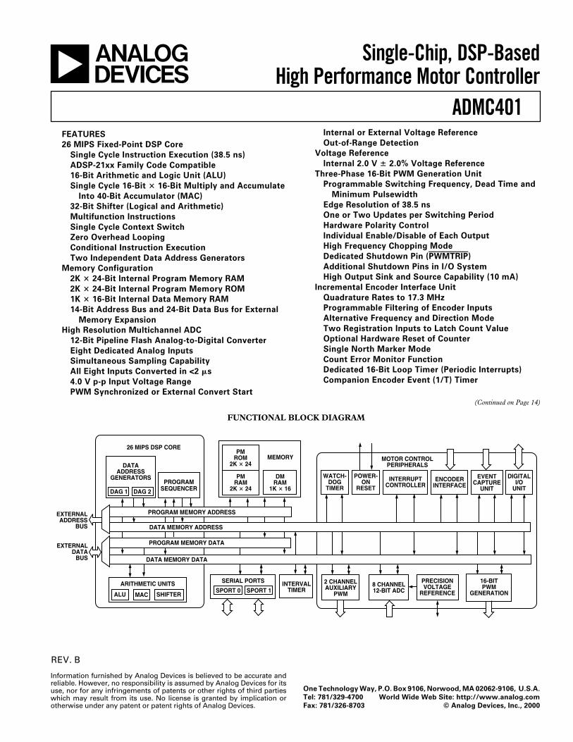
FUNCTIONAL BLOCK DIAGRAM
ARITHMETIC UNITS
SHIFTERMACALU
MEMORY
SPORT 1INTERVAL
TIMER
DMRAM
1K 16
PMROM
2K 24
PMRAM
2K 24
INTERRUPTCONTROLLER
ENCODERINTERFACE
8 CHANNEL12-BIT ADC
26 MIPS DSP CORE
SERIAL PORTS
PROGRAMSEQUENCER
DATAADDRESS
GENERATORS
DAG 1 DAG 2
PROGRAM MEMORY ADDRESS
DATA MEMORY ADDRESS
PROGRAM MEMORY DATA
DATA MEMORY DATA
SPORT 0
WATCH-DOG
TIMER
EVENTCAPTURE
UNIT
DIGITALI/O
UNIT
EXTERNALADDRESS
BUS
EXTERNALDATA
BUS
PRECISIONVOLTAGE
REFERENCE
16-BITPWM
GENERATION
POWER-ON
RESET
MOTOR CONTROLPERIPHERALS
2 CHANNELAUXILIARY
PWM
FEATURES
26 MIPS Fixed-Point DSP Core
Single Cycle Instruction Execution (38.5 ns)
ADSP-21xx Family Code Compatible
16-Bit Arithmetic and Logic Unit (ALU)
Single Cycle 16-Bit 16-Bit Multiply and Accumulate
Into 40-Bit Accumulator (MAC)
32-Bit Shifter (Logical and Arithmetic)
Multifunction Instructions
Single Cycle Context Switch
Zero Overhead Looping
Conditional Instruction Execution
Two Independent Data Address Generators
Memory Configuration
2K 24-Bit Internal Program Memory RAM
2K 24-Bit Internal Program Memory ROM
1K 16-Bit Internal Data Memory RAM
14-Bit Address Bus and 24-Bit Data Bus for External
Memory Expansion
High Resolution Multichannel ADC
12-Bit Pipeline Flash Analog-to-Digital Converter
Eight Dedicated Analog Inputs
Simultaneous Sampling Capability
All Eight Inputs Converted in <2 s
4.0 V p-p Input Voltage Range
PWM Synchronized or External Convert Start
Internal or External Voltage Reference
Out-of-Range Detection
Voltage Reference
Internal 2.0 V 2.0% Voltage Reference
Three-Phase 16-Bit PWM Generation Unit
Programmable Switching Frequency, Dead Time and
Minimum Pulsewidth
Edge Resolution of 38.5 ns
One or Two Updates per Switching Period
Hardware Polarity Control
Individual Enable/Disable of Each Output
High Frequency Chopping Mode
Dedicated Shutdown Pin (PWMTRIP)
Additional Shutdown Pins in I/O System
High Output Sink and Source Capability (10 mA)
Incremental Encoder Interface Unit
Quadrature Rates to 17.3 MHz
Programmable Filtering of Encoder Inputs
Alternative Frequency and Direction Mode
Two Registration Inputs to Latch Count Value
Optional Hardware Reset of Counter
Single North Marker Mode
Count Error Monitor Function
Dedicated 16-Bit Loop Timer (Periodic Interrupts)
Companion Encoder Event (1/T) Timer
(Continued on Page 14)
RECOMMENDED OPERATING CONDITIONSB Grade
Parameter Min Max Unit
VDD Digital Supply Voltage 4.75 5.25 VAVDD Analog Supply Voltage 4.75 5.25 VTAMB Ambient Operating Temperature –40 +85 °C
ELECTRICAL CHARACTERISTICSParameter Test Conditions Min Max Unit
VIH HI-Level Input Voltage1, 2, 3 @ VDD = max 2.0 VVIL LO-Level Input Voltage1, 2, 3 @ VDD = min 0.8 VVOH HI-Level Output Voltage1, 3, 4, 5, 6 @ VDD = min, IOH = –1.0 mA 2.4 V
@ VDD = min, IOH = –0.1 mA VDD – 0.3 VVOL LO-Level Output Voltage1, 3, 4, 5, 6 @ VDD = min, IOL = 2.0 mA 0.4 VVOH HI-Level Output Voltage5 @ VDD = min, IOH = –10.0 mA 2.4 VVOL LO-Level Output Voltage5 @ VDD = min, IOL = 10.0 mA 1.2 VIIH HI-Level Input Current7 @ VDD = max, VIN = VDD max 10 µAIIH HI-Level Input Current8 @ VDD = max, VIN = VDD max 100 µAIIH HI-Level Input Current9 @ VDD = max, VIN = VDD max 10 µAIIL LO-Level Input Current7 @ VDD = max, VIN = 0 V 10 µAIIL LO-Level Input Current8 @ VDD = max, VIN = 0 V 10 µAIIL LO-Level Input Current9 @ VDD = max, VIN = 0 V 100 µAIOZH HI-Level Three-State Leakage Current10 @ VDD = max, VIN = VDD max 10 µAIOZL LO-Level Three-State Leakage Current10 @ VDD = max, VIN = 0 V 10 µAIDD Digital Supply Current (Idle)11 @ VDD = max 40 mAIDD Digital Supply Current (Dynamic)12 @ VDD = max 110 mAIDD Analog Supply Current @ AVDD = max 60 mACI Input Pin Capacitance13 VIN = 2.5 V, fIN = 1 MHz, 8 pF
TAMB = +25°CCO Output Pin Capacitance13, 14 VIN = 2.5 V, fIN = 1 MHz, 8 pF
TAMB = +25°CNOTES1Bidirectional pins: D0–D23, RFS0, RFS1, TFS0, TFS1, SCLK0 and SCLK1, PIO0–PIO11.2Input only pins: PWMTRIP, PWMPOL, PWMSR, RESET, EIA, EIB, EIZ, EIS, ETU0, ETU1, DR1A, DR1B, DR0, CLKIN, CONVST, MMAP, BMODE, BRand PWD.3Programmable I/O Pins (PIO0–PIO11).4Output pins: PWMSYNC, AUX0, AUX1, CLKOUT, DT0, DT1, BG, BGH, PMS, DMS, BMS, RD, WR, PWDACK and A0–A13.5Output pins: AH, AL, BH, BL, CH and CL.6Although specified for TTL outputs, all ADMC401 outputs are CMOS-compatible and will drive to V DD–0.3 V and GND+0.3 V assuming no dc loads.7Input only pins RESET, EIA, EIB, EIZ, EIS, ETU0, ETU1, DR1A, DR1B, DR0, CLKIN, CONVST, MMAP, BMODE, BR and PWD.8Input pins with internal pull-down PIO0–PIO11 and PWMTRIP.9Input pins with internal pull-up, PWMPOL and PWMSR.
10Three-statable pins: A0–A13, D0–D23, PMS, DMS, BMS, RD, WR, DT0, DT1, RFS0, RFS1, TFS0, TFS1, SCLK0, SCLK1.11Idle refers execution of the IDLE instruction. Deasserted pins are driven to V DD or GND. Current reflects device operation with CLKOUT disabled.12Current reflects device operating with no output loads.13Guaranteed but not tested.14Output Pin Capacitance is the capacitive load for any three-state output pin.
Specifications subject to change without notice.
(VDD = AVDD = 5 V 5%, GND = AGND = 0 V, TAMB = –40C to +85C,CLKIN = 13 MHz, unless otherwise noted)
REV. B–2–
ADMC401–SPECIFICATIONS
ANALOG-TO-DIGITAL CONVERTERParameter Test Conditions Min Typ Max Unit
AC SPECIFICATIONSSNR Signal to Noise Ratio fIN = 1.0 kHz 68 70 dBSNRD Signal to Noise and Distortion fIN = 1.0 kHz 66 69 dBTHD Total Harmonic Distortion fIN = 1.0 kHz –76 –70 dBCTLK Channel-Channel Crosstalk fIN = 1.0 kHz –89 –72 dBCMRR Common-Mode Rejection Ratio –90 –72 dBPSRR Power Supply Rejection Ratio 0.025 0.1 % FSR
ACCURACYINL Integral Nonlinearity ±0.6 ±1.5 LSBDNL Differential Nonlinearity ±0.5 ±1.0 LSB
No Missing Codes 12 Bits GuaranteedZero Error 0.1 0.25 % FSRGain Error1 0.4 1.0 % FSR
TEMPERATURE DRIFTZero Error 0.025 % FSRGain Error1 0.025 % FSR
INPUT VOLTAGEVIN Voltage Span 4.0 V p-pCIN Input Capacitance2 10 pF
CONVERSION TIMEtCONV Total Conversion Time All 8 Channels 1.88 µs
NOTES1Excludes Internal Voltage Reference Error.2Analog Input Pins VIN0 to VIN7.
Typical values are neither tested nor guaranteed.Specifications subject to change without notice.
VOLTAGE REFERENCEParameter Test Conditions Min Typ Max Unit
VREF Output Voltage Reference SENSE = REFCOM 1.96 2.0 2.04 VOutput Voltage Tolerance1 SENSE = REFCOM 6 mVOutput Current 1.0 mALoad Regulation 1.0 mA Load Current 0.3 1.5 mVPower Supply Rejection Ratio 0.1 1.5 mVReference Input Resistance 8 kΩ
NOTES1Relative tolerance due to temperature change, TMIN to TMAX.
Specifications subject to change without notice.
POWER-ON RESETParameter Test Conditions Min Typ Max Unit
VRST Reset Threshold Voltage 3.25 4.0 VVHYST Hysteresis Voltage 75 mV
Specifications subject to change without notice.
(VDD = AVDD = 5 V 5%, GND = AGND = 0 V, TAMB = –40C to +85C, CLKIN = 13 MHz,VIN0 to VIN7 = 4.0 V p-p, VREF = 2.0 V, unless otherwise noted)
(VDD = AVDD = 5 V 5%, GND = AGND = 0 V, TAMB = –40C to +85C, CLKIN = 13 MHz, VIN0 to VIN7 =4.0 V p-p, VREF = 2.0 V, unless otherwise noted)
(GND = AGND = 0 V, TAMB = –40C to +85C, CLKIN = 13 MHz, unless otherwise noted)
ADMC401
–3–REV. B
REV. B
ADMC401
–4–
ABSOLUTE MAXIMUM RATINGS*Supply Voltage . . . . . . . . . . . . . . . . . . . . . . . . . . –0.3 V to +7 VInput Voltage . . . . . . . . . . . . . . . . . . . . . –0.3 V to VDD + 0.3 VOutput Voltage Swing . . . . . . . . . . . . . . –0.3 V to VDD + 0.3 VOperating Temperature Range (Ambient) . . . . –40°C to +85°CStorage Temperature Range . . . . . . . . . . . . . –65°C to +150°CLead Temperature (5 sec) . . . . . . . . . . . . . . . . . . . . . . +280°C*Stresses above those listed under absolute maximum ratings may cause permanent
damage to the device. These are stresses only; functional operation of the deviceat these or any other conditions above those indicated in the operational section ofthis specification is not implied. Exposure to absolute maximum rating conditionsfor extended periods may affect device reliability.
CAUTIONESD (electrostatic discharge) sensitive device. Electrostatic charges as high as 4000 V readilyaccumulate on the human body and test equipment and can discharge without detection.Although the ADMC401 features proprietary ESD protection circuitry, permanent damage mayoccur on devices subjected to high-energy electrostatic discharges. Therefore, proper ESDprecautions are recommended to avoid performance degradation or loss of functionality.
WARNING!
ESD SENSITIVE DEVICE
ORDERING GUIDE
Temperature Instruction Package PackageModel Range Rate Description Option
ADMC401BST –40°C to +85°C 26 MHz 144-Lead Plastic Thin Quad Flatpack (LQFP) ST-144ADMC401-ADVEVALKIT Development Tool KitADMC401-PB Evaluation/Processor Board
Timing ParametersGENERAL NOTESUse the exact timing information given. Do not attempt toderive parameters from the addition or subtraction of others.While addition or subtraction would yield meaningful results foran individual device, the values given in this data sheet reflectstatistical variations and worst cases. Consequently, you cannotmeaningfully add up parameters to derive longer times.
TIMING NOTESSwitching characteristics specify how the processor changes itssignals. You have no control over this timing; it is dependent onthe internal design. Timing requirements apply to signals thatare controlled outside the processor, such as the data input for aread operation.
Timing requirements guarantee that the processor operatescorrectly with another device. Switching characteristics tell youwhat the device will do under a given circumstance. Also, usethe switching characteristics to ensure any timing requirementof a device connected to the processor (such as memory) issatisfied.
MEMORY REQUIREMENTSThis chart links common memory device specification namesand ADMC401 timing parameters for your convenience.
CommonParameter Memory DeviceName Function Specification Name
tASW A0–A13, DMS, PMS Address Setup toSetup before WR Low Write Start
tAW A0–A13, DMS, PMS Address Setup tobefore WR Deasserted Write End
tWRA A0–A13, DMS, PMS Address Hold TimeHold after WR Deasserted
tDW Data Setup before WR High Data Setup TimetDH Data Hold after WR High Data Hold TimetRDD RD Low to Data Valid OE to Data ValidtAA A0–A13, DMS, PMS, Address Access Time
BMS to Data Valid
ADMC401
–5–REV. B
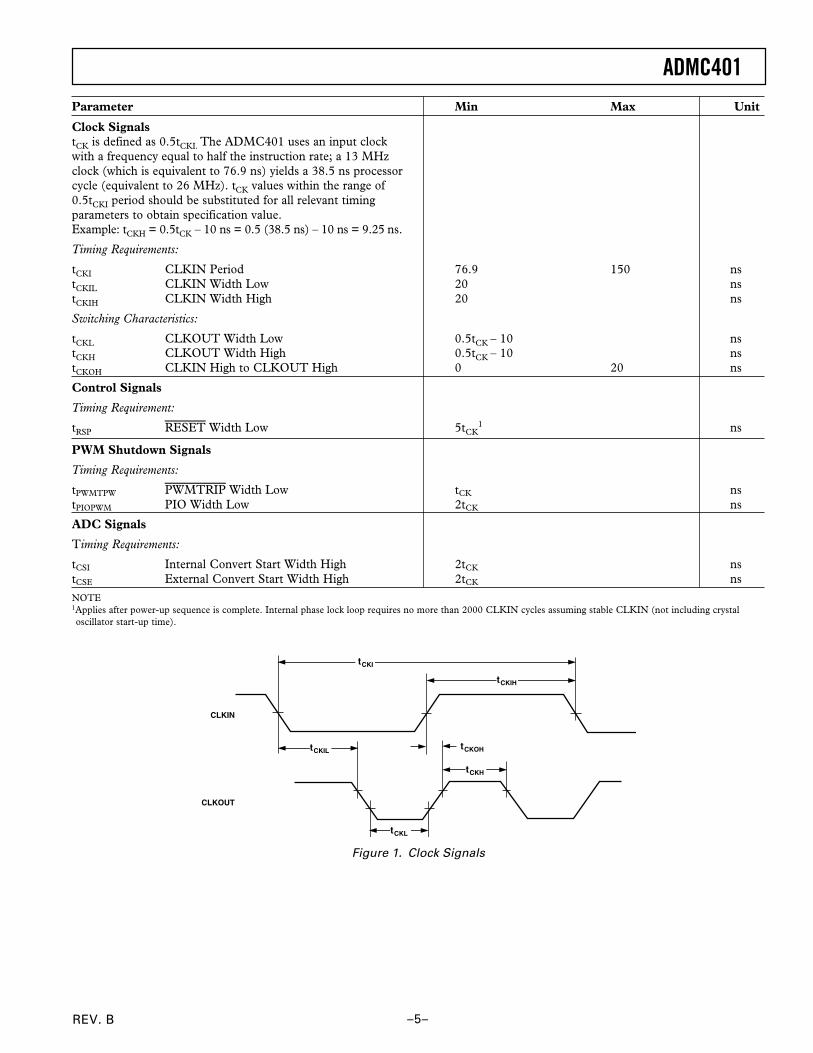
Parameter Min Max Unit
Clock SignalstCK is defined as 0.5tCKI. The ADMC401 uses an input clockwith a frequency equal to half the instruction rate; a 13 MHzclock (which is equivalent to 76.9 ns) yields a 38.5 ns processorcycle (equivalent to 26 MHz). tCK values within the range of0.5tCKI period should be substituted for all relevant timingparameters to obtain specification value.Example: tCKH = 0.5tCK – 10 ns = 0.5 (38.5 ns) – 10 ns = 9.25 ns.
Timing Requirements:
tCKI CLKIN Period 76.9 150 nstCKIL CLKIN Width Low 20 nstCKIH CLKIN Width High 20 ns
Switching Characteristics:
tCKL CLKOUT Width Low 0.5tCK – 10 nstCKH CLKOUT Width High 0.5tCK – 10 nstCKOH CLKIN High to CLKOUT High 0 20 ns
Control Signals
Timing Requirement:
tRSP RESET Width Low 5tCK1 ns
PWM Shutdown Signals
Timing Requirements:
tPWMTPW PWMTRIP Width Low tCK nstPIOPWM PIO Width Low 2tCK ns
ADC Signals
Timing Requirements:
tCSI Internal Convert Start Width High 2tCK nstCSE External Convert Start Width High 2tCK nsNOTE1Applies after power-up sequence is complete. Internal phase lock loop requires no more than 2000 CLKIN cycles assuming stable CLKIN (not including crystaloscillator start-up time).
CLKIN
CLKOUT
tCKOH
tCKI
tCKIH
tCKIL
tCKH
tCKL
Figure 1. Clock Signals
REV. B
ADMC401
–6–
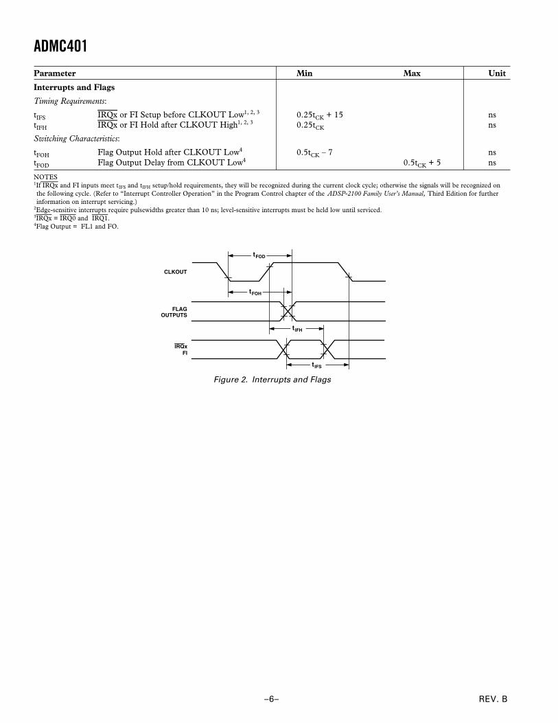
Parameter Min Max Unit
Interrupts and Flags
Timing Requirements:
tIFS IRQx or FI Setup before CLKOUT Low1, 2, 3 0.25tCK + 15 nstIFH IRQx or FI Hold after CLKOUT High1, 2, 3 0.25tCK ns
Switching Characteristics:
tFOH Flag Output Hold after CLKOUT Low4 0.5tCK – 7 nstFOD Flag Output Delay from CLKOUT Low4 0.5tCK + 5 ns
NOTES1If IRQx and FI inputs meet tIFS and tIFH setup/hold requirements, they will be recognized during the current clock cycle; otherwise the signals will be recognized onthe following cycle. (Refer to “Interrupt Controller Operation” in the Program Control chapter of the ADSP-2100 Family User’s Manual, Third Edition for furtherinformation on interrupt servicing.)
2Edge-sensitive interrupts require pulsewidths greater than 10 ns; level-sensitive interrupts must be held low until serviced.3IRQx = IRQ0 and IRQ1.4Flag Output = FL1 and FO.
CLKOUT
FLAGOUTPUTS
IRQxFI
tFOH
tIFH
tIFS
tFOD
Figure 2. Interrupts and Flags
ADMC401
–7–REV. B
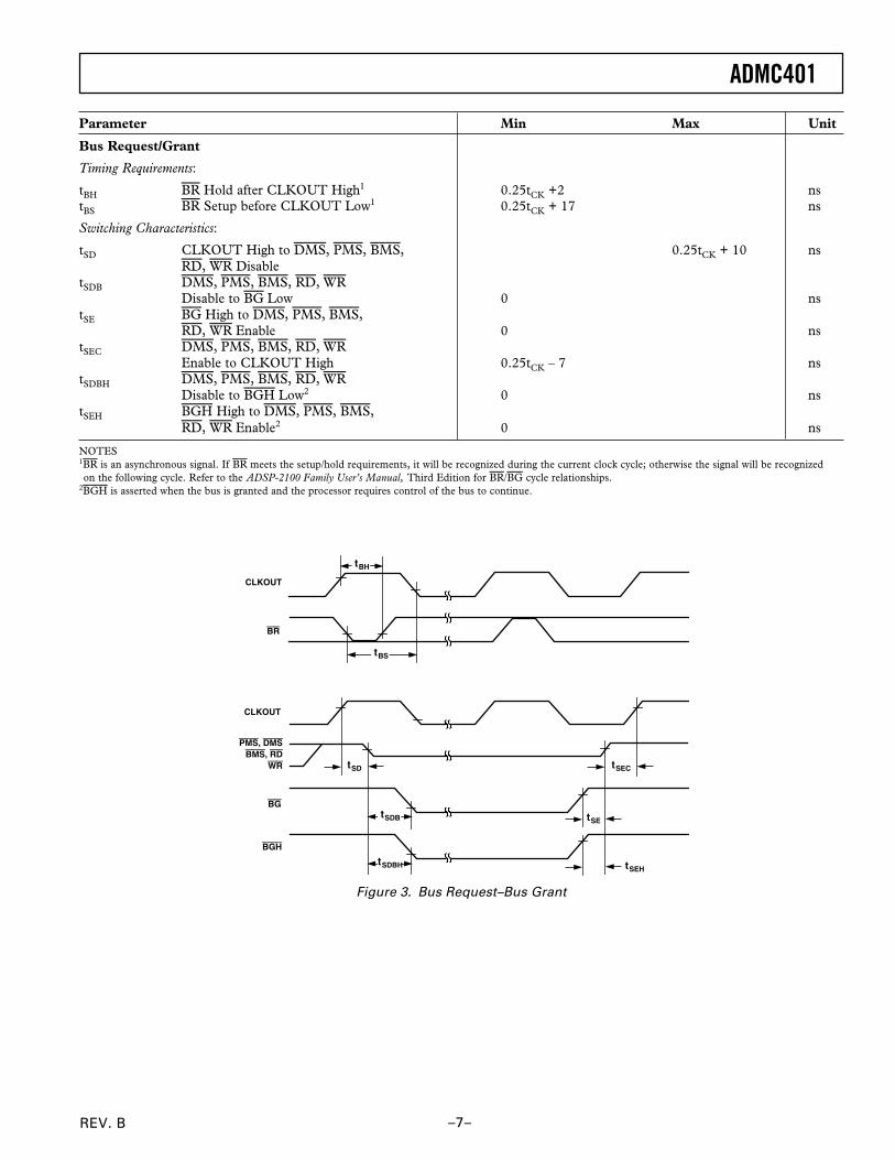
Parameter Min Max Unit
Bus Request/Grant
Timing Requirements:
tBH BR Hold after CLKOUT High1 0.25tCK +2 nstBS BR Setup before CLKOUT Low1 0.25tCK + 17 ns
Switching Characteristics:
tSD CLKOUT High to DMS, PMS, BMS, 0.25tCK + 10 nsRD, WR Disable
tSDB DMS, PMS, BMS, RD, WRDisable to BG Low 0 ns
tSE BG High to DMS, PMS, BMS,RD, WR Enable 0 ns
tSEC DMS, PMS, BMS, RD, WREnable to CLKOUT High 0.25tCK – 7 ns
tSDBH DMS, PMS, BMS, RD, WRDisable to BGH Low2 0 ns
tSEH BGH High to DMS, PMS, BMS,RD, WR Enable2 0 ns
NOTES1BR is an asynchronous signal. If BR meets the setup/hold requirements, it will be recognized during the current clock cycle; otherwise the signal will be recognizedon the following cycle. Refer to the ADSP-2100 Family User’s Manual, Third Edition for BR/BG cycle relationships.
2BGH is asserted when the bus is granted and the processor requires control of the bus to continue.
BR
CLKOUT
PMS, DMSBMS, RD
WR
BG
CLKOUT
BGH
tBH
tBS
tSD
tSDB
tSDBH tSEH
tSE
tSEC
Figure 3. Bus Request–Bus Grant
REV. B
ADMC401
–8–
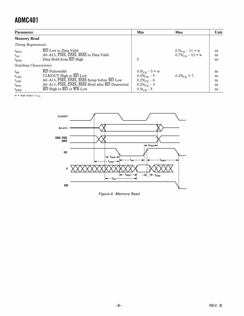
Parameter Min Max Unit
Memory Read
Timing Requirements:
tRDD RD Low to Data Valid 0.5tCK – 11 + w nstAA A0–A13, PMS, DMS, BMS to Data Valid 0.75tCK – 12 + w nstRDH Data Hold from RD High 0 ns
Switching Characteristics:
tRP RD Pulsewidth 0.5tCK – 5 + w nstCRD CLKOUT High to RD Low 0.25tCK – 5 0.25tCK + 7 nstASR A0–A13, PMS, DMS, BMS Setup before RD Low 0.25tCK – 6 nstRDA A0–A13, PMS, DMS, BMS Hold after RD Deasserted 0.25tCK – 3 nstRWR RD High to RD or WR Low 0.5tCK – 5 ns
w = wait states × tCK.
CLKOUT
A0–A13
D
RD
WR
DMS, PMSBMS
tRWR tRP
tASR
tCRD
tAA
tRDA
tRDD tRDH
Figure 4. Memory Read
ADMC401
–9–REV. B
Parameter Min Max Unit
Memory Write
Switching Characteristics:
tDW Data Setup before WR High 0.5tCK – 7 + w nstDH Data Hold after WR High 0.25tCK – 2 nstWP WR Pulsewidth 0.5tCK – 5 + w nstWDE WR Low to Data Enabled 0 nstASW A0–A13, DMS, PMS Setup before WR Low 0.25tCK – 6 nstDDR Data Disable before WR or RD Low 0.25tCK – 6 nstCWR CLKOUT High to WR Low 0.25tCK – 5 0.25tCK + 7 nstAW A0–A13, DMS, PMS, Setup before WR Deasserted 0.75tCK – 9 + w nstWRA A0–A13, DMS, PMS Hold after WR Deasserted 0.25tCK – 3 nstWWR WR High to RD or WR Low 0.5tCK – 5 ns
w = wait states × tCK.
CLKOUT
A0–A13
D
WR
DMS, PMS
RD
tWRA
tWWR tWP tASW
tAW tDH tDDR tCWR
tWDE
tDW
Figure 5. Memory Write
REV. B
ADMC401
–10–
Parameter Min Max Unit
Serial Ports
Timing Requirements:
tSCK SCLK Period 50 nstSCS DR/TFS/RFS Setup before SCLK Low 5 nstSCH DR/TFS/RFS Hold after SCLK Low 10 nstSCP SCLKIN Width 20 ns
Switching Characteristics:
tCC CLKOUT High to SCLKOUT 0.25tCK 0.25tCK + 15 nstSCDE SCLK High to DT Enable 0 nstSCDV SCLK High to DT Valid 20 nstRH TFS/RFSOUT Hold after SCLK High 0 nstRD TFS/RFSOUT Delay from SCLK High 20 nstSCDH DT Hold after SCLK High 0 nstTDE TFS(Alt) to DT Enable 0 nstTDV TFS(Alt) to DT Valid 20 nstSCDD SCLK High to DT Disable 20 nstRDV RFS (Multichannel, Frame Delay Zero) to DT Valid 20 ns
CLKOUT
SCLK
TFS
RFS
DRRFSINTFSIN
DT
alternateframe mode
RFSOUTTFSOUT
multichannel mode,frame delay 0
(MFD = 0)
tCC tCC
tSCS tSCS
tSCK
tSCP
tSCP
tRD
tRH
tSCDV
tSCDE
tTDE
tTDV
tRDV
tSCDH
tSCDD
Figure 6. Serial Ports
ADMC401
–11–REV. B
POWER DISSIPATIONTo determine total power dissipation in a specific application,the following equation should be applied for each output:
C × VDD2 × f
C = load capacitance, f = output switching frequency.
Example:In an application where external data memory is used and noother outputs are active, power dissipation is calculated asfollows:
Assumptions:
• External data memory is accessed every cycle with 50% of theaddress pins switching.
• External data memory writes occur every other cycle with50% of the data pins switching.
• Each address and data pin has a 10 pF total load at the pin.
• The application operates at VDD = 5.0 V and tCK = 38.5 ns.
Total Power Dissipation = PINT + (C × VDD2 × f)
PINT = VDD × (IDD Digital + IDD Analog)
(C × VDD2 × f) is calculated for each output:
# ofPins C VDD
2 f
Address, DMS 8 × 10 pF × 52 V × 26 MHz = 52.00 mWData Output, WR 9 × 10 pF × 52 V × 13 MHz = 29.25 mWRD 1 × 10 pF × 52 V × 13 MHz = 3.25 mWCLKOUT 1 × 10 pF × 52 V × 26 MHz = 6.50 mW
91.00 mW
Total power dissipation for this example is PINT + 91 mW.
TEST CONDITIONSOutput Disable TimeOutput pins are considered to be disabled when they havestopped driving and started a transition from the measuredoutput high or low voltage to a high impedance state. The out-put disable time (tDIS) is the difference of tMEASURED and tDECAY,as shown in the Output Enable/Disable diagram. The time is theinterval from when a reference signal reaches a high or lowvoltage level to when the output voltages have changed by 0.5 Vfrom the measured output high or low voltage. The decay time,tDECAY, is dependent on the capacitative load, CL, and the cur-rent load, iL, on the output pin. It can be approximated by thefollowing equation:
t
C VIDECAY
L
L=
× 0 5.
from which
t t tDIS MEASURED DECAY= −is calculated. If multiple pins (such as the data bus) are dis-abled, the measurement value is that of the last pin to stopdriving.
3.0V1.5V
0.0V
2.0V1.5V
0.3V
INPUT
OUTPUT
Figure 7. Voltage Reference Levels for AC Measure-ments (Except Output Enable/Disable)
Output Enable TimeOutput pins are considered to be enabled when that have madea transition from a high-impedance state to when they startdriving. The output enable time (tENA) is the interval from whena reference signal reaches a high or low voltage level to whenthe output has reached a specified high or low trip point, asshown in the Output Enable/Disable diagram. If multiple pins(such as the data bus) are enabled, the measurement value isthat of the first pin to start driving.
2.0V
1.0V
tENA
REFERENCESIGNAL
OUTPUT
tDECAY
VOH(MEASURED)
OUTPUT STOPSDRIVING
OUTPUT STARTSDRIVING
tDIS
tMEASURED
VOL(MEASURED)
VOH (MEASURED) – 0.5V
VOL (MEASURED) +0.5V
HIGH-IMPEDANCE STATE. TEST CONDITIONS CAUSETHIS VOLTAGE LEVEL TO BE APPROXIMATELY 1.5V.
VOH(MEASURED)
VOL(MEASURED)
Figure 8. Output Enable/Disable
TOOUTPUT
PIN50pF
+1.5V
IOH
IOL
Figure 9. Equivalent Device Loading for AC Measure-ments (Including All Fixtures)
REV. B
ADMC401
–12–
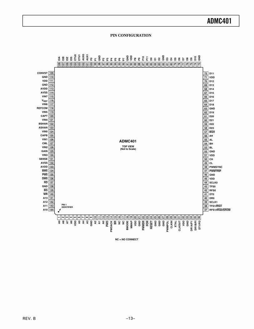
PIN FUNCTION DESCRIPTION
Pin Pin Pin Pin Pin Pin Pin PinNo. Name No. Name No. Name No. Name
1 A9 37 RFS1/IRQ0/SROM 73 GND 109 CONVST2 A8 38 TFS1/IRQ1 74 D10 110 GND3 A7 39 SCLK1 75 D9 111 VDD4 A6 40 DR0 76 D8 112 GND5 VDD 41 DT0 77 D7 113 AVDD6 A5 42 RFS0 78 D6 114 AVSS7 A4 43 TFS0 79 D5 115 VIN78 A3 44 SCLK0 80 D4 116 VREF
9 GND 45 VDD 81 D3 117 VIN610 A2 46 GND 82 GND 118 REFCOM11 A1 47 PWMTRIP 83 D2 119 VIN512 A0 48 PWMSYNC 84 D1 120 CAPT13 PWD 49 CL 85 D0 121 VIN414 PWDACK 50 CH 86 P11 122 BSHAN15 BR 51 VDD 87 P10 123 ASHAN16 NC 52 GND 88 P9 124 VIN017 NC 53 BL 89 P8 125 CAPB18 BMODE 54 BH 90 VDD 126 VIN119 MMAP 55 AL 91 GND 127 CML20 VDD 56 AH 92 P7 128 VIN221 GND 57 BGH 93 P6 129 GAIN22 PWMSR 58 D23 94 P5 130 VIN323 POR 59 D22 95 P4 131 SENSE24 RESET 60 D21 96 P3 132 AVSS25 GND 61 D20 97 P2 133 AVDD26 GND 62 D19 98 GND 134 BMS27 GND 63 GND 99 P1 135 PMS28 PWMPOL 64 D18 100 P0 136 DMS29 CLKIN 65 D17 101 AUX1 137 RD30 XTAL 66 D16 102 AUX0 138 GND31 CLKOUT 67 D15 103 ETU1 139 BG32 VDD 68 D14 104 ETU0 140 WR33 GND 69 D13 105 EIS 141 A1334 DR1A/FI 70 D12 106 EIZ 142 A1235 DRIB/FI 71 VDD 107 EIB 143 A1136 DT1/FO 72 D11 108 EIA 144 A10
NC: These pins must be left unconnected
ADMC401
–13–REV. B
PIN CONFIGURATION
A9
A8
A7
A6
VD
D A5
A4
A3
GN
D
A2
A1
A0
PW
D
PW
DA
CK
BR
NC
NC
BM
OD
E
MM
AP
VD
D
GN
D
PW
MS
R
PO
R
RE
SE
T
GN
D
GN
D
GN
D
PW
MP
OL
CL
KIN
XT
AL
CL
KO
UT
VD
D
GN
D
DR
1A/F
1
DR
1B/F
I
DT
1/F
O
P1
GN
D
P2
P3
P4
P5
P6
P7
GN
DV
DD
P8
P9
P10
P11
D0
D1
D2
GN
D
D3
D4
D5
D6
D7
D8
D9
D10
GN
D
EIA
EIB
EIZ
EIS
ET
U0
ET
U1
AU
X0
AU
X1
P0
D11
VDD
D12
D13
D14
D15
D16
D17
D18
GND
D19
D20
D21
D22
D23
BGH
AH
AL
BH
BL
GND
VDD
CH
CL
PWMSYNC
PWMTRIP
GND
VDD
SCLK0
TFS0
RFS0
DT0
DR0
SCLK1
TFS1/IRQ1
RFS1/IRQ0/SROM
CONVST
GND
VDD
GND
AVDD
AVSS
VIN7
VREF
VIN6
REFCOM
VIN5
CAPT
VIN4
BSHAN
ASHAN
VIN0
CAPB
VIN1
CML
VIN2
GAIN
VIN3
SENSE
AVSS
AVDD
BMS
PMS
DMS
RD
GND
BG
WR
A13
A12
A11
A10
NC = NO CONNECT
PIN 1IDENTIFIER
TOP VIEW(Not to Scale)
ADMC401
19 20 21 22 23 24 25 26 27 28 29 30 31 32 33 34 35 3610 11 12 13 14 15 16 17 181 2 3 4 5 6 7 8 9
90 89 88 87 86 85 84 83 82 81 80 79 78 77 76 75 74 7399 98 97 96 95 94 93 92 91108
107
106
105
104
103
102
101
100
72
71
70
69
68
67
66
65
64
63
62
61
60
59
58
57
56
55
54
53
52
51
50
49
48
47
46
45
44
43
42
41
40
39
38
37
109
110
111
112
113
114
115
116
117
118
119
120
121
122
123
124
125
126
127
128
129
130
131
132
133
134
135
136
137
138
139
140
141
142
143
144
REV. B
ADMC401
–14–
(Continued from Page 1)
Programmable Digital I/O (PIO) Port
12-Pin Configurable Digital I/O Port
Flexible Interrupt Generation
Four Dedicated PIO Interrupt Vectors
Each I/O Line Configurable as PWM Shutdown
Two 8-Bit Auxiliary PWM Outputs
Programmable Switching Frequency
Independent or Offset Modes
Two-Channel Event Timer (Capture) Unit
Configurable Event Definition
Single-Shot or Free-Running Modes
Peripheral Interrupt Controller
Manages Peripheral Interrupts
16-Bit Watchdog Timer
Internal Power-On Reset System
Programmable 16-Bit Interval Timer with Prescaler
Two Double Buffered Synchronous Serial Ports
Boot Load Protocols via SPORT1:
Synchronous E2PROM/SROM Booting
UART Boot Loader with Autobaud
Synchronous Master or Slave Boot Loader
Debugger Interface via SPORT1:
UART Interface with Autobaud
Synchronous Master or Slave Interface
Full Debugger for Program Development
Industrial Temperature Range –40C to +85COperating Voltage 5.0 V 5%
Package: 144-Lead LQFP
GENERAL DESCRIPTIONThe ADMC401 is a single-chip DSP-based controller, suitablefor high performance control of ac induction motors (ACIM),permanent magnet synchronous motors (PMSM), brushless dcmotors (BDCM) and switched reluctance (SR) motors in indus-trial applications. The ADMC401 integrates a 26 MIPS, fixed-point DSP core with a complete set of motor control peripheralsthat permits fast motor control in a highly integrated environment.
The DSP core of the ADMC401 is the ADSP-2171 which iscompletely code compatible with the ADSP-21xx DSP family(as well as other members of the integrated motor controllers ofthe ADMC3xx family) and combines three computational units,
data address generators and a program sequencer. The computa-tional units comprise an ALU, a multiplier/accumulator (MAC)and a barrel shifter. The DSP core also adds instructions for bitmanipulation, squaring (x2), biased rounding and global inter-rupt masking. In addition, two flexible double-buffered, bidirec-tional synchronous serial ports are included in the ADMC401.
The ADMC401 provides 2K × 24-bit internal program memoryRAM, 2K × 24-bit internal program memory ROM and 1K ×16-bit internal data memory RAM. The program and datamemory RAM can be boot loaded through the serial port fromeither a serial E2PROM, through a UART connection (eitherfrom external host microprocessor or from the Motion ControlDebugger) or via a synchronous serial interface from a hostmicroprocessor. Alternatively, the internal program and datamemory RAM may be booted from an external device across theaddress and data buses. The program memory ROM includes amonitor that adds software debugging features through the serialport.
Additionally, the ADMC401 device adds significant externalmemory and peripheral expansion capabilities by making avail-able the full address and data bus of the DSP core. This featurepermits expansion of both external program and data memoryand means that the DSP core can address up to 14K × 24 bits ofexternal program memory and up to 13K × 16 bits of externaldata memory.
The ADMC401 contains a number of special purpose, motorcontrol peripherals. The first is a high performance, 8-channel,12-bit ADC system with dual channel simultaneous samplingability across 4 pair of inputs. An internal precision voltage refer-ence is also available as part of the ADC system. In addition, athree-phase, 16-bit, center-based PWM generation unit can beused to produce high-accuracy PWM signals with minimal pro-cessor overhead. The ADMC401 also contains a flexible incre-mental encoder interface unit for position sensor feedback;two adjustable-frequency auxiliary PWM outputs, 12 lines ofdigital I/O; a 2-channel event capture system; a 16-bit watchdogtimer; two 16-bit interval timers (one of which can be linked tothe encoder interface unit) and an interrupt controller that man-ages all peripheral interrupts. Finally, the ADMC401 containsan integrated power-on-reset (POR) circuit that can be used togenerate the required reset signal for the device on power-on.
ADMC401
–15–REV. B
BUSEXCHANGE
DATAADDRESS
GENERATOR#2
DATAADDRESS
GENERATOR#1
14
14
24
16
6R BUS
16
COMPANDINGCIRCUITRY
DMA BUS
PMA BUS
DMD BUS
PMD BUS
PROGRAMSEQUENCER
INSTRUCTIONREGISTER
INPUT REGS
OUTPUT REGS
SHIFTER
INPUT REGS
OUTPUT REGS
MAC
INPUT REGS
OUTPUT REGS
ALU
SERIALPORT 0
RECEIVE REG
TRANSMIT REG
CONTROLLOGIC
DM RAM1K 16
PM ROM2K 24
PM RAM2K 24
SERIALPORT 1
RECEIVE REG
TRANSMIT REG
5
TIMER
BOOTADDRESS
GENERATOR
14
24
2POWER DOWNCONTROL
LOGIC
EXTERNALDATA BUS
EXTERNALADDRESS BUS
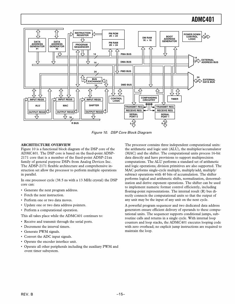
Figure 10. DSP Core Block Diagram
ARCHITECTURE OVERVIEWFigure 10 is a functional block diagram of the DSP core of theADMC401. The DSP core is based on the fixed-point ADSP-2171 core that is a member of the fixed-point ADSP-21xxfamily of general purpose DSPs from Analog Devices Inc.The ADSP-2171 flexible architecture and comprehensive in-struction set allow the processor to perform multiple operationsin parallel.
In one processor cycle (38.5 ns with a 13 MHz crystal) the DSPcore can:
• Generate the next program address.• Fetch the next instruction.• Perform one or two data moves.• Update one or two data address pointers.• Perform a computational operation.
This all takes place while the ADMC401 continues to:
• Receive and transmit through the serial ports.• Decrement the interval timers.• Generate PWM signals.• Convert the ADC input signals.• Operate the encoder interface unit.• Operate all other peripherals including the auxiliary PWM and
event timer subsystem.
The processor contains three independent computational units:the arithmetic and logic unit (ALU), the multiplier/accumulator(MAC) and the shifter. The computational units process 16-bitdata directly and have provisions to support multiprecisioncomputations. The ALU performs a standard set of arithmeticand logic operations; division primitives are also supported. TheMAC performs single-cycle multiply, multiply/add, multiply/subtract operations with 40 bits of accumulation. The shifterperforms logical and arithmetic shifts, normalization, denormal-ization and derive exponent operations. The shifter can be usedto implement numeric format control efficiently, includingfloating-point representations. The internal result (R) bus di-rectly connects the computational units so that the output ofany unit may be the input of any unit on the next cycle.
A powerful program sequencer and two dedicated data addressgenerators ensure efficient delivery of operands to these compu-tational units. The sequencer supports conditional jumps, sub-routine calls and returns in a single cycle. With internal loopcounters and loop stacks, the ADMC401 executes looping codewith zero overhead; no explicit jump instructions are required tomaintain the loop.
REV. B
ADMC401
–16–
Two data address generators (DAGs) provide addresses forsimultaneous dual operand fetches from data memory and pro-gram memory. Each DAG maintains and updates four addresspointers (I registers). Whenever the pointer is used to accessdata (indirect addressing), it is post-modified by the value inone of four modify (M) registers. A length value may be associ-ated with each pointer (L registers) to implement automaticmodulo addressing for circular buffers. The circular bufferingfeature is also used by the serial ports for automatic data trans-fers to and from on-chip memory. DAG1 generates only datamemory addresses but provides an optional bit-reversal capabil-ity. DAG2 may generate either program or data memory ad-dresses, but has no bit-reversal capability.
Efficient data transfer is achieved with the use of five internalbuses:
• Program Memory Address (PMA) Bus.• Program Memory Data (PMD) Bus.• Data Memory Address (DMA) Bus.• Data Memory Data (DMD) Bus.• Result (R) Bus.
Program memory can store both instructions and data, permit-ting the ADMC401 to fetch two operands in a single cycle, onefrom internal program memory and one from internal datamemory. The ADMC401 can fetch an operand from on-chipprogram memory and the next instruction in the same cycle.
The ADMC401 writes data from its 16-bit registers to the 24-bit program memory using the PX register to provide the lowereight bits. When it reads data (not instructions) from 24-bitprogram memory to a 16-bit data register, the lower eight bitsare placed in the PX register.
The ADMC401 can respond to a number of distinct DSP coreand peripheral interrupts. The DSP core interrupts includeserial port receive and transmit interrupts, timer interrupts,software interrupts and external interrupts. In addition, there isa master RESET signal. The motor control peripherals alsoproduce interrupts to the DSP core.
The two serial ports (SPORTs) provide a complete synchronousserial interface with optional companding in hardware and awide variety of framed and unframed data transmit and receivemodes of operation. Each SPORT can generate an internalprogrammable serial clock or accept an external serial clock.
Boot loading of both the program and data memory RAM of theADMC401 can be through the serial port SPORT1. Alterna-tively the ADMC401 can be boot loaded from an external byte-wide memory connected to the external address and data buses.After reset, seven wait states are automatically generated. Thispermits, for example, a 38.5 ns ADMC401 to use an external250 ns EPROM as boot memory. The internal boot addressgenerator provides the addresses for booting from an externalbyte-wide memory.
A programmable interval counter is also included in the DSPcore and can be used to generate periodic interrupts. A 16-bitcount register (TCOUNT) is decremented every n processorcycles, where n-1 is a scaling value stored in the 8-bit TSCALE
register. When the value of the counter reaches zero, an inter-rupt is generated and the count register is reloaded from a 16-bit period register (TPERIOD).
The ADMC401 instruction set provides flexible data moves andmultifunction (one or two data moves with a computation)instructions. Each instruction is executed in a single 38.5 nsprocessor cycle (for a 13 MHz crystal). The ADMC401 assem-bly language uses an algebraic syntax for ease of coding andreadability. A comprehensive set of development tools supportsprogram development.
Serial PortsThe ADMC401 incorporates two complete synchronous serialports (SPORT0 and SPORT1) for serial communications andmultiprocessor communication. The following is a brief list ofthe capabilities of the ADMC401 SPORTs. Refer to the ADSP-2100 Family User’s Manual, Third Edition for further details.
• SPORTs are bidirectional and have a separate, double- buffered transmit and receive section.
• SPORTs can use an external serial clock or generate theirown serial clock internally.
• SPORTs have independent framing for the receive and trans-mit sections. Sections run in a frameless mode or with framesynchronization signals internally or externally generated.Frame synchronization signals are active high or inverted,with either of two pulsewidths and timings.SPORTs support serial data word lengths from 3 bits to 16bits and provide optional A-law and µ-law companding.
• SPORT receive and transmit sections can generate uniqueinterrupts on completing a data word transfer.
• SPORTs can receive and transmit an entire circular buffer ofdata with only one overhead cycle per data word. An inter-rupt is generated after a data buffer transfer.
• SPORT0 has a multichannel interface to selectively receiveand transmit a 24-word or 32-word, time-division multi-plexed, serial bitstream.
• SPORT1 can be configured to have two external interrupts(IRQ0 and IRQ1), and the Flag In and Flag Out signals. Theinternally generated serial clock may still be used in thisconfiguration.
The following are additional capabilities of the ADMC401SPORTs that are not part of the ADSP-21xx products:• SPORT1 is the input for single pin program and data
memory boot loading. The RFS1 pin can be configuredinternally to the ADMC401 as an SROM/E2PROM resetsignal.
• SPORT1 has two data receive pins (DR1A and DR1B). TheDR1A pin is intended only for synchronous data receivefrom the external E2PROM. The DR1B pin can be used asthe data receive pin for a general purpose SPORT after boot-ing or as the data receive pin for other boot load modes or asthe UART/debugger interface. The DR1A and DR1B pinsare internally multiplexed onto the one data receive pin ofthe SPORT. The particular data receive pin selected is deter-mined by Bit 4 of the MODECTRL register.
ADMC401
–17–REV. B
PIN FUNCTION DESCRIPTIONThe ADMC401 is available in an 144-lead TQFP package. TableI contains the pin descriptions.
Table I. Pin List
Pin #Group of Input/Name Pins Output Function
A13–A0 14 O Address Lines
D23–D0 24 I/O Data Lines
PMS, DMS, BMS 3 O External Memory Select Lines
RD, WR 2 O External Memory Read/Write Enable
MMAP 1 I Memory Map Select
POR 1 O Internal Power On Reset Output
RESET 1 I Processor Reset Input
CLKOUT 1 O Processor Clock Output
CLKIN, XTAL 2 I, O External Clock or Quartz CrystalInput
BR 1 I Bus Request
BG, BGH 2 O Bus Grant and Bus Hang Control
BMODE 1 I Boot Mode Select
PWD, PWDACK 2 I, O Power-Down and Power-DownAcknowledge
SPORT0 5 I/O Serial Port 0 Pins (TFS0, RFS0,DT0, DR0, SCLK0)
SPORT1 6 I/O Serial Port 1 (TFS1/IRQ1, RFS1/IRQ0/SROM, DT1/FO, DR1A/FI,DR1B/FI, SCLK1)
VIN0–VIN7 8 I Analog Inputs
ASHAN, BSHAN 2 I Inverting Inputs to Sample andHold Amplifiers
GAIN 1 I Analog Input for Gain Calibration
VREF 1 I/O Reference Voltage Input/Output
REFCOM 1 GND Reference Common
CML 1 O Common-Mode Level (Midsupply)
CAPT, CAPB 2 O Noise Reduction Pins
SENSE 1 I Voltage Reference Select
CONVST 1 I External Convert Start
AH-CL 6 O PWM Outputs
PWMTRIP 1 I PWM Shutdown Signal
PWMPOL 1 I PWM Polarity Control
PWMSYNC 1 O PWM Synchronization Output
PWMSR 1 I PWM Switched Reluctance ModeControl
PIO0–PIO11 12 I/O Digital I/O Port
ETU0, ETU1 2 I Event Timer Inputs
AUX0–AUX1 2 O Auxiliary PWM Outputs
EIA, EIB, EIZ,EIS 4 I Encoder Interface Inputs and
External Registration Inputs
NC 2 No Connect
AVDD 2 SUP Analog Power Supply
AVSS 2 GND Analog Ground
VDD 8 SUP Digital Power Supply
GND 16 GND Digital Ground
INTERRUPT OVERVIEWThe ADMC401 can respond to different interrupt sources, someof which are internal DSP core interrupts and others from themotor control peripherals. The DSP core interrupts include a:
• Power up (or RESET) interrupt.• A peripheral (or IRQ2) interrupt.• A SPORT0 receive and a SPORT0 transmit interrupt.• A SPORT1 receive (or IRQ0) and a SPORT1 transmit (or
IRQ1) interrupt.• Two software interrupts.• An interval timer timeout interrupt.• A power-down interrupt.
In addition, the motor control peripherals add other interruptsthat include:
• A PWMSYNC interrupt.• An ADC end of conversion interrupt.• An encoder loop timer timeout interrupt.• Five peripheral input/output (PIO) interrupts.• An event timer interrupt.• An encoder count error interrupt.• A PWM trip interrupt.
The interrupts are internally prioritized and individually maskableexcept for the nonmaskable power-down interrupt.
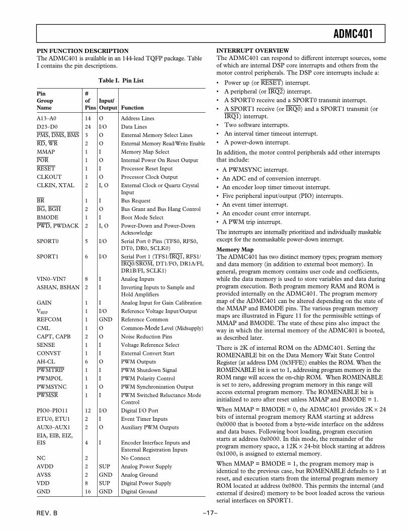
Memory MapThe ADMC401 has two distinct memory types; program memoryand data memory (in addition to external boot memory). Ingeneral, program memory contains user code and coefficients,while the data memory is used to store variables and data duringprogram execution. Both program memory RAM and ROM isprovided internally on the ADMC401. The program memorymap of the ADMC401 can be altered depending on the state ofthe MMAP and BMODE pins. The various program memorymaps are illustrated in Figure 11 for the permissible settings ofMMAP and BMODE. The state of these pins also impact theway in which the internal memory of the ADMC401 is booted,as described later.
There is 2K of internal ROM on the ADMC401. Setting theROMENABLE bit on the Data Memory Wait State ControlRegister (at address DM (0x3FFE)) enables the ROM. When theROMENABLE bit is set to 1, addressing program memory in theROM range will access the on-chip ROM. When ROMENABLEis set to zero, addressing program memory in this range willaccess external program memory. The ROMENABLE bit isinitialized to zero after reset unless MMAP and BMODE = 1.
When MMAP = BMODE = 0, the ADMC401 provides 2K × 24bits of internal program memory RAM starting at address0x0000 that is booted from a byte-wide interface on the addressand data buses. Following boot loading, program executionstarts at address 0x0000. In this mode, the remainder of theprogram memory space, a 12K × 24-bit block starting at address0x1000, is assigned to external memory.
When MMAP = BMODE = 1, the program memory map isidentical to the previous case, but ROMENABLE defaults to 1 atreset, and execution starts from the internal program memoryROM located at address 0x0800. This permits the internal (andexternal if desired) memory to be boot loaded across the variousserial interfaces on SPORT1.
REV. B
ADMC401
–18–
When MMAP = 1 and BMODE = 0, the internal programmemory RAM is mapped to the top of the program memory space(starting at address 0x3800) and no boot loading occurs. Programexecution starts from external program memory at address 0x0000.
Only with ROMENABLE = 1 are the internal ROM monitorand debugger features of the ADMC401 available for programdevelopment. Additionally, certain spaces of the memory maphave predefined functions as illustrated in Figure 12 where itcan be seen that address space 0x0000 to 0x005F is reserved forthe interrupt vector table.
VECTOR TABLE
USERPROGRAM
SPACE
0x000
ROMMONITOR
RESERVED
EXTERNALMEMORY
0x05F0x060
0x7FF0x800
0xFEF0xFF0
0xFFF0x1000
Figure 12. Detailed View of Program Memory Map withMMAP = BMODE = 1
The program memory interface can generate 0 to 7 wait statesfor external memory devices. The program memory wait statefield (PWAIT) in the System Control Register controls the numberof inserted wait states and defaults to 7. The structure of theSystem Control Register is shown at the end of the data sheet.
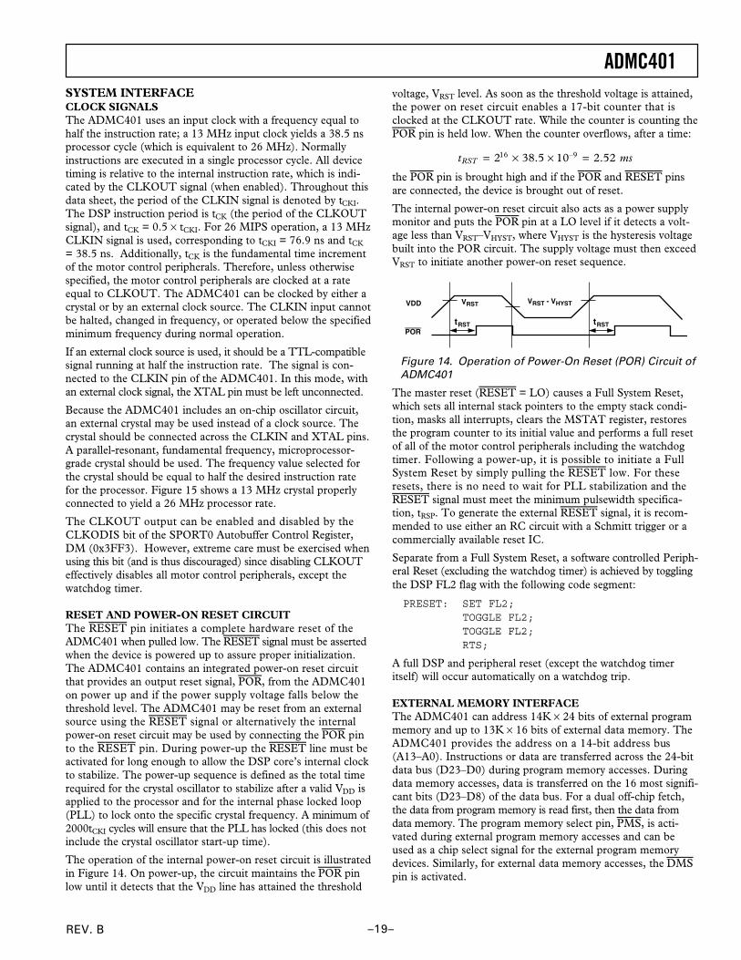
The data memory map of the ADMC401 is shown in Figure 13.The internal data memory RAM of the ADMC401 is arrangedas a single 1K × 16-bit block starting at address 0x3800. Inaddition, there are two 1K blocks of reserved data memoryspace; one block starting at address 0x2000 that is reserved forthe peripheral registers and one starting at address 0x3C00 thatis reserved for internal DSP core registers. Data memory waitstates are controlled by the DWAIT0, DWAIT1, DWAIT2,
DWAIT3 and DWAIT4 fields of the Data Memory Wait StateRegister (MEMWAIT) as illustrated in Figure 13. Followingreset, DWAIT0 = DWAIT1 = DWAIT2 = DWAIT 3 =DWAIT4 = 7. However, in standalone mode with MMAP =BMODE = 1, the internal monitor code writes 0 to these fivefields. For correct operation DWAIT2 must always be 0. Theconfiguration of the MEMWAIT register is shown at the end ofthe data sheet.
0x0000
8K EXTERNALMEMORY
0x23FF0x2400
0x1FFF0x2000 PERIPHERAL
REGISTERS
5K EXTERNALMEMORY
DSP COREREGISTERS/RESERVED
INTERNAL USERRAM
0x37FF0x3800
0x3BFF0x3C00
0x3FFF
0x3B5F0x3B60 RESERVED BY
MONITOR
0x0000
0x03FF0x0400
DWAIT0
0x2FFF0x3000
0x3FFF
DWAIT1
DWAIT2
NO WAITSTATES
0x07FF0x0800
DWAIT3
DWAIT40x3400
0x3800
Figure 13. Data Memory Map of the ADMC401
ROM CodeThe 2K × 24-bit block of internal program memory ROM start-ing at address 0x800 contains a monitor function that can beused to download and execute user programs via the serial port.In addition, the monitor function supports an interactive modein which commands are received and processed from a host thatis configured as a UART device. An example of such a host isthe Windows-based Motion Control Debugger that is part ofthe software development system for the ADMC401. In theinteractive mode, the host can access both the internal DSP andperipheral motor control registers of the ADMC401, read andwrite to both program and data memory, implement break-points and perform single-step operation as part of the programdebugging cycle. Again, this debugging feature is only availablewhen ROMENABLE = 1.
2K INTERNAL RAM(BOOTED FROM
BYTE-WIDE EPROM)
2K INTERNAL ROM(ROMENABLE = 1)
OR2K EXTERNAL
(ROMENABLE = 0)
12K EXTERNALMEMORY
0x0000
0x0FFF0x1000
0x07FF0x0800
0x3FFFMMAP = 0BMODE = 0
2K EXTERNALMEMORY
10K EXTERNALMEMORY
0x0000
0x0FFF0x1000
0x07FF0x0800
0x3FFFMMAP = 1BMODE = 0
2K INTERNAL RAM(BOOTED VIA
SPORT1)
2K INTERNAL ROM(ROMENABLE
DEFAULTS TO 1DURING RESET)
0x0000
0x0FFF0x1000
0x07FF0x0800
0x3FFFMMAP = 1BMODE = 1
0x3800
2K INTERNAL RAM
2K INTERNAL ROM(ROMENABLE = 1)
OR2K EXTERNAL
(ROMENABLE = 0)
12K EXTERNALMEMORY
Figure 11. Program Memory Map of ADMC401
ADMC401
–19–REV. B
SYSTEM INTERFACECLOCK SIGNALSThe ADMC401 uses an input clock with a frequency equal tohalf the instruction rate; a 13 MHz input clock yields a 38.5 nsprocessor cycle (which is equivalent to 26 MHz). Normallyinstructions are executed in a single processor cycle. All devicetiming is relative to the internal instruction rate, which is indi-cated by the CLKOUT signal (when enabled). Throughout thisdata sheet, the period of the CLKIN signal is denoted by tCKI.The DSP instruction period is tCK (the period of the CLKOUTsignal), and tCK = 0.5 × tCKI. For 26 MIPS operation, a 13 MHzCLKIN signal is used, corresponding to tCKI = 76.9 ns and tCK
= 38.5 ns. Additionally, tCK is the fundamental time incrementof the motor control peripherals. Therefore, unless otherwisespecified, the motor control peripherals are clocked at a rateequal to CLKOUT. The ADMC401 can be clocked by either acrystal or by an external clock source. The CLKIN input cannotbe halted, changed in frequency, or operated below the specifiedminimum frequency during normal operation.
If an external clock source is used, it should be a TTL-compatiblesignal running at half the instruction rate. The signal is con-nected to the CLKIN pin of the ADMC401. In this mode, withan external clock signal, the XTAL pin must be left unconnected.
Because the ADMC401 includes an on-chip oscillator circuit,an external crystal may be used instead of a clock source. Thecrystal should be connected across the CLKIN and XTAL pins.A parallel-resonant, fundamental frequency, microprocessor-grade crystal should be used. The frequency value selected forthe crystal should be equal to half the desired instruction ratefor the processor. Figure 15 shows a 13 MHz crystal properlyconnected to yield a 26 MHz processor rate.
The CLKOUT output can be enabled and disabled by theCLKODIS bit of the SPORT0 Autobuffer Control Register,DM (0x3FF3). However, extreme care must be exercised whenusing this bit (and is thus discouraged) since disabling CLKOUTeffectively disables all motor control peripherals, except thewatchdog timer.
RESET AND POWER-ON RESET CIRCUITThe RESET pin initiates a complete hardware reset of theADMC401 when pulled low. The RESET signal must be assertedwhen the device is powered up to assure proper initialization.The ADMC401 contains an integrated power-on reset circuitthat provides an output reset signal, POR, from the ADMC401on power up and if the power supply voltage falls below thethreshold level. The ADMC401 may be reset from an externalsource using the RESET signal or alternatively the internalpower-on reset circuit may be used by connecting the POR pinto the RESET pin. During power-up the RESET line must beactivated for long enough to allow the DSP core’s internal clockto stabilize. The power-up sequence is defined as the total timerequired for the crystal oscillator to stabilize after a valid VDD isapplied to the processor and for the internal phase locked loop(PLL) to lock onto the specific crystal frequency. A minimum of2000tCKI cycles will ensure that the PLL has locked (this does notinclude the crystal oscillator start-up time).
The operation of the internal power-on reset circuit is illustratedin Figure 14. On power-up, the circuit maintains the POR pinlow until it detects that the VDD line has attained the threshold
voltage, VRST level. As soon as the threshold voltage is attained,the power on reset circuit enables a 17-bit counter that isclocked at the CLKOUT rate. While the counter is counting thePOR pin is held low. When the counter overflows, after a time:
t msRST = × × =2 38 5 10 2 5216 9. .–
the POR pin is brought high and if the POR and RESET pinsare connected, the device is brought out of reset.
The internal power-on reset circuit also acts as a power supplymonitor and puts the POR pin at a LO level if it detects a volt-age less than VRST–VHYST, where VHYST is the hysteresis voltagebuilt into the POR circuit. The supply voltage must then exceedVRST to initiate another power-on reset sequence.
VDD
POR tRST tRST
VRST VRST - VHYST
Figure 14. Operation of Power-On Reset (POR) Circuit ofADMC401
The master reset (RESET = LO) causes a Full System Reset,which sets all internal stack pointers to the empty stack condi-tion, masks all interrupts, clears the MSTAT register, restoresthe program counter to its initial value and performs a full resetof all of the motor control peripherals including the watchdogtimer. Following a power-up, it is possible to initiate a FullSystem Reset by simply pulling the RESET low. For theseresets, there is no need to wait for PLL stabilization and theRESET signal must meet the minimum pulsewidth specifica-tion, tRSP. To generate the external RESET signal, it is recom-mended to use either an RC circuit with a Schmitt trigger or acommercially available reset IC.
Separate from a Full System Reset, a software controlled Periph-eral Reset (excluding the watchdog timer) is achieved by togglingthe DSP FL2 flag with the following code segment:
PRESET: SET FL2;TOGGLE FL2;TOGGLE FL2;RTS;
A full DSP and peripheral reset (except the watchdog timeritself) will occur automatically on a watchdog trip.
EXTERNAL MEMORY INTERFACEThe ADMC401 can address 14K × 24 bits of external programmemory and up to 13K × 16 bits of external data memory. TheADMC401 provides the address on a 14-bit address bus(A13–A0). Instructions or data are transferred across the 24-bitdata bus (D23–D0) during program memory accesses. Duringdata memory accesses, data is transferred on the 16 most signifi-cant bits (D23–D8) of the data bus. For a dual off-chip fetch,the data from program memory is read first, then the data fromdata memory. The program memory select pin, PMS, is acti-vated during external program memory accesses and can beused as a chip select signal for the external program memorydevices. Similarly, for external data memory accesses, the DMSpin is activated.
REV. B
ADMC401
–20–
Two control lines indicate the direction of the transfer. Memoryread, RD, is active low, signaling a read from external memoryand memory write; WR, is active low, signaling a write to exter-nal memory. Typically, the PMS line is connected to the CE(chip enable) of the external program memory and the RD lineis connected to the CE line of the external data memory. TheRD line is connected to the OE (output enable) and the WRline is connected to the WE (write enable) of both memories.
On-chip accesses (to internal program memory RAM and ROM)do not drive any of the external signals. The PMS, RD and theWR lines remain high (deasserted) and the address and databuses are three-stated during these internal accesses. Similarly,internal accesses to data memory (including internal DM RAMand peripheral and DSP core memory mapped registers) do notdrive external signals and the DMS, RD and the WR lines re-main high (deasserted) and the address and data buses are alsothree-stated.
External peripherals can also be connected externally and memorymapped to the external memory space of the ADMC401. The16 MSBs of the external data bus are connected internally to the16 bits of the internal data memory bus. Therefore, the datalines D23–D8 should be used for 16-bit peripherals.
BOOT LOADINGStandalone Mode (MMAP = BMODE = 1)Boot loading of the ADMC401 may occur in a number of differ-ent ways and is determined by the state of both the MMAP andBMODE pins. If both MMAP and BMODE are tied to VDD
(HI), the ADMC401 is placed in the so-called standalone modeand execution starts from internal program memory ROM ataddress 0x0800 following a power-on or reset. This starts execu-tion of the internal monitor function that first performs someinitialization functions (including writing 0 to the three datamemory wait state fields) and copies a default interrupt vectortable to addresses 0x0000–0x005F of program memory RAM.The monitor program next clears Bit 4 of the MODECTRLregister to connect the DR1A pin to the internal data receiveport (DR1) of SPORT1. In addition, Bit 5 of the MODECTRLregister is set. This connects the FL1 port of the DSP core tothe RFS1/SROM pin to act as a reset for a serial memory device.
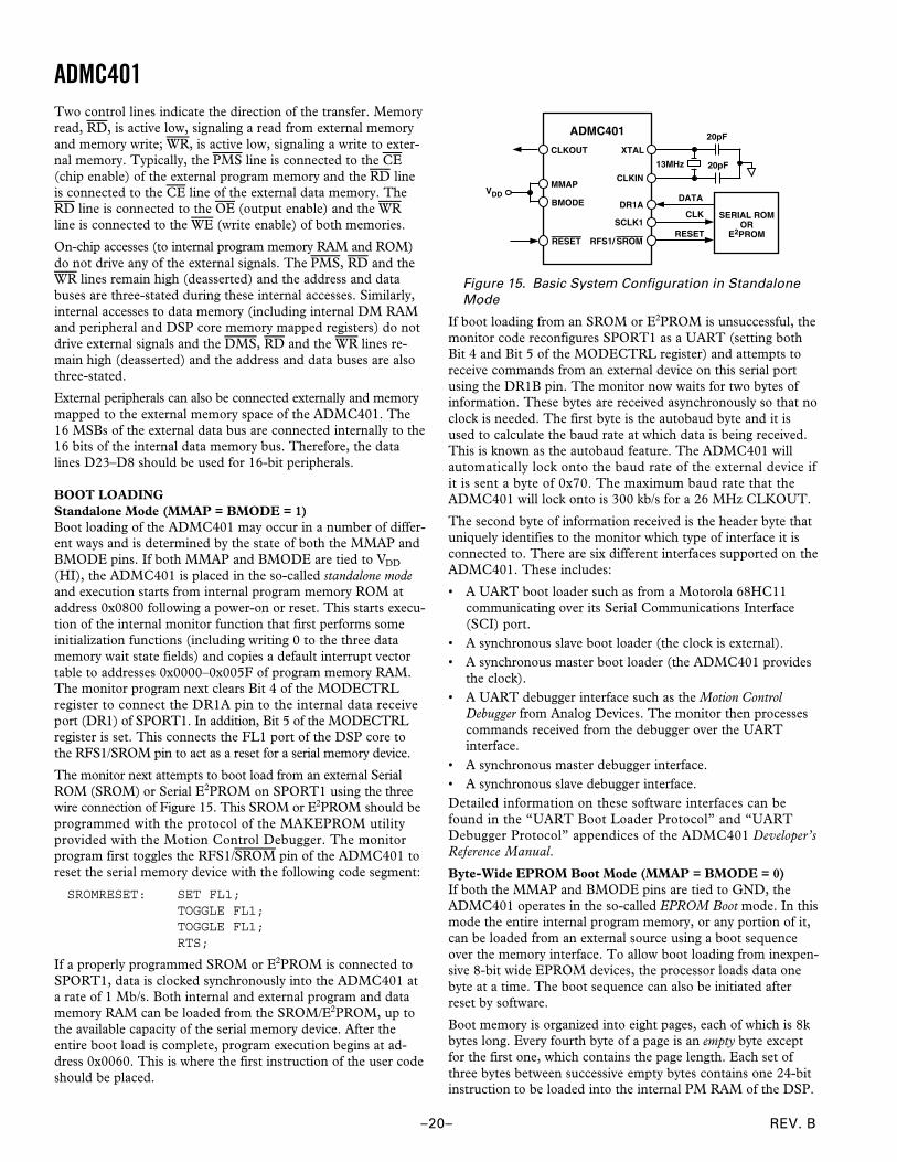
The monitor next attempts to boot load from an external SerialROM (SROM) or Serial E2PROM on SPORT1 using the threewire connection of Figure 15. This SROM or E2PROM should beprogrammed with the protocol of the MAKEPROM utilityprovided with the Motion Control Debugger. The monitorprogram first toggles the RFS1/SROM pin of the ADMC401 toreset the serial memory device with the following code segment:
SROMRESET: SET FL1;TOGGLE FL1;TOGGLE FL1;RTS;
If a properly programmed SROM or E2PROM is connected toSPORT1, data is clocked synchronously into the ADMC401 ata rate of 1 Mb/s. Both internal and external program and datamemory RAM can be loaded from the SROM/E2PROM, up tothe available capacity of the serial memory device. After theentire boot load is complete, program execution begins at ad-dress 0x0060. This is where the first instruction of the user codeshould be placed.
VDD
CLKOUT
MMAP
BMODE
RESET
XTAL
CLKIN
DR1A
SCLK1
RFS1/ SROM
SERIAL ROMOR
E2PROM
ADMC401
13MHz
20pF
20pF
DATA
CLK
RESET
Figure 15. Basic System Configuration in StandaloneMode
If boot loading from an SROM or E2PROM is unsuccessful, themonitor code reconfigures SPORT1 as a UART (setting bothBit 4 and Bit 5 of the MODECTRL register) and attempts toreceive commands from an external device on this serial portusing the DR1B pin. The monitor now waits for two bytes ofinformation. These bytes are received asynchronously so that noclock is needed. The first byte is the autobaud byte and it isused to calculate the baud rate at which data is being received.This is known as the autobaud feature. The ADMC401 willautomatically lock onto the baud rate of the external device ifit is sent a byte of 0x70. The maximum baud rate that theADMC401 will lock onto is 300 kb/s for a 26 MHz CLKOUT.
The second byte of information received is the header byte thatuniquely identifies to the monitor which type of interface it isconnected to. There are six different interfaces supported on theADMC401. These includes:
• A UART boot loader such as from a Motorola 68HC11communicating over its Serial Communications Interface(SCI) port.
• A synchronous slave boot loader (the clock is external).• A synchronous master boot loader (the ADMC401 provides
the clock).• A UART debugger interface such as the Motion Control
Debugger from Analog Devices. The monitor then processescommands received from the debugger over the UARTinterface.
• A synchronous master debugger interface.• A synchronous slave debugger interface.Detailed information on these software interfaces can befound in the “UART Boot Loader Protocol” and “UARTDebugger Protocol” appendices of the ADMC401 Developer’sReference Manual.
Byte-Wide EPROM Boot Mode (MMAP = BMODE = 0)If both the MMAP and BMODE pins are tied to GND, theADMC401 operates in the so-called EPROM Boot mode. In thismode the entire internal program memory, or any portion of it,can be loaded from an external source using a boot sequenceover the memory interface. To allow boot loading from inexpen-sive 8-bit wide EPROM devices, the processor loads data onebyte at a time. The boot sequence can also be initiated afterreset by software.
Boot memory is organized into eight pages, each of which is 8kbytes long. Every fourth byte of a page is an empty byte exceptfor the first one, which contains the page length. Each set ofthree bytes between successive empty bytes contains one 24-bitinstruction to be loaded into the internal PM RAM of the DSP.
ADMC401
–21–REV. B
The page length is read first and then bytes are loaded from thetop of the page downwards. This causes shorter booting timesfor shorter pages. The length of the boot page is given as:
page length = (number of 24-bit PM words/8) – 1
That is, a page length of 0 causes the boot address generator togenerate byte addresses for eight words that reside in 32 sequen-tial EPROM locations.
A PROM splitter utility (SPL21), part of the Motion ControlDebugger tool set, calculates the proper page length for yourprogram and orders the bytes of your program according to theproper protocol. More detailed information about the use ofthis PROM splitter utility can be found in the “Booting fromExternal EPROM with MMAP = BMODE = 0” chapter of theADMC401’s Developer’s Reference Manual.
Following a reset, if both MMAP and BMODE are LO, theboot sequence always boot loads page 0. After reset, boot load-ing can occur under program control from any one of up toeight different boot pages. The boot page select field (BPAGE)in the memory mapped System Control Register specifies whichboot page is to be loaded. To boot from a specific boot page,first set the BPAGE bits to the desired value and set the bootforce bit (BFORCE) of the System Control Register to initiate aboot sequence.
The ADMC401 can boot its internal program memory from asingle byte-wide CMOS EPROM such as the 27C64 or the27C512. A low cost commodity-grade EPROM with an indus-try-standard access time can be used. The number of wait statesfor the boot memory access is selected in the BWAIT field ofthe System Control Register. This field can be set to any valuefrom 0 to 7 to set the number of wait states. The default valuefor the BWAIT field is 7 so that seven wait states are insertedinto the reset-initiated boot loading sequence.
Timing of the boot memory access is identical to that of externalprogram memory or external data memory accesses, except thatthe active strobe is BMS rather than PMS or DMS. To addresseight pages of 8K bytes each, 16 address lines are needed. Theleast significant 14 bits are output on the 14-bit address bus(A13 to A0) while the most significant two bits are output onthe 2 MSBs of the data bus (D23 and D22) during boot memoryaccesses. The data is read from the middle eight bits of the databus (D15 to D8).
The development tools for the ADMC401 support the creationof EPROM target files capable of boot loading both internal andexternal program and data memory.
External Memory Mode (BMODE = 0, MMAP = 1)In this mode, with BMODE tied to GND and MMAP tied toVDD, the ADMC401 is placed in external memory mode andthere is no boot loading. The effect of this mode is that theinternal 2K bank of program memory RAM is relocated fromthe bottom of memory (starting at address 0x0000) to the top ofthe program memory space (at address 0x3800). In this mode,program execution starts at external memory address 0x0000, atwhich point the first instruction must be placed.
The mode in which BMODE = 1 and MMAP = 0 is not allowedon the ADMC401 and is an illegal state. The operation of theADMC401 is neither guaranteed nor defined with BMODE = 1and MMAP = 0.
BUS REQUEST/GRANTThe ADMC401 can relinquish control of the external data andaddress buses to an external device. The external device requeststhe bus by asserting (low) the bus request signal BR. BR is anasynchronous input and if the ADMC401 is not performing anexternal access, it responds to the active BR input in the follow-ing processor cycle by:• Three-stating the data and address buses and the PMS,
DMS, BMS, RD and WR output drivers.• Asserting the bus grant (BG) signal, and• Halting program execution (unless Go Mode is enabled).
If Go Mode is enabled, (using the ENA G-MODE instruction)the ADMC401 continues to execute instructions from its inter-nal memory. It will not halt program execution until it encoun-ters an instruction that requires an external access, which includesan access to any motor control peripheral register. If Go Modeis not enabled, the ADMC401 always halts before granting thebus. The processor’s internal state is not affected by grantingthe bus, and the serial ports remain active during a bus grant,whether or not the processor core halts.
If the ADMC401 is performing an external access when the BRsignal is asserted, it will not grant the buses until the cycle afterthe access completes. The entire instruction does not need to becompleted when the bus is granted. If a single instruction re-quires two external accesses, the bus will be granted between thetwo accesses. The second access is performed after BR is re-moved. When the BR input is released, the ADMC401 releasesthe BG signal, re-enables the output drivers and continues pro-gram execution from the point where it stopped. BG is alwaysdeasserted in the same cycle that the removal of BR is recognized.
The bus request feature operates at all times, including whenthe ADMC401 is booting and when RESET is active. DuringRESET, BG is asserted in the same cycle that BR is recognized.During booting, the bus is granted after the completion of load-ing of the current byte (including any wait states). Using the busrequest during booting is one way to bring the booting operationunder control of a host computer.
The ADMC401 has an additional output, Bus Grant Hang,BGH, which lets it operate in a multiprocessor system with aminimum number of wasted cycles. The BGH pin asserts whenthe ADMC401 is ready to execute an instruction but is stoppedbecause the external bus is granted to another device. The otherdevice can release the bus by deasserting bus request. Once thebus is released, the ADMC401 deasserts BG and BGH andexecutes the external access.
POWER-DOWN MODESThe ADMC401 includes a power-down feature that allows thedevice to enter a very low power dormant state through hard-ware or software control. In the power-down mode:
• Internal clocks are disabled• Processor registers and memory contents are maintained• Ability to recover from power-down in less than 100tCKI
cycles• Interrupt support for housekeeping code before entering
power-down and after recovering from power-down• User-selectable power-up context
REV. B
ADMC401
–22–
Entering Power-DownThe power-down sequence is initiated by applying a high-to-lowtransition on the PWD pin or by setting the power-down forcecontrol bit (PDFORCE) of the SPORT1 autobuffer/power-down control register. The DSP core then vectors to the non-maskable power-down interrupt vector at address 0x002C. Caremust be taken to ensure that multiple power-down interrupts donot occur or else stack overflow may result. The interrupt ser-vice routine at address 0x002C can be used to execute any num-ber of housekeeping instructions prior to the processor enteringthe power-down mode. Typically, this is used to configure thepower-down state, disable on-chip peripherals and clear pendinginterrupts. The DSP subsequently enters the power-down modewhen it executes the IDLE instruction (while PWD is asserted).The processor may take either one or two cycles to power down,depending on internal clock states during execution of the IDLEinstruction. All register and memory contents are maintained inpower-down. Also, all active outputs are held in whatever statethey are in before going into power-down. If an RTI instructionis executed before the IDLE instruction, the processor returnsfrom the power-down interrupt and the power-down sequence isaborted.
Exiting Power-DownThe power-down mode can be exited with the use of the PWDpin or with the RESET pin. There are also several user-select-able modes for startup from power-down which specify a start-up delay as well as specify the program flow after startup. Thisallows the program to resume from where it left off beforepower-down, or for the program context to be cleared. Applyinga low-to-high transition on the PWD pin will take the processorout of power-down. The amount of time it takes for the proces-sor to come out of power-down is controllable with the delaystartup from power-down control bit (XTALDELAY, Bit 14 ofthe Power-Down Control Register or SPORT1 AutobufferControl Register). If this bit is cleared, no additional delay overthe quick startup (100 cycles) is introduced. If this bit is set, adelay of 4096 cycles is introduced.
The context for exiting power-down is set by Bit 12 (PUCR) ofthe Power-Down Control Register. If this bit is cleared, afterexiting power-down the processor will continue to execute in-structions following the IDLE instruction after the low-to-hightransition on the PWD pin. When the RTI instruction is en-countered in the interrupt service routine for the power-down,operation is returned to the main routine. If the PUCR bit isset, for a “clear context”, the processor resumes operation frompower-down by clearing the PC, STATUS, LOOP and CNTRregisters. The IMASK and ASTAT registers are cleared and theSSTAT goes to 0x55. The processor starts execution at address0x0000.
Active output pins retain their states during power-down. Inaddition, interrupts are latched and can be serviced if theADMC401 exits power-down with PUCR = 0. It is possible toclock data into or out of the serial ports during power-downby supplying an external serial clock. Data clocked into theADMC401 will remain in the RX registers. These activitiescause additional power consumption.
If RESET is activated while the ADMC401 is in the power-down mode, power down is exited, and a normal Full SystemReset Sequence is initiated, (which depends upon the settings ofMMAP and BMODE for the boot method as usual). When
exiting power-down with RESET, the XTALDELAY control bitis ignored.
Startup Time After Power-DownThe time required to exit the power-down state depends on themethod used to exit power-down. Unlike the standard ADSP-21xx products, the XTALDIS bit of the Power-Down Registerhas no effect on the ADMC401 so that it is not possible to avoidthe power drain caused by the XTAL pin toggling. When theprocessor comes out of power-down by either the PWD or RESETpins, it will begin executing after a maximum startup time of100 CLKIN cycles as long as the clock oscillator is stable and atthe same frequency as before power-down.
If the external clock is unstable when the ADMC401 exitspower-down, the XTALDELAY control bit can be used toinsert an additional 4096 cycle delay into the startup time. Thisdelay can only be inserted when the ADMC401 is brought outof power-down by the PWD pin.
If the processor is taken out of power-down by the RESET line,and the clock is stable and at the same frequency as beforepower-down, the RESET need only be held for five cycles.
The PWDACK PinThe PWDACK pin is an output that indicates when the ADMC401is in the power-down mode. This pin is driven high by the pro-cessor when it has powered down. It is driven low after theprocessor has completed the power-up sequence. A low level onthe PWDACK pin also indicates that there is a valid CLKOUTsignal and that instruction execution has begun.
When power-down is terminated with the RESET pin or a start-up delay is selected, a low level on the PWDACK pin only indi-cates the start of oscillations on the CLKOUT pin. It will notnecessarily indicate the start of instruction execution.
The state of PWDACK and also the CLKOUT signal is unde-fined during the first 100 cycles of the initial reset.
Using Power-Down as a Nonmaskable InterruptThe power-down interrupt is never masked. It is possible to usethis interrupt for other purposes, if desired. The ADMC401 doesnot go into power-down until the IDLE instruction is executed.If an RTI is executed instead, before an IDLE instruction, theprocessor returns from the power-down interrupt service outlineand the power-down sequence is aborted.
THE ANALOG-TO-DIGITAL CONVERSIONSYSTEMOVERVIEW OF ADC SYSTEMThe ADMC401 contains a fast, high accuracy, multiple-inputanalog-to-digital conversion system with simultaneous samplingcapabilities. This A/D conversion system permits the fast, accu-rate conversion of currents, voltages and other signals needed inhigh performance motor control systems. A functional blockdiagram of the entire ADC system is shown in Figure 16.
The ADC system permits up to eight dedicated analog inputs allto be converted in under 2 µs (at 26 MHz) through a single 12-bit pipeline flash ADC. The entire ADC system (includingmultiplexing and the sample and hold amplifiers) operates at aclock rate equal to a quarter of the DSP instruction rate. Analoginput voltages of up to 4.0 V p-p can be converted. The inputsignals are divided into two banks of four signals each, withVIN0 to VIN3 making up one bank and VIN4 to VIN7 makingup the second bank. There are also two dedicated inputs (ASHAN
ADMC401
–23–REV. B
and BSHAN) to the inverting terminal of the two sample andhold amplifiers (SHA) so that external signals can be correctlybiased about the nominal operating range of the ADC.
ADC0(15...0)
ADC1(15...0)
ADC2(15...0)
ADC3(15...0)
ADC4(15...0)
ADC5(15...0)
ADC6(15...0)
ADC7(15...0)
ADCOTR(7...0)
ADCSTAT(4...0)
ADCCTRL(4...0)
MULTIPLEXER, SHA AND ADC CONTROL
INTERNALREFERENCESIGNALS
ASHAN
VIN0
VIN1VIN2
VIN3
VIN4
VIN5
VIN7
BSHAN
PWMSYNC
CONVST
CLKOUT
CAPTCAPB
VREF
REFCOMSENSE
CML
VIN6
VOLTAGEREFERENCEGENERATION& CONTROL
12-BITPIPELINE
FLASH ADC
DATA
CONTROL SIGNALS
END OFCONVERSION
OUTOF
RANGE
MUX
MUX
MUX
SHA A
ADCXTRA(15...0)
GAIN
SHA B
PWMSYNC (FROM PWM PERIPHERAL)
Figure 16. Functional Block Diagram of the ADC Systemof the ADMC401
The basic architecture of the ADC system consists of a four-stage pipeline architecture (the A/D core) with wideband inputsample and hold amplifiers. Excluding the last stage, each stageof the pipeline consists of a low resolution flash A/D connectedto a switched capacitor DAC and interstage residue amplifier(MDAC). The reside amplifier amplifies the difference betweenthe reconstructed DAC output and the flash input for the nextstage in the pipeline. The last stage of the pipeline simply con-sists of a flash A/D. The pipeline architecture allows a greaterthroughput rate at the expense of pipeline delay or latency. Thismeans that while the converter is capable of capturing a newinput sample every ADC clock cycle, it actually takes 3 1/2 ADCclock cycles for the conversion process of any input to be fullyprocessed and appear at the output.
The ADC may operate in two basic conversion modes, Simulta-neous Sampling or Sequential Sampling. The operating mode isselected by dedicated bits in the ADCCTRL register. In theSimultaneous Sampling mode, two analog inputs (one from eachbank) are sampled simultaneously so that VIN0 and VIN4,VIN1 and VIN5, VIN2 and VIN6, VIN3 and VIN7 representfour pairs of simultaneously sampled inputs. In the alternativesequential operating mode, there is no simultaneous sampling,and the analog inputs are sampled and converted one after theother (i.e., VIN0 followed by VIN1 followed by VIN2, etc.). Inthis mode, successive analog inputs are sampled an ADC clockperiod (or four DSP clock cycles) apart.
The conversion sequence may be initiated either internally (syn-chronized to the PWM generation) or from an external event onthe CONVST pin. In the default Simultaneous Sampling mode ofoperation, the internal control logic simultaneously samples thefirst pair of input signals (VIN0 and VIN4) following the con-vert start command. Subsequently, these inputs are multiplexedinto the 12-bit analog-to-digital converter. After a delay of twoADC clock cycles, the second pair of analog inputs (VIN1 andVIN5) are sampled simultaneously and then multiplexed intothe ADC. This process continues until all four pairs of analoginputs have been sampled and converted. As the conversion fora given analog input channel is completed, the correspondingdigital number is written to a dedicated 16-bit, twos comple-ment, left-aligned register that is memory mapped to the datamemory space of the DSP core. The ADC data register ADC0stores the conversion result for the signal on VIN0, etc.
Following the end of conversion of each pair of analog inputs, adedicated bit is set in the ADCSTAT register. The result of thishighly efficient pipelined structure is that all eight ADC dataregisters will contain valid conversion results less than 2 µs (at26 MHz) after the convert start command. At this point a dedi-cated ADC interrupt will be generated. Alternatively, if data isrequired sooner, the ADCSTAT register can be polled to detectwhen a given pair of analog inputs have been successfully con-verted, except in Sequential Sampling mode.
Once the conversion sequence has been completed and all eightADC data registers have been updated, the entire ADC structureautomatically reverts to the Single Channel mode and continu-ously converts the analog input on the VIN0 pin. The results ofthis conversion are placed in the additional ADCXTRA registerand are updated once every ADC clock cycle. This feature couldbe used to continuously monitor a single analog input on theVIN0 pin.
There are two additional modes of operation of the ADC systemthat may be used for offset and gain calibration of the entiresystem. In the Offset Calibration mode, all analog inputs (VIN0to VIN7, GAIN, ASHAN and BSHAN) are disconnected fromthe inputs to the sample and hold amplifiers. Instead, bothterminals of each sample and hold amplifiers are connectedtogether and to the voltage reference. Following a conversionsequence, the data in the ADC data register can be taken as ameasure of any offset in the sample and hold amplifiers andADC. Additionally, in the Gain Calibration mode, the dedicatedanalog input GAIN is applied to the noninverting terminal ofboth sample and hold amplifiers. Any number of precise exter-nal voltages can be applied to this pin to measure and correctfor any gain errors, if required.
Along with each data output from the A/D converter, an Out-of-Range (OTR) bit is set if the signal exceeds the permissibleinput voltage span. In normal conversion, the eight OTR bits forthe eight analog inputs are stored in the ADCOTR register, withone bit for each analog input. The OTR bit for the ADCXTRAregister is stored in the ADCSTAT register.
The ADC may use either an internally generated 2.0 V precisionreference voltage or an externally supplied reference voltagelevel at the VREF pin. The operating mode is selected by theconnection of the SENSE pin.
REV. B
ADMC401
–24–
CONVERT START COMMANDThe analog-to-digital conversion process of the ADMC401 maybe started by either an internal or an external command. Bit 0 ofthe ADCCTRL register determines whether internal or externalconvert start mode is enabled. If Bit 0 of the ADCCTRL regis-ter is cleared, internal convert start mode is selected, and theADC conversion process is started on the rising edge of thePWMSYNC signal. This results in one conversion sequence perPWM switching period (at the start of each period) when thePWM generation unit operates in the single update mode. In thedouble update operating mode, there are two conversion se-quences per PWM switching period (one at the start and one inthe middle of each period). In internal convert start mode, inorder to ensure correct synchronization and jitter-free operation,it is essential that the value written to the PWMTM register be amultiple of four. In other words, the two LSBs of the valuewritten to the PWMTM register must both be 0.
If Bit 0 of the ADCCTRL register is set, external convert startmode is selected. In this mode, the conversion process is startedon the occurrence of a rising edge on the CONVST pin. Addi-tionally, the start of conversion can be placed under softwarecontrol by externally connecting one of the programmable input/output (PIO) lines to the CONVST pin and generating a risingedge by writing to the appropriate bit of the PIODATA register.
By default, following reset, Bit 0 of the ADCCTRL register iscleared so that internal convert start mode is selected.
ADC CLOCK SIGNALSThe ADC consists of a pipeline flash architecture and is clockedat a quarter of the DSP instruction rate. All of the timing of theADC system (including control of the multiplexers and sampleand hold amplifiers) is regulated by this clock signal and it de-termines the total conversion time for all of the channels as wellas the delay between sampling of successive pairs of analoginputs. The ADC clock rate is internally fixed and may not bechanged. The period of the ADC clock, tCKADC is related to theDSP CLKOUT period by:
t tCKADC CK= ×4
A DSP rate of 26 MHz corresponds to a tCKADC of approxi-mately 154 ns.
ANALOG INPUT CONFIGURATION AND OVERVIEWFigure 17 is a simplified model of the ADC input structure forone channel (VIN0) of the ADC system of the ADMC401. Thismodel applies to all eight input channels. The internal multi-plexers are used to switch the various analog inputs to the A/Dconverter. For analog inputs VIN0 to VIN3, there is a singlecommon terminal (ASHAN) that is the inverting input to theinternal differential sample and hold amplifier. For the inputsignals, VIN4 to VIN7, the equivalent input is BSHAN. Thevalue VREF (internally generated voltage reference or externallyapplied voltage reference on the VREF pin) defines the maximuminput voltage to the A/D core. The minimum input voltage tothe A/D core is automatically defined as –VREF.
+VREF
–VREF
12VIN0
ASHAN
VCOREA/D
CORE
Figure 17. Equivalent Functional Input Circuit of ADCSystem
The dc voltage on the VREF pin sets the common-mode voltageof the A/D converter of the ADMC401. For example, whenusing the internal 2.0 V reference, the input level will also becentered about 2.0 V. The ADC inputs of the ADMC401 canbe configured for single ended operation, where the invertingterminals (ASHAN and BSHAN) are connected directly to thereference voltage level, and the analog inputs (VIN0 to VIN7)are driven by analog signals with a 4.0 V p-p range. The VIN0to VIN7 inputs are unipolar so that when operating from theinternal 2.0 V reference, these signals can range from 0 V to4 V. The recommended single-ended input configuration for asingle analog input channel of the ADMC401 is shown in Fig-ure 18. The input to the A/D converter must be driven by anoperational amplifier with sufficient drive strength so that theA/D performance is not degraded. Sufficient drive strength isthe ability to drive a load of 6 pF static and 4 pF switched fromground (capacitive) to settle within ±1.0 mV within 70 ns. InFigure 18, the operational amplifier is shown configured as asimple noninverting input buffer. Of course, the operationalamplifier stage could also be used to implement any necessarylevel shifting and/or filtering of the input signal.
+V
–V
VIN0
ASHAN
VREF
SENSE
ADMC401
RS
RS
10F 0.1F
4V
0V
Figure 18. Typical Single-Ended Input Configuration forADMC401
From Figure 17, it is clear that the input to the A/D core issimply given by:
V VIN ASHANCORE = 0–
which must satisfy the condition:
–V V VREF CORE REF≤ ≤
where VREF is the voltage at the VREF pin of the ADMC401(either internally generated or externally supplied). There is anadditional limit placed on the valid operating range for the VIN0and ASHAN inputs that is bounded by the power supply of theADMC401:
AV V VIN AV V
AV V ASHAN AV V
SS DD
SS DD
– . .
– . .
0 3 0 0 3
0 3 0 3
≤ ≤ +
≤ ≤ +
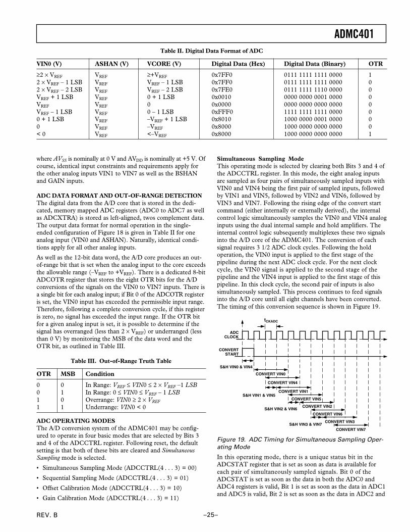
ADMC401
–25–REV. B
Simultaneous Sampling ModeThis operating mode is selected by clearing both Bits 3 and 4 ofthe ADCCTRL register. In this mode, the eight analog inputsare sampled as four pairs of simultaneously sampled inputs withVIN0 and VIN4 being the first pair of sampled inputs, followedby VIN1 and VIN5, followed by VIN2 and VIN6, followed byVIN3 and VIN7. Following the rising edge of the convert startcommand (either internally or externally derived), the internalcontrol logic simultaneously samples the VIN0 and VIN4 analoginputs using the dual internal sample and hold amplifiers. Theinternal control logic subsequently multiplexes these two signalsinto the A/D core of the ADMC401. The conversion of eachsignal requires 3 1/2 ADC clock cycles. Following the holdoperation, the VIN0 input is applied to the first stage of thepipeline during the next ADC clock cycle. For the next clockcycle, the VIN0 signal is applied to the second stage of thepipeline and the VIN4 input is applied to the first stage of thispipeline. In this clock cycle, the second pair of inputs is alsosimultaneously sampled. This process continues to feed signalsinto the A/D core until all eight channels have been converted.The timing of this conversion sequence is shown in Figure 19.
CONVERT VIN7S&H VIN3 & VIN7
S&H VIN1 & VIN5
S&H VIN2 & VIN6
CONVERTSTART
ADCCLOCK
S&H VIN0 & VIN4
CONVERT VIN0
CONVERT VIN4
CONVERT VIN1
CONVERT VIN5
CONVERT VIN2
CONVERT VIN6
CONVERT VIN3
tCKADC
Figure 19. ADC Timing for Simultaneous Sampling Oper-ating Mode
In this operating mode, there is a unique status bit in theADCSTAT register that is set as soon as data is available foreach pair of simultaneously sampled signals. Bit 0 of theADCSTAT is set as soon as the data in both the ADC0 andADC4 registers is valid, Bit 1 is set as soon as the data in ADC1and ADC5 is valid, Bit 2 is set as soon as the data in ADC2 and
Table II. Digital Data Format of ADC
VIN0 (V) ASHAN (V) VCORE (V) Digital Data (Hex) Digital Data (Binary) OTR
≥2 × VREF VREF ≥+VREF 0x7FF0 0111 1111 1111 0000 12 × VREF – 1 LSB VREF VREF – 1 LSB 0x7FF0 0111 1111 1111 0000 02 × VREF – 2 LSB VREF VREF – 2 LSB 0x7FE0 0111 1111 1110 0000 0VREF + 1 LSB VREF 0 + 1 LSB 0x0010 0000 0000 0001 0000 0VREF VREF 0 0x0000 0000 0000 0000 0000 0VREF – 1 LSB VREF 0 – 1 LSB 0xFFF0 1111 1111 1111 0000 00 + 1 LSB VREF –VREF + 1 LSB 0x8010 1000 0000 0001 0000 00 VREF –VREF 0x8000 1000 0000 0000 0000 0< 0 VREF <–VREF 0x8000 1000 0000 0000 0000 1
where AVSS is nominally at 0 V and AVDD is nominally at +5 V. Ofcourse, identical input constraints and requirements apply forthe other analog inputs VIN1 to VIN7 as well as the BSHANand GAIN inputs.
ADC DATA FORMAT AND OUT-OF-RANGE DETECTIONThe digital data from the A/D core that is stored in the dedi-cated, memory mapped ADC registers (ADC0 to ADC7 as wellas ADCXTRA) is stored as left-aligned, twos complement data.The output data format for normal operation in the single-ended configuration of Figure 18 is given in Table II for oneanalog input (VIN0 and ASHAN). Naturally, identical condi-tions apply for all other analog inputs.
As well as the 12-bit data word, the A/D core produces an out-of-range bit that is set when the analog input to the core exceedsthe allowable range (–VREF to +VREF). There is a dedicated 8-bitADCOTR register that stores the eight OTR bits for the A/Dconversions of the signals on the VIN0 to VIN7 inputs. There isa single bit for each analog input; if Bit 0 of the ADCOTR registeris set, the VIN0 input has exceeded the permissible input range.Therefore, following a complete conversion cycle, if this registeris zero, no signal has exceeded the input range. If the OTR bitfor a given analog input is set, it is possible to determine if thesignal has overranged (less than 2 × VREF) or underranged (lessthan 0 V) by monitoring the MSB of the data word and theOTR bit, as outlined in Table III.
Table III. Out-of-Range Truth Table
OTR MSB Condition
0 0 In Range: VREF ≤ VIN0 ≤ 2 × VREF –1 LSB0 1 In Range: 0 ≤ VIN0 ≤ VREF – 1 LSB1 0 Overrange: VIN0 ≥ 2 × VREF1 1 Underrange: VIN0 < 0
ADC OPERATING MODESThe A/D conversion system of the ADMC401 may be config-ured to operate in four basic modes that are selected by Bits 3and 4 of the ADCCTRL register. Following reset, the defaultsetting is that both of these bits are cleared and SimultaneousSampling mode is selected.
• Simultaneous Sampling Mode (ADCCTRL(4 . . . 3) = 00)
• Sequential Sampling Mode (ADCCTRL(4 . . . 3) = 01)
• Offset Calibration Mode (ADCCTRL(4 . . . 3) = 10)
• Gain Calibration Mode (ADCCTRL(4 . . . 3) = 11)
REV. B
ADMC401
–26–
ADC6 is valid and Bit 3 is set when the data in ADC3 andADC7 is valid. At the start of the next conversion sequence, allbits of the ADCSTAT register are cleared. Additionally, at theend of the complete conversion sequence (when the data in theADC7 register is valid), a dedicated ADC interrupt is generated.This interrupt can be masked and controlled by the PIC block.
Depending on initial synchronization delays, the worst case totalconversion time (defined as the duration from the rising edge ofthe convert start command to the generation of the ADC inter-rupt) for all eight channels is:
tCONV = 49 × tCK
which corresponds to 1.88 µs for a DSP instruction rate of26 MHz. Additionally, in this operating mode, the time delaybetween sampling of successive pairs of analog inputs is 8tCK or308 ns (at 26 MHz).
Sequential Sampling ModeThis operating mode is selected by setting Bit 3 and clearingBit 4 of the ADCCTRL register. In this operating mode, simul-taneous sampling is abandoned and the A/D conversion se-quence samples each analog input sequentially. Therefore, inthe first ADC clock period, VIN0 is sampled and held by thefirst sample and hold amplifier. In the second clock period, theheld sample of VIN0 is applied to the first stage of the ADCpipeline and the VIN1 signal is sampled. This process continuesuntil each of the analog inputs has been sequentially sampledand converted (i.e., VIN0 followed by VIN1 followed by VIN2,etc.). In this operating mode, the total conversion time is thesame as the Simultaneous Sampling mode. However, successivechannels are sampled at 4tCK (or 154 ns at 26 MHz) intervals.In this mode, Bits 0 to 3 of the ADCSTAT register are all settogether when all eight conversions are complete. The interruptis generated, as before, when the data in the ADC7 register is valid.
Offset Calibration ModeIn order to maintain the high accuracy of the ADC system ofthe ADMC401, it may be necessary to measure and compensatefor any intrinsic offset and/or gain errors in the A/D conversionsystem. The Offset Calibration mode, which is selected by settingBit 4 and clearing Bit 3 of the ADCCTRL register, is intendedto be used for measuring any offsets in the sample and holdamplifiers. When this mode is selected, all analog inputs (VIN0to VIN7, ASHAN and BSHAN) are disconnected from theinputs to the sample and hold amplifiers, and the SHA inputsare internally connected together and to the reference voltage(at the VREF pin). Since these connections are in effect onlyduring the conversion sequence, a complete conversion se-quence must be initiated. Following the end of conversion,the data in the ADC0 to ADC3 registers may be taken as fourseparate measurements of the offset of the first sample and holdamplifier. Similarly, the data in the ADC4 to ADC7 registersmay be taken as measurements of the offset associated with thesecond sample and hold amplifier. These data values could beaveraged to obtain an offset value for each sample and holdamplifier that could be stored and used to compensate all futuremeasurements. The end of conversion status bits are updatedand the interrupt is generated in a manner identical to the Si-multaneous Sampling mode.
Gain Calibration ModeIt may be desirable to measure and compensate for any gainerrors associated with the A/D conversion process across the
entire input voltage span of the A/D system. The Gain Calibra-tion mode, selected by setting both Bits 3 and 4 of the ADCCTRLregister, is designed to offer significant user flexibility in deter-mining the amount of gain compensation that may be required.In this mode the dedicated GAIN input pin is internally con-nected directly to the noninverting input of each sample andhold amplifier. The user may apply different precise analogvoltages across the input voltage span to this pin to measuregain errors over the operating range.
A complete conversion sequence for each different GAIN inputmust be initiated. Following the end of conversion, the data inthe ADC0 to ADC3 registers may be used to calculate fourseparate measurements of the gain error of the first sample andhold amplifier. Similarly, the data in the ADC4 to ADC7 regis-ters may be used to calculate the gain associated with the secondsample and hold amplifier. These data values could be averagedto obtain gain error values for each sample and hold amplifierthat could be stored and used to compensate all future measure-ments. The end of conversion status bits are updated and theinterrupt is generated in a manner identical to the Simulta-neous Sampling mode.
ADCXTRA REGISTERFollowing the end of conversion sequence in any of the fouroperating modes, the A/D system reverts to its Single Channelmode. In this configuration, the multiplexers are set such thatthe VIN0 input is continuously sampled and converted. The resultsof these conversions are placed in the dedicated ADCXTRAregister that is updated with the results of a new conversionevery ADC clock period (or 154 ns at 26 MHz). This featurepermits the continuous tracking of a single analog input, if re-quired. The OTR bit for these conversions is placed in Bit 4 ofthe ADCSTAT register. No interrupt is generated followingthese conversions and no other status bits are generated. TheADCXTRA register is not updated during the conversion se-quence of any of the four operating modes.
VOLTAGE REFERENCE OPERATIONThe ADMC401 contains an onboard bandgap reference thatcan be used to provide a precise 2.0 V output for use by the A/Dsystem and externally on the VREF pin for biasing and level–shifting functions. Additionally, the ADMC401 may be config-ured to operate with an external reference applied to the VREF
pin. The SENSE pin is used to select between internal andexternal references.
The actual reference voltages used by the internal ADC circuitryof the ADMC401 appear on the CAPT and CAPB pins. Forcorrect operation of the internal voltage reference generationcircuitry, either with internal or external reference, it is neces-sary to add a capacitor network between these pins, as shown inFigure 20. A 10 µF tantalum capacitor in parallel with a 0.1 µFceramic is recommended as well as two 0.1 µF capacitors toanalog ground. The internal bias circuitry may take up to 15 msafter power-up to settle. Any ADC conversions performed priorto this may not be as accurate as possible. The start-up timemay be evaluated by measuring how long it takes for the voltagedifference between CAPT and CAPB to settle to VREF. Addi-tionally, a 0.1 µF ceramic capacitor must be connected betweenthe CML pin and analog ground. Finally, the VREF pin shouldbe decoupled to analog ground by a 10 µF tantalum capacitor inparallel with a 0.1 µF ceramic capacitor.
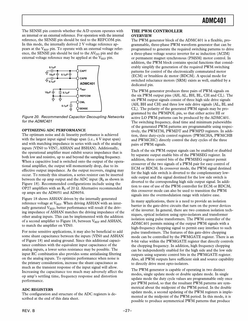
ADMC401
–27–REV. B
The SENSE pin controls whether the A/D system operates withan internal or an external reference. For operation with the internalreference, the SENSE pin should be tied to the REFCOM pin.In this mode, the internally derived 2 V voltage reference ap-pears at the VREF pin. To operate with an external voltage refer-ence, the SENSE pin should be tied to the AVDD pin and theexternal voltage reference may be applied at the VREF pin.
REFCOM
SENSE0.1F
CML
CAPB
ADMC401
CAPT
VREF
0.1F
0.1F10F
0.1F
0.1F
10F
Figure 20. Recommended Capacitor Decoupling Networksfor the ADMC401
OPTIMIZING ADC PERFORMANCEThe optimum noise and dc linearity performance is achievedwith the largest input signal voltage span (i.e., 4 V input span)and with matching impedance in series with each of the analoginputs (VIN0 to VIN7, ASHAN and BSHAN). Additionally,the operational amplifier must exhibit source impedance that isboth low and resistive, up to and beyond the sampling frequency.When a capacitive load is switched onto the output of the opera-tional amplifier, the output will momentarily drop, due to itseffective output impedance. As the output recovers, ringing mayoccur. To remedy this situation, a series resistor can be insertedbetween the op amp output and the ADC input (RS as shown inFigure 18). Recommended configurations include using theOP27 amplifiers with an RS of 20 Ω. Alternative recommendedop amps are the AD8051 and AD8054.
Figure 18 shows ASHAN driven by the internally generatedreference voltage at VREF. When driving ASHAN with an inter-nally generated VREF, better performance will result if the driv-ing impedance of ASHAN matches the driving impedance of theother analog inputs. This can be implemented with the additionof a second amplifier to Figure 18, between VREF and ASHAN,to match the amplifier on VIN0.
For noise sensitive applications, it may also be beneficial to addsome shunt capacitance between the inputs (VIN0 and ASHANof Figure 18) and analog ground. Since this additional capaci-tance combines with the equivalent input capacitance of theanalog inputs, a lower series resistance may be possible. Theinput RC combination also provides some antialiasing filteringon the analog inputs. To optimize performance when noise isthe primary consideration, increase the shunt capacitance asmuch as the transient response of the input signal will allow.Increasing the capacitance too much may adversely affect theop amp’s settling time, frequency response and distortionperformance.
ADC REGISTERSThe configuration and structure of the ADC registers is de-scribed at the end of this data sheet.
THE PWM CONTROLLEROVERVIEWThe PWM generator block of the ADMC401 is a flexible, pro-grammable, three-phase PWM waveform generator that can beprogrammed to generate the required switching patterns to drivea three-phase voltage source inverter for ac induction (ACIM)or permanent magnet synchronous (PMSM) motor control. Inaddition, the PWM block contains special functions that consid-erably simplify the generation of the required PWM switchingpatterns for control of the electronically commutated motor(ECM) or brushless dc motor (BDCM). A special mode forswitched reluctance motors (SRM) exists as well, enabled by adedicated pin.
The PWM generator produces three pairs of PWM signals onthe six PWM output pins (AH, AL, BH, BL, CH and CL). Thesix PWM output signals consist of three high side drive signals(AH, BH and CH) and three low side drive signals (AL, BL andCL). The polarity of the generated PWM signals may be pro-grammed by the PWMPOL pin, so that either active HI oractive LO PWM patterns can be produced by the ADMC401.The switching frequency, dead time and minimum pulsewidthsof the generated PWM patterns are programmable using respec-tively, the PWMTM, PWMDT and PWMPD registers. In addi-tion, three duty-cycle control registers (PWMCHA, PWMCHBand PWMCHC) directly control the duty cycles of the threepairs of PWM signals.
Each of the six PWM output signals can be enabled or disabledby separate output enable bits of the PWMSEG register. Inaddition, three control bits of the PWMSEG register permitcrossover of the two signals of a PWM pair for easy control ofECM or BDCM. In crossover mode, the PWM signal destinedfor the high side switch is diverted to the complementary low-side output and the signal destined for the low side switch isdiverted to the corresponding high side output signal. In addi-tion to ease of use of the PWM controller for ECM or BDCM,this crossover mode can also be used to transition the PWMsignals into the overmodulation range with relative ease.
In many applications, there is a need to provide an isolationbarrier in the gate-drive circuits that turn on the power devicesof the inverter. In general, there are two common isolation tech-niques, optical isolation using opto-isolators and transformerisolation using pulse transformers. The PWM controller of theADMC401 permits mixing of the output PWM signals with ahigh-frequency chopping signal to permit easy interface to suchpulse transformers. The features of this gate-drive choppingmode can be controlled by the PWMGATE register. There is an8-bit value within the PWMGATE register that directly controlsthe chopping frequency. In addition, high frequency choppingcan be independently enabled for the high side and the low sideoutputs using separate control bits in the PWMGATE register.Also, all PWM outputs have sufficient sink and source capabilityto directly drive most opto-isolators.
The PWM generator is capable of operating in two distinctmodes, single update mode or double update mode. In singleupdate mode the duty cycle values are programmable only onceper PWM period, so that the resultant PWM patterns are sym-metrical about the midpoint of the PWM period. In the doubleupdate mode, a second updating of the PWM registers is imple-mented at the midpoint of the PWM period. In this mode, it ispossible to produce asymmetrical PWM patterns that produce
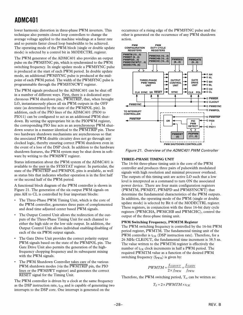
REV. B
ADMC401
–28–
lower harmonic distortion in three-phase PWM inverters. Thistechnique also permits closed loop controllers to change theaverage voltage applied to the machine windings at a faster rateand so permits faster closed loop bandwidths to be achieved.The operating mode of the PWM block (single or double updatemode) is selected by a control bit in MODECTRL register.
The PWM generator of the ADMC401 also provides an outputpulse on the PWMSYNC pin, which is synchronized to the PWMswitching frequency. In single update mode a PWMSYNC pulseis produced at the start of each PWM period. In double updatemode, an additional PWMSYNC pulse is produced at the mid-point of each PWM period. The width of the PWMSYNC pulse isprogrammable through the PWMSYNCWT register.
The PWM signals produced by the ADMC401 can be shut offin a number of different ways. First, there is a dedicated asyn-chronous PWM shutdown pin, PWMTRIP, that, when broughtLO, instantaneously places all six PWM outputs in the OFFstate (as determined by the state of the PWMPOL pin). Inaddition, each of the PIO lines of the ADMC401 (PIO0 toPIO11) can be configured to act as an additional PWM shut-down. By setting the appropriate bit in the PIOPWM register,the corresponding PIO line acts as an asynchronous PWM shut-down source in a manner identical to the PWMTRIP pin. Thesetwo hardware shutdown mechanisms are asynchronous so thatthe associated PWM disable circuitry does not go through anyclocked logic, thereby ensuring correct PWM shutdown even inthe event of a loss of the DSP clock. In addition to the hardwareshutdown features, the PWM system may be shut down in soft-ware by writing to the PWMSWT register.
Status information about the PWM system of the ADMC401 isavailable to the user in the SYSSTAT register. In particular, thestate of the PWMTRIP and PWMPOL pins is available, as wellas status bits that indicates whether operation is in the first halfor the second half of the PWM period.
A functional block diagram of the PWM controller is shown inFigure 21. The generation of the six output PWM signals onpins AH to CL is controlled by four important blocks:
• The Three-Phase PWM Timing Unit, which is the core ofthe PWM controller, generates three pairs of complementedand dead time adjusted center based PWM signals.
• The Output Control Unit allows the redirection of the out-puts of the Three-Phase Timing Unit for each channel toeither the high side or the low side output. In addition, theOutput Control Unit allows individual enabling/disabling ofeach of the six PWM output signals.
• The Gate Drive Unit provides the correct polarity outputPWM signals based on the state of the PWMPOL pin. TheGate Drive Unit also permits the generation of the high-frequency chopping frequency and its subsequent mixingwith the PWM signals.
• The PWM Shutdown Controller takes care of the variousPWM shutdown modes (via the PWMTRIP pin, the PIOlines or the PWMSWT register) and generates the correctRESET signal for the Timing Unit.
The PWM controller is driven by a clock at the same frequencyas the DSP instruction rate, tCK and is capable of generating twointerrupts to the DSP core. One interrupt is generated on the
occurrence of a rising edge of the PWMSYNC pulse and theother is generated on the occurrence of any PWM shutdownaction.
AH
PWMCHA (15…0)PWMCHB (15…0)PWMCHC (15…0)
PWMSEG(8…0)
PWMGATE(9…0)
THREE-PHASEPWM TIMING
UNIT
OUTPUTCONTROL
UNIT
CLK SYNC RESET SYNC
GATEDRIVEUNIT
CLK POL
CLKOUT
PWMTM (15…0)PWMDT (9…0)PWMPD(9…0)PWMSYNCWT(7…0)MODECTRL (6)
PWMSWT(0)
PIOPWM(11…0)
AL
BHBL
CHCL
PWMTRIP
PWMSYNC
PWMPOL
PIO0
PIO11
TO INTERRUPTCONTROLLER
PWMCONFIGURATION
REGISTERS
PWMDUTY CYCLEREGISTERS
PWMSYNC
PWMTRIP
PWM SHUTDOWN CONTROLLER
SR
PWMSR
OR PIOPWM
DETECT
Figure 21. Overview of the ADMC401 PWM Controller
THREE-PHASE TIMING UNITThe 16-bit three-phase timing unit is the core of the PWMcontroller and produces three pairs of pulsewidth modulatedsignals with high resolution and minimal processor overhead.The outputs of this timing unit are active LO such that a lowlevel is interpreted as a command to turn ON the associatedpower device. There are four main configuration registers(PWMTM, PWMDT, PWMPD and PWMSYNCWT) thatdetermine the fundamental characteristics of the PWM outputs.In addition, the operating mode of the PWM (single or doubleupdate mode) is selected by Bit 6 of the MODECTRL register.These registers, in conjunction with the three 16-bit duty cycleregisters (PWMCHA, PWMCHB and PWMCHC), control theoutput of the three-phase timing unit.
PWM Switching Frequency, PWMTM RegisterThe PWM switching frequency is controlled by the 16-bit PWMperiod register, PWMTM. The fundamental timing unit of thePWM controller is tCK (DSP instruction rate). Therefore, for a26 MHz CLKOUT, the fundamental time increment is 38.5 ns.The value written to the PWMTM register is effectively thenumber of tCK clock increments in half a PWM period. Therequired PWMTM value as a function of the desired PWMswitching frequency (fPWM) is given by:
PWMTM
ff
ff
CLKOUT
PWM
CLKIN
PWM=
×=
2
Therefore, the PWM switching period, Ts, can be written as:
T PWMTM tS CK= × ×2
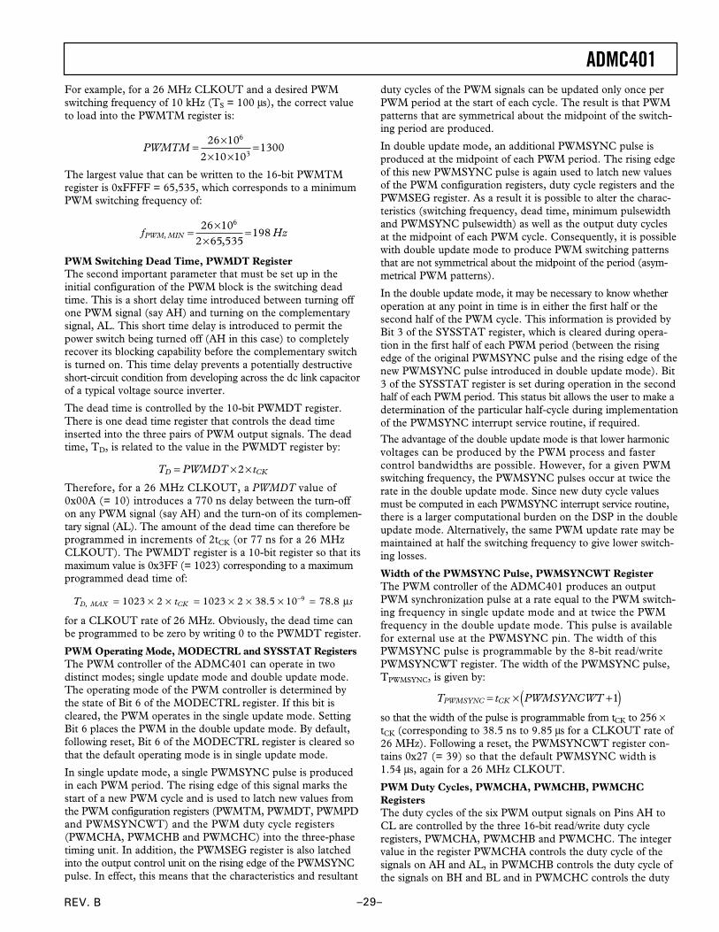
ADMC401
–29–REV. B
For example, for a 26 MHz CLKOUT and a desired PWMswitching frequency of 10 kHz (TS = 100 µs), the correct valueto load into the PWMTM register is:
PWMTM =
×× ×
=26 10
2 10 101300
6
3
The largest value that can be written to the 16-bit PWMTMregister is 0xFFFF = 65,535, which corresponds to a minimumPWM switching frequency of:
f HzPWM MIN,
,=
××
=26 10
2 65 535198
6
PWM Switching Dead Time, PWMDT RegisterThe second important parameter that must be set up in theinitial configuration of the PWM block is the switching deadtime. This is a short delay time introduced between turning offone PWM signal (say AH) and turning on the complementarysignal, AL. This short time delay is introduced to permit thepower switch being turned off (AH in this case) to completelyrecover its blocking capability before the complementary switchis turned on. This time delay prevents a potentially destructiveshort-circuit condition from developing across the dc link capacitorof a typical voltage source inverter.
The dead time is controlled by the 10-bit PWMDT register.There is one dead time register that controls the dead timeinserted into the three pairs of PWM output signals. The deadtime, TD, is related to the value in the PWMDT register by:
T PWMDT tD CK= × ×2
Therefore, for a 26 MHz CLKOUT, a PWMDT value of0x00A (= 10) introduces a 770 ns delay between the turn-offon any PWM signal (say AH) and the turn-on of its complemen-tary signal (AL). The amount of the dead time can therefore beprogrammed in increments of 2tCK (or 77 ns for a 26 MHzCLKOUT). The PWMDT register is a 10-bit register so that itsmaximum value is 0x3FF (= 1023) corresponding to a maximumprogrammed dead time of:
T t sD MAX CK,–. .= × × = × × × =1023 2 1023 2 38 5 10 78 89 µ
for a CLKOUT rate of 26 MHz. Obviously, the dead time canbe programmed to be zero by writing 0 to the PWMDT register.
PWM Operating Mode, MODECTRL and SYSSTAT RegistersThe PWM controller of the ADMC401 can operate in twodistinct modes; single update mode and double update mode.The operating mode of the PWM controller is determined bythe state of Bit 6 of the MODECTRL register. If this bit iscleared, the PWM operates in the single update mode. SettingBit 6 places the PWM in the double update mode. By default,following reset, Bit 6 of the MODECTRL register is cleared sothat the default operating mode is in single update mode.
In single update mode, a single PWMSYNC pulse is producedin each PWM period. The rising edge of this signal marks thestart of a new PWM cycle and is used to latch new values fromthe PWM configuration registers (PWMTM, PWMDT, PWMPDand PWMSYNCWT) and the PWM duty cycle registers(PWMCHA, PWMCHB and PWMCHC) into the three-phasetiming unit. In addition, the PWMSEG register is also latchedinto the output control unit on the rising edge of the PWMSYNCpulse. In effect, this means that the characteristics and resultant
duty cycles of the PWM signals can be updated only once perPWM period at the start of each cycle. The result is that PWMpatterns that are symmetrical about the midpoint of the switch-ing period are produced.
In double update mode, an additional PWMSYNC pulse isproduced at the midpoint of each PWM period. The rising edgeof this new PWMSYNC pulse is again used to latch new valuesof the PWM configuration registers, duty cycle registers and thePWMSEG register. As a result it is possible to alter the charac-teristics (switching frequency, dead time, minimum pulsewidthand PWMSYNC pulsewidth) as well as the output duty cyclesat the midpoint of each PWM cycle. Consequently, it is possiblewith double update mode to produce PWM switching patternsthat are not symmetrical about the midpoint of the period (asym-metrical PWM patterns).
In the double update mode, it may be necessary to know whetheroperation at any point in time is in either the first half or thesecond half of the PWM cycle. This information is provided byBit 3 of the SYSSTAT register, which is cleared during opera-tion in the first half of each PWM period (between the risingedge of the original PWMSYNC pulse and the rising edge of thenew PWMSYNC pulse introduced in double update mode). Bit3 of the SYSSTAT register is set during operation in the secondhalf of each PWM period. This status bit allows the user to make adetermination of the particular half-cycle during implementationof the PWMSYNC interrupt service routine, if required.
The advantage of the double update mode is that lower harmonicvoltages can be produced by the PWM process and fastercontrol bandwidths are possible. However, for a given PWMswitching frequency, the PWMSYNC pulses occur at twice therate in the double update mode. Since new duty cycle valuesmust be computed in each PWMSYNC interrupt service routine,there is a larger computational burden on the DSP in the doubleupdate mode. Alternatively, the same PWM update rate may bemaintained at half the switching frequency to give lower switch-ing losses.
Width of the PWMSYNC Pulse, PWMSYNCWT RegisterThe PWM controller of the ADMC401 produces an outputPWM synchronization pulse at a rate equal to the PWM switch-ing frequency in single update mode and at twice the PWMfrequency in the double update mode. This pulse is availablefor external use at the PWMSYNC pin. The width of thisPWMSYNC pulse is programmable by the 8-bit read/writePWMSYNCWT register. The width of the PWMSYNC pulse,TPWMSYNC, is given by:
T t PWMSYNCWTPWMSYNC CK= × +( )1
so that the width of the pulse is programmable from tCK to 256 ×tCK (corresponding to 38.5 ns to 9.85 µs for a CLKOUT rate of26 MHz). Following a reset, the PWMSYNCWT register con-tains 0x27 (= 39) so that the default PWMSYNC width is1.54 µs, again for a 26 MHz CLKOUT.
PWM Duty Cycles, PWMCHA, PWMCHB, PWMCHCRegistersThe duty cycles of the six PWM output signals on Pins AH toCL are controlled by the three 16-bit read/write duty cycleregisters, PWMCHA, PWMCHB and PWMCHC. The integervalue in the register PWMCHA controls the duty cycle of thesignals on AH and AL, in PWMCHB controls the duty cycle ofthe signals on BH and BL and in PWMCHC controls the duty
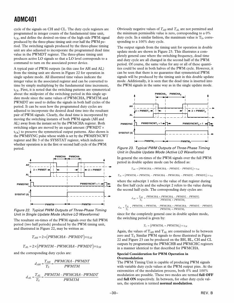
REV. B
ADMC401
–30–
cycle of the signals on CH and CL. The duty cycle registers areprogrammed in integer counts of the fundamental time unit,tCK, and define the desired on-time of the high side PWM signalproduced by the three-phase timing unit over half the PWM pe-riod. The switching signals produced by the three-phase timingunit are also adjusted to incorporate the programmed dead timevalue in the PWMDT register. The three-phase timing unitproduces active LO signals so that a LO level corresponds to acommand to turn on the associated power device.
A typical pair of PWM outputs (in this case for AH and AL)from the timing unit are shown in Figure 22 for operation insingle update mode. All illustrated time values indicate theinteger value in the associated register and can be converted totime by simply multiplying by the fundamental time increment,tCK. First, it is noted that the switching patterns are symmetricalabout the midpoint of the switching period in this single up-date mode since the same values of PWMCHA, PWMTM andPWMDT are used to define the signals in both half cycles of theperiod. It can be seen how the programmed duty cycles areadjusted to incorporate the desired dead time into the resultantpair of PWM signals. Clearly, the dead time is incorporated bymoving the switching instants of both PWM signals (AH andAL) away from the instant set by the PWMCHA register. Bothswitching edges are moved by an equal amount (PWMDT ×tCK) to preserve the symmetrical output patterns. Also shown isthe PWMSYNC pulse whose width is set by the PWMSYNCWTregister and Bit 3 of the SYSSTAT register, which indicateswhether operation is in the first or second half cycle of the PWMperiod.
PWMSYNC
AH
AL
PWMCHA PWMCHA
2 PWMDT
PWMSYNCWT + 1
2 PWMDT
SYSSTAT (3)
PWMTM PWMTM
Figure 22. Typical PWM Outputs of Three-Phase TimingUnit in Single Update Mode (Active LO Waveforms)
The resultant on-times of the PWM signals over the full PWMperiod (two half periods) produced by the PWM timing unit,and illustrated in Figure 22, may be written as:
T PWMCHA PWMDT tAH CK= ×( )×2 –
T PWMTM PWMCHA PWMDT tAL CK= ×( )×2 – –
and the corresponding duty cycles are:
d
TT
PWMCHA PWMDTPWMTM
AHAH
S= =
–
d
TT
PWMTM PWMCHA PWMDTPWMTM
ALAL
S= =
– –
Obviously negative values of TAH and TAL are not permitted andthe minimum permissible value is zero, corresponding to a 0%duty cycle. In a similar fashion, the maximum value is TS, corre-sponding to a 100% duty cycle.
The output signals from the timing unit for operation in doubleupdate mode are shown in Figure 23. This illustrates a com-pletely general case where the switching frequency, dead timeand duty cycle are all changed in the second half of the PWMperiod. Of course, the same value for any or all of these quanti-ties could be used in both halves of the PWM cycle. However, itcan be seen that there is no guarantee that symmetrical PWMsignals will be produced by the timing unit in this double updatemode. Additionally, it is seen that the dead time is inserted intothe PWM signals in the same way as in the single update mode.
PWMCHA2
2 PWMDT1 2 PWMDT2
PWMSYNCWT2 + 1
PWMCHA1
PWMTM1 PWMTM2
PWMSYNCWT1 + 1
AH
AL
PWMSYNC
SYSSTAT (3)
Figure 23. Typical PWM Outputs of Three-Phase TimingUnit in Double Update Mode (Active LO Waveforms)
In general the on-times of the PWM signals over the full PWMperiod in double update mode can be defined as:
T PWMCHA PWMCHA PWMDT PWMDT tAH CK= +( ) ×1 2 1 2– –
T PWMTM PWMTM PWMCHA PWMCHA PWMDT PWMDT tAL CK= +( ) ×1 2 1 2 1 2– – – –
where the subscript 1 refers to the value of that register duringthe first half cycle and the subscript 2 refers to the value duringthe second half cycle. The corresponding duty cycles are:
d
TT
PWMCHA PWMCHA PWMDT PWMDTPWMTM PWMTMAH
AH
S= =
++
1 2 1 2
1 2
– –
d
TT
PWMTM PWMTM PWMCHA PWMCHA PWMDT PWMDTPWMTM PWMTMAL
AL
S= =
+ ++
1 2 1 2 1 2
1 2
– – –
since for the completely general case in double update mode,the switching period is given by:
T PWMTM PWMTM tS CK= +( ) ×1 2
Again, the values of TAH and TAL are constrained to lie betweenzero and TS. Similar PWM signals to those illustrated in Figure22 and Figure 23 can be produced on the BH, BL, CH and CLoutputs by programming the PWMCHB and PWMCHC registersin a manner identical to that described for PWMCHA.
Special Consideration for PWM Operation inOvermodulationThe PWM Timing Unit is capable of producing PWM signalswith variable duty cycle values at the PWM output pins. At theextremities of the modulation process, both 0% and 100%modulation are possible. These two modes are termed full OFFand full ON respectively. In between, for other duty cycle val-ues, the operation is termed normal modulation.
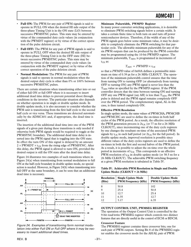
ADMC401
–31–REV. B
• Full ON: The PWM for any pair of PWM signals is said tooperate in FULL ON when the desired HI side output of thethree-phase Timing Unit is in the ON state (LO) betweensuccessive PWMSYNC pulses. This state may be entered byvirtue of the commanded duty cycle values (in conjunctionwith the PWMDT register) or by virtue of the correct opera-tion of the pulse deletion circuit.
• Full OFF: The PWM for any pair of PWM signals is said tooperate in FULL OFF when the desired HI side output ofthe three-phase Timing Unit is in the OFF state (HI) be-tween successive PWMSYNC pulses. This state may beentered by virtue of the commanded duty cycle values (inconjunction with the PWMDT register) or by virtue of thecorrect operation of the pulse deletion circuit.
• Normal Modulation: The PWM for any pair of PWMsignals is said to operate in normal modulation when thedesired output duty cycle is other than 0% or 100% betweensuccessive PWMSYNC pulses.
There are certain situations when transitioning either into or outof either full ON or full OFF where it is necessary to insertadditional dead time delays to prevent potential shoot throughconditions in the inverter. The particular situation also dependson whether operation is in single or double update mode. Indouble update mode, it is also necessary to consider whether thePWM unit is transitioning from the first half cycle to the secondhalf cycle or vice versa. These transitions are detected automati-cally by the ADMC401 and, if appropriate, the dead time isinserted.
The insertion of the additional dead time into one of the PWMsignals of a given pair during these transitions is only needed ifotherwise both PWM signals would be required to toggle at thePWMSYNC boundary. The additional dead time delay is in-serted into the PWM signal that is toggling into the ON state.In effect the turn ON of this signal is delayed by an amount2 × PWMDT × tCK from the rising edge of PWMSYNC. Afterthis delay, the PWM signal is allowed to turn ON, provided thedesired output is still the ON state after the dead time delay.
Figure 24 illustrates two examples of such transitions where inFigure 24(a) when transitioning from normal modulation to fullON at the half cycle boundary in double update mode, no specialaction is needed. However, in Figure 24(b) when transitioning intofull OFF at the same boundary, it can be seen that an additionaldead time is necessary.
2 PWMDT
PWMCHA1
FULL ONAH
AL
2 PWMDT
FULL OFF
AH
AL
(a)
(b)
PWMTM PWMTM
DEAD TIME INSERTED
Figure 24. Examples of transitioning form normal modu-lation into either Full ON or Full OFF where it may be nec-essary to insert additional dead times.
Minimum Pulsewidth, PWMPD RegisterIn many power converter switching applications, it is desirableto eliminate PWM switching signals below a certain width. Ittakes a certain finite time to both turn on and turn off powersemiconductor devices. Therefore, if the width of any of thePWM signals goes below some minimum value, it may be desir-able to completely eliminate the PWM switching for that par-ticular cycle. The allowable minimum pulsewidth for any of thesix PWM outputs that can be produced by the PWM controllermay be programmed using the 10-bit PWMPD register. Theminimum pulsewidth, TMIN, is programmed in increments oftCK as:
T PWMPD tMIN CK= ×
so that a PWMPD value of 0x00A defines a permissible mini-mum on time of 0.39 µs for a 26 MHz CLKOUT. The opera-tion of the minimum pulsewidth control ensures that the timefrom turning ON to turning OFF (or alternatively from turningOFF to turning ON) any PWM signal is never less than theTMIN value as specified by the PWMPD register. If the PWMcontroller detects that the time between turning ON and turningOFF any one PWM signal (say AH) is less than TMIN, the PWMpulse is deleted and the PWM signal remains completely OFFover the PWM period. The complementary signal, AL in thiscase, is then turned completely ON.
Effective PWM ResolutionIn single update mode, the same values of PWMCHA, PWMCHBand PWMCHC are used to define the on-times in both halfcycles of the PWM period. As a result, the effective resolution ofthe PWM generation process is 2tCK (or 77 ns for a 26 MHzCLKOUT), since incrementing one of the duty cycle registersby one changes the resultant on-time of the associated PWMsignals by tCK in each half period (or 2tCK for the full period). Indouble update mode, improved resolution is possible sincedifferent values of the duty cycles registers are used to define theon-times in both the first and second halves of the PWM period.As a result, it is possible to adjust the on-time over the wholeperiod in increments of tCK. This corresponds to an effectivePWM resolution of tCK in double update mode (or 38.5 ns for a26 MHz CLKOUT). The achievable PWM switching frequencyat a given PWM resolution is tabulated in Table IV.
Table IV. Achievable PWM Resolution in Single and DoubleUpdate Modes (CLKOUT = 26 MHz)
Resolution Single Update Mode Double Update Mode(Bits) PWM Frequency (kHz) PWM Frequency (kHz)
8 50.8 1029 25.4 50.810 12.7 25.411 6.35 12.712 3.17 6.35
OUTPUT CONTROL UNIT, PWMSEG REGISTERThe operation of the Output Control Unit is controlled by the9-bit read/write PWMSEG register which controls two distinctfeatures that are directly useful in the control of ECM or BDCM.
Crossover FeatureThe PWMSEG register contains three crossover bits; one foreach pair of PWM outputs. Setting Bit 8 of the PWMSEG regis-ter enables the crossover mode for the AH/AL pair of PWM
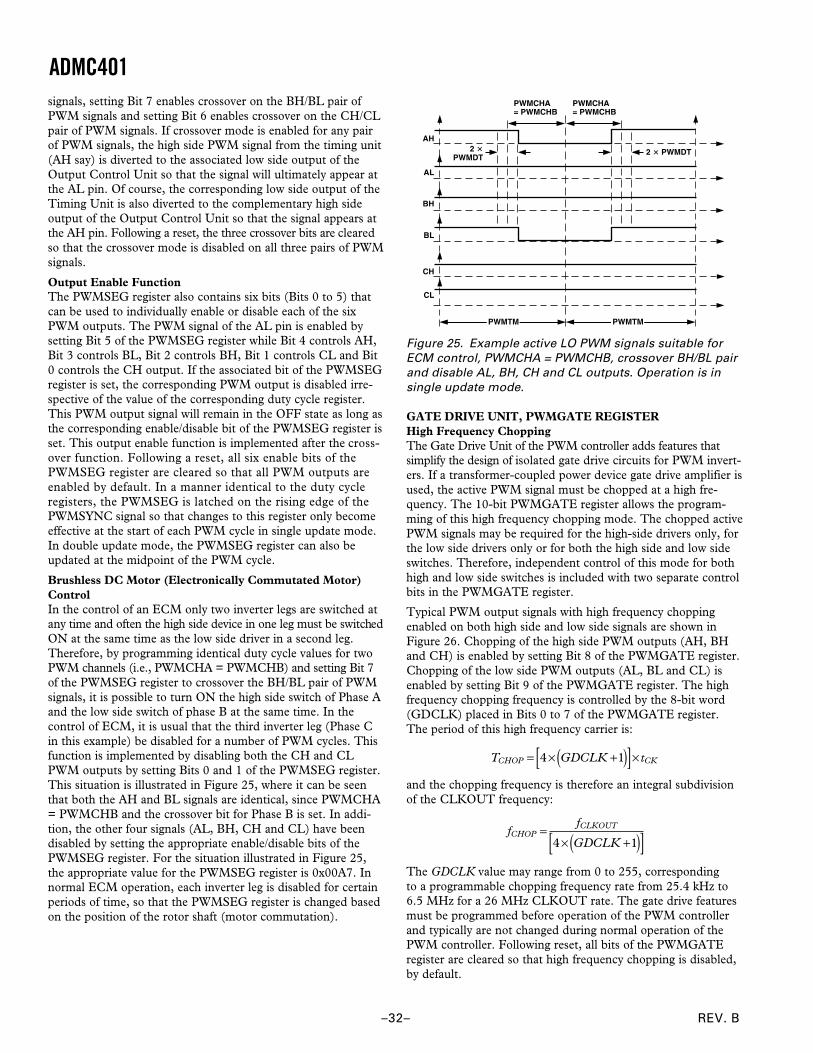
REV. B
ADMC401
–32–
signals, setting Bit 7 enables crossover on the BH/BL pair ofPWM signals and setting Bit 6 enables crossover on the CH/CLpair of PWM signals. If crossover mode is enabled for any pairof PWM signals, the high side PWM signal from the timing unit(AH say) is diverted to the associated low side output of theOutput Control Unit so that the signal will ultimately appear atthe AL pin. Of course, the corresponding low side output of theTiming Unit is also diverted to the complementary high sideoutput of the Output Control Unit so that the signal appears atthe AH pin. Following a reset, the three crossover bits are clearedso that the crossover mode is disabled on all three pairs of PWMsignals.
Output Enable FunctionThe PWMSEG register also contains six bits (Bits 0 to 5) thatcan be used to individually enable or disable each of the sixPWM outputs. The PWM signal of the AL pin is enabled bysetting Bit 5 of the PWMSEG register while Bit 4 controls AH,Bit 3 controls BL, Bit 2 controls BH, Bit 1 controls CL and Bit0 controls the CH output. If the associated bit of the PWMSEGregister is set, the corresponding PWM output is disabled irre-spective of the value of the corresponding duty cycle register.This PWM output signal will remain in the OFF state as long asthe corresponding enable/disable bit of the PWMSEG register isset. This output enable function is implemented after the cross-over function. Following a reset, all six enable bits of thePWMSEG register are cleared so that all PWM outputs areenabled by default. In a manner identical to the duty cycleregisters, the PWMSEG is latched on the rising edge of thePWMSYNC signal so that changes to this register only becomeeffective at the start of each PWM cycle in single update mode.In double update mode, the PWMSEG register can also beupdated at the midpoint of the PWM cycle.
Brushless DC Motor (Electronically Commutated Motor)ControlIn the control of an ECM only two inverter legs are switched atany time and often the high side device in one leg must be switchedON at the same time as the low side driver in a second leg.Therefore, by programming identical duty cycle values for twoPWM channels (i.e., PWMCHA = PWMCHB) and setting Bit 7of the PWMSEG register to crossover the BH/BL pair of PWMsignals, it is possible to turn ON the high side switch of Phase Aand the low side switch of phase B at the same time. In thecontrol of ECM, it is usual that the third inverter leg (Phase Cin this example) be disabled for a number of PWM cycles. Thisfunction is implemented by disabling both the CH and CLPWM outputs by setting Bits 0 and 1 of the PWMSEG register.This situation is illustrated in Figure 25, where it can be seenthat both the AH and BL signals are identical, since PWMCHA= PWMCHB and the crossover bit for Phase B is set. In addi-tion, the other four signals (AL, BH, CH and CL) have beendisabled by setting the appropriate enable/disable bits of thePWMSEG register. For the situation illustrated in Figure 25,the appropriate value for the PWMSEG register is 0x00A7. Innormal ECM operation, each inverter leg is disabled for certainperiods of time, so that the PWMSEG register is changed basedon the position of the rotor shaft (motor commutation).
AH
AL
BH
BL
CH
CL
PWMTM PWMTM
PWMCHA= PWMCHB
PWMCHA= PWMCHB
2 PWMDT
2 PWMDT
Figure 25. Example active LO PWM signals suitable forECM control, PWMCHA = PWMCHB, crossover BH/BL pairand disable AL, BH, CH and CL outputs. Operation is insingle update mode.
GATE DRIVE UNIT, PWMGATE REGISTERHigh Frequency ChoppingThe Gate Drive Unit of the PWM controller adds features thatsimplify the design of isolated gate drive circuits for PWM invert-ers. If a transformer-coupled power device gate drive amplifier isused, the active PWM signal must be chopped at a high fre-quency. The 10-bit PWMGATE register allows the program-ming of this high frequency chopping mode. The chopped activePWM signals may be required for the high-side drivers only, forthe low side drivers only or for both the high side and low sideswitches. Therefore, independent control of this mode for bothhigh and low side switches is included with two separate controlbits in the PWMGATE register.
Typical PWM output signals with high frequency choppingenabled on both high side and low side signals are shown inFigure 26. Chopping of the high side PWM outputs (AH, BHand CH) is enabled by setting Bit 8 of the PWMGATE register.Chopping of the low side PWM outputs (AL, BL and CL) isenabled by setting Bit 9 of the PWMGATE register. The highfrequency chopping frequency is controlled by the 8-bit word(GDCLK) placed in Bits 0 to 7 of the PWMGATE register.The period of this high frequency carrier is:
T GDCLK tCHOP CK= × +( )[ ]×4 1
and the chopping frequency is therefore an integral subdivisionof the CLKOUT frequency:
ff
GDCLKCHOP
CLKOUT=× +( )[ ]4 1
The GDCLK value may range from 0 to 255, correspondingto a programmable chopping frequency rate from 25.4 kHz to6.5 MHz for a 26 MHz CLKOUT rate. The gate drive featuresmust be programmed before operation of the PWM controllerand typically are not changed during normal operation of thePWM controller. Following reset, all bits of the PWMGATEregister are cleared so that high frequency chopping is disabled,by default.
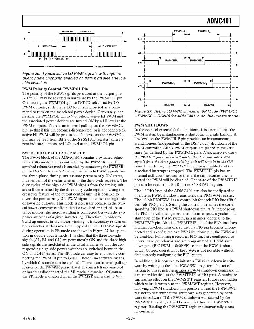
ADMC401
–33–REV. B
PWMTM PWMTM
[4 (GDCLK+1)]
2 PWMDT 2 PWMDT
PWMCHA PWMCHA
AH
AL
Figure 26. Typical active LO PWM signals with high fre-quency gate chopping enabled on both high side and lowside switches.
PWM Polarity Control, PWMPOL PinThe polarity of the PWM signals produced at the output pinsAH to CL may be selected in hardware by the PWMPOL pin.Connecting the PWMPOL pin to DGND selects active LOPWM outputs, such that a LO level is interpreted as a com-mand to turn on the associated power device. Conversely, con-necting the PWMPOL pin to VDD selects active HI PWM andthe associated power devices are turned ON by a HI level at thePWM outputs. There is an internal pull-up on the PWMPOLpin, so that if this pin becomes disconnected (or is not connected),active HI PWM will be produced. The level on the PWMPOLpin may be read from Bit 2 of the SYSSTAT register, where azero indicates a measured LO level at the PWMPOL pin.
SWITCHED RELUCTANCE MODEThe PWM block of the ADMC401 contains a switched reluc-tance (SR) mode that is controlled by the PWMSR pin. Theswitched reluctance mode is enabled by connecting the PWMSRpin to DGND. In this SR mode, the low side PWM signals fromthe three-phase timing unit assume permanently ON states,independent of the value written to the duty-cycle registers. Theduty cycles of the high side PWM signals from the timing unitare still determined by the three duty cycle registers. Using thecrossover feature of the output control unit, it is possible todivert the permanently ON PWM signals to either the high-sideor low-side outputs. This mode is necessary because in the typi-cal power converter configuration for switched or variable reluc-tance motors, the motor winding is connected between the twopower switches of a given inverter leg. Therefore, in order tobuild up current in the motor winding, it is necessary to turn onboth switches at the same time. Typical active LO PWM signalsduring operation in SR mode are shown in Figure 27 for opera-tion in double update mode. It is clear that the three low-sidesignals (AL, BL and CL) are permanently ON and the three highside signals are modulated in the usual manner so that the cor-responding high side power switches are switched between theON and OFF states. The SR mode can only be enabled by con-necting the PWMSR pin to GND. There is no software meansby which this mode can be enabled. There is an internal pull-upresistor on the PWMSR pin so that if this pin is left unconnectedor becomes disconnected the SR mode is disabled. Of course,the SR mode is disabled when the PWMSR pin is tied to VDD.
PWMCHA1
PWMTM
AH
AL
BH
CH
BL
CL
PWMCHA2
PWMCHB2PWMCHB1
PWMCHC2PWMCHC1
PWMTM
Figure 27. Active LO PWM signals in SR Mode (PWMPOL= PWMSR = DGND) for ADMC401 in double update mode.
PWM SHUTDOWNIn the event of external fault conditions, it is essential that thePWM system be instantaneously shutdown in a safe fashion. Alow level on the PWMTRIP pin provides an instantaneous,asynchronous (independent of the DSP clock) shutdown of thePWM controller. All six PWM outputs are placed in the OFFstate (as defined by the PWMPOL pin). Note, however, whenthe PWMSR pin is in the SR mode, the three low side PWMsignals from the three-phase timing unit will remain in the ONstate. In addition, the PWMSYNC pulse is disabled and theassociated interrupt is stopped. The PWMTRIP pin has aninternal pull-down resistor so that if the pin becomes uncon-nected the PWM will be disabled. The state of the PWMTRIPpin can be read from Bit 0 of the SYSSTAT register.
The 12 PIO lines of the ADMC401 can also be configured tooperate as PWM shutdown pins using the PIOPWM register.The 12-bit PIOPWM has a control bit for each PIO line (Bit 0controls PIO0, etc.). Setting the control bit enables the corre-sponding PIO line as a PWM shutdown pin. A falling edge onthe PIO line will then generate an instantaneous, asynchronousshutdown of the PWM system, in a manner identical to thePWMTRIP pin. Also like PWMTRIP, all of the PIO lines haveinternal pull-down resistors, so that if a PIO pin becomes uncon-nected and is configured as a PWM shutdown pin, the PWM willbe disabled. Following a reset, all PIO lines are configured asinputs, have pull-downs and are programmed as PWM shutdown pins (PIOPWM = 0x0FFF) so that the PWM is shut-down. Correct operation of the PWM is not possible withoutfirst correctly configuring the PIO system.
In addition, it is possible to initiate a PWM shutdown in soft-ware by writing to the 1-bit PWMSWT register. The act ofwriting to this register generates a PWM shutdown command ina manner identical to the PWMTRIP or PIO pins. A hardwaretrip has no effect on the PWMSWT register. It does not matterwhich value is written to the PWMSWT register. However,following a PWM shutdown, it is possible to read the PWMSWTregister to determine if the shutdown was generated by hard-ware or software. If the PWM shutdown was caused by thePWMSWT register, a 1 will be read back from the PWMSWTregister. Reading the PWMSWT register automatically clearsits contents.
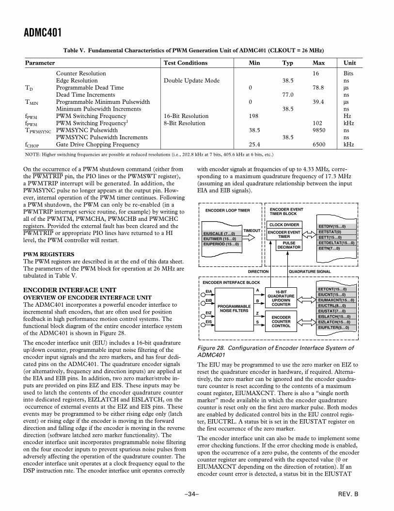
REV. B
ADMC401
–34–
On the occurrence of a PWM shutdown command (either fromthe PWMTRIP pin, the PIO lines or the PWMSWT register),a PWMTRIP interrupt will be generated. In addition, thePWMSYNC pulse no longer appears at the output pin. How-ever, internal operation of the PWM timer continues. Followinga PWM shutdown, the PWM can only be re-enabled (in aPWMTRIP interrupt service routine, for example) by writing toall of the PWMTM, PWMCHA, PWMCHB and PWMCHCregisters. Provided the external fault has been cleared and thePWMTRIP or appropriate PIO lines have returned to a HIlevel, the PWM controller will restart.
PWM REGISTERSThe PWM registers are described in at the end of this data sheet.The parameters of the PWM block for operation at 26 MHz aretabulated in Table V.
ENCODER INTERFACE UNITOVERVIEW OF ENCODER INTERFACE UNITThe ADMC401 incorporates a powerful encoder interface toincremental shaft encoders, that are often used for positionfeedback in high performance motion control systems. Thefunctional block diagram of the entire encoder interface systemof the ADMC401 is shown in Figure 28.
The encoder interface unit (EIU) includes a 16-bit quadratureup/down counter, programmable input noise filtering of theencoder input signals and the zero markers, and has four dedi-cated pins on the ADMC401. The quadrature encoder signals(or alternatively, frequency and direction inputs) are applied atthe EIA and EIB pins. In addition, two zero marker/strobe in-puts are provided on pins EIZ and EIS. These inputs may beused to latch the contents of the encoder quadrature counterinto dedicated registers, EIZLATCH and EISLATCH, on the occurrence of external events at the EIZ and EIS pins. Theseevents may be programmed to be either rising edge only (latchevent) or rising edge if the encoder is moving in the forwarddirection and falling edge if the encoder is moving in the reversedirection (software latched zero marker functionality). Theencoder interface unit incorporates programmable noise filteringon the four encoder inputs to prevent spurious noise pulses fromadversely affecting the operation of the quadrature counter. Theencoder interface unit operates at a clock frequency equal to theDSP instruction rate. The encoder interface unit operates correctly
with encoder signals at frequencies of up to 4.33 MHz, corre-sponding to a maximum quadrature frequency of 17.3 MHz(assuming an ideal quadrature relationship between the inputEIA and EIB signals).
EETCNT(15…0)EIUCNT(15…0)EIUMAXCNT(15…0)EIUCTRL(8…0)EIUSTAT(7…0)EISLATCH(15…0)EIZLATCH(15…0)EIUFILTER(5…0)
PULSEDECIMATOR
CLOCK DIVIDER
ENCODER EVENTTIMER
QUADRATURE SIGNAL
ENCODER INTERFACE BLOCK
ENCODER LOOP TIMER
TIMEOUT
DIRECTION
ENCODER EVENTTIMER BLOCK
EETDIV(15…0)EETSTAT(0)EETT(15…0)EETDELTAT(15…0)EETN(7…0)
EIUSCALE (7…0)EIUTIMER (15…0)EIUPERIOD (15…0)
EIA 16-BITQUADRATURE
UP/DOWNCOUNTER
ENCODERCOUNTERCONTROL
EIB
EIZ
B
A
EIS
Z
S
PROGRAMMABLENOISE FILTERS
Figure 28. Configuration of Encoder Interface System ofADMC401
The EIU may be programmed to use the zero marker on EIZ toreset the quadrature encoder in hardware, if required. Alterna-tively, the zero marker can be ignored and the encoder quadra-ture counter is reset according to the contents of a maximumcount register, EIUMAXCNT. There is also a “single northmarker” mode available in which the encoder quadraturecounter is reset only on the first zero marker pulse. Both modesare enabled by dedicated control bits in the EIU control regis-ter, EIUCTRL. A status bit is set in the EIUSTAT register onthe first occurrence of the zero marker.
The encoder interface unit can also be made to implement someerror checking functions. If the error checking mode is enabled,upon the occurrence of a zero pulse, the contents of the encodercounter register are compared with the expected value (0 orEIUMAXCNT depending on the direction of rotation). If anencoder count error is detected, a status bit in the EIUSTAT
Table V. Fundamental Characteristics of PWM Generation Unit of ADMC401 (CLKOUT = 26 MHz)
Parameter Test Conditions Min Typ Max Unit
Counter Resolution 16 BitsEdge Resolution Double Update Mode 38.5 ns
TD Programmable Dead Time 0 78.8 µsDead Time Increments 77.0 ns
TMIN Programmable Minimum Pulsewidth 0 39.4 µsMinimum Pulsewidth Increments 38.5 ns
fPWM PWM Switching Frequency 16-Bit Resolution 198 HzfPWM PWM Switching Frequency1 8-Bit Resolution 102 kHzTPWMSYNC PWMSYNC Pulsewidth 38.5 9850 ns
PWMSYNC Pulsewidth Increments 38.5 nsfCHOP Gate Drive Chopping Frequency 25.4 6500 kHz
NOTE: Higher switching frequencies are possible at reduced resolutions (i.e., 202.8 kHz at 7 bits, 405.6 kHz at 6 bits, etc.)
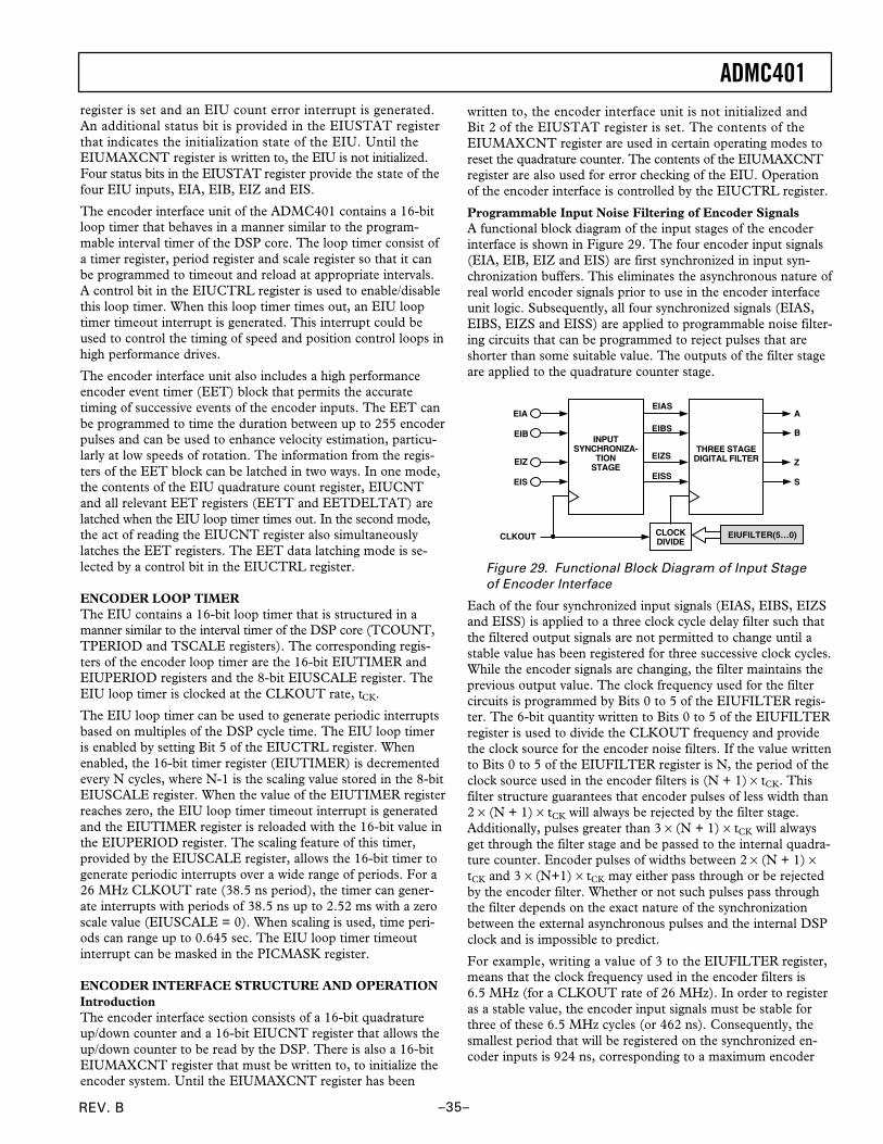
ADMC401
–35–REV. B
register is set and an EIU count error interrupt is generated.An additional status bit is provided in the EIUSTAT registerthat indicates the initialization state of the EIU. Until theEIUMAXCNT register is written to, the EIU is not initialized.Four status bits in the EIUSTAT register provide the state of thefour EIU inputs, EIA, EIB, EIZ and EIS.
The encoder interface unit of the ADMC401 contains a 16-bitloop timer that behaves in a manner similar to the program-mable interval timer of the DSP core. The loop timer consist ofa timer register, period register and scale register so that it canbe programmed to timeout and reload at appropriate intervals.A control bit in the EIUCTRL register is used to enable/disablethis loop timer. When this loop timer times out, an EIU looptimer timeout interrupt is generated. This interrupt could beused to control the timing of speed and position control loops inhigh performance drives.
The encoder interface unit also includes a high performanceencoder event timer (EET) block that permits the accuratetiming of successive events of the encoder inputs. The EET canbe programmed to time the duration between up to 255 encoderpulses and can be used to enhance velocity estimation, particu-larly at low speeds of rotation. The information from the regis-ters of the EET block can be latched in two ways. In one mode,the contents of the EIU quadrature count register, EIUCNTand all relevant EET registers (EETT and EETDELTAT) arelatched when the EIU loop timer times out. In the second mode,the act of reading the EIUCNT register also simultaneouslylatches the EET registers. The EET data latching mode is se-lected by a control bit in the EIUCTRL register.
ENCODER LOOP TIMERThe EIU contains a 16-bit loop timer that is structured in amanner similar to the interval timer of the DSP core (TCOUNT,TPERIOD and TSCALE registers). The corresponding regis-ters of the encoder loop timer are the 16-bit EIUTIMER andEIUPERIOD registers and the 8-bit EIUSCALE register. TheEIU loop timer is clocked at the CLKOUT rate, tCK.
The EIU loop timer can be used to generate periodic interruptsbased on multiples of the DSP cycle time. The EIU loop timeris enabled by setting Bit 5 of the EIUCTRL register. Whenenabled, the 16-bit timer register (EIUTIMER) is decrementedevery N cycles, where N-1 is the scaling value stored in the 8-bitEIUSCALE register. When the value of the EIUTIMER registerreaches zero, the EIU loop timer timeout interrupt is generatedand the EIUTIMER register is reloaded with the 16-bit value inthe EIUPERIOD register. The scaling feature of this timer,provided by the EIUSCALE register, allows the 16-bit timer togenerate periodic interrupts over a wide range of periods. For a26 MHz CLKOUT rate (38.5 ns period), the timer can gener-ate interrupts with periods of 38.5 ns up to 2.52 ms with a zeroscale value (EIUSCALE = 0). When scaling is used, time peri-ods can range up to 0.645 sec. The EIU loop timer timeoutinterrupt can be masked in the PICMASK register.
ENCODER INTERFACE STRUCTURE AND OPERATIONIntroductionThe encoder interface section consists of a 16-bit quadratureup/down counter and a 16-bit EIUCNT register that allows theup/down counter to be read by the DSP. There is also a 16-bitEIUMAXCNT register that must be written to, to initialize theencoder system. Until the EIUMAXCNT register has been
written to, the encoder interface unit is not initialized andBit 2 of the EIUSTAT register is set. The contents of theEIUMAXCNT register are used in certain operating modes toreset the quadrature counter. The contents of the EIUMAXCNTregister are also used for error checking of the EIU. Operationof the encoder interface is controlled by the EIUCTRL register.
Programmable Input Noise Filtering of Encoder SignalsA functional block diagram of the input stages of the encoderinterface is shown in Figure 29. The four encoder input signals(EIA, EIB, EIZ and EIS) are first synchronized in input syn-chronization buffers. This eliminates the asynchronous nature ofreal world encoder signals prior to use in the encoder interfaceunit logic. Subsequently, all four synchronized signals (EIAS,EIBS, EIZS and EISS) are applied to programmable noise filter-ing circuits that can be programmed to reject pulses that areshorter than some suitable value. The outputs of the filter stageare applied to the quadrature counter stage.
EIA
EIB
EIZ
EIS
CLKOUT CLOCKDIVIDE
EIUFILTER(5…0)
EIAS
EIBS
EIZS
EISS
A
B
Z
S
THREE STAGEDIGITAL FILTER
INPUTSYNCHRONIZA-
TIONSTAGE
Figure 29. Functional Block Diagram of Input Stageof Encoder Interface
Each of the four synchronized input signals (EIAS, EIBS, EIZSand EISS) is applied to a three clock cycle delay filter such thatthe filtered output signals are not permitted to change until astable value has been registered for three successive clock cycles.While the encoder signals are changing, the filter maintains theprevious output value. The clock frequency used for the filtercircuits is programmed by Bits 0 to 5 of the EIUFILTER regis-ter. The 6-bit quantity written to Bits 0 to 5 of the EIUFILTERregister is used to divide the CLKOUT frequency and providethe clock source for the encoder noise filters. If the value writtento Bits 0 to 5 of the EIUFILTER register is N, the period of theclock source used in the encoder filters is (N + 1) × tCK. Thisfilter structure guarantees that encoder pulses of less width than2 × (N + 1) × tCK will always be rejected by the filter stage.Additionally, pulses greater than 3 × (N + 1) × tCK will alwaysget through the filter stage and be passed to the internal quadra-ture counter. Encoder pulses of widths between 2 × (N + 1) ×tCK and 3 × (N+1) × tCK may either pass through or be rejectedby the encoder filter. Whether or not such pulses pass throughthe filter depends on the exact nature of the synchronizationbetween the external asynchronous pulses and the internal DSPclock and is impossible to predict.
For example, writing a value of 3 to the EIUFILTER register,means that the clock frequency used in the encoder filters is6.5 MHz (for a CLKOUT rate of 26 MHz). In order to registeras a stable value, the encoder input signals must be stable forthree of these 6.5 MHz cycles (or 462 ns). Consequently, thesmallest period that will be registered on the synchronized en-coder inputs is 924 ns, corresponding to a maximum encoder
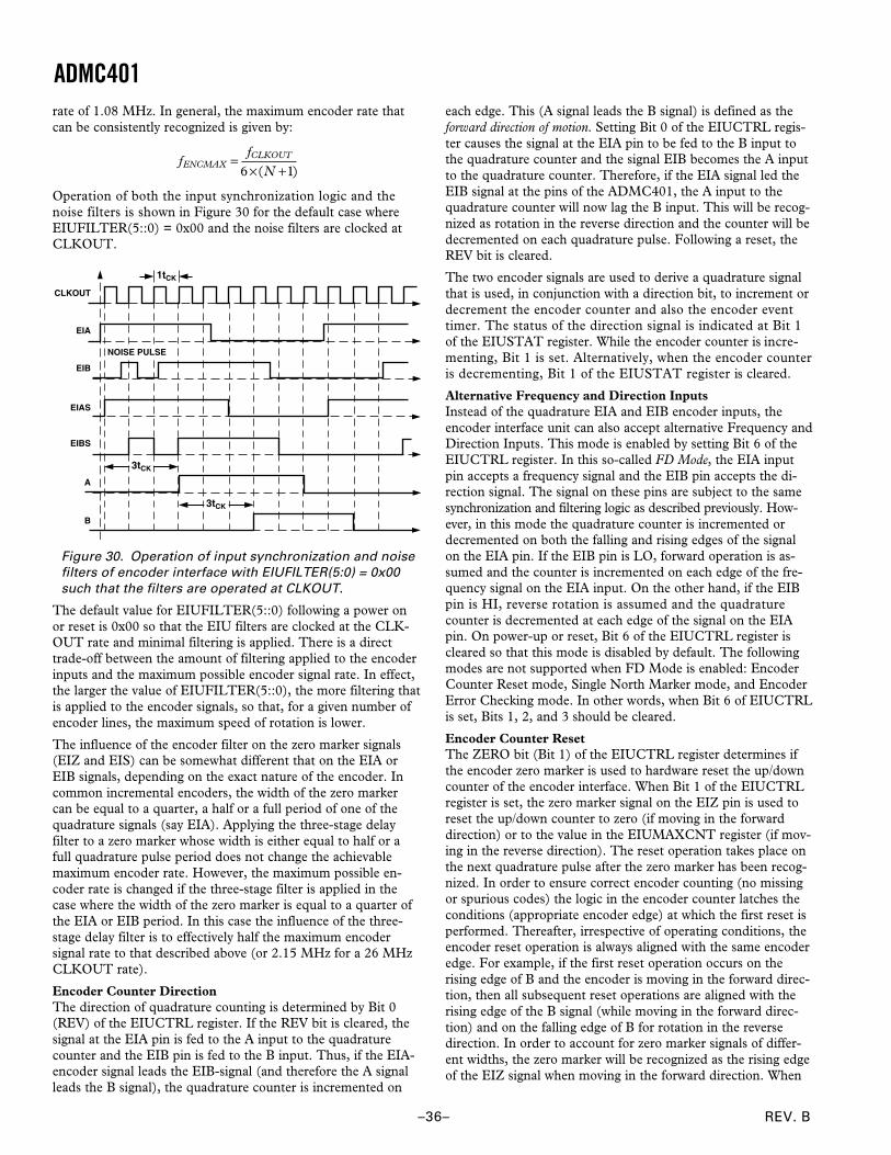
REV. B
ADMC401
–36–
rate of 1.08 MHz. In general, the maximum encoder rate thatcan be consistently recognized is given by:
f
fN
ENCMAXCLKOUT=× +6 1( )
Operation of both the input synchronization logic and thenoise filters is shown in Figure 30 for the default case whereEIUFILTER(5::0) = 0x00 and the noise filters are clocked atCLKOUT.
CLKOUT
EIA
EIB
EIAS
EIBS
A
B
3tCK
3tCK
NOISE PULSE
1tCK
Figure 30. Operation of input synchronization and noisefilters of encoder interface with EIUFILTER(5:0) = 0x00such that the filters are operated at CLKOUT.
The default value for EIUFILTER(5::0) following a power onor reset is 0x00 so that the EIU filters are clocked at the CLK-OUT rate and minimal filtering is applied. There is a directtrade-off between the amount of filtering applied to the encoderinputs and the maximum possible encoder signal rate. In effect,the larger the value of EIUFILTER(5::0), the more filtering thatis applied to the encoder signals, so that, for a given number ofencoder lines, the maximum speed of rotation is lower.
The influence of the encoder filter on the zero marker signals(EIZ and EIS) can be somewhat different that on the EIA orEIB signals, depending on the exact nature of the encoder. Incommon incremental encoders, the width of the zero markercan be equal to a quarter, a half or a full period of one of thequadrature signals (say EIA). Applying the three-stage delayfilter to a zero marker whose width is either equal to half or afull quadrature pulse period does not change the achievablemaximum encoder rate. However, the maximum possible en-coder rate is changed if the three-stage filter is applied in thecase where the width of the zero marker is equal to a quarter ofthe EIA or EIB period. In this case the influence of the three-stage delay filter is to effectively half the maximum encodersignal rate to that described above (or 2.15 MHz for a 26 MHzCLKOUT rate).
Encoder Counter DirectionThe direction of quadrature counting is determined by Bit 0(REV) of the EIUCTRL register. If the REV bit is cleared, thesignal at the EIA pin is fed to the A input to the quadraturecounter and the EIB pin is fed to the B input. Thus, if the EIA-encoder signal leads the EIB-signal (and therefore the A signalleads the B signal), the quadrature counter is incremented on
each edge. This (A signal leads the B signal) is defined as theforward direction of motion. Setting Bit 0 of the EIUCTRL regis-ter causes the signal at the EIA pin to be fed to the B input tothe quadrature counter and the signal EIB becomes the A inputto the quadrature counter. Therefore, if the EIA signal led theEIB signal at the pins of the ADMC401, the A input to thequadrature counter will now lag the B input. This will be recog-nized as rotation in the reverse direction and the counter will bedecremented on each quadrature pulse. Following a reset, theREV bit is cleared.
The two encoder signals are used to derive a quadrature signalthat is used, in conjunction with a direction bit, to increment ordecrement the encoder counter and also the encoder eventtimer. The status of the direction signal is indicated at Bit 1of the EIUSTAT register. While the encoder counter is incre-menting, Bit 1 is set. Alternatively, when the encoder counteris decrementing, Bit 1 of the EIUSTAT register is cleared.
Alternative Frequency and Direction InputsInstead of the quadrature EIA and EIB encoder inputs, theencoder interface unit can also accept alternative Frequency andDirection Inputs. This mode is enabled by setting Bit 6 of theEIUCTRL register. In this so-called FD Mode, the EIA inputpin accepts a frequency signal and the EIB pin accepts the di-rection signal. The signal on these pins are subject to the samesynchronization and filtering logic as described previously. How-ever, in this mode the quadrature counter is incremented ordecremented on both the falling and rising edges of the signalon the EIA pin. If the EIB pin is LO, forward operation is as-sumed and the counter is incremented on each edge of the fre-quency signal on the EIA input. On the other hand, if the EIBpin is HI, reverse rotation is assumed and the quadraturecounter is decremented at each edge of the signal on the EIApin. On power-up or reset, Bit 6 of the EIUCTRL register iscleared so that this mode is disabled by default. The followingmodes are not supported when FD Mode is enabled: EncoderCounter Reset mode, Single North Marker mode, and EncoderError Checking mode. In other words, when Bit 6 of EIUCTRLis set, Bits 1, 2, and 3 should be cleared.
Encoder Counter ResetThe ZERO bit (Bit 1) of the EIUCTRL register determines ifthe encoder zero marker is used to hardware reset the up/downcounter of the encoder interface. When Bit 1 of the EIUCTRLregister is set, the zero marker signal on the EIZ pin is used toreset the up/down counter to zero (if moving in the forwarddirection) or to the value in the EIUMAXCNT register (if mov-ing in the reverse direction). The reset operation takes place onthe next quadrature pulse after the zero marker has been recog-nized. In order to ensure correct encoder counting (no missingor spurious codes) the logic in the encoder counter latches theconditions (appropriate encoder edge) at which the first reset isperformed. Thereafter, irrespective of operating conditions, theencoder reset operation is always aligned with the same encoderedge. For example, if the first reset operation occurs on therising edge of B and the encoder is moving in the forward direc-tion, then all subsequent reset operations are aligned with therising edge of the B signal (while moving in the forward direc-tion) and on the falling edge of B for rotation in the reversedirection. In order to account for zero marker signals of differ-ent widths, the zero marker will be recognized as the rising edgeof the EIZ signal when moving in the forward direction. When
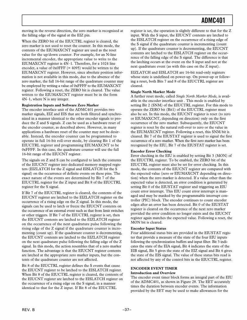
ADMC401
–37–REV. B
moving in the reverse direction, the zero marker is recognized atthe falling edge of the signal at the EIZ pin.
When the ZERO bit of the EIUCTRL register is cleared, thezero marker is not used to reset the counter. In this mode, thecontents of the EIUMAXCNT register are used as the resetvalue for the up/down counter. For example, for an N-lineincremental encoder, the appropriate value to write to theEIUMAXCNT register is 4N–1. Therefore, for a 1024 lineencoder, a value of 0x0FFF (= 4095) would be written to theEIUMAXCNT register. However, since absolute position infor-mation is not available in this mode, due to the absence of thezero marker, the full 16-bit range of the quadrature counter maybe employed by writing a value of 0xFFFF to the EIUMAXCNTregister. Following a reset, the ZERO bit is cleared. The valuewritten to the EIUMAXCNT register must be in the form4N–1, where N is any integer.
Registration Inputs and Software Zero MarkerThe encoder interface unit of the ADMC401 provides twomarker signals, EIZ and EIS that are both filtered and synchro-nized in a manner identical to the other encoder signals to pro-duce the Z and S signals. Z can be used as a hardware reset ofthe encoder counter, as described above. However, in manyapplications a hardware reset of the counter may not be desir-able. Instead, the encoder counter can be programmed tooperate in full 16-bit roll-over mode, by clearing Bit 1 of theEIUCTRL register and programming EIUMAXCNT to be0xFFFF. In this case, the quadrature counter will use the full16-bit range of the EIUCNT register.
The signals on Z and S can be configured to latch the contentsof the EIUCNT register into dedicated memory mapped regis-ters (EIZLATCH for the Z signal and EISLATCH for the Ssignal) on the occurrence of definite events on these pins. Theexact nature of the events are determined by Bit 7 of theEIUCTRL register for the Z input and Bit 8 of the EIUCTRLregister for the S signal.
If Bit 7 of the EIUCTRL register is cleared, the contents of theEIUCNT register are latched to the EIZLATCH register on theoccurrence of a rising edge on the Z signal. In this mode, thesignals can be used to latch or freeze the EIUCNT contents onthe occurrence of an external event such as that from limit switchesor other triggers. If Bit 7 of the EIUCTRL register is set, thenthe EIUCNT contents are latched to the EIZLATCH registeron the occurrence of the next quadrature pulse following therising edge of the Z signal if the quadrature counter is incre-menting (count up). If the quadrature counter is decrementing,the EIUCNT contents are latched to the EIZLATCH registeron the next quadrature pulse following the falling edge of the Zsignal. In this mode, the action resembles that of a zero markerfunction. The advantage is that the EIUCNT register contentsare latched at the appropriate zero marker inputs, but the con-tents of the quadrature counter are not affected.
Bit 8 of the EIUCTRL register defines the S events that causethe EIUCNT register to be latched to the EISLATCH register.When Bit 8 of the EIUCTRL register is cleared, the contents ofthe EIUCNT register are latched to the EISLATCH register onthe occurrence of a rising edge on the S signal, in a manneridentical to that for the Z input. If Bit 8 of the EIUCTRL
register is set, the operation is slightly different to that for the Zinput. With the S input, the EIUCNT contents are latched tothe EISLATCH register on the occurrence of a rising edge ofthe S signal if the quadrature counter is incrementing (countup). If the quadrature counter is decrementing, the EIUCNTcontents are latched to the EISLATCH register on the occur-rence of the falling edge of the S signal. The difference is thatthe latching occurs at the event on the S input and not at thenext quadrature event (as with this case on the Z input).
EIZLATCH and EISLATCH are 16-bit read-only registerswhose state is undefined on power-up. On power-up or follow-ing a reset, both Bits 7 and 8 of the EIUCTRL register arecleared.
Single North Marker ModeA further reset mode, called Single North Marker Mode, is avail-able in the encoder interface unit . This mode is enabled bysetting Bit 2 (SNM) of the EIUCTRL register. For this mode tooperate the ZERO bit (Bit1) of the EIUCTRL register mustalso be set. In this mode, the EIUCNT register is reset (to zeroor EIUMAXCNT, depending on direction) only on the firstoccurrence of the zero marker. Subsequently, the EIUCNTregister is reset by the natural roll-over to zero or the value inthe EIUMAXCNT register. Following a reset, this SNM bit iscleared. Bit 7 of the EIUSTAT register is used to signal the firstoccurrence of a zero marker. When the first zero marker has beenrecognized by the EIU, Bit 7 of the EIUSTAT register is set.
Encoder Error CheckingError checking in the EIU is enabled by setting Bit 3 (MON) ofthe EIUCTRL register. To be enabled, the ZERO bit of theEIUCTRL register must also be set for error checking. In thismode, the contents of the EIUCNT register are compared withthe expected value (zero or EIUMAXCNT depending on direc-tion) when the zero marker is detected. If a value other than theexpected value is detected, an error condition is generated bysetting Bit 0 of the EIUSTAT register and triggering an EIUcount error interrupt. This EIU count error interrupt is man-aged and may be masked by the programmable interrupt con-troller (PIC) block. The encoder continues to count encoderedges after an error has been detected. Bit 0 of the EIUSTATregister is cleared on the occurrence of the next zero markerprovided the error condition no longer exists and the EIUCNTregister again matches the expected value. Following a reset, theMON bit is cleared.
Encoder Input StatusFour additional status bits are provided in the EIUSTAT regis-ter that provide a measure of the state of the four EIU inputsfollowing the synchronization buffers and input filter. Bit 3 indi-cates the state of the EIA signal, Bit 4 indicates the state of theEIB signal, Bit 5 gives the state of the EIZ signal and Bit 6 givesthe state of the EIS signal. The value of these status bits read isnot affected by any of the control bits in the EIUCTRL register.
ENCODER EVENT TIMERIntroduction and OverviewThe encoder event timer block forms an integral part of the EIUof the ADMC401, as shown in Figure 28. The EET accuratelytimes the duration between encoder events. The informationprovided by the EET may be used to make allowances for the
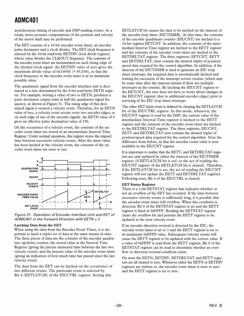
REV. B
ADMC401
–38–
asynchronous timing of encoder and DSP-reading events. As aresult, more accurate computations of the position and velocityof the motor shaft may be performed.
The EET consists of a 16-bit encoder event timer, an encoderpulse decimator and a clock divider. The EET clock frequency isselected by the 16-bit read/write EETDIV clock divide register,whose value divides the CLKOUT frequency. The contents ofthe encoder event timer are incremented on each rising edge ofthe divided clock signal. An EETDIV value of zero gives themaximum divide value of 0x10000 (= 65,536), so that theclock frequency to the encoder event timer is at its minimumpossible value.
The quadrature signal from the encoder interface unit is deci-mated at a rate determined by the 8-bit read/write EETN regis-ter. For example, writing a value of two to EETN, produces apulse decimator output train at half the quadrature signal fre-quency, as shown in Figure 31. The rising edge of this deci-mated signal is termed a velocity event. Therefore, for an EETNvalue of two, a velocity event occurs every two encoder edges, oron each edge of one of the encoder signals. An EETN value of 0gives an effective pulse decimation value of 256.
On the occurrence of a velocity event, the contents of the en-coder event timer are stored in an intermediate Interval TimeRegister. Under normal operation, this register stores the elapsedtime between successive velocity events. After the timer valuehas been latched at the velocity event, the contents of the en-coder event timer are reset to one.
ENCODER EVENTTIMER VALUE
EET LATCHEVENT
VELOCITYEVENTS
QUADRATURESIGNAL
EIUCNT
B
A
EETT
EETDELTAT
Figure 31. Operation of Encoder Interface Unit and EET ofADMC401 in the Forward Direction with EETN = 2
Latching Data from the EETWhen using the data from the Encoder Event Timer, it is im-portant to latch a triplet set of data at the same instant in time.The three pieces of data are the contents of the encoder quadra-ture up/down counter, the stored value in the Interval TimeRegister (giving the precise measured time between the last twovelocity events) and the present value of the encoder event timer(giving an indication of how much time has passed since the lastvelocity event).
The data from the EET can be latched on the occurrence oftwo different events. The particular event is selected byBit 4 (EETLATCH) of the EIUCTRL register. Setting this
EETLATCH bit causes the data to be latched on the timeout ofthe encoder loop timer (EIUTIMER). At that time, the contentsof the encoder quadrature counter (EIUCNT) are latched to a16-bit register EETCNT. In addition, the contents of the inter-mediate Interval Time register are latched to the EETT registerand the contents of the encoder event timer are latched to theEETDELTAT register. The three registers, EETCNT, EETTand EETDELTAT, then contain the desired triplet of position/speed data required for the control algorithm. In addition, if thetimeout of the EIUTIMER is used to generate an EIU looptimer interrupt, the required data is automatically latched andwaiting for execution of the interrupt service routine (which maybe some time after the timeout instant if there are multipleinterrupts in the system). By latching the EIUCNT register tothe EETCNT, the user does not have to worry about changes inthe EIUCNT register (due to additional encoder edges) prior toservicing of the EIU loop timer interrupt.
The other EET latch event is defined by clearing the EETLATCHbit of the EIUCTRL register. In this mode, whenever, theEIUCNT register is read by the DSP, the current value of theintermediate Interval Time register is latched to the EETTregister and the contents of the encoder event timer are latchedto the EETDELTAT register. The three registers, EIUCNT,EETT and EETDELTAT now contain the desired triplet ofposition/speed data required for the control algorithm. Note thedifference from before, in that the encoder count value is nowavailable in the EIUCNT register.
It is important to realize that the EETT, and EETDELTAT regis-ters are only updated by either the timeout of the EIUTIMERregister (if EETLATCH bit is set) or the act of reading theEIUCNT register (if the EETLATCH bit is cleared). Therefore,if the EETLATCH bit is set, the act of reading the EIUCNTregister will not update the EETT and EETDELTAT registers.Following reset, Bit 4 of the EIUCTRL is cleared.
EET Status RegisterThere is a 1-bit EETSTAT register that indicates whether ornot an overflow of the EET has occurred. If the time betweensuccessive velocity events is sufficiently long, it is possible thatthe encoder event timer will overflow. When this condition isdetected, Bit 0 of the EETSTAT register is set and the EETTregister is fixed at 0xFFFF. Reading the EETSTAT registerclears the overflow bit and permits the EETT register to beupdated at the next velocity event.
If an encoder direction reversal is detected by the EIU, theencoder event timer is set to 1 and the EETT register is set toits maximum 0xFFFF value. Subsequent velocity events willcause the EETT register to be updated with the correct value. Ifa value of 0xFFFF is read from the EETT register, Bit 0 of theEETSTAT register can be read to determine whether an over-flow or direction reversal condition exists.
On reset the EETN, EETDIV, EETDELTAT and EETT regis-ters are all cleared to zero. Whenever either the EETN or EETDIVregisters are written to, the encoder event timer is reset to zeroand the EETT register is set to zero.
ADMC401
–39–REV. B
EIU/EET RegistersThe structure and functionality of the EIU and EET registersare illustrated at the end of the data sheet. The characteristics ofthe EIU block at 26 MHz are given in Table VI.
PROGRAMMABLE DIGITAL INPUT/OUTPUTOVERVIEWThe ADMC401 has 12 programmable digital input/output pinscalled PIO0 to PIO11. Each pin may be individually configuredas either an input or an output. An associated data register maybe used to read data from pins configured as inputs and writedata to pins configured as outputs. In addition, each I/O linemay be configured as an interrupt source. Both edge (rising andfalling) and level (high and low) interrupts may be detected.Four of the PIO lines (PIO0 to PIO3) have dedicated vectoraddresses in the interrupt table. The remaining eight interrupts(PIO4 to PIO11) are multiplexed into a single additional inter-rupt vector location. The PIOFLAG register is used to deter-mine which line caused the interrupt. In addition, all PIO linesmay be alternatively configured as PWM trip sources. ThePIOPWM register has dedicated bits that may be used to enablethis function on each PIO line. In this mode, a low level on anypins configured as a PWM trip source shuts down the PWM ina manner identical to the PWMTRIP pin.
PIO CONFIGURATIONEach of the 12 programmable input/output lines may be config-ured as either an input or an output by programming the appro-priate bits of the PIODIR register. This 12-bit register has onebit associated with each I/O line; Bit 0 corresponds to PIO0, etc.Clearing a bit in the PIODIR register will configure the corre-sponding pin as an input line. Conversely, setting a bit config-ures the pin as an output pin. On reset, all bits of the PIODIRregister are cleared so that all 12 PIO pins are configured as inputs.In addition, all PIO lines have internal pull-down resistors in theADMC401 so that unconnected lines are seen as low level inputs.
PIO DATA READING/WRITINGAssociated with the PIO system is a data register, PIODATA,that also has a bit associated with each I/O line. Data written tothe PIODATA register will appear on those pins configured asoutputs. Reading the PIODATA register will read the data fromthose pins configured as inputs.
PIO INTERRUPT GENERATIONEach of the 12 PIO lines may be configured as an interruptsource. Four of the PIO lines, PIO0 to PIO3, have dedicatedinterrupt vector locations, whereas the remaining eight are mul-tiplexed into an additional interrupt vector. The PIOINTENregister is used to enable or disable the interrupt mode on the
PIO4 to PIO11 lines. The PICMASK register of the program-mable interrupt controller is used to enable interrupts on thefour dedicated PIO lines, PIO0 to PIO3, and to enable theusage of PIOINTEN for interrupts on the other PIOs.
Interrupts may be generated on either edge (rising or falling) orlevel (high or low) events by programming the appropriate bitsof both the PIOMODE and PIOLEVEL registers. Both registershave a dedicated bit for each of the twelve PIO lines. Setting theappropriate bit of the PIOMODE register configures the inter-rupt as level sensitive whereas clearing the bit configures theinterrupt for edge sensitive. In level-sensitive mode (PIOMODEbit is 1), setting the corresponding bit in the PIOLEVEL regis-ter configures the interrupt as active high, whereas clearing thebit configures it for active low. In edge-sensitive mode (PIOMODEbit is 0), setting the corresponding bit of the PIOLEVEL registerconfigures the interrupt for rising edge, whereas clearing the bitconfigures the interrupt for falling edge. On reset, all PIO inter-rupts are disabled.
The four dedicated PIO interrupts from PIO0 to PIO3 haveinterrupt vector addresses at program memory addresses 0x0048for PIO0, 0x004C for PIO1, 0x0050 for PIO2 and 0x0054 forPIO3. In the event of an interrupt on PIO4 to PIO11, the corre-sponding bit of the PIOFLAG register is set and the generalPIO interrupt is activated. This interrupt has a dedicated vectoraddress at location 0x003C. In the interrupt service routine forthis interrupt, the user must poll the PIOFLAG register to de-termine which of the PIO4 to PIO11 lines, that have interruptsenabled, caused the interrupt. Of course, if only one of the PIO4 toPIO11 lines has interrupts enabled, no polling is necessary.
PIO lines that are configured as outputs may also be used togenerate interrupts. If, for example, one of the PIO lines is con-figured simultaneously as an output and as an interrupt source,writing the appropriate data sequence to that line will trigger aninterrupt.
PIO AS PWMTRIP SOURCESBy setting the appropriate bits of the PIOPWM register, each ofthe twelve PIO lines can be configured as a PWM shutdownsource. In this mode, a low level on the PIO pin will cause aPWM shutdown command that will disable all six PWM out-puts on AH to CL. Since the disabling of the PWM is indepen-dent of the DSP clock, so that the PWM stage can be fullyprotected even in the event of a loss of clock signal to the DSP.In addition, a PWMTRIP interrupt will be generated when thePWM is shutdown. However, it is also possible to generate thenormal PIO interrupts on the occurrence of a falling-edge onthe PIO line. The advantage of this highly flexible structure forPWM shutdown is that multiple fault signals could be applied tothe ADMC401 at different PIO lines. The occurrence of a falling-
Table VI. Fundamental Characteristics of Encoder Interface Unit of ADMC401 (At 26 MHz)
Parameter Test Conditions Min Typ Max Unit
fENC Encoder Input (EIA, EIB) Rate 4.33 MHzfQUAD Quadrature Rate 17.3 MHz
Encoder Loop Timer Timeout Rate 38.5 ns0.645 sec
TMINENC Minimum Encoder Pulsewidth EIUFILTER = 0x00 116 nsEIUFILTER = 0x3F 7.39 µs
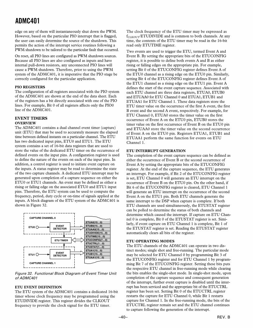
REV. B
ADMC401
–40–
edge on any of them will instantaneously shut down the PWM.However, based on the particular PIO interrupt that is flagged,the user can easily determine the source of the shutdown. Thispermits the action of the interrupt service routines following aPWM shutdown to be tailored to the particular fault that occurred.
On reset, all PIO lines are configured as PWM shutdown sources.Because all PIO lines are also configured as inputs and haveinternal pull-down resistors, any unconnected PIO lines willcause a PWM shutdown. Therefore, prior to using the PWMsystem of the ADMC401, it is imperative that the PIO stage becorrectly configured for the particular application.
PIO REGISTERSThe configuration of all registers associated with the PIO systemof the ADMC401 are shown at the end of the data sheet. Eachof the registers has a bit directly associated with one of the PIOlines. For example, Bit 0 of all registers affects only the PIO0line of the ADMC401.
EVENT TIMERSOVERVIEWThe ADMC401 contains a dual channel event timer (capture)unit (ETU) that may be used to accurately measure the elapsedtime between defined instants on a particular channel. The ETUhas two dedicated input pins, ETU0 and ETU1. The ETUsystem contains a set of 16-bit data registers that are used tostore the value of the dedicated ETU timer on the occurrence ofdefined events on the input pins. A configuration register is usedto define the nature of the events on each of the input pins. Inaddition, a control register is used to initiate event capture onthe inputs. A status register may be read to determine the stateof the two capture channels. A dedicated ETU interrupt may begenerated upon completion of a capture sequence on either theETU0 or ETU1 channels. An event may be defined as either arising or falling edge on the associated ETU0 and ETU1 inputpins. Therefore, the ETU system can be used to compute thefrequency, period, duty cycle or on-time of signals applied at theinputs. A block diagram of the ETU system of the ADMC401 isshown in Figure 32.
ETUA0(15…0)ETUB0(15…0)ETUAA0(15…0)ETUDIVIDE(15…0)ETUTIME(15…0)ETUCONFIG(7…0)ETUCTRL(1…0)ETUSTAT(1…0)ETUA1(15…0)ETUB1(15…0)ETUAA1(15…0)
CAPTURE CHANNEL 0
ETU TIMER
EVENTDETECTOR
EVENTDETECTOR
CAPTURE CHANNEL 1
ETU0
ETU1
Figure 32. Functional Block Diagram of Event Timer Unitof ADMC401
ETU EVENT DEFINITIONThe ETU system of the ADMC401 contains a dedicated 16-bittimer whose clock frequency may be programmed using theETUDIVIDE register. This register divides the CLKOUTfrequency to provide the clock signal for the ETU timer.
The clock frequency of the ETU timer may be expressed asfCLKOUT/ETUDIVIDE and is common to both channels. At anytime, the contents of the ETU timer may be read in the 16-bitread only ETUTIME register.
Two events are used to trigger the ETU, termed Event A andEvent B. By setting the appropriate bits of the ETUCONFIGregister, it is possible to define both events A and B as eitherrising or falling edges on the appropriate pin. For example,setting Bit 0 of the ETUCONFIG register defines Event A ofthe ETU0 channel as a rising edge on the ETU0 pin. Similarly,setting Bit 4 of the ETUCONFIG register defines Event A ofthe ETU1 channel as a rising edge on the ETU1 pin. Event Adefines the start of the event capture sequence. Associated witheach ETU channel are three data registers, ETUA0, ETUB0and ETUAA0 for ETU Channel 0 and ETUA1, ETUB1 andETUAA1 for ETU Channel 1. These data registers store theETU timer value on the occurrence of the first A event, the firstB event and the second A event, respectively. For example, forETU Channel 0, ETUA0 stores the timer value on the firstoccurrence of Event A on the ETU0 pin, ETUB0 stores thetimer value on the first occurrence of Event B on the ETU0 pinand ETUAA0 store the timer value on the second occurrenceof Event A on the ETU0 pin. Registers ETUA1, ETUB1 andETUAA1 perform the same function for events on ETUChannel 1.
ETU INTERRUPT GENERATIONThe completion of the event capture sequence can be defined aseither the occurrence of Event B or the second occurrence ofEvent A by setting the appropriate bits of the ETUCONFIGregister. At the end of the capture sequence, the ETU generatesan interrupt. For example, if Bit 2 of the ETUCONFIG registeris set, ETU Channel 0 will generate an ETU interrupt on theoccurrence of Event B on the ETU0 pin. On the other hand, ifBit 6 of the ETUCONFIG register is cleared, ETU Channel 1will generate an ETU interrupt on the occurrence of the secondEvent A on the ETU1 pin. Both ETU channels generate thesame interrupt to the DSP when capture is complete. If bothETU channels are used simultaneously, the ETUSTAT registercan be polled to determine the status of both channels anddetermine which caused the interrupt. If capture on ETU Chan-nel 0 is complete, Bit 0 of the ETUSTAT register is set. Simi-larly, if event capture on ETU Channel 1 is complete, Bit 1 ofthe ETUSTAT register is set. Reading the ETUSTAT registerautomatically clears all bits of the register.
ETU OPERATING MODESThe ETU channels of the ADMC401 can operate in two dis-tinct modes; single shot and free-running. The particular modemay be selected for ETU Channel 0 by programming Bit 3 ofthe ETUCONFIG register and for ETU Channel 1 by program-ming Bit 7 of the ETUCONFIG register. Setting these bits putsthe respective ETU channel in free-running mode while clearingthe bits enables the single-shot mode. In single-shot mode, uponcompletion of the capture sequence and consequent generationof the interrupt, further event capture is disabled until the inter-rupt has been serviced and the appropriate bit of the ETUCTRLregister has been set. Setting Bit 0 of the ETUCTRL registerrestarts the capture for ETU Channel 0, while Bit 1 restartscapture for Channel 1. In the free-running mode, the bits of theETUCTRL register remain set and the ETU channel continuesto capture following the generation of the interrupt.
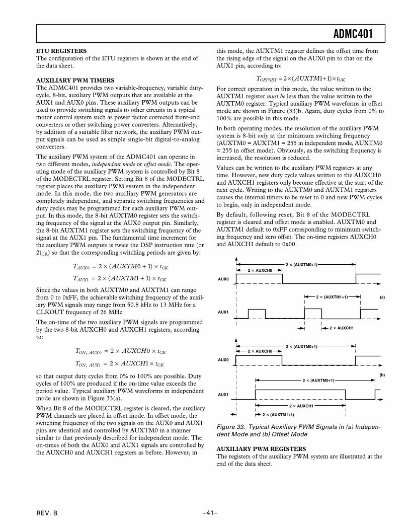
ADMC401
–41–REV. B
ETU REGISTERSThe configuration of the ETU registers is shown at the end ofthe data sheet.
AUXILIARY PWM TIMERSThe ADMC401 provides two variable-frequency, variable duty-cycle, 8-bit, auxiliary PWM outputs that are available at theAUX1 and AUX0 pins. These auxiliary PWM outputs can beused to provide switching signals to other circuits in a typicalmotor control system such as power factor corrected front-endconverters or other switching power converters. Alternatively,by addition of a suitable filter network, the auxiliary PWM out-put signals can be used as simple single-bit digital-to-analogconverters.
The auxiliary PWM system of the ADMC401 can operate intwo different modes, independent mode or offset mode. The oper-ating mode of the auxiliary PWM system is controlled by Bit 8of the MODECTRL register. Setting Bit 8 of the MODECTRLregister places the auxiliary PWM system in the independentmode. In this mode, the two auxiliary PWM generators arecompletely independent, and separate switching frequencies andduty cycles may be programmed for each auxiliary PWM out-put. In this mode, the 8-bit AUXTM0 register sets the switch-ing frequency of the signal at the AUX0 output pin. Similarly,the 8-bit AUXTM1 register sets the switching frequency of thesignal at the AUX1 pin. The fundamental time increment forthe auxiliary PWM outputs is twice the DSP instruction rate (or2tCK) so that the corresponding switching periods are given by:
T AUXTM t
T AUXTM t
AUX CK
AUX CK
0
1
2 0 1
2 1 1
= × + ×
= × + ×
( )
( )
Since the values in both AUXTM0 and AUXTM1 can rangefrom 0 to 0xFF, the achievable switching frequency of the auxil-iary PWM signals may range from 50.8 kHz to 13 MHz for aCLKOUT frequency of 26 MHz.
The on-time of the two auxiliary PWM signals are programmedby the two 8-bit AUXCH0 and AUXCH1 registers, accordingto:
T AUXCH t
T AUXCH t
ON AUX CK
ON AUX CK
,
,
0
1
2 0
2 1
= × ×
= × ×
so that output duty cycles from 0% to 100% are possible. Dutycycles of 100% are produced if the on-time value exceeds theperiod value. Typical auxiliary PWM waveforms in independentmode are shown in Figure 33(a).
When Bit 8 of the MODECTRL register is cleared, the auxiliaryPWM channels are placed in offset mode. In offset mode, theswitching frequency of the two signals on the AUX0 and AUX1pins are identical and controlled by AUXTM0 in a mannersimilar to that previously described for independent mode. Theon-times of both the AUX0 and AUX1 signals are controlled bythe AUXCH0 and AUXCH1 registers as before. However, in
this mode, the AUXTM1 register defines the offset time fromthe rising edge of the signal on the AUX0 pin to that on theAUX1 pin, according to:
T AUXTM tOFFSET CK= × + ×2 1 1( )
For correct operation in this mode, the value written to theAUXTM1 register must be less than the value written to theAUXTM0 register. Typical auxiliary PWM waveforms in offsetmode are shown in Figure (33)b. Again, duty cycles from 0% to100% are possible in this mode.
In both operating modes, the resolution of the auxiliary PWMsystem is 8-bit only at the minimum switching frequency(AUXTM0 = AUXTM1 = 255 in independent mode, AUXTM0= 255 in offset mode). Obviously, as the switching frequency isincreased, the resolution is reduced.
Values can be written to the auxiliary PWM registers at anytime. However, new duty cycle values written to the AUXCH0and AUXCH1 registers only become effective at the start of thenext cycle. Writing to the AUXTM0 and AUXTM1 registerscauses the internal timers to be reset to 0 and new PWM cyclesto begin, only in independent mode.
By default, following reset, Bit 8 of the MODECTRLregister is cleared and offset mode is enabled. AUXTM0 andAUXTM1 default to 0xFF corresponding to minimum switch-ing frequency and zero offset. The on-time registers AUXCH0and AUXCH1 default to 0x00.
2 AUXCH0
2 AUXCH0
(a)
(b)
AUX0
AUX1
AUX0
AUX1
2 (AUXTM0+1)
2 (AUXTM1+1)
2 AUXCH1
2 (AUXTM0+1)
2 (AUXTM1+1)
2 (AUXTM0+1)
2 AUXCH1
Figure 33. Typical Auxiliary PWM Signals in (a) Indepen-dent Mode and (b) Offset Mode
AUXILIARY PWM REGISTERSThe registers of the auxiliary PWM system are illustrated at theend of the data sheet.
REV. B
ADMC401
–42–
WATCHDOG TIMEROVERVIEWThe watchdog timer is used as a protection mechanism againstunintentional software events causing the DSP to become stuckin infinite loops. It can be used to cause a complete DSP andperipheral reset in the event of such a software error. The watch-dog timer consists of a 16-bit timer that is clocked at the CLKINrate, tCKI.
The watchdog timer is disabled after a master reset (RESET =LO). This also resets the WDFLAG bit in the SYSSTAT regis-ter. The watchdog timer is enabled by writing a TIMEOUT valueto the WDTIMER register. Once the watchdog timer has beeninitialized, the timer is decremented at the CLKIN rate. Inorder to prevent a watchdog timer trip, it is necessary to writeagain to the WDTIMER register. For all writes to the WDTIMERregister (subsequent to the initial write), it is unimportant whichvalue is written. The act of writing to the WDTIMER registerautomatically reloads the initial TIMEOUT value. If the watch-dog timer is not rewritten to after an interval:
TWDT = WDTIMER × tCKI
the watchdog timer will decrement to zero and a watchdog tripwill be generated. In this case, a complete reset of the DSP coreand motor control peripherals (except the watchdog timeritself) is initiated and Bit 1 of the SYSSTAT register (WDFLAG)is set. Following a reset, the DSP core can determine if the resetwas caused by a watchdog trip (and if so take appropriate ac-tion) or if it was due to the normal reset sequence. The watchdogtimer remains disabled while the WDFLAG is set to preventcontinuous watchdog trips. The watchdog timer can be restartedand the WDFLAG reset by writing a nonzero TIMEOUT valueto the WDTIMER register. The WDFLAG will be reset, butthe watchdog timer will remain disabled if 0x0000 is written tothe WDTIMER register.
The watchdog timer is only reset by a low input on the RESETpin. The watchdog circuit is not reset by a software controlledPeripheral Reset.
PROGRAMMABLE INTERRUPT CONTROLLEROVERVIEWThe ADMC401 uses the IRQ2 pin of the DSP core to generatea peripheral interrupt. There are multiple sources of peripheralinterrupts, e.g., the ADC block, PIO block, EIU block, ETUblock and PWM block. A Programmable Interrupt Controller(PIC) is used to avoid a software latency in determining thesource of the interrupt. With the occurrence of an interruptfrom the peripheral blocks, the PIC block generates an addressthat points to the corresponding vector address in the DSP vectortable. The PIC consists of an output register, PICVECTOR,that contains a pointer to an entry in the DSP vector table.During normal operation, an interrupt service routine (ISR)located at vector address 0x0004 (or the IRQ2/peripheral inter-rupt) jumps to the address pointed to by the PICVECTORregister. The necessary code to perform this jump from address0x0004 is automatically placed there by the internal ROM codewhen MMAP = BMODE = 1.
The vector addresses between 0x00 and 0x2C are reservedfor the DSP core interrupts. The vector table addresses fromPM(0x30) to PM(0x58) are reserved for use by peripheral inter-rupt service routines. Each vector address occupies four addresses
of PM. The priority of the peripheral interrupts is fixed in hard-ware. The ISR at address PM(0x30) has the highest prioritywhereas the ISR at address PM(0x58) has the lowest.
In the case of multiple simultaneous interrupts, the PIC willload the PICVECTOR register with the interrupt that has thehighest priority. Between reads of the PICVECTOR register(while the DSP is servicing other interrupts for example)PICVECTOR is updated with the highest priority of any periph-eral interrupts. This ensures that when the IRQ2 is reasserted,the highest priority interrupt that occurred since the last readingof the PICVECTOR register is now waiting to be serviced.
When PICVECTOR is read, if another interrupt is pending inthe PIC, then the IRQ2 line to the DSP remains LO and no edgewill be seen. In order to catch all interrupts, IRQ2 interruptsshould be configured as level sensitive in the ICNTL register.
The four least significant PIO pins are assigned unique vectoraddresses. An interrupt on any of the remaining eight lines(PIO4 to PIO11) will trigger a separate fifth PIO interrupt thathas its own vector address. The PIOFLAG register can be readto determine the exact source of this fifth interrupt. An 11-bitPICMASK register can be used to enable or disable any or all ofthe eleven peripheral interrupt sources. The program memoryaddress reserved for each of the interrupts is summarized inTable VII.
Table VII. Interrupt Vector Addresses
Function Vector Address
RESET Startup (or Power Up withPUCR = 1) 0x00 (Highest Priority)
Power-Down (Nonmaskable) 0x2CADC End-of-Conversion Interrupt 0x30PWMSYNC Interrupt 0x34EIU Loop Timer Timeout Interrupt 0x38PIO4 to PIO11 Interrupt 0x3CEIU Counter Error Interrupt 0x40ETU Interrupt 0x44PIO0 Interrupt 0x48PIO1 Interrupt 0x4CPIO2 Interrupt 0x50PIO3 Interrupt 0x54PWM Trip Interrupt 0x58SPORT0 Transmit 0x10SPORT0 Receive 0x14Software Interrupt 1 0x18Software Interrupt 0 0x1CSPORT1 Transmit (or IRQ1) 0x20SPORT1 Receive (or IRQ0) 0x24Interval Timer Interrupt 0x28 (Lowest Priority)
Interrupt MaskingInterrupt masking (or disabling) is controlled by the IMASKregister of the DSP core and the PICMASK register. Theseregisters contain individual bits that must be set to enable thevarious interrupt sources. It is important to remember that ifany peripheral interrupt is to be enabled both the IRQ2interrupt enable bit (Bit 9) of the IMASK register and theappropriate bit of the PICMASK register must be set. Theconfiguration of both the IMASK and PICMASK registers ofthe ADMC401 is shown at the end of the data sheet.
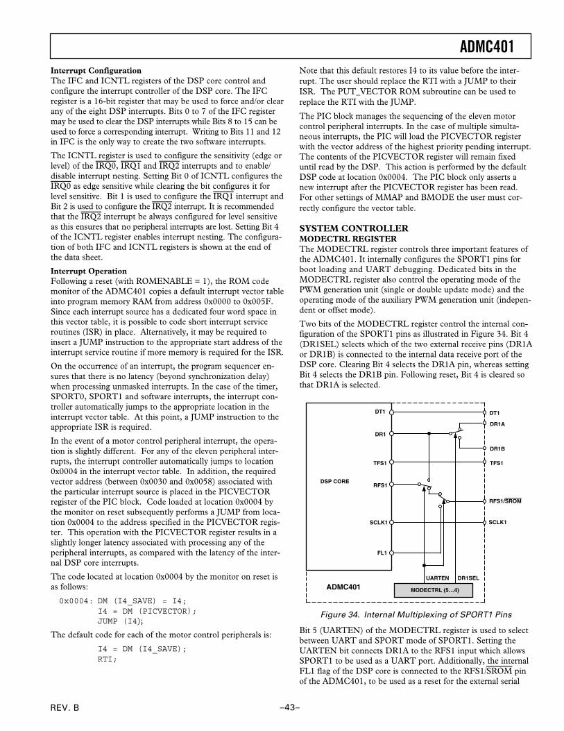
ADMC401
–43–REV. B
Interrupt ConfigurationThe IFC and ICNTL registers of the DSP core control andconfigure the interrupt controller of the DSP core. The IFCregister is a 16-bit register that may be used to force and/or clearany of the eight DSP interrupts. Bits 0 to 7 of the IFC registermay be used to clear the DSP interrupts while Bits 8 to 15 can beused to force a corresponding interrupt. Writing to Bits 11 and 12in IFC is the only way to create the two software interrupts.
The ICNTL register is used to configure the sensitivity (edge orlevel) of the IRQ0, IRQ1 and IRQ2 interrupts and to enable/disable interrupt nesting. Setting Bit 0 of ICNTL configures theIRQ0 as edge sensitive while clearing the bit configures it forlevel sensitive. Bit 1 is used to configure the IRQ1 interrupt andBit 2 is used to configure the IRQ2 interrupt. It is recommendedthat the IRQ2 interrupt be always configured for level sensitiveas this ensures that no peripheral interrupts are lost. Setting Bit 4of the ICNTL register enables interrupt nesting. The configura-tion of both IFC and ICNTL registers is shown at the end ofthe data sheet.
Interrupt OperationFollowing a reset (with ROMENABLE = 1), the ROM codemonitor of the ADMC401 copies a default interrupt vector tableinto program memory RAM from address 0x0000 to 0x005F.Since each interrupt source has a dedicated four word space inthis vector table, it is possible to code short interrupt serviceroutines (ISR) in place. Alternatively, it may be required toinsert a JUMP instruction to the appropriate start address of theinterrupt service routine if more memory is required for the ISR.
On the occurrence of an interrupt, the program sequencer en-sures that there is no latency (beyond synchronization delay)when processing unmasked interrupts. In the case of the timer,SPORT0, SPORT1 and software interrupts, the interrupt con-troller automatically jumps to the appropriate location in theinterrupt vector table. At this point, a JUMP instruction to theappropriate ISR is required.
In the event of a motor control peripheral interrupt, the opera-tion is slightly different. For any of the eleven peripheral inter-rupts, the interrupt controller automatically jumps to location0x0004 in the interrupt vector table. In addition, the requiredvector address (between 0x0030 and 0x0058) associated withthe particular interrupt source is placed in the PICVECTORregister of the PIC block. Code loaded at location 0x0004 bythe monitor on reset subsequently performs a JUMP from loca-tion 0x0004 to the address specified in the PICVECTOR regis-ter. This operation with the PICVECTOR register results in aslightly longer latency associated with processing any of theperipheral interrupts, as compared with the latency of the inter-nal DSP core interrupts.
The code located at location 0x0004 by the monitor on reset isas follows:
0x0004: DM (I4_SAVE) = I4;I4 = DM (PICVECTOR);JUMP (I4);
The default code for each of the motor control peripherals is:
I4 = DM (I4_SAVE);RTI;
Note that this default restores I4 to its value before the inter-rupt. The user should replace the RTI with a JUMP to theirISR. The PUT_VECTOR ROM subroutine can be used toreplace the RTI with the JUMP.
The PIC block manages the sequencing of the eleven motorcontrol peripheral interrupts. In the case of multiple simulta-neous interrupts, the PIC will load the PICVECTOR registerwith the vector address of the highest priority pending interrupt.The contents of the PICVECTOR register will remain fixeduntil read by the DSP. This action is performed by the defaultDSP code at location 0x0004. The PIC block only asserts anew interrupt after the PICVECTOR register has been read.For other settings of MMAP and BMODE the user must cor-rectly configure the vector table.
SYSTEM CONTROLLERMODECTRL REGISTERThe MODECTRL register controls three important features ofthe ADMC401. It internally configures the SPORT1 pins forboot loading and UART debugging. Dedicated bits in theMODECTRL register also control the operating mode of thePWM generation unit (single or double update mode) and theoperating mode of the auxiliary PWM generation unit (indepen-dent or offset mode).
Two bits of the MODECTRL register control the internal con-figuration of the SPORT1 pins as illustrated in Figure 34. Bit 4(DR1SEL) selects which of the two external receive pins (DR1Aor DR1B) is connected to the internal data receive port of theDSP core. Clearing Bit 4 selects the DR1A pin, whereas settingBit 4 selects the DR1B pin. Following reset, Bit 4 is cleared sothat DR1A is selected.
DSP CORE
DR1A
DR1B
TFS1
RFS1/SROM
MODECTRL (5…4)
UARTEN DR1SEL
DT1
DR1
TFS1
RFS1
FL1
ADMC401
DT1
SCLK1 SCLK1
Figure 34. Internal Multiplexing of SPORT1 Pins
Bit 5 (UARTEN) of the MODECTRL register is used to selectbetween UART and SPORT mode of SPORT1. Setting theUARTEN bit connects DR1A to the RFS1 input which allowsSPORT1 to be used as a UART port. Additionally, the internalFL1 flag of the DSP core is connected to the RFS1/SROM pinof the ADMC401, to be used as a reset for the external serial

REV. B
ADMC401
–44–
ROM or E2PROM. Clearing the UARTEN bit selects SPORTmode, so that SPORT1 is configured in a manner identical tothe standard serial ports of the ADSP-21xx family. Followingreset, the UARTEN bit is cleared so that SPORT mode is selected.
Bit 6 of the MODECTRL register is used to select betweensingle update and double update operating modes of the PWMgeneration unit. Clearing this bit selects single update mode,while setting it selects double update mode. Following reset,this bit is cleared so that single update mode is the defaultconfiguration.
Bit 8 of the MODECTRL register is used to select betweenindependent and offset operating modes of the auxiliary PWMunit. Clearing this bit selects offset mode, while setting it selectsindependent mode. Following reset, this bit is cleared so thatoffset mode is the default configuration.
SYSSTAT REGISTERThe SYSSTAT register provides various status information ofthe ADMC401, such as the state of the PWMTRIP pin, thestate of the watchdog flag, the state of the PWMPOL pin andphase of the PWM
Bit 0 indicates the state of the PWMTRIP pin such that the bitis set if PWMTRIP is HI and cleared if the pin is LO. Similarly,Bit 2 indicates the state of the PWMPOL pin such that the bit isset if PWMPOL is HI (active high PWM selected) and cleared ifthe pin is LO (active low PWM selected).
Bit 1 is used to indicate if a watchdog timer timeout has oc-curred. This bit is set following a watchdog timeout and can beread on reset to determine if the reset is a normal power-onreset or due to a watchdog trip.
Bit 3 of the SYSSTAT register is used to identify the half cycleof operation of the PWM generation unit. During the first halfcycle, when the internal PWM timer is decrementing, this bit iscleared. During the second half cycle, this bit is set while thetimer is incrementing.
SYSTEM CONTROL REGISTERSThe configuration of the MODECTRL and SYSSTAT registeris shown at the end of the data sheet.
PERIPHERAL AND DSP CORE REGISTERSThe address, name, type, used bits and reset value of all of theperipheral registers of the ADMC401 are given in Table VIII.Similarly, the DSP core registers of the ADMC401 are tabu-lated in Table IX.
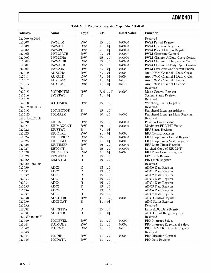
ADMC401
–45–REV. B
Table VIII. Peripheral Register Map of the ADMC401
Address Name Type Bits Reset Value Function
0x2000–0x2007 Reserved0x2008 PWMTM R/W [15 . . . 0] 0x0000 PWM Period Register0x2009 PWMDT R/W [9 . . . 0] 0x0000 PWM Deadtime Register0x200A PWMPD R/W [9 . . . 0] 0x0000 PWM Pulse Deletion Register0x200B PWMGATE R/W [9 . . . 0] 0x000 PWM Chopping Control0x200C PWMCHA R/W [15 . . . 0] 0x0000 PWM Channel A Duty Cycle Control0x200D PWMCHB R/W [15 . . . 0] 0x0000 PWM Channel B Duty Cycle Control0x200E PWMCHC R/W [15 . . . 0] 0x0000 PWM Channel C Duty Cycle Control0x200F PWMSEG R/W [8 . . . 0] 0x000 PWM Crossover and Output Enable0x2010 AUXCH0 R/W [7 . . . 0] 0x00 Aux. PWM Channel 0 Duty Cycle0x2011 AUXCH1 R/W [7 . . . 0] 0x00 Aux. PWM Channel 1 Duty Cycle0x2012 AUXTM0 R/W [7 . . . 0] 0xFF Aux. PWM Channel 0 Period0x2013 AUXTM1 R/W [7 . . . 0] 0xFF Aux. PWM Channel 1 Period0x2014 Reserved0x2015 MODECTRL R/W [8, 6 . . . 4] 0x000 Mode Control Register0x2016 SYSSTAT R [3 . . . 0] System Status Register0x2017 Reserved0x2018 WDTIMER R/W [15 . . . 0] Watchdog Timer Register0x2019–0x201B Reserved0x201C PICVECTOR R [15 . . . 0] Peripheral Interrupt Address0x201D PICMASK R/W [10 . . . 0] 0x000 Peripheral Interrupt Mask Register0x201E–0x201F Reserved0x2020 EIUCNT R/W [15 . . . 0] 0x0000 Position Count Value0x2021 EIUMAXCNT R/W [15 . . . 0] 0x0000 Maximum EIUCNT Value0x2022 EIUSTAT R [7 . . . 0] EIU Status Register0x2023 EIUCTRL R/W [8 . . . 0] 0x000 EIU Control Register0x2024 EIUPERIOD R/W [15 . . . 0] 0x0000 EIU Loop Timer Period Register0x2025 EIUSCALE R/W [7 . . . 0] 0x00 EIU Loop Timer Scale Register0x2026 EIUTIMER R/W [15 . . . 0] 0x0000 EIU Loop Timer Register0x2027 EETCNT R [15 . . . 0] 0x0000 Latched Copy of EIUCNT0x2028 EIUFILTER R/W [5 . . . 0] 0x00 EIU Filter Control Register0x2029 EIZLATCH R [15 . . . 0] EIZ Latch Register0x202A EISLATCH R [15 . . . 0] EIS Latch Register0x202B–0x202F Reserved0x2030 ADC0 R [15 . . . 0] ADC0 Data Register0x2031 ADC1 R [15 . . . 0] ADC1 Data Register0x2032 ADC2 R [15 . . . 0] ADC2 Data Register0x2033 ADC3 R [15 . . . 0] ADC3 Data Register0x2034 ADC4 R [15 . . . 0] ADC4 Data Register0x2035 ADC5 R [15 . . . 0] ADC5 Data Register0x2036 ADC6 R [15 . . . 0] ADC6 Data Register0x2037 ADC7 R [15 . . . 0] ADC7 Data Register0x2038 ADCCTRL R/W [4 . . . 3,0] 0x00 ADC Control Register0x2039 ADCSTAT R [4 . . . 0] ADC Status Register0x203A Reserved0x203B ADCXTRA R [15 . . . 0] Extra ADC Data Register0x203C ADCOTR R [7 . . . 0] ADC Out of Range Register0x203D–0x203F Reserved0x2040 PIOLEVEL R/W [11 . . . 0] 0x000 PIO Interrupt Select0x2041 PIOMODE R/W [11 . . . 0] 0x000 PIO Interrupt Edge/Level Select0x2042 PIOPWM R/W [11 . . . 0] 0xFFF PIO PWMTRIP Enable Register0x2043 Reserved0x2044 PIODIR R/W [11 . . . 0] 0x000 PIO Direction Control0x2045 PIODATA R/W [11 . . . 0] PIO Data Register
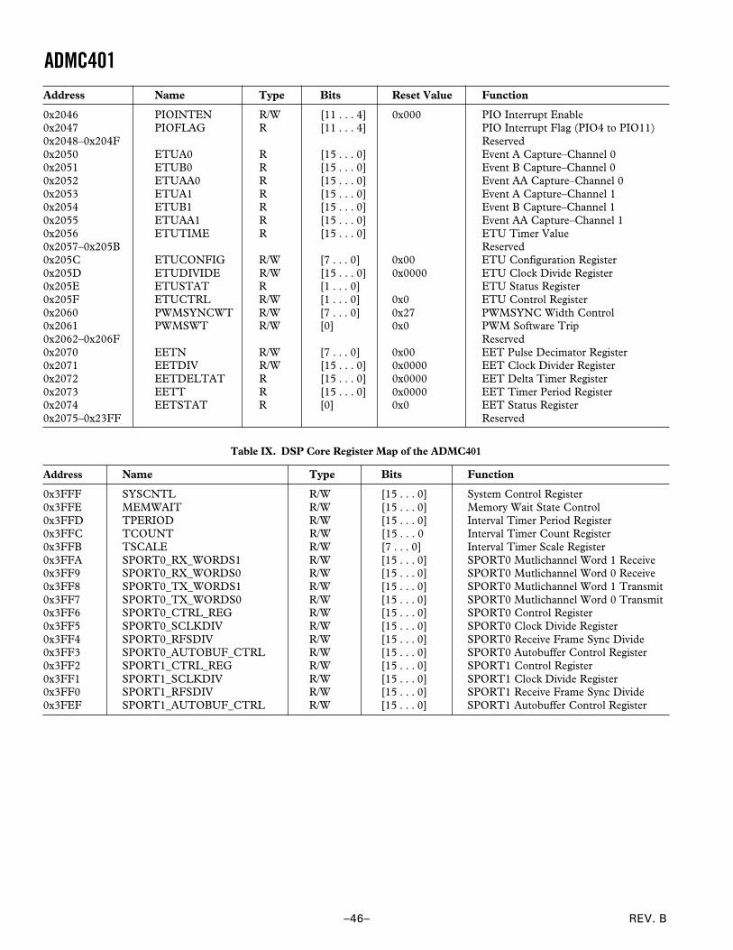
REV. B
ADMC401
–46–
Address Name Type Bits Reset Value Function
0x2046 PIOINTEN R/W [11 . . . 4] 0x000 PIO Interrupt Enable0x2047 PIOFLAG R [11 . . . 4] PIO Interrupt Flag (PIO4 to PIO11)0x2048–0x204F Reserved0x2050 ETUA0 R [15 . . . 0] Event A Capture–Channel 00x2051 ETUB0 R [15 . . . 0] Event B Capture–Channel 00x2052 ETUAA0 R [15 . . . 0] Event AA Capture–Channel 00x2053 ETUA1 R [15 . . . 0] Event A Capture–Channel 10x2054 ETUB1 R [15 . . . 0] Event B Capture–Channel 10x2055 ETUAA1 R [15 . . . 0] Event AA Capture–Channel 10x2056 ETUTIME R [15 . . . 0] ETU Timer Value0x2057–0x205B Reserved0x205C ETUCONFIG R/W [7 . . . 0] 0x00 ETU Configuration Register0x205D ETUDIVIDE R/W [15 . . . 0] 0x0000 ETU Clock Divide Register0x205E ETUSTAT R [1 . . . 0] ETU Status Register0x205F ETUCTRL R/W [1 . . . 0] 0x0 ETU Control Register0x2060 PWMSYNCWT R/W [7 . . . 0] 0x27 PWMSYNC Width Control0x2061 PWMSWT R/W [0] 0x0 PWM Software Trip0x2062–0x206F Reserved0x2070 EETN R/W [7 . . . 0] 0x00 EET Pulse Decimator Register0x2071 EETDIV R/W [15 . . . 0] 0x0000 EET Clock Divider Register0x2072 EETDELTAT R [15 . . . 0] 0x0000 EET Delta Timer Register0x2073 EETT R [15 . . . 0] 0x0000 EET Timer Period Register0x2074 EETSTAT R [0] 0x0 EET Status Register0x2075–0x23FF Reserved
Table IX. DSP Core Register Map of the ADMC401
Address Name Type Bits Function
0x3FFF SYSCNTL R/W [15 . . . 0] System Control Register0x3FFE MEMWAIT R/W [15 . . . 0] Memory Wait State Control0x3FFD TPERIOD R/W [15 . . . 0] Interval Timer Period Register0x3FFC TCOUNT R/W [15 . . . 0 Interval Timer Count Register0x3FFB TSCALE R/W [7 . . . 0] Interval Timer Scale Register0x3FFA SPORT0_RX_WORDS1 R/W [15 . . . 0] SPORT0 Mutlichannel Word 1 Receive0x3FF9 SPORT0_RX_WORDS0 R/W [15 . . . 0] SPORT0 Mutlichannel Word 0 Receive0x3FF8 SPORT0_TX_WORDS1 R/W [15 . . . 0] SPORT0 Mutlichannel Word 1 Transmit0x3FF7 SPORT0_TX_WORDS0 R/W [15 . . . 0] SPORT0 Mutlichannel Word 0 Transmit0x3FF6 SPORT0_CTRL_REG R/W [15 . . . 0] SPORT0 Control Register0x3FF5 SPORT0_SCLKDIV R/W [15 . . . 0] SPORT0 Clock Divide Register0x3FF4 SPORT0_RFSDIV R/W [15 . . . 0] SPORT0 Receive Frame Sync Divide0x3FF3 SPORT0_AUTOBUF_CTRL R/W [15 . . . 0] SPORT0 Autobuffer Control Register0x3FF2 SPORT1_CTRL_REG R/W [15 . . . 0] SPORT1 Control Register0x3FF1 SPORT1_SCLKDIV R/W [15 . . . 0] SPORT1 Clock Divide Register0x3FF0 SPORT1_RFSDIV R/W [15 . . . 0] SPORT1 Receive Frame Sync Divide0x3FEF SPORT1_AUTOBUF_CTRL R/W [15 . . . 0] SPORT1 Autobuffer Control Register
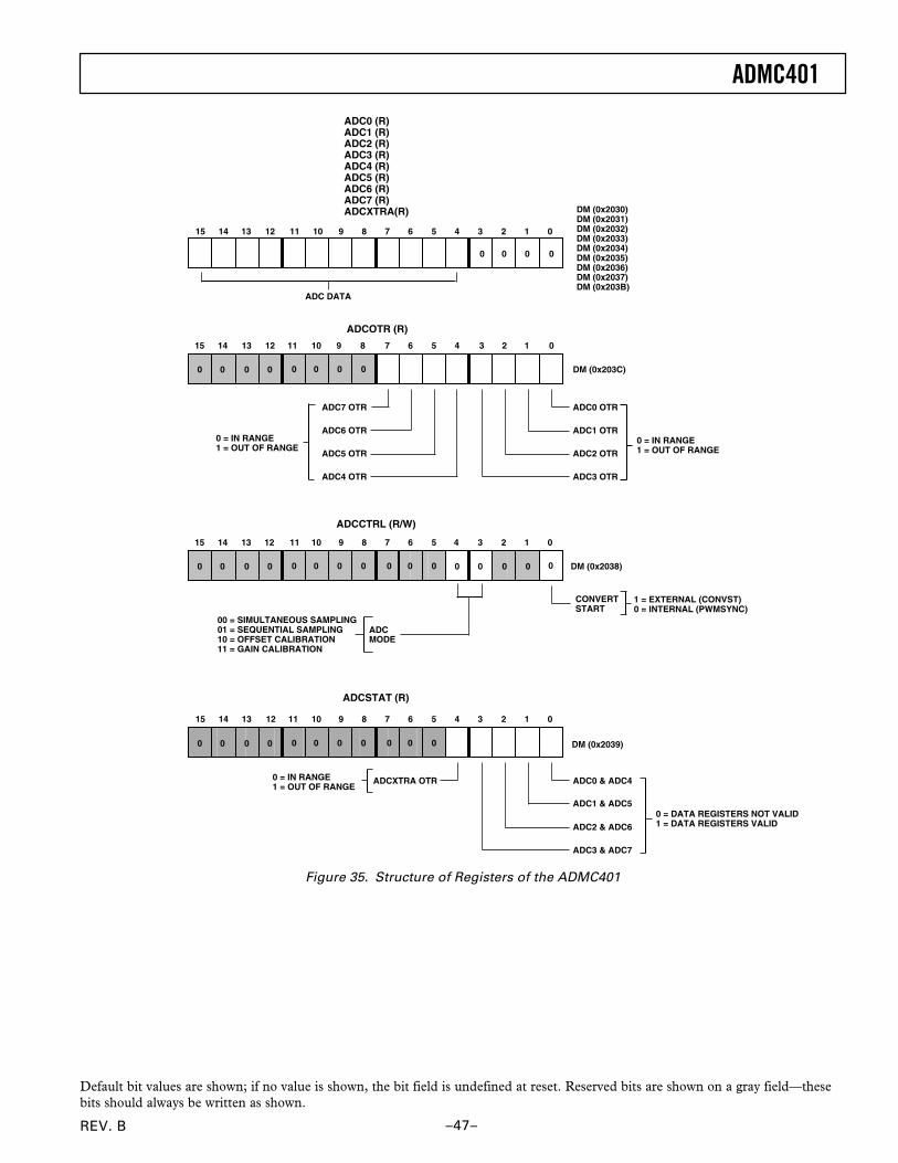
ADMC401
–47–REV. B
00000000
00 DM (0x2038)
CONVERTSTART
ADCCTRL (R/W)
1 = EXTERNAL (CONVST)0 = INTERNAL (PWMSYNC)
ADCOTR (R)
DM (0x203C)
0 = IN RANGE1 = OUT OF RANGE
ADC0 (R)ADC1 (R)ADC2 (R)ADC3 (R)ADC4 (R)ADC5 (R)ADC6 (R)ADC7 (R)ADCXTRA(R) DM (0x2030)
DM (0x2031)DM (0x2032)DM (0x2033)DM (0x2034)DM (0x2035)DM (0x2036)DM (0x2037)DM (0x203B)
DM (0x2039)
ADCSTAT (R)
15 14 13 12 11 10 9 8 7 6 5 4 3 2 1 0
15 14 13 12 11 10 9 8 7 6 5 4 3 2 1 0
15 14 13 12 11 10 9 8 7 6 5 4 3 2 1 0
15 14 13 12 11 10 9 8 7 6 5 4 3 2 1 0
0000
ADC DATA
ADC0 OTR
ADC1 OTR
ADC3 OTR
ADC2 OTR
ADC7 OTR
ADC6 OTR
ADC4 OTR
ADC5 OTR
0 = IN RANGE1 = OUT OF RANGE
0
00 = SIMULTANEOUS SAMPLING01 = SEQUENTIAL SAMPLING10 = OFFSET CALIBRATION11 = GAIN CALIBRATION
ADCMODE
ADC0 & ADC4
ADC1 & ADC5
ADC3 & ADC7
ADC2 & ADC6
0 = DATA REGISTERS NOT VALID1 = DATA REGISTERS VALID
ADCXTRA OTR0 = IN RANGE1 = OUT OF RANGE
00000000 000 00
00000000 000
Figure 35. Structure of Registers of the ADMC401
Default bit values are shown; if no value is shown, the bit field is undefined at reset. Reserved bits are shown on a gray field—thesebits should always be written as shown.
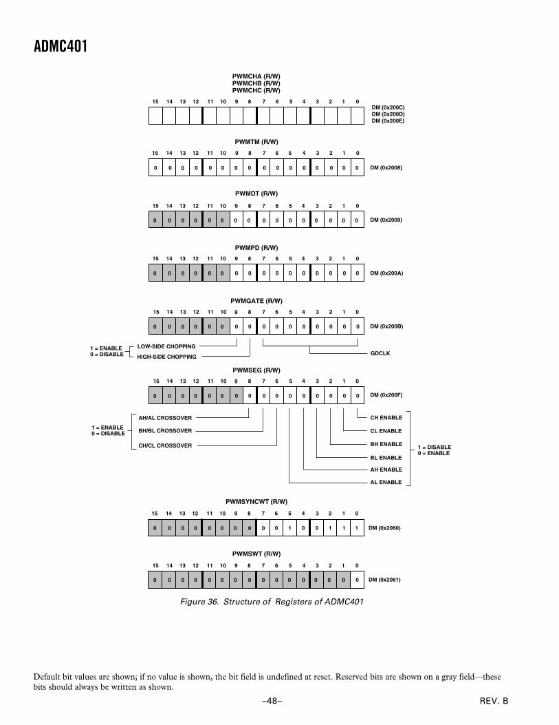
REV. B
ADMC401
–48–
15 14 13 12 11 10 9 8 7 6 5 4 3 2 1 0
0 0 0 0 0 0 00 0 0
PWMTM (R/W)
DM (0x2008)
PWMCHA (R/W)PWMCHB (R/W)PWMCHC (R/W)
DM (0x200C)DM (0x200D)DM (0x200E)
15 14 13 12 11 10 9 8 7 6 5 4 3 2 1 0
1 = DISABLE0 = ENABLE
CH ENABLE
CL ENABLE
BH ENABLE
BL ENABLE
AH ENABLE
AL ENABLE
AH/AL CROSSOVER
BH/BL CROSSOVER
CH/CL CROSSOVER
DM (0x200F)
PWMSEG (R/W)
15 14 13 12 11 10 9 8 7 6 5 4 3 2 1 0
0 1 0 0 1 1 10
PWMSYNCWT (R/W)
DM (0x2060)
15 14 13 12 11 10 9 8 7 6 5 4 3 2 1 0
0
PWMSWT (R/W)
DM (0x2061)
15 14 13 12 11 10 9 8 7 6 5 4 3 2 1 0
0 0 0 0 0 0 00 0 0
PWMDT (R/W)
DM (0x2009)
PWMGATE (R/W)
DM (0x200B)
GDCLK1 = ENABLE0 = DISABLE
LOW-SIDE CHOPPING
HIGH-SIDE CHOPPING
1 = ENABLE0 = DISABLE
15 14 13 12 11 10 9 8 7 6 5 4 3 2 1 0
0 0 0 0 0 0 00 0 0
PWMPD (R/W)
DM (0x200A)
0 0 00 0 0
0 0 00 0 0
0 0 00 0 0
0 0 00 0 0 0 0
00 0 00 0 0 0 0 0 0 00 0 0
15 14 13 12 11 10 9 8 7 6 5 4 3 2 1 0
0 0 0 0 0 0 00 0 00 0 00 0 0
15 14 13 12 11 10 9 8 7 6 5 4 3 2 1 0
0 0 0 0 0 0 00 0 00 0 00 0 0
0
0
Figure 36. Structure of Registers of ADMC401
Default bit values are shown; if no value is shown, the bit field is undefined at reset. Reserved bits are shown on a gray field—thesebits should always be written as shown.
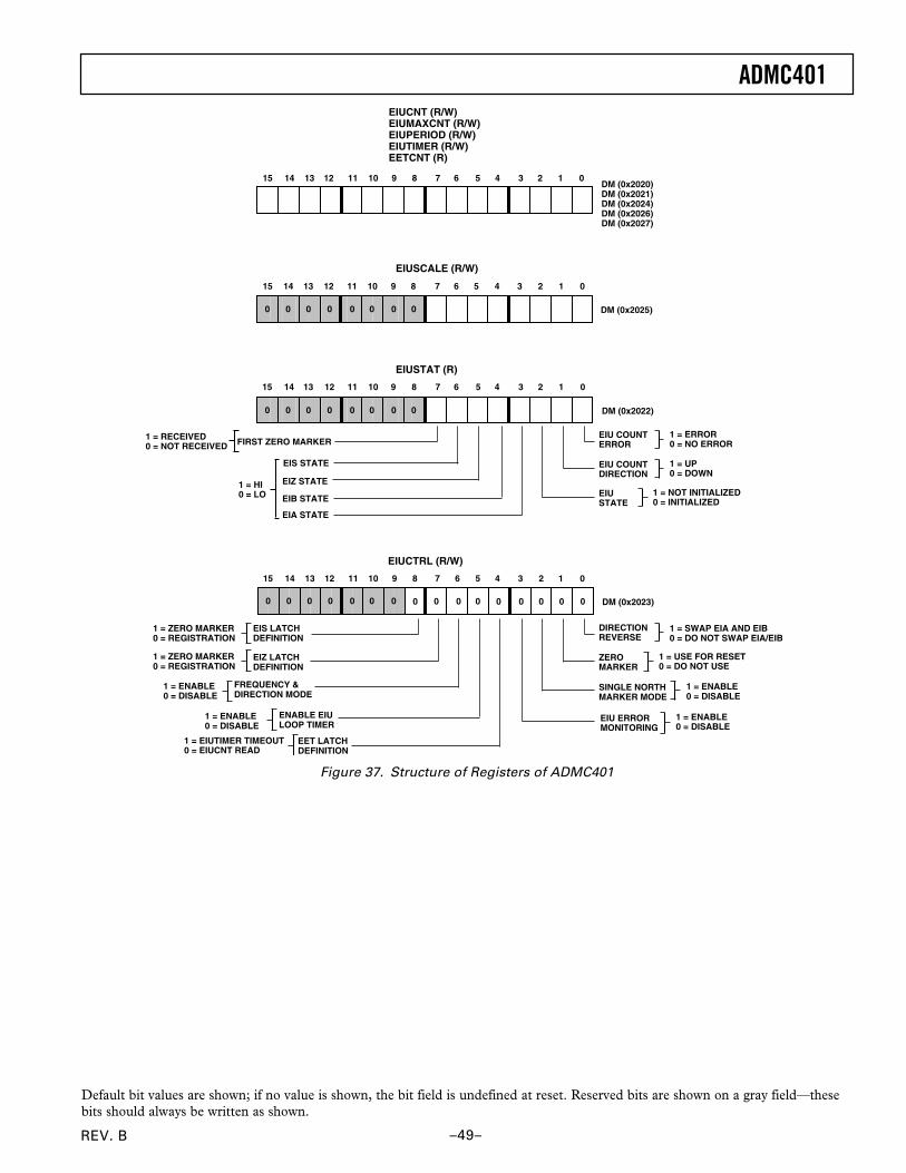
ADMC401
–49–REV. B
Default bit values are shown; if no value is shown, the bit field is undefined at reset. Reserved bits are shown on a gray field—thesebits should always be written as shown.
00 0000 DM (0x2023)
EIUCTRL (R/W)
FIRST ZERO MARKER1 = RECEIVED0 = NOT RECEIVED
EIU COUNTERROR
1 = ERROR0 = NO ERROR
EIU COUNTDIRECTION
1 = UP0 = DOWN
EIUSTATE
1 = NOT INITIALIZED0 = INITIALIZED
DM (0x2022)
EIUSTAT (R)
15 14 13 12 11 10 9 8 7 6 5 4 3 2 1 0
15 14 13 12 11 10 9 8 7 6 5 4 3 2 1 0
15 14 13 12 11 10 9 8 7 6 5 4 3 2 1 0
EIUSCALE (R/W)
15 14 13 12 11 10 9 8 7 6 5 4 3 2 1 0
EIUCNT (R/W)EIUMAXCNT (R/W)EIUPERIOD (R/W)EIUTIMER (R/W)EETCNT (R)
DM (0x2020)DM (0x2021)DM (0x2024)DM (0x2026)DM (0x2027)
DM (0x2025)
EIS STATE
EIZ STATE
EIB STATE
1 = HI0 = LO
DIRECTIONREVERSE
1 = SWAP EIA AND EIB0 = DO NOT SWAP EIA/EIB
ZEROMARKER
1 = USE FOR RESET0 = DO NOT USE
SINGLE NORTHMARKER MODE
1 = ENABLE0 = DISABLE
1 = ZERO MARKER0 = REGISTRATION
1 = ENABLE0 = DISABLE
FREQUENCY &DIRECTION MODE
EIA STATE
000
1 = ENABLE0 = DISABLE
EIU ERRORMONITORING
EIS LATCHDEFINITION
EIZ LATCHDEFINITION
ENABLE EIULOOP TIMER
EET LATCHDEFINITION
1 = EIUTIMER TIMEOUT0 = EIUCNT READ
1 = ENABLE0 = DISABLE
1 = ZERO MARKER0 = REGISTRATION
0 0 0 0 0 0 0 0
0 0 0 0 0 0 0 0
0 0 0 0 0 0 0
Figure 37. Structure of Registers of ADMC401
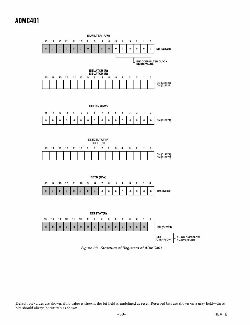
REV. B
ADMC401
–50–
15 14 13 12 11 10 9 8 7 6 5 4 3 2 1 0
0 = NO OVERFLOW1 = OVERFLOW
EETSTAT(R)
DM (0x2074)
EETOVERFLOW
000000 DM (0x2028)
EIUFILTER (R/W)
DM (0x2070)
EETN (R/W)
DM (0x2029)
EIZLATCH (R)EISLATCH (R)
000000000000000
EETDIV (R/W)
15 14 13 12 11 10 9 8 7 6 5 4 3 2 1 0
15 14 13 12 11 10 9 8 7 6 5 4 3 2 1 0
15 14 13 12 11 10 9 8 7 6 5 4 3 2 1 0
15 14 13 12 11 10 9 8 7 6 5 4 3 2 1 0
ENCODER FILTER CLOCKDIVIDE VALUE
DM (0x202A)
0000000000000000
00000000
DM (0x2071)
0000000000
00000000
EETDELTAT (R)EETT (R)
15 14 13 12 11 10 9 8 7 6 5 4 3 2 1 0
DM (0x2072)DM (0x2073)
Figure 38. Structure of Registers of ADMC401
Default bit values are shown; if no value is shown, the bit field is undefined at reset. Reserved bits are shown on a gray field—thesebits should always be written as shown.
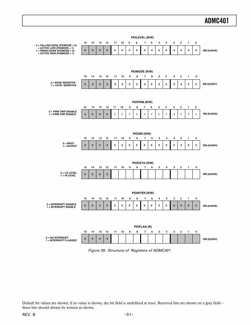
ADMC401
–51–REV. B
PIOLEVEL (R/W)
DM (0x2040)
0 = FALLING EDGE (PIOMODE = 0) = ACTIVE LOW (PIOMODE = 1)1 = RISING EDGE (PIOMODE = 0) = ACTIVE HIGH (PIOMODE = 1)
15 14 13 12 11 10 9 8 7 6 5 4 3 2 1 0
000000000000
DM (0x2041)0 = EDGE SENSITIVE1 = LEVEL SENSITIVE
PIOMODE (R/W)
15 14 13 12 11 10 9 8 7 6 5 4 3 2 1 0
000000000000
DM (0x2042)0 = PWM TRIP DISABLE1 = PWM TRIP ENABLE
PIOPWM (R/W)
15 14 13 12 11 10 9 8 7 6 5 4 3 2 1 0
1111 1111 1111
DM (0x2044)0 = INPUT1 = OUTPUT
PIODIR (R/W)
000000000000
15 14 13 12 11 10 9 8 7 6 5 4 3 2 1 0
0000
PIOFLAG (R)
DM (0x2047)0 = NO INTERRUPT1 = INTERRUPT FLAGGED
DM (0x2046)
PIOINTEN (R/W)
0 = INTERRUPT DISABLE1 = INTERRUPT ENABLE
DM (0x2045)0 = LO LEVEL1 = HI LEVEL
PIODATA (R/W)
0000
0000
0000
15 14 13 12 11 10 9 8 7 6 5 4 3 2 1 0
0000
00000000
15 14 13 12 11 10 9 8 7 6 5 4 3 2 1 0
0000
15 14 13 12 11 10 9 8 7 6 5 4 3 2 1 0
0000
0000
Figure 39. Structure of Registers of ADMC401
Default bit values are shown; if no value is shown, the bit field is undefined at reset. Reserved bits are shown on a gray field—these bits should always be written as shown.
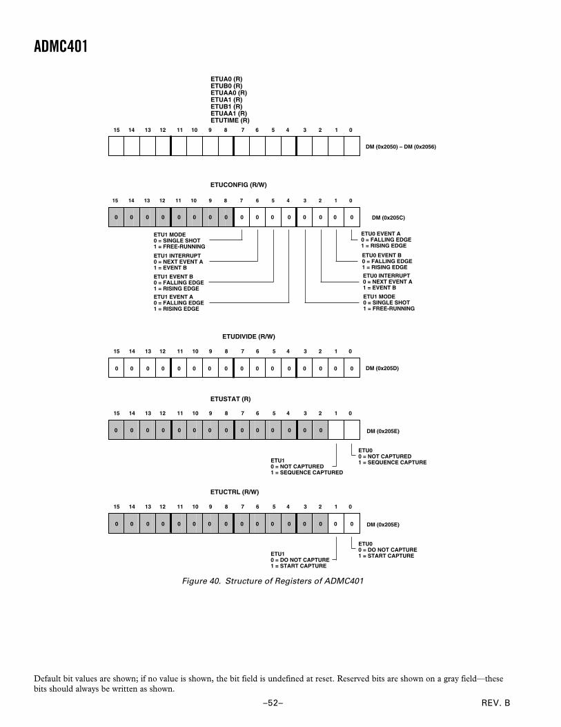
REV. B
ADMC401
–52–
ETUCTRL (R/W)
DM (0x205E)
ETU00 = DO NOT CAPTURE1 = START CAPTURE
DM (0x205D)
ETUDIVIDE (R/W)
DM (0x2050) – DM (0x2056)
15 14 13 12 11 10 9 8 7 6 5 4 3 2 1 0
15 14 13 12 11 10 9 8 7 6 5 4 3 2 1 0
DM (0x205C)
15 14 13 12 11 10 9 8 7 6 5 4 3 2 1 0
ETUCONFIG (R/W)
ETU1 MODE0 = SINGLE SHOT1 = FREE-RUNNING
ETU1 INTERRUPT0 = NEXT EVENT A1 = EVENT B
ETU1 EVENT B0 = FALLING EDGE1 = RISING EDGE
ETU1 EVENT A0 = FALLING EDGE1 = RISING EDGE
ETU0 EVENT A0 = FALLING EDGE1 = RISING EDGE
ETU0 EVENT B0 = FALLING EDGE1 = RISING EDGE
ETU0 INTERRUPT0 = NEXT EVENT A1 = EVENT B
ETU1 MODE0 = SINGLE SHOT1 = FREE-RUNNING
ETUA0 (R)ETUB0 (R)ETUAA0 (R)ETUA1 (R)ETUB1 (R)ETUAA1 (R)ETUTIME (R)
ETU10 = DO NOT CAPTURE1 = START CAPTURE
ETUSTAT (R)
DM (0x205E)
ETU00 = NOT CAPTURED1 = SEQUENCE CAPTUREETU1
0 = NOT CAPTURED1 = SEQUENCE CAPTURED
0000000000000000
0000000000000000
15 14 13 12 11 10 9 8 7 6 5 4 3 2 1 0
00000000000000
15 14 13 12 11 10 9 8 7 6 5 4 3 2 1 0
0000000000000000
Figure 40. Structure of Registers of ADMC401
Default bit values are shown; if no value is shown, the bit field is undefined at reset. Reserved bits are shown on a gray field—thesebits should always be written as shown.
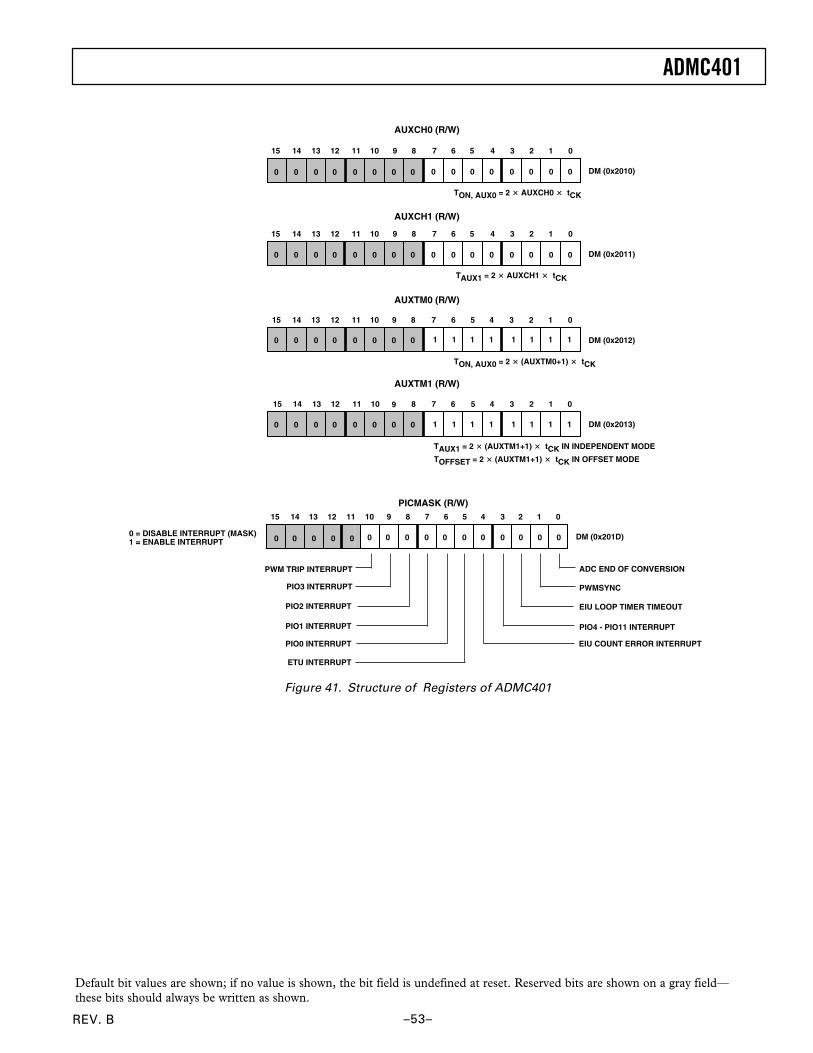
ADMC401
–53–REV. B
15 14 13 12 11 10 9 8 7 6 5 4 3 2 1 0
0 0 0 0 0 0 00 DM (0x2011)
ADC END OF CONVERSION
PWMSYNC
EIU LOOP TIMER TIMEOUT
PIO4 - PIO11 INTERRUPT
EIU COUNT ERROR INTERRUPT
DM (0x201D)
PICMASK (R/W)15 14 13 12 11 10 9 8 7 6 5 4 3 2 1 0
15 14 13 12 11 10 9 8 7 6 5 4 3 2 1 0
0 0 0 0 0 0 00
DM (0x2012)
15 14 13 12 11 10 9 8 7 6 5 4 3 2 1 0
DM (0x2013)
0 = DISABLE INTERRUPT (MASK)1 = ENABLE INTERRUPT
PWM TRIP INTERRUPT
PIO3 INTERRUPT
PIO2 INTERRUPT
PIO1 INTERRUPT
PIO0 INTERRUPT
ETU INTERRUPT
11111111
0 00
15 14 13 12 11 10 9 8 7 6 5 4 3 2 1 0
0 0 0 0 0 0 00
AUXCH0 (R/W)
DM (0x2010)
11111111
TON, AUX0 = 2 AUXCH0 tCK
AUXTM0 (R/W)
AUXTM1 (R/W)
TAUX1 = 2 AUXCH1 tCK
TON, AUX0 = 2 (AUXTM0+1) tCK
TAUX1 = 2 (AUXTM1+1) tCK IN INDEPENDENT MODE
TOFFSET = 2 (AUXTM1+1) tCK IN OFFSET MODE
AUXCH1 (R/W)
0 0 0 000 00
0 0 0 000 00
0 0 0 000 00
0 0 0 000 00
00 00 0
Figure 41. Structure of Registers of ADMC401
Default bit values are shown; if no value is shown, the bit field is undefined at reset. Reserved bits are shown on a gray field—these bits should always be written as shown.
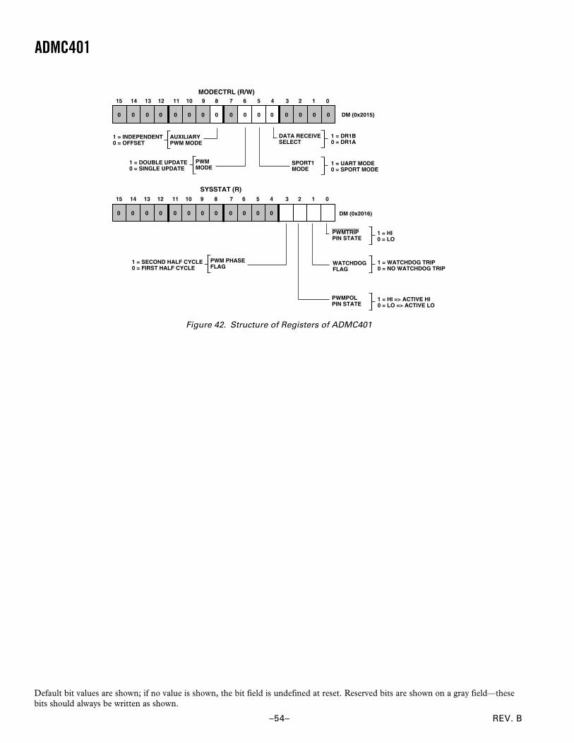
REV. B
ADMC401
–54–
MODECTRL (R/W)
DM (0x2015)
DATA RECEIVESELECT
1 = DR1B0 = DR1A
1 = UART MODE0 = SPORT MODE
SPORT1MODE
SYSSTAT (R)
DM (0x2016)
1 = HI0 = LO
1 = WATCHDOG TRIP0 = NO WATCHDOG TRIP
PWMTRIPPIN STATE
WATCHDOGFLAG
PWMPOLPIN STATE
15 14 13 12 11 10 9 8 7 6 5 4 3 2 1 0
15 14 13 12 11 10 9 8 7 6 5 4 3 2 1 0
000
PWM PHASEFLAG
1 = SECOND HALF CYCLE0 = FIRST HALF CYCLE
PWMMODE
1 = DOUBLE UPDATE0 = SINGLE UPDATE
0
AUXILIARYPWM MODE
1 = INDEPENDENT0 = OFFSET
1 = HI => ACTIVE HI0 = LO => ACTIVE LO
00000000 0000
0000 00000000
Figure 42. Structure of Registers of ADMC401
Default bit values are shown; if no value is shown, the bit field is undefined at reset. Reserved bits are shown on a gray field—thesebits should always be written as shown.
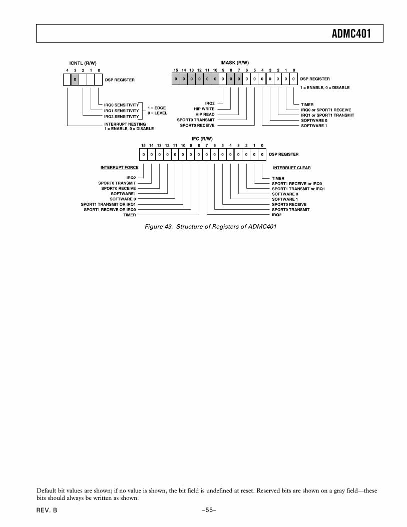
ADMC401
–55–REV. B
TIMERSPORT1 RECEIVE or IRQ0SPORT1 TRANSMIT or IRQ1SOFTWARE 0SOFTWARE 1SPORT0 RECEIVESPORT0 TRANSMITIRQ2
IRQ2SPORT0 TRANSMIT
SPORT0 RECEIVESOFTWARE1SOFTWARE 0
SPORT1 TRANSMIT OR IRQ1SPORT1 RECEIVE OR IRQ0
TIMER
INTERRUPT FORCE INTERRUPT CLEAR
IFC (R/W)9 8 7 6 5 4 3 2 1 0101112131415
0000000000000 0 0 0
IRQ0 SENSITIVITYIRQ1 SENSITIVITYIRQ2 SENSITIVITY
INTERRUPT NESTING1 = ENABLE, 0 = DISABLE
0
ICNTL (R/W)
1 = EDGE0 = LEVEL
4 3 2 1 0 101112131415 9 8 7 6 5 4 3 2 1 0
IRQ2HIP WRITEHIP READ
SPORT0 TRANSMITSPORT0 RECEIVE
IMASK (R/W)
DSP REGISTER
1 = ENABLE, 0 = DISABLE
0000000000000000
TIMERIRQ0 or SPORT1 RECEIVEIRQ1 or SPORT1 TRANSMITSOFTWARE 0SOFTWARE 1
DSP REGISTER
DSP REGISTER
Figure 43. Structure of Registers of ADMC401
Default bit values are shown; if no value is shown, the bit field is undefined at reset. Reserved bits are shown on a gray field—thesebits should always be written as shown.
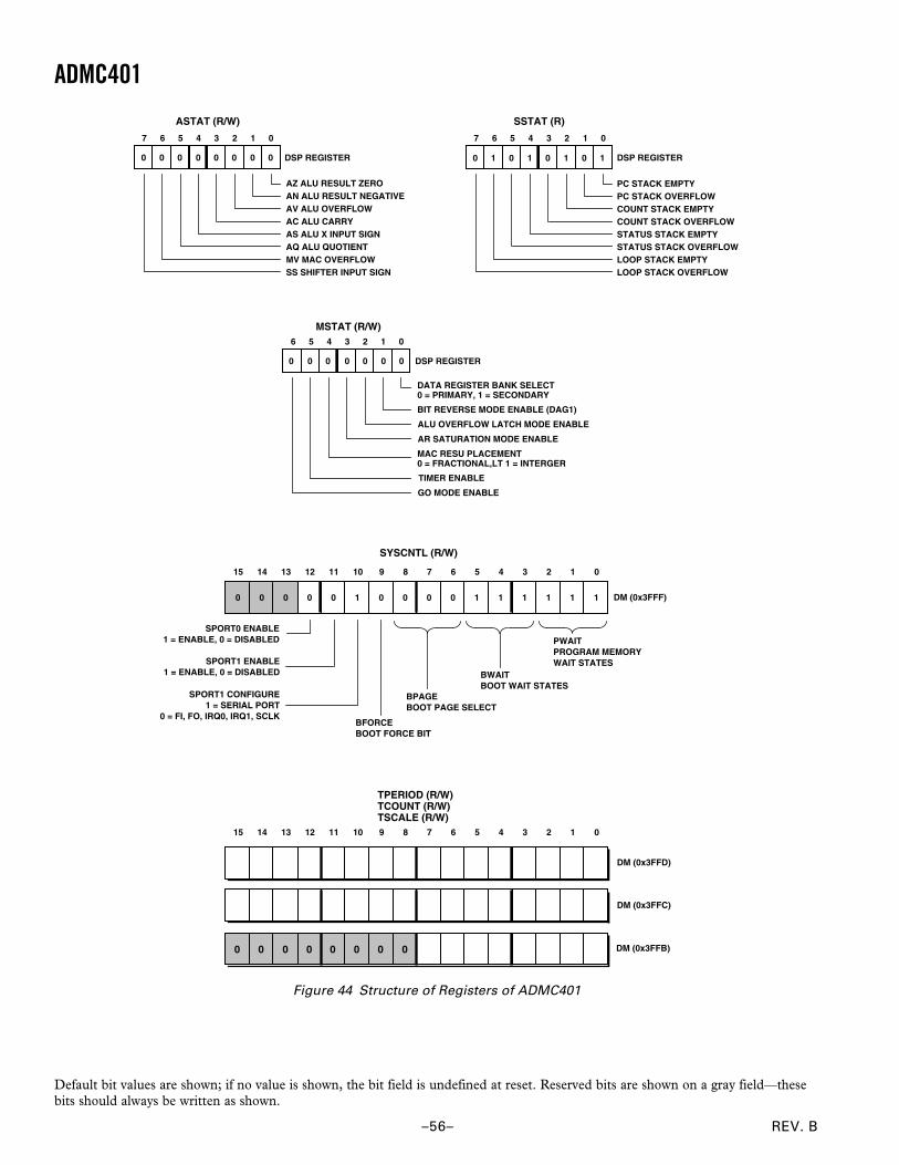
REV. B
ADMC401
–56–
DM (0x3FFC)
TPERIOD (R/W)TCOUNT (R/W)TSCALE (R/W)
DM (0x3FFD)
DM (0x3FFB)
15 14 13 12 11 10 9 8 7 6 5 4 3 2 1 0
0000000 0
SSTAT (R)
PC STACK EMPTYPC STACK OVERFLOWCOUNT STACK EMPTYCOUNT STACK OVERFLOWSTATUS STACK EMPTYSTATUS STACK OVERFLOWLOOP STACK EMPTYLOOP STACK OVERFLOW
7 6 5 4 3 2 1 0
10101010
MSTAT (R/W)6 5 4 3 2 1 0
0000000 DSP REGISTER
DATA REGISTER BANK SELECT0 = PRIMARY, 1 = SECONDARY
BIT REVERSE MODE ENABLE (DAG1)
ALU OVERFLOW LATCH MODE ENABLE
AR SATURATION MODE ENABLE
MAC RESU PLACEMENT0 = FRACTIONAL,LT 1 = INTERGER
TIMER ENABLE
GO MODE ENABLE
SYSCNTL (R/W)
PWAITPROGRAM MEMORYWAIT STATES
15 14 13 12 11 10 9 8 7 6 5 4 3 2 1 0
BPAGEBOOT PAGE SELECT
BWAITBOOT WAIT STATES
BFORCEBOOT FORCE BIT
SPORT0 ENABLE1 = ENABLE, 0 = DISABLED
10100000 11 111000 DM (0x3FFF)
SPORT1 ENABLE1 = ENABLE, 0 = DISABLED
SPORT1 CONFIGURE1 = SERIAL PORT
0 = FI, FO, IRQ0, IRQ1, SCLK
AZ ALU RESULT ZEROAN ALU RESULT NEGATIVEAV ALU OVERFLOWAC ALU CARRYAS ALU X INPUT SIGNAQ ALU QUOTIENTMV MAC OVERFLOWSS SHIFTER INPUT SIGN
7 6 5 4 3 2 1 0
ASTAT (R/W)
00000000 DSP REGISTER DSP REGISTER
Figure 44 Structure of Registers of ADMC401
Default bit values are shown; if no value is shown, the bit field is undefined at reset. Reserved bits are shown on a gray field—thesebits should always be written as shown.
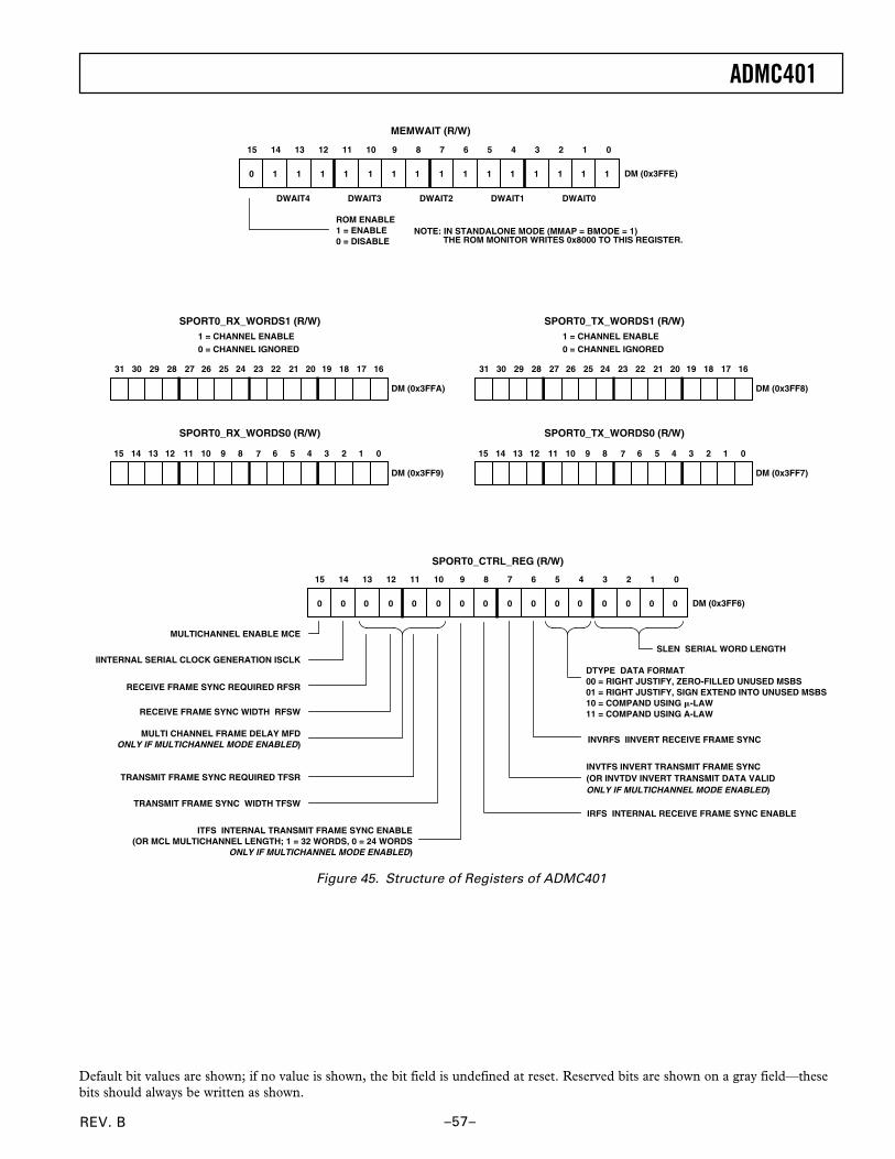
ADMC401
–57–REV. B
31 30 29 28 27 26 25 24 23 22 21 20 19 18 17 16
SPORT0_RX_WORDS1 (R/W)1 = CHANNEL ENABLE0 = CHANNEL IGNORED
DM (0x3FFA)
15 14 13 12 11 10 9 8 7 6 5 4 3 2 1 0
SPORT0_RX_WORDS0 (R/W)
DM (0x3FF9)
31 30 29 28 27 26 25 24 23 22 21 20 19 18 17 16
SPORT0_TX_WORDS1 (R/W)1 = CHANNEL ENABLE0 = CHANNEL IGNORED
DM (0x3FF8)
15 14 13 12 11 10 9 8 7 6 5 4 3 2 1 0
SPORT0_TX_WORDS0 (R/W)
DM (0x3FF7)
MEMWAIT (R/W)
DWAIT4 DWAIT0DWAIT1DWAIT2DWAIT3
ROM ENABLE1 = ENABLE0 = DISABLE
11111110 11 111111
15 14 13 12 11 10 9 8 7 6 5 4 3 2 1 0
NOTE: IN STANDALONE MODE (MMAP = BMODE = 1) THE ROM MONITOR WRITES 0x8000 TO THIS REGISTER.
DM (0x3FFE)
MULTICHANNEL ENABLE MCE
IINTERNAL SERIAL CLOCK GENERATION ISCLK
RECEIVE FRAME SYNC REQUIRED RFSR
RECEIVE FRAME SYNC WIDTH RFSW
MULTI CHANNEL FRAME DELAY MFDONLY IF MULTICHANNEL MODE ENABLED)
TRANSMIT FRAME SYNC REQUIRED TFSR
TRANSMIT FRAME SYNC WIDTH TFSW
SLEN SERIAL WORD LENGTH
DTYPE DATA FORMAT00 = RIGHT JUSTIFY, ZERO-FILLED UNUSED MSBS01 = RIGHT JUSTIFY, SIGN EXTEND INTO UNUSED MSBS10 = COMPAND USING -LAW11 = COMPAND USING A-LAW
ITFS INTERNAL TRANSMIT FRAME SYNC ENABLE(OR MCL MULTICHANNEL LENGTH; 1 = 32 WORDS, 0 = 24 WORDS
ONLY IF MULTICHANNEL MODE ENABLED)
INVRFS IINVERT RECEIVE FRAME SYNC
INVTFS INVERT TRANSMIT FRAME SYNC(OR INVTDV INVERT TRANSMIT DATA VALIDONLY IF MULTICHANNEL MODE ENABLED)
IRFS INTERNAL RECEIVE FRAME SYNC ENABLE
SPORT0_CTRL_REG (R/W)
00000000 00 000000
15 14 13 12 11 10 9 8 7 6 5 4 3 2 1 0
DM (0x3FF6)
Figure 45. Structure of Registers of ADMC401
Default bit values are shown; if no value is shown, the bit field is undefined at reset. Reserved bits are shown on a gray field—thesebits should always be written as shown.
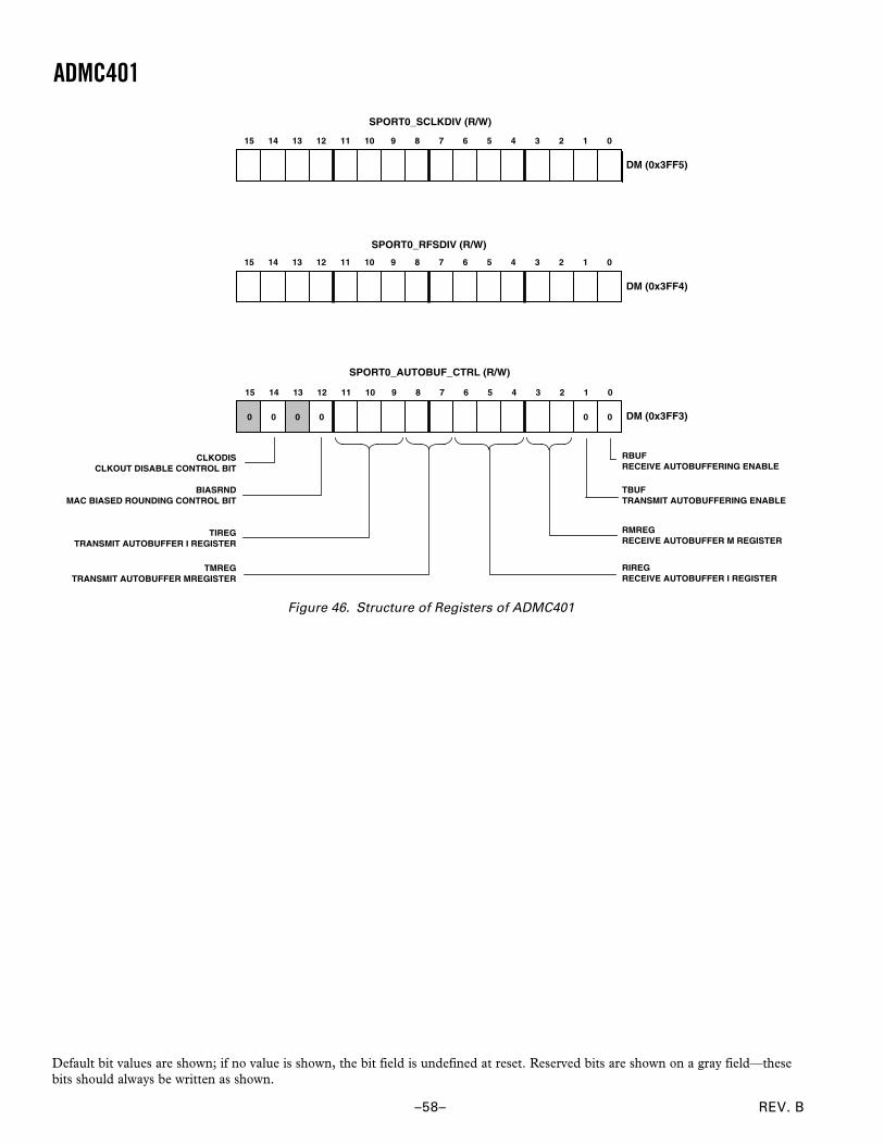
REV. B
ADMC401
–58–
SPORT0_AUTOBUF_CTRL (R/W)
15 14 13 12 11 10 9 8 7 6 5 4 3 2 1 0
0000 0 0
RBUFRECEIVE AUTOBUFFERING ENABLE
TBUFTRANSMIT AUTOBUFFERING ENABLE
RMREGRECEIVE AUTOBUFFER M REGISTER
RIREGRECEIVE AUTOBUFFER I REGISTER
CLKODISCLKOUT DISABLE CONTROL BIT
BIASRNDMAC BIASED ROUNDING CONTROL BIT
TIREGTRANSMIT AUTOBUFFER I REGISTER
TMREGTRANSMIT AUTOBUFFER MREGISTER
DM (0x3FF3)
SPORT0_SCLKDIV (R/W)
SPORT0_RFSDIV (R/W)
15 14 13 12 11 10 9 8 7 6 5 4 3 2 1 0
15 14 13 12 11 10 9 8 7 6 5 4 3 2 1 0
DM (0x3FF4)
DM (0x3FF5)
Figure 46. Structure of Registers of ADMC401
Default bit values are shown; if no value is shown, the bit field is undefined at reset. Reserved bits are shown on a gray field—thesebits should always be written as shown.
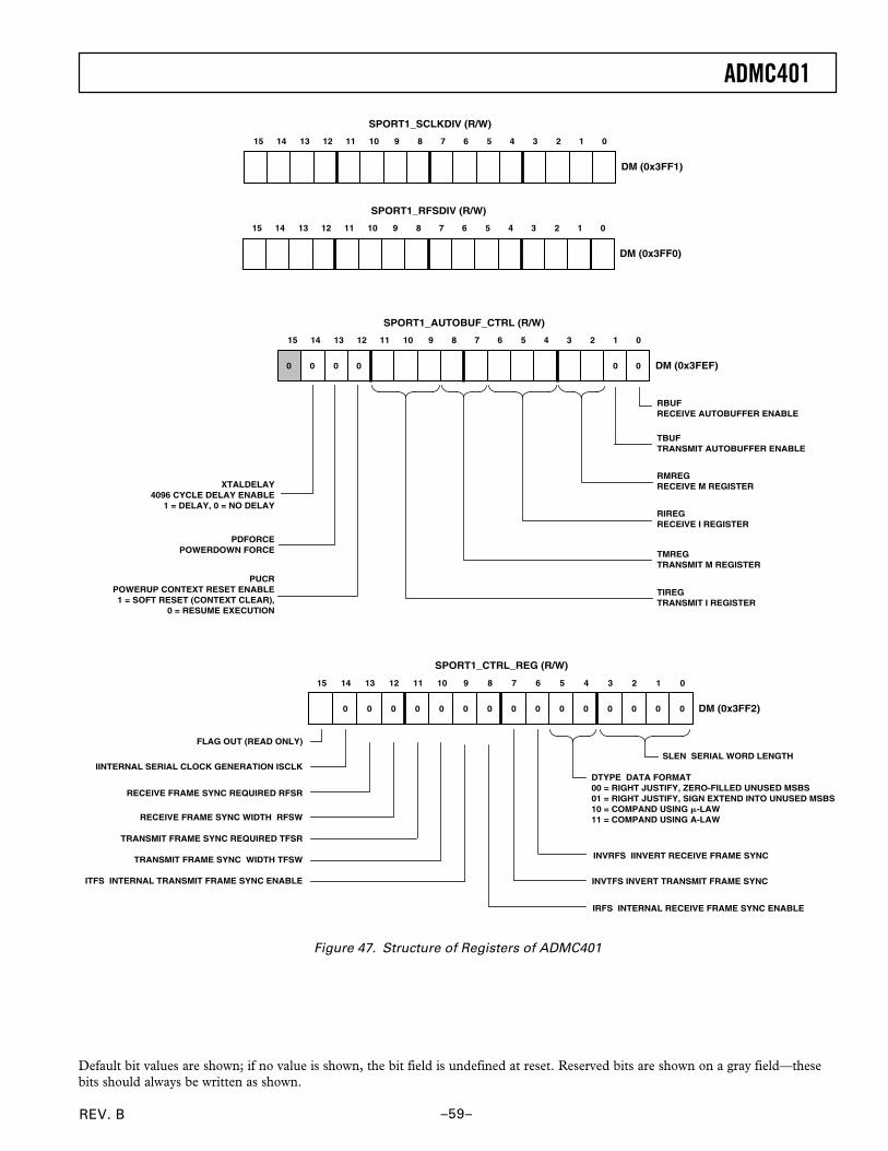
ADMC401
–59–REV. B
SPORT1_SCLKDIV (R/W)
15 14 13 12 11 10 9 8 7 6 5 4 3 2 1 0
DM (0x3FF1)
SPORT1_RFSDIV (R/W)
15 14 13 12 11 10 9 8 7 6 5 4 3 2 1 0
DM (0x3FF0)
RBUFRECEIVE AUTOBUFFER ENABLE
TBUFTRANSMIT AUTOBUFFER ENABLE
RMREGRECEIVE M REGISTER
RIREGRECEIVE I REGISTER
TMREGTRANSMIT M REGISTER
TIREGTRANSMIT I REGISTER
XTALDELAY4096 CYCLE DELAY ENABLE
1 = DELAY, 0 = NO DELAY
PDFORCEPOWERDOWN FORCE
PUCRPOWERUP CONTEXT RESET ENABLE1 = SOFT RESET (CONTEXT CLEAR),
0 = RESUME EXECUTION
SPORT1_AUTOBUF_CTRL (R/W)
15 14 13 12 11 10 9 8 7 6 5 4 3 2 1 0
DM (0x3FEF)0 0 0 0 0 0
SPORT1_CTRL_REG (R/W)
FLAG OUT (READ ONLY)
IINTERNAL SERIAL CLOCK GENERATION ISCLK
RECEIVE FRAME SYNC REQUIRED RFSR
RECEIVE FRAME SYNC WIDTH RFSW
TRANSMIT FRAME SYNC REQUIRED TFSR
TRANSMIT FRAME SYNC WIDTH TFSW
ITFS INTERNAL TRANSMIT FRAME SYNC ENABLE
SLEN SERIAL WORD LENGTH
DTYPE DATA FORMAT00 = RIGHT JUSTIFY, ZERO-FILLED UNUSED MSBS01 = RIGHT JUSTIFY, SIGN EXTEND INTO UNUSED MSBS10 = COMPAND USING -LAW11 = COMPAND USING A-LAW
0000000 00 000000
15 14 13 12 11 10 9 8 7 6 5 4 3 2 1 0
INVRFS IINVERT RECEIVE FRAME SYNC
INVTFS INVERT TRANSMIT FRAME SYNC
IRFS INTERNAL RECEIVE FRAME SYNC ENABLE
DM (0x3FF2)
Figure 47. Structure of Registers of ADMC401
Default bit values are shown; if no value is shown, the bit field is undefined at reset. Reserved bits are shown on a gray field—thesebits should always be written as shown.
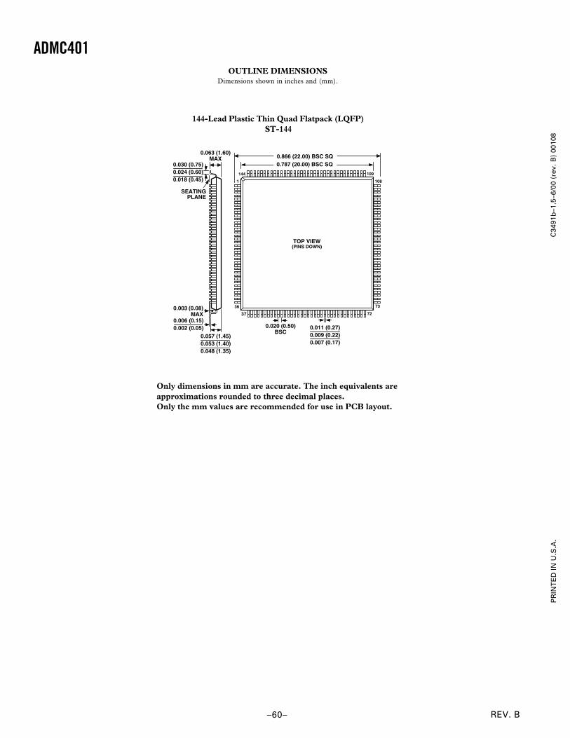
–60–
C34
91b
–1.5
–6/0
0 (r
ev. B
) 00
108
PR
INT
ED
IN U
.S.A
.
REV. B
ADMC401
144-Lead Plastic Thin Quad Flatpack (LQFP)ST-144
1
36
37
73
72
108
144 109
TOP VIEW(PINS DOWN)
0.787 (20.00) BSC SQ 0.866 (22.00) BSC SQ
0.020 (0.50)BSC
0.011 (0.27) 0.009 (0.22) 0.007 (0.17)
SEATINGPLANE
0.063 (1.60)MAX
0.030 (0.75)0.024 (0.60)0.018 (0.45)
0.006 (0.15)0.002 (0.05)
0.057 (1.45) 0.053 (1.40) 0.048 (1.35)
0.003 (0.08)MAX
OUTLINE DIMENSIONSDimensions shown in inches and (mm).
Only dimensions in mm are accurate. The inch equivalents areapproximations rounded to three decimal places.Only the mm values are recommended for use in PCB layout.