a constructal principle based optimal … optimal design for photovoltaic cell architectures 923 in...
TRANSCRIPT

A CONSTRUCTAL PRINCIPLE BASED OPTIMAL DESIGN FOR PHOTOVOLTAIC CELL ARCHITECTURES
AL. M. MOREGA, M. MOREGA
Department of Electrical Engineering, POLITEHNICA University of Bucharest,
313 Splaiul Independenţei, Bucharest 6, 77206, Romania [email protected], [email protected]
Received May 28, 2004
The ever increasing demand for miniaturized, fast, cheap systems and devices lead to fundamental changes in fabrication technologies that request new architectural principles for materials. The paper presents a constructal principle solution to optimized photovoltaic cells and modules design, applicable to other electrical, electronic and mechanical applications.
Key words: constructal principle, optimization, numerical model, finite element, photovoltaic cell.
1. INTRODUCTION
The contemporary global competitional pressures and the ever increasing demand for miniaturized, fast and cheap systems and devices lead to fundamental changes in the fabrication technologies, which request new materials with structres based on new architectonic principles. At macro, micro, sub-micro and nanometer levels the same optimal (signal, power, heat, protection) access problems from the system to its boundary ports through fast access paths occur.
In the realm of microelectronic devices and electronic packing, at the smallest scale of every microelectronic system there are integrated chips that are part of the functional system through a packaging hierarchy [2]–[11]. The ensemble (the package) provides for signal and power delivery, heat dissipation and system protection. Besides chips, the electronic ensemble is made of discrete and integrated devices (detectors, laser diodes, photonic or optoelectronic chips), which communicate through electrical or optical via, such as metallic or organic-metallic printed circuits. The chips comprise transistors and are provided with overlapping cabling paths for interconnection and coupling with the ensemble. As the number and diversity of these devices increases, the communication becomes more and more complex. The number of integration levels within a structure varies with the ensemble degree of integration. A typical high Rom. Journ. Phys., Vol. 49, Nos. 9–10 , P. 919–936, Bucharest, 2004

920 Al. M. Morega, M. Morega 2
performance ensemble hierarchy consists of chips, modules, printed circuits and gates. At each level, an optimal design is then needed, and optimization principles become design tools.
Magnetic recording devices are another important, expanding class of applications where the continuous miniaturization constantly requests new materials with superior properties [12]. Thin-film for magnetic memory, “on-wafer” processing, the controlled doping of Ni-Fe alloys, and more recently materials for giant magneto-resistances are several milestones that mark an evolution where the demand for new, optimal architectures is of major concern.
Microelectromechanical systems (MEMS) are miniaturized machines that include sensors, effectors and control. Their micro-fabrication on silicon substrate uses the technology developed for integrated circuits that embodies erosion and gluing processes to produce 3D structures at micrometer scale. The nano-technology advent is the next stage for MEMS miniaturization and may impact the future microelectronic devices [29]–[34].
Concluding, at each level (from macro- to nanometer scale) of engineering design the same optimal access problem is evident: the access (signal, power, heat, protection) from the system – ensemble, ensemble layer, components (e.g., chips), sub-components (e.g. transistors), materials (e.g., silicon wafers) – to the ports (terminals, sinks) through access paths of superior properties (electrical and thermal conductivity, speed, etc.) than the volume within which they reside. In this context, the constructal principle [1] may lead to optimal solutions (structures) that relay on phenomenological compliance with the functional purpose of the device.
The constructal principle was first identified in connection to thermal design problems posed by the ever-growing electronic packaging demand for small-size, high-power dissipative systems, but was soon found to be universal, acting both in the inanimate and animate worlds [1]. This principle, introduced here in connection to new, optimal architecture of systems with constrained flows produces systems that are adaptive, “intelligent”, optimal in the sense of the ensemble’s functionality, and respond the objective of “assembly-by-construction”. Due to its universality this process may be used both to obtain primary materials that are structurally optimized and in the construction of architectonic ensembles with optimized functions that comprise materials with special properties (e.g., thermo-electric, thermo-magnetic, piezo-electric, piezo-magnetic, piro-electric, piro-magnetic, etc.).
The first part of this report is concerned with the constructal architecture related to the physical models for heat and electrical current conduction flows. Objectives and constraints specific to the constructal optimization in multifunctional materials architecture are discussed. Next, we present the elemental system that produces higher order optimal constructs.

3 Optimal design for photovoltaic cell architectures 921
From a broader perspective, this report is aimed at applying the constructal principle in the construction of optimal structures for new materials for electrical, electronic and mechanical applications.
2. CONSTRUCTAL OPTIMIZATION
The theoretical development of the constructal principle, proposed here in the architecture of multifunctional materials, relies on the analysis of natural dynamic systems with flows, currents and gradients (e.g., temperature, pressure, electric potential, chemical potential, etc.) that, internally, are not at thermodynamic equilibrium, i.e., are not static. A second important aspect, the variety of geometrical natural forms that we may recognize and which are found in both animate and inanimate worlds is not that vast: natural systems may have the same geometric shape without being identical. For instance, two bronchial trees are never identical. Basically, when these systems are presented by a single image out of the endless diversity of natural flow forms we have the ability to recognize and classify them in one of the three forms: tree, round and slice. If one single principle is responsible of all these forms then this principle may act everywhere. It becomes a law that ties different areas such as physics and biology or, better said, two different modes of reasoning, two different points of view.
CONSTRUCTAL VERSUS FRACTAL ARCHITECTURE
Recently, many instances of macroscopic organization observed in nature were approached by fractal geometry analysis: images generated by repeating a set of rules several times may be projected to resemble a natural tree-like structure. However, the physical principle out of which the fractal algorithm may be deduced is not apparent: “the progress depends on establishing a more substantial theoretical basis where the geometric shape should emerge from the very principle that produces it” [13].
Fractal geometry promotes the idea that natural tree-like structures are fractal objects. Following this path, the fractal dimension given by Mandelbrot [14] is an object generated through ad infinitum repetition of an algorithm based on postulated similarity laws. This infinite sequence of branching or coalescence stages is remarkably absent from the natural tree-like systems. The designer has to cut off the fractal algorithm after a few steps (internal cut off) in order to be capable to observe the actual drawing of the resulting structure. If the natural structures would be really fractal, “we would observe nothing else than blurred images and gray nuances” [15], [16]. Why then is this internal cut off needed? Why does bifurcation (twinning) occur, and why the bifurcation law no longer applies to small scales? Further more, at small scales branching through

922 Al. M. Morega, M. Morega 4
bifurcation no longer occurs, and the number of branches per ramification increases (e.g., alveoli, the finest capillary vessels, the needles on the last branches). These facts suggest that ramification may be the outcome of an optimization process.
Seen from this perspective the constructal principle used in this work, as compared to the fractal alternative, produces architectures that are based on geometric structures emergent by optimization – purpose, function, optimal design – and not by conjectural assumptions. In some sense, the identification of a specific constructal structure may be interpreted as pattern analysis or pattern mining.
FUNCTIONAL OBJECTIVE AND CONSTRAINTS
Spatial and temporal structures observed in nature are the results of certain processes of global optimization subject to specific local and global constraints. This principle demands that a finite-size heterogeneous system undergoes changes in shape and structure such as to provide for an as easy as possible access (low resistance paths) of its internal currents.
The existence of some law of natural structure generation is not of surprise – optimization principles such as minimum travel time, minimum flow resistance, minimum power consumption are frequently and constantly invoked and used, and it is remarkable that these deterministic principles are independent, and do not follow up (do not result) from other, known laws.
The same principle may be used also to produce new structures for multifunctional materials. Engineering design starts by a clear understanding of the objective: the system mission, purpose, function and performance. This concept implies also optimization, because the designed system is expected to perform (function) the best possible. Possible means that the designer recognizes the local and global constraints (limitations) that the system may have. Some of the very common global constraints are the system mass and volume. The heat generated within the occupied volume, e.g., by an electronic ensemble, is another global constraint when the electronic components have fit within an imposed volume.
The local constraints are more subtle, but equally important. In a system with internal heat generation (e.g., a cable that carries electrical current, electronic devices, etc.) the maximum temperature is not to exceed a certain safe limit. The number and localization of the hot spots is not important. The local constraints are then gathered in an objective function defined at the system level. The geometry is the unknown. The external shape and the internal structure emerge then by successive designs (iterations) that comply with the global and local constraints, in the objective pursuit. The initial position that this engineering point of view occupies is essential to understand in a deterministic (predictive, anticipative) sense the emergence of shape and structure in natural systems.
5 Optimal design for photovoltaic cell architectures 923
In the constructal theory, the deterministic evolution occurs in time, from principle (engineering) to nature. The history of science and technology is reach in examples where the sense is the opposite, i.e. from nature to engineering – this method is recognized today as Biomimetics, and it continues to be a valuable instrument in engineering design. Compared to Biomimetics, constructal theory acts in the opposite sense: through the constructal law, the engineering generates a purely theoretic point of view, from which Nature may be better understood, i.e. more simply.
FERMAT’S PRINCIPLE AND CONSTRUCTAL PRINCIPLE
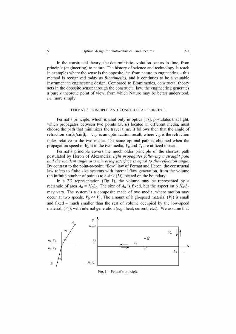
Fermat’s principle, which is used only in optics [17], postulates that light, which propagates between two points (A, B) located in different media, must choose the path that minimizes the travel time. It follows then that the angle of refraction ,sin sini r i rβ β = ν is an optimization result, where νi,r is the refraction index relative to the two media. The same optimal path is obtained when the propagation speed of light in the two media, V0 and V1 are utilized instead.
Fermat’s principle covers the much older principle of the shortest path postulated by Heron of Alexandria: light propagates following a straight path and the incident angle at a mirroring interface is equal to the reflection angle. By contrast to the point-to-point “flow” law of Fermat and Heron, the constructal law refers to finite size systems with internal flow generation, from the volume (an infinite number of points) to a sink (M) located on the boundary.
In a 2D representation (Fig. 1), the volume may be represented by a rectangle of area A0 = H0L0. The size of A0 is fixed, but the aspect ratio H0/L0 may vary. The system is a composite made of two media, where motion may occur at two speeds, V0 << V1. The amount of high-speed material (V1) is small and fixed – much smaller than the rest of volume occupied by the low-speed material, (V0), with internal generation (e.g., heat, current, etc.). We assume that
Fig. 1. – Fermat’s principle.

924 Al. M. Morega, M. Morega 6
A0 is that small as to include a single strip of high-speed material: A0 is then called elemental system. The volume-to-point access problem at A0 level is analyzed in detail.
The constructal law requests that the access between all points of A0 and M is maximized. The geometric shape, the external aspect ratio, H0/L0, and the internal structure of A0 (i.e., the distribution of high speed material throughout the low-speed material) are then natural results and we recognize all elements of objective and constraints: the objective of the finite-size system consists of maximizing the volume-to-point access.
The global constraints are the fixed size of the system and the amount of high permeability material that is to be distributed within the system. The local constraint intervenes through the fact that some of the internal points will always have easier access to M than other points. The longest trip to M is associated to the most distant point in A0 (point P in Fig. 1), which is then the most solicited point – it is the analogous to the point of highest mechanical stress in a mechanical structure or the hottest spot in a thermal structure. The design may be improved by changing the external aspect ratio, to produce more uniform working conditions, i.e. uniform access to the volume from M.
The constructal principle focuses on the whole, and the optimization process works similarly to Fermat’s principle that anticipates the geometric shape of the light beam. Unlike Fermat’s principle where the trajectory is broken at the interface between the two semi-infinite media, in the volume-to-point access problem the bent (e.g., R) is found on the central axis of A0, and this is the result of an optimization principle. The volume-to-point construct is then a bundle of an infinite number of flow paths that verifies Fermat’s principle.
At this point we may introduce the fundamental constructal problem: “Given a finite size volume with internal heat generation and of
low conductivity, which is cooled by a small-size sink placed on the boundary, distribute a fixed amount of high conductivity material within the volume such that the hotspot temperature is minimum” [1]. In other words, find the collector structure that minimizes the system’s global thermal resistance. For instance, electronic structures (packages) are subject to thermal
objectives and constraints. The global constraint is the finite volume where the system must fit. The thermal design objective consists of installing as many components as possible, hence an as high as possible heat generation rate, q (electrical structures generate heat). The maximum temperature in the systems may not exceed a specified limit, Tmax – this is the local constraint. The optimal design is then superior if q is large, i.e. the global thermal conductance q/(Tmax –– T0) is high – T0 is the initial temperature of the environment that absorbs the heat. This problem is presented next for the electrical optimization of PVC [27].

7 Optimal design for photovoltaic cell architectures 925
3. CONSTRUCTAL OPTIMIZATION OF PVC
Photovoltaic cells (PVC) are semiconductor, p–n devices that convert light directly into electricity. The “particles” of light (photons) absorbed by the PVC wafer generate electric charges (electrons and holes) that are drained across the p-n junction in opposite directions by the action of an electric field produced at the interface. This segregation generates a voltage across the junction that produces a current in an external load [35], [48].
PVC efficiency is diminished by the partial reflection of the incident light, the incomplete absorption and utilization of the photons energy, the partial recombination of electrical charge carriers and the leakage across the junction [43]–[46]. The power loss occurs in the bulk of the base material, Rp (Fig. 2,a), in the narrow top-surface layer, at the interface between the cell and the electric terminals used to connect the PVC to an external electrical circuit [36].
a. Equivalent PVC scheme
b. The effect of Rp and RS c. The maximum power point.
Fig. 2. – Equivalent circuit for a crystalline, heterojunction PVC.
The cell series resistance, RS (Fig. 2,a), met by the lateral current in the cell’s top layer is responsible for the flattening of the current-voltage characteristic (Fig. 2,b) and for the pending PVC output power loss. It may be reduced by using a highly conductive material for the top layer, by increasing its thickness, by good galvanic contacts and by optimized geometry for the contact grid [37], [48].
The optimization of RS consists of minimizing the sum of the collector shadow and resistance losses and, despite the many physical processes within the

926 Al. M. Morega, M. Morega 8
PVC [41] it may be conducted separately [38]. Instead of the double diode description of the PVC, we use the simpler maximum power point (MPP) approach (Fig. 1,c) [43]. This allows for the PVC to be optimized either for a specific or for a mix of irradiation levels, such as it occurs under normal working conditions.
OPTIMAL COLLECTOR GRID DESIGN CONCERNS
The collector – a finger-like metallic contact connected to a metallic busbar system – is to collect current and to reduce RS. Unfortunately, this structure prevents for the incident radiation to reach the cell: although large electrical contacts minimize RS, they also cover the cell and block too much of the light. An optimal design is then a compromise between an as low as possible RS (closely spaced, highly conductive grid fingers with good adhesion and low RS) and an as high as possible light transmission (fine, widely spaced fingers). Currently, the acceptable loss from the contact shading is 10% in commercial cells [37], [48–49]. The optimal design of the collector has to comply also with criteria such the aesthetic appearance, and several collector patterns derived from the H-type PVC were proposed [38]. Fig. 3 shows a pin-up (PUM) module optimized with respect to its series resistance [18]. Other examples of optimized dissipative structures cooled by free and forced convection may be found in [19]–[28].
Fig. 3. – PinUp PVC Module (PUM) [18].
The basic constructal volume-to-point access problem is equivalent to finding the particular collector pattern (high conductivity material) that minimizes the equivalent thermal resistance of the volume, or the design goal of reducing RS for the heterojunction PVC with metallic electrode on the illuminated face (emitter). In this sense the results reported here translate previous, thermal analysis results [40] into electrical terms, specific to the PVC design.
The elemental system
We assume that the PVC operates under DC conditions hence the associated electric field is derived from the electric potential, V. For PVC with

9 Optimal design for photovoltaic cell architectures 927
very thin emitter and collector the current flow in the emitter and metallic grid is 2D. The mathematical model for the electric field is then made of the following equations,
2 2
2 2 00,V V w
x y′′′∂ ∂+ + =σ∂ ∂
emitter (1a)
2 2
2 2 0,V Vx y
∂ ∂+ =∂ ∂
metallic collector (1b)
to which add appropriate boundary conditions (BC’s) ( is the photovoltaic current source).
w′′′
The constructal theory introduced by [39–40] is then readily applicable by using the equivalence ,T V↔ ,q w′′′ ′′′↔ 0 0 ,k ↔ σ p pk ↔ σ (kp, k0 and σp, σ0 are the thermal and electrical conductivities of the collector and emitter, respectively). The adiabatic boundaries in [40] are here electrically insulated surfaces. In the elemental system of Fig. 4 the metallic strip is placed on the horizontal symmetry axis. Except for the sink at the origin, the boundary is insulated.
Fig. 4. – The slender elemental volume with internal PV current generation and one metallic collector finger.
As the volume (W is the thickness, i.e. the third dimension) and the fraction of the volume occupied by the metallic grid, Vp, are fixed, the area of the shadowed part, which is covered by the finger, is kept constant throughout the optimization. H0 and L0 may vary, but is constant, and as
0 0V H L W=
0 0A H L= 0
00H L<< it follows that the current in the emitter flows mainly in y direction, to be then collected by the σp finger at and drained in x direction toward the origin.
0y =
Problem (1a) subject to 0 2 0y HV y =∂ ∂ = and has the
analytic solution
( ) (0,0V x V x= )
( ) ( ) ( )20 0 0, 2 ,V x y w H y y V x y′′′= σ − + . The current in the σp

928 Al. M. Morega, M. Morega 10
strip obeys the fin-like equation 2 20 d d 0PD V x w H′′′σ + 0 ,= and the boundary
conditions (0 0 0,0xV V= = ) and 0
0d d 0x LV x = = . The maximum voltage drop
on this elemental cell, ∆V0, occurs between the corners farthest from the origin, x = L0 and 0 2,y H= ± and it has a minimum with respect to the external shape (H0/L0),
1 2
0, 0 0
0 0 0 0
1 ,2 P
V Hw H L D
∆ σ⎛ ⎞= ⎜ ⎟′′′ σ σ⎝ ⎠min
1 20 0 0
0 02
Popt
H HL D
σ⎛ ⎞ ⎛ ⎞=⎜ ⎟ ⎜ ⎟σ⎝ ⎠ ⎝ ⎠. (2)
This result is consistent with the assumption that the elemental system is slender, suggesting that 0 0 0 1.P H Dσ σ >> >> Two additional properties of this geometric optimization are remarkable [40]: 1. The principle of equipartition: the voltage drop in the σ0 emitter equals the
voltage drop along the σp finger, i.e. the voltage drop is divided in half by the bend (x = L0, y = 0).
0,V∆ min
2. ( )20, 0 04V w H′′′∆ = σmin decreases at elemental level as This motivates
the effort to manufacture the smallest possible elemental system.
20 .H
First order construct
Fig. 5 shows the elemental system and the first order assembly, where the D0 strips are connected to the D1 busbar. The outer boundary is insulated, except for the terminal of size D1 at the origin where the collected current, leaves the structure.
1 1 ,w H L W′′′
Fig. 5. – The first order assembly made of elemental cells (systems).
The new optimization problem is to find how many elemental volumes to assemble, or the optimal external shape 1 1,H L× such that the maximum voltage drop from an internal point to the origin is minimal. Unlike the elemental system

11 Optimal design for photovoltaic cell architectures 929
where the current was assumed to flow in y direction, the current in the fingers is constrained to flow in y direction, independently of the construct shape. In a volume-averaged sense the construct behaves as the σ0 cell with an effective conductivity 1 0 .P D Hσ = σ 0 The constraint is the second equation.
1 0,2 optH L=
A similar analysis may be used to find ∆V1. Its maximum, between the farthest corner ( 1 1, 2L H ) and origin has a minimum, 2
1, 0 04 .V w H′′′∆ = σmin
If ( ) ( ) ( )1 4 1 4 1 21, 0 0 0 0 1 01 2opt pL H D H D H−= σ σ and ( )1 1 optH L =
( )( ) 1 21 1 12 P H D= ⎡ σ σ ⎤⎣ ⎦ then . 1 0V V∆ = ∆,min min,
The resistance of the assembly ( )1 1 1 0aV w H L′′′∆ σ
) is minimized for
constraint (1 ,1 1 1, ,p optA H Lφ = where is the
amount of σP material. For
,1 1 1, 1, 0 0,P opt opt optA D L n D L= +
( ) ( )1 2 3 21, 0 0 0 0opt PD H D H= σ σ it yields
( )1 02 0D Hφ = and ( )(1
2, 3 8 .aV w H′′′∆ = σmin )0 0 Apparently, the busbar has to
be wider than the fingers, ( ) ( ) 1 21 0 0 0 0 1.PoptD D D H= σ σ >>⎡ ⎤⎣ ⎦ An important
result is that the voltage drop on the optimized assembly is almost equal to the optimized voltage drop on the elemental system.
Next, a twice optimized first order assembly (with respect to the 1 1H L× shape and to the allocation of high conductivity material σP) is obtained for the
optimal number of fingers, ( )( ) 1 21, 0 0 0 1,opt Pn D H= ⎡ σ σ ⎤ >>⎣ ⎦ and for the
busbar length, ( )( )1 21, 0 0 01 2 .opt pL H D= σ σ Remarkably, the optimal shape of
this assembly is constant, ( )1 1 2,optH L = independent of the type of conducting
materials ( 0Pσ σ ) and of the proportion in which they are built into the assembly ( )1 .φ
Consequently, the optimal shape 1 1H L× is such that a square of side L1 forms on either side of the D1 busbar (x axis). By combining with
it yields 1 0,2 ,optH L=
( )1 0 1optL L = .
Second and third order constructs
The second order construct (Fig. 6) is made of two optimized first order constructs connected such that The D2 path needs not to 2 1 1, 22 2optH H L L= = = .

930 Al. M. Morega, M. Morega 12
Fig. 6. – Second order assembly: a square made of two optimized 1st order constructs. The D1 wide finger here is the D1 wide busbar in Fig. 5.
extend to the right boundary as this margin is insulated. The voltage drop on this assembly is
2 2 1,a D aV V V∆ = ∆ + ∆ min ( )2
21 0 ,aV w H′′′∆ σ
1
which – minimized with
respect to the material constraint – yields, 2 2 2, 2,P opt opt PA D L n A= +
02 1 2 0
12 1 ,3
DH
⎛ ⎞φ = +⎜ ⎟⎝ ⎠
2
20
, 1 2 0
3 118 3aw HV
′′′⎛ ⎞∆ = +⎜ ⎟ σ⎝ ⎠min (3a)
1 2 3 2
2, 01 20 0 0
4 .3
opt PD DH
σ⎛ ⎞ ⎛ ⎞= ⎜ ⎟ ⎜ ⎟σ⎝ ⎠ ⎝ ⎠H (3b)
This result is of the same order as for the first order construct and as for the elemental cell. The magnification factor of the busbar to the finger width is a constant, namely ( ) 1 2
2 1 4 3 2.31optD D = = .
The best third order ensemble is obtained by a double optimization (shape and busbar width) of a system made of optimized second order construct (Fig. 5). As the aspect ratio of the third order assembly and the length of its busbar are fixed – 3 22 ,H H= 3 2 2L H= – the only degree of freedom left is the busbar width, D3.
This quantity may be optimized in relation to the other widths of the metallization grid, (D2, D1, D0), and the overall voltage is
then minimized subject to the constraint For 3 3 ,a D aV V V∆ = ∆ + ∆ min
3 23 3 2P PA D L A= + .
( )(1 23 02 1 2 3 )0D Hφ = + and ( )( )( )
3
1 2 2, 03 8 1 2 3aV w′′′∆ = + σmin 0H it
yields ( ) ( )( ) ( )1 2 3 21 23, 0 0 0 08 3 .opt PD H D H= σ σ The magnification factor
of the busbar to the finger width is then double, 3, 2,2 .opt optD D=

13 Optimal design for photovoltaic cell architectures 931
Fourth and higher order ensembles
Fig. 8 shows the fourth order construct made of two third order constructs. and are listed in Table 1, line i = 4. Apparently, in the process of
optimization the finger width doubles, suggesting the following recurrence, 4,optD
4 ,aV∆ min
Table 1
The main parameters of the first six optimized assemblies
Assembly order i
Height factor 1/i iH H −
Shape* Finger width
factor 1/i iD D −
Length factor
1/i iL L − ,20 0
aiVw H∆′′′ σ
min 0
0i
HDφ
0
r 1
4 1
1 1/ 2
0
0 01pD
Hσ⎛ ⎞
>>⎜ ⎟σ⎝ ⎠ R
1/ 20
0 01pD
Hσ⎛ ⎞ >>⎜ ⎟σ⎝ ⎠
1 38 2
2 1 S 1/ 24 2.31
3= 1 ( )1 2
1 23 118 3
+ ( )1/ 2
1 212 1
3+
3 2 R 2 1 ( )1 2
1 23 218 3
+ ( )1/ 2
1 222 1
3+
4 1 S 2 2 ( )1 2
1 23 418 3
+ ( )1/ 2
1 242 1
3+
5 2 R 2 1 ( )1 2
1 23 618 3
+ ( )1/ 2
1 262 1
3+
6 1 S 2 2 ( )1 2
1 23 1018 3
+ ( )1/ 2
1 2102 13
+
* S = square; R = rectangle (shape factor = 2); r = rectangle (shape factor << 1)
1 2
0, 01 2 0 0
for 2.2 3
i pi opt i
DD D H ≥
σ⎛ ⎞= ⎜ ⎟σ⎝ ⎠
(4)
The finger path length and the height of the optimized construct obey similar doubling rules,
1 2
2 0 00
3,2 , even
2 , 5 2 , odd
i m pi iL H D m−
≥σ⎛ ⎞ ⎧
= ⎨⎜ ⎟σ ⎩⎝ ⎠
ii
= , (6)
1 2
02 00 0
2,1 , even
2 , 1 2 , odd
i p pi i
DH H pH
−≥
σ⎛ ⎞ ⎧= ⎨⎜ ⎟σ ⎩⎝ ⎠
ii
= . (7)

932 Al. M. Morega, M. Morega 14
Fig. 7. – Third order construct made of two second order constructs.
Fig. 8. – The best, fourth order construct.
The voltage drop for higher order assemblies and the porosity are then,
20
,min0 0 0
316i
ia
w HV D H′′′φ∆ = σ . (8)
( )
( )2 2 0
1 1 2 0
0 , even2 , 3 , 1 2 , odd3
i ri i
D i rH−
−⎧
φ = φ + ≥ = ⎨⎩
ii
(9)
Table 1 lists the constructal optimization results for higher order ensembles (fifth and sixth). The second and higher order ensembles are close to optimal (3).
Fig. 9 shows a detailed view of the optimized fourth assembly with its constituents, including the elemental cells (strips).
The number of such striations is not a constant, it is function of ( )1 2
0 0 02 PH Dσ σ . Another important feature is that the width of the optimized busbar increases with the assembly order.
Fig. 9. – Fourth order construct. Fig. 10. – Higher-order constructs.

15 Optimal design for photovoltaic cell architectures 933
Fig. 10 shows the high order end of the optimized construction sequence, where all features are determined by the constructal, deterministic method.
Fig. 11 shows the results obtained by full numerical FEM simulation for the first four ensembles. We used the FEMLAB multiphysics package [50] that implements a Galerkin finite element model on unstructured, Delauney meshes. Other structures, based on different geometries (e.g., circular) for the elemental cell are under current investigation.
a. Elemental system b. Second construct c. Third construct d. Fourth construct
Fig. 11. – Voltage (gray scale, isolines) and current (vectors) distributions for σ p /σ0 = 100.
4. CONCLUSIONS
The main conclusions drawn in this work are as follows:
• The constructal principle, applied here to the PVC design, is deterministic, and it relies on the usage of physical laws: the PVC is constructed starting from the smallest, elemental cell, by using optimized (on physical grounds) higher order building blocks, in a time arrow that spans from small to large [1], [40]. This technique differs fundamentally from a fractal, non-deterministic (i.e. postulated) top-down design that indefinitely repeats a unique pattern (e.g., through bifurcations), at lower and lower levels, from a macro assembly to lower and lower level PVC ensembles.
• As a general rule, the optimized PVC ensemble was built such that its structure provides easier access to the imposed (global) currents that flow through it.
• In the optimized PVC the total current is driven to the (terminals) with the smallest voltage drop, which results also in the smallest power loss by the series resistance.
• The first step in the constructal optimization is the elemental system that is optimized by applying basic (here Maxwell) physical laws.
• Starting with the second order construct one particular rule emerges: each new construct is made of two lower order (higher level of detail) constructs.

934 Al. M. Morega, M. Morega 16
• The third order construct is the last one that needs a separate analysis. As its structure differs from its smaller, second order constituents, its geometry cannot be obtained by recurrence formulas.
• Although not optimal in the mathematical sense, the PVC constructs of order higher than two are the best blocks that fit together.
• The present analysis is valid when the conductivities ratio 0 1Pσ σ >> and when the porosity, 1iφ << .
• The constructal minimization of RS leads to a design that is not only optimal: it has also an attractive, natural appeal, where the collector fingers evolve naturally into busbars. Therefore, depending on the elemental system, the optimized PVC structures may satisfy with the aesthetic criteria requested by architectural and design goals.
REFERENCES
1. A. Bejan, Shape and structure, from engineering to nature, Cambridge Univ. Press, 2000. 2. IBM J. Res. Develop. 41, No. 1/2, January/March 1997. 3. IBM Research magazine, No. 4, 16–21, 1997. 4. M. Datta, R. V. Shenoy, C. Jahnes, P. C. Andricacos, J. Horkans, J. O. Dukovic, L. T.
Romankiw, J. Roeder, H. Deligianni, H. Nye, B. Agarwalla, H. M. Tong, and P. A. Totta, J. Electrochem. Soc. 142, 3779, 1995.
5. J. H. Lau, Flip Chip Technologies, McGraw-Hill Book Co., Inc., New York, 1996. 6. L. T. Romankiw, Electrochim. Acta 42, 2985, 1997. 7. P. C. Andricacos and L. T. Romankiw, in Advances in Electrochemical Science and Engineering,
Vol. 3, H. Gerischer and C. W. Tobias, Eds., VCH Publishers, Inc., New York, p. 230, 1994. 8. T. Osaka, Electrochim. Acta 42, 3015, 1997. 9. N. F. de Rooij, in Micromachining and Microfabrication Process Technology III,
S.-C. Bellingham, WA, pp. 2–9, 1997. 10. P. J. McWhorter, A. B. Frazier, and P. Rai-Choudhury, in Handbook of Microlithography,
Micromachining and Microfabrication, Vol. 2, P. Rai-Choudhury, Ed., Society of Photo-Optical Instrumentation Engineers, Bellingham, WA, pp. 3–40, 1997.
11. W. Bacher, K. Bade, K. Leyendecker, W. Menz, W. Stark, and A. Thommes, in Electrochemical Technology, N. Masuko, T. Osaka, and Y. Ito, Eds., Kodansha Ltd., Tokyo, p. 159, 1996.
12. E. Chassaing, P. Nallet, M. Walls, and M. J. Hytch, in Magnetic Materials, Processes and Devices IV, L. T. Romankiw and D. Herman, Eds., PV 95–18, The Electrochemical Society, Pennington, NJ, p. 125, 1996.
13. L. P. Kadanoff, Fractals: where’s the physics? Phys. Today, Feb. pp. 6–7, 1986. 14. B. B. Mandelbrot, The fractal geometry of Nature, Freeman, New York, 1982. 15. A. Bejan, Advanced engineering thermodynamics, 2nd ed. Wiley, New York, 1997. 16. D. Avnir, O. Biham, D. Lidar, and O. Malcai, Is the geometry of Nature fractal? Science, 279,
pp. 39–40, 1998. 17. D. S. Lemmons, Perfect form, Princeton Univ. Press, Princeton, NJ, 1997. 18. PUM module. 19. Al. M. Morega, A. Bejan, and S. W. Lee, Free stream cooling of a stack of parallel plates, Int.
J. of Heat and Mass Transfer, 38, no. 3, pp. 519–531, 1995. 20. Al. M. Morega, J. V. C. Vargas, and A. Bejan, Optimization of pulsating heaters in forced
convection, Int. J. of Heat and Mass Transfer, 38, no. 16, pp. 2925–2934, 1995.
17 Optimal design for photovoltaic cell architectures 935
21. A. Bejan and Al. M. Morega, The optimal spacing of a stack of parallel plates cooled by turbulent forced convection, TN, Int. J. of Heat and Mass Transfer, 37, pp. 1045–1048, 1994.
22. Bejan, A. A. Bejan, S. J. Kim, Al. M. Morega, and S. W. Lee, The cooling of stacks of boards shielded by porous screens, Int. J. Heat and Fluid Flow, 1994, publicat (anexat scrisoare de la editor).
23. Al. M. Morega and A. Bejan, The optimal spacing of parallel boards with discrete heat sources cooled by laminar forced convection, Numerical Heat Transfer A, Applications, 25, pp. 373–392, 1994.
24. A. Bejan and Al. M. Morega, Optimal arrays of pin fins and plate fins in laminar forced convection, J. Heat Transfer, 115, pp. 75–81, 1993.
25. A. Bejan, Al. M. Morega, S. W. Lee, and S. J. Kim, The cooling of a heat generating board inside a parallel-plate channel, Int. J. Heat and Fluid Flow, 14, 2, pp. 170–176, 1993.
26. Al. M. Morega, and A. Bejan, The constructal approach to optimization volume to point conduction problems, 1st Workshop on Mathematical Modeling of Environmental Problems, Romanian Academy, Proceedings, pp. 97–111, Ed. Academiei, ISBN 973-27-0934-0, 2002.
27. Al. M. Morega and A. Bejan, A Constructal Approach To The Optimal Design Of Photovoltaic Cells And Modules, OPTIM 2002, May 16–17, Brasov, p. 251–256, 2002.
28. Al. M. Morega and A. Bejan, Constructal optimal design of the busbar and fingers network for photovoltaic cells and modules, ATEE’2000 Conference, POLITEHNICA Univ. of Bucharest, December 2000.
29. Elbio Dagotto, G. Alvarez, S. L. Cooper, A. L. Cornelius, A. Feiguin, J. Fernandez-Baca, D. Gibbs, J. P. Hill, T. Hotta, Nanoscale Phase Separation and Colossal Magnetoresistance, Springer Verlag, 2003, ISBN: 3540432450.
30. C. N. Borca, B. Xu, T. Komesu, H.-K. Jeong, M. T. Liu, S. H. Liou, S. Stadler, Y. U. Idzerda and P. A. Dowben – Electronic Structure Modifications Induced by Surface Segregation in La0.65Pb0.35MnO3 Thin Films, Europhys. Lett., 56 (5), p. 722–728, 2001.
31. G. Binasch, P. Grünberg, F. Saurenbach and W. Zinn, Enhanced magnetoresistance in layered magnetic structures with antiferromagnetic interlayer exchange, Phys. Rev. B 39, 4828, 1989.
32. J. L. Makous, J. A. Leavitt, L. G. McIntyre, Jr. L. Maritato, R. Vaglio, A. Cuccolo, and C. M. Falco, in T. W. Barbee, Jr., F. Spaepen, and L. Greer, editors, Multilayers: Synthesis, Properties, and Nanoelectronic Applications, Materials Research Society, Pittsburgh, PA. 103, 1988.
33. Technical Proceedings of the 2003 Nanotechnology Conference and Trade Show, Febr. 2003, San Francisco, Chapter 6, LAB-ON-CHIP.
34. S. Tumansky, Thin Film Magnetoresistive Sensors, IOP Publishing Ltd., 2001. 35. www.pv.unsw.edu.au/info/solarcel.html, Centre for Photo-voltaic Engineering UNSW, Solar
cells, Univ. of New South Wales, Australia. 36. www.starfire.ne.uiuc.edu/~ne201/1996/pradosev/major.html Solar energy research institute,
Photovoltaics Technical Information Guide, Sc Ed. 37. www.starfire.ne.uiuc.edu/~ne201/1996/pradosev/technical.html, Treble, F.C., Ed. Generating
electricity from the sun, Univ. of Illinois at Urbana Champaign. 38. www.ati.ac.at/~summweb/mradike/2psvsec.htm, Radike, M., Summhammer, J., Breymesser,
A. and Schlosser, V., “Optimization of artistic contact patterns on multicrystalline silicon solar cells”, 2nd Photovoltaic Solar Energy Conference, Vienna, Austria, 1998.
39. A. Bejan, “The constructal law of structure formation in natural systems with internal flows”, AES, vol. 37, Proc. Of the ASME, Advanced Energy Systems Division, ASME, pp. 257–264 1997.
40. A. Bejan, “Constructal-theory network of conducting paths for cooling a heat generating volume”, Int. J. Heat Mass Transf., vol. 40, no. 4, pp. 799–816, 1997.
41. P. P. Altermatt, G. Heiser, T. Kiesewetter, K. R. McIntosh, Ch. B. Honsberg, S. R. Wenham, and M. A. Green, Establishing an accurate numerical model for the 2D-simulation of

936 Al. M. Morega, M. Morega 18
buried contact cells, The 26th IEEE Photovoltaic Specialist Conference, Anaheim, CA, 29 September – 3 October, 1977.
42. D. Travers, M. Watt, I. MacGill, J. Kaye, S. Kunzi, and T. Spooner, Evaluation tool for building integrated photovoltaic systems, Photovoltaics Special Research Center, School of Electrical Engineering, Univ. of New South Wales, Sydney, NSW, Australia.
43. A. R. Burgers, and J. A. Eikelboom, “Optimizing metalization patterns for yearly yield”, 26th PVSC, Sept. 30 – Oct. 3, 1997, pp. 219–222, Anaheim, CA.
44. J. Horzel, and K. De Clerq, “Advantages of a new metallization structure for the front side of solar cells”, in 13th EC Photovoltaic Solar Energy Conference, Nice, France, pp. 1368–71, 1995.
45. M. Verbeek, and A. Metz, “Mechanically grooved high-efficiency Si solar cells with self-aligned metallization”, in the 25th IEEE Photovoltaic Specialists Conference, Washington DC, United States, pp. 521–524, 1996.
46. M. Green, Solar Cells: Operating Principles, Tech. & Systems Applications, U. South Wales, 1986.
47. A. Bejan, Heat Transfer, Wiley, New York, 1993. 48. http://emsolar.ee.tu-berlin.de/~ilse/solar 49. http://starfire/ne.uiuc.edu/~ne201/1996/pradosev 50. Comsol, A.B., FEMLAB v.23.b, 2003.