a comparative analysis of low power and area efficient … · · 2013-09-27multiplexer in...
TRANSCRIPT
A Comparative Analysis of Low Power and Area Efficient Digital Circuit
Design
1B. Dilli Kumar,
2A. Chandra Babu,
2V. Prasad
1Assistant Professor, Dept. of ECE, Yoganada Institute of Technology & Science, Tirupati, India
2Assistant Professor, Dept. of ECE, Yoganada Institute of Technology & Science, Tirupati, India
2Assistant Professor, Dept. of ECE, Shree Institute of Technical Education, Tirupati, India
Abstract
Low power consuming devices are playing a
dominant role in the present day VLSI design
technology. If the power consumption is less, then the
amount of power dissipation is also less. The power
dissipation of a device can be reduced by using
different low power techniques. In the present paper
the performance of 4x1 multiplexer in different low power techniques was analyzed and its power
dissipation in those techniques is compared with the
conventional CMOS design. Each of these techniques
has different advantages depending on their logic of
operation. The simulation results show that the
proposed techniques have less power dissipation
compared to the conventional CMOS with reduction
in area also.
Keywords- Low power, Power dissipation, GDI, PTL, Adiabatic, Charge recovery
1. Introduction
The need for low power devices has been
increasing rapidly. As many of the present day
electronic devices are portable, they need more
battery backup which can be achieved only with the
low power consumption circuits that are internally
designed in them. So energy efficiency has become
main concern in the portable equipment‟s to get
better performance with less power dissipation. As the power dissipation in a device increases then extra
circuitry is necessary to cool the device and to protect
the device from thermal breakdown which also
results in increase of total area of the device. In order
to overcome these problems the power dissipation of
the circuit is to be reduced by adopting different low
power techniques. The less the power dissipation, the
more efficient the circuit will be.
From the past few decades CMOS technology
plays a dominant role in designing low power
consuming devices. Compared to different logic
families CMOS has less power dissipation which
made it superior over the previous low power techniques. The power consumption in conventional
CMOS circuit is due to switching activity of the
devices from one state to another state and due to the
charging and discharging of load capacitor at the
output node. The power dissipation in conventional
CMOS design can be minimized by reducing the
supply voltage, node capacitance value and switching
activity. But reducing the values of these parameters
may degrade the performance of the device. So an
efficient low power technique other than CMOS is
needed that has less power dissipation compared to
CMOS.
In the present paper different low power techniques Dual Pass Transistor Logic (DPTL), Gate
Diffusion Input (GDI), and Adiabatic logic are
discussed and their performance is compared with
CMOS design. Simulation results shows that the
proposed technique is efficient over the conventional
CMOS design in terms of power dissipation.
2. Multiplexer
Multiplexer is a digital switch. It allows
digital information from several sources to be routed
onto a single output line. The basic multiplexer has
several data input lines and a single output line. The
selection of a particular input line is controlled by a
set of selection lines. Normally, there are 2n input
lines and n selection lines whose bit combinations
determine which input is selected. Therefore,
multiplexer is „many into one‟ and it provides the digital equivalent of an analog selector switch. The
4x1 multiplexer has four inputs and one output. In
addition, it has two selection lines. Depending on the
two selection lines, one output is selected at a time
from among the four input lines.
B Dilli Kumar et al, Int.J.Computer Technology & Applications,Vol 4 (5),764-768
IJCTA | Sept-Oct 2013 Available [email protected]
764
ISSN:2229-6093

Table 1: Truth table of 4x1 multiplexer
Fig 1: CMOS BCD to 4x1 Multiplexer
3. Low Power Techniques
Power consumption of a circuit can be
reduced by using different techniques depending on
the area of application.
3.1.1 Gate Diffusion Input (GDI)
GDI is an efficient alternative for
Conventional CMOS design in terms of area and
power dissipation. The GDI technique has less area
and less power dissipation compared to the CMOS
design. A basic GDI cell consists of four terminals- G (common gate input to both pMOS and nMOS
transistors), P (outer diffusion node of pMOS), N
(outer diffusion node of nMOS transistor), D
(common diffusion of both transistors). P, D and N
can be used as either inputs or outputs depending on
the circuit structure and its mode of operation.
Fig 2: Basic GDI Cell
By using GDI technique, it is possible to
reduce the transistor count, power dissipation,
propagation delay also. The 4x1 multiplexer can be
implemented using GDI technique as
Fig 2: 4x1 Multiplexer using GDI technique
3.1.2 Dual Pass Transistor Logic (DPTL)
A logic circuit can be optimized in terms
of power and area to a great extent by using DPTL
logic. It reduces the power dissipation and transistor
count of a logic circuit compared to CMOS design
which makes it suitable for low power and portable
applications. A basic DPTL cell contains pMOS and
nMOS transistors connected in parallel. The 4x1
multiplexer in DPTL logic can be designed as
Selection
lines
Inputs Output
S2 S1 A B C D
0 0 1 0 0 0 A
0 1 0 1 0 0 B
1 0 0 0 1 0 C
1 1 0 0 0 1 D
B Dilli Kumar et al, Int.J.Computer Technology & Applications,Vol 4 (5),764-768
IJCTA | Sept-Oct 2013 Available [email protected]
765
ISSN:2229-6093

Fig 3: 4x1 Multiplexer using DPTL technique
3.1.3 Adiabatic Logic
Adiabatic logic is based on charge recovery
principle. It reuses the energy which is dissipated
during the charging and discharging process of circuit operation. As the name itself indicates that instead of
dissipating the stored energy during charging process
at the output node towards ground it recycles the
energy back to the power supply thereby reducing the
overall power dissipation and hence the power
consumption also decreases. The adiabatic logic uses
AC power supply instead of constant DC supply, this
is one of the main reasons in the reduction of power
dissipation. The basic 4x1 multiplexer can be
constructed using adiabatic logic as
Fig 4: 4x1 Multiplexer using Adiabatic Logic
4. Simulation results and Discussion
The simulation results were verified using
HSPICE simulation software. The simulation results
of 4x1 multiplexer in conventional CMOS design and
different low power techniques were presented in this
section.
Fig 5: Simulated Waveforms in CMOS design
Fig. 5 shows the simulated results of 4x1 Multiplexer in conventional CMOS design where the top two
signals indicate selection lines and the bottom two
signals indicate input and output signals respectively.
Fig 6: Simulated waveforms in GDI technique
Fig. 6 shows the simulated results of 4x1 Multiplexer
in GDI design where the top two signals indicate
selection lines and the bottom two signals indicate
input and output signals respectively.
B Dilli Kumar et al, Int.J.Computer Technology & Applications,Vol 4 (5),764-768
IJCTA | Sept-Oct 2013 Available [email protected]
766
ISSN:2229-6093

Fig 7: Simulated waveforms in DPTL
Fig. 7 shows the simulated results of 4x1 Multiplexer
in DPTL design where the top two signals indicate
selection lines and the bottom two signals indicate
input and output signals respectively.
Fig 8: Simulated waveforms in Adiabatic Logic
Fig.8 shows the simulated waveforms of 4x1
Multiplexer in Adiabatic Logic design, where the top
two signals indicate sinusoidal power clocks, the two
signals following it are selection lines and the bottom two signals are input and output signals respectively.
Table: 2: Comparison of Power dissipation of 4x1
Multiplexer in different low power techniques
S.No
Logic
Style
Power
Dissipation
(p Watts)
Transistor
Count
1. CMOS 408.0268 26
2. GDI 133.7856 6
3. DPTL 133.7856 6
4. Adiabatic
Logic
26.1855 28
Table 2 shows the power dissipation and transistor
count of 4x1 multiplexer in different low power
techniques. The adiabatic logic has less power
dissipation compared to other design styles and
DPTL and GDI has less transistor count compared to
other design styles. Depending upon the area of
application and circuit structure an appropriate design
style can be used to reduce the power dissipation and area.
5. Conclusion
This paper proposes different low power
techniques that can be used for the digital circuits.
The results were simulated using HSPICE and
comparison has been done for different parameters of
4x1 Multiplexer in different low power techniques
and CMOS design. The results show that the
proposed techniques has less power dissipation
compared to conventional CMOS design with less
transistor count. These advantages made these logics
more convenient for energy efficient digital
applications.
References
[1] B. Dilli Kumar, M. Bharathi, “Design of Energy Efficient Arithmetic Circuits Using Charge
Recovery Adiabatic Logic” in International
Journal of Engineering Trends and Technology,
2013.
[2] “Gate-diffusion input (GDI) – A technique
for low power design of digital circuits: Analysis and
characterization,” in Proc. Int. Symp. Circuits and
Systems (ISCAS), May 2002.
B Dilli Kumar et al, Int.J.Computer Technology & Applications,Vol 4 (5),764-768
IJCTA | Sept-Oct 2013 Available [email protected]
767
ISSN:2229-6093
[3] A. Morgenshtein, A. Fish, and I. A. Wagner,
“Gate-diffusion input(GDI) – A novel power efficient
method for digital circuits: A detailed
methodology,” in Proc. 14th IEEE Int. ASIC/SOC
Conf., Sept. 2001,pp. 39– 43.
[4] R. Zimmermann and W. Fichtner, \Low-
power logic styles: CMOS versus pass-transistor
logic," IEEE J. Solid-State Circuits, vol. 32, no. 7, pp. 1079{1090, Jul. 1997.
[5] K. Yano, Y. Sasaki, K. Rikino, and K. Seki,
“Top-down pass-transistor logic design,” IEEE J.
Solid-State Circuits, vol. 31, pp. 792–803,
June1996.
[6] A. P. Chandrakasan, S. Sheng, and R. W.
Brodersen, “Low- power CMOS digital design,”
IEEE J. Solid- State Circuits, vol. 27, pp.473–484,
Apr. 1992.
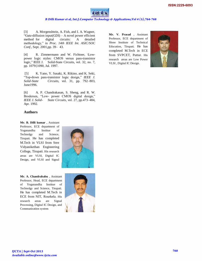
Authors
Mr. B. Dilli kumar , Assistant
Professor, ECE department of
Yoganandha Institue of
Technolgy and Science,
Tirupati. He has completed
M.Tech in VLSI from Sree
Vidyanikethan Engineering
College, Tirupati. His research
areas are VLSI, Digital IC
Design, and VLSI and Signal processing.
Mr. A. Chandrababu , Assistant
Professor, Head, ECE department
of Yoganandha Institue of
Technolgy and Science, Tirupati.
He has completed M.Tech in
ECE from NIT, Rourkela. His
research areas are SignaI
Processing, Digital IC Design, and
Communication system
Mr. V. Prasad , Assistant
Professor, ECE department of
Shree Institute of Technical
Education, Tirupati. He has
completed M.Tech in ECE
from SVPCET, Puttur. His
research areas are Low Power
VLSI , Digital IC Design.
B Dilli Kumar et al, Int.J.Computer Technology & Applications,Vol 4 (5),764-768
IJCTA | Sept-Oct 2013 Available [email protected]
768
ISSN:2229-6093