79 ghz pulse radar - epub.jku.at
TRANSCRIPT

AuthorAlexander Leibetseder, BSc
SubmissionInstitute for CommunicationsEngineering and RF-Systems
Thesis SupervisorUniv. Prof. Dipl.-Ing. Dr.Andreas Stelzer
Assistant Thesis SupervisorDipl.-Ing. Dr. Reinhard Feger
January 2016
JOHANNES KEPLERUNIVERSITÄT LINZAltenbergerstraße 694040 Linz, Österreichwww.jku.atDVR 0093696
79 GHz Pulse Radar
Masterarbeitto confer the academic degree of
Diplomingenieur
in the Masters Program
Information Electronics

Alexander Leibetseder, BSc: 79 GHz Pulse Radar, © January 2016

Part I
I N T R O D U C T I O N


0.1 A C K N O W L E D G E M E N T
This work was created at the end of my master’s program in the field of Information Electronics at the
Johannes Kepler University in Linz. In the course of my studies, I began to become interested in the de-
sign of integrated circuits and RF design. Therefore I would like to express special thanks to Univ. Prof.
Dipl.-Ing. Dr. Andreas Stelzer, who has enabled me to carry out this thesis at the Institute for Commu-
nications Engineering and RF-Systems. Also great thanks to our industry partner DICE GmbH & Co
KG for the fabrication of my chips and for the borrowed probes. My extraordinary gratitude deserves
Dipl.-Ing. Dr. Florian Starzer, without whose great personal commitment the entry into the field of in-
tegrated RF circuit design and the preparation of this thesis would have been impossible for me. No
less thanks goes to Dipl.-Ing. Dr. Herman Jalli Ng and Dipl.-Ing. Matthias Porranzl for their friendly and
patient support in all tasks that approached me. Last but not least I want to thank M.Sc. Faisal Ahmed,
M.Sc. Muhammad Furqan and Dr. Kambiz Hadipour for the numerous discussions which helped me
so much. I also want to thank Dipl.-Ing. Dr. Reinhard Feger and Dipl.-Ing. Thomas Wagner for the
great support in the theoretical aspects. Thanks also to the head of our technical group Ralf Ruders-
dorfer and to our secretary Monika Scheuchenegger for their helpfulness. At this point I would like to
thank my best friend, Sabrina Nömayr, for so many years of beautiful friendship.
The greatest thanks goes to my family and my girlfriend, Helena Pertl, for their indomitable support in
every walk of life.
Thank you
5


0.2 A B S T R A C T
The thesis presented here deals with the design and the characterization of a sequential sampling pulse
radar, where some building blocks partly existed at the institute. The radio frequency part of a conven-
tional continuous wave radar system is on for the whole duration of the measurement. In contrast to
that, a pulse radar system transmits only short pulses, where the pulse width is in the range of several
nano seconds. Thus, the high frequency part of a sequential sampling pulse radar can be switched off
in between the pulses. Hence, the power consumption of a sequential sampling pulse radar can be
significantly lower than the power consumption of a CW radar system with the same transmit power.
During the preparation of this work, the function of each component of the existing system has been
verified by simulation and ideas for improvements have been collected. Because the greatest poten-
tial for improvement is in the receive section, this section has been completely redesigned. The im-
provements have been verified by simulation first. Then each component of the radar system has been
characterized by measurements. Especially it could be shown, that the most crucial component of the
sequential sampling pulse radar, the pulse oscillator, works. It was the first time, as far as the author
knows, that the 77-GHz output signal of a periodically switched pulse oscillator was made visible in
time domain. Beside the hardware, this thesis also covers the derivation of a signal model for the se-
quential sampling pulse radar, which is then used to estimate the output signal of the system based on
the data from the simulation. Of special interest is the signal-to-noise ratio at the output, because this
limits the range of the system.
0.3 Z U S A M M E N F A S S U N G
Die hier vorliegende Arbeit behandelt die Verbesserung und messtechnische Verifikation eines, teil-
weise bereits am Institut vorhandenen, Pulsradarsystems welches auf dem Prinzip der sequentiellen
Abtastung basiert. Im Gegensatz zu einem herkömmlichen Dauerstrichradarsystem, bei dem der Hoch-
frequenzteil während der gesamten Dauer der Messung eingeschalten ist, sendet ein Pulsradarsys-
tem sehr kurze Pulse, mit Pulsweiten im Bereich weniger Nanosekunden, aus. Bei einem Pulsradar
kann der Hochfrequenzteil deshalb in der Zeit zwischen den Pulsen komplett abgeschaltet werden.
Das äußert sich direkt in einem deutlich niedrigerem Stromverbrauch, bei gleicher Sendeleistung, ver-
glichen mit einem CW Radarsystem. Während der Anfertigung dieser Arbeit wurden die einzelnen
Komponenten des bestehenden Systems zunächst durch Simulationen überprüft und Ideen für Ver-
besserungen wurden gesammelt. Da das größte Verbesserungspotential im Empfangsteil liegt, wurde
dieser im Vergleich zu den vorhandenen Blöcken komplett überarbeitet. Die Verbesserungen wur-
den zunächst mittels Simulationen verifiziert, anschließend wurden Messungen an allen Komponen-
ten des Radarsystems durchgeführt. Insbesondere konnte nachgewiesen werden, dass die Kernkom-
ponente des Sequential Sampling Pulse Radars, der Pulsoszillator, funktioniert. Bei dieser Messung
wurde, soweit dem Autor bekannt ist, zum ersten Mal das 77-GHz Ausgangssignal eines periodisch
geschalteten Pulsoszillators im Zeitbereich sichtbar gemacht. Neben der Hardware wird in dieser Ar-
beit auch ein Signalmodell für das Sequential Sampling Puls Radar System hergeleitet, um dann mit
Hilfe der Daten aus der Simulation das Ausgangssignal schätzen zu können. Von besonderem Interesse
ist der Signal-zu-Rausch Abstand am Ausgang, da dieser die Reichweite des Systems beschränkt.
7


C O N T E N T S
i I N T R O D U C T I O N 3
0.1 Acknowledgement . . . . . . . . . . . . . . . . . . . . . . . . . . . . . . . . . . . . . . . . . . 5
0.2 Abstract . . . . . . . . . . . . . . . . . . . . . . . . . . . . . . . . . . . . . . . . . . . . . . . . 7
0.3 Zusammenfassung . . . . . . . . . . . . . . . . . . . . . . . . . . . . . . . . . . . . . . . . . 7
0.4 Motivation . . . . . . . . . . . . . . . . . . . . . . . . . . . . . . . . . . . . . . . . . . . . . . 11
ii T H E O R Y 13
1 P U L S E R A D A R P R I N C I P L E 15
1.1 Differentiation from other radar principles . . . . . . . . . . . . . . . . . . . . . . . . . . . 15
1.2 Block diagram . . . . . . . . . . . . . . . . . . . . . . . . . . . . . . . . . . . . . . . . . . . . 15
2 S I G N A L M O D E L 17
2.1 Pulse Radar Equations . . . . . . . . . . . . . . . . . . . . . . . . . . . . . . . . . . . . . . . 17
2.1.1 Time Diagrams . . . . . . . . . . . . . . . . . . . . . . . . . . . . . . . . . . . . . . . 21
2.2 Radar Equation . . . . . . . . . . . . . . . . . . . . . . . . . . . . . . . . . . . . . . . . . . . 23
2.3 Link Budget Analysis . . . . . . . . . . . . . . . . . . . . . . . . . . . . . . . . . . . . . . . . 25
iii H A R D W A R E 27
3 T E C H N O L O G Y 29
4 E X I S T I N G A P P R O A C H 31
4.1 Introduction . . . . . . . . . . . . . . . . . . . . . . . . . . . . . . . . . . . . . . . . . . . . . 31
4.2 Short Description . . . . . . . . . . . . . . . . . . . . . . . . . . . . . . . . . . . . . . . . . . 31
4.2.1 Input signals . . . . . . . . . . . . . . . . . . . . . . . . . . . . . . . . . . . . . . . . 31
4.2.2 Monoflop . . . . . . . . . . . . . . . . . . . . . . . . . . . . . . . . . . . . . . . . . . 32
4.2.3 Comparator . . . . . . . . . . . . . . . . . . . . . . . . . . . . . . . . . . . . . . . . . 32
4.2.4 Pulse oscillator . . . . . . . . . . . . . . . . . . . . . . . . . . . . . . . . . . . . . . . 32
4.2.5 Balun . . . . . . . . . . . . . . . . . . . . . . . . . . . . . . . . . . . . . . . . . . . . . 32
4.2.6 LO-buffer . . . . . . . . . . . . . . . . . . . . . . . . . . . . . . . . . . . . . . . . . . 33
4.2.7 LNA . . . . . . . . . . . . . . . . . . . . . . . . . . . . . . . . . . . . . . . . . . . . . . 33
4.2.8 Mixer . . . . . . . . . . . . . . . . . . . . . . . . . . . . . . . . . . . . . . . . . . . . . 33
4.2.9 Integrator . . . . . . . . . . . . . . . . . . . . . . . . . . . . . . . . . . . . . . . . . . 33
4.3 Summary . . . . . . . . . . . . . . . . . . . . . . . . . . . . . . . . . . . . . . . . . . . . . . . 33
5 T H E N E W D E S I G N 35
5.1 Introduction . . . . . . . . . . . . . . . . . . . . . . . . . . . . . . . . . . . . . . . . . . . . . 35
5.2 Block Diagrams . . . . . . . . . . . . . . . . . . . . . . . . . . . . . . . . . . . . . . . . . . . 35
5.3 Monoflop . . . . . . . . . . . . . . . . . . . . . . . . . . . . . . . . . . . . . . . . . . . . . . . 36
5.4 Comparator . . . . . . . . . . . . . . . . . . . . . . . . . . . . . . . . . . . . . . . . . . . . . . 38
9
10 C O N T E N T S
5.5 Pulse Oscillator . . . . . . . . . . . . . . . . . . . . . . . . . . . . . . . . . . . . . . . . . . . . 42
5.6 Mixer . . . . . . . . . . . . . . . . . . . . . . . . . . . . . . . . . . . . . . . . . . . . . . . . . 48
5.7 Link Budget Analysis . . . . . . . . . . . . . . . . . . . . . . . . . . . . . . . . . . . . . . . . 68
iv M E A S U R E M E N T R E S U LT S 75
6 M O N O F L O P 77
7 C O M PA R AT O R 81
8 C O M P L E T E C O N T R O L U N I T 83
9 P U L S E O S C I L L AT O R 85
9.1 Power Measurements . . . . . . . . . . . . . . . . . . . . . . . . . . . . . . . . . . . . . . . . 85
9.2 Frequency Domain . . . . . . . . . . . . . . . . . . . . . . . . . . . . . . . . . . . . . . . . . 85
9.3 Time Domain . . . . . . . . . . . . . . . . . . . . . . . . . . . . . . . . . . . . . . . . . . . . . 87
10 M I X E R 99
v S U M M A R Y 105
11 C O N C L U S I O N 107
12 N E X T TA P E O U T 109
12.1 Mixer . . . . . . . . . . . . . . . . . . . . . . . . . . . . . . . . . . . . . . . . . . . . . . . . . 109
12.2 Power amplifier . . . . . . . . . . . . . . . . . . . . . . . . . . . . . . . . . . . . . . . . . . . 109
13 F U T U R E W O R K 113
vi A P P E N D I X 115
A C H I P L AY O U T S 117
L I S T O F F I G U R E S 121
L I S T O F A B B R E V I AT I O N S 127
L I S T O F M AT H E M AT I C A L S Y M B O L S 129
Bibliography 131
0.4 M O T I VAT I O N 11
0.4 M O T I VAT I O N
In 1904, the first working radar system was invented by the German RF engineer, Christian Hülsmeyer.
Since that, the fields of application for radar systems has grown from the first long range radar system
for military use towards the short range radar systems in the automotive area. The trend in the devel-
opment of radar systems goes towards even higher frequencies and lower power consumption. The
radar systems which are used in the automotive sector are typically frequency modulated continuous
wave (FMCW) systems [1]. As the name suggests, the transmit signal is generated from a continuously
running oscillator, where the frequency is modulated e.g. with a linear ramp.
In such systems, the high frequency components are on for the whole duration of the measurement,
which causes a high power consumption on the one hand and limits the application possibilities for
mobile radar systems. In contrast to that, the proposed sequential sampling pulse radar system only
transmits very short pulses, where the pulse width is in the range of several nano seconds. In between
the pulses, the complete high frequency part of the system can be switched off. This contributes to
a significantly lower power consumption compared to a FMCW radar system with the same transmit
power. In contrast to the classical pulse radar as it is described for example in [1], the sequential sam-
pling pulse radar requires that the generated pulse sequence is coherent in order for the radar to work.
This means that the phase relation between the pulse carriers is fixed. With increasing frequency, it
becomes more and more difficult to achieve this property, because the period of the signal decreases
and hence an timing error which was acceptable for a lower frequency becomes irreconcilable with the
higher operating frequency. But coherency not only means higher demands on the design of the radar
circuit, it also means high requirements on the stability of the used control signal in terms of jitter. In
[2] it was shown that the requirements could be met for a 24-GHz system. At 77GHz, no such system
was published, to the author’s knowledge.


Part II
T H E O RY
In this part the theoretical fundamentals of the sequential sampling pulse radar and the
differences to other radar systems are introduced.


1P U L S E R A D A R P R I N C I P L E
In this chapter, the basic idea of the sequential sampling pulse radar is introduced and the differences
to other radar systems are discussed. Also, a signal model is derived and an estimation for the magni-
tude of the output signal is made.
1.1 D I F F E R E N T I AT I O N F R O M O T H E R R A D A R P R I N C I P L E S
There are two major classical radars techniques, the FMCW radar and the pulse radar. A detailed expla-
nation of them would by far exceed the boundaries of this work, but can be found for example in [3].
In this section, only a brief overview is given with the goal to point out the differences.
In the FMCW techniques, as the name suggests, the transmit signal is a frequency modulated signal.
Usually it is generated from a voltage controlled oscillator, where the oscillation frequency typically
follows a periodic, linear ramp. This so called frequency ramp is transmitted to a target, where it is re-
flected and received after some time delay. The delay causes a constant frequency difference between
the received signal and the transmit signal. A mixer then multiplies the received signal with the current
transmit signal. Amongst other components, the output of the mixer contains a signal at the frequency
difference. The available bandwidth therefore determines the resolution of the FMCW radar. This con-
cepts is easy to implement in hardware, but has the drawback, that it requires a lost of digital signal
processing. Another drawback is, that the whole radar system is continuously on and thus the power
consumption of such a radar system is quite high.
In contrast to the FMCW radar, the classical pulse radar approach uses an on-off-amplitude modula-
tion. Here, an oscillator generates the carrier frequency and a subsequent switchable power amplifier
is used to cut out pulses from the continuous wave. The average transmit power of the pulse radar is
therefore lower compared to the FMCW radar. The location of the reflecting target can be extracted out
of the time delay between the transmit signal and the LO signal. Especially for short range applications,
the time delay is very short and thus difficult to measure. A technique using two pulse sequences with
slightly different pulse repetition rates for the transmit signal and the LO signal can be used to over-
come this issue. Comparable to the scale of a caliper, it spreads the received signal in time and the
delay time can be measured with more precision. A drawback also in this radar is the high power con-
sumption, because the oscillator and the receive part are always on.
The sequential sampling pulse radar as proposed in [2], also uses the approach of transmitting a pulse
sequence, but the power consumption can be greatly reduced. The ideas is to switch off the whole RF-
path between the pulses. In order to work properly, this requires a fixed phase relation between the
pulses. This property is called coherency. As described in part iii, it is difficult to achieve this property.
1.2 B L O C K D I A G R A M
In Figure 1 the block diagram of the proposed pulse radar is shown. The left part of the diagram shows
a control unit which generates two rectangularly shaped signals with period times of TLO and TRX. The
pulse width is Tp. These signals are then used to switch the pulse oscillators on and off to produce
15

16 P U L S E R A D A R P R I N C I P L E
sTX(t)
∫
sLO(t) sRX(t)
sIF(t)
y(t)
r
To IF-stage
From control unit
Figure 1: Simplified block diagram of the proposed pulse radar. The pulse generators on the left hand side generatethe transmit signal and the LO signal. The transmitted signal is reflekted from a target on the right handside. The mixer multiplies the received signal with the LO signal and the resulting signal is then integratedover time.
a sequence of pulses. The angular oscillation frequency of the pulse oscillators is denoted as ω0. The
upper pulse oscillator generates the transmit signal sTX (t ), which is sent over an antenna to a radar
target at a distance r . At the radar target, the signal is reflected back to the receiving antenna forming
the receive signal sRX (t ). The pulse oscillator in the lower part of the diagram produces the LO pulse
sequence sLO (t ). The mixer then multiplies the received signal with the LO signal. The signal at the
output of the mixer, sIF (t ), is then forwarded to the time domain integrator, where the output signal
y (t ) is created. For each target, the output signal contains a pulse similar to the transmit pulses but
spread in time and with a different envelope. The detailed calculation is done in Section 2.1 and a
sketch of the signals can be seen in Figure 2. The position of the target is related to the time at which
the pulse maximum occurs in the output signal.

2S I G N A L M O D E L
The goal of this chapter is to investigate the performance of the idealized pulse radar as it is shown in
Figure 1. The first step is to derive a mathematical description of the signal at the output of the pulse
radar which is done in Section 2.1. The resulting signals are sketched in subsection 2.1.1. In Section
2.2 the radar equation is explained and integrated into the signal model. Finally, in Section 2.3, the
magnitude of the output signal is approximated and the radar target’s location is extracted.
2.1 P U L S E R A D A R E Q U AT I O N S
In order for the pulse radar to operate properly, the pulse repetition time for the LO sequence must
be different from the one of the transmit sequence. Without loss of generality it can be assumed that
TRX > TLO. The difference between the pulse repetition times, ∆T , is then given by
∆T = TRX −TLO. (1)
It can be assumed that ∆T ¿ τRT, where τRT is the round trip delay time of the transmit signal.
In this case, it is allowed to express τRT = n∆T where n is a positive integer.
Also, it is assumed that the pulses are sufficiently short to avoid overlapping of an LO pulse with more
than one RX pulse: Tp ¿ TLO and Tp ¿ TRX .
As a consequence, there is a point in time where an LO pulse perfectly overlaps with an RX pulse.
Without loss of generality, it can be assumed that this happens for the pulse with index 0 at time t = 0.
Also, there is a point in time, expressed as the index kmax of the corresponding pulse, where the pulses
are overlapping for the first time and for the last time. Because of the periodicity of the control signals,
these points in time are also periodic. For the following calculations only one such period is viewed.
The index of the last overlapping pulses is then given by
kmax =⌊
Tp
∆T
⌋. (2)
For symmetry reasons, the index of the first overlapping pulses is −kmax.
One pulse p (t ) can be expressed as an amplitude modulated signal p (t ) = e (t )sin(ω0t ), where e (t )
denotes the normalized envelope.
The envelope is limited in time to have a duration of Tp, which is expressed using the rect(t ) function
e (t ) = h (t )rect
(t
Tp
). (3)
In (3), h (t ) is the normalized envelope of the pulse which is not necessarily limited in time. One pulse
can then be expressed as
p (t ) = sin(ω0t )h (t )rect
(t
Tp
). (4)
17

18 S I G N A L M O D E L
Now the LO pulse sequence can be expressed as sum of such pulses
sLO (t ) =kmax∑
n=−kmax
p (t −nTLO) . (5)
In order to calculate the transmit signal, the time for the kth pulse of the transmit pulse sequence is
expressed as kTRX = kTLO +k∆T using TLO and ∆T .
Now the transmit signal can be written as
sTX (t ) = A0
kmax∑n=−kmax
p (t −nTLO −n∆T ) , (6)
where A0 is the amplitude of the transmit pulses.
The received signal can be expressed as the transmit signal, appearing after the round trip delay time
at the receiving antenna. In addition, the signal is attenuated according to the description in Section
2.2. The attenuation is taken into account with the round trip gain factor αRT
sRX (t ) =αRTsTX (t −τRT) = (7)
sRX (t ) = A0αRT
kmax∑n=−kmax
p (t −τRT −nTLO −n∆T ) . (8)
The mixer is modeled as a multiplier with a voltage gain of αM.
The signal at the mixer output can be written as
sIF (t ) =αMsLO (t ) sRX (t ) . (9)
After inserting the signals (5) and (8) into (9), the output signal of the mixer is
sIF (t ) = A0αRTαM
(kmax∑
n=−kmax
p (t −nTLO)
)(kmax∑
m=−kmax
p (t −τRT −mTLO −m∆T )
). (10)
Because of the assumptions made above, only pulses with equal indexes n = m can overlap. The prod-
uct for pulses with unequal indexes is zero and the equation can be simplified to
sIF (t ) = A0αRTαM
kmax∑k=−kmax
p (t −kTLO) p (t −τRT −kTLO −k∆T ) . (11)
Inserting the pulse function (4) leads to
sIF (t ) = A0αRTαM
kmax∑k=−kmax
sin(ω0 (t −kTLO))sin(ω0 (t −τRT −kTLO −k∆T ))h (t −kTLO)×
×h (t −τRT −kTLO −k∆T )rect
(t −kTLO
Tp
)rect
(t −τRT −kTLO −k∆T
Tp
). (12)
Utilizing the following trigonometric identity
sin(x)sin(y)= 1
2
(cos
(x − y
)−cos(x + y
)), (13)
which can be found e.g. in [4] and the following equation

2.1 P U L S E R A D A R E Q U AT I O N S 19
rect
(t −kTLO
Tp
)rect
(t −τRT −kTLO −k∆T
Tp
)= rect
(t −τRT −kTLO −k ∆T
2
Tp −τRT −|k|∆T
), (14)
gives an equation for the output signal of the mixer
sIF (t ) = A0αRTαM
kmax∑k=−kmax
1
2(cos(ω0 (k∆T +τRT))−cos(2ω0 (t −kTLO)−ω0k (∆T −τRT)))×
×h (t −kTLO)h (t −τRT −kTLO −k∆T )rect
(t −τRT −kTLO −k ∆T
2
Tp −τRT −|k|∆T
). (15)
To simplify (15), it is assumed that the portion with twice the carrier frequency is attenuated so much
by the limited bandwidth of the mixer and the following integrator, that it can be neglected
sIF (t ) ≈ A0αRTαM
2
kmax∑k=−kmax
cos(ω0 (k∆T +τRT))h (t −kTLO)×
×h (t −τRT −kTLO −k∆T )rect
(t −τRT −kTLO −k ∆T
2
Tp −τRT −|k|∆T
). (16)
Following the block diagram of the pulse radar, the output signal of the mixer is now forwarded to an
ideal integrator, which produces the output signal of the pulse radar
y (t ) =t∫
−∞sIF
(t ′
)dt ′. (17)
Inserting (16) into (17) results in
y (t ) = A0αRTαM
2
t∫−∞
kmax∑k=−kmax
cos(ω0 (k∆T +τRT))h(t ′−kTLO
)h
(t ′−τRT −kTLO −k∆T
)××rect
(t ′−τRT −kTLO −k ∆T
2
Tp −τRT −|k|∆T
)dt ′. (18)
Between the pulses, the output signal has a constant voltage level. Because of the made assumptions,
y (t ) can be viewed as sum of step functions. So the output signal can be further simplified by sampling
it after the transitions. This means, that the signal is evaluated at the following points in time
t = nTLO + Tp
2. (19)
Inserting (19) into the output signal (18) leads to the sampled output signal, where n denotes the index
of the pulses

20 S I G N A L M O D E L
y [n] = y
(nTLO + Tp
2
)
= A0αRTαM
2
nTLO+ Tp2∫
−∞
kmax∑k=−kmax
cos(ω0 (k∆T +τRT))h(t ′−kTLO
)××h
(t ′−τRT −kTLO −k∆T
)rect
(t ′−τRT −kTLO −k ∆T
2
Tp −τRT −|k|∆T
)dt ′. (20)
In the next step, the upper summation limit is changed to take only these pulses into account, which
occurred before the current time instance. Now the limits of the integral can be made infinite which
results in
y [n] = A0αRTαM
2
∞∫−∞
n∑k=−kmax
cos(ω0 (k∆T +τRT))h(t ′−kTLO
)××h
(t ′−kTLO −k∆T
)rect
(t ′−kTLO −k ∆T
2
Tp −|k|∆T
)dt ′. (21)
Summation and integration are exchanged, the cos-term does not depend on the time t ′ and can be
written outside of the integral
y [n] = A0αRTαM
2
n∑k=−kmax
cos(ω0 (k∆T +τRT))
∞∫−∞
h(t ′−kTLO
)××h
(t ′−τRT −kTLO −k∆T
)rect
(t ′−τRT −kTLO −k ∆T
2
Tp −τRT −|k|∆T
)dt ′. (22)
Now the integration variable is transformed according to t = t ′−kTLO which gives the result
y [n] = A0αRTαM
2
n∑k=−kmax
cos(ω0 (k∆T +τRT))×
×∞∫
−∞h (t )h (t −τRT −k∆T )rect
(t −τRT −k ∆T
2
Tp −τRT −|k|∆T
)dt . (23)
The integral is now similar to the autocorrelation function φxx (τ) , which is defined as
φxx (τ) =∞∫
−∞x? (t ) x (t +τ)dt . (24)
The autocorrelation function is an even function, which means
φxx (−τ) =φxx (τ) . (25)
The autocorrelation function has its maximum at τ = 0. Dividing the autocorrelation function by its
maximum value lead to the normalized autocorrelation function rxx (τ)

2.2 R A D A R E Q U AT I O N 21
rxx (τ) = φxx (τ)
φxx (0). (26)
The normalized autocorrelation function is also an even function and has it’s maximum at τ = 0. The
value of the maximum is 1.
According to (3), the term h (t )rect(.) in (23) is the envelope of the pulse. Hence, the integral in (23) can
be written as
∞∫−∞
e (t )e (t −τRT −k∆T )dt , (27)
which is equal to the normalized autocorrelation function ree (τRT +k∆T ).
The output signal can be brought into the following compact form
y [n] = A0αRTαMφee (0)
2
n∑k=−kmax
cos(ω0 (k∆T +τRT))ree (τRT +k∆T ) . (28)
In (28), the sum represents a discrete time integrator. The input signal for this integrator is
cos(ω0 (k∆T +τRT))ree (τRT +k∆T ) . (29)
Like in (4), the signal (29) is an amplitude modulated signal. To find this signals carrier frequency in
time domain, the sample index k in (29) can be written as
k = t
TLO. (30)
Inserting (30) into (29) gives
cos
(ω0
∆T
TLOt +ω0τRT
)ree
(∆T
TLOt +τRT
). (31)
It can be seen that the carrier frequency, as well as the envelope of the pulse, is stretched in time by the
so called time spreading factor
β= TLO
∆T. (32)
2.1.1 Time Diagrams
This subsection is intended to visualize the signals from Section 2.1. The sketch in Figure 2 shows the
principal relation between the signals, where the topmost diagram shows the LO pulse sequence. The
pulses have a rectangularly shaped envelope e (t ), a pulse width of Tp and a pulse repetition time of TLO.
The second diagram shows the RX pulse sequence which has a pulse repetition time of TRX > TLO. The
third diagram shows the output signal of the mixer, where the high frequency components have already
been removed. The output signal of the pulse radar is finally sketched in the lowermost diagram, the
red markers indicate the times where the signal is sampled.

22 S I G N A L M O D E L
t
t
t
t
sLO (t )
sRX (t )
sIF (t )
y(t )
e(t )
TLO
TRXTp
Figure 2: Sketch of the signals in time domain. The LO pulse train is shown in the top most diagram, the receivedpulse train is shown in the second diagram. All pulses have the same envelope, but the pulse repetitiontimes are different for the LO and for the RX pulse train. The phase difference between the LO and RXpulses increases from one pulse to the next pulse with a constant step. The third diagram shows theDC-component at the mixer’s output. It was assumed that the higher frequency mixer products are suchsmall that they can be neglected. Because of the linear increasing phase difference between the LO andRX pulses, the magnitude of the DC-component at the mixer’s output shows a sinusoidal behavior. Thelast diagram shows the output signal of the pulse radar after the integrator stage. The level of the outputsignal is constant between the pulses.
G
PTX
Aeff
σ
PR
Transmitter,Receiver Target
r
Figure 3: Illustration of radar scenario. On the left hand side, the transmit/receive antenna is shown. At a distancer, the reflecting target (here a corner reflector) is shown.

2.2 R A D A R E Q U AT I O N 23
2.2 R A D A R E Q U AT I O N
In this section, the relation between the transmitted and received power for a typical radar scenario is
calculated. A typical radar scenario is shown in Figure 3, where it is assumed that the transmit antenna
and the receive antenna have similar properties.
First, an isotropic spherical radiator is viewed which emits the power PTX. The surfaces of equal power
density form spheres with the transmitter being their center. The surface A at a certain distance r is
given by
A = 4πr 2. (33)
The power density SU of the undirected radiator at distance r is then given as
SU = PTX
4πr 2 . (34)
Depending on the realization of the antenna, a directivity of the power density occurs. The increase of
the power density in a certain direction is taken into account with the antenna gain G . The directed
power density SD of the transmitter is therefore
SD = SUG . (35)
The power PR which is reflected from a radar target at distance r can be calculated using the radar
targets cross sectional area σ
PR = SDσ. (36)
The reflecting target can be seen as a separate isotropic spherical radiator and the received power
density SRX can be written as
SRX = PR
4πr 2 . (37)
The power received by the receive antenna, PRX, is equal to
PRX = SRX Aeff. (38)
In this equation, Aeff is the effective antenna area of the receive antenna. This can be expressed by the
geometric antenna area Ageo and the antenna efficiency Ka
Aeff = AgeoKa. (39)
Out of the equation for the antenna gain
G = 4πAgeoKa
λ2 , (40)
the geometric antenna area can be expressed by rearranging (40)
Ageo = Gλ2
4πKa. (41)
In (41), λ is the wave length, which is related to the speed of light c and the frequency f of the wave
according to

24 S I G N A L M O D E L
λ= c
f. (42)
Inserting (42) into (38) we arrive at the so called radar equation
PRX = PTXG2λ2σK 2
a
(4π)3 r 4= PTX
G2λ2σK 2a
(4π)3 r 4. (43)
The relation between received power and transmitted power is found to be
PRX
PTX= U 2
TX
U 2RX
=α2RT = G2λ2σ
(4π)3 r 4. (44)
To find the round trip voltage gain factor αRT, the square root is taken which results in
αRT = Gλ
8r 2
√σ
π3 . (45)
For example, a corner reflector with an edge length a=10cm would have a cross section of
σ= 4πa4
3λ2 = 29.05m2. (46)
at a frequency of 79GHz, assuming that the speed of light is approximately c = 3 ·108 ms
With an antenna gain of 20dBi and a distance of 1m , this results in a round trip voltage gain αRT =0.046 or −26.75dB.

2.3 L I N K B U D G E T A N A LY S I S 25
2.3 L I N K B U D G E T A N A LY S I S
The goal of this section is to find the magnitude of the pulse radar’s output signal and to extract the
location r of the radar target.
The output signal of the pulse radar derived in Section 2.1 can be interpreted as a convolution of a
signal with the impulse response g (t ) of an ideal integrator, which is
g (t ) =Θ (t ) . (47)
The transfer function G (s) of the integrator can be found using the Laplace transformation of the im-
pulse response. It can be found in [4] as
G (s) = 1
s. (48)
To estimate the influence of the integrator on the signal, the frequency response in terms of magnitude
and phase is calculated according to
|G (iω)| = 1
ω(49)
and
argG (iω) =−π
2. (50)
For the frequency, ω=ω0∆T is used in (49) and (50).
The input signal of the integrator has a maximum magnitude x? given by
x? = A0αRTαMφee (0)
2. (51)
Using the magnitude of the integrator’s frequency response, the magnitude of the output signal’s max-
imum y? can be approximated
y? ≈ x?
ω0∆T= A0αRTαMφee (0)
2ω0∆T. (52)
With increasing ∆T the magnitude of the output signal becomes smaller because the carrier frequency
of the output signal increases and the magnitude of the integrator’s frequency response decreases. On
the other hand, decreasing ∆T leads to a slower measurement.
Because of the integrator’s phase shift, the maximum is moved from its original position n = 0 to the
position n?, which is given by
n? =⌊−argH (iω)
ω0∆T
⌋=
⌊π
2ω0∆T
⌋=
⌊1
4 f0∆T
⌋. (53)
The location of the target can be calculated with the following equation, where nmax is the index of the
maximum of the output signal
r = cτRT
2= c∆T
(nmax −n?
)2
. (54)


Part III
H A R D WA R E
In this part, an overview of the used technology is given, the implemented circuits are
explained and results from simulations are shown.


3T E C H N O L O G Y
In order to design and implement electronic circuits with operating frequencies in the W-band, a high
performance semiconductor technology is required. With the SiGe:C process based B7HF200 technol-
ogy from Infineon, such a technology is available. In the following section, a brief overview of this
technology given. Further details can be found, for example, in [5] or [1].
The B7 technology offers 3 different kinds of npn transistor, with a minimum feature size of 0.35µm
which results in an effective emitter size of 0.18µm. The transistors offer different performance in
terms of break down voltage and transition frequency, where the latter ranges up to 225GHz [1]. Also
a pnp transistor as well as a differential varactor with high quality factor, which is useful for oscilla-
tors, are available. As passive devices, the technology provides two types of poly silicon resistors and
a TaN resistor as well as a MIM capacitor. For the interconnection of the devices, 4 copper layers are
available and microstrip transmission lines are well characterized. Schottky diodes, which would have
been useful, as will become apparent from Section 5.6, as well as MOS transistors are not available in
this technology. The last mentioned MOS transistors would be available in the newer B11 technology.
29


4E X I S T I N G A P P R O A C H
In this chapter, the already existing design is introduced by means of a block diagram. The structure
and function of each block is explained and where meaningful, suggestions for improvements are
made. In the end of this chapter a short summary is given. Circuit details on transistor level will be
presented in chapter 5.
4.1 I N T R O D U C T I O N
This work is based on experimental circuits designed by Dr. Martin Jahn, a former employee at the
institute for Communications Engineering and RF-Systems. A block diagram of the existing system is
shown in Figure 4, where the fundamental structure from Figure 1 can be identified. On the left hand
side, the two control units are shown. Each of them consists of a monoflop and a comparator. After the
control units, downwards the signal path, the pulse oscillators are placed. In the LO path, the oscillator
is followed by a balun and a differential buffer circuit. In the receive path, a low noise amplifier can be
found.
4.2 S H O R T D E S C R I P T I O N
4.2.1 Input signals
Besides the tuning and bias voltages, the system has 4 inputs to control the generation of the two pulse
sequences. The DLO and DTX input accepts a square wave shaped signal with a low level of 0V and a
high level of 3.3V. It is intended that a crystal oscillator based system, like [6] or an integrated clock
generator circuit like [7], will be used to generate these signals. Each rising edge of the signal starts
DTX
ENTX
DLO
ENLO
RX
TX
IF IF
∫
Figure 4: Block diagram of the already existing system designed by Martin Jahn. The system consists of twomonoflop circuits followed by two comparators which control the two pulse oscillators. The receive sec-tion has an LNA, as well as a balun and a buffer. In the IF-section, there is an active integrator.
31

32 E X I S T I N G A P P R O A C H
a pulse. The width of the generated pulse can be configured with the voltage at the E N LO and E N TX
input. The pulse width can be increased up to infinity. In this case, the radar is reduced to a CW-system.
4.2.2 Monoflop
The monoflop is the first stage in the signal path. The main purpose of the monoflop is to reduce the
pulse width of the applied square wave signal from several hundred up to thousands of ns down to the
range of 3ns. Besides that, it shifts the level of the input signal down from 3.3V to 1.8V. With the E N
input, the pulse width can be extended up to infinity, which is used for testing purposes. The output
of the monoflop has fixed voltage levels and is not designed to drive a high current. A more detailed
description of the monoflop circuit will be given in Section 5.3. As every circuit, the monoflop adds
noise to the output signal which manifests as additional jitter on the control signals.
4.2.3 Comparator
The comparator is the next stage after the monoflop. The aim of the comparator is to increase the slew
rate of the control signal and to provide better driving capabilities for the oscillator compared to the
output of the monoflop. With the bias input, also the output levels can be slightly shifted, which can be
used to tune the oscillator. A more detailed description of the comparator can be found in Section 5.4.
Of course, also the comparator adds noise to the signal and therefore increases the jitter of the control
signals.
4.2.4 Pulse oscillator
The pulse oscillator is the most crucial part of the system and responsible for the correct generation of
the transmit and LO pulses. In order for the pulse radar to work properly, the pulse oscillator needs to
have the same transient response every time it is turned on. Because of the high oscillation frequency,
the transient response must be accurate in the range of ps or below. For example, a jitter of 6ps would
cause a phase error of 180. When the oscillator shows the same transient response every time it is
switched on, the oscillator pulses are coherent. The pulse oscillator is implemented as a single ended
Colpitts oscillator and includes its own driver stage for switching the oscillator. Further details on the
implementation of the pulse oscillator can be found in Section 5.5. In the oscillator, noise is an always
present drawback. In the driver stage, noise contributes to the jitter of the control signals. Noise in the
oscillator itself appears as phase noise, which can be reduced by stabilizing the oscillator with a PLL,
which would also eliminate frequency drift effects. However, it is not possible to stabilize the pulse os-
cillator because of the short pulse width. But on the other hand, the short pulse width also limits the
time span in which the oscillator can accumulate noise or frequency drift. Therefore, it is likely that
stabilization is not needed in order for the pulse radar to work properly. Apart from immutable proper-
ties, the singled ended implementation is often regarded as a disadvantage in terms of EMI problems.
But in this case, the single ended implementation has the great advantage that the oscillator starts os-
cillating always with the correct phase. A differential oscillator can start oscillating with 0 or with 180
degrees phase shift. In a symmetrical differential oscillator, the starting phase is not predictable. In the
transmit path, the output of the oscillator is directly connected to an RF-pad.
4.2.5 Balun
In the LO path, the single ended output signal of the oscillator is routed to a balun, because the imple-
mented mixer requires a differential LO signal. The balun is implemented as a lumped component LC
structure, which is completely passive. The balun does not influence the oscillator signal with respect

4.3 S U M M A R Y 33
to coherence.
4.2.6 LO-buffer
The aim of the LO-buffer is to decouple the oscillator from the mixer’s input impedance. Therefore it
does not require to have gain, but it should have a high isolation. It is implemented as a cross coupled
stage to improve the phase difference between the output signals. In simulation, the buffer fulfills all
criteria.
4.2.7 LNA
At the beginning of the receive path, an LNA is placed. As it is known, the gain of the first stage of a
cascaded system mainly influences the overall noise figure. Therefore, the LNA is required to have high
gain and low noise. Implemented as a low bandwidth amplifier, the filter effect also attenuates the out-
of-band noise. A drawback might be, that the LNA consumes some power and in order to reduce power
consumption, the LNA needs to be switched on and off similar to the oscillators.
4.2.8 Mixer
The mixer is implemented as a Gilbert cell. The RF input is connected to the base of the bottom tran-
sistor, which acts as an amplifier. The LO signal operates two switching transistors which realize the
rectifying behavior. The operating points of the transistors always cause a DC-component on each of
the output signals. In case of perfect symmetry, the offsets of both outputs are canceled out when the
output is measured differentially. Additionally, when only the LO signal is present at the mixer input,
another offset occurs at the output as results of the rectification of the LO signal itself. Thus an offset
correction circuit is implemented. Unfortunately, this circuit is only able to correct the DC-offset, the
LO-offset cannot be corrected at all. Because the following integrator is directly connected to the mixer
output without coupling capacitors, the offset must be corrected to avoid that the integrator saturates.
In simulation it was possible to correct the offset with high demands on the precision of the control
voltage. The great advantage of the active mixer is that it provides gain.
4.2.9 Integrator
The last remaining block is the integrator. It is implemented as two separate gm-C integrators. A gm-C
integrator consists of a basic differential amplifier with a current mirror at the top, whose output is
connected to a capacitor. A voltage difference at the input causes the current to get imbalanced and the
current difference flows into the capacitor. In combination with the output impedance of the amplifier,
a lossy integrator is realized. The bias current of the amplifier influences both, the gain and the output
resistance, so an optimum bias current can be selected. Like every differential amplifier, the gm-C
integrator has a certain input offset voltage which must be applied in order to make the output current
zero. The offset correction of the mixer can be used for this purpose, but it is not possible to correct
both integrators independently.
4.3 S U M M A R Y
Each component of the system was simulated separately using SpectreRF and the simulation results
have shown that each component works. The complete system was simulated, where a voltage con-
trolled voltage source was used to simulate the round trip attenuation. The propagation delay was not

34 E X I S T I N G A P P R O A C H
taken into account. Although the offset correction was very difficult, it was possible to show that the
complete system works in simulation. Anyway, in practice it did not work because it was not possible
to correct the offset. Thus it was decided to focus on the solution of the offset problem at the mixer
and the integrator. Also the functional verification of the pulse oscillator coherence, an open issue,
was carried out in this work.

5T H E N E W D E S I G N
In this chapter, all the improvements in the hardware compared to the approach described in chapter
4 are explained. In the introduction, the principal ideas are explained. In the next section, an overview
of the designed chips and their purpose is given. In the subsequent sections, each of the circuits is
explained in detail and results from the simulations are given. Finally, a link budget analysis using
the approach described in Section 2.3, is made to estimate the magnitude and the SNR of the output
signal.
5.1 I N T R O D U C T I O N
From the insights of chapter 4 it is reasonable that the receive path requires the most attention. Hence,
this chapter is focused on solving this problem. It was supposed that there is some offset voltage, which
drives the active integrators into saturation. Also it was found out, that this offset voltage arises from
the mixer as well as from the active integrator. Thus, a new mixer-integrator-stage had to be designed,
which does not suffer from that problem. One of the first ideas was to design a mixer which has a
current output instead of a voltage output. The integrator could then be implemented with a single
capacitor. This approach would decrease the number of active stages and thus makes it easier to solve
the offset problem. Such a function could be implemented by a kind of gilbert cell mixer with a trans-
former to couple the IF current out of the mixer. The transformer would block the DC current similar
to a coupling capacitor. However, when there is no signal present at the mixer input, the output current
would be zero, but the output impedance of the transformer would shorten and discharge the capac-
itor. Every possible additional stage to increase the output impedance would introduce a new offset.
Thus the idea was rejected.
Then in [8] a realization of diode based, passive mm-wave mixers was presented. The mixer proposed
in [8] has been designed for a pulse radar, but was based on discrete components. In order to reuse
the idea of passive mixers in this work, integrated diodes would be required. Finally in [9], a suitable
solution was found and in Section 5.6 it is described how the approach from [9] could be redesigned
to be used in the pulse radar.
Apart from the mixer-integrator, every other part of the circuit requires attention. To exclude other
problems, it was decided to remove all parts of the circuit, which are not absolutely necessary for the
pulse radar to work. To be able to use the existing, printed circuit boards, the size of the chip was kept
unchanged.
5.2 B L O C K D I A G R A M S
Figure 5 shows the block diagram of the updated pulse radar chip, LA246301. Compared with the orig-
inal design (Figure 4), it can be seen that the pulse generation was reused unchanged. The mixer was
replaced by the redesigned mixer, which will be explained in Section 5.6. Since the new mixer is com-
pletely single ended, the balun and the buffer circuit were removed from the LO path. In the RX path,
the LNA was also removed, because it is not absolutely necessary for a preliminary functional verifica-
tion.
35
36 T H E N E W D E S I G N
DTX
ENTX
DLO
ENLO
RX
TX
VCCLogic
VCCTX
BCMPTX
VTTX
BCMPLO
VTLO
VCCMIX
ENMIX
VCCLO
BMIX
IF
IF
Figure 5: Block diagram of the updated pulse radar chip LA246301. it can be seen that the pulse generation partwas reused unchanged. The previous IF-stage was replaced by the new mixer, where the LO-branch wasadopted to meet the mixers requirements. The LNA in the receive branch was removed.
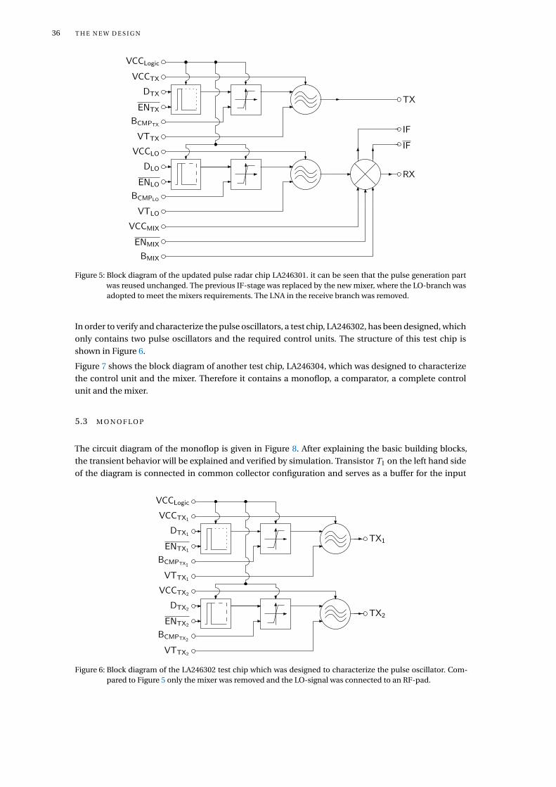
In order to verify and characterize the pulse oscillators, a test chip, LA246302, has been designed, which
only contains two pulse oscillators and the required control units. The structure of this test chip is
shown in Figure 6.
Figure 7 shows the block diagram of another test chip, LA246304, which was designed to characterize
the control unit and the mixer. Therefore it contains a monoflop, a comparator, a complete control
unit and the mixer.
5.3 M O N O F L O P
The circuit diagram of the monoflop is given in Figure 8. After explaining the basic building blocks,
the transient behavior will be explained and verified by simulation. Transistor T1 on the left hand side
of the diagram is connected in common collector configuration and serves as a buffer for the input
DTX1
ENTX1
DTX2
ENTX2
TX2
TX1
VCCLogic
VCCTX1
BCMPTX1
VTTX1
BCMPTX2
VTTX2
VCCTX2
Figure 6: Block diagram of the LA246302 test chip which was designed to characterize the pulse oscillator. Com-pared to Figure 5 only the mixer was removed and the LO-signal was connected to an RF-pad.

5.3 M O N O F L O P 37
D
EN
D
EN
VCC
BCMP
D
BCMP
LO
ENMIX
VCC
BMIX
IF
IF
VCC
VCC
RF
Q
Q
Q
Figure 7: Block diagram of the LA246304 test chip which was designed to characterize the digital components andthe mixer. It can be seen, that each part of the control unit, as well as the complete control unit, are fullyaccessible. Also the new mixer is contained in the chip.
signal. The transistor of the next stage, T2, is connected in common emitter configuration and builds
an inverter. The next stage is a switchable current mirror. T4 and T5 are connected as current mirror
and T3 is used as a switch. If T3 is on, it ties the base of T4 and T5 to ground and the current mirror is
off. Otherwise, the voltage level at the EN input defines the current that is mirrored into R12 and so the
maximum output voltage can be programmed. T6 builds another inverter at whose output the signal Q
is measured. T7 serves as a buffer to decouple the output TST, which can be used for measurements of
the monoflop. The capacitor C1 defines the time constant of the circuit. It is implemented as a main ca-
pacitor which is connected in parallel by fuses with 3 smaller capacitors. The main capacitor is 1.05pF
and the smaller capacitors are 0.525pF each. R11 and R12 have a value of 1.25kΩ each. This offers the
possibility to modify the minimum pulse width, which can be generated by the monoflop.
The circuit is in its default state, when either no signal is connected to the input D, or 0V is applied to
it. In this state, T1 and T2 are off. The output of the first inverter T2 is high and the current mirror is off,
resulting in a high output voltage at the collector of T5. Hence, T6 is on and its output voltage is low.
The voltage drop across the capacitor is zero and the feedback path over R10 secures this state. With
the rising edge of the input signal, T1 turns on. Because R4 has a lower resistance than R10, T2 turns
on, which activates the current mirror and ties the left connection of C1 to ground. At first glance, the
voltage drop across C1 remains zero what turns off T6 and the voltage at the Q output is high. Now C1 is
charged via R12, where the charging curve depends on the voltage programmed with the EN input and
thus the current of the current mirror, and the voltage at the base of T6 increases. When the voltage
reaches the switching threshold of T6, it turns on and the output voltage of the monoflop is low again.
When the control input D goes back to zero later the circuit is in its default state again.
In order to verify and characterize the monoflop, a transient simulation was made. Therefore the
monoflop was connected to a 1.8V supply voltage and no load was connected to its output. To pro-
vide an input signal, a pulse voltage source was used. It was configured to produce rectangular shaped
pulses with a pulse width of 80ns and a period of 100ns. For the rise time and the fall time of the edges,
a time of 1ns was chosen. The lower voltage level was set to 0V, the upper level to 3.3V. Transient simu-
lations were made for different configurations of the fuses R0, R1 and R2, and different settings for the
EN voltage. The output signal of the monoflop was captured and the pulse width was evaluated using

38 T H E N E W D E S I G N
R1
R2
D
T1
R3
R4 R5T2
R6T3 T4 T5
R7
EN
T6
R8
R9
T7
R10
C1
R11 R12 R13
R14
Q
TST
Figure 8: Circuit diagram of the monoflop. The minimum pulse width is defined by the capacitor C1. C1 is realizedas 4 capacitors which are connected in parallel using laser fuses. Thus the minimum pulse width can bechanged with the fuses. The pulse width can be extended with the voltage level at the VEN input.
MATLAB . The simulation results are shown in Figure 9. The simulation results fit to the expectations.
The jitter introduced by the monoflop was simulated using a pss-simulation and a pnoise-simulation.
The simulation has shown that the cycle-to-cycle-jitter, JCC , is 108.5fs which is less than 1% of the
oscillators period.
5.4 C O M PA R AT O R
The comparator is implemented as a differential amplifier without any feedback as shown in the circuit
diagram in Figure 10. The core of the differential amplifier is composed of T1, T2, R1, R2 and R3, where
the latter serves as tail current source. At the non-inverting input, the input signal D is connected via
R7. R6 has a high resistance and provides a connection to ground if the input is not connected. At
the inverting input, a bias voltage, which programs the comparators switching threshold voltage, is
applied. The bias voltage is generated from the supply voltage by the resistive voltage divider R4 and
R5. The bias input allows external tuning of the bias voltage.
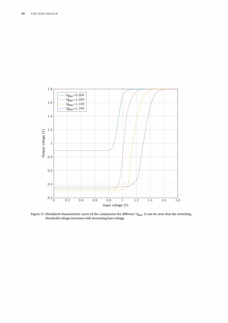
The characteristic curve of the comparator was simulated using a swept DC simulation, where the
input voltage was swept. The simulation was done for different settings of the VBias voltage. The com-
parator was supplied with 1.8V and had no load connected to it. The resulting characteristic curves,
shown in Figure 11, lead to the conclusion, that the comparator works as expected.
To verify the comparator’s dynamic behavior and to evaluate the influence of the comparator on the
control signal, the cascade of monoflop and comparator was simulated, similar as it is described in
Section 5.3. In Figure 12, the simulated pulse width is plotted over VEN for different VBias voltages. It
can be seen that the pulse width changes with the VBias voltages. This is caused by the finite slew rate
of the signal produced by the monoflop. As VBias increases, the pulse width becomes shorter.
The jitter generated by the cascade of monoflop and comparator was also simulated. Depending on
the VBias setting, the result fluctuates around 115fs, which is still a good value. The jitter simulation
was done in the same way as described in Section 5.3.

5.4 C O M PA R AT O R 39
0 0.2 0.4 0.6 0.8 1 1.2 1.41
2
3
4
5
6
7
8
9
10
VEN (V)
Pulse
widt
h(n
s)
R0R1R2none
Figure 9: Simulated pulse width vs. VEN for all meaningful fuse configurations. It can be seen that a pulse widthfrom 1.5ns up to infinity can be achieved. The minimum pulse width depends on the fuse setting.
R1 R2
R3
R4
R5
R6
R7
R8T1 T2
T3
D Bias
Q
Figure 10: Circuit diagram of the comparator. The comparator is realized as a free running differential amplifier,which consists of the transistors T1 and T2. At the base of T2, a reference voltage is applied. When theinput voltage is higher than the reference voltage, the output switches to a high voltage level.
40 T H E N E W D E S I G N
0 0.2 0.4 0.6 0.8 1 1.2 1.4 1.6 1.80.2
0.4
0.6
0.8
1
1.2
1.4
1.6
1.8
Input voltage (V)
Out
putv
olta
ge(V
)
VBias=0.90VVBias=1.00VVBias=1.10VVBias=1.20V
Figure 11: Simulated characteristic curve of the comparator for different VBias. It can be seen that the switchingthreshold voltage increases with increasing bias voltage.

5.4 C O M PA R AT O R 41
0 0.2 0.4 0.6 0.8 1 1.2 1.42
3
4
5
6
7
8
9
10
VEN (V)
Pulse
widt
h(n
s)
VBias=0.90VVBias=1.00VVBias=1.10VVBias=1.20V
Figure 12: Simulated pulse width after the comparator vs. VEN for different VBias. It can be seen that the minimumpulse width is higher than that one of the single monoflop (see Figure 10).

42 T H E N E W D E S I G N
5.5 P U L S E O S C I L L AT O R
The requirements on the pulse oscillator in order for the pulse radar to work, were already explained
in subsection 4.2.4. A circuit diagram of the pulse oscillator is shown in Figure 13. It consists of the
driver stage on the left side of the diagram and the Colpitts oscillator on the right side. The two parts
are linked via the oscillators tail current source, which is the current mirror composed of T4, T5 and R6
in the center of the diagram. The transmission line T L3 acts as a RF choke, such that only a DC current
can pass, for the RF current, it is a high impedance. The resistive voltage divider R2 and R3 allows to
set the operating point of the oscillators amplifying transistor T1. C5 provides a path to ground for the
RF signal. The tank circuit, which defines the oscillation frequency, consists of C1 and C2 together with
the inductance of the transmission line T L2. In order to make the oscillation frequency tunable, C2 is
connected in parallel with the tunable capacitor built by C3, C4 and T3. The tunable capacitor uses the
dependence of the junction capacitance of transistor T3 on the bias voltage to change its capacitance.
Thus the VT input can be used to adjust the oscillation frequency. Usually, varactors are used in reverse
bias configuration for this purpose. When the tuning voltage increases, the junction capacitance of
the varactor decreases and the oscillation frequency increases. In the approach which was used in this
work, the transistor T3 works like a varactor in forward direction and thus the oscillation frequency
decreases with increasing tuning voltage. The cascode stage T2 provides some gain and serves as a
buffer between the oscillator and the load.
On the left side of the current mirror, the reference current is produced by the driver stage. The wire
which connects the driver stage and the current mirror has a very low width and thus implements the
inductor L1. L1 serves as an RF block. If the control signal D is 0V, T6 and T8 are off, T9 and T7 are
on. The latter ties the output of the driver stage to ground and hence no tail current is provided to
the oscillator. When the voltage of the control signal rises, T8 and the inverter built from T6 turns on.
The output voltage of T6 goes low and T7 as well as T9 are switched off. The reference current for the
current mirror is now defined by R10,R7 and T8. Consequently, the oscillator goes on. The slew rate
of the input signal defines the time between the rising edge of the control signal and the start of the
oscillation. Hence, the coherence of the oscillator can be influenced with the control signal.
The characterization of the oscillator starts with the evaluation of its CW performance in terms of out-
put power and frequency tuning range. To obtain the output power and the oscillation frequency, a
pss-simulation was made. The oscillator and the required control unit consisting of the monoflop and
the comparator are included in the simulation. To configure the oscillator for CW operation, a constant
voltage of 3.3V was connected to the D input and the EN input was connected to 1.8V. The supply volt-
age of the oscillator was swept and to ensure that the oscillator will start in simulation, the initial volt-
age across C2 was set to 100µV. First the output power was captured when the tuning voltage was 0V.
In order to calculate the oscillator’s DC-to-RF conversion gain, also the DC input current was captured.
The results for the output power are shown in Figure 14. In Figure 15, the calculated conversion gain
is shown. As next step the tuning range was analyzed. Therefore the tuning voltage was swept and the
oscillation frequency was captured. In Figure 16, the dependence of the oscillation frequency on the
VTune voltage is shown for different settings of the supply voltage. When the tuning voltage is increased,
starting from 0V, first the oscillation frequency does not change significantly. When the typical diode
threshold voltage is reached, the junction capacitance begins to change and hence the oscillation fre-
quency also changes. When the voltage is further increased, the tuning sensitivity decreases. Finally,
the tuning range is calculated by subtracting the minimum oscillation frequency from its maximum.
The result for different values of VOsc is shown in Figure 17.
As a next step, the oscillator’s pulse performance was simulated. For that, the EN input of the control
unit was set to 0V and a rectangular signal with a magnitude of 3.3V and a period of 200ns was applied
at the D input. All fuses are closed and both the oscillator and the control unit are supplied with 1.8V. A
transient simulation is made and the output voltage of the oscillator is captured. Because the first pulse
of the oscillator differs from the others, the second pulse which is shown in Figure 18, is used to extract
its envelope and to compute the envelope’s autocorrelation function. The normalized envelope of the

5.5 P U L S E O S C I L L AT O R 43
T1
C1
C2 C3
C4
T3
R4
R5
T L2
R2C5
R3
T L3
R6
T5 T4
T2
T L1
C6
Q
VT
R7R8
T8
L1
T6
R9
T9
R10
T7
R11
R12
R13
D
Figure 13: Circuit diagram of the pulse oscillator. The pulse oscillator consists out of a singled ended Colpitts os-cillator and a driver stage.

44 T H E N E W D E S I G N
1.6 1.8 2 2.2 2.4 2.6 2.8 3−20
−15
−10
−5
0
5
10
VOsc (V)
Out
putp
ower
(dB
m)
VTune=0.00V
Figure 14: Simulated output power vs. VOsc. At the nominal supply voltage of 1.8V, the oscillator shows an outputpower of approximately 2dBm.

5.5 P U L S E O S C I L L AT O R 45
1.6 1.8 2 2.2 2.4 2.6 2.8 3−30
−28
−26
−24
−22
−20
−18
−16
−14
−12
−10
VOsc (V)
Conv
ersio
nga
in(d
B)
VTune=0.00V
Figure 15: Simulated conversion gain of the oscillator vs. VOsc. The conversion gain is the quotient of RF outputpower and the DC input power. It can be seen that the conversion gain is between−10dB and−12V.

46 T H E N E W D E S I G N
0 0.2 0.4 0.6 0.8 1 1.2 1.4 1.6 1.877.5
78
78.5
79
79.5
80
80.5
VTune (V)
Peak
frequ
ency
(GH
z)
VOsc=1.80VVOsc=1.90VVOsc=2.00VVOsc=2.10VVOsc=2.20VVOsc=2.30VVOsc=2.40V
Figure 16: Simulated output frequency vs. VTune for different settings of VOsc. It can be seen, that width increas-ing tuning voltage, the frequency decreases. It can also be seen, that the oscillation frequency is moresensitive to the supply voltage than to the tuning voltage.

5.5 P U L S E O S C I L L AT O R 47
1.8 1.85 1.9 1.95 2 2.05 2.1 2.15 2.2 2.25 2.3 2.35 2.40.3
0.4
0.5
0.6
0.7
0.8
0.9
VOsc (V)
Tuni
ngra
nge
(GH
z)
Figure 17: Simulated tuning range vs. VOsc. It can be seen that the tuning range is close to 900MHz for the desiredoperating conditions.

48 T H E N E W D E S I G N
201 201.5 202 202.5 203 203.5 204 204.5 205 205.5 206−500
−400
−300
−200
−100
0
100
200
300
400
500
Time (ns)
Mag
nitu
de(m
V)
Figure 18: Simulated transient pulse. The shape of the envelope is almost rectangular with a small overshootingin the beginning and at the end of the pulse.
pulse, is very close to a rectangular shape. Consequently, the autocorrelation function has an almost
triangular shape.
5.6 M I X E R
As explained in Section 5.1, the mixer published in [9] perfectly satisfies all the requirements that are
necessary for the pulse radar. A drawback is, that this mixer requires the LO and RF signals to be differ-
ential signals. Because of the used rat-race coupler, the mixer occupies much area on the chip. Thus it
was decided to design a single-ended version of the mixer. Similar to [9], the design was started with a
singled balanced mixer with two diodes and a rat race coupler. The schematic diagram of such a mixer
is shown in Figure 19. The rat race coupler on the left hand side of the diagram produces the signal
(LO+RF) at the Σ output, where at the ∆ output, the signal (−LO+RF) occurs. The output voltages
of the rat race coupler are applied to the diodes D1 and D2. Usually Shottky diodes are used, because
the power of the LO signal must be high enough to switch the diodes and Shottky diodes typically have
a lower barrier potential compared to pn-junction diodes. Because of the exponential characteristic
curve of the diodes, the current flowing through the diodes contains a portion which is proportional
to the product of the LO signal and the RF signal. This product can be further decomposed into a sig-
nal with the sum frequency and a signal with the difference frequency. The capacitor C1 provides a
path to ground for the high frequency components of the current, where for the difference frequency,
which is much lower than all the other components, the capacitor has a high impedance. Thus the
difference frequency appears at the IF output. If there is no LO signal present at the input, the diodes
are not forward biased and hence the current flowing through them is close to zero. In this case, the
output resistance of the mixer is very large. In combination with the load capacitor, a lossy integrator

5.6 M I X E R 49
90
90
90
270
LO
RF
Σ= RF+LO
∆= RF−LO
D1
D2
C1
IF
Figure 19: Schematic diagram of a single balanced diode mixer. A rat-race coupler is used to generate the sum Σ
and the difference ∆ signal. The non-linearity of the diodes is the used to perform the multiplication.The required RF ground is provided with the capacitor C1.
is formed, whose time constant is very large. Therefore the lossy integrator is a very good approxima-
tion of an ideal one, as it is required by the signal model (refer to chapter 2 for more details). However,
in the used technology (see chapter 3), neither diodes nor Shottky diodes are available. Nevertheless,
every bipolar transistor is made from two pn-junctions. A diode can be realized, when connecting e.g.
the base and the collector pin of a bipolar transistor. This shortens the base-collector-junction and the
diode is the remaining base-emitter-junction. Unfortunately, the barrier potential of such a diode is
very high and in combination with the oscillator described in Section 5.5, the mixer cannot be oper-
ated. To overcome this issue, a small bias current must be applied, similar as described in [9].
A simulation of the single-balanced mixer has shown, that a DC-offset appears at the IF-output. It is
obvious that the bias current of the diodes has shifted their operating point away from zero, what con-
tributes to the offset. This effect could be taken into account by subtracting the DC-operating point
from the output signal. Further simulations without RF signal have shown that there is still a large off-
set remaining which depends on the power of the LO signal. This offset has its origin in the rectification
effect of the diodes and in the resistive coating of the transmission lines. The latter leads to an inequal-
ity in the power present at the Σ output and the power present at the ∆ output of the rat race coupler.
Consequently, the undesired rectification components of the diode currents do not cancel each other
anymore. The offset is incompatible with the function of the pulse radar. Figure 20 shows the funda-
mental idea of how the offset can be compensated. On the right hand side of the diagram, a second
diode branch was added. The direction of the new diodes is swapped compared with the direction of
the old ones. A simulation has shown, that the offset in both output signals is nearly equal and hence
nearly vanishes in the differential output signal, measured across IF and IF.
In Figure 21, the circuit diagram of the complete designed mixer is shown.
The design of the mixer started with the rat race coupler, which is shown on the left hand side of the
circuit diagram. Because of the length of the transmission lines and the limited chip area, the design
was not straight forward. Several bends had to be made and the effect of the bends onto the effective
length of the transmission line was taken into account in the simulation model. According to [10], a rat
race coupler has an impedance of ZIn = Z0p2
at its ports, where Z0 is the impedance of the transmission
line used to build the coupler. To achieve an input impedance of 50Ω, out of the impedances, which
are available in the technology, a 70Ω transmission line was selected to realize the rat race coupler. The
simulated port matching of the designed rat race coupler is shown in Figure 22, Figure 23 shows the
simulated isolation between LO and RF port.
The next step was the implementation of the diodes and their bias circuit. The diodes are implemented
using the diode connected transistors T1, T2, T3 and T4. The transmission lines T L7, T L8, T L9 and
T L10 have been included to account for the effects of the interconnection between the diodes in the

50 T H E N E W D E S I G N
90
90
90
270
LO
RF
Σ
∆
D1
D2
C1
IF
D3
D4
C2
IF
Figure 20: Schematic diagram of the designed mixer. Compared to Figure 19, a second diode branch was added tocompensate the DC-offset voltage.
simulation. T L5, T L6, T L11 and T L12 serve as RF-chokes and as matching elements. The bias circuit
consists of the current mirror T5 and T7 where the diode connected transistors T8 and T9 serve as a
level shifter. The mirror current is set by the resistor R1. It can be tuned with the voltage applied at
the bias input. The bias voltage of the diodes is stabilized with the capacitor C1 which also serves as a
path to ground for the RF chokes. With T6, a switch is implemented which can be used to turn the bias
current off, which increases the output impedance of the mixer when the mixer is not needed. T6 is
critical in terms of its break down voltage, but its use can be tolerated in an experimental circuit. When
a voltage of 1.8V is applied to the EN input, the mixer is off, a voltage of 0V turns the mixer on.
The final step in the design of the mixer was to mate the rat race coupler with the diodes. Therefore
the input impedance of the diode network was simulated and a matching network was designed. It is
clear that the input impedance of the diode network depends on the applied LO power. The rat-race
coupler splits the LO power up into two branches, where in each branch the power is split up again
for each diode branch. A psp-simulation was made on top of a pss-simulation with meaningful power
settings.
The matching network, which consists of T L1, T L3, C1 and C3, was designed based on the data ob-
tained from the simulation. In the first step, the coupling capacitor and the effect of the cross connec-
tion of the inputs were simulated. In the next step, the impedance of the cross connected diodes was
matched to 50Ω. Figure 24 shows the achieved scattering parameters, where the same simulations like
for the input impedances have been used.
Finally, the matching and isolation of the whole mixer was simulated. Figure 25 shows the matching of
the mixer, which is very good in the frequency range of interest. In Figure 26, the simulated isolation
between the mixers LO and RF input is shown. Also for the isolation, a good result has been achieved.
Now as the design of the mixer is finished, the performance of the mixer is evaluated in simulation.
First, the voltage conversion gain of the mixer is simulated. Comparable to [9], the mixer has a voltage
conversion gain slightly below 0dB. The simulation results can be seen in Figure 27 and Figure 28. For
the IF signal frequency, a value of 10MHz was chosen and the mixer was loaded with a capacitor of
10pF.
Also, the effect of the EN input on the voltage conversion gain was simulated. Figure 29 shows that the
voltage conversion gain of the mixer decreases dramatically when the voltage at the EN input exceeds
1.1V.
In order to calculate the SNR at the output of the system, the noise figure (Figure 30) and the output
noise (Figure 31) of the mixer is simulated. To get the effective value of the output noise voltage, the
output noise is integrated in a bandwidth of 1MHz. Slightly fluctuating with the LO power, this results
in approximately 2µV.
To integrate the mixer into the signal model from chapter 2, the mixer’s functionality is approximated

5.6 M I X E R 51
T L5 T L6
C3
P C5
N
T1 T2
T L7 T L8
T L9 T L10
T3 T4
T L11 T L12
C4
P
C6
N
IF IF
C1
2T5
T6
R3
EN
R4
T7
T8
T9
R1R2
Bias
T L1
T L2
C1
C2
T L3
T L4
90
90
90
270
LO
RF
Σ
∆
Figure 21: Circuit diagram of the designed mixer. It consists of the rat race coupler shown on the left, the two diodebranches in the middle and the bias current mirror on the top right side of the diagram.

52 T H E N E W D E S I G N
20 30 40 50 60 70 80 90 100 110 120 130 140−50
−45
−40
−35
−30
−25
−20
−15
−10
−5
0
Frequency (GHz)
|Si,
i|(d
B)
S11, S44
S22, S33
Figure 22: Simulated matching of the rat race coupler. It can be seen that a matching of−20dB or better is achievedin a bandwidth of 20GHz around the design frequency.

5.6 M I X E R 53
20 30 40 50 60 70 80 90 100 110 120 130 1405
10
15
20
25
30
35
Frequency (GHz)
|S1,
2|(
dB
)
Figure 23: Simulated LO-RF isolation of the rat race coupler. It can be seen that an isolation closes to 35dB isachieved at the design frequency.
54 T H E N E W D E S I G N
50 55 60 65 70 75 80 85 90 95 100−35
−30
−25
−20
−15
−10
−5
0
Frequency (GHz)
|Si,
i|(d
B)
S11,P=−3dBmS22,P=−3dBmS11,P=−1dBmS22,P=−1dBm
Figure 24: Simulated matching of the rectifier. it can be seen, that the matching is better than 15dB in a bandwidthof 5GHz. Because of the non-linearity of the diodes, the input impedance depends on the used power.
5.6 M I X E R 55
50 55 60 65 70 75 80 85 90 95 100−45
−40
−35
−30
−25
−20
−15
−10
−5
0
Frequency (GHz)
|Si,
i|(d
B)
S11,PLO=0dBmS22,PLO=0dBmS11,PLO=2dBmS22,PLO=2dBm
Figure 25: Simulated matching of the whole mixer. At the design frequency, a matching between −30dB and−40dB is achieved.

56 T H E N E W D E S I G N
50 55 60 65 70 75 80 85 90 95 10010
15
20
25
30
35
40
Frequency (GHz)
|Si,
j|(d
B)
S1,2,PLO=0dBmS1,2,PLO=2dBm
Figure 26: Simulated LO-RF isolation of the whole mixer. It can be seen that the isolation at the design frequencyis close to 40dB

5.6 M I X E R 57
−5 −4 −3 −2 −1 0 1 2 3 4 5−12
−10
−8
−6
−4
−2
0
PLO (dBm)
Conv
ersio
nga
in(d
B)
PRF=−40dBmPRF=−18dBmPRF=5dBm
Figure 27: Simulated voltage conversion gain vs. LO power. When the RF power is small, the mixer shows a con-version gain close to 0dB. When the RF power is too high, the mixers saturates and the conversiondecreases.

58 T H E N E W D E S I G N
−40 −35 −30 −25 −20 −15 −10 −5 0 5−12
−10
−8
−6
−4
−2
0
PRF (dBm)
Conv
ersio
nga
in(d
B)
PLO=−5dBmPLO=−1dBmPLO=5dBm
Figure 28: Simulated voltage conversion gain vs. RF power. It can be seen that the mixer reaches it’s 1dB-compression point when the RF power is approximatly −7dB. With increasing LO power, the compres-sion point moves to the right.

5.6 M I X E R 59
0 0.2 0.4 0.6 0.8 1 1.2 1.4 1.6 1.8 2−120
−100
−80
−60
−40
−20
0
VEN (V)
Conv
ersio
nga
in(d
B)
PLO=−5dBm, PRF=−40dBmPLO=0dBm, PRF=−40dBmPLO=5dBm, PRF=−40dBm
Figure 29: Simulated voltage conversion gain vs. VEN. It can be seen that the voltage conversion gain decreaseswhen the mixer is turned off.

60 T H E N E W D E S I G N
0 1 2 3 4 5 6 7 8 9 1012
12.2
12.4
12.6
12.8
13
13.2
Frequency (MHz)
Noise
figur
e(d
B)
PLO=−5dBmPLO=0dBmPLO=5dBm
Figure 30: Simulated noise figure. It can be seen that the noise figure is between 12dB and 13dB.
with the model shown in Figure 32. In this model, the input voltages URF and ULO on the left side repre-
sent the magnitudes of the corresponding input voltages of the real mixer. The behavior of each of the
two diode branches is modeled in a small signal approximation with two voltage controlled current
sources, which have the transconductances g mRF,j and g mLO,j, where the first one is responsible for
the conversion gain and the second one takes into account for the DC-offset resulting from the rectifi-
cation of the LO signal. The output resistance is modeled with the resistor Ri,j and the increase of the
output impedance due to disabling the mixer is included with the switch and REN,j. The switches are
closed when the mixer is on. The load capacitors 2CL are the sum of the internal RF-ground capacitor
and any external connected capacitive load.
To make the extraction of the parameters easier, the differential model is transformed into the model
shown in Figure 33. The meaning of the components remain the same
In order to extract the LO transconductance g mLO, a pac-simulation was made where the mixers out-
put was connected to a high capacitance and the differential current flowing through the mixer ter-
minals was captured. Dividing the current by the LO voltage delivers the LO transconductance. In
Figure 34, the result is plotted over VBias for different LO power settings. In Figure 35, the extracted LO
transconductance is plotted over the VEN voltage. It can be seen that it goes to zero, when the mixer is
off.
A similar method has been used to extract the RF transconductance g mRF. In Figure 36, the extracted
RF transconductance is shown over VBias. In Figure 37, the course of the transconductance with respect
to VEN is shown. It can be seen that the RF-transconductance goes to zero when the mixer is switched
off. Compared to the LO transconductance, the RF transconductance is much higher.
To extract the output impedance of the mixer, the mixer was connected to a sp-simulation port and a
psp-simulation was done. The simulated output resistance with respect to VBias, when the mixer is on,

5.6 M I X E R 61
0 1 2 3 4 5 6 7 8 9 101.4
1.45
1.5
1.55
1.6
1.65
1.7
1.75
1.8
1.85
Frequency (MHz)
Out
putn
oise
(n
V√
Hz)
PLO=−5dBmPLO=0dBmPLO=5dBm
Figure 31: Simulated output noise. The output noise of the mixer is used later to estimate the SNR of the pulseradar.
RF
RRF
URF
LO
RLO
ULO
g mLO,1 g mRF,1
Ri,1
REN,1
2CL
IF IFUIF
g mLO,2g mRF,2
Ri,2
REN,2
2CL
E N E N
Figure 32: Modell of the mixer. Each diode branch is modelled with a current source for the conversion gain andan additional current source to take the DC-offset into account. The dependence of the mixers outputimpedance on the VEN voltage is taken into account with the switches.
62 T H E N E W D E S I G N
RF
Rin,RF
URF
LO
Rin,LO
ULO
g mLO g mRF
Ri
REN
IIF
CL
IF
IF
UIF
E N
Figure 33: Transformed model of the mixer. The two branches from Figure 32 are combined, but the output voltageis still differential. This model is used to calculate the output signal of the designed pulse radar.
1.5 1.6 1.7 1.8 1.9 2 2.1 2.2 2.30
100
200
300
400
500
600
700
800
VBias (V)
gm
LO(µ
S)
PLO=−2dBmPLO=0dBmPLO=2dBm
Figure 34: Simulated LO transconductance of the mixer. The LO transconductance relates the mixers IF outputcurrent to the applied LO magnitude. It can be used to approximate the DC-offset voltage at the outputof the pulse radar.

5.6 M I X E R 63
0 0.2 0.4 0.6 0.8 1 1.2 1.4 1.6 1.8 20
100
200
300
400
500
600
700
800
VEN (V)
gm
LO(µ
S)
PLO=−2dBm, VBias=1.50VPLO=−2dBm, VBias=1.85VPLO=−2dBm, VBias=2.20VPLO=0dBm, VBias=1.50VPLO=0dBm, VBias=1.85VPLO=0dBm, VBias=2.20VPLO=2dBm, VBias=1.50VPLO=2dBm, VBias=1.85VPLO=2dBm, VBias=2.20V
Figure 35: Simulated LO transconductance of the mixer vs. VEN. It can be seen that the LO transconductance goesto zero when the mixer is turned off.

64 T H E N E W D E S I G N
1.5 1.6 1.7 1.8 1.9 2 2.1 2.2 2.30
2
4
6
8
10
12
14
VBias (V)
gm
RF
(mS)
PLO=−2dBmPLO=0dBmPLO=2dBm
Figure 36: Simulated RF transconductance of the mixer. The RF transconductances relates the mixers IF outputcurrent to the magnitude of the RF input voltage.

5.6 M I X E R 65
0 0.2 0.4 0.6 0.8 1 1.2 1.4 1.6 1.8 20
2
4
6
8
10
12
14
VEN (V)
gm
RF
(mS)
PLO=−2dBm, VBias=1.50VPLO=−2dBm, VBias=1.85VPLO=−2dBm, VBias=2.20VPLO=0dBm, VBias=1.50VPLO=0dBm, VBias=1.85VPLO=0dBm, VBias=2.20VPLO=2dBm, VBias=1.50VPLO=2dBm, VBias=1.85VPLO=2dBm, VBias=2.20V
Figure 37: Simulated RF transconductance of the mixer vs. VEN. It can be seen that the RF transconductance ismuch higher than the LO transconductance.

66 T H E N E W D E S I G N
1.5 1.6 1.7 1.8 1.9 2 2.1 2.2 2.310−1
100
101
102
103
104
VBias (V)
|ZO
ut|
(kΩ
)
Figure 38: Simulated output impedance of the mixer when it is enabled. With increasing bias voltage, the outputimpedance decreases because the operating point of the mixer diodes is shifted towards the conductingregion.
is shown in Figure 38. In Figure 39, the course of the output impedance over VEN is shown. It can be
seen that the output impedance of the mixer decreases with increasing bias current, but dramatically
increases when the mixer is turned off. The simulation results show that the mixer works.

5.6 M I X E R 67
0 0.2 0.4 0.6 0.8 1 1.2 1.4 1.6 1.8 20
5
10
15
20
25
30
35
40
45
VEN (V)
|ZO
ut|
(MΩ
)
VBias=1.50VVBias=1.85VVBias=2.20V
Figure 39: Simulated output impedance of the mixer vs. VEN. It can be seen that the output impedance increasesdramatically when the mixer is turned off. Thus the integrating capacitor is prevented from dischargingwhich increases the magnitude of the pulse radar’s output signal.

68 T H E N E W D E S I G N
5.7 L I N K B U D G E T A N A LY S I S
In this section, the performance of the pulse radar system in terms of the magnitude and SNR of the
output signal is calculated based on the results of the simulations. As a first step, the output current of
the mixer is calculated using the signals defined in chapter 2
IIF (t ) = g mRFsRX (t ) sLO (t )+ ALOg mLOsLO (t ) . (55)
Where ALO is the magnitude of the LO signal in V. Inserting in the signals and simplifying as done in
chapter 2 results in
IIF (t ) = A0αRTg mRF
kmax∑k=−kmax
p (t −kTLO) p (t −kTLO −k∆T )+
ALOg mLO
kmax∑n=−kmax
h (t −nTLO) . (56)
Inserting the pulse functions yields
IIF (t ) = A0αRTg mRF
2
kmax∑k=−kmax
cos(ω0k∆T )h (t −kTLO)×
×h (t −kTLO −k∆T )rect
(t −kTLO −k ∆T
2
Tp −|k|∆T
)+ ALOg mLO
kmax∑n=−kmax
e (t −nTLO) . (57)
The first term on the right hand side is similar to the result from the signal model, the second term is a
disturbance term which comes from the rectification of the LO signal in the mixer. The current is now
used as an input for an RC-low pass filter, consisting of the mixers output impedance and an external
capacitor as shown in Figure 40.
In Time Domain, the RC-Network is described with the following differential Equation
IIF (t ) = 1
RIUIF (t )+CL
dUIF (t )
dt. (58)
The Equation is now integrated over time on both sides and divided by CL
1
CL
t∫−∞
IIF(t ′
)dt ′ = 1
RICL
t∫−∞
UIF(t ′
)dt ′+UIF (t ) . (59)
IIF (t )
RI CL UIF (t )
Figure 40: RC-network used to model the behavior of the mixers output impedance in combination with the ex-ternal load capacitor.
5.7 L I N K B U D G E T A N A LY S I S 69
Now the output current (58) from the mixer is inserted into (59), only the left hand term of the integro-
differential equation is viewed. This term represents the input signal of the described system
t∫−∞
A0αRTg mRF
2CL
kmax∑k=−kmax
cos(ω0k∆T )h(t ′−kTLO
)h
(t ′−kTLO −k∆T
)rect
(t ′−kTLO −k ∆T
2
Tp −|k|∆T
)+ ALOg mLO
CL
kmax∑n=−kmax
e(t ′−nTLO
)dt ′. (60)
As a next step, the integral is split and the left hand term is processed as it was done in chapter 2. In the
right hand term, the sum and the integral are exchanged and furthermore, the sum can be replaced
by (n +kmax), because the summand does not depend on n. Sampling at t = nTLO gives the following
equation for the input signal of the system
x (nTLO) = A0αRTg mRFφee (0)
2CL
n∑k=−kmax
cos(ω0k∆T )ree (k∆T )+
ALOg mLO
CL(n +kmax)
∞∫−∞
e (t )dt . (61)
(61) can be approximated using the Heaviside function. Additionally, the function has been shifted in
time to meet the requirements of the later applied Laplace transformation
x (t ) =n∑
k=0∆x (k −kmax)Θ (t −kTLO) . (62)
Where the difference between two consecutive steps ∆x[n] is given as
∆x [n] = A0αRTg mRFφee (0)
2CLcos(ω0n∆T )ree (n∆T )+ ALOg mLO
CL
∞∫−∞
e (t )d t . (63)
and
n =⌊
t
TLO
⌋. (64)
The Laplace transform of this signal can be calculated using the linearity of the Laplace transform and
the Laplace transform of the Heaviside function combined with the time shift property found in [4]
X (s) =n∑
k=0∆x [k −kmax]
1
se−kTLOs . (65)
In order to compute the output signal, the transfer function of system is needed. It can be easily calcu-
lated using the Laplace transform
H (s) = s1
τRC+ s
. (66)
where the time constant τRC is given by
τRC = 1
RICL. (67)

70 T H E N E W D E S I G N
The output signal of the pulse radar can then be calculated
UIF (s) = X (s)H(s). (68)
UIF (s) =n∑
k=0
s1
τRC+ s
∆x (k −kmax)1
se−kTLOs . (69)
UIF (s) =n∑
k=0
11
τRC+ s
∆x (k −kmax)e−kTLOs . (70)
Inverse transform into time domain and reversing the time shift gives
UIF (t ) =n∑
k=−kmax
e− t−(k+kmax)TLO
τRC ∆x [k] . (71)
Inserting the signals from above
UIF (t ) = A0αRTg mRFφee (0)
2CL
n∑k=−kmax
e− t−(k+kmax)TLO
τRC cos(ω0k∆T )ree (k∆T )
+ ALOg mLO
CL
∞∫−∞
e (t )dtn∑
k=−kmax
e− t−(k+kmax)TLO
τRC . (72)
Each of the summands represent a convolution of a signal with the impulse response of the RC-network.
The input signal for the second sum is a constant. Because of this, the second sum describes the charg-
ing curve of the RC-network which saturates after several pulses and can then be removed easily with
a filter. The first term corresponds to the result from the Section 2.1, extended with the lossy integrator.
Therefore the mixer gain factor can be extracted
αM = g mRF
CL. (73)
In the same manner as in Section 2.1, the transfer function is computed by applying the Laplace trans-
form
H (s) = 1
s + TLOτRC
. (74)
The frequency response is then
|H (iω)| = 1√ω2 + T 2
LO
τ2RC
. (75)
argH (iω) =−arctanωτRC
TLO. (76)
It is used to approximate the magnitude of the output signal as it is done in Section 2.3. In combination
with the simulated output noise of the mixer, the SNR at the output of the pulse radar can be approx-
imated. For that purpose, it is assumed that the VCO operates at a frequency of 79GHz and delivers
a power of 0dBm. The speed of light is assumed to be c = 3 ·108 ms and the output impedance of the
mixer is 20kΩ. The simulated envelope of the VCO is used for calculation.
In Figure 41, the magnitude of the maximum of the output pulse is plotted over the difference ∆ f
between LO and RX pulse rate for certain fixed LO pulse rates fLO. For the load capacitance CL a value
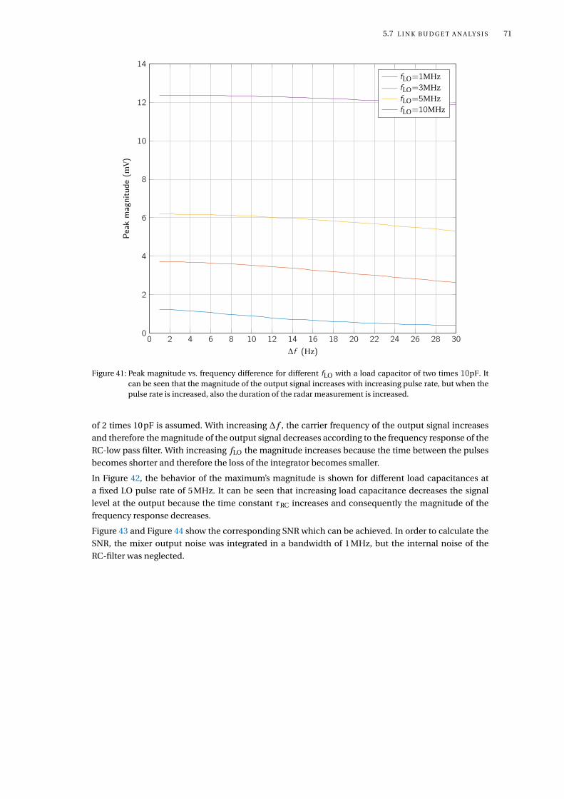
5.7 L I N K B U D G E T A N A LY S I S 71
0 2 4 6 8 10 12 14 16 18 20 22 24 26 28 300
2
4
6
8
10
12
14
∆f (Hz)
Peak
mag
nitu
de(m
V)
fLO=1MHzfLO=3MHzfLO=5MHzfLO=10MHz
Figure 41: Peak magnitude vs. frequency difference for different fLO with a load capacitor of two times 10pF. Itcan be seen that the magnitude of the output signal increases with increasing pulse rate, but when thepulse rate is increased, also the duration of the radar measurement is increased.
of 2 times 10pF is assumed. With increasing ∆ f , the carrier frequency of the output signal increases
and therefore the magnitude of the output signal decreases according to the frequency response of the
RC-low pass filter. With increasing fLO the magnitude increases because the time between the pulses
becomes shorter and therefore the loss of the integrator becomes smaller.
In Figure 42, the behavior of the maximum’s magnitude is shown for different load capacitances at
a fixed LO pulse rate of 5MHz. It can be seen that increasing load capacitance decreases the signal
level at the output because the time constant τRC increases and consequently the magnitude of the
frequency response decreases.
Figure 43 and Figure 44 show the corresponding SNR which can be achieved. In order to calculate the
SNR, the mixer output noise was integrated in a bandwidth of 1MHz, but the internal noise of the
RC-filter was neglected.

72 T H E N E W D E S I G N
0 2 4 6 8 10 12 14 16 18 20 22 24 26 28 300
1
2
3
4
5
6
7
∆f (Hz)
Peak
mag
nitu
de(m
V)
CL=10pFCL=100pFCL=1000pF
Figure 42: Peak magnitude for vs. frequency difference for different load capacitors at fLO =5MHz. With increasingcapacitive load, the magnitude of the output signal decreases.

5.7 L I N K B U D G E T A N A LY S I S 73
0 2 4 6 8 10 12 14 16 18 20 22 24 26 28 3045
50
55
60
65
70
75
80
∆f (Hz)
SNR
(dB
)
fLO=1MHzfLO=3MHzfLO=5MHzfLO=10MHz
Figure 43: SNR vs. frequency difference for different fLO with a load capacitor of two times 10pF. For the calcula-tion of the SNR, the output noise of the mixer was used.

74 T H E N E W D E S I G N
0 2 4 6 8 10 12 14 16 18 20 22 24 26 28 3030
35
40
45
50
55
60
65
70
∆f (Hz)
SNR
(dB
)
CL=10pFCL=100pFCL=1000pF
Figure 44: SNR vs. frequency difference for different load capacitors at fLO =5MHz. It can be seen that the SNRbehaves like the magnitude of the output voltage shown in Figure 42. The SNR decreases when the loadcapacitance is increased.

Part IV
M E A S U R E M E N T R E S U LT S
This part treats the measurements of the fabricated chips. It is explained, how the mea-
surements were performed and the results are discussed.


6M O N O F L O P
In order to verify the monoflop function, the test chip LA246304 was used. All measurements were
done on wafer and EYE-Pass probes have been used to contact the chip. As described in Section 5.3,
the monoflop has 3 fuses which influence the minimum pulse width. Before the measurement started,
the fuses on 3 reticles have been prepared. Then, the DC current consumption of the monoflop was
verified. Therefore, the monoflop was connected to a 1.8V power supply and all other pins have been
left unconnected. The measurement showed a current consumption of 1mA, which corresponds to
the results from the simulation. In a next step, the transient pulses at the output of the monoflop were
measured. Therefore, the programmable power supply, TOE8842-24, has been used to set the voltage
level at the EN input and the function generator 33520A was connected at the D input. It was config-
ured to produce a rectangularly shaped signal with a high level of 3.3V and a low level of 0V. The pulse
width and the period of the signal, as well as the voltage level at the EN input were configured manually
during the measurements. The output of the monoflop was connected to the RTO1024 oscilloscope via
an SMA cable. The limited driving capability of the monoflop combined with the capacity of the cable
forms a low pass filter. As illustrated in Figure 45, the rectangularly shaped driver pulse gets smoothed
on its way to the oscilloscope, according to the charge curve of a RC-low pass. Particularly for the very
short pulses, this effect makes it nearly impossible to measure a correct pulse width. The output sig-
nals of all prepared reticles was captured for different settings of the EN voltage using the oscilloscope.
Especially for the short, interesting pulses, the setting of the pulse width and period of the function
generator had no significant influence on the output signal. In order to extract the width of the pro-
duced pulses, the start and the end of the charging was marked manually in each data set. Because
of the large error introduced by this method, the results shown in Figure 46 are no precise measure
of the pulse width. Nevertheless, it can be clearly seen that the pulse width increases with increasing
VEN voltage, which corresponds to the simulation results in Figure 9. Thus it was concluded, that the
monoflop works properly.
77

78 M O N O F L O P
−100 −80 −60 −40 −20 0 20 40 60 80 1000.2
0.4
0.6
0.8
1
1.2
1.4
1.6
Time (ns)
Sign
al(V
)
Measured VoltageDriver Voltage
Figure 45: Sample pulse to illustrate the charging effect which is introduced with the SMA cable. The red curveindicates the ideal driver output voltage, where the blue curve shows the voltage measured at the os-cilloscope. When the driver output voltage switches to the high level, the capacitance of the cable ischarged and the voltage at to oscilloscope increases according to the charging curve of a capacitor.When the driver goes off, the capacitance of the cable is discharged. The pulse width is measured as thetime difference between the green markers.

M O N O F L O P 79
0 0.2 0.4 0.6 0.8 1 1.2 1.4 1.6 1.8100
101
102
103
VEN (V)
Pulse
widt
h(n
s)
Reticle 5Reticle 7Reticle 8Reticle 9
Figure 46: Measured pulse width vs. the voltage level at the EN input. The similarity with the simulations results(see Figure 9) can be seen. Because of the high cable capacitance, the measured signal was very low.Hence the results are not very accurate.


7C O M PA R AT O R
The comparator was characterized using the LA246304 test chip (see Figure 7). Similar as in Section 5.3,
all measurements have been done on wafer using EYE-Pass probes. First, the DC-current consumption
was verified. Therefore, the comparator was connected to a 1.8V power supply. All other pins has been
left open. A DC current of 1mA was measured, which corresponds to the results from simulation. In
order to measure the characteristic curve of the comparator, the D input and the VBias input has been
connected to the programmable power supply, TOE8842-24. The output voltage was measured with a
HP34401A multimeter. A MATLAB script which sets the input voltages and captured the output volt-
age was written to automate the measurement. In Figure 47, the measured characteristic curve of the
comparator is shown. It comes very close to the results from simulation which lead to the conclusion
that the comparator works.
81

82 C O M PA R AT O R
0 0.2 0.4 0.6 0.8 1 1.2 1.4 1.6 1.80.2
0.4
0.6
0.8
1
1.2
1.4
1.6
1.8
Input voltage (V)
Out
putv
olta
ge(V
)
VBias=0.9V (Measured)VBias=1.0V (Measured)VBias=1.1V (Measured)VBias=1.2V (Measured)VBias=0.9V (Simulated)VBias=1.0V (Simulated)VBias=1.1V (Simulated)VBias=1.2V (Simulated)
Figure 47: Measured characteristic curve of the comparator. It can be seen that the measurement fits well to thesimulation results (dashed lines).

8C O M P L E T E C O N T R O L U N I T
Both blocks, the monoflop and the comparator, have been characterized. Now the control unit, which
is the cascade of the two systems, was measured. Again, the test chip LA246304 was used and the com-
plete measurement setup from Section 5.3 could be reused for this measure. Only the comparators
VBias input needs to be connected to an additional, fixed voltage source. The measurement was done
like in Section 5.3 and the captured data have been evaluated in the same way. It was observed, that the
comparator has better driving capabilities than the monoflop, but the charging effect was still present.
Figure 48 shows the extracted pulse widths. It can be seen that the error has been reduced, but espe-
cially at short pulse widths, still strong fluctuations occur. The measurement results agree with the
simulation results and hence the control unit was considered to work.
Compared to the simulation results, the measured pulse width is lower than the simulated one, which
could be caused by fabrication tolerances. The dependence of the pulse width on the VEN voltage cor-
responds to the simulation results.
83

84 C O M P L E T E C O N T R O L U N I T
0 0.2 0.4 0.6 0.8 1 1.2 1.4100
101
102
VEN (V)
Pulse
widt
h(n
s)
Reticle 1Reticle 7Reticle 8
Figure 48: Pulsewidth measured at the output of the control unit. It can be seen, that the measured pulse widthcorresponds to the simulated pulse width shown in Figure 46.

9P U L S E O S C I L L AT O R
In this chapter, the measurements of the pulse oscillator are described and the results are presented.
First, the output power of the oscillator is measured in CW mode. Then the oscillator’s tuning range
is measured in frequency domain. Finally, the high frequency output pulses are measured in time do-
main and the coherency of the oscillator is evaluated. Similar as in the previous chapters, all measure-
ments have been done on wafer. Again, EYE-pass probes has been used to connect the DC signals as
well as the control signals. Infinity probes have been used to connect the RF signals.
9.1 P O W E R M E A S U R E M E N T S
To measure the output power of the oscillator, the test chip LA246302 has been used. For this measure,
the control unit was supplied with 1.8V. To bring the oscillator into CW operation mode, the EN input
of the control unit was connected to 1.8V and the D input was set to 3.3V. The oscillator itself was
supplied with the programmable power supply TOE8842-24, which is also capable of measuring the
DC current. To measure the output power, the E4416A power meter was used. After calibrating the
power meter, the oscillators RF output was connected to it via a 1mm Gore cable. The loss introduced
by this arrangement is approximately 4.5dB. To automate the measurement process, a MATLAB script
was written, which sweeps the oscillators supply voltage and captures the measured power as well as
the DC current consumption. The loss of the measurement setup is corrected later, in the evaluation
script.
The evaluated output power is shown in Figure 49, as expected, the output power is lower as in the
simulation results (Figure 14) but sufficiently high to drive the mixer.
9.2 F R E Q U E N C Y D O M A I N
In Section 9.1 it was verified, that the oscillator generates RF power. In this section, the output signal
of the oscillator is measured in frequency domain. First, the tuning range of the oscillator is measured.
For this purpose the test chip LA246302 is used. The measurement setup from Section 9.1 could be
reused, but instead of the power meter, the E5052A spectrum analyzer is used. Because the input fre-
quency range of this instrument is not large enough to cover the expected output frequency of the
oscillator, a down-conversion mixer is used. The VTune input of the oscillator was connected to the pro-
grammable power supply. A MATLAB script was used to sweep the oscillators supply voltage and the
tuning voltage. The data at the spectrum analyzer was captured for all settings. The evaluation script
then searches for the center frequency, which is the frequency with the highest magnitude. In Figure 50,
the course of the measured center frequency is plotted with respect to the tuning voltage for different
settings of the supply voltage. A behavior, similar to that in Section 5.5, can be seen. The tuning range
of the oscillator is computed by taking the difference between the maximum frequency and the min-
imum frequency for each setting of the supply voltage. The result is shown in Figure 51, where it can
be seen that the measured tuning range differs from the simulation results shown in Figure 17. To find
out why the frequency tuning does not work properly, the measure is repeated with a higher number
of measurement points for the tuning voltage and for a selected range of supply voltage settings.
85

86 P U L S E O S C I L L AT O R
2 2.1 2.2 2.3 2.4 2.5 2.6 2.7 2.8−4
−2
0
2
4
6
8
VOsc (V)
Out
putp
ower
(dB
m)
Measured output powerSimulated output power
Figure 49: Measured output power of the oscillator vs. the supply voltage. The red curve shows the simulated out-put power. It can be seen, that the measured output power is approximatly 7dB lower than the simu-lated one.

9.3 T I M E D O M A I N 87
Figure 52 shows the result, instead of a continuous move, the center frequency of the oscillator seems
to jump. It is believed that this behavior comes from the high quality of the used wave guide compo-
nents, which acts as an additional resonator, like it is explained in [11].
As it can be seen in Figure 53, there are certain values for the tuning voltage, where there are really two
separate oscillations instead of one. The range of the tuning voltage around such a value is further in-
vestigated. It was found out that the center frequency of the oscillator really jumps from one frequency
to another.
The course of the power at the two oscillation frequencies is shown in Figure 54. It shows that in the
range of such a jump, the power in one peak decreases where the power in the other increases. It is
suspected that a buffer is required to overcome this issue. In [11] the improvement of the oscillators
phase noise under the presence of a high quality resonator is described. Hence a different way was
chosen to measure the spectrum of the oscillators output signal.
Instead of directly measuring the output signal at the oscillator, the internal mixer of the pulse radar
chip LA246301 was utilized. It was assumed, that there are no other high quality resonators present in
the chip and that the mixer would sufficiently decrease the quality of the wave guide components seen
by the oscillator. At the RF input, a frequency converter, controlled by the VNA was connected. The LO
of the pulse radar chip was configured for CW mode and the signal at the IF output of the chip was
captured with the spectrum analyzer. Because of the limited bandwidth of the mixer, the measurement
could not be done in one step, instead the frequency axis was divided up into very small steps. This
could be achieved by properly selecting the VNAs output frequency. Because of the high bandwidth
of the oscillators output signal, there was no clear peak visible at the spectrum analyzer. Instead an
increase of the average power could be observed, when the frequency setting of the VNA was close to
the center frequency of the oscillator. The pieces were assembled together and the resulting spectrum
is shown in Figure 55.
The bandwidth of the signal is very wide, but this is usual for a free running oscillator and was not
considered to be a problem for the pulse radar.
9.3 T I M E D O M A I N
The goal of this final section was to capture the output signal of the pulse oscillator in time domain.
Therefore the 80GHz digital sampling scope DCA X 86100D in combination with the oscillator test chip
LA246302 was used. The oscillator was configured for pulse mode operation and the 33522A function
generator was used to generate the control signal and the trigger signal for the sampling scope. At the
sampling scope, the envelope of the pulses could be clearly seen. After averaging the signals by using
the built-in function of the sampling scope, the magnitude of the envelope decreased close to zero. As
explained in [8], it indicates that the pulse oscillators are not coherent. In order to fix this problem, the
control signals have been investigated. The control signal from the function generator was connected
to the input of the sampling scope. The jitter measured with the sampling scope, which is the combi-
nation of the jitter from the input signal and the jitter from the trigger signal, was very high. In order
to decrease the jitter of the setup, several function generators have been tested and the arbitrary wave
form generator M8190A was found to give the best results. According to the manual of the sampling
scope, the best result was achieved with a sinusoidal trigger signal. With a signal frequency of 1GHz
and a magnitude of 1.5V for both, the trigger and the input signal, the lowest jitter of 500fs was mea-
sured, with decreasing frequency or decreasing magnitude, the measured jitter has increased. With
this new setup, the measurement of the pulse oscillator was repeated. The magnitude of the control
signal was configured for the maximum possible value, which was still below the required 3.3V of the
control unit, but a limit imposed by the function generator. After carful adjustment of the oscillators
and the control units supply voltage, a sinusoidal signal could be seen at the sampling scope. After
averaging 64 waveforms, the signals magnitude was noticeably smaller but it did not vanish. A screen-
shot of the sampling scope is provided in Figure 56. Using the sampling scope’s FFT function, a peak

88 P U L S E O S C I L L AT O R
0 0.2 0.4 0.6 0.8 1 1.2 1.4 1.6 1.870
71
72
73
74
75
76
77
VTune (V)
Peak
frequ
ency
(GH
z)
VOsc=1.80VVOsc=1.90VVOsc=2.00VVOsc=2.10VVOsc=2.20VVOsc=2.30VVOsc=2.40V
Figure 50: Measured oscillation frequency vs. the tuning voltage for different supply voltages. It can be seen thatthe oscillation frequency start changing when the tuning voltage reaches the typical diode forward volt-age. The result corresponds to the simulation data.

9.3 T I M E D O M A I N 89
1.8 1.85 1.9 1.95 2 2.05 2.1 2.15 2.2 2.25 2.3 2.35 2.40.4
0.6
0.8
1
1.2
1.4
1.6
VOsc (V)
Tuni
ngra
nge
(GH
z)
Figure 51: Tuning range of the oscillator over the supply voltage. It can be seen that the measured tuning range isbetween 1.4GHz and 400MHz.

90 P U L S E O S C I L L AT O R
0 0.1 0.2 0.3 0.4 0.5 0.6 0.7 0.8 0.9 175.2
75.4
75.6
75.8
76
76.2
76.4
76.6
76.8
77
VTune (V)
Peak
frequ
ency
(GH
z)
VOsc=1.78VVOsc=1.80VVOsc=1.82VVOsc=1.84VVOsc=1.86VVOsc=1.88VVOsc=1.90VVOsc=1.92VVOsc=1.94V
Figure 52: Enlarged section of the oscillation frequency over the tuning voltage showing the discrete frequencysteps. The frequency steps are caused by the high quality of the used wave guide components. Such abehavior can be avioded with an additional buffer at the output of the oscillator.

9.3 T I M E D O M A I N 91
70 70.2 70.4 70.6 70.8 71 71.2 71.4 71.6 71.8 72 72.2 72.4−85
−80
−75
−70
−65
−60
−55
−50
−45
Freqency (GHz)
Mag
nitu
de(d
B)
Figure 53: Sample of two oscillations instead of one close to a frequency step at VTune=0.88V. When the tuningvoltage is changed, the peaks don’t move in frequency. Instead, one of the peaks becomes larger and theother one becomes smaller.

92 P U L S E O S C I L L AT O R
0.7 0.72 0.74 0.76 0.78 0.8 0.82 0.84 0.86 0.88 0.9−70
−65
−60
−55
−50
−45
−40
−35
−30
VTune (V)
Mag
nitu
de(d
B)
Higher frequencyLower frequency
Figure 54: Course of the power at the two peak frequencies over the tuning voltage. It shows that the peaks changestheir magnitude instead of moving in frequency.

9.3 T I M E D O M A I N 93
70 71 72 73 74 75 76 77 78 79 80−30
−25
−20
−15
−10
−5
0
Frequency (GHz)
Powe
r(d
B)
Figure 55: Spectrum of the oscillators output signal. This measurement was done using the internal mixer to de-couple the oscillator from the measurement setup. The diagram shows that the output signal of theoscillator has a high bandwidth. This is because the oscillator is not stabilized.

94 P U L S E O S C I L L AT O R
Figure 56: Screenshot of the sampling scope showing the pulses generated from the pulse oscillator. The followingsetting was used: VOsc = 2.3V, VLogic=2.6V, VTune = 0.85V.
at a frequency of 75.61GHz could be observed, which had a spectral SNR of about 27dB.
In order to automate the measurement, the SNR of the peak was used as a measure of coherency. In
Figure 57, the measured SNR value for all settings of VOsc and VLogic is shown for a tuning voltage VTune
= 0V. In Figure 58, the SNR value is shown for a tuning voltage of 0.85V. It can be seen that the region
where the oscillator can be operated coherently is larger at lower frequencies.
Now the time domain signals for the best coherency settings are captured, Figure 59 shows the best
complete pulse. It can be seen that the envelope of the pulse looks like a beat, instead of having a
rectangular shape. Now the FFT of the pulse is computed. The result in Figure 60 shows that there are
two peaks which could be caused by the already mentioned resonant behavior of the RF-Connections.
The results of the oscillator measurements show, that the pulse oscillator is working as desired.

9.3 T I M E D O M A I N 95
1.8 1.9 2 2.1 2.2 2.3 2.4 2.5 2.6 2.7 2.81.8
1.9
2
2.1
2.2
2.3
2.4
2.5
2.6
2.7
2.8
VOsc (V)
VLo
gic
(V)
12
14
16
18
20
22
24
SNR
(dB
)
Figure 57: Measured SNR over VOsc and VLogic with VTune=0V. The diagram shows the range of VOsc and VLogicwhere the oscillator is coherent.

96 P U L S E O S C I L L AT O R
1.8 1.9 2 2.1 2.2 2.3 2.4 2.5 2.6 2.7 2.81.8
1.9
2
2.1
2.2
2.3
2.4
2.5
2.6
2.7
2.8
VOsc (V)
VLo
gic
(V)
4
6
8
10
12
14
16
18
20
22
24
26
SNR
(dB
)
Figure 58: Measured SNR over VOsc and VLogic with VTune=0.85V. Compared to Figure 57, the diagram shows alarger coherence region and a higher SNR was measured. A drawback is that at this level of the tuningvoltage, the oscillator generates two frequencies instead of a single one.
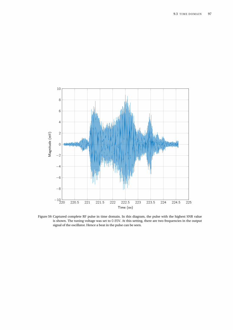
9.3 T I M E D O M A I N 97
220 220.5 221 221.5 222 222.5 223 223.5 224 224.5 225−10
−8
−6
−4
−2
0
2
4
6
8
10
Time (ns)
Mag
nitu
de(m
V)
Figure 59: Captured complete RF pulse in time domain. In this diagram, the pulse with the highest SNR valueis shown. The tuning voltage was set to 0.85V. At this setting, there are two frequencies in the outputsignal of the oscillator. Hence a beat in the pulse can be seen.

98 P U L S E O S C I L L AT O R
60 62 64 66 68 70 72 74 76 78 80 82 84 86 88 90−80
−70
−60
−50
−40
−30
−20
Frequency (GHz)
|Y(f)|
Figure 60: Power density spectrum of the captured pulse, computed with the scope’s built-in FFT algorithm. It canbe seen that there are two peaks instead of one.

10M I X E R
In this chapter the last remaining block, the mixer, is characterized. Like all the other measurements,
the mixer has been characterized on wafer, where the test chip LA246304 was used. In order to provide
the required RF signals, the VNA and two frequency converters were used. Because of a software prob-
lem in the VNA, there was a difference between the configured output power at the VNA and the real
output power of the converters. So the first step in this measurement was to measure the calibration
curve of the converters. Therefore the output of each converter was connected to the E4416A power
meter and the output power was measured for different frequency and VNA power settings. Of course,
the power meter was calibrated before this measurement. Figure 61 shows the measures calibration
data for the converter which will be used to provide the LO signal, Figure 62 shows the calibration data
for the converter used to create the RF signal.
Now the mixer was connected to the converters using Infinity probes and Gore cables with 1-mm con-
nectors, the VBias input was left open and the mixer was supplied with 3.3V. Because of the high output
impedance of the mixer, it could not directly drive the spectrum analyzers input and so an IF-amplifier
provided by Matthias Porranzl was connected in between. Then the IF-output power was measured for
different settings for the LO power, the RF power and the IF frequency. The voltage conversion gain of
the mixer was computed from the output power, where the loss of the arrangement and the gain of
the IF-amplifier was taken into account. Figure 63 shows the voltage conversion gain of the mixer over
the LO power for different RF power settings, Figure 64 shows the voltage conversion gain of the mixer
over the RF power for different LO power settings and Figure 65 shows the voltage conversion gain of
the mixer over frequency.
The measurement results show that the mixer is not working as intended. The cause of the problem
was sought both in the measurement arrangement and in the design of the mixer, where in the latter
it was ultimately found. The mistake in the mixer design was, that the inductance of the connection
between the diodes and the capacitor was not taken into account. Hence, there was no path to ground
for the RF signal at the diodes and the voltage conversion gain has decreased dramatically. A new simu-
lation was made including these inductances, modelled as lumped element inductors. This simulation
has delivered results that correspond to the measurement data. Section 12.1 describes, how this mis-
take can be corrected.
Despite the broken mixer, the complete radar system was measured. Therefore the LA246301 chip was
used. The transmit output and receive input were connected together. The loss of this connection was
about 10dB. However, no meaningful result could be derived due to the large mixer loss.
99

100 M I X E R
−20 −18 −16 −14 −12 −10 −8 −6 −4 −2 0 2 4 6 8 10−25
−20
−15
−10
−5
0
5
10
NWA power setting (dBm)
Conv
erte
rout
putp
ower
(dB
m)
fLO=70GHzfLO=71GHzfLO=72GHzfLO=73GHzfLO=74GHzfLO=75GHzfLO=76GHzfLO=77GHzfLO=78GHzfLO=79GHzfLO=80GHz
Figure 61: Calibration curve for the converter used as LO signal source. It can be seen that the measured outputpower differes from the VNA setting. On the right hand side, the output power of the converter saturates.

M I X E R 101
−25 −20 −15 −10 −5 0 5 10−30
−25
−20
−15
−10
−5
0
5
10
NWA power setting (dBm)
Conv
erte
rout
putp
ower
(dB
m)
fRF=70GHzfRF=71GHzfRF=72GHzfRF=73GHzfRF=74GHzfRF=75GHzfRF=76GHzfRF=77GHzfRF=78GHzfRF=79GHzfRF=80GHz
Figure 62: Calibration curve for the converter used as RF signal source.

102 M I X E R
−9 −8 −7 −6 −5 −4 −3 −2 −1 0−19
−18
−17
−16
−15
−14
−13
LO power (dBm)
Conv
ersio
nga
in(d
B)
PRF=−28.85dBmPRF=−24.07dBmPRF=−8.17dBmPRF=0.42dBm
Figure 63: Measured voltage conversion gain of the mixer vs. LO power for different RF power settings. It can beseen that the measured voltage conversion gain is much lower than the simulated one. With increasingLO power, the voltage conversion gain increases.

M I X E R 103
−30 −25 −20 −15 −10 −5 0 5−19
−18
−17
−16
−15
−14
−13
RF power (dBm)
Conv
ersio
nga
in(d
B)
PLO=−8.54dBmPLO=−6.00dBmPLO=−2.22dBmPLO=−0.63dBm
Figure 64: Measured voltage conversion gain of the mixer vs. RF power for different LO power settings. It can beseen that the voltage conversion gain is almost independent from the RF power.

104 M I X E R
70 71 72 73 74 75 76 77 78 79 80−18
−17
−16
−15
−14
−13
−12
−11
Frequency (GHz)
Conv
ersio
nga
in(d
B)
PRF=−28.85dBmPRF=−24.07dBmPRF=−8.17dBmPRF=0.42dBm
Figure 65: Measured voltage conversion gain of the mixer vs. frequency. It can be seen that the voltage conver-sion gain increases with increasing frequency, but the simulated voltage conversion gain could not bereached.

Part V
S U M M A RY
In the subsequent final part the results are summarized and an outlook into the future,
including an overview of the latest updates, is given.


11C O N C L U S I O N
In this work, the function of 77GHz pulse oscillators could be proven by time domain measurements
to the author’ s knowledge for the first time. It could also be shown, that an appropriate receive path
for a sequential sampling pulse radar can be implement. Hence, with the sequential sampling pulse
radar concept, a power efficient alternative for the FMCW radar is available for the W-Band.
107


12N E X T TA P E O U T
This chapter addresses the changes in the design, which have been made in order to fix the issues
which have been found during the measurements.
12.1 M I X E R
During the measurements presentation in chapter 10 it was encountered, that there has happened a
mistake in the simulation of the mixer. As already explained, the inductance of the wire which con-
nects the diodes to the load capacitor has not been taken into account. Because of the relatively long
wires, this inductance is so high that the capacitor cannot provide an RF ground to the diodes. Hence
the voltage conversion gain of the mixer is too low. The first step to fix this issue has already happened
in between the measurements, where the inductance of the wire was approximated and included into
the simulation. The next step was to include a small load capacitor, which is located very close to the
diode connected transistors. In Figure 66 the layout of the new mixer is shown, where the additional
capacitors are marked with white boxes. Each of the capacitors has a capacitance of 0.6pF. This ca-
pacitor provides a sufficient path to ground for the RF signal, but was selected to be so small that the
influence on the total load capacitance remains small. In the new simulation, a voltage conversion
gain very close to the original simulation results was computed. In order to provide a mechanism to
correct the offset, the bias circuit for the two diode branches was split up. Now the operating point,
including the DC output voltage of each diode branch can be adjusted independently from the other.
Also, the voltage conversion gain of each branch can be adjusted separately, which helps minimizing
the LO rectification offset.
12.2 P O W E R A M P L I F I E R
The power amplifier addresses the issue of the impact of external high quality resonators on the pulse
oscillators tuning behavior as it was shown in Section 9.2. After the function of the pulse oscillator,
especially the coherency of the generated pulses, was proven by measurements, the transmit path can
be extended with a buffer to decouple the oscillator from external resonators. The buffer does not need
to provide a high power gain, but it must be switchable to conform with the idea of power saving. A
single ended power amplifier, which was initially designed by Matthias Porranzl, was re-implemented
and extended with a switch. In Figure 67, the circuit diagram of the designed power amplifier is shown.
The amplifier core is transistor T1, which is connected in common emitter configuration. R7 is used
for emitter degeneration and C3 acts as a bypass for the RF signal. R3, R4, R5 and R6 form the bias
network. T L1 and C1 are the input matching network, T L2 and C2 are the output matching network
with included coupling capacitors.
In order to implement the switching capability, transistor T2 was added. When T2 is on, it shortens the
bias voltage to ground and hence the amplifier is off. R1 provides a high impedance path to ground to
secure that the amplifier is on if the EN input is not connected. Because of the mistake made in the
109

110 N E X T TA P E O U T
Figure 66: Layout of the new mixer. The additional capacitors are marked with the white boxes. They are locatedas close as possible to the diodes and have a capacity of 0.6pF each.
mixer design, the inductance of all connections, especially around T1, have been carefully estimated
and included in the circuit diagram. During simulations it could be seen that L2 has a great impact on
the gain of the amplifier.
The power amplifiers function was verified by simulation. First, the port matching was simulated, the
results show a matching of −10dB or better in a bandwidth of 10GHz around the designed center fre-
quency for both, input and output. The power gain of the amplifier is greater than 3dB in this frequency
range, where a peak gain of 4.18dB was observed. Also, the stability factor of the power amplifier was
checked to avoid that the amplifier oscillates. In an additional simulation, the switching behavior was
checked to secure that the power amplifier won’t start oscillating when it is switched on.

12.2 P O W E R A M P L I F I E R 111
T1
T2
R1
R2
R3
R4
R5
R6
R7
C1
C2
C3
L1
L2L3
L4
T L1
T L2
Input
Bias
Q
EN
Figure 67: Circuit diagram of the designed power amplifier. T1 is the amplifier in common emitter configuration.T2 is used to switch the PA off. L1 and L2 are used to simulate the inductance of the connection to thetransistor.


13F U T U R E W O R K
This chapter concerns the future plans for the sequential sampling pulse radar. The first steps for the
near future have already been made with the updates described in chapter 12, but measurement re-
sults are not available at the time of writing. Also the design of a demonstrator board for the pulse
radar system is pending.
The next big step on the way to a complete single chip radar is the technology shift from the B7 tech-
nology to the B11 technology. In order to improve the pulse radar’s range, an LNA could be included
in the receive path and besides that, the control unit requires an update to provide the enable signals
for the mixer and the new power amplifier. Another big step towards a single chip radar would be to
include the antennas into the package. For 77GHz, antennas-in-package have already been published.
The results from this work also suggest, that it is possible to increase the operating frequency of the
pulse radar to 120GHz. This would enable the antennas to be implemented directly on chip.
113


Part VI
A P P E N D I X


AC H I P L AY O U T S
117

118 C H I P L AY O U T S
Figure 68: Layout of the designed complete pulse radar chip. The orange box marks the mixer, where the trans-mission line of the rat race coupler can be clearly seen. The green boxes show the control units and theyellow boxes show the pulse oscillators. In the upper pink box there is the receive port, the transmit portis in the lower pink box.

C H I P L AY O U T S 119
Figure 69: Layout of the test chip which was designed to measure the pulse oscillators. The green boxes show thecontrol units, the yellow boxes show the pulse oscillators. The pink boxes mark the RF ports.

120 C H I P L AY O U T S
Figure 70: Layout of the test chip for the control unit and for the mixer. The white box shows the comparator, theyellow box shows the monoflop and the green box shows the complete control unit. The mixer is shownin the orange box, its RF port is marked with the upper pink box, the LO port is marked with the lowerpink box.

L I S T O F F I G U R E S
Figure 1 Simplified block diagram of the proposed pulse radar. The pulse generators on
the left hand side generate the transmit signal and the LO signal. The transmit-
ted signal is reflekted from a target on the right hand side. The mixer multiplies
the received signal with the LO signal and the resulting signal is then integrated
over time. . . . . . . . . . . . . . . . . . . . . . . . . . . . . . . . . . . . . . . . . . . 16
Figure 2 Sketch of the signals in time domain. The LO pulse train is shown in the top
most diagram, the received pulse train is shown in the second diagram. All
pulses have the same envelope, but the pulse repetition times are different for
the LO and for the RX pulse train. The phase difference between the LO and
RX pulses increases from one pulse to the next pulse with a constant step. The
third diagram shows the DC-component at the mixer’s output. It was assumed
that the higher frequency mixer products are such small that they can be ne-
glected. Because of the linear increasing phase difference between the LO and
RX pulses, the magnitude of the DC-component at the mixer’s output shows
a sinusoidal behavior. The last diagram shows the output signal of the pulse
radar after the integrator stage. The level of the output signal is constant be-
tween the pulses. . . . . . . . . . . . . . . . . . . . . . . . . . . . . . . . . . . . . . 22
Figure 3 Illustration of radar scenario. On the left hand side, the transmit/receive an-
tenna is shown. At a distance r, the reflecting target (here a corner reflector) is
shown. . . . . . . . . . . . . . . . . . . . . . . . . . . . . . . . . . . . . . . . . . . . 22
Figure 4 Block diagram of the already existing system designed by Martin Jahn. The sys-
tem consists of two monoflop circuits followed by two comparators which con-
trol the two pulse oscillators. The receive section has an LNA, as well as a balun
and a buffer. In the IF-section, there is an active integrator. . . . . . . . . . . . . 31
Figure 5 Block diagram of the updated pulse radar chip LA246301. it can be seen that
the pulse generation part was reused unchanged. The previous IF-stage was re-
placed by the new mixer, where the LO-branch was adopted to meet the mixers
requirements. The LNA in the receive branch was removed. . . . . . . . . . . . 36
Figure 6 Block diagram of the LA246302 test chip which was designed to characterize
the pulse oscillator. Compared to Figure 5 only the mixer was removed and the
LO-signal was connected to an RF-pad. . . . . . . . . . . . . . . . . . . . . . . . . 36
Figure 7 Block diagram of the LA246304 test chip which was designed to characterize
the digital components and the mixer. It can be seen, that each part of the con-
trol unit, as well as the complete control unit, are fully accessible. Also the new
mixer is contained in the chip. . . . . . . . . . . . . . . . . . . . . . . . . . . . . . 37
Figure 8 Circuit diagram of the monoflop. The minimum pulse width is defined by the
capacitor C1. C1 is realized as 4 capacitors which are connected in parallel us-
ing laser fuses. Thus the minimum pulse width can be changed with the fuses.
The pulse width can be extended with the voltage level at the VEN input. . . . . 38
121

122 List of Figures
Figure 9 Simulated pulse width vs. VEN for all meaningful fuse configurations. It can be
seen that a pulse width from 1.5ns up to infinity can be achieved. The mini-
mum pulse width depends on the fuse setting. . . . . . . . . . . . . . . . . . . . . 39
Figure 10 Circuit diagram of the comparator. The comparator is realized as a free running
differential amplifier, which consists of the transistors T1 and T2. At the base of
T2, a reference voltage is applied. When the input voltage is higher than the
reference voltage, the output switches to a high voltage level. . . . . . . . . . . . 39
Figure 11 Simulated characteristic curve of the comparator for different VBias. It can be
seen that the switching threshold voltage increases with increasing bias voltage. 40
Figure 12 Simulated pulse width after the comparator vs. VEN for different VBias. It can
be seen that the minimum pulse width is higher than that one of the single
monoflop (see Figure 10). . . . . . . . . . . . . . . . . . . . . . . . . . . . . . . . . 41
Figure 13 Circuit diagram of the pulse oscillator. The pulse oscillator consists out of a
singled ended Colpitts oscillator and a driver stage. . . . . . . . . . . . . . . . . . 43
Figure 14 Simulated output power vs. VOsc. At the nominal supply voltage of 1.8V, the
oscillator shows an output power of approximately 2dBm. . . . . . . . . . . . . 44
Figure 15 Simulated conversion gain of the oscillator vs. VOsc. The conversion gain is the
quotient of RF output power and the DC input power. It can be seen that the
conversion gain is between −10dB and −12V. . . . . . . . . . . . . . . . . . . . . 45
Figure 16 Simulated output frequency vs. VTune for different settings of VOsc. It can be
seen, that width increasing tuning voltage, the frequency decreases. It can also
be seen, that the oscillation frequency is more sensitive to the supply voltage
than to the tuning voltage. . . . . . . . . . . . . . . . . . . . . . . . . . . . . . . . . 46
Figure 17 Simulated tuning range vs. VOsc. It can be seen that the tuning range is close to
900MHz for the desired operating conditions. . . . . . . . . . . . . . . . . . . . . 47
Figure 18 Simulated transient pulse. The shape of the envelope is almost rectangular
with a small overshooting in the beginning and at the end of the pulse. . . . . . 48
Figure 19 Schematic diagram of a single balanced diode mixer. A rat-race coupler is used
to generate the sum Σ and the difference ∆ signal. The non-linearity of the
diodes is the used to perform the multiplication. The required RF ground is
provided with the capacitor C1. . . . . . . . . . . . . . . . . . . . . . . . . . . . . . 49
Figure 20 Schematic diagram of the designed mixer. Compared to Figure 19, a second
diode branch was added to compensate the DC-offset voltage. . . . . . . . . . . 50
Figure 21 Circuit diagram of the designed mixer. It consists of the rat race coupler shown
on the left, the two diode branches in the middle and the bias current mirror
on the top right side of the diagram. . . . . . . . . . . . . . . . . . . . . . . . . . . 51
Figure 22 Simulated matching of the rat race coupler. It can be seen that a matching of
−20dB or better is achieved in a bandwidth of 20GHz around the design fre-
quency. . . . . . . . . . . . . . . . . . . . . . . . . . . . . . . . . . . . . . . . . . . . 52
Figure 23 Simulated LO-RF isolation of the rat race coupler. It can be seen that an isola-
tion closes to 35dB is achieved at the design frequency. . . . . . . . . . . . . . . 53
Figure 24 Simulated matching of the rectifier. it can be seen, that the matching is better
than 15dB in a bandwidth of 5GHz. Because of the non-linearity of the diodes,
the input impedance depends on the used power. . . . . . . . . . . . . . . . . . . 54

List of Figures 123
Figure 25 Simulated matching of the whole mixer. At the design frequency, a matching
between −30dB and −40dB is achieved. . . . . . . . . . . . . . . . . . . . . . . . 55
Figure 26 Simulated LO-RF isolation of the whole mixer. It can be seen that the isolation
at the design frequency is close to 40dB . . . . . . . . . . . . . . . . . . . . . . . . 56
Figure 27 Simulated voltage conversion gain vs. LO power. When the RF power is small,
the mixer shows a conversion gain close to 0dB. When the RF power is too high,
the mixers saturates and the conversion decreases. . . . . . . . . . . . . . . . . . 57
Figure 28 Simulated voltage conversion gain vs. RF power. It can be seen that the mixer
reaches it’s 1dB-compression point when the RF power is approximatly −7dB.
With increasing LO power, the compression point moves to the right. . . . . . . 58
Figure 29 Simulated voltage conversion gain vs. VEN. It can be seen that the voltage con-
version gain decreases when the mixer is turned off. . . . . . . . . . . . . . . . . 59
Figure 30 Simulated noise figure. It can be seen that the noise figure is between 12dB and
13dB. . . . . . . . . . . . . . . . . . . . . . . . . . . . . . . . . . . . . . . . . . . . . 60
Figure 31 Simulated output noise. The output noise of the mixer is used later to estimate
the SNR of the pulse radar. . . . . . . . . . . . . . . . . . . . . . . . . . . . . . . . 61
Figure 32 Modell of the mixer. Each diode branch is modelled with a current source for
the conversion gain and an additional current source to take the DC-offset into
account. The dependence of the mixers output impedance on the VEN voltage
is taken into account with the switches. . . . . . . . . . . . . . . . . . . . . . . . . 61
Figure 33 Transformed model of the mixer. The two branches from Figure 32 are com-
bined, but the output voltage is still differential. This model is used to calculate
the output signal of the designed pulse radar. . . . . . . . . . . . . . . . . . . . . 62
Figure 34 Simulated LO transconductance of the mixer. The LO transconductance relates
the mixers IF output current to the applied LO magnitude. It can be used to
approximate the DC-offset voltage at the output of the pulse radar. . . . . . . . 62
Figure 35 Simulated LO transconductance of the mixer vs. VEN. It can be seen that the LO
transconductance goes to zero when the mixer is turned off. . . . . . . . . . . . 63
Figure 36 Simulated RF transconductance of the mixer. The RF transconductances re-
lates the mixers IF output current to the magnitude of the RF input voltage. . . 64
Figure 37 Simulated RF transconductance of the mixer vs. VEN. It can be seen that the RF
transconductance is much higher than the LO transconductance. . . . . . . . . 65
Figure 38 Simulated output impedance of the mixer when it is enabled. With increasing
bias voltage, the output impedance decreases because the operating point of
the mixer diodes is shifted towards the conducting region. . . . . . . . . . . . . 66
Figure 39 Simulated output impedance of the mixer vs. VEN. It can be seen that the out-
put impedance increases dramatically when the mixer is turned off. Thus the
integrating capacitor is prevented from discharging which increases the mag-
nitude of the pulse radar’s output signal. . . . . . . . . . . . . . . . . . . . . . . . 67
Figure 40 RC-network used to model the behavior of the mixers output impedance in
combination with the external load capacitor. . . . . . . . . . . . . . . . . . . . . 68
Figure 41 Peak magnitude vs. frequency difference for different fLO with a load capaci-
tor of two times 10pF. It can be seen that the magnitude of the output signal
increases with increasing pulse rate, but when the pulse rate is increased, also
the duration of the radar measurement is increased. . . . . . . . . . . . . . . . . 71

124 List of Figures
Figure 42 Peak magnitude for vs. frequency difference for different load capacitors at
fLO =5MHz. With increasing capacitive load, the magnitude of the output sig-
nal decreases. . . . . . . . . . . . . . . . . . . . . . . . . . . . . . . . . . . . . . . . 72
Figure 43 SNR vs. frequency difference for different fLO with a load capacitor of two times
10pF. For the calculation of the SNR, the output noise of the mixer was used. . 73
Figure 44 SNR vs. frequency difference for different load capacitors at fLO =5MHz. It can
be seen that the SNR behaves like the magnitude of the output voltage shown
in Figure 42. The SNR decreases when the load capacitance is increased. . . . . 74
Figure 45 Sample pulse to illustrate the charging effect which is introduced with the SMA
cable. The red curve indicates the ideal driver output voltage, where the blue
curve shows the voltage measured at the oscilloscope. When the driver output
voltage switches to the high level, the capacitance of the cable is charged and
the voltage at to oscilloscope increases according to the charging curve of a
capacitor. When the driver goes off, the capacitance of the cable is discharged.
The pulse width is measured as the time difference between the green markers. 78
Figure 46 Measured pulse width vs. the voltage level at the EN input. The similarity with
the simulations results (see Figure 9) can be seen. Because of the high cable
capacitance, the measured signal was very low. Hence the results are not very
accurate. . . . . . . . . . . . . . . . . . . . . . . . . . . . . . . . . . . . . . . . . . . 79
Figure 47 Measured characteristic curve of the comparator. It can be seen that the mea-
surement fits well to the simulation results (dashed lines). . . . . . . . . . . . . . 82
Figure 48 Pulsewidth measured at the output of the control unit. It can be seen, that the
measured pulse width corresponds to the simulated pulse width shown in Fig-
ure 46. . . . . . . . . . . . . . . . . . . . . . . . . . . . . . . . . . . . . . . . . . . . 84
Figure 49 Measured output power of the oscillator vs. the supply voltage. The red curve
shows the simulated output power. It can be seen, that the measured output
power is approximatly 7dB lower than the simulated one. . . . . . . . . . . . . . 86
Figure 50 Measured oscillation frequency vs. the tuning voltage for different supply volt-
ages. It can be seen that the oscillation frequency start changing when the tun-
ing voltage reaches the typical diode forward voltage. The result corresponds
to the simulation data. . . . . . . . . . . . . . . . . . . . . . . . . . . . . . . . . . . 88
Figure 51 Tuning range of the oscillator over the supply voltage. It can be seen that the
measured tuning range is between 1.4GHz and 400MHz. . . . . . . . . . . . . . 89
Figure 52 Enlarged section of the oscillation frequency over the tuning voltage showing
the discrete frequency steps. The frequency steps are caused by the high qual-
ity of the used wave guide components. Such a behavior can be avioded with
an additional buffer at the output of the oscillator. . . . . . . . . . . . . . . . . . 90
Figure 53 Sample of two oscillations instead of one close to a frequency step at VTune=0.88V.
When the tuning voltage is changed, the peaks don’t move in frequency. In-
stead, one of the peaks becomes larger and the other one becomes smaller. . . 91
Figure 54 Course of the power at the two peak frequencies over the tuning voltage. It
shows that the peaks changes their magnitude instead of moving in frequency. 92
Figure 55 Spectrum of the oscillators output signal. This measurement was done using
the internal mixer to decouple the oscillator from the measurement setup. The
diagram shows that the output signal of the oscillator has a high bandwidth.
This is because the oscillator is not stabilized. . . . . . . . . . . . . . . . . . . . . 93

List of Figures 125
Figure 56 Screenshot of the sampling scope showing the pulses generated from the pulse
oscillator. The following setting was used: VOsc = 2.3V, VLogic=2.6V, VTune = 0.85V. 94
Figure 57 Measured SNR over VOsc and VLogic with VTune=0V. The diagram shows the
range of VOsc and VLogic where the oscillator is coherent. . . . . . . . . . . . . . . 95
Figure 58 Measured SNR over VOsc and VLogic with VTune=0.85V. Compared to Figure 57,
the diagram shows a larger coherence region and a higher SNR was measured.
A drawback is that at this level of the tuning voltage, the oscillator generates
two frequencies instead of a single one. . . . . . . . . . . . . . . . . . . . . . . . 96
Figure 59 Captured complete RF pulse in time domain. In this diagram, the pulse with
the highest SNR value is shown. The tuning voltage was set to 0.85V. At this
setting, there are two frequencies in the output signal of the oscillator. Hence a
beat in the pulse can be seen. . . . . . . . . . . . . . . . . . . . . . . . . . . . . . . 97
Figure 60 Power density spectrum of the captured pulse, computed with the scope’s built-
in FFT algorithm. It can be seen that there are two peaks instead of one. . . . . 98
Figure 61 Calibration curve for the converter used as LO signal source. It can be seen that
the measured output power differes from the VNA setting. On the right hand
side, the output power of the converter saturates. . . . . . . . . . . . . . . . . . . 100
Figure 62 Calibration curve for the converter used as RF signal source. . . . . . . . . . . . 101
Figure 63 Measured voltage conversion gain of the mixer vs. LO power for different RF
power settings. It can be seen that the measured voltage conversion gain is
much lower than the simulated one. With increasing LO power, the voltage
conversion gain increases. . . . . . . . . . . . . . . . . . . . . . . . . . . . . . . . . 102
Figure 64 Measured voltage conversion gain of the mixer vs. RF power for different LO
power settings. It can be seen that the voltage conversion gain is almost inde-
pendent from the RF power. . . . . . . . . . . . . . . . . . . . . . . . . . . . . . . 103
Figure 65 Measured voltage conversion gain of the mixer vs. frequency. It can be seen
that the voltage conversion gain increases with increasing frequency, but the
simulated voltage conversion gain could not be reached. . . . . . . . . . . . . . 104
Figure 66 Layout of the new mixer. The additional capacitors are marked with the white
boxes. They are located as close as possible to the diodes and have a capacity
of 0.6pF each. . . . . . . . . . . . . . . . . . . . . . . . . . . . . . . . . . . . . . . . 110
Figure 67 Circuit diagram of the designed power amplifier. T1 is the amplifier in common
emitter configuration. T2 is used to switch the PA off. L1 and L2 are used to
simulate the inductance of the connection to the transistor. . . . . . . . . . . . . 111
Figure 68 Layout of the designed complete pulse radar chip. The orange box marks the
mixer, where the transmission line of the rat race coupler can be clearly seen.
The green boxes show the control units and the yellow boxes show the pulse
oscillators. In the upper pink box there is the receive port, the transmit port is
in the lower pink box. . . . . . . . . . . . . . . . . . . . . . . . . . . . . . . . . . . 118
Figure 69 Layout of the test chip which was designed to measure the pulse oscillators.
The green boxes show the control units, the yellow boxes show the pulse oscil-
lators. The pink boxes mark the RF ports. . . . . . . . . . . . . . . . . . . . . . . . 119

126 List of Figures
Figure 70 Layout of the test chip for the control unit and for the mixer. The white box
shows the comparator, the yellow box shows the monoflop and the green box
shows the complete control unit. The mixer is shown in the orange box, its RF
port is marked with the upper pink box, the LO port is marked with the lower
pink box. . . . . . . . . . . . . . . . . . . . . . . . . . . . . . . . . . . . . . . . . . . 120

L I S T O F A B B R E V I AT I O N S
33520A Keysight, 80MHz function / arbitrary waveform generator . . . . . . . . . . . . . . . . . . . . . . . 77
33522A Keysight, 30MHz function/arbitrary waveform generator . . . . . . . . . . . . . . . . . . . . . . . . 87
DICE GmbH & Co KG Danube Integrated Circuit Engineering
(majority owned by Infineon Technologies)
Freistädter Straße 400, A-4040 Linz, Austria
. . . . . . . . . . . . . . . . . . . . . . . . . . . . . . . . . . . . . . . . . . . . . . . . . . . . . . . . . . . . . . . . . . . . . . . . . . . . . . . . . . . . . . 5
CW Continous wave . . . . . . . . . . . . . . . . . . . . . . . . . . . . . . . . . . . . . . . . . . . . . . . . . . . . . . . . . . . . . . . . . . . . 42
DC Direct current . . . . . . . . . . . . . . . . . . . . . . . . . . . . . . . . . . . . . . . . . . . . . . . . . . . . . . . . . . . . . . . . . . . . . . 33
DCA X 86100D Keysight, 80GHz Infiniium DCA-X wide-bandwidth oscilloscope . . . . . . . . . . . . . . . . 87
E4416A Keysight, Single channel power meter . . . . . . . . . . . . . . . . . . . . . . . . . . . . . . . . . . . . . . . . . . . . . 85
E5052A Keysight, Signal source analyzer . . . . . . . . . . . . . . . . . . . . . . . . . . . . . . . . . . . . . . . . . . . . . . . . . . . 85
EMI Electromagnetic interference . . . . . . . . . . . . . . . . . . . . . . . . . . . . . . . . . . . . . . . . . . . . . . . . . . . . . . 32
EYE-Pass Cascade Microtech, High performance DC probes . . . . . . . . . . . . . . . . . . . . . . . . . . . . . . . . 77
FFT Fast fourier transformation . . . . . . . . . . . . . . . . . . . . . . . . . . . . . . . . . . . . . . . . . . . . . . . . . . . . . . . . 87
FMCW Frequency modulated continous wave . . . . . . . . . . . . . . . . . . . . . . . . . . . . . . . . . . . . . . . . . . . . 11
gm-C A voltage controlled current source which drives a capacitor . . . . . . . . . . . . . . . . . . . . . 33
HP34401A Keysight, 6.5 digit digital multimeter . . . . . . . . . . . . . . . . . . . . . . . . . . . . . . . . . . . . . . . . . . . . . . 81
IF intermediate frequency . . . . . . . . . . . . . . . . . . . . . . . . . . . . . . . . . . . . . . . . . . . . . . . . . . . . . . . . . . . . 35
Infinity probes Cascade Microtech, 110GHz RF probes . . . . . . . . . . . . . . . . . . . . . . . . . . . . . . . . . . . . . . . . . . . 85
LA246301 Complete pulse radar chip . . . . . . . . . . . . . . . . . . . . . . . . . . . . . . . . . . . . . . . . . . . . . . . . . . . . . . . . 35
LA246302 Testchip for the pulse oscillators . . . . . . . . . . . . . . . . . . . . . . . . . . . . . . . . . . . . . . . . . . . . . . . . . . 36
LA246304 Testchip for the control unit and the mixer . . . . . . . . . . . . . . . . . . . . . . . . . . . . . . . . . . . . . . . . 36
LNA Low noise amplifier . . . . . . . . . . . . . . . . . . . . . . . . . . . . . . . . . . . . . . . . . . . . . . . . . . . . . . . . . . . . . . . . 33
LO Local oscillator . . . . . . . . . . . . . . . . . . . . . . . . . . . . . . . . . . . . . . . . . . . . . . . . . . . . . . . . . . . . . . . . . . . . . 15
M8190A Keysight, 12G Sas arbitrary waveform generator . . . . . . . . . . . . . . . . . . . . . . . . . . . . . . . . . . . 87
NWA vector network analyzer . . . . . . . . . . . . . . . . . . . . . . . . . . . . . . . . . . . . . . . . . . . . . . . . . . . . . . . . . . . 87
pac-simulation periodic ac simulation . . . . . . . . . . . . . . . . . . . . . . . . . . . . . . . . . . . . . . . . . . . . . . . . . . . . . . . . . . . . . 60
PLL Phase locked loop . . . . . . . . . . . . . . . . . . . . . . . . . . . . . . . . . . . . . . . . . . . . . . . . . . . . . . . . . . . . . . . . . . 32
pnoise-simulation periodic noise simulation . . . . . . . . . . . . . . . . . . . . . . . . . . . . . . . . . . . . . . . . . . . . . . . . . . . . . . . . 38
psp-simulation periodic scattering parameter simulation . . . . . . . . . . . . . . . . . . . . . . . . . . . . . . . . . . . . . . . . . 50
pss-simulation periodic steady state simulation . . . . . . . . . . . . . . . . . . . . . . . . . . . . . . . . . . . . . . . . . . . . . . . . . . . 38
RF Radio frequency . . . . . . . . . . . . . . . . . . . . . . . . . . . . . . . . . . . . . . . . . . . . . . . . . . . . . . . . . . . . . . . . . . . . . 5
RTO1024 Rhode&Schwarz, 2GHz digital oscilloscope . . . . . . . . . . . . . . . . . . . . . . . . . . . . . . . . . . . . . . . 77
127

128 L I S T O F A B B R E V I AT I O N S
RX Receive . . . . . . . . . . . . . . . . . . . . . . . . . . . . . . . . . . . . . . . . . . . . . . . . . . . . . . . . . . . . . . . . . . . . . . . . . . . . . 17
SNR Signal to noise ratio . . . . . . . . . . . . . . . . . . . . . . . . . . . . . . . . . . . . . . . . . . . . . . . . . . . . . . . . . . . . . . . . 35
sp-simulation scattering parameter simulation . . . . . . . . . . . . . . . . . . . . . . . . . . . . . . . . . . . . . . . . . . . . . . . . . . 60
TOE8842-24 Toellner, 2 channel programmable power supply . . . . . . . . . . . . . . . . . . . . . . . . . . . . . . . . . 77

L I S T O F M AT H E M AT I C A L S Y M B O L S
TLO Pulse repetition time of the LO signal . . . . . . . . . . . . . . . . . . . . . . . . . . . . . . . . . . . . . . . . . . . . . . . . . . . 15
TRX Pulse repetition time of the RX signal . . . . . . . . . . . . . . . . . . . . . . . . . . . . . . . . . . . . . . . . . . . . . . . . . . . 15
Tp Pulse width . . . . . . . . . . . . . . . . . . . . . . . . . . . . . . . . . . . . . . . . . . . . . . . . . . . . . . . . . . . . . . . . . . . . . . . . . . . . . . 15
ω0 Angular oscillaton frequency of the pulse oscillators . . . . . . . . . . . . . . . . . . . . . . . . . . . . . . . . . . . 16
sTX (t ) Transmit signal . . . . . . . . . . . . . . . . . . . . . . . . . . . . . . . . . . . . . . . . . . . . . . . . . . . . . . . . . . . . . . . . . . . . . . . . . . 16
r Distance to the radar target . . . . . . . . . . . . . . . . . . . . . . . . . . . . . . . . . . . . . . . . . . . . . . . . . . . . . . . . . . . . . 16
sRX (t ) Received signal . . . . . . . . . . . . . . . . . . . . . . . . . . . . . . . . . . . . . . . . . . . . . . . . . . . . . . . . . . . . . . . . . . . . . . . . . . 16
sLO (t ) LO signal . . . . . . . . . . . . . . . . . . . . . . . . . . . . . . . . . . . . . . . . . . . . . . . . . . . . . . . . . . . . . . . . . . . . . . . . . . . . . . . . . 16
sIF (t ) Mixer output signal . . . . . . . . . . . . . . . . . . . . . . . . . . . . . . . . . . . . . . . . . . . . . . . . . . . . . . . . . . . . . . . . . . . . . . 16
y (t ) Output signal of the pulse radar . . . . . . . . . . . . . . . . . . . . . . . . . . . . . . . . . . . . . . . . . . . . . . . . . . . . . . . . . 16
∆T Difference between the pulse repetition times . . . . . . . . . . . . . . . . . . . . . . . . . . . . . . . . . . . . . . . . . . 17
τRT Round trip delay time . . . . . . . . . . . . . . . . . . . . . . . . . . . . . . . . . . . . . . . . . . . . . . . . . . . . . . . . . . . . . . . . . . . 17
p (t ) One pulse . . . . . . . . . . . . . . . . . . . . . . . . . . . . . . . . . . . . . . . . . . . . . . . . . . . . . . . . . . . . . . . . . . . . . . . . . . . . . . . . 17
e (t ) Normalized and time limited envelope of the pulse . . . . . . . . . . . . . . . . . . . . . . . . . . . . . . . . . . . . 17
rect(t ) Rectangular shaped function . . . . . . . . . . . . . . . . . . . . . . . . . . . . . . . . . . . . . . . . . . . . . . . . . . . . . . . . . . . . 17
h (t ) Normalized envelope of the pulse . . . . . . . . . . . . . . . . . . . . . . . . . . . . . . . . . . . . . . . . . . . . . . . . . . . . . . . 17
A0 Magnitude of a transmit pulse . . . . . . . . . . . . . . . . . . . . . . . . . . . . . . . . . . . . . . . . . . . . . . . . . . . . . . . . . . 18
αRT Round trip gain factor . . . . . . . . . . . . . . . . . . . . . . . . . . . . . . . . . . . . . . . . . . . . . . . . . . . . . . . . . . . . . . . . . . . 18
αM Mixer voltage gain . . . . . . . . . . . . . . . . . . . . . . . . . . . . . . . . . . . . . . . . . . . . . . . . . . . . . . . . . . . . . . . . . . . . . . . 18
φxx (τ) Autocorrelation function . . . . . . . . . . . . . . . . . . . . . . . . . . . . . . . . . . . . . . . . . . . . . . . . . . . . . . . . . . . . . . . . 20
rxx (τ) Normalized autocorrelation function . . . . . . . . . . . . . . . . . . . . . . . . . . . . . . . . . . . . . . . . . . . . . . . . . . . 20
PTX Transmitted power . . . . . . . . . . . . . . . . . . . . . . . . . . . . . . . . . . . . . . . . . . . . . . . . . . . . . . . . . . . . . . . . . . . . . . 23
A Spherical surface . . . . . . . . . . . . . . . . . . . . . . . . . . . . . . . . . . . . . . . . . . . . . . . . . . . . . . . . . . . . . . . . . . . . . . . . 23
SU Power density of an undirected radiator . . . . . . . . . . . . . . . . . . . . . . . . . . . . . . . . . . . . . . . . . . . . . . . . 23
G Antenna gain . . . . . . . . . . . . . . . . . . . . . . . . . . . . . . . . . . . . . . . . . . . . . . . . . . . . . . . . . . . . . . . . . . . . . . . . . . . . 23
129

130 L I S T O F M AT H E M AT I C A L S Y M B O L S
SD Power density of a directed radiator . . . . . . . . . . . . . . . . . . . . . . . . . . . . . . . . . . . . . . . . . . . . . . . . . . . . . 23
PR Reflected Power . . . . . . . . . . . . . . . . . . . . . . . . . . . . . . . . . . . . . . . . . . . . . . . . . . . . . . . . . . . . . . . . . . . . . . . . . 23
σ Radar target cross section . . . . . . . . . . . . . . . . . . . . . . . . . . . . . . . . . . . . . . . . . . . . . . . . . . . . . . . . . . . . . . . 23
SRX Received power density . . . . . . . . . . . . . . . . . . . . . . . . . . . . . . . . . . . . . . . . . . . . . . . . . . . . . . . . . . . . . . . . . 23
PRX Received power . . . . . . . . . . . . . . . . . . . . . . . . . . . . . . . . . . . . . . . . . . . . . . . . . . . . . . . . . . . . . . . . . . . . . . . . . . 23
Aeff Effective antenna area . . . . . . . . . . . . . . . . . . . . . . . . . . . . . . . . . . . . . . . . . . . . . . . . . . . . . . . . . . . . . . . . . . . 23
Ageo Geometric antenna area . . . . . . . . . . . . . . . . . . . . . . . . . . . . . . . . . . . . . . . . . . . . . . . . . . . . . . . . . . . . . . . . . 23
Ka Antenna efficiency. . . . . . . . . . . . . . . . . . . . . . . . . . . . . . . . . . . . . . . . . . . . . . . . . . . . . . . . . . . . . . . . . . . . . . . 23
λ Wavelength . . . . . . . . . . . . . . . . . . . . . . . . . . . . . . . . . . . . . . . . . . . . . . . . . . . . . . . . . . . . . . . . . . . . . . . . . . . . . . 23
c Propagation speed of light. . . . . . . . . . . . . . . . . . . . . . . . . . . . . . . . . . . . . . . . . . . . . . . . . . . . . . . . . . . . . . . 23
f Frequency of the wave . . . . . . . . . . . . . . . . . . . . . . . . . . . . . . . . . . . . . . . . . . . . . . . . . . . . . . . . . . . . . . . . . . . 23
a Edge length of a corner cube . . . . . . . . . . . . . . . . . . . . . . . . . . . . . . . . . . . . . . . . . . . . . . . . . . . . . . . . . . . . 24
g (t ) Impulse response . . . . . . . . . . . . . . . . . . . . . . . . . . . . . . . . . . . . . . . . . . . . . . . . . . . . . . . . . . . . . . . . . . . . . . . . 25
G (s) Transfer function . . . . . . . . . . . . . . . . . . . . . . . . . . . . . . . . . . . . . . . . . . . . . . . . . . . . . . . . . . . . . . . . . . . . . . . . 25
x? Maximum magnitude of the integrator input signal . . . . . . . . . . . . . . . . . . . . . . . . . . . . . . . . . . . . 25
y? Maximum magnitude of the output signal . . . . . . . . . . . . . . . . . . . . . . . . . . . . . . . . . . . . . . . . . . . . . . 25
n? Shift of the maximum of the output signal . . . . . . . . . . . . . . . . . . . . . . . . . . . . . . . . . . . . . . . . . . . . . . 25
nmax Index of the maximum of the output signal . . . . . . . . . . . . . . . . . . . . . . . . . . . . . . . . . . . . . . . . . . . . . 25
JCC Cycle-to-cycle-jitter . . . . . . . . . . . . . . . . . . . . . . . . . . . . . . . . . . . . . . . . . . . . . . . . . . . . . . . . . . . . . . . . . . . . . 38
g mRF,j singled ended RF transconductance . . . . . . . . . . . . . . . . . . . . . . . . . . . . . . . . . . . . . . . . . . . . . . . . . . . . 60
g mLO,j singled ended LO transconductance . . . . . . . . . . . . . . . . . . . . . . . . . . . . . . . . . . . . . . . . . . . . . . . . . . . . 60
g mLO LO transconductance. . . . . . . . . . . . . . . . . . . . . . . . . . . . . . . . . . . . . . . . . . . . . . . . . . . . . . . . . . . . . . . . . . . . 60
g mRF RF transconductance . . . . . . . . . . . . . . . . . . . . . . . . . . . . . . . . . . . . . . . . . . . . . . . . . . . . . . . . . . . . . . . . . . . . 60
ALO Magnitude of the LO signal . . . . . . . . . . . . . . . . . . . . . . . . . . . . . . . . . . . . . . . . . . . . . . . . . . . . . . . . . . . . . . 68
∆x[n] Difference between two consecutive steps . . . . . . . . . . . . . . . . . . . . . . . . . . . . . . . . . . . . . . . . . . . . . . 69
τRC Lossy integrator time constant . . . . . . . . . . . . . . . . . . . . . . . . . . . . . . . . . . . . . . . . . . . . . . . . . . . . . . . . . . 69
∆ f Difference between LO and RX pulse rate . . . . . . . . . . . . . . . . . . . . . . . . . . . . . . . . . . . . . . . . . . . . . . . 70
fLO LO Pulse rate . . . . . . . . . . . . . . . . . . . . . . . . . . . . . . . . . . . . . . . . . . . . . . . . . . . . . . . . . . . . . . . . . . . . . . . . . . . . 70

B I B L I O G R A P H Y
[1] J. Bock, H. Schafer, H. Knapp, K. Aufinger, M. Wurzer, S. Boguth, T. Bottner, R. Stengl,
W. Perndl, and T. Meister, “3.3 ps SiGe bipolar technology,” in Electron Devices Meeting,
2004. IEDM Technical Digest. IEEE International, 2004, pp. 255–258. [Online]. Available:
http://ieeexplore.ieee.org/stamp/stamp.jsp?arnumber=1419124 (Cited on pages 11 and 29.)
[2] S. Schuster, S. Scheiblhofer, R. Feger, and A. Stelzer, “Signal model and statistical analysis for the
sequential sampling pulse radar technique,” in Radar Conference, 2008. RADAR’08. IEEE. IEEE,
2008, pp. 1–6. (Cited on pages 11 and 15.)
[3] C. G. Diskus, Mikrowellensensorik, 15. Auflage, a. Univ.-prof. Dipl.-Ing. Dr. Christian G. Diskus, Ed.
Johannes Kepler Universität Linz, Institut für Mikroelektronik und Mikrosensorik, 2013. (Cited on
page 15.)
[4] H.-J. Bartsch, Taschenbuch mathematischer Formeln für Ingenieure und Naturwissenschaftler,
M. Sachs, Ed. Hanser Verlag, 2014. (Cited on pages 18, 25, and 69.)
[5] J. Bock, H. Schafer, K. Aufinger, R. Stengl, S. Boguth, R. Schreiter, M. Rest, H. Knapp, M. Wurzer,
W. Perndl, T. Bottner, and T. Meister, “SiGe bipolar technology for automotive radar applications,”
in Bipolar/BiCMOS Circuits and Technology, 2004. Proceedings of the 2004 Meeting, 2004,
pp. 84–87. [Online]. Available: http://ieeexplore.ieee.org/stamp/stamp.jsp?arnumber=1365751
(Cited on page 29.)
[6] W. Scheiblhofer, “Pulsgenerator für 24 GHz Pulsradar,” seminar work, Johannes Kepler Universität
Linz, Institute for Communications Engineering and RF-Systems. (Cited on page 31.)
[7] S. Labs, “Si5341/40 low-jitter, 10-output, any-frequency, any-output clock generator,” Silicon
Labs, Tech. Rep., 2015. (Cited on page 31.)
[8] B. Prammer, “Passive planare Mischer bei 24 GHz und 77 GHz für ein Nahbereichs-Pulsradar,”
Master’s thesis, Johannes Kepler Universität Linz, Institute for Communications Engineering and
RF-Systems, 2011. (Cited on pages 35 and 87.)
[9] H. Ng, M. Jahn, R. Feger, C. Wagner, and A. Stelzer, “An efficient SiGe double-balanced mixer
with a differential rat-race coupler,” in Microwave Integrated Circuits Conference (EuMIC), 2013
European, 2013, pp. 580–583. [Online]. Available: http://ieeexplore.ieee.org/stamp/stamp.jsp?
arnumber=6687915 (Cited on pages 35, 48, 49, and 50.)
[10] C. G. Diskus, Hochfrequenztechnik 2, 6. Auflage, a. Univ.-prof. Dipl.-Ing. Dr. Christian G. Diskus,
Ed. Johannes Kepler Universität Linz, Institut für Mikroelektronik und Mikrosensorik, 2013.
(Cited on page 49.)
[11] W. Perndl, H. Knapp, K. Aufinger, T. Meister, W. Simburger, and A. Scholtz, “Voltage-controlled
oscillators up to 98 GHz in SiGe bipolar technology,” vol. 39, no. 10, pp. 1773–1777, 2004. [Online].
Available: http://ieeexplore.ieee.org/stamp/stamp.jsp?arnumber=1337009 (Cited on page 87.)
131


D E C L A R AT I O N
I declare under penalty of perjury, that I have written this thesis independently and without assistance,
other than those specified sources and aids not being used, or the letter or in spirit taken places have
designated as such. This master thesis is identical to the text document transmitted electronically
E I D E S S TAT T L I C H E E R K L Ä R U N G
Ich erkläre an Eides statt, dass ich die vorliegende Masterarbeit selbstständig und ohne fremde Hilfe
verfasst, andere als die angegebenen Quellen und Hilfsmittel nicht benutzt bzw. die wörtlich oder sin-
ngemäß entnommenen Stellen als solche kenntlich gemacht habe. Die vorliegende Masterarbeit ist
mit dem elektronisch übermittelten Textdokument identisch
Linz, January 2016
Alexander Leibetseder, BSc
133