6.334 power electronics spring 2007 for … chapter 5. introduction to dc/dc converters 3. control...
TRANSCRIPT

MIT OpenCourseWare http://ocw.mit.edu
6.334 Power Electronics Spring 2007
For information about citing these materials or our Terms of Use, visit: http://ocw.mit.edu/terms .

∑
Chapter 5
Introduction to DC/DC
Converters
Analysis techniques: Average KVL, KCL, P.S.S. Conditions.
KCL
I1
i2
in
Figure 5.1: KCL
ij = 0 (5.1)
34

∫
∑
∫
∫
∑
35
Average over time:
1 ∑ ij = 0
T T ∑ 1 ∫
T T ij = 0
∑ < ij > = 0 (5.2)
KCL applies to average current as well as instantaneous currents. (Derives from
conservation of charge).
KVL
V2
Vn
V1
+
−
+
−
+ −
Figure 5.2: KVL
Vk = 0 (5.3)
Average over time:
1 ∑ Vk = 0
T T ∑ 1
Vk = 0 T T
< Vk > = 0 (5.4)
∑
∑
36 CHAPTER 5. INTRODUCTION TO DC/DC CONVERTERS
KVL applies to averaged variables.
P.S.S.
To analyze converters in Periodic Steady State (P.S.S.):
Average KCL < ij > = 0 (5.5)
Average KVL < Vk > = 0 (5.6)
diLfrom < VL > = L < >
dt diL
in P.S.S. < > = 0 dt
Inductor in P.S.S. < VL > = 0 (5.7)
dVLfrom < iC > = C < >
dt dVL
in P.S.S. < > = 0 dt
Capacitor in P.S.S. < iC > = 0 (5.8)
If Circuit is Lossless: Pin = Pout (5.9)
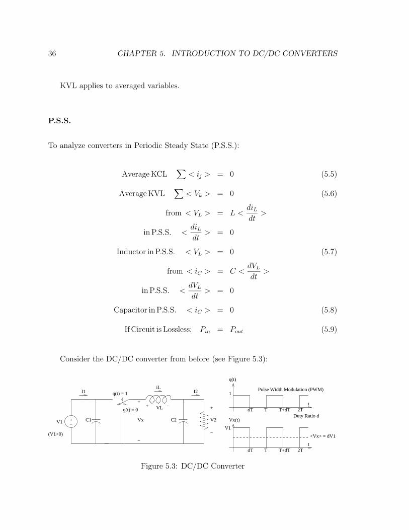
Consider the DC/DC converter from before (see Figure 5.3):
q(t)
iL I2 1
Pulse Width Modulation (PWM)
+−
I1 q(t) = 1
+ t +q(t) = 0
+ VL − dT T T+dT 2T
Duty Ratio dVx C2 V2 Vx(t)V1 C1
V1−(V1>0) <Vx> = dV1
− t
dT T T+dT 2T
Figure 5.3: DC/DC Converter

37
Assume L’s and C’s are very big, therefore:
vC (t) VC (5.10) ≃
iL(t) IL (5.11) ≃
Analyze (using average relations) in P.S.S.:
< VL > = 0
< VL > = dT (V1 − V2) + (1 − d)T (−V2)
dV1T − V2T = 0
V2 = dV1 (5.12)
(Since < VL >= 0, < V2 >=< Vx >= dV1.)
Consider currents:
< iC2 > = 0
I1 = I2 (5.13)
< iC1 > = 0
IC1 = (I1 − I2dT ) + I1(1 − d)T = 0
I1 = dI2 (5.14)
Combining:
I1 = dI2
dV1 = V2
dV1I1 = dI2V2
V1I1 = I2V2 (5.15)

38 CHAPTER 5. INTRODUCTION TO DC/DC CONVERTERS
Therefore, power is (ideally) conserved.
Note: Trick in this type of “average” analysis is to be careful when one can use
an average value and when one must consider instantaneous quantities.
With the following type of external network and V1, V2 > 0, power flows from
1 2. →
Switch implementation: “buck” or “down” converter (see Figure 5.4).
+V1 C2
+
V2C1 −
−
Figure 5.4: Buck (down) Converter
Type of “direct” converter because a DC path exists between input and output
in one switch state.
Suppose we change the location of source and load: Refine switching function so
q(t) = 1 when switch is in down position (see Figure 5.5).
Similar analysis:
< VL > = 0
(V1 − V2)(1 − d)T + V1dT = 0
1 V2 = V1 (5.16)
1 − d
By conservation of power:
I2 = (1 − d)I1 (5.17)

39
q(t)
1
iL t I2I1 q(t) = 0 dT T T+dT 2T
+
-+
Vx(t)- ++ q(t) = 1 VL V2
V2 C1 Vx C2 V1
t - dT T T+dT 2T
-VL
dT T
V1
V1-V2
Figure 5.5: Change the Location of Source and Load
In this case, energy flows from 2 1 and the P.S.S. output voltage (V2) is higher ←
than input voltage (V1).
With the following switch implementation: “boost” or “up” converter. Another
type of “direct” converter (see Figure 5.6).
C2C1V2
+
+ V1
−
−
Figure 5.6: Boost (up) Converter
In general power flows direction depends on:
1. External network
2. Switch implementation

40 CHAPTER 5. INTRODUCTION TO DC/DC CONVERTERS
3. Control
We may need to know all of these to determine behavior.
The boost converter is often drawn with power flowing left to right. However,
there is nothing fundamental about this (see Figure 5.7).
C1C2+V1 V2
+
− −
Figure 5.7: Boost (up) Converter Drawn Left to Right
Boost: Switch turns on and incrementally stores energy from V1 in L. Switch
truns off and this energy and additional energy from input is transferred to output.
Therefore, L used as a temporary storage element.
Either the buck or boost can be seen as the appropriate connection of a canonical
cell (see Figure 5.8).
A
B
C
Figure 5.8: Direct Canonical Cell
The “direct” connection has B as the common node. The rest of operation is
determined by external network, switch implementation and control.
Switch implementation: Different switches can carry current and block voltage
only in certain directions.

41
MOSFET can block positive V and can carry positive or negative i (see Figure 5.9).
D
D
i
+G V
− Body Diode
G
S
S
Figure 5.9: MOSFET
BJT (or darlington) is similar, but negative V blows up device (see Figure 5.10).
i i
+ +Same for V V − IGBT −
Figure 5.10: BJT
Combine elements:
1. Block positive V and carry positive and negative i (see Figure 5.11).
+
V
i
−
Figure 5.11: Combine Elements 1
2. Block positive and negative V and carry positive i (see Figure 5.12).

42 CHAPTER 5. INTRODUCTION TO DC/DC CONVERTERS
i
+
V
−
Figure 5.12: Combine Elements 2
3. Block positive and negative V and carry positive and negative i (see Fig
ure 5.13).
i
+
V
−
Figure 5.13: Combine Elements 3
We can also construct indirect DC/DC converters. Store energy from input, trans
fer energy to output, never a DC path from input to output (see Figure 5.14).
++ BA
V1 V2
−−
C
Figure 5.14: Canonical Cell
Split capacitor (see Figure 5.15):

43
q(t) = 1 q(t) = 0
+ −
q(t) +
V1 V2 1
t− dT T T+dT 2T
q(t) = 0 q(t) = 1
V2
V1
VL
TdT C2
+
V2 −
− C1V1 +
Split Capacitor
Figure 5.15: Indirect DC/DC Converter
< VL > = 0
< VL > = V1dT + (1 − d)TV2
d V2 = V1 (5.18) −
1 − d
V2for 0 < d < 1 → −∞ < < 0 (5.19)
V1
• Store energy in L(dT ) from V1.
• Discharge it (the other way) in V2. (must have voltage inversion).
“Buck/Boost” or “up/down” converter (see Figure 5.16):
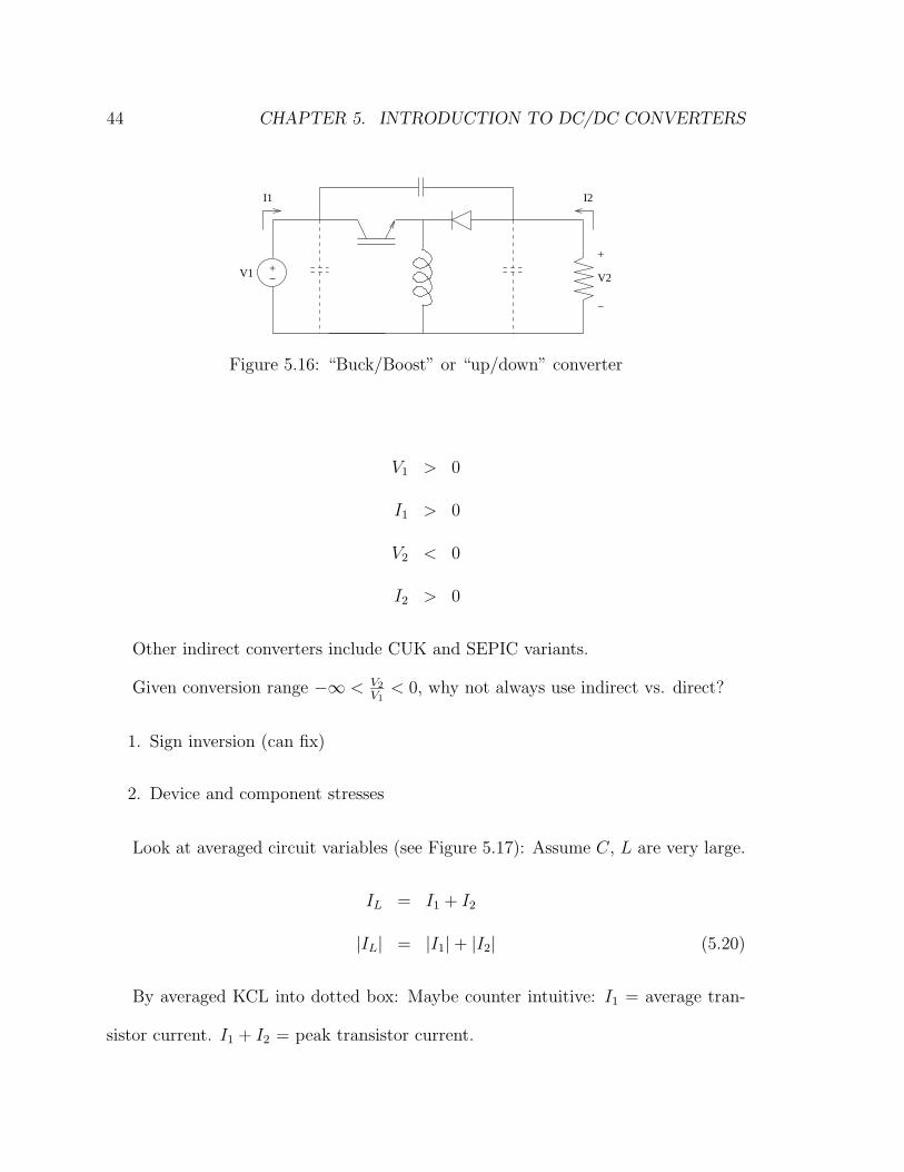
44 CHAPTER 5. INTRODUCTION TO DC/DC CONVERTERS
V1 + +
V2
I2I1
−
−
Figure 5.16: “Buck/Boost” or “up/down” converter
V1 > 0
I1 > 0
V2 < 0
I2 > 0
Other indirect converters include CUK and SEPIC variants.
Given conversion range −∞ < V2 < 0, why not always use indirect vs. direct?V1
1. Sign inversion (can fix)
2. Device and component stresses
Look at averaged circuit variables (see Figure 5.17): Assume C, L are very large.
IL = I1 + I2
|IL| = |I1| + |I2| (5.20)
By averaged KCL into dotted box: Maybe counter intuitive: I1 = average tran
sistor current. I1 + I2 = peak transistor current.

45
V1 + +
V2
I2I1
+
IL iq
VC
−
−
−
iq
I1+I2
I1
dT T
Figure 5.17: Averaged Circuit Variables
By averaged KVL around loop:
VC = V1 − V2
|VC | = |V1| + |V2| (5.21)
Therefore, for big L, C (see Figure 5.18):
V1 + +
V2
I2I1
Q D
V1−V2
I1+I2−
−
−+
Figure 5.18: Big L, C
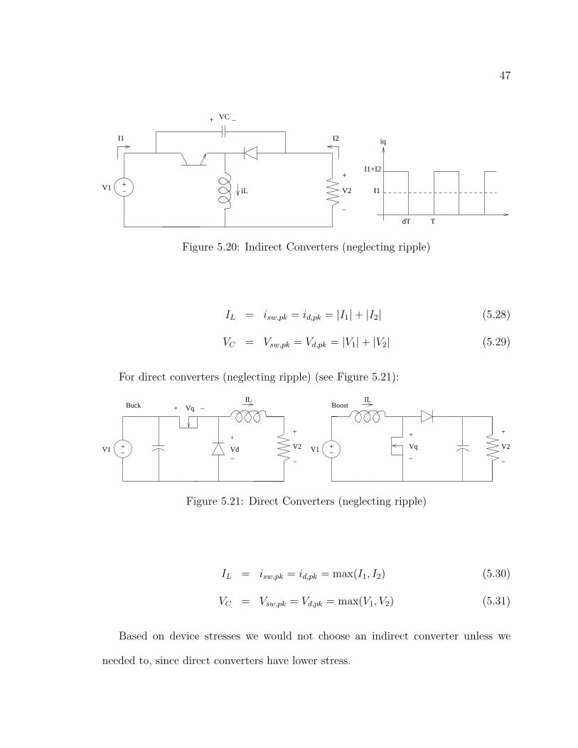
Indirect converter:
So Q, D, L see peak current I = I1 + I2,
Q, D, C block peak voltage V = V1 + V2 .| | | |
Consider direct converters (see Figure 5.19):

46 CHAPTER 5. INTRODUCTION TO DC/DC CONVERTERS
+
I1 Boost D
Q Vq
Buck
+
Vq+ I2
Vd
Q
DC V2
+
V1 +
+
− V1 +
− −−
−
− −
V2C
Figure 5.19: Direct Converters
Buck:
VC = Vq,max = Vd,max = V1 (5.22)
IL = iq,max = id,max = I2 (5.23)
Boost:
VC = Vq,max = Vd,max = V2 (5.24)
IL = iq,max = id,max = I1 (5.25)
Direct converters (either type):
VC = Vq,max = Vd,max = max(V1, V2) (5.26)
IL = iq,max = id,max = max(I1, I2) (5.27)
Device voltage and current stresses are higher for indirect converters than for
direct converters with same power. Inductor current and capacitor voltage are also
higher.
Summary:
For indirect converters (neglecting ripple) (see Figure 5.20):
47
VC+ −
V1 + +
V2
I2I1
iL−
−
iq
I1+I2
I1
dT T
Figure 5.20: Indirect Converters (neglecting ripple)
IL = isw,pk = id,pk = I1 + I2 (5.28) | | | |
VC = Vsw,pk = Vd,pk = V1 + V2 (5.29) | | | |
For direct converters (neglecting ripple) (see Figure 5.21):
IL
+
Boost
Vq
+
V2
IL Buck
+
Vq+
Vd V2
+
V1 +
− V1 +
− −−
−
− −
Figure 5.21: Direct Converters (neglecting ripple)
IL = isw,pk = id,pk = max(I1, I2) (5.30)
VC = Vsw,pk = Vd,pk = max(V1, V2) (5.31)
Based on device stresses we would not choose an indirect converter unless we
needed to, since direct converters have lower stress.

48 CHAPTER 5. INTRODUCTION TO DC/DC CONVERTERS
5.1 Ripple Components and Filter Sizing
Now, selecting filter component sizes does depend on ripple, which we have previously
neglected. Lets see how to approximately calculate ripple components. To eliminate
2nd order effects on capacitor voltage ripple:
1. Assume inductor is ∞(Δipp 0). →
2. Assume all ripple current goes into capacitor.
Similarly, to eliminate 2nd order effects in inductor current ripple:
1. Assume capacitors are ∞(ΔVC,pp 0). →
2. Assume all ripple voltage is across the inductor.
We can verify assumptions afterwards.
Example: Boost Converter Ripple (see Figure 5.22)
+
V2id
idI1
V1 + −
− −
+
V2
Figure 5.22: Boost Converter Ripple
Find capacitor (output) voltage ripple (see Figure 5.23):
Assume L → ∞, therefore, i1(t) I1.→
So a ripple model for the output voltage is (see Figure 5.24):

~
49 5.1. RIPPLE COMPONENTS AND FILTER SIZING
Figure 5.23: Capacitor Voltage Ripple
id
Including RippleDActual Waveform i
Id=<id>=(1-D)I1
T
I1
id
t
DT
DI1
t
DT T
C R
−(1−D)I1 +
~ ~ ~ id V VC
− ΔVCpp
2
t
T
− ΔVCpp 2
DT
Figure 5.24: Ripple Model with Capacitor
If we assume all ripple current into capacitor 1 2πfsw C ≪ R or V2 is small recpect
to V2.
Let us calculate the ripple:
i = C dVC
dt
ΔVC,pp = ∫ DT
0
1 − D C
I1dt
= (1 − D)DT
C I1 (5.32)
Therefore, to limit ripple:

~
∫
50 CHAPTER 5. INTRODUCTION TO DC/DC CONVERTERS
(1 − D)DT C ≥ I1 (5.33)
ΔVC,pp
Now let us find the capacitor voltage ripple (see Figure 5.25):
<Vx>=(1−D)V2
T
V2
Vx
+
Vx
Source Impedance
Zi
V1 +
+
V2C1
Actual Vx Including Ripple
t
DT
− −
−
Figure 5.25: Ripple
Replace Vx with equivalent source and eliminate DC quantities (see Figure 5.26).
Vx
DV2
t
DT T
−(1−D)V2 +
~ ~ ~ i1 Vx i1
− Δ ipp
2
t
T
− Δ ipp 2
DT
Figure 5.26: Ripple Model with Inductor
Neglecting the drop on any source impedance (|Zi| ≪ 2πfswL).
1 DT ΔiL,pp = (1 − D)V2dt
L 0
D(1 − D)T = V2 (5.34)
L

51 5.1. RIPPLE COMPONENTS AND FILTER SIZING
Therefore, we need:
L ≥ D(1
Δ
− ipp
D)TV2 (5.35)
Energy storage is one metric for sizing L’s and C’s. Physical size may actually be
determined by one or more of: energy storage, losses, packing constraints, material
properties. To determine peak energy storage requirements we must consider the
ripple in the waveforms.
Define ripple ratios (see Figure 5.27):
ΔVC,pp RC =2VC
(5.36)
ΔiL,pp RL =2I − L
(5.37)
This is essentially % ripple: peak ripple magnitude normalized to DC value.
X
Xpk
− Xpp 2
Δ
Xpp 2
Δ
Figure 5.27: Ripple Ratios
Specification of allowed ripple and converter operating parameters determines
capacitor and inductor size requirements.
Therefore:
VC,pk = VC (1 + RC ) (5.38)
iL,pk = IL(1 + RL) (5.39)

52 CHAPTER 5. INTRODUCTION TO DC/DC CONVERTERS
So from our previous results (boost converter):
(1 − D)DT I1 (5.40) C ≥
2RC VC
D(1 − D)TV2 (5.41) L ≥
2RLI1
The ripple ratios also determine passive component energy storage requirements
and semiconductor device stresses.
So lets calculate the required energy storage for the capacitor:
1 CV 2EC =
2 C,pk
1 (1 − D)DT I1V 2 =
2 2RC VC (1 + RC )
2 C
DI2V2 (1 + RC )2
= 4fsw RC
DPo (1 + RC )2
= (5.42) 4fsw RC
So required capacitor energy storage increases with:
1. Conversion ratio
2. Power level
and decreases with switching frequency.
Similar result for inductor energy storage:
(1 − D)Po (1 + RL)2
EL = (5.43) 4fsw RL
It can be shown that direct converters always require lower energy storage than
indirect converters.

53 5.2. DISCONTINUOUS CONDUCTION MODE
Table 5.1: Effect of Allowed Ripple on SwitchesConverter Type Value L, C → ∞ Finite L, C
Direct
Indirect
isw,pk, id,pk
Vsw,pk, Vd,pk
isw,pk, id,pk
Vsw,pk, Vd,pk
max(|I1|, |I2|) max(|V1|, |V2|)
|I1|, |I2||V1|, |V2|
max(|I1|, |I2|)(1 + RL) max(|V1|, |V2|)(1 + RC )
(|I1|, |I2|)(1 + RL) (|V1|, |V2|)(1 + RC )
Consider effect of allowed ripple on switches (see Table 5.1):
Define a metric for switch sizing (qualitative only):
.Switch Stress P arameter(SSP ) = Vsw,pkisw,pk (5.44)
For a boost converter:
SSP = max(V1, V2)(1 + RC )max(I1, I2)(1 + RL)
= V2(1 + RC )I1(1 + RL)
Po = (1 + RC )(1 + RL)
1 − D V2
= Po (1 + RC )(1 + RL) (5.45) V1
Therefore, SSP gets worse for:
• Large power
• Large conversion ratio
• Large ripple
5.2 Discontinuous Conduction Mode
Consider the waveform of the boost converter (see Figure 5.28):
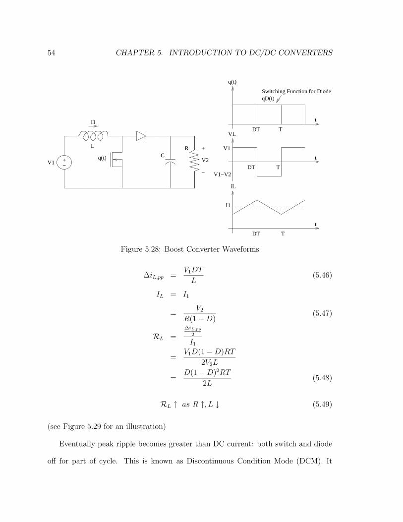
54 CHAPTER 5. INTRODUCTION TO DC/DC CONVERTERS
q(t)
Switching Function for Diode qD(t)
tI1 DT T
VL
L R +
+ −
Cq(t) V2V1
− V1−V2
iL
TDT
t
V1
I1
t
DT T
Figure 5.28: Boost Converter Waveforms
V1DT ΔiL,pp = (5.46)
L
IL = I1
V2 = (5.47)
R(1 − D) ΔiL,pp
2RL = I1
V1D(1 − D)RT =
2V2L D(1 − D)2RT
= (5.48) 2L
RL ↑ as R ↑, L ↓ (5.49)
(see Figure 5.29 for an illustration)
Eventually peak ripple becomes greater than DC current: both switch and diode
off for part of cycle. This is known as Discontinuous Condition Mode (DCM). It

55 5.2. DISCONTINUOUS CONDUCTION MODE
t
iL As R Increases
t
iL
DT T DT T
As L Decreases
Figure 5.29: Changing R and L
happens when RL > 1.
D(1 − D)2RT RL = 2L
RL
R
>
≥
1
2L (5.50)
D(1 − D)2T
At light load (big R and low power) we get DCM. Lighter load can be reached in
CCM for larger L. DCM occurs for:
L ≤ D(1 − D)2TR
(5.51) 2
The minimum inductance for CCM operation is sometimes called the “critical
inductance”.
D(1 − D)2TR LCRIT,BOOST = (5.52)
2
For some cases (e.g. we need to operate down to almost no load), this may be
unreasonably large.
Because of the new switch state, operating conditions are different (see Fig
ure 5.30).

56 CHAPTER 5. INTRODUCTION TO DC/DC CONVERTERS
q(t), qD(t)
VL DT
t
DCM
(D+D2)T T
V1
(D+D2)T t DT T
V1-V2
iL Must Be Zero in Remaining Time
t
DT (D+D2)T T
Figure 5.30: Different Operating Conditions
Voltage conversion ratio:
< VL > = 0 in P.S.S.
V1DT + (V1 − V2)D2T = 0
V1(D + D2) = V2D2
V2 D + D2 =
V1 D2
D = 1 + (5.53)
D2
where D2 < 1 − D.
How does this compare to CCM? In CCM:
V2 1 =
V1 1 − D

√
57 5.2. DISCONTINUOUS CONDUCTION MODE
1 − D + D =
1 − D D
= 1 + (5.54) 1 − D
Since V2 = 1 + D and D2 < 1 − D, V2 is bigger in DCM. V1 D2 V1
Eliminating D2 from equations, can be shown for boost:
V2 1 1 2D2RT = + 1 + (5.55)
V1 2 2 L
Therefore, conversion ratio depends on R, fsw, L, ... unlike CCM. This makes
control tricky, as all of our characteristics change for part of the load range.
How do we model DCM operation? Consider diode current (see Figure 5.31).
IL id
id
ipk
+ −
+ +
V2 id(t) V2V1
− −
I2
t
DT (D+D2)T T
Figure 5.31: DCM Operation Model
V1DT ipk =
L
D2T = Δt

58 CHAPTER 5. INTRODUCTION TO DC/DC CONVERTERS
Δi = L
V V1DT
= L L
V2 − V1
V1D D2 = (5.56)
V2 − V1
< iout > = < id >
1 1 = (D2T )(ipk)
2 T 1 V1 V1DT 1
= ( DT )( )2 V2 − V1 L T V 2TD2
= 1 (5.57) 2(V2 − V1)
Model as controlled current source as a function of D.
So DCM sometimes occurs under light load, as dictated by sizing of L.
• Sometimes we can not practically make L big enough.
• Must handle control (changes from CCM to DCM).
• Also, we get parasitic ringing in both switches (see Figure 5.32).
Vx
+ −
Ideal L Rings with Parasitic C’sV2 ++
V2 V1VxV1 − − t
DT D2T T
Figure 5.32: Parasitic Ringing
Sometimes people design to always be in DCM. Inductor size becomes very small
and we can get fast di (see Figure 5.33). dt

59 5.2. DISCONTINUOUS CONDUCTION MODE
CCM DCM
Desired i
V2
di/dt limited so cannot respond fast.
Figure 5.33: Design in DCM
In this case we get:
1. Very fast di capability. dt
2. Simple control model iout = f(D).
3. Small inductor size (EL minimized @ RL = 1)
But we must live with:
1. Parasitic ringing
2. High peak and RMS currents
3. Need additional filters
DCM is sometimes used when very fast response speed is needed (e.g. for voltage
regulator modules in microprocessors), especially if means are available to cancel
ripple (e.g. interleaving of multiple converters). In many other circumstances DCM
is avoided, though one may have to operate in DCM under light-load conditions to
keep component sizes acceptable.