5g enhanced mobile broadband radio interface on mmwave ......5g enhanced mobile broadband radio...
TRANSCRIPT

5G Enhanced Mobile Broadband Radio interface on mmWave – Hardware Architecture and role of Silicon Technologies
Dr. Anirban Bandyopadhyay, Director, RF Business Development, GLOBALFOUNDRIES, Inc., New York

Outline
Introduction to 5G
mmWave 5G Radio Access Technology Overview
mmWave 5G Radio Interface Architecture
1
2
3
Differentiated Silicon Technologies for mmWave 5G4
Summary & references5

Outline
Introduction to 5G
mmWave 5G Radio Access Technology Overview
mmWave 5G Radio Interface Architecture
1
2
3
Differentiated Silicon Technologies for mmWave 5G4
Summary & references5

What is 5G ?
5G is the next Generation cellular standard to support faster data rate, lower latency & more number of connected devices
2019+
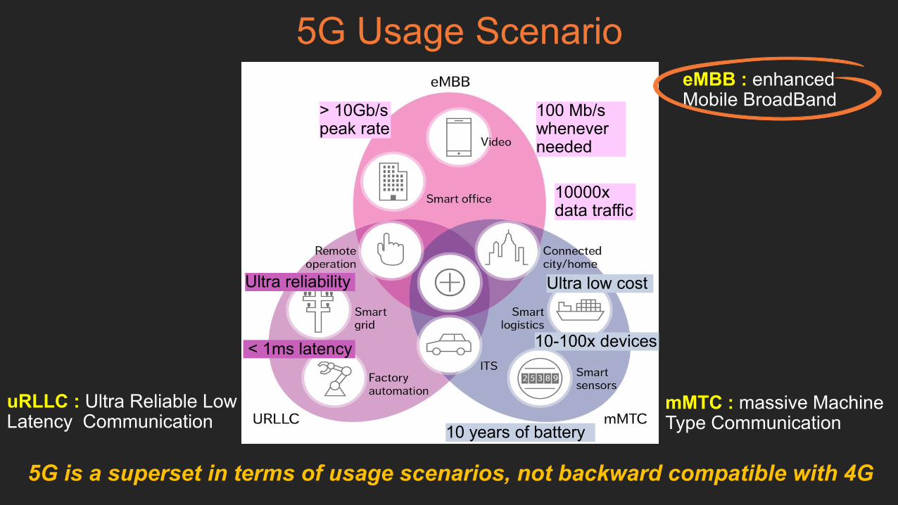
5G is a superset in terms of usage scenarios, not backward compatible with 4G
5G Usage Scenario
> 10Gb/s peak rate
100 Mb/s whenever needed
10000x data traffic
10-100x devices< 1ms latency
10 years of battery
Ultra low costUltra reliability
eMBB : enhanced Mobile BroadBand
uRLLC : Ultra Reliable Low Latency Communication
mMTC : massive Machine Type Communication

Data traffic density and higher data rate demand will always be on the rise
Do we really need 5G ?
• Cell edge coverage
• Peak & average data rate / throughput
Key Problems faced by current 4G connections
Concept of always being connectedremains a myth
Source: IWPC presentation, 2017

4G Frequency Bands
Bands are very fragmented with passband 20-200 MHz allocated among many carriers Max Channel Bandwidth 20MHz

Further enhancement in capacity/ peak data rate needs larger channel BW and/or higher Spectral Efficiency
Network Capacity Improvement
How good 4G can be ?
Carrier Aggregation(2X – 5X)
Downlink 100MHz (5 x 20MHz)Uplink 40MHz (2 x 20MHz)
Max. 20MHz Channel BW Higher Modulation level (16 QAM 256QAM)
Multiple Input Multiple Output (MIMO) Antenna
Downlink up to 256 QAM, 4X 4 MIMOUplink up to 64 QAM, 2x2 MIMO
Downlink Theoretical max data rate ~2 Gb/s (using 5X CA, 256 QAM & 4x4 MIMO

Outline
Introduction to 5G
mmWave 5G Radio Access Technology Overview
mmWave 5G Radio Interface Architecture
1
2
3
Differentiated Silicon Technologies for mmWave 5G4
Summary & references5

5G will have both sub 6GHz & mmWave Bands
Enhanced
Mobile
Broadband
Sub 6 GHz 5G4x4 DL MIMO
Conventional + mMIMO BTS
mmWave 5G
mMIMO+ Phased Arrays BTS
Phased arrays
New Bands + Re-farmed 4G Bands
FR1 Sub 6GHz & FR2 24 – 52 GHz defined so far (3GPP Rel 15)
Rel 16 will define bands > 52GHz

11
• Contiguous Spectrum availability
- much more than sub 6GHz
Higher Channel bandwidth (defined up to 400MHz, can be more) and hence data rate
• High frequency / small wavelength- Smaller antenna, makes large arrays
possible
Highly directive beam enables spatial multiplexing (spectral efficiency)
Less interference and more efficient use of Tx/ Rx power
• High link loss
- Atmospheric, Rain, foliage, building material absorption
Distance between Access point & UserEquipment (UE) has to be small (< 100-200m)
Why mmWave?
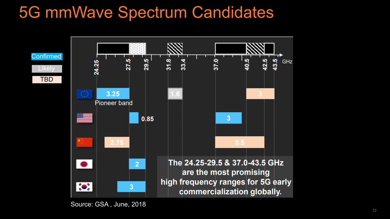
5G mmWave Spectrum Candidates
12
Confirmed
Likely
TBD
Source: GSA , June, 2018
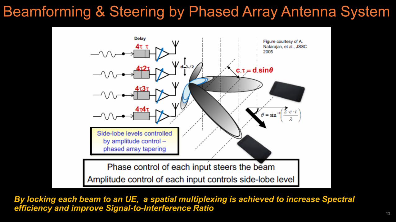
Beamforming & Steering by Phased Array Antenna System
By locking each beam to an UE, a spatial multiplexing is achieved to increase Spectral efficiency and improve Signal-to-Interference Ratio
13

4G vs mmWave 5G Radio Access Network (RAN)
Source: Mitsubishi Electric
mmWave enables excellent spatial selectivity and hence high spectral efficiency & low interference

Capacity Improvement using mmWave 5G
15
Channel BW 50-400MHz
(4G max. 100MHz using 5X CA)
Spatial Multiplexing using Beamforming (8-16 Beams)
(4G 4x4 MIMO provides 4 data streams)
At least 5-10X of 4G
~10-20Gb/s
Might use lesser order Modulation to start with (64QAM instead of 4G 256QAM)

Timeline for 5G deployment
16
mmWave-based enhanced mobile broadband in UE will be widespread
during phase 2 of 5G launch
Rel. 15 Rel. 16 Rel. 17
2017 2018 2019 2020 2021 2022
Sub 6GHz & 24-52 GHz
3GPP
Phase 1 Commercial Launches
5GNR
Mainly sub 6 GHz 5G &
mmWave fixed wireless +mmWave
eMBB
Phase 2 Commercial Launches
Non-
standalone
(NSA)
Standalone
(SA) V2X, IoT & others
52-100 GHz
eMBB

Outline
Introduction to 5G
mmWave 5G Radio Access Technology Overview
mmWave 5G Radio Interface Architecture
1
2
3
Differentiated Silicon Technologies for mmWave 5G4
Summary & references5

Current Cellular Radio Interface Architecture
18
Modem
Filters/ Duplexers
Power AmplifiersSwitch Single Chip Solution
Up/Dn Converter + LO’s
LNAs
Filters
• Today’s most high tier LTE handsets have LNA’s in RFFE to increase Rx sensitivity
• Transceiver is a single-chip solution currently most system on 28nm, QTI has 14FF based transceiver for higher CAT (16+) 4G handsets
• CAT 16+ 4G (and sub 6GHz 5G) Handsets will need many LO generators to support 4x4 MIMO, high order CA
Source: based on block diagram from http://www.anandtech.com/show/6541/
RF
Zero or low IF
Baseband Processor
ADC
DAC
Digital signal
Digital signalZero or low IF
RF
RF

Different Beamforming Architectures
© 2017 GLOBALFOUNDRIES19
Digital / Digital Beamforming
Analog Beamforming
Hybrid Beamforming
Combiner / Splitter
Modem + Host Processor
• Smallest #components• Lowest power dissipation• Complexity in phase shifting• Interference rejection (signal
synthesized in power combiner before mixer)
• Large # components• Higher power dissipation• Rx chains see spatial
interference (requires high dynamic range)
• Simple to implement
• For large arrays where analog & digital beamforming are inefficient and complex
EIRP, Rx sensitivity, available form factor, power budget determine array size and beamforming architecture for a particular mmWave application
SPDT
LNA
PA
LNA
PA
/2
/2
SPDT
Modem + Host Processor
Phase & Amplitude control
Up/DownConv
ADC/DACPower Combiner/Splitter
SPDT
LNA
PA
LNA
PA
/2
/2
SPDT
Digital Phase Shifter
Phase & Amplitude control
Up/DownConv ADC/DAC
Power Combiner/splitter
ADC/DAC
/2
/2
SPDT
SPDT
LNA
PA
LNA
PA
Up/Down conv Combiner
/ Splitter
Digital Phase shifter Modem + Host
Processor ADC/DACUp/Down
conv
Digital Phase shifter
SPDT
LNA
PA
LNA
PA
/2
/2
SPDT
Digital Phase Shifter
Phase & Amplitude control
Up/DownConv
ADC/DACPower Combiner/ splitter
Phase/amplitude controllermmWave
IF Digital signal

Transmission Lines Loss: Distance to Ground Plane
• Transmission line loss increases with frequency
- Skin effect
- Eddy current loss in substrate
• Thick Top metals (more than skin depth)
• Ground plane in BEOL prevents fields from entering substrate
• Distance from Ground Plane helps
• Higher substrate resistivity up to a level (~200Ohm-cm) helps
20
Source: Prof. Gabriel Rebeiz, UCSD on 90nm SiGe
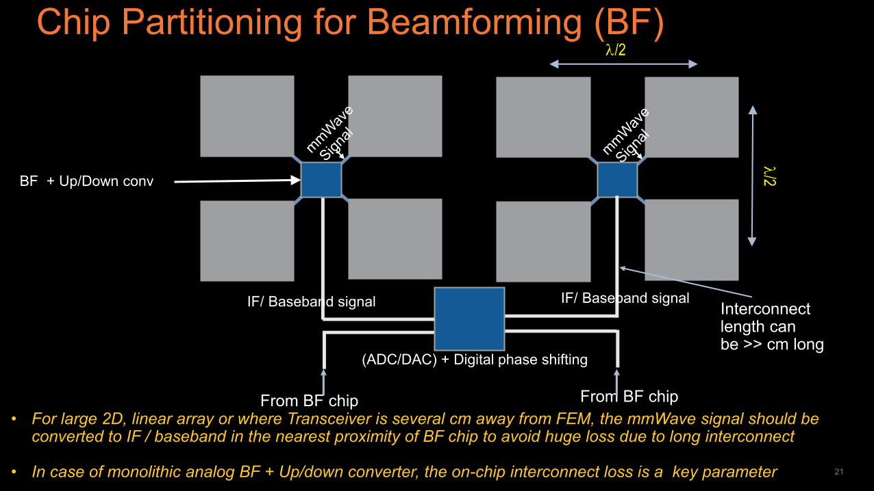
Chip Partitioning for Beamforming (BF)
21
• For large 2D, linear array or where Transceiver is several cm away from FEM, the mmWave signal should be converted to IF / baseband in the nearest proximity of BF chip to avoid huge loss due to long interconnect
• In case of monolithic analog BF + Up/down converter, the on-chip interconnect loss is a key parameter
From BF chip
BF + Up/Down conv
(ADC/DAC) + Digital phase shifting
IF/ Baseband signal
/2
/2
IF/ Baseband signal Interconnect length can be >> cm long
From BF chip

Outline
Introduction to 5G
mmWave 5G Radio Access Technology Overview
mmWave 5G Radio Interface Architecture
1
2
3
Differentiated Silicon Technologies for mmWave 5G4
Summary & references5

EIRP Definition
23
Equivalent Isotropic Radiated Power
(EIRP) is the product of transmitter power and the
antenna gain in a given direction relative to an
isotropic antenna of a radio transmitter.
It is the power that an isotropic (omnidirectional)
antenna would have to transmit to match the
directional reception
Normally the EIRP is given in dBi, or decibels over
isotropic.

Impact of Semiconductor Technology on Array Size
24
Technology with better Rx noise figure and higher per element Tx power output will need fewer array elements for a target Rx antenna G/T and Tx antenna EIRP, respectively
NF = 1.5 dB
NF = 4.5 dB
NF = 2.5 dB
NF = 3.5 dB
50 mW
5 mW
20 mW
10 mW
Technology with better FOM smaller array LOWER COST & AREA
* Courtesy of Anokiwave, “Highly Integrated Silicon ASICs – A Disruptive Technology for AESAs”, Ian Gresham and Dave Corman, Sep 30, 2015 WebinarSource: Anokiwave webinar

EIRP Example IBM/Ericsson 28GHz 64-Element Phased Array in 130nm SiGe (8HP)
25

26
Silicon Technologies for mmWave 5G Radio InterfaceTechnology Key Features Device Cross-Section
RF CMOS (65nm - 28nm)
• High-volume logic process technology base with multiple foundries
• Comprehensive IP offerings for System-on-Chip (SOC)• Traction in mmWave markets: WiGig 802.11ad (60GHz),
77GHz auto radar
PD-SOI (45nm)
PD-SOI = Partially Depleted Silicon on Insulator• High-speed w/ lower junction capacitance, isolation &
stacking• 180nm RF SOI extensively used in cellular & Wi-Fi FEM• Early adoption in 5G & Sat Comm for 45nm PDSOI with
highest Ft/Fmax & optimum BEOL stack
FD-SOI (28nm - 22nm)
FD-SOI = Fully Depleted Silicon-on-Insulator• Delivers FinFET-like performance and power-efficiency at
28/22nm cost• Transistor body-biasing for flexible trade-off between
performance and power• Enables applications across mobile, IoT and mmWave markets
SiGe (130nm -90nm)
SiGe = Silicon Germanium• Based on higher performance & power tolerant HBT ( vs FET)• Technology optimized for micro and mmWave
applications: backhaul, E-band links, Sat Comm, automotive radar, A&D
GS D
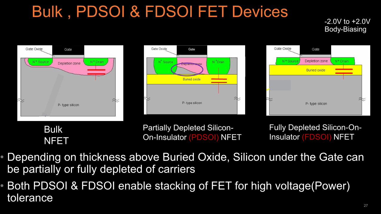
Bulk , PDSOI & FDSOI FET Devices-2.0V to +2.0VBody-Biasing
27
Leakage P
ow
er
• Depending on thickness above Buried Oxide, Silicon under the Gate can be partially or fully depleted of carriers
• Both PDSOI & FDSOI enable stacking of FET for high voltage(Power) tolerance
Bulk
NFET
Partially Depleted Silicon-
On-Insulator (PDSOI) NFET
Fully Depleted Silicon-On-
Insulator (FDSOI) NFET

Essential Elements for a Silicon Technology for mmWave
• High-performance technology
– Higher performance enables design flexibility & techniques for a more robust design
– fT / fMAX should be at a minimum 3x and preferably > 5x application frequency
– RF FOMs (Self Gain, Gain efficiency, Ft/Fmax, Nfmin, 1/f noise) appropriate for target mmWave applications
• Low loss BEOL (metal and dielectric stack)
– Thick top metal(s)
– Distance to substrate
– Substrate resistivity
• Well-modeled (including EM simulation) mmWave technology
– mmWave model-to-hardware correlation is key to minimize design iterations
• Reliability and Ruggedness – Devices and components proven reliable and rugged over the voltage, temperature ranges
28

PA Efficiency increases with Input power level
PA linearity requirement and signal PAPR for the application determine the operating point back off from saturation
PA Efficiency at operating point matters
Power Amplifier – Psat, P1dB, Efficiency
Input Power
Ou
tpu
t P
ow
er
PA
Effic
ien
cy
0.05
0.15
0.25
0.35
0.55
0.45
Class AB
Class A
Saturation (Psat)
Saturation (Psat)
PAPR (peak-to-average power ratio)
1dB
P1dB

45RFSOI BEOL Is Optimized to Provide Benefits for Millimeter Wave Operation Increased ‘d’ to
substrate reduces parasitics / coupling
2 High resistivity trap rich substrate:
– Improves back-end-of-line (BEOL) losses due to parasitics (~0.8dB reduction in TL IL per mm @ 28 GHz)
– Reduces harmonics due to trap rich substrate for improved linearity
11LM 8LM
AL
Cu
Cu
AL
Cu
Cu
Cu
d
1 Raised thick Cu levels:
– High Q inductors and transformers
– Low loss transmission lines
– High Q MIMs; high density MIMs or APMOMs
– Dual thick Cu levels provide design flexibility
BEOL IL comparison with different substrates30

45RFSOI : High Performance mmWave Switches
Number
of stacks
IL @ 28/50 GHz
(dB) W/Open
Iso @ 28/50 GHz
(dB) W/Open
IP1dB (dBm)
at 14 GHz
IIP3 (dBm)
at 14 GHz
3 0.76/1.17 23.91/17.06 30 49.5
4 0.91/1.18 24.14/17.94 32 48.7
5 0.98/1.13 24.81/19.16 33 48.4
• RonCoff ~90 fS
• 28 GHz SPDT 3 stack
– IL 0.76 dB
– Iso: 23 dB
– Pmax: 23 dBm
– One tone IIP3 49.5 dBm
• HR substrate provides improved parasitics over bulk
Measured Ron versus Frequency
Measured SPDT IL versus Frequency
31Source: Globalfoundries test results

45RFSOI differentiated silicon results: 23dBm Psat@42% PAEmax
32
28 GHz LNA/PA/switch silicon results
PA PAE at Psat Psat Gain
GF Single ended PA 41.5% 16.2 dBm 13 dB
Differential PA** (26 GHz) 42% 23 dBm 21 dB
Differential PA** (26 GHz) 37% 22.2 dBm 21 dB
LNA Gain IIP3 NF
GF Reference 45RFSOI
designs 13 dB 4.3 dBm 1.3 dB
SwitchInsertion
LossIsolation OIP3
GF Reference 45RFSOI
designs (RonCoff = 90 fs, 1 V)0.65 dB 26 dB 46 dBm
Silicon Verified Results
** Georgia Tech
Psat: 22.5dBm,
PAEmax: 43%

High Fmax
High mmWave self
gain
Low mmWave
noise
“mmWave FET stacking“
enables single chip mmWave integration
22FDX® Technology: Optimized for mmWave SoC
1.2X > 28 nm 2.5x > 28 nm NFmin < 28nm Single stage PA Pout >> 28 nm ormuch smaller die area for same EIRP
Low Power, High Density Logic Integration (Forward & Reverse Body Bias)
-2V to +2V
Body-Biasing
17

22FDX Enables Lowest Power Consumption for mmWave Applications
0.0E+00
5.0E+11
1.0E+12
1.5E+12
2.0E+12
2.5E+12
3.0E+12
1.E-03 1.E-01 1.E+01 1.E+03
ft*g
m/I
(H
z/V
)
I/w (uA/um)
Ft*gm/I
22FDX
14LPP
28SLP
34
0.0E+00
5.0E+11
1.0E+12
1.5E+12
2.0E+12
2.5E+12
3.0E+12
3.5E+12
4.0E+12
1.E-03 1.E-01 1.E+01 1.E+03
fmax
*gm
/I (
Hz/
V)
I/w (uA/um)
Fmax*gm/I
22FDX
14LPP
28SLP
For mmWave LNA, mixer circuits, 22FDX has 30% higher performance and 16% lower current than 28nm
For mmWave PA circuits, 22FDX far outperforms any other CMOS node
Source: Globalfoundries test results

22FDX® based 5G 28 GHz differential PA
35
High efficiency, high gain amplification
Parameters Measured Measured
Stacking 3-Stack PA 2-Stack PA
S21 peak freq (GHz) 27.8 29
IDDQ (mA) 15.9 15.8
Gain (dB) 12.4 12.7
P1dB (dBm) 17.4 15.8
Psat/P3dB (dBm) 18.2 16.4
PAE_Psat-6dB (%) 18.3 20.8
PAE_peak (%) 30.2 41.0
S11 -10.6 -9.9
S22 -2.1 -1.2
Ruggedness Passed 18 dBm 15 dBm
MPW2217 PA (2-Stack) Schematic
• All designs metal stack # 11• Ruggedness stress tested at VSWR 5:1; Tests ongoing
PA is the fulcrum around which 5G architecture revolves and 22FDX enables BIC PA performance for Integrated RF SOC
Source: Globalfoundries test results

Measured switch & LNA performance on 22FDX®
36
3-stacked switch architecture with power handling up to 23 dBm @ 4:1 VSWR
Freq. 28 GHz 40 GHz
S21 (dB) -0.95 -1.25
S11 (dB) -13 -11
S21 (dB) OFF -25.3 -21.5
IIP3 (dBm) 45 44
VD
D
V
G
1
N
0
N
1V
G
0
OU
T
IN
V
B1
Lg
Ls
Ld
C
c
External
Bias
Choke
22FDX® mmWave FETs• <10 mW power consumption
• NF 2.6 dB @ 28 GHz in 1st generation
• NF <2 dB @ 28 GHz in 2nd gen
5G mmWave switches based on mmWave layouts with increased gate pitch are targeted to have ~ 0.6-0.7 dB insertion loss at 28 GHz and better power handling due to low capacitances
5G mmWave switches based on mmWave layouts with increased gate pitch are targeted to have ~ 0.6-0.7 dB insertion loss at 28 GHz and better power handling due to low capacitances
“Beats Best GaAs pHEMT LNAs” Prof. Gabriel Rebeiz, UCSD
“Beats Best GaAs pHEMT LNAs” Prof. Gabriel Rebeiz, UCSD
Source: Globalfoundries test results

• GF continues to push scaling of SiGe HBTs
• Optimizing vertical (intrinsic) & lateral (extrinsic) profiles allows one to gain Ft – BV margin
37
SiGe (P) Base
Regions to optimize for breakdown
Breakdown limits set by avalanche, tunneling, or base punch-through as transistors are scaled for high Ft
8HP
9HP
Avoids the need for multi-stacking approach used for FETs improves PAE for PA
SiGe HBT Breakdown (BVcbo) Saturating at 4 V for Ft >500 GHz
Source: GLOBALFOUNDRIES

130nm & 90nm SiGe Technologies - HBT’s offer High Ft/Fmax at low power
• SiGe (8XP) offers Fmax of 350 GHz; SiGe (9HP) offers Fmax of 370 GHz
• CMOS logic supporting thin and thick oxide for 1.2 V / 1.5 V, 1.8 V / 2.5 V / 3.3 V
• Thick top level metals for improved transmission line loss
38
Fmax
Ft
Source: GLOBALFOUNDRIES
High Fmax and breakdown voltage of SiGe makes it an ideal technology for
high Psat, Gain, PAE, & linearity of PA with high reliability.

39
SiGe8HP/8XP PA for Psat > 23dBm

Generic architecture : mmWave 5G radio interface for UE–chip partitioning options
40
Chip partitioning & technology adoption will depend on Tx power, power efficiency, cost and available
form factor
TransceiverFEM subsystemAntenna
Subsystem
Example of digital beamforming shown, can be analog
beamforming as well
Modem / Digital Phase
splitter / power
combiner
Application Processor
RF & IF up/down conversion
LNA
PA
SPDT
LNA
PA
SPDT RF & IF up/down conversion
ADC/DAC
ADC/DAC
Baseband and Application Processing
14/12/10 nm FinFET
22FDX®
45RFSOI up to IF
28/22 nm bulk CMOS w/ SiGe/III-V PA & RF SOI switch if needed
28/22 nm bulk45RFSOI up to IF
14/10/7 nm FinFET
Possible chip
partitioning options
14/10/7 nm FinFET
14/10/7 nm FinFET
14/10/7 nm FinFET

Chip partitioning option: radio interface for mmWave 5G infrastructure
41
Technology solution will be determined by TX power, #arrays (system cost) & system power dissipation
Possible chip
partitioning
options
SiGe or 45RFSOI 14/10/7 nm FinFET 14/10/7 nm FinFET
22FDX®
BB
L1/L2/L3
Data
Conv
Subsystem
Transceiver
Subsystem
FEM
Subsystem
Antenna
Subsystem
DFE
DPD/DUC/
DDC/CFR
Digital UnitRadio Unit
Hybrid Beam FormingLNA
PA
SPDTPower
comb/splitters and ph shifters
LNA
PA
LNA
PA
LNA
PA
Power comb/splitters and ph shifters
DFE L1/L2/L3 Baseband Processing
DAC/ADC
SPDT
SPDT
SPDT
14/10/7 nm FinFET
planar bulk CMOS w/ SiGe/III-V PA & RF SOI switch, if needed
14/10/7 nm FinFET
14/10/7 nm FinFET
DAC/ADC
DAC/ADC
DAC/ADC
Up/Dn conv
Up/Dn conv

Comparison of 22FDX® and 28 nm for beamforming
42
Analysis for 16QAM UL/DL, 100MHz RF BW
Analog Beamforming (ABF) Digital Beamforming (DBF)
~20% reduction in power dissipation w.r.t. 28 nm bulk for analog high IF beamforming,
The power advantage of 22FDX is even better for digital beamforming
Technology 28 nm HKM 22 nm FD-SOI
ArchitectureABF, High IF,
N=8
ABF, High IF,
N=8
DBF, DC,
N=8
ABF, High IF,
N=4
DBF, DC,
N=4
PA Pout (dBm) 7 7 7 13 13
Pdc (mW)
(Tx/RX 0.3/0.7)506 415 360 315 289
All 22 nm
FD-SOI power
consumption results
based on measured
results of silicon
blocks
Source: Globalfoundries presentation at IMS 2018 workshop

Outline
Introduction to 5G
mmWave 5G Radio Access Technology Overview
mmWave 5G Radio Interface Architecture
1
2
3
Differentiated Silicon Technologies for mmWave 5G4
Summary & references5

Summary
44
We have covered the enhanced Mobile Broadband (eMBB) usage scenario of 5G
The use of mmWave carrier frequency will enable large channel bandwidth and high spectral efficiency
The phased array technique to be used for mmWave 5G will enable Silicon technologies to play key roles in mmWave 5G systems
We highlighted partially depleted (PD) and fully depleted (FD) SOI technologies along with SiGe BiCMOS technologies as differentiated Silicon technology choices for mmWave 5G radio interface.

References
45
https://www.qualcomm.com/media/documents/files/making-5g-nr-a-commercial-reality.pdf
https://www.globalfoundries.com/tech-resources/document-center
https://www.etsi.org/technologies-clusters/technologies/5g
https://spectrum.ieee.org/static/the-race-to-5g
https://www.ericsson.com/en/white-papers/advanced-antenna-systems-for-5g-networks
http://www.microwavejournal.com/blogs/25-5g/post/30882-g-is-coming-what-to-expect-and-why
https://ims2018.org/technical-program/workshops-and-short-courses#2018-06-15
Please feel free to contact me at [email protected] with any questions or follow up