512 kbit / 1 mbit / 2 mbit / 4mbit 1.8v spi serial flash
TRANSCRIPT
Data Sheet
FEATURES:
• Single Voltage Read and Write Operations– 1.65-1.95V
• Serial Interface Architecture– SPI Compatible: Mode 0 and Mode 3
• High Speed Clock Frequency– 40MHz
• Superior Reliability– Endurance: 100,000 Cycles– Greater than 100 years Data Retention
• Ultra-Low Power Consumption:– Active Read Current: 2 mA (typical @ 20MHz)– Standby Current: 2 µA (typical)
• Flexible Erase Capability– Uniform 4 KByte sectors– Uniform 32 KByte overlay blocks– Uniform 64 KByte overlay blocks
(2 Mbit and 4 Mbit only)• Fast Erase and Byte-Program:
– Chip-Erase Time: 125 ms (typical)– Sector-/Block-Erase Time: 62ms (typical)– Byte-Program Time: 50 µS (typical)
• Auto Address Increment (AAI) Programming– Decrease total chip programming time over
Byte-Program operations• End-of-Write Detection
– Software polling the BUSY bit in Status Register– Busy Status readout on SO pin
• Reset Pin (RST#) or Programmable Hold Pin (HOLD#) option– Hardware Reset pin as default– Hold pin option to suspend a serial sequence
without deselecting the device• Write Protection (WP#)
– Enables/Disables the Lock-Down function of the status register
• Software Write Protection– Write protection through Block-Protection bits in
status register• Temperature Range
– Industrial: -40°C to +85°C• Packages Available
– 8-lead SOIC (150 mils)– 8-contact WSON (5mm x 6mm)
• All non-Pb (lead-free) devices are RoHS compliant
512 Kbit / 1 Mbit / 2 Mbit / 4Mbit 1.8V SPI Serial FlashSST25WF512 / SST25WF010 / SST25WF020 / SST25WF040
SST25VF016B16Mb Serial Peripheral Interface (SPI) flash memory
PRODUCT DESCRIPTION
The SST25WF512, SST25WF010, SST25WF020, andSST25WF040 are members of the Serial Flash 25 Seriesfamily and feature a four-wire, SPI-compatible interface thatallows for a low pin-count package which occupies lessboard space and ultimately lowers total system costs.SST25WF512/010/020/040 SPI serial flash memories aremanufactured with SST proprietary, high-performanceCMOS SuperFlash technology. The split-gate cell designand thick-oxide tunneling injector attain better reliability andmanufacturability compared with alternate approaches.
The SST25WF512/010/020/040 devices significantlyimprove performance and reliability, while lowering powerconsumption. The devices write (Program or Erase) with a
single power supply of 1.65-1.95V for SST25WF512/010/020/040. The total energy consumed is a function of theapplied voltage, current, and time of application. Since forany given voltage range, the SuperFlash technology usesless current to program and has a shorter erase time, thetotal energy consumed during any Erase or Program oper-ation is less than alternative flash memory technologies.
The SST25WF512/010/020/040 devices are offered inboth 8-lead SOIC and an 8-contact WSON packages. SeeFigure 2 for the pin assignment.
©2009 Silicon Storage Technology, Inc.S71328-08-000 11/091
The SST logo and SuperFlash are registered Trademarks of Silicon Storage Technology, Inc.These specifications are subject to change without notice.
Data Sheet
512 Kbit / 1 Mbit / 2 Mbit / 4 Mbit 1.8V SPI Serial FlashSST25WF512 / SST25WF010 / SST25WF020 / SST25WF040
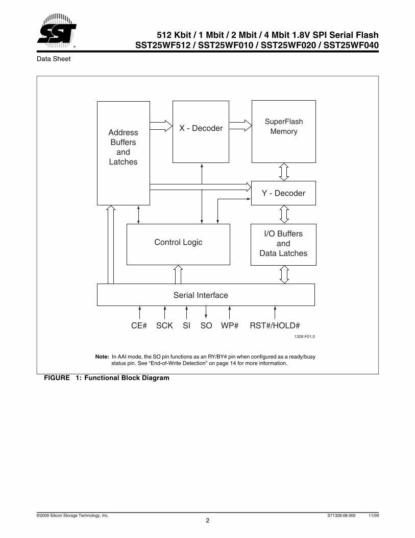
FIGURE 1: Functional Block Diagram
1328 F01.0
I/O Buffersand
Data Latches
SuperFlashMemoryX - Decoder
Control Logic
AddressBuffers
andLatches
CE#
Y - Decoder
SCK SI SO WP# RST#/HOLD#
Serial Interface
Note: In AAI mode, the SO pin functions as an RY/BY# pin when configured as a ready/busy status pin. See “End-of-Write Detection” on page 14 for more information.
2©2009 Silicon Storage Technology, Inc. S71328-08-000 11/09
Data Sheet
512 Kbit / 1 Mbit / 2 Mbit / 4 Mbit 1.8V SPI Serial FlashSST25WF512 / SST25WF010 / SST25WF020 / SST25WF040
PIN DESCRIPTION
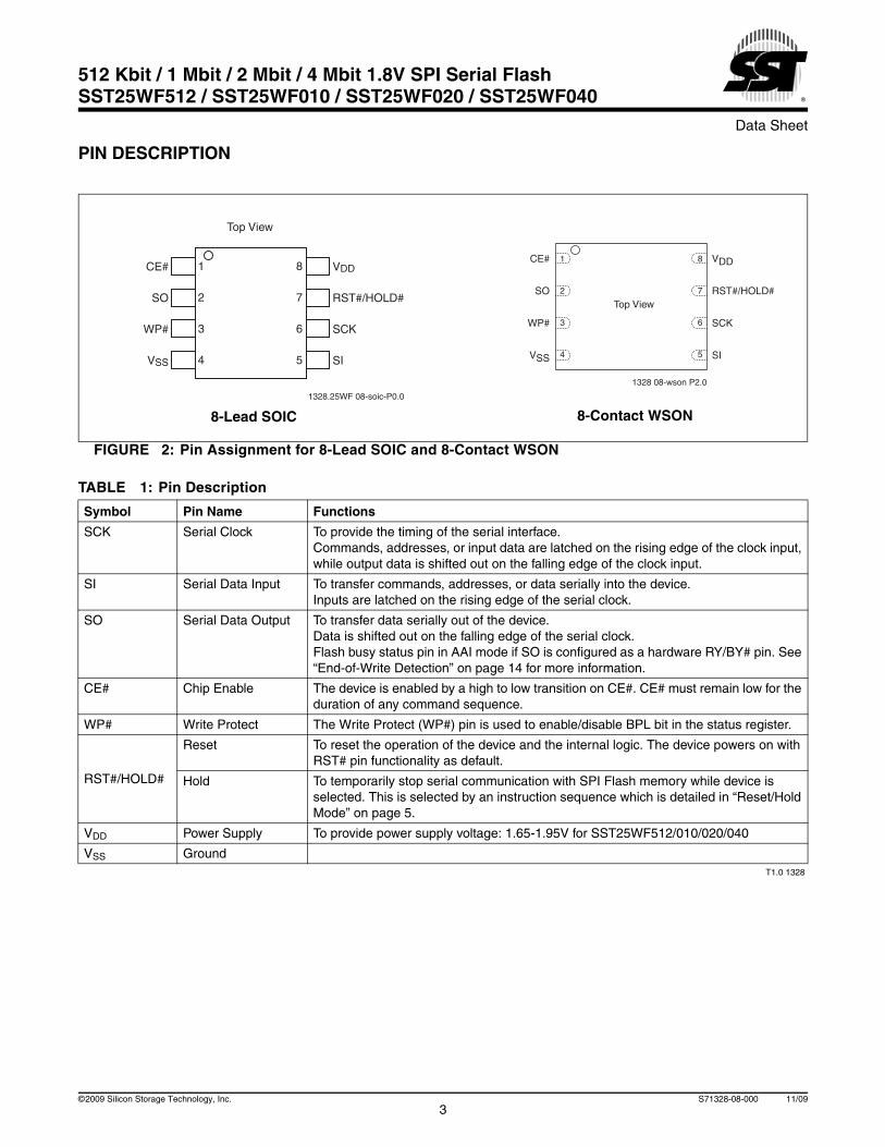
FIGURE 2: Pin Assignment for 8-Lead SOIC and 8-Contact WSON
TABLE 1: Pin Description
Symbol Pin Name Functions
SCK Serial Clock To provide the timing of the serial interface.Commands, addresses, or input data are latched on the rising edge of the clock input, while output data is shifted out on the falling edge of the clock input.
SI Serial Data Input To transfer commands, addresses, or data serially into the device.Inputs are latched on the rising edge of the serial clock.
SO Serial Data Output To transfer data serially out of the device.Data is shifted out on the falling edge of the serial clock.Flash busy status pin in AAI mode if SO is configured as a hardware RY/BY# pin. See “End-of-Write Detection” on page 14 for more information.
CE# Chip Enable The device is enabled by a high to low transition on CE#. CE# must remain low for the duration of any command sequence.
WP# Write Protect The Write Protect (WP#) pin is used to enable/disable BPL bit in the status register.
RST#/HOLD#
Reset To reset the operation of the device and the internal logic. The device powers on with RST# pin functionality as default.
Hold To temporarily stop serial communication with SPI Flash memory while device is selected. This is selected by an instruction sequence which is detailed in “Reset/Hold Mode” on page 5.
VDD Power Supply To provide power supply voltage: 1.65-1.95V for SST25WF512/010/020/040
VSS GroundT1.0 1328
1
2
3
4
8
7
6
5
CE#
SO
WP#
VSS
VDD
RST#/HOLD#
SCK
SI
Top View
1328.25WF 08-soic-P0.0
1
2
3
4
8
7
6
5
CE#
SO
WP#
VSS
Top View
VDD
RST#/HOLD#
SCK
SI
1328 08-wson P2.0
8-Lead SOIC 8-Contact WSON
3©2009 Silicon Storage Technology, Inc. S71328-08-000 11/09
Data Sheet
512 Kbit / 1 Mbit / 2 Mbit / 4 Mbit 1.8V SPI Serial FlashSST25WF512 / SST25WF010 / SST25WF020 / SST25WF040
MEMORY ORGANIZATION
The SST25WF512/010/020/040 SuperFlash memoryarrays are organized in uniform 4 KByte with 16 KByte, 32KByte, and 64 KByte (2 Mbit and 4 Mbit Only) overlay eras-able blocks.
DEVICE OPERATION
The SST25WF512/010/020/040 are accessed throughthe SPI (Serial Peripheral Interface) bus compatible proto-col. The SPI bus consist of four control lines; Chip Enable
(CE#) is used to select the device, and data is accessedthrough the Serial Data Input (SI), Serial Data Output (SO),and Serial Clock (SCK).
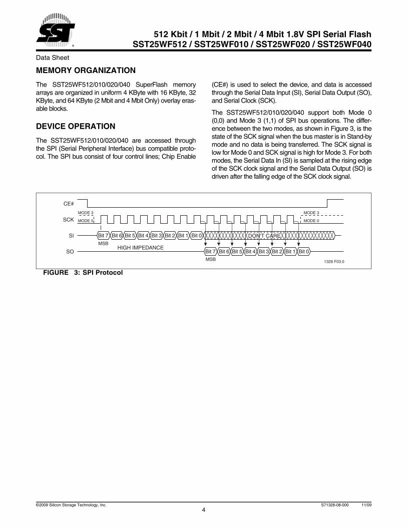
The SST25WF512/010/020/040 support both Mode 0(0,0) and Mode 3 (1,1) of SPI bus operations. The differ-ence between the two modes, as shown in Figure 3, is thestate of the SCK signal when the bus master is in Stand-bymode and no data is being transferred. The SCK signal islow for Mode 0 and SCK signal is high for Mode 3. For bothmodes, the Serial Data In (SI) is sampled at the rising edgeof the SCK clock signal and the Serial Data Output (SO) isdriven after the falling edge of the SCK clock signal.
FIGURE 3: SPI Protocol
1328 F03.0
MODE 3
SCK
SI
SO
CE#
MODE 3
DON'T CARE
Bit 7 Bit 6 Bit 5 Bit 4 Bit 3 Bit 2 Bit 1 Bit 0
Bit 7 Bit 6 Bit 5 Bit 4 Bit 3 Bit 2 Bit 1 Bit 0
MODE 0MODE 0
HIGH IMPEDANCEMSB
MSB
4©2009 Silicon Storage Technology, Inc. S71328-08-000 11/09
Data Sheet
512 Kbit / 1 Mbit / 2 Mbit / 4 Mbit 1.8V SPI Serial FlashSST25WF512 / SST25WF010 / SST25WF020 / SST25WF040
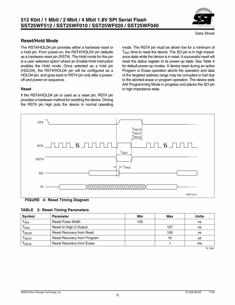
Reset/Hold ModeThe RST#/HOLD# pin provides either a hardware reset ora hold pin. From power-on, the RST#/HOLD# pin defaultsas a hardware reset pin (RST#). The Hold mode for this pinis a user selected option where an Enable-Hold instructionenables the Hold mode. Once selected as a hold pin(HOLD#), the RST#/HOLD# pin will be configured as aHOLD# pin, and goes back to RST# pin only after a power-off and power-on sequence.
Reset
If the RST#/HOLD# pin is used as a reset pin, RST# pinprovides a hardware method for resetting the device. Drivingthe RST# pin high puts the device in normal operating
mode. The RST# pin must be driven low for a minimum ofTRST time to reset the device. The SO pin is in high imped-ance state while the device is in reset. A successful reset willreset the status register to its power-up state. See Table 4for default power-up modes. A device reset during an activeProgram or Erase operation aborts the operation and dataof the targeted address range may be corrupted or lost dueto the aborted erase or program operation. The device exitsAAI Programming Mode in progress and places the SO pinin high impedance state.
FIGURE 4: Reset Timing Diagram
TABLE 2: Reset Timing Parameters
Symbol Parameter Min Max Units
TRST Reset Pulse Width 100 ns
TRHZ Reset to High-Z Output 107 ns
TRECR Reset Recovery from Read 100 ns
TRECP Reset Recovery from Program 10 µs
TRECE Reset Recovery from Erase 1 msT2.1328
1328 Fx4.0
CE#
SO
SI
SCK
RST#
TRECRTRECPTRECE
TRST
TRHZ
5©2009 Silicon Storage Technology, Inc. S71328-08-000 11/09

Data Sheet
512 Kbit / 1 Mbit / 2 Mbit / 4 Mbit 1.8V SPI Serial FlashSST25WF512 / SST25WF010 / SST25WF020 / SST25WF040
Hold
The Hold operation enables the hold pin functionality of theRST#/HOLD# pin. Once set to hold pin mode, the RST#/HOLD# pin continues functioning as a hold pin until thedevice is powered off and then powered on. After a power-off and power-on, the pin functionality returns to a reset pin(RST#) mode. See “Enable-Hold (EHLD)” on page 20 fordetailed timing of the Hold instruction.
In the hold mode, serial sequences underway with the SPIFlash memory are paused without resetting the clockingsequence. To activate the HOLD# mode, CE# must be inactive low state. The HOLD# mode begins when the SCKactive low state coincides with the falling edge of theHOLD# signal. The Hold mode ends when the rising edgeof the HOLD# signal coincides with the SCK active lowstate. If the falling edge of the HOLD# signal does not coin-cide with the SCK active low state, then the device enters
Hold mode when the SCK next reaches the active lowstate. Similarly, if the rising edge of the HOLD# signal doesnot coincide with the SCK active low state, then the deviceexits Hold mode when the SCK next reaches the active lowstate. See Figure 5 for Hold Condition waveform.
Once the device enters Hold mode, SO will be in high-impedance state while SI and SCK can be VIL or VIH.
If CE# is driven active high during a Hold condition, thedevice returns to standby mode. The device can then bere-initiated with the command sequences listed in Tables 9and 10. As long as HOLD# signal is low, the memoryremains in the Hold condition. To resume communicationwith the device, HOLD# must be driven active high, andCE# must be driven active low. See Figure 5 for Hold tim-ing.
FIGURE 5: Hold Condition Waveform
Write ProtectionSST25WF512/010/020/040 provide software Write pro-tection. The Write Protect pin (WP#) enables or disablesthe lock-down function of the status register. The Block-Protection bits (BP2, BP1, BP0, and BPL) in the status reg-ister provide Write protection to the memory array and thestatus register. See Table 5 for the Block-Protectiondescription.
Write Protect Pin (WP#)
The Write Protect (WP#) pin enables the lock-down func-tion of the BPL bit (bit 7) in the status register. When WP#is driven low, the execution of the Write-Status-Register(WRSR) instruction is determined by the value of the BPLbit (see Table 3). When WP# is high, the lock-down func-tion of the BPL bit is disabled.
Active Hold Active Hold Active
1328 Fx5.0
SCK
HOLD#
TABLE 3: Conditions to execute Write-Status-Register (WRSR) Instruction
WP# BPL Execute WRSR Instruction
L 1 Not Allowed
L 0 Allowed
H X AllowedT3.0 1328
6©2009 Silicon Storage Technology, Inc. S71328-08-000 11/09
Data Sheet
512 Kbit / 1 Mbit / 2 Mbit / 4 Mbit 1.8V SPI Serial FlashSST25WF512 / SST25WF010 / SST25WF020 / SST25WF040
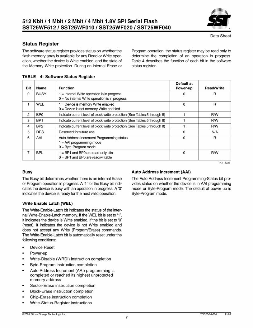
Status RegisterThe software status register provides status on whether theflash memory array is available for any Read or Write oper-ation, whether the device is Write enabled, and the state ofthe Memory Write protection. During an internal Erase or
Program operation, the status register may be read only todetermine the completion of an operation in progress.Table 4 describes the function of each bit in the softwarestatus register.
Busy
The Busy bit determines whether there is an internal Eraseor Program operation in progress. A ‘1’ for the Busy bit indi-cates the device is busy with an operation in progress. A ‘0’indicates the device is ready for the next valid operation.
Write Enable Latch (WEL)
The Write-Enable-Latch bit indicates the status of the inter-nal Write-Enable-Latch memory. If the WEL bit is set to ‘1’,it indicates the device is Write enabled. If the bit is set to ‘0’(reset), it indicates the device is not Write enabled anddoes not accept any Write (Program/Erase) commands.The Write-Enable-Latch bit is automatically reset under thefollowing conditions:
• Device Reset• Power-up• Write-Disable (WRDI) instruction completion• Byte-Program instruction completion• Auto Address Increment (AAI) programming is
completed or reached its highest unprotected memory address
• Sector-Erase instruction completion• Block-Erase instruction completion• Chip-Erase instruction completion• Write-Status-Register instructions
Auto Address Increment (AAI)
The Auto Address Increment Programming-Status bit pro-vides status on whether the device is in AAI programmingmode or Byte-Program mode. The default at power up isByte-Program mode.
TABLE 4: Software Status Register
Bit Name FunctionDefault atPower-up Read/Write
0 BUSY 1 = Internal Write operation is in progress0 = No internal Write operation is in progress
0 R
1 WEL 1 = Device is memory Write enabled0 = Device is not memory Write enabled
0 R
2 BP0 Indicate current level of block write protection (See Tables 5 through 8) 1 R/W
3 BP1 Indicate current level of block write protection (See Tables 5 through 8) 1 R/W
4 BP2 Indicate current level of block write protection (See Tables 5 through 8) 1 R/W
5 RES Reserved for future use 0 N/A
6 AAI Auto Address Increment Programming status1 = AAI programming mode0 = Byte-Program mode
0 R
7 BPL 1 = BP1 and BP0 are read-only bits0 = BP1 and BP0 are read/writable
0 R/W
T4.1 1328
7©2009 Silicon Storage Technology, Inc. S71328-08-000 11/09

Data Sheet
512 Kbit / 1 Mbit / 2 Mbit / 4 Mbit 1.8V SPI Serial FlashSST25WF512 / SST25WF010 / SST25WF020 / SST25WF040
Block-Protection (BP2, BP1, BP0)
The Block-Protection (BP1, BP0) bits define the size of thememory area to be software protected against any mem-ory Write (Program or Erase) operation, see Tables 5-7.The Write-Status-Register (WRSR) instruction is used toprogram the BP1 and BP0 bits as long as WP# is high orthe Block-Protect-Lock (BPL) bit is ‘0’. Chip-Erase can onlybe executed if Block-Protection bits are all ‘0’. After power-up, BP2, BP1, and BP0 are set to defaults. See Table 4 fordefaults at power-up.
Block Protection Lock-Down (BPL)
When the WP# pin is driven low (VIL), it enables the Block-Protection-Lock-Down (BPL) bit. When BPL is set to ‘1’, itprevents any further alteration of the BPL, BP1, and BP0bits. When the WP# pin is driven high (VIH), the BPL bithas no effect and its value is ‘Don’t Care’. After power-up,the BPL bit is reset to ‘0’.
TABLE 5: Software Status Register Block Protection for SST25WF512
Protection Level
Status Register Bit Protected Memory Address
BP11
1. Default at power-up for BP1 and BP0 is ‘11’.
BP0 512 Kbit
None 0 0 None
1 (Upper Quarter Memory) 0 1 00C000H-00FFFFH
2 (Upper Half Memory) 1 0 008000H-00FFFFH
3 (Full Memory) 1 1 000000H-00FFFFHT5.1 1328
TABLE 6: Software Status Register Block Protection for SST25WF010
Protection Level
Status Register Bit Protected Memory Address
BP11
1. Default at power-up for BP1 and BP0 is ‘11’.
BP0 1 Mbit
None 0 0 None
1 (Upper Quarter Memory) 0 1 018000H-01FFFFH
2 (Upper Half Memory) 1 0 010000H-01FFFFH
3 (Full Memory) 1 1 000000H-01FFFFHT6.0 1328
TABLE 7: Software Status Register Block Protection for SST25WF020
Protection Level
Status Register Bit Protected Memory Address
BP11
1. Default at power-up for BP1 and BP0 is ‘11’.
BP0 2 Mbit
None 0 0 None
1 (Upper Quarter Memory) 0 1 030000H-03FFFFH
2 (Upper Half Memory) 1 0 020000H-03FFFFH
3 (Full Memory) 1 1 000000H-03FFFFHT7.0 1328
8©2009 Silicon Storage Technology, Inc. S71328-08-000 11/09

Data Sheet
512 Kbit / 1 Mbit / 2 Mbit / 4 Mbit 1.8V SPI Serial FlashSST25WF512 / SST25WF010 / SST25WF020 / SST25WF040
TABLE 8: Software Status Register Block Protection for SST25WF040
Protection Level Protected Blocks
Status Register Bit Protected Memory Address
BP21 BP1 BP0 4 Mbit
None None 0 0 0 None
1 (Upper Eighth Memory) Blocks 14 through 15 0 0 1 70000H-7FFFFH
2 (Upper Quarter Memory) Blocks 12 through 15 0 1 0 60000H-7FFFFH
3 (Upper Half Memory) Blocks 8 through 15 0 1 1 40000H-7FFFFH
4 (Full Memory) Blocks 0 through 15 1 0 0 00000H-7FFFFH
5 (Full Memory) Blocks 0 through 15 1 0 1 00000H-7FFFFH
6 (Full Memory) Blocks 0 through 15 1 1 0 00000H-7FFFFH
7 (Full Memory) Blocks 0 through 15 1 1 1 00000H-7FFFFHT8.0 1328
1. Default at power-up for BP2, BP1, and BP0 is ‘11’.
9©2009 Silicon Storage Technology, Inc. S71328-08-000 11/09

Data Sheet
512 Kbit / 1 Mbit / 2 Mbit / 4 Mbit 1.8V SPI Serial FlashSST25WF512 / SST25WF010 / SST25WF020 / SST25WF040
INSTRUCTIONS
Instructions are used to read, write (Erase and Program),and configure the SST25WF512/010/020/040. Theinstruction bus cycles are 8 bits each for commands (OpCode), data, and addresses. The Write-Enable (WREN)instruction must be executed prior to Byte-Program, AutoAddress Increment (AAI) programming, Sector-Erase,Block-Erase, Write-Status-Register, or Chip-Erase instruc-tions. The complete instructions are provided in Tables 9and 10. All instructions are synchronized off a high-to-lowtransition of CE#. Inputs will be accepted on the rising edge
of SCK starting with the most significant bit. CE# must bedriven low before an instruction is entered and must bedriven high after the last bit of the instruction has beenshifted in (except for Read, Read-ID, and Read-Status-Register instructions). Any low-to-high transition on CE#,before receiving the last bit of an instruction bus cycle, willterminate the instruction in progress and return the deviceto standby mode. Instruction commands (Op Code),addresses, and data are all input from the most significantbit (MSB) first.
TABLE 9: Device Operation Instructions for SST25WF512 and SST25WF010
Instruction Description Op Code Cycle1
1. One bus cycle is eight clock periods.
Address Cycle(s)2
2. Address bits above the most significant bit of each density can be VIL or VIH.
Dummy Cycle(s)
DataCycle(s)
Maximum Frequency
Read Read Memory 0000 0011b (03H) 3 0 1 to ∞ 20 MHz
High-Speed Read Read Memory at Higher Speed 0000 1011b (0BH) 3 1 1 to ∞
40 MHz
4 KByte Sector-Erase3
3. 4 KByte Sector-Erase addresses: use AMS-A12, remaining addresses are don’t care but must be set either at VIL or VIH.
Erase 4 KByte of memory array
0010 0000b (20H) 3 0 0
32 KByte Block-Erase4
4. 32 KByte Block-Erase addresses: use AMS-A15, remaining addresses are don’t care but must be set either at VIL or VIH.
Erase 32 KByte block of memory array
0101 0010b (52H) 3 0 0
Chip-Erase Erase Full Memory Array 0110 0000b (60H) or 1100 0111b (C7H)
0 0 0
Byte-Program To Program One Data Byte 0000 0010b (02H) 3 0 1
AAI-Word-Program5
5. To continue programming to the next sequential address location, enter the 8-bit command, ADH, followed by 2 bytes of data to be programmed. Data Byte 0 will be programmed into the initial address [A23-A1] with A0=0, Data Byte 1 will be programmed into the initial address [A23-A1] with A0 = 1.
Auto Address Increment Programming
1010 1101b (ADH) 3 0 2 to ∞
RDSR6
6. The Read-Status-Register is continuous with ongoing clock cycles until terminated by a low to high transition on CE#.
Read-Status-Register 0000 0101b (05H) 0 0 1 to ∞
EWSR7
7. Either EWSR or WREN followed by WRSR will write to the Status register. The EWSR-WRSR sequence provides backward compat-ibility to the SST25VF/LF series. The WREN-WRSR sequence is recommended for new designs.
Enable-Write-Status-Register 0110 0000b (50H) 0 0 0
WRSR Write-Status-Register 0000 0001b (01H) 0 0 1
WREN7 Write-Enable 0000 0110b (06H) 0 0 0
WRDI Write-Disable 0000 0100b (04H) 0 0 0
RDID8
8. Manufacturer’s ID is read with A0=0, and Device ID is read with A0=1. All other address bits are 00H. The Manufacturer’s ID and device ID output stream is continuous until terminated by a low-to-high transition on CE#.
Read-ID 1001 0000b (90H) or 1010 1011b (ABH)
3 0 1 to ∞
EBSY Enable SO to output RY/BY# status during AAI programming
0111 0000b (70H) 0 0 0
DBSY Disable SO to output RY/BY# status during AAI programming
1000 0000b (80H) 0 0 0
JEDEC-ID JEDEC ID read 1001 1111b (9FH) 0 0 3 to ∞
EHLD Enable HOLD# pin functionality of the RST#/HOLD# pin
1010 1010b (AAH) 0 0 0
T9.0 1328
10©2009 Silicon Storage Technology, Inc. S71328-08-000 11/09
Data Sheet
512 Kbit / 1 Mbit / 2 Mbit / 4 Mbit 1.8V SPI Serial FlashSST25WF512 / SST25WF010 / SST25WF020 / SST25WF040
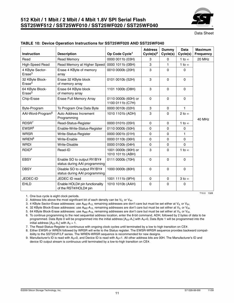
TABLE 10: Device Operation Instructions for SST25WF020 AND SST25WF040
Instruction Description Op Code Cycle1
1. One bus cycle is eight clock periods.
Address Cycle(s)2
2. Address bits above the most significant bit of each density can be VIL or VIH.
Dummy Cycle(s)
DataCycle(s)
Maximum Frequency
Read Read Memory 0000 0011b (03H) 3 0 1 to ∞ 20 MHz
High-Speed Read Read Memory at Higher Speed 0000 1011b (0BH) 3 1 1 to ∞
40 MHz
4 KByte Sector-Erase3
3. 4 KByte Sector-Erase addresses: use AMS-A12, remaining addresses are don’t care but must be set either at VIL or VIH.
Erase 4 KByte of memory array
0010 0000b (20H) 3 0 0
32 KByte Block-Erase4
4. 32 KByte Block-Erase addresses: use AMS-A15, remaining addresses are don’t care but must be set either at VIL or VIH.
Erase 32 KByte block of memory array
0101 0010b (52H) 3 0 0
64 KByte Block-Erase5
5. 64 KByte Block-Erase addresses: use AMS-A16, remaining addresses are don’t care but must be set either at VIL or VIH.
Erase 64 KByte block of memory array
1101 1000b (D8H) 3 0 0
Chip-Erase Erase Full Memory Array 0110 0000b (60H) or 1100 0111b (C7H)
0 0 0
Byte-Program To Program One Data Byte 0000 0010b (02H) 3 0 1
AAI-Word-Program6
6. To continue programming to the next sequential address location, enter the 8-bit command, ADH, followed by 2 bytes of data to be programmed. Data Byte 0 will be programmed into the initial address [A23-A1] with A0=0, Data Byte 1 will be programmed into the initial address [A23-A1] with A0 = 1.
Auto Address Increment Programming
1010 1101b (ADH) 3 0 2 to ∞
RDSR7
7. The Read-Status-Register is continuous with ongoing clock cycles until terminated by a low to high transition on CE#.
Read-Status-Register 0000 0101b (05H) 0 0 1 to ∞
EWSR8
8. Either EWSR or WREN followed by WRSR will write to the Status register. The EWSR-WRSR sequence provides backward compat-ibility to the SST25VF/LF series. The WREN-WRSR sequence is recommended for new designs.
Enable-Write-Status-Register 0110 0000b (50H) 0 0 0
WRSR Write-Status-Register 0000 0001b (01H) 0 0 1
WREN8 Write-Enable 0000 0110b (06H) 0 0 0
WRDI Write-Disable 0000 0100b (04H) 0 0 0
RDID9
9. Manufacturer’s ID is read with A0=0, and Device ID is read with A0=1. All other address bits are 00H. The Manufacturer’s ID and device ID output stream is continuous until terminated by a low-to-high transition on CE#.
Read-ID 1001 0000b (90H) or 1010 1011b (ABH)
3 0 1 to ∞
EBSY Enable SO to output RY/BY# status during AAI programming
0111 0000b (70H) 0 0 0
DBSY Disable SO to output RY/BY# status during AAI programming
1000 0000b (80H) 0 0 0
JEDEC-ID JEDEC ID read 1001 1111b (9FH) 0 0 3 to ∞
EHLD Enable HOLD# pin functionality of the RST#/HOLD# pin
1010 1010b (AAH) 0 0 0
T10.0 1328
11©2009 Silicon Storage Technology, Inc. S71328-08-000 11/09

Data Sheet
512 Kbit / 1 Mbit / 2 Mbit / 4 Mbit 1.8V SPI Serial FlashSST25WF512 / SST25WF010 / SST25WF020 / SST25WF040
Read (20 MHz)The Read instruction, 03H, supports up to 20 MHz Read.The device outputs a data stream starting from the speci-fied address location. The data stream is continuousthrough all addresses until terminated by a low-to-high tran-sition on CE#. The internal address pointer automaticallyincrements until the highest memory address is reached.Once the highest memory address is reached, the addresspointer automatically increments to the beginning (wrap-
around) of the address space. For example, for 2 Mbit den-sity, once the data from the address location 3FFFFH isread, the next output is from address location 000000H.The Read instruction is initiated by executing an 8-bit com-mand, 03H, followed by address bits A23-A0. CE# mustremain active low for the duration of the Read cycle. SeeFigure 6 for the Read sequence.
FIGURE 6: Read Sequence
High-Speed-Read (40 MHz)The High-Speed-Read instruction supporting up to 40 MHzRead is initiated by executing an 8-bit command, 0BH, fol-lowed by address bits [A23-A0] and a dummy byte. CE#must remain active low for the duration of the High-Speed-Read cycle. See Figure 7 for the High-Speed-Readsequence.
Following a dummy cycle, the High-Speed-Read instruc-tion outputs the data starting from the specified addresslocation. The data output stream is continuous through all
addresses until terminated by a low-to-high transition onCE#. The internal address pointer will automatically incre-ment until the highest memory address is reached. Oncethe highest memory address is reached, the addresspointer will automatically increment to the beginning (wrap-around) of the address space. For example, for 2 Mbit den-sity, once the data from address location 3FFFFH is read,the next output will be from address location 000000H.
FIGURE 7: High-Speed-Read Sequence
1328 Fx6.0
CE#
SO
SI
SCK
ADD.
0 1 2 3 4 5 6 7 8
ADD. ADD.03
HIGH IMPEDANCE
15 16 23 24 31 32 39 40 7047 48 55 56 63 64
N+2 N+3 N+4N N+1DOUT
MSB MSB
MSB
MODE 0
MODE 3
DOUT DOUT DOUT DOUT
1328 F07.0
CE#
SO
SI
SCK
ADD.
0 1 2 3 4 5 6 7 8
ADD. ADD.0B
HIGH IMPEDANCE
15 16 23 24 31 32 39 40 47 48 55 56 63 64
N+2 N+3 N+4N N+1
X
MSB
MODE 0
MODE 3
DOUT DOUT DOUT DOUT
8071 72
DOUT
MSB
12©2009 Silicon Storage Technology, Inc. S71328-08-000 11/09
Data Sheet
512 Kbit / 1 Mbit / 2 Mbit / 4 Mbit 1.8V SPI Serial FlashSST25WF512 / SST25WF010 / SST25WF020 / SST25WF040
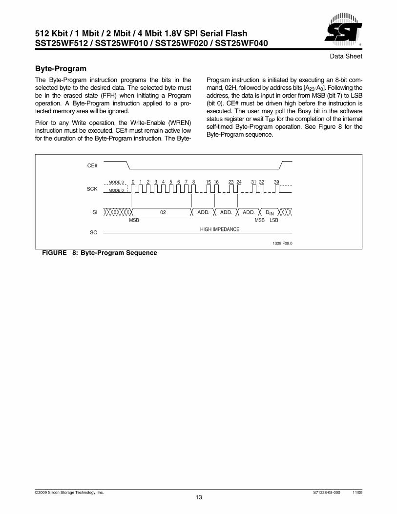
Byte-ProgramThe Byte-Program instruction programs the bits in theselected byte to the desired data. The selected byte mustbe in the erased state (FFH) when initiating a Programoperation. A Byte-Program instruction applied to a pro-tected memory area will be ignored.
Prior to any Write operation, the Write-Enable (WREN)instruction must be executed. CE# must remain active lowfor the duration of the Byte-Program instruction. The Byte-
Program instruction is initiated by executing an 8-bit com-mand, 02H, followed by address bits [A23-A0]. Following theaddress, the data is input in order from MSB (bit 7) to LSB(bit 0). CE# must be driven high before the instruction isexecuted. The user may poll the Busy bit in the softwarestatus register or wait TBP for the completion of the internalself-timed Byte-Program operation. See Figure 8 for theByte-Program sequence.
FIGURE 8: Byte-Program Sequence
1328 F08.0
CE#
SO
SI
SCK
ADD.
0 1 2 3 4 5 6 7 8
ADD. ADD. DIN02
HIGH IMPEDANCE
15 16 23 24 31 32 39
MSB LSB
MODE 3
MODE 0
MSB
13©2009 Silicon Storage Technology, Inc. S71328-08-000 11/09

Data Sheet
512 Kbit / 1 Mbit / 2 Mbit / 4 Mbit 1.8V SPI Serial FlashSST25WF512 / SST25WF010 / SST25WF020 / SST25WF040
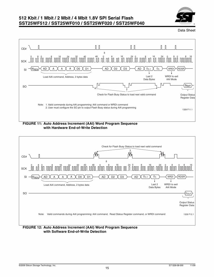
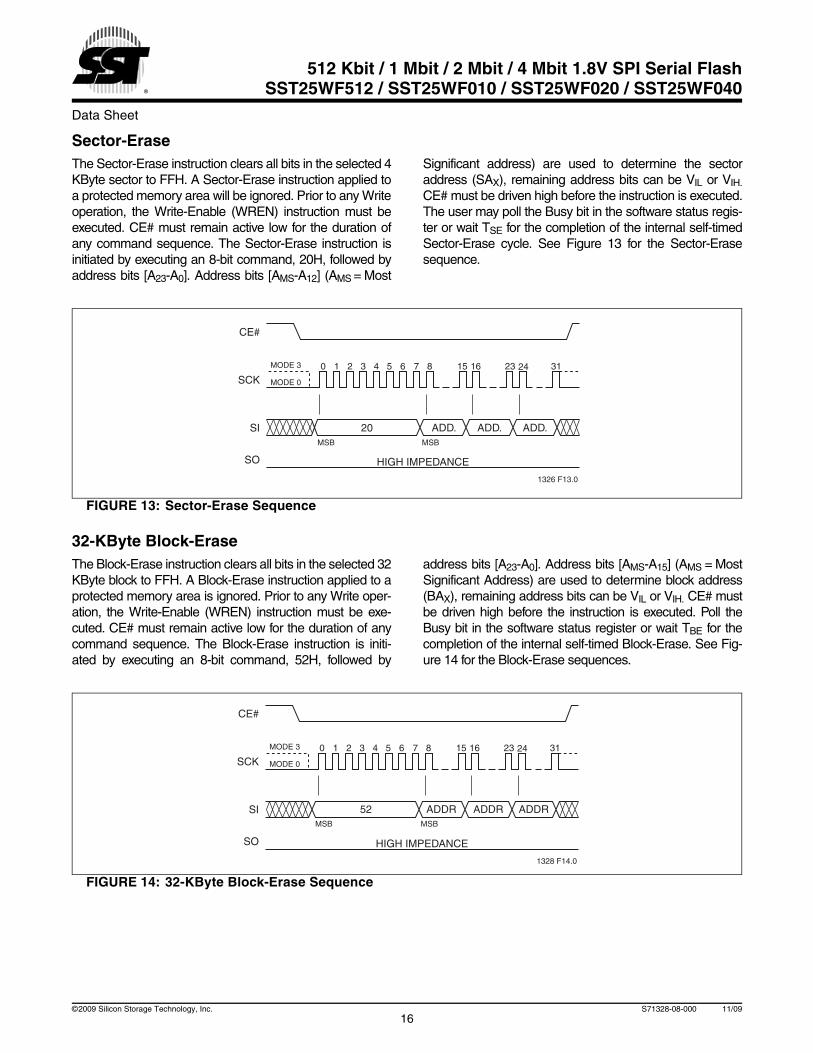
Auto Address Increment (AAI) Word-ProgramThe AAI program instruction allows multiple bytes of data tobe programmed without re-issuing the next sequentialaddress location. This feature decreases total program-ming time when multiple bytes or the entire memory arrayis to be programmed. An AAI Word program instructionpointing to a protected memory area will be ignored. Theselected address range must be in the erased state (FFH)when initiating an AAI Word Program operation. Whilewithin AAI Word Programming sequence, the only validinstructions are AAI Word (ADH), RDSR (05H), or WRDI(04H). Users have three options to determine the comple-tion of each AAI Word program cycle: hardware detectionby reading the Serial Output, software detection by pollingthe BUSY bit in the software status register or wait TBP.Refer to End-Of-Write Detection section for details.
Prior to any write operation, the Write-Enable (WREN)instruction must be executed. The AAI Word Programinstruction is initiated by executing an 8-bit command,ADH, followed by address bits [A23-A0]. Following theaddresses, two bytes of data are input sequentially, eachone from MSB (Bit 7) to LSB (Bit 0). The first byte of data(D0) will be programmed into the initial address [A23-A1]with A0 = 0, the second byte of Data (D1) will be pro-grammed into the initial address [A23-A1] with A0 = 1. CE#must be driven high before the AAI Word Program instruc-tion is executed. The user must check the BUSY statusbefore entering the next valid command. Once the deviceindicates it is no longer busy, data for the next two sequen-tial addresses may be programmed and so on. When thelast desired byte had been entered, check the busy statususing the hardware method or the RDSR instruction andexecute the Write-Disable (WRDI) instruction, 04H, to ter-minate AAI. Check the busy status after WRDI to deter-mine if the device is ready for any command. See Figures11 and 12 for AAI Word programming sequence.
There is no wrap mode during AAI programming; once thehighest unprotected memory address is reached, thedevice will exit AAI operation and reset the Write-Enable-Latch bit (WEL = 0) and the AAI bit (AAI = 0).
End-of-Write Detection
There are three methods to determine completion of a pro-gram cycle during AAI Word programming: hardwaredetection by reading the Serial Output, software detectionby polling the BUSY bit in the Software Status Register orwait TBP.
Hardware End-of-Write Detection
The Hardware End-of-Write detection method eliminatesthe overhead of polling the Busy bit in the Software StatusRegister during an AAI Word program operation. The 8-bitcommand, 70H, configures the Serial Output (SO) pin toindicate Flash Busy status during AAI Word programming,as shown in Figure 9. The 8-bit command, 70H, must beexecuted prior to executing an AAI Word-Program instruc-tion. Once an internal programming operation begins,asserting CE# will immediately drive the status of the inter-nal flash status on the SO pin. A ‘0’ indicates the device isbusy and a ‘1’ indicates the device is ready for the nextinstruction. De-asserting CE# will return the SO pin to tri-state.
The 8-bit command, 80H, disables the Serial Output (SO)pin to output busy status during AAI-Word-program opera-tion, and re-configures SO as an output pin. In this state,the SO pin will function as a normal Serial Output pin. Atthis time, the RDSR command can poll the status of theSoftware Status Register. This is shown in Figure 10.
FIGURE 9: Enable SO as Hardware RY/BY# during AAI Programming
FIGURE 10: Disable SO as Hardware RY/BY# during AAI Programming
CE#
SO
SI
SCK0 1 2 3 4 5 6 7
70
HIGH IMPEDANCE
MODE 0
MODE 3
1328 F09.0
MSB
CE#
SO
SI
SCK0 1 2 3 4 5 6 7
80
HIGH IMPEDANCE
MODE 0
MODE 3
1328 F10.0
MSB
14©2009 Silicon Storage Technology, Inc. S71328-08-000 11/09
Data Sheet
512 Kbit / 1 Mbit / 2 Mbit / 4 Mbit 1.8V SPI Serial FlashSST25WF512 / SST25WF010 / SST25WF020 / SST25WF040
FIGURE 11: Auto Address Increment (AAI) Word Program Sequence with Hardware End-of-Write Detection
FIGURE 12: Auto Address Increment (AAI) Word Program Sequence with Software End-of-Write Detection
0 8 32 244816 24 0400 8
8
8 16 0 8 16 24 0 08 8 16
CE#
SI
SCK
AA AAD D0 AD
SO DOUT
1328 F11.1
D1 D2 D3 AD Dn-1 Dn WRDI RDSR
Last 2Data Bytes
WRDI to exitAAI Mode
Output StatusRegister Data
Check for Flash Busy Status to load next valid command
Load AAI command, Address, 2 bytes data
Note: 1. Valid commands during AAI programming: AAI command or WRDI command 2. User must configure the SO pin to output Flash Busy status during AAI programming
WREN
DOUT
0 8 32 244816 24 0400 8
8
8 16 0 8 16 24 0 08 8 16
CE#
SI
SCK
AA AAD D0 AD
SO DOUT
1328 F12.1
D1 D2 D3 AD Dn-1 Dn WRDI RDSR
Last 2Data Bytes
WRDI to exitAAI Mode
Output StatusRegister Data
Check for Flash Busy Status to load next valid command
Load AAI command, Address, 2 bytes data
Note: Valid commands during AAI programming: AAI command, Read Status Register command, or WRDI command
WREN
15©2009 Silicon Storage Technology, Inc. S71328-08-000 11/09
Data Sheet
512 Kbit / 1 Mbit / 2 Mbit / 4 Mbit 1.8V SPI Serial FlashSST25WF512 / SST25WF010 / SST25WF020 / SST25WF040
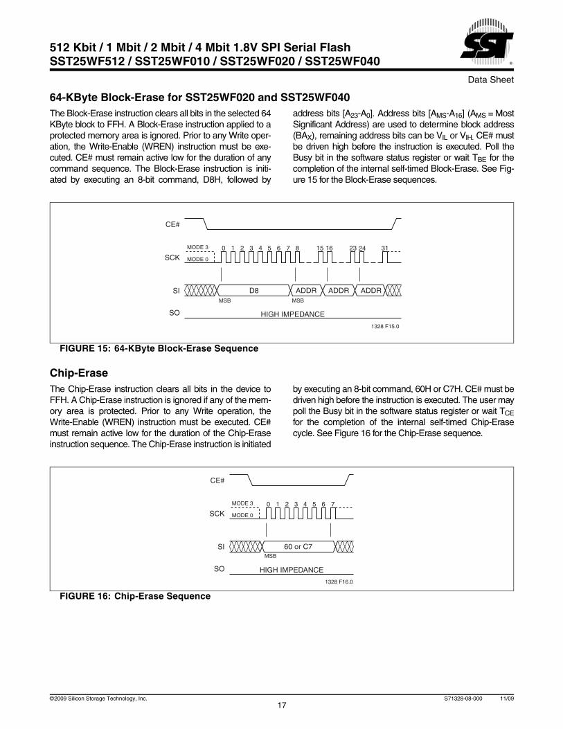
Sector-EraseThe Sector-Erase instruction clears all bits in the selected 4KByte sector to FFH. A Sector-Erase instruction applied toa protected memory area will be ignored. Prior to any Writeoperation, the Write-Enable (WREN) instruction must beexecuted. CE# must remain active low for the duration ofany command sequence. The Sector-Erase instruction isinitiated by executing an 8-bit command, 20H, followed byaddress bits [A23-A0]. Address bits [AMS-A12] (AMS = Most
Significant address) are used to determine the sectoraddress (SAX), remaining address bits can be VIL or VIH.CE# must be driven high before the instruction is executed.The user may poll the Busy bit in the software status regis-ter or wait TSE for the completion of the internal self-timedSector-Erase cycle. See Figure 13 for the Sector-Erasesequence.
FIGURE 13: Sector-Erase Sequence
32-KByte Block-EraseThe Block-Erase instruction clears all bits in the selected 32KByte block to FFH. A Block-Erase instruction applied to aprotected memory area is ignored. Prior to any Write oper-ation, the Write-Enable (WREN) instruction must be exe-cuted. CE# must remain active low for the duration of anycommand sequence. The Block-Erase instruction is initi-ated by executing an 8-bit command, 52H, followed by
address bits [A23-A0]. Address bits [AMS-A15] (AMS = MostSignificant Address) are used to determine block address(BAX), remaining address bits can be VIL or VIH. CE# mustbe driven high before the instruction is executed. Poll theBusy bit in the software status register or wait TBE for thecompletion of the internal self-timed Block-Erase. See Fig-ure 14 for the Block-Erase sequences.
FIGURE 14: 32-KByte Block-Erase Sequence
CE#
SO
SI
SCK
ADD.
0 1 2 3 4 5 6 7 8
ADD. ADD.20
HIGH IMPEDANCE
15 16 23 24 31
MODE 0
MODE 3
1326 F13.0
MSBMSB
CE#
SO
SI
SCK
ADDR
0 1 2 3 4 5 6 7 8
ADDR ADDR52
HIGH IMPEDANCE
15 16 23 24 31
MODE 0
MODE 3
1328 F14.0
MSB MSB
16©2009 Silicon Storage Technology, Inc. S71328-08-000 11/09
Data Sheet
512 Kbit / 1 Mbit / 2 Mbit / 4 Mbit 1.8V SPI Serial FlashSST25WF512 / SST25WF010 / SST25WF020 / SST25WF040
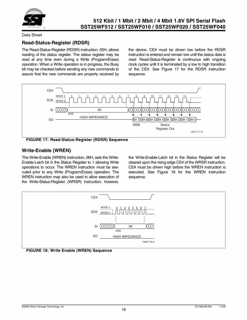
64-KByte Block-Erase for SST25WF020 and SST25WF040The Block-Erase instruction clears all bits in the selected 64KByte block to FFH. A Block-Erase instruction applied to aprotected memory area is ignored. Prior to any Write oper-ation, the Write-Enable (WREN) instruction must be exe-cuted. CE# must remain active low for the duration of anycommand sequence. The Block-Erase instruction is initi-ated by executing an 8-bit command, D8H, followed by
address bits [A23-A0]. Address bits [AMS-A16] (AMS = MostSignificant Address) are used to determine block address(BAX), remaining address bits can be VIL or VIH. CE# mustbe driven high before the instruction is executed. Poll theBusy bit in the software status register or wait TBE for thecompletion of the internal self-timed Block-Erase. See Fig-ure 15 for the Block-Erase sequences.
FIGURE 15: 64-KByte Block-Erase Sequence
Chip-EraseThe Chip-Erase instruction clears all bits in the device toFFH. A Chip-Erase instruction is ignored if any of the mem-ory area is protected. Prior to any Write operation, theWrite-Enable (WREN) instruction must be executed. CE#must remain active low for the duration of the Chip-Eraseinstruction sequence. The Chip-Erase instruction is initiated
by executing an 8-bit command, 60H or C7H. CE# must bedriven high before the instruction is executed. The user maypoll the Busy bit in the software status register or wait TCEfor the completion of the internal self-timed Chip-Erasecycle. See Figure 16 for the Chip-Erase sequence.
FIGURE 16: Chip-Erase Sequence
CE#
SO
SI
SCK
ADDR
0 1 2 3 4 5 6 7 8
ADDR ADDRD8
HIGH IMPEDANCE
15 16 23 24 31
MODE 0
MODE 3
1328 F15.0
MSB MSB
CE#
SO
SI
SCK0 1 2 3 4 5 6 7
60 or C7
HIGH IMPEDANCE
MODE 0
MODE 3
1328 F16.0
MSB
17©2009 Silicon Storage Technology, Inc. S71328-08-000 11/09
Data Sheet
512 Kbit / 1 Mbit / 2 Mbit / 4 Mbit 1.8V SPI Serial FlashSST25WF512 / SST25WF010 / SST25WF020 / SST25WF040
Read-Status-Register (RDSR)The Read-Status-Register (RDSR) instruction, 05H, allowsreading of the status register. The status register may beread at any time even during a Write (Program/Erase)operation. When a Write operation is in progress, the Busybit may be checked before sending any new commands toassure that the new commands are properly received by
the device. CE# must be driven low before the RDSRinstruction is entered and remain low until the status data isread. Read-Status-Register is continuous with ongoingclock cycles until it is terminated by a low to high transitionof the CE#. See Figure 17 for the RDSR instructionsequence.
FIGURE 17: Read-Status-Register (RDSR) Sequence
Write-Enable (WREN)The Write-Enable (WREN) instruction, 06H, sets the Write-Enable-Latch bit in the Status Register to 1 allowing Writeoperations to occur. The WREN instruction must be exe-cuted prior to any Write (Program/Erase) operation. TheWREN instruction may also be used to allow execution ofthe Write-Status-Register (WRSR) instruction; however,
the Write-Enable-Latch bit in the Status Register will becleared upon the rising edge CE# of the WRSR instruction.CE# must be driven high before the WREN instruction isexecuted. See Figure 18 for the WREN instructionsequence.
FIGURE 18: Write Enable (WREN) Sequence
0 1 2 3 4 5 6 7 8 9 10 11 12 13 14
1327 F17.0
MODE 3
SCK
SI
SO
CE#
Bit 7 Bit 6 Bit 5 Bit 4 Bit 3 Bit 2 Bit 1 Bit 0
05
MODE 0
HIGH IMPEDANCE
StatusRegister Out
MSB
MSB
CE#
SO
SI
SCK0 1 2 3 4 5 6 7
06
HIGH IMPEDANCE
MODE 0
MODE 3
1328 F18.0
MSB
18©2009 Silicon Storage Technology, Inc. S71328-08-000 11/09

Data Sheet
512 Kbit / 1 Mbit / 2 Mbit / 4 Mbit 1.8V SPI Serial FlashSST25WF512 / SST25WF010 / SST25WF020 / SST25WF040
Write-Disable (WRDI)The Write-Disable (WRDI) instruction, 04H, resets theWrite-Enable-Latch bit and AAI to 0 disabling any newWrite operations from occurring. The WRDI instruction willnot terminate any programming operation in progress. Any
program operation in progress may continue up to TBP afterexecuting the WRDI instruction. CE# must be driven highbefore the WRDI instruction is executed. See Figure 19 forthe WRDI instruction sequence.
FIGURE 19: Write Disable (WRDI) Sequence
Enable-Write-Status-Register (EWSR)The Enable-Write-Status-Register (EWSR) instructionarms the Write-Status-Register (WRSR) instruction andopens the status register for alteration. The Write-Status-Register instruction must be executed immediately after theexecution of the Enable-Write-Status-Register instruction.This two-step instruction sequence of the EWSR instruc-tion followed by the WRSR instruction works like SDP (soft-ware data protection) command structure which preventsany accidental alteration of the status register values. CE#must be driven low before the EWSR instruction is enteredand must be driven high before the EWSR instruction isexecuted. See Figure 20 for EWSR instruction followed byWRSR instruction.
Write-Status-Register (WRSR)The Write-Status-Register instruction writes new values tothe BP1, BP0, and BPL bits of the status register. CE#must be driven low before the command sequence of the
WRSR instruction is entered and driven high before theWRSR instruction is executed. See Figure 20 for EWSR orWREN and WRSR instruction sequences.
Executing the Write-Status-Register instruction will beignored when WP# is low and BPL bit is set to ‘1’. Whenthe WP# is low, the BPL bit can only be set from ‘0’ to ‘1’ tolock-down the status register, but cannot be reset from ‘1’ to‘0’. When WP# is high, the lock-down function of the BPLbit is disabled and the BPL, BP0, and BP1 bits in the statusregister can all be changed. As long as BPL bit is set to ‘0’or WP# pin is driven high (VIH) prior to the low-to-high tran-sition of the CE# pin at the end of the WRSR instruction,the bits in the status register can all be altered by theWRSR instruction. In this case, a single WRSR instructioncan set the BPL bit to ‘1’ to lock down the status register aswell as altering the BP0, and BP1 bits at the same time.See Table 3 for a summary description of WP# and BPLfunctions.
FIGURE 20: Enable-Write-Status-Register (EWSR) or Write-Enable (WREN) and Write-Status-Register (WRSR) Sequence
CE#
SO
SI
SCK0 1 2 3 4 5 6 7
04
HIGH IMPEDANCE
MODE 0
MODE 3
1328 Fx19.0
MSB
1328 F20.0
MODE 3
HIGH IMPEDANCE
MODE 0
STATUSREGISTER IN
7 6 5 4 3 2 1 0
MSBMSBMSB
01
MODE 3
SCK
SI
SO
CE#
MODE 0
50 or 06
0 1 2 3 4 5 6 7 0 1 2 3 4 5 6 7 8 9 10 11 12 13 14 15
19©2009 Silicon Storage Technology, Inc. S71328-08-000 11/09
Data Sheet
512 Kbit / 1 Mbit / 2 Mbit / 4 Mbit 1.8V SPI Serial FlashSST25WF512 / SST25WF010 / SST25WF020 / SST25WF040
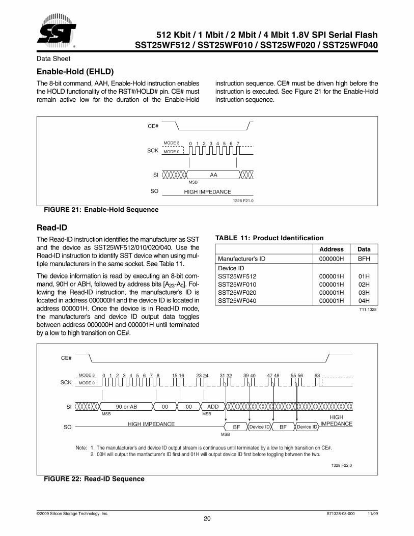
Enable-Hold (EHLD)The 8-bit command, AAH, Enable-Hold instruction enablesthe HOLD functionality of the RST#/HOLD# pin. CE# mustremain active low for the duration of the Enable-Hold
instruction sequence. CE# must be driven high before theinstruction is executed. See Figure 21 for the Enable-Holdinstruction sequence.
FIGURE 21: Enable-Hold Sequence
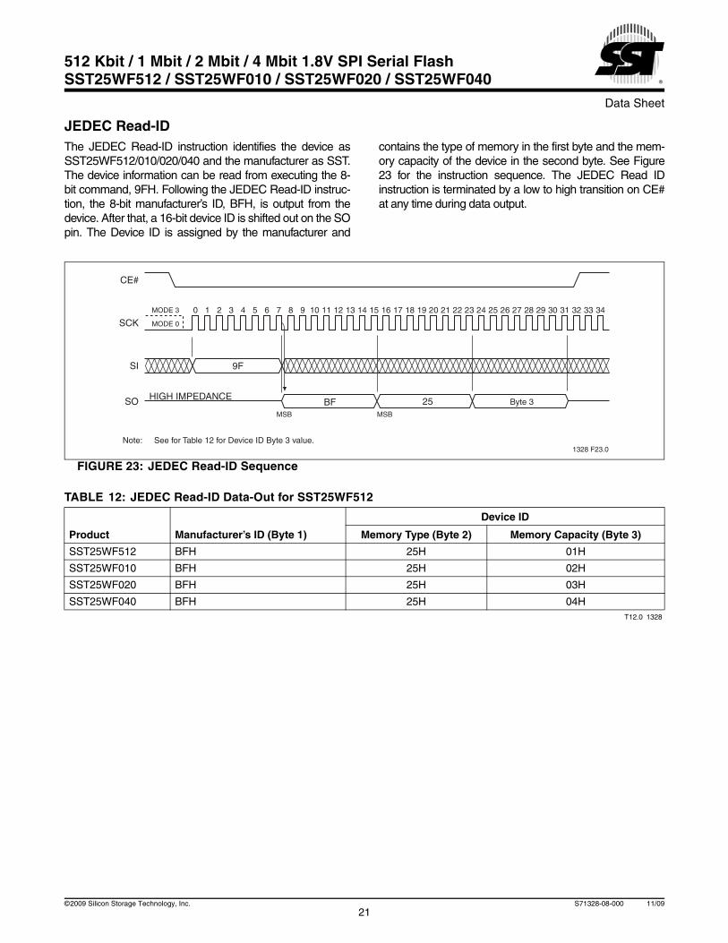
Read-IDThe Read-ID instruction identifies the manufacturer as SSTand the device as SST25WF512/010/020/040. Use theRead-ID instruction to identify SST device when using mul-tiple manufacturers in the same socket. See Table 11.
The device information is read by executing an 8-bit com-mand, 90H or ABH, followed by address bits [A23-A0]. Fol-lowing the Read-ID instruction, the manufacturer’s ID islocated in address 000000H and the device ID is located inaddress 000001H. Once the device is in Read-ID mode,the manufacturer’s and device ID output data togglesbetween address 000000H and 000001H until terminatedby a low to high transition on CE#.
FIGURE 22: Read-ID Sequence
CE#
SO
SI
SCK0 1 2 3 4 5 6 7
AA
HIGH IMPEDANCE
MODE 0
MODE 3
1328 F21.0
MSB
TABLE 11: Product Identification
Address Data
Manufacturer’s ID 000000H BFH
Device ID SST25WF512SST25WF010SST25WF020SST25WF040
000001H000001H000001H000001H
01H02H03H04HT11.1328
1328 F22.0
CE#
SO
SI
SCK
00
0 1 2 3 4 5 6 7 8
00 ADD90 or AB
HIGH IMPEDANCE
15 16 23 24 31 32 39 40 47 48 55 56 63
BF Device ID BF Device ID
Note: 1. The manufacturer's and device ID output stream is continuous until terminated by a low to high transition on CE#. 2. 00H will output the manfacturer's ID first and 01H will output device ID first before toggling between the two.
HIGHIMPEDANCE
MODE 3
MODE 0
MSB MSB
MSB
20©2009 Silicon Storage Technology, Inc. S71328-08-000 11/09
Data Sheet
512 Kbit / 1 Mbit / 2 Mbit / 4 Mbit 1.8V SPI Serial FlashSST25WF512 / SST25WF010 / SST25WF020 / SST25WF040
JEDEC Read-IDThe JEDEC Read-ID instruction identifies the device asSST25WF512/010/020/040 and the manufacturer as SST.The device information can be read from executing the 8-bit command, 9FH. Following the JEDEC Read-ID instruc-tion, the 8-bit manufacturer’s ID, BFH, is output from thedevice. After that, a 16-bit device ID is shifted out on the SOpin. The Device ID is assigned by the manufacturer and
contains the type of memory in the first byte and the mem-ory capacity of the device in the second byte. See Figure23 for the instruction sequence. The JEDEC Read IDinstruction is terminated by a low to high transition on CE#at any time during data output.
FIGURE 23: JEDEC Read-ID Sequence
TABLE 12: JEDEC Read-ID Data-Out for SST25WF512
Device ID
Product Manufacturer’s ID (Byte 1) Memory Type (Byte 2) Memory Capacity (Byte 3)
SST25WF512 BFH 25H 01H
SST25WF010 BFH 25H 02H
SST25WF020 BFH 25H 03H
SST25WF040 BFH 25H 04HT12.0 1328
25 Byte 3
Note: See for Table 12 for Device ID Byte 3 value.1328 F23.0
CE#
SO
SI
SCK0 1 2 3 4 5 6 7 8
HIGH IMPEDANCE
15 1614 28 29 30 31
BF
MODE 3
MODE 0
MSBMSB
9 10 11 12 13 17 18 32 34
9F
19 20 21 22 23 3324 25 26 27
21©2009 Silicon Storage Technology, Inc. S71328-08-000 11/09
Data Sheet
512 Kbit / 1 Mbit / 2 Mbit / 4 Mbit 1.8V SPI Serial FlashSST25WF512 / SST25WF010 / SST25WF020 / SST25WF040
ELECTRICAL SPECIFICATIONS
Absolute Maximum Stress Ratings (Applied conditions greater than those listed under “Absolute MaximumStress Ratings” may cause permanent damage to the device. This is a stress rating only and functional operationof the device at these conditions or conditions greater than those defined in the operational sections of this datasheet is not implied. Exposure to absolute maximum stress rating conditions may affect device reliability.)
Temperature Under Bias . . . . . . . . . . . . . . . . . . . . . . . . . . . . . . . . . . . . . . . . . . . . . . . . . . . . . . . . . -55°C to +125°CStorage Temperature . . . . . . . . . . . . . . . . . . . . . . . . . . . . . . . . . . . . . . . . . . . . . . . . . . . . . . . . . . . . -65°C to +150°CD. C. Voltage on Any Pin to Ground Potential . . . . . . . . . . . . . . . . . . . . . . . . . . . . . . . . . . . . . . . . -0.5V to VDD+0.5VTransient Voltage (<20 ns) on Any Pin to Ground Potential . . . . . . . . . . . . . . . . . . . . . . . . . . . . . . -2.0V to VDD+2.0VPackage Power Dissipation Capability (TA = 25°C) . . . . . . . . . . . . . . . . . . . . . . . . . . . . . . . . . . . . . . . . . . . . . . 1.0WSurface Mount Solder Reflow Temperature . . . . . . . . . . . . . . . . . . . . . . . . . . . . . . . . . . . . . . . 260°C for 10 secondsOutput Short Circuit Current1. . . . . . . . . . . . . . . . . . . . . . . . . . . . . . . . . . . . . . . . . . . . . . . . . . . . . . . . . . . . . . 50 mA
1. Output shorted for no more than one second. No more than one output shorted at a time.
Operating Range
Range Ambient Temp VDD
Industrial -40°C to +85°C 1.65-1.95V
Industrial (extended)1
1. Contact SST Sales for available extended industrial temperature devices.
-40°C to +105°C 1.70-1.90V
AC Conditions of Test
Input Rise/Fall Time . . . . . . . . . . . . . . 5 ns
Output Load . . . . . . . . . . . . . . . . . . . . CL = 30 pF
22©2009 Silicon Storage Technology, Inc. S71328-08-000 11/09

Data Sheet
512 Kbit / 1 Mbit / 2 Mbit / 4 Mbit 1.8V SPI Serial FlashSST25WF512 / SST25WF010 / SST25WF020 / SST25WF040
Power-Up SpecificationsAll functionalities and DC specifications are specified for a VDD ramp rate of greater than 1V per 100 ms (0V to 1.8Vin less than 180 ms). If the VDD ramp rate is slower than 1V/100 µs, a hardware reset is required. The recom-mended VDD power-up to RESET# high time should be greater than 100 µs to ensure a proper reset. See Table 13and Figures 24 and 25 for more information.
FIGURE 24: Power-Up Reset Diagram
TABLE 13: Recommended System Power-up Timings
Symbol Parameter Minimum Units
TPU-READ1
1. This parameter is measured only for initial qualification and after a design or process change that could affect this parameter.
VDD Min to Read Operation 100 µs
TPU-WRITE1 VDD Min to Write Operation 100 µs
T13.0 1328
1328 F37.1
VDD
RESET#
CE#
TPU-READ
VDD min
0V
VIH
TRECR
Note: See Table 2 on page 5 for TRECR parameter.
23©2009 Silicon Storage Technology, Inc. S71328-08-000 11/09

Data Sheet
512 Kbit / 1 Mbit / 2 Mbit / 4 Mbit 1.8V SPI Serial FlashSST25WF512 / SST25WF010 / SST25WF020 / SST25WF040
FIGURE 25: Power-up Timing Diagram
Time
VDD Min
VDD Max
VDD
Device fully accessibleTPU-READTPU-WRITE
Chip selection is not allowed.Commands may not be accepted or properly
interpreted by the device.
1326 F27.0
24©2009 Silicon Storage Technology, Inc. S71328-08-000 11/09

Data Sheet
512 Kbit / 1 Mbit / 2 Mbit / 4 Mbit 1.8V SPI Serial FlashSST25WF512 / SST25WF010 / SST25WF020 / SST25WF040
DC Characteristics
TABLE 14: DC Operating Characteristics
Symbol Parameter
Limits
Test ConditionsMin Typ1
1. Value characterized, not fully tested in production.
Max Units
IDDR Read Current 2 5 mA CE#=0.1 VDD/0.9 VDD@20 MHz, SO=open
IDDR2 Read Current 4 10 mA CE#=0.1 VDD/0.9VDD@40 MHz, SO=open
IDDW Program and Erase Current 6 10 mA CE#=VDD
ISB Standby Current 2 8 µA CE#=VDD, VIN=VDD or VSS
ILI Input Leakage Current 1 µA VIN=GND to VDD, VDD=VDD Max
ILO Output Leakage Current 1 µA VOUT=GND to VDD, VDD=VDD Max
VIL Input Low Voltage 0.3 V VDD=VDD Min
VIH Input High Voltage 0.7 VDD V VDD=VDD Max
VOL Output Low Voltage 0.2 V IOL=100 µA, VDD=VDD Min
VOH Output High Voltage VDD-0.2 V IOH=-100 µA, VDD=VDD MinT14.0 1328
TABLE 15: Capacitance (TA = 25°C, f=1 Mhz, other pins open)
Parameter Description Test Condition Maximum
COUT1
1. This parameter is measured only for initial qualification and after a design or process change that could affect this parameter.
Output Pin Capacitance VOUT = 0V 12 pF
CIN1 Input Capacitance VIN = 0V 6 pF
T15.0 1328
TABLE 16: Reliability Characteristics
Symbol Parameter Minimum Specification Units Test Method
NEND1
1. This parameter is measured only for initial qualification and after a design or process change that could affect this parameter.
Endurance 100,000 Cycles JEDEC Standard A117
TDR1 Data Retention 100 Years JEDEC Standard A103
ILTH1 Latch Up 100 + IDD mA JEDEC Standard 78
T16.0 1328
25©2009 Silicon Storage Technology, Inc. S71328-08-000 11/09

Data Sheet
512 Kbit / 1 Mbit / 2 Mbit / 4 Mbit 1.8V SPI Serial FlashSST25WF512 / SST25WF010 / SST25WF020 / SST25WF040
AC Characteristics
TABLE 17: AC Operating Characteristics
Limits - 20 MHz Limits - 40 MHz
Symbol Parameter Min Max Min Max Units
FCLK1
1. Maximum clock frequency for Read instruction, 03H, is 20 MHz
Serial Clock Frequency 20 40 MHz
TSCKH Serial Clock High Time 20 11 ns
TSCKL Serial Clock Low Time 20 11 ns
TSCKR Serial Clock Rise Time 5 5 ns
TSCKF Serial Clock Fall Time 5 5 ns
TCES2
2. Relative to SCK
CE# Active Setup Time 20 8 ns
TCEH2 CE# Active Hold Time 20 8 ns
TCHS2 CE# Not Active Setup Time 10 10 ns
TCHH2 CE# Not Active Hold Time 10 10 ns
TCPH CE# High Time 50 25 ns
TCHZ CE# High to High-Z Output 20 19 ns
TCLZ SCK Low to Low-Z Output 0 0 ns
TDS Data In Setup Time 5 2 ns
TDH Data In Hold Time 5 5 ns
THLS HOLD# Low Setup Time 10 8 ns
THHS HOLD# High Setup Time 10 8 ns
THLH HOLD# Low Hold Time 15 12 ns
THHH HOLD# High Hold Time 10 10 ns
THZ HOLD# Low to High-Z Output 20 20 ns
TLZ HOLD# High to Low-Z Output 20 20 ns
TOH Output Hold from SCK Change 0 0 ns
TV Output Valid from SCK 20 9 ns
TSE Sector-Erase 75 75 ms
TBE Block-Erase 75 75 ms
TSCE Chip-Erase 150 150 ms
TBP3
3. AAI-Word Program TBP maximum specification is also at 60 µs maximum time
Byte-Program 60 60 µsT17.1 1328
26©2009 Silicon Storage Technology, Inc. S71328-08-000 11/09

Data Sheet
512 Kbit / 1 Mbit / 2 Mbit / 4 Mbit 1.8V SPI Serial FlashSST25WF512 / SST25WF010 / SST25WF020 / SST25WF040
FIGURE 26: Serial Input Timing Diagram
FIGURE 27: Serial Output Timing Diagram
HIGH-Z HIGH-Z
CE#
SO
SI
SCK
MSB LSB
TDS TDH
TCHHTCES
TCEHTCHS
TSCKRTSCKF
TCPH
1326 F24.0
1328 F25.0
CE#
SI
SO
SCK
MSB
TCLZ
TV
TSCKH
TCHZTOH
TSCKL
LSB
27©2009 Silicon Storage Technology, Inc. S71328-08-000 11/09

Data Sheet
512 Kbit / 1 Mbit / 2 Mbit / 4 Mbit 1.8V SPI Serial FlashSST25WF512 / SST25WF010 / SST25WF020 / SST25WF040
FIGURE 28: Hold Timing Diagram
FIGURE 29: AC Input/Output Reference Waveforms
THZ TLZ
THHH THLS
THLH
THHS
1328 F26.0
HOLD#
CE#
SCK
SO
SI
1326 F28.0
REFERENCE POINTS OUTPUTINPUT
VHT
VLT
VHT
VLT
VIHT
VILT
AC test inputs are driven at VIHT (0.9VDD) for a logic ‘1’ and VILT (0.1VDD) for a logic ‘0’. Measurement reference points forinputs and outputs are VHT (0.6VDD) and VLT (0.4VDD). Input rise and fall times (10% ↔ 90%) are <5 ns.
Note: VHT - VHIGH TestVLT - VLOW TestVIHT - VINPUT HIGH TestVILT - VINPUT LOW Test
28©2009 Silicon Storage Technology, Inc. S71328-08-000 11/09

Data Sheet
512 Kbit / 1 Mbit / 2 Mbit / 4 Mbit 1.8V SPI Serial FlashSST25WF512 / SST25WF010 / SST25WF020 / SST25WF040
PRODUCT ORDERING INFORMATION
Valid combinations for SST25WF512
SST25WF512-40-5I-SAF
Valid combinations for SST25WF010
SST25WF010-40-5I-SAF
Valid combinations for SST25WF020
SST25WF020-40-5I-SAF SST25WF020-40-5I-QAE
Valid combinations for SST25WF040
SST25WF040-40-5I-SAF SST25WF040-40-5I-QAE
Note: Valid combinations are those products in mass production or will be in mass production. Consult your SST sales representative to confirm availability of valid combinations and to determine availability of new combinations.
SST 25 WF XXX - 40 - 5I - SA FXX XX XXX - XX - XX - XX X
Environmental AttributeE1 = non-PbF2 = non-Pb / non-Sn contact (lead) finish:Nickel plating with Gold top (outer) layer
Package ModifierA = 8 leads
Package TypeQ= WSONS = SOIC 150 mil body width
Temperature RangeI = Industrial = -40°C to +85°C
Minimum Endurance5 = 100,000 cycles
Operating Frequency40 = 40 MHz
Device Density512 = 512 Kbit010 = 1 Mbit020 = 2 Mbit040 = 4 Mbit
VoltageW= 1.65-1.95V
Product Series25 = Serial Peripheral Interface flash memory
1. Environmental suffix “E” denotes non-Pb solder. SST non-Pb solder devices are “RoHS Compliant”.
2. Environmental suffix “F” denotes non-Pb/non-SN solder. SST non-Pb/non-Sn solder devices are “RoHS Compliant”.
29©2009 Silicon Storage Technology, Inc. S71328-08-000 11/09
Data Sheet
512 Kbit / 1 Mbit / 2 Mbit / 4 Mbit 1.8V SPI Serial FlashSST25WF512 / SST25WF010 / SST25WF020 / SST25WF040
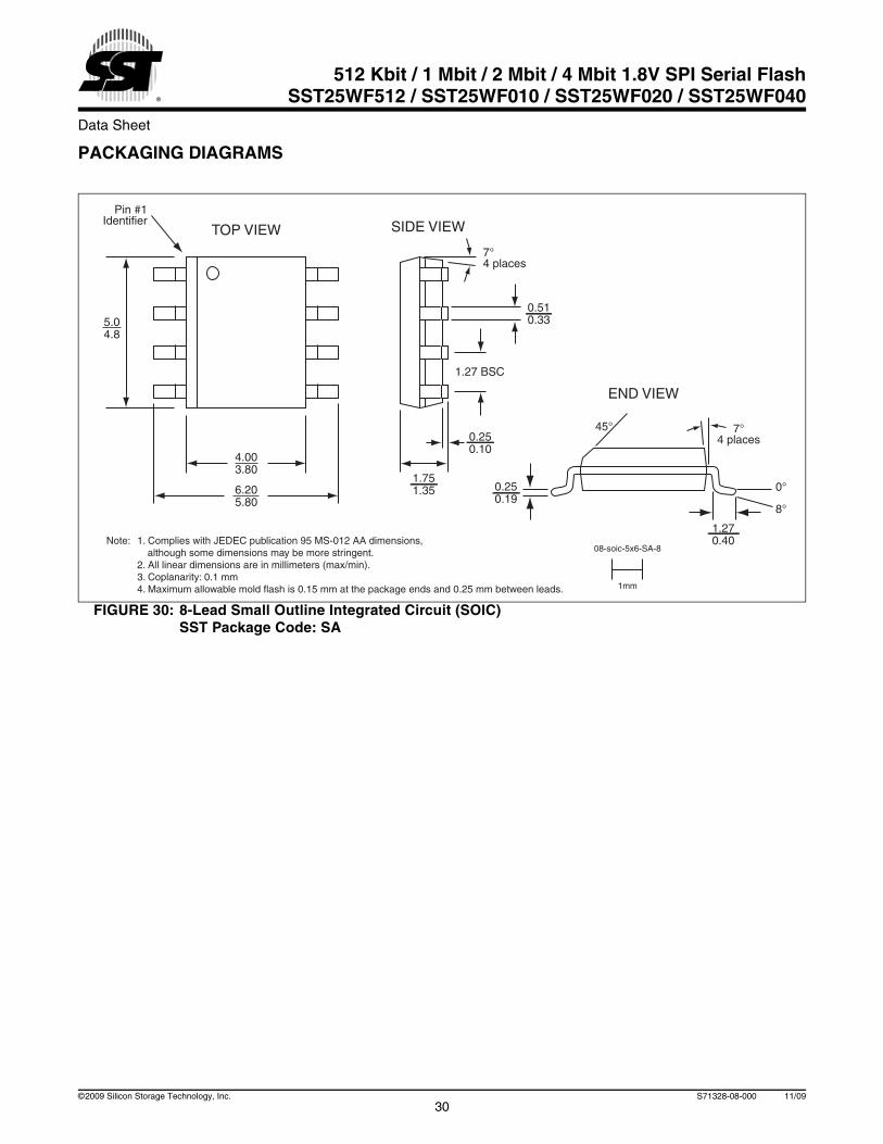
PACKAGING DIAGRAMS
FIGURE 30: 8-Lead Small Outline Integrated Circuit (SOIC)SST Package Code: SA
08-soic-5x6-SA-8Note: 1. Complies with JEDEC publication 95 MS-012 AA dimensions, although some dimensions may be more stringent. 2. All linear dimensions are in millimeters (max/min). 3. Coplanarity: 0.1 mm 4. Maximum allowable mold flash is 0.15 mm at the package ends and 0.25 mm between leads.
TOP VIEW SIDE VIEW
END VIEW
5.04.8
6.205.80
4.003.80
Pin #1Identifier
0.510.33
1.27 BSC
0.250.10
1.751.35
7°4 places
0.250.19
1.270.40
45° 7°4 places
0°
8°
1mm
30©2009 Silicon Storage Technology, Inc. S71328-08-000 11/09
Data Sheet
512 Kbit / 1 Mbit / 2 Mbit / 4 Mbit 1.8V SPI Serial FlashSST25WF512 / SST25WF010 / SST25WF020 / SST25WF040
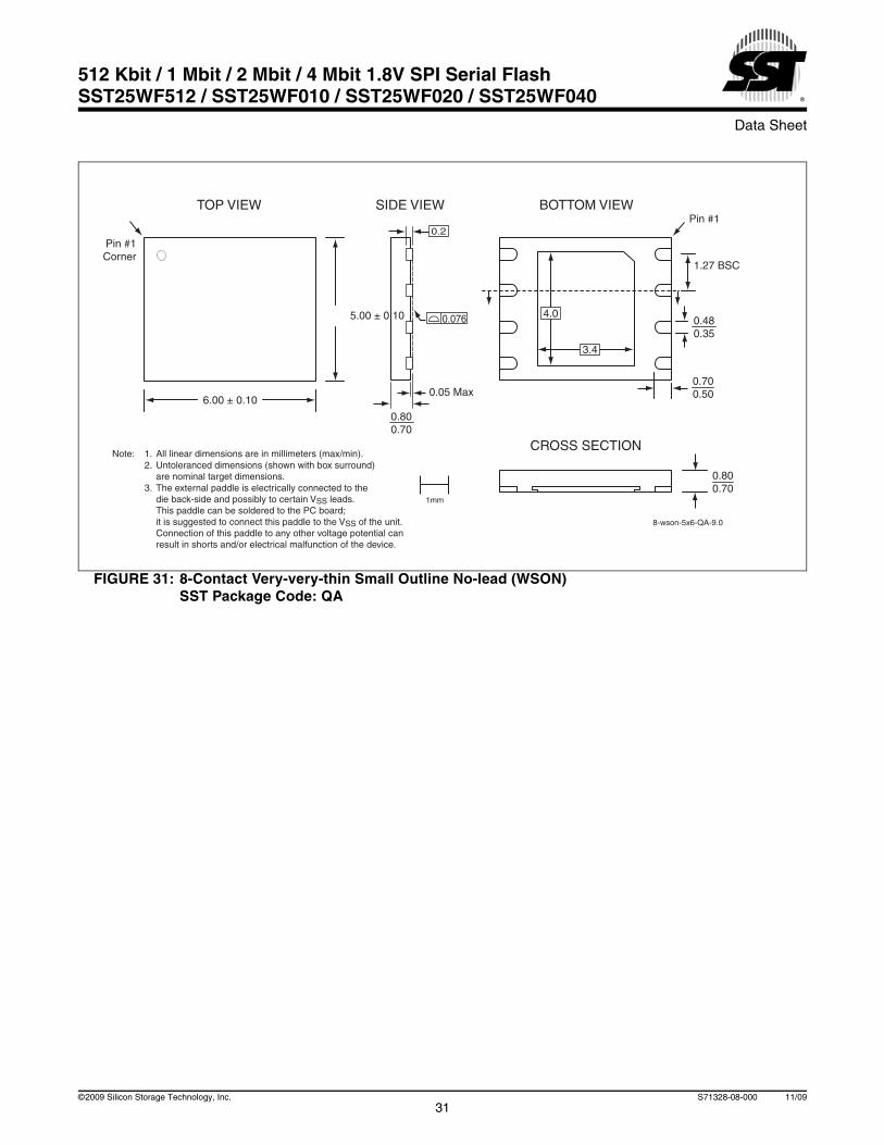
FIGURE 31: 8-Contact Very-very-thin Small Outline No-lead (WSON)SST Package Code: QA
Note: 1. All linear dimensions are in millimeters (max/min). 2. Untoleranced dimensions (shown with box surround) are nominal target dimensions. 3. The external paddle is electrically connected to the die back-side and possibly to certain VSS leads. This paddle can be soldered to the PC board; it is suggested to connect this paddle to the VSS of the unit. Connection of this paddle to any other voltage potential can result in shorts and/or electrical malfunction of the device.
8-wson-5x6-QA-9.0
4.0
1.27 BSC
Pin #1
0.480.35
0.076
3.4
5.00 ± 0.10
6.00 ± 0.100.05 Max
0.700.50
0.800.70
0.800.70
Pin #1Corner
TOP VIEW BOTTOM VIEW
CROSS SECTION
SIDE VIEW
1mm
0.2
31©2009 Silicon Storage Technology, Inc. S71328-08-000 11/09
Data Sheet
512 Kbit / 1 Mbit / 2 Mbit / 4 Mbit 1.8V SPI Serial FlashSST25WF512 / SST25WF010 / SST25WF020 / SST25WF040
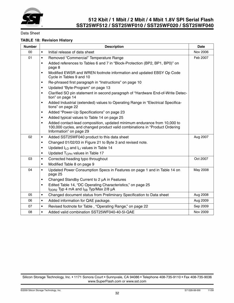
TABLE 18: Revision History
Number Description Date
00 • Initial release of data sheet Nov 2006
01 • Removed “Commercial” Temperature Range• Added references to Tables 6 and 7 in “Block-Protection (BP2, BP1, BP0)” on
page 8• Modified EWSR and WREN footnote information and updated EBSY Op Code
Cycle in Tables 9 and 10• Re-phrased first paragraph in “Instructions” on page 10• Updated “Byte-Program” on page 13• Clarified SO pin statement in second paragraph of “Hardware End-of-Write Detec-
tion” on page 14• Added Industrial (extended) values to Operating Range in “Electrical Specifica-
tions” on page 22• Added “Power-Up Specifications” on page 23• Added typical values to Table 14 on page 25• Added contact-lead composition, updated minimum endurance from 10,000 to
100,000 cycles, and changed product valid combinations in “Product Ordering Information” on page 29
Feb 2007
02 • Added SST25WF040 product to this data sheet• Changed 01/02/03 in Figure 21 to Byte 3 and revised note.• Updated ILO and ILI values in Table 14• Updated TCPH values in Table 17
Aug 2007
03 • Corrected heading typo throughout• Modified Table 8 on page 9
Oct 2007
04 • Updated Power Consumption Specs in Features on page 1 and in Table 14 on page 25
• Changed Standby Current to 2 µA in Features• Edited Table 14, “DC Operating Characteristics,” on page 25
IDDR2 Typ 4 mA and ISB Typ/Max 2/8 µA
May 2008
05 • Changed document status from Preliminary Specification to Data sheet Aug 2008
06 • Added information for QAE package. Aug 2009
07 • Revised footnote for Table , “Operating Range,” on page 22 Sep 2009
08 • Added valid combination SST25WF040-40-5I-QAE Nov 2009
Silicon Storage Technology, Inc. • 1171 Sonora Court • Sunnyvale, CA 94086 • Telephone 408-735-9110 • Fax 408-735-9036www.SuperFlash.com or www.sst.com
32©2009 Silicon Storage Technology, Inc. S71328-08-000 11/09