2 mbit / 3 mbit / 4 mbit / 8 mbit firmware hub - · pdf file– firmware hub interface...
TRANSCRIPT
©2003 Silicon Storage Technology, Inc.S71161-07-000 6/031
The SST logo and SuperFlash are registered trademarks of Silicon Storage Technology, Inc.Intel is a registered trademark of Intel Corporation.
These specifications are subject to change without notice.
Advance InformationFEATURES:
• Firmware Hub for Intel 8xx Chipsets• 2 Mbit, 3 Mbit, 4 Mbit, or 8 Mbit SuperFlash
memory array for code/data storage– SST49LF002A: 256K x8 (2 Mbit)– SST49LF003A: 384K x8 (3 Mbit)– SST49LF004A: 512K x8 (4 Mbit)– SST49LF008A: 1024K x8 (8 Mbit)
• Flexible Erase Capability– Uniform 4 KByte Sectors – Uniform 16 KByte overlay blocks for
SST49LF002A – Uniform 64 KByte overlay blocks for
SST49LF003A/004A/008A – Top Boot Block protection
- 16 KByte for SST49LF002A - 64 KByte for SST49LF003A/004A/008A
– Chip-Erase for PP Mode Only• Single 3.0-3.6V Read and Write Operations• Superior Reliability
– Endurance:100,000 Cycles (typical)– Greater than 100 years Data Retention
• Low Power Consumption– Active Read Current: 6 mA (typical)– Standby Current: 10 µA (typical)
• Fast Sector-Erase/Byte-Program Operation– Sector-Erase Time: 18 ms (typical)– Block-Erase Time: 18 ms (typical)– Chip-Erase Time: 70 ms (typical)– Byte-Program Time: 14 µs (typical)– Chip Rewrite Time:
SST49LF002A: 4 seconds (typical)SST49LF003A: 6 seconds (typical)SST49LF004A: 8 seconds (typical)SST49LF008A: 15 seconds (typical)
– Single-pulse Program or Erase– Internal timing generation
• Two Operational Modes– Firmware Hub Interface (FWH) Mode for
In-System operation– Parallel Programming (PP) Mode for fast
production programming• Firmware Hub Hardware Interface Mode
– 5-signal communication interface supporting byte Read and Write
– 33 MHz clock frequency operation– WP# and TBL# pins provide hardware write
protect for entire chip and/or top Boot Block– Block Locking Register for all blocks– Standard SDP Command Set– Data# Polling and Toggle Bit for End-of-Write
detection– 5 GPI pins for system design flexibility– 4 ID pins for multi-chip selection
• Parallel Programming (PP) Mode– 11-pin multiplexed address and
8-pin data I/O interface– Supports fast In-System or PROM programming
for manufacturing• CMOS and PCI I/O Compatibility• Packages Available
– 32-lead PLCC– 32-lead TSOP (8mm x 14mm)– 40-lead TSOP (10mm x 20mm) SST49LF008A only
PRODUCT DESCRIPTION
The SST49LF00xA flash memory devices are designed tobe read-compatible with the Intel 82802 Firmware Hub(FWH) device for PC-BIOS application. These devices pro-vide protection for the storage and update of code and datain addition to adding system design flexibility through fivegeneral purpose inputs. Two interface modes are sup-ported by the SST49LF00xA: Firmware Hub (FWH) Inter-face mode for in-system programming and ParallelProgramming (PP) mode for fast factory programming ofPC-BIOS applications.
The SST49LF00xA flash memory devices are manufac-tured with SST’s proprietary, high performance SuperFlashtechnology. The split-gate cell design and thick-oxide tun-neling injector attain better reliability and manufacturabilitycompared with alternate approaches. The SST49LF00xAdevices significantly improve performance and reliability,while lowering power consumption. The SST49LF00xAdevices write (Program or Erase) with a single 3.0-3.6Vpower supply. It uses less energy during Erase and Pro-gram than alternative flash memory technologies. The totalenergy consumed is a function of the applied voltage, cur-rent and time of application. Since for any given voltage
2 Mbit / 3 Mbit / 4 Mbit / 8 Mbit Firmware HubSST49LF002A / SST49LF003A / SST49LF004A / SST49LF008A
SST49LF002A / 003A / 004A / 008A2 Mb / 3 Mb / 4 Mb / 8 Mb Firmware Hub for Intel 8xx Chipsets
2
Advance Information
2 Mbit / 3 Mbit / 4 Mbit / 8 Mbit Firmware HubSST49LF002A / SST49LF003A / SST49LF004A / SST49LF008A
©2003 Silicon Storage Technology, Inc. S71161-07-000 6/03
range, the SuperFlash technology uses less current to pro-gram and has a shorter Erase time, the total energy con-sumed during any Erase or Program operation is less thanalternative flash memory technologies. The SST49LF00xAproducts provide a maximum Byte-Program time of 20µsec. The entire memory can be erased and programmedbyte-by-byte typically in 15 seconds for an 8-Mbit device,when using status detection features such as Toggle Bit orData# Polling to indicate the completion of Program opera-tion. The SuperFlash technology provides fixed Erase andProgram time, independent of the number of Erase/Pro-gram cycles that have performed. Therefore the systemsoftware or hardware does not have to be calibrated or cor-related to the cumulated number of Erase/Program cyclesas is necessary with alternative flash memory technolo-gies, whose Erase and Program time increase with accu-mulated Erase/Program cycles.
To protect against inadvertent write, the SST49LF00xAdevices employ hardware and software data (SDP) protec-tion schemes. It is offered with typical endurance of100,000 cycles. Data retention is rated at greater than 100years.
To meet high density, surface mount requirements, theSST49LF00xA device is offered in 32-lead TSOP and 32-lead PLCC packages. In addition, the SST49LF008A isoffered in a 40-lead TSOP package. See Figures 1, 2, and3 for pin assignments and Table 1 for pin descriptions.
Advance Information
2 Mbit / 3 Mbit / 4 Mbit / 8 Mbit Firmware HubSST49LF002A / SST49LF003A / SST49LF004A / SST49LF008A
3©2003 Silicon Storage Technology, Inc. S71161-07-000 6/03
TABLE OF CONTENTS
PRODUCT DESCRIPTION . . . . . . . . . . . . . . . . . . . . . . . . . . . . . . . . . . . . . . . . . . . . . . . . . . . . . . . . . . . . . . . . . . . 1
LIST OF FIGURES . . . . . . . . . . . . . . . . . . . . . . . . . . . . . . . . . . . . . . . . . . . . . . . . . . . . . . . . . . . . . . . . . . . . . . . . . 5
LIST OF TABLES. . . . . . . . . . . . . . . . . . . . . . . . . . . . . . . . . . . . . . . . . . . . . . . . . . . . . . . . . . . . . . . . . . . . . . . . . . . 6
FUNCTIONAL BLOCK DIAGRAM . . . . . . . . . . . . . . . . . . . . . . . . . . . . . . . . . . . . . . . . . . . . . . . . . . . . . . . . . . . . . . 7
PIN ASSIGNMENTS . . . . . . . . . . . . . . . . . . . . . . . . . . . . . . . . . . . . . . . . . . . . . . . . . . . . . . . . . . . . . . . . . . . . . . . . 8
DEVICE MEMORY MAPS . . . . . . . . . . . . . . . . . . . . . . . . . . . . . . . . . . . . . . . . . . . . . . . . . . . . . . . . . . . . . . . . . . . 11
DESIGN CONSIDERATIONS . . . . . . . . . . . . . . . . . . . . . . . . . . . . . . . . . . . . . . . . . . . . . . . . . . . . . . . . . . . . . . . . 15
PRODUCT IDENTIFICATION . . . . . . . . . . . . . . . . . . . . . . . . . . . . . . . . . . . . . . . . . . . . . . . . . . . . . . . . . . . . . . . . 15
MODE SELECTION. . . . . . . . . . . . . . . . . . . . . . . . . . . . . . . . . . . . . . . . . . . . . . . . . . . . . . . . . . . . . . . . . . . . . . . . 15
FIRMWARE HUB (FWH) MODE . . . . . . . . . . . . . . . . . . . . . . . . . . . . . . . . . . . . . . . . . . . . . . . . . . . . . . . . . . . . . . 15
Device Operation . . . . . . . . . . . . . . . . . . . . . . . . . . . . . . . . . . . . . . . . . . . . . . . . . . . . . . . . . . . . . . . . . . . . . 15
Firmware Hub Interface Cycles. . . . . . . . . . . . . . . . . . . . . . . . . . . . . . . . . . . . . . . . . . . . . . . . . . . . . . . . . . . 15
Abort Mechanism . . . . . . . . . . . . . . . . . . . . . . . . . . . . . . . . . . . . . . . . . . . . . . . . . . . . . . . . . . . . . . . . . . . . . 18
Response To Invalid Fields. . . . . . . . . . . . . . . . . . . . . . . . . . . . . . . . . . . . . . . . . . . . . . . . . . . . . . . . . . . . . . 18
Device Memory Hardware Write Protection . . . . . . . . . . . . . . . . . . . . . . . . . . . . . . . . . . . . . . . . . . . . . . . . . 18
Reset. . . . . . . . . . . . . . . . . . . . . . . . . . . . . . . . . . . . . . . . . . . . . . . . . . . . . . . . . . . . . . . . . . . . . . . . . . . . . . . 18
Write Operation Status Detection . . . . . . . . . . . . . . . . . . . . . . . . . . . . . . . . . . . . . . . . . . . . . . . . . . . . . . . . . 18
Data# Polling (DQ7) . . . . . . . . . . . . . . . . . . . . . . . . . . . . . . . . . . . . . . . . . . . . . . . . . . . . . . . . . . . . . . . . . . . 19
Toggle Bit (DQ6) . . . . . . . . . . . . . . . . . . . . . . . . . . . . . . . . . . . . . . . . . . . . . . . . . . . . . . . . . . . . . . . . . . . . . . 19
Multiple Device Selection . . . . . . . . . . . . . . . . . . . . . . . . . . . . . . . . . . . . . . . . . . . . . . . . . . . . . . . . . . . . . . . 19
REGISTERS . . . . . . . . . . . . . . . . . . . . . . . . . . . . . . . . . . . . . . . . . . . . . . . . . . . . . . . . . . . . . . . . . . . . . . . . . . . . . 19
General Purpose Inputs Register . . . . . . . . . . . . . . . . . . . . . . . . . . . . . . . . . . . . . . . . . . . . . . . . . . . . . . . . . 19
Block Locking Registers . . . . . . . . . . . . . . . . . . . . . . . . . . . . . . . . . . . . . . . . . . . . . . . . . . . . . . . . . . . . . . . . 19
Write Lock . . . . . . . . . . . . . . . . . . . . . . . . . . . . . . . . . . . . . . . . . . . . . . . . . . . . . . . . . . . . . . . . . . . . . . . . . . . 21
Lock Down . . . . . . . . . . . . . . . . . . . . . . . . . . . . . . . . . . . . . . . . . . . . . . . . . . . . . . . . . . . . . . . . . . . . . . . . . . 21
JEDEC ID Registers . . . . . . . . . . . . . . . . . . . . . . . . . . . . . . . . . . . . . . . . . . . . . . . . . . . . . . . . . . . . . . . . . . . 21

4
Advance Information
2 Mbit / 3 Mbit / 4 Mbit / 8 Mbit Firmware HubSST49LF002A / SST49LF003A / SST49LF004A / SST49LF008A
©2003 Silicon Storage Technology, Inc. S71161-07-000 6/03
PARALLEL PROGRAMMING MODE . . . . . . . . . . . . . . . . . . . . . . . . . . . . . . . . . . . . . . . . . . . . . . . . . . . . . . . . . . 21
Device Operation . . . . . . . . . . . . . . . . . . . . . . . . . . . . . . . . . . . . . . . . . . . . . . . . . . . . . . . . . . . . . . . . . . . . . 21
Reset. . . . . . . . . . . . . . . . . . . . . . . . . . . . . . . . . . . . . . . . . . . . . . . . . . . . . . . . . . . . . . . . . . . . . . . . . . . . . . . 21
Read . . . . . . . . . . . . . . . . . . . . . . . . . . . . . . . . . . . . . . . . . . . . . . . . . . . . . . . . . . . . . . . . . . . . . . . . . . . . . . . 21
Byte-Program Operation . . . . . . . . . . . . . . . . . . . . . . . . . . . . . . . . . . . . . . . . . . . . . . . . . . . . . . . . . . . . . . . . 21
Sector-Erase Operation . . . . . . . . . . . . . . . . . . . . . . . . . . . . . . . . . . . . . . . . . . . . . . . . . . . . . . . . . . . . . . . . 22
Block-Erase Operation . . . . . . . . . . . . . . . . . . . . . . . . . . . . . . . . . . . . . . . . . . . . . . . . . . . . . . . . . . . . . . . . . 22
Chip-Erase . . . . . . . . . . . . . . . . . . . . . . . . . . . . . . . . . . . . . . . . . . . . . . . . . . . . . . . . . . . . . . . . . . . . . . . . . . 22
Write Operation Status Detection . . . . . . . . . . . . . . . . . . . . . . . . . . . . . . . . . . . . . . . . . . . . . . . . . . . . . . . . . 22
Data Protection . . . . . . . . . . . . . . . . . . . . . . . . . . . . . . . . . . . . . . . . . . . . . . . . . . . . . . . . . . . . . . . . . . . . . . . 23
SOFTWARE COMMAND SEQUENCE . . . . . . . . . . . . . . . . . . . . . . . . . . . . . . . . . . . . . . . . . . . . . . . . . . . . . . . . . 24
ELECTRICAL SPECIFICATIONS . . . . . . . . . . . . . . . . . . . . . . . . . . . . . . . . . . . . . . . . . . . . . . . . . . . . . . . . . . . . . 25
DC Characteristics . . . . . . . . . . . . . . . . . . . . . . . . . . . . . . . . . . . . . . . . . . . . . . . . . . . . . . . . . . . . . . . . . . . . 26
AC Characteristics (FWH Mode). . . . . . . . . . . . . . . . . . . . . . . . . . . . . . . . . . . . . . . . . . . . . . . . . . . . . . . . . . 28
AC Characteristics (PP Mode) . . . . . . . . . . . . . . . . . . . . . . . . . . . . . . . . . . . . . . . . . . . . . . . . . . . . . . . . . . . 31
PRODUCT ORDERING INFORMATION. . . . . . . . . . . . . . . . . . . . . . . . . . . . . . . . . . . . . . . . . . . . . . . . . . . . . . . . 42
PACKAGING DIAGRAMS . . . . . . . . . . . . . . . . . . . . . . . . . . . . . . . . . . . . . . . . . . . . . . . . . . . . . . . . . . . . . . . . . . . 43
Advance Information
2 Mbit / 3 Mbit / 4 Mbit / 8 Mbit Firmware HubSST49LF002A / SST49LF003A / SST49LF004A / SST49LF008A
5©2003 Silicon Storage Technology, Inc. S71161-07-000 6/03
LIST OF FIGURES
FIGURE 1: Pin Assignments for 32-lead TSOP (8mm x 14mm) . . . . . . . . . . . . . . . . . . . . . . . . . . . . . . . . . . 8
FIGURE 2: Pin Assignments for 32-lead PLCC . . . . . . . . . . . . . . . . . . . . . . . . . . . . . . . . . . . . . . . . . . . . . . . 8
FIGURE 3: Pin Assignments for 40-lead TSOP (For SST49LF008A only) . . . . . . . . . . . . . . . . . . . . . . . . . . 9
FIGURE 4: Boot-Configuration System Memory Map . . . . . . . . . . . . . . . . . . . . . . . . . . . . . . . . . . . . . . . . . 11
FIGURE 5: Device Memory Map for SST49LF002A . . . . . . . . . . . . . . . . . . . . . . . . . . . . . . . . . . . . . . . . . . 12
FIGURE 6: Device Memory Map for SST49LF003A . . . . . . . . . . . . . . . . . . . . . . . . . . . . . . . . . . . . . . . . . . 13
FIGURE 7: Device Memory Map for SST49LF004A . . . . . . . . . . . . . . . . . . . . . . . . . . . . . . . . . . . . . . . . . . 13
FIGURE 8: Device Memory Map for SST49LF008A . . . . . . . . . . . . . . . . . . . . . . . . . . . . . . . . . . . . . . . . . . 14
FIGURE 9: Single-Byte Read Waveforms . . . . . . . . . . . . . . . . . . . . . . . . . . . . . . . . . . . . . . . . . . . . . . . . . . 16
FIGURE 10: Write Waveforms . . . . . . . . . . . . . . . . . . . . . . . . . . . . . . . . . . . . . . . . . . . . . . . . . . . . . . . . . . . 17
FIGURE 11: CLK Waveform. . . . . . . . . . . . . . . . . . . . . . . . . . . . . . . . . . . . . . . . . . . . . . . . . . . . . . . . . . . . . 27
FIGURE 12: Reset Timing Diagram . . . . . . . . . . . . . . . . . . . . . . . . . . . . . . . . . . . . . . . . . . . . . . . . . . . . . . . 29
FIGURE 13: Output Timing Parameters. . . . . . . . . . . . . . . . . . . . . . . . . . . . . . . . . . . . . . . . . . . . . . . . . . . . 29
FIGURE 14: Input Timing Parameters . . . . . . . . . . . . . . . . . . . . . . . . . . . . . . . . . . . . . . . . . . . . . . . . . . . . . 30
FIGURE 15: Reset Timing Diagram (PP Mode) . . . . . . . . . . . . . . . . . . . . . . . . . . . . . . . . . . . . . . . . . . . . . . 32
FIGURE 16: Read Cycle Timing Diagram (PP Mode) . . . . . . . . . . . . . . . . . . . . . . . . . . . . . . . . . . . . . . . . . 32
FIGURE 17: Write Cycle Timing Diagram (PP Mode) . . . . . . . . . . . . . . . . . . . . . . . . . . . . . . . . . . . . . . . . . 33
FIGURE 18: Data# Polling Timing Diagram (PP Mode) . . . . . . . . . . . . . . . . . . . . . . . . . . . . . . . . . . . . . . . . 33
FIGURE 19: Toggle Bit Timing Diagram (PP Mode) . . . . . . . . . . . . . . . . . . . . . . . . . . . . . . . . . . . . . . . . . . 34
FIGURE 20: Byte-Program Timing Diagram (PP Mode) . . . . . . . . . . . . . . . . . . . . . . . . . . . . . . . . . . . . . . . 34
FIGURE 21: Sector-Erase Timing Diagram (PP Mode) . . . . . . . . . . . . . . . . . . . . . . . . . . . . . . . . . . . . . . . . 35
FIGURE 22: Block-Erase Timing Diagram (PP Mode) . . . . . . . . . . . . . . . . . . . . . . . . . . . . . . . . . . . . . . . . . 35
FIGURE 23: Chip-Erase Timing Diagram (PP Mode) . . . . . . . . . . . . . . . . . . . . . . . . . . . . . . . . . . . . . . . . . 36
FIGURE 24: Software ID Entry and Read (PP Mode) . . . . . . . . . . . . . . . . . . . . . . . . . . . . . . . . . . . . . . . . . 36
FIGURE 25: Software ID Exit and Reset (PP Mode) . . . . . . . . . . . . . . . . . . . . . . . . . . . . . . . . . . . . . . . . . . 37
FIGURE 26: AC Input/Output Reference Waveforms (PP Mode) . . . . . . . . . . . . . . . . . . . . . . . . . . . . . . . . 37
FIGURE 27: A Test Load Example (PP Mode) . . . . . . . . . . . . . . . . . . . . . . . . . . . . . . . . . . . . . . . . . . . . . . 37
FIGURE 28: Byte-Program Algorithm. . . . . . . . . . . . . . . . . . . . . . . . . . . . . . . . . . . . . . . . . . . . . . . . . . . . . . 38
FIGURE 29: Wait Options . . . . . . . . . . . . . . . . . . . . . . . . . . . . . . . . . . . . . . . . . . . . . . . . . . . . . . . . . . . . . . 39
FIGURE 30: Software Product Command Flowcharts . . . . . . . . . . . . . . . . . . . . . . . . . . . . . . . . . . . . . . . . . 40
FIGURE 31: Erase Command Sequence. . . . . . . . . . . . . . . . . . . . . . . . . . . . . . . . . . . . . . . . . . . . . . . . . . . 41
6
Advance Information
2 Mbit / 3 Mbit / 4 Mbit / 8 Mbit Firmware HubSST49LF002A / SST49LF003A / SST49LF004A / SST49LF008A
©2003 Silicon Storage Technology, Inc. S71161-07-000 6/03
LIST OF TABLES
TABLE 1: Pin Description. . . . . . . . . . . . . . . . . . . . . . . . . . . . . . . . . . . . . . . . . . . . . . . . . . . . . . . . . . . . . . 10
TABLE 2: Product Identification . . . . . . . . . . . . . . . . . . . . . . . . . . . . . . . . . . . . . . . . . . . . . . . . . . . . . . . . . 15
TABLE 3: FWH Read Cycle . . . . . . . . . . . . . . . . . . . . . . . . . . . . . . . . . . . . . . . . . . . . . . . . . . . . . . . . . . . . 16
TABLE 4: FWH Write Cycle . . . . . . . . . . . . . . . . . . . . . . . . . . . . . . . . . . . . . . . . . . . . . . . . . . . . . . . . . . . . 17
TABLE 5: General Purpose Inputs Register. . . . . . . . . . . . . . . . . . . . . . . . . . . . . . . . . . . . . . . . . . . . . . . . 19
TABLE 6: Block Locking Registers for SST49LF002A. . . . . . . . . . . . . . . . . . . . . . . . . . . . . . . . . . . . . . . . 20
TABLE 7: Block Locking Registers for SST49LF003A/004A/008A . . . . . . . . . . . . . . . . . . . . . . . . . . . . . . 20
TABLE 8: Block Locking Register Bits . . . . . . . . . . . . . . . . . . . . . . . . . . . . . . . . . . . . . . . . . . . . . . . . . . . . 21
TABLE 9: Operation Modes Selection (PP Mode) . . . . . . . . . . . . . . . . . . . . . . . . . . . . . . . . . . . . . . . . . . . 23
TABLE 10: Software Command Sequence . . . . . . . . . . . . . . . . . . . . . . . . . . . . . . . . . . . . . . . . . . . . . . . . 24
TABLE 11: DC Operating Characteristics (All Interfaces) . . . . . . . . . . . . . . . . . . . . . . . . . . . . . . . . . . . . . 26
TABLE 12: Recommended System Power-up Timings . . . . . . . . . . . . . . . . . . . . . . . . . . . . . . . . . . . . . . . 27
TABLE 13: Pin Impedance . . . . . . . . . . . . . . . . . . . . . . . . . . . . . . . . . . . . . . . . . . . . . . . . . . . . . . . . . . . . . 27
TABLE 14: Reliability Characteristics. . . . . . . . . . . . . . . . . . . . . . . . . . . . . . . . . . . . . . . . . . . . . . . . . . . . . 27
TABLE 15: Clock Timing Parameters. . . . . . . . . . . . . . . . . . . . . . . . . . . . . . . . . . . . . . . . . . . . . . . . . . . . . 27
TABLE 16: Read/Write Cycle Timing Parameters, VDD =3.0-3.6V (FWH Mode) . . . . . . . . . . . . . . . . . . . . 28
TABLE 17: AC Input/Output Specifications, VDD =3.0-3.6V (FWH Mode) . . . . . . . . . . . . . . . . . . . . . . . . . 28
TABLE 18: Reset Timing Parameters, VDD =3.0-3.6V (FWH Mode) . . . . . . . . . . . . . . . . . . . . . . . . . . . . . 28
TABLE 19: Interface Measurement Condition Parameters . . . . . . . . . . . . . . . . . . . . . . . . . . . . . . . . . . . . 30
TABLE 20: Read Cycle Timing Parameters VDD =3.0-3.6V (PP Mode) . . . . . . . . . . . . . . . . . . . . . . . . . . . 31
TABLE 21: Program/Erase Cycle Timing Parameters VDD =3.0-3.6V (PP Mode) . . . . . . . . . . . . . . . . . . . 31
TABLE 22: Reset Timing Parameters, VDD =3.0-3.6V (PP Mode) . . . . . . . . . . . . . . . . . . . . . . . . . . . . . . . 31
TABLE 23: Revision History . . . . . . . . . . . . . . . . . . . . . . . . . . . . . . . . . . . . . . . . . . . . . . . . . . . . . . . . . . . . 45
Advance Information
2 Mbit / 3 Mbit / 4 Mbit / 8 Mbit Firmware HubSST49LF002A / SST49LF003A / SST49LF004A / SST49LF008A
7©2003 Silicon Storage Technology, Inc. S71161-07-000 6/03
FUNCTIONAL BLOCK DIAGRAM
1161 B1.2
Y-Decoder
I/O Buffers and Data Latches
Address Buffers & Latches
X-DecoderSuperFlash
Memory
Control Logic
CLK
RST#IC
FGPI[4:0]
ProgrammerInterface
WP#
TBL#
INIT#
ID[3:0]
FWH4
R/C#
OE#WE#
A[10:0]
DQ[7:0]
FWH[3:0]
FWHInterface
FUNCTIONAL BLOCK DIAGRAM
8
Advance Information
2 Mbit / 3 Mbit / 4 Mbit / 8 Mbit Firmware HubSST49LF002A / SST49LF003A / SST49LF004A / SST49LF008A
©2003 Silicon Storage Technology, Inc. S71161-07-000 6/03
PIN ASSIGNMENTS
FIGURE 1: PIN ASSIGNMENTS FOR 32-LEAD TSOP (8MM X 14MM)
FIGURE 2: PIN ASSIGNMENTS FOR 32-LEAD PLCC
NCNCNC
VSS (VSS)IC (IC)
A10 (FGPI4)R/C# (CLK)VDD (VDD)
NCRST# (RST#)
A9 (FGPI3)A8 (FGPI2)A7 (FGPI1)A6 (FGPI0)
A5 (WP#)A4 (TBL#)
12345678910111213141516
OE# (INIT#)WE# (FWH4)VDD (VDD)DQ7 (RES)DQ6 (RES)DQ5 (RES)DQ4 (RES)DQ3 (FWH3)VSS (VSS)DQ2 (FWH2)DQ1 (FWH1)DQ0 (FWH0)A0 (ID0)A1 (ID1)A2 (ID2)A3 (ID3)
32313029282726252423222120191817
1161 32-tsop P1.0
Standard Pinout
Top View
Die Up
( ) Designates FWH Mode
5
6
7
8
9
10
11
12
13
29
28
27
26
25
24
23
22
21
A7(FGPI1)
A6 (FGPI0)
A5 (WP#)
A4 (TBL#)
A3 (ID3)
A2 (ID2)
A1 (ID1)
A0 (ID0)
DQ0 (FWH0)
IC (IC)
VSS (VSS)
NC
NC
VDD (VDD)
OE# (INIT#)
WE# (FWH4)NC
DQ7 (RES)
4 3 2 1 32 31 30
A8
(FG
PI2
)
A9
(FG
PI3
)
RS
T#
(RS
T#)
NC
VD
D (
VD
D)
R/C
# (C
LK)
A10
(F
GP
I4)
32-lead PLCCTop View
1161 32-plcc P2.3
14 15 16 17 18 19 20
DQ
1 (F
WH
1)
DQ
2 (F
WH
2)
VS
S (
VS
S)
DQ
3 (F
WH
3)
DQ
4 (R
ES
)
DQ
5 (R
ES
)
DQ
6 (R
ES
)
( ) Designates FWH Mode
Advance Information
2 Mbit / 3 Mbit / 4 Mbit / 8 Mbit Firmware HubSST49LF002A / SST49LF003A / SST49LF004A / SST49LF008A
9©2003 Silicon Storage Technology, Inc. S71161-07-000 6/03
FIGURE 3: PIN ASSIGNMENTS FOR 40-LEAD TSOP (FOR SST49LF008A ONLY)
1234567891011121314151617181920
4039383736353433323130292827262524232221
1161 40-tsop P3.0
Standard Pinout
Top View
Die Up
NC (NC)IC (IC)
NC (NC)NC (NC)NC (NC)NC (NC)
A10 (FGPI4)NC (NC)
R/C# (CLK)VDD
NC (NC)RST# (RST#)
NC (NC)NC (NC)
A9 (FGPI3)A8 (FGPI2)A7 (FGPI1)A6 (FGPI0)
A5 (WP#)A4 (TBL#)
VSSVDD(FWH4) WE#(INIT#) OE#(NC) NC(RES) DQ7(RES) DQ6(RES) DQ5(RES) DQ4(NC) NCVSSVSS(FWH3) DQ3(FWH2) DQ2(FWH1) DQ1(FWH0) DQ0(ID0) A0(ID1) A1(ID2) A2(ID3) A3
( ) Designates FWH Mode
10
Advance Information
2 Mbit / 3 Mbit / 4 Mbit / 8 Mbit Firmware HubSST49LF002A / SST49LF003A / SST49LF004A / SST49LF008A
©2003 Silicon Storage Technology, Inc. S71161-07-000 6/03
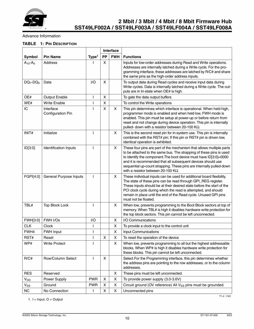
TABLE 1: PIN DESCRIPTION
Symbol Pin Name Type1
Interface
FunctionsPP FWH
A10-A0 Address I X Inputs for low-order addresses during Read and Write operations. Addresses are internally latched during a Write cycle. For the pro-gramming interface, these addresses are latched by R/C# and share the same pins as the high-order address inputs.
DQ7-DQ0 Data I/O X To output data during Read cycles and receive input data during Write cycles. Data is internally latched during a Write cycle. The out-puts are in tri-state when OE# is high.
OE# Output Enable I X To gate the data output buffers
WE# Write Enable I X To control the Write operations
IC Interface Configuration Pin
I X X This pin determines which interface is operational. When held high, programmer mode is enabled and when held low, FWH mode is enabled. This pin must be setup at power-up or before return from reset and not change during device operation. This pin is internally pulled- down with a resistor between 20-100 KΩ.
INIT# Initialize I X This is the second reset pin for in-system use. This pin is internally combined with the RST# pin; If this pin or RST# pin is driven low, identical operation is exhibited.
ID[3:0] Identification Inputs I X These four pins are part of the mechanism that allows multiple parts to be attached to the same bus. The strapping of these pins is used to identify the component.The boot device must have ID[3:0]=0000 and it is recommended that all subsequent devices should use sequential up-count strapping. These pins are internally pulled-down with a resistor between 20-100 KΩ.
FGPI[4:0] General Purpose Inputs I X These individual inputs can be used for additional board flexibility. The state of these pins can be read through GPI_REG register. These inputs should be at their desired state before the start of the PCI clock cycle during which the read is attempted, and should remain in place until the end of the Read cycle. Unused GPI pins must not be floated.
TBL# Top Block Lock I X When low, prevents programming to the Boot Block sectors at top of memory. When TBL# is high it disables hardware write protection for the top block sectors. This pin cannot be left unconnected.
FWH[3:0] FWH I/Os I/O X I/O Communications
CLK Clock I X To provide a clock input to the control unit
FWH4 FWH Input I X Input Communications
RST# Reset I X X To reset the operation of the device
WP# Write Protect I X When low, prevents programming to all but the highest addressable blocks. When WP# is high it disables hardware write protection for these blocks. This pin cannot be left unconnected.
R/C# Row/Column Select I X Select For the Programming interface, this pin determines whether the address pins are pointing to the row addresses, or to the column addresses.
RES Reserved X These pins must be left unconnected.
VDD Power Supply PWR X X To provide power supply (3.0-3.6V)
VSS Ground PWR X X Circuit ground (OV reference) All VSS pins must be grounded.
NC No Connection I X X Unconnected pinsT1.4 1161
1. I = Input, O = Output
Advance Information
2 Mbit / 3 Mbit / 4 Mbit / 8 Mbit Firmware HubSST49LF002A / SST49LF003A / SST49LF004A / SST49LF008A
11©2003 Silicon Storage Technology, Inc. S71161-07-000 6/03
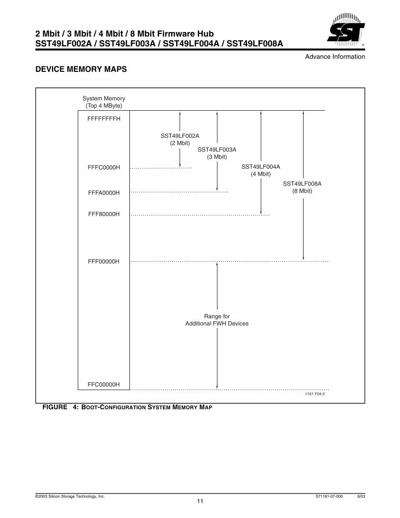
DEVICE MEMORY MAPS
FIGURE 4: BOOT-CONFIGURATION SYSTEM MEMORY MAP
Range forAdditional FWH Devices
FFC00000H
FFF00000H
SST49LF004A(4 Mbit)
SST49LF008A(8 Mbit)
FFF80000H
FFFA0000H
FFFC0000H
FFFFFFFFH
SST49LF002A(2 Mbit)
SST49LF003A(3 Mbit)
System Memory(Top 4 MByte)
1161 F04.0
12
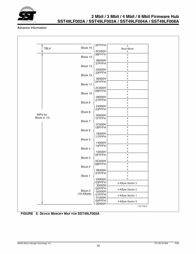
Advance Information
2 Mbit / 3 Mbit / 4 Mbit / 8 Mbit Firmware HubSST49LF002A / SST49LF003A / SST49LF004A / SST49LF008A
©2003 Silicon Storage Technology, Inc. S71161-07-000 6/03
FIGURE 5: DEVICE MEMORY MAP FOR SST49LF002A
3FFFFH
3C000H3BFFFH
38000H37FFFH
34000H33FFFH
30000H2FFFFH
2C000H2BFFFH
28000H27FFFH
24000H23FFFH
20000H1FFFFH
1C000H1BFFFH
18000H17FFFH
14000H13FFFH
10000H0FFFFH
0C000H0BFFFH
08000H07FFFH
04000H03FFFH300000
02FFFH02000H01FFFH01000H00FFFH00000H
Block 7
Block 8
Block 6
Block 5
Block 4
Block 3
Block 2
Block 1
Block 15
Block 14
Block 13
Block 12
Block 11
Block 10
Block 9
Block 0(16 KByte)
1161 F05.0
WP# for Block 0~14
TBL#
4 KByte Sector 1
4 KByte Sector 2
4 KByte Sector 3
4 KByte Sector 0
Boot Block
Advance Information
2 Mbit / 3 Mbit / 4 Mbit / 8 Mbit Firmware HubSST49LF002A / SST49LF003A / SST49LF004A / SST49LF008A
13©2003 Silicon Storage Technology, Inc. S71161-07-000 6/03
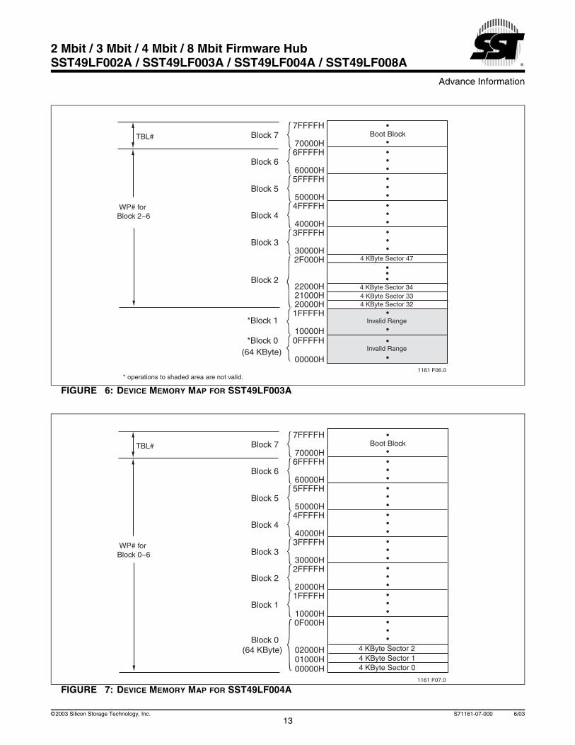
FIGURE 6: DEVICE MEMORY MAP FOR SST49LF003A
FIGURE 7: DEVICE MEMORY MAP FOR SST49LF004A
7FFFFH
70000H6FFFFH
60000H5FFFFH
50000H4FFFFH
40000H3FFFFH
30000H2F000H
22000H21000H20000H1FFFFH
10000H0FFFFH
00000H
Block 7
Block 6
Block 5
Block 4
Block 3
Block 2
*Block 1
4 KByte Sector 334 KByte Sector 34
4 KByte Sector 32
Invalid Range
Invalid Range
4 KByte Sector 47
*Block 0
1161 F06.0
(64 KByte)
Boot Block
* operations to shaded area are not valid.
WP# for Block 2~6
TBL#
7FFFFH
70000H6FFFFH
60000H5FFFFH
50000H4FFFFH
40000H3FFFFH
30000H2FFFFH
20000H1FFFFH
10000H0F000H
02000H01000H00000H
4 KByte Sector 14 KByte Sector 2
4 KByte Sector 0
Block 7
Block 6
Block 5
Block 4
Block 3
Block 2
Block 1
Block 0
1161 F07.0
(64 KByte)
Boot Block
WP# for Block 0~6
TBL#
14
Advance Information
2 Mbit / 3 Mbit / 4 Mbit / 8 Mbit Firmware HubSST49LF002A / SST49LF003A / SST49LF004A / SST49LF008A
©2003 Silicon Storage Technology, Inc. S71161-07-000 6/03
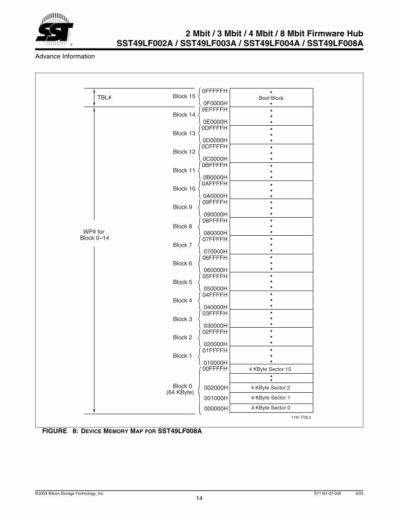
FIGURE 8: DEVICE MEMORY MAP FOR SST49LF008A
0FFFFFH
0F0000H0EFFFFH
0E0000H0DFFFFH
0D0000H0CFFFFH
0C0000H0BFFFFH
0B0000H0AFFFFH
0A0000H09FFFFH
090000H08FFFFH
080000H07FFFFH
070000H06FFFFH
060000H05FFFFH
050000H04FFFFH
040000H03FFFFH
030000H02FFFFH
020000H01FFFFH
010000H00FFFFH
Block 7
Block 8
Block 6
Block 5
Block 4
Block 3
Block 2
Block 1
Block 15
Block 14
Block 13
Block 12
Block 11
Block 10
Block 9
Block 0(64 KByte)
1161 F08.0
WP# for Block 0~14
TBL#
4 KByte Sector 1
4 KByte Sector 2
4 KByte Sector 15
4 KByte Sector 0
Boot Block
002000H
001000H
000000H
Advance Information
2 Mbit / 3 Mbit / 4 Mbit / 8 Mbit Firmware HubSST49LF002A / SST49LF003A / SST49LF004A / SST49LF008A
15©2003 Silicon Storage Technology, Inc. S71161-07-000 6/03
DESIGN CONSIDERATIONS
SST recommends a high frequency 0.1 µF ceramic capacitorto be placed as close as possible between VDD and VSS lessthan 1 cm away from the VDD pin of the device. Additionally, alow frequency 4.7 µF electrolytic capacitor from VDD to VSSshould be placed within 1 cm of the VDD pin. If you use asocket for programming purposes add an additional 1-10 µFnext to each socket.
The RST# pin must remain stable at VIH for the entire dura-tion of an Erase operation. WP# must remain stable at VIH forthe entire duration of the Erase and Program operations fornon-Boot Block sectors. To write data to the top Boot Blocksectors, the TBL# pin must also remain stable at VIH for theentire duration of the Erase and Program operations.
PRODUCT IDENTIFICATION
The product identification mode identifies the device as theSST49LF00xA and manufacturer as SST.
MODE SELECTION
The SST49LF00xA flash memory devices can operate intwo distinct interface modes: the Firmware Hub Interface(FWH) mode and the Parallel Programming (PP) mode.The IC (Interface Configuration pin) is used to set theinterface mode selection. If the IC pin is set to logic High,the device is in PP mode; while if the IC pin is set Low,the device is in the FWH mode. The IC selection pin mustbe configured prior to device operation. The IC pin is
internally pulled down if the pin is not connected. In FWHmode, the device is configured to interface with its hostusing Intel’s Firmware Hub proprietary protocol. Commu-nication between Host and the SST49LF00xA occurs viathe 4-bit I/O communication signals, FWH [3:0] and theFWH4. In PP mode, the device is programmed via an 11-bit address and an 8-bit data I/O parallel signals. Theaddress inputs are multiplexed in row and columnselected by control signal R/C# pin. The columnaddresses are mapped to the higher internal addresses,and the row addresses are mapped to the lower internaladdresses. See the Device Memory Maps in Figures 5through 8 for address assignments.
FIRMWARE HUB (FWH) MODE
Device OperationThe FWH mode uses a 5-signal communication interface,FWH[3:0] and FWH4, to control operations of theSST49LF00xA. Operations such as Memory Read andMemory Write uses Intel FWH propriety protocol. JEDECStandard SDP (Software Data Protection) Byte-Program,Sector-Erase and Block-Erase command sequences areincorporated into the FWH memory cycles. Chip-Erase isonly available in PP Mode.
The device enters standby mode when FWH4 is high andno internal operation is in progress. The device is in readymode when FWH4 is low and no activity is on the FWH bus.
Firmware Hub Interface CyclesAddresses and data are transferred to and from theSST49LF00xA by a series of “fields,” where each field con-tains 4 bits of data. ST49LF00xA supports only single-byteread and writes, and all fields are one clock cycle in length.Field sequences and contents are strictly defined for Readand Write operations. Addresses in this section refer toaddresses as seen from the SST49LF00xA’s “point ofview,” some calculation will be required to translate these tothe actual locations in the memory map (and vice versa) ifmultiple memory device is used on the bus. Tables 3 and 4list the field sequences for Read and Write cycles.
TABLE 2: PRODUCT IDENTIFICATION
Byte Data
JEDEC IDAddressLocation
Manufacturer’s ID 0000H BFH FFBC0000H
Device ID
SST49LF002A 0001H 57H FFBC0001H
SST49LF003A 0001H 1BH FFBC0001H
SST49LF004A 0001H 60H FFBC0001H
SST49LF008A 0001H 5AH FFBC0001HT2.5 1161
16
Advance Information
2 Mbit / 3 Mbit / 4 Mbit / 8 Mbit Firmware HubSST49LF002A / SST49LF003A / SST49LF004A / SST49LF008A
©2003 Silicon Storage Technology, Inc. S71161-07-000 6/03
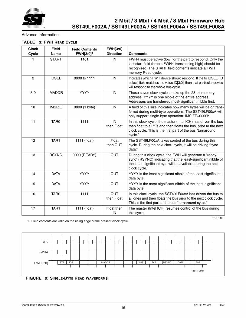
FIGURE 9: SINGLE-BYTE READ WAVEFORMS
TABLE 3: FWH READ CYCLE
ClockCycle
FieldName
Field Contents FWH[3:0]1
FWH[3:0]Direction Comments
1 START 1101 IN FWH4 must be active (low) for the part to respond. Only the last start field (before FWH4 transitioning high) should be recognized. The START field contents indicate a FWH memory Read cycle.
2 IDSEL 0000 to 1111 IN Indicates which FWH device should respond. If the to IDSEL (ID select) field matches the value ID[3:0], then that particular device will respond to the whole bus cycle.
3-9 IMADDR YYYY IN These seven clock cycles make up the 28-bit memory address. YYYY is one nibble of the entire address. Addresses are transferred most-significant nibble first.
10 IMSIZE 0000 (1 byte) IN A field of this size indicates how many bytes will be or trans-ferred during multi-byte operations. The SST49LF00xA will only support single-byte operation. IMSIZE=0000b
11 TAR0 1111 INthen Float
In this clock cycle, the master (Intel ICH) has driven the bus then float to all ‘1’s and then floats the bus, prior to the next clock cycle. This is the first part of the bus “turnaround cycle.”
12 TAR1 1111 (float) Float then OUT
The SST49LF00xA takes control of the bus during this cycle. During the next clock cycle, it will be driving “sync data.”
13 RSYNC 0000 (READY) OUT During this clock cycle, the FWH will generate a “ready-sync” (RSYNC) indicating that the least-significant nibble of the least-significant byte will be available during the next clock cycle.
14 DATA YYYY OUT YYYY is the least-significant nibble of the least-significant data byte.
15 DATA YYYY OUT YYYY is the most-significant nibble of the least-significant data byte.
16 TAR0 1111 OUT then Float
In this clock cycle, the SST49LF00xA has driven the bus to all ones and then floats the bus prior to the next clock cycle. This is the first part of the bus “turnaround cycle.”
17 TAR1 1111 (float) Float thenIN
The master (Intel ICH) resumes control of the bus during this cycle.
T3.3 11611. Field contents are valid on the rising edge of the present clock cycle.
CLK
FWH4
FWH[3:0]
1161 F09.0
STR TAR RSYNCIMSIMADDRIDS DATA TAR
Advance Information
2 Mbit / 3 Mbit / 4 Mbit / 8 Mbit Firmware HubSST49LF002A / SST49LF003A / SST49LF004A / SST49LF008A
17©2003 Silicon Storage Technology, Inc. S71161-07-000 6/03
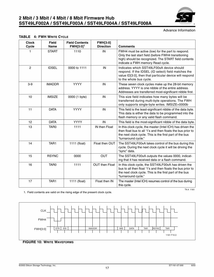
FIGURE 10: WRITE WAVEFORMS
TABLE 4: FWH WRITE CYCLE
ClockCycle
FieldName
Field ContentsFWH[3:0]1
FWH[3:0]Direction Comments
1 START 1110 IN FWH4 must be active (low) for the part to respond. Only the last start field (before FWH4 transitioning high) should be recognized. The START field contents indicate a FWH memory Read cycle.
2 IDSEL 0000 to 1111 IN Indicates which SST49LF00xA device should respond. If the IDSEL (ID select) field matches the value ID[3:0], then that particular device will respond to the whole bus cycle.
3-9 IMADDR YYYY IN These seven clock cycles make up the 28-bit memory address. YYYY is one nibble of the entire address. Addresses are transferred most-significant nibble first.
10 IMSIZE 0000 (1 byte) IN This size field indicates how many bytes will be transferred during multi-byte operations. The FWH only supports single-byte writes. IMSIZE=0000b
11 DATA YYYY IN This field is the least-significant nibble of the data byte. This data is either the data to be programmed into the flash memory or any valid flash command.
12 DATA YYYY IN This field is the most-significant nibble of the data byte.
13 TAR0 1111 IN then Float In this clock cycle, the master (Intel ICH) has driven the then float bus to all ‘1’s and then floats the bus prior to the next clock cycle. This is the first part of the bus “turnaround cycle.”
14 TAR1 1111 (float) Float then OUT The SST49LF00xA takes control of the bus during this cycle. During the next clock cycle it will be driving the “sync” data.
15 RSYNC 0000 OUT The SST49LF00xA outputs the values 0000, indicat-ing that it has received data or a flash command.
16 TAR0 1111 OUT then Float In this clock cycle, the SST49LF00xA has driven the bus to all then float ‘1’s and then floats the bus prior to the next clock cycle. This is the first part of the bus “turnaround cycle.”
17 TAR1 1111 (float) Float then IN The master (Intel ICH) resumes control of the bus during this cycle.
T4.4 11611. Field contents are valid on the rising edge of the present clock cycle.
CLK
FWH4
FWH[3:0]
1161 F10.0
STR DATA TARTAR RSYNCIMSIMADDRIDS
18
Advance Information
2 Mbit / 3 Mbit / 4 Mbit / 8 Mbit Firmware HubSST49LF002A / SST49LF003A / SST49LF004A / SST49LF008A
©2003 Silicon Storage Technology, Inc. S71161-07-000 6/03
Abort MechanismIf FWH4 is driven low for one or more clock cycles during aFWH cycle, the cycle will be terminated and the device willwait for the ABORT command. The host may drive theFWH[3:0] with ‘1111b’ (ABORT command) to return thedevice to Ready mode. If abort occurs during a Write oper-ation, the data may be incorrectly altered.
Response To Invalid FieldsDuring FWH operations, the FWH will not explicitly indicatethat it has received invalid field sequences. The responseto specific invalid fields or sequences is as follows:
Address out of range: The FWH address sequence is7 fields long (28 bits), but only the last five address fields(20 bits) will be decoded by SST49LF00xA.
Address A22 has the special function of directing reads andwrites to the flash core (A22=1) or to the register space(A22=0).
The SST49LF003A features are equivalent to theSST49LF004A with 128 KByte less memory. For theSST49LF003A, operations beyond the 3-Mbit boundary(below 20000H) are not valid (see Device Memory Map).
Invalid IMSIZE field: If the FWH receives an invalid sizefield during a Read or Write operation, the device will resetand no operation will be attempted. The SST49LF00xA willnot generate any kind of response in this situation. Invalid-size fields for a Read/Write cycle are anything but 0000b.
Device Memory Hardware Write ProtectionThe Top Boot Lock (TBL#) and Write Protect (WP#) pinsare provided for hardware write protection of devicememory in the SST49LF00xA. The TBL# pin is used towrite protect 16 boot sectors (64 KByte) at the highestflash memory address range for the SST49LF003A/004A/008A and 4 boot sectors (16 KByte) forSST49LF002A. WP# pin write protects the remainingsectors in the flash memory.
An active low signal at the TBL# pin prevents Program andErase operations of the top boot sectors. When TBL# pin isheld high, write protection of the top boot sectors is thendetermined by the Boot Block Locking register. The WP#pin serves the same function for the remaining sectors ofthe device memory. The TBL# and WP# pins write protec-tion functions operate independently of one another.
Both TBL# and WP# pins must be set to their requiredprotection states prior to starting a Program or Eraseoperation. A logic level change occurring at the TBL# or
WP# pin during a Program or Erase operation couldcause unpredictable results. TBL# and WP# pins cannotbe left unconnected.
TBL# is internally OR’ed with the top Boot Block Lockingregister. When TBL# is low, the top Boot Block is hard-ware write protected regardless of the state of the Write-Lock bit for the Boot Block Locking register. Clearing theWrite-Protect bit in the register when TBL# is low will haveno functional effect, even though the register may indicatethat the block is no longer locked.
WP# is internally OR’ed with the Block Locking register.When WP# is low, the blocks are hardware write pro-tected regardless of the state of the Write-Lock bit for thecorresponding Block Locking registers. Clearing theWrite-Protect bit in any register when WP# is low will haveno functional effect, even though the register may indicatethat the block is no longer locked.
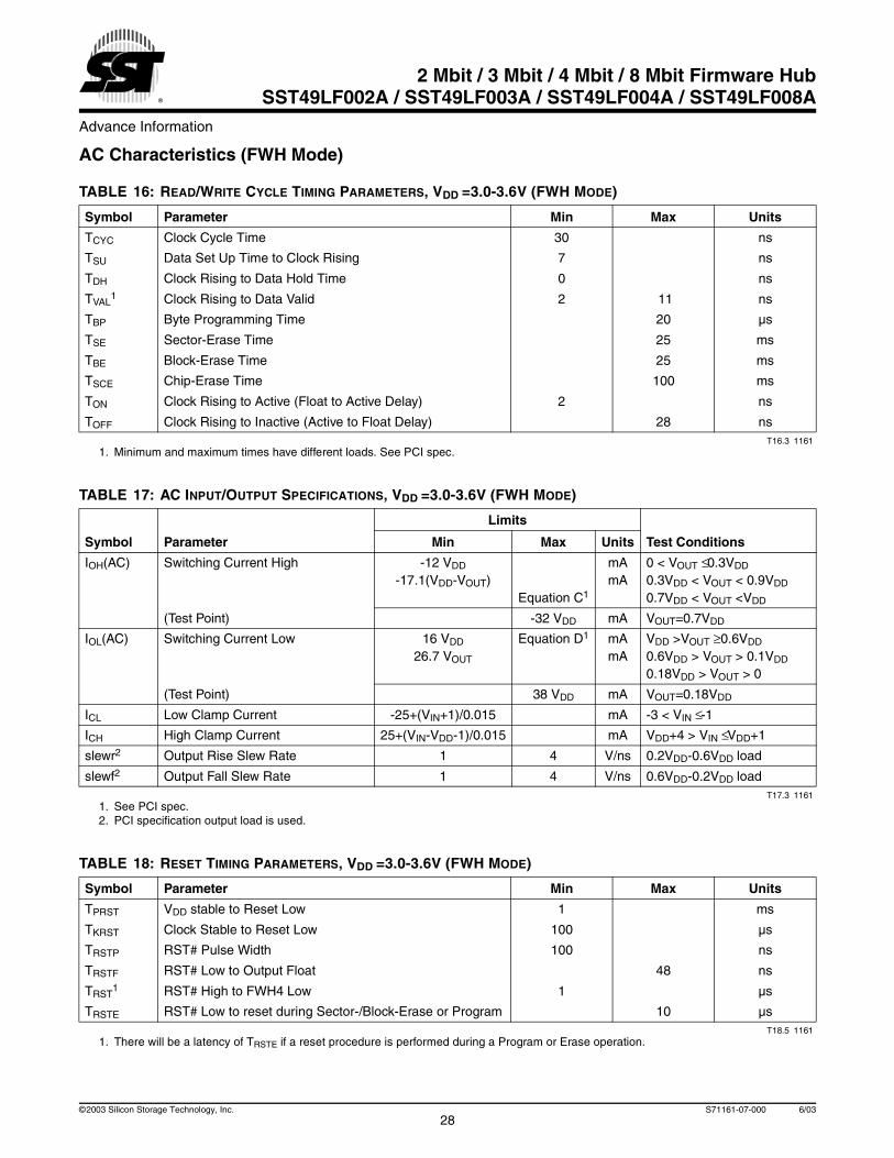
ResetA VIL on INIT# or RST# pin initiates a device reset. INIT#and RST# pins have the same function internally. It isrequired to drive INIT# or RST# pins low during a systemreset to ensure proper CPU initialization.
During a Read operation, driving INIT# or RST# pins lowdeselects the device and places the output drivers,FWH[3:0], in a high-impedance state. The reset signalmust be held low for a minimal duration of time TRSTP. Areset latency will occur if a reset procedure is performedduring a Program or Erase operation. See Table 18, ResetTiming Parameters for more information. A device resetduring an active Program or Erase will abort the operationand memory contents may become invalid due to databeing altered or corrupted from an incomplete Erase orProgram operation.
Write Operation Status DetectionThe SST49LF00xA device provides two software means todetect the completion of a Write (Program or Erase) cycle,in order to optimize the system Write cycle time. The soft-ware detection includes two status bits: Data# Polling(DQ7) and Toggle Bit (DQ6). The End-of-Write detectionmode is incorporated into the FWH Read cycle. The actualcompletion of the nonvolatile write is asynchronous with thesystem; therefore, either a Data# Polling or Toggle Bit readmay be simultaneous with the completion of the Writecycle. If this occurs, the system may possibly get an errone-ous result, i.e., valid data may appear to conflict with eitherDQ7 or DQ6. In order to prevent spurious rejection, if anerroneous result occurs, the software routine should
Advance Information
2 Mbit / 3 Mbit / 4 Mbit / 8 Mbit Firmware HubSST49LF002A / SST49LF003A / SST49LF004A / SST49LF008A
19©2003 Silicon Storage Technology, Inc. S71161-07-000 6/03
include a loop to read the accessed location an additionaltwo (2) times. If both reads are valid, then the device hascompleted the Write cycle, otherwise the rejection is valid.
Data# Polling (DQ7)When the SST49LF00xA device is in the internal Programoperation, any attempt to read DQ7 will produce the com-plement of the true data. Once the Program operation iscompleted, DQ7 will produce true data. Note that eventhough DQ7 may have valid data immediately following thecompletion of an internal Write operation, the remainingdata outputs may still be invalid: valid data on the entiredata bus will appear in subsequent successive Readcycles after an interval of 1 µs. During internal Erase opera-tion, any attempt to read DQ7 will produce a ‘0’. Once theinternal Erase operation is completed, DQ7 will produce a‘1’. Proper status will not be given using Data# Polling if theaddress is in the invalid range.
Toggle Bit (DQ6)During the internal Program or Erase operation, any con-secutive attempts to read DQ6 will produce alternating‘0’s and ‘1’s, i.e., toggling between 0 and 1. When theinternal Program or Erase operation is completed, thetoggling will stop.
Multiple Device SelectionThe four ID pins, ID[3:0], allow multiple devices to beattached to the same bus by using different ID strapping ina system. When the SST49LF00xA is used as a bootdevice, ID[3:0] must be strapped as 0000, all subsequentdevices should use a sequential up-count strapping (i.e.0001, 0010, 0011, etc.). The SST49LF00xA will comparethe strapping values, if there is a mismatch, the device willignore the remainder of the cycle and go into standbymode. For further information regarding FWH device map-ping and paging, please refer to the Intel 82801(ICH) I/OController Hub documentation. Since there is no ID supportin PP Mode, to program multiple devices a stand-alonePROM programmer is recommended.
REGISTERS
There are three types of registers available on theSST49LF00xA, the General Purpose Inputs register, BlockLocking registers and the JEDEC ID registers. These regis-ters appear at their respective address location in the 4GByte system memory map. Unused register locations willread as 00H. Attempts to read or write to any registers dur-ing internal Write operations will be ignored.
General Purpose Inputs RegisterThe GPI_REG (General Purpose Inputs Register) passesthe state of FGPI[4:0] pins at power-up on theSST49LF00xA. It is recommended that the FGPI[4:0] pinsare in the desired state before FWH4 is brought low for thebeginning of the bus cycle, and remain in that state until theend of the cycle. There is no default value since this is apass-through register. The GPI register for the boot deviceappears at FFBC0100H in the 4 GByte system memorymap, and will appear elsewhere if the device is not the bootdevice. Register is not available for read when the device isin Erase/Program operation. See Table 5 for the GPI_REGbits and function.
Block Locking RegistersSST49LF00xA provides software controlled lock pro-tection through a set of Block Locking registers. TheBlock Locking Registers are read/write registers and itis accessible through standard addressable memorylocations specified in Table 6 and Table 7. Unused reg-ister locations will read as 00H.
TABLE 5: GENERAL PURPOSE INPUTS REGISTER
Bit Function
Pin #
32-PLCC 32-TSOP
7:5 Reserved - -
4 FGPI[4]Reads status of generalpurpose input pin
30 6
3 FGPI[3]Reads status of generalpurpose input pin
3 11
2 FGPI[2]Reads status of generalpurpose input pin
4 12
1 FGPI[1]Reads status of generalpurpose input pin
5 13
0 FGPI[0]Reads status of generalpurpose input pin
6 14
T5.2 1161
20
Advance Information
2 Mbit / 3 Mbit / 4 Mbit / 8 Mbit Firmware HubSST49LF002A / SST49LF003A / SST49LF004A / SST49LF008A
©2003 Silicon Storage Technology, Inc. S71161-07-000 6/03
TABLE 6: BLOCK LOCKING REGISTERS FOR SST49LF002A1
Register Block SizeProtected MemoryAddress Package
Memory MapRegister Address
T_BLOCK_LK 16K 3FFFFH - 3C000H FFBF8002H
T_MINUS01_LK 16K16K16K
3BFFFH - 38000H37FFFH - 34000H33FFFH - 30000H
FFBF0002H
T_MINUS02_LK 16K16K
2FFFFH - 2C000H2BFFFH - 28000H
FFBE8002H
T_MINUS03_LK 16K16K
27FFFH - 24000H23FFFH - 20000H
FFBE0002H
T_MINUS04_LK 16K16K
1FFFFH - 1C000H1BFFFH - 18000H
FFBD8002H
T_MINUS05_LK 16K16K
17FFFH - 14000H13FFFH - 10000H
FFBD0002H
T_MINUS06_LK 16K16K
0FFFFH - 0C000H0BFFFH - 08000H
FFBC8002H
T_MINUS07_LK 16K16K
07FFFH - 04000H03FFFH - 00000H
FFBC0002H
T6.1 11611. Default value at power up is 01H
TABLE 7: BLOCK LOCKING REGISTERS FOR SST49LF003A/004A/008A1
1. Default value at power up is 01H
RegisterBlockSize
Protected Memory Address Range Memory Map Register AddressSST49LF003A SST49LF004A SST49LF008A
T_BLOCK_LK 64K 07FFFFH - 070000H 07FFFFH - 070000H 0FFFFFH - 0F0000H FFBF0002H
T_MINUS01_LK 64K 06FFFFH - 060000H 06FFFFH - 060000H 0EFFFFH - 0E0000H FFBE0002H
T_MINUS02_LK 64K 05FFFFH - 050000H 05FFFFH - 050000H 0DFFFFH - 0D0000H FFBD0002H
T_MINUS03_LK 64K 04FFFFH - 040000H 04FFFFH - 040000H 0CFFFFH - 0C0000H FFBC0002H
T_MINUS04_LK 64K 03FFFFH - 030000H 03FFFFH - 030000H 0BFFFFH - 0B0000H FFBB0002H
T_MINUS05_LK 64K 02FFFFH - 020000H 02FFFFH - 020000H 0AFFFFH - 0A0000H FFBA0002H
T_MINUS06_LK 64K 01FFFFH - 010000H 09FFFFH - 090000H FFB90002H
T_MINUS07_LK 64K 00FFFFH - 000000H 08FFFFH - 080000H FFB80002H
T_MINUS08_LK 64K 07FFFFH - 070000H FFB70002H
T_MINUS09_LK 64K 06FFFFH - 060000H FFB60002H
T_MINUS10_LK 64K 05FFFFH - 050000H FFB50002H
T_MINUS11_LK 64K 04FFFFH - 040000H FFB40002H
T_MINUS12_LK 64K 03FFFFH - 030000H FFB30002H
T_MINUS13_LK 64K 02FFFFH - 020000H FFB20002H
T_MINUS14_LK 64K 01FFFFH -010000H FFB10002H
T_MINUS15_LK 64K 00FFFFH - 000000H FFB00002HT7.2 1161
Advance Information
2 Mbit / 3 Mbit / 4 Mbit / 8 Mbit Firmware HubSST49LF002A / SST49LF003A / SST49LF004A / SST49LF008A
21©2003 Silicon Storage Technology, Inc. S71161-07-000 6/03
Write LockThe Write-Lock bit, bit 0, controls the lock state described inTable 8. The default Write status of all blocks after power-up is write locked. When bit 0 of the Block Locking registeris set, Program and Erase operations for the correspondingblock are prevented. Clearing the Write-Lock bit will unpro-tect the block. The Write-Lock bit must be cleared prior tostarting a Program or Erase operation since it is sampled atthe beginning of the operation.
The Write-Lock bit functions in conjunction with the hard-ware Write Lock pin TBL# for the top Boot Block. WhenTBL# is low, it overrides the software locking scheme. Thetop Boot Block Locking register does not indicate the stateof the TBL# pin.
The Write-Lock bit functions in conjunction with the hard-ware WP# pin for blocks 0 to 6. When WP# is low, it over-rides the software locking scheme. The Block Lockingregister does not indicate the state of the WP# pin.
Lock DownThe Lock-Down bit, bit 1, controls the Block Locking regis-ter as described in Table 8. When in the FWH interfacemode, the default Lock Down status of all blocks uponpower-up is not locked down. Once the Lock-Down bit isset, any future attempted changes to that Block Lockingregister will be ignored. The Lock-Down bit is only clearedupon a device reset with RST# or INIT# or power down.Current Lock Down status of a particular block can bedetermined by reading the corresponding Lock-Down bit.Once a block’s Lock-Down bit is set, the Write-Lock bits forthat block can no longer be modified, and the block islocked down in its current state of write accessibility.
JEDEC ID RegistersThe JEDEC ID registers for the boot device appear atFFBC0000H and FFBC0001H in the 4 GByte systemmemory map, and will appear elsewhere if the device is notthe boot device. Register is not available for read when thedevice is in Erase/Program operation. Unused registerlocation will read as 00H. Refer to the relevant applicationnote for details. See Table 2 for the device ID code.
PARALLEL PROGRAMMING MODE
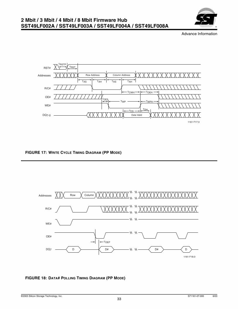
Device OperationCommands are used to initiate the memory operation func-tions of the device. The data portion of the software com-mand sequence is latched on the rising edge of WE#.During the software command sequence the row addressis latched on the falling edge of R/C# and the columnaddress is latched on the rising edge of R/C#.
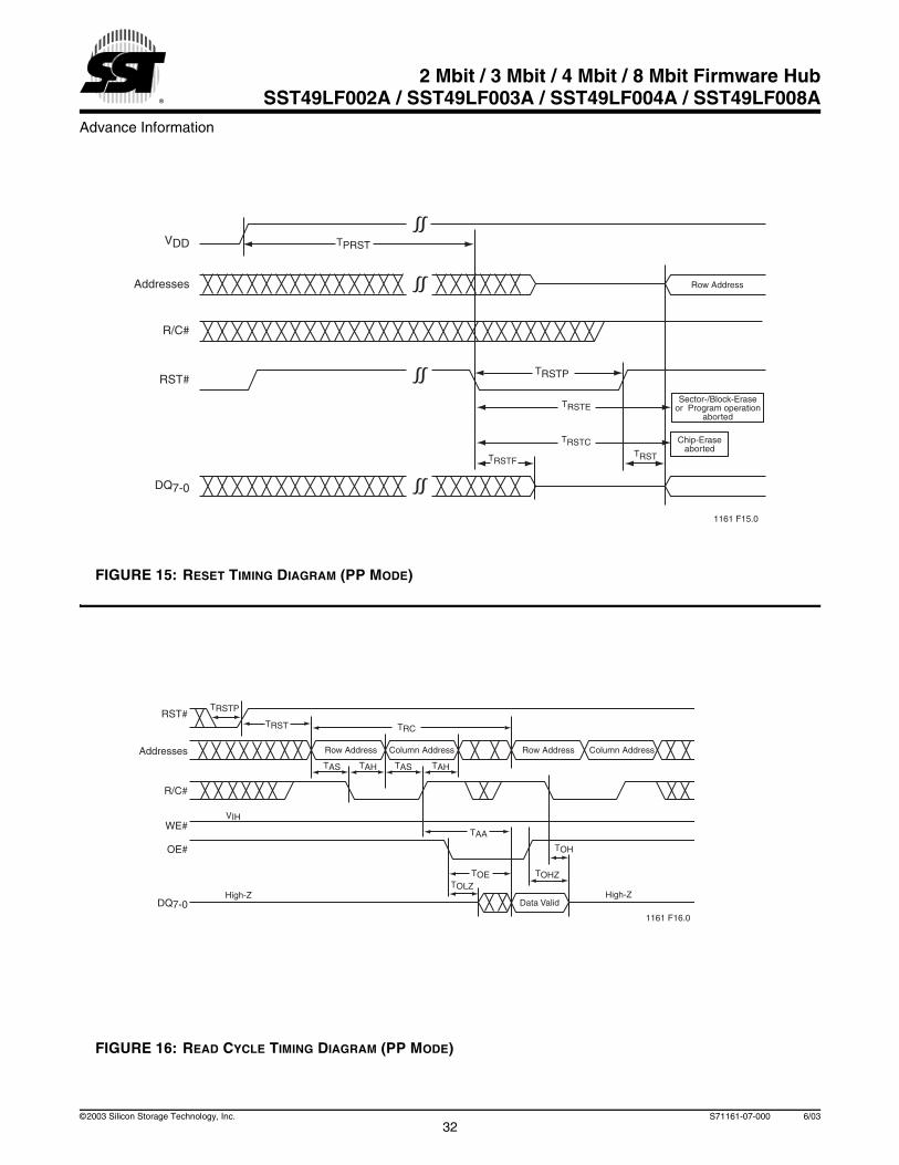
ResetA VIL on RST# pin initiates a device reset.
ReadThe Read operation of the SST49LF00xA device is con-trolled by OE#. OE# is the output control and is used togate data from the output pins. Refer to the Read cycletiming diagram, Figure 16, for further details.
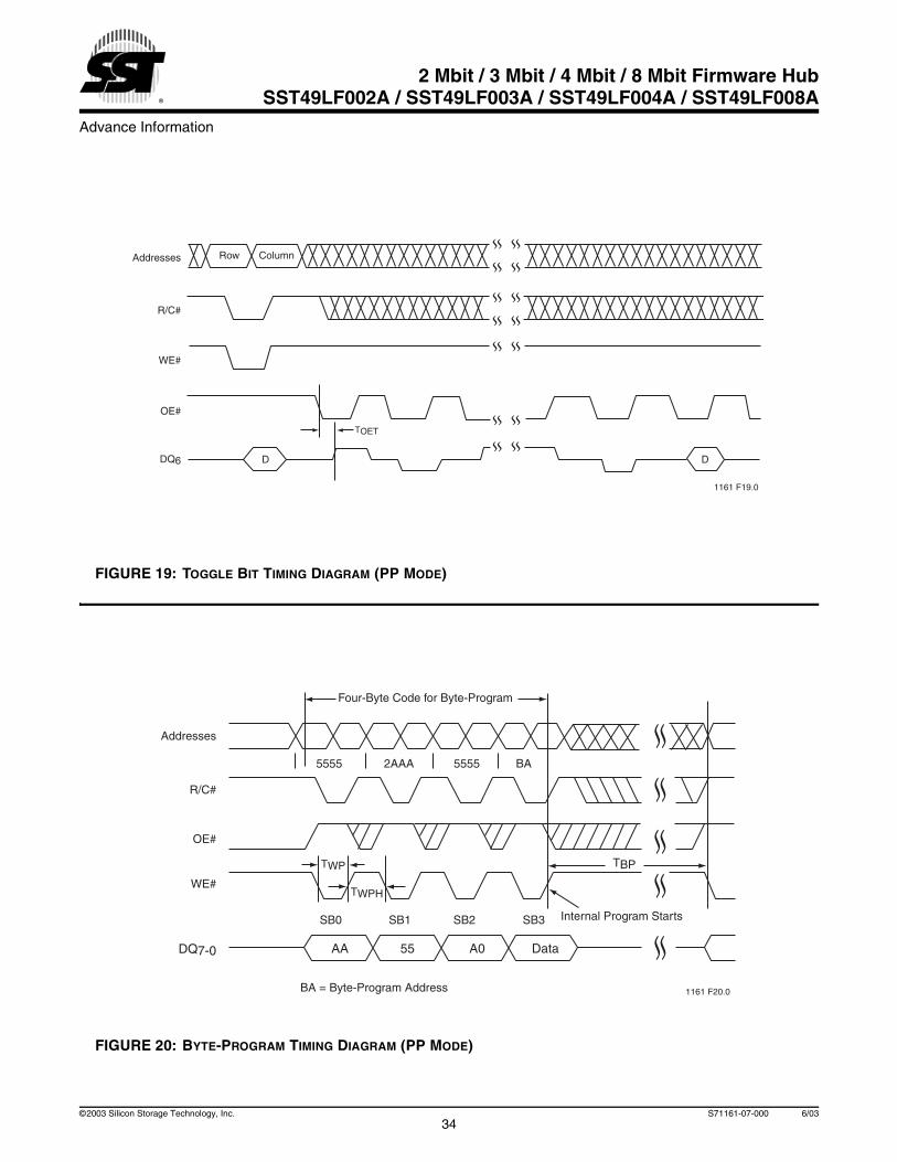
Byte-Program OperationThe SST49LF00xA device is programmed on a byte-by-byte basis. Before programming, one must ensure that thesector, in which the byte which is being programmed exists,is fully erased. The Byte-Program operation is initiated byexecuting a four-byte command load sequence for Soft-ware Data Protection with address (BA) and data in the lastbyte sequence. During the Byte-Program operation, therow address (A10-A0) is latched on the falling edge of R/C#and the column Address (A21-A11) is latched on the risingedge of R/C#. The data bus is latched in the rising edge ofWE#. The Program operation, once initiated, will be com-pleted, within 20 µs. See Figure 17 for Program operationtiming diagram, Figure 20 for timing waveforms, and Figure28 for its flowchart. During the Program operation, the onlyvalid reads are Data# Polling and Toggle Bit. During theinternal Program operation, the host is free to perform addi-tional tasks. Any commands written during the internal Pro-gram operation will be ignored.
TABLE 8: BLOCK LOCKING REGISTER BITS
Reserved Bit [7..2] Lock-Down Bit [1] Write-Lock Bit [0] Lock Status000000 0 0 Full Access000000 0 1 Write Locked (Default State at Power-Up)000000 1 0 Locked Open (Full Access Locked Down)
000000 1 1 Write Locked DownT8.3 1161
22
Advance Information
2 Mbit / 3 Mbit / 4 Mbit / 8 Mbit Firmware HubSST49LF002A / SST49LF003A / SST49LF004A / SST49LF008A
©2003 Silicon Storage Technology, Inc. S71161-07-000 6/03
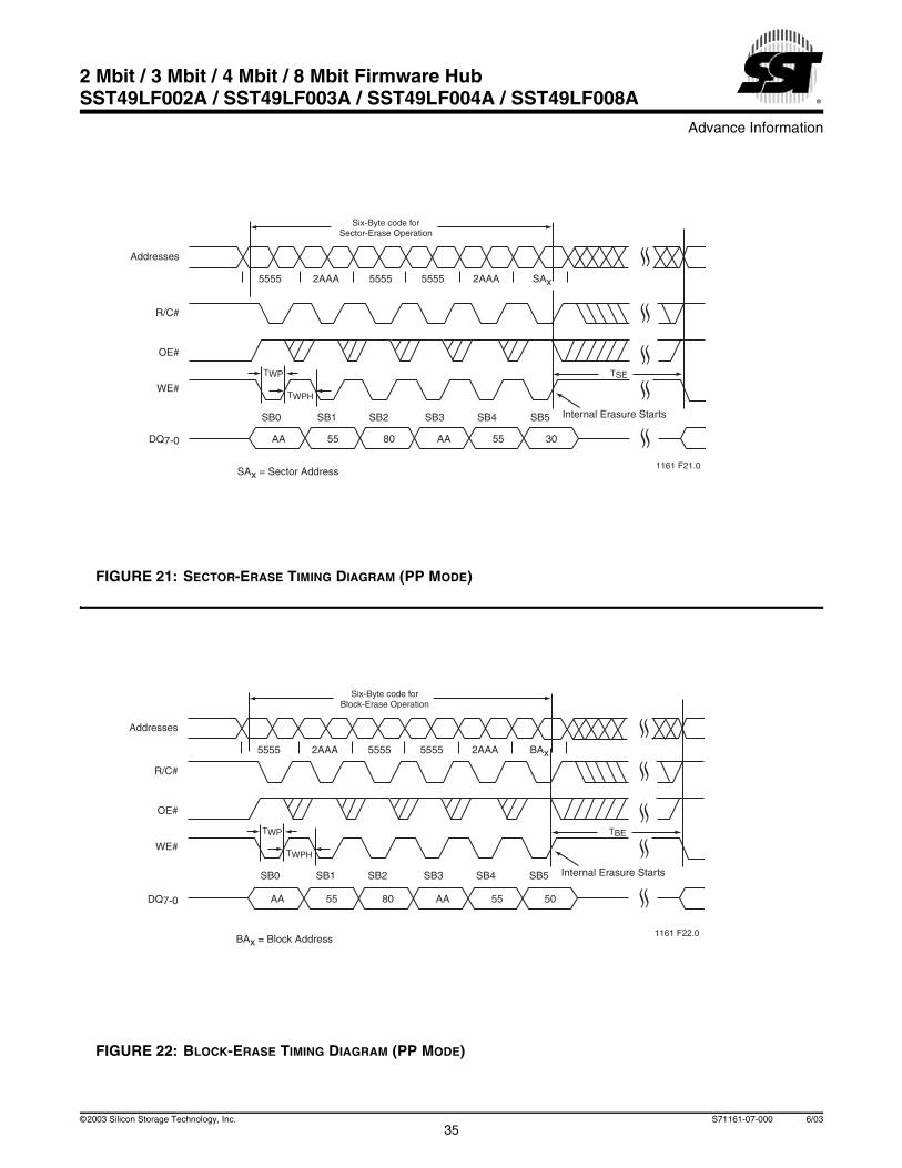
Sector-Erase OperationThe Sector-Erase operation allows the system to erase thedevice on a sector-by-sector basis. The sector architectureis based on uniform sector size of 4 KByte. The Sector-Erase operation is initiated by executing a six-byte com-mand load sequence for Software Data Protection withSector-Erase command (30H) and sector address (SA) inthe last bus cycle. The internal Erase operation begins afterthe sixth WE# pulse. The End-of-Erase can be determinedusing either Data# Polling or Toggle Bit methods. See Fig-ure 21 for Sector-Erase timing waveforms. Any commandswritten during the Sector-Erase operation will be ignored.
Block-Erase OperationThe Block-Erase Operation allows the system to erasethe device in 64 KByte uniform block size for theSST49LF003A/SST49LF004A/SST49LF008A and 16KByte uniform block size for the SST49LF002A. TheBlock-Erase operation is initiated by executing a six-bytecommand load sequence for Software Data Protectionwith Block-Erase command (50H) and block address.The internal Block-Erase operation begins after the sixthWE# pulse. The End-of-Erase can be determined usingeither Data# Polling or Toggle Bit methods. See Figure22 for timing waveforms. Any commands written duringthe Block-Erase operation will be ignored.
Chip-EraseThe SST49LF00xA device provides a Chip-Erase opera-tion only in PP Mode, which allows the user to erase theentire memory array to the ‘1’s state. This is useful whenthe entire device must be quickly erased.
The Chip-Erase operation is initiated by executing a six-byte Software Data Protection command sequence withChip-Erase command (10H) with address 5555H in the lastbyte sequence. The internal Erase operation begins withthe rising edge of the sixth WE#. During the internal Eraseoperation, the only valid read is Toggle Bit or Data# Polling.See Table 10 for the command sequence, Figure 23 fortiming diagram, and Figure 31 for the flowchart. Any com-mands written during the Chip-Erase operation will beignored.
Write Operation Status DetectionThe SST49LF00xA device provides two software meansto detect the completion of a Write (Program or Erase)cycle, in order to optimize the system Write cycle time. Thesoftware detection includes two status bits: Data# Polling(DQ7) and Toggle Bit (DQ6). The End-of-Write detectionmode is enabled after the rising edge of WE# which ini-tiates the internal Program or Erase operation.
The actual completion of the nonvolatile write is asynchro-nous with the system; therefore, either a Data# Polling or Tog-gle Bit read may be simultaneous with the completion of theWrite cycle. If this occurs, the system may possibly get anerroneous result, i.e., valid data may appear to conflict witheither DQ7 or DQ6. In order to prevent spurious rejection, if anerroneous result occurs, the software routine should include aloop to read the accessed location an additional two (2) times.If both reads are valid, then the device has completed theWrite cycle, otherwise the rejection is valid.
Data# Polling (DQ7)
When the SST49LF00xA device is in the internal Programoperation, any attempt to read DQ7 will produce the com-plement of the true data. Once the Program operation iscompleted, DQ7 will produce true data. Note that eventhough DQ7 may have valid data immediately following thecompletion of an internal Write operation, the remainingdata outputs may still be invalid: valid data on the entiredata bus will appear in subsequent successive Readcycles after an interval of 1 µs. During internal Erase opera-tion, any attempt to read DQ7 will produce a ‘0’. Once theinternal Erase operation is completed, DQ7 will produce a‘1’. The Data# Polling is valid after the rising edge of fourthWE# pulse for Program operation. For Sector- or Chip-Erase, the Data# Polling is valid after the rising edge ofsixth WE# pulse. See Figure 18 for Data# Polling timingdiagram and Figure 29 for a flowchart. Proper status willnot be given using Data# Polling if the address is in theinvalid range.
Toggle Bit (DQ6)
During the internal Program or Erase operation, any con-secutive attempts to read DQ6 will produce alternating ‘0’sand ‘1’s, i.e., toggling between 0 and 1. When the internalProgram or Erase operation is completed, the toggling willstop. The device is then ready for the next operation. TheToggle Bit is valid after the rising edge of fourth WE# pulsefor Program operation. For Sector-, Block- or Chip-Erase,the Toggle Bit is valid after the rising edge of sixth WE#pulse. See Figure 19 for Toggle Bit timing diagram and Fig-ure 29 for a flowchart.
Advance Information
2 Mbit / 3 Mbit / 4 Mbit / 8 Mbit Firmware HubSST49LF002A / SST49LF003A / SST49LF004A / SST49LF008A
23©2003 Silicon Storage Technology, Inc. S71161-07-000 6/03
Data ProtectionThe SST49LF00xA device provides both hardware andsoftware features to protect nonvolatile data from inadvert-ent writes.
Hardware Data Protection
Noise/Glitch Protection: A WE# pulse of less than 5 ns willnot initiate a Write cycle.
VDD Power Up/Down Detection: The Write operation isinhibited when VDD is less than 1.5V.
Write Inhibit Mode: Forcing OE# low, WE# high will inhibitthe Write operation. This prevents inadvertent writes duringpower-up or power-down.
Software Data Protection (SDP)
The SST49LF00xA provides the JEDEC approved Soft-ware Data Protection scheme for all data alteration opera-tion, i.e., Program and Erase. Any Program operationrequires the inclusion of a series of three-byte sequences.The three-byte load sequence is used to initiate the Pro-gram operation, providing optimal protection from inadvert-ent Write operations, e.g., during the system power-up orpower-down. Any Erase operation requires the inclusion ofa six-byte load sequence. The SST49LF00xA device isshipped with the Software Data Protection permanentlyenabled. See Table 10 for the specific software commandcodes. During SDP command sequence, invalid com-mands will abort the device to Read mode, within TRC.
TABLE 9: OPERATION MODES SELECTION (PP MODE)
Mode RST# OE# WE# DQ Address
Read VIH VIL VIH DOUT AIN
Program VIH VIH VIL DIN AIN
Erase VIH VIH VIL X1 Sector or Block address, XXH for Chip-Erase
Reset VIL X X High Z X
Write Inhibit VIH VIL X High Z/DOUT X
X X VIH High Z/DOUT X
Product Identification VIH VIL VIH Manufacturer’s ID (BFH)Device ID2
A18-A1=VIL, A0=VIL
A18-A1=VIL, A0=VIH T9.5 1161
1. X can be VIL or VIH, but no other value.2. Device ID 57H for SST49LF002A, 1BH for SST49LF003A, 60H for SST49LF004A, and 5AH for SST49LF008A
24
Advance Information
2 Mbit / 3 Mbit / 4 Mbit / 8 Mbit Firmware HubSST49LF002A / SST49LF003A / SST49LF004A / SST49LF008A
©2003 Silicon Storage Technology, Inc. S71161-07-000 6/03
SOFTWARE COMMAND SEQUENCE
TABLE 10: SOFTWARE COMMAND SEQUENCE
Command Sequence1st1
Write Cycle
1. FWH Mode uses consecutive Write cycles to complete a command sequence; PP Mode uses consecutive bus cycles to complete a command sequence.
2nd1
Write Cycle3rd1
Write Cycle4th1
Write Cycle5th1
Write Cycle6th1
Write Cycle
Addr2
2. Address format A14-A0 (Hex), Addresses A21-A15 can be VIL or VIH, but no other value, for the Command sequence in PP Mode.
Data Addr2 Data Addr2 Data Addr2 Data Addr2 Data Addr2 Data
Byte-Program 5555H AAH 2AAAH 55H 5555H A0H BA3
3. BA = Program Byte address
Data
Sector-Erase 5555H AAH 2AAAH 55H 5555H 80H 5555H AAH 2AAAH 55H SAX4
4. SAX for Sector-Erase Address
30H
Block-Erase 5555H AAH 2AAAH 55H 5555H 80H 5555H AAH 2AAAH 55H BAX5
5. BAX for Block-Erase Address
50H
Chip-Erase6
6. Chip-Erase is supported in PP Mode only
5555H AAH 2AAAH 55H 5555H 80H 5555H AAH 2AAAH 55H 5555H 10H
Software ID Entry7,8
7. SST Manufacturer’s ID = BFH, is read with A0=0,With A17-A1 = 0; 49LF002A Device ID = 57H, is read with A0 = 1.With A18-A1 = 0; 49LF003A Device ID = 1BH, is read with A0 = 1.With A18-A1 = 0; 49LF004A Device ID = 60H, is read with A0 = 1.With A19-A1 = 0; 49LF008A Device ID = 5AH, is read with A0 = 1.
8. The device does not remain in Software Product ID mode if powered down.
5555H AAH 2AAAH 55H 5555H 90H
Software ID Exit9
9. Both Software ID Exit operations are equivalent.
XXH F0H
Software ID Exit9 5555H AAH 2AAAH 55H 5555H F0HT10.5 1161
Advance Information
2 Mbit / 3 Mbit / 4 Mbit / 8 Mbit Firmware HubSST49LF002A / SST49LF003A / SST49LF004A / SST49LF008A
25©2003 Silicon Storage Technology, Inc. S71161-07-000 6/03
ELECTRICAL SPECIFICATIONS
The AC and DC specifications for the FWH Interface signals (FWH[3:0], CLK, FWH4, and RST#) as defined in Sec-tion 4.2.2 of the PCI Local Bus Specification, Rev. 2.1. Refer to Table 11 for the DC voltage and current specifica-tions. Refer to the tables on pages 27 through 31 for the AC timing specifications for Clock, Read/Write, and Resetoperations.
Absolute Maximum Stress Ratings (Applied conditions greater than those listed under “Absolute MaximumStress Ratings” may cause permanent damage to the device. This is a stress rating only and functional operationof the device at these conditions or conditions greater than those defined in the operational sections of this datasheet is not implied. Exposure to absolute maximum stress rating conditions may affect device reliability.)
Temperature Under Bias . . . . . . . . . . . . . . . . . . . . . . . . . . . . . . . . . . . . . . . . . . . . . . . . . . . . . . . . . -55°C to +125°CStorage Temperature . . . . . . . . . . . . . . . . . . . . . . . . . . . . . . . . . . . . . . . . . . . . . . . . . . . . . . . . . . . . -65°C to +150°CD. C. Voltage on Any Pin to Ground Potential . . . . . . . . . . . . . . . . . . . . . . . . . . . . . . . . . . . . . . . . -0.5V to VDD+0.5VTransient Voltage (<20 ns) on Any Pin to Ground Potential1 . . . . . . . . . . . . . . . . . . . . . . . . . . . . . -2.0V to VDD+2.0V
1. Do not violate processor or chipset limitations on the INIT# pin.
Package Power Dissipation Capability (Ta=25°C) . . . . . . . . . . . . . . . . . . . . . . . . . . . . . . . . . . . . . . . . . . . . . . . 1.0WSurface Mount Lead Soldering Temperature (3 Seconds) . . . . . . . . . . . . . . . . . . . . . . . . . . . . . . . . . . . . . . . . 240°COutput Short Circuit Current2 . . . . . . . . . . . . . . . . . . . . . . . . . . . . . . . . . . . . . . . . . . . . . . . . . . . . . . . . . . . . . . 50 mA
2. Outputs shorted for no more than one second. No more than one output shorted at a time. This note applies to non-PCI outputs.
OPERATING RANGE
Range Ambient Temp VDD
Commercial 0°C to +85°C 3.0-3.6V
AC CONDITIONS OF TEST1
1. FWH interface signals use PCI load test conditions
Input Rise/Fall Time . . . . . . . . . . . . . . . 3 ns
Output Load . . . . . . . . . . . . . . . . . . . . . CL = 30 pF
See Figures 26 and 27

26
Advance Information
2 Mbit / 3 Mbit / 4 Mbit / 8 Mbit Firmware HubSST49LF002A / SST49LF003A / SST49LF004A / SST49LF008A
©2003 Silicon Storage Technology, Inc. S71161-07-000 6/03
DC Characteristics
TABLE 11: DC OPERATING CHARACTERISTICS (ALL INTERFACES)
Symbol Parameter
Limits
Test Conditions1
1. Test conditions apply to PP mode.
Min Max Units
IDD Active VDD Current LCLK (FWH mode) and Address Input (PP mode)=VILT/VIHT
at f=33 MHz (FWH mode) or 1/TRC min (PP Mode)All other inputs=VIL or VIH
Read 12 mA All outputs = open, VDD=VDD Max
Write2
2. IDD active while Erase or Program is in progress.
24 mA See Note3
3. For PP Mode: OE# = WE# = VIH; For FWH mode: f = 1/TRC min, LFRAME# = VIH, CE# = VIL.
ISB Standby VDD Current(FWH Interface)
100 µA LCLK (FWH mode) and Address Input (PP mode)=VILT/VIHTat f=33 MHz (FWH mode) or 1/TRC min (PP Mode)LFRAME#=0.9 VDD, f=33 MHz, CE#=0.9 VDD,VDD=VDD Max, All other inputs ≥ 0.9 VDD or ≤ 0.1 VDD
IRY4
4. The device is in Ready Mode when no activity is on the FWH bus.
Ready Mode VDD Current(FWH Interface)
10 mA LCLK (FWH mode) and Address Input (PP mode)=VILT/VIHTat f=33 MHz (FWH mode) or 1/TRC min (PP Mode)LFRAME#=VIL, f=33 MHz, VDD=VDD MaxAll other inputs ≥ 0.9 VDD or ≤ 0.1 VDD
II Input Current for IC,ID [3:0] pins
200 µA VIN=GND to VDD, VDD=VDD Max
ILI Input Leakage Current 1 µA VIN=GND to VDD, VDD=VDD Max
ILO Output Leakage Current 1 µA VOUT=GND to VDD, VDD=VDD Max
VIHI5
5. Do not violate processor or chipset specification regarding INIT# voltage.
INIT# Input High Voltage 1.0 VDD+0.5 V VDD=VDD Max
VILI5 INIT# Input Low Voltage -0.5 0.4 V VDD=VDD Min
VIL Input Low Voltage -0.5 0.3 VDD V VDD=VDD Min
VIH Input High Voltage 0.5 VDD VDD+0.5 V VDD=VDD Max
VOL Output Low Voltage 0.1 VDD V IOL=1500µA, VDD=VDD Min
VOH Output High Voltage 0.9 VDD V IOH=-500 µA, VDD=VDD MinT11.10 1161
Advance Information
2 Mbit / 3 Mbit / 4 Mbit / 8 Mbit Firmware HubSST49LF002A / SST49LF003A / SST49LF004A / SST49LF008A
27©2003 Silicon Storage Technology, Inc. S71161-07-000 6/03
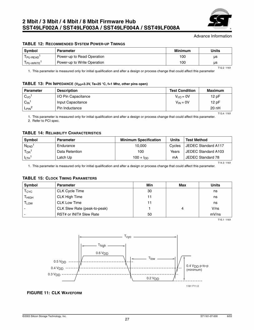
FIGURE 11: CLK WAVEFORM
TABLE 12: RECOMMENDED SYSTEM POWER-UP TIMINGS
Symbol Parameter Minimum Units
TPU-READ1 Power-up to Read Operation 100 µs
TPU-WRITE1 Power-up to Write Operation 100 µs
T12.2 11611. This parameter is measured only for initial qualification and after a design or process change that could affect this parameter
TABLE 13: PIN IMPEDANCE (VDD=3.3V, Ta=25 °C, f=1 Mhz, other pins open)
Parameter Description Test Condition Maximum
CI/O1
1. This parameter is measured only for initial qualification and after a design or process change that could affect this parameter.
I/O Pin Capacitance VI/O = 0V 12 pF
CIN1 Input Capacitance VIN = 0V 12 pF
LPIN2
2. Refer to PCI spec.
Pin Inductance 20 nHT13.4 1161
TABLE 14: RELIABILITY CHARACTERISTICS
Symbol Parameter Minimum Specification Units Test Method
NEND1
1. This parameter is measured only for initial qualification and after a design or process change that could affect this parameter.
Endurance 10,000 Cycles JEDEC Standard A117
TDR1 Data Retention 100 Years JEDEC Standard A103
ILTH1 Latch Up 100 + IDD mA JEDEC Standard 78
T14.3 1161
TABLE 15: CLOCK TIMING PARAMETERS
Symbol Parameter Min Max Units
TCYC CLK Cycle Time 30 ns
THIGH CLK High Time 11 ns
TLOW CLK Low Time 11 ns
- CLK Slew Rate (peak-to-peak) 1 4 V/ns
- RST# or INIT# Slew Rate 50 mV/nsT15.1 1161
1161 F11.0
0.4 VDD p-to-p(minimum)
Tcyc
Thigh
Tlow
0.4 VDD
0.3 VDD
0.6 VDD
0.2 VDD
0.5 VDD
28
Advance Information
2 Mbit / 3 Mbit / 4 Mbit / 8 Mbit Firmware HubSST49LF002A / SST49LF003A / SST49LF004A / SST49LF008A
©2003 Silicon Storage Technology, Inc. S71161-07-000 6/03
AC Characteristics (FWH Mode)
TABLE 16: READ/WRITE CYCLE TIMING PARAMETERS, VDD =3.0-3.6V (FWH MODE)
Symbol Parameter Min Max Units
TCYC Clock Cycle Time 30 ns
TSU Data Set Up Time to Clock Rising 7 ns
TDH Clock Rising to Data Hold Time 0 ns
TVAL1
1. Minimum and maximum times have different loads. See PCI spec.
Clock Rising to Data Valid 2 11 ns
TBP Byte Programming Time 20 µs
TSE Sector-Erase Time 25 ms
TBE Block-Erase Time 25 ms
TSCE Chip-Erase Time 100 ms
TON Clock Rising to Active (Float to Active Delay) 2 ns
TOFF Clock Rising to Inactive (Active to Float Delay) 28 nsT16.3 1161
TABLE 17: AC INPUT/OUTPUT SPECIFICATIONS, VDD =3.0-3.6V (FWH MODE)
Symbol Parameter
Limits
Test ConditionsMin Max Units
IOH(AC) Switching Current High -12 VDD
-17.1(VDD-VOUT)Equation C1
1. See PCI spec.
mAmA
0 < VOUT ≤ 0.3VDD
0.3VDD < VOUT < 0.9VDD
0.7VDD < VOUT <VDD
(Test Point) -32 VDD mA VOUT=0.7VDD
IOL(AC) Switching Current Low 16 VDD
26.7 VOUT
Equation D1 mAmA
VDD >VOUT ≥0.6VDD
0.6VDD > VOUT > 0.1VDD
0.18VDD > VOUT > 0
(Test Point) 38 VDD mA VOUT=0.18VDD
ICL Low Clamp Current -25+(VIN+1)/0.015 mA -3 < VIN ≤ -1ICH High Clamp Current 25+(VIN-VDD-1)/0.015 mA VDD+4 > VIN ≤ VDD+1
slewr2
2. PCI specification output load is used.
Output Rise Slew Rate 1 4 V/ns 0.2VDD-0.6VDD load
slewf2 Output Fall Slew Rate 1 4 V/ns 0.6VDD-0.2VDD loadT17.3 1161
TABLE 18: RESET TIMING PARAMETERS, VDD =3.0-3.6V (FWH MODE)
Symbol Parameter Min Max Units
TPRST VDD stable to Reset Low 1 ms
TKRST Clock Stable to Reset Low 100 µs
TRSTP RST# Pulse Width 100 ns
TRSTF RST# Low to Output Float 48 ns
TRST1
1. There will be a latency of TRSTE if a reset procedure is performed during a Program or Erase operation.
RST# High to FWH4 Low 1 µs
TRSTE RST# Low to reset during Sector-/Block-Erase or Program 10 µsT18.5 1161
Advance Information
2 Mbit / 3 Mbit / 4 Mbit / 8 Mbit Firmware HubSST49LF002A / SST49LF003A / SST49LF004A / SST49LF008A
29©2003 Silicon Storage Technology, Inc. S71161-07-000 6/03
FIGURE 12: RESET TIMING DIAGRAM
FIGURE 13: OUTPUT TIMING PARAMETERS
CLK
VDD
RST#/INIT#
FWH4
FWH[3:0]
1161 F12.0
TPRST
TKRST
TRSTP
TRSTF
TRSTESector-/Block-Erase
or Program operation aborted
TRST
TVAL
VTEST
VTL
VTH
TOFF
TON
1161 F13.0
CLK
FWH [3:0](Valid Output Data)
FWH [3:0](Float Output Data)

30
Advance Information
2 Mbit / 3 Mbit / 4 Mbit / 8 Mbit Firmware HubSST49LF002A / SST49LF003A / SST49LF004A / SST49LF008A
©2003 Silicon Storage Technology, Inc. S71161-07-000 6/03
FIGURE 14: INPUT TIMING PARAMETERS
TABLE 19: INTERFACE MEASUREMENT CONDITION PARAMETERS
Symbol Value Units
VTH1
1. The input test environment is done with 0.1 VDD of overdrive over VIH and VIL. Timing parameters must be met with no more overdrive than this. VMAX specified the maximum peak-to-peak waveform allowed for measuring input timing. Production testing may use different voltage values, but must correlate results back to these parameters.
0.6 VDD V
VTL1 0.2 VDD V
VTEST 0.4 VDD V
VMAX1 0.4 VDD V
Input Signal Edge Rate 1 V/nsT19.3 1161
TSU
TDH
InputsValid
1161 F14.0
CLK
FWH [3:0](Valid Input Data)
VTEST
VTL
VMAX
VTH
Advance Information
2 Mbit / 3 Mbit / 4 Mbit / 8 Mbit Firmware HubSST49LF002A / SST49LF003A / SST49LF004A / SST49LF008A
31©2003 Silicon Storage Technology, Inc. S71161-07-000 6/03
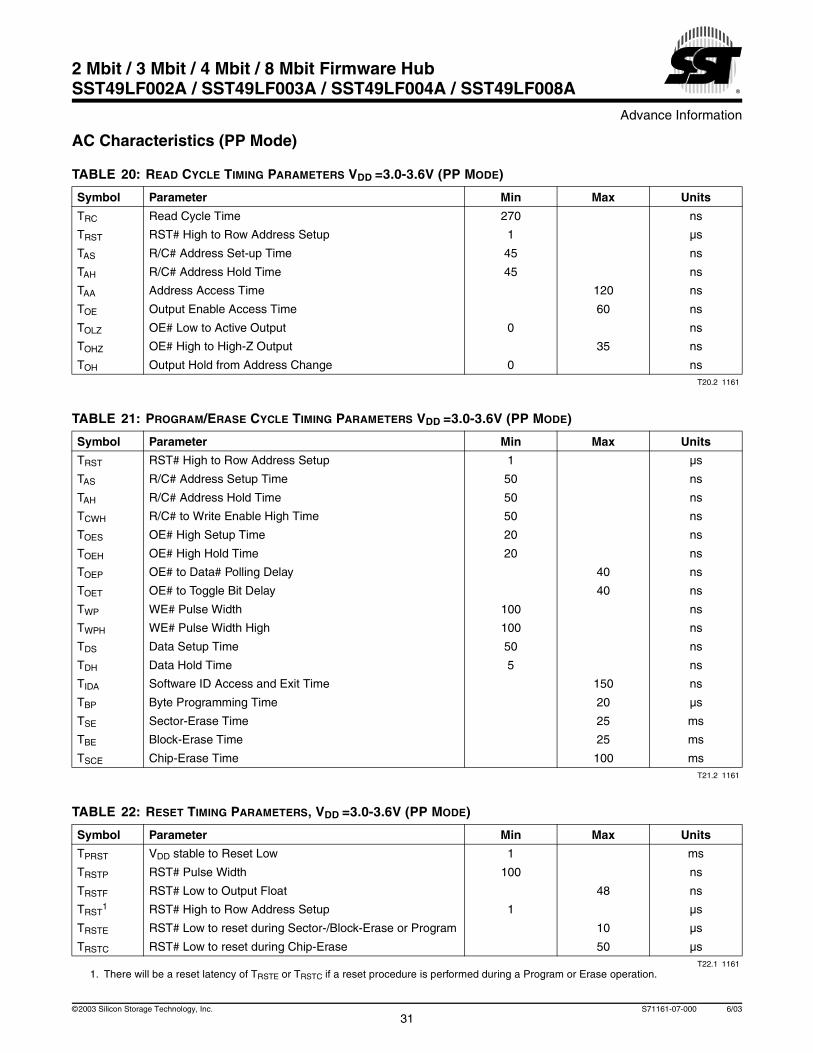
AC Characteristics (PP Mode)
TABLE 20: READ CYCLE TIMING PARAMETERS VDD =3.0-3.6V (PP MODE)
Symbol Parameter Min Max Units
TRC Read Cycle Time 270 ns
TRST RST# High to Row Address Setup 1 µs
TAS R/C# Address Set-up Time 45 ns
TAH R/C# Address Hold Time 45 ns
TAA Address Access Time 120 ns
TOE Output Enable Access Time 60 ns
TOLZ OE# Low to Active Output 0 ns
TOHZ OE# High to High-Z Output 35 ns
TOH Output Hold from Address Change 0 nsT20.2 1161
TABLE 21: PROGRAM/ERASE CYCLE TIMING PARAMETERS VDD =3.0-3.6V (PP MODE)
Symbol Parameter Min Max Units
TRST RST# High to Row Address Setup 1 µs
TAS R/C# Address Setup Time 50 ns
TAH R/C# Address Hold Time 50 ns
TCWH R/C# to Write Enable High Time 50 ns
TOES OE# High Setup Time 20 ns
TOEH OE# High Hold Time 20 ns
TOEP OE# to Data# Polling Delay 40 ns
TOET OE# to Toggle Bit Delay 40 ns
TWP WE# Pulse Width 100 ns
TWPH WE# Pulse Width High 100 ns
TDS Data Setup Time 50 ns
TDH Data Hold Time 5 ns
TIDA Software ID Access and Exit Time 150 ns
TBP Byte Programming Time 20 µs
TSE Sector-Erase Time 25 ms
TBE Block-Erase Time 25 ms
TSCE Chip-Erase Time 100 msT21.2 1161
TABLE 22: RESET TIMING PARAMETERS, VDD =3.0-3.6V (PP MODE)
Symbol Parameter Min Max Units
TPRST VDD stable to Reset Low 1 ms
TRSTP RST# Pulse Width 100 ns
TRSTF RST# Low to Output Float 48 ns
TRST1
1. There will be a reset latency of TRSTE or TRSTC if a reset procedure is performed during a Program or Erase operation.
RST# High to Row Address Setup 1 µs
TRSTE RST# Low to reset during Sector-/Block-Erase or Program 10 µs
TRSTC RST# Low to reset during Chip-Erase 50 µsT22.1 1161
32
Advance Information
2 Mbit / 3 Mbit / 4 Mbit / 8 Mbit Firmware HubSST49LF002A / SST49LF003A / SST49LF004A / SST49LF008A
©2003 Silicon Storage Technology, Inc. S71161-07-000 6/03
FIGURE 15: RESET TIMING DIAGRAM (PP MODE)
FIGURE 16: READ CYCLE TIMING DIAGRAM (PP MODE)
VDD
RST#
Addresses
R/C#
DQ7-0
1161 F15.0
TPRST
TRSTP
TRSTF
TRSTE
Row Address
Sector-/Block-Erase or Program operation
aborted
TRST
TRSTC Chip-Eraseaborted
1161 F16.0
Column Address
Data ValidHigh-Z
Row AddressColumn AddressRow Address
RST#
Addresses
R/C#
VIH
High-Z
TRST TRC
TAS TAH TAH
TAA
TOETOLZ
TOHZ
TOH
TAS
WE#
OE#
DQ7-0
TRSTP
Advance Information
2 Mbit / 3 Mbit / 4 Mbit / 8 Mbit Firmware HubSST49LF002A / SST49LF003A / SST49LF004A / SST49LF008A
33©2003 Silicon Storage Technology, Inc. S71161-07-000 6/03
FIGURE 17: WRITE CYCLE TIMING DIAGRAM (PP MODE)
FIGURE 18: DATA# POLLING TIMING DIAGRAM (PP MODE)
1161 F17.0
Column AddressRow Address
Data Valid
RST#
Addresses
R/C#
TRST
TAS TAH
TCWH
TWP TWPH
TOEH
TDHTDS
TAHTAS
WE#
OE#
DQ7-0
TOES
TRSTP
1161 F18.0
Addresses
R/C#
TOEP
Row Column
WE#
OE#
DQ7 D#D D# D
34
Advance Information
2 Mbit / 3 Mbit / 4 Mbit / 8 Mbit Firmware HubSST49LF002A / SST49LF003A / SST49LF004A / SST49LF008A
©2003 Silicon Storage Technology, Inc. S71161-07-000 6/03
FIGURE 19: TOGGLE BIT TIMING DIAGRAM (PP MODE)
FIGURE 20: BYTE-PROGRAM TIMING DIAGRAM (PP MODE)
1161 F19.0
Addresses
R/C#
TOET
Row Column
WE#
OE#
DQ6 D D
1161 F20.0
TWP
TWPH
TBP
Four-Byte Code for Byte-Program
5555 2AAA 5555 BA
SB0
BA = Byte-Program Address
SB1 SB2 SB3 Internal Program Starts
WE#
Addresses
R/C#
OE#
Data55AA A0DQ7-0
Advance Information
2 Mbit / 3 Mbit / 4 Mbit / 8 Mbit Firmware HubSST49LF002A / SST49LF003A / SST49LF004A / SST49LF008A
35©2003 Silicon Storage Technology, Inc. S71161-07-000 6/03
FIGURE 21: SECTOR-ERASE TIMING DIAGRAM (PP MODE)
FIGURE 22: BLOCK-ERASE TIMING DIAGRAM (PP MODE)
1161 F21.0
TWP
TWPH
TSE
Six-Byte code forSector-Erase Operation
5555 2AAA 5555 5555 2AAA SAx
SB0
SAx = Sector Address
SB1 SB2 SB3 SB4 SB5 Internal Erasure Starts
WE#
Addresses
R/C#
OE#
55AA55AA 80 30DQ7-0
1161 F22.0
TWP
TWPH
TBE
Six-Byte code forBlock-Erase Operation
5555 2AAA 5555 5555 2AAA BAx
SB0
BAx = Block Address
SB1 SB2 SB3 SB4 SB5 Internal Erasure Starts
WE#
Addresses
R/C#
OE#
55AA55AA 80 50DQ7-0
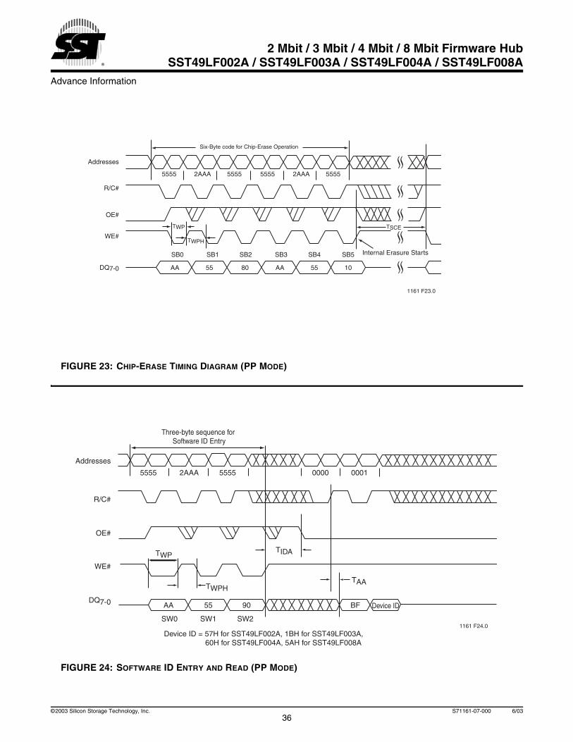
36
Advance Information
2 Mbit / 3 Mbit / 4 Mbit / 8 Mbit Firmware HubSST49LF002A / SST49LF003A / SST49LF004A / SST49LF008A
©2003 Silicon Storage Technology, Inc. S71161-07-000 6/03
FIGURE 23: CHIP-ERASE TIMING DIAGRAM (PP MODE)
FIGURE 24: SOFTWARE ID ENTRY AND READ (PP MODE)
1161 F23.0
TWP
TWPH
TSCE
Six-Byte code for Chip-Erase Operation
5555 2AAA 5555 5555 2AAA 5555
SB0 SB1 SB2 SB3 SB4 SB5 Internal Erasure Starts
WE#
Addresses
R/C#
OE#
55AA55AA 80 10DQ7-0
1161 F24.0
Addresses
TIDA
DQ7-0
WE#
SW0
Device ID = 57H for SST49LF002A, 1BH for SST49LF003A, 60H for SST49LF004A, 5AH for SST49LF008A
SW1 SW2
5555 2AAA 5555 0000 0001
OE#
R/C#
Three-byte sequence for Software ID Entry
TWP
TWPHTAA
BF Device ID55AA 90
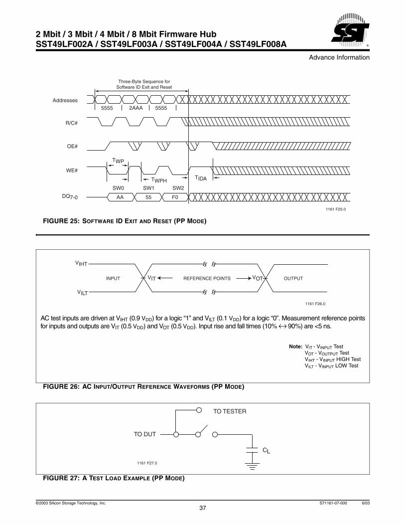
Advance Information
2 Mbit / 3 Mbit / 4 Mbit / 8 Mbit Firmware HubSST49LF002A / SST49LF003A / SST49LF004A / SST49LF008A
37©2003 Silicon Storage Technology, Inc. S71161-07-000 6/03
FIGURE 25: SOFTWARE ID EXIT AND RESET (PP MODE)
FIGURE 26: AC INPUT/OUTPUT REFERENCE WAVEFORMS (PP MODE)
FIGURE 27: A TEST LOAD EXAMPLE (PP MODE)
1161 F25.0
Addresses
DQ7-0
TIDA
TWP
TWPH
WE#
SW0 SW1 SW2
5555 2AAA 5555
Three-Byte Sequence forSoftware ID Exit and Reset
OE#
R/C#
AA 55 F0
1161 F26.0
REFERENCE POINTS OUTPUTINPUT VIT
VIHT
VILT
VOT
AC test inputs are driven at VIHT (0.9 VDD) for a logic “1” and VILT (0.1 VDD) for a logic “0”. Measurement reference pointsfor inputs and outputs are VIT (0.5 VDD) and VOT (0.5 VDD). Input rise and fall times (10% ↔ 90%) are <5 ns.
Note: VIT - VINPUT TestVOT - VOUTPUT TestVIHT - VINPUT HIGH TestVILT - VINPUT LOW Test
1161 F27.0
TO TESTER
TO DUT
CL
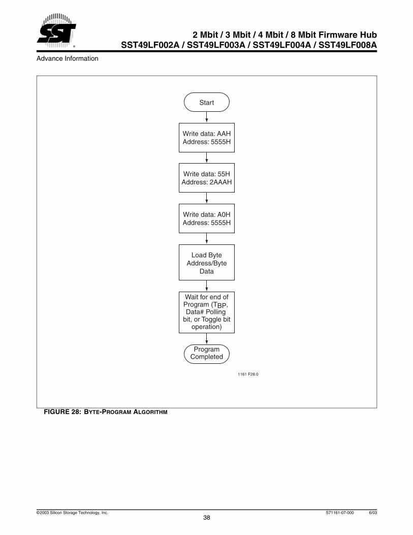
38
Advance Information
2 Mbit / 3 Mbit / 4 Mbit / 8 Mbit Firmware HubSST49LF002A / SST49LF003A / SST49LF004A / SST49LF008A
©2003 Silicon Storage Technology, Inc. S71161-07-000 6/03
FIGURE 28: BYTE-PROGRAM ALGORITHM
1161 F28.0
Start
Write data: AAHAddress: 5555H
Write data: 55HAddress: 2AAAH
Write data: A0HAddress: 5555H
Load ByteAddress/Byte
Data
Wait for end ofProgram (TBP, Data# Polling
bit, or Toggle bitoperation)
ProgramCompleted
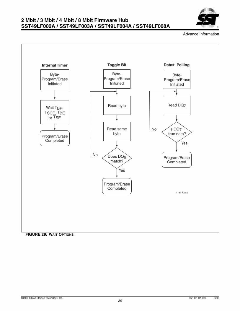
Advance Information
2 Mbit / 3 Mbit / 4 Mbit / 8 Mbit Firmware HubSST49LF002A / SST49LF003A / SST49LF004A / SST49LF008A
39©2003 Silicon Storage Technology, Inc. S71161-07-000 6/03
FIGURE 29: WAIT OPTIONS
1161 F29.0
Wait TBP,TSCE, TBE
or TSE
Byte- Program/Erase
Initiated
Internal Timer Toggle Bit
Yes
Yes
No
No
Program/EraseCompleted
Does DQ6match?
Read samebyte
Data# Polling
Program/EraseCompleted
Program/EraseCompleted
Read byte
Is DQ7 =true data?
Read DQ7
Byte-Program/Erase
Initiated
Byte-Program/Erase
Initiated

40
Advance Information
2 Mbit / 3 Mbit / 4 Mbit / 8 Mbit Firmware HubSST49LF002A / SST49LF003A / SST49LF004A / SST49LF008A
©2003 Silicon Storage Technology, Inc. S71161-07-000 6/03
FIGURE 30: SOFTWARE PRODUCT COMMAND FLOWCHARTS
1161 F30.0
Write data: AAHAddress: 5555H
Software Product ID EntryCommand Sequence
Write data: 55HAddress: 2AAAH
Write data: 90HAddress: 5555H
Wait TIDA
Read Software ID
Write data: AAHAddress: 5555H
Software Product ID Exit &Reset Command Sequence
Write data: 55HAddress: 2AAAH
Write data: F0HAddress: 5555H
Write data: F0HAddress: XXH
Return to normaloperation
Wait TIDA
Wait TIDA
Return to normaloperation
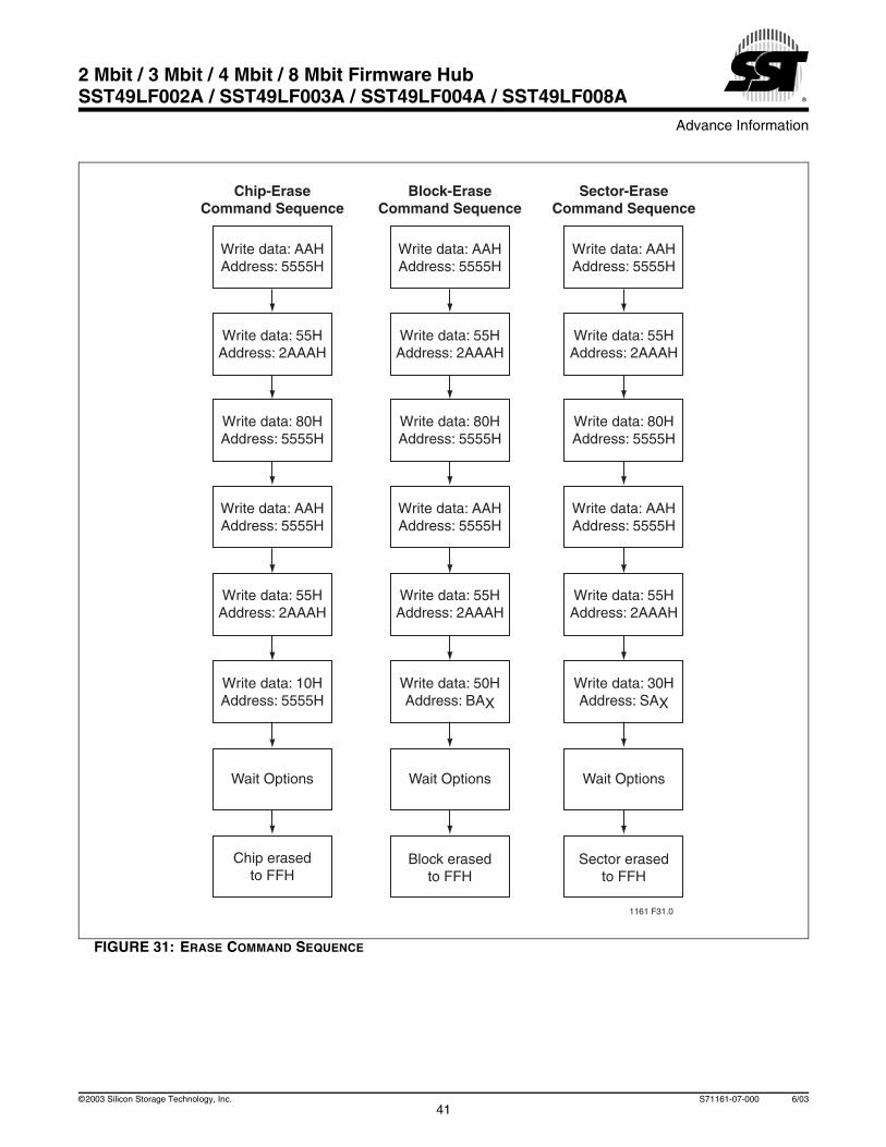
Advance Information
2 Mbit / 3 Mbit / 4 Mbit / 8 Mbit Firmware HubSST49LF002A / SST49LF003A / SST49LF004A / SST49LF008A
41©2003 Silicon Storage Technology, Inc. S71161-07-000 6/03
FIGURE 31: ERASE COMMAND SEQUENCE
1161 F31.0
Write data: AAHAddress: 5555H
Chip-EraseCommand Sequence
Write data: 55HAddress: 2AAAH
Write data: 80HAddress: 5555H
Write data: 55HAddress: 2AAAH
Write data: 10HAddress: 5555H
Write data: AAHAddress: 5555H
Wait Options
Chip erasedto FFH
Write data: AAHAddress: 5555H
Sector-EraseCommand Sequence
Write data: 55HAddress: 2AAAH
Write data: 80HAddress: 5555H
Write data: 55HAddress: 2AAAH
Write data: 30HAddress: SAX
Write data: AAHAddress: 5555H
Wait Options
Sector erasedto FFH
Write data: AAHAddress: 5555H
Block-EraseCommand Sequence
Write data: 55HAddress: 2AAAH
Write data: 80HAddress: 5555H
Write data: 55HAddress: 2AAAH
Write data: 50HAddress: BAX
Write data: AAHAddress: 5555H
Wait Options
Block erasedto FFH
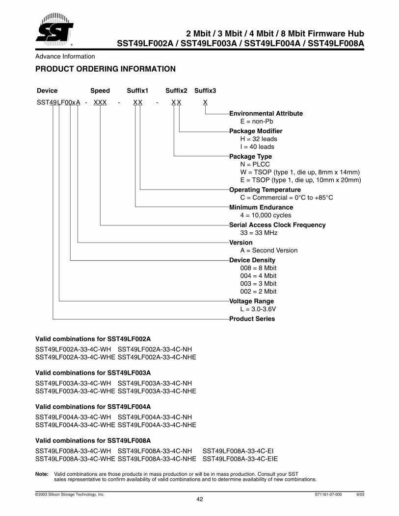
42
Advance Information
2 Mbit / 3 Mbit / 4 Mbit / 8 Mbit Firmware HubSST49LF002A / SST49LF003A / SST49LF004A / SST49LF008A
©2003 Silicon Storage Technology, Inc. S71161-07-000 6/03
PRODUCT ORDERING INFORMATION
Valid combinations for SST49LF002A
SST49LF002A-33-4C-WH SST49LF002A-33-4C-NHSST49LF002A-33-4C-WHE SST49LF002A-33-4C-NHE
Valid combinations for SST49LF003A
SST49LF003A-33-4C-WH SST49LF003A-33-4C-NHSST49LF003A-33-4C-WHE SST49LF003A-33-4C-NHE
Valid combinations for SST49LF004A
SST49LF004A-33-4C-WH SST49LF004A-33-4C-NHSST49LF004A-33-4C-WHE SST49LF004A-33-4C-NHE
Valid combinations for SST49LF008A
SST49LF008A-33-4C-WH SST49LF008A-33-4C-NH SST49LF008A-33-4C-EISST49LF008A-33-4C-WHE SST49LF008A-33-4C-NHE SST49LF008A-33-4C-EIE
Note: Valid combinations are those products in mass production or will be in mass production. Consult your SST sales representative to confirm availability of valid combinations and to determine availability of new combinations.
Device Speed Suffix1 Suffix2 Suffix3
SST49LF00xA - XXX - XX - X X X
Environmental AttributeE = non-Pb
Package ModifierH = 32 leadsI = 40 leads
Package TypeN = PLCCW = TSOP (type 1, die up, 8mm x 14mm)E = TSOP (type 1, die up, 10mm x 20mm)
Operating TemperatureC = Commercial = 0°C to +85°C
Minimum Endurance4 = 10,000 cycles
Serial Access Clock Frequency33 = 33 MHz
VersionA = Second Version
Device Density008 = 8 Mbit004 = 4 Mbit003 = 3 Mbit002 = 2 Mbit
Voltage RangeL = 3.0-3.6V
Product Series

Advance Information
2 Mbit / 3 Mbit / 4 Mbit / 8 Mbit Firmware HubSST49LF002A / SST49LF003A / SST49LF004A / SST49LF008A
43©2003 Silicon Storage Technology, Inc. S71161-07-000 6/03
PACKAGING DIAGRAMS
32-LEAD PLASTIC LEAD CHIP CARRIER (PLCC) SST PACKAGE CODE: NH
.040
.030
.021
.013.530.490
.095
.075
.140
.125
.032
.026
.032
.026
.029
.023
.453
.447
.553
.547.595.585
.495
.485 .112.106
.042
.048
.048
.042
.015 Min.
TOP VIEW SIDE VIEW BOTTOM VIEW
12 32
.400BSC
32-plcc-NH-3
Note: 1. Complies with JEDEC publication 95 MS-016 AE dimensions, although some dimensions may be more stringent.2. All linear dimensions are in inches (max/min).3. Dimensions do not include mold flash. Maximum allowable mold flash is .008 inches.4. Coplanarity: 4 mils.
.050BSC
.050BSC
OptionalPin #1
Identifier .020 R.MAX.
R.x 30˚
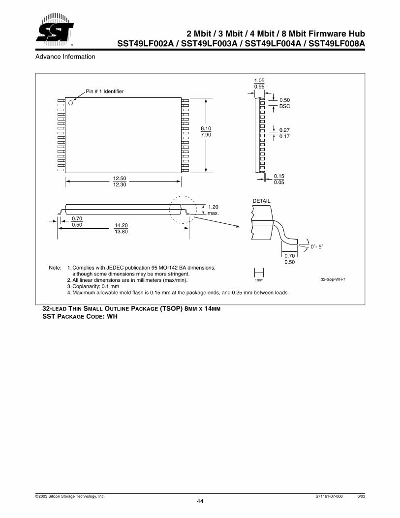
44
Advance Information
2 Mbit / 3 Mbit / 4 Mbit / 8 Mbit Firmware HubSST49LF002A / SST49LF003A / SST49LF004A / SST49LF008A
©2003 Silicon Storage Technology, Inc. S71161-07-000 6/03
32-LEAD THIN SMALL OUTLINE PACKAGE (TSOP) 8MM X 14MM
SST PACKAGE CODE: WH
32-tsop-WH-7
Note: 1. Complies with JEDEC publication 95 MO-142 BA dimensions,although some dimensions may be more stringent.
2. All linear dimensions are in millimeters (max/min).3. Coplanarity: 0.1 mm4. Maximum allowable mold flash is 0.15 mm at the package ends, and 0.25 mm between leads.
1.20max.
1mm
Pin # 1 Identifier
12.5012.30
14.2013.80
0.700.50
8.107.90
0.270.17
0.50BSC
1.050.95
0.150.05
0.700.50
0˚- 5˚
DETAIL

Advance Information
2 Mbit / 3 Mbit / 4 Mbit / 8 Mbit Firmware HubSST49LF002A / SST49LF003A / SST49LF004A / SST49LF008A
45©2003 Silicon Storage Technology, Inc. S71161-07-000 6/03
40-LEAD THIN SMALL OUTLINE PACKAGE (TSOP) 10MM X 20MM (FOR SST49LF008A ONLY)SST PACKAGE CODE: EI
TABLE 23: REVISION HISTORY
Revision Draft Changes Date
06 • 2002 Data Book• Changed Transient Voltage from -1.0V to VDD +1.0V to -2.0V to VDD +2.0V to
match Intel FWH spec per IBM requirement.• Added footnote for Transient Voltage.• Updated footnote for Output Short Circuit Current.• Updated Data# Polling description• Corrected the values in Table 5 on page 19: General Purpose Inputs Register• Added note to Table 11 on page 26: DC Operating Characteristics
July 2001
07 • Added 40-lead TSOP for SST49LF008A only• Corrected the IDD Test Conditions in Table 11 on page 26
June 2003
18.5018.30
20.2019.80
0.700.50
10.109.90
0.270.17
1.050.95
0.150.05
0.700.50
40-tsop-EI-7
Note: 1. Complies with JEDEC publication 95 MO-142 CD dimensions,although some dimensions may be more stringent.
2. All linear dimensions are in millimeters (max/min).3. Coplanarity: 0.1 mm4. Maximum allowable mold flash is 0.15 mm at the package ends, and 0.25 mm between leads.
Pin # 1 Identifier
0.50BSC
1.20max.
0˚- 5˚
DETAIL
1mm
Silicon Storage Technology, Inc. • 1171 Sonora Court • Sunnyvale, CA 94086 • Telephone 408-735-9110 • Fax 408-735-9036www.SuperFlash.com or www.sst.com