5 current mode control modeling
TRANSCRIPT

CurCurrrent-mode contrent-mode control is the industrol is the industry standary standardd
method of contrmethod of controlling solling switcwitching pohing powwer super sup--
plies. plies. A contrA control rol refefererence is used to rence is used to reegulagulatete
the peak curthe peak currrent of the conent of the convvererter dirter directlectlyy,,
simplifying the dsimplifying the dynamics of the conynamics of the convvererterter. In. In
ffact,act, ffor most poor most powwer suppler supply design engy design engineerineers,s,
a simple single-pole model of a cura simple single-pole model of a currrent sourent sourcece
ffeeding a caeeding a capacitor sufpacitor sufff ices fices for mor mucuch of theirh of their
design wdesign worork. k. And most of the timeAnd most of the time,, this modelthis model
wwororks fks f ineine. Ho. Howweevverer,, in some ain some applicapplications,tions, thethe
curcurrrent fent feedbaceedback loop becomes unstak loop becomes unstabble underle under
cercertain opertain operaating conditions,ting conditions, and the simpleand the simple
single-pole model cannot prsingle-pole model cannot predict this eedict this evvent.ent.
1©Copyright 2006 Switching Power Magazine

In this article, we’ll show a very simple extension to the existing single-pole model that accountsfor the subharmonic oscillation phenomenon seen in current-mode controlled converters.Without needing any complex analysis, the oscillation phenomenon, ramp addition, and controltransfer function are unified in a single model that works for voltage-mode, current-mode, andconditions in between when the current gain is low.
When current-mode control was first introduced to the power electronics community in the early1980s, it was immediately seized upon as a superior control scheme. This simple control scheme, how-ever, had an inherent oscillation phenomenon that took many years to properly model. Simple modelsexcluded the oscillation phenomenon. More complex approaches focused on discrete time and sam-pled-data methods, due to the high-frequency sampling nature of the current-mode controller. Whilemuch of this work was very good and accurate, it never found its way into mainstream design becausethe results were too complex.
What we need as designers is a model that combines the best of both approaches— a very simple andintuitive model, enhanced with the critical features from sampled-data modeling that are easy to apply.This will allow you to:
1. Model and predict control transfer functions with greater accuracy;2. Select the proper compensation ramp;3. Use a single small-signal model for both the control transfer functions and current loop
stabilization; and4. Decide when you need to add a ramp to your power circuit, and how much to add.
2©Copyright 2006 Switching Power Magazine

Design Workshop
Power Supply
Gain a lifetime of design experience
. . . in four days.
FFoorr ddaatteess aanndd rreesseerrvvaattiioonnss,, vviissiitt wwwwww..rriiddlleeyyeennggiinneeeerriinngg..ccoomm
Morning Theory ● Converter Topologies● Inductor Design● Transformer Design● Leakage Inductance● Design with Power 4-5-6
Afternoon Lab ● Design and Build
Flyback Transformer● Design and Build
Forward Transformer● Design and Build
Forward Inductor● Magnetics Characterization● Snubber Design● Flyback and Forward
Circuit Testing
Day 1 Day 2
Morning Theory
● Small Signal Analysis of Power Stages
● CCM and DCM Operation● Converter Characteristics● Voltage-Mode Control● Closed-Loop Design
with Power 4-5-6
Afternoon Lab
● Measuring Power Stage Transfer Functions
● Compensation Design● Loop Gain Measurement● Closed Loop Performance
Workshop Agenda
Morning Theory
● Current-Mode Control● Circuit Implementation● Modeling of Current Mode● Problems with Current Mode● Closed-Loop Design for
Current Mode w/Power 4-5-6
Afternoon Lab
● Closing the Current Loop● New Power Stage
Transfer Functions● Closing the Voltage
Compensation Loop● Loop Gain Design
and Measurement
Morning Theory
● Multiple Output Converters● Magnetics Proximity Loss● Magnetics Winding Layout● Second Stage Filter Design
Afternoon Lab
● Design and Build Multiple Output Flyback Transformers
● Testing of Cross Regulation for Different Transformers
● Second Stage Filter Design and Measurement
● Loop Gain with Multiple Outputs and Second Stage Filters
Day 3 Day 4
Only 24 reservations are accepted. $2495 tuition includes POWER 4-5-6 Full Version, lab manuals,breakfast and lunch daily. Payment is due 30 days prior to workshop to maintain reservation.
Ridley Engineeringwww.ridleyengineering.com
770 640 9024885 Woodstock Rd.
Suite 430-382Roswell, GA 30075 USA
The analytical results presented here are the result ofcomplex modeling techniques using sampled-data.Once armed with these equations, understanding anddesigning a current loop becomes very simple. Youdon’t need to be familiar with any of the morecomplex analysis techniques to obtain the bene-fits of the extended model.
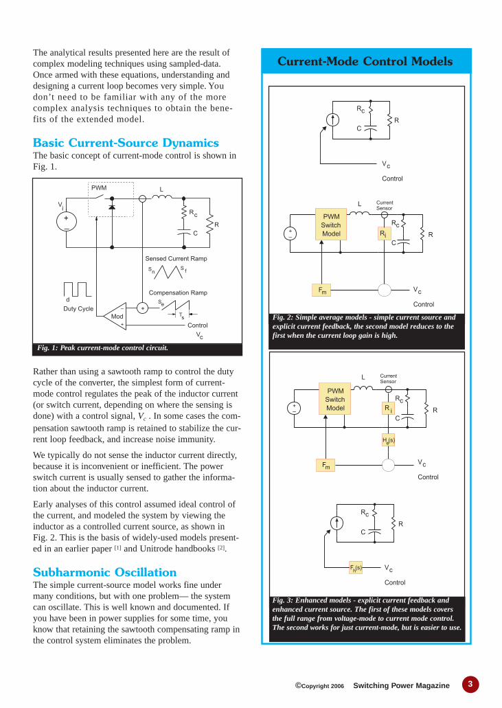
Basic Current-Source DynamicsThe basic concept of current-mode control is shown inFig. 1.
Rather than using a sawtooth ramp to control the dutycycle of the converter, the simplest form of current-mode control regulates the peak of the inductor current(or switch current, depending on where the sensing isdone) with a control signal, Vc . In some cases the com-pensation sawtooth ramp is retained to stabilize the cur-rent loop feedback, and increase noise immunity.
We typically do not sense the inductor current directly,because it is inconvenient or inefficient. The powerswitch current is usually sensed to gather the informa-tion about the inductor current.
Early analyses of this control assumed ideal control ofthe current, and modeled the system by viewing theinductor as a controlled current source, as shown inFig. 2. This is the basis of widely-used models present-ed in an earlier paper [1] and Unitrode handbooks [2].
Subharmonic OscillationThe simple current-source model works fine undermany conditions, but with one problem— the systemcan oscillate. This is well known and documented. Ifyou have been in power supplies for some time, youknow that retaining the sawtooth compensating ramp inthe control system eliminates the problem.
Fig. 3: Enhanced models - explicit current feedback andenhanced current source. The first of these models coversthe full range from voltage-mode to current mode control.The second works for just current-mode, but is easier to use.
Fig. 1: Peak current-mode control circuit.
Current-Mode Control Models
Fig. 2: Simple average models - simple current source andexplicit current feedback, the second model reduces to thefirst when the current loop gain is high.
DESIGNER’S SERIES
3©Copyright 2006 Switching Power Magazine

Most small-signal models don’t explain, however, whatthis does to the control characteristics. The more com-plex model of Fig. 2 with an explicit current feedback loop-still does not show the tendency in the system to oscillate.
Fig. 4 shows the nature of the current loop oscillation.At duty cycles approaching 50% and beyond, the peakcurrent is regulated at a fixed value, but the current willoscillate back and forth on subsequent switching cycles.
The situation is really very simple, as pointed out in anearly paper [3]. Current-mode oscillation is like anyother oscillation— if it is undamped, it will continue toring and grow in amplitude under some conditions. If itis damped, the oscillations decrease and die out.
While it is easy to draw oscillating waveforms and seewhat is happening that causes instability, sampled-datamodeling is necessary to obtain analytical results. Thesampled-data or discrete-time analysis of this phenome-non, required because of its high frequency, has beenwith us for some time. So why don’t most engineersuse this in their work? Because the analysis is usuallytoo complex. It has been shown [4] that very practicalresults can be simplified into a user-friendly form.
Sampled-Data AnalysisEarly modeling combined simple average analysis withseparate explanations detailing how the current signalcould become unstable. The small-signal model andphysical explanation for instability were later recon-ciled [4]. This paper expanded upon earlier work [5], butfound a way to simplify the results into a more useful format.
Other analyses have subsequently analyzed the sameissue. Many of these agree in the method of tacklingthe problem and provide supporting experimental data.Others disagree in the methods but still come to the sameconclusions about the second-order oscillatory systemthat results. They are all consistent in the values derived.
The good news is that we no longer need to be stymiedwith conflicting sampled-data modeling techniques, ordebates about how to analyze a system. Instead, we canuse the common design equations everyone agreesupon, and move products out the door.
Dominant Pole ModelsThe equivalent control system diagram for current-mode control is shown in Fig. 2. The inductor currentfeedback becomes an inner feedback loop. We are usu-ally concerned with the transfer function from the con-trol input shown to the output of the power converter.The input is typically the input to the duty cycle modu-lator, provided by the error amplifier output.
Most designers are familiar with the fact that the cur-rent feedback loop reduces the main dynamic of thesystem to a dominant single-pole type response. This isa result of viewing the inductor as a controlled currentsource rather than as a state of the system, as indicatedin the simple model of Figure 2.
The results of existing analyses for the three main typesof converter are summarized below.
Buck ConverterThe low-frequency model of the buck converter, com-monly used by designers, and summarized in [2] isgiven by:
The load resistor and capacitor determine the dominantpole, as we would expect for a current source feedingan RC network.
In [4], there is a more accurate expression for the domi-nant pole of the buck, involving the external ramp slopeand operating point of the converter:
This refinement is usually unnecessary. It only becomesimportant when an excessively steep ramp is used,showing how the pole can move. In most cases, thesimplified form of the dominant pole is adequate fordesign purposes.
The power stage transfer function zero is determined bythe equivalent series resistance of the capacitor:
This expression for the output capacitor zero is thesame for all the converters.
Fig. 4: Subharmonic oscillation waveforms.
DESIGNER’S SERIES
4©Copyright 2006 Switching Power Magazine

Boost ConverterThe boost converter has an additional term in the con-trol transfer function, caused by the right-half-plane(rhp) zero (covered in our January 2001 issue) :
The dominant pole is located at
and the rhp zero is at
Note that the rhp zero expression is exactly the same asthat for voltage-mode control. Using current mode doesnot move this at all, although it is easier to compensate,as we do not need to deal with the additional doublepole response of the LC filter that is present with volt-age-mode control.
Flyback ConverterThe flyback converter also has an rhp zero term in thecontrol transfer function:
with the dominant pole determined by
and the rhp zero at:
As with the boost converter, this zero location is thesame as for voltage-mode control.
Measured High-Frequency EffectsTo account for the observed oscillation in the current-mode system, we need to add a high-frequency correc-tion term to the basic power stage transfer functions.The converter transfer functions are modified from theabove section by
Without even considering the sampled-data type analy-sis, we can see what the form of the transfer functionmust be through laboratory experiments. One way itbecomes clear is to measure the control-to-output trans-fer functions, while adding different amounts of com-pensating ramp to the system.
Fig. 5 shows measurements of power stage transferfunctions plotted beyond half the switching frequency.The characteristic at half the switching frequency is aclassic double pole response that can be seen in anyfundamental text on bode plots and control theory.
These curves are for a buck converter operating at a45% duty cycle. In the upper curve, there is no com-pensating ramp added, and there is a sharp peak in thetransfer function at half the switching frequency.
The curves below this have increasing amounts of com-pensating ramp added to them, until the bottom curve isreached and the double poles are overdamped.
Mathematical theoreticians may argue that measuringand predicting transfer functions up to this frequency isof questionable analytical merit. Yet, there is such adirect correlation between the peaking in the measure-ments and the oscillatory behavior of the system, that thecorrection term is vital for good and practical modeling.
When the system transfer function peaks with a high Q,the inductor current oscillates back and forth, as shownin Fig. 6. When the transfer function is well damped,the inductor current behaves, returning quickly to equi-librium after an initial disturbance.
Fig. 5: Power stage transfer functions plotted up to the switchingfrequency. Notice the obvious double-pole characteristic cen-tered at half the switching frequency.
DESIGNER’S SERIES
5©Copyright 2006 Switching Power Magazine

Pricing & Services
Analyzer & Accessories:Analog source/receiver unit AP200 USB* $12,500includes Digital Signal Processing (DSP) unit, Interface cables, and softwareOverseas Orders $13,100Differential Isolation Probes $650/pair5 Hz to 15 MHz Injection Isolator $595Power 4-5-6 $995**discounted price available only when purchasing the AP200
Services:Rental Units $1600/monthConsulting $250/hr + travel expense for On-Site
$200/hr Off-Site
* Free USB upgrade kit for AP200 Parallel users. Contact us for more information.
CCoonnttrrooll LLooooppss● Avoid expensive product Instability● Control loops change with line, load, and temperature● Optimize control loops to reduce cost and size
CCaappaacciittoorrss● Measure essential data not provided by manufacturers● Select optimum cost, size, shape, and performance
FFiilltteerrss● Characterize power systems filter building blocks ● Optimize performance at line and control frequencies● 15 MHz range shows filter effectiveness for EMI performance
MMaaggnneettiiccss● Design and specify more reliable magnetics● Measure critical parasitic components● Detect winding and material changes● Characterize component resonances up to 15 MHz
PPoowweerr LLiinnee HHaarrmmoonniiccss● Check IEC compliance for AC input systems● Measure line harmonics to 10 kHz● Avoid expensive redesign, and minimize test facility time
FrequencyRange
SelectivityBandwidth
OutputInjectionIsolator
Input Isolation
AveragingMethod
PC DataTransfer
0.01 Hz to15 MHz
1 Hz to 1 kHz
5 Hz to 15 MHz3:1 Step Down
Optional1,000 V
Sweep bySweep
Automatic
Features
Distributed exclusively by:
Ridley Engineeringwww.ridleyengineering.com
770 640 9024885 Woodstock Rd.
Suite 430-382Roswell, GA 30075 USA
USB port compatibility.
Designed specifically for switching power supplies, the
AP200 makes swept frequency response measurements that
give magnitude and phase data plotted versus frequency.

Including this high-frequency extension in the model isa very practical and powerful tool. It has significantmeaning to the designer.
Analytical ResultsThe qualitative understanding of the double poles isclear. Quantitative analysis through sampled-data, orother methods, offers simple transfer function parame-ters useful for design.
The high frequency term is a common expression forall given by
where the double-pole oscillation is at half the switch-ing frequency.
The damping is given by
The compensation ramp factor is given by
where the compensating ramp slope, Se, is
and the slope of the sensed current waveform into thePWM controller is
Ri is the gain from the inductor current to the sensedvoltage fed into the control PWM, and Von is the volt-age across the inductor when the switch is on. For asimple nonisolated converter with resistive sensing, Ri
is the value of the sense resistor.
These equations are useful for anyone wanting tomodel their converter and predict its response. Theywill give much more accurate results than simple sin-gle-pole models. Adding the high frequency correctionterm produces a better version of the current-sourcemodel, shown in Fig. 3. (You can go beyond this, andcreate a universal model with explicit current feedback,and a different high frequency correction term, alsoshown in Fig. 3.)
How Much Ramp?So what do you need to do with this information? Theanswer is simple— make sure your current loop won’toscillate. Or, in small-signal analysis terms, make surethe Q of the double pole is one or less. And how do youdo this? Add a compensating ramp, as all previouspapers advise.
How much ramp do you add? Well, going by the small-signal theory, we just set the Q of the double poles toone, and solve the resulting system. Most early publica-tions express the amount of ramp added in terms of theoff-time ramp slope, Sf. If we solve the equation for Qp
in the same terms, the result is:
This is not quite the same as other suggestions. Somepublications recommend adding as much ramp as thedownslope. This is more than is needed, overdampingthe system.
Others suggest adding half as much ramp as the downs-lope of the inductor current. For the buck converter, intheory, this cancels all perturbations from input to out-put. In practice, this nulling is never achieved completely,and a small amount of noise makes it impossible.
When should you start adding a ramp to a system?Earlier simplistic analysis says that no ramp is neededuntil you reach a 50% duty cycle. There is somethingtroubling about this. A power supply is an analog cir-cuit. It would be a little strange if it were fine at 49.9%duty cycle, and unstable at 50.1%. The analog worldjust does not behave in this manner. In the real world,you often need to start adding a compensation rampwell before a 50% duty cycle is reached.
Fig. 6: Inductor current oscillation waveforms. Waveforms correspond to a Q of 7.6, 5.6, 2.3 and 0.7.
DESIGNER’S SERIES
6©Copyright 2006 Switching Power Magazine

The design equation above continues to add ramp downto an 18% duty cycle in order to keep the Qp of the cur-rent-mode double pole equal to 1. This is probablyoverly conservative. A more practical value for begin-ning to add a compensating ramp is at D=36%.
Instability at Less Than 50% DutyMany publications, especially those from the manufac-turers of control chips, explicitly tell you that you don’tneed to use a compensating ramp in the circuit at dutycycles less than 50%. This conflicts with the sugges-tions given above.
So what should you do? There are some special circuitconditions that can change the amount of ramp needed,or whether you even need to add one at all.
First, remember that the current loop oscillation is onlya problem with continuous conduction operation(CCM) near or above 50% duty cycle. Many convertersare operated in discontinuous conduction mode (DCM),especially flyback converters that are the most popularchoice for low-power outputs.
Secondly, if you choose to use a control chip such asthe UC1842, this chip has a maximum duty cycle capa-bility of just under 50%. That does not mean that theconverter will ever operate in that region. It typicallywill never see more than perhaps a 40% duty cycle.More often than not, this will not be a severe problem.
But sometimes, with low input line, you will operate aconverter near 50%, and you may need to add ramp tocompensate the current loop. Consider the case of a44% duty cycle. The double pole peaking is determinedby
This can cause trouble. Look at the power stage gain(lower curve) in Fig. 7.
The peaking on this curve corresponds to a Qp of 5.6.With just the current feedback loop closed, the systemis stable. The current will bounce back and forth, butthe oscillations eventually die down, as shown in Fig. 8.
Now consider what happens when the voltage regula-tion loop is closed. With a crossover frequency of 14kHz (reasonable for a 110 kHz converter), the phasemargin at this initial crossover frequency is close to 90degrees.
But the loop gain crosses over the 0 dB axis again justbefore half the switching frequency, and this time withno phase margin at all. The waveforms of Fig. 9 are theresult— severe oscillation in the current loop.
This example clearly shows why the high-frequencyextension is needed in the model. Without it, the cur-rent loop oscillation at less than 50% duty cycle cannotbe predicted.
Magnetizing Ramp AdditionSome readers of this may say— “I’ve built convertersat 45% duty cycle before and never had any problem –what’s the issue here?” And they are may be right. Ifyou are building a forward converter, or other isolatedbuck-derived topology, and sensing on the primaryswitch side, you often get a free ramp.
The magnetizing current of the main power transformercontributes a signal in addition to the reflected outputinductor current, and this works in exactly the same
Fig. 7: Current-mode instability at less than 50% duty cycle.Adding compensation to the power stage transfer function caus-es the resulting loop gain to peak up and crossover again at halfthe switching frequency.
Fig. 8: Inductor current waveforms at D=0.44 with only the cur-rent loop closed.
Fig. 9: Inductor current waveforms at D=0.44, with outer feed-back loop closed. System is now unstable, as shown by the loopgain of Fig. 7. A plot without the double pole extension to themodel does not predict this oscillation.
DESIGNER’S SERIES
7©Copyright 2006 Switching Power Magazine

Only Need One Topology?Buy a module at a time . . .
Buck Converter $295
Boost Converter $295
Buck-Boost Converter $295
Flyback Converter $595
Isolated Forward, Half Bridge, $595Full-Bridge, Push-Pull
Modules
AA
BB
CCDD
EE
Bundles
POWER 4-5-6 Features
●● Power-Stage Designer●● Magnetics Designer with core library●● Control Loop Designer●● Current-Mode and Voltage-Mode Designer and
analysis with most advanced & accurate models●● Nine power topologies for all power ranges●● True transient response for step loads●● CCM and DCM operation simulated exactly●● Stress and loss analysis for all power components●● Fifth-order input filter analysis of stability interaction●● Proprietary high-speed simulation outperforms any
other approach●● Second-stage LC Filter Designer●● Snubber Designer●● Magnetics Proximity Loss Designer●● Semiconductor Switching Loss Designer●● Micrometals Toroid Designer●● Design Process Interface accelerated and enhanced
Bundle A-B-C $595
All Modules A-B-C-D-E $1295
Ridley Engineeringwww.ridleyengineering.com
770 640 9024885 Woodstock Rd.
Suite 430-382Roswell, GA 30075 USA

way as the compensating ramp. The amount of slopecontributed by the magnetizing current is given by
This value should always be checked in a design. Inmost cases, the amount of ramp due to the magnetizingcurrent is more than enough to damp the double poleproperly. In fact, the amount of ramp can often beexcessive, especially for converters with low output rip-ple current, leaving the system very overdamped. Thiscreates additional phase delay in the control to outputtransfer function, as seen in Fig. 5 in the lowest curve.
How to Add the RampA comment on ramp addition from field experiencerather than the chip manufacturer’s viewpoint is appro-priate. This is a topic frequently dismissed as trivial,but very important for the best performance from a cur-rent-mode system.
Ridley Engineering has taught control design courses,both theoretical, and hands-on for many years [6]. Indesigning current-mode control test circuits for theselabs, we observed that the predicted and measuredresponses do not match well at all with conventionalschemes for adding a ramp to a converter.
The simplest proposed method for ramp addition is toresistively sum the clock sawtooth signal with thesensed current signal shown in Fig. 10. This must bedone with a high-value resistor to avoid overloading thesomewhat delicate clock signal. It provides a high-
impedance, noise-susceptible signal for use by the con-trol comparator. It also connects additional componentsto the clock pin, and will affect the clock waveforms.
The sensitivity of the clock pin cannot be stressedenough. The TI/Unitrode application notes recommendplacing the timing capacitor close to the chip. This can-not be overemphasized. The timing capacitor is themost crucial component in the control circuit, andshould be placed first during layout, as physically closeto the pins of the control chip as possible.
If you don’t do this, the results can be catastrophic. Onone low-power, off-line converter, the timing capacitorwas placed ¼” away from the pins, without a groundplane. When the converter was started up, the clock sig-nal picked up switching noise, and briefly ran at 1 MHzinstead of the desired 100 kHz. The resulting stress onthe power switch was sufficient to cause failure. Movingthe capacitor closer to the IC pins cured the problem.
Given this level of sensitivity, it is a good idea not touse the clock signal for anything except its intendedpurpose. Any additional components connected to thetiming capacitor introduce the potential for noise intothat node of the circuit. Even the buffered clock signaltechnique, shown in Fig. 11, can cause problems.
An alternative approach to generating the ramp signalfor current-mode compensation is shown in Fig. 12.This method uses the output drive signal, loaded withan RC network, to generate a compensation ramp tosum with the current-mode signal.
Fig. 10: Resistive summing of the timing ramp and current sig-nal for ramp addition. This circuit is NOT recommended. Theclock signal is very sensitive to loading and noise, and can leadto power supply failure if it is corrupted.
Fig. 11: Buffered signal adding the timing ramp and currentsignal for ramp addition.This allows a lower summing resistorand better noise immunity. It is still not recommended to loadthe clock, even with a transistor.
DESIGNER’S SERIES
8©Copyright 2006 Switching Power Magazine

ConclusionsA simple extension to the common single-pole modelscan greatly enhance the accuracy and usefulness of cur-rent-mode control modeling. This allows you to designyour power supply for peak performance.
Simple equations help you to select the proper ramp forcompensating the current feedback loop, and to predictthe correct control-to-output voltage transfer function.These equations show how a current-mode power sup-ply can sometimes become unstable—even at dutycycles less than 50%.
Correlation between measured transfer functions, up tohalf the switching frequency, and observed circuit oscil-lations or jitter are very good.
Actual circuit implementation of the compensatingramp should be done very carefully. The clock signalshould not be used for this function if you want todesign the most rugged and reliable power supply.
Generating a low-noise compensating ramp will alsoprovide a power supply with measurements that closelyagree with predictions. This is a crucial factor in manyindustries, such as aerospace, where the customerexpects delivered product and accurate circuit models.
This article summarizes the important aspects of mod-eling current-mode control. For a full explanation of themodel, including PSpice netlists and mathematical deri-vations, you can order the book in reference [4] below.
References[1] C.W. Deisch, “Switching Control Method Changes PowerConverter into a Current Source”, IEEE Power ElectronicsSpecialists Conference, 1978 Record, pp. 300-306.[2] Unitrode Power Supply Design Seminar SEM700, 1990,Appendix B.[3] B. Holland, “Modeling, Analysis and Compensation of theCurrent-Mode Converter”, Powercon 11, 1984 Record, Paper H-2.[4] R.B. Ridley, “A New Small-Signal Model for Current-ModeControl”, PhD Dissertation, Virginia Polytechnic Institute and StateUniversity, November, 1990. This can be ordered from the websiteat http://www.ridleyengineering.com[5] A.R. Brown, “Topics in the Analysis, Measurement, and Designof High-Performance Switching Regulators”, PhD. Dissertation,California Institute of Technology, May 15, 1981.[6] Ridley Engineering, Inc. “Modeling and Control for SwitchingPower Supplies” professional engineering seminar taught semi-annually.
Fig. 12: The best way to generate the compensation ramp is todo so independently from the clock signal. The output gate drivesignal provides a convenient way to do this.
DESIGNER’S SERIES
9©Copyright 2006 Switching Power Magazine