40 hi-v channels driver ic - davicom 聯傑國際 · 55 b5 53 y39 o epd hi-v channels, common 56 c5...
TRANSCRIPT

DM13003615V / 30V Selectable Output & 40 Hi-V Channels Driver IC
PreliminaryDoc No: DM130036-11-MCO-DS-P01July 11, 2016
1
DAVICOM Semiconductor, Inc.
DM13003615V / 30V Selectable Output &
40 Hi-V Channels Driver IC
Preliminary
Version: DM130036-11-MCO-DS-P01
July 11, 2016
DATA SHEET

DM13003615V / 30V Selectable Output & 40 Hi-V Channels Driver IC
PreliminaryDoc No: DM130036-11-MCO-DS-P01July 11, 2016
2
Content1 General Description........................................................................................................................... 32 Features ............................................................................................................................................. 43 Block Diagram ................................................................................................................................... 54 Pin Out Diagram ................................................................................................................................ 6
4.1 IC PAD Diagram ................................................................................................................. 64.2 LQFP 64 Pin Out Diagram .................................................................................................. 74.3 LFBGA 64 Pin out Diagram (Top View) ................................................................................ 8
5 Pin Description .................................................................................................................................. 96 Function Description ........................................................................................................................12
6.1 Generate Hi-V Driving Bias Supply .....................................................................................126.1.1 Internal Charge Pump Supply ...........................................................................................126.1.2 External Driving Bias Supply ..............................................................................................12
6.2 Multi-drivers Application .....................................................................................................136.3 EPD Driver Control Register ..............................................................................................146.4 Control Signal Waveform ...................................................................................................16
6.4.1 Format of One Byte ..........................................................................................................166.4.2 Com & Segment vs. Control Signal ...................................................................................18
7 Operating Rating ..............................................................................................................................228 Absolute Maximum Ratings .............................................................................................................22
8.1 AC Characteristic...............................................................................................................238.2 HVPAD Driving ..................................................................................................................23
9 Package Information ........................................................................................................................249.1 LFBGA 64 Pins Detail Information ......................................................................................249.2 LQFP 64 Pins Detail Information ........................................................................................269.3 COF Information ................................................................................................................27
10 Ordering Information ........................................................................................................................28
DM13003615V / 30V Selectable Output & 40 Hi-V Channels Driver IC
PreliminaryDoc No: DM130036-11-MCO-DS-P01July 11, 2016
3
1 General DescriptionThe DM130036 consists of Hi-V DC-DC charge pump for EPD (Electrophoretic display) application. User canchoose 0V,15V or 30V to drive EPD. All the functions are controlled by 2-wire serial interface. DM130036supports synchronous serial signal interface (Maximum 4 chips cascadable).

DM13003615V / 30V Selectable Output & 40 Hi-V Channels Driver IC
PreliminaryDoc No: DM130036-11-MCO-DS-P01July 11, 2016
4
2 Featuresl Operating voltage 2.2V ~ 5.5Vl Selectable 0V,15V or 30V driving voltage for EPDl EPD driver can also perform 3V ~ 5V application by external driven power
l 36 SEG + 2 COM + 2 Backgroundl DC-DC charge pump circuitl ON chip RC oscillatorl 2-wire serial interfacel Voltage regulatorl Synchronous serial signal (Maximum 4 chips cascadable)

DM13003615V / 30V Selectable Output & 40 Hi-V Channels Driver IC
PreliminaryDoc No: DM130036-11-MCO-DS-P01July 11, 2016
5
3 Block Diagram
Referencevoltage
Internaloscillator
Logic control
SCL SDA A0 A1
irosck
Charge pumpVref(V1D5)
CPen
pumpck vpp15
pp[1~5] pm[1~5]
vx2vx3vx4vx5vpp
Hi-VchannelcontrolD[7~0]
wck
Hi-V out
Y[40~1]
DM13003615V / 30V Selectable Output & 40 Hi-V Channels Driver IC
PreliminaryDoc No: DM130036-11-MCO-DS-P01July 11, 2016
6
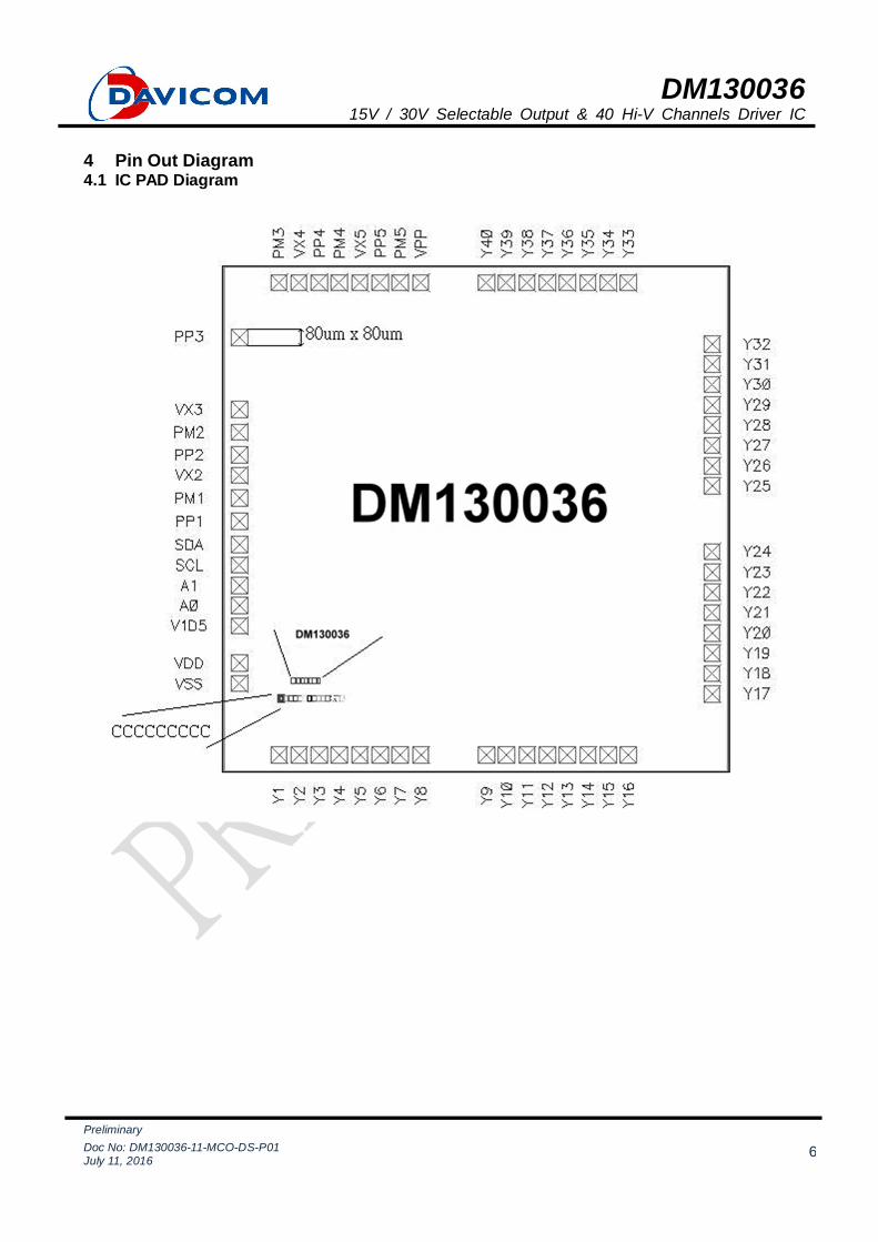
4 Pin Out Diagram4.1 IC PAD Diagram
DM13003615V / 30V Selectable Output & 40 Hi-V Channels Driver IC
PreliminaryDoc No: DM130036-11-MCO-DS-P01July 11, 2016
7
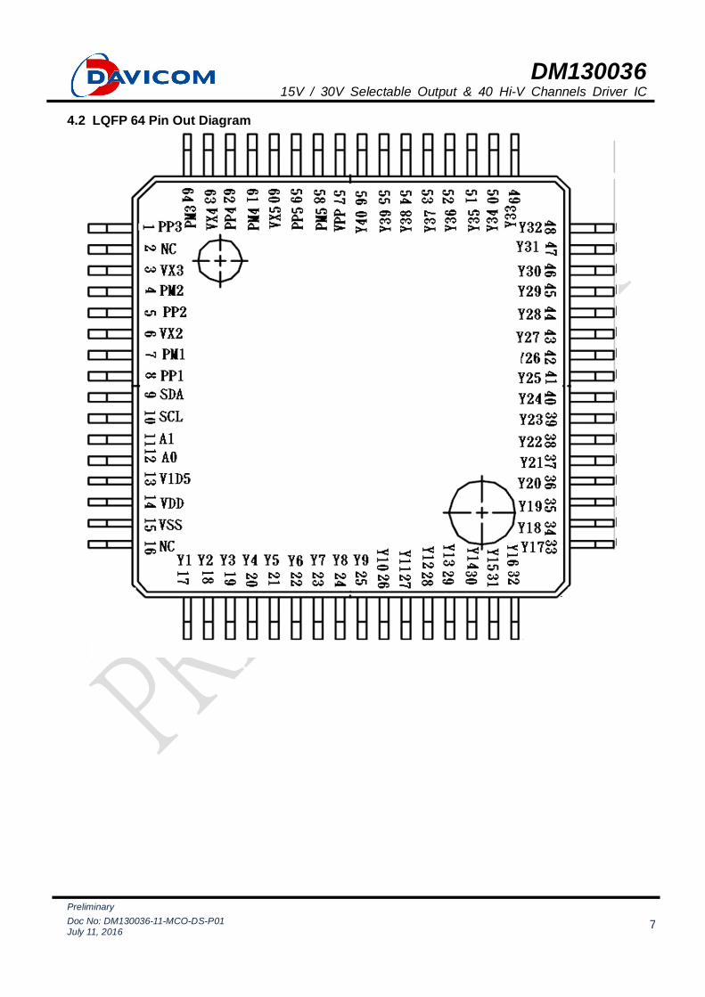
4.2 LQFP 64 Pin Out Diagram

DM13003615V / 30V Selectable Output & 40 Hi-V Channels Driver IC
PreliminaryDoc No: DM130036-11-MCO-DS-P01July 11, 2016
8
4.3 LFBGA 64 Pin out Diagram (Top View)

DM13003615V / 30V Selectable Output & 40 Hi-V Channels Driver IC
PreliminaryDoc No: DM130036-11-MCO-DS-P01July 11, 2016
9
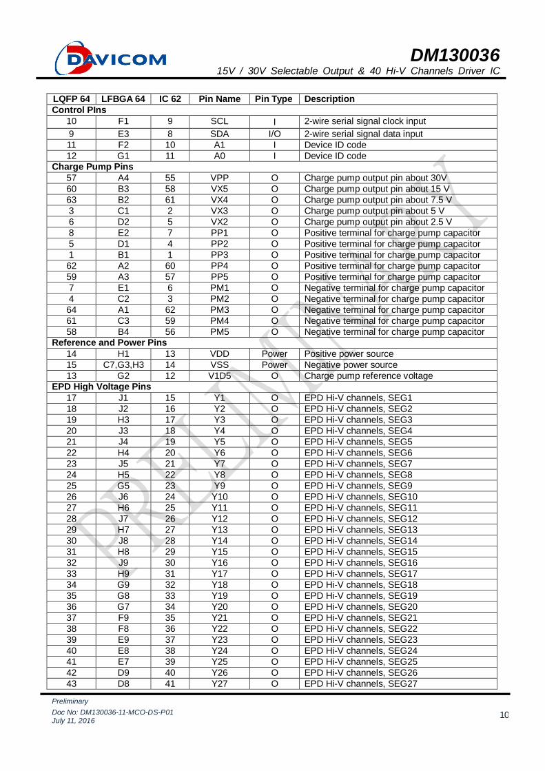
5 Pin DescriptionPIN NAME Description
SCL 2-wire serial signal clock inputSDA 2-wire serial signal data inputA1 Device ID codeA0 Device ID code
VPP Charge pump output pin about 30VVX5 Charge pump output pin about 15 VVX4 Charge pump output pin about 7.5 VVX3 Charge pump output pin about 5 VVX2 Charge pump output pin about 2.5 V
PP[1:5] Positive terminal for charge pump capacitorPM[1:5] Negative terminal for charge pump capacitorY[1:40] EPD Hi-V channelsVDD Positive power sourceVSS Negative power sourceV1D5 Charge pump reference voltage
Note:SCL & SDA need pull high resistor 4.7KΩ to VDD VID5 needs connect to 0.1uF to VSS
DM13003615V / 30V Selectable Output & 40 Hi-V Channels Driver IC
PreliminaryDoc No: DM130036-11-MCO-DS-P01July 11, 2016
10
LQFP 64 LFBGA 64 IC 62 Pin Name Pin Type DescriptionControl PIns
10 F1 9 SCL I 2-wire serial signal clock input9 E3 8 SDA I/O 2-wire serial signal data input11 F2 10 A1 I Device ID code12 G1 11 A0 I Device ID code
Charge Pump Pins57 A4 55 VPP O Charge pump output pin about 30V60 B3 58 VX5 O Charge pump output pin about 15 V63 B2 61 VX4 O Charge pump output pin about 7.5 V3 C1 2 VX3 O Charge pump output pin about 5 V6 D2 5 VX2 O Charge pump output pin about 2.5 V8 E2 7 PP1 O Positive terminal for charge pump capacitor5 D1 4 PP2 O Positive terminal for charge pump capacitor1 B1 1 PP3 O Positive terminal for charge pump capacitor62 A2 60 PP4 O Positive terminal for charge pump capacitor59 A3 57 PP5 O Positive terminal for charge pump capacitor7 E1 6 PM1 O Negative terminal for charge pump capacitor4 C2 3 PM2 O Negative terminal for charge pump capacitor64 A1 62 PM3 O Negative terminal for charge pump capacitor61 C3 59 PM4 O Negative terminal for charge pump capacitor58 B4 56 PM5 O Negative terminal for charge pump capacitor
Reference and Power Pins14 H1 13 VDD Power Positive power source15 C7,G3,H3 14 VSS Power Negative power source13 G2 12 V1D5 O Charge pump reference voltage
EPD High Voltage Pins17 J1 15 Y1 O EPD Hi-V channels, SEG118 J2 16 Y2 O EPD Hi-V channels, SEG219 H3 17 Y3 O EPD Hi-V channels, SEG320 J3 18 Y4 O EPD Hi-V channels, SEG421 J4 19 Y5 O EPD Hi-V channels, SEG522 H4 20 Y6 O EPD Hi-V channels, SEG623 J5 21 Y7 O EPD Hi-V channels, SEG724 H5 22 Y8 O EPD Hi-V channels, SEG825 G5 23 Y9 O EPD Hi-V channels, SEG926 J6 24 Y10 O EPD Hi-V channels, SEG1027 H6 25 Y11 O EPD Hi-V channels, SEG1128 J7 26 Y12 O EPD Hi-V channels, SEG1229 H7 27 Y13 O EPD Hi-V channels, SEG1330 J8 28 Y14 O EPD Hi-V channels, SEG1431 H8 29 Y15 O EPD Hi-V channels, SEG1532 J9 30 Y16 O EPD Hi-V channels, SEG1633 H9 31 Y17 O EPD Hi-V channels, SEG1734 G9 32 Y18 O EPD Hi-V channels, SEG1835 G8 33 Y19 O EPD Hi-V channels, SEG1936 G7 34 Y20 O EPD Hi-V channels, SEG2037 F9 35 Y21 O EPD Hi-V channels, SEG2138 F8 36 Y22 O EPD Hi-V channels, SEG2239 E9 37 Y23 O EPD Hi-V channels, SEG2340 E8 38 Y24 O EPD Hi-V channels, SEG2441 E7 39 Y25 O EPD Hi-V channels, SEG2542 D9 40 Y26 O EPD Hi-V channels, SEG2643 D8 41 Y27 O EPD Hi-V channels, SEG27

DM13003615V / 30V Selectable Output & 40 Hi-V Channels Driver IC
PreliminaryDoc No: DM130036-11-MCO-DS-P01July 11, 2016
11
44 C9 42 Y28 O EPD Hi-V channels, SEG2845 C8 43 Y29 O EPD Hi-V channels, SEG2946 B8 44 Y30 O EPD Hi-V channels, SEG3047 B9 45 Y31 O EPD Hi-V channels, SEG3148 A9 46 Y32 O EPD Hi-V channels, SEG3249 A8 47 Y33 O EPD Hi-V channels, SEG3350 A7 48 Y34 O EPD Hi-V channels, SEG3451 B9 49 Y35 O EPD Hi-V channels, SEG3551 A6 50 Y36 O EPD Hi-V channels, SEG3653 B6 51 Y37 O EPD Hi-V channels, background54 A5 52 Y38 O EPD Hi-V channels, background55 B5 53 Y39 O EPD Hi-V channels, common56 C5 54 Y40 O EPD Hi-V channels, common
Others2,16 NC N/A
Note: O = output, I = input, I/O = bidirection
DM13003615V / 30V Selectable Output & 40 Hi-V Channels Driver IC
PreliminaryDoc No: DM130036-11-MCO-DS-P01July 11, 2016
12
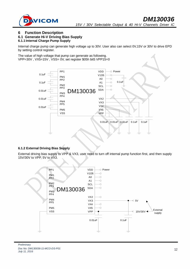
6 Function Description6.1 Generate Hi-V Driving Bias Supply6.1.1 Internal Charge Pump SupplyInternal charge pump can generate high voltage up to 30V. User also can select 0V,15V or 30V to drive EPDby setting control register.
The value of high voltage that pump can generate as following.VPP=30V , VX5=15V , VSS= 0V, set register $05h bit5 VPP15=0
PP5
PM5
VX3VX4VX5VPP
A0A1
SCLSDA
VSS
VDD Power
0.1uF
0.01uF
0.01uF
0.01uF
0.01uF 0.01uF 0.01uF 0.1uF
DM130036
V1D50.1uF
VX2
0.1uF
PP4
PM4
PP3
PM3
PP2
PM2
PP1
PM1
0.1uF
6.1.2 External Driving Bias SupplyExternal driving bias supply to VPP & VX3, user need to turn off internal pump function first, and then supply15V/30V to VPP, 5V to VX3.
PP5
PM5
VX3VX4VX5VPP
A0A1
SCLSDA
VSS
VDD Power
0.01uF 0.1uF
DM130036
V1D5
VX2PP4
PM4
PP3
PM3
PP2
PM2
PP1
PM1
15V/30V
5V
Externalsupply

DM13003615V / 30V Selectable Output & 40 Hi-V Channels Driver IC
PreliminaryDoc No: DM130036-11-MCO-DS-P01July 11, 2016
13
6.2 Multi-drivers ApplicationThe host device with 2-wire serial interface can control DM130036. (A1,A0) pins correspond to the ID setting(Maximum support 4 chips). See the following figure for setting ID option.
PP5
PM5
VX3VX4VX5VPP
A0A1
SCLSDAVSS
VDD
0.1uF
0.01uF
0.01uF
0.01uF
C1=0.01uFC2=0.01uFC3=0.01uFC4=0.1uFC5=0.1uFC6=0.1uF
DM130036
V1D50.1uF
VX2PP4
PM4
PP3
PM3
PP2
PM2
PP1
PM1
C1 C2 C3 C4 C5
VX3VX4VX5VPP
A0A1
SCLSDA
VDD
DM130036
V1D5
VX2
VX3VX4VX5VPP
A0A1
SCLSDA
VDD
DM130036
V1D5
VX2
VX3VX4VX5VPP
A0A1
SCLSDA
VDD
DM130036
V1D5
VX2
VSS
VSS
VSS
Pow
erSC
LSD
AID 11
ID 01
ID 10
ID 00
C6
DM13003615V / 30V Selectable Output & 40 Hi-V Channels Driver IC
PreliminaryDoc No: DM130036-11-MCO-DS-P01July 11, 2016
14
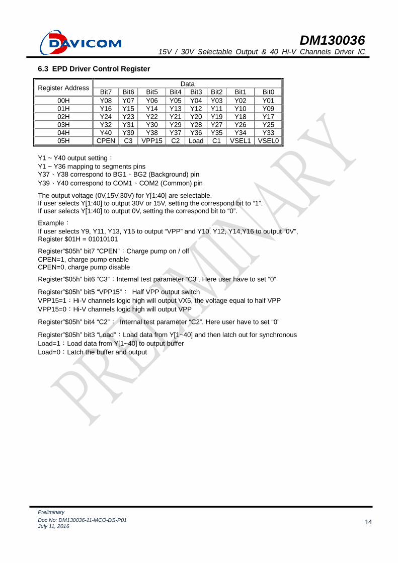
6.3 EPD Driver Control Register
Y1 ~ Y40 output setting:Y1 ~ Y36 mapping to segments pinsY37、Y38 correspond to BG1、BG2 (Background) pinY39、Y40 correspond to COM1、COM2 (Common) pin
The output voltage (0V,15V,30V) for Y[1:40] are selectable.If user selects Y[1:40] to output 30V or 15V, setting the correspond bit to “1”.If user selects Y[1:40] to output 0V, setting the correspond bit to “0”.
Example:If user selects Y9, Y11, Y13, Y15 to output “VPP” and Y10, Y12, Y14,Y16 to output “0V”,Register $01H = 01010101
Register”$05h” bit7 “CPEN”:Charge pump on / offCPEN=1, charge pump enableCPEN=0, charge pump disable
Register”$05h” bit6 “C3”:Internal test parameter “C3”. Here user have to set “0”
Register”$05h” bit5 “VPP15”: Half VPP output switchVPP15=1:Hi-V channels logic high will output VX5, the voltage equal to half VPPVPP15=0:Hi-V channels logic high will output VPP
Register”$05h” bit4 “C2”: Internal test parameter “C2”. Here user have to set “0”
Register”$05h” bit3 “Load”:Load data from Y[1~40] and then latch out for synchronousLoad=1:Load data from Y[1~40] to output bufferLoad=0:Latch the buffer and output
Register Address DataBit7 Bit6 Bit5 Bit4 Bit3 Bit2 Bit1 Bit0
00H Y08 Y07 Y06 Y05 Y04 Y03 Y02 Y0101H Y16 Y15 Y14 Y13 Y12 Y11 Y10 Y0902H Y24 Y23 Y22 Y21 Y20 Y19 Y18 Y1703H Y32 Y31 Y30 Y29 Y28 Y27 Y26 Y2504H Y40 Y39 Y38 Y37 Y36 Y35 Y34 Y3305H CPEN C3 VPP15 C2 Load C1 VSEL1 VSEL0
DM13003615V / 30V Selectable Output & 40 Hi-V Channels Driver IC
PreliminaryDoc No: DM130036-11-MCO-DS-P01July 11, 2016
15
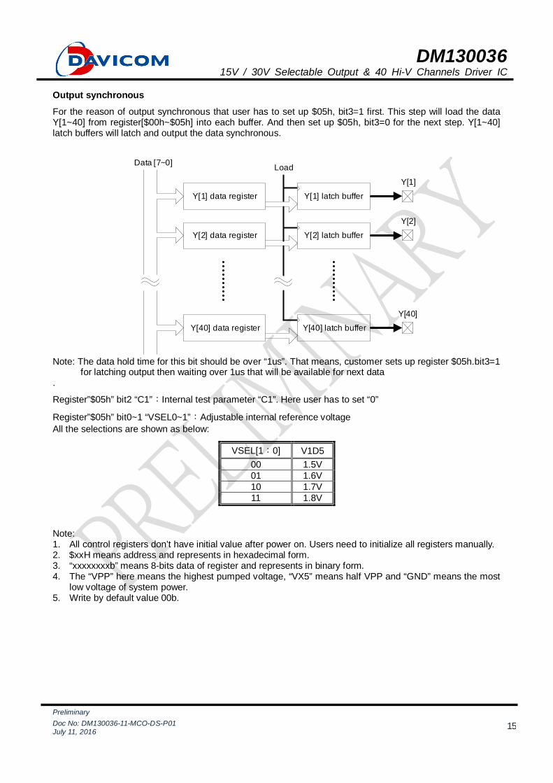
Output synchronousFor the reason of output synchronous that user has to set up $05h, bit3=1 first. This step will load the dataY[1~40] from register[$00h~$05h] into each buffer. And then set up $05h, bit3=0 for the next step. Y[1~40]latch buffers will latch and output the data synchronous.
Y[1] data register
Y[2] data register
Y[40] data register
Y[1] latch buffer
Y[2] latch buffer
Y[40] latch buffer
LoadData [7~0]
Y[1]
Y[2]
Y[40]
Note: The data hold time for this bit should be over “1us”. That means, customer sets up register $05h.bit3=1for latching output then waiting over 1us that will be available for next data
.
Register”$05h” bit2 “C1”:Internal test parameter “C1”. Here user has to set “0”
Register”$05h” bit0~1 “VSEL0~1”:Adjustable internal reference voltageAll the selections are shown as below:
Note:1. All control registers don’t have initial value after power on. Users need to initialize all registers manually.2. $xxH means address and represents in hexadecimal form.3. “xxxxxxxxb” means 8-bits data of register and represents in binary form.4. The “VPP” here means the highest pumped voltage, “VX5” means half VPP and “GND” means the most
low voltage of system power.5. Write by default value 00b.
VSEL[1:0] V1D500 1.5V01 1.6V10 1.7V11 1.8V

DM13003615V / 30V Selectable Output & 40 Hi-V Channels Driver IC
PreliminaryDoc No: DM130036-11-MCO-DS-P01July 11, 2016
16
6.4 Control Signal Waveform6.4.1 Format of One ByteThis byte can be 00H~05H, see 6.3 EPD driver control register
SDA
SCL
Start Bit Device ID code ACK Register address ACK Data ACK Stop Bit
AckBit0Bit1Bit2Bit3Bit4Bit5Bit6Bit7SDA
SCL
start bit AckDevice ID Code
AckBit0Bit1Bit2Bit3Bit4Bit5Bit6Bit7SDA
SCL
AckRegister Address
AckBit0Bit1Bit2Bit3Bit4Bit5Bit6Bit7SDA
SCL
AckData stop bit
Host deviceinput mode
Host deviceinput mode
Host deviceinput mode
1us 0.8us
1us50ns50ns
0.8us 1us1us50ns50ns
Note: Timing diagram above is when SCL=500KHz
Device ID code:ID code defined by (A0&A1) pins. See P9 multi-driver application. Control signal input 8-bits “111100A1,A0”(A1,A0)=00 or 01 or 10 or 11 then only matched driver will operate.
Register address:The control registers are from $00H~$05H. The control signal is after Device ID code.
Data of register:Definition of all control registers, see 6.3 EPD driver control register.

DM13003615V / 30V Selectable Output & 40 Hi-V Channels Driver IC
PreliminaryDoc No: DM130036-11-MCO-DS-P01July 11, 2016
17
Condition settingPerform with one driver IC and ID code (A1,A0)=00
Operating flow of one byteCondition:Perform one driverID code(A1,A0)=00
Host device inputControl signal
Device ID code
Host device inputControl signal
Start bit
Host device checkDevice ID code ack
Pass
Host deviceTimeout functionFor Ack feedback
Fail
Pass
Host device inputControl signal
Register address
Host device checkRegister address ack
Pass
Host deviceTimeout functionFor Ack feedback
Fail
Pass
Host device inputControl signal
Data of register
Host device checkData of register ack
Pass
Host deviceTimeout functionFor Ack feedback
Fail
Pass
Host device inputControl signal
Stop bit
ACKfeedback Timeout
Fail
Note:1. According to operating flow above, host device needs to switch the pin to input-mode which connects to
SDA while ACK feedback. Also check ACK feedback “Low” it means current byte transmission pass.2. All the timing of pulse-width in operating flow above represents the minimum acceptable value.3. Operating flow above is only for reference. For actual situation, please refer to E-paper spec.
DM13003615V / 30V Selectable Output & 40 Hi-V Channels Driver IC
PreliminaryDoc No: DM130036-11-MCO-DS-P01July 11, 2016
18
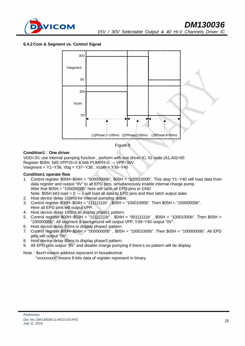
6.4.2 Com & Segment vs. Control Signal
Vcom
30V
0V
(1)Phase1=100ms
Vsegment
30V
0V
(2)Phase2=50ms (3)Phase3=80ms
Figure 9
Condition1:One driverVDD=3V, use internal pumping function , perform with one driver IC, ID code (A1,A0)=00Register $05H. bit5 VPP15=0 & bit6 PUMPH=0 → VPP=30VVsegment = Y1~Y36, Vbg = Y37~Y38 , Vcom = Y39~Y40
Condition1 operate flow1. Control register $00H~$04H = “00000000b”, $05H = “10001000b”. This step Y1~Y40 will load data from
data register and output “0V” to all EPD pins, simultaneously enable internal charge pump.After that $05H = “10000000b” here will latch all EPD pins to GNDNote: $05H bit3 load = 0 → 1 will load all data to EPD pins and then latch output state.
2. Host device delay 100ms for internal pumping stable.3. Control register $00H~$04H = “11111111b” , $05H = “10001000b”. Then $05H = “10000000b”.
Here all EPD pins will output VPP.4. Host device delay 100ms to display phase1 pattern.5. Control register $00H~$03H = “11111111b” , $04H = “00111111b” , $05H = “10001000b”. Then $05H =
“10000000b”. All segment & background will output VPP, Y39~Y40 output “0V”.6. Host device delay 50ms to display phase2 pattern.7. Control register $00H~$04H = “00000000b” , $05H = “10001000b”. Then $05H = “10000000b”. All EPD
pins will output “0V”.8. Host device delay 80ms to display phase3 pattern.9. All EPD pins output “0V” and disable charge pumping if there’s no pattern will be display.
Note:$xxH means address represent in hexadecimal. “xxxxxxxxb” means 8-bits data of register represent in binary.

DM13003615V / 30V Selectable Output & 40 Hi-V Channels Driver IC
PreliminaryDoc No: DM130036-11-MCO-DS-P01July 11, 2016
19
Condition:VDD=3V, perform one driver ICID code(A1,A0)=00, VPP=30V
Y1~Y40 output 0Vand pump ebable
Control register $00~$04H= 00H
$05H = 88 then to 80H
Host deviceDelay 100ms forpumping stability
Control register $00~$04H= FFH
$05H = 88 then to 80H
Phase1holding 100ms
Control register$00~$03H = FFH
$04H = 3FH$05H = 88 then to 80H
Phase2holding 50ms
Control register $00~$04H= 00H
$05H = 88 then to 80H
Phase3holding 80ms
Phase1
Phase2
Phase3
Display next pattern?
All EPD pins output VSSthen disable charge
pumpingControl register $00~$04H
= 00H$05H = 08 then to 00H
NO
YES
New patternIC wake up
Trigger Stop mode
Pattern 1
Initialize setting
DM13003615V / 30V Selectable Output & 40 Hi-V Channels Driver IC
PreliminaryDoc No: DM130036-11-MCO-DS-P01July 11, 2016
20
Condition2:Cascade four drivers
VDD=3V , perform with four drivers, Set one driver to be the pumping source and others supply from thisdriver.
Register $05H. bit5 VPP15=0 , bit6 PUMPH=0 → VPP=30VVsegment including Y1~Y36 , Vcom = Y37~Y38 , Vbg = Y39~Y40
Condition2 operate flow1. ID[00] Control register $00H~$04H = “00000000b”, $05H = “00000000b”. This step Y1~Y40 will load data
from data register and output “0V” to all EPD pins simultaneously.After that $05H = “00001000b” here will latch all EPD pins to “0V”.Note! $05H bit3 load = 1 → 0 will load all data to EPD pins and then latch output state.
2. ID[01~11] follow step1 to initialize all EPD pins to output “0V”3. ID[00] register $05H = “10000000b” to enable charge pump and take ID[00] as pumping source others IC
set up supply from external source.4. Host device delay 100ms for internal pumping stability.5. ID[00~11] Control register $00H~$04H = “11111111b” , *ID[00] $05H = “10001000b” , ID[01~11] $05H =
“00001000b”. Then ID[00] $05H = “10000000b” ID[01~11] $05H = “00000000b”. Here all EPD pins willoutput VPP.
6. Host device delay 100ms to display phase1 pattern.7. ID[00~11] Control register $00H~$03H = “11111111b” , $04H = “11111100b” , *ID[00] $05H = “10001000b” ,
ID[01~11] $05H = “00001000b”. Then ID[00] $05H = “10000000b” , ID[01~11] $05H = “00000000b”. Allsegment will output VPP, but Y39~Y40 output “0V”.
8. Host device delay 50ms to display phase2 pattern.9. ID[00~11] Control register $00H~$04H = “00000000b” , *ID[00] $05H = “10001000b” , ID[01~11] $05H =
“00001000b”. Then ID[00] $05H = “10000000b” , ID[01~11] $05H = “00000000b”. All EPD pins will output“0V”.
10. Host device delay 80ms to display phase3 pattern.11. All EPD pins output “0V” and disable charge pumping if there’s no pattern will be display.
Note:$xxH means address and represent in hexadecimal form. “xxxxxxxxb” means 8-bits data and represents in binary form.

DM13003615V / 30V Selectable Output & 40 Hi-V Channels Driver IC
PreliminaryDoc No: DM130036-11-MCO-DS-P01July 11, 2016
21
Condition2:(4 drivers)2-wires serial modeperform four driversVDD=3VVPP=30V
ID[00~11] Y1~Y40output 0V
ID[00] Control register$00~$04H = 00H
$05H = 08 then to 00H
Host deviceDelay 100ms forpumping stability
ID[00] Control register$00~$04H = FFH
$05H = 88 then to 80H
Phase1holding 100ms
ID[00] Control register$00~$03H = FFH
$04H = 3FH$05H = 88 then to 80H
Phase2holding 50ms
ID[00] Control register$00~$04H = 00H
$05H = 88 then to 80H
Phase3holding 80ms
Initialize setting
Phase1
Phase2
Phase3
Display next pattern?
ID[00] Control register$00~$04H = 00H
$05H = 08 then to 00H
NO
Pattern1YES
New pattern
ID[01] Control register$00~$04H = 00H
$05H = 08 then to 00H
ID[10] Control register$00~$04H = 00H
$05H = 08 then to 00H
ID[11] Control register$00~$04H = 00H
$05H = 08 then to 00H
ID[00] Control register$05H = 80, pump enable
ID[01] Control register$00~$04H = FFH
$05H = 08 then to 00H
ID[10] Control register$00~$04H = FFH
$05H = 08 then to 00H
ID[11] Control register$00~$04H = FFH
$05H = 08 then to 00H
ID[01] Control register$00~$0EH = FFH
$04H = 3FH$05H = 08 then to 00H
ID[10] Control register$00~$0EH = FFH
$04H = 3FH$05H = 08 then to 00H
ID[11] Control register$00~$0EH = FFH
$04H = 3FH$05H = 08 then to 00H
ID[01] Control register$00~$04H = 00H
$05H = 08 then to 00H
ID[10] Control register$00~$0FH = 04H
$05H = 08 then to 00H
ID[11] Control register$00~$04H = 00H
$05H = 08 then to 00H
ID[01] Control register$00~$04H = 00H
$05H = 08 then to 00H
ID[10] Control register$00~$04H = 00H
$05H = 08 then to 00H
ID[11] Control register$00~$04H = 00H
$05H = 08 then to 00H
ID[00~11] All IC keepin stop mode
DM13003615V / 30V Selectable Output & 40 Hi-V Channels Driver IC
PreliminaryDoc No: DM130036-11-MCO-DS-P01July 11, 2016
22
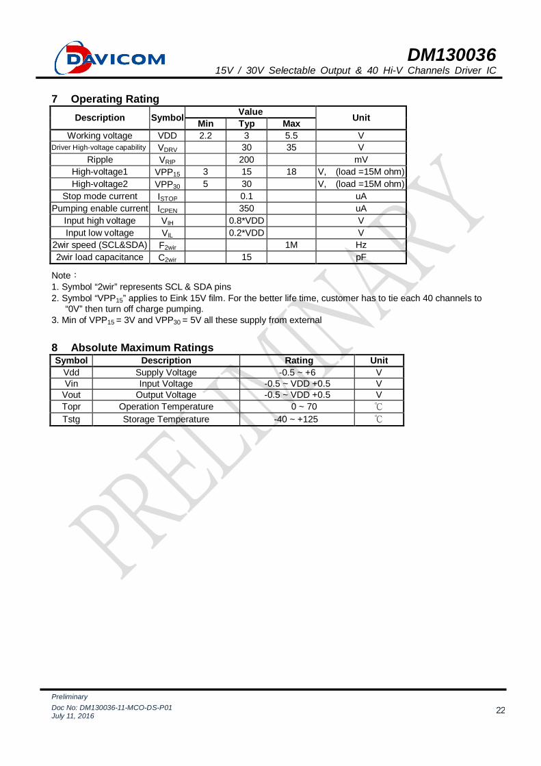
7 Operating RatingDescription Symbol Value UnitMin Typ Max
Working voltage VDD 2.2 3 5.5 VDriver High-voltage capability VDRV 30 35 V
Ripple VRIP 200 mVHigh-voltage1 VPP15 3 15 18 V, (load =15M ohm)High-voltage2 VPP30 5 30 V, (load =15M ohm)
Stop mode current ISTOP 0.1 uAPumping enable current ICPEN 350 uA
Input high voltage VIH 0.8*VDD VInput low voltage VIL 0.2*VDD V
2wir speed (SCL&SDA) F2wir 1M Hz2wir load capacitance C2wir 15 pF
Note:1. Symbol “2wir” represents SCL & SDA pins2. Symbol “VPP15” applies to Eink 15V film. For the better life time, customer has to tie each 40 channels to
“0V” then turn off charge pumping.3. Min of VPP15 = 3V and VPP30 = 5V all these supply from external
8 Absolute Maximum RatingsSymbol Description Rating Unit
Vdd Supply Voltage -0.5 ~ +6 VVin Input Voltage -0.5 ~ VDD +0.5 V
Vout Output Voltage -0.5 ~ VDD +0.5 VTopr Operation Temperature 0 ~ 70 ℃
Tstg Storage Temperature -40 ~ +125 ℃

DM13003615V / 30V Selectable Output & 40 Hi-V Channels Driver IC
PreliminaryDoc No: DM130036-11-MCO-DS-P01July 11, 2016
23
8.1 AC Characteristic
Tst
SCL
SDA
Tst Thd
Tckh Tckl
Tck
Thd
Tst Thd
TzdTdz
every 9th bit ACKb
Master drive Hi-ZSDA will drive low
Parameter Details Min Typ Max unitsTck Clock cycle time 1 usTckl Clock low time 400 nsTckh Clock high time 400 nsTst Setup time 100 nsThd Hold time 100 nsTdz Clock low to data Hi-z delay 80 nsTzd Clock low to data drive delay 80 ns
8.2 HVPAD DrivingParameter Conditions Vout Min Typ Max units
Roh Y1 ~ Y36, VPP=16V
Vout=15V
7.1 K-ohm
Roh Y37 ~ Y38, VPP=16V 4.6 K-ohm
Roh Y39 ~ Y40, VPP=16V 4.4 K-ohm
Roh Y1 ~ Y36, VPP=32V
Vout =30V
5.1 K-ohm
Roh Y37 ~ Y38, VPP=32V 3.2 K-ohm
Roh Y39~ Y40, VPP=32V 3.4 K-ohm
Note : Roh represents internal equivalent resistor at driving capability.
DM13003615V / 30V Selectable Output & 40 Hi-V Channels Driver IC
PreliminaryDoc No: DM130036-11-MCO-DS-P01July 11, 2016
24
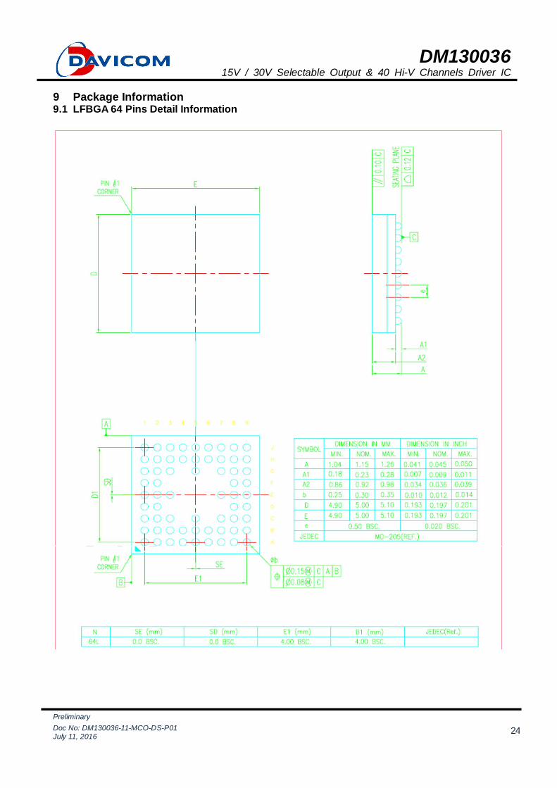
9 Package Information9.1 LFBGA 64 Pins Detail Information
DM13003615V / 30V Selectable Output & 40 Hi-V Channels Driver IC
PreliminaryDoc No: DM130036-11-MCO-DS-P01July 11, 2016
25
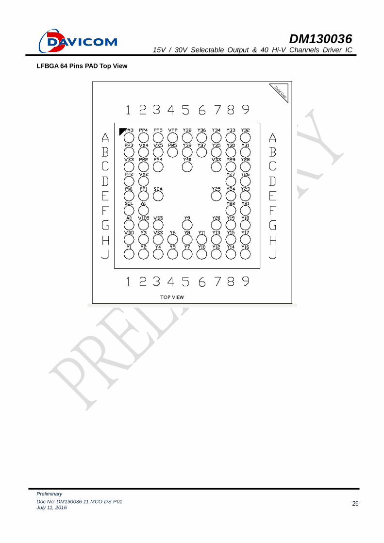
LFBGA 64 Pins PAD Top View

DM13003615V / 30V Selectable Output & 40 Hi-V Channels Driver IC
PreliminaryDoc No: DM130036-11-MCO-DS-P01July 11, 2016
26
9.2 LQFP 64 Pins Detail Information
LQFP 64 Pins PAD Top View

DM13003615V / 30V Selectable Output & 40 Hi-V Channels Driver IC
PreliminaryDoc No: DM130036-11-MCO-DS-P01July 11, 2016
27
9.3 COF InformationDM130036 COF module
DM130036 COF layout
DM13003615V / 30V Selectable Output & 40 Hi-V Channels Driver IC
PreliminaryDoc No: DM130036-11-MCO-DS-P01July 11, 2016
28
10 Ordering InformationPart Number Pin Count PackageDM130036W - Wafer (Pb-Free)
DM130036WB - Wafer + Gold bump(Pb-Free)
DM130036 64 Dice (Pb-Free)
DM130036B 64 Dice + Gold bump(Pb-Free)
DM130036GP 64 LFBGA 64L (Pb-Free)DM130036EP 64 LQFP 64L (Pb-Free)DM130036C 159 COF (Roll) (Pb-Free)DM130036P 159 COF (Tray) (Pb-Free)
DisclaimerThe information appearing in this publication isbelieved to be accurate. Integrated circuits sold byDAVICOM Semiconductor are covered by thewarranty and patent indemnification provisionsstipulated in the terms of sale only. DAVICOM makesno warranty, express, statutory, implied or bydescription regarding the information in this publicationor regarding the information in this publication orregarding the freedom of the described chip(s) frompatent infringement. FURTHER, DAVICOM MAKESNO WARRANTY OF MERCHANTABILITY ORFITNESS FOR ANY PURPOSE. DAVICOM reservesthe right to halt production or alter the specificationsand prices at any time without notice. Accordingly, thereader is cautioned to verify that the data sheets andother information in this publication are current beforeplacing orders. Products described herein areintended for use in normal commercial applications.Applications involving unusual environmental orreliability requirements, e.g. military equipment ormedical life support equipment, are specifically notrecommended without additional processing byDAVICOM for such applications.
Please note that application circuits illustrated inthis document are for reference purposes only.
DAVICOM’s terms and conditions printed on theorder acknowledgment govern all sales byDAVICOM. DAVICOM will not be bound by anyterms inconsistent with these unless DAVICOMagrees otherwise in writing. Acceptance of thebuyer’s orders shall be based on these terms.
Company OverviewDAVICOM Semiconductor Inc. develops andmanufactures integrated circuits for integrationinto data communication products. Our missionis to design and produce IC products that are theindustry’s best value for Data, Audio, Video, andInternet/Intranet applications. To achieve thisgoal, we have built an organization that is able todevelop chipsets in response to the evolvingtechnology requirements of our customers whilestill delivering products that meet their costrequirements.
ProductsWe offer only products that satisfy highperformance requirements and which arecompatible with major hardware and softwarestandards. Our currently available and soon tobe released products are based on ourproprietary designs and deliver high quality, highperformance chipsets that comply with modemcommunication standards and Ethernetnetworking standards. For customizedproducts, please contact to Davicom’s sales
Contact WindowsFor additional information about DAVICOM products, contact the Sales department at:HeadquartersHsin-chu Office:No.6, Li-Hsin 6th Rd.,Hsinchu Science Park,Hsin-chu City 300, Taiwan, R.O.C.TEL: +886-3-5798797FAX: +886-3-5646929MAIL: [email protected]: http://www.davicom.com.tw
WARNINGConditions beyond those listed for the absolute maximum rating may destroy or damage the products. In addition, conditions for sustained periods atnear the limits of the operating ranges will stress and may temporarily (or permanently) affect and damage structure, performance and function.