4 th module. pic microcontrollers are basically risc microcontrollers with very small instruction...
TRANSCRIPT
4th MODULE
PIC
• Microcontrollers are basically RISC microcontrollers with very small instruction set of only 35 instructions and a two-stage pipeline concept fetch and execution of instructions. As a result, all instructions execute in a single cycle except for program branches.
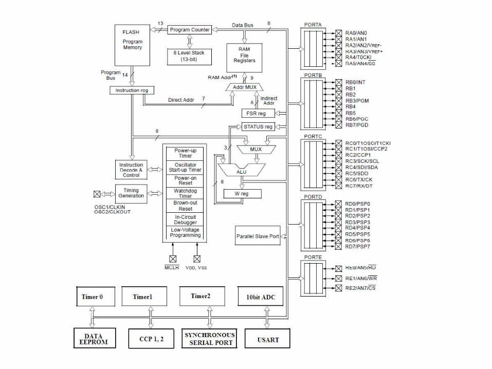
• PIC 16F877 is a 40-pin 8-Bit CMOS FLASH Microcontroller . • 16F877 comes with 3 operating speeds with 4, 8, or 20 MHz clock input.• It has two types of internal memories .One is program memory and the
other is data memory. • Program memory is provided by 8K words (or 8K*14 bits) of FLASH
Memory, and data memory has two sources. • One type of data memory is a 368-byte RAM (random access memory)
and the other is256-byte EEPROM (Electrically erasable programmable ROM).
• The core features include interrupt up to 14 sources, power saving SLEEP mode, a single 5V supply and In-Circuit Serial Programming (ICSP) capability
• Power consumption is less than 2 mA in 5V operating condition.
SALIENT FEATURES
• Speed :• When operated at its maximum clock rate a
PIC executes most of its instructions in 0.2 s or five instructions per microsecond
• Instruction set Simplicity :• The instruction set is so simple that it consists
of only just 35 instructions
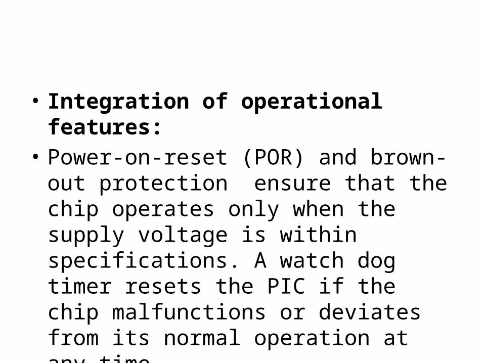
• Integration of operational features:• Power-on-reset (POR) and brown-out
protection ensure that the chip operates only when the supply voltage is within specifications. A watch dog timer resets the PIC if the chip malfunctions or deviates from its normal operation at any time.
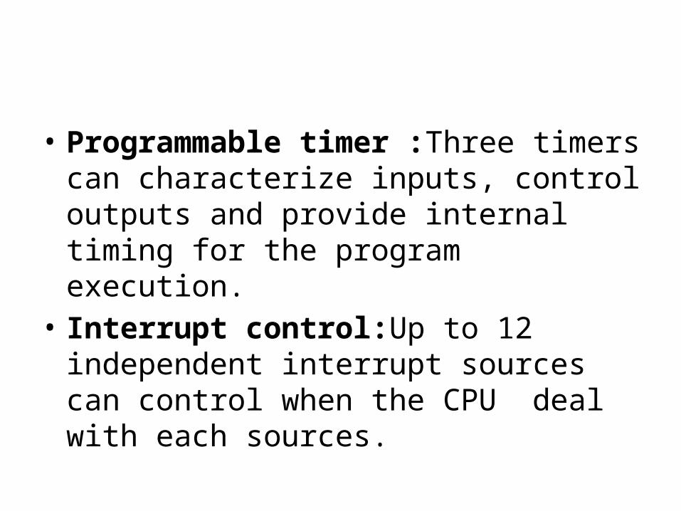
• Programmable timer :Three timers can characterize inputs, control outputs and provide internal timing for the program execution.
• Interrupt control:Up to 12 independent interrupt sources can control when the CPU deal with each sources.
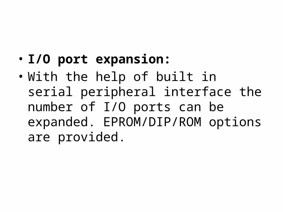
• I/O port expansion:• With the help of built in serial peripheral
interface the number of I/O ports can be expanded. EPROM/DIP/ROM options are provided.
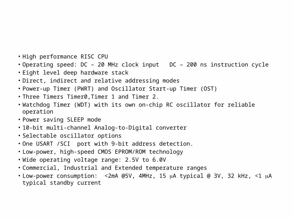
• High performance RISC CPU• Operating speed: DC – 20 MHz clock input DC – 200 ns instruction cycle• Eight level deep hardware stack• Direct, indirect and relative addressing modes• Power-up Timer (PWRT) and Oscillator Start-up Timer (OST)• Three Timers Timer0,Timer 1 and Timer 2.• Watchdog Timer (WDT) with its own on-chip RC oscillator for reliable operation• Power saving SLEEP mode• 10-bit multi-channel Analog-to-Digital converter• Selectable oscillator options• One USART /SCI port with 9-bit address detection.• Low-power, high-speed CMOS EPROM/ROM technology• Wide operating voltage range: 2.5V to 6.0V• Commercial, Industrial and Extended temperature ranges• Low-power consumption: <2mA @5V, 4MHz, 15 A typical @ 3V, 32 kHz, <1 A typical
standby current
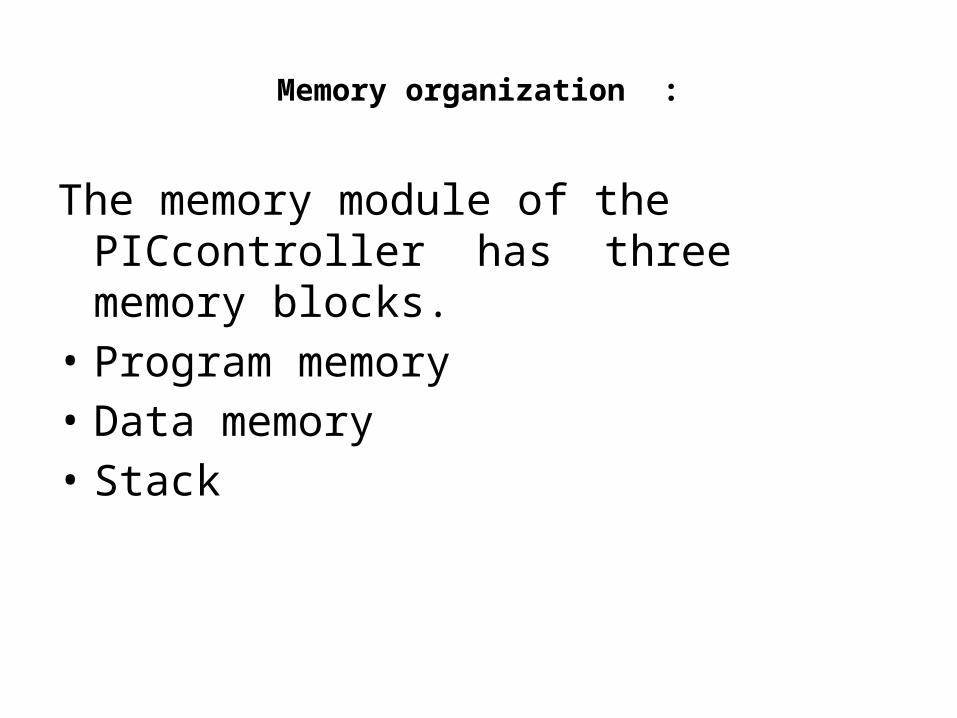
Memory organization :
The memory module of the PICcontroller has three memory blocks.
• Program memory• Data memory • Stack
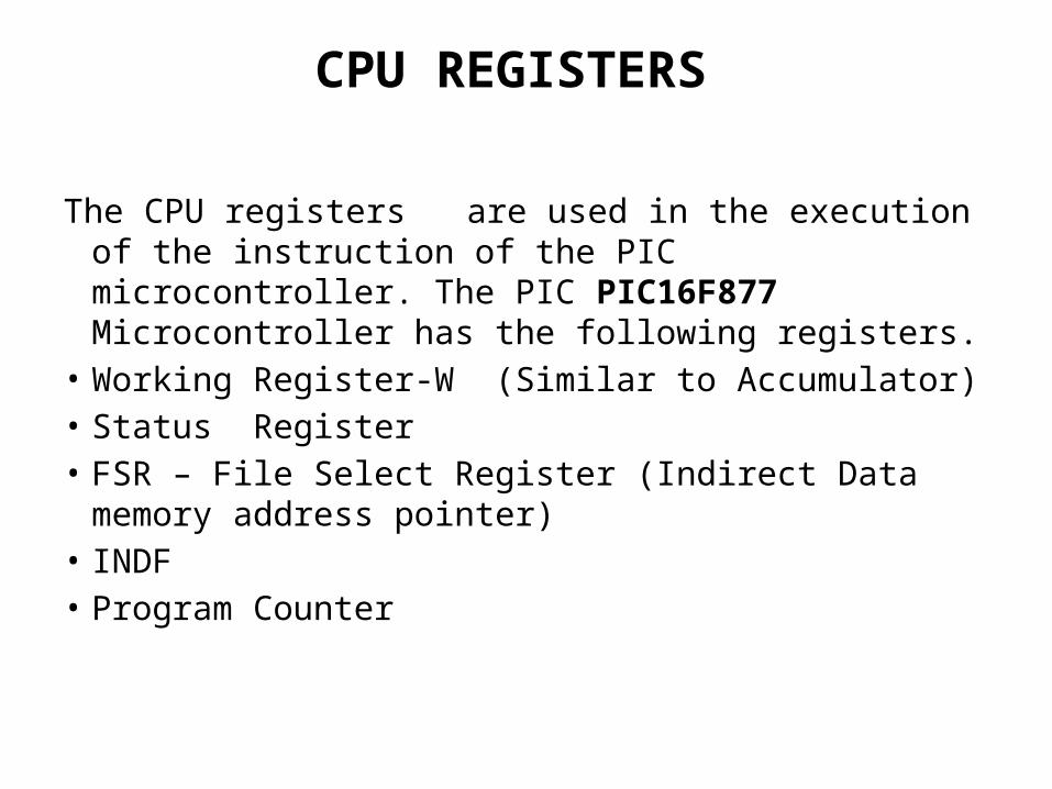
CPU REGISTERS
The CPU registers are used in the execution of the instruction of the PIC microcontroller. The PIC PIC16F877 Microcontroller has the following registers.
• Working Register-W (Similar to Accumulator)• Status Register• FSR – File Select Register (Indirect Data memory
address pointer)• INDF• Program Counter
Working Register is used by many instructions as the source of an operand. It also serves as the destination for the result of instruction execution and it is similar to accumulator in other cs and ps.
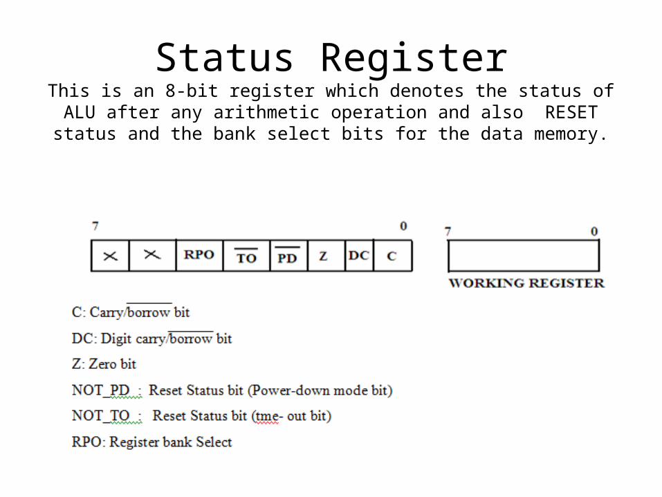
Status Register• This is an 8-bit register which denotes the status of ALU after any arithmetic
operation and also RESET status and the bank select bits for the data memory.
• C: Carry/borrow bit• DC: Digit carry/borrow bit• Z: Zero bit• NOT_PD : Reset Status bit (Power-down mode bit)• NOT_TO : Reset Status bit (tme- out bit)• RPO: Register bank Select• The bits 7 and 6 of Status Register are unused by 16c6x/7x. The ‘C’ bit is set
when two 8-bit operands are added together and a 9-bit result occurs. This 9-bit is placed in the carry bit.
• The DC or Digit carry bit indicates that a carry from the lower 4 bits occurred during an 8-bit addition.
Status RegisterThis is an 8-bit register which denotes the status of ALU after any arithmetic
operation and also RESET status and the bank select bits for the data memory.
FSR – (File Select Register)
• It is the pointer used for indirect addressing. In the indirect addressing mode the 8-bit register file address is first written into FSR. It is a special purpose register that serves as an address pointer to any address through out the entire register file.
INDF – (Indirect File)
It is not a physical register addressing but this INDF will cause indirect addressing. Any instruction using the INDF register actually access the register pointed to by the FSR.
PARALLEL I/O Ports
• Most of the PIC16cx/7x family controllers have 33 I/O lines and five I/O ports They are PORT A, PORT B, PORT C , PORT D and PORT E.
• Port A is a 6-bit wide bi-directional port. Its data direction register is TRISA setting TRISA bit to 1 will make the corresponding PORT A Pin an input. Clearing a TRIS a bit will make the corresponding pin as an output.
• PORT B is an 8-bit wide, bi-directional port. Four of the PORT B pins RB7 – RB4 have an interrupt-on- change feature. Only the pins configured as inputs can cause this interrupt to occur.
• Port C is an 8-bit wide, bidirectional port. Bits of the TRISC Register determine the function of its pins. Similar to other ports, a logic one 1 in the TRISC Register configures the appropriate port pin as an input.
• PORT D: is an 8-bit wide bi-directional port. In addition to I/O port, Port D also works as 8-bit parallel slave port or microprocessor port. When control bit PSPMODE (TRISE:4) is set.
• PORT E: is a 3-bit bi-directional port. Port E bits are multiplexed with analog inputs of ADC and they serve as control signals (RD , WR, CS) for parallel slave port mode of operation.
TIMER MODULES
• There are three completely independent Timers available in PIC 16F8XX Microcontrollers. They are
• Timer 0 - The Timer 0 module is a simple 8-bit overflow counter.
• Timer1 - When operating as a counter (external clock source), the counter can either operate synchronized to the device or asynchronously to the device. Asynchronous operation allows Timer1 to operate during sleep, which is useful for applications that require a real-time clock as well as the power savings of SLEEP mode.
• Timer 2 : is an 8-bit timer with a programmable prescaler and a programmable postscaler, as well as an 8-bit Period Register (PR2). Timer 2 can be used with the CCP module (in PWM mode) as well as the Baud Rate Generator for the Synchronous Serial Port (SSP).
CCP (Capture-Compare –PWM)
The CCP module(s) can operate in one of three modes 16-bit capture, 16-bit compare, or up to 10-bit Pulse Width Modulation (PWM)
INTERRUPTS
The PIC16F8XX family has up to 11 sources of interrupt. The interrupt control register (INTCON) records individual interrupt requests in flag bits. It also has individual and global interrupt enable bits.
WATCH DOG TIMER (WDT)
The Watchdog Timer is a free running on-chip RC oscillator which does not require any external components. This RC oscillator is separate from the RC oscillator of the OSC1/CLKIN pin. That means that the WDT will run, even if the clock on the OSC1/CLKIN and OSC2/CLKOUT pins of the device has been stopped, for example, by execution of a SLEEP instruction. During normal operation, a WDT time-out generates a device reset. If the device is in SLEEP mode, a WDT time-out causes the device to wake-up and continue with normal operation. The WDT can be permanently disabled by clearing configuration bit WDTE.
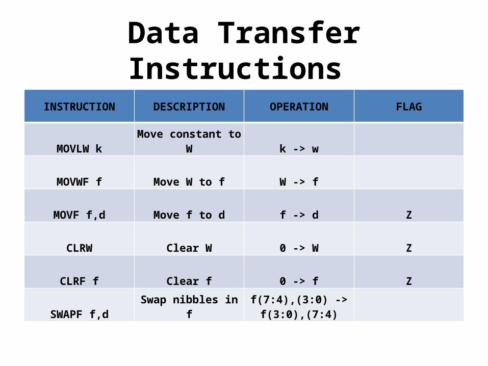
Data Transfer Instructions
INSTRUCTION DESCRIPTION OPERATION FLAG
MOVLW kMove constant to
W k -> w
MOVWF f Move W to f W -> f
MOVF f,d Move f to d f -> d Z
CLRW Clear W 0 -> W Z
CLRF f Clear f 0 -> f Z
SWAPF f,d Swap nibbles in ff(7:4),(3:0) ->
f(3:0),(7:4)

Arithmetic-logic Instructions
INSTRUCTION DESCRIPTION OPERATION FLAG
ADDLW kAdd W and constant W+k -> W C, DC, Z
ADDWF f,d Add W and f W+f -> d C, DC ,Z
SUBLW kSubtract W from constant k-W -> W C, DC, Z
SUBWF f,dSubtract W from f f-W -> d C, DC, Z
ANDLW kLogical AND with W with constant W AND k -> W Z
ANDWF f,dLogical AND with W with f W AND f -> d Z
ANDWF f,dLogical AND with W with f W AND f -> d Z
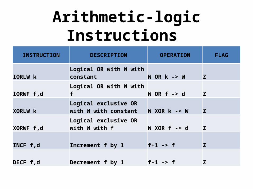
Arithmetic-logic Instructions
INSTRUCTION DESCRIPTION OPERATION FLAG
IORLW kLogical OR with W with constant W OR k -> W Z
IORWF f,dLogical OR with W with f W OR f -> d Z
XORLW kLogical exclusive OR with W with constant W XOR k -> W Z
XORWF f,dLogical exclusive OR with W with f W XOR f -> d Z
INCF f,d Increment f by 1 f+1 -> f Z
DECF f,d Decrement f by 1 f-1 -> f Z
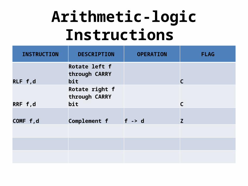
Arithmetic-logic Instructions
INSTRUCTION DESCRIPTION OPERATION FLAG
RLF f,d
Rotate left f through CARRY bit C
RRF f,d
Rotate right f through CARRY bit C
COMF f,d Complement f f -> d Z
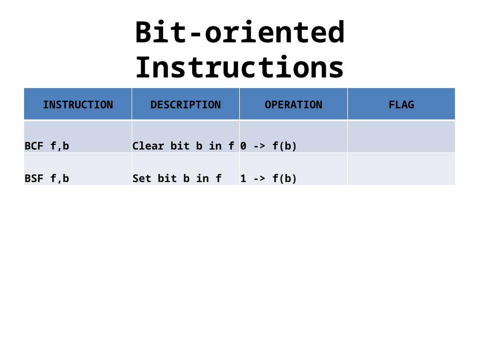
Bit-oriented Instructions
INSTRUCTION DESCRIPTION OPERATION FLAG
BCF f,b Clear bit b in f 0 -> f(b)
BSF f,b Set bit b in f 1 -> f(b)
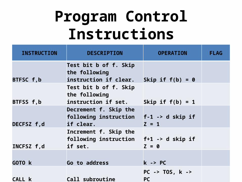
Program Control Instructions
INSTRUCTION DESCRIPTION OPERATION FLAG
BTFSC f,b
Test bit b of f. Skip the following instruction if clear. Skip if f(b) = 0
BTFSS f,b
Test bit b of f. Skip the following instruction if set. Skip if f(b) = 1
DECFSZ f,d
Decrement f. Skip the following instruction if clear.
f-1 -> d skip if Z = 1
INCFSZ f,d
Increment f. Skip the following instruction if set.
f+1 -> d skip if Z = 0
GOTO k Go to address k -> PC
CALL k Call subroutine PC -> TOS, k -> PC
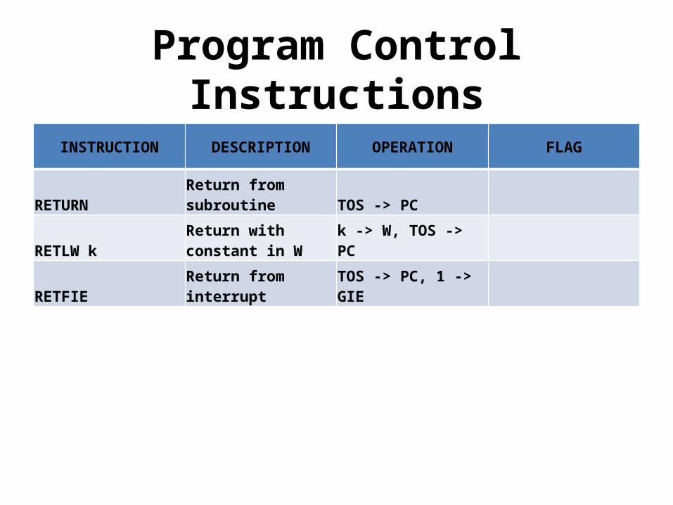
Program Control Instructions
INSTRUCTION DESCRIPTION OPERATION FLAG
RETURNReturn from subroutine TOS -> PC
RETLW kReturn with constant in W k -> W, TOS -> PC
RETFIEReturn from interrupt
TOS -> PC, 1 -> GIE

Other instructions
INSTRUCTION DESCRIPTION OPERATION FLAG
NOP No operationTOS -> PC, 1 -> GIE
CLRWDTClear watchdog timer
0 -> WDT, 1 -> TO, 1 -> PD TO, PD
SLEEPGo into sleep mode
0 -> WDT, 1 -> TO, 0 -> PD TO, PD
33TMT H E A R C H I T E C T U R E F O R T H E D I G I T A L W O R L D
The ARM Architecture
34TM 3439v10 The ARM Architecture
Agenda
Introduction to ARM Ltd
Programmers Model
Instruction Set
System Design
Development Tools
35TM 3539v10 The ARM Architecture
ARM Ltd
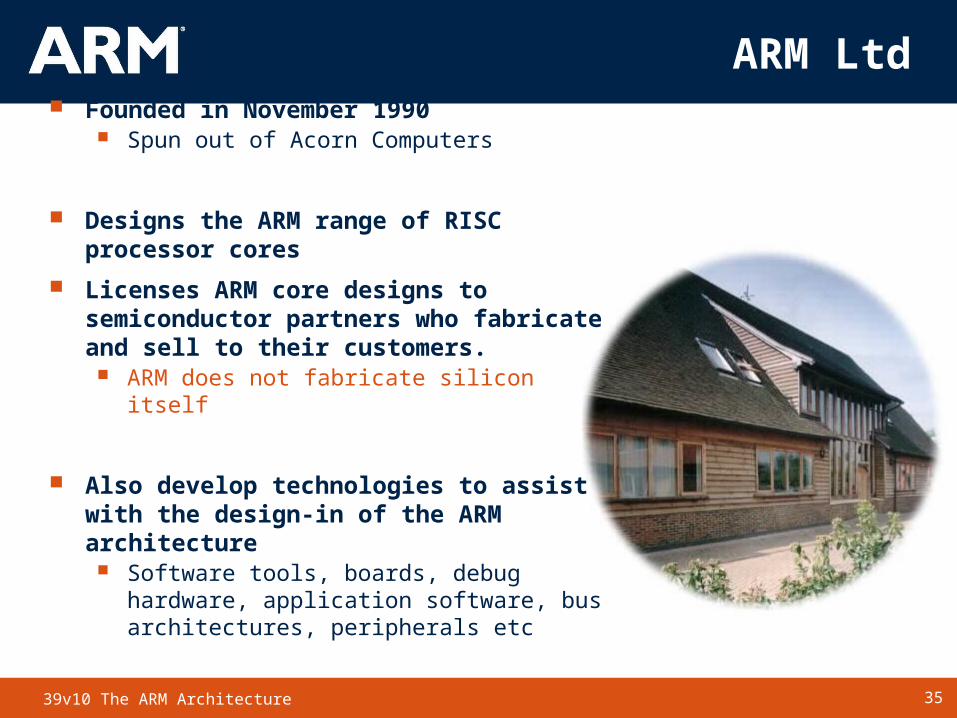
Founded in November 1990 Spun out of Acorn Computers
Designs the ARM range of RISC processor cores
Licenses ARM core designs to semiconductor partners who fabricate and sell to their customers.
ARM does not fabricate silicon itself
Also develop technologies to assist with the design-in of the ARM architecture
Software tools, boards, debug hardware, application software, bus architectures, peripherals etc
36TM 3639v10 The ARM Architecture
Agenda
Introduction to ARM Ltd
Programmers Model
Instruction Sets
System Design
Development Tools
37TM 3739v10 The ARM Architecture
Data Sizes and Instruction Sets
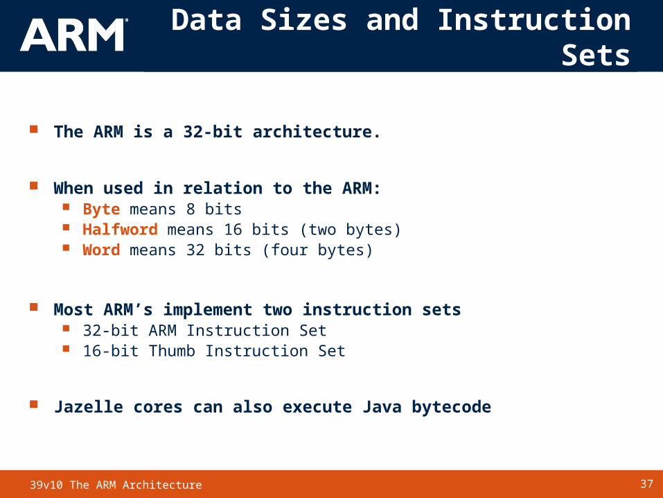
The ARM is a 32-bit architecture.
When used in relation to the ARM: Byte means 8 bits Halfword means 16 bits (two bytes) Word means 32 bits (four bytes)
Most ARM’s implement two instruction sets 32-bit ARM Instruction Set 16-bit Thumb Instruction Set
Jazelle cores can also execute Java bytecode
38TM 3839v10 The ARM Architecture
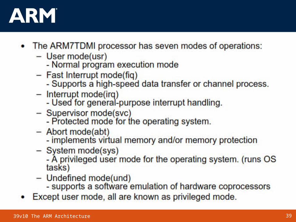
Processor Modes
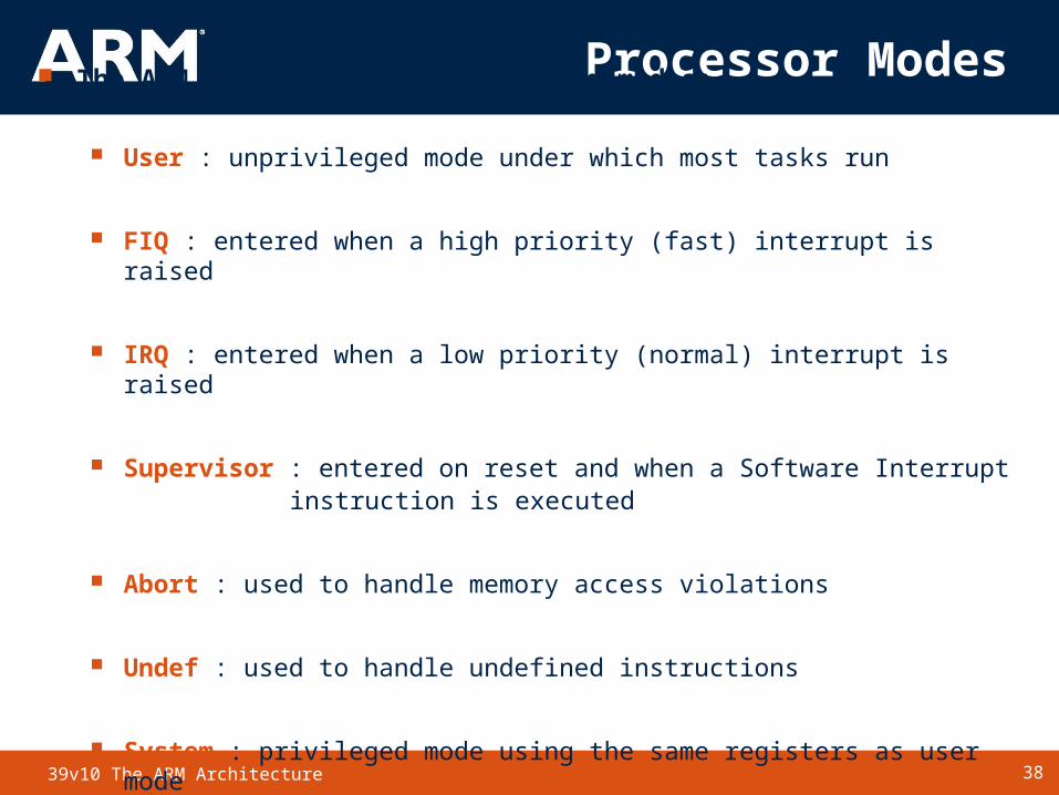
The ARM has seven basic operating modes:
User : unprivileged mode under which most tasks run
FIQ : entered when a high priority (fast) interrupt is raised
IRQ : entered when a low priority (normal) interrupt is raised
Supervisor : entered on reset and when a Software Interrupt instruction is executed
Abort : used to handle memory access violations
Undef : used to handle undefined instructions
System : privileged mode using the same registers as user mode
39TM 3939v10 The ARM Architecture
40TM 4039v10 The ARM Architecture
r0
r1
r2
r3
r4
r5
r6
r7
r8
r9
r10
r11
r12
r13 (sp)
r14 (lr)
r15 (pc)
cpsr
r13 (sp)
r14 (lr)
spsr
r13 (sp)
r14 (lr)
spsr
r13 (sp)
r14 (lr)
spsr
r13 (sp)
r14 (lr)
spsr
r8
r9
r10
r11
r12
r13 (sp)
r14 (lr)
spsr
FIQ IRQ SVC Undef Abort
User Moder0
r1
r2
r3
r4
r5
r6
r7
r8
r9
r10
r11
r12
r13 (sp)
r14 (lr)
r15 (pc)
cpsr
r13 (sp)
r14 (lr)
spsr
r13 (sp)
r14 (lr)
spsr
r13 (sp)
r14 (lr)
spsr
r13 (sp)
r14 (lr)
spsr
r8
r9
r10
r11
r12
r13 (sp)
r14 (lr)
spsr
Current Visible Registers
Banked out Registers
FIQ IRQ SVC Undef Abort
r0
r1
r2
r3
r4
r5
r6
r7
r15 (pc)
cpsr
r13 (sp)
r14 (lr)
spsr
r13 (sp)
r14 (lr)
spsr
r13 (sp)
r14 (lr)
spsr
r13 (sp)
r14 (lr)
spsr
r8
r9
r10
r11
r12
r13 (sp)
r14 (lr)
spsr
Current Visible Registers
Banked out Registers
User IRQ SVC Undef Abort
r8
r9
r10
r11
r12
r13 (sp)
r14 (lr)
FIQ ModeIRQ Moder0
r1
r2
r3
r4
r5
r6
r7
r8
r9
r10
r11
r12
r15 (pc)
cpsr
r13 (sp)
r14 (lr)
spsr
r13 (sp)
r14 (lr)
spsr
r13 (sp)
r14 (lr)
spsr
r13 (sp)
r14 (lr)
spsr
r8
r9
r10
r11
r12
r13 (sp)
r14 (lr)
spsr
Current Visible Registers
Banked out Registers
User FIQ SVC Undef Abort
r13 (sp)
r14 (lr)
Undef Moder0
r1
r2
r3
r4
r5
r6
r7
r8
r9
r10
r11
r12
r15 (pc)
cpsr
r13 (sp)
r14 (lr)
spsr
r13 (sp)
r14 (lr)
spsr
r13 (sp)
r14 (lr)
spsr
r13 (sp)
r14 (lr)
spsr
r8
r9
r10
r11
r12
r13 (sp)
r14 (lr)
spsr
Current Visible Registers
Banked out Registers
User FIQ IRQ SVC Abort
r13 (sp)
r14 (lr)
SVC Moder0
r1
r2
r3
r4
r5
r6
r7
r8
r9
r10
r11
r12
r15 (pc)
cpsr
r13 (sp)
r14 (lr)
spsr
r13 (sp)
r14 (lr)
spsr
r13 (sp)
r14 (lr)
spsr
r13 (sp)
r14 (lr)
spsr
r8
r9
r10
r11
r12
r13 (sp)
r14 (lr)
spsr
Current Visible Registers
Banked out Registers
User FIQ IRQ Undef Abort
r13 (sp)
r14 (lr)
Abort Mode r0
r1
r2
r3
r4
r5
r6
r7
r8
r9
r10
r11
r12
r15 (pc)
cpsr
r13 (sp)
r14 (lr)
spsr
r13 (sp)
r14 (lr)
spsr
r13 (sp)
r14 (lr)
spsr
r13 (sp)
r14 (lr)
spsr
r8
r9
r10
r11
r12
r13 (sp)
r14 (lr)
spsr
Current Visible Registers
Banked out Registers
User FIQ IRQ SVC Undef
r13 (sp)
r14 (lr)
The ARM Register Set
41TM 4139v10 The ARM Architecture
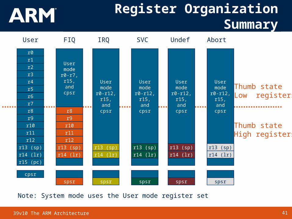
Register Organization Summary
Usermoder0-r7,r15,andcpsr
r8
r9
r10
r11
r12
r13 (sp)
r14 (lr)
spsr
FIQ
r8
r9
r10
r11
r12
r13 (sp)
r14 (lr)
r15 (pc)
cpsr
r0
r1
r2
r3
r4
r5
r6
r7
User
r13 (sp)
r14 (lr)
spsr
IRQ
Usermoder0-r12,
r15,andcpsr
r13 (sp)
r14 (lr)
spsr
Undef
Usermoder0-r12,
r15,andcpsr
r13 (sp)
r14 (lr)
spsr
SVC
Usermoder0-r12,
r15,andcpsr
r13 (sp)
r14 (lr)
spsr
Abort
Usermoder0-r12,
r15,andcpsr
Thumb stateLow registers
Thumb stateHigh registers
Note: System mode uses the User mode register set
42TM 4239v10 The ARM Architecture
The Registers
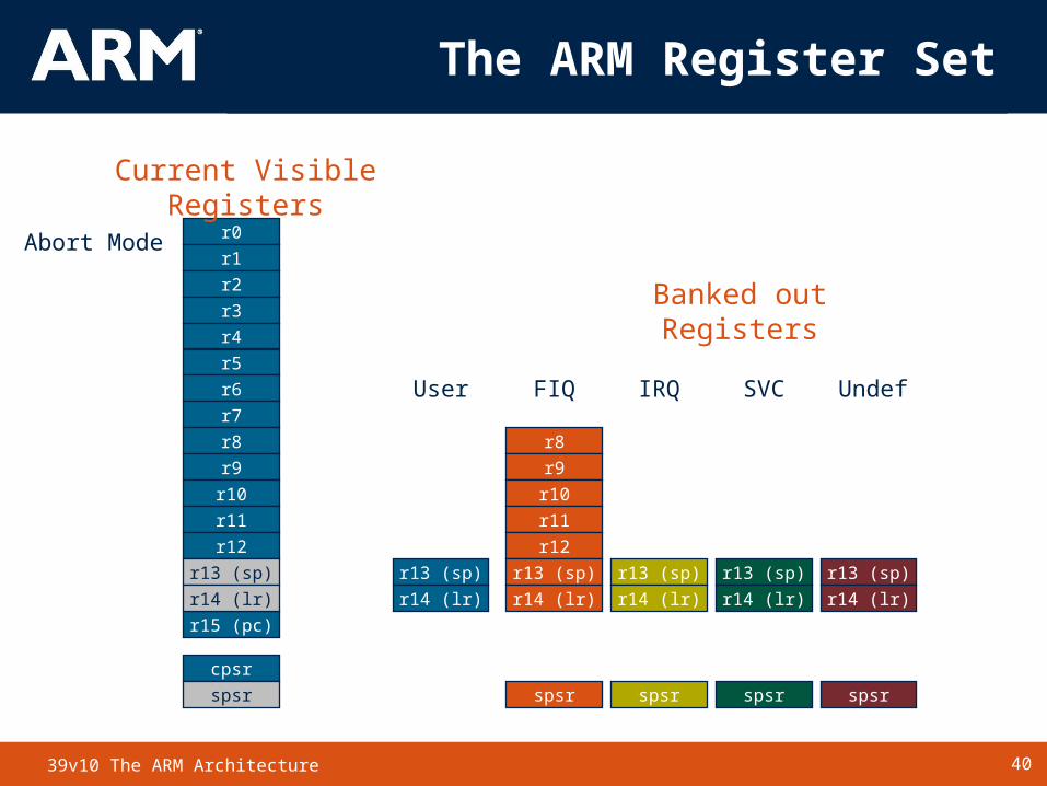
ARM has 37 registers all of which are 32-bits long. 1 dedicated program counter 1 dedicated current program status register 5 dedicated saved program status registers 30 general purpose registers
The current processor mode governs which of several banks is accessible. Each mode can access
a particular set of r0-r12 registers a particular r13 (the stack pointer, sp) and r14 (the link register, lr) the program counter, r15 (pc) the current program status register, cpsr
Privileged modes (except System) can also access a particular spsr (saved program status register)
43TM 4339v10 The ARM Architecture
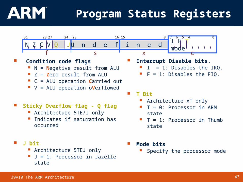
Program Status Registers
Condition code flags N = Negative result from ALU Z = Zero result from ALU C = ALU operation Carried out V = ALU operation oVerflowed
Sticky Overflow flag - Q flag Architecture 5TE/J only Indicates if saturation has occurred
J bit Architecture 5TEJ only J = 1: Processor in Jazelle state
Interrupt Disable bits. I = 1: Disables the IRQ. F = 1: Disables the FIQ.
T Bit Architecture xT only T = 0: Processor in ARM state T = 1: Processor in Thumb state
Mode bits Specify the processor mode
2731
N Z C V Q28 67
I F T mode1623
815
5 4 024
f s x c U n d e f i n e dJ
44TM 4439v10 The ARM Architecture
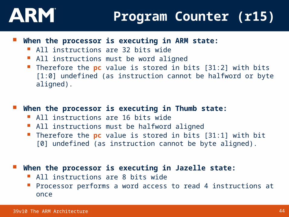
When the processor is executing in ARM state: All instructions are 32 bits wide All instructions must be word aligned Therefore the pc value is stored in bits [31:2] with bits [1:0] undefined (as
instruction cannot be halfword or byte aligned).
When the processor is executing in Thumb state: All instructions are 16 bits wide All instructions must be halfword aligned Therefore the pc value is stored in bits [31:1] with bit [0] undefined (as
instruction cannot be byte aligned).
When the processor is executing in Jazelle state: All instructions are 8 bits wide Processor performs a word access to read 4 instructions at once
Program Counter (r15)
45TM 4539v10 The ARM Architecture
Agenda
Introduction to ARM Ltd
Programmers Model
Instruction Sets
System Design
Development Tools
46TM 4639v10 The ARM Architecture
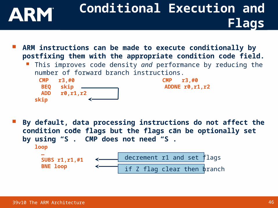
ARM instructions can be made to execute conditionally by postfixing them with the appropriate condition code field.
This improves code density and performance by reducing the number of forward branch instructions.
CMP r3,#0 CMP r3,#0 BEQ skip ADDNE r0,r1,r2 ADD r0,r1,r2skip
By default, data processing instructions do not affect the condition code flags but the flags can be optionally set by using “S”. CMP does not need “S”.
loop … SUBS r1,r1,#1 BNE loop if Z flag clear then branch
decrement r1 and set flags
Conditional Execution and Flags
47TM 4739v10 The ARM Architecture
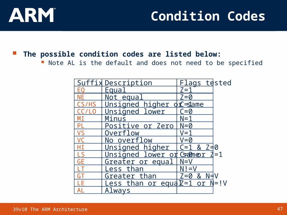
Condition Codes
Not equalUnsigned higher or sameUnsigned lowerMinus
Equal
OverflowNo overflowUnsigned higherUnsigned lower or same
Positive or Zero
Less thanGreater thanLess than or equalAlways
Greater or equal
EQNECS/HSCC/LO
PLVS
HILSGELTGTLEAL
MI
VC
Suffix Description
Z=0C=1C=0
Z=1Flags tested
N=1N=0V=1V=0C=1 & Z=0C=0 or Z=1N=VN!=VZ=0 & N=VZ=1 or N=!V
The possible condition codes are listed below: Note AL is the default and does not need to be specified
48TM 4839v10 The ARM Architecture
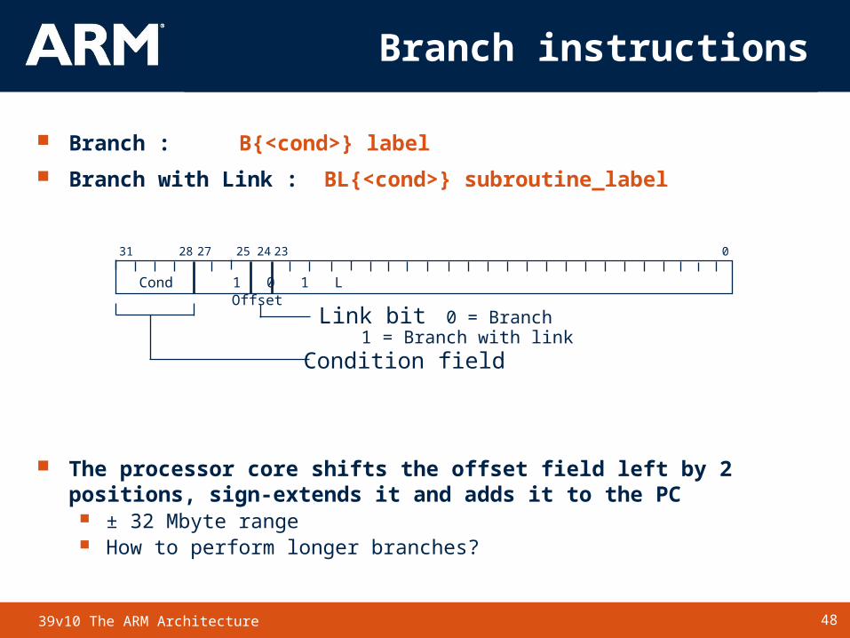
Branch : B{<cond>} label
Branch with Link : BL{<cond>} subroutine_label
The processor core shifts the offset field left by 2 positions, sign-extends it and adds it to the PC
± 32 Mbyte range How to perform longer branches?
2831 24 0
Cond 1 0 1 L Offset
Condition field
Link bit 0 = Branch1 = Branch with link
232527
Branch instructions
49TM 4939v10 The ARM Architecture
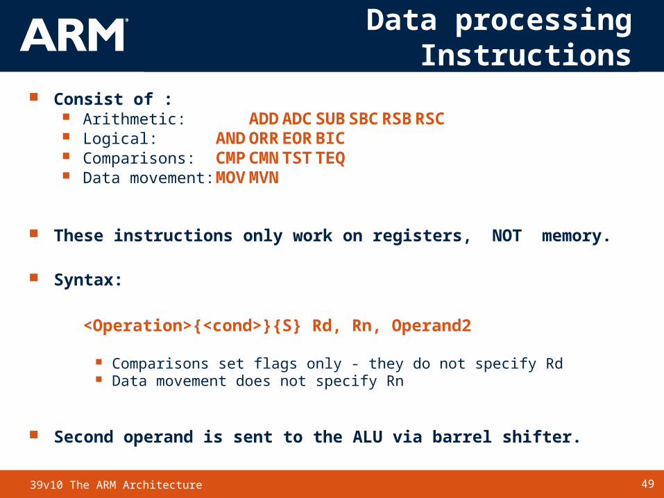
Data processing Instructions
Consist of : Arithmetic: ADD ADC SUB SBC RSB
RSC Logical: AND ORR EOR BIC Comparisons: CMP CMN TST TEQ Data movement: MOV MVN
These instructions only work on registers, NOT memory.
Syntax:
<Operation>{<cond>}{S} Rd, Rn, Operand2
Comparisons set flags only - they do not specify Rd Data movement does not specify Rn
Second operand is sent to the ALU via barrel shifter.
50TM 5039v10 The ARM Architecture
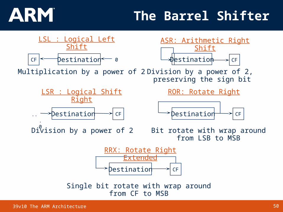
The Barrel Shifter
DestinationCF 0 Destination CF
LSL : Logical Left Shift ASR: Arithmetic Right Shift
Multiplication by a power of 2 Division by a power of 2, preserving the sign bit
Destination CF...0 Destination CF
LSR : Logical Shift Right ROR: Rotate Right
Division by a power of 2 Bit rotate with wrap aroundfrom LSB to MSB
Destination
RRX: Rotate Right Extended
Single bit rotate with wrap aroundfrom CF to MSB
CF
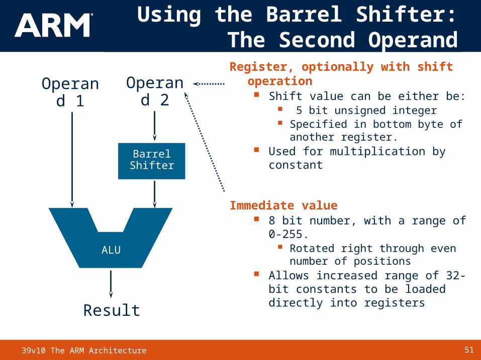
51TM 5139v10 The ARM Architecture
Register, optionally with shift operation Shift value can be either be:
5 bit unsigned integer Specified in bottom byte of another
register. Used for multiplication by constant
Immediate value 8 bit number, with a range of 0-255.
Rotated right through even number of positions
Allows increased range of 32-bit constants to be loaded directly into registers
Result
Operand 1
BarrelShifter
Operand 2
ALU
Using the Barrel Shifter:The Second Operand
52TM 5239v10 The ARM Architecture
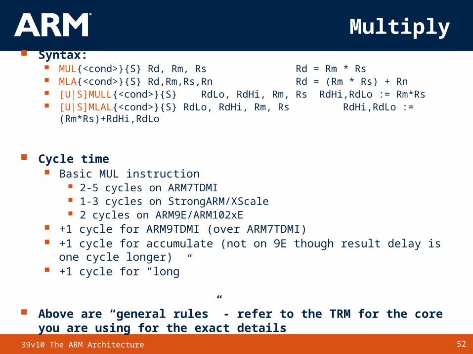
Multiply
Syntax: MUL{<cond>}{S} Rd, Rm, Rs Rd = Rm * Rs MLA{<cond>}{S} Rd,Rm,Rs,Rn Rd = (Rm * Rs) + Rn [U|S]MULL{<cond>}{S} RdLo, RdHi, Rm, Rs RdHi,RdLo := Rm*Rs [U|S]MLAL{<cond>}{S} RdLo, RdHi, Rm, Rs RdHi,RdLo := (Rm*Rs)
+RdHi,RdLo
Cycle time Basic MUL instruction
2-5 cycles on ARM7TDMI 1-3 cycles on StrongARM/XScale 2 cycles on ARM9E/ARM102xE
+1 cycle for ARM9TDMI (over ARM7TDMI) +1 cycle for accumulate (not on 9E though result delay is one cycle longer) +1 cycle for “long”
Above are “general rules” - refer to the TRM for the core you are using for the exact details
53TM 5339v10 The ARM Architecture
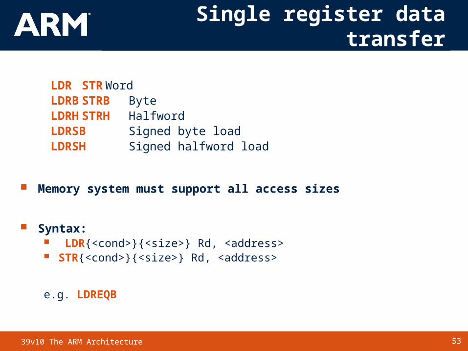
Single register data transfer
LDR STR Word LDRB STRB Byte LDRH STRH Halfword LDRSB Signed byte load LDRSH Signed halfword load
Memory system must support all access sizes
Syntax: LDR{<cond>}{<size>} Rd, <address> STR{<cond>}{<size>} Rd, <address>
e.g. LDREQB
54TM 5439v10 The ARM Architecture
Address accessed
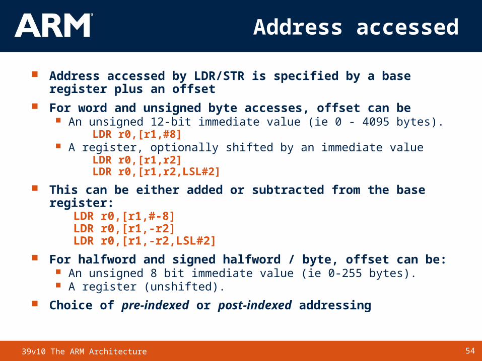
Address accessed by LDR/STR is specified by a base register plus an offset
For word and unsigned byte accesses, offset can be An unsigned 12-bit immediate value (ie 0 - 4095 bytes).
LDR r0,[r1,#8] A register, optionally shifted by an immediate value
LDR r0,[r1,r2]LDR r0,[r1,r2,LSL#2]
This can be either added or subtracted from the base register:LDR r0,[r1,#-8]LDR r0,[r1,-r2]LDR r0,[r1,-r2,LSL#2]
For halfword and signed halfword / byte, offset can be: An unsigned 8 bit immediate value (ie 0-255 bytes). A register (unshifted).
Choice of pre-indexed or post-indexed addressing
55TM 5539v10 The ARM Architecture
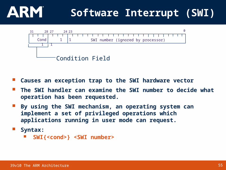
Software Interrupt (SWI)
Causes an exception trap to the SWI hardware vector
The SWI handler can examine the SWI number to decide what operation has been requested.
By using the SWI mechanism, an operating system can implement a set of privileged operations which applications running in user mode can request.
Syntax: SWI{<cond>} <SWI number>
2831 2427 0
Cond 1 1 1 1 SWI number (ignored by processor)
23
Condition Field
56TM 5639v10 The ARM Architecture
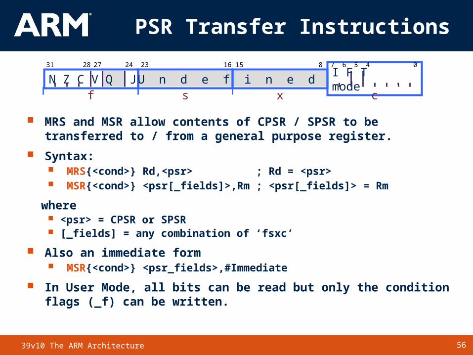
PSR Transfer Instructions
MRS and MSR allow contents of CPSR / SPSR to be transferred to / from a general purpose register.
Syntax: MRS{<cond>} Rd,<psr> ; Rd = <psr> MSR{<cond>} <psr[_fields]>,Rm ; <psr[_fields]> = Rm
where <psr> = CPSR or SPSR [_fields] = any combination of ‘fsxc’
Also an immediate form MSR{<cond>} <psr_fields>,#Immediate
In User Mode, all bits can be read but only the condition flags (_f) can be written.
2731
N Z C V Q28 67
I F T mode1623
815
5 4 024
f s x c U n d e f i n e dJ
57TM 5739v10 The ARM Architecture
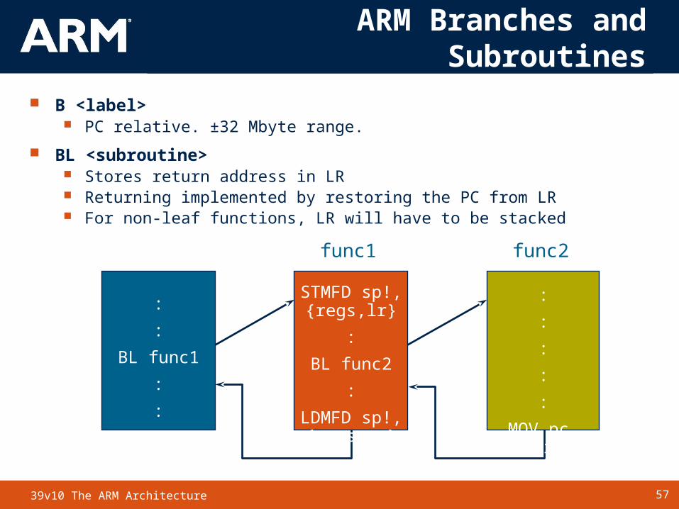
ARM Branches and Subroutines
B <label> PC relative. ±32 Mbyte range.
BL <subroutine> Stores return address in LR Returning implemented by restoring the PC from LR For non-leaf functions, LR will have to be stacked
STMFD sp!,{regs,lr}
:
BL func2
:
LDMFD sp!,{regs,pc}
func1 func2
:
:
BL func1
:
:
:
:
:
:
:
MOV pc, lr