4 mbit rom + 1 mbit / 256 kbit sram rom/ram combo 1. a write occurs during the overlap (twp) of a...
TRANSCRIPT

Data Sheet
FEATURES:
• ROM + SRAM ROM/RAM Combo– SST30VR041: 512K x8 ROM + 128K x8 SRAM– SST30VR043: 512K x8 ROM + 32K x8 SRAM
• ROM/RAM combo on a monolithic chip• Equivalent ComboMemory (Flash + SRAM):
SST31LF041A for code development andpre-production
• Wide Operating Voltage Range: 2.7-3.3V• Chip Access Time
– SST30VR041 70 ns and 150 ns– SST30VR043 150 ns
• Low Power Dissipation:– Standby: 1.0 µW (Typical)– Operating: 3.0 mW (Typical)
• Fully Static Operation– No clock or refresh required
• Three-state Outputs• Packages Available
– 32-lead TSOP (8mm x14mm)
4 Mbit ROM + 1 Mbit / 256 Kbit SRAMROM/RAM Combo
SST30VR041 / SST30VR043SST30VR041 / 0434Mb Mask ROM (x8) + 1Mb / 256Kb SRAM (x8) Combo
PRODUCT DESCRIPTION
The SST30VR041/043 are ROM/RAM combo chipsconsisting of 4 Mbit Read-Only Memory (ROM) orga-nized as 512 KByte and a Static Random AccessMemory (SRAM) organized as either 128 or 32 KByte.Output Enable Input (OE#) is pin-shared withRAMCS# (RAM Enable Input) signal in order to main-tain the standard 32-lead TSOP package.
The device is fabricated using SST’s advanced CMOS lowpower process technology.
The SST30VR041/043 have an output enable input for pre-cise control of the data outputs. It also has two (2) separatechip enable inputs for selection of either SRAM or ROMand for minimizing current drain during power-down mode.
The SST30VR041/043 is particularly well suited for use inlow voltage (2.7-3.3V) supplies such as pagers, organizersand other handheld applications.
RAMCS#
OE#/RAMCS#
ROMCS#
WE#
AMS-A0
Note: AMS = Most Significant Address
DQ7-DQ0
ROMCS#
RAM
ROM
WE#OE#
OE#
381 ILL B1.2
Con
trol
Circ
uit
Add
ress
Buf
fer
Dat
a B
uffe
r
FUNCTIONAL BLOCK DIAGRAM
©2002 Silicon Storage Technology, Inc.S71134-02-000 2/02 3811
The SST logo and SuperFlash are registered trademarks of Silicon Storage Technology, Inc.ComboMemory is a trademark of Silicon Storage Technology, Inc.
These specifications are subject to change without notice.

Data Sheet
4 Mbit ROM + 1 Mbit / 256 Kbit SRAM ROM/RAM ComboSST30VR041 / SST30VR043
FIGURE 1: PIN ASSIGNMENTS FOR 32-LEAD TSOP
TABLE 1: PIN DESCRIPTION
Symbol Pin Name
AMS1-A0
1. AMS = Most significant address
Address Inputs:
ROM: AMS = A18
RAM: AMS = A16 for SST30VR041A14 for SST30VR043
WE# Write Enable Input
OE#/RAMCS# Output Enable/RAM Enable Input
ROMCS# ROM Enable Input
DQ7-DQ0 Data Input/Output
VDD Power Supply
VSS GroundT1.3 381
A11A9A8
A13A14A17
WE#VDDA18A16A15A12
A7A6A5A4
12345678910111213141516
OE#/RAMCS#A10ROMCS#DQ7DQ6DQ5DQ4DQ3VSSDQ2DQ1DQ0A0A1A2A3
32313029282726252423222120191817
381 ILL F01.0
Standard Pinout
Top View
Die Up
2©2002 Silicon Storage Technology, Inc. S71134-02-000 2/02 381

Data Sheet
4 Mbit ROM + 1 Mbit / 256 Kbit SRAM ROM/RAM ComboSST30VR041 / SST30VR043
Absolute Maximum Stress Ratings (Applied conditions greater than those listed under “Absolute MaximumStress Ratings” may cause permanent damage to the device. This is a stress rating only and functional operationof the device at these conditions or conditions greater than those defined in the operational sections of this datasheet is not implied. Exposure to absolute maximum stress rating conditions may affect device reliability.)
Operating Temperature . . . . . . . . . . . . . . . . . . . . . . . . . . . . . . . . . . . . . . . . . . . . . . . . . . . . . . . . . . . -20°C to +85°CStorage Temperature . . . . . . . . . . . . . . . . . . . . . . . . . . . . . . . . . . . . . . . . . . . . . . . . . . . . . . . . . . . -65°C to +150°CVoltage on Any Pin Relative to VSS . . . . . . . . . . . . . . . . . . . . . . . . . . . . . . . . . . . . . . . . . . . . . . . . -0.5V to VDD+0.5VVoltage on VDD Supply Relative to VSS . . . . . . . . . . . . . . . . . . . . . . . . . . . . . . . . . . . . . . . . . . . . . . . . . -0.5V to 4.0VPower Dissipation. . . . . . . . . . . . . . . . . . . . . . . . . . . . . . . . . . . . . . . . . . . . . . . . . . . . . . . . . . . . . . . . . . . . . . . . 1.0WSoldering Temperature (10 Seconds Lead Only) . . . . . . . . . . . . . . . . . . . . . . . . . . . . . . . . . . . . . . . . . . . . . . 260°C
OPERATING RANGE
Range Ambient Temp VDD
Commercial 0°C to +70°C 2.7-3.3V
Extended -20°C to +85°C 2.7-3.3V
AC CONDITIONS OF TEST
Input Pulse Level . . . . . . . . . . . . . . . . . . . . 0-VDD
Input & Output Timing Reference Levels . . . VDD/2
Input Rise/Fall Time . . . . . . . . . . . . . . . . . . . 5 ns
Output Load . . . . . . . . . . . . . . . . . . . . . . . . . CL = 30 pF for 70 ns
Output Load . . . . . . . . . . . . . . . . . . . . . . . . . CL = 100 pF for 150 ns
3©2002 Silicon Storage Technology, Inc. S71134-02-000 2/02 381

Data Sheet
4 Mbit ROM + 1 Mbit / 256 Kbit SRAM ROM/RAM ComboSST30VR041 / SST30VR043
TABLE 2: RECOMMENDED DC OPERATING CONDITIONS
Symbol Parameter Min Max Units
VDD Supply Voltage 2.7 3.3 V
VSS Ground 0 0 V
VIH Input High Voltage 2.4 VDD + 0.5 V
VIL Input Low Voltage -0.3 0.3 VT2.0 381
TABLE 3: DC OPERATING CHARACTERISTICS
Symbol Parameter
VDD = 2.7-3.3V
Test ConditionsMin Max Units
IDD1 ROM Operating Supply Current 4.0+1.1(f)1
1. f = Frequency of operation (MHz) = 1/cycle time
mA ROMCS#=VIL, RAMCS#=VIH,VIN=VIH or VIL, II/O=Opens
IDD2 SRAM Operating Supply Current 2.5+1(f)1 mA ROMCS#=VIH, RAMCS#=VIL, II/O=Opens
ISB Standby VDD Current 10 µA ROMCS# ≥ VDD-0.2V, RAMCS# ≥ VDD-0.2VVIN ≥ VDD-0.2V or VIN ≤ 0.2V
ILI Input Leakage Current -1 1 µA VIN=VSS to VDD
ILO Output Leakage Current -1 1 µA ROMCS#=RAMCS#=VIH or OE#=VIH orWE#=VIL, VI/O=VSS to VDD
VOL Output Low Voltage 0.4 V IOL=1.0 mA
VOH Output High Voltage 2.2 V IOH=-0.5 mAT3.5 381
TABLE 4: CAPACITANCE (Ta = 25°C, f=1 Mhz)
Parameter Description Test Condition Maximum
CI/O1
1. This parameter is measured only for initial qualification and after a design or process change that could affect this parameter.
I/O Pin Capacitance VI/O = 0V 8 pF
CIN1 Input Capacitance VIN = 0V 6 pF
T4.1 381
4©2002 Silicon Storage Technology, Inc. S71134-02-000 2/02 381

Data Sheet
4 Mbit ROM + 1 Mbit / 256 Kbit SRAM ROM/RAM ComboSST30VR041 / SST30VR043
FIGURE 2: AC INPUT/OUTPUT REFERENCE WAVEFORMS
FIGURE 3: A TEST LOAD EXAMPLE
381 ILL F07.0
REFERENCE POINTS OUTPUTINPUT VIT
VIHT
VILT
VOT
AC test inputs are driven at VIHT (0.9 VDD) for a logic “1” and VILT (0.1 VDD) for a logic “0”. Measurement reference pointsfor inputs and outputs are VIT (0.5 VDD) and VOT (0.5 VDD). Input rise and fall times (10% ↔ 90%) are <5 ns.
Note: VIT - VINPUT TestVOT - VOUTPUT TestVIHT - VINPUT HIGH TestVILT - VINPUT LOW Test
381 ILL F08.0
TO TESTER
TO DUT
CL
5©2002 Silicon Storage Technology, Inc. S71134-02-000 2/02 381
Data Sheet
4 Mbit ROM + 1 Mbit / 256 Kbit SRAM ROM/RAM ComboSST30VR041 / SST30VR043
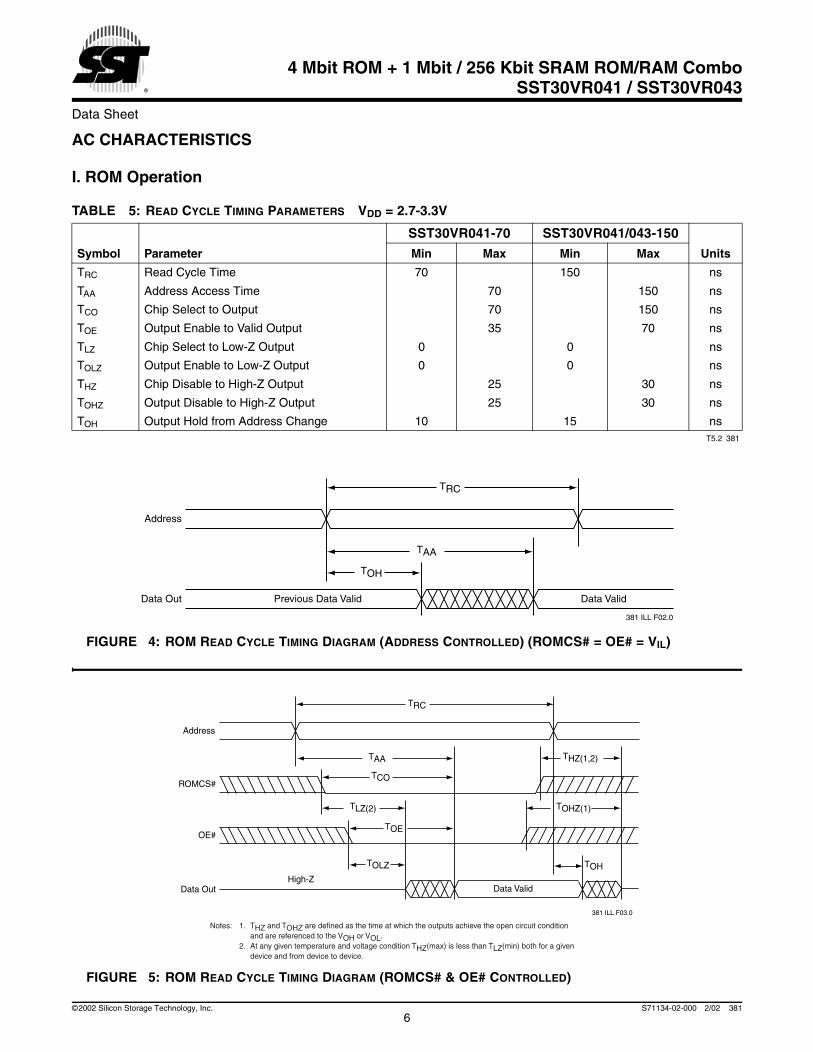
AC CHARACTERISTICS
I. ROM Operation
FIGURE 4: ROM READ CYCLE TIMING DIAGRAM (ADDRESS CONTROLLED) (ROMCS# = OE# = VIL)
FIGURE 5: ROM READ CYCLE TIMING DIAGRAM (ROMCS# & OE# CONTROLLED)
TABLE 5: READ CYCLE TIMING PARAMETERS VDD = 2.7-3.3V
Symbol Parameter
SST30VR041-70 SST30VR041/043-150
UnitsMin Max Min Max
TRC Read Cycle Time 70 150 ns
TAA Address Access Time 70 150 ns
TCO Chip Select to Output 70 150 ns
TOE Output Enable to Valid Output 35 70 ns
TLZ Chip Select to Low-Z Output 0 0 ns
TOLZ Output Enable to Low-Z Output 0 0 ns
THZ Chip Disable to High-Z Output 25 30 ns
TOHZ Output Disable to High-Z Output 25 30 ns
TOH Output Hold from Address Change 10 15 nsT5.2 381
TRC
TAA
Data Valid
381 ILL F02.0
Data Out Previous Data Valid
Address
TOH
TRC
TAA
TCO
TLZ(2) TOHZ(1)
TOH
THZ(1,2)
Data Valid
381 ILL F03.0
Data Out
OE#
ROMCS#
High-Z
Address
TOE
TOLZ
Notes: 1. THZ and TOHZ are defined as the time at which the outputs achieve the open circuit condition and are referenced to the VOH or VOL.
2. At any given temperature and voltage condition THZ(max) is less than TLZ(min) both for a given device and from device to device.
6©2002 Silicon Storage Technology, Inc. S71134-02-000 2/02 381
Data Sheet
4 Mbit ROM + 1 Mbit / 256 Kbit SRAM ROM/RAM ComboSST30VR041 / SST30VR043
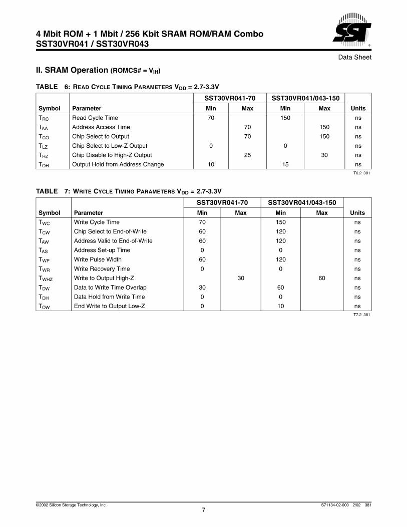
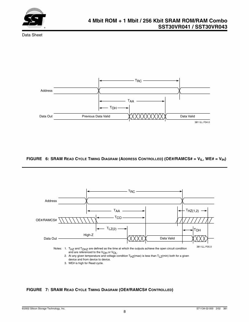
II. SRAM Operation (ROMCS# = VIH)
TABLE 6: READ CYCLE TIMING PARAMETERS VDD = 2.7-3.3V
Symbol Parameter
SST30VR041-70 SST30VR041/043-150
UnitsMin Max Min Max
TRC Read Cycle Time 70 150 ns
TAA Address Access Time 70 150 ns
TCO Chip Select to Output 70 150 ns
TLZ Chip Select to Low-Z Output 0 0 ns
THZ Chip Disable to High-Z Output 25 30 ns
TOH Output Hold from Address Change 10 15 nsT6.2 381
TABLE 7: WRITE CYCLE TIMING PARAMETERS VDD = 2.7-3.3V
Symbol Parameter
SST30VR041-70 SST30VR041/043-150
UnitsMin Max Min Max
TWC Write Cycle Time 70 150 ns
TCW Chip Select to End-of-Write 60 120 ns
TAW Address Valid to End-of-Write 60 120 ns
TAS Address Set-up Time 0 0 ns
TWP Write Pulse Width 60 120 ns
TWR Write Recovery Time 0 0 ns
TWHZ Write to Output High-Z 30 60 ns
TDW Data to Write Time Overlap 30 60 ns
TDH Data Hold from Write Time 0 0 ns
TOW End Write to Output Low-Z 0 10 nsT7.2 381
7©2002 Silicon Storage Technology, Inc. S71134-02-000 2/02 381
Data Sheet
4 Mbit ROM + 1 Mbit / 256 Kbit SRAM ROM/RAM ComboSST30VR041 / SST30VR043
FIGURE 6: SRAM READ CYCLE TIMING DIAGRAM (ADDRESS CONTROLLED) (OE#/RAMCS# = VIL, WE# = VIH)
FIGURE 7: SRAM READ CYCLE TIMING DIAGRAM (OE#/RAMCS# CONTROLLED)
TRC
TAA
Data Valid
381 ILL F04.0
Data Out Previous Data Valid
Address
TOH
TRC
TAA
TCO
TLZ(2) TOH
THZ(1,2)
Data Valid
381 ILL F05.0
Data Out
OE#/RAMCS#
High-Z
Address
Notes: 1. THZ and TOHZ are defined as the time at which the outputs achieve the open circuit condition and are referenced to the VOH or VOL.
2. At any given temperature and voltage condition THZ(max) is less than TLZ(min) both for a given device and from device to device.
3. WE# is high for Read cycle.
8©2002 Silicon Storage Technology, Inc. S71134-02-000 2/02 381

Data Sheet
4 Mbit ROM + 1 Mbit / 256 Kbit SRAM ROM/RAM ComboSST30VR041 / SST30VR043
FIGURE 8: SRAM WRITE CYCLE TIMING DIAGRAM
TWC
TAW
TCW(2)
TOH
TDHTDW
TOW
TWR(4)
Data Valid
381 ILL F06.0
Data In
Data Out
WE#
OE#/RAMCS#
High-Z
High-Z (6)(7) (8)
Address
TWP(1)TAS(3)
TWHZ(5)
Notes: 1. A write occurs during the overlap (TWP) of a low RAMCS# and low WE#. A write begins at the latest transition among RAMCS# going low and WE# going low: A write end at the earliest transition among RAMCS# going high and WE# going high, TWP is measured from the beginning of write to the end of write.
2. TCW is measured from the later of RAMCS# going low to the end of write.3. TAS is measured from the address valid to the beginning of write.4. TWR is measured from the end of write to the address change.5. If RAMCS#, WE# are in the read mode during this period, the I/O pins are in the outputs Low-Z state.
Inputs of opposite phase of the output must not be applied because bus contention can occur.6. If RAMCS# goes low simultaneously with WE# going low or after WE# going low, the outputs remain high impedance state.7. DOUT is the same phase of the latest written data in this write cycle.8. DOUT is the read data of new address9. ROMCS# = VIH
9©2002 Silicon Storage Technology, Inc. S71134-02-000 2/02 381

Data Sheet
4 Mbit ROM + 1 Mbit / 256 Kbit SRAM ROM/RAM ComboSST30VR041 / SST30VR043
TABLE 8: FUNCTIONAL DESCRIPTION/TRUTH TABLE
Address Inputs ROMCS#OE#/RAMCS#1
(Pin 32) WE# DQ7-DQ0
X2 VIH VIH X Z Standby
AMS3-A0 VIL OE# (H) X Z Output Floating
VIL OE# (L) X DOUT ROM Read
Only AMS4-A0 are valid VIH RAMCS# (L) VIH DOUT RAM Read
VIH RAMCS# (L) VIL DIN RAM WriteT8.4 381
1. OE# & RAMCS# are pin-shared2. X can be VIL or VIH, but no other value.3. For ROM: AMS = A18 for SST30VR041 and SST30VR0434. For SRAM:AMS = A16 for SST30VR041, A18-A17 must be fixed to “VIL” or “VIH”
AMS = A14 for SST30VR043, A18-A15 must be fixed to “VIL” or “VIH”
10©2002 Silicon Storage Technology, Inc. S71134-02-000 2/02 381

Data Sheet
4 Mbit ROM + 1 Mbit / 256 Kbit SRAM ROM/RAM ComboSST30VR041 / SST30VR043
PRODUCT ORDERING INFORMATION
Valid combinations for SST30VR041
SST30VR041-70-C-WHSST30VR041-150-C-WH
SST30VR041-70-E-WHSST30VR041-150-E-WH
Valid combinations for SST30VR043
SST30VR043-150-C-WH
SST30VR043-150-E-WH
Note: Valid combinations are those products in mass production or will be in mass production. Consult your SST sales representative to confirm availability of valid combinations and to determine availability of new combinations.
Package ModifierH = 32 leads
Package TypeW = TSOP (type 1, die up, 8mm x 14mm)
Temperature RangeC = Commercial = 0°C to +70°CE = Extended = -20°C to +85°C
Read Access Speed70 = 70 ns
150 = 150 ns
Device Density041 = 4 Mbit ROM + 1 Mbit SRAM043 = 4 Mbit ROM + 256 Kbit SRAM
Voltage RangeV = 2.7-3.3V
Device Family30 = ROM/RAM
Device Speed Suffix1 Suffix2
SST30VR0xx - XXX - X - XX
11©2002 Silicon Storage Technology, Inc. S71134-02-000 2/02 381

Data Sheet
4 Mbit ROM + 1 Mbit / 256 Kbit SRAM ROM/RAM ComboSST30VR041 / SST30VR043
PACKAGING DIAGRAMS
32-LEAD THIN SMALL OUTLINE PACKAGE (TSOP) 8MM X 14MM
SST PACKAGE CODE: WH
32-tsop-WH-7
Note: 1. Complies with JEDEC publication 95 MO-142 BA dimensions,although some dimensions may be more stringent.
2. All linear dimensions are in millimeters (max/min).3. Coplanarity: 0.1 mm4. Maximum allowable mold flash is 0.15 mm at the package ends, and 0.25 mm between leads.
1.20max.
1mm
Pin # 1 Identifier
12.5012.30
14.2013.80
0.700.50
8.107.90
0.270.17
0.50BSC
1.050.95
0.150.05
0.700.50
0˚- 5˚
DETAIL
Silicon Storage Technology, Inc. • 1171 Sonora Court • Sunnyvale, CA 94086 • Telephone 408-735-9110 • Fax 408-735-9036www.SuperFlash.com or www.sst.com
12©2002 Silicon Storage Technology, Inc. S71134-02-000 2/02 381