26cdn.intechopen.com/...material...microelectronics_assembly_proces… · microelectronics assembly...
TRANSCRIPT

26
Material Characterization and Failure Analysis for
Microelectronics Assembly Processes
Chien-Yi Huang1,2, Ming-Shu Li1, Shan-Yu Huang1, Cheng-I Chang1 and Min-Hui Huang1
1Process Technology Enabling & Materials Characterization Div. Operations,
Wistron Corporation, Hsinchu 300, Taiwan, 2Department of Industrial Engineering and Management,
National Taipei University of Technology, Taipei 106, Taiwan,
R.O.C.
1. Introduction
In recent decades, the electronic industry has shown a clear trend towards miniaturization with increasing functionality. In the context of essential competition within the market, the reliability of long term operations has become a popular issue. This study examines the properties of printed circuit board (PCB) and its failure phenomena. PCB reliability is characterized through verifications taken from various process conditions. Notably, results can be used as selection criteria for PCB materials, helping to reduce PCB delamination during the assembly process. In addition, surface finish is a key factor seen to affect a product’s durability, as the microstructure between solder and the metallized layer varies between surface finish types and has been shown to affect overall solder joint strength. Notably, the black pad phenomenon will reduce the strength of solder joint significantly and affect product’s durability. Characterization of failures and materials related to chemical and soldering processes used in microelectronics assembly are also discussed in this study. Analytical techniques used for chemical structures, compositions, and soldering properties including Fourier transform infrared spectrometer (FTIR), scanning electron microscopy/energy-dispersive x-ray spectroscopy (SEM/EDX), and dye staining are conducted. The jumper pillow speaker connector (JPSPK) connector pins show an obvious difference in color between the clean and contaminated areas. The contaminants on the connector pin were identified as the flux used in the assembly processes following a comparison of the FTIR spectra database. Additionally, the incoming plastic housings showed different bright and dark surfaces whose chemical structures were shown to be polycarbonate (PC) and acrylic ester, respectively. It indicates that varied surface treatments for the incoming housings. To determine whether any cracks in the solder joints occurred in the CPU BGAs, a dye staining analysis was carried out. The crack size percentage is classified according to the crack’s (dyed) area. The establishment of the infrared spectra database for fluxes and
www.intechopen.com

Wide Spectra of Quality Control
510
process materials helps determine the root cause of the contaminants in order to reduce the chance of a re-occurrence of similar problems thereby enhancing the manufacturing capability. The infrared spectrophotometry technique can be used by professional design manufacturers and/or electronics manufacturing service (ODM and/or EMS) providers to investigate board/component defects during product pilot run stages as well as during full-volume production.
2. PCB evaluation of lead free soldering process
The performance and heat resist-ability of PCB are investigated. This study focuses on the inner layers of the boards, looking at critical properties such as the glass transition (Tg) temperature and curing agents. Two factors, each with two levels, are used in the experimental design and are shown in Table 1. Other factors which remained constant are also shown in Table 1. Tg refers to the temperature at which material changes from glass-like to rubber-like, and where the coefficient of expansion (CTE) increases dramatically. Excessive time durations for processing temperatures above the Tg may lead to cracking at the plated-through-hole (PTH). This study considers PCBs with Tg’s in the range of 110~150°C (normal Tg) and above 170°C (high Tg). The curing agent is critical to the polymerization of epoxy resins, and includes two categories: Dicy and Phenolic. Based on the experimental matrix, we select PCB types that are available to the current market. Four types of PCBs are used: ND (normal Tg / Dicy), NP (normal Tg / Phenolic), HD (high Tg / Dicy), and HP (high Tg / Phenolic). The material properties are shown in Table 2. All types of PCBs meet the IPC-4101B industry standard requirements.
Table 1. Experimental design
Table 2. Material properties
www.intechopen.com

Material Characterization and Failure Analysis for Microelectronics Assembly Processes
511
2.1 Test vehicle The surface finish of the PCB is organic solderability preservatives (OSP). Sample boards are composed of eight layers with a thickness of 1.6 mm and length and width of 224 mm x 114 mm, respectively. There are eight samples on each test board, and each sample has a total of 1922 PTHs. The PTH is 10 mils in diameter, with 40 mil spacing; the width of the annular ring is 6 mils (Figure 1). The large dimensionality combined with fine spacing simulates the worst-case scenario. The thickness of copper in the PTH is in the range of 0.8 mil and 1.0 mil to ensure that no damage occurs during the PCB fabrication process.
10mil Annular Ring = 6mil
22mil 18mil Fig. 1. PTH on the test board
Fig. 2. Surface of the HD samples
Fig. 3. Resistance measurements for the test vehicles
www.intechopen.com

Wide Spectra of Quality Control
512
The test boards are subjected to the Standard Inspection Process (SIP) which includes the incoming quality control (IQC) for inspection of trace, solder mask, labelling, board thickness, warpage, electrical resistance, and PTH dimension. The HD (high Tg / Dicy, HD) sample shows blisters on the board surface (Fig. 2). The meter used for measuring the resistance is correct within 0.02% (Fig. 3). The average resistances are: ND= 5.77 Ω, NP= 5.66 Ω, HD= 5.55 Ω, HP= 5.50 Ω. The normal Tg (ND, NP) material shows a higher resistance compared to the high Tg material (HD, HP). Failure is defined as: the value of resistance increased by 15%. Failed samples are then cross-sectioned for failure analysis. Samples are then subject to two tests. In the first test, heat resist-abilities of different PCB materials are evaluated. The second test involves the simulation of potential environments through thermal shock testing followed by a failure analysis.
2.2 Assembly process verification The melting temperatures of lead-free solder alloys are usually higher than that of traditional tin-lead solder. Therefore, the reflow and wave soldering temperatures for PCB assembly processes are also higher. This may have a negative impact on the solder joint, the electronic components, and the board. In this study, we verify the performances and effectiveness of various types of PCBs used in lead-free applications. The heat resistibility and corresponding failures are investigated and are followed by an analysis of failure modes. Sample size of 48 arranged in six panels is prepared. The initial resistance is measured when the PCB is taken from the dry package. Sample boards are then processed through two reflow cycles with one wave soldering in a random sequence. Resistances are again measured. Samples are cross-sectioned if the resistance increases by 15% or more.
2.2.1 Assembly process The assembly process includes two reflow cycles (for two sided PCBs) and one wave soldering. The reflow oven has nine temperature zones. The conveyor velocity is 65 cm/min. TAL (time above liquid) is 90 s while process spec is between 40 s and 90 s (Fig. 4). The oxygen level is 350 ppm. During the wave soldering process, the conveyor velocity is 50 cm/min. The dwell time is 10 s while process spec is between 4 s and 6 s. The soldering temperature is 265°C. The preheat temperatures are 170°C, 190°C and 210°C (Fig. 5). A profile board is made to ensure that the desired temperature profile is achieved (Fig. 6). Thermal couples are attached at locations near the conveyor edge, the center of the oven, the PCB top side, and the PCB bottom side. The temperature variation across the board is within 10°C.
2.2.2 Results The crack of solder mask is observed in samples of the above mentioned four types of PCB materials. A black attached substance is also observed at the edge of the samples. The analysis through scanning electronic microscope (SEM) equipped with the energy dispersive spectrometer (EDS) indicates that the substance is carbide (Fig. 7). The results of resistance measurement show that the variation in resistance increases as the assembly process progresses, but all within the 15% criterion.
www.intechopen.com

Material Characterization and Failure Analysis for Microelectronics Assembly Processes
513
Fig. 4. Reflow temperature profile
Fig. 5. Wave soldering profile
Fig. 6. Profile board and temperature recorder
www.intechopen.com

Wide Spectra of Quality Control
514
Fig. 7. SEM analysis
Fig. 8. Real time monitoring system
Fig. 9. Temperature profile during thermal shock test
www.intechopen.com

Material Characterization and Failure Analysis for Microelectronics Assembly Processes
515
2.3 Thermal shock test The thermal shock test simulates the change of environmental temperatures that the electronics products may encounter during field service (Bevilacqua, 2004; Jayatilleka, 2003; Zhao, 2004). Each material is represented by a total of 48 samples (6 test boards). Samples are subject to the two reflow and one wave soldering profiles prior to the thermal shock test. The temperature ranges from 0°C to +100°C (temperature change within 3 min) and the time at both extreme temperatures is 12 min. A total of 900 cycles with real time temperature monitoring systems are used (Fig. 8). Samples are removed from the chamber after every 12 temperature cycles for resistance measurement (Fig. 9).
2.3.1 Results Solder mask cracking is the only symptom observed during the appearance check within the 900 temperature cycles. The measured resistance shows that failure only obtained in the normal Tg PCB (ND = 6.25%, NP = 20.83%). High Tg PCB shows better performance during the thermal shock test (Fig. 10). Cross-sectional analysis of the normal Tg PCB also shows that delamination and cracking occurred at the ND inner layers (Fig. 11). These defective scenarios did not occur to either Dicy or Phenolic of the high Tg PCBs.
0.00%
5.00%
10.00%
15.00%
20.00%
25.00%
30.00%
0 200 400 600 800 1000
cycles
Acc
um
ula
tiv
e fa
ilu
re
per
cen
tag
e(%
)
NP-140(ND)
TU-662(NP)
NP-170(HD)
TU-752(HP)
Fig. 10. Accumulative failure percentages after 900 thermal shock cycles
Fig. 11. Inner layers of the ND samples
www.intechopen.com

Wide Spectra of Quality Control
516
2.3.2 Life time estimation There are three and ten failed samples for the ND and NP PCBs, respectively. The accumulative failure data are shown in Figs. 12 and 13. The Weibull probability plots are used to estimate the parameters of the failure distributions (Figs. 14 and 15). The shape parameters β and characteristic life θ of the ND PCBs are found to be 0.5858 and 84570 cycles, respectively. For the NP PCBs, β and θ of the ND PCBs are 1.1955 and 2770 cycles, respectively. Through the use of Gamma function, the expected life for ND and NP PCBs are 129,027 cycles and 2,603 cycles of testing. Finally, the modified Coffin Mason formula is used to calculate the accelerated factor (AF). Assuming that the normal-use environment is within the temperature range of 25°C~40°C, and the frequency of temperature change is five, the AF is found to be 40. As a result, the expected life for ND and NP PCBs are 2,557,142 h and 51,580 h during their normal service environment.
3. Black pad
Surface finished types that include organic solderability preservatives (OSP), electroless nickel immersion gold (ENIG), immersion tin, and immersion silver were adapted for certain applications. The finished surface provides another function which is to protect the soldering pad from oxidation during preservation and assembly processes. If oxidation takes place at the soldering pad, the system will suffer a reduction of solderability during the soldering process and even trigger non-wetting issues. Electroless nickel immersion gold, ENIG, is a popular surface treatment used in the print circuit board (PCB) industry. Specifically, it is used in handheld products and for antenna material due to its excellent performance with regards to its corrosion resistance and longer storage capabilities. However, ENIG surface treatment is frequently accompanied by a specific defect if the plating process is not properly controlled. This is known as black pad. Solder joints suffering from this symptom will see significant reductions in strength which will affect the product’s durability (IPC-7095A, 2004; Zeng et al., 2004).
3.1 Black pad symptom Figure 16 presents the black pad symptom occurring on the ENIG surface finished from raw materials. Through a cross-sectional analysis using scanning electron microscopy (SEM) equipment, several spikes can be observed on the Ni layer and which have penetrated into the Ni layer around 25% of the total thickness. Based on author’s experience, ENIG soldering pads with this symptom can be wetted by solder, but their reliability performance may have been decreased to one-half or one-third of its original. As it stands, there are no criteria with which to judge this symptom. A careful company usually screens out the potential risk factors through reliability tests before mass production.
3.2 Practical failure analysis case Figure 17(a) presents the Ni surface after removal of the Au layer using a chemical etching method. Several dark lines can be seen on the Ni surface. A more detailed magnification is shown in Fig. 17(b). Compared with the cross-sectional view of raw material shown in Fig. 17(c), these dark lines were groove structured and penetrated into the Ni layer. Several studies have indicated that this symptom was caused by corrosion during the Au plating process (Bulwith et al., 2002; Xu et al., 2008). PCB vendors claim that a Ni layer without this spike symptom is not achievable. Based on the literature as well as our practical experience,
www.intechopen.com

Material Characterization and Failure Analysis for Microelectronics Assembly Processes
517
Ni layers with fewer corrosion symptoms could obtain better performance in reliability tests (Zeng et al., 2004).
0
2
4
6
8
10
12
129 258 387 516 645 774 903
cycles
()
Fig. 12. Accumulative failure data for the ND PCBs
0
2
4
6
8
10
12
129 258 387 516 645 774 903
cycles Fig. 13. Accumulative failure data for the NP PCBs
y = 0.5858x - 6.6461
R
2
= 0.9915
-4.5
-4
-3.5
-3
-2.5
-2
-1.5
-1
4 4.5 5 5.5 6 6.5 7
ln(t)
ln(ln(1/(1-F(t)))
Fig. 14. Weibull probability plots of ND PCBs
www.intechopen.com

Wide Spectra of Quality Control
518
Fig. 15. Weibull probability plots of the NP PCBs
Ni
Spikes
Fig. 16. Black pad symptom, cross-section view
(a) (b) (c)
Fig. 17. (a) Plane view, Ni layer (b) plane view, Ni layer (c) cross-section view
A typical cross-sectional view of the solder joint structure is shown in Fig. 18. The microstructures from top to bottom and sides were the Cu soldering pad, the Ni layer, and the IMC layer, respectively. These spikes observed from raw material remained on the Ni layer after the soldering process. Additionally, a thin dark layer between the Ni layer and inter-metallic compound (IMC) was observed; this layer was a P-rich layer. A P-rich layer was actually developed during the Au plating process due to Ni atoms nearby. The Ni layer surface was replaced by Au atoms, but P atoms within the Ni layer did not act in the Au
www.intechopen.com

Material Characterization and Failure Analysis for Microelectronics Assembly Processes
519
plating bath which resulted in an increased P concentration. After the post-assembly process, the P-rich layer will increase in thickness again due to Ni atoms diffused in the solder. Normally, a P-rich layer is composed of P concentrations with 15~25 w.t.% and the Ni element. Figure 19 presents the component fall-off issue during the drop test. This view presents the soldering pad from the component side as it was supposed to be jointed with the PCB after the assembly process. The solder joint between this component and PCB were unable to endure external stressing during the drop test which resulted in component fall-off issues.
Fig. 18. Solder joint structure, cross-section view
Fig. 19. Fracture appearance
Through cross-sectional analysis (not shown in this article), we found that the fracture was located between the P-rich layer and the IMC layer. Several studies have reported that the ENIG with black pad was fractured at this layer, and that its failure mechanism was not clearly defined (IPC-7095A, 2004; Zeng et al., 2004). PCB manufactures have eliminated the threat to the product’s durability and solderability issue by developing several new technologies to avoid P-rich layer formation, for instance, electroless Ni/electroless Pd/immersion Au, ENEPIG.
Cu layer
Ni layer
P-rich layer
Inter-metallic
Solder
Cu layer
Ni layer
P-rich layer
Inter-metallic
Solder
compound, IMC
www.intechopen.com

Wide Spectra of Quality Control
520
Figure 20 shows a more detailed view than Figure 19. We can observe several moiré on the soldering pad. This phenomenon may be attributed to deeper spikes forming on the Ni layer during the Au plating process.
Fig. 20. Fracture morphology, SEM view (5000 x)
3.3 Enhanced solder joint strength by underfill Figure 21 illustrates a method for enhancing solder joint strength. The free space between the component and the PCB were filled with an underfill material which becomes solid after the baking process. This kind of reinforced method is commonly used in PCB assembly for enhanced bonding strength in bigger components. So far, there has been no published academic research related to using underfill enhancement for improved solder joint strength when assembly plants encounter black pad symptoms. Hence, we have performed the test to understand whether underfill enhancement is suited to mitigate the influence of the black pad phenomenon. The testing component for the drop-test was prior diagnosed as the black pad symptom, and the defect rate was almost 100%. Before drop-testing, we enhanced the bonding strength for this component by pouring underfill material into the free space between the component and the PCB. The drop-test resulted in failure; the suspected component was still attached to the PCB during drop-testing. Through cross-section analysis, we could found that the crack penetrated the entire solder joint at the component side, Fig. 22. This implied that the underfill enhancement was unable to eliminate the black pad threat.
Fig. 21. Illustration of underfill enhancement
www.intechopen.com

Material Characterization and Failure Analysis for Microelectronics Assembly Processes
521
Fig. 22. Solder joint crack after drop-test
4. Chemical characterization of failures and process materials
Along with the increasing development and advancement within the electronics industry, the basic properties of printed circuit boards (PCBs) and related materials become more and more critical. The characterization of these material compositions and various contamination sources are extremely important (Dunaway, 1989; Smith, 2007a; Welch, 1995; Shangguan and Gao, 1997; Huang et al., 2009). Even minor deterioration and/or variation of materials could impact the quality of the final product. In microelectronics assembly, organic materials (and their compounds) are usually employed and sometimes mixed with inorganic solders. The chemical analysis of these materials, including: polymers (epoxies, PVC, ABS), organic metals (OSP), and flux (liquid and paste fluxes), are necessary for obtaining desired soldering processes. Infrared absorption spectrometry (or infrared spectrophotometry) is one of the most common and powerful tools to identify organic and inorganic materials (Smith, 2007b). Surface organic contaminant identification testing through the use of infrared analytical methodology was also specified in IPC standards (IPC-TM-650 2.3.39, 1988). The infrared spectrophotometry technique can be used by professional original design manufacturing (ODM) and/or electronics manufacturing service (EMS) providers to investigate board/component defects during product pilot run stages and volume production. Identification of the root cause of failures helps reduce re-occurrence of similar problems and enhance manufacturing capabilities. The analytical work can be used for quality control and/or in house process verification. In this study, the failures resulted from the residues and contaminants left on the connector pins. The database comprising Fourier transform infrared spectrometer (FTIR) spectra of fluxes and plastic housings are established to facilitate the mapping in order to identify the root cause(s) of failure.
4.1 FTIR spectroscopy and SEM/EDX Fourier transform infrared spectrometer (FTIR) is applied to investigate the absorption characteristics of molecules to IR radiation and provides a qualitative and quantitative analysis method. FTIR spectrophotometry offers a quick, accurate, non-destructive approach
www.intechopen.com

Wide Spectra of Quality Control
522
and sophisticated sample preparation is not necessary. Therefore, less chemical pollution results from sample pre-treatment. FTIR can be used by PCB manufacturers and systemic assembly houses for the analysis of solder mask curing, flux residue, and various possible contaminations on the board (Dunaway, 1989; Shangguan and Gao, 1997). With micro FTIR, the scope and type of test samples can be expanded for various applications. The regular FTIR has a beam size in the range of 6-8 mm and may not be applicable for sample dimensions less than 100 μm. The IR beam needs to be condensed in order to cope with a magnified image for micro size samples. The sample dimension limitations of micro FTIR is around 10 μm squared, depending on the IR natures and sample conditions. This is critical, especially for high density applications. Notably, the small beam size helps ensure that the spectrum collected is on the target material and is not subjected to influence from adjacent materials. Therefore, the micro FTIR is suitable for the analysis of surface contamination from particles, fibers, coatings, and solvents in the microelectronic industry. Following restrictions of the hazardous substances (RoHS) compliance test, FTIR with accuracy of percentage (%) order is recommended for screening tests before gas chromatograph (GC)/mass spectrometer (MS)/inductively coupled plasma (ICP) tests with accuracy of part per million (ppm) is ordered (Bromine Science and Environment Forum http://www.bsef.com; RoHS and WEEE information pages http://uk.farnell.com/static/ rohs/). FTIR provides a quick examination of polymer type and brominated flame retardant (BFR) rough contents. While sample preparations for GC/MS/ICP are time consuming, FTIR offers a cost/time effective screening solution. It needs to be pointed out that employing multiple analytical techniques is essential to reach a more accurate conclusion. FTIR is frequently associated with other analytic techniques such as energy-dispersive X-ray spectroscopy (EDX), X-ray fluorescence spectroscopy (XRF), and X-ray photoelectron spectroscopy (XPS) in order to investigate chemical structures, compositions, and binding states (Hirt and Artaki, 1991). The appearance of the failure samples was observed at all stages of component disassembly. This is followed by a conformance inspection with the aid of an optical microscope (Leitz Ergolux AMC) rated between 20 and 2000X magnification before the chemical analyses. FTIR is suggested to be performed prior to SEM/EDX analysis since the existence and/or properties of micro contaminant could vary according to electron beam energy during the EDX analysis. This is due to the extremely short wave length of the electron beam with a relatively strong energy. While 1 keV and 30 keV acceleration voltages are applied, the wavelength of the electron beam is 0.3876 Å and 0.0698 Å, respectively (Lee, 1993).
4.1.1 FTIR FTIR usually has three operation modes including transmission, reflectance, and attenuated total reflectance (ATR). While transmission mode is used for the transparent sample (thickness within 2~5 micron), reflectance mode is used for the opaque sample. As for bulk materials, ATR mode collecting spectra from the surface (depth of 2~6 micron) should be used. In this study, Jasco type MFT-2000 and Perkin Elmer Spectrum 100 FT-IR, both with microscope capability, were used to characterize the chemical structure of the failure samples and materials. Spectrum 100 FT-IR using a Ge-coated KBr beam splitter is used for
www.intechopen.com

Material Characterization and Failure Analysis for Microelectronics Assembly Processes
523
detecting spectra at the frequency range 8,300-350 cm-1. This equipment is capable of achieving a signal-to-noise ratio of 10,200: 1 peak to peak within a five-second measurement. The measurements were made using a deuterated tryglycine sulphate (DTGS) detector at 4 cm-1 spectral resolution. The spectra of single reflection ATR with ZnSe crystal were collected on a Spectrum 100 FT-IR spectrometer equipped with an Auto-image microscope system. The microscope is with liquid nitrogen cooled mercury cadmium telluride (MCT) detector.
4.1.2 SEM/EDX The morphologies of the residues and contaminants were observed with a Hitachi S-3400N scanning electron microscopy (SEM). The electron source is pre-centered cartridge type tungsten hairpin filament. The magnification can be adjusted within the range of 5 to 300,000X. Magnifications are dependent upon accelerating voltage, working distance, and scan speed. The secondary electron image resolution is 3 and 10 nm for 30 and 3 kV acceleration voltages (in high vacuum mode), respectively. The reflection electron image resolution is 4 nm (30 kV acceleration voltages, in low vacuum mode). The chemical compositions of the failures were performed using an EDX analyzer with a Horiba EX-250 instrument. The detectable range of elements is between B5 and U92. The detector used was an INCA X-sight Series Si (Li).
4.2 Failure scenario & analysis results 4.2.1 Case I - Residues on the connector pins A failure symptom of open contact was found to the JPSPK connector of the audio station bed connector (ASBC) main board. This had resulted in in-circuit test (ICT)/automatic test equipment (ATE) testing failure after the test fixture was attached (or during the basic electric conduction and functional tests). The failure rate for the connector test is about 15%. The connector pin unit can be dislocated from the plastic holding and metal housing (outer layer), as shown in Figs. 23(a) and (b). The appearance observation by OM and CCD shows severe residues on the connector pins. This also indicates the obvious difference in color between the clean and the contaminated areas in Fig. 23(c). The chemical analysis was carried out to examine the residual substances that may impact the electrical conductivity of the contact. The contaminated areas of the connector pin unit for micro FTIR analysis are shown in Fig. 23(c). The micro FTIR spectra at the contaminated area from two different connector pins (named P1 and P2) (random sampling) are shown in Fig. 24. IR analysis was carried out at three adjacent locations for each pin (marked dash -1 to -3) to confirm the uniformity of the chemical structures (functional groups). Organic compositions and properties appeared on the contaminated areas. The characteristic absorption peaks of C–H bonds at around 2950 and 2870 cm-1 may assign to the symmetric and asymmetric CH3 and CH2 stretching vibration bands. The C–H bending vibrations for CH3 and CH2 are seen at around 1380 and 1460 cm-1. The carbonyl band (C=O) appeared at 1710 cm-1. The various contaminated areas from different pins showed a very similar chemical structure. Two different solder pastes (a sticky mixture of powdered solder and flux) were used in reflow soldering during the assembly process, namely paste P1 and P2, respectively. Contrary to metal solders, organic fluxes have the absorption characteristics of molecules with respect to IR radiation. After comparing with the FTIR spectra database, the spectra of the contaminated areas seem to be consistent with that of the paste P1 in Figs. 25(a) and (b)
www.intechopen.com

Wide Spectra of Quality Control
524
(sorted by the similarity of chemical structures). Their characteristic functional groups appeared at the same absorption peaks. The paste P2 showed similar structures, but showed few differences compared with the paste P1 (Fig. 25(c)). This suggests that the residues on the connector pins are attributed to the flux from the solder paste used in the assembly processes. Therefore, the micro FTIR was found to be an effective tool to identify the root cause of the micro residue left on the connector pins (Huang et al., 2009).
Contaminated
area(c)
(b)
(a)
Taken apart
2039.5
Mic
rom
eter
s
1982.0 2100 2200 2300 2400 2499
Micrometers
2000
1950
1900
1850
1800
1750
1700
1657.5
Fig. 23. JPSPK connector (a) plastic holding with metal housing, (b) pins unit, (c) contaminated area on pin for micro FTIR analysis
www.intechopen.com

Material Characterization and Failure Analysis for Microelectronics Assembly Processes
525
Fig. 24. Micro FTIR spectra of the contaminated connector pin 1 and 2 from different locations (marked dash -1 to -3)
Fig. 25. Micro FTIR spectra of the (a) contaminated connector pin, (b) paste P1, and (c) paste P2
www.intechopen.com

Wide Spectra of Quality Control
526
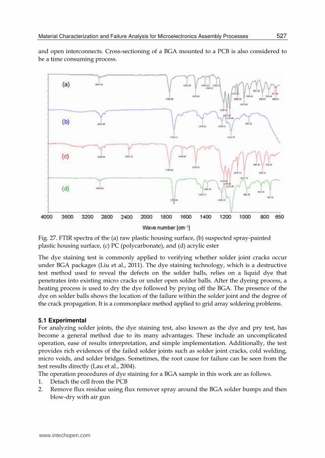
4.2.2 Case II - Plastic housing qualification Incoming quality control (IQC) and supplier quality management (SQM) found that the suspected spray-painted plastic housings had mixed in, with the raw materials, primary colors. The defect rate is about 6% for this discoloration issue after sorting. The suspected housings presented darker surfaces than the normal incoming conditions. It is difficult to recognize the difference in color between the two kinds of housings through visual inspection. Therefore, an instrumentation analysis was applied to help confirm the properties and compositions that caused the cosmetic variation. An FTIR analysis was performed to investigate the chemical structures and compositions from the housing surfaces. It is important to find out whether improper or unnecessary processes were done for the incoming materials. Clients usually attach great importance to the surface textures and dispositions of their products. The appearance of the plastic housing is shown in Fig. 26.
Fig. 26. The appearance of the plastic housing
The FTIR spectra under analysis with ATR mode from two different plastic housing surfaces are shown in Fig. 27. IR analysis was carried out at three adjacent locations for each surface to confirm the uniformity of the chemical structures. This showed very similar results from the various locations. The spectra were then compared to the FTIR built-in standard database (Fig. 27). The raw plastic housings with primary colors showed a bright surface and consistent spectrum (chemical structures) with PC (polycarbonate). The spray-painted plastic housings showed a little dark surface and consistent spectrum with acrylic ester.
5. The dye staining test
A variety of BGA packages are used in the electronic industry, for example, molded array process BGAs (MAPBGAs), plastic BGAs (PBGAs), and ceramic BGAs (CBGAs). The feature of BGA packages is such that solder balls are made to connect the packages to the printed circuit board (PCB). Once BGA packages are attached to a PCB, the inspection of the solder joints becomes necessary and is essential for failure analysis (Castello et al., 2006). Identifying a failed solder joint under the package is of some significance to the industry. However, one can only inspect the BGA outer ball row (perimeter) for failed solder joints using a microscope. X-ray inspection can provide transmission images for inner rows of balls farther under the package, but shows less information related to solder joint fractures
www.intechopen.com
Material Characterization and Failure Analysis for Microelectronics Assembly Processes
527
and open interconnects. Cross-sectioning of a BGA mounted to a PCB is also considered to be a time consuming process.
Fig. 27. FTIR spectra of the (a) raw plastic housing surface, (b) suspected spray-painted plastic housing surface, (c) PC (polycarbonate), and (d) acrylic ester
The dye staining test is commonly applied to verifying whether solder joint cracks occur under BGA packages (Liu et al., 2011). The dye staining technology, which is a destructive test method used to reveal the defects on the solder balls, relies on a liquid dye that penetrates into existing micro cracks or under open solder balls. After the dyeing process, a heating process is used to dry the dye followed by prying off the BGA. The presence of the dye on solder balls shows the location of the failure within the solder joint and the degree of the crack propagation. It is a commonplace method applied to grid array soldering problems.
5.1 Experimental For analyzing solder joints, the dye staining test, also known as the dye and pry test, has become a general method due to its many advantages. These include an uncomplicated operation, ease of results interpretation, and simple implementation. Additionally, the test provides rich evidences of the failed solder joints such as solder joint cracks, cold welding, micro voids, and solder bridges. Sometimes, the root cause for failure can be seen from the test results directly (Lau et al., 2004). The operation procedures of dye staining for a BGA sample in this work are as follows. 1. Detach the cell from the PCB 2. Remove flux residue using flux remover spray around the BGA solder bumps and then
blow-dry with air gun
www.intechopen.com

Wide Spectra of Quality Control
528
3. Clean the sample around the BGA solder bumps using isopropyl alcohol and then blow-dry with air gun
4. Repeat step 2 and 3 twice 5. Inject Dykem steel red layout fluid around the BGA component with pipe 6. Bake sample for 2 h at 125±5°C 7. Remove sample from oven and allowed to cool at room temperature 8. Bend the PCB to remove the sample mechanically Optical microscopy (Keyence VH-5500) was used to identify dyed areas from the separated package and PCB to determine the failed solder joints. For a dyed solder joint, the evidence of dye penetration shows the failure mode and the magnitude of the dye penetration.
BGA substrate
Component pad
PCB pad
PCB Laminate
Solder ball
Type 1
Type 2
Type 3
Type 4
Type 5
Type 1
Type 2
Type 3
Type 4
Type 5
BGA substrate / component pad
Within solder ball
Solder ball / PCB pad
PCB pad / PCB laminate
Component pad / solder ball
BGA substrate
Component pad
PCB pad
PCB Laminate
Solder ball
BGA substrate
Component pad
PCB pad
PCB Laminate
Solder ball
Type 1
Type 2
Type 3
Type 4
Type 5
Type 1
Type 2
Type 3
Type 4
Type 5
BGA substrate / component pad
Within solder ball
Solder ball / PCB pad
PCB pad / PCB laminate
Component pad / solder ball
Fig. 28. Failure mode classification for a solder joint
The failure mode of a solder joint can be classified into five types, as illustrated in Fig. 28. Type 1 indicates that the fracture is between the BGA substrate and the component pad. Type 2 shows that the fracture is between the component pad and the solder ball. Types 3 and 4 both show that the fracture is within the solder ball and the solder ball/PCB pad, respectively. A fracture between the PCB pad and the PCB laminate indicates Type 5. The magnitude of the dye penetration for each solder ball shows the degree of the crack propagation and can be classified into four types. Type A is such that the magnitude of dye penetration for a solder ball is below 25%. Type B falls between 26% and 50%. 51% to 75% indicates Type C. Type D has over 76% dye penetration.
5.2 Results and discussion In-circuit test (ICT) was performed on the mass-produced PCBA boards. Probes were placed back into ICT fixture locations under the CPU socket and then the press was actuated; this
www.intechopen.com

Material Characterization and Failure Analysis for Microelectronics Assembly Processes
529
(a)
(c)
(b)
(d)
(a)(a)
(c)(c)
(b)(b)
(d)(d)
Fig. 29. Optical picture of (a) PCB pad side of 1st corner (b) PCB pad side of 2nd corner (c) component BGA side of 1st corner (d) component BGA side of 2nd corner after dye staining process
Type D Type C
Type B
(a)
Type D
Type C
Type B
(b)
(c)
Type D Type C
Type B
(a)
Type D Type C
Type B
(a)
Type D
Type C
Type B
(b)
Type D
Type C
Type B
(b)
(c)(c)
Fig. 30. (a) Enlarged picture of PCB pad side of 2nd corner (b) enlarged picture of component BGA side of 2nd corner (c) the classification of magnitude regarding dye penetration for each solder balls (crack size)
www.intechopen.com

Wide Spectra of Quality Control
530
was repeated 20 times for every board. The dye staining analysis was carried out to confirm if any solder cracks occurred in CPU BGAs on the PCB. Optical microscopy was used to inspect the dyed areas and determine the failure mode classification. The test results showed that the solder balls at one outermost corner had been dyed, indicating that many solder joint cracks were found in the corner of the component. Figure 29 is an optical picture taken after the dye staining process. In order to accurately interpret the dye staining results, two photos from the PCB pad side and component BGA side are compared together to find out the right failure mode of the dyed areas. For example, Fig. 29(a) corresponds with Fig. 29(c). Dye propagation and magnitude from both sides provide the main judgment criteria regarding whether cracks occur. Following the dyeing process, the failed solder joints are identified and the failure mode classification can be defined. Figs. 30(a) and (b) are enlarged photos showing several failed solder joints. The failure mode of these solder joint cracks is between the component pad and the solder ball, which is Type 2, based on the classification of failure mode. Figure 30(c) shows the classification of the magnitude of the dye penetration. With respect to the magnitude of the dye penetration, Types B, C, and D of high percentage crack sizes can be seen in the photos indicating severe solder joint cracks occurring after a slight variation to the ICT fixture.
6. Conclusions
This study investigates PCB material performance and failure phenomenon during harsh assembly processes such as thermal shock and moisture exposure. Materials with a combination of Tg levels and Dicy / Phenolic curing agent were considered. All materials passed the assembly process verification and no PCB failure was observed. The high Tg material with a Phenolic curing agent is suggested for use in lead-free processes. Black pad is a notable failure symptom within the PCB industry and not only causes an assembly quality issue but also significantly affects product durability. For overall quality control in PCB assembly, performing reliability testing during pilot runs is essential in ensuring product quality. In this study, FTIR, SEM/EDX, and dye staining tests have been successfully used to characterize the failure samples and process materials associated with microelectronics assembly. The IR spectroscopic technique is capable of analyzing miniature samples as small as 100 μm. The characterization of process materials helps to determine the handling and/or process parameters. The sources of contaminants, such as flux, can be identified and then containment actions can be taken.
7. Acknowledgement
The authors are thankful to Jimmy Yang, Chen-Liang Ku, Hao-Chun Hsieh and all the other members of the Process Technology Team of Global Operations, Wistron Corp. for their valuable comments and involvement throughout this research. The authors are also thankful to Dr. Harvey Chang and Kenny Wang, vice-presidents of Wistron Corporation, for their great foresights to establish the analytic capabilities/expertise and financial support for the material Lab. The authors would also like to thank Dr. Kevin Chang, FT-IR specialist of PerkinElmer Taiwan Corporation, for his technical support.
www.intechopen.com

Material Characterization and Failure Analysis for Microelectronics Assembly Processes
531
8. References
Arimoto, H. (1964). α-ϒ Transition of nylon 6. Journal of Polymer Science Part A: General
Papers, Vol. 2, Iss. 5, pp. 2283-2295 Bevilacqua, M. & Ciarapica, F.E. (2004). Experiment Investigation on Electric Fans for
Domestic Appliance: Product Development and Reliability Tests. 10th ISSAT
International Reliability and Quality in Design Conference, Les Vegas, NEVADA, U.S.A., pp.45-49
Biehl, E. (2006). How to select base material for lead free applications, EIPC Winter
Conference, Budapest Bulwith, R.A., Trosky, M., Picchione L.M. & Hug, D. (2002). The black pad failure
mechanism – from beginning to end. Global SMT &packaging, pp. 9-13 Castello, T., Rooney, D., & Shangguan, D. (2006). Failure analysis techniques for lead-free
solder joints. Soldering & Surface Mount Technology, Vol. 18, No. 4, pp. 21-27 Dunaway, J.B. (1989). Residue on printed wiring assemblies: An overview and a case
history. Circuit World, Vol. 15, No. 4, pp. 28-30 Hirt, A. & Artaki, I. (1991). Non-ionic water soluble flux residue detection by XPS. Circuit
World, Vol. 17, No. 2, pp. 4-8 Huang, Y.T. & Lin, J.S. (2005). A Chi-square Test for Randomly Truncated Data. Journal of
Statistics and Computing, p67-80 Huang, C.Y., Li, M.S., Ku, C.L., Hsieh, H.C., & Li, K.C. (2009), “Chemical characterization of
failures and process materials for microelectronics assembly”, Microelectronics
International, Vol. 26 No. 3, pp. 41-48 IPC-4101B (2006). Specification for base materials for rigid and multilayer printed boards. IPC-7095A (2004). Design and Assembly Process Implementation for BGAs. pp. 32-33 IPC-A-600G (2004). Acceptability of Printed Boards IPC-TM-650 2.3.39 (1988). Surface organic contaminant identification test (infrared analytical
method). The Institute for Interconnecting and Packaging Electronic Circuits, 2215 Sanders Road, Northbrook, IL, U.S.A., pp. 60062-6135
Jayatilleka, S. & Okogbaa, G. (2003). Use of Accelerated Life Test on Transmission Belts for Prediction Product Life, Identifying Better Designs, Materials and Suppliers. Annual Reliability and Maintainability Symposium, Ottawa, Ontario, Canada, pp. 101-105
Lau, J., Shangguan, D., Castello, T., Horsley, R., Smetana, J., Hoo, N., Dauksher, W., Love, D., Menis, I., & Sullivan, B. (2004). Failure analysis of lead-free solder joints for high-density packages. Soldering & Surface Mount Technology, Vol. 16, No. 2, pp. 69-76
Lee, R.E. (1993). Scanning electron microscopy and X-ray microanalysis, PTR Prentice Hall, New Jersey
Lin, Y. & Shih, T.Y. (2007). Morphological and Microstructural Evolution of Phosphorous-Rich Layer in SnAgCu/Ni-P UBM Solder Joint. Journal of Electronic Materials, Vol. 36, No. 11, pp. 1469-1475
Liu, F., Meng, G., & Zhao, M. (2010). Experimental investigation on the failure of lead-free solder joints under drop impact. Soldering & Surface Mount Technology, Vol. 22, No. 3, pp. 36.41
Shangguan, D. & Gao, G. (1997). Lead-free and no-clean soldering for automotive electronics. Soldering & Surface Mount Technology, Vol. 9, No. 2, pp. 5-8
www.intechopen.com

Wide Spectra of Quality Control
532
Smith, C.A. (2007a). Failure analysis of electronic components and interconnection systems. Circuit World, Vol. 33, No. 1, pp. 15-21
Smith, C.A. (2007b). Chemical characterisation of materials in electronic systems using infrared spectroscopy. Circuit World, Vol. 33, No. 3, pp. 38-47
Welch, C.S. (1995). Feasibility study of OSEE inspection for flux residue on electronics assemblies. Soldering & Surface Mount Technology, Vol. 7, Iss. 1, pp. 8-11
Xu, L., Pang, J.H.L., & Che, F. (2008). Impact of Thermal Cycling on Sn-Ag-Cu Solder Joints and Board-Level Drop Reliability. Journal of Electronic Materials, Vol. 37, No. 6, pp. 880-886
Zeng, K., Stierman, R., Abbott, D., & Murtuza M. (2006). The Root Cause of Black Pad Failure of Solder Joints with Electroless Ni/Immersion Gold Plating. JOM Journal of
the Minerals, Metals and Materials Society, Volume 58, No. 6, pp. 75-79 Zhao, W., Mettas, A., Zhao, X., Vassiliou, P. & Elsayed, E.A. (2004). Generalized step stress
accelerated life model. International Conference on Business of Electronic Product
Reliability and Liability, Tucson, AZ, U.S.A., pp. 19-25
www.intechopen.com

Wide Spectra of Quality ControlEdited by Dr. Isin Akyar
ISBN 978-953-307-683-6Hard cover, 532 pagesPublisher InTechPublished online 07, July, 2011Published in print edition July, 2011
InTech EuropeUniversity Campus STeP Ri Slavka Krautzeka 83/A 51000 Rijeka, Croatia Phone: +385 (51) 770 447 Fax: +385 (51) 686 166www.intechopen.com
InTech ChinaUnit 405, Office Block, Hotel Equatorial Shanghai No.65, Yan An Road (West), Shanghai, 200040, China
Phone: +86-21-62489820 Fax: +86-21-62489821
Quality control is a standard which certainly has become a style of living. With the improvement of technologyevery day, we meet new and complicated devices and methods in different fields. Quality control explains thedirected use of testing to measure the achievement of a specific standard. It is the process, procedures andauthority used to accept or reject all components, drug product containers, closures, in-process materials,packaging material, labeling and drug products, and the authority to review production records to assure thatno errors have occurred.The quality which is supposed to be achieved is not a concept which can becontrolled by easy, numerical or other means, but it is the control over the intrinsic quality of a test facility andits studies. The aim of this book is to share useful and practical knowledge about quality control in severalfields with the people who want to improve their knowledge.
How to referenceIn order to correctly reference this scholarly work, feel free to copy and paste the following:
Chien-Yi Huang, Ming-Shu Li, Shan-Yu Huang, Cheng-I Chang and Min-Hui Huang (2011). MaterialCharacterization and Failure Analysis for Microelectronics Assembly Processes, Wide Spectra of QualityControl, Dr. Isin Akyar (Ed.), ISBN: 978-953-307-683-6, InTech, Available from:http://www.intechopen.com/books/wide-spectra-of-quality-control/material-characterization-and-failure-analysis-for-microelectronics-assembly-processes