pcb soldering inspection. structured highlight approach structured highlight method is applied to...
TRANSCRIPT

PCB Soldering Inspection
PCB Soldering Inspection
Structured Highlight approach Structured Highlight approach
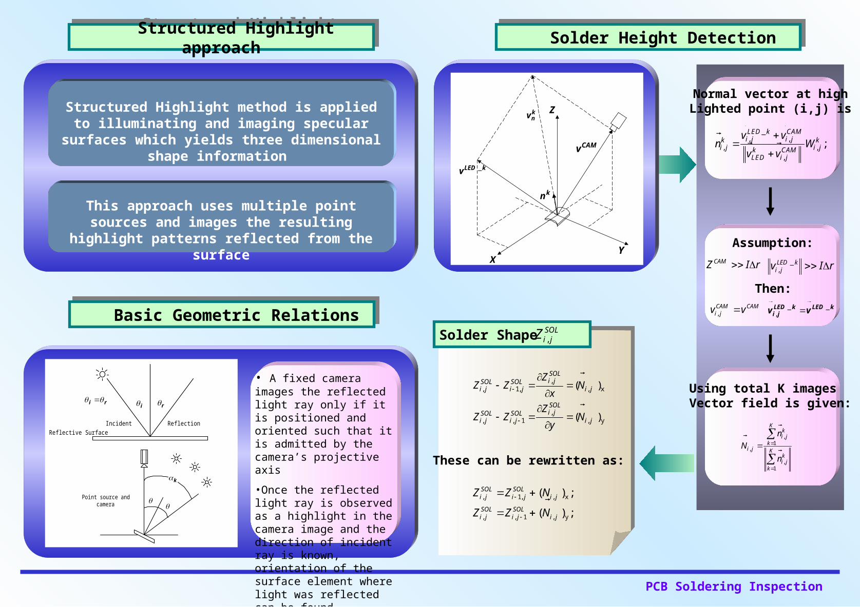
Structured Highlight method is applied to illuminating and imaging specular surfaces which
yields three dimensional shape information
This approach uses multiple point sources and images the resulting highlight patterns reflected
from the surface
Basic Geometric Relations Basic Geometric Relations
i r
Incident ReflectionReflective Surface
ri
k
Point source and
camera
• A fixed camera images the reflected light ray only if it is positioned and oriented such that it is admitted by the camera’s projective axis
•Once the reflected light ray is observed as a highlight in the camera image and the direction of incident ray is known, orientation of the surface element where light was reflected can be found
Solder Height Detection Solder Height Detection
kLEDv _
CAMv
kn
knv
X
Z
Y
Normal vector at highLighted point (i,j) is
_, ,
, ,
,
;LED k CAMi j i jk k
i j i jk CAMLED i j
v vn W
v v
rIZ CAM rIv kLEDji _
,
CAMCAMji vv
,
kLEDkLEDji vv __
,
Assumption:
Then:
Using total K imagesVector field is given:
,1
,
,1
Kki j
ki j K
ki j
k
n
N
n
Solder Shape SOLjiZ ,
,, 1, , x
,, , 1 , y
( )
( )
SOLi jSOL SOL
i j i j i j
SOLi jSOL SOL
i j i j i j
ZZ Z N
x
ZZ Z N
y
These can be rewritten as:
;) (
;) (
y,1,,
x,,1,
jiSOLji
SOLji
jiSOL
jiSOLji
NZZ
NZZ

PCB Soldering Inspection
Simulated Results Simulated Results Experimental Setup Experimental Setup
Sample PCB board images
Board Image
Processing • Find Normal vector• Vector Field• Solder Height• Depth Map
Full Depth Map
Selected Area
Reconstructed Solder Shape