240-451 vlsi, 2000 1 lecture 1 a review of microelectronics and an introduction to mos technology...
TRANSCRIPT
240-451 VLSI , 2000
1
Lecture Lecture 1 1
A review of microelectronics and an introductionto MOS technology
Department of Computer Engineering, Prince of Songkla University by Wannarat Suntiamorntut

240-451 VLSI , 2000
2
Department of Computer Engineering, Prince of Songkla University by Wannarat Suntiamorntut
Why VLSI?
Introduction to integrated circuit technology- Affected by electronics engineering technology- Characterization of electronics at present-day
integration improved the design reduces manufacturing cost

240-451 VLSI , 2000
3
Department of Computer Engineering, Prince of Songkla University by Wannarat Suntiamorntut
From design to market
Circuit Design Layout
Fabrication
Packaging Test Packaging

240-451 VLSI , 2000
4
Department of Computer Engineering, Prince of Songkla University by Wannarat Suntiamorntut
Integrated circuit (IC) era
Moore’s law : number of transistors per chip doublesevery year

240-451 VLSI , 2000
5
Department of Computer Engineering, Prince of Songkla University by Wannarat Suntiamorntut
IC technology scaling

240-451 VLSI , 2000
6
Department of Computer Engineering, Prince of Songkla University by Wannarat Suntiamorntut
Metal-oxide-semiconductor
MOS = Metal Oxide Semiconductor
In the past : Metal gate over Oxide insulationPresent-day : polycrystalline silicon that we call
“Poly”
We use metal (aluminum) for interconnection wires on the surface of the chip.

240-451 VLSI , 2000
7
Department of Computer Engineering, Prince of Songkla University by Wannarat Suntiamorntut
VLSI design process
1. Specification : Defined function, estimate cost
Adder
2. Architecture : Large block
Partition must be added in good design process if the circuit has complexity.

240-451 VLSI , 2000
8
Department of Computer Engineering, Prince of Songkla University by Wannarat Suntiamorntut
VLSI design process
3. Logic :we can divide into 3 steps - Describe the behavior of circuit (Input, Output and behavior
C = A + B- Describe the structure of circuit
R 1 R 2 R 3
Adder
A B

240-451 VLSI , 2000
9
Department of Computer Engineering, Prince of Songkla University by Wannarat Suntiamorntut
VLSI design process
- Detail design
R 1 R 2 R 3
A B

240-451 VLSI , 2000
10
Department of Computer Engineering, Prince of Songkla University by Wannarat Suntiamorntut
VLSI design process
4. Circuit Transistor : Speed, power
5. Layout :
Now we are in those 2 process (process 4 and 5 )
240-451 VLSI , 2000
11
Department of Computer Engineering, Prince of Songkla University by Wannarat Suntiamorntut
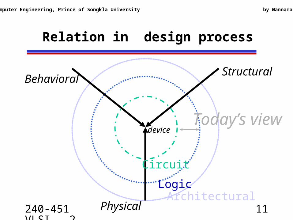
ArchitecturalLogic
Circuit
Behavioral Structural
Physical
device Today’s view
Relation in design process
240-451 VLSI , 2000
12
Department of Computer Engineering, Prince of Songkla University by Wannarat Suntiamorntut
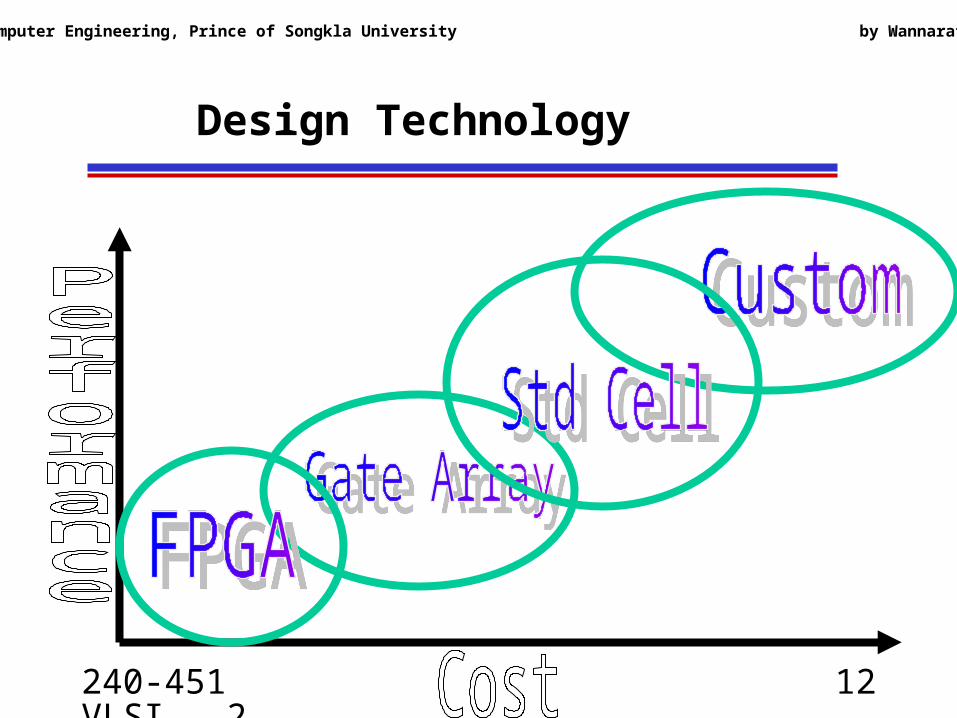
Design Technology

240-451 VLSI , 2000
13
Department of Computer Engineering, Prince of Songkla University by Wannarat Suntiamorntut
VLSI Technology
1. Schottky TTL (Transistor-transistor logic)
A
B
C= A * B
Vcc

240-451 VLSI , 2000
14
Department of Computer Engineering, Prince of Songkla University by Wannarat Suntiamorntut
VLSI Technology
2. ECL (Emitter coupled logic)
C= A + B
Vcc
C= A + B
A B
-V EE
NOR

240-451 VLSI , 2000
15
Department of Computer Engineering, Prince of Songkla University by Wannarat Suntiamorntut
3. MOS (Metal Oxide semiconductor)
VLSI Technology
VDD
C = A + BBA
NOR

240-451 VLSI , 2000
16
Department of Computer Engineering, Prince of Songkla University by Wannarat Suntiamorntut
VLSI Technology
4. CMOS (Complementary MOS)
VDD
C = A + BA
B

240-451 VLSI , 2000
17
Department of Computer Engineering, Prince of Songkla University by Wannarat Suntiamorntut
Transistor Structure

240-451 VLSI , 2000
18
Department of Computer Engineering, Prince of Songkla University by Wannarat Suntiamorntut
Manufacturing Steps
240-451 VLSI , 2000
19
Department of Computer Engineering, Prince of Songkla University by Wannarat Suntiamorntut
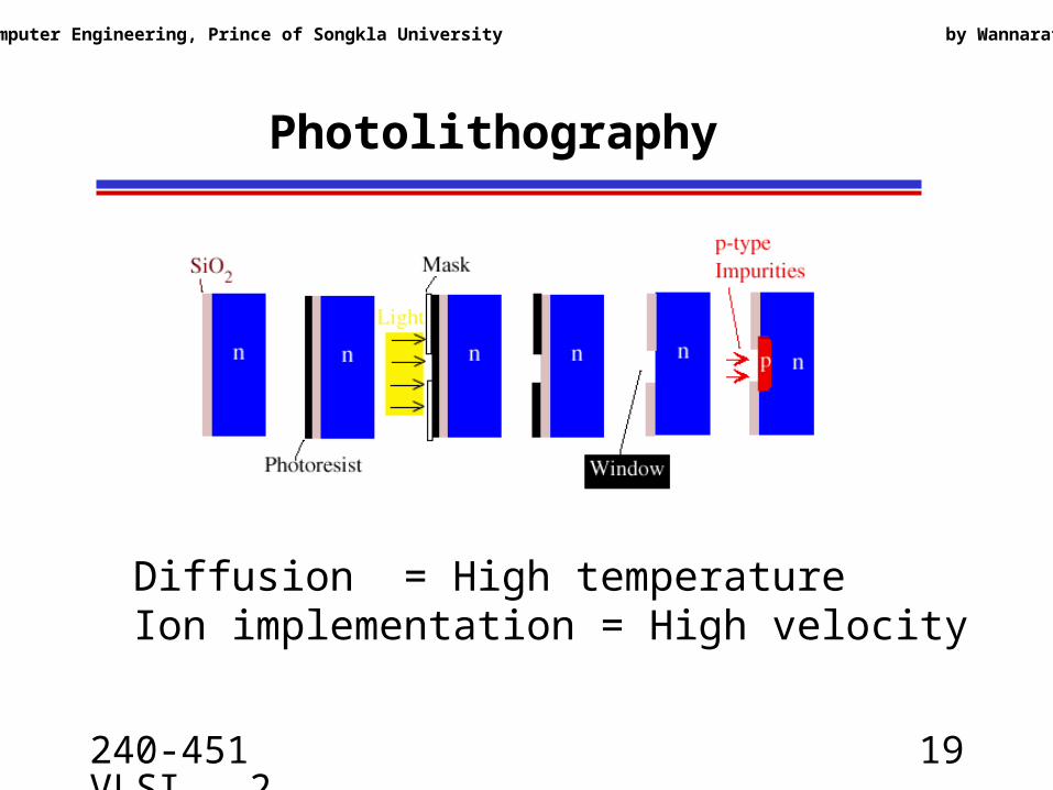
Photolithography
Diffusion = High temperatureIon implementation = High velocity

240-451 VLSI , 2000
20
Department of Computer Engineering, Prince of Songkla University by Wannarat Suntiamorntut
Process Steps
p-tub n-tub
substrate
Doped substrate for n-type, p-type transistor
240-451 VLSI , 2000
21
Department of Computer Engineering, Prince of Songkla University by Wannarat Suntiamorntut
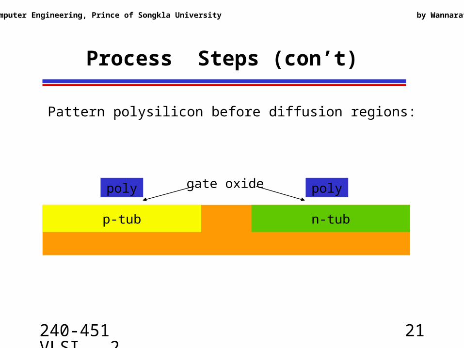
Process Steps (con’t)
Pattern polysilicon before diffusion regions:
p-tub n-tub
poly polygate oxide
240-451 VLSI , 2000
22
Department of Computer Engineering, Prince of Songkla University by Wannarat Suntiamorntut
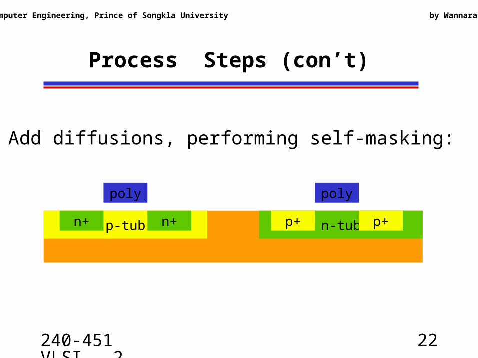
Process Steps (con’t)
p-tub n-tub
poly poly
n+n+ p+ p+
Add diffusions, performing self-masking:

240-451 VLSI , 2000
23
Department of Computer Engineering, Prince of Songkla University by Wannarat Suntiamorntut
Process Steps (con’t)
p-tub n-tub
poly poly
n+n+ p+ p+
metal 1 metal 1
vias
Start adding metal layers:

240-451 VLSI , 2000
24
Department of Computer Engineering, Prince of Songkla University by Wannarat Suntiamorntut
NMOS Process
240-451 VLSI , 2000
25
Department of Computer Engineering, Prince of Songkla University by Wannarat Suntiamorntut
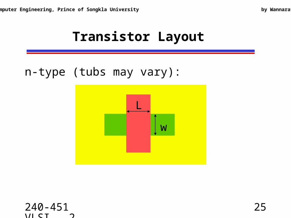
Transistor Layout
n-type (tubs may vary):
w
L

240-451 VLSI , 2000
26
Department of Computer Engineering, Prince of Songkla University by Wannarat Suntiamorntut
N-well CMOS Process
240-451 VLSI , 2000
27
Department of Computer Engineering, Prince of Songkla University by Wannarat Suntiamorntut
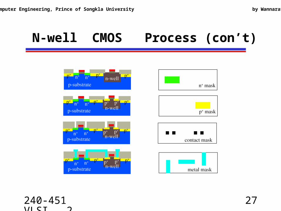
N-well CMOS Process (con’t)
240-451 VLSI , 2000
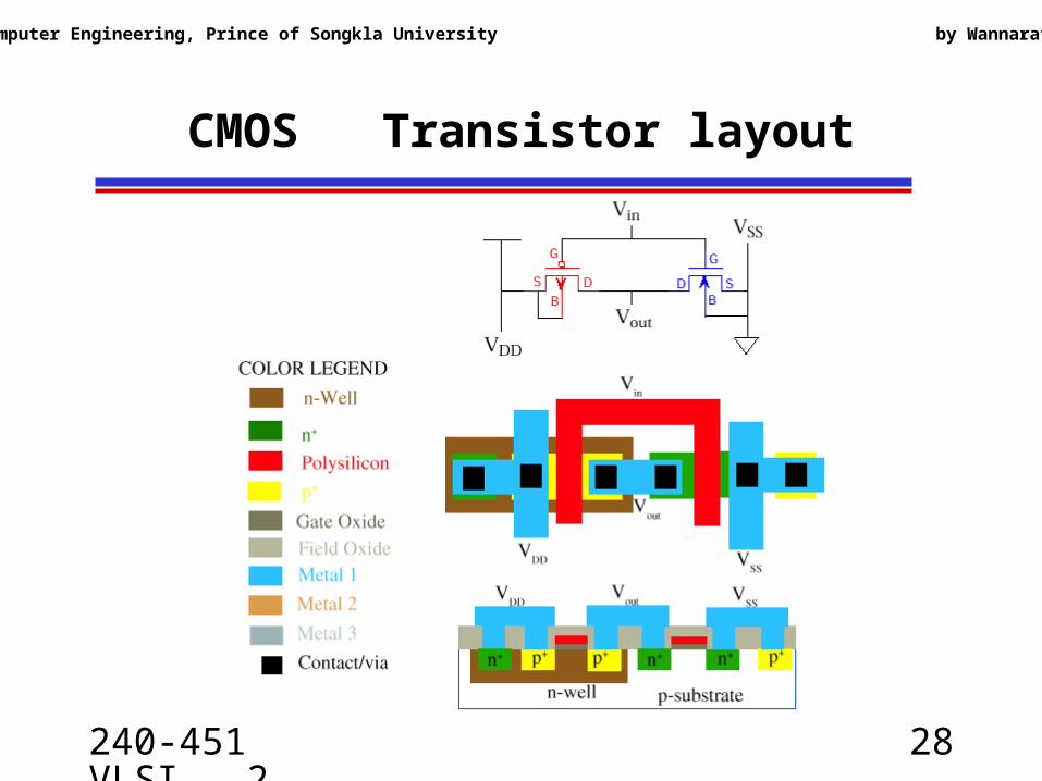
28
Department of Computer Engineering, Prince of Songkla University by Wannarat Suntiamorntut
CMOS Transistor layout

240-451 VLSI , 2000
29
Department of Computer Engineering, Prince of Songkla University by Wannarat Suntiamorntut
MOS Symbol
nMOS nMOS pMOSenhancement depletion enhancement

240-451 VLSI , 2000
30
Department of Computer Engineering, Prince of Songkla University by Wannarat Suntiamorntut
Discussion and Question