24 ghz transceiver: bgt24ltr11 - infineon technologies
TRANSCRIPT
Application Note Please read the Important Notice and Warnings at the end of this document Revision 1.4
www.infineon.com 2019-07-09
AN472
24 GHz Transceiver: BGT24LTR11
Evaluation board and system design
About this document
Scope and purpose
This application note describes the features of Infineon’s 24 GHz transceiver chipset, BGT24LTR11 MMIC and its evaluation board. It provides:
Description of all the different building blocks of the MMIC
Operation of the different blocks
Measurement data showing behaviour over temperature
VCO control using different methodologies – PTAT, PLL, and a software-based open loop
Intended audience
This document serves as a primer for users who want to get started with Infineon’s low power BGT24LTR11 MMIC for 24 GHz radar.
Related documents
Additional information can be found on www.infineon.com/24GHz
Application Note 2 Revision 1.4
2019-07-
09
24 GHz Transceiver: BGT24LTR11 Evaluation board and system design
Table of Contents
Table of Contents
About this document ....................................................................................................................... 1
Table of Contents ........................................................................................................................... 2
List of Figures ................................................................................................................................. 3
List of Tables .................................................................................................................................. 3
1 Introduction to BGT24LTR11 ........................................................................................... 4
2 Building blocks .............................................................................................................. 5
2.1 Transmitter .............................................................................................................................................. 5
2.2 Receiver ................................................................................................................................................... 6 2.3 Voltage Controlled Oscillator (VCO) ....................................................................................................... 8 2.4 Proportional to Absolute Temperature (PTAT) voltage source ............................................................. 9
2.5 Frequency divider .................................................................................................................................. 10
3 Evaluation board .......................................................................................................... 11 3.1 Schematic diagram ............................................................................................................................... 11
3.1.1 Matching structures ......................................................................................................................... 12 3.2 Layout of evaluation board ................................................................................................................... 13 3.3 Layout version improving TX to RX isolation ....................................................................................... 14
4 VCO control .................................................................................................................. 15 4.1 VCO control using PTAT ........................................................................................................................ 15 4.2 VCO control using a PLL ........................................................................................................................ 17
4.3 VCO control using a software based open-loop concept .................................................................... 18
4.3.1 Hardware setup ................................................................................................................................ 18
4.3.2 Concept ............................................................................................................................................ 19
4.3.3 Operation ......................................................................................................................................... 21
5 Authors ........................................................................................................................ 22
Revision History ............................................................................................................................ 22
Application Note 3 Revision 1.4
2019-07-
09
Introduction to BGT24LTR11
24 GHz Transceiver: BGT24LTR11 Evaluation board and system design
List of Figures
Figure 1 BGT24LTR11 Block Diagram ............................................................................................................... 4
Figure 2 TX output power vs. frequency and temperature .............................................................................. 5
Figure 3 TX output power with VTUNE connected to V_PTAT ......................................................................... 6 Figure 4 Gain vs. frequency ............................................................................................................................... 6 Figure 5 Noise figure vs. frequency ................................................................................................................... 7
Figure 6 Conversion gain vs. temperature ........................................................................................................ 7
Figure 7 Noise figure vs. temperature............................................................................................................... 8 Figure 8 VCO frequency over tuning voltage and temperature ....................................................................... 8 Figure 9 VCO frequency over temperature, VCO controlled by PTAT voltage source. Measured at random
sample. ................................................................................................................................................ 9
Figure 10 Voltage generated by PTAT voltage source vs. temperature for a random device. ......................... 9 Figure 11 Evaluation board: schematic diagram ............................................................................................. 11 Figure 12 Evaluation board: component placement ....................................................................................... 11
Figure 13 Evaluation board: matching structures on a Ro4350B substrate with a thickness of 0.254 mm ... 12
Figure 14 Evaluation board: layout with description of pin headers .............................................................. 13 Figure 15 Evaluation board: layer stack ........................................................................................................... 13 Figure 16 Evaluation board: addition of compensation structures to increase TX to RX isolation ................ 14
Figure 17 Evaluation board: compensation structures in detail. (Unit: mm) ................................................. 14 Figure 18 Block diagram: Using V_PTAT to keep BGT24LTR11 in the ISM band ............................................. 15
Figure 19 Bock diagram: VCO control using a PLL ........................................................................................... 17 Figure 20 Block diagram: VCO control using a software-based open-loop concept ...................................... 18
Figure 21 Decision function ............................................................................................................................... 20
Figure 22 Systematic timing error at the start and the end of the counting gate ........................................... 20
List of Tables
Table 1 Enabling/disabling TX output ............................................................................................................. 5 Table 2 Setting the divider ratio .................................................................................................................... 10
Table 3 Bill of materials (BOM) ...................................................................................................................... 12 Table 4 TX to RX isolation ............................................................................................................................... 14
Application Note 4 Revision 1.4
2019-07-
09
Introduction to BGT24LTR11
24 GHz Transceiver: BGT24LTR11 Evaluation board and system design
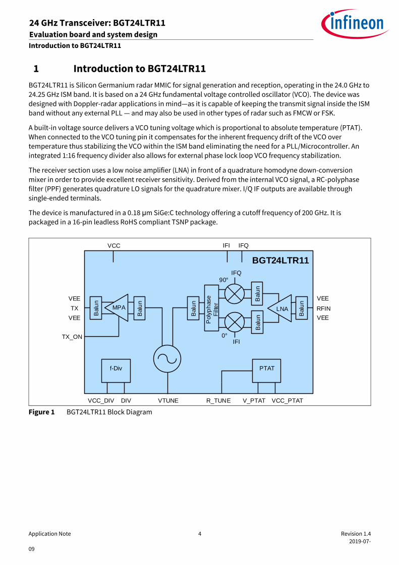
1 Introduction to BGT24LTR11
BGT24LTR11 is Silicon Germanium radar MMIC for signal generation and reception, operating in the 24.0 GHz to 24.25 GHz ISM band. It is based on a 24 GHz fundamental voltage controlled oscillator (VCO). The device was
designed with Doppler-radar applications in mind—as it is capable of keeping the transmit signal inside the ISM band without any external PLL — and may also be used in other types of radar such as FMCW or FSK.
A built-in voltage source delivers a VCO tuning voltage which is proportional to absolute temperature (PTAT). When connected to the VCO tuning pin it compensates for the inherent frequency drift of the VCO over temperature thus stabilizing the VCO within the ISM band eliminating the need for a PLL/Microcontroller. An
integrated 1:16 frequency divider also allows for external phase lock loop VCO frequency stabilization.
The receiver section uses a low noise amplifier (LNA) in front of a quadrature homodyne down-conversion
mixer in order to provide excellent receiver sensitivity. Derived from the internal VCO signal, a RC-polyphase filter (PPF) generates quadrature LO signals for the quadrature mixer. I/Q IF outputs are available through single-ended terminals.
The device is manufactured in a 0.18 μm SiGe:C technology offering a cutoff frequency of 200 GHz. It is packaged in a 16-pin leadless RoHS compliant TSNP package.
VCC
VEE
PTAT
IFI IFQ
RFINTX
f-Div
90°
0°
Poly
ph
ase
Filte
r
Balu
n
Balu
n
MPAB
alu
nBalu
nB
alu
n
LNA
Balu
n
VEE
VEE
VEE
VTUNE V_PTATDIV VCC_PTATVCC_DIV R_TUNE
TX_ON
IFQ
IFI
BGT24LTR11
Figure 1 BGT24LTR11 Block Diagram
Application Note 5 Revision 1.4
2019-07-
09
Building blocks
24 GHz Transceiver: BGT24LTR11 Evaluation board and system design
2 Building blocks
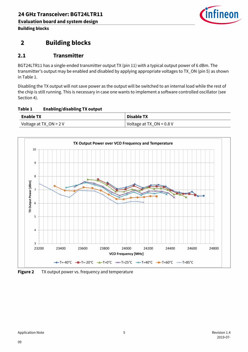
2.1 Transmitter
BGT24LTR11 has a single-ended transmitter output TX (pin 11) with a typical output power of 6 dBm. The
transmitter’s output may be enabled and disabled by applying appropriate voltages to TX_ON (pin 5) as shown in Table 1.
Disabling the TX output will not save power as the output will be switched to an internal load while the rest of
the chip is still running. This is necessary in case one wants to implement a software controlled oscillator (see
Section 4).
Table 1 Enabling/disabling TX output
Enable TX Disable TX
Voltage at TX_ON > 2 V Voltage at TX_ON < 0.8 V
Figure 2 TX output power vs. frequency and temperature
3
4
5
6
7
8
9
10
23200 23400 23600 23800 24000 24200 24400 24600 24800
TX O
utp
ut
Po
wer
[d
Bm
]
VCO Frequency [MHz]
TX Output Power over VCO Frequency and Temperature
T=-40°C T=-20°C T=0°C T=25°C T=40°C T=60°C T=85°C
Application Note 6 Revision 1.4
2019-07-
09
Building blocks
24 GHz Transceiver: BGT24LTR11 Evaluation board and system design
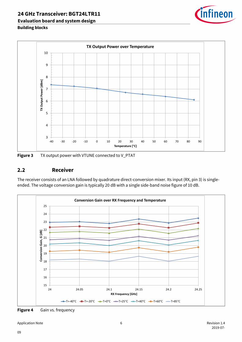
Figure 3 TX output power with VTUNE connected to V_PTAT
2.2 Receiver
The receiver consists of an LNA followed by quadrature direct-conversion mixer. Its input (RX, pin 3) is single-ended. The voltage conversion gain is typically 20 dB with a single side-band noise figure of 10 dB.
Figure 4 Gain vs. frequency
3
4
5
6
7
8
9
10
-40 -30 -20 -10 0 10 20 30 40 50 60 70 80 90
TX O
utp
ut
Po
we
r [d
Bm
]
Temperature [°C]
TX Output Power over Temperature
15
16
17
18
19
20
21
22
23
24
25
24 24.05 24.1 24.15 24.2 24.25
Co
nve
rsio
n G
ain
, G [
dB
]
RX Frequency [GHz]
Conversion Gain over RX Frequency and Temperature
T=-40°C T=-20°C T=0°C T=25°C T=40°C T=60°C T=85°C

Application Note 7 Revision 1.4
2019-07-
09
Building blocks
24 GHz Transceiver: BGT24LTR11 Evaluation board and system design
Figure 5 Noise figure vs. frequency
Figure 6 Conversion gain vs. temperature
5
6
7
8
9
10
11
12
13
14
15
24 24.05 24.1 24.15 24.2 24.25
No
ise
Fig
ure
, NF
[dB
]
RX Frequency [GHz]
Noise Figure over RX Frequency and Temperature
T=-40°C T=-20°C T=0°C T=25°C T=40°C T=60°C T=85°C
16
17
18
19
20
21
22
23
24
-40 -20 0 20 40 60 80 100
Co
nve
rsio
n G
ain
, G [
dB
]
Temperature [°C]
Conversion Gain over Rx Frequency and Temperature
Rx=24GHz Rx=24.05GHz Rx=24.1GHz Rx=24.15GHz Rx=24.2GHz Rx=24.25GHz
Application Note 8 Revision 1.4
2019-07-
09
Building blocks
24 GHz Transceiver: BGT24LTR11 Evaluation board and system design
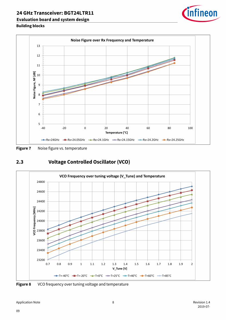
Figure 7 Noise figure vs. temperature
2.3 Voltage Controlled Oscillator (VCO)
Figure 8 VCO frequency over tuning voltage and temperature
5
6
7
8
9
10
11
12
13
-40 -20 0 20 40 60 80 100
No
ise
Fig
ure
, NF
[dB
]
Temperature [°C]
Noise Figure over Rx Frequency and Temperature
Rx=24GHz Rx=24.05GHz Rx=24.1GHz Rx=24.15GHz Rx=24.2GHz Rx=24.25GHz
23200
23400
23600
23800
24000
24200
24400
24600
24800
0.7 0.8 0.9 1 1.1 1.2 1.3 1.4 1.5 1.6 1.7 1.8 1.9 2
VC
O F
req
ue
ncy
[M
Hz]
V_Tune [V]
VCO Frequency over tuning voltage (V_Tune) and Temperature
T=-40°C T=-20°C T=0°C T=25°C T=40°C T=60°C T=85°C
Application Note 9 Revision 1.4
2019-07-
09
Building blocks
24 GHz Transceiver: BGT24LTR11 Evaluation board and system design
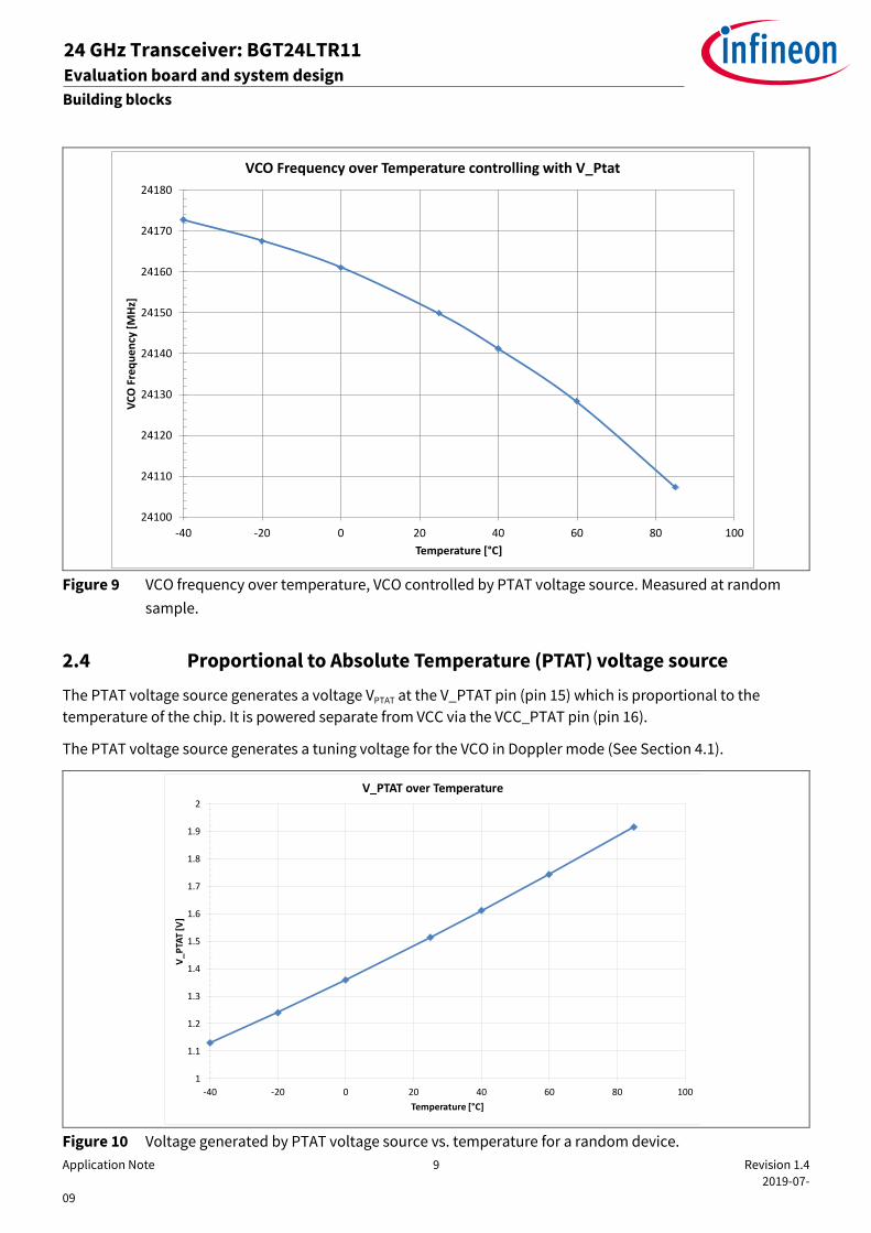
Figure 9 VCO frequency over temperature, VCO controlled by PTAT voltage source. Measured at random
sample.
2.4 Proportional to Absolute Temperature (PTAT) voltage source
The PTAT voltage source generates a voltage VPTAT at the V_PTAT pin (pin 15) which is proportional to the
temperature of the chip. It is powered separate from VCC via the VCC_PTAT pin (pin 16).
The PTAT voltage source generates a tuning voltage for the VCO in Doppler mode (See Section 4.1).
Figure 10 Voltage generated by PTAT voltage source vs. temperature for a random device.
24100
24110
24120
24130
24140
24150
24160
24170
24180
-40 -20 0 20 40 60 80 100
VC
O F
req
ue
ncy
[M
Hz]
Temperature [°C]
VCO Frequency over Temperature controlling with V_Ptat
1
1.1
1.2
1.3
1.4
1.5
1.6
1.7
1.8
1.9
2
-40 -20 0 20 40 60 80 100
V_P
TAT
[V]
Temperature [°C]
V_PTAT over Temperature
Application Note 10 Revision 1.4
2019-07-
09
Building blocks
24 GHz Transceiver: BGT24LTR11 Evaluation board and system design
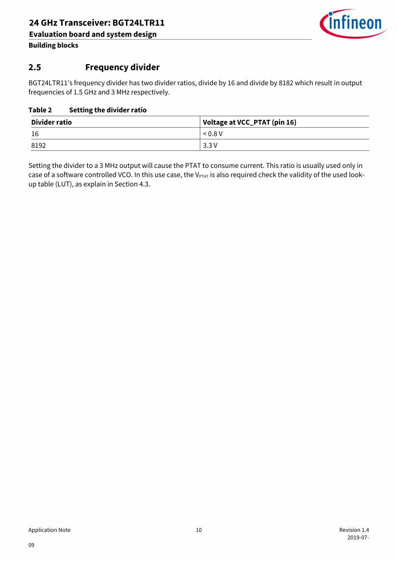
2.5 Frequency divider
BGT24LTR11’s frequency divider has two divider ratios, divide by 16 and divide by 8182 which result in output frequencies of 1.5 GHz and 3 MHz respectively.
Table 2 Setting the divider ratio
Divider ratio Voltage at VCC_PTAT (pin 16)
16 < 0.8 V
8192 3.3 V
Setting the divider to a 3 MHz output will cause the PTAT to consume current. This ratio is usually used only in
case of a software controlled VCO. In this use case, the VPTAT is also required check the validity of the used look-
up table (LUT), as explain in Section 4.3.
Application Note 11 Revision 1.4
2019-07-
09
Evaluation board
24 GHz Transceiver: BGT24LTR11 Evaluation board and system design
3 Evaluation board
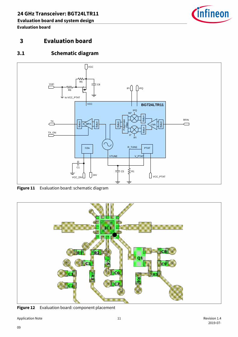
3.1 Schematic diagram
VCC
PTAT
IFI IFQ
RFINTX
f-Div
90°
0°
Poly
ph
ase
Filte
r
Balu
n
Balu
n
MPA
Balu
nBalu
nB
alu
n
LNA
Balu
n
VTUNE V_PTAT
DIVVCC_PTATVCC_DIV
R_TUNE
TX_ON
C8R5
R6
Vctrl
VCC
to VCC_PTAT
C5
C1
R1
IFQ
IFI
BGT24LTR11
Figure 11 Evaluation board: schematic diagram
Figure 12 Evaluation board: component placement
Application Note 12 Revision 1.4
2019-07-
09
Evaluation board
24 GHz Transceiver: BGT24LTR11 Evaluation board and system design
Table 3 Bill of materials (BOM)
Designation Part type Value Package Manufacturer
C1, C5, C8 Chip capacitor 1 µF 0402 Various
C2, C3, C6, C7, C9 DNP 0402
R1 Chip resistor 16 kΩ 0402 Various
R2,R3 Chip resistor 0 Ω 0402 Various
R5 Chip resistor 100 kΩ 0402 Various
R6 Chip resistor 1 kΩ 0402 Various
Q1 p-MOSFET BSS209PW SOT-323 Infineon
IC1 Radar MMIC BGT24LTR11N16 TSNP-16-9 Infineon
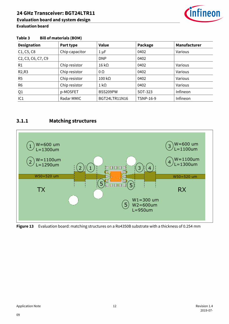
3.1.1 Matching structures
Figure 13 Evaluation board: matching structures on a Ro4350B substrate with a thickness of 0.254 mm
W50=520 um
TX RX
W50=520 um
12 43
W=600 umL=1300um
W=1100umL=1290um
1
2
W=600 umL=1100um
W=1100umL=1300um
3
4
5 5
5W1=300 umW2=600umL=950um
Application Note 13 Revision 1.4
2019-07-
09
Evaluation board
24 GHz Transceiver: BGT24LTR11 Evaluation board and system design
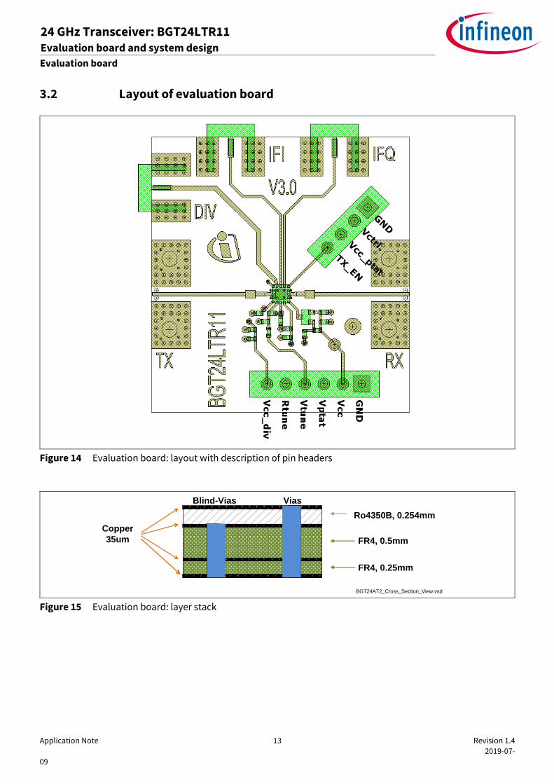
3.2 Layout of evaluation board
Figure 14 Evaluation board: layout with description of pin headers
Figure 15 Evaluation board: layer stack
Copper
35um
Blind-Vias Vias
Ro4350B, 0.254mm
FR4, 0.5mm
BGT24AT2_Cross_Section_View.vsd
FR4, 0.25mm
Application Note 14 Revision 1.4
2019-07-
09
Evaluation board
24 GHz Transceiver: BGT24LTR11 Evaluation board and system design
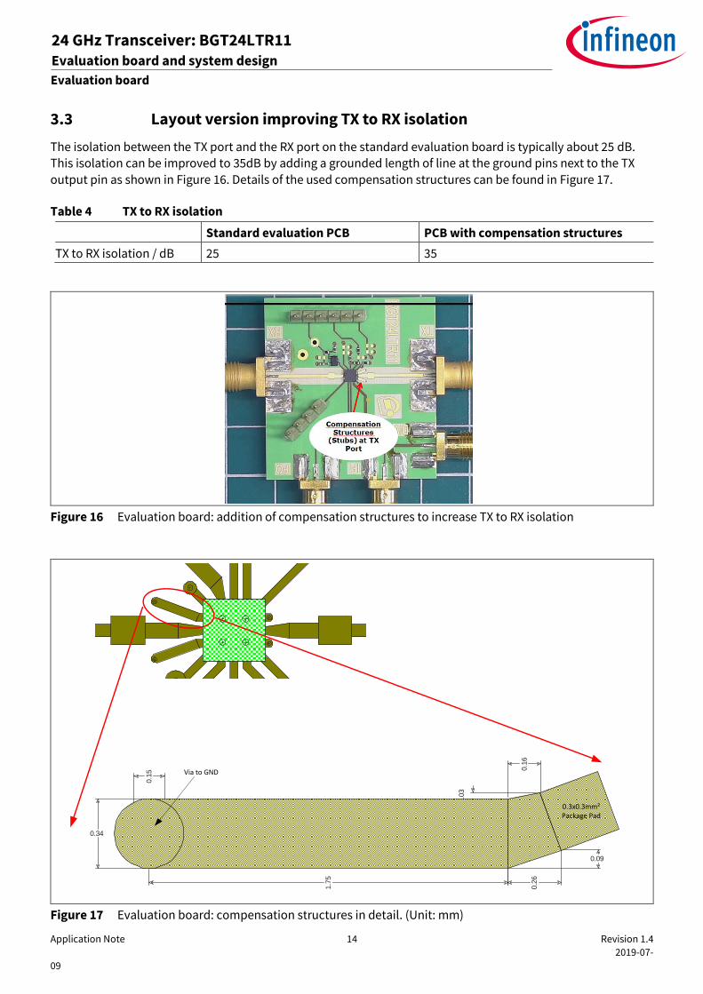
3.3 Layout version improving TX to RX isolation
The isolation between the TX port and the RX port on the standard evaluation board is typically about 25 dB. This isolation can be improved to 35dB by adding a grounded length of line at the ground pins next to the TX
output pin as shown in Figure 16. Details of the used compensation structures can be found in Figure 17.
Table 4 TX to RX isolation
Standard evaluation PCB PCB with compensation structures
TX to RX isolation / dB 25 35
Figure 16 Evaluation board: addition of compensation structures to increase TX to RX isolation
Figure 17 Evaluation board: compensation structures in detail. (Unit: mm)
0.0
3
0.1
6
0.09
0.2
6
0.1
5
1.7
5
0.34
0.3x0.3mm²Package Pad
Via to GND
Application Note 15 Revision 1.4
2019-07-
09
VCO control
24 GHz Transceiver: BGT24LTR11 Evaluation board and system design
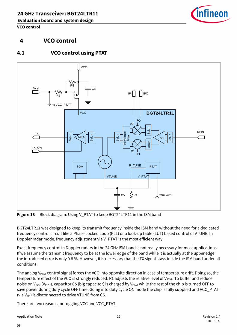
4 VCO control
4.1 VCO control using PTAT
VCC
PTAT
IFI IFQ
RFINTX
f-Div
90°
0°
Poly
ph
ase
Filte
r
Balu
n
Balu
n
MPA
Balu
nBalu
nB
alu
n
LNA
Balu
n
VTUNE V_PTAT
from Vctrl
R_TUNE
TX_ON
C8R5
R6
Vctrl
VCC
to VCC_PTAT
C5 R1
IFQ
IFI
BGT24LTR11
Figure 18 Block diagram: Using V_PTAT to keep BGT24LTR11 in the ISM band
BGT24LTR11 was designed to keep its transmit frequency inside the ISM band without the need for a dedicated frequency control circuit like a Phase Locked Loop (PLL) or a look-up table (LUT) based control of VTUNE. In
Doppler radar mode, frequency adjustment via V_PTAT is the most efficient way.
Exact frequency control in Doppler radars in the 24 GHz ISM band is not really necessary for most applications. If we assume the transmit frequency to be at the lower edge of the band while it is actually at the upper edge the introduced error is only 0.8 %. However, it is necessary that the TX signal stays inside the ISM band under all conditions.
The analog VPTAT control signal forces the VCO into opposite direction in case of temperature drift. Doing so, the temperature effect of the VCO is strongly reduced. R1 adjusts the relative level of VPTAT. To buffer and reduce
noise on Vtune (VPTAT), capacitor C5 (big capacitor) is charged by VPTAT while the rest of the chip is turned OFF to save power during duty cycle OFF time. Going into duty cycle ON mode the chip is fully supplied and VCC_PTAT (via Vctrl) is disconnected to drive VTUNE from C5.
There are two reasons for toggling VCC and VCC_PTAT:
Application Note 16 Revision 1.4
2019-07-
09
VCO control
24 GHz Transceiver: BGT24LTR11 Evaluation board and system design
Turning off VCC and VCC_PTAT reduces current consumption (45 mA and 1.5mA, respectively)
The PTAT source generates noise at its output when running and this noise on the tuning voltage will degrade the signal to noise ratio (SNR) of the system. However, for some short range this SNR might still be acceptable.
Operation:
1. TX_ON = 0 V. Disables TX output to prevent out of band emissions.
2. Vctrl = 3.3 V. This turns on the PTAT source (VCC_PTAT = 3.3 V) while VCC line for the entire RF stage including the VCO is disconnected from the power supply.
3. Wait for C5 to be charged. At the start-up of the system when the capacitor is fully discharged this will require a longer time. During normal operation the capacitor is only slightly discharged and will be very
quickly recharged.
4. Vctrl = 0 V. Turn off PTAT and turn on the rest of the chip (RF with VCO).
5. Wait for VCO to settle its frequency. Settling time of the VCO is maximum 100 ns.
6. TX_ON = 3.3 V. Enables TX output. TX_ON should be delayed by about 200ns vs. RF section ON (Vctrl = 0 V) to keep TX signal clean.
7. Sample IF frequency.
8. Go to 1.
Further reduction of the power consumption is possible by introducing a time frame when both VCC and
VCC_PTAT are disconnected. This would mean that VCC_PTAT needs to be disconnected from Vctrl and one more independent GPIO pin needs to be available at the microcontroller (MCU) in the system.
Application Note 17 Revision 1.4
2019-07-
09
VCO control
24 GHz Transceiver: BGT24LTR11 Evaluation board and system design
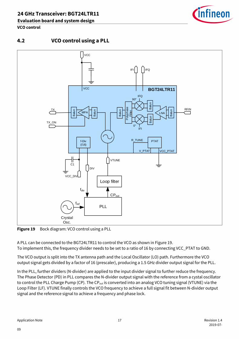
4.2 VCO control using a PLL
VCC
PTAT
IFI IFQ
RFINTX
f-Div
(/16)
90°
0°P
oly
ph
ase
Filte
r
Balu
n
Balu
n
MPA
Balu
nBalu
nB
alu
n
LNA
Balu
n
V_PTAT
R_TUNE
TX_ON
VCC
VCC_DIV
DIV
C1
VTUNE
PLL
VCC_PTAT
Loop filter
fref
fdiv
CPout
Crystal
Osc.
IFQ
IFI
BGT24LTR11
Figure 19 Bock diagram: VCO control using a PLL
A PLL can be connected to the BGT24LTR11 to control the VCO as shown in Figure 19.
To implement this, the frequency divider needs to be set to a ratio of 16 by connecting VCC_PTAT to GND.
The VCO output is split into the TX antenna path and the Local Oscillator (LO) path. Furthermore the VCO
output signal gets divided by a factor of 16 (prescaler), producing a 1.5 GHz divider output signal for the PLL.
In the PLL, further dividers (N-divider) are applied to the input divider signal to further reduce the frequency. The Phase Detector (PD) in PLL compares the N-divider output signal with the reference from a cystal oscillator to control the PLL Charge Pump (CP). The CPout is converted into an analog VCO tuning signal (VTUNE) via the Loop Filter (LF). VTUNE finally controls the VCO frequency to achieve a full signal fit between N-divider output
signal and the reference signal to achieve a frequency and phase lock.
Application Note 18 Revision 1.4
2019-07-
09
VCO control
24 GHz Transceiver: BGT24LTR11 Evaluation board and system design
4.3 VCO control using a software based open-loop concept
It is possible to control BGT24LTR11 using a software-based open loop concept. In this approach, a loop is needed with a voltage source and a feedback which is used to adapt the needed frequency changes. This
implementation has the advantage of reducing the PCB space, BOM cost and power consumption by
eliminating the HW PLL. In this software based open-loop concept – often called as ‘Software PLL’ – there is no VCO phase and frequency locking to a reference signal. Frequency is measured periodically and VCO is tuned accordingly. VCO
Phase Noise (PN) is comparable to the free-wheeling VCO (best case) and not improved like the HW PLL can do.
However, VCO PN is less critical in Short Range Radar applications, because PN in the TX, RX and LO path stays mainly correlated for short target distances, resulting is a strong reduction of residual PN in the downmixed IF. (referring to: Range Correlation Effect).
Both Doppler radar and stepped-FMCW radar can be realized with this software based open-loop VCO
adjustment/sweeping concept. System-performance might be lower than a HW PLL, but is often sufficient for a lot of applications like smart lighting or proximity detection etc.
4.3.1 Hardware setup
VCC
PTAT
IFI IFQ
RFINTX
f-Div
(/8192)
90°
0°
Poly
ph
ase
Filte
r
Balu
n
Balu
n
MPA
Balu
nBalu
nB
alu
n
LNA
Balu
n
V_PTAT
R_TUNE
VCC
TX_ON
VCC_DIVDIV
VTUNE
CCU
VCC
LUT ADC
MCU
Temperature
DAC
RC filter
DECISION
FUNCTION
BGT24LTR11
GPIO
IFQ
IFI
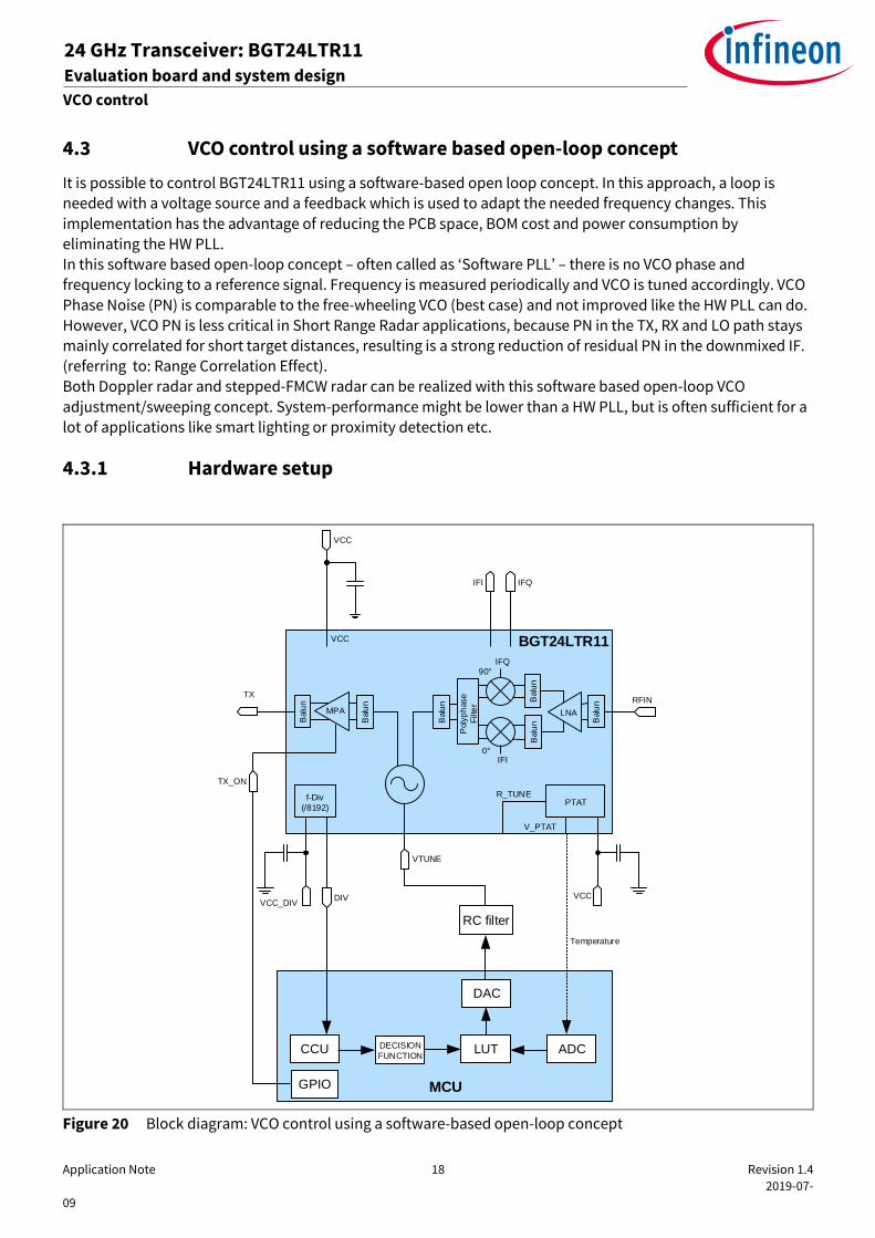
Figure 20 Block diagram: VCO control using a software-based open-loop concept
Application Note 19 Revision 1.4
2019-07-
09
VCO control
24 GHz Transceiver: BGT24LTR11 Evaluation board and system design
Figure 20 shows a block diagram on how to set-up the system.
Connect VCC_DIV and VCC_PTAT to VCC to set the divider ratio to 8192.
Connect divider output to a Capture & Compare Unit (CCU) of the MCU to determine the frequency of the oscillator.
Connect MCU’s DAC output to the V_TUNE of BGT24LTR11 through a 2-stage RC filter to provide a tuning voltage to the VCO.
The 2-stage RC DAC filter is required to filter the noise and reject the higher unwanted frequencies. It should be placed as close to the VCO V_TUNE input as possible.
The design of this RC DAC filter is critical to avoid VCO modulation with noise and spurs. For a stepped-
FMCW approach, the DAC filter needs to be optimized for the update rate based on the chirp time (Tc) and number of samples per chirp (Nsamples). For example, for a Tc = 1500 ms and Nsamples = 256, the update
rate is 1500ms/256 = 6 µs (step-time). Therefore, the RC time constant for the DAC filter should be designed to settle at 5 µs (90…95% of desired voltage step). This lets the DAC’s output voltage and consequently the VCO frequency to be in a steady state at the end of step-time when the baseband ADC is trigged for measurement.
As an option, connect the V_PTAT output from BGT24LTR11 to an ADC channel of the MCU to determine the
temperature of the chip. This would allow to compensate the frequency shift due to temperature changes and would reduce the need to re-calibrate the SW-PLL very frequently.
4.3.2 Concept
As shown in Figure 20, the DAC of the MCU is used to generate a tuning voltage for the VCO input. Vtune is generated by the DAC for the start frequency and then filtered in the RC-filter (2 stages). According to the Vtune
input, the VCO produces the TX/LO signal. The VCO signal is also fed into a frequency divider and gets divided
by a factor of 8192. This divided signal is captured by the CCU in the MCU. The divider output signal is measured by counting the number of rising/falling (or both) edges of the MCU’s master clock inside a certain number of divider output signal periods (counting gate). The measured frequency is then compared with the required
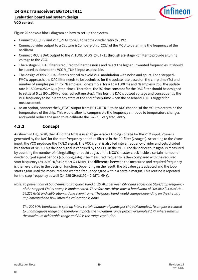
start frequency (24.025GHz/8192 = 2.9327 MHz). The difference between the measured and required frequency is then evaluated in the decision function. Depending on the result, the bit value gets adapted and the loop
starts again until the measured and wanted frequency agree within a certain margin. This routine is repeated for the stop frequency as well (24.225 GHz/8192 = 2.9571 MHz).
Note: To prevent out of band emissions a guard band of 25 MHz between ISM band edges and Start/Stop frequency of the stepped-FMCW sweep is implemented. Therefore the chirps have a bandwidth of 200 MHz (24.025GHz -
24.225 GHz) and calibration is done every frame. The guard band would change depending on the circuitry implemented and how often the calibration is done.
The 200 MHz bandwidth is split up into a certain number of points per chirp (Nsamples). Nsamples is related
to unambiguous range and therefore impacts the maximum range (Rmax =Nsamples*∆R), where Rmax is the maximum achievable range and ∆R is the range resolution.
Application Note 20 Revision 1.4
2019-07-
09
VCO control
24 GHz Transceiver: BGT24LTR11 Evaluation board and system design
CCUDivided Signal</> wanted frequency
increase bitssmaller
lower bitshigher
new bit value
Figure 21 Decision function
The length of the counting gate has a strong impact on the accuracy of the VCO frequency measurement. At the start and at the end of the counting gate (N times the period of the divider output signal), there is a systematic error caused by the period of the MCU master clock. Longer counting gate time (i.e., more number of periods of the MCU master clock – e.g. 80MHz – are counted) results in a lower impact of this systematic error
on VCO frequency measurement accuracy. However, longer counting gate time results in a longer ON time for the BGT24LTR11 and impacts the overall power consumption.
T_gate = t_q1 = counting gate time
T_masterclk
1st rising
edge (01)
Last rising=8
Counter = 8
01 02 03 04 05 06 0807
01 03020201 03 04 0606050504 07 07Master clock
(f_masterclk)
Divider output
(f_q1)
N_ticks
t_q1
1st rising
edge (01)
05 06 0807
t_q1
Last rising=15
Counter = 15
09 10 11 12 151413
0606050504 07 07 08 10090908 10 11 1313121211 14 14 15
01 02 03 04
01 03020201 03 04
T_gate =N*t_q1= counting gate time
T_masterclk
Master clock
(f_masterclk)
Divider output
(f_q1)
N_ticks
Counting error
VCO freq is lower
Counting error
VCO freq is higher
Desired VCO freq (f_desired): 24.025 GHz
Divider output frequency (f_q1): 24.025 GHz/8192: 2.9327 MHz
Master clock frequency (f_masterclk): 80 MHz
Divider output period (t_q1)= 1/2.9327 MHz = 340.98 ns
Master clock period (t_masterclk): 1/80 MHz: 12.5 ns
Number of divider output periods (N) = 100
Counting gate time (T_gate) = N*t_q1 = 100*340.98 ns = 34098 ns
No. of ticks (N_ticks) = T_gate/t_masterclk = 34098ns/12.5 ns = 2728
Obtained VCO freq (f_measured): (8192*N/N_ticks*t_masterclk) = 8192*100/2728*12.5ns = 24.023 GHz
Error = f_desired – f_measured = 24.025 – 24.023 GHz = 2 MHz
Figure 22 Systematic timing error at the start and the end of the counting gate

Application Note 21 Revision 1.4
2019-07-
09
VCO control
24 GHz Transceiver: BGT24LTR11 Evaluation board and system design
For a divider output frequency of ~3MHz and a MCU master clock of 80 MHz, we recommend to count over 100 periods (N=100) of the divider output signal, to get a maximal frequency measurement error < 10 MHz.
Another way to reduce this systematic timing error would be to increase the master clock frequency (for example, a master clock of 120 MHz instead of 80 MHz will reduce the error as the T_clock time will be reduced from 12.5 ns to 8.3 ns, and the maximal frequency measurement error is < 6 MHz). However, higher master clock
frequency leads to higher power consumption by the microcontroller.
Note: To stay inside the ISM band during the frequency search process, the smart search for the start frequency begins always with a DAC value generating a VCO frequency above the desired start frequency. Similarly, stop frequency search should begin below the desired stop frequency.
With the achieved start- and stop frequency DAC values (and Vtune values) a linear interpolation can be done
and a look-up-table (LUT) “DAC value vs. VCO Frequency” is generated. The contents of the LUT are clocked (e.g. via DMA) to the DAC and hence provide the modulation of the VCO.
To further improve the linearity of the chirps, it is possible to do a search for three or more frequency points and perform a polynomial approximation between these points to fit the Vtune vs. VCO Frequency in a more precise non-linear LUT. Also, by utilizing chip’s temperature information (e.g. via PTAT), the LUT can be re-
calibrated only when there is a change in chip’s temperature. This would reduce the need to calibrate the LUT very frequently.
4.3.3 Operation
1. To get best frequency measurement accuracy (NO VCO pulling effect), TX should remain ON during the
frequency search process. VTUNE must keep the VCO in the ISM band all the time by following the ‘smart
search’ methodology from Section 4.3.2.
2. Check the temperature of the chip using the VPTAT. (if implemented)
3. Set the DAC to a fixed starting value for start frequency search to generate a VTUNE voltage for the VCO.
4. CCU measures the frequency of the divider output signal. The desired start frequency is already known and compared with the measured frequency. The DAC value is then adjusted using a decision function to
achieve the best possible match for the desired frequency. (iterative frequency search process)
5. Once the DAC value for the start frequency is found, repeat the steps 3&4 to search the appropriate DAC
value for the stop frequency.
6. Using these start and stop DAC values, generate a Look-Up Table (LUT) that gives the DAC values
corresponding to different VCO frequencies.
7. Use the generated LUT for the modulation of the VCO by clocking the LUT values (e.g. via DMA) to the
DAC. Feed the DAC output to the DAC filter. After the DAC filter output has settled on the step, take the
ADC measurement and then move the DAC to the next LUT step, creating a stepped-FMCW chirp.
8. Check the temperature of the chip. If the temperature changed, or it is the beginning of a new frame go
to 1 else go to 7 to generate the next chirp.
Application Note 22 Revision 1.4
2019-07-
09
Authors
24 GHz Transceiver: BGT24LTR11 Evaluation board and system design
5 Authors
Radar Application Engineering Team, Business Line “Radio Frequency and Sensors”
Revision History
Major changes since the last revision
Page or Reference Description of change
8 f Corrections to PTAT source
Section 4 More detailed description of the VCO control through PTAT, PLL and Software-
controlled loop
Trademarks of Infineon Technologies AG µHVIC™, µIPM™, µPFC™, AU-ConvertIR™, AURIX™, C166™, CanPAK™, CIPOS™, CIPURSE™, CoolDP™, CoolGaN™, COOLiR™, CoolMOS™, CoolSET™, CoolSiC™, DAVE™, DI-POL™, DirectFET™, DrBlade™, EasyPIM™, EconoBRIDGE™, EconoDUAL™, EconoPACK™, EconoPIM™, EiceDRIVER™, eupec™, FCOS™, GaNpowIR™, HEXFET™, HITFET™, HybridPACK™, iMOTION™, IRAM™, ISOFACE™, IsoPACK™, LEDrivIR™, LITIX™, MIPAQ™, ModSTACK™, my-d™, NovalithIC™, OPTIGA™, OptiMOS™, ORIGA™, PowIRaudio™, PowIRStage™, PrimePACK™, PrimeSTACK™, PROFET™, PRO-SIL™, RASIC™, REAL3™, SmartLEWIS™, SOLID FLASH™, SPOC™, StrongIRFET™, SupIRBuck™, TEMPFET™, TRENCHSTOP™, TriCore™, UHVIC™, XHP™, XMC™ Trademarks updated November 2015
Other Trademarks All referenced product or service names and trademarks are the property of their respective owners. ifx1owners.
Edition 2019-07-09
AN_472_2016_03_PL32_001
Published by
Infineon Technologies AG
81726 Munich, Germany
© 2019 Infineon Technologies AG.
All Rights Reserved.
Do you have a question about this
document?
Email: [email protected]
Document reference
IMPORTANT NOTICE The information contained in this application note is given as a hint for the implementation of the product only and shall in no event be regarded as a description or warranty of a certain functionality, condition or quality of the product. Before implementation of the product, the recipient of this application note must verify any function and other technical information given herein in the real application. Infineon Technologies hereby disclaims any and all warranties and liabilities of any kind (including without limitation warranties of non-infringement of intellectual property rights of any third party) with respect to any and all information given in this application note. The data contained in this document is exclusively intended for technically trained staff. It is the responsibility of customer’s technical departments to evaluate the suitability of the product for the intended application and the completeness of the product information given in this document with respect to such application.
For further information on the product, technology, delivery terms and conditions and prices please contact your nearest Infineon Technologies office (www.infineon.com).
WARNINGS Due to technical requirements products may contain dangerous substances. For information on the types in question please contact your nearest Infineon Technologies office. Except as otherwise explicitly approved by Infineon Technologies in a written document signed by authorized representatives of Infineon Technologies, Infineon Technologies’ products may not be used in any applications where a failure of the product or any consequences of the use thereof can reasonably be expected to result in personal injury.