21/03/2003 ulis 2003 - udine (italy) - c. gallon 1 analysis of mechanical stress effects in short...
Post on 19-Dec-2015
216 views
TRANSCRIPT

21/03/2003 ULIS 2003 - Udine (Italy) - C. Gallon 1
Analysis of Mechanical Stress Effects in Short Channel MOSFETs
C. Gallon1, G. Reimbold1, G. Ghibaudo2, R.A. Bianchi3 and R. Gwoziecki1,3.
1CEA-Leti, 38054 Grenoble Cedex 9, France. Tel. : +33 (0)4 38 78 49 93. E-mail: [email protected]
2IMEP, BP257, 38016 Grenoble Cedex 9, France. 3STMicroelectronics, Central R&D, 38921 Crolles, France.

21/03/2003 ULIS 2003 - Udine (Italy) - C. Gallon 2
OUTLINE
• Introduction
• Experimental Method– Four point bending technique
– Tested devices
• Experimental Results:– Stress Influence on Long Channel Devices
– Stress Influence on Short Channel Devices
• Conclusion and Perspectives

21/03/2003 ULIS 2003 - Udine (Italy) - C. Gallon 3
INTRODUCTION (1)• Context:
– Generation of mechanical stress at various process steps.
– These effects are more important in scaled CMOS devices
– A key role of mechanical stress in MOSFETs devices:
Performance improvements (SiGe, SiGe:C… )
or Performance reductions (STI,…)
• Needs:– Improve extraction methodologies versus mechanical stress.
– Better understanding and evaluation of stress effects onMOSFETs devices.
21/03/2003 ULIS 2003 - Udine (Italy) - C. Gallon 4
INTRODUCTION (2)
• Purpose of this work:
– Analysis of external mechanical stress effects on
MOSFETs from advanced 0.13µm CMOS technology:
Relative variations of mobility with external stress,
Extraction of Piezoresistive Response (PR),
Simple approach proposed to extract PR on short devices accounting for Rsd influence.
– Objectives: Try to provide data for device simulators and a better analysis of stress effects.

21/03/2003 ULIS 2003 - Udine (Italy) - C. Gallon 5
• Principle of a four-point bending technique:
• Interest: Application of an uniform uniaxial stress between
the two central fulcrums.
a 2a a
F F
EXPERIMENTAL METHOD: 4-POINT BENDING
21/03/2003 ULIS 2003 - Udine (Italy) - C. Gallon 6
2324
12
La
tEydis
ydis
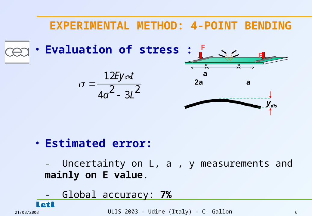
• Evaluation of stress :
• Estimated error:
- Uncertainty on L, a , y measurements and mainly on E value.
- Global accuracy: 7%
a 2a a
F F
EXPERIMENTAL METHOD: 4-POINT BENDING
21/03/2003 ULIS 2003 - Udine (Italy) - C. Gallon 7
Micrometer screw
EXPERIMENTAL METHOD: 4-POINT BENDING
a a2a
L
2aa a
L
compressive
tensile

21/03/2003 ULIS 2003 - Udine (Italy) - C. Gallon 8
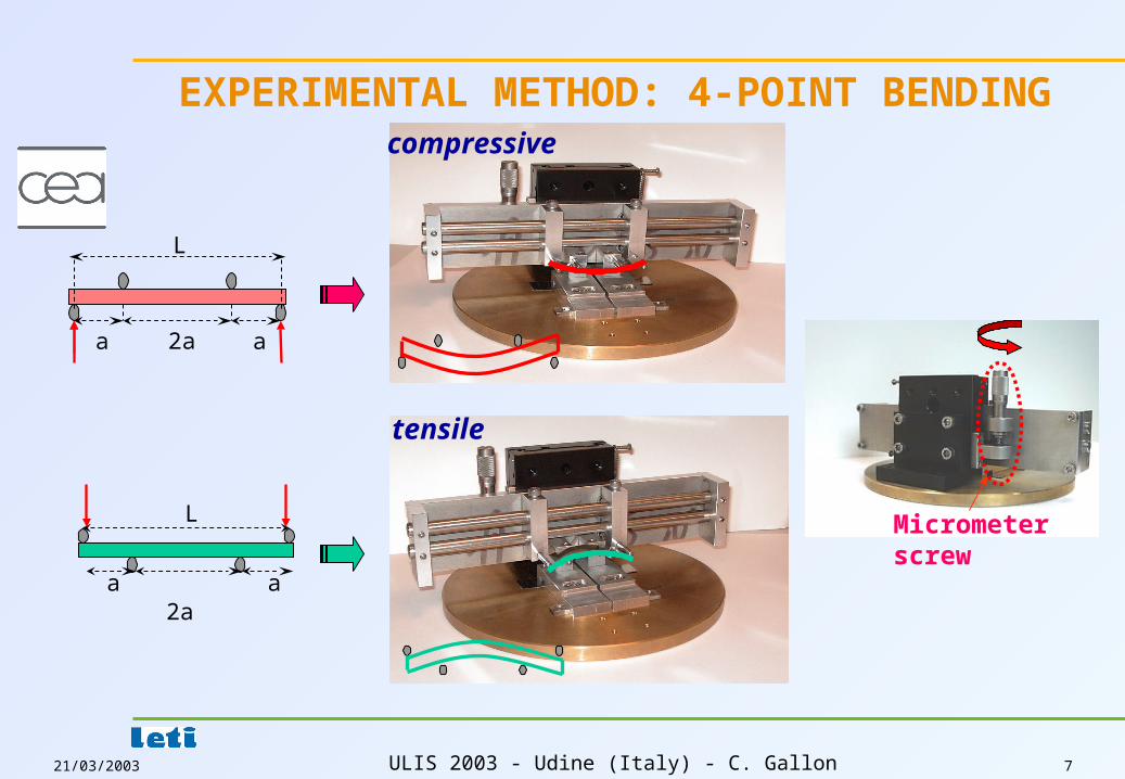
• Specific characteristics:
– Rectangular strip are cut from a saw technique.
– With an appropriate preparation of the strips, mechanical stress:
longitudinal direction (// to current flow)
or transversal direction ( to current flow).
– Most strips fail for 150-200MPa
Keep the applied mechanical stress below 100MPa.
EXPERIMENTAL METHOD: 4-POINT BENDING

21/03/2003 ULIS 2003 - Udine (Italy) - C. Gallon 9
• Bulk and SOI similar technologies- nMOS and pMOS fabricated on (100) substrates
- Tox=2nm; W=10µm; Long (L=10µm) or short (L=0.13µm) channel length;
- Important point on our short devices: a long distance between STI and gate
limit parasitic internal stress.
- Mechanical stress ranging from 0 to 100MPa was applied.
DEVICES TESTED ON 4-POINT BENDING
Substrate
Gate
DrainSource
Bulk Technology
Buried oxide
Substrate
Gate
DrainSource
SOI technology
21/03/2003 ULIS 2003 - Udine (Italy) - C. Gallon 10
EXPERIMENTAL RESULTS: Long Channel Devices
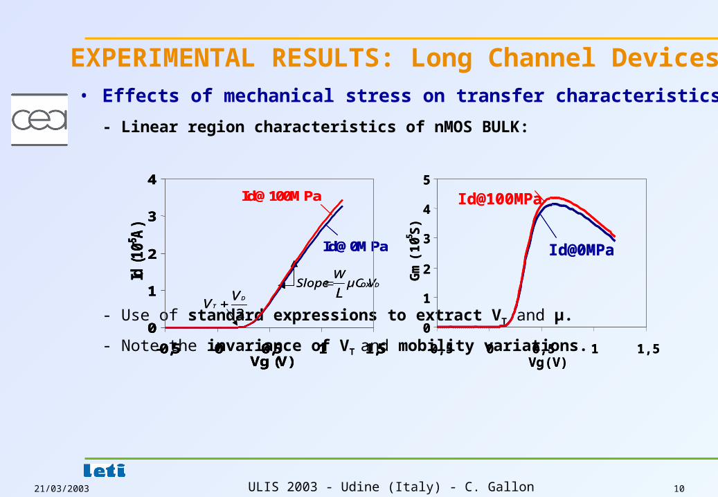
• Effects of mechanical stress on transfer characteristics
- Linear region characteristics of nMOS BULK:
- Use of standard expressions to extract VT and µ.
- Note the invariance of VT and mobility variations.
0
1
2
3
4
5
-0,5 0 0,5 1 1,5Vg (V)
Gm
(10-5
S)
Id@100MPa
Id@0MPa
0
1
2
3
4
5
-0,5 0 0,5 1 1,5Vg (V)
Gm
(10-5
S)
Id@100MPa
Id@0MPaId@0MPa
Id@100MPa
DVµCW
Slope oxL
2
D
T
VV
0
1
2
3
4
-0,5 0 0,5 1 1,5Vg (V)
Id (
10-5
A)
Id@0MPa
Id@100MPa
DVµCW
Slope oxL
2
D
T
VV
0
1
2
3
4
-0,5 0 0,5 1 1,5Vg (V)
Id (
10-5
A)
0
1
2
3
4
-0,5 0 0,5 1 1,5Vg (V)
Id (
10-5
A)

21/03/2003 ULIS 2003 - Udine (Italy) - C. Gallon 11
• Normalized mobility variations versus applied stress:
- Excellent linear dependence for both n and p MOS devices.
0
1
2
3
4
5
6
7
8
0 25 50 75 100Transversal
Longitudinal
SOI
BULK
nMOS
L=10µm W=10µm
0
1
2
3
4
5
6
7
8
0 25 50 75 100
SOI
BULK
0
1
2
3
4
5
6
7
8
0 25 50 75 1000
1
2
3
4
5
6
7
8
0 25 50 75 100Tensile Stress (MPa)
µ/µ
(%
)
-8
-202468
0 25 50 75 100
Longitudinal
SOI
02468
0 25 50 75 100
-6
02468
0 25 50 75 100
-4
02468
0 25 50 75 100
Transversal
pMOS
L=10µm W=10µm BULK
BULK
SOI
µ/µ
(%
)Tensile Stress (MPa)
EXPERIMENTAL RESULTS: Long Channel Devices
21/03/2003 ULIS 2003 - Udine (Italy) - C. Gallon 12
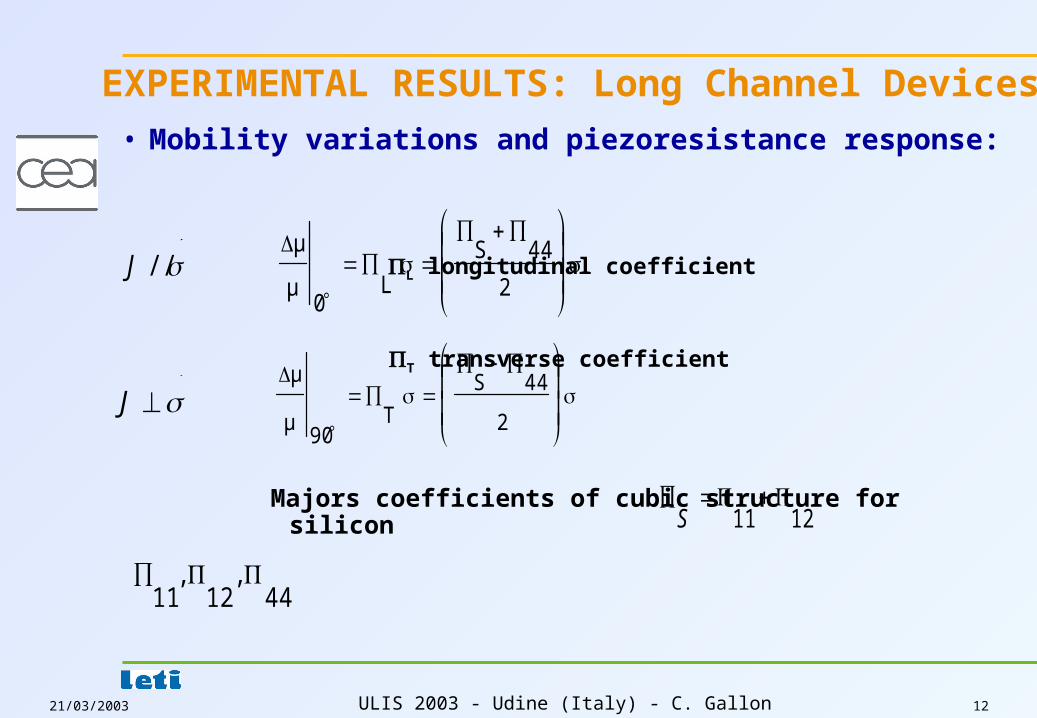
• Mobility variations and piezoresistance response:
L longitudinal coefficient
T transverse coefficient
Majors coefficients of cubic structure for silicon
2
44S
L0
µ
µ
2
44S
T90
µ
µ
//J
J
44,
12,
11
1211
S
EXPERIMENTAL RESULTS: Long Channel Devices
21/03/2003 ULIS 2003 - Udine (Italy) - C. Gallon 13
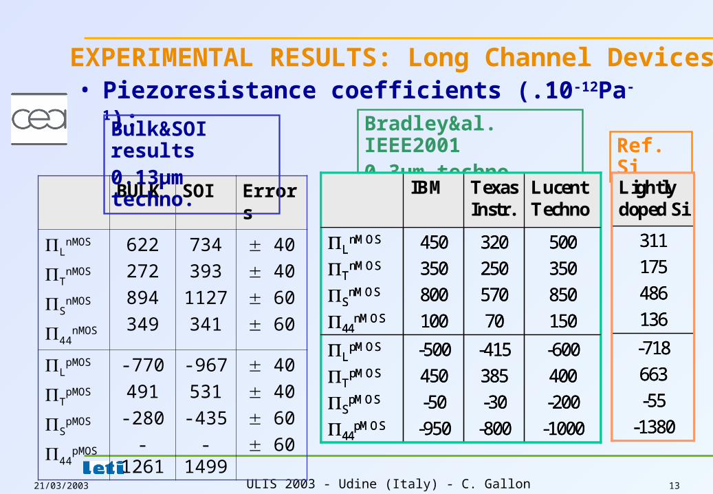
• Piezoresistance coefficients (.10-12Pa-1):
BULK SOI Errors
LnMOS
TnMOS
SnMOS
44nMOS
622
272
894
349
734
393
1127
341
40
40
60
60
LpMOS
TpMOS
SpMOS
44pMOS
-770
491
-280
-1261
-967
531
-435
-1499
40
40
60
60
Bulk&SOI results0.13µm techno.
EXPERIMENTAL RESULTS: Long Channel Devices
Bradley&al. IEEE20010.3µm techno. Ref. Si
-415
385
-30
-800
320
250
570
70
Texas Instr.
-600
400
-200
-1000
-500
450
-50
-950
LpMOS
TpMOS
SpMOS
44pMOS
500
350
850
150
450
350
800
100
LnMOS
TnMOS
SnMOS
44nMOS
Lucent Techno
IBM
-415
385
-30
-800
320
250
570
70
Texas Instr.
-600
400
-200
-1000
-500
450
-50
-950
LpMOS
TpMOS
SpMOS
44pMOS
500
350
850
150
450
350
800
100
LnMOS
TnMOS
SnMOS
44nMOS
Lucent Techno
IBM
-718
663
-55
-1380
311
175
486
136
Lightly doped Si
-718
663
-55
-1380
311
175
486
136
Lightly doped Si

21/03/2003 ULIS 2003 - Udine (Italy) - C. Gallon 14
EXPERIMENTAL RESULTS: Long&Short Channel Devices
0
2
4
6
8
0 25 50 75 100
Tensile Stress (MPa)
µ/µ
(%
)
L=0.13µm
L=10µm
nMOS
Longitudinal StressD’
S’
D
S
R
R
G
D’
S’
D
S
R
R
G
• Comparison between Long and Short devices:
Bradley&al.: “Reduction is only due to the influence of Rsd". (IEEE 2001)

21/03/2003 ULIS 2003 - Udine (Italy) - C. Gallon 15
• Bradley approach:
• Problems of this approach:
- Extraction of Ron is Vg dependent
- Choice in Vg extraction results in significant variation on Ron
Significant uncertainty on piezoresistive coefficients.
• A novel approach is proposed.
onsd
onsdeff RR
RR
21
21
EXPERIMENTAL RESULTS: Short Channel Devices

21/03/2003 ULIS 2003 - Udine (Italy) - C. Gallon 16
• New approach proposed:
1. Correction from Rsd influence on Id0:
2. Calculation of equivalent Vg shift to get the same Id with and without stress:
3. Vg is related to Vt and mobility change by:
Vd/IdR1
1IdId
0sd0
Gm/)stressed
Idunstressed
Id(Gm/IdVg
0µ/0µGm
IdVtVg [Roux-dit-Buisson,
IEEProceedings-G, 1993]
EXPERIMENTAL RESULTS: Short Channel Devices

21/03/2003 ULIS 2003 - Udine (Italy) - C. Gallon 17
1. Experimental variations after various stress levels for a 0.13µm pMOS/SOI.
Note excellent linearity.
0 0,1 0,2 0,3 0,4 0,5 0,6
100MPa
75MPa
50MPa
25MPa
0
1
2
3
4
5
0 0,1 0,2 0,3 0,4 0,5 0,6
Vg=
Id
/Gm
(10
-2V
)
Id/Gm (V)
µµSlope /
0 TV
3. Piezoresistive coefficients extraction.
EXPERIMENTAL RESULTS: Short Channel Devices
Longitudinal
Transversal02468
0 25 50 75 100
02468
0 25 50 75 100
No Rsd CorrectionRsd correction
- 2- 4- 6
- 8
Tensile Stress (MPa)µ
/µ (
%)
2. Normalized mobility change versus applied uniaxial stress.
21/03/2003 ULIS 2003 - Udine (Italy) - C. Gallon 18
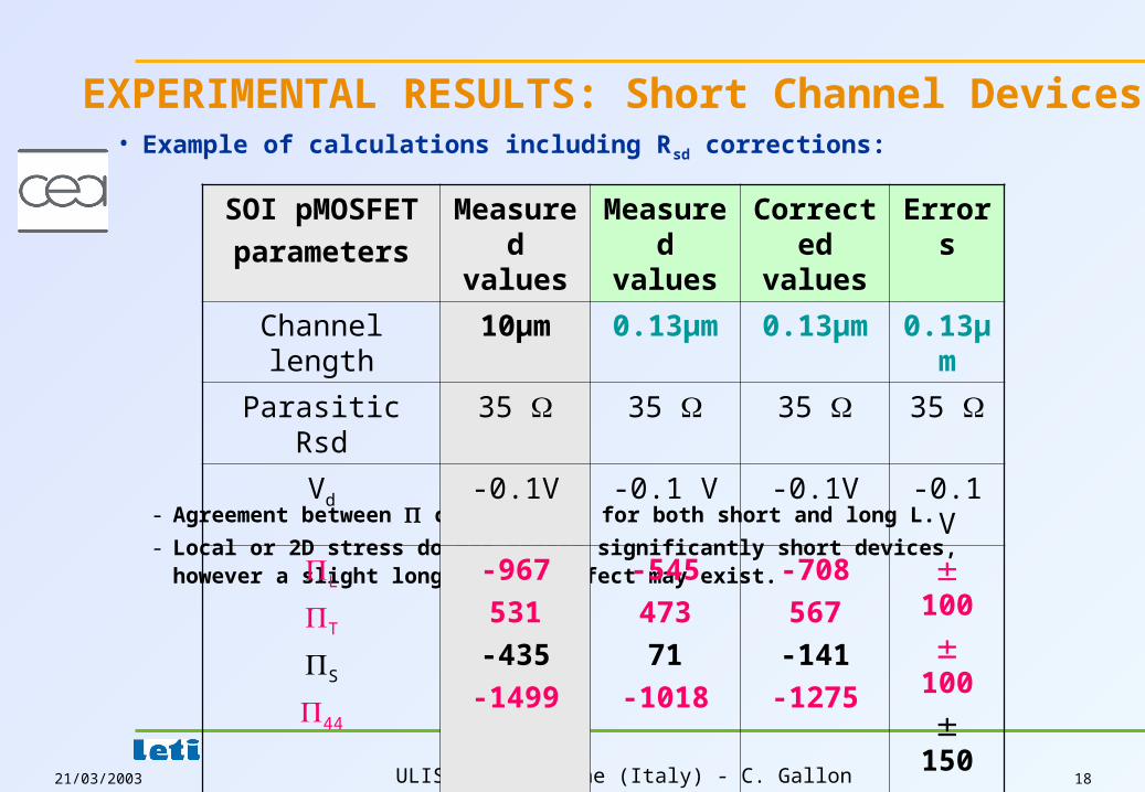
• Example of calculations including Rsd corrections:
- Agreement between coefficients for both short and long L.
- Local or 2D stress do not affect significantly short devices,however a slight longitudinal effect may exist.
SOI pMOSFET
parameters
Measured values
Measured values
Corrected values
Errors
Channel length 10µm 0.13µm 0.13µm 0.13µm
Parasitic Rsd 35 35 35 35
Vd -0.1V -0.1 V -0.1V -0.1 V
L
T
S
44
-967
531
-435
-1499
-545
473
71
-1018
-708
567
-141
-1275
100
100
150
150
EXPERIMENTAL RESULTS: Short Channel Devices

21/03/2003 ULIS 2003 - Udine (Italy) - C. Gallon 19
CONCLUSIONS & PERSPECTIVES
• Study of mechanical stress effects on long and short channels.
• Proposition of a simple approach to determine directly Vt and µ
– Vt is independent of stress,
– Mobility variations dominate the piezoresistive response,
– Bulk & SOI: similar piezoresistive response both n and p MOS, slightly higher for SOI.
• After Rsd corrections, comparable results on short and long devices:
2D or local effects are small for a 0.13µm technology.
• A first step to provide piezoresistive data for device simulators and a better analysis of mechanical stress effects.