2011 gcep report - stanford university · 2011 gcep report project title ... potential improvement...
TRANSCRIPT
2011 GCEP Report
Project title: Advanced electron transport materials for application in organic photovoltaics (OPV)
Investigators Michael McGehee, Associate Professor, Materials Science and Engineering Alan Sellinger, Senior Research Scientist/Consulting Associate Professor, Materials Science and Engineering Andrew Higgs, Tommaso Giovenzana – Post Doctoral Researchers; Jason Bloking – Graduate Researcher; Jack Kastrop - Undergraduate Researcher Timeframe of research - September 2010-March 2011 Abstract
This project is focused on discovering efficient, less expensive and tunable organic-based electron transport materials for application in organic photovoltaics (OPV) in an effort to replace more commonly used fullerene-based materials. The emphasis during the first six months of this project was more on the synthesis of new materials, with less emphasis on device fabrication that will ramp up during the next stage. Several novel molecules were designed, prepared and characterized from simple, minimal step, moderate yield, and inexpensive synthetic processes. These novel materials were prepared by chemically linking together conjugated electron deficient moieties of phenyl- and naphthyl-imides, dicyanoimidazoles and benzothiadiazoles. Initial thermal, optical and electronic characterization of these materials suggests they have favorable properties such as relatively high-temperature thermal transitions, favorably-located energy levels, visible light absorption, high solubility in commonly used organic solvents, and high purity. For example, they are excellent candidates to prepare solution processed bulk heterojunction (BHJ) OPVs by combining with regio-regular poly(3-hexylthiophene), the most commonly studied donor material used in bulk heterojunction OPVs.
Introduction & Background
Organic photovoltaics (OPV) have recently reached power conversion efficiencies (PCE) of 8.3%1 and extrapolated lifetimes of >30 years2 bringing this area of technology closer to commercialization. Common to both of these reports are the use of fullerenes as
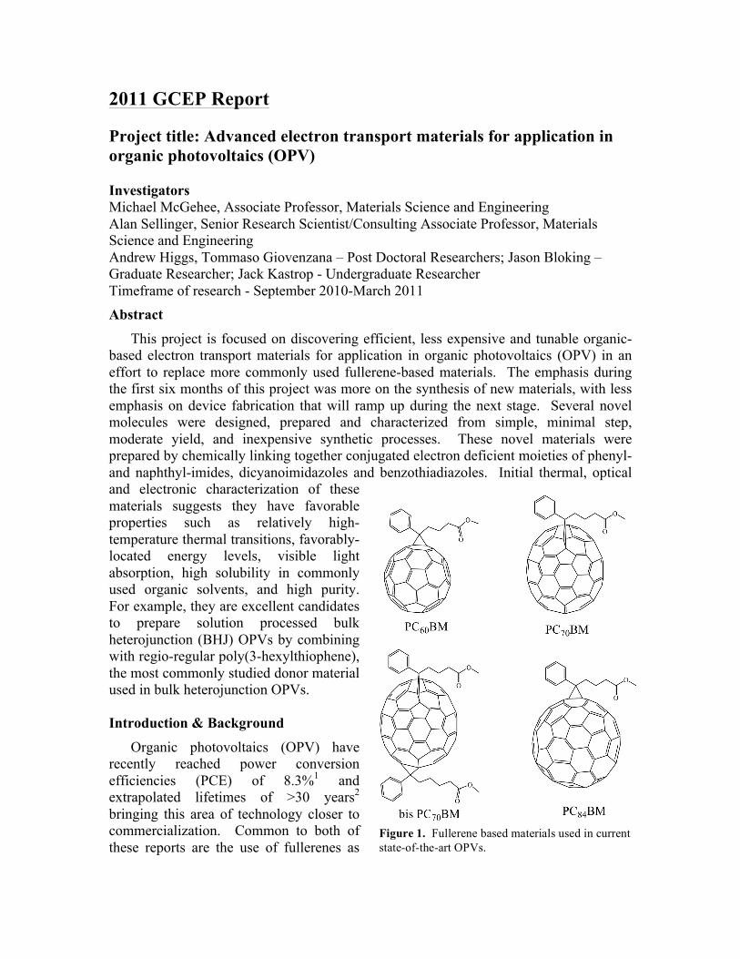
Figure 1. Fullerene based materials used in current state-of-the-art OPVs.

the electron acceptor/transport materials. In the case of Chen et al,3 bulk heterojunction (BHJ) solar cells are reported where PC70BM (Figure 1) is used as the acceptor together with a novel donor polymer. For the report by Schwartz et al,2 vacuum deposited tandem devices are prepared using the “naked” C60 molecule as the acceptor with small molecule donor materials. Despite these exciting developments for OPVs, from a materials perspective fullerenes tend to have low absorption in the visible range, produce devices with relatively low open circuit voltages (Voc), and are very difficult to synthesize and purify, which leads to higher costs. The most commonly used fullerene compounds for solution processed OPVs are shown in Figure 1. These compounds are functionalized with side chains that make them more soluble for solution processing. Of the fullerene derivatives in Figure 1, PC60BM is the most commonly used primarily because it is the least expensive ($300/g). PC70BM, PC84BM, and bis-PC70BM have been recently shown to improve device performance, but the higher prices for these materials, $800/g, $10,000/g, and $1200/g respectively, ultimately translates into higher cost OPV cells.
With regard to new materials development for application in OPVs, to date most studies have focused on electron donor semiconductors,4 with significantly less work being reported on new electron acceptor materials. New acceptor materials that could address and solve the issues of fullerenes described above could push PCE levels to 10% or higher and reduce the cost. For example, replacing the weakly absorbing fullerenes with more strongly absorbing acceptors should lead to efficient light harvesting below 700nm (Figure 2a) and increased short circuit current densities (Jsc). Assuming a peak external quantum efficiency (EQE) of 0.75, we estimate the Jsc can be improved from 15.2 mA/cm2 in the record device3 to 17.2 mA/cm2 (Figure 3).
Even in optimized state-of-the-art devices, a significant fraction of the incident power is lost due to the large offset in the HOMO and LUMO levels between the two materials (Figure 2b). It has been shown that with properly chosen electrodes, the difference in energy between the HOMO of the donor and the LUMO of the acceptor is typically 0.3V larger than the Voc of the device. Although a HOMO level offset (and LUMO level offset) of about 0.3V is required to split the photogenerated excitons,5 a large HOMO and
(a) (b) Figure 2. (a). Potential improvement in EQE over the current record device from using new acceptor materials. (b) Energy levels in the record bulk heterojunction solar cell between the donor polymer PBDTTT-CF and the fullerene acceptor PCBM.3

LUMO offset results in a reduction in the Voc that the device can produce. If new acceptor materials can be designed with HOMO and LUMO levels that are less electronegative (red arrows in Figure 2b), the reduced HOMO and LUMO offsets would result in higher Voc. Assuming that Voc = ELUMO,Acceptor –EHOMO,Donor – 0.3V, reducing the HOMO and LUMO energy offsets to 0.3V would increase the Voc of this device to 1.2V (Figure 3).
Fill factors of 0.7 have been obtained in the commonly studied system of regio-regular poly(3-hexylthiophene) (P3HT) with PC60BM BHJ devices and should also be attainable in devices with new acceptors that have electron mobilites comparable to the fullerenes. Assuming a fill factor of 0.7, the improvements in the Voc (1.2V) and Jsc (17.2 mA/cm2) would result in a 14.4% efficient device.
Of the few non-fullerene acceptor materials that have been reported in the literature, perylene derivatives, cyano poly(phenylenevinylenes) (CN-PPV), and 4,5-dicyanoimidazole (VinazeneTM) based materials have been the most promising, resulting in top PCEs of ~2% when combined with a donor material.6 As the potential for PCEs greater than 10% is a reality, there needs to be a systematic fundamental study on new acceptor materials for application in OPVs that includes chemical synthesis, materials characterization, and device physics.
Results 1. Design of new acceptors
Examples of the most promising non-fullerene acceptors for application in OPVs have been recently reported and reviewed.7-17 We first reported the synthesis and characterization of a series of n-type conjugated materials based on the Heck reaction of 4,5-dicyano-2-vinylimidazole (VinazeneTM) with selected dibromoaromatics.12, 18 These materials were easily prepared with high yields from one-step reactions using commercially available materials. The most promising material from these studies was 4,7-bis(2-(1-(2-ethylhexyl)-4,5-dicyanoimidazol-2-yl)vinyl)benzo[c][1,2,5]-thiadiazole (EV-BT, where EV is ethylhexylvinazene and BT is benzothiadiazole) shown in Figure 4. EV-BT, with its favorable solid-state electron affinity (3.5 eV) and absorption in the visible spectrum
Figure 3. Potential improvement in the current-voltage characteristics from using new acceptor materials.
Figure 4. 4,7-bis(2-(1-(2-ethylhexyl)-4,5-dicyanoimidazol-2-yl)vinyl)benzo[c][1,2,5]-thiadiazole (EV-BT). Used in BHJ devices with selected donor polymers to make OPVs with Voc up to 1.4V and PCEs of 1.4%.

produced, with selected donor polymers, OPVs with Voc up to 1.4 V and PCEs of 1.4%, some of the highest values reported for non-fullerene acceptors.6, 13 We suspect the lower fill factor (FF) and short-circuit current of these devices (50% and 5.7 mA/cm2) compared to P3HT:PC61BM (67% and ~10 mA/cm2) can be partially attributed to the low electron mobility of EV-BT [10-5 cm2/V-s, as measured by space charge limited current (SCLC) methods] compared to PC61BM (10-3 cm2/V-s).19 We propose that the low electron mobility of this acceptor may be due to the asymmetric alkyl-chain direction on the vinyldicyanoimidazole moiety preventing efficient p-p molecular stacking. Figure 5 shows how the placement of the alkyl chains could be controlled to create more
symmetrical molecules that are proposed to enhance p-p molecular stacking leading to better electron mobility.
To synthetically prepare molecules and achieve this objective, we proposed the introduction of electron deficient arylvinyl imide units on the central benzothiadiazole
Figure 6. Prepared molecules leading to enhanced π−π molecular stacking that may lead to better electron mobility.
Figure 5. Schematic showing the proposed structure/property relationships leading to enhanced π−π molecular stacking that may lead to better electron mobility.

moiety where a more symmetric placement of the alkyl chains at the ends of the molecule could be positioned, as shown in Figure 6 (PI-BT, NI-BT, PI-PI and NI-PI) where PI is phenylimide and NI is naphthylimide. In the case of PI-PI and NI-PI we also introduce alkyl chains on the central moiety for enhanced solubility. Furthermore, the molecules were designed with extended π-conjugated systems that help contribute to absorption of visible light, and tunable chemistry to allow for varying of the ionization potential, electron affinity, and solubility.13 Initial quantum-chemical calculations using density functional theory (DFT) of methyl analogs (performed by Prof. Jean-Luc Bredas’ group at Georgia Tech) show that PI-BT, and other analogues with the Vinazene (EV) and phenylimide moiety (PI), maintains a planar geometry in the ground-state that, together with the position of the alkyl chains, will favor efficient π−π stacking of the acceptor molecules and hopefully enhance the electron mobility in the π−π direction. However, in the case of NI-BT, steric interactions between neighboring hydrogen atoms in the naphthyl and vinyl moieties induce a 27.3º twisting in the ground-state (Figure 7). This twisting may prohibit efficient packing and crystal formation between neighboring molecules lowering the electron mobility in NI-BT compared with PI-BT.
1.1 Synthesis of new acceptors
The synthesis of the five new non-fullerene based molecules are shown in Scheme 1. The new molecules were synthesized through the Heck coupling reaction in toluene.10, 15,
16 These five new acceptors, BV-PI, PI-BT, NI-BT, PI-PI, and NI-PI are composed of an “A” building block (benzothiadizole or phthalimide based compounds) and two “B” building blocks (imide or vinazene bearing compounds) as shown in Scheme 1. The Heck coupling reaction is a commonly used oxidative coupling that forms conjugated C-
Figure 7. Molecular structure and ground-state geometries of EV-BT, PI-BT and NI-BT.
C bonds between vinyl and aromatic compounds. The catalyst used was primarily bis(tri-tert-butylphosphine)palladium(0) (Pd[P(tBu)3]2). For the Heck coupling reactions using Pd[P(tBu)3]2 as catalyst, dicyclohexylmethylamine (Cy2NMe) was added as base/HBr scavenger. The ligand tri-o-tolylphosphine (P(o-tol)3) was also used for the synthesis of PI-BT and NI-BT. BV-PI was synthesized directly from the starting materials of DiCl-Ph-Im and butylvinazene. PI-BT and NI-BT were synthesized via the intermediate, BTSi, and Br-Ph-Im and Br-N-Im, respectively with DiBr-BT as the central moiety. PI-PI and NI-PI were synthesized via the intermediate, PISi, and Br-Ph-Im and Br-N-Im, respectively. The overall yields of these n-type acceptor molecules are in the range of 20-70 %. Since the synthesis of PI-BT, NI-BT, PI-PI, and NI-PI involve two-step reactions the yields for PI-BT, NI-BT, PI-PI, and NI-PI (20-50%) were lower than the yield for BV-PI (66%).
1.2 Materials Characterization
1.2.1 Nuclear magnetic resonance (NMR), elemental analysis (EA) and mass spectrometry (MS)
Scheme 1. Synthetic procedures for intermediates and final acceptor molecules to be used for application in OPVs.

A detailed experimental procedure is described for each intermediate and final compound and is available upon request. As an example, we highlight the procedure with corresponding characterization results for PI-BT below. Synthesis of 4,7-bis(4-(N-hexyl-phthalimide)vinyl)benzo[c]1,2,5-thiadizole (PI-BT).
To a Schlenk flask were added BTSi (0.80 g, 1.56 mmol), Br-Ph-Im (1.06 g, 3.43 mmol), Pd(dba)2 (90 mg, 0.16 mmol), and ligand (P(o-tol)3, 142 mg, 0.47 mmol). The flask was evacuated, and then refilled with N2 three times. Toluene (25 mL) was added and the reaction mixture was stirred at 80oC for 20 min. Then tetrabutyl ammonium fluoride (TBAF) (3.7 mL, 1.0 M in THF) was added and the reaction mixture was stirred at 80oC for 2 days. The solution was extracted with water and CH2Cl2 three times and dried over magnesium sulfate. The compound was purified by column chromatography in silica gel using CH2Cl2. Precipitation was done in methanol and the red color solid 0.49 g (49 % yield) were collected by vacuum filtration and dried overnight. 1H NMR (300 MHz, CDCl3): δ 0.89 (t, 6H), 1.33 (m, 12H), 1.71 (qui, 4H), 3.70 (t, 4H), 7.75 (d, 2H), 7.79 (s, 2H), 7.86 (d, 2H), 7.89 (d, 2H), 8.14 (s, 2H), 8.24 (d, 2H). 13C NMR (100 MHz, CDCl3): δ 14.02, 22.52, 26.55, 28.58, 31.37, 38.18, 120.51, 123.66, 128.20, 128.53, 129.26, 130.85, 132.07, 133.03, 143.46, 153.65, 168.13, 168.31. C38H38N4O4S (646.80): Calcd. C 70.56, H 5.92, N 8.66, S 4.96; Found C 69.38, H 5.67, N 8.40, S 4.89.
1.2.2. Opto-electronic and thermal characterization EV-BT, BV-PI, PI-BT, NI-BT, PI-PI and NI-PI were characterized using ultraviolet-
visible (UV-Vis) spectroscopy, photoluminescence (PL) spectroscopy, photo-electron spectroscopy in the air (PESA), thermal gravimetric analysis (TGA), and differential scanning calorimetry (DSC) and the results are reported in Table 1.
Table 1. Optical, Electrical, and Thermal Properties of the New Acceptor Molecules.
Compound UV-Vis (nm) in
THF
PL (nm) in THF Eg
a (eV) HOMOb/LUMOa (eV)
Melting Point (°C)
Extinction Coefficient (M-1cm-1)
EV-BT 335, 442 516 2.43 5.91/3.51 205 3.33 E+05 BV-PI 375 444 2.70 5.90/3.20 220 1.92E+05 PI-BT 448 525 2.34 6.06/3.72 156 2.29 E+05 NI-BT 467 547 2.16 5.98/3.82 241 3.85 E+05 PI-PI 385 454 2.58 5.93/3.35 - 4.74E+05 NI-PI 415 480 2.53 5.78/3.25 195 2.93E+05 aDetermined from UV onset. bDetermined from PESA.
Example absorption and emission spectra for selected molecules (PI-BT and PI-PI)
are shown in Figure 8. EV-BT and BV-PI are the two acceptors bearing vinazene units for the “B” building block. EV-BT has two main absorption peaks at 335 and 442 nm. The lower wavelength main absorption peak originates from the vinazene unit. However, BV-PI has only one absorption peak with the maximum absorption wavelength (λmax) at 375 nm. This might be due to the shorter conjugation length introduced by the phthalimide unit than the benzothiadiazole unit. A red-shifted absorption onset value of EV-BT (510 nm) is also found compared with BV-PI (460 nm). The bandgap of EV-BT (2.43 eV) is lower than that of BV-PI (2.70 eV). Therefore, the bandgap of the acceptor

molecule can be tuned by using various “A” building blocks with different π-conjugation systems. λmax of PI-BT and NI-BT, which contain the same “A” building block (benzothiadizole), but different imide-based “B” building blocks, are 448 and 467 nm, respectively. The absorption onset value of NI-BT (620 nm) is red-shifted by 90 nm compared to PI-BT (530 nm) due to the extended conjugation of the naphthalimide unit of the “B” building block. Similarly, λmax of PI-PI and NI-PI, which contain the same “A” building block (phthalimide), but different imide-based “B” building blocks, are 385 and 415 nm, respectively. The absorption onset value of NI-PI (490 nm) is red-shifted by 10 nm compared to PI-PI (480 nm) due to the extended conjugation of the naphthalimide unit of the “B” building block. Thus, the bandgap of the acceptor can be tuned by using different “B” building blocks as well. Comparing the optical properties of the four new acceptor molecules reveals that by changing the “A” and “B” building blocks of the acceptor, one can tune the molecule’s bandgap to optimize the absorption properties.
Figure 8. Representative UV-Vis and PL spectra of PI-BTand PI-PI in THF solution.
The maximum emission wavelengths of EV-BT, BV-PI, PI-BT, NI-BT, PI-PI, and
NI-PI in solution are at 516, 444, 525, 547, 454, and 480 nm, respectively. λmax of EV-BT, NI-BT, and NI-PI are red-shifted compared to those of BV-PI, PI-BT and PI-PI. The absorption coefficients shown in Table 1 are measured by varying the acceptor molecule solution concentration and examining the change in intensity of their λmax. The values of the absorption coefficients are measured in the range of 1.9-3.9×10⁵ M-1cm-1, indicating that the molecules have strong absorption in the visible spectrum, which is promising and desirable for photocurrent generation in OPVs.
The HOMO levels of the acceptor as measured by PESA are in the range of 5.8-6.1 eV, also shown in Table 1. The bandgaps (2.2-2.7 eV) of the acceptors are estimated from the UV-Vis onset. The LUMO levels (3.2-3.8 eV) are calculated based on the bandgaps and the HOMO levels. Based on the results thus far, all of these molecules have favorable energy levels to act as electron acceptor materials when combined with common electron donor materials such as poly-(3-hexythiophene) (P3HT). The calculated and the experimental values of HOMO/LUMO and bandgaps of acceptor materials, EV-BT, PI-BT, NI-BT, PI-PI, and NI-PI, are listed in Table 2.

Table 2. Calculated vs. experimental HOMO/LUMO and bandgaps of acceptor materials.
Compound Calculated Eg (eV)
Experimental Eg (eV)
Calculated HOMO/LUMO
(eV)
Experimental HOMO/LUMO
(eV) EV-BT 2.63 2.43 6.29/3.65 5.91/3.51 PI-BT 2.61 2.34 5.76/3.15 6.06/3.72 NI-BT 2.50 2.16 5.77/3.27 5.98/3.82 PI-PI 3.15 2.58 6.03/2.89 5.93/3.35 NI-PI 2.93 2.53 5.98/3.05 5.78/3.25
The difference of the calculated and the experimental bandgap values are in the range
of 0.2-0.4 eV. The difference of the calculated and the experimental HOMO and LUMO values are in the range of 0.1-0.4 eV and 0.1-0.5 eV, respectively. Thus, the molecular modeling trends (performed by the Bredas group at Georgia Tech) are consistent with the experimental results and can be a valuable tool when designing new molecules.
Figure 9 shows images of the acceptors, EV-BT, BV-PI, PI-BT, NI-BT, PI-PI, and NI-PI in solution (THF) under visible and ultraviolet light, respectively. The intense PL emission is a valuable property as we will later perform PL quenching studies when combining these materials with selected donors, to examine exiton splitting efficiency.
Figure 9. EV-BT, BV-PI, PI-BT, NI-BT, PI-PI, and NI-PI in solution (THF) under visible and ultraviolet light.
The thermal properties of the small molecule acceptors were investigated by thermogravimetric analysis (TGA) and differential scanning calorimetry (DSC). All molecules showed high decomposition temperatures (Td > 360°C) indicating these acceptors have good thermal stability. The melting points of these acceptors in the range of 150-285°C are measured using DSC and are shown in Table 1. The relatively high melting points of EV-BT, BV-PI, PI-BT, NI-BT, and NI-PI indicate the temperature limits of thermal annealing during processing. 1.2.3 Space-charge limited current (SCLC)
Electron-only devices of pure films were prepared to measure the electron mobility of various acceptor materials, via the space-charge limited current (SCLC) technique. Electron-selective contacts of low work-function metals and inorganic materials such as Al2O3/Al (work function (Φ) ~ 4.0-4.3 eV), Cs2CO3/Al (Φ ~ 2.1 eV), Ca/Al (Φ ~ 2.9 eV),
EV-BT, BV-PI, PI-BT, NI-BT, PI-PI, NI-PI EV-BT, BV-PI, PI-BT, NI-BT, PI-PI, NI-PI
(a) Acceptors (in THF) under visible light (b) Acceptors (in THF) under UV light

and LiF/Al (Φ ~ 2.7 eV) have been used. Electron-only contacts have been known to suffer from stability issues, leading to observation of nonlinear differential resistances.20 The majority of our devices synthesized using these contacts also display the nonlinear resistances, in addition to I-V curves dependent upon the type of contacts used, which prevents accurate fitting of data to space-charge current models. Further investigation is planned with other electron-only contacts, Ba/Al (Φ ~ 2.7 eV) and Sm/Al (Φ ~ 2.7 eV). Both these contacts have been shown to provide more reliable data in measuring electron mobility with other n-type organic semiconductors.21 2. Organic photovoltaics incorporating new acceptors
Selected acceptor molecules described above have been incorporated into BHJ devices using P3HT as donor material. Based on their low-lying LUMO levels and high absorption coefficients, PI-BT and NI-BT were selected as initial materials for investigating the photovoltaic performance. Energy band diagrams with P3HT for each device are shown in Figure 10, indicating that the LUMO-LUMO offset between the donor and acceptor should be sufficient to drive exciton splitting at the interface, while also providing for large open-circuit voltages depending on the difference between the donor HOMO and the acceptor LUMO.
Figure 10. Energy level diagram for devices with P3HT as donor and PI-BT and NI-BT as acceptor.
Photovoltaic devices using the new acceptor molecules were prepared by spinning
solutions of P3HT and the acceptor in an organic solvent (chloroform, toluene, chlorobenzene or 1,2-dichlorobenzene) onto pre-cleaned patterned substrates of indium tin oxide (ITO) on glass, further coated with a thin layer of poly (3,4-ethylenedioxythiophene) poly(styrenesulfonate) (PEDOT:PSS). The active layer was allowed to dry before further annealing treatments. Cathodes were thermally evaporated at less than 10-6 Torr before testing. All steps following coating with PEDOT:PSS including device testing were performed in a dry nitrogen-atmosphere glovebox. Testing of the devices was performed under 100 mW/cm2 calibrated illumination with an AM1.5G spectrum.
J-V curves for the most efficient devices prepared from blends of P3HT and PI-BT dissolved in chloroform are shown in Figure 11a. The current is below the 10 mA/cm2,
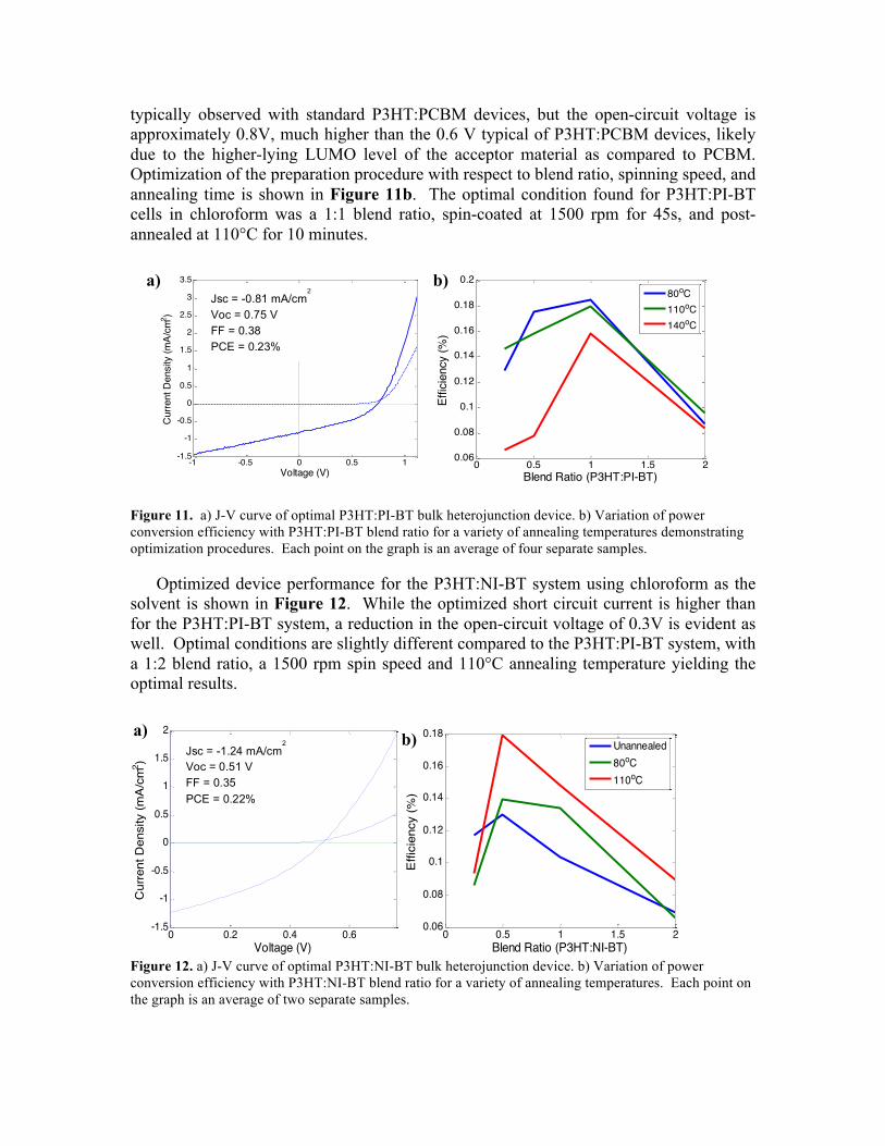
typically observed with standard P3HT:PCBM devices, but the open-circuit voltage is approximately 0.8V, much higher than the 0.6 V typical of P3HT:PCBM devices, likely due to the higher-lying LUMO level of the acceptor material as compared to PCBM. Optimization of the preparation procedure with respect to blend ratio, spinning speed, and annealing time is shown in Figure 11b. The optimal condition found for P3HT:PI-BT cells in chloroform was a 1:1 blend ratio, spin-coated at 1500 rpm for 45s, and post-annealed at 110°C for 10 minutes.
Figure 11. a) J-V curve of optimal P3HT:PI-BT bulk heterojunction device. b) Variation of power conversion efficiency with P3HT:PI-BT blend ratio for a variety of annealing temperatures demonstrating optimization procedures. Each point on the graph is an average of four separate samples.
Optimized device performance for the P3HT:NI-BT system using chloroform as the
solvent is shown in Figure 12. While the optimized short circuit current is higher than for the P3HT:PI-BT system, a reduction in the open-circuit voltage of 0.3V is evident as well. Optimal conditions are slightly different compared to the P3HT:PI-BT system, with a 1:2 blend ratio, a 1500 rpm spin speed and 110°C annealing temperature yielding the optimal results.
Figure 12. a) J-V curve of optimal P3HT:NI-BT bulk heterojunction device. b) Variation of power conversion efficiency with P3HT:NI-BT blend ratio for a variety of annealing temperatures. Each point on the graph is an average of two separate samples.
-1 -0.5 0 0.5 1-1.5
-1
-0.5
0
0.5
1
1.5
2
2.5
3
3.5
Cur
rent
Den
sity
(mA/
cm2 )
Voltage (V)
Jsc = -0.81 mA/cm2
Voc = 0.75 VFF = 0.38PCE = 0.23%
0 0.5 1 1.5 20.06
0.08
0.1
0.12
0.14
0.16
0.18
0.2
Blend Ratio (P3HT:PI-BT)
Effic
ienc
y (%
)
80oC110oC140oC
Jsc = -0.81 mA/cm2
Voc = 0.75 V FF = 0.38 PCE = 0.23%
0 0.2 0.4 0.6-1.5
-1
-0.5
0
0.5
1
1.5
2
Cur
rent
Den
sity
(mA
/cm
2 )
Voltage (V)
Jsc = -1.24 mA/cm2
Voc = 0.505 VFF = 0.35PCE = 0.2192%
Jsc = -1.24 mA/cm2
Voc = 0.51 V FF = 0.35 PCE = 0.22%
0 0.5 1 1.5 20.06
0.08
0.1
0.12
0.14
0.16
0.18
Blend Ratio (P3HT:NI-BT)
Effi
cien
cy (%
)
Unannealed80oC110oC
a) b)
a) b)

3. Future work Going forward we will take advantage of our chemistry/device interdisciplinary team.
For example, our device group will provide feedback for our chemists in order to make necessary changes to the molecules with regard to solubility, energy level adjustments, and absorption properties. The first planned studies will continue to evaluate the 5 molecules described above by optimizing solution processed OPVs with P3HT. We then will transition to more recently reported donor polymers such as POPT9, PQT-OP, and PCDTBT22 (Figure 13) that have outperformed P3HT with regards to fullerene and/or EV-BT based devices.
3.1 Solid-State Film Morphology As outlined in our proposal, previous studies have shown the significant effects that
solid-state organic thin film morphology can have on OPV properties, most notably charge carrier mobility and exciton quenching. Since intermolecular charge transport is accomplished via a hopping mechanism in many organic semiconductors, the electron wavefunction overlap between adjacent molecules is critical to promoting good charge transport through a film. Various aspects of the molecular structure can affect the overlap between adjacent molecular wavefunctions. To investigate this, specular grazing incidence x-ray scattering (GIXS) techniques will be used to probe the packing of acceptor molecules in the solid state. By investigating how molecular features such as alkyl chain length and orientation affect molecular packing, rational design of future molecules can further optimize packing in order to improve electron wavefunction overlap, charge transport and finally, OPV performance.
3.2. Loss Mechanisms We propose to investigate the loss mechanisms in BHJ OPVs with non-fullerene
acceptors and compare these results with fullerene devices to gain insight into what advantageous properties of fullerene molecules should be emulated in the new acceptor materials. For example, it has been proposed that the high electron mobility of fullerenes
Figure 13. Donor polymers that we plan to study with our new acceptors in future experiments.

(on the order of 10-3 cm2V-1s-1) is a reason why it outperforms other acceptor materials. However, some new acceptors with electron mobilities approaching or exceeding this value also have poor OPV performance. Morphological properties of fullerene BHJ films may also play an important role. Recently our group has shown that fullerene molecules intercalate between the side chains of many donor polymers, which may lead to improved charge separation or extraction properties of the device.23 Additional reasons have been proposed in the literature including the high dielectric constant of fullerenes (εr = 4) which may screen the attraction between geminate electron-hole pairs and reduce their rate of (geminate) recombination as well as the triply degenerate LUMO state of C60, which may enable fullerenes to better accommodate electrons. One direction that we propose to examine is how triplet states play a role in geminate electron-hole pair recombination in different blend combinations. Recently it has been shown that a significant recombination pathway in some BHJ solar cells is through triplet states in either of the materials in the blend.24 A large number of blends (~20) were investigated using materials with high absorption coefficients and mobilities. It was found that in blend combinations where the devices did not perform well, but the excitons were split (as evidenced by PL quenching), the triplet energy of the one of the materials was lower than the energy of the charge transfer state. It was suggested that in these blends, following charge transfer, back transfer can occur to the triplet state, which then recombines through radiative or non-radiative mechanisms (Figure 14).
This type of characterization has been performed on a small number of acceptors to date. We propose investigating if recombination via the triplet state is a significant loss mechanism in blends with non-fullerene acceptors. This information will be used to design new materials with raised triplet energies to examine what impact this has on this recombination pathway. We would then measure the triplet and charge transfer energies of blends with the new acceptors to determine if the triplet energies are lower and if photocurrent is being lost to triplet states. We propose using photo-thermal deflection spectroscopy to measure the weak charge transfer absorption of blends to determine the charge transfer energy.25 In this method the film is submerged in a liquid with a highly temperature sensitive dielectric constant. Weak absorptions cause the liquid to heat up, resulting in small deflections of a laser beam.
(a) (b)
Figure 14. a) Charge transfer process in a functioning device and b) Charge transfer followed by back transfer to the triplet state in a poorly performing device.

We have recently constructed a set up to measure the photo induced absorption spectra of films and solutions which can be used to measure the triplet energies of new acceptor molecules by the method of triplet sensitization/quenching.24 In this method, blend films or solutions are made of the test material with materials of known triplet energy. The test material or the standard is then excited with a laser and the presence of triplets in either material can be observed by a small change in the absorption. Triplets will transfer from the material of higher triplet energy to those of lower triplet energy, thus the triplet energy of the test material can be determined by observing on which material the triplets remain.
These studies will provide insight into geminate recombination losses in BHJ devices via triplet states. We hope to better understand the extent to which triplet energy engineering needs to be taken into account in addition to HOMO and LUMO energies in the design of new acceptor materials. Patent Disclosure 1. United States Provisional Patent Application, “Electron deficient molecules and their use in
Organic Electronic Applications”, Alan Sellinger, Xu Han, Jason Bloking and Michael D. McGehee, submitted April 4, 2011.
Publications 1. Xu Han, Jason T. Bloking, Andrew T. Higgs, Laxman Pandey, Joseph E. Norton, Chad
Risko, Cynthia E. Chen, Jean-Luc Brédas, Michael D. McGehee, and Alan Sellinger, manuscript in preparation.
References 1. Wemett, T. Konarka's Power Plastic Achieves World-Record 8.3% Efficiency Certification
from National Renewable Energy Laboratory (NREL). http://www.konarka.com/index.php/site/pressreleasedetail/konarkas_power_plastic_achieves_world_record_83_efficiency_certification_fr (January 26, 2011),
2. Schwartz, G.; Maennig, B.; Uhrich, C.; Gnehr, W.; Sonntag, S.; Erfurth, O.; Wollrab, E.; Walzer, K.; Pfeiffer, M. In Efficient and long-term stable organic vacuum deposited tandem solar cells, San Diego, CA, United states, 2009; SPIE: San Diego, CA, United states, 2009; p The International Society for Optical Engineering (SPIE).
3. Chen, H. Y.; Hou, J. H.; Zhang, S. Q.; Liang, Y. Y.; Yang, G. W.; Yang, Y.; Yu, L. P.; Wu, Y.; Li, G. Nature Photonics 2009, 3, (11), 649-653.
4. Kroon, R.; Lenes, M.; Hummelen, J. C.; Blom, P. W. M.; De Boer, B. Polymer Reviews 2008, 48, (3), 531-582.
5. Bredas, J. L.; Beljonne, D.; Coropceanu, V.; Cornil, J. Chemical Reviews 2004, 104, (11), 4971-5003.
6. Woo, C. H.; Holcombe, T. W.; Unruh, D. A.; Sellinger, A.; Frechet, J. M. J. Chemistry of Materials 2010, 22, (5), 1673-1679.
7. Brunetti, F. G.; Gong, X.; Tong, M.; Heeger, A. J.; Wudl, F. Angewandte Chemie-International Edition 49, (3), 532-536.

8. Brunetti, F. G.; Kumar, R.; Wudl, F. Journal of Materials Chemistry 20, (15), 2934-2948. 9. Holcombe, T. W.; Woo, C. H.; Kavulak, D. F. J.; Thompson, B. C.; Frechet, J. M. J. Journal
of the American Chemical Society 2009, 131, (40), 14160-+. 10. Kietzke, T.; Shin, R. Y. C.; Egbe, D. A. M.; Chen, Z.-K.; Sellinger, A. Macromolecules 2007,
40, (13), 4424-4428. 11. Schwenn, P. E.; Gui, K.; Nardes, A. M.; Krueger, K. B.; Lee, K. H.; Mutkins, K.; Rubinstein-
Dunlop, H.; Shaw, P. E.; Kopidakis, N.; Burn, P. L.; Meredith, P. Advanced Energy Materials 1, (1), 73-81.
12. Shin, R. Y. C.; Kietzke, T.; Sudhakar, S.; Dodabalapur, A.; Chen, Z.-K.; Sellinger, A. Chemistry of Materials 2007, 19, (8), 1892-1894.
13. Shin, R. Y. C.; Sonar, P.; Siew, P. S.; Chen, Z. K.; Sellinger, A. Journal of Organic Chemistry 2009, 74, (9), 3293-3298.
14. Shu, Y.; Lim, Y. F.; Li, Z.; Purushothaman, B.; Hallani, R.; Kim, J. E.; Parkin, S. R.; Malliaras, G. G.; Anthony, J. E. Chemical Science 2, (2), 363-368.
15. Sonar, P.; Fong Lim, J. P.; Chan, K. L. Energy & Environmental Science. 16. Sonar, P.; Ng, G.-M.; Lin, T. T.; Dodabalapur, A.; Chen, Z.-K. Journal of Materials
Chemistry 20, (18), 3626-3636. 17. Sullivan, P.; Duraud, A.; Hancox, l.; Beaumont, N.; Mirri, G.; Tucker, J. H. R.; Hatton, R. A.;
Shipman, M.; Jones, T. S. Advanced Energy Materials, n/a-n/a. 18. Ooi, Z. E.; Tam, T. L.; Shin, R. Y. C.; Chen, Z. K.; Kietzke, T.; Sellinger, A.; Baumgarten,
M.; Mullen, K.; Demello, J. C. Journal of Materials Chemistry 2008, 18, (39), 4619-4622. 19. Mihailetchi, V. D.; Xie, H. X.; de Boer, B.; Koster, L. J. A.; Blom, P. W. M. Advanced
Functional Materials 2006, 16, (5), 699-708. 20. Steyrleuthner, R.; Bange, S.; Neher, D. Journal of Applied Physics 2009, 105, (6), 064509-1
to 064509-8. 21. Steyrleuthner, R.; Schubert, M.; Jaiser, F.; Blakesley, J. C.; Chen, Z.; Facchetti, A.; Neher, D.
Advanced Materials 2010, 22, (25), 2799-2803. 22. Park, S. H.; Roy, A.; Beaupre, S.; Cho, S.; Coates, N.; Moon, J. S.; Moses, D.; Leclerc, M.;
Lee, K.; Heeger, A. J. Nature Photonics 2009, 3, (5), 297-U5. 23. Cates, N. C.; Gysel, R.; Beiley, Z.; Miller, C. E.; Toney, M. F.; Heeney, M.; McCulloch, I.;
McGehee, M. D. Nano Letters 2009, 9, (12), 4153-4157. 24. Veldman, D.; Meskers, S. C. J.; Janssen, R. A. J. Advanced Functional Materials 2009, 19,
(12), 1939-1948. 25. Goris, L.; Haenen, K.; Nesladek, M.; Wagner, P.; Vanderzande, D.; De Schepper, L.; D'Haen,
J.; Lutsen, L.; Manca, J. V. Journal of Materials Science 2005, 40, (6), 1413-1418. Contacts Michael McGehee ([email protected]), Alan Sellinger ([email protected]) Andrew Higgs ([email protected]), Tommaso Giovenzana ([email protected]), Jason Bloking ([email protected])