(19) united states (12) patent application publication … · multunction solar cell with ... 2016...
TRANSCRIPT
(19) United States US 2016O163904A1
(12) Patent Application Publication (10) Pub. No.: US 2016/0163904 A1 Mailoa et al. (43) Pub. Date: Jun. 9, 2016
(54) 2-TERMINAL METAL HALIDE HOIL 3L/8 (2006.01) SEMCONDUCTORAC-SILICON HOIL 3L/0224 (2006.01) MULTUNCTION SOLAR CELL WITH TUNNEL JUNCTION HOIL 5/42 (2006.01)
HOIL 3L/02 (2006.01) (71) Applicants: The Board of Trustees of the Leland HOIL3/0336 (2006.01)
Stanford Junior University, Palo Alto, (52) U.S. Cl CA (US); Massachusetts Institute of CPC ........ HOIL 31/078 (2013.01); H0IL 31/02008 Technology, Cambridge, MA (US)
(72) Inventors: Jonathan P. Mailoa, Cambridge, MA (US); Colin David Bailie, Menlo Park, CA (US); Eric Carl Johlin, Iowa City, IA (US); Michael David McGehee, Menlo Park, CA (US); Tonio Buonassisi, Cambridge, MA (US)
(21) Appl. No.: 14/958,587
(22) Filed: Dec. 3, 2015
Related U.S. Application Data (60) Provisional application No. 62/086,785, filed on Dec.
3, 2014.
Publication Classification
(51) Int. Cl. HOIL 3L/078 (2006.01) HOIL 3L/0725 (2006.01)
2-terminal multi-junction Solar Cell 200 (n-type silicon)
(2013.01); HOIL 31/0725 (2013.01); HOIL 31/0336 (2013.01); HOIL 31/022425 (2013.01);
HOIL 51/4213 (2013.01); HOIL 31/18 (2013.01)
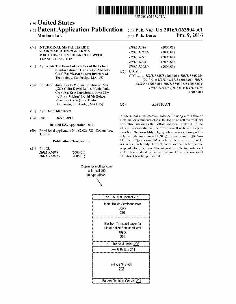
(57) ABSTRACT
A 2-terminal multi-junction Solar cell having a thin film of metal halide semiconductor as the top solar-cell material and crystalline silicon as the bottom solar-cell material. In the illustrative embodiment, the top solar-cell material is a per ovskite of the form AMCIH), where A is a cation, prefer ably methylammonium (CH-NH), formamidinium (RN CH=NRI"), or cesium; Mis metal, preferably Pb, Sn, Ge; H is a halide, preferably Br or Cl; and X-iodine fraction, in the range of 0 to 1, inclusive. The integration of the two solar-cell materials is enabled by the use of a tunneljunction composed of indirect band-gap material.
Metal Halide Semiconductor Stack 210
Electron Transport Layer for Metal Halide Semiconductor
Stack 208
n++ Tunnel Junction 206
p++ SIEmitter 204
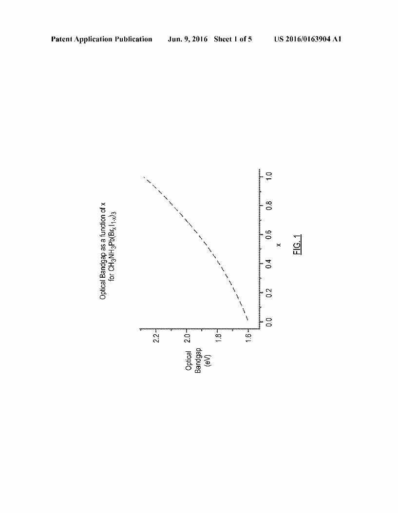
n-Type Si Stack 202
Patent Application Publication Jun. 9, 2016 Sheet 1 of 5 US 2016/O163904 A1
co
co C CD S
S2
US 2016/O163904 A1 Jun. 9, 2016 Sheet 2 of 5 Patent Application Publication
US 2016/O163904 A1 Jun. 9, 2016 Sheet 3 of 5 Patent Application Publication
US 2016/O163904 A1 Jun. 9, 2016 Sheet 4 of 5 Patent Application Publication

US 2016/O163904 A1
35 ZOIL SnOJOdoseW§§5 ŽOLL SnOJOdOSêW
Jun. 9, 2016 Sheet 5 of 5
D-?RIST7||9. –ISE IS ++U
Patent Application Publication
US 2016/0163904 A1
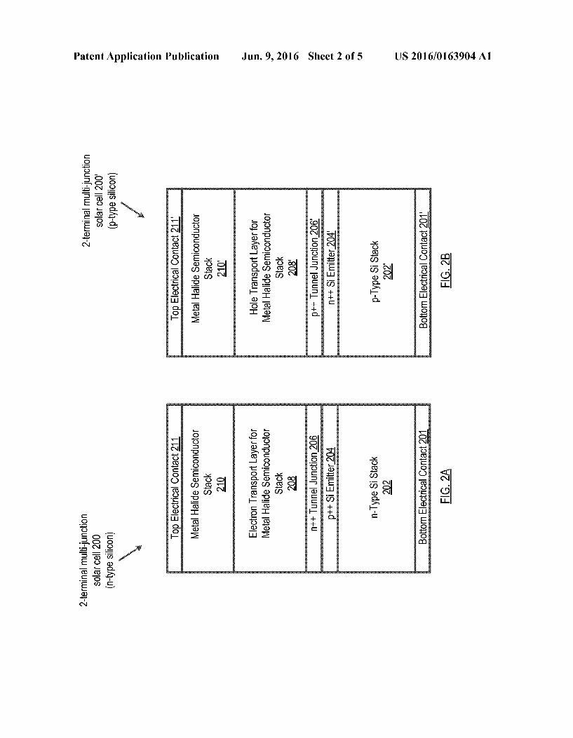
2-TERMINAL METAL HALDE SEMCONDUCTORAC-SILICON
MULTUNCTION SOLAR CELL WITH TUNNEL JUNCTION
STATEMENT REGARDING FEDERALLY SPONSORED RESEARCH
0001. This case claims priority to U.S. patent application 62/086785 filed Dec. 3, 2014 and which is incorporated herein by reference.
STATEMEMT REGARDING FEDERALLY SPONSORED RESEARCH
0002 This invention was made with Government support under Grant Nos. DE-EE0004946 and DE-EE0006707 awarded by the U.S. Department of Enegry. The Government has certain rights in the invention.
FIELD OF THE INVENTION
0003. The present invention relates generally to solar cells.
BACKGROUND OF THE INVENTION
0004 Solar-to-electricity conversion efficiency is the key technical driver influencing photovoltaic (PV) module costs. The record efficiency of crystalline silicon (c-Si) single-junc tion PV devices increased from 25% to 25.6% during the last fifteen years, asymptotically approaching the Shockley Queisser (S-Q) efficiency limit of 29.4%. To exceed this efficiency limit, multi-junction Solar cells have been pro posed. 0005 Multi-junction (MJ) solar cells have multiple p-n junctions made of different semiconductor materials. The p-n junction of each different semiconductor material produces electric current in response to different wavelengths of light. The use of multiple semiconducting materials allows the absorbance of a broader range of wavelengths, improving the cells solar-to-electricity conversion efficiency. 0006 Currently, high-efficiency commercial “tandem’’’ Solar cells (two p-n junctions or "absorbers') are exceedingly expensive, as they are made by growing films of III-V semi conductors epitaxially on single-crystal wafers. Tandem Solar cells have also been made with CIGS, amorphous silicon and organic semiconductors using low-cost processing methods, but these have achieved only modest record cell efficiencies of 23.2, 13.4, and 12.0 percent, respectively. 0007. It was previously noted that PV module efficiency is main driver for reducing PV module prices. Yet, the efficiency of a Solar cell is fundamentally limited by its energy bandgap (E). Silicon, the most widely used material for solar cells, has an E of 1.12 eV, which limits its Shockley-Queisser efficiency to about 29 percent. Because advanced solar-cell technology already approaches the practical theoretical effi ciency limit, the maximum price savings available by further efficiency improvements is finite. To continue extracting cost reduction benefit from efficiency, concepts beyond the S-Q efficiency limit are needed.
SUMMARY OF THE INVENTION
0008. The present invention provides a 2-terminal.MJ Solar cell that avoids some of the disadvantages of the prior art. In some embodiments, the 2-terminal MJ solar cell is a
Jun. 9, 2016
tandem (two p-n junctions) solar cell having a thin film of metal halide semiconductor as the top solar-cell material and c-Si as the bottom solar-cell material. In the illustrative embodiment, the metalhalide semiconductor is a metalhalide perovskite. The integration of the two solar-cell materials is enabled by the use of a tunnel junction composed of indirect band-gap material. 0009. To advance PV module efficiency beyond the S-Q efficiency limit, the inventors considered approaches that sat isfied several criteria:
0010. The increasing importance of capital (fixed) costs on PV module price Suggested to the inventors that any potential efficiency gains must be carefully balanced against increases in equipment requirements and poten tial yield. Thus, a “best approach would be likely to leverage existing manufacturing infrastructure.
0011. The approach should be able to utilize commer cially available production equipment for rapid scaling.
0012. With the foregoing criteria in mind, the inventors recognized that a Si-based Solar cell having an MJ configu ration could leverage the large amount of existing c-Simanu facturing capacity. The inventors realized that a promising approach to Surpassing the efficiency limit would be to reduce the thermalization loss of high energy photons by forming Solar cells in an MJ configuration using materials with differ ent band gaps E. Two-junction Si-based tandems have the highest efficiency entitlement (a maximum of about 39 per cent) when the bandgap of the top sub-cell is between 1.6 and 1.9 eV. However, very few materials exhibit high open-circuit Voltages (V) within this band gap range. As previously mentioned, the E of Si is only 1.12 eV. Thus, although Si could be used for the bottom cell, a different material should be selected for use in the top cell of the multi-junction solar cell.
0013 The inventors recognized that pairing a metal halide semiconductor with c-Si to form an MJ solar cell could be a potentially fruitful approach because of the ability of the former class of materials to be an efficient solar cell material while, at the same time, being deposited at low temperature and requiring low capital expenditure. Metalhalide semicon ductor materials also tend to be earth-abundant, making them suitable for rapid scaling and deployment. Also, unlike III-V materials, metal halide semiconductors would not need to be lattice matched to the Si substrate.
0014. In accordance with the illustrative embodiment, the metalhalide semiconductor used in one of the sub-cells of the inventive solar cell is a perovskite of the form:
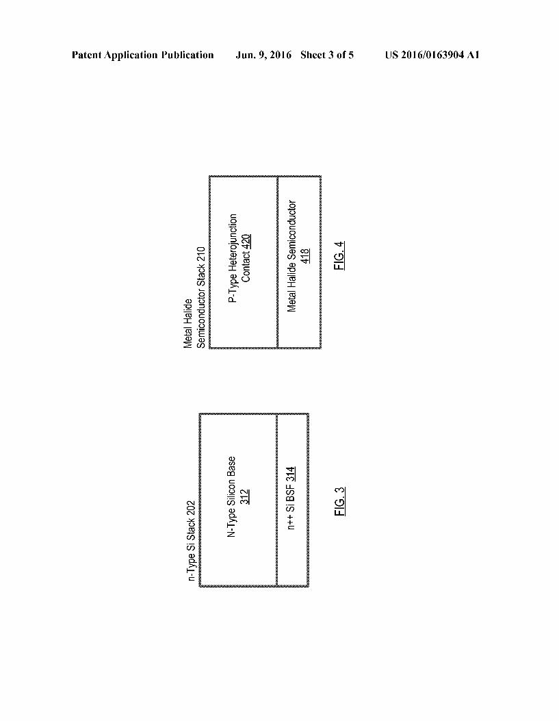
AM(IH). 1.
0.015 where: A is a cation, preferably methylammo nium (CH-NH), formamidinium (RN CH=NRI"), or cesium; 0016 M is a metal; (0017 H is a halide, preferably Br or Cl; and 0018 x iodine fraction, in the range of 0 to 1, inclu sive.
M is preferably Pb, Sn, Ge, Cs, Bi, but most metals may suitably be used including, without limitation, Ca, Sr, Cd, Mn, Fe, Co. Yb, etc. It is notable that alloy mixtures of metal halide semiconductors can be used, as well.
US 2016/0163904 A1
0019 More generally, the metalhalide semiconductor can be represented as:
AMX, 2
0020 where: A is an elemental or molecular cation or combination of cations, including those mentioned above; 0021 M is a metal, including those mentioned above: 0022 X is a halide or combination of halides; and 0023 Z is a number between 1 and 4 describing the relative number of halides with respect to the metal.
0024. When tandems solar cells are made with c-Si as the bottom cell, the ideal bandgap for the top solar cell is about 1.7 to 1.8 eV. Perovskite bandgap can be continuously tuned from 1.6 eV to 2.3 eV by substituting iodide with bromide, as shown in FIG. 1. In some alternative embodiments, metal halide compounds with non-perovskite crystal structure may Suitably be used. For example, simple metal halides such as Bill have abandgap of about 1.7 to 1.8 eV. It is crucial that the large bandgap junction of a tandem Solar cell yield a large open-circuit voltage (V). The V of record devices with CHNHPbl (methylammonium leadiodide perovskite, i.e., A is methylammonium and x=1 in expression 1) is 1.18 V. despite having a bandgap E of only 1.6 eV. 0025. The large open-circuit voltage arises from the unique electrical properties of metal halide perovskites, which makes them highly tolerant of defects. This high defect tolerance has the potential to enable electronic properties for solar cells with high throughput and low-cost solution or physical vapor-deposition processing and without the requirement of expensive single-crystal Substrates. 0026. As such, using a metal halide semiconductor, Such as and without limitation methyl ammonium lead halide per ovskite, in an MJ solar cell with c-Siappeared to the inventors to be a promising candidate. However, no method to electri cally couple the perovskite to the Si sub-cell and simulta neously transmit longer-wavelength light through the perovs kite top-cell to the Si bottom cell in a 2-terminal multi junction configuration is known. 0027 Generally, tunneljunctions are intended for the fore going purpose; that is, to provide low electrical resistance and low optical losses between sub-cells in a multi-cell (multi junction) Solar cell. In the absence of tunnel junction, the p-doped region of the top sub-cell would be directly con nected with the n-doped region of the adjacent Sub-cell. A p-n junction with opposite direction to the other p-n junctions would appear between the two adjacent cells. This would result in photo-voltage that is lower than if there were no parasitic diode. The tunnel junction is used to decrease this effect. As typically implemented, a tunnel junction is simply a wide band gap, highly doped diode. In order to avoid a reduction in the performance (efficiency) of multi-junction Solar cells, the tunnel junction must be transparent to wave lengths absorbed by the next cell in the multi-junction solar cell. 0028 Inter-band tunneling (i.e., a tunnel junction) is used in III-V tandem solar cells. The tunnel junction of these solar cells is typically formed from direct-bandgap semiconductors in which parasitic absorption of light is a design constraint. Such a tunnel junction would therefore be unsuitable for use in conjunction with embodiments of the invention. Alterna tively, direct-bandgap metal-like semiconductors are used as tunnel junction alternatives (e.g., transparent conducting oxides such as fluorine-doped tin oxide or tin-doped indium
Jun. 9, 2016
oxide, etc.). These materials, although very transparent in the visible spectrum, have reduced transparency at longer wave lengths due to free carrier absorption. As a consequence. Such tunnel junction alternatives are not suitable for use in con junction with embodiments of the present invention. 0029. In accordance with embodiments of the invention, multi-junction Solar cells incorporate a tunneljunction that is formed from an indirect bandgap semi-conductor. The indi rect bandgap results in a relatively reduced (compared to a direct-bandgap material) tendency to absorb light. In accor dance with the illustrative, embodiment, the indirect bandgap semiconductor is silicon and the resulting tunnel junction is quite transparent to relatively longer wavelength (i.e., longer than the wavelength-range of visible portion of the EM spec trum) light. 0030. In accordance with the illustrative embodiment, a 2-terminal metal halide perovskite/c-Si MJ solar cell is formed via monolithic integration, wherein a thin film of the Sub-cell including the aforementioned perovskite is grown on top of a wafer-based crystalline silicon sub-cell. A tunnel junction facilitates electron tunneling from the electron selec tive contact of the top perovskite cell into the p-type emitter of the bottom silicon cell, instead of a recombination layer being used in other perovskite tandem systems. As previously men tioned, in accordance with the illustrative embodiment, the tunnel junction is made out of an indirect band gap material, Such as silicon, thereby enabling electrical coupling with minimal parasitic absorption within the tunnel junction. 0031 Furthermore, due to the conduction band alignment between the tunnel junction and the perovskite cell's electron selective contact (TiO), no transparent conducting oxide (TCO) such as fluorine-doped tin oxide (FTO) or tin-doped indium oxide (ITO) is required, further reducing parasitic optical absorption in the perovskite/silicon multi-junction cell. In fact, this approach to the tunneljunction resulted in an open circuit voltage of about 1.6 V, which is a high value for a CH-NHPbl perovskite/Simulti-junction solar cell. 0032. In some embodiments, the invention provides an article comprising a two-terminal MJ solar cell, wherein the Solar cell comprises a bottom Sub-cell comprising a silicon base; a tunnel junction disposed above the silicon base, wherein the tunnel junction comprises a material character ized by an indirect band gap; and a top Sub-cell disposed above the tunneljunction, wherein the top Sub-cell comprises a metal halide perovskite. 0033. In some embodiments, the invention provides an article comprising a two-terminal multi-junction Solar cell, wherein the solar comprises a c-Si sub-cell; a bottom elec trode disposed proximal to a bottom surface of the c-Si sub cell; a tunnel junction disposed on the c-Si Sub-cell, wherein the tunnel junction comprises a material having an indirect band gap; a metal halide semiconductor Sub-cell disposed on the tunneljunction; and a top electrode disposed on proximal to a top surface of the metal halide semiconductor sub-cell. 0034. In some embodiments, the c-Si sub-cell comprises a silicon base, a back Surface field disposed proximal to a bottom Surface of the silicon base, and an emitter disposed proximal to a top Surface of the silicon base. In some embodi ments, the metal halide semiconductor Sub-cell comprises a transport layer, wherein the transport layer is an electron transport layer when a silicon base in the crystalline silicon Sub-cell is n-type silicon and wherein the transport layer is a hole transport layer when the silicon base in the crystalline silicon Sub-cell is p-type silicon; a layer of metal halide semi

US 2016/0163904 A1
conductor; and a heterojunction contact, wherein the hetero junction contact is p-type when the silicon base is n-type silicon and the heterojunction contact is n-type when the silicon base is p-type silicon. 0035. In some embodiments, the invention provides a method for forming a two-terminal MJ solar cell, wherein the method comprises forming a c-Si Sub-cell; forming a tunnel junction on the c-Si Sub-cell from indirect bandgap material; and forming a metal halide semiconductor Sub-cell. 0036. In some embodiments, the metal halide semicon ductor is a metalhalide perovskite. In some embodiments, the metal halide perovskite is methylammonium lead iodide per ovskite.
BRIEF DESCRIPTION OF THE DRAWINGS
0037 FIG. 1 depicts plot 100 showing the bandgap of mixed halide perovskite as a function of bromine fraction, X. 0038 FIG. 2A depicts 2-terminal metal halide semicon ductor/c-Simulti-junction Solar cell based on n-type silicon, in accordance with an illustrative embodiment of the present invention. 0039 FIG. 2B depicts 2-terminal metal halide semicon ductor/c-Simulti-junction Solar cell based on p-type silicon, in accordance with an illustrative embodiment of the present invention. 0040 FIG. 3 depicts further detail of a silicon sub-cell stack in the solar cell of FIG. 2A. 0041 FIG. 4 depicts further detail of a metal halide semi conductor sub-cell stack in the solar cell of FIG. 2A. 0042 FIG.5 depicts a method for forming the solar cell of FIG. 2A 0043 FIGS. 6A through 6E depict the sequential forma tion of a solar cell in accordance with the method of FIG. 5.
DETAILED DESCRIPTION
0044) Definitions. A definition for each of the terms listed below is provided for use in understanding the description and interpreting the appended claims.
0045. About when referencing a measurement (e.g., diameter, length, thickness, etc.) means within 15% of the stated value.
0046 “Crystalline silicon' means monocrystalline, multi-crystalline, or polycrystalline.
0047. “Tandem solarcell means a solarcell having two different absorbers (e.g., silicon and a metalhalide semi conductor).
0048 “Multi-junction’solar cell means a solarcell hav ing two or more absorbers (p-n junctions) in the same solar cell.
0049 “Nanowire” means electrically conductive mate rial that is less than 1000 nanometers in diameter and greater than 1000 nanometers in length.
0050 “2-terminal solar cell refers to a tandem solar cell in which the two sub-cells (e.g., the perovskite sub cell and the silicon sub-cell) are electrically connected in series with each other. This is distinguished, for example, from a 4-terminal tandem cell wherein the two Sub-cells are not electrically connected to each other and instead are operated independently.
0051 Solar Cell. 0052 FIG. 2A depicts a schematic representation of 2-ter minal, metal halide semiconductor/c-Simulti-junction Solar cell 200 with an n-type silicon base. The solar cell includes:
Jun. 9, 2016
bottom electrical contact 201, n-type Sistack 202, p" Si emitter 204, n' Si tunnel junction 206, electron-transport layer 208 for the metal halide semiconductor stack, metal halide semiconductor stack 210, and top electrical contact 211. 0053 FIG. 2B depicts a schematic representation of 2-ter minal, metal halide semiconductor/c-Simulti-junction Solar cell 200' with an p-type silicon base. The solar cell includes: bottom electrical contact 201'. p-type Sistack 202', n' Si emitter 204", p" Si tunnel junction 206", hole-transport layer 208 for the metal halide semiconductor stack, metal halide semiconductor stack 210", and top electrical contact 211". 0054 Solar cells 200 and 200' are top illuminated; that is, their architecture is such that they are intended to be illumi nated from the “top” as oriented in FIGS. 2A and 2B. That is, light is received at the top electrical contact 211 or 211". It will be appreciated, however, that depending upon packaging or other constraints, the top electrical contact might not be ori ented “above' other layers when in use. As used in this description and the appended claims, the descriptors "above.” “top,” “below,” “bottom,” etc. are referenced relative to the light receiving Surface, which is top electrical contact 211. In other words, regardless of the orientation of solar cell 200, the top electrical contact is always considered to be “above' the other elements of the solar cell shown in FIG. 2A. Therefore, when a first layer is described as being “above' or "on top of a second layer, it means the first layer is relatively closer to the top electrical contact than the second layer is to the top elec trical contact. Conversely, when a first layer is described as being “below.” etc., a second layer, it means the first layer is relatively further from the top electrical contact than is the second layer. 0055. Furthermore, the terms “above,” “on top of.” “below, etc., when describing two layers, do not necessarily mean that the layers are “directly adjacent to or “in contact with one another. 0056. It will be appreciated that the structure of the two Solar cells are similar to one another, but any material that is p-type in solar cell 200 of FIG. 2A will be n-type in solar cell 200' of FIG.2B. Similarly, any material that is n-type in solar cell 200 will be p-type in solar cell 200'. And, of course, electron transport layer 208 of solar cell 200 is replaced by hole transport layer 208 in solar cell 200'. For brevity, this disclosure will only discuss solar cell 200 based on n-type silicon; those skilled in the art will understand how to make and use solar cell 200' based on p-type silicon in light of the disclosure concerning solar cell 200. 0057 FIG. 3 depicts further detail of an embodiment of n-type silicon Stack 202, including n-type silicon 312 and n-type silicon back surface field (BSF) 314. The silicon por tion (“the silicon sub-cell”) of solarcell 200 (or 200') includes the Sistack 202 (or 202') and p" Siemitter 204. 0058 FIG. 4 depicts further detail of an embodiment of metal halide semiconductor stack 210, including metal halide semiconductor 418 and organic p-type heterojunction contact 420. The metal halide semiconductor portion (“the metal halide semiconductor sub-cell') of solar cell 200 (or 200') includes metal halide semiconductor stack 210 (or 210") and electron-transport layer 208 (or hole transport layer 208). 0059 Bottom electrical contact 201 and top electrical con tact 211 are the electrical contacts by which electrical current is withdrawn from the solar cell. Both such contacts com prise, of course, electrically conductive material. In the illus trative embodiment, the solar cell is illuminated from the top.

US 2016/0163904 A1
As such, electrical contact 211 must be physically adapted (either by virtue of its material composition or configuration) to enable Sunlight to pass and enter the underlying layers of Solar cell 200.
0060 Solar cell 200 also includes a conventional anti reflection coating (not depicted) over the top electrical con tact to reduce surface reflection.
0061 Method of Fabrication. 0062 FIG. 5 depicts method 500 in accordance with an illustrative embodiment of the present invention. Method 500 includes: 0063 operation 501 (forming silicon sub-cell); 0064 operation 502 (forming tunnel junction); 0065 operation 503 (forming bottom electrical contact); 0066 operation 504 (forming electron transport layer); 0067 operation 505 (forming metalhalide semiconductor stack); and 0068 operation 506 (forming top electrical contact). These operations are discussed in detail below in conjunction with FIGS. 6A through 6E. 0069. With continuing reference to FIG.5 and with refer ence to FIGS. 2, 3, and FIG. 6A, in operation 501, the silicon Sub-cell is formed. In some embodiments, this operation includes the steps of texturing the back Surface of n-type silicon wafer 630 (also referred to as the “base'), implanting boron on the top surface of the Sibase and implanting phos phorous on the textured back surface of the Sibase. This is performed at sufficiently high doping levels such that, after annealing, p" silicon emitter 204 is formed at the top surface of Siwafer or base 630 and n-type silicon BSF 314 is formed at the textured back surface. The base has a thickness that is typically in the range of about 10 to about 1000 microns, emitter 204 has a thickness that is typically in the range of about 1 to about 1000 nanometers, and BSF 314 (which is optional), has a thickness that is typically in the range of about 1 to 1000 nanometers.
0070. It is notable that the doping of base silicon 630 is not of primary importance. Rather, what is of particular impor tance is that there is a p"Si/n"Si tunnel junction on top and n" Sion the bottom of Sibase 630 for Solar cell 200 of FIG. 2A or ann"Si/p"Si tunnel junction on top and p" Sion the bottom of the Sibase for Solar cell 200' of FIG. 2B. As those skilled in the art will understand, if the Si base doping is changed from what was discussed in the illustrative embodi ment, the emitter is on the bottom of the Sibase instead of on top of it. This is known as a “rear-emitter.” (0071 Referring now to FIG. 5 and FIGS. 2, 4, and 6B in operation502, Si-based tunnel junction 106 is formed on top of p" silicon emitter 204. The tunnel junction facilitates carrier recombination (i.e., holes from the n-type silicon base passing through the p-type emitter and electrons from organic-inorganic semiconductor 418 passing through elec tron transport layer 108). Tunnel junction 106 is formed by creating a highly-doped silicon layer (doping concentration greater than 10" atoms of dopant/cm) directly on p" silicon emitter 204. In this embodiment, using an n-type silicon wafer, the tunnel junction is n' doped. If the silicon wafer were p-type, the tunnel junction would, of course, be p" doped. 0072. In the illustrative embodiment, tunnel junction 106
is formed by depositing degenerately doped n" amorphous silicon using plasma-enhanced chemical vapor deposition (PECVD).
Jun. 9, 2016
0073. In addition to facilitating carrier recombination, in accordance with the present teachings, tunneljunction 206 is physically adapted to transmit wavelengths of EM radiation longer than those in the visible range. Although silicon is used to form the tunnel junction in the illustrative embodiment, other materials having an indirect band-gap may suitably be used for forming a tunnel junction in other embodiments. (0074) Referring now to FIGS. 5, 3 and 6C, in operation 503, the bottom electrode is formed. In the illustrative embodiment, the bottom electrode is formed via a standard back metallization process. In some embodiments, this met allization comprises multiple layers, each layer formed from a different metal, and each layer being in the range from tens to hundreds of nanometers in thickness. Although all the metals are necessarily electrically conductive, the presence of more than one metal in the bottom electrode is occasioned by the fact that properties such as adhesion and the ability to act as a metal diffusion barrier are important, but not necessarily possessed to the required degree by the metal with the highest electrical conductivity. For example, in Some embodiments, the metals chosen include: a layer of titanium having a thick ness of about 20 nanometers and used for adhesion, a layer of palladium having a thickness of about 20 nanometers and used as a metal diffusion barrier, and a layer of silver having a thickness of about 300 nanometers and used for electrical conduction. Back metallization layer 632 serves as a negative electrical contact for the solar cell 200.
0075. The silicon wafer (with the various deposited lay ers) is optionally diced into Smaller pieces (typically of uni form size and in a range from about 1x1 cm to about 2x2 cm) following back metallization. In some other embodi ments, dicing could be done at a later stage of the process (or not at all). (0076 Referring now to FIGS. 5, 2, and 6D in operation 504, electron transport layer 208 is formed. This serves as the n-type heterojunction contact for the organic-inorganic semi conductor sub-cell. It is notable that in an embodiment in which the starting Si wafer was p-type, this operation would be to form a hole transport layer. 0077. In the illustrative embodiment, electron transport layer 208 comprises a layer of titanium dioxide (TiO). In Some embodiments, this layer of titanium dioxide is depos ited, to a thickness of tens of nanometers, using atomic layer deposition (ALD). In the illustrative embodiment, the ALD deposited layer has a thickness of about 30 nanometers, but the thickness of this layer can be a minimum of about 1 nanometer to a maximum of about 500 nanometers.
0078. In some embodiments, an optional mesoporous layer of titanium dioxide is deposited on the ALD-deposited layer, such as by spin coating a solution of TiO2 nanoparticles and subsequently sintering, such as at about 500° C. In the illustrative embodiment, the mesoporous layer has a thick ness of about 300 nanometers. To the extent that the mesopo rous layer is present, the thickness of this layer can be a minimum of about 1 nanometer to a maximum of about 2000 nanometerS.
0079. In some other embodiments, a material other than titanium dioxide, such as, without limitation, C60, Phenyl C61-butyric acid methyl ester (PCBM), SnO, or ZnO, is used to form electron transport layer 208. 0080 Referring now to FIGS. 5, 2, 4, and 6E, in operation 505, metal halide semiconductor stack 210 is formed. As
US 2016/0163904 A1
depicted in FIG. 4, stack 210 comprises metal halide semi conductor material 418 and p-type heterojunction contact (hole transport layer) 420. 0081. In the illustrative embodiment, metal halide semi conductor material 418 is methyl ammonium lead halide perovskite and p-type heterojunction contact 420 is 2,2,7,7- Tetrakis-(N,N-di-4-methoxyphenylamino)-9.9'-spirobifluo rene (“spiro-OMeTAD). 0082 In some embodiments, the perovskite is deposited via a two-step conversion method modified from a procedure developed by Burschka et al. (J. Burschka et al., Nature v499, p316 (2013). Specifically, Pbl is dissolved in N,N-dimethyl formamide (DMF) and is deposited by spin coating and dried for 30 minutes at 70° C. and then cooled to room temperature. Conversion occurs by Submersion in an isopropyl alcohol (IPA) bath containing methylammonium iodide (MAI), resulting in a perovskite layer with a chemical formula CHNHPbl. In the illustrative embodiment, the perovskite layer fills the pores of the titanium dioxide of electron trans port layer 208 and forms a capping layer thereon having a thickness of about 150 nanometers. More generally, the thick ness of the metal halide semiconductor will be in the range of about 150 to about 2000 nanometers. Thus, metal halide semiconductor 418 is formed. As knownto those skilled in the art, there are a variety of ways to form and deposit perovskite. In conjunction with the present disclosure, those skilled in the art will be able to suitably select other deposition methods, as desired. I0083. The spiro-OMeTAD, as organic p-type heterojunc tion contact 420, was deposited on the perovskite by spin coating. Contact 420 will typically have a thickness in the range of about 1 to about 500 nanometers. In the illustrative embodiment, the resulting layer of spiro-OMeTAD was doped with spiro-(TSFI) in a process developed by Nguyen and some of the present inventors (Nguyen et al., J. Am. Chem. Soc. v. 136, p10996 (2014)) and additionally included the organic additive tert-butylpyridine (tPP). In some other embodiments, other materials known to those skilled in the art can be used to form the hole-transport layer (i.e. p-type heterojunction contact 420) in known fashion. 0084. Referring now to FIGS. 5, 2, 4, and 6E, in operation 506, top electrical contact or electrode 211 is formed, in the illustrative embodiment, as mesh of silver nanowires 644. The mesh is deposited in a multi-step process wherein the nanowires are sprayed from solution onto a plastic (PET) film. The silver nanowires are then transferred from the PET to the spiro-OMeTAD layer via mechanical transfer through, for example, the application of pressure (e.g., 2500 psi). The pressure is applied across a diaphragm through the applica tion of compressed N to ensure uniform pressure. Other techniques for applying pressure to accomplish the mechani cal transfer, as will occur to those skilled in the art in light of the present disclosure, may suitably be used. In some embodi ments, an electrically conductive material (e.g., a metal, etc.) is deposited as a contact pad around the perimeter of the mesh of silver nanowires to increase the efficiency of current col lection as well as to provide a means of electrical contact to the mesh of silver nanowires. In the illustrative embodiment, the contact pad comprises silver and is deposited via thermal evaporation to a thickness of about 300 nanometers. In some alternative embodiments, other materials suitable for forming transparent electrodes (i.e., transparent to light over the desired range of wavelengths) are Suitably used as top elec trical contact 211. A partial and non-limiting list of Such
Jun. 9, 2016
suitable materials include: ITO, FTO, AZO, other transparent electrically conductive oxides, and graphene. I0085 Although the description has focused on a double junction Solar cell, the present teachings can be applied to create a Solar cell having more than two junctions. For example, consider the following triple-junction architecture for a perovskite/silicon solar cell in accordance with the present teachings. The third junction is disposed on top of the “original perovskite layer in the double-junction architec ture and the original perovskite and silicon Sub-cells remain Substantially the same as disclosed. The third junction can be formed from another perovskite having a different composi tion than the original perovskite. The tunnel junction in the silicon itself would not change and the first heterojunction layer (electron or hole transport layer) is suitably generic.
Example: Formation of 2-terminal perovskite/c-Si multi-junction Solar cell.
I0086 Formation of silicon sub-cell. A double-side pol ished <100> n-type float Zone silicon (Si) wafer (1-5C2-cm, 300 um thickness) was procured. The front side of the wafer was coated with a silicon nitride (SiN) film having a thick ness of about 300 nm. The purpose of the film is to protect the planarity of the silicon front Surface during Subsequent ran dom pyramidal texturing step on the back side of the silicon starting wafer. Texturing was accomplished using 3% weight KOH solution in de-ionized (DI) water mixed with isopro panol (6:1 volume), 80° C. etch for 20 minutes. I0087. The SiN protective layer was removed using hydrofluoric acid (HF). The sample was then cleaned using the RCA cleaning procedure for silicon wafers (RCA1 = 10 minute, 80° C. dip in 5:1:1 NHOH:HO:HO, RCA2=10 minute, 80° C. dip in 5:1:1 HC1:HO:HO) as follows:
deionized (DI) water dip->HF dip->RCA1clean->DI water dip->HF dip->DI water dip->RCA2clean->DI water dip->HF dip->DI water dip->N, dying.
I0088 Boron was then implanted into the planar front sur face (''B with 1.8x10'cmi dose, 6 keV implantation energy) and phosphorus in the textured back surface ('P with 4x10" cm dose, 10 keV implantation energy) of the wafer. The wafer was then cleaned again using RCA cleaning pro cedure, dipped in dilute HF solution for oxide removal, cleaned with DI water, and dried with N. The p-type B emitter and n-type P back surface field (BSF) were formed simultaneously by drive-in annealing at 960° C. in an N ambient for 30 minutes.
0089. After the emitter and BSF formation, the wafers were cleaned again with RCA cleaning procedure, and then dipped in dilute HF solution for oxide removal, cleaned with DI water, and dried with N. (0090. The n"/p" tunnel junction was then formed by depositing heavily doped n" hydrogenated amorphous sili con (a-Si:H) using plasma-enhanced chemical vapor deposi tion (PECVD). First, an intrinsica-Silayer having a thickness of about 2-3 mm-thick was deposited on top of the p" emitter using PECVD (temperature of 250° C., pressure of 150 mTorr, 55 sccm of SiH gas with a plasma power density of 0.16 W/cm). Next, an a-Si:H layer having a thickness of about 30 nm was deposited at 250° C. at a pressure of 200 mTorr (55 sccm of SiHa gas and 50 sccm of 1% PH in Higas) and plasma power density of 0.13 W/cm. The nearly finished

US 2016/0163904 A1
Sisub-cell was then annealed in Nambient at 680° C. for 15 minutes to activate the dopants and partially crystallize the amorphous layer. 0091 After forming the tunnel junction, square-shaped mesas were formed using photolithography. The mesas were 1.1x1.1 cm and spaced apart 1.4x1.4 cm. The mesas were formed as follows. Positive photoresist was deposited on both sides of the silicon wafer (Shipley 1813 photoresist spun at 4000 rpm for 40 seconds, baked at 115° C. for 1 minute). The front side underwent mesa patterning, was exposed for 4.5 seconds, and developed in CD-26 developer for approxi mately 1 minute. The back side was left unexposed to protect the BSF on the back side during the subsequent mesa forma tion step. Mesas were then formed on the front side of the Si wafer using reactive ion etching (RIE) to etch 300 nm of the silicon layer, removing the n" tunneljunction and most of the p" emitter outside the square-shaped mesa. The remaining photoresist mask was then removed using solvent clean (3 minute Sonication in acetone, 3 minute Sonication in IPA, rinsing with DI water and drying with N). 0092 Next, the nascent Si sub-cell was dipped in dilute HF for oxide removal, cleaned with DI water, and dried in N. The back metallization was then formed via electron-beam evaporation. A stack of Ti/Pd/Ag/Pt with layer thicknesses of about 20/20/300/30 nm was chosen (Ti for adhesion, Pd for metal diffusion barrier, Ag for electrical conduction, and Pt for corrosion protection during perovskite sub-cell process ing) followed by rapid thermal anneal (400° C. in N for 5 minutes) to improve metal adhesion. 0093. This was followed by dipping in dilute HF for oxide removal, cleaning in DI water, and drying in N. Next a layer of TiO, was deposited via atomic layer deposition to a thick ness of 30 nm (Cambridge NanoTech Savannah ALD tool, 150° C. substrate temperature, 80° C. precursor temperature, 440 mTorr base pressure, and 20 sccm N. carrier gas). To achieve the desired TiO layer thickness, 604 cycles of puls ing HO vapor for 0.02 seconds were performed followed by a seven-second wait period, followed by pulsing TDMAT vapor for 0.2 seconds, and then a seven-second wait. 0094. After depositing the TiO, via ALD deposition, pho toresist was deposited on the TiO, to protect it during the following step (Shipley 1818 photoresist spun at 4000 rpm for 40 seconds, baked at 115° C. for 1 minute). Dilute HF with 10% concentration in DI was then used to dissolve the TiO, layer that was deposited on the back metallization during the ALD process. 0095. The Si sub-cells with overlying electron transport layer (TiO) were then laser-scribed from the back to form 1.4x1.4 cmunits. After mechanical cleaving, individual 1.4x 1.4 cm sub-cells, each with a 1.1x1.1 cm square-shaped mesa (active junction area) in the middle and a TiO layer on the planar front surface protected by photoresist resulted. 0096. Formation of Perovskite sub-cell. The sub-cells were prepared for further processing by Sonication in acetone for 5 minutes, sonication in IPA for 5 minutes, rinsing with DI water, and drying with N, 5 minutes of UV-OZone cleaning, and sintering for 30 minutes at 450° C. After cool down, mesoporous TiO films were spun onto the ALD deposited layer of TiO, at 4000 rpm for 30 seconds and sintered at 450° C. The spin-coating solution was a 1:3 dilution of 18-NRT TiO, paste (Dyesol) in ethanol. 0097 All previous steps were performed in ambient atmo sphere. The remainder of device fabrication was performed in a Na glovebox with <5 ppm O and H2O. The sub-cells were
Jun. 9, 2016
dried by heating to 500° C. with a hot-air gun for 30 minutes and immediately brought into the glovebox. A 1.3 molar solution of Pbl was prepared by dissolving Pbl (Aldrich, 211168) into anhydrous DMF (Acros, 32687) and stirring on a hotplate at 100° C. The DMF was filtered through a 200 nm PTFE filter(Pall, 4552) prior to adding to the solution in order to remove particulates. Methylammonium iodide (MAI) was purchased from Dyesol and used as received. A solution of 10 milligram (mg) MAI per 1 milliliter (mL) anhydrous IPA (Acros. 61043) was prepared and allowed to dissolve at room temperature. A pure IPA rinse Solution was prepared as well. The IPA was filtered through a 20 nm PTFE filter prior to adding to the Solutions in order to remove particulates. 0098. After the sub-cells were cooled to room tempera ture, 100 microliters (uL) of the 100° C. Pbl/DMF solution was pipetted onto the substrate and spun at 6500 rpm for 90 seconds. The resulting film was dried for 30 minutes on a 70° C. hotplate. After cooling, the films were dipped in the MAI/ IPA solution for 15 minutes. Films were then rinsed in IPA, dried by spinning at 4000 rpm for 30 seconds, and placed back on the 70° C. hotplate for 30 minutes. (0099. After cooling, 75uL of a spiro-OMeTAD (Lumtec, LT-S922) solution was spun on top perovskite layer at 4000 rpm for 30 seconds. The spiro-OMeTAD was a 163 millimo lar (mM) solution of spiro-OMeTAD in anhydrous chlo robenzene (Sigma-Aldrich, 284.513). The spiro-OMeTAD was dissolved by placing on a hotplate at 70° C. for more than 30 minutes. 534 mM oftert-butyl pyridine (Aldrich, 142379) and 86 mM of Li-TFSI (Aldrich, 15224) dissolved as 520 mg/mL in anhydrous acetonitrile (Acros, 61096) were added to the spiro-OMeTAD solution. 8 mol % of the spiro OMeTAD was spiro-OMeTAD(TFSI)2, resulting in 16% of spiro-OMeTAD molecules being chemically oxidized to ensure electrical conductivity in the spiro-OMeTAD layer. The spiro-OMeTAD(TFSI)2 was synthesized as reported elsewhere in literature. After the spiro-OMeTAD solution was prepared, it was filtered through a 20 nm Al-O filter (Whatman, 6809-3102) to remove any aggregates and par ticulates. Films were then removed from the glovebox and stored overnight in a desiccator at 20% relative humidity (RH). 0100. A mesh of silver nanowires on PET was transferred on top of the spiro-OMeTAD layer. A spring-loaded ball bearing, rather than gas pressure, was used to better control the pressure applied to the silver nanowire mesh. The spring was set to 500 grams force at full depression of the ball into the housing. After transfer of the silver nanowire mesh, a pad of silver was thermally evaporated to a thickness of about 300 nm through a patterned shadow mask around the edges of the device leaving 1x1 cm active area in the middle of the 1.1x 1.1 cm mesa. The silverhelped reduce the unnecessary series resistance in the silver nanowires by not limiting the current collection to one geometrical direction. The nearly completed device was light-soaked under visible illumination for 10 minutes then stored in a desiccator for 12 hours before apply ing an anti-reflective coating. The anti-reflective coating was an LiF film having a thickness of about 111 nm. This thick ness was optimized to provide anti-reflection for the visible spectrum.
0101. It is to be understood that the disclosure teaches just one example of the illustrative embodiment and that many variations of the invention can easily be devised by those

US 2016/0163904 A1
skilled in the art after reading this disclosure and that the scope of the present invention is to be determined by the following claims. 0102. With respect to variations, those skilled in the art will recognize that BSF (i.e., BSF 314) is one of several possible back contacts. For example, in Some architectures, rather than BSF, a heterojunction layer is used for back con tact, either amorphous silicon or poly Silicon. Also, in some architectures, a thin passivation layer is disposed between base-emitter and base-back contact. For example, in a hetero junction-intrinsic-thin (HIT) cell, wherein 2 to 3 nanometers of intrinsic amorphous silicon is included between base-emit ter and base-back contact, wherein both the emitter and back contact are amorphous silicon, which forms a heterojunction with the crystalline silicon base. Other embodiments include a tunnel-oxide-passivated contact (TOPCon), wherein about 1.5 nanometers of SiO, is included between base-emitter and base-back contact, wherein both the emitter and back contact are polycrystalline silicon. What is claimed is: 1. An article comprising a two-terminal multi-junction
Solar cell comprising: a crystalline silicon Sub-cell; a bottom electrode disposed below a bottom surface of the
crystal silicon Sub-cell; a tunnel junction disposed above the crystal silicon Sub
cell, wherein the tunnel junction comprises a material having an indirect band gap:
a metal halide semiconductor sub-cell disposed above the tunnel junction; and
a top electrode disposed above a top surface of the metal halide semiconductor sub-cell.
2. The article of claim 1 wherein the metal halide semicon ductor is defined by the formula AM(IH), where A is a cation, M is a metal, H is a halide, and X, which is iodine fraction, falls in a range of 0 to 1, inclusive.
3. The article of claim 1 wherein the metal halide semicon ductor is a metal halide perovskite.
4. The article of claim 1 wherein the crystalline silicon Sub-cell comprises a silicon base, a back Surface field dis posed proximal to a bottom surface of the silicon base, and an emitter disposed proximal to a top surface of the silicon base.
5. The article of claim 1 wherein the metal halide semicon ductor Sub-cell comprises:
a transport layer, wherein the transport layer is an electron transport layer when a silicon base in the crystalline silicon Sub-cell is n-type silicon and wherein the trans port layer is a hole transport layer when the silicon base in the crystalline silicon Sub-cell is p-type silicon;
a layer of metal halide semiconductor; and a heterojunction contact, wherein the heterojunction con
tact is p-type when the silicon base is n-type silicon and the heterojunction contact is n-type when the silicon base is p-type silicon.
6. The article of claim 5 wherein the transport layer com prises TiO,
7. The article of claim 5 wherein the metal halide semicon ductor is a metal halide perovskite.
8. The article of claim 5 wherein the heterojunction contact comprises spiro-OMeTAD.
Jun. 9, 2016
9. The article of claim 1 wherein the tunnel junction com prises silicon.
10. The article of claim 1 wherein the material having the indirect band gap is silicon.
11. The article of claim 1 wherein the top electrode com prises a mesh of silver nanowires.
12. An article comprising a two-terminal multi-junction Solar cell comprising:
a bottom Sub-cell comprising a silicon base; a tunnel junction disposed above the silicon base, wherein
the tunnel junction comprises a material characterized by an indirect band gap; and
a top Sub-cell disposed above the tunnel junction, wherein the top Sub-cell comprises a metal halide perovskite.
13. The article of claim 12 further comprising a mesh of silver nanowires disposed above the top Sub-cell and serving as a top electrical contact of the Solar cell.
14. The article of claim 12 wherein: the bottom sub-cell further comprises a n++ back surface
field and a p--+ emitter, and the top sub-cell further comprises a hole transport layer and
an organic p-type heterojunction contact. 15. A method for forming a two-terminal multi-junction
Solar cell comprising: forming a crystalline silicon Sub-cell; forming, from a material characterized by an indirect band
gap, a tunnel junction above the crystalline silicon Sub cell; and
forming a metal halide semiconductor sub-cell above the tunnel junction.
16. The method of claim 15 and further comprising form ing a top electrical contact by depositing a mesh of silver nanowires above the metal halide semiconductor sub-cell.
17. The method of claim 15 wherein forming the metal halide semiconductor sub-cell further comprises:
forming a transport layer above the tunnel junction, wherein the transport layer is an electron transport layer when a silicon base in the crystalline silicon sub-cell is n-type silicon and wherein the transport layer is a hole transport layer when the silicon base in the crystal sili con Sub-cell is p-type silicon;
depositing metal halide semiconductor above the transport layer; and
depositing a heterojunction contact above the metal halide semiconductor, wherein the heterojunction contact is p-type when the silicon base is n-type silicon and the heterojunction contact is n-type when the silicon base is p-type silicon.
18. The method of claim 15 wherein the metal halide semi conductor is defined by the formula APb(IH), where A is a cation, H is a halide, and X, which is iodine fraction, falls in a range of 0 to 1, inclusive.
19. The method of claim 18 wherein forming the tunnel junction further comprises:
depositing degenerately doped amorphous silicon on the crystalline silicon Sub-cell; and
activating the dopants by annealing the amorphous silicon. 20. The method of claim 15 wherein the metal halide semi
conductor is methylammonium lead iodide perovskite. k k k k k